

ICSI IC61S6432-100PQ, IC61S6432-100PQI, IC61S6432-100TQ, IC61S6432-100TQI, IC61S6432-117PQ Datasheet
...
IC61S6432
Integrated Circuit Solution Inc. 1
SSR016-0A 09/13/2001
Document Title
64K x 32 Pipelined Sync. SRAM
Revision History
Revision No History Draft Date Remark
0A Initial Draft September 13,2001
The attached datasheets are provided by ICSI. Integrated Circuit Solution Inc reserve the right to change the specifications and
products. ICSI will answer to your questions about device. If you have any questions, please contact the ICSI offices.
IC61S6432
2 Integrated Circuit Solution Inc.
SSR016-0A 09/13/2001
ICSI reserves the right to make changes to its products at any time without notice in order to improve design and supply the best possible product. We assume no responsibility for any errors
which may appear in this publication. © Copyright 2000, Integrated Circuit Solution Inc.
FEATURES
• Internal self-timed write cycle
• Individual Byte Write Control and Global Write
• Clock controlled, registered address, data and
control
• Pentium™ or linear burst sequence control using
MODE input
• Three chip enables for simple depth expansion
and address pipelining
• Common data inputs and data outputs
• Power-down control by ZZ input
• JEDEC 100-Pin LQFP and PQFP package
• Single +3.3V power supply
• Two Clock enables and one Clock disable to
eliminate multiple bank bus contention
• Control pins mode upon power-up:
– MODE in interleave burst mode
– ZZ in normal operation mode
These control pins can be connected to GNDQ
or VCCQ to alter their power-up state
• Industrial temperature available
DESCRIPTION
The ICSI IC61S6432 is a high-speed, low-power synchronous
static RAM designed to provide a burstable, high-performance,
secondary cache for the Pentium™, 680X0™, and PowerPC™
microprocessors. It is organized as 65,536 words by 32 bits,
fabricated with ICSI's advanced CMOS technology. The
device integrates a 2-bit burst counter, high-speed SRAM
core, and high-drive capability outputs into a single monolithic
circuit. All synchronous inputs pass through registers
controlled by a positive-edge-triggered single clock input.
Write cycles are internally self-timed and are initiated by the
rising edge of the clock input. Write cycles can be from one
to four bytes wide as controlled by the write control inputs.
Separate byte enables allow individual bytes to be written.
BW1 controls DQ1-DQ8, BW2 controls DQ9-DQ16, BW3
controls DQ17-DQ24, BW4 controls DQ25-DQ32,
conditioned by BWE being LOW. A LOW on GW input would
cause all bytes to be written.
Bursts can be initiated with either ADSP (Address Status
Processor) or ADSC (Address Status Cache Controller)
input pins. Subsequent burst addresses can be generated
internally by the IC61S6432 and controlled by the ADV (burst
address advance) input pin.
Asynchronous signals include output enable (OE), sleep
mode input (ZZ), clock (CLK) and burst mode input (MODE).
A HIGH input on the ZZ pin puts the SRAM in the powerdown state. When ZZ is pulled LOW (or no connect), the
SRAM normally operates after three cycles of the wake-up
period. A LOW input, i.e., GND
Q, on MODE pin selects
LINEAR Burst. A VCCQ (or no connect) on MODE pin selects
INTERLEAVED Burst.
64K x 32 SYNCHRONOUS
PIPELINE STATIC RAM
FAST ACCESS TIME
Symbol Parameter -200
(1)
-166 -133 -117 -5 -6 -7 -8 Unit
tKQ CLK Access Time 45555678ns
tKC Cycle Time 5 6 7.5 8.5 10 12 13 15 ns
— Frequency 200 166 133 117 100 83 75 66 MHz
Note:
1. ADVANCE INFORMATION ONLY.
IC61S6432
Integrated Circuit Solution Inc. 3
SSR016-0A 09/13/2001
BLOCK DIAGRAM
16
BINARY
COUNTER
A15-A0
BW1
GW
CLR
CE
CLK
Q0
Q1
MODE
A0’
A0
A1
A1’
CLK
ADV
ADSC
ADSP
14 16
ADDRESS
REGISTER
CE
D
CLK
Q
DQ32-DQ25
BYTE WRITE
REGISTERS
D
CLK
Q
DQ24-DQ17
BYTE WRITE
REGISTERS
D
CLK
Q
DQ16-DQ9
BYTE WRITE
REGISTERS
D
CLK
Q
DQ8-DQ1
BYTE WRITE
REGISTERS
D
CLK
Q
ENABLE
REGISTER
CE
D
CLK
Q
ENABLE
DELAY
REGISTER
D
CLK
Q
BWE
BW4
CE1
CE3
CE2
BW2
BW3
64K x 32
MEMORY
ARRAY
32
INPUT
REGISTERS
CLK
OUTPUT
REGISTERS
CLK
32
OE
4
32
OE
DATA[32:1]
IC61S6432
4 Integrated Circuit Solution Inc.
SSR016-0A 09/13/2001
PIN CONFIGURATION
100-Pin LQFP and PQFP (Top View)
NC
DQ16
DQ15
VCCQ
GNDQ
DQ14
DQ13
DQ12
DQ11
GNDQ
VCCQ
DQ10
DQ9
GND
NC
VCC
ZZ
DQ8
DQ7
VCCQ
GNDQ
DQ6
DQ5
DQ4
DQ3
GNDQ
VCCQ
DQ2
DQ1
NC
A6A7CE1
CE2
BW4
BW3
BW2
BW1
CE3
VCC
GND
CLKGWBWEOEADSC
ADSP
ADVA8A9
NC
DQ17
DQ18
VCCQ
GNDQ
DQ19
DQ20
DQ21
DQ22
GNDQ
VCCQ
DQ23
DQ24
VCCQ
VCC
NC
GND
DQ25
DQ26
VCCQ
GNDQ
DQ27
DQ28
DQ29
DQ30
GNDQ
VCCQ
DQ31
DQ32
NC
1
2
3
4
5
6
7
8
9
10
11
12
13
14
15
16
17
18
19
20
21
22
23
24
25
26
27
28
29
30
80
79
78
77
76
75
74
73
72
71
70
69
68
67
66
65
64
63
62
61
60
59
58
57
56
55
54
53
52
51
100
99 98 97 96 95 94 93 92 91 90 89 88 87 86 85 84 83 82 81
31 32 33 34 35 36 37 38 39 40 41 42 43 44 45
MODE
A5A4A3A2A1
A0
NC
NC
GND
VCC
NC
NC
A10
A11
A12
A13
A14
A15
NC
46 47 48 49 50
PIN DESCRIPTIONS
A0-A15 Address Inputs
CLK Clock
ADSP Processor Address Status
ADSC Controller Address Status
ADV Burst Address Advance
BW1-BW4 Synchronous Byte Write Enable
BWE Byte Write Enable
GW Global Write Enable
CE1, CE2, CE3 Synchronous Chip Enable
OE Output Enable
DQ1-DQ32 Data Input/Output
ZZ Sleep Mode
MODE Burst Sequence Mode
VCC +3.3V Power Supply
GND Ground
VCCQ Isolated Output Buffer Supply: +3.3V
GNDQ Isolated Output Buffer Ground
NC No Connect
IC61S6432
Integrated Circuit Solution Inc. 5
SSR016-0A 09/13/2001
TRUTH TABLE
Address
Operation Used
CE1CE1
CE1CE1
CE1 CE2
CE3CE3
CE3CE3
CE3
ADSPADSP
ADSPADSP
ADSP
ADSCADSC
ADSCADSC
ADSC
ADVADV
ADVADV
ADV WRITE
OEOE
OEOE
OE DQ
Deselected, Power-down None H X X X L X X X High-Z
Deselected, Power-down None L L X L XXXXHigh-Z
Deselected, Power-down None L X H L XXXXHigh-Z
Deselected, Power-down None L L X H L X X X High-Z
Deselected, Power-down None L X H H L X X X High-Z
Read Cycle, Begin Burst External L H L L X X X L Q
Read Cycle, Begin Burst External L H L L X X X H High-Z
Write Cycle, Begin Burst External L H L H L X L X D
Read Cycle, Begin Burst External L H L H L X H L Q
Read Cycle, Begin Burst External L H L H L X H H High-Z
Read Cycle, Continue Burst Next X X X H H L H L Q
Read Cycle, Continue Burst Next X X X H H L H H High-Z
Read Cycle, Continue Burst Next H X X X H L H L Q
Read Cycle, Continue Burst Next H X X X H L H H High-Z
Write Cycle, Continue Burst Next X X X H H L L X D
Write Cycle, Continue Burst Next H X X X H L L X D
Read Cycle, Suspend Burst Current X X X HHHHLQ
Read Cycle, Suspend Burst Current X X X HHHHHHigh-Z
Read Cycle, Suspend Burst Current H X X X H H H L Q
Read Cycle, Suspend Burst Current H X X X HHHHHigh-Z
Write Cycle, Suspend Burst Current X X X H H H L X D
Write Cycle, Suspend Burst Current H X X X H H L X D
Notes:
1. All inputs except OE must meet setup and hold times for the Low-to-High transition of clock (CLK).
2. Wait states are inserted by suspending burst.
3. "X" means don't care. WRITE=L means any one or more byte write enable signals (BW1-BW4) and BWE are LOW or GW is
LOW. WRITE=H means all byte write enable signals are HIGH.
4. For a Write operation following a Read operation, OE must be HIGH before the input data required setup time and held
HIGH throughout the input data hold time.
5. ADSP LOW always initiates an internal READ at the Low-to-High edge of clock. A WRITE is performed by setting one or
more byte write enable signals and BWE LOW or GW LOW for the subsequent L-H edge of clock.
PARTIAL TRUTH TABLE
Function
GWGW
GWGW
GW
BWEBWE
BWEBWE
BWE
BW1BW1
BW1BW1
BW1
BW2BW2
BW2BW2
BW2
BW3BW3
BW3BW3
BW3
BW4BW4
BW4BW4
BW4
READ H H X X X X
READ H X H H H H
WRITE Byte 1 H L L H H H
WRITE All Bytes X LLLLL
WRITE All Bytes L X X X X X
IC61S6432
6 Integrated Circuit Solution Inc.
SSR016-0A 09/13/2001
INTERLEAVED BURST ADDRESS TABLE (MODE = VCCQ or No Connect)
External Address 1st Burst Address 2nd Burst Address 3rd Burst Address
A1 A0 A1 A0 A1 A0 A1 A0
00 01 10 11
01 00 11 10
10 11 00 01
11 10 01 00
ABSOLUTE MAXIMUM RATINGS
(1,2,3)
Symbol Parameter Value Unit
TBIAS Temperature Under Bias –10 to +85 °C
TSTG Storage Temperature –55 to +150 °C
PD Power Dissipation 1.8 W
IOUT Output Current (per I/O) 100 mA
VIN, VOUT Voltage Relative to GND for I/O Pins –0.5 to VCCQ + 0.3 V
VIN Voltage Relative to GND for for Address and Control Inputs –0.5 to 5.5 V
Notes:
1. Stress greater than those listed under ABSOLUTE MAXIMUM RATINGS may cause permanent damage to the device. This is
a stress rating only and functional operation of the device at these or any other conditions above those indicated in the operational
sections of this specification is not implied. Exposure to absolute maximum rating conditions for extended periods may affect
reliability.
2. This device contains circuity to protect the inputs against damage due to high static voltages or electric fields; however,
precautions may be taken to avoid application of any voltage higher than maximum rated voltages to this high-impedance circuit.
3. This device contains circuitry that will ensure the output devices are in High-Z at power up.
LINEAR BURST ADDRESS TABLE (MODE = GNDQ)
0,0
1,0
0,1A1’, A0’ = 1,1
OPERATING RANGE
Range Ambient Temperature VCC
Commercial 0°C to +70°C 3.3V +10%, –5%
Industrial –40°C to +85°C 3.3V +10%, –5%

IC61S6432
Integrated Circuit Solution Inc. 7
SSR016-0A 09/13/2001
POWER SUPPLY CHARACTERISTICS (Operating Range)
-200
(1)
-166 -133 -117
Symbol Parameter Test Conditions Min. Max. Min. Max. Min. Max. Min. Max. Unit
ICC AC Operating Device Selected, Com. — 400 — 215 — 205 — 195 m A
Supply Current All Inputs = VIL or VIH Ind. — — — — — — — 205
OE = VIH, Cycle Time ≥ tKC min.
ISB Standby Current Device Deselected, C om. — 10 0 — 7 0 — 60 — 5 0 mA
VCC = Max., Ind. — — — — — — — 6 0
CLK Cycle Time ≥ tKC min.
IZZ Power-Down ZZ = VCCQ, CLK Running Co m. — 5 — 5 — 5 — 5 m A
Mode Current All Inputs ≤ GND + 0.2V In d. — — — — — — — 1 0
or ≥ VCC – 0.2V
Note:
1. ADVANCE INFORMATION ONLY.
DC ELECTRICAL CHARACTERISTICS
(1,2)
(Over Operating Range)
Symbol Parameter Test Conditions Min. Max. Unit
VOH Output HIGH Voltage IOH = –5.0 mA 2.4 — V
VOL Output LOW Voltage IOL = 5.0 mA — 0.4 V
VIH Input HIGH Voltage 2.0 VCCQ + 0.3 V
VIL Input LOW Voltage –0.3 0.8 V
ILI Input Leakage Current GND ≤ VIN ≤ VCCQ
(2)
Com. –5 5 µA
Ind. –10 1 0
ILO Output Leakage Current GND ≤ VOUT ≤ VCCQ, OE = VIH Com. –5 5 µA
Ind. –10 1 0
Notes:
1. MODE pin have an internal pull-up. ZZ pin has an internal pull-down. These pins may be a No Connect,
tied to GND,or tied to V
CCQ.
2. MODE pin should be tied to Vcc or GND. They exhibit ±30 µA maximum leakage current when tied
to ≤ GND + 0.2V or ≥ Vcc – 0.2V.
-5 -6 -7 -8
Symbol Parameter Test Conditions Min. Max. Min. Max. Min. Max. Min. Max. Unit
ICC AC Operating Device Selected, Com. — 175 — 165 — 150 — 140 m A
Supply Current All Inputs = VIL or VIH Ind. — 185 — 17 5 — 1 60 — 15 0
OE = VIH, Cycle Time ≥ tKC min.
ISB Standby Current Device Deselected, C om. — 25 — 25 — 25 — 2 5 mA
VCC = Max., Ind. — 35 — 35 — 3 5 — 35
CLK Cycle Time ≥ tKC min.
IZZ Power-Down ZZ = VCCQ, CLK Running Co m. — 5 — 5 — 5 — 5 m A
Mode Current All Inputs ≤ GND + 0.2V Ind. — 10 — 10 — 1 0 — 10
or ≥ VCC – 0.2V
IC61S6432
8 Integrated Circuit Solution Inc.
SSR016-0A 09/13/2001
CAPACITANCE
(1,2)
Symbol Parameter Conditions Max. Unit
CIN Input Capacitance VIN = 0V 6 pF
COUT Input/Output Capacitance VOUT = 0V 8 pF
Notes:
1. Tested initially and after any design or process changes that may affect these parameters.
2. Test conditions: T
A = 25°C, f = 1 MHz, Vcc = 3.3V.
AC TEST CONDITIONS
Parameter Unit
Input Pulse Level 0V to 3.0V
Input Rise and Fall Times 1.5 ns
Input and Output Timing 1.5V
and Reference Level
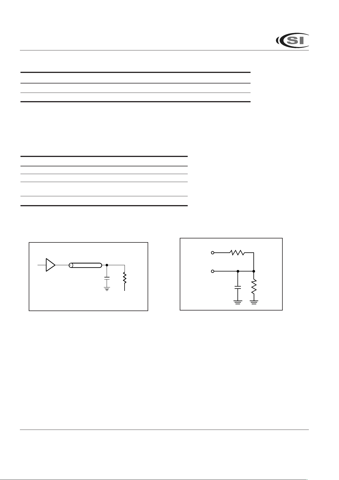
Output Load See Figures 1 and 2
Figure 1
Output
Buffer
Z
O
= 50Ω
1.5V
50Ω
30 pF
317 Ω
5 pF
Including
jig and
scope
351 Ω
OUTPUT
3.3V
Figure 2
AC TEST LOADS

IC61S6432
Integrated Circuit Solution Inc. 9
SSR016-0A 09/13/2001
READ CYCLE SWITCHING CHARACTERISTICS (Over Operating Range)
-200
(1)
-166 -133 -117
Symbol Parameter Min. Max. Min. Max. Min. Max. Min. Max Unit
tKC Cycle Time 5 — 6 — 7.5 — 8.5 — ns
tKH Clock High Time 1.6 — 2.4 — 2.8 — 3 — ns
tKL Clock Low Time 1.6 — 2.4 — 2.8 — 3 — ns
tKQ Clock Access Time — 4 — 5 — 5 — 5 ns
tKQX
(2)
Clock High to Output Invalid 1 — 1.5 — 1.5 — 1.5 — ns
tKQLZ
(2,3)
Clock High to Output Low-Z 0 — 0 — 0 — 0 — ns
tKQHZ
(2,3)
Clock High to Output High-Z 1 3.5 1.5 5 1.5 5 1.5 6 ns
tOEQ Output Enable to Output Valid — 3.5 — 5 — 5 — 5 ns
tOEQX
(2)
Output Disable to Output Invalid 0 — 0 — 0 — 0 — ns
tOELZ
(2,3)
Output Enable to Output Low-Z 0 — 0 — 0 — 0 — ns
tOEHZ
(2,3)
Output Disable to Output High-Z — 3 — 3 — 3 — 4 ns
tAS Address Setup Time 2 — 2.5 — 2.5 — 2.5 — ns
tSS Address Status Setup Time 2 — 2.5 — 2.5 — 2.5 — ns
tWS Write Setup Time 2 — 2.5 — 2.5 — 2.5 — ns
tCES Chip Enable Setup Time 2 — 2.5 — 2.5 — 2.5 — ns
tAVS Address Advance Setup Time 2 — 2.5 — 2.5 — 2.5 — ns
tAH Address Hold Time 0.5 — 0.5 — 0.5 — 0.5 — ns
tSH Address Status Hold Time 0.5 — 0.5 — 0.5 — 0.5 — ns
tWH Write Hold Time 0.5 — 0.5 — 0.5 — 0.5 — ns
tCEH Chip Enable Hold Time 0.5 — 0.5 — 0.5 — 0.5 — ns
tAVH Address Advance Hold Time 0.5 — 0.5 — 0.5 — 0.5 — ns
tCFG
(4)
Configuration Setup 25 — 25 — 30 — 35 — ns
Notes:
1. ADVANCE INFORMATION ONLY.
2. Guaranteed but not 100% tested. This parameter is periodically sampled.
3. Tested with load in Figure 2.
4. Configuration signal MODE is static and must not change during normal operation.

IC61S6432
10 Integrated Circuit Solution Inc.
SSR016-0A 09/13/2001
READ CYCLE SWITCHING CHARACTERISTICS (Over Operating Range) (Continued)
-5 -6 -7 -8
Symbol Parameter Min. Max. Min. Max. Min. Max. Min. Max Unit
tKC Cycle Time 10 — 12 — 13 — 15 — ns
tKH Clock High Time 3.5 — 4 — 6 — 6 — ns
tKL Clock Low Time 3.5 — 4 — 6 — 6 — ns
tKQ Clock Access Time — 5 — 6 — 7 — 8 ns
tKQX
(1)
Clock High to Output Invalid 1.5 — 1.5 — 2 — 2 — ns
tKQLZ
(1,2)
Clock High to Output Low-Z 0 — 0 — 0 — 0 — ns
tKQHZ
(1,2)
Clock High to Output High-Z 1.5 6 1.5 6 2626 ns
tOEQ Output Enable to Output Valid — 5 — 6 — 6 — 6 ns
tOEQX
(1)
Output Disable to Output Invalid 0 — 0 — 0 — 0 — ns
tOELZ
(1,2)
Output Enable to Output Low-Z 0 — 0 — 0 — 0 — ns
tOEHZ
(1,2)
Output Disable to Output High-Z — 4 — 5 — 6 — 6 ns
tAS Address Setup Time 2.5 — 2.5 — 2.5 — 2.5 — ns
tSS Address Status Setup Time 2.5 — 2.5 — 2.5 — 2.5 — ns
tWS Write Setup Time 2.5 — 2.5 — 2.5 — 2.5 — ns
tCES Chip Enable Setup Time 2.5 — 2.5 — 2.5 — 2.5 — ns
tAVS Address Advance Setup Time 2.5 — 2.5 — 2.5 — 2.5 — ns
tAH Address Hold Time 0.5 — 0.5 — 0.5 — 0.5 — ns
tSH Address Status Hold Time 0.5 — 0.5 — 0.5 — 0.5 — ns
tWH Write Hold Time 0.5 — 0.5 — 0.5 — 0.5 — ns
tCEH Chip Enable Hold Time 0.5 — 0.5 — 0.5 — 0.5 — ns
tAVH Address Advance Hold Time 0.5 — 0.5 — 0.5 — 0.5 — ns
tCFG
(3)
Configuration Setup 35 — 45 — 66.7 — 80 — ns
Notes:
1. Guaranteed but not 100% tested. This parameter is periodically sampled.
2. Tested with load in Figure 2.
3. Configuration signal MODE is static and must not change during normal operation.

IC61S6432
Integrated Circuit Solution Inc. 11
SSR016-0A 09/13/2001
READ CYCLE TIMING: PIPELINE
Single Read
High-Z
High-Z
DATA
OUT
DATA
IN
OE
CE3
CE2
CE1
BW4-BW1
BWE
GW
A15-A0
ADV
ADSC
ADSP
CLK
RD1 RD2
1a
2c 2d 3a
Unselected
Burst Read
t
KQX
t
KC
t
KL
t
KH
t
SS
t
SH
t
SS
t
SH
t
AS
t
AH
t
WS
t
WH
t
WS
t
WH
RD3
t
CES
t
CEH
t
CES
t
CEH
t
CES
t
CEH
CE2 and CE3 only sampled with ADSP or ADSC
CE1 Masks ADSP
Unselected with CE2
t
OEQ
t
OEQX
t
OELZ
t
KQLZ
t
KQ
t
OEHZ
t
KQHZ
ADSC initiate read
ADSP is blocked by CE1 inactive
t
AVH
t
AVS
Suspend Burst
Pipelined Read
2a 2b

IC61S6432
12 Integrated Circuit Solution Inc.
SSR016-0A 09/13/2001
WRITE CYCLE SWITCHING CHARACTERISTICS (Over Operating Range)
-200
(1)
-166 -133 -117
Symbol Parameter Min. Max. Min. Max. Min. Max. Min. Max. Unit
tKC Cycle Time 5 — 6 — 7.5 — 8.5 — ns
tKH Clock High Time 1.6 — 2.4 — 2.8 — 3 — ns
tKL Clock Low Time 1.6 — 2.4 — 2.8 — 3 — ns
tAS Address Setup Time 2 — 2.5 — 2.5 — 2.5 — ns
tSS Address Status Setup Time 2 — 2.5 — 2.5 — 2.5 — ns
tWS Write Setup Time 2 — 2.5 — 2.5 — 2.5 — ns
tDS Data In Setup Time 2 — 2.5 — 2.5 — 2.5 — ns
tCES Chip Enable Setup Time 2 — 2.5 — 2.5 — 2.5 — ns
tAVS Address Advance Setup Time 2 — 2.5 — 2.5 — 2.5 — ns
tAH Address Hold Time 0.5 — 0.5 — 0.5 — 0.5 — ns
tSH Address Status Hold Time 0.5 — 0.5 — 0.5 — 0.5 — ns
tDH Data In Hold Time 0.5 — 0.5 — 0.5 — 0.5 — ns
tWH Write Hold Time 0.5 — 0.5 — 0.5 — 0.5 — ns
tCEH Chip Enable Hold Time 0.5 — 0.5 — 0.5 — 0.5 — ns
tAVH Address Advance Hold Time 0.5 — 0.5 — 0.5 — 0.5 — ns
tCFG
(2)
Configuration Setup 25
—
25 — 30 — 35 — ns
-5 -6 -7 -8
Symbol Parameter Min. Max. Min. Max. Min. Max. Min. Max. Unit
tKC Cycle Time 10 — 12 — 13 — 15 — ns
tKH Clock High Time 3.5 — 4 — 6 — 6 — ns
tKL Clock Low Time 3.5 — 4 — 6 — 6 — ns
tAS Address Setup Time 2.5 — 2.5 — 2.5 — 2.5 — ns
tSS Address Status Setup Time 2.5 — 2.5 — 2.5 — 2.5 — ns
tWS Write Setup Time 2.5 — 2.5 — 2.5 — 2.5 — ns
tDS Data In Setup Time 2.5 — 2.5 — 2.5 — 2.5 — ns
tCES Chip Enable Setup Time 2.5 — 2.5 — 2.5 — 2.5 — ns
tAVS Address Advance Setup Time 2.5 — 2.5 — 2.5 — 2.5 — ns
tAH Address Hold Time 0.5 — 0.5 — 0.5 — 0.5 — ns
tSH Address Status Hold Time 0.5 — 0.5 — 0.5 — 0.5 — ns
tDH Data In Hold Time 0.5 — 0.5 — 0.5 — 0.5 — ns
tWH Write Hold Time 0.5 — 0.5 — 0.5 — 0.5 — ns
tCEH Chip Enable Hold Time 0.5 — 0.5 — 0.5 — 0.5 — ns
tAVH Address Advance Hold Time 0.5 — 0.5 — 0.5 — 0.5 — ns
tCFG
(2)
Configuration Setup 35 — 45 — 52 — 60 — ns
Note:
1. ADVANCE INFORMATION ONLY.
2. Configuration signal MODE is static and must not change during normal operation.

IC61S6432
Integrated Circuit Solution Inc. 13
SSR016-0A 09/13/2001
WRITE CYCLE TIMING
Single Write
DATA
OUT
DATA
IN
OE
CE3
CE2
CE1
BW4-BW1
BWE
GW
A15-A0
ADV
ADSC
ADSP
CLK
WR1 WR2
Unselected
Burst Write
t
KC
t
KL
t
KH
t
SS
t
SH
t
AS
t
AH
t
WS
t
WH
t
WS
t
WH
WR3
t
CES
t
CEH
t
CES
t
CEH
t
CES
t
CEH
CE2 and CE3 only sampled with ADSP or ADSC
CE1 Masks ADSP
Unselected with CE2
ADSC initiate Write
ADSP is blocked by CE1 inactive
t
AVH
t
AVS
ADV must be inactive for ADSP Write
WR1 WR2
t
WS
t
WH
WR3
t
WS
t
WH
High-Z
High-Z
1a
3a
t
DS
t
DH
BW4-BW1 only are applied to first cycle of WR2
Write
2c 2d2b2a

IC61S6432
14 Integrated Circuit Solution Inc.
SSR016-0A 09/13/2001
READ/WRITE CYCLE SWITCHING CHARACTERISTICS (Over Operating Range)
-200
(1)
-166 -133 -117
Symbol Parameter Min. Max. Min. Max. Min. Max. Min. Max. Unit
tKC Cycle Time 5 — 6 — 7.5 — 8.5 — ns
tKH Clock High Time 1.6 — 2.4 — 2.8 — 3 — ns
tKL Clock Low Time 1.6 — 2.4 — 2.8 — 3 — ns
tKQ Clock Access Time — 4 — 5 — 5 — 5 ns
tKQX
(2)
Clock High to Output Invalid 1 — 1.5 — 1.5 — 1.5 — ns
tKQLZ
(2,3)
Clock High to Output Low-Z — 0 — 0 — 0 — ns
tKQHZ
(2,3)
Clock High to Output High-Z 1 3.5 1.5 5 1.5 5 1.5 6 ns
tOEQ Output Enable to Output Valid — 3.5 — 5 — 5 — 5 ns
tOEQX
(2)
Output Disable to Output Invalid 0
—
0— 0—0— ns
tOELZ
(2,3)
Output Enable to Output Low-Z 0 — 0 — 0 — 0 — ns
tOEHZ
(2,3)
Output Disable to Output High-Z — 3 — 3 — 3 — 4 ns
tAS Address Setup Time 2 — 2.5 — 2.5 — 2.5 — ns
tSS Address Status Setup Time 2 — 2.5 — 2.5 — 2.5 — ns
tWS Write Setup Time 2 — 2.5 — 2.5 — 2.5 — ns
tCES Chip Enable Setup Time 2 — 2.5 — 2.5 — 2.5 — ns
tAH Address Hold Time 0.5 — 0.5 — 0.5 — 0.5 — ns
tSH Address Status Hold Time 0.5 — 0.5 — 0.5 — 0.5 — ns
tWH Write Hold Time 0.5 — 0.5 — 0.5 — 0.5 — ns
tCEH Chip Enable Hold Time 0.5 — 0.5 — 0.5 — 0.5 — ns
tCFG
(4)
Configuration Setup 25
—
25 — 30 — 35 — ns
Notes:
1. ADVANCE INFORMATION ONLY.
2. Guaranteed but not 100% tested. This parameter is periodically sampled.
3. Tested with load in Figure 2.
4. Configuration signal MODE is static and must not change during normal operation.

IC61S6432
Integrated Circuit Solution Inc. 15
SSR016-0A 09/13/2001
READ/WRITE CYCLE SWITCHING CHARACTERISTICS (Over Operating Range) (Continued)
-5 -6 -7 -8
Symbol Parameter Min. Max. Min. Max. Min. Max. Min. Max. Unit
tKC Cycle Time 10 — 12 — 13 — 15 — ns
tKH Clock High Time 3.5 — 4 — 6 — 6 — ns
tKL Clock Low Time 3.5 — 4 — 6 — 6 — ns
tKQ Clock Access Time — 5 — 6 — 7 — 8 ns
tKQX
(1)
Clock High to Output Invalid 1.5 — 1.5 — 2 — 2 — ns
tKQLZ
(1,2)
Clock High to Output Low-Z 0 — 0 — 0 — 0 — ns
tKQHZ
(1,2)
Clock High to Output High-Z 1.5 6 1.5 6 2626 ns
tOEQ Output Enable to Output Valid — 5 — 6 — 6 — 6 ns
tOEQX
(1)
Output Disable to Output Invalid 0 — 0 — 0 — 0 — ns
tOELZ
(1,2)
Output Enable to Output Low-Z 0 — 0 — 0 — 0 — ns
tOEHZ
(1,2)
Output Disable to Output High-Z — 4 — 5 — 6 — 6 ns
tAS Address Setup Time 2.5 — 2.5 — 2.5 — 2.5 — ns
tSS Address Status Setup Time 2.5 — 2.5 — 2.5 — 2.5 — ns
tWS Write Setup Time 2.5 — 2.5 — 2.5 — 2.5 — ns
tCES Chip Enable Setup Time 2.5 — 2.5 — 2.5 — 2.5 — ns
tAH Address Hold Time 0.5 — 0.5 — 0.5 — 0.5 — ns
tSH Address Status Hold Time 0.5 — 0.5 — 0.5 — 0.5 — ns
tWH Write Hold Time 0.5 — 0.5 — 0.5 — 0.5 — ns
tCEH Chip Enable Hold Time 0.5 — 0.5 — 0.5 — 0.5 — ns
tCFG
(3)
Configuration Setup 35 — 45 — 52 — 60 — ns
Notes:
1. Guaranteed but not 100% tested. This parameter is periodically sampled.
2. Tested with load in Figure 2.
3. Configuration signal MODE is static and must not change during normal operation.
IC61S6432
16 Integrated Circuit Solution Inc.
SSR016-0A 09/13/2001
READ/WRITE CYCLE TIMING: PIPELINE
Single Read
Single Write
High-Z
High-Z
DATA
OUT
DATA
IN
OE
CE3
CE2
CE1
BW4-BW1
BWE
GW
A15-A0
ADV
ADSC
ADSP
CLK
RD1 WR1
WR1
1a
1a
2a 2b 2c 2d
Unselected
Burst Read
t
KQX
t
KC
t
KL
t
KH
t
SS
t
SH
ADSP is blocked by CE1 inactive
t
SS
t
SH
t
AS
t
AH
t
WS
t
WH
t
WS
t
WH
t
WS
t
WH
RD2 RD3
t
CES
t
CEH
t
CES
t
CEH
t
CES
t
CEH
CE2 and CE3 only sampled with ADSP or ADSC
CE1 Masks ADSP
Unselected with CE3
t
OEQ
t
OEQX
t
OELZ
t
KQLZ
t
KQ
t
OEHZ
t
KQX
t
KQHZ
t
DS
t
DH
t
KQHZ

IC61S6432
Integrated Circuit Solution Inc. 17
SSR016-0A 09/13/2001
SNOOZE AND RECOVERY CYCLE SWITCHING CHARACTERISTICS
(1)
(Over Operating
Range)
-200
(2)
-166 -133 -117
Symbol Parameter Min. Max. Min. Max Min. Max. Min. Max. Unit
tKC Cycle Time 5 — 6 — 7.5 — 8.5 — ns
tKH Clock High Time 1.6 — 2.4 — 2.8 — 3 — ns
tKL Clock Low Time 1.6 — 2.4 — 2.8 — 3 — ns
tKQ Clock Access Time — 4 — 5 — 5 — 5 ns
tKQX
(3)
Clock High to Output Invalid 1 — 1.5 — 1.5 — 1.5 — ns
tKQLZ
(3,4)
Clock High to Output Low-Z 0 — 0 — 0 — 0 — ns
tKQHZ
(3,4)
Clock High to Output High-Z 1 3.5 1.5 5 1.5 5 1.5 6 ns
tOEQ Output Enable to Output Valid — 3.5 — 5 — 5 — 5 ns
tOEQX
(3)
Output Disable to Output Invalid 0
—
0— 0—0— ns
tOELZ
(3,4)
Output Enable to Output Low-Z 0 — 0 — 0 — 0 — ns
tOEHZ
(3,4)
Output Disable to Output High-Z — 3 — 3 — 3 — 4 ns
tAS Address Setup Time 2 — 2.5 — 2.5 — 2.5 — ns
tSS Address Status Setup Time 2 — 2.5 — 2.5 — 2.5 — ns
tCES Chip Enable Setup Time 2 — 2.5 — 2.5 — 2.5 — ns
tAH Address Hold Time 2 — 2.5 — 2.5 — 2.5 — ns
tSH Address Status Hold Time 2 — 2.5 — 2.5 — 2.5 — ns
tCEH Chip Enable Hold Time 2 — 2.5 — 2.5 — 2.5 — ns
tZZS
(5)
ZZ Standby — 8 2 — 2 — 2 — cyc
tZZREC
(6)
ZZ Recovery 8 — 2 — 2 — 2 — cyc
Notes:
1. Configuration signal MODE is static and must not change during normal operation.
2. ADVANCE INFORMATION ONLY.
3. Guaranteed but not 100% tested. This parameter is periodically sampled.
4. Tested with load in Figure 2.
5. The assertion of ZZ allows the SRAM to enter a lower power state than when deselected within the time specified. Data
retention is guaranteed when ZZ is asserted and clock remains active.
6. ADSC and ADSP must not be asserted for at least two cycles after leaving ZZ state.
IC61S6432
18 Integrated Circuit Solution Inc.
SSR016-0A 09/13/2001
SNOOZE AND RECOVERY CYCLE SWITCHING CHARACTERISTICS
(1)
(Over Operating
Range) (Continued)
-5 -6 -7 -8
Symbol Parameter Min. Max. Min. Max. Min. Max. Min. Max. Unit
tKC Cycle Time 10 — 12 — 13 — 15 — ns
tKH Clock High Time 3.5 — 4 — 6 — 6 — ns
tKL Clock Low Time 3.5 — 4 — 6 — 6 — ns
tKQ Clock Access Time — 5 — 6 — 7 — 8 ns
tKQX
(2)
Clock High to Output Invalid 1.5 — 1.5 — 2 — 2 — ns
tKQLZ
(2,3)
Clock High to Output Low-Z 0 — 0 — 0 — 0 — ns
tKQHZ
(2,3)
Clock High to Output High-Z 1.5 6 1.5 6 2626 ns
tOEQ Output Enable to Output Valid — 5 — 6 — 6 — 6 ns
tOEQX
(2)
Output Disable to Output Invalid 0 — 0 — 0 — 0 — ns
tOELZ
(2,3)
Output Enable to Output Low-Z 0 — 0 — 0 — 0 — ns
tOEHZ
(2,3)
Output Disable to Output High-Z — 4 — 5 — 6 — 6 ns
tAS Address Setup Time 2.5 — 2.5 — 2.5 — 2.5 — ns
tSS Address Status Setup Time 2.5 — 2.5 — 2.5 — 2.5 — ns
tCES Chip Enable Setup Time 2.5 — 2.5 — 2.5 — 2.5 — ns
tAH Address Hold Time 2.5 — 2.5 — 2.5 — 2.5 — ns
tSH Address Status Hold Time 2.5 — 2.5 — 2.5 — 2.5 — ns
tCEH Chip Enable Hold Time 2.5 — 2.5 — 2.5 — 2.5 — ns
tZZS
(4)
ZZ Standby 2 — 2 — 2 — 2 — cyc
tZZREC
(5)
ZZ Recovery 2 — 2 — 2 — 2 — cyc
Notes:
1. Configuration signal MODE is static and must not change during normal operation.
2. Guaranteed but not 100% tested. This parameter is periodically sampled.
3. Tested with load in Figure 2.
4. The assertion of ZZ allows the SRAM to enter a lower power state than when deselected within the time specified. Data
retention is guaranteed when ZZ is asserted and clock remains active.
5. ADSC and ADSP must not be asserted for at least two cycles after leaving ZZ state.

IC61S6432
Integrated Circuit Solution Inc. 19
SSR016-0A 09/13/2001
SNOOZE AND RECOVERY CYCLE TIMING
Single Read
High-Z
High-Z
DATA
OUT
DATA
IN
OE
CE3
CE2
CE1
BW4-BW1
BWE
GW
A15-A0
ADV
ADSC
ADSP
CLK
RD1
1a
Read
Snooze with Data Retention
t
KC
t
KL
t
KH
t
SS
t
SH
t
AS
t
AH
RD2
t
CES
t
CEH
t
CES
t
CEH
t
CES
t
CEH
t
OEQ
t
OEQX
t
OELZ
t
KQLZ
t
KQ
t
OEHZ
t
KQX
t
KQHZ
ZZ
t
ZZS
t
ZZREC

IC61S6432
20 Integrated Circuit Solution Inc.
SSR016-0A 09/13/2001
ORDERING INFORMATION
Commercial Range: 0°C to +70°C
Frequency (MHz) Order Part Number Package
200 IC61S6432-200TQ 14*20*1.4mm LQFP
IC61S6432-200PQ 14*20*2.7mm PQFP
166 IC61S6432-166TQ 14*20*1.4mm LQFP
IC61S6432-166PQ 14*20*2.7mm PQFP
133 IC61S6432-133TQ 14*20*1.4mm LQFP
IC61S6432-133PQ 14*20*2.7mm PQFP
117 IC61S6432-117TQ 14*20*1.4mm LQFP
IC61S6432-117PQ 14*20*2.7mm PQFP
100 IC61S6432-5TQ 14*20*1.4mm LQFP
IC61S6432-5PQ 14*20*2.7mm PQFP
83 IC61S6432-6TQ 14*20*1.4mm LQFP
IC61S6432-6PQ 14*20*2.7mm PQFP
75 IC61S6432-7TQ 14*20*1.4mm LQFP
IC61S6432-7PQ 14*20*2.7mm PQFP
66 IC61S6432-8TQ 14*20*1.4mm LQFP
IC61S6432-8PQ 14*20*2.7mm PQFP
ORDERING INFORMATION
Industrial Range: –40°C to +85°C
Frequency (MHz) Order Part Number Package
117 IC61S6432-117TQI 14*20*1.4mm LQFP
IC61S6432-117PQI 14*20*2.7mm PQFP
100 IC61S6432-5TQI 14*20*1.4mm LQFP
IC61S6432-5PQI 14*20*2.7mm PQFP
83 IC61S6432-6TQI 14*20*1.4mm LQFP
IC61S6432-6PQI 14*20*2.7mm PQFP
75 IC61S6432-7TQI 14*20*1.4mm LQFP
IC61S6432-7PQI 14*20*2.7mm PQFP
66 IC61S6432-8TQI 14*20*1.4mm LQFP
IC61S6432-8PQI 14*20*2.7mm PQFP

IC61S6432
Integrated Circuit Solution Inc. 21
SSR016-0A 09/13/2001
Integrated Circuit Solution Inc.
HEADQUARTER:
NO.2, TECHNOLOGY RD. V, SCIENCE-BASED INDUSTRIAL PARK,
HSIN-CHU, TAIWAN, R.O.C.
TEL: 886-3-5780333
Fax: 886-3-5783000
BRANCH OFFICE:
7F, NO. 106, SEC. 1, HSIN-TAI 5TH ROAD,
HSICHIH TAIPEI COUNTY, TAIWAN, R.O.C.
TEL: 886-2-26962140
FAX: 886-2-26962252
http://www.icsi.com.tw
 Loading...