

Page 1
查询ICS501供应商
ICS501B
LOCO™ PLL CLOCK MULTIPLIER
Description
The ICS501B LOCO
generate a high-quality clock output from a lower
frequency crystal or clock input. The name LOCO
stands for Low Cost Oscillator, as it is designed to
replace crystal oscillators in most electronic systems.
Using Phase-Locked Loop (PLL) techniques, the
device uses a standard fundamental mode,
inexpensive crystal to produce output clocks up to 20
MHz.
Stored in the chip’s ROM is the ability to generate nine
different multiplication factors, allowing one chip to
output many common frequencies (see table on page
2).
The device also has an output enable pin which
tri-states the clock output when the OE pin is taken low.
This product is intended for clock generation. It has low
output jitter (variation in the output period), but input to
output skew and jitter are not defined or guaranteed.
For applications which require defined input to output
skew, use the ICS570B.
TM
is the most cost effective way to
Features
• Packaged as 8 pin SOIC or die
• Available in Pb (lead) free package
• ICS’ lowest cost PLL clock
• Zero ppm multiplication error
• Input crystal frequency of 5 MHz
• Input clock frequency of 5 MHz
• Output clock frequencies up to 15 MHz
• Extremely low jitter of 25 ps (one sigma)
• Compatible with popular CPUs
• Duty cycle of 45/55 up to 20 MHz
• Nine selectable frequencies
• Operating voltage of 3.3 V or 5.5 V
• Tri-state output for board level testing
• 25 mA drive capability at TTL levels
• Ideal for oscillator replacement
• Industrial temperature version available
• Advanced, low-power CMOS process
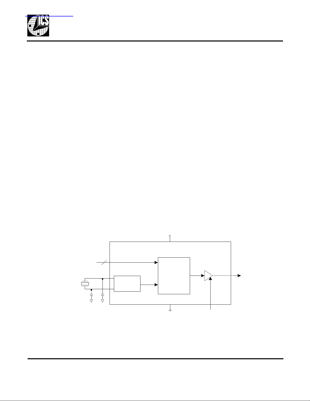
Block Diagram
Crystal or
Clock input
Optional crystal capacitors
S1:0
X1/ICLK
X2
2
Crystal
Oscillator
VDD
PLL Clock
Multiplier
Circuitry
and ROM
GND
CLK
OE
MDS 501B C 1 Revision 120704
Integrated Circuit Systems ● 525 Race Street, San Jose, CA 95126 ● tel (408) 297-1201 ● www.icst.com
Page 2
LOCO™ PLL Clock Multiplier
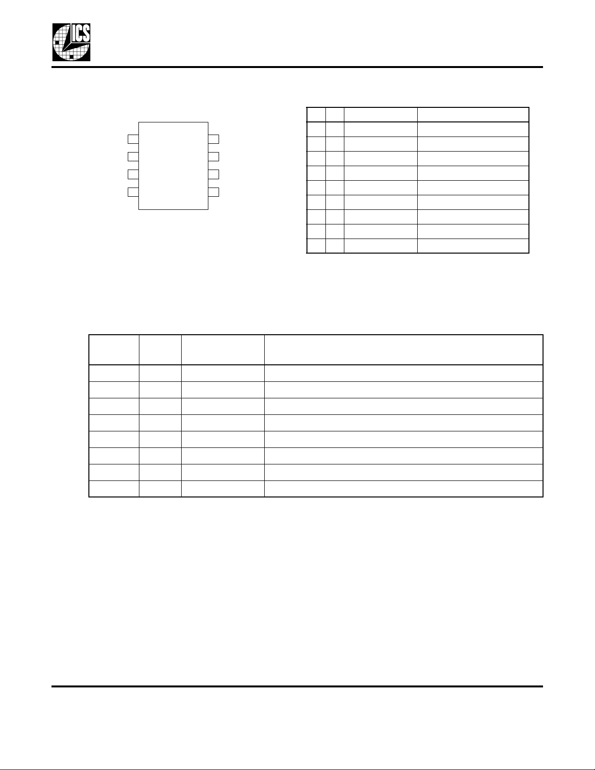
Pin Assignment Clock Output Table
S1 S0 CLK Minimum Input
0 0 4X input 0.5 MHz
X1/ICLK
VDD
GND
S1
2
3
4
8 Pin (150 mil) SOIC
8
X21
OE
7
6
S0
5
CLK
0 M 5.3125X input 1 MHz
0 1 5X input 0.5 MHz 5
M 0 6.25X input 0.5 MHz
M M 2X input 1 MHz
M 1 3.125X input 1 MHz
1 0 6X input 0.5MHz
1 M 3X input 0.5MHz
1 1 8X input 0.5MHz
0 = connect directly to ground
1 = connect directly to VDD
M = leave unconnected (floating)
ICS501B
Pin Descriptions
Pin
Number
1 XI/ICLK Input Crystal connection or clock input.
2 VDD Power Connect to +3.3 V or +5 V.
3 GND Power Connect to ground.
4 S1 Tri-level Iinput Select 1 for output clock. Connect to GND or VDD or float.
5 CLK Output Clock output per table above.
6 S0 Tri-level Input Select 0 for output clock. Connect to GND or VDD or float.
7 OE Input Output enable. Tri-states CLK output when low. Internal pull-up.
8 X2 Output Crystal connection. Leave unconnected for clock input.
Pin
Name
Pin
Type
Pin Description
MDS 501B C 2 Revision 120704
Integrated Circuit Systems ● 525 Race Street, San Jose, CA 95126 ● tel (408) 297-1201 ● www.icst.com
Page 3

ICS501B
LOCO™ PLL Clock Multiplier
External Components
Decoupling Capacitor
As with any high-performance mixed-signal IC, the
ICS501B must be isolated from system power supply
noise to perform optimally.
A decoupling capacitor of 0.01µF must be connected
between VDD and the GND. It must be connected
close to the ICS501B to minimize lead inductance. No
external power supply filtering is required for the
ICS501B.
Series Termination Resistor
A 33Ω terminating resistor can be used next to the CLK
pin for trace lengths over one inch.
Crystal Load Capacitors
The total on-chip capacitance is approximately 12 pF. A
parallel resonant, fundamental mode crystal should be
used. The device crystal connections should include
pads for small capacitors from X1 to ground and from
X2 to ground. These capacitors are used to adjust the
stray capacitance of the board to match the nominally
required crystal load capacitance. Because load
capacitance can only be increased in this trimming
process, it is important to keep stray capacitance to a
minimum by using very short PCB traces (and no vias)
between the crystal and device. Crystal capacitors, if
needed, must be connected from each of the pins X1
and X2 to ground.
The value (in pF) of these crystal caps should equal
(C
-12 pF)*2. In this equation, CL= crystal load
L
capacitance in pF. Example: For a crystal with a 16 pF
load capacitance, each crystal capacitor would be 8 pF
[(16-12) x 2] = 8.
MDS 501B C 3 Revision 120704
Integrated Circuit Systems
● 525 Race Street, San Jose, CA 95126 ● tel (408) 297-1201 ● www.icst.com
Page 4
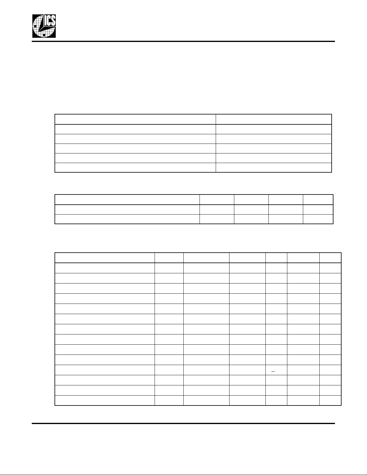
Absolute Maximum Ratings
Stresses above the ratings listed below can cause permanent damage to the ICS501B. These ratings,
which are standard values for ICS commercially rated parts, are stress ratings only. Functional operation of
the device at these or any other conditions above those indicated in the operational sections of the
specifications is not implied. Exposure to absolute maximum rating conditions for extended periods can
affect product reliability. Electrical parameters are guaranteed only over the recommended operating
temperature range.
Item Rating
Supply Voltage, VDD 7 V
All Inputs and Outputs -0.5 V to VDD+0.5 V
Ambient Operating Temperature -40 to +85°C
Storage Temperature -65 to +150°C
Soldering Temperature 260°C
Recommended Operation Conditions
ICS501B
LOCO™ PLL Clock Multiplier
Parameter Min. Typ. Max. Units
Ambient Operating Temperature 0 +70 °C
Power Supply Voltage (measured in respect to GND) +3.14 +5.25 V
DC Electrical Characteristics
VDD=5.0 V ±5% , Ambient temperature 0 to +70°C, unless stated otherwise
Parameter Symbol Conditions Min. Typ. Max. Units
Operating Voltage VDD 3.14 5.25 V
Input High Voltage, ICLK only V
Input Low Voltage, ICLK only V
Input High Voltage V
Input Low Voltage V
Input High Voltage V
Input Low Voltage V
Output High Voltage V
Output Low Voltage V
IDD Operating Supply Current No load 20 mA
Short Circuit Current CLK output +
On-Chip Pull-up Resistor Pin 7 270 kΩ
IH
IL
IH
IL
IH
IL
OH
OL
ICLK (pin 1) (VDD/2)+1 V
ICLK (pin 1) (VDD/2)-1 V
OE (pin 7) 2.0 V
OE (pin 7) 0.8 V
S0, S1 VDD-0.5 V
S0, S1 0.5 V
I
= -25 mA 2.4 V
OH
IOL = 25 mA 0.4 V
70 mA
Input Capacitance, S1, S0, and OE Pins 4, 6, 7 4 pF
Nominal Output Impedance 20 Ω
MDS 501B C 4 Revision 120704
Integrated Circuit Systems
● 525 Race Street, San Jose, CA 95126 ● tel (408) 297-1201 ● www.icst.com
Page 5
AC Electrical Characteristics
VDD = 5.0 V ±5%, Ambient Temperature 0 to +70° C, unless stated otherwise
Parameter Symbol Conditions Min. Typ. Max. Units
Input Frequency, crystal input F
Input Frequency, clock input F
Output Frequency, VDD = 5.0 V ±5% F
Output Frequency, VDD = 3.3 V ±5% F
Output Clock Rise Time t
Output Clock Fall Time t
Output Clock Duty Cycle t
PLL Bandwidth 10 kHz
Output Enable Time, OE high to
output on
Output Disable Time, OE low to
tri-state
Absolute Clock Period Jitter t
One Sigma Clock Period Jitter t
Note 1: Measured with 15 pF load.
IN
IN
OUT
OUT
OR
OF
OD
ja
js
ICS501B
LOCO™ PLL Clock Multiplier
7.5 MHz
0.5 7.5 MHz
0°C to +70°C4 15MHz
-40°C to +85°C4 15MHz
0°C to +70°C4 15MHz
-40°C to +85°C4 15MHz
0.8 to 2.0 V, Note 1 1 ns
2.0 to 8.0 V, Note 1 1 ns
1.5 V, up to 25 MHz 45 49-51 55 %
50 ns
50 ns
Deviation from
mean, Note 1
Note 1 25 ps
+70 ps
MDS 501B C 5 Revision 120704
Integrated Circuit Systems
● 525 Race Street, San Jose, CA 95126 ● tel (408) 297-1201 ● www.icst.com
Page 6
ICS501B
LOCO™ PLL Clock Multiplier
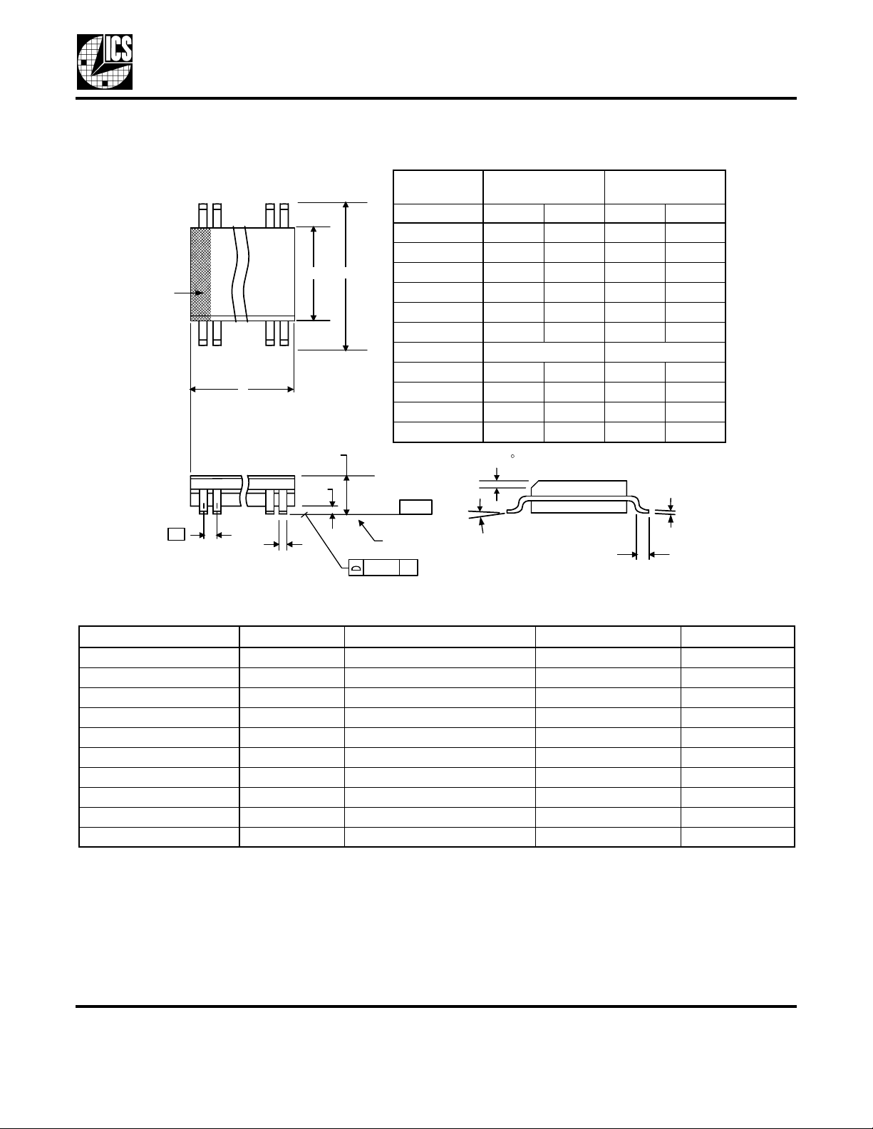
Package Outline and Package Dimensions (8-pin SOIC, 150 Mil. Narrow Body)
Package dimensions are kept current with JEDEC Publication No. 95
Millimeters Inches
8
Symbol MinMaxMinMax
A 1.35 1.75 .0532 .0688
A1 0.10 0.25 .0040 .0098
INDEX
AREA
1 2
E
H
D
A
B 0.33 0.51 .013 .020
C 0.19 0.25 .0075 .0098
D 4.80 5.00 .1890 .1968
E 3.80 4.00 .1497 .1574
e 1.27 BASIC 0.050 BASIC
H 5.80 6.20 .2284 .2440
h 0.25 0.50 .010 .020
L 0.40 1.27 .016 .050
α 0° 8° 0° 8°
h x 45
A1
- C -
e
B
SEATING
.10 (.004)
PLANE
C
L
C
Ordering Information
Part / Order Number Marking Shipping Packaging Package Temperature
ICS501BM 501BM Tubes 8-pin SOIC 0 to +70° C
ICS501BMT 501BM Tape and Reel 8-pin SOIC 0 to +70° C
ICS501BMI 501BMI Tubes 8-pin SOIC -40 to +85° C
ICS501BMIT 501BMI Tape and Reel 8-pin SOIC -40 to +85° C
ICS501BMLF 501BML Tubes 8-pin SOIC 0 to +70° C
ICS501BMLFT 501BML Tape and Reel 8-pin SOIC 0 to +70° C
ICS501BMILF 501BMIL Tubes 8-pin SOIC -40 to +85° C
ICS501BMILFT 501BMIL Tape and Reel 8-pin SOIC -40 to +85° C
ICS501-DWF - Die on uncut, probed wafers 0 to +70° C
ICS501-DPK - Tested die in waffle pack 0 to +70° C
“LF” denotes Pb (lead) free package.
While the information presented herein has been checked for both accuracy and reliability, Integrated Circuit Systems (ICS)
assumes no responsibility for either its use or for the infringement of any patents or other rights of third parties, which would
result from its use. No other circuits, patents, or licenses are implied. This product is intended for use in normal commercial
applications. Any other applications such as those requiring extended temperature range, high reliability, or other extraordinary
environmental requirements are not recommended without additional processing by ICS. ICS reserves the right to change any
circuitry or specifications without notice. ICS does not authorize or warrant any ICS product for use in life support devices or
critical medical instruments.
MDS 501B C 6 Revision 120704
Integrated Circuit Systems
● 525 Race Street, San Jose, CA 95126 ● tel (408) 297-1201 ● www.icst.com
 Loading...