

ICP DAS ZBUPS0001 User Manual

Product #:ZB-UPS01
ZB-UPS01
ZigBee T ransceiver Module
User Manual
Version 0.9
Confidential Page 1/14
Doc. #: ZB-UPS01 Reference Note <Rev. 0.9>

Product #:ZB-UPS01
TABLE OF CONTENTS
1 GENERAL INFORMATION ………………….……………..…….…3
2 POWER SAVING MODES …………………….……….…………….4
3 CONNECTORS PIN CONFIGURATION … …….….….….……….5
4 ELECTRICAL SPECIFICATIONS ……………..…………………...6
5 DESIGN GUIDE TO AVOID RF INTERFERENCE …………….....7
6 RF PERFORMANCE TEST DATA …………………….….…….…..10
7 REFERENCE REFLOW TEMPETURE CURVE…………………..11
8 REFERENCE DOCUMENTS………..…………………..…………...11
Confidential Page 2/14
Doc. #: ZB-UPS01 Reference Note <Rev. 0.9>

Product #:ZB-UPS01
Revised Date: Apr.14, 2010
1. GENERAL INFORMATION
The ZB-UPS01 is a miniature 2.4 GHz Direct Sequence Spread Spectrum 802.15.4 transceiver. It
includes all RF hardware and a micro-controller to manage the communications link. The
micro-controller manages all communications task including configuration, data packaging, and
clear channel selection. The result is a complete wireless data communications solution.
The ZB-UPS01 package is unique because of its small form factor (32 x 23 mm2), It has an
on-board chip antenna and the availability of external dipole antenna I-PEX connector. No
competitive products can offer a solution as flexible, convenient, and easy to integrate.
Models
• ZB-UPS01: Includes PA/LNA, on-board chip antenna, MCU SiliconLabs C8051F340
Features
• 32 x 23 mm2 PCBA package with 2 connectors
• Utilizes globally available 2.4 GHz ISM band
• Programmable Transmit Power Output, max. 9dBm.
• Complete IEEE 802.15.4 Spec. compliant.
• Typical Receiver Sensitivity –101dBm.
• Typical Data Rate 250Kbps.
• Multiple Low Power Operating modes
• Meet RoHS Requirement
Confidential Page 3/14
Doc. #: ZB-UPS01 Reference Note <Rev. 0.9>

Product #:ZB-UPS01
2. POWER SAVING MODES
The ZB-UPS01 includes several low power operating modes to permit the most efficient use of the
available power. Below are descriptions of the available selections.
ACTIVE: In Active Mode, all ZB-UPS01 circuits are powered and available for immediate action.
This includes the RF receiver which actively monitors the air for an incoming communications
request. Two sub-modes are classified as TX-ACTIVE and RX-ACTIVE. The current
consumption of TX-ACTIVE is 44 mA while RX-ACTIVE is 38 mA.
Confidential Page 4/14
Doc. #: ZB-UPS01 Reference Note <Rev. 0.9>
Product #:ZB-UPS01
3. CONNECTORS PIN CONFIGURATION
ZB-UPS01/ZB-UPH01 uses Silicon-Lab C8051F340 as MCU. It is an 8051 base MCU and
reserves 10 GPIO pins for external controlling by application. Each pin can be a general I/O pin
and programmed it by user directly. Furthermore, most of these pins can be used as special purpose
function. Thereof TX, RX pins can be programmed as UART for data communication. For
example, user is easy to connect these pins with RS485 transceivers such as 75176, MAX485.
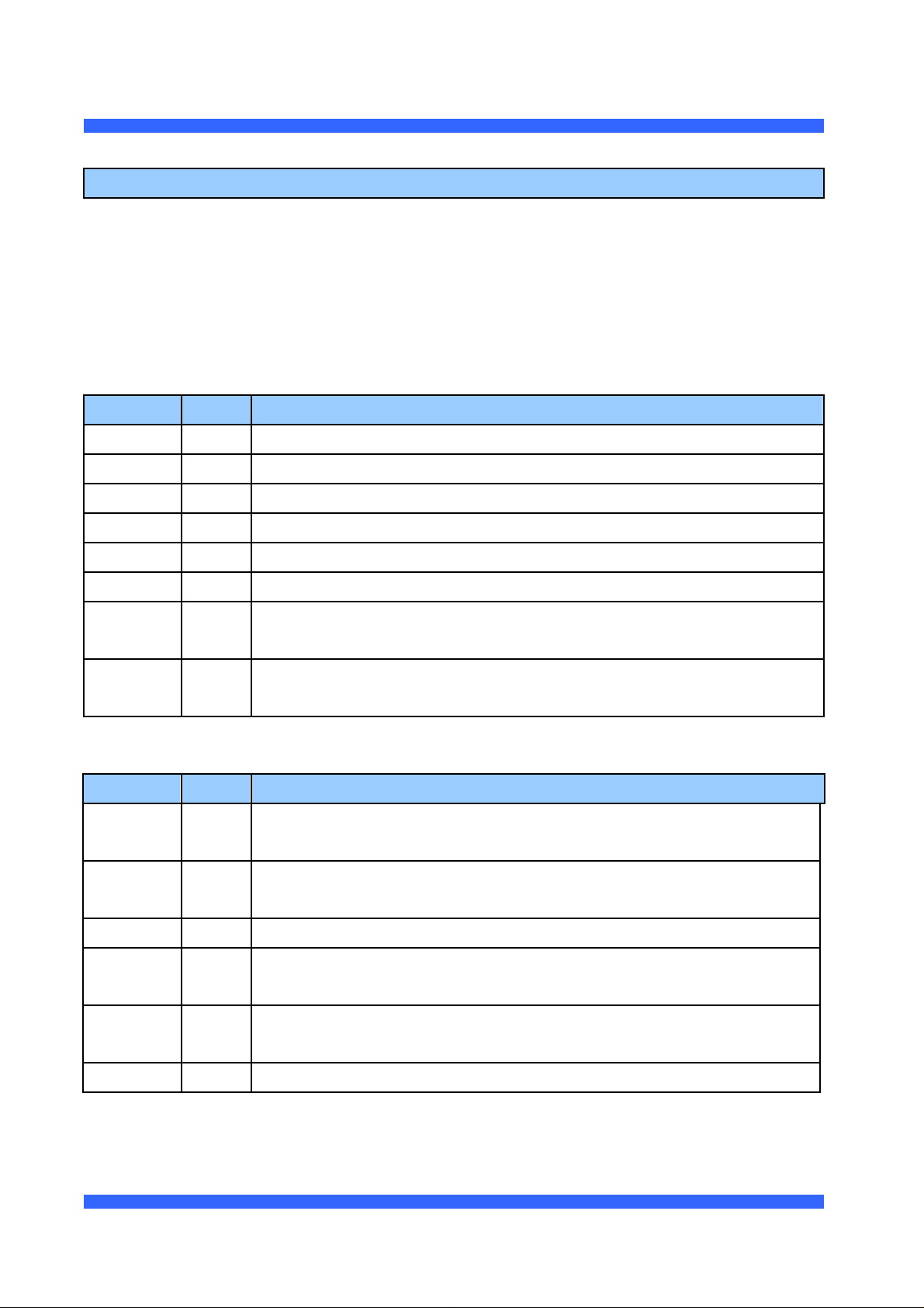
J1 Pin Configuration
Signal Pin Description
C2CK 1 Clock signal for the C2 Debug Interface.
C2D 2 Bi-directional data signal for the C2 Debug Interface.
VCC 3 3.3 Volt power for the ZB-UPS01
TX 4 GPIO, also used as UART TX.
GND 5 Ground
RX 6 GPIO, also used as UART RX.
GPIO1 7 Bidirectional input/output Pin. It also can be programmed as analog to
digital converter (ADC1)
GPIO2 8 Bidirectional input/output Pin. It also can be programmed as analog to
digital converter (ADC2)
J2 Pin Configuration
Signal Pin Description
GPIO3 1 Bidirectional input/output Pin. It also can be programmed as analog to
digital converter (ADC3)
GPIO4 2 Bidirectional input/output Pin. It also can be programmed as analog to
digital converter (ADC4)
GPIO5 3 Bidirectional input/output Pin.
GPIO6 4 Bidirectional input/output Pin. It also can be programmed as analog to
digital converter (ADC5)
GPIO7 5 Bidirectional input/output Pin. It also can be programmed as analog to
digital converter (ADC6)
GPIO8 6 Bidirectional input/output Pin.
Confidential Page 5/14
Doc. #: ZB-UPS01 Reference Note <Rev. 0.9>
 Loading...