

Page 1
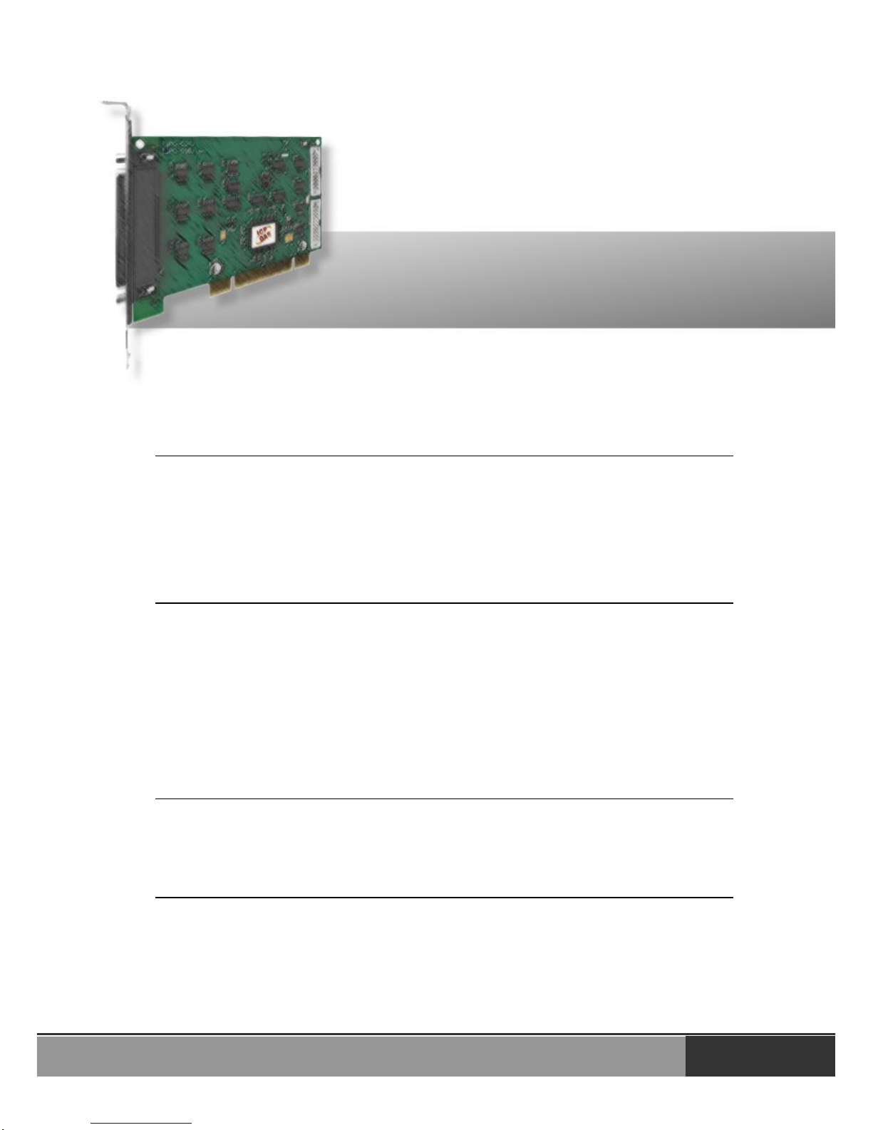
PIO/PEX-D24/D56 Series User Manual (Ver.3.1, Mar. 2015, PMH-005-31) 1
Warranty
All products manufactured by ICP DAS are warranted against defective
materials for a period of one year from the date of delivery to the original
purchaser.
Warning
ICP DAS assumes no liability for damages consequent to the use of this product.
ICP DAS reserves the right to change this manual at any time without notice.
The information furnished by ICP DAS is believed to be accurate and reliable.
However, no responsibility is assumed by ICP DAS for its use, nor for any
infringements of patents or other rights of third parties resulting from its use.
Copyright
Copyright © 2010 by ICP DAS. All rights are reserved.
Trademark
Names are used for identification only and may be registered trademarks of their
respective companies.
PEX-D24/D56
PIO-D24/D56
PIO-D24U/D56U
Version 3.1
Mar. 2015
User Manual
Page 2

PIO/PEX-D24/D56 Series User Manual (Ver.3.1, Mar. 2015, PMH-005-31) 2
Tables of Contents
1. INTRODUCTION .................................................................................................................. 3
1.1 SPECIFICATIONS .............................................................................................................. 4
1.1.1 PIO-D24/D24U/D56/D56U ........................................................................................ 4
1.1.2 PEX-D24/D56 ........................................................................................................... 5
1.2 FEATURES ....................................................................................................................... 6
1.3 PRODUCT CHECK LIST ..................................................................................................... 6
2. HARDWARE CONFIGURATION ......................................................................................... 7
2.1 BOARD LAYOUT ............................................................................................................... 7
2.2 I/O PORT LOCATION ........................................................................................................ 8
2.3 CARD ID SWITCH ............................................................................................................. 9
2.4 PIN ASSIGNMENTS ......................................................................................................... 10
2.5 ENABLE I/O OPERATION ................................................................................................. 13
2.5.1 D/I/O Port Architecture ............................................................................................ 14
2.5.2 D/I Port Architecture ................................................................................................ 15
2.5.3 D/O Port Architecture .............................................................................................. 16
2.6 INTERRUPT OPERATION ................................................................................................. 17
2.7 DAUGHTER BOARDS ...................................................................................................... 19
2.7.1 DB-37 .................................................................................................................... 19
2.7.2 DN-37 and DN-50 ................................................................................................. 19
2.7.3 DB-8125 ................................................................................................................ 20
2.7.4 ADP-20/PCI ............................................................................................................ 20
2.7.5 DB-24P, DB-24PD Isolated Input Board ............................................................... 21
2.7.6 DB-24R, DB-24RD Relay Board ........................................................................... 22
2.7.7 DB-24PR, DB-24POR, DB-24C ............................................................................. 23
2.7.8 Daughter Board Comparison Table ....................................................................... 24
3. I/O CONTROL REGISTER ................................................................................................ 25
3.1 HOW TO FIND THE I/O ADDRESS .......................................................................................... 25
3.2 THE ASSIGNMENT OF I/O ADDRESSES .................................................................................. 28
3.3 THE I/O ADDRESS MAP ....................................................................................................... 30
3.3.1 RESET\ Control Register ........................................................................................ 31
3.3.2 AUX Control Register .............................................................................................. 31
3.3.3 AUX Data Register ................................................................................................... 31
3.3.4 INT Mask Control Register...................................................................................... 32
3.3.5 Aux Status Register ................................................................................................ 32
3.3.6 Read Card ID Register............................................................................................. 32
3.3.7 I/O Selection Control Register ................................................................................ 33
3.3.8 Interrupt Polarity Control Register .......................................................................... 33
3.3.9 Read/Write 8-bit data Register ............................................................................... 34
4. SOFTWARE INSTALLATION ............................................................................................. 35
4.1 SOFTWARE INSTALLING PROCEDURE .............................................................................. 35
4.2 PNP DRIVER INSTALLATION ............................................................................................ 36
4.3 CONFIRM THE SUCCESSFUL INSTALLATION ..................................................................... 37
5. DEMO PROGRAMS FOR WINDOWS ................................................................................ 38
APPENDIX ................................................................................................................................... 39
APPENDIX A. RELATED DOS SOFTWARE .................................................................................... 39
A1. Where is the related software ................................................................................ 39
A2. DOS LIB Functions ................................................................................................ 40
Page 3
PIO/PEX-D24/D56 Series User Manual (Ver.3.1, Mar. 2015, PMH-005-31) 3
1. Introduction
The PIO-D24U/D56U and PEX-D24/D56 card is the new generation product that
ICP DAS provides to meet RoHS compliance requirement. The new PIOD24U/D56U card is designed as a drop-in replacement for the PIO-D24/D56,
and users can replace the PIO-D24/D56 by the PIO-D24U/D56U and PEXD24/D56 directly without software/driver modification.
The PIO-D24U/D56U universal PCI card supports 3.3 V/5 V PCI bus while the
PEX-D24/D56 supports PCI Express bus. The PIO-D24/D56 and PEX-D24/D56
series consists of three 8-bit bi-direction ports. The 8-bit ports are named as port
A (PA), port B (PB) and port C (PC) respectively. All ports are configured as
inputs upon power-up or reset. In addition, the PIO-D56/D56U and PEX-D56
provides additional 16-bit digital inputs and 16-bit digital outputs.
The PIO-D24U/D56U and PEX-D24/D56 has a Card ID switch with which users
can recognize the board by the ID via software when using two or more PIOD24U/56U and PEX-D24/D56 cards in one computer.
These cards support various OS versions, such as Linux, DOS, Windows
98/NT/2000 and 32/64-bit Windows 8/7/Vista/2003/XP. DLL and Active X control
together with various language sample program based on Turbo C++, Borland
c++, Microsoft C++, Visual C++, Borland Delphi, Borland C++ Builder, Visual
Basic, C#.NET, Visual Basic.NET and LabVIEW are provided in order to help
users to quickly and easily develop their own applications.
Page 4
PIO/PEX-D24/D56 Series User Manual (Ver.3.1, Mar. 2015, PMH-005-31) 4
1.1 Specifications
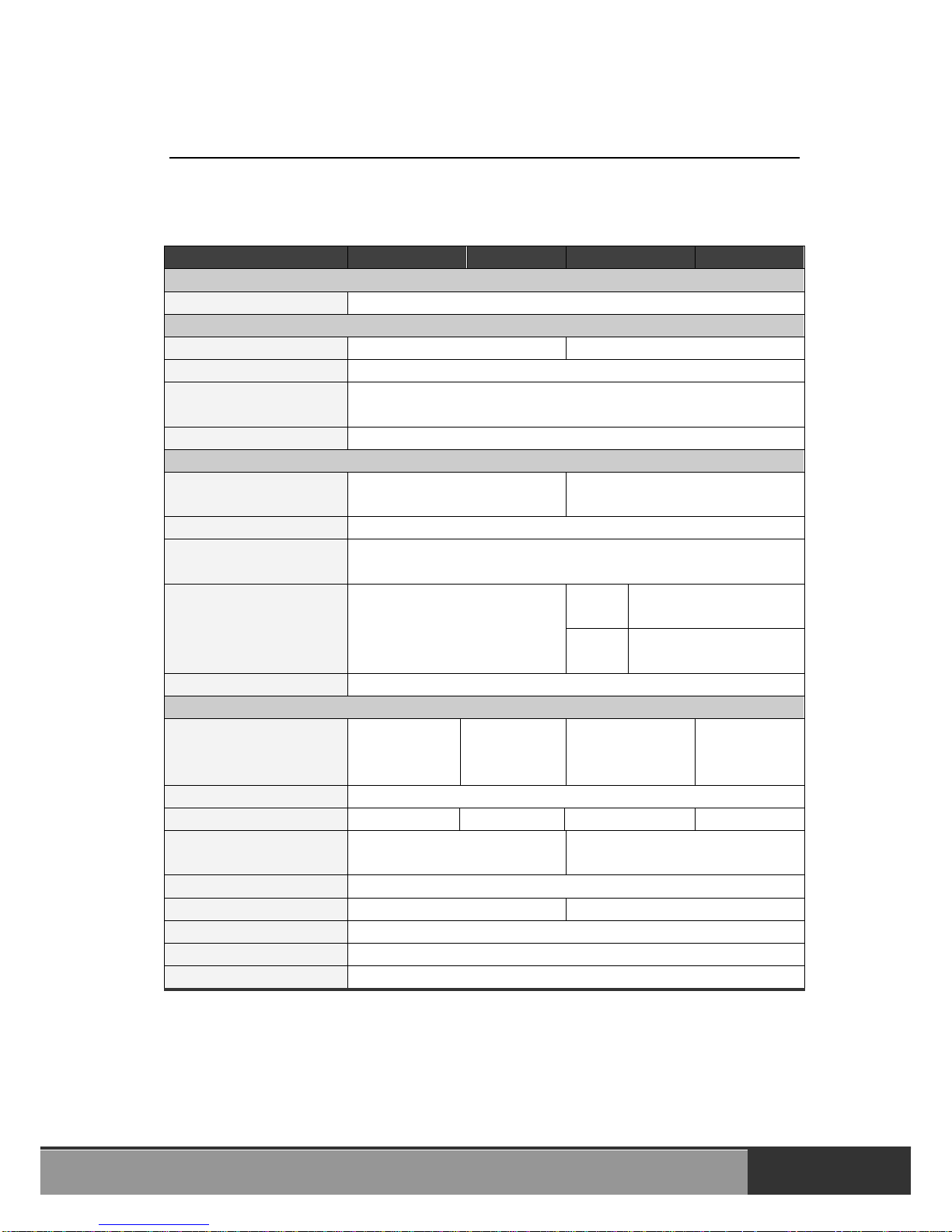
1.1.1 PIO-D24/D24U/D56/D56U
Models
PIO-D24
PIO-D24U
PIO-D56
PIO-D56U
Programmable Digital I/O
Channels
24
Digital Input
Digital Input Channels
-
16
Compatibility
5 V/TTL
Input Voltage
Logic 0: 0.8 V max.
Logic 1: 2.0 V min.
Response Speed
1 MHz
Digital Output
Digital Output
Channels
-
16
Compatibility
5 V/TTL
Output Voltage
Logic 0: 0.4 V max.
Logic 1: 2.4 V min.
Output Capability
Sink: 64 mA @ 0.8 V
Source: 32 mA @ 2.0 V
CON1
Sink: 2.4 mA @ 0.8 V
Source: 0.8 mA @ 2.0 V
CON3
Sink: 64 mA @ 0.8 V
Source: 32 mA @ 2.0 V
Response Speed
1 MHz
General
Bus Type
5 V PCI,
32-bit, 33 MHz
3.3 V/5 V
Universal PCI,
32-bit, 33 MHz
5 V PCI,
32-bit, 33 MHz
3.3 V/5 V
Universal PCI,
32-bit, 33 MHz
Data Bus
8-bit
Card ID
No
Yes(4-bit)
No
Yes(4-bit)
I/O Connector
Female DB37 x 1
Female DB37 x 1
20-pin box header x 2
Dimensions (L x W x D)
143 mm x 105 mm x 22 mm
Power Consumption
420 mA @ +5 V
580 mA @ +5 V
Operating Temperature
0 ~ 60 °C
Storage Temperature
-20 ~ 70 °C
Humidity
5 ~ 85% RH, non-condensing
Page 5
PIO/PEX-D24/D56 Series User Manual (Ver.3.1, Mar. 2015, PMH-005-31) 5
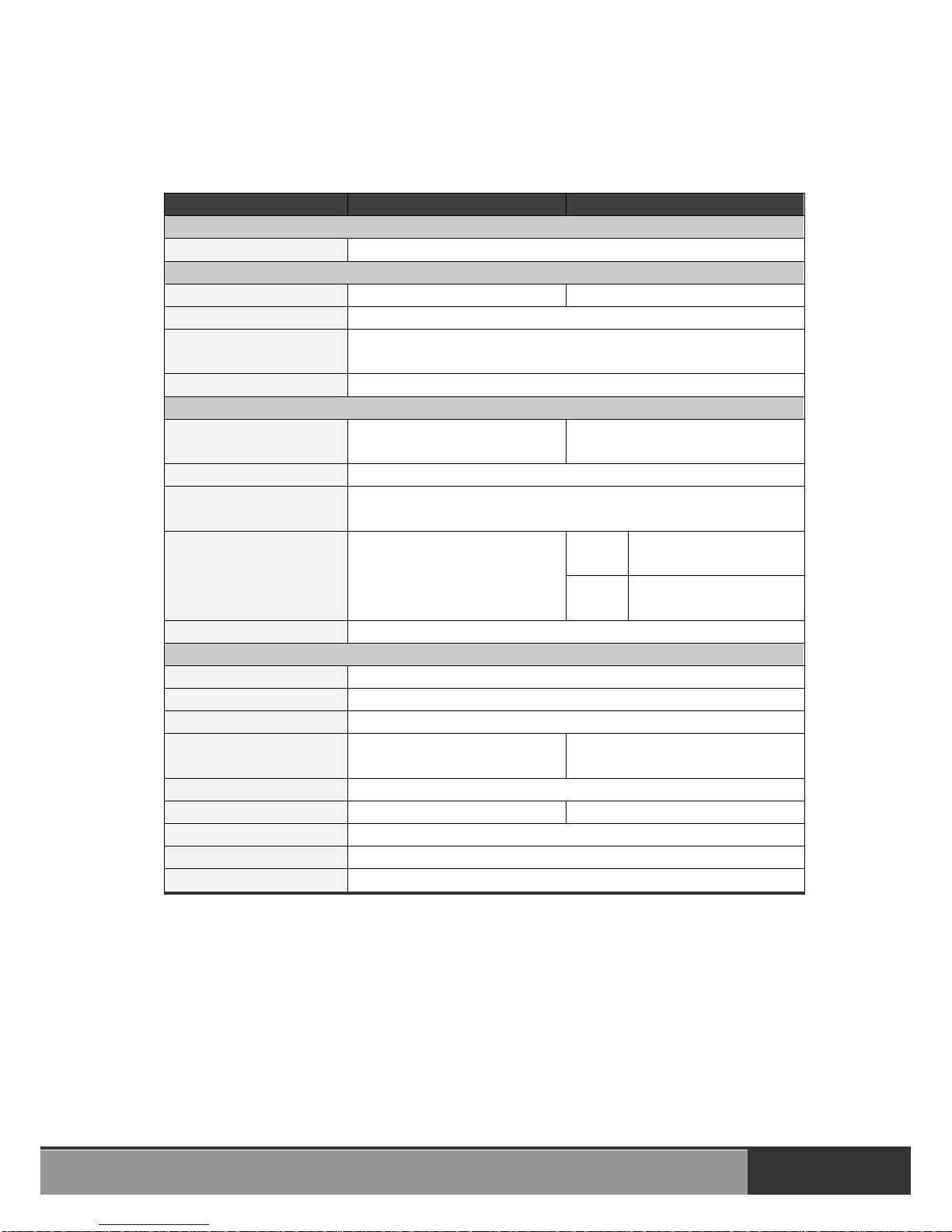
1.1.2 PEX-D24/D56
Models
PEX-D24
PEX-D56
Programmable Digital I/O
Channels
24
Digital Input
Digital Input Channels
-
16
Compatibility
5 V/TTL
Input Voltage
Logic 0: 0.8 V max.
Logic 1: 2.0 V min.
Response Speed
500 kHz
Digital Output
Digital Output
Channels
-
16
Compatibility
5 V/TTL
Output Voltage
Logic 0: 0.4 V max.
Logic 1: 2.4 V min.
Output Capability
Sink: 64 mA @ 0.8 V
Source: 32 mA @ 2.0 V
CON1
Sink: 2.4 mA @ 0.8 V
Source: 0.8 mA @ 2.0 V
CON3
Sink: 64 mA @ 0.8 V
Source: 32 mA @ 2.0 V
Response Speed
500 kHz
General
Bus Type
PCI Express x 1
Data Bus
8-bit
Card ID
Yes(4-bit)
I/O Connector
Female DB37 x 1
Female DB37 x 1
20-pin box header x 2
Dimensions (L x W x D)
143 mm x 105 mm x 22 mm
Power Consumption
420 mA @ +5 V
580 mA @ +5 V
Operating Temperature
0 ~ 60 °C
Storage Temperature
-20 ~ 70 °C
Humidity
5 ~ 85% RH, non-condensing
Page 6
PIO/PEX-D24/D56 Series User Manual (Ver.3.1, Mar. 2015, PMH-005-31) 6
1.2 Features
Support the +5 V PCI bus for PIO-D24/D56
Support the +3.3 V/+5 V PCI bus for PIO-D24U/D56U
Support PCI Express x 1 for PEX-D24/D56
56/24(PIO-D56/PIO-D24) channels of digital I/O
Card ID function for PIO-D24U/D56U and PEX-D24/D56
Bi-direction programmable I/O ports under software control
All I/O lines buffered on the board
Eight-bit groups independently selectable for I/O on 24-bit port
Double side SMD, short card.
Connect directly to DB-24PR, DB-24PD, DB-24RD, DB-24PRD, DB-16P8R,
DB-24POR, DB-24SSR, DB-24C and other OPTO-22 compatible daughter
boards
4 interrupt sources: PC0,PC1,PC2,PC3
No base address or IRQ switches to set
1.3 Product Check List
The shipping package includes the following items:
One PIO-D24/D56 series or PEX-D24/D56 card
One software utility PCI CD.
One Quick Start Guide
It is recommended that you read the Quick Start Guide first. All the
necessary and essential information is given in the Quick Start Guide, including:
Where to get the software driver, demo programs and other resources.
How to install the software.
How to test the card.
Attention!
If any of these items is missing or damaged, contact the dealer from whom
you purchased the product. Please save the shipping materials and carton
in case you need to ship or store the product in the future.
Page 7
PIO/PEX-D24/D56 Series User Manual (Ver.3.1, Mar. 2015, PMH-005-31) 7
2. Hardware Configuration
2.1 Board Layout
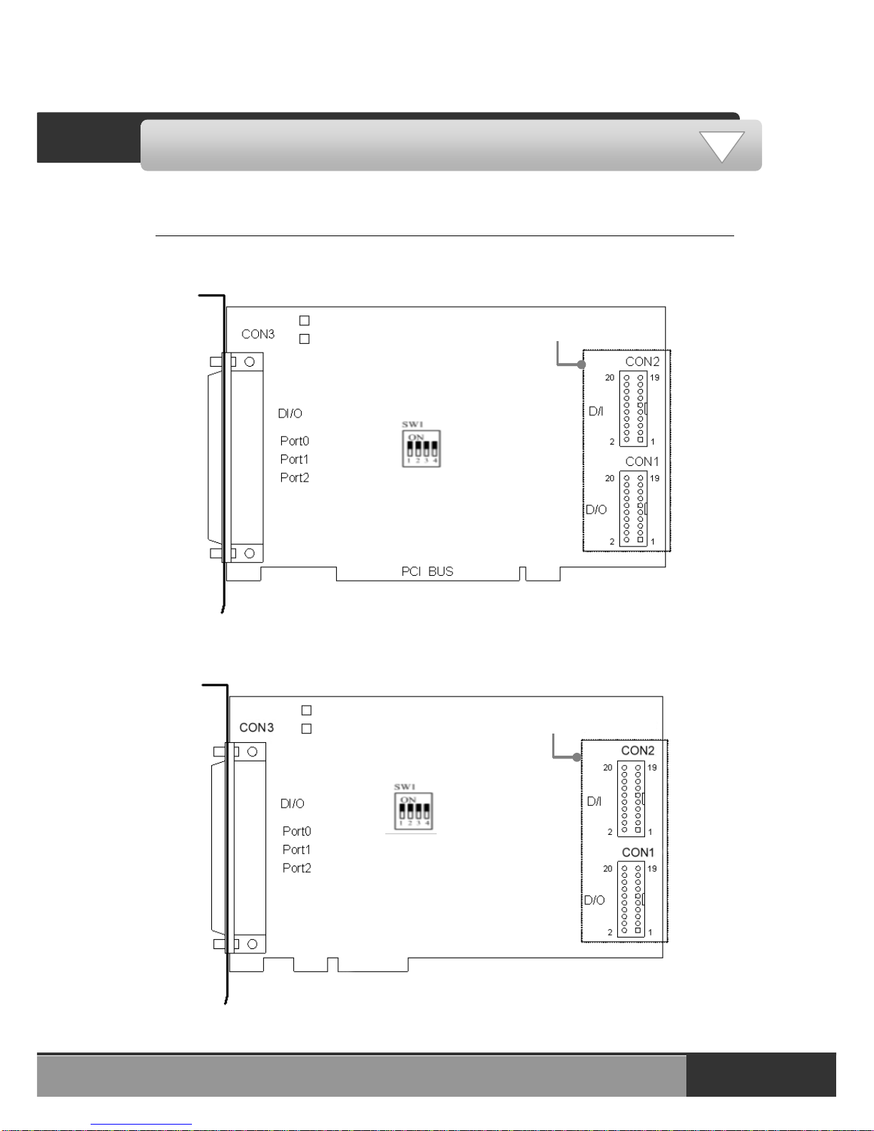
The board layout of the PIO-D24/D56 series cards are shown below:
The board layout of the PEX-D24/D56 cards are shown below:
Figure 2.1
Only for PIO-D24U/D56U
PIO-D56/D56U
PIO-D24/D24U
Only for PCI-D56/D56U
Figure 2.2
PCI Express Bus
Only for PEX-D56
PEX-D56
PEX-D24
Page 8
PIO/PEX-D24/D56 Series User Manual (Ver.3.1, Mar. 2015, PMH-005-31) 8
2.2 I/O Port Location
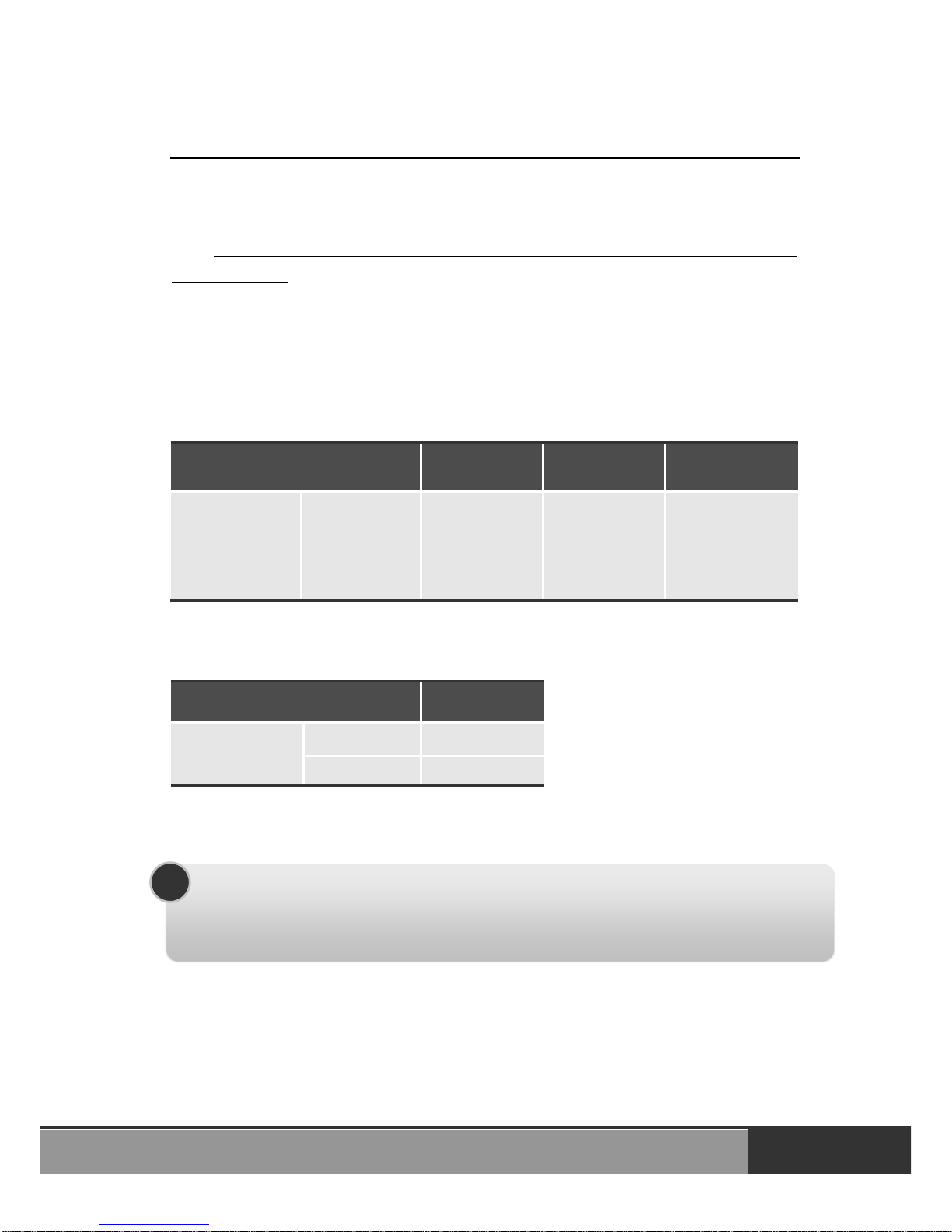
The PIO-D24/D56 series and PEX-D24/D56 consists of one 24-bit bi-directional
port, one 16-bit input port and one 16-bit output port (only for PIO-D56/D56U
and PEX-D56). The 24-bit port supports three 8-bit groups, which are PA, PB
and PC, respectively. Each 8-bit group can be configured as a D/I or D/O port
via the software. Note that when the PC is first turned on or if a reset has been
executed, all ports are set as D/I ports. Each I/O port is named as the following
table and its location can be found in Figure 2.1 and 2.2:
Table 2.1
Connector
PA0 ~ PA7
PB0 ~ PB7
PC0 ~ PC7
PIO-D24(U)
PIO-D56(U)
PEX-D24
PEX-D56
CON3
(D/I/O)
Port0
Port1
Port2
Refer to Sec. 2.1 for details of board layout and I/O port location.
Table 2.2
Connector
Description
PIO-D56(U)
PEX-D56
CON1
D/O
CON2
D/I
Refer to Sec. 2.1 for details of board layout and I/O port location.
Note:
P2C0, P2C1, P2C2, P2C3 interrupts and of the CON3 connector can be
used as an interrupt signal source. Refer to Sec. 2.5 for more
information.
!
Page 9
PIO/PEX-D24/D56 Series User Manual (Ver.3.1, Mar. 2015, PMH-005-31) 9
2.3 Card ID Switch
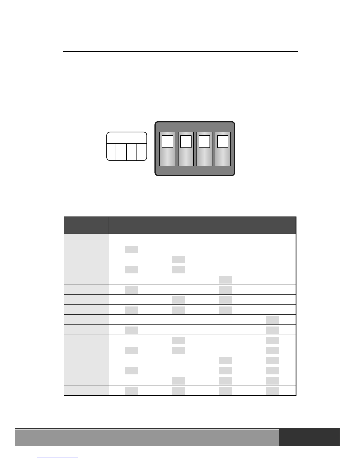
The PIO-D24U/D56U and PEX-D24/D56 has a Card ID switch with which users
can recognize the board by the ID via software when using two or more PIOD24U/ 56U and PEX-D24/D56 cards in one computer. The default Card ID is
0x0. For detail SW1 Card ID settings, please refer to Table 2.3.
Table 2.3 (*) Default Settings; OFF 1; ON 0
Card ID
(Hex)
1
ID0
2
ID1
3
ID2
4
ID3
(*) 0x0
ON
ON
ON
ON
0x1
OFF
ON
ON
ON
0x2
ON
OFF
ON
ON
0x3
OFF
OFF
ON
ON
0x4
ON
ON
OFF
ON
0x5
OFF
ON
OFF
ON
0x6
ON
OFF
OFF
ON
0x7
OFF
OFF
OFF
ON
0x8
ON
ON
ON
OFF
0x9
OFF
ON
ON
OFF
0xA
ON
OFF
ON
OFF
0xB
OFF
OFF
ON
OFF
0xC
ON
ON
OFF
OFF
0xD
OFF
ON
OFF
OFF
0xE
ON
OFF
OFF
OFF
0xF
OFF
OFF
OFF
OFF
NO
1 2 3 4
ID 0
ID 1
ID 2
ID 3
SW1
(Default Settings)
Page 10
PIO/PEX-D24/D56 Series User Manual (Ver.3.1, Mar. 2015, PMH-005-31) 10
P0A1
37
36
35
34
33
32
31
30
29
28
27
26
25
24
23
22
21
20
17
16
15
14
13
12
11
10 9 8
18
7
6 5 4 3 2
1
P0A2
N.C.
GND
Vcc
P0A0
P0A5
P0A6
P0A4
P0A3
N.C.
GND
P1B2
P1B0
P0A7
P2C0
P2C4
P2C3
P2C5
Vcc
P2C6
P2C1
P2C2
N.C.
P1B7
P2C7
N.C.
GND
P1B3
P1B4
P1B5
P1B6
19
GND
P1B1
GND
N.C.
GND
DI15
20
18
16
14
12
10
8
6
4
17
15
13
11
9
7
5
3
1
19
DI13
DI 14
GND
Vcc
GND
+12V
DI 7
DI 5
DI 9
DI11
DI 8
DI 6
DI 10
DI 12
DI 2
DI 4
DI 3
DI 0
2
DI 1
DO 15
20
18
16
14
12
10
8
6
4
17
15
13
11
9
7
5
3
1
19
DO 13
DO 14
GND
Vcc
GND
+12V
DO 7
DO 5
DO 9
DO 11
DO 8
DO 6
DO 10
DO 12
DO 2
DO 4
DO 3
DO 0
2
DO 1
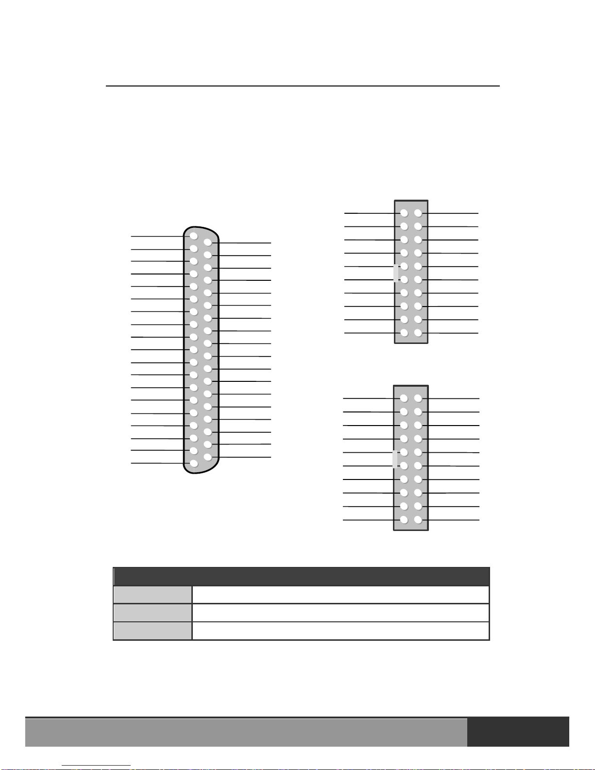
2.4 Pin Assignments
The Pin assignments for all PIO-D24/D56 series and PEX-D24/D56 connectors
are listed in Tables 2.3, 2.4 and 2.5. All signal sources for each digital input or
output pin (channel) are TTL compatible.
CON3: 37-Pin D-type female connector
CON2: 20-Pin of box header
CON1: 20-Pin of box header
All Signals are TTL Compatible
High (1)
2.0 ~ 5.0 V(Voltage over 5.0V will damage the device)
None Define
2.0 V ~ 0.8 V
Low(0)
Under 0.8 V
Page 11
PIO/PEX-D24/D56 Series User Manual (Ver.3.1, Mar. 2015, PMH-005-31) 11
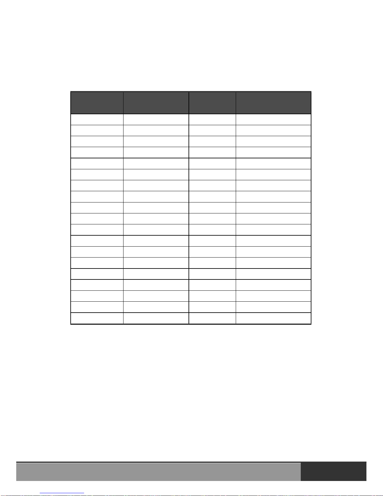
Table 2.4 37-Pin D-type female connector for Port0~Port2
PIO-D24(U)/D56(U) and PEX-D24/D56: CON3 Connector
Pin
Number
Description
Pin
Number
Description
1
N. C.
20
VCC
2
N. C.
21
GND
3
P1B7
22
P2C7
4
P1B6
23
P2C6
5
P1B5
24
P2C5
6
P1B4
25
P2C4
7
P1B3
26
P2C3
8
P1B2
27
P2C2
9
P1B1
28
P2C1
10
P1B0
29
P2C0
11
GND
30
P0A7
12
N.C.
31
P0A6
13
GND
32
P0A5
14
N.C.
33
P0A4
15
GND
34
P0A3
16
N.C.
35
P0A2
17
GND
36
P0A1
18
VCC
37
P0A0
19
GND
XXXXXXX
This pin not available
Page 12
PIO/PEX-D24/D56 Series User Manual (Ver.3.1, Mar. 2015, PMH-005-31) 12
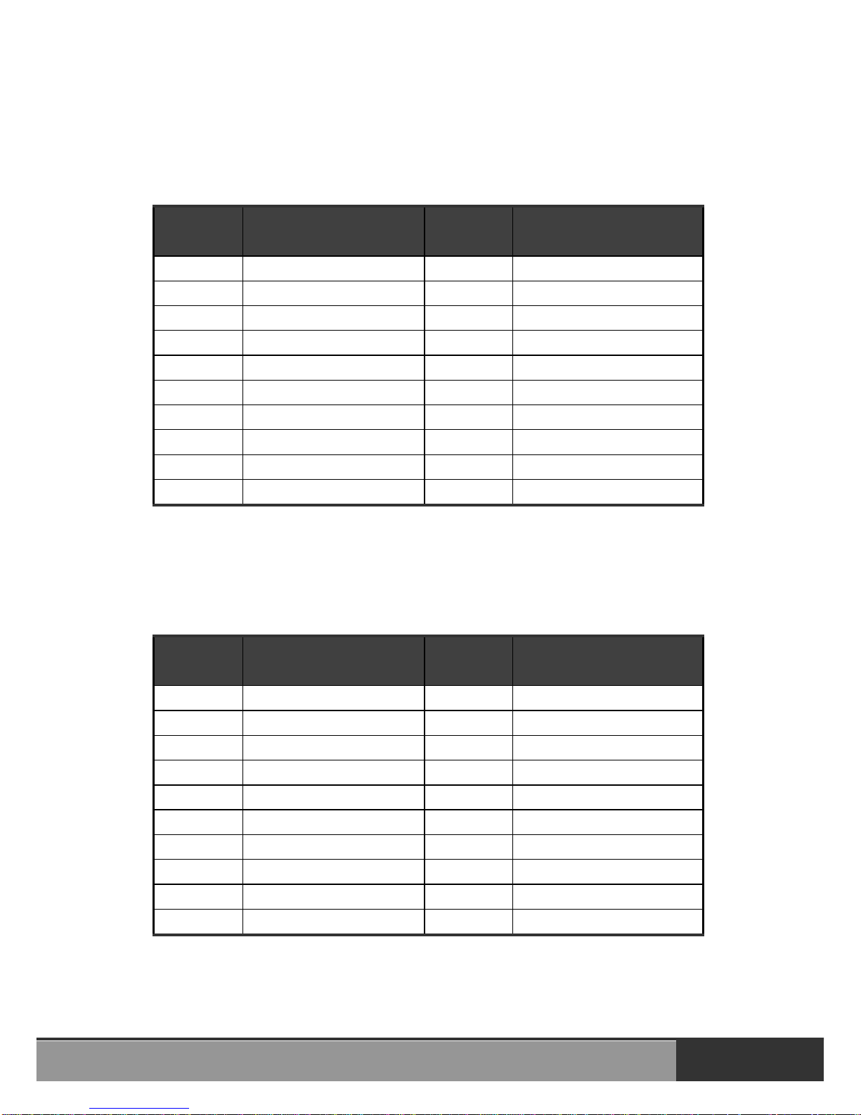
Table 2.5 20-Pin flat-cable headers of D/I for PIO-D56(U) and PEX-D56
PIO-D56(U) and PEX-D56: CON2 Connector
Pin
Number
Description
Pin
Number
Description
1
DI0 2 DI1
3
DI2 4 DI3
5
DI4 6 DI5
7
DI6 8 DI7
9
DI8
10
DI9
11
DI10
12
DI11
13
DI12
14
DI13
15
DI14
16
DI15
17
GND
18
GND
19
Vcc
20
+12 V
Table 2.6 20-Pin flat-cable headers of D/O for PIO-D56(U) and PEX-D56
PIO-D56(U) and PEX-D56: CON1 Connector
Pin
Number
Description
Pin
Number
Description
1
DO0
2
DO1
3
DO2
4
DO3
5
DO4
6
DO5
7
DO6
8
DO7
9
DO8
10
DO9
11
DO10
12
DO11
13
DO12
14
DO13
15
DO14
16
DO15
17
GND
18
GND
19
Vcc
20
+12 V
Page 13
PIO/PEX-D24/D56 Series User Manual (Ver.3.1, Mar. 2015, PMH-005-31) 13
2.5 Enable I/O Operation
When the PC is first powered-on, the operations of all digital I/O channels for
each port are disabled. Note that the digital I/O channel for each port is enabled
or disabled using the RESET\ signal. Refer to Sec. 3.3.1 for more information.
The power-on states for all DI/O ports are as follows:
D/I/O operations for each port are disabled.
D/I/O ports are all configured as Digital input ports.
D/O latch registers are all undefined. Refer to Sec. 2.5 for details.
The user must perform an initialization procedure before using these digital I/O
ports. The recommended steps are as follows:
Step 1: Determine the address mapping of the PIO/PISO cards.
(Refer to Sec.3.1 for details)
Step 2: Enable all Digital I/O operations. (Refer to Sec. 3.3.1 for details)
Step 3: Select the controlled port for 37-Pin D-type female connector (CON3) to
their expected D/I/O states and send their initial values to every D/O
port. (Refer to Sec. 3.3.7 and 3.3.9 for details)
For more information regarding the initialization procedure for digital I/O
ports, please refer to the DEMO1.C demo program.
Page 14
PIO/PEX-D24/D56 Series User Manual (Ver.3.1, Mar. 2015, PMH-005-31) 14
2.5.1 D/I/O Port Architecture
Connector
Description
PIO-D24/D56 series
PEX-D24/D56
CON3
Programmable Digital I/O
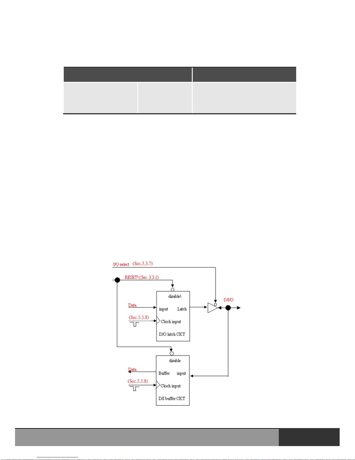
The programmable digital I/O control architecture for the PIO-D24/D56 series
and PEX-D24/D56 is illustrated in Figure 2.2. The operation method of control
signal is described below.
When the RESET\ signal is in the Low-state, if means that all D/I/O
operations are disabled.
When RESET\ signal is in the High-state, if means all D/I/O operations are
enabled.
If the D/I/O is configured as a D/I port, the port can accept D/I from external
signal sources
If the D/I/O is configured as a D/O port, the D/O value can be read from the
port.
If D/I/O is configured as a D/I port, sending data to the Digital input port will
only change the D/O latch register. The latched data will be output when the
port is configured as digital output and is activated right away.
Figure 2.2
Page 15
PIO/PEX-D24/D56 Series User Manual (Ver.3.1, Mar. 2015, PMH-005-31) 15
2.5.2 D/I Port Architecture
Connector
Description
PIO-D56/D56U
PEX-D56
CON2
Digital Input
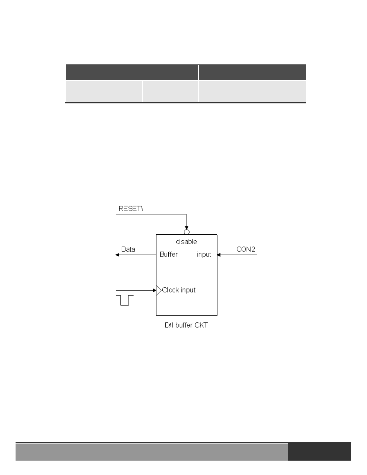
The digital input control architecture for the PIO-D56/D56U and PEX-D56 is
demonstrated in Figure 2.3.
When the RESET\ signal is in the Low-state, if means that all D/I operations
are disabled.
When RESET\ signal is in the High-state, if means all D/I operations are
enabled.
Figure2.3 D/I Port Architecture
Page 16
PIO/PEX-D24/D56 Series User Manual (Ver.3.1, Mar. 2015, PMH-005-31) 16
2.5.3 D/O Port Architecture
Connector
Description
PIO-D56/D56U
PEX-D56
CON1
Digital Output
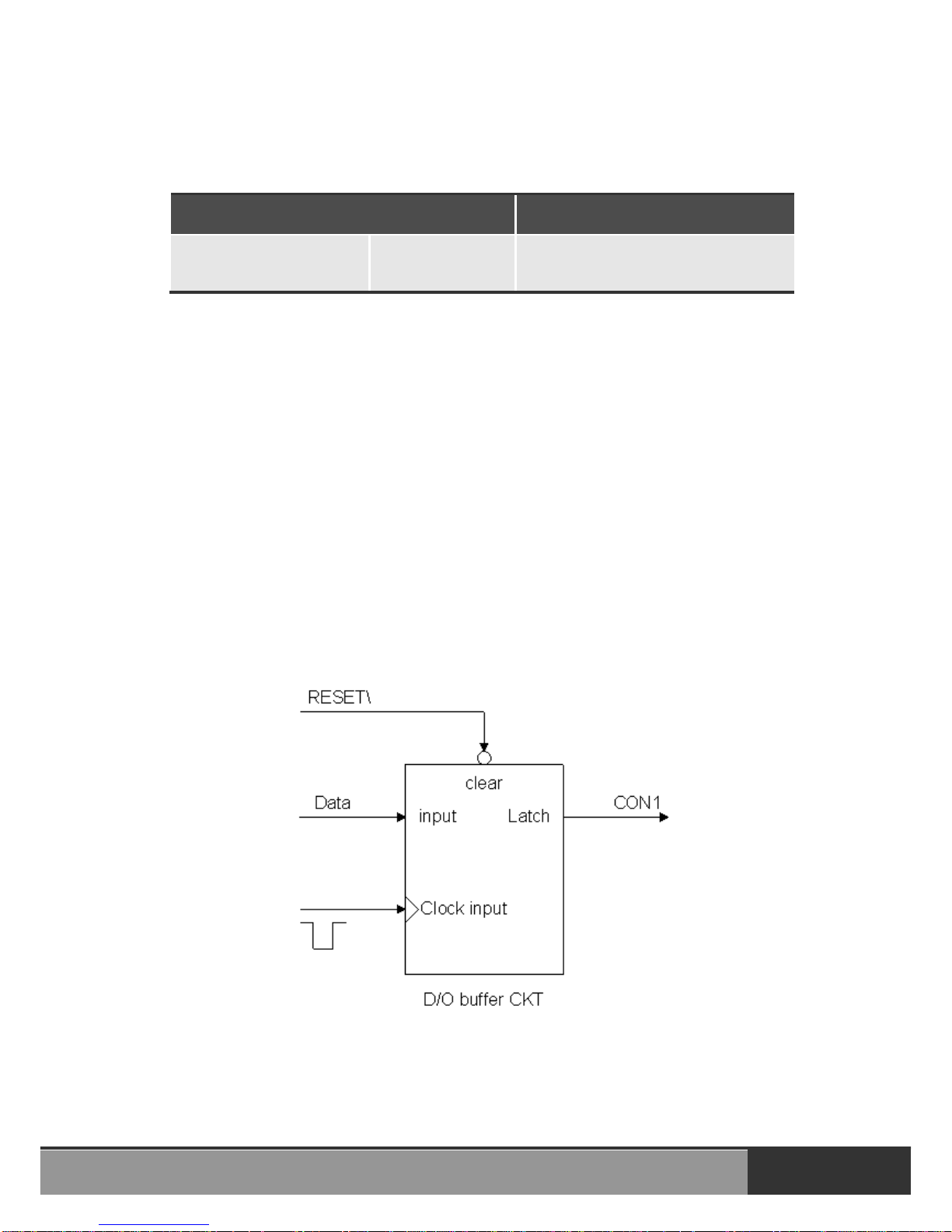
The digital output control architecture for the PIO-D56/D56U and PEX-D56 is
demonstrated in Figure 2.4.
When the RESET\ signal is in the Low-state, if means that all D/O
operations are disabled.
When RESET\ signal is in the High-state, if means all D/O operations are
enabled.
The power-on states are as follows:
All DO operations are disabled
All output latches are cleared to Low-Level
Figure2.4 D/O Port Architecture
Page 17
PIO/PEX-D24/D56 Series User Manual (Ver.3.1, Mar. 2015, PMH-005-31) 17
2.6 Interrupt Operation
The P2C0, P2C1, P2C2 and P2C3 interrupts pins of the 37-Pin D-type female
connector (CON3) can be used as an interrupt signal source. Refer to Sec. 2.1
for the P2C0/P2C1/P2C2/P2C3 location. The interrupt of the PIO-D24/D56
series and PEX-D24/D56 is level-triggered and is Active_High. The interrupt
signal can be programmed as either inverted or non-inverted. The procedures
for how to configure the interrupt signal source are given as follows:
1. Determine whether the initial level is either High or Low from the signal
source.
2. If the initial state is High, select the inverted setting for the interrupt signal
source (Section. 3.3.6). If the initial state is Low, select the non-inverted
setting for the interrupt signal source (Section. 3.3.8)
3. Enable the interrupt function (Section. 3.3.4)
4. If the interrupt signal is active, the interrupt service routine will be
automatically started.
Note that DEMO3.C and DEMO4.C are demo programs for a single interrupt
source and DEMO5.C is a demo program for four interrupt sources in a DOS
operating system. If only one interrupt signal source is used, the interrupt
service routine does not need to identify the interrupt source. (Refer to
DEMO3.C and DEMO4.C). However, if there is more than one interrupts source,
the interrupt service routine needs to identify the active signals as follows:
(Refer to DEMO5.C)
Page 18
PIO/PEX-D24/D56 Series User Manual (Ver.3.1, Mar. 2015, PMH-005-31) 18
1. Read the new status of the interrupt signal source
2. Compare the new status with the old status to identify the active signals
3. If P2C0 is active, service P2C0 and non-inverter/inverted as the P2C0
signal
4. If P2C1 is active, service P2C1 and non-inverted/inverted as the P2C1
signal
5. If P2C2 is active, service P2C2 and non-inverted/inverted as the P2C2
signal
6. If P2C3 is active, service P2C3 and non-inverted/inverted the P2C3
signal
7. Save the new status to old status
Limitation: if the interrupt signal is too short, the new status may be the same as
the old status. In this case, the interrupt signal must be held at active until the
interrupt service routine is executed. This hold time is different for different OS
versions and can be as short as micro-second or as a long as second. In
general, 20 ms is enough for all types of OS.
Page 19
PIO/PEX-D24/D56 Series User Manual (Ver.3.1, Mar. 2015, PMH-005-31) 19
2.7 Daughter Boards
2.7.1 DB-37
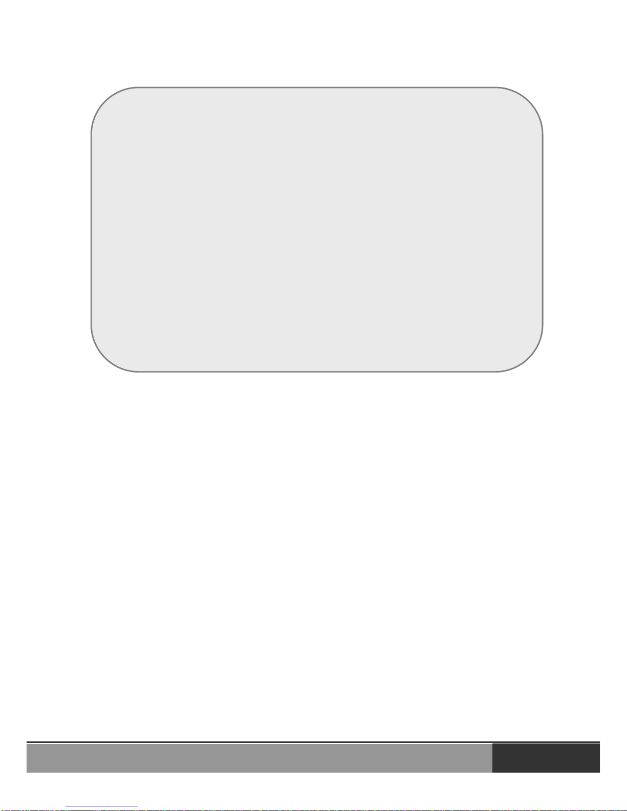
The DB-37 is a general-purpose daughter board for D-sub 37-pin devices, and
is designed for easy wiring.
Figure 2.5
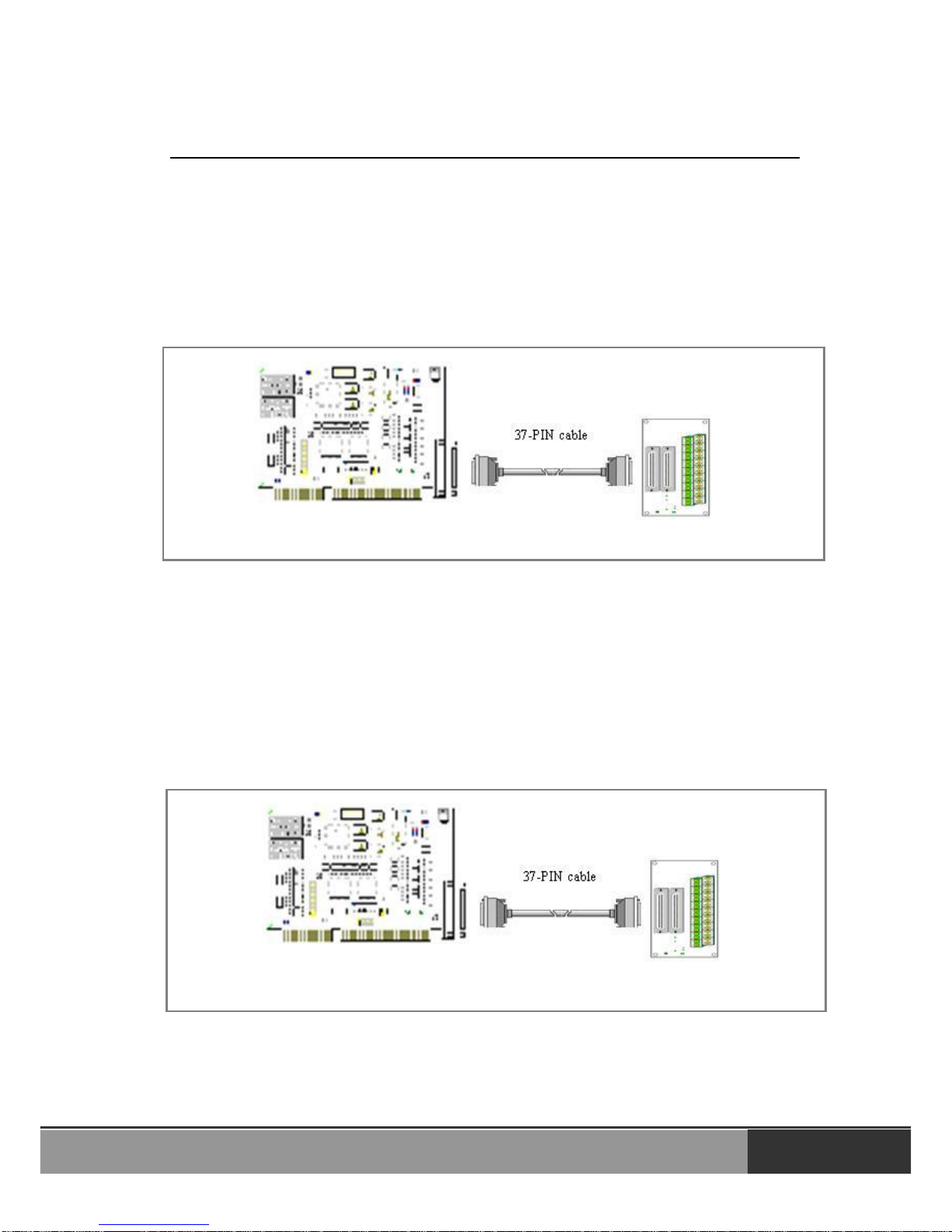
2.7.2 DN-37 and DN-50
The DN-37 is a general-purpose daughter board for the DB-37 using DIN-Rail
Mounting. The DN-50 is designed for a 50-pin flat-cable header using DIN-Rail
mounting. They are also designed for easy wiring.
Figure 2.6
Page 20
PIO/PEX-D24/D56 Series User Manual (Ver.3.1, Mar. 2015, PMH-005-31) 20
2.7.3 DB-8125
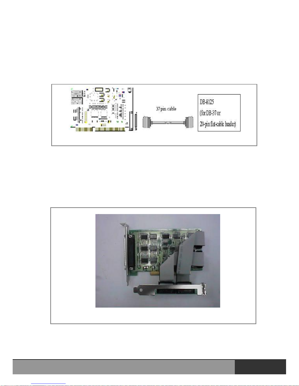
The DB-8125 is a general-purpose screw terminal board and is designed for easy
wiring. The DB-8125 uses a single DB-37 header and two 20-pin flat-cable
headers.
Figure 2.7
2.7.4 ADP-20/PCI
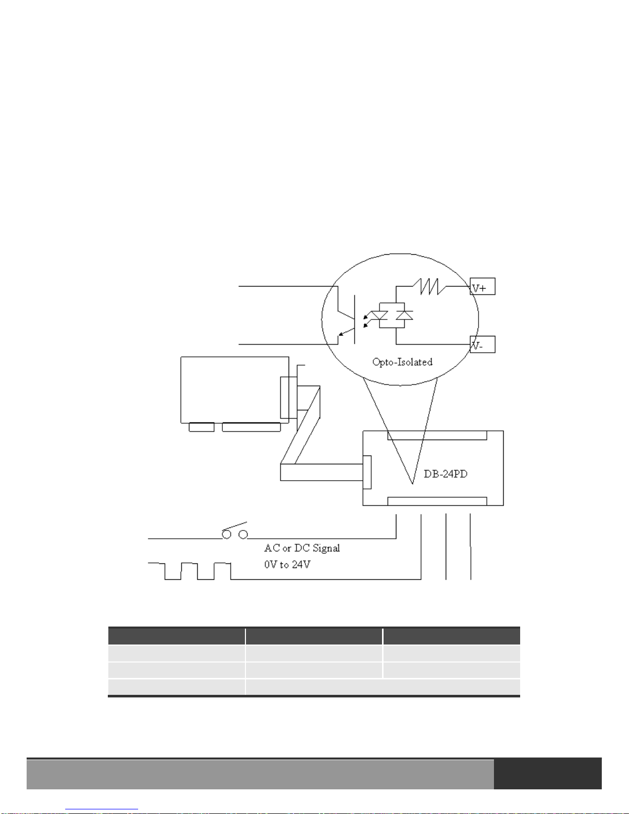
The ADP-20/PCI is an extender for the 20-pin header. The one side of the ADP20/PCI can be connected to a 20-pin header. The other side can be mounted
onto the PC chassis as is depicted by the following:
Figure 2.8
Page 21
PIO/PEX-D24/D56 Series User Manual (Ver.3.1, Mar. 2015, PMH-005-31) 21
2.7.5 DB-24P, DB-24PD Isolated Input Board
The DB-24P is a 24-channel isolated digital input daughter board. The optically
isolated inputs of the DB-24P consist of a bi-directional optocoupler with a
resistor for current sensing. The DB-24P can be used to sense DC signals from
TTL levels up to 24 V, or use the DB-24P to sense a wide range of AC signals.
This board can also be used to isolate the computer from large common-mode
voltage, ground loops and transient voltage spikes that often occur in industrial
environments, as shown in Figure 2.9. Table 2.6 is comparison of the DB-24P
and DB-24PD.
Figure 2.9
Table 2.7
DB-24P
DB-24PD
50-pin flat-cable header
Yes
Yes
D-sub 37-pin header
No
Yes
Other specifications
Same
PIO-D24/D56 series
PEX-D24/D56
PIO-D24/D56 series
PEX-D24/D56
Page 22
PIO/PEX-D24/D56 Series User Manual (Ver.3.1, Mar. 2015, PMH-005-31) 22
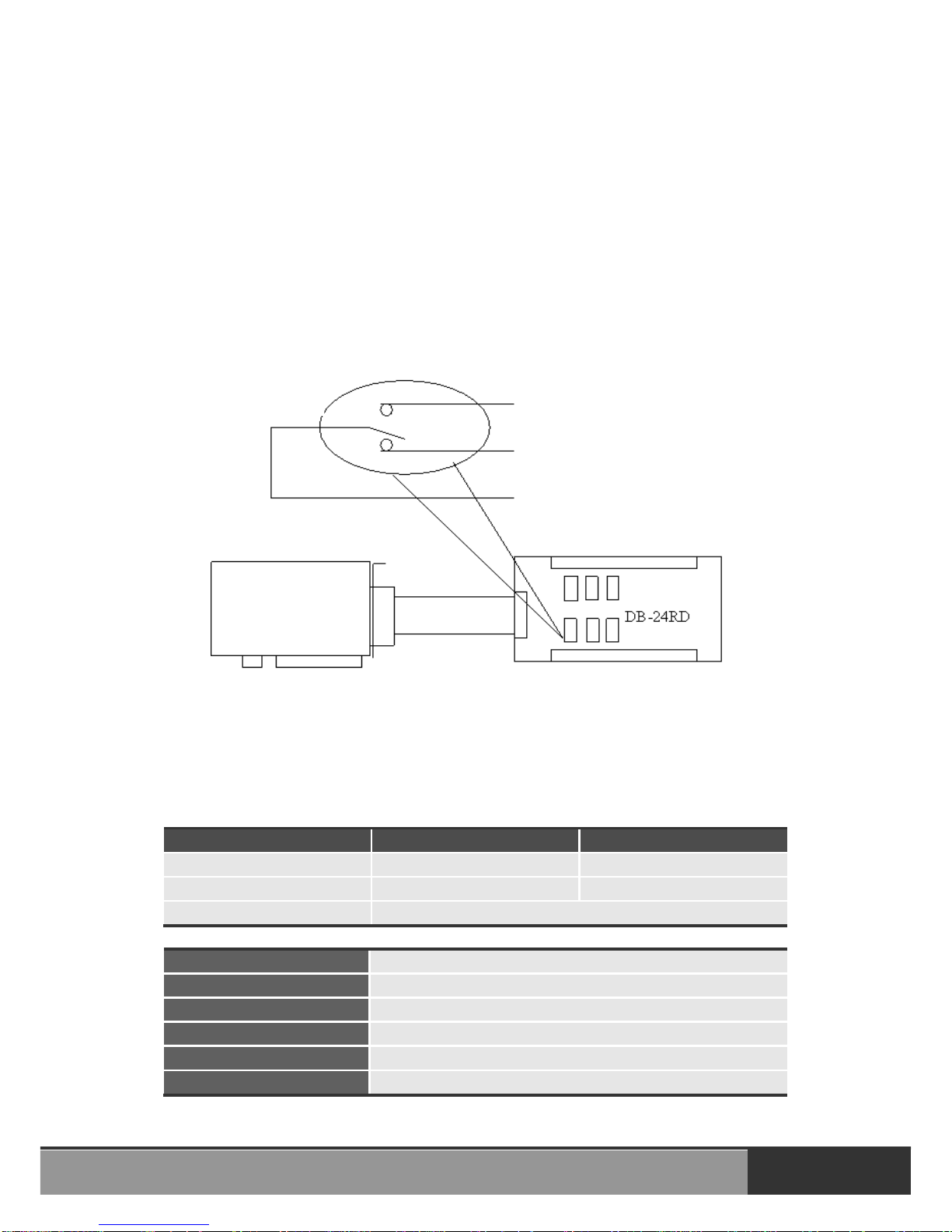
2.7.6 DB-24R, DB-24RD Relay Board
The DB-24R is a 24-channel relay output board consisting of 24 Form-C relays
for efficient programmable control of the load switching. The relays are powered
by applying a 12 V/24 V voltage signal to the appropriate relay channel on the
50-pin flat-cable connector. There are 24 enunciator LEDs for each relay
channel and the LED is light when their associated relay is activated. The
control scheme is illustrated in Figure 2.10 below. Table 2.7 gives a comparison
and Table 2.8 gives a description of the daughter boards used in this application.
Table 2.8
DB-24R
DB-24RD
50-pin flat-cable header
Yes
Yes
D-sub 37-pin header
No
Yes
Other specifications
Same
Table 2.9
DB-24R, DB-24RD
24 × Relay (120 V, 0.5 A)
DB-24PR,DB-24PRD
24 × Power Relay (250 V, 5 A)
DB-24POR
24 × Photo MOS Relay (350 V, 01 A)
DB-24SSR
24 × SSR (250 VAC, 4 A)
DB-24C
24 × O.C. (30 V, 100 mA)
DB-16P8R
16 × Relay (120 V, 0.5 A) + 8 × isolated input
PIO-D24/D56 series
PEX-D24/D56
Notes: Channels: 24 Form C Relay
Relays: Switching of up to 0.5 A at
110 VAC or 1 A at 24 VDC
Normally Open
Normally Closed
Form C Relay
Com
Figure 2.8
Page 23
PIO/PEX-D24/D56 Series User Manual (Ver.3.1, Mar. 2015, PMH-005-31) 23
2.7.7 DB-24PR, DB-24POR, DB-24C
Table 2.10
DB-24PR
24 × Power relay, 5 A/250 V
DB-24POR
24 × Photo MOS relay, 0.1 A/350 VAC
DB-24C
24 × Open Collector, 100 mA per channel, 30 V max.
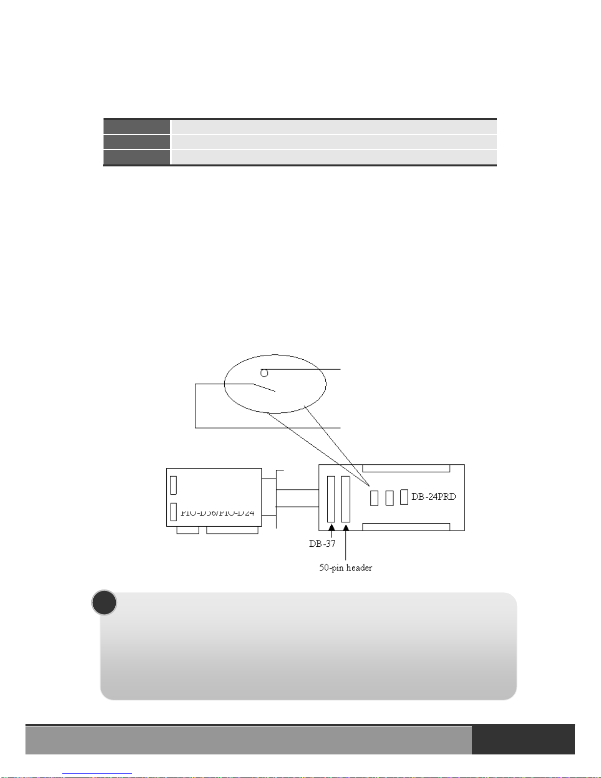
The DB-24PR is a 24-channel power relay output board consisting of 8 Form-C
and 16 Form-A electromechanical relays for efficient programmable control of
the load switching. The contact of each relay can allow a 5 A current load at 250
VAC/30 VDC. The relay is powered by applying a 5 voltage signal to the
associated relay channel on the 20-pin flat-cable connector (only uses 16 relays)
or 50-pin flat-cable connector (OPTO-22 compatible, for DIO-24 series). 24
enunciator LEDs for indicating the status of for each relay and the corresponding
LED is light when their associated relay is activated. To avoid overloading your
PC’s power supply, this board needs a +12 VDC or +24 VDC external power
supply, as shown in Figure 2.11.
Notes:
1. A 50-Pin connector (OPTO-22 compatible) is used, for DIO-24/48/
144, PIO-D144, PIO-D96, PIO-D56, PIO-D48, PIO-D24, PIO-D168
2. A 20-Pin connector for 16-channel digital output is used for A-82X,
A-62X, DIO-64, ISO-DA16/DA8,
3. Channels: 16 Form A Relay, 8 Form C Relay.
4. Relays: Switching of up to 5 A at 110 VAC/5 A at 30 VDC.
!
Normally Open
Form A Relay
COM
Figure 2.11
PIO-D24/D56 series
PEX-D24/D56
Page 24
PIO/PEX-D24/D56 Series User Manual (Ver.3.1, Mar. 2015, PMH-005-31) 24
2.7.8 Daughter Board Comparison Table
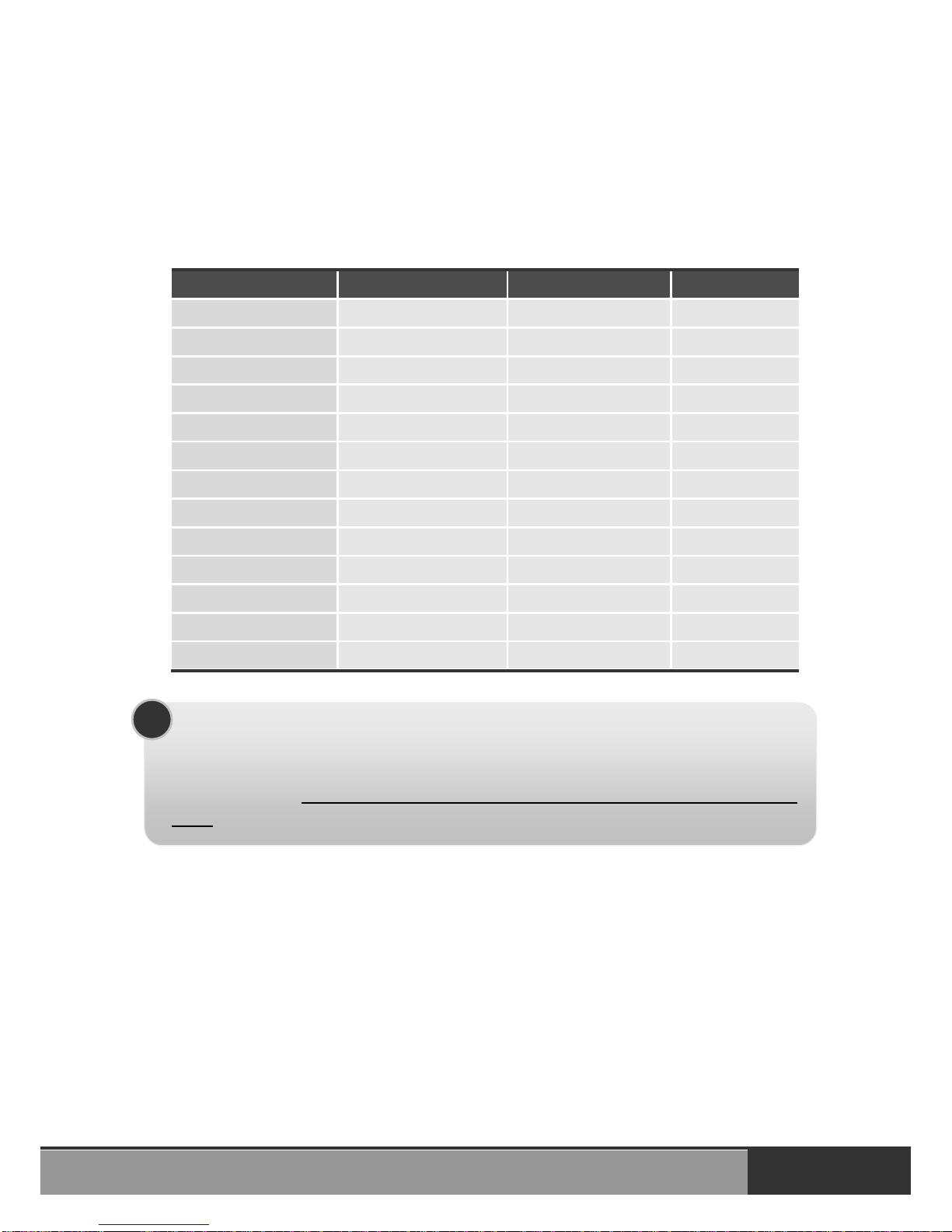
Table 2.10 lists a comparison for the daughter board applications using
PIO/PISO series cards.
Table 2.11
20-pin flat-cable
50-pin flat-cable
D-sub 37-pin
DB-37
No
No
Yes
DN-37
No
No
Yes
ADP-37/PCI
No
Yes
Yes
ADP-50/PCI
No
Yes
No
DB-24P
No
Yes
No
DB-24PD
No
Yes
Yes
DB-16P8R
No
Yes
Yes
DB-24R
No
Yes
No
DB-24RD
No
Yes
Yes
DB-24C
Yes
Yes
Yes
DB-24PRD
No
Yes
Yes
DB-24POR
Yes
Yes
Yes
DB-24SSR
No
Yes
Yes
Note:
There is no 50-pin flat cable header in the PIO-D24/D56 series and PEX-
D56/D24. The PIO-D24/D56 series and PEX-D56/D24 has one DB-37
connector and two 20 pin flat-cable headers (only for PIO-D56(U)/PEX-
D56).
!
Page 25
PIO/PEX-D24/D56 Series User Manual (Ver.3.1, Mar. 2015, PMH-005-31) 25
3. I/O Control Register
3.1 How to Find the I/O Address
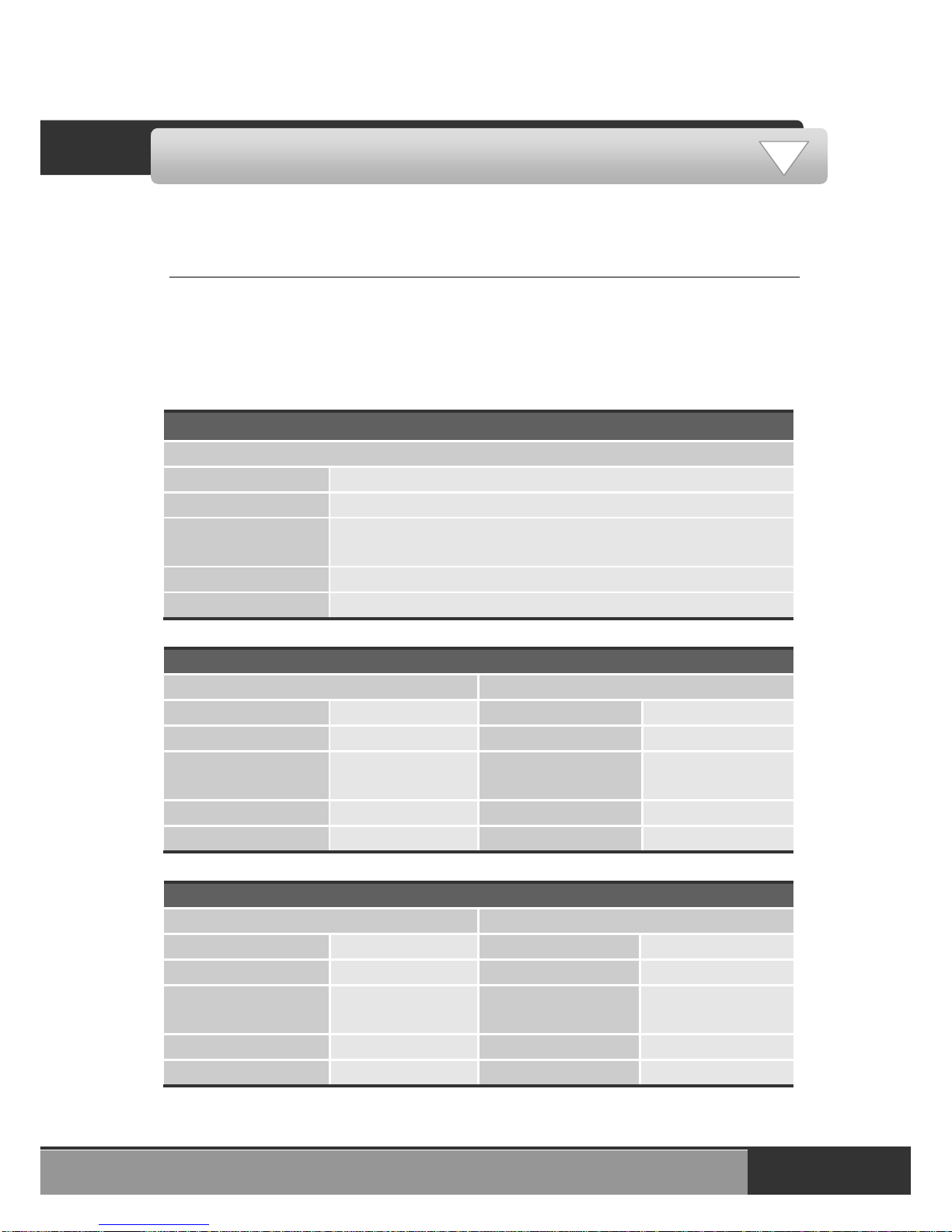
The Plug & Play BIOS will assign an appropriate I/O address to each PIO/PISO
series card during the power-on stage. The fixed IDs of the PIO-D24/D56
series and PEX-D24/D56 cards are as following:
For PIO-D24U/D56U and PEX-D24/D56
Rev 1.0 or above
Vendor ID
0xE159
Device ID
0x0001
Sub-vendor ID
0x8080
0xC080
Sub-device ID
0x01
Sub-aux ID
0x40
For PIO-D24
Rev 1.0~Rev 5.0
Rev 6.0 or above
Vendor ID
0xE159
Vendor ID
0xE159
Device ID
0x0002
Device ID
0x0001
Sub-vendor ID
0x80
Sub-vendor ID
0x8080
0xC080
Sub-device ID
0x01
Sub-device ID
0x01
Sub-aux ID
0x40
Sub-aux ID
0x40
For PIO-D56
<Rev 1.0 ~ Rev 4.0>
Rev 5.0 or above
Vendor ID
0xE159
Vendor ID
0xE159
Device ID
0x0002
Device ID
0x0001
Sub-vendor ID
0x80
Sub-vendor ID
0x8080
0xC080
Sub-device ID
0x01
Sub-device ID
0x01
Sub-aux ID
0x40
Sub-aux ID
0x40
Page 26
PIO/PEX-D24/D56 Series User Manual (Ver.3.1, Mar. 2015, PMH-005-31) 26
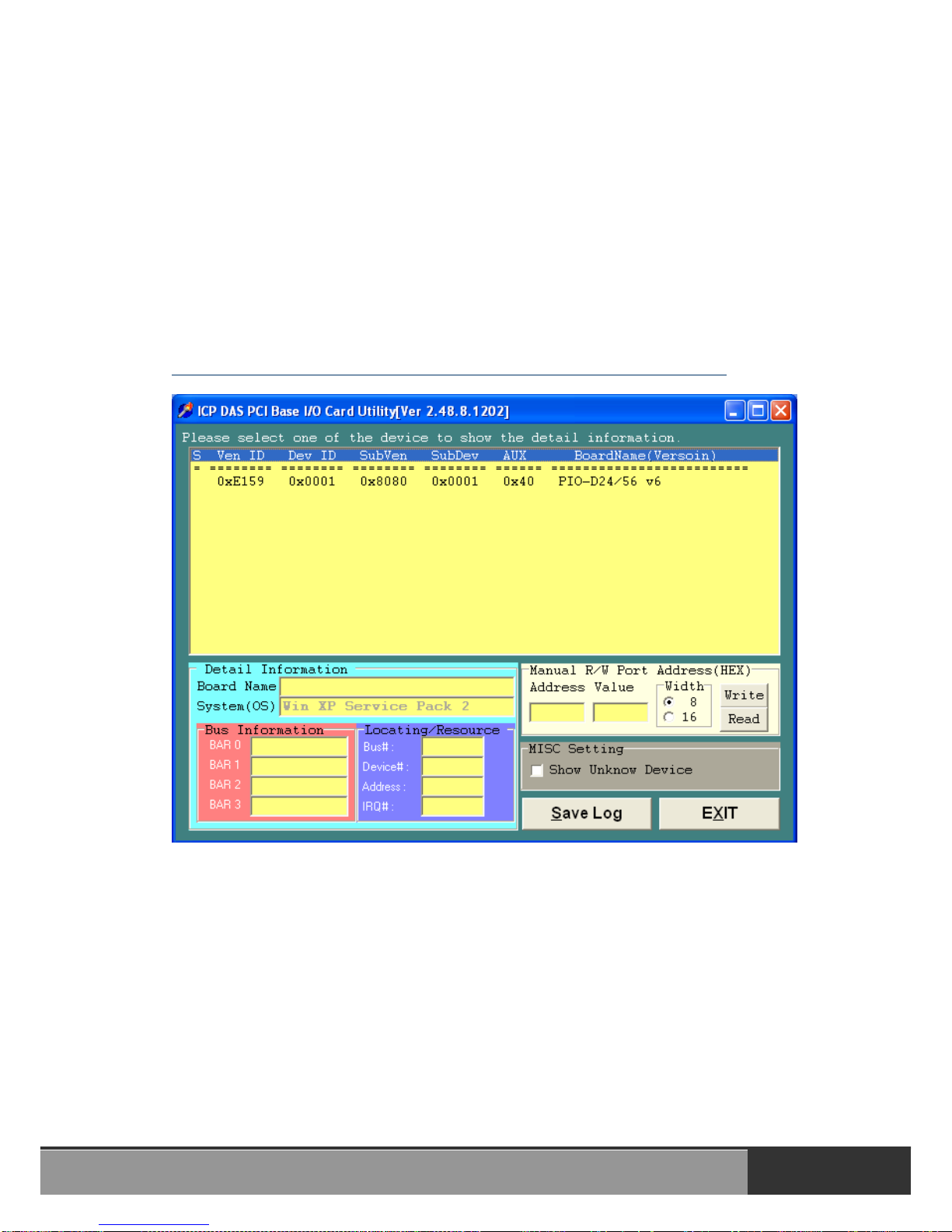
The PIO_PISO.EXE utility program will detect and present all information for
PIO/PISO cards installed in the PC, as shown in the following figure3.1.
Details of how to identify the PIO series cards of ICPDAS data acquisition
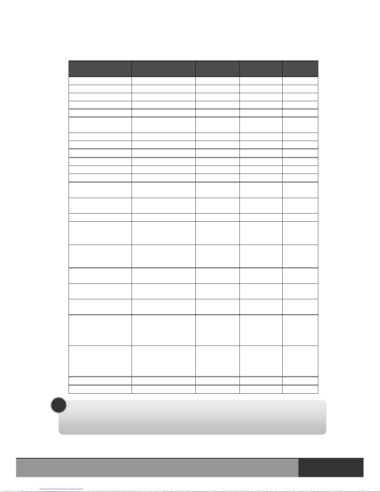
boards based on the Sub-vendor, Sub-device and Sub-Aux ID are given in
Table 3-1.
The PIO_PISO.exe utility is located on the CD as below and is useful for all
PIO/PISO series cards.
CD:\NAPDOS\PCI\Utility\Win32\PIO_PISO\
http://ftp.icpdas.com/pub/cd/iocard/pci/napdos/pci/utility/win32/pio_piso/
Figure 3.1
Page 27
PIO/PEX-D24/D56 Series User Manual (Ver.3.1, Mar. 2015, PMH-005-31) 27
Table 3-1
PIO/PISO series
card
Description
Sub_Vendor
Sub_Device
Sub_AUX
PIO-D168
168 * DIO
9880
01
50
PIO-D168A
168 * DIO
80
01
50
PIO-D144(REV4.0)
144 * D/I/O
80 (5C80)
01
00
PIO-D96 (REV4.0)
96 * D/I/O
80 (5880)
01
10
PIO-D64 (REV2.0)
64 * D/I/O
80 (4080)
01
20
PIO-D56 (REV5.0)
24 * D/I/O +
16 * D/I+16*D/O
80 (8080)
01
40
PIO-D48 (REV2.0)
48 * D/I/O
80 (0080)
01
30
PIO-D24 (REV6.0)
24 * D/I/O
80 (8080)
01
40
PIO-821
Multi-function
80
03
10
PIO-DA16
16 * D/A
80
04
00
PIO-DA8
8 * D/A
80
04
00
PIO-DA4
4 * D/A
80
04
00
PISO-C64
64 * isolated D/O
(Current sinking)
80
08
00
PISO-A64
64 * isolated D/O
(Current sourcing)
80
08
50
PISO-P64
64 * isolated D/I
80
08
10
PISO-P32C32
32* isolated D/O
(Current sinking)
+ 32* isolated D/I
80
08
20
PISO-P32A32
32*isolated DO
(Current sourcing)
+ 32* isolated D/I
80
08
70
PISO-P8R8
8* isolated D/I +
8 * 220 V relay
80
08
30
PISO-P8SSR8AC
8* isolated D/I +
8 * SSR /AC
80
08
30
PISO-P8SSR8DC
8* isolated D/I +
8 * SSR /DC
80
08
30
PISO-730
16*DI + 16*D/O +
16* isolated D/I +
16*isolated D/O
(Current sinking)
80
08
40
PISO-730A
16*DI + 16*D/O +
16* isolated D/I +
16*isolated D/O
(Current sourcing)
80
08
80
PISO-813
32 * isolated A/D
80
0A
00
PISO-DA2
2 * isolated D/A
80
0B
00
Note:
If your board is a different version, it may also have different Sub IDs.
However this will present no actual problem. No matter which version of
the board you select, we offer the same function calls.
!
Page 28
PIO/PEX-D24/D56 Series User Manual (Ver.3.1, Mar. 2015, PMH-005-31) 28
3.2 The Assignment of I/O Addresses
The Plug & Play BIOS will assign an appropriate I/O address to the PIO/PISO
series card. If there is only one PIO/PISO board, the board will be identified as
card_0. If there are two PIO/PISO boards in the system, it is very difficult to
identify which board is card_0. The software driver can support a maximum of
16 boards. Therefore, the user can install 16 PIO/PSIO series cards in one PC
system. Details of how to locate and identify card_0 and card_1 are provided
below:
The simplest way to identify which card is card_0 is to use the wSlotBus
and wSlotDevice functions as follows:
Step 1: Remove all PIO-D24/D56 or PEX-D24/D56 series cards from the PC.
Step 2: Install a single PIO-D24/D56 or PEX-D24/D56 series card into the
PCI_slot1 in the PC, then run PIO_PISO.EXE and record the
wSlotBus1 and wSlotDevice1 information.
Step 3: Remove all PIO-D24/D56 or PEX-D24/D56 series cards from the PC.
Step 4: Install a single PIO-D24/D56 or PEX-D24/D56 series cards into the
PCI_slot2 in the PC, then run PIO_PISO.EXE and record the
wSlotBus2 and wSlotDevice2 information.
Step 5: Repeat Steps 3 and 4 for all PCI_slots and record all wSlotBus and
wSlotDevice information.
Page 29
PIO/PEX-D24/D56 Series User Manual (Ver.3.1, Mar. 2015, PMH-005-31) 29
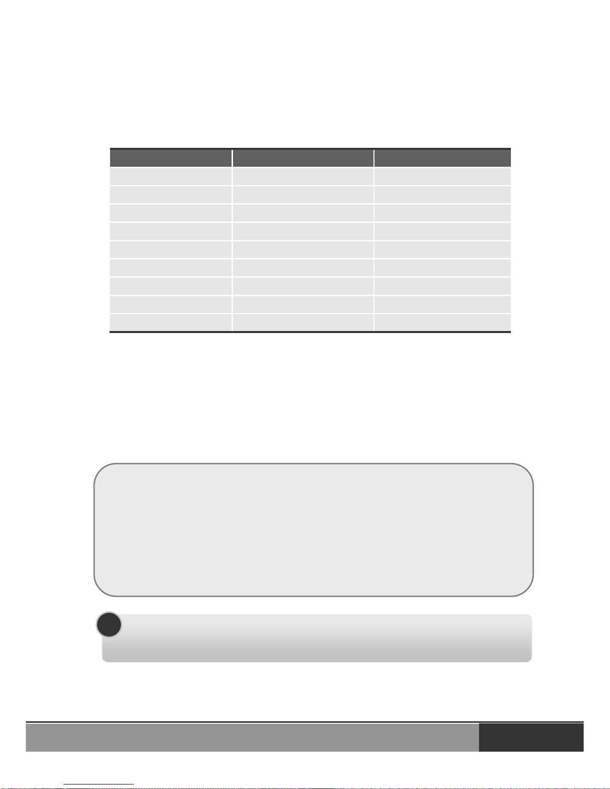
The records may be similar to the following table:
Table 3-2
PC’s PCI slot
wSlotBus
wSlotDevice
Slot_1
0
0x07
Slot_2
0
0x08
Slot_3
0
0x09
Slot_4
0
0x0A
PCI-BRIDGE
Slot_5
1
0x0A
Slot_6
1
0x08
Slot_7
1
0x09
Slot_8
1
0x07
The above procedure is used to record all the wSlotBus and wSlotDevice
information for the PC. These values will be mapped to this PC’s physical slots
and this mapping will not be changed for any PIO/PISO cards. Therefore, this
information can be used to identify the specific PIO/PISO card using the
following steps:
Step 1: Using the wSlotBus and wSlotDevice information from Table 3-2, enter
the board number into the PIO_GetConfigAddressSpace(…) function
to get the information for a specific card information, especially
wSlotBus and wSlotDevice details.
Step 2: Identify the specific PIO/PISO card by comparing the data of the
wSlotBus and wSlotDevice from Step 1.
Note that, normally, the card that is installed in slot 0 is card0 and the
card installed in slot1 is card1 for PIO/PISO series cards.
!
Page 30
PIO/PEX-D24/D56 Series User Manual (Ver.3.1, Mar. 2015, PMH-005-31) 30
3.3 The I/O Address Map
The I/O address of the PIO/PISO series card is automatically assigned by
the main board ROM BIOS. The I/O address can also be re-assigned by the
user, but It is strongly recommended that the I/O address is not changed by
user. The Plug & Play BIOS will assign an appropriate I/O address to each
PIO/PISO series card. The I/O addresses of the PIO-D24/D56 and PEX-
D24/D56 series cards are as follows, and are based on the base address of
each card.
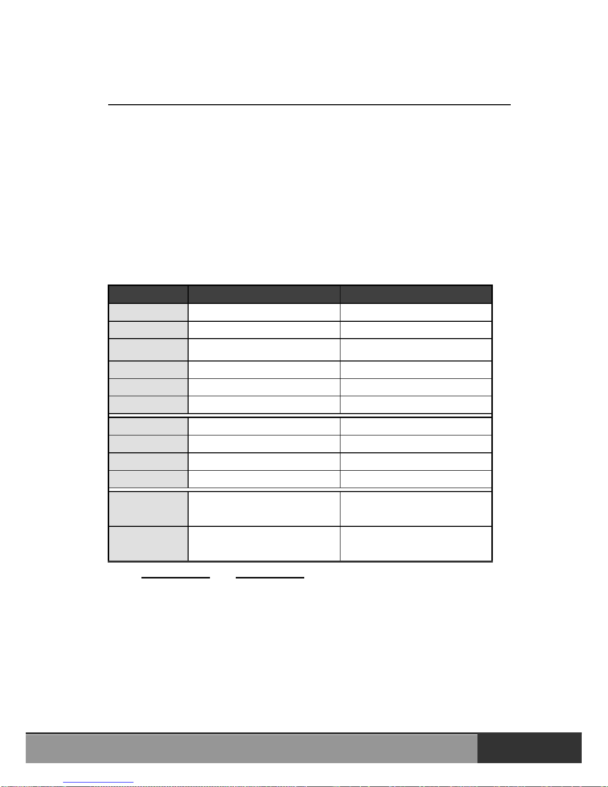
Table 3-3
Address
Read
Write
Wbase+0
Reserved
RESET\ control register
Wbase+2
Reserved
Aux control register
Wbase+3
Aux data register
Aux data register
Wbase+5
Reserved
INT mask control register
Wbase+7
Aux pin status register
Reserved
Wbase+0x2a
Reserved
INT polarity control register
Wbase+0xc0
read Port0
write Port0
Wbase+0xc4
read Port1
write Port1
Wbase+0xc8
read Port2
write Port2
Wbase+0xcc
Read Card ID
Port0~Port2 configuration
Wbase+0xd0
read CON2 Low byte
(only for PIO-D56(U) and PEX-D56)
write CON1 Low byte
(only for PIO-D56(U) and PEX-D56)
Wbase+0xd4
read CON2 high byte
(only for PIO-D56(U) and PEX-D56)
write CON1 high byte
(only for PIO-D56(U) and PEX-D56)
Note: Wbase+0xd0 and Wbase+0xd4 are only for PIO-D56(U) and PEX-D56
series.
Page 31
PIO/PEX-D24/D56 Series User Manual (Ver.3.1, Mar. 2015, PMH-005-31) 31
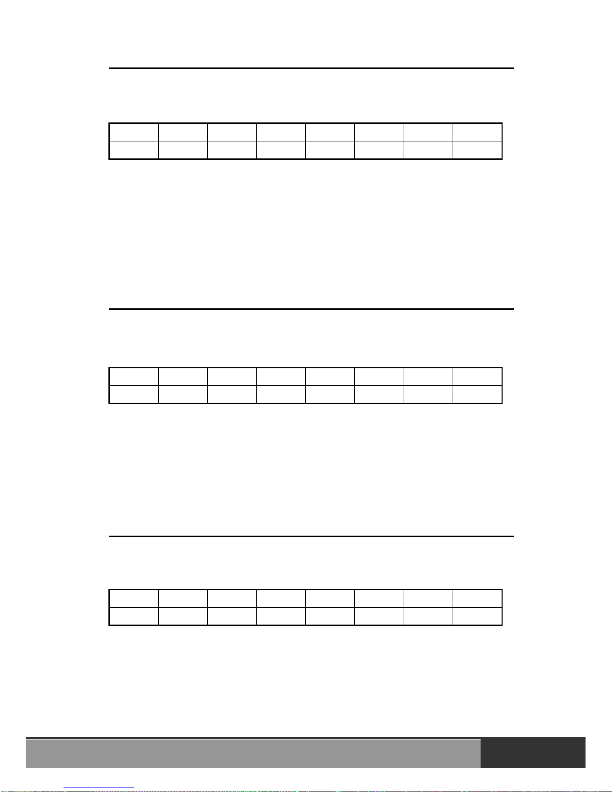
3.3.1 RESET\ Control Register
(Write): wBase+0
Bit 7
Bit 6
Bit 5
Bit 4
Bit 3
Bit 2
Bit 1
Bit 0
Reserved
Reserved
Reserved
Reserved
Reserved
Reserved
Reserved
RESET\
When the PC is first powered-on, the RESET\ signal is in the Low-state. This
will disable all D/I/O operations. The user has to set the RESET\ signal to the
High-state before performing any D/I/O commands.
outportb (wBase,1); /*RESET\=High all D/I/O operations are enable now */
outportb (wBase,0); /*RESET\=Low all D/I/O operations are disable now */
3.3.2 AUX Control Register
(Write): wBase+2
Bit 7
Bit 6
Bit 5
Bit 4
Bit 3
Bit 2
Bit 1
Bit 0
Aux7
Aux6
Aux5
Aux4
Aux3
Aux2
Aux1
Aux0
Aux?=0 this Aux is used as a D/I
Aux?=1 this Aux is used as a D/O
When the PC is first powered-on, all Aux signals are in the Low-state. All Aux
are designed as D/I operations for all PIO/PISO series cards.
3.3.3 AUX Data Register
(Read/Write): wBase+3
Bit 7
Bit 6
Bit 5
Bit 4
Bit 3
Bit 2
Bit 1
Bit 0
Aux7
Aux6
Aux5
Aux4
Aux3
Aux2
Aux1
Aux0
When the Aux is used as D/O operations, the output state is controlled by this
register. This register is designed for use with future extensions. Therefore, do
not use this register.
Page 32
PIO/PEX-D24/D56 Series User Manual (Ver.3.1, Mar. 2015, PMH-005-31) 32
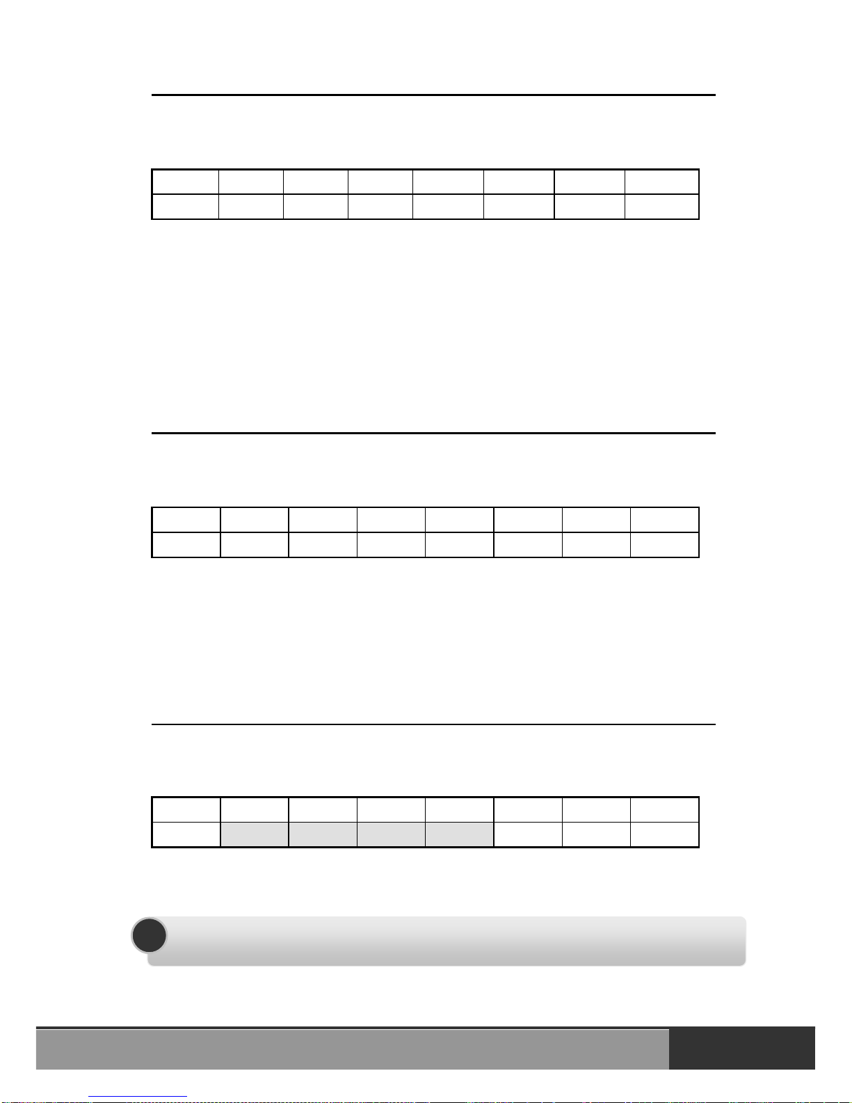
3.3.4 INT Mask Control Register
(Write): wBase+5
Bit 7
Bit 6
Bit 5
Bit 4
Bit 3
Bit 2
Bit 1
Bit 0
0 0 0 0 EN3
EN2
EN1
EN0
EN0=0 Disable P2C0 as a interrupt signal (Default).
EN0=1 Enable P2C0 as a interrupt signal
outp(wBase+5,0); /* Disable interrupt */
outp(wBase+5,1); /* Enable interrupt P2C0 */
outp(wBase+5,0x0f); /* Enable interrupt P2C0, P2C1, P2C2, and P2C3 */
3.3.5 Aux Status Register
(Read): wBase+7
Bit 7
Bit 6
Bit 5
Bit 4
Bit 3
Bit 2
Bit 1
Bit 0
Aux7
Aux6
Aux5
Aux4
Aux3
Aux2
Aux1
Aux0
Aux0=P2C0, Aux1=P2C1, Aux2=P2C2, Aux3=P2C3, Aux7~4=Aux-ID. Refer to
the DEMO5.C file for more information. Aux 0~3 are used as interrupt sources.
The interrupt service routine must read this register to identify the interrupt
source. Refer to Sec. 2.5 for more information.
3.3.6 Read Card ID Register
(Read): wBase+0xcc
Bit 7
Bit 6
Bit 5
Bit 4
Bit 3
Bit 2
Bit 1
Bit 0
0
ID3
ID2
ID1
ID0
Port2
Port1
Port0
wCardID = inportb(wBase+0xcc) >>3; /* Read Card ID */
Note: The Card ID function is only supported by the PIO-D24U/D56U and
PEX-D24/D56 (Ver1.0 or above)
!
Page 33
PIO/PEX-D24/D56 Series User Manual (Ver.3.1, Mar. 2015, PMH-005-31) 33
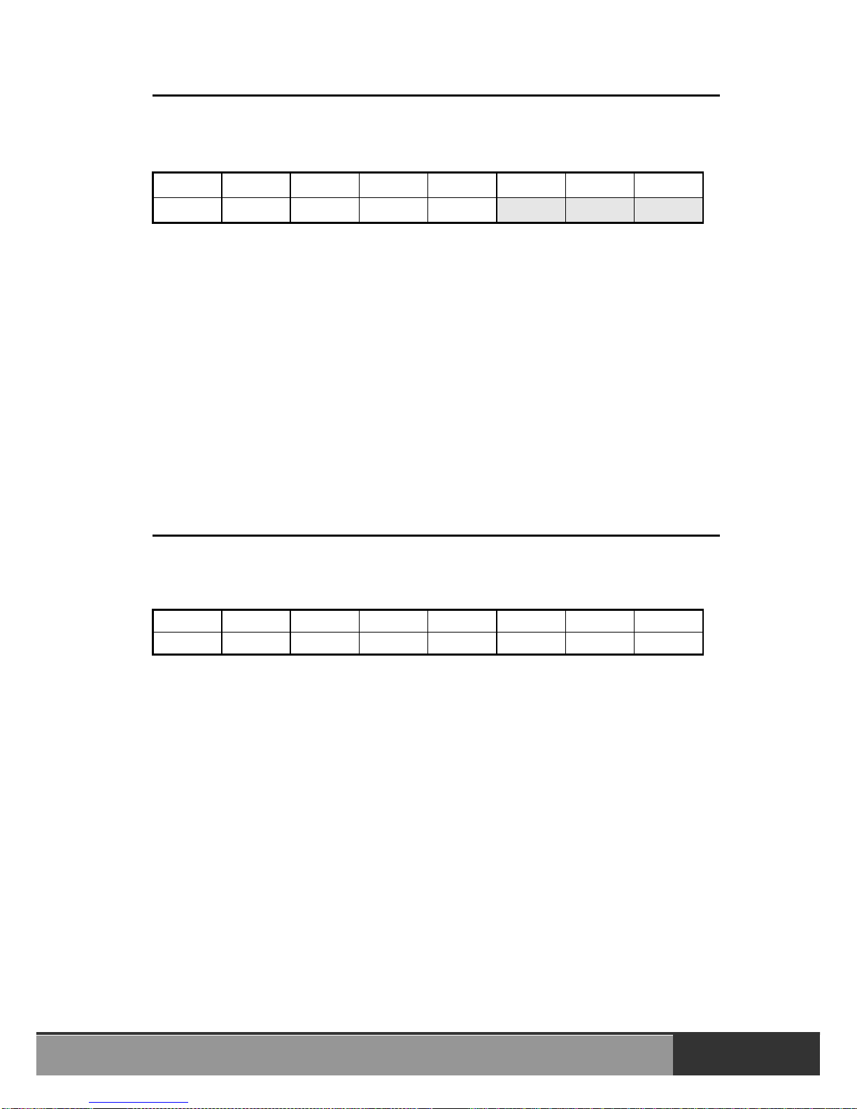
3.3.7 I/O Selection Control Register
(Write): wBase+0xcc
Bit 7
Bit 6
Bit 5
Bit 4
Bit 3
Bit 2
Bit 1
Bit 0
0
ID3
ID2
ID1
ID0
Port2
Port1
Port0
This registers provide the function for configuration the digital input/output ports
of the PIO/PISO series cards. Every I/O port can be programmed to either a D/I
or a D/O port. Note that all ports are set as D/I ports when the PC is first
powered-on.
Port? = 1 this port is used as a D/O port
Port? = 0 this port is used as a D/I port
outportb(wBase+0xcc,0x00); /* Set Port 0/1/2 as D/I port */
outportb(wBase+0xcc,0x04); /* Set Port0/1 as D/I port */
/* Set Port2 as D/O port */
3.3.8 Interrupt Polarity Control Register
(Write): wBase+0x2a
Bit 7
Bit 6
Bit 5
Bit 4
Bit 3
Bit 2
Bit 1
Bit 0
0 0 0 0 INV3
INV2
INV1
INV0
This register provides a function that is used to control whether the interrupt
signal source is inverted or non-inverted. A detailed application example is
shown below.
INV0=1 select the non-inverted signal from P2C0
INV0=0 select the inverted signal from P2C0
outportb(wBase+0x2a,0x0f); /*Select the non-inverted input P2C0/1/2/3 */
outportb(wBase+0x2a,0x00); /*Select the inverted input of P2C0/1/2/3 */
outportb(wBase+0x2a,0x0e); /*Select the inverted input of P2C0 */
/*Select the non-inverted input P2C1/2/3 */
outportb(wBase+0x2a,0x0c); /*Select the inverted input of P2C0/1 */
/*Select the non-inverted input P2C2/3 */
Refer to Sec. 2.5 and DEMO5.C for more information.
Page 34
PIO/PEX-D24/D56 Series User Manual (Ver.3.1, Mar. 2015, PMH-005-31) 34
3.3.9 Read/Write 8-bit data Register
(Read/Write):wBase+0xc0/0xc4/0xc8/0xd0/0xd4
Bit 7
Bit 6
Bit 5
Bit 4
Bit 3
Bit 2
Bit 1
Bit 0
D7
D6
D5
D4
D3
D2
D1
D0
The PIO-D24/D56 and PEX-D24/D56 series contains 5/3 8-bit I/O ports, and
each I/O port can be configured as either a D/I or a D/O port. The user can
send/receive digital data to/from this register for digital input or output. Note that
all ports are set as D/I ports when the PC is first powered-on.
outportb(wBase+0xc0,Val); /*Write to port-0 */
Val=inportb(wBase+0xc0); /*Read from port-0*/
outportb(wBase+0xcc,0x07); /*Set Port0~Port2 as DO port */
outportb(wBase+0xc0,i1); /*Write to Port0 */
outportb(wBase+0xc4,i2); /*Write to Port1 */
outportb(wBase+0xc8,i3); /*Write to Port2 */
outportb(wBase+0xcc,0x01); /*Set Port0 as DO port */
/*port1~Port2 as DI port */
outportb(wBase+0xc0,i1); /*Write to Port0 */
j2=inportb(wBase+0xc4); /*Read Port1 */
j3=inportb(wBase+0xc8); /*Read Port2 */
L=inportb(wBase+0xd0); /*Read CON2 Low byte */
H=inportb(wBase+0xd4); /*Read CON2 High byte */
Val=(H<<8)+L ; /*Val is 16 bit data */
outportb(wBase+0xd0,Val); /*Write to CON1 Low byte */
outportb(wBase+0xd4,(Val>>8)); /*Write to CON1 high byte */
Note: Make sure the I/O port configuration (DI or DO) before read/write
the data register (wBase+0xc0/0xc4/0xc8), refer to Sec.3.3.7 and Table
3.3 for more information.
!
Page 35
PIO/PEX-D24/D56 Series User Manual (Ver.3.1, Mar. 2015, PMH-005-31) 35
4. Software Installation
The PIO-D24/D56 and PEX-D24/D56 series can be used in DOS and Windows
98/ME/NT/2K and 32-bit/64-bit Windows XP/2003/Vista/7. The recommended
installation procedure for windows is given in Sec. 4.1 ~ 4.2. Or refer to Quick
Start Guide (CD:\NAPDOS\PCI\PIO-DIO\Manual\QuickStart\).
http://ftp.icpdas.com/pub/cd/iocard/pci/napdos/pci/pio-dio/manual/quickstart/
4.1 Software Installing Procedure
UniDAQ SDK driver (32-bit/64-bit Windows XP/2003/Vista/7):
Step 1: Insert the companion CD into the CD-ROM drive and after a few
seconds the installation program should start automatically. If it
doesn’t start automatically for some reason, double-click the
AUTO32.EXE file in the NAPDOS folder on this CD.
Step 2: Click the item: “PCI Bus DAQ Card”.
Step 3: Click the item: “UniDAQ”.
Step 4: Click the item: “DLL for Windows 2000 and XP/2003/Vista 32-bit”.
Step 5: Double-Click “UniDAQ_Win_Setup_x.x.x.x_xxxx.exe” file in the
Driver folder.
Windows driver (Windows 98/NT/2K and 32-bit Windows XP/2003/Vista/7):
Step 1: Insert the companion CD into the CD-ROM drive and after a few
seconds the installation program should start automatically. If it
doesn’t start automatically for some reason, double-click the
AUTO32.EXE file in the NAPDOS folder on this CD.
Step 2: Click the item: “PCI Bus DAQ Card”.
Step 3: Click the item: “PIO-DIO”.
Step 4: Click the item “DLL and OCX for Windows 98/NT/2K/XP/2003”.
Step 5: Double-Click “PIO_DIO_Win_vxxx.exe” file in the Driver folder.
Page 36
PIO/PEX-D24/D56 Series User Manual (Ver.3.1, Mar. 2015, PMH-005-31) 36
The setup program will then start the driver installation and copy the relevant
files to the specified directory and register the driver on your computer. The
directory where the drive is stoned is different for different windows versions, as
shown below.
Windows 64-bit Windows XP/2003/Vista/7:
The UniDAQ.DLL file will be copied into the C:\WINNT\SYSTEM32 folder
The NAPWNT.SYS and UniDAQ.SYS files will be copied into the
C:\WINNT\SYSTEM32\DRIVERS folder
For more detailed UniDAQ.DLL function information, please refer to
UniDAQ SDK user manual (CD:\NAPDOS\PCI\UniDAQ\Manual\).
http://ftp.icpdas.com/pub/cd/iocard/pci/napdos/pci/unidaq/maunal/
Windows NT/2K and 32-bit Windows XP/2003/Vista/7:
The PIODIO.DLL file will be copied into the C:\WINNT\SYSTEM32 folder
The NAPWNT.SYS and PIO.SYS files will be copied into the
C:\WINNT\SYSTEM32\DRIVERS folder
Windows 95/98/ME:
The PIODIO.DLL and PIODIO.Vxd files will be copied into the
C:\Windows\SYSTEM folder
For more detailed PIODIO.DLL function information, please refer to
“PIO-DIO DLL Software Manual.pdf(CD:\NAPDOS\PCI\PIO-DIO\Manual\)”.
http://ftp.icpdas.com/pub/cd/iocard/pci/napdos/pci/pio-dio/manual/
4.2 PnP Driver Installation
Power off the computer and install the PIO-D24/D56 and PEX-D24/D56 series
cards. Turn on the computer and Windows 98/Me/2K and 32-bit/64-bit Windows
XP/2003/Vista/7 should automatically defect the new PCI device(s) and then
ask for the location of the driver files for the hardware. If a problem is
encountered during installation, refer to the PnPinstall.pdf file for more
information.
!
!
Page 37
PIO/PEX-D24/D56 Series User Manual (Ver.3.1, Mar. 2015, PMH-005-31) 37
4.3 Confirm the Successful Installation
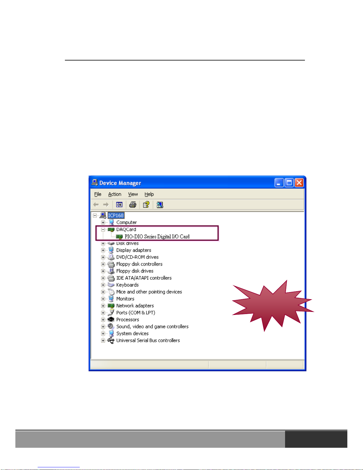
Make sure the PIO-D24/D56 or PEX-D24/D56 series cards installed are correct
on the computer as follows:
Step 1: Select “Start” “Control Panel” and then double click the “System”
icon on Windows.
Step 2: Click the “Hardware” tab and then click the “Device Manager” button.
Step 3: Check the PIO-DIO series card which listed correctly or not, as
illustrated below.
Successful
Page 38
PIO/PEX-D24/D56 Series User Manual (Ver.3.1, Mar. 2015, PMH-005-31) 38
BCB 4 for Borland C
++
Builder 4
PIODIO.H Header files
PIODIO.LIB Linkage library for BCB only
Delphi4 for Delphi 4
PIODIO.PAS Declaration files
VB6 for Visual Basic 6
PIODIO.BAS Declaration files
VC6 for Visual C++ 6
PIODIO.H Header files
PIODIO.LIB Linkage library for VC only
VB.NET2005 for VB.NET2005
PIODIO.vb Visual Basic Source files
CSharp2005 for C#.NET2005
PIODIO.cs Visual C# Source files
5. Demo Programs for Windows
None of the demo programs will function correctly if the DLL driver is not
properly installed. During the DLL driver installation process, the Install Shield
software will register the correct kernel driver to the operating system and copy
the DLL driver and demo programs to the correct position based on the driver
software package you have selected (Win98/ME/NT/2K and 32-bit Windows
XP/2003/Vista/7). After the drivers are installed, the relevant demo programs,
development libraries and declaration header files for the different development
environments will be available in the following locations.
The demo program is contained in:
CD:\NAPDOS\PCI\PIO-DIO\DLL_OCX\Demo\
http://ftp.icpdas.com/pub/cd/iocard/pci/napdos/pci/pio-dio/dll_ocx/demo/
A list of available demo programs is as follows:
DIO: Digital input and output
DIO_2: Digital input and output (only for PIO-D56(U)/PEX-D56 )
INT: Interrupt test
INTAPC: Interrupt test
Page 39
PIO/PEX-D24/D56 Series User Manual (Ver.3.1, Mar. 2015, PMH-005-31) 39
TC\*.* for Turbo C 2.xx or above
TC\LIB\*.* for TC library
TC\DEMO\*.* for TC demo programs
TC\DIAG\*.* for TC diagnostic programs
TC\LIB\PIO.H TC declaration file
TC\\LIB\TCPIO_L.LIB TC large model library file
TC\\LIB\TCPIO_H.LIB TC huge model library file
MSC\*.* for MSC 5.xx or above
MSC\LIB\PIO.H MSC declaration file
MSC\\LIB\MSCPIO_L.LIB MSC large model library file
MSC\\LIB\MSCPIO_H.LIB MSC huge model library file
BC\*.* for BC 3.xx or above
BC\LIB\PIO.H BC declaration file
BC\\LIB\BCPIO_L.LIB BC large model library file
BC\\LIB\BCPIO_H.LIB BC huge model library file
Appendix
Appendix A. Related DOS Software
A1. Where is the related software
The related DOS software and demos are located on the CD as below:
CD:\NAPDOS\PCI\PIO-DIO\dos\
http://ftp.icpdas.com/pub/cd/iocard/pci/napdos/pci/pio-dio/dos/
The list of demo programs:
DEMO1: D/O for CON1
DEMO2: D/I/O for CON1 ~ CON3
DEMO3: Interrupt of P2C0 (Initial low and active high)
DEMO4: Interrupt of P2C0 (Initial high and active low)
DEMO5: 4 interrupt sources
Page 40
PIO/PEX-D24/D56 Series User Manual (Ver.3.0, Feb. 2011, PMH-005-30 ) 40
A2. DOS LIB Functions
A2-1. ErrorCode and ErrorString Code Table
Table A.1
Error
Code
Error ID
Error String
0
NoError
OK (No error)
1
Driver HandleError
Error opening the device driver
2
DriverCallError
An error occurred while calling the driver
functions
3
FindBoardError
Can’t find the board on the system
4
TimeOut
Timeout
5
ExeedBoardNumber
Invalid board number
(Valid range: 0 to TotalBoards -1)
6
NotFoundBoard
Can’t detect the board on the system
A2-2. PIO_DriverInit
Description:
This function is used to detect all PIO/PISO series card in the system
and is implemented based on the PCI Plug & Play mechanism. The
function will locate/identify all PIO/PISO series cards installed in this
system and save the resource information in the library.
Syntax:
WORD PIO_DriverInit(WORD *wBoards, WORD wSubVendorID,
WORD wSubDeviceID, WORD wSubAuxID)
Parameters:
WBoards
[Output]
The number of boards found in this PC
wSubVendorID
[Input]
SubVendor ID of the board
wSubDeviceID
[Input]
SubDevice ID of the board
wSubAuxID
[Input]
SubAux ID of the board
Returns:
Refer to "Table A.1".
Page 41
PIO/PEX-D24/D56 Series User Manual (Ver.3.0, Feb. 2011, PMH-005-30 ) 41
A2-3. PIO_GetConfigAddressSpace
Description:
This function can be used to save the resource information all PIO/PISO
cards installed in the system. The application program can then control
all the functions of the PIO/PISO series card directly.
Syntax:
WORD PIO_GetConfigAddressSpace(wBoardNo,*wBase,*wIrq,
wSubVendor, *wSubDevice, *wSubAux, *wSlotBus, *wSlotDevice)
Parameters:
wBoardNo
[Input]
The board number
wBase
[Output]
The base address of the board
wIrq
[Output]
The IRQ number that the board using
wSubVendor
[Output]
Sub Vendor ID
wSubDevice
[Output]
Sub Device ID
wSubAux
[Output]
Sub Aux ID
wSlotBus
[Output]
Slot Bus number
wSlotDevice
[Output]
Slot Device ID
Returns:
Refer to "Table A.1".
A2-4. PIO_GetDriverVersion
Description:
This function is used to obtain the version number of PIODIO driver.
Syntax:
WORD PIO_GetDriverVersion(WORD *wDriverVersion)
Parameters:
wDriverVersion
[Output]
wDriverVersion address
Returns:
Refer to "Table A.1".
Page 42
PIO/PEX-D24/D56 Series User Manual (Ver.3.0, Feb. 2011, PMH-005-30 ) 42
A2-5. ShowPIOPISO
Description:
This function can be used to display a text string indicating the special
Sub_ID. This text string is the same as that defined in PIO.H.
Syntax:
WORD ShowPIOPISO(wSubVendor, wSubDevice, wSubAux)
Parameters:
wSubVendor
[Input]
SubVendor ID of the board
wSubDevice
[Input]
SubDevice ID of the board
wSubAux
[Input]
SubAux ID of the board
Returns:
Refer to "Table A.1".
 Loading...