

ICPDAS I-7521, I-7522, I-7522A, I-7527, I-7524 User Manual
...
I-7521/I-7522/I-7522A/I-7523/I-7524/I-7527 User’s Manual,Ver2.5 Aug.2015
1
I-7521/I-7522/I-7522A/I-7523/I-7524
/I-7527
User’s Manual
Warranty
All products manufactured by ICP DAS are warranted against defective materials for a
period of one year from the date of delivery to the original purchaser.
Warning
ICP DAS assume no liability for damages resulting from the use of this product. ICP
DAS reserves the right to change this manual at any time without notice. The
information furnished by ICP DAS is believed to be accurate and reliable. However, no
responsibility is assumed by ICP DAS for its use, nor for any infringements of patents
or other rights of third parties resulting from its use.
Copyright
Copyright 2006 by ICP DAS. All rights are reserved.
Trademark
The names used for identification only may be registered trademarks of their respective
companies.
World Wide Web Home Page and FTP Site
To access ICPDAS home page go to http://www.icpdas.com
To download document and software go to http://www.icpdas.com/download/752n.htm
or ftp://ftp.icpdas.com.tw/pub/cd/8000cd/napdos/752n/
Technical Support
Questions and requests can be sent via E-mail to service@icpdas.com

I-7521/I-7522/I-7522A/I-7523/I-7524/I-7527 User’s Manual,Ver2.5 Aug.2015
2
TABLE OF COMTENTS
CHAPTER 1 INTRODUCTION ........................................................................... 4
1.1. OVERVIEW ................................................................................................ 4
1.2. FEATURES ................................................................................................. 8
1.3. DIMENSIONS ............................................................................................. 9
1.4. PIN ASSIGNMENT .................................................................................... 11
1.5. SPECIFICATIONS ..................................................................................... 23
1.6. WIRING DIAGRAMS FOR APPLICATION ................................................. 25
1.6.1. Program download ................................................................. 25
1.6.2. Using a 3-wire RS-232 port ................................................... 26
1.6.3. Using a 5-wire RS-232 port ................................................... 27
1.6.4. Using a RS-485 port ............................................................... 28
1.6.5. Using DI/DO of I-7521(D) ...................................................... 29
1.6.6. Using DI/DO of I-7522A(D) ................................................... 30
1.6.7. Using a RS-485 of I-7522A(D) ............................................... 31
1.7. COMPARISON TABLE .............................................................................. 32
CHAPTER 2 OPERATING PRINCIPLES.......................................................... 34
2.1 INIT* PIN OPERATING PRINCIPLES ........................................................ 34
2.2 DEMO CODE, FIRMWARE AND 7188XW.EXE.......................................... 36
2.3 THE RS-485 PORT AND SELF-TURNER ASIC ........................................ 37
2.4 7-SEGMENT LED DISPLAY ..................................................................... 37
2.5 752N PROTOCOL DESCRIPTION .............................................................. 38
2.6 WRITING PROGRAM ON 752N ................................................................ 43
CHAPTER 3 QUICK START ............................................................................. 44
3.1 CONNECTING THE I-752N MODULE ....................................................... 45
3.2 CONNECTING TO A SINGLE REMOTE RS-232 DEVICE .......................... 52
3.3 CONNECTING TO MULTIPLE REMOTE RS-232 DEVICE ........................ 57
3.4 DOWNLOADING NEW FIRMWARE TO THE I-752N MODULE ................. 60
3.4.1. Using MiniOS7 Utility to download new firmware ............. 60
3.4.2. Using 7188xw.exe to download a file .................................... 62
CHAPTER 4 DI/DO AND WATCHDOG ........................................................... 63
4.1 DO OPERATION PRINCIPLES ................................................................. 63
4.2 DI OPERATION PRINCIPLES ................................................................... 63
4.3 DUAL WATCHDOG OPERATION PRINCIPLES ........................................ 64
4.4 HOST WATCHDOG APPLICATION NOTES .............................................. 64
4.5 MODULE WATCHDOG APPLICATION NOTES ........................................ 66
CHAPTER 5 COMMAND SETS ........................................................................ 67
5.1 COMMAND SET TABLE ........................................................................... 67
5.2 ADDRESS MAPPING TABLE .................................................................... 68
5.3 COMMANDS ............................................................................................. 69

I-7521/I-7522/I-7522A/I-7523/I-7524/I-7527 User’s Manual,Ver2.5 Aug.2015
3
5.3.1 $AAA[addr] ............................................................................ 69
5.3.2 $AABN[baud rate] ................................................................. 70
5.3.3 $AADN[data-bit] .................................................................... 72
5.3.4 $AAPN[parity-bit] ................................................................. 74
5.3.5 $AAON[stop-bit] .................................................................... 76
5.3.6 $AA6[ID] ................................................................................. 78
5.3.7 $AA7 ........................................................................................ 79
5.3.8 $AAC[delimiter] ..................................................................... 80
5.3.9 $AAD ....................................................................................... 81
5.3.10 [delimiter]AA[bypass]............................................................ 82
5.3.11 $AAKV .................................................................................... 83
5.3.12 $AATN[CrLfmode] ................................................................ 84
5.3.13 $AAW ...................................................................................... 86
5.3.14 $AAXV .................................................................................... 87
5.3.15 $AAYN .................................................................................... 88
5.3.16 $AAZNV ................................................................................. 89
5.3.17 #** ........................................................................................... 91
5.3.18 $AA4 ........................................................................................ 92
5.3.19 $AA5 ........................................................................................ 94
5.3.20 $AAF ....................................................................................... 96
5.3.21 $AAM ...................................................................................... 97
5.3.22 $AA2 ........................................................................................ 98
5.3.23 ~** ........................................................................................... 99
5.3.24 ~AA0 ...................................................................................... 100
5.3.25 ~AA1 ...................................................................................... 101
5.3.26 ~AA2 ...................................................................................... 103
5.3.27 ~AA3ETT .............................................................................. 105
5.3.28 ~AA4P & ~AA4S .................................................................. 106
5.3.29 ~AA5P & ~AA5S .................................................................. 107
5.3.30 $AAU ..................................................................................... 108
5.3.31 $AAL[data] ........................................................................... 110
5.3.32 $AAR ..................................................................................... 112
5.3.33 $AAJN[timeout] ................................................................... 113
5.3.34 $AAGN[triggerlevel] ............................................................ 115
5.3.35 @AA[data] ............................................................................ 116
5.3.36 #AABBHH ............................................................................ 118
5.3.37 #AABCDD ............................................................................ 119
5.3.38 $AAEV .................................................................................. 120
5.3.39 $AAHV .................................................................................. 122
5.3.40 $AAIV ................................................................................... 124
CHAPTER 6 APPLICATIONS ......................................................................... 125
6.1. CNNECTING TO THE HP34401A ........................................................... 125
6.1.1 Connect the I-752N module to the HP34401A ................... 125
6.1.2 Connecting a PC to the HP34401A ..................................... 125
6.1.3 Connecting a single I-7522 to a single HP34401A ............. 127
6.1.4 Connecting multiple I-7522 modules and multiple HP34401A
129
6.1.5 Connecting a single I-7523 modules and two HP34401A .. 131
6.1.6 Connecting multiple I-7523 modules and multiple HP34401A
133
6.2. TYPICAL APPLICATIONS ...................................................................... 135
APPENDIX A MINIOS7 UTILITY ................................................................................. 142
APPENDIX B 7188XW.EXE ........................................................................................... 143
APPENDIX C FIRMWARE VERSION INFORMATION ............................................. 148

I-7521/I-7522/I-7522A/I-7523/I-7524/I-7527 User’s Manual,Ver2.5 Aug.2015
4
Chapter 1 Introduction
Nowadays, a great number of RS-232 devices for both automation
and information transfer are being used in industrial applications, and
linking these devices is very important in the modern situation. The
devices are usually located at a distance from the Host PC, meaning
that linking via multiple serial cards is inefficient. ICPDAS I-752N
series products have been developed to provide an effective link
between multiple RS-232 devices via a single RS-485 network. This
network protocol offers stability, reliability and simple cabling while
delivering a low–cost, easy-to-maintain product.
1.1. Overview
Addressable RS-232 Converter
Most RS-232 devices don’t support individual device addressing. To
overcome this limitation, ICPDAS I-752N series modules assign a
unique address to any RS-232 device installed on an RS-485 network.
When the Host PC sends a command to the RS-485 network a device
address can be attached to the command. The destination I-752N
module will then remove the address field and pass the remaining
commands to the destination RS-232 device. Responses from the
local RS-232 devices will be returned to the Host PC via the I-752N
module.
Responses from RS-232 devices can be addressable
ICPADS I-752N series modules can prefix a response from an RS-232
device with a unique address and then pass the response to the
RS-485 network. The Host PC can then identify which RS-232 device
the response comes from.
Master-type Addressable RS-232 Converter

I-7521/I-7522/I-7522A/I-7523/I-7524/I-7527 User’s Manual,Ver2.5 Aug.2015
5
ICPDAS I-752N products are unique. In that they are Master-type
converters, while most other converters are Slave-type, which are
helpless without a Host PC. In real industrial applications, many users
are not satisfied with Slave-type converters as they cannot be adapted
to individual requirement. The powerful I-752N series analyzes the DI /
DO of local RS-232 devices without the need for a Host PC. Refer to
Applications 7~9 in Sec.6.2 for more information.
Onboard 1Kb Queue buffer
I-752N series modules are equipped while a 1Kb queue buffer for its
local RS-232 device. All input data can be stored in the queue buffer
until the Host PC has time to read it. These features allow the Host PC
to be linked to thousands of RS-232 devices without any loss of data.
(Refer to Sec.5.3.30)
Onboard DI signal trigger
I-752N series modules are equipped with 1/2/5 DI channels for sensor
interfacing. These DI channels are linked to a photo sensor/switch to
act as a signal. They also can be used as general purpose DI. I-752N
series modules provide ODM and applicatin demos for a user to
modify them to read and analyze these DI signals without the need for
a Host PC.
Onboard DO channels for emergency control
I-752N series modules equipped with 1/3/5 DO channels for
emergency control. The DO channels can directly drive either relay or
an LED, and can be used to control the local devices in the event of an
emergency. I-752N series modules provide ODM and applicatin
demos for a user to modify them to control these DO channels without
the need for a Host PC.
3000V isolation on the RS-485 side
I-7521/I-7522/I-7522A/I-7523/I-7524/I-7527 User’s Manual,Ver2.5 Aug.2015
6
COM2 of the I-7521/I-7522/I-7523 modules is an isolated RS-485 port
with 3000V isolation, which will protect the local RS-232 devices from
transient noises coming from the RS-485 network.
Self-Tuner ASIC inside
The interned I-752N Self-Tuner ASIC for the RS-485 port can auto
detect and control the send/receive direction of the RS-485 network,
meaning that there is no need for application programs to be
concerned about direction control of the RS-485 network.
A Wide range available for selection
RS-232
RS-485
RS-232/
RS-485
RS-422/
RS-485
DI
DO
I-7521(D)
1 1 2
3
I-7522(D)
1 1 1 2
1
I-7523(D)
2 1 1 1
0
I-7522A(D)
1 1 1 5
5
I-7524(D)
3 1 1 1
1
I-7527(D)
6 1 1 1
1
Note: I-752N means any one of seven kinds of modules above.
Order Information
Order item choice
Order item
Module name
O.S
I-7521(D)
Intelligent communication controller
(1 channel of RS-232)
MiniOS7
I-7522(D)
Intelligent communication controller
(2 channel of RS-232)
MiniOS7
I-7523(D)
Intelligent communication controller
(3 channel of RS-232 )
MiniOS7
I-7522A(D)
Intelligent communication controller
(1 channel of RS-232 and 1 channel
Of RS-422/485)
MiniOS7
I-7524(D)
Intelligent communication controller
MiniOS7

I-7521/I-7522/I-7522A/I-7523/I-7524/I-7527 User’s Manual,Ver2.5 Aug.2015
7
(4 channel of RS-232)
I-7527(D)
Intelligent communication controller
(7 channel of RS-232)
MiniOS7
I-7XXX
I-7XXX without 7-SEG display
MiniOS7
I-7XXXD
I-7XXX with 7-SEG display
MiniOS7
Package List
The package includes the following item:
One I-7521/I-7522/I-7522A/I-7523/I-7524/I-7527 User’s
Manual (this manual)
One release note(Depend on situation)
One software utility disk or CD
One download cable CA0910F for I-7521, I-7522, I-7523
CA0910 for I-7522A, I-7524, I-7527
Note:
If any of these items are missing or damaged, contact the local
distributors for more information. Save the shipping materials
and cartons in case you want to ship in the future.
Release Note (Important):
It is recommended to read the release note first. All important
information will be given in release note as follows:
Influential modification about software or hardware
The path that points to I-752N document and software
changes in the companion CD
others……….

I-7521/I-7522/I-7522A/I-7523/I-7524/I-7527 User’s Manual,Ver2.5 Aug.2015
8
1.2. Features
General
Built-in “Addressable RS-232 Converter” firmware
Supports Dual-Watchdog commands
Supports Power-up value & safe value for DO
The firmware code is open source and well documented
Source code could be modified depending on according specific
user requirements.
The firmware can monitor the onboard DI and control the onboard
DO in real-time depending on user requirements
The firmware can monitor the RS-232 device and control the
onboard DO in real-time according to user’s requirements
Watchdog timer provides fault tolerance and recovery
Low power consumption
R.O.C. Invention Patent No. 086674
R.O.C. Invention Patent No. 103060
R.O.C. Patent No. 132457
I-7521/I-7522/I-7522A/I-7523/I-7524/I-7527 User’s Manual,Ver2.5 Aug.2015
9
1.3. Dimensions
For I-7521(D)/I-7522(D)/I-7523(D)
I-7521/I-7522/I-7522A/I-7523/I-7524/I-7527 User’s Manual,Ver2.5 Aug.2015
10
For I-7522A(D)/I-7524(D)/I-7527(D)
I-7521/I-7522/I-7522A/I-7523/I-7524/I-7527 User’s Manual,Ver2.5 Aug.2015
11
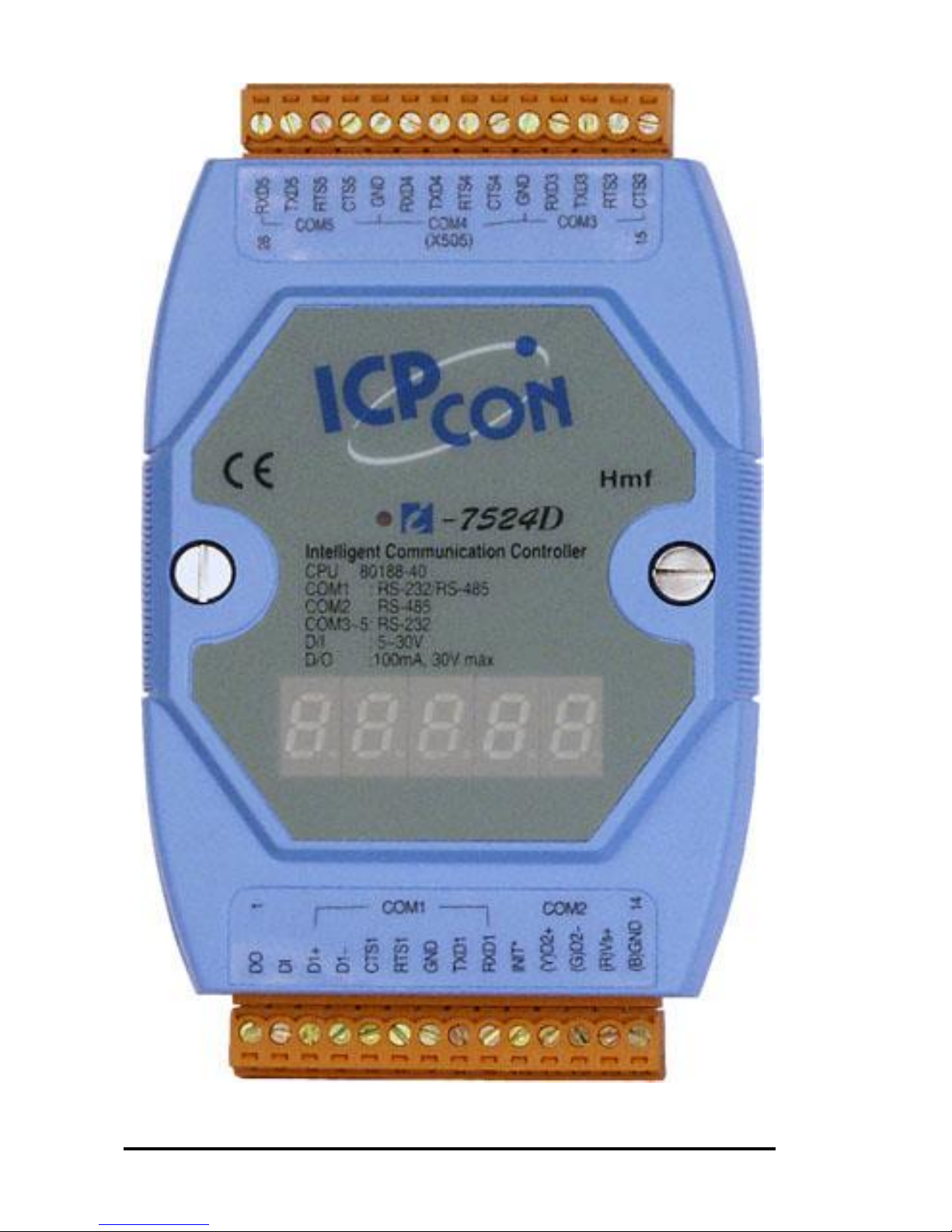
1.4. Pin Assignment

I-7521/I-7522/I-7522A/I-7523/I-7524/I-7527 User’s Manual,Ver2.5 Aug.2015
12
Pin assignment of 13-pin screw terminal block(I-7521/I-7521D):
Pin
Name
Description
1
X3
Connects to I/O expansion board
2
X2
Connects to I/O expansion board
3
X1
Connects to I/O expansion board
4
DO3
Digital output, 150mA, 30V
5
DO2
Digital output, 150mA, 30V
6
DO1
Digital output, 150mA, 30V
7
DI3
Digital input, 3.5V ~ 30V
8
DI2
Digital input, 3.5V ~ 30V
9
INIT*
Initial pin, 3.5V ~ 30V
10
D2+
DATA+ pin of COM2 (RS-485)
11
D2-
DATA- pin of COM2 (RS-485)
12
+VS
V+ of power supply (+10 to +30VDC
unregulated)
13
GND
GND of power supply
Pin assignment of COM1 connector (DB-9 Male):
Pin
Name
Description
1
Data+
DATA+ of RS-485 port
2
TXD
Transmits Data (RS-232)
3
RXD
Receives Data (RS-232)
4
N/C
No Connection
5
GND
Signal ground of RS-232
6
N/C
No Connection
7
CTS
Clear To Send (RS-232)
8
RTS
Request To Send (RS-232)
9
Data-
DATA- of RS-485 port
Note: The COM1 can be used as s RS-232 port or s RS-485 port. It
is not recommended to use both RS-232 & RS-485 at the same
time.
I-7521/I-7522/I-7522A/I-7523/I-7524/I-7527 User’s Manual,Ver2.5 Aug.2015
13

I-7521/I-7522/I-7522A/I-7523/I-7524/I-7527 User’s Manual,Ver2.5 Aug.2015
14
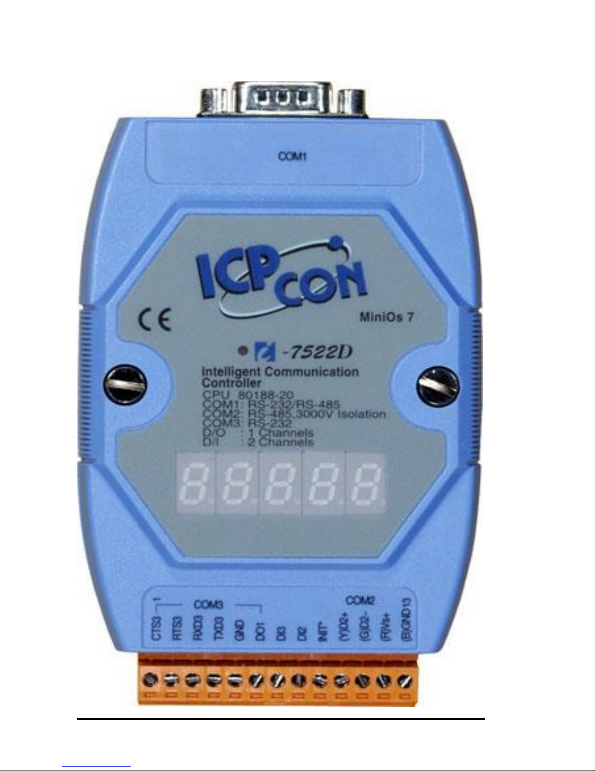
Pin assignment of 13-pin screw terminal block(I-7522/I-7522D):
Pin
Name
Description
1
CTS3
Clear To Send of COM3 (RS-232)
2
RTS3
Request To Send of COM3 (RS-232)
3
RXD3
Receives Data of COM3 (RS-232)
4
TXD3
Transmits Data of COM3 (RS-232)
5
GND
Signal ground of COM3 & COM4
6
DO1
Digital output, 150mA, 30V
7
DI3
Digital input, 3.5V ~ 30V
8
DI2
Digital input, 3.5V ~ 30V
9
INIT*
Initial pin, 3.5V ~ 30V
10
D2+
DATA+ pin of COM2 (RS-485)
11
D2-
DATA- pin of COM2 (RS-485)
12
+VS
V+ of power supply (+10 to +30VDC
unregulated)
13
GND
GND of power supply
Pin assignment of COM1 connector (DB-9 Male):
Pin
Name
Description
1
Data+
DATA+ of RS-485 port
2
TXD
Transmits Data (RS-232)
3
RXD
Receives Data (RS-232)
4
N/C
No Connection
5
GND
Signal ground of RS-232
6
N/C
No Connection
7
CTS
Clear To Send (RS-232)
8
RTS
Request To Send (RS-232)
9
Data-
DATA- of RS-485 port
Note: The COM1 can be used as a RS-232 port or a RS-485 port. It
is not recommended to use both RS-232 & RS-485 at the same
time.
I-7521/I-7522/I-7522A/I-7523/I-7524/I-7527 User’s Manual,Ver2.5 Aug.2015
15

I-7521/I-7522/I-7522A/I-7523/I-7524/I-7527 User’s Manual,Ver2.5 Aug.2015
16
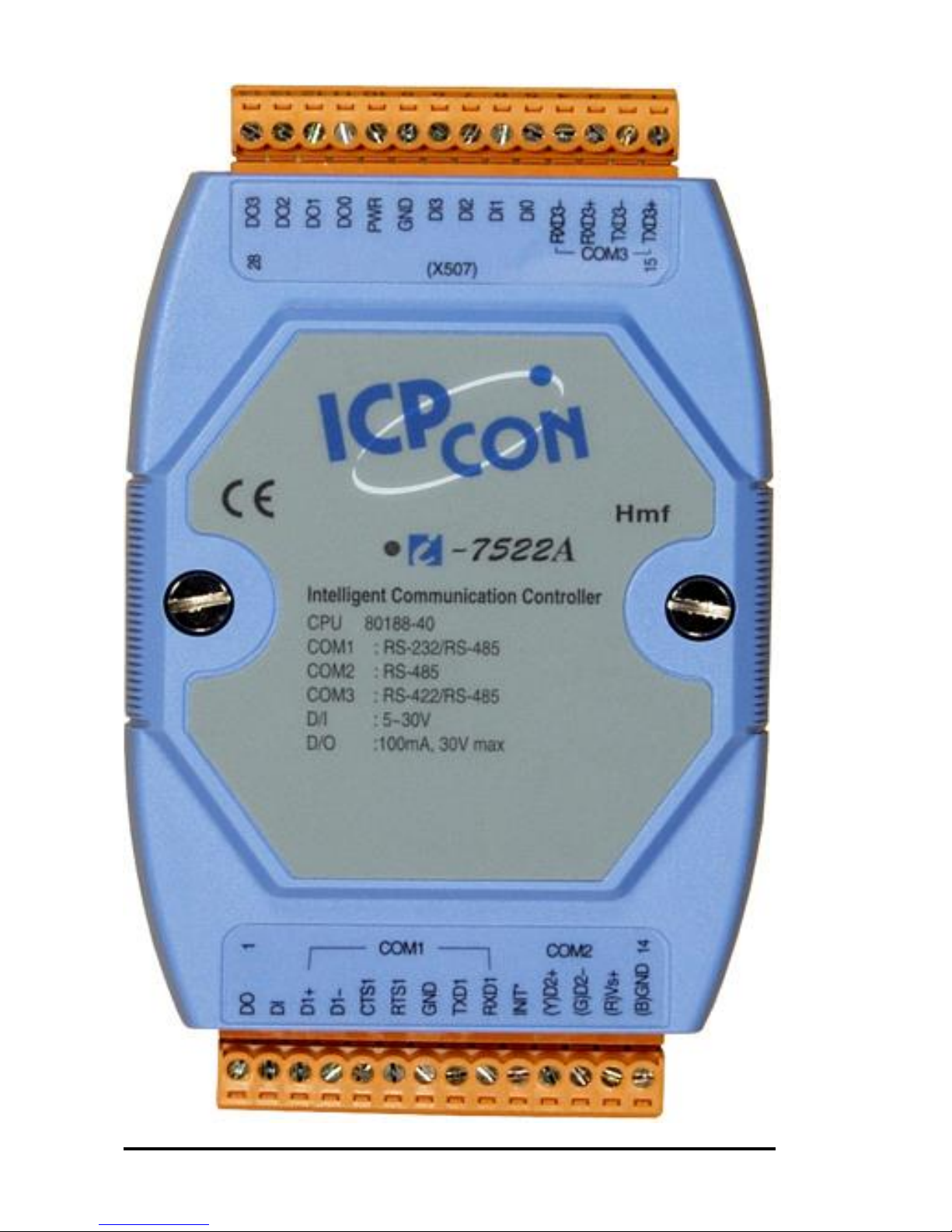
Pin assignment of bottom 14-pin screw terminal block (I-7522A
/I7522AD):
Pin
Name
Description
1
DO
100 mA, 30V max. DO1
2
DI
3.5V ~ 30V,DI1
3
D1+
DATA+ pin of COM1 (RS-485)
4
D1-
DATA - pin of COM1 (RS-485)
5
CTS1
Clear To Send of COM1 (RS-232)
6
RTS1
Request To Send of COM1 (RS-232)
7
GND
Signal ground of RS-232
8
TXD1
Transmits Data of COM1 (RS-232)
9
RXD1
Receives Data of COM1 (RS-232)
10
INIT*
Initial pin, 3.5V ~ 30V
11
D2+
DATA+ pin of COM2 (RS-485)
12
D2-
DATA - pin of COM2 (RS-485)
13
+VS
V+ of power supply (+10 to +30VDC unregulated)
14
GND
GND of power supply
Note: The COM1 can be used as a RS-232 port or a RS-485 port. It is
not recommended to use both RS-232 and RS-485 at the same time.
Pin assignment of top 14-pin screw terminal block:
15
TXD3+
TXD+ pin of COM3 (RS-422/RS-485)
16
TXD3-
TXD - pin of COM3 (RS-422/RS-485)
17
RXD3+
RXD+ pin of COM3 (RS-422)
18
RXD3-
RXD - pin of COM3 (RS-422)
19
DI0
Digital Input, 3.5V ~ 30V, DI2
20
DI1
Digital Input, 3.5V ~ 30V, DI3
21
DI2
Digital Input, 3.5V ~ 30V, DI4
22
DI3
Digital Input, 3.5V ~ 30V, DI5
23
GND
GND of Digital Output
24
PWR
Power of Digital Output
25
DO0
Digital Output, 100 mA, 30V max., DO2
26
DO1
Digital Output, 100 mA, 30V max., DO3
27
DO2
Digital Output, 100 mA, 30V max., DO4
28
DO3
Digital Output, 100 mA, 30V max., DO5
I-7521/I-7522/I-7522A/I-7523/I-7524/I-7527 User’s Manual,Ver2.5 Aug.2015
17
I-7521/I-7522/I-7522A/I-7523/I-7524/I-7527 User’s Manual,Ver2.5 Aug.2015
18
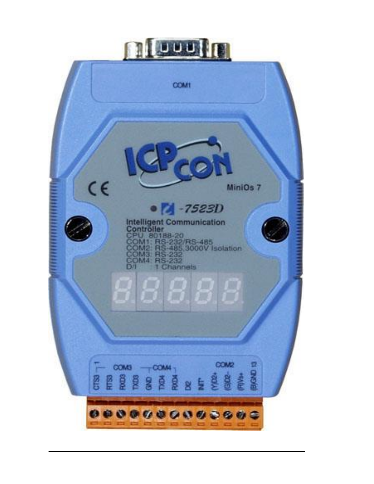
Pin assignment of 13-pin screw terminal block(I-7523/I-7523D):
Pin
Name
Description
1
CTS3
Clear To Send of COM3 (RS-232)
2
RTS3
Request To Send of COM3 (RS-232)
3
RXD3
Receives Data of COM3 (RS-232)
4
TXD3
Transmits Data of COM3 (RS-232)
5
GND
Signal ground of COM3 & COM4
6
TXD4
Transmits Data of COM4 (RS-232)
7
RXD4
Receives Data of COM4 (RS-232)
8
DI2
Digital input, 3.5V ~ 30V
9
INIT*
Initial pin, 3.5V ~ 30V
10
D2+
DATA+ pin of COM2 (RS-485)
11
D2-
DATA- pin of COM2 (RS-485)
12
+VS
V+ of power supply (+10 to +30VDC
unregulated)
13
GND
GND of power supply
Pin assignment of COM1 connector (DB-9 Male):
Pin
Name
Description
1
Data+
DATA+ of RS-485 port
2
TXD
Transmits Data (RS-232)
3
RXD
Receives Data (RS-232)
4
N/C
No Connection
5
GND
Signal ground of RS-232
6
N/C
No Connection
7
CTS
Clear To Send (RS-232)
8
RTS
Request To Send (RS-232)
9
Data-
DATA- of RS-485 port
Note: The COM1 can be used as a RS-232 port or a RS-485 port. It
is not recommended to use both RS-232 and RS-485 at the same
time.
I-7521/I-7522/I-7522A/I-7523/I-7524/I-7527 User’s Manual,Ver2.5 Aug.2015
19

I-7521/I-7522/I-7522A/I-7523/I-7524/I-7527 User’s Manual,Ver2.5 Aug.2015
20
Pin assignment of bottom 14-pin screw terminal block (I-7524/
I-7524D):
Pin
Name
Description
1
DO
100 mA, 30V max.
2
DI
3.5V ~ 30V
3
D1+
DATA+ pin of COM1 (RS-485)
4
D1-
DATA - pin of COM1 (RS-485)
5
CTS1
Clear To Send of COM1 (RS-232)
6
RTS1
Request To Send of COM1 (RS-232)
7
GND
Signal ground of RS-232
8
TXD1
Transmits Data of COM1 (RS-232)
9
RXD1
Receives Data of COM1 (RS-232)
10
INIT*
Initial pin, 3.5V ~ 30V
11
D2+
DATA+ pin of COM2 (RS-485)
12
D2-
DATA - pin of COM2 (RS-485)
13
+VS
V+ of power supply (+10 to +30VDC unregulated)
14
GND
GND of power supply
Note: The COM1 can be used as a RS-232 port or a RS-485 port. It is
not recommended to use both RS-232 & RS-485 at the same time.
Pin assignment of top 14-pin screw terminal block:
15
CTS3
CTS pin of COM3 (RS-232)
16
RTS3
RTS pin of COM3 (RS-232)
17
TXD3
TXD pin of COM3 (RS-232)
18
RXD3
RXD pin of COM3 (RS-232)
19
GND
GND pin of COM3/COM4 (RS-232)
20
CTS4
CTS pin of COM4 (RS-232)
21
RTS4
RTS pin of COM4 (RS-232)
22
TXD4
TXD pin of COM4 (RS-232)
23
RXD4
RXD pin of COM4 (RS-232)
24
GND
GND pin of COM4/5 (RS-232)
25
CTS5
CTS pin of COM5 (RS-232)
26
RTS5
RTS pin of COM5 (RS-232)
27
TXD5
TXD pin of COM5 (RS-232)
28
RXD5
RXD pin of COM5 (RS-232)
I-7521/I-7522/I-7522A/I-7523/I-7524/I-7527 User’s Manual,Ver2.5 Aug.2015
21
I-7521/I-7522/I-7522A/I-7523/I-7524/I-7527 User’s Manual,Ver2.5 Aug.2015
22
Pin assignment of bottom 14-pin screw terminal block:
Pin
Name
Description
1
DO
100 mA, 30V max.
2
DI
3.5V ~ 30V
3
D1+
DATA+ pin of COM1 (RS-485)
4
D1-
DATA - pin of COM1 (RS-485)
5
CTS1
Clear To Send of COM1 (RS-232)
6
RTS1
Request To Send of COM1 (RS-232)
7
GND
Signal ground of RS-232
8
TXD1
Transmits Data of COM1 (RS-232)
9
RXD1
Receives Data of COM1 (RS-232)
10
INIT*
Initial pin, 3.5V ~ 30V
11
D2+
DATA+ pin of COM2 (RS-485)
12
D2-
DATA - pin of COM2 (RS-485)
13
+VS
V+ of power supply (+10 to +30VDC unregulated)
14
GND
GND of power supply
Note: The COM1 can be used as a RS-232 port or a RS-485 port. It is
not recommended to use both RS-232 & RS-485 at the same time.
Pin assignment of top 14-pin screw terminal block:
15
RXD3
RXD pin of COM3 (RS-232)
16
TXD3
TXD pin of COM3 (RS-232)
17
RXD4
RXD pin of COM4 (RS-232)
18
TXD4
TXD pin of COM4 (RS-232)
19
GND
GND pin of COM3/4/5/6 (RS-232)
20
RXD5
RXD pin of COM5 (RS-232)
21
TXD5
TXD pin of COM5 (RS-232)
22
RXD6
RXD pin of COM6 (RS-232)
23
TXD6
TXD pin of COM6 (RS-232)
24
GND
GND pin of COM5/6/7/8 (RS-232)
25
RXD7
RXD pin of COM7 (RS-232)
26
TXD7
TXD pin of COM7 (RS-232)
27
RXD8
RXD pin of COM8 (RS-232)
28
TXD8
TXD pin of COM8 (RS-232)
I-7521/I-7522/I-7522A/I-7523/I-7524/I-7527 User’s Manual,Ver2.5 Aug.2015
23
1.5. Specifications
Operating environment
Operating Temperature
-25°C to +75°C
Storage Temperature
-40°C to +80°C
Humidity
5 to 90%
Built-in Watch Dog Timer
1.6. seconds for MiniOS7 1.0
0.8 seconds for MiniOS7 2.0
Built-in power protection & network protection circuit
COM port
Program download port
COM1
RS-485 port with self-tuner
inside, 3000V isolation
For I-7521(D)/I-7522(D)/I-7523(D)
RS-485 port with self-tuner
inside
For I-7522A(D)/I-7524(D)
/I-7527(D)
Communication speed
All ports
115200 bps max
Digital Input speed
Digital Input
Input type: non-isolated
On voltage level: +1V max (Connect
to GND)
Off voltage level: +3.5V~30V (Open)
Digital Output
Output type: Open-collector
Output current: 100mA
Max load voltage: +30V/DC
Dimensions
I-7521(D)/I-7522(D)/I-7523(D)
119 x 72 x 33 mm
I-7522A(D)/I-7524(D)
/I-7527(D)
123 x 72 x 33 mm
Power
Protection
Power reverse polarity protection
Power requirement
10 to 30 V/DC(non-regulated)
Power consumption
2W (without display)
3W (with display)
For ODM User
SRAM can be 512K max.

I-7521/I-7522/I-7522A/I-7523/I-7524/I-7527 User’s Manual,Ver2.5 Aug.2015
24
COM2 can be 3000V isolated
EEPROM can be 32K bytes
I-7521/I-7522/I-7522A/I-7523/I-7524/I-7527 User’s Manual,Ver2.5 Aug.2015
25
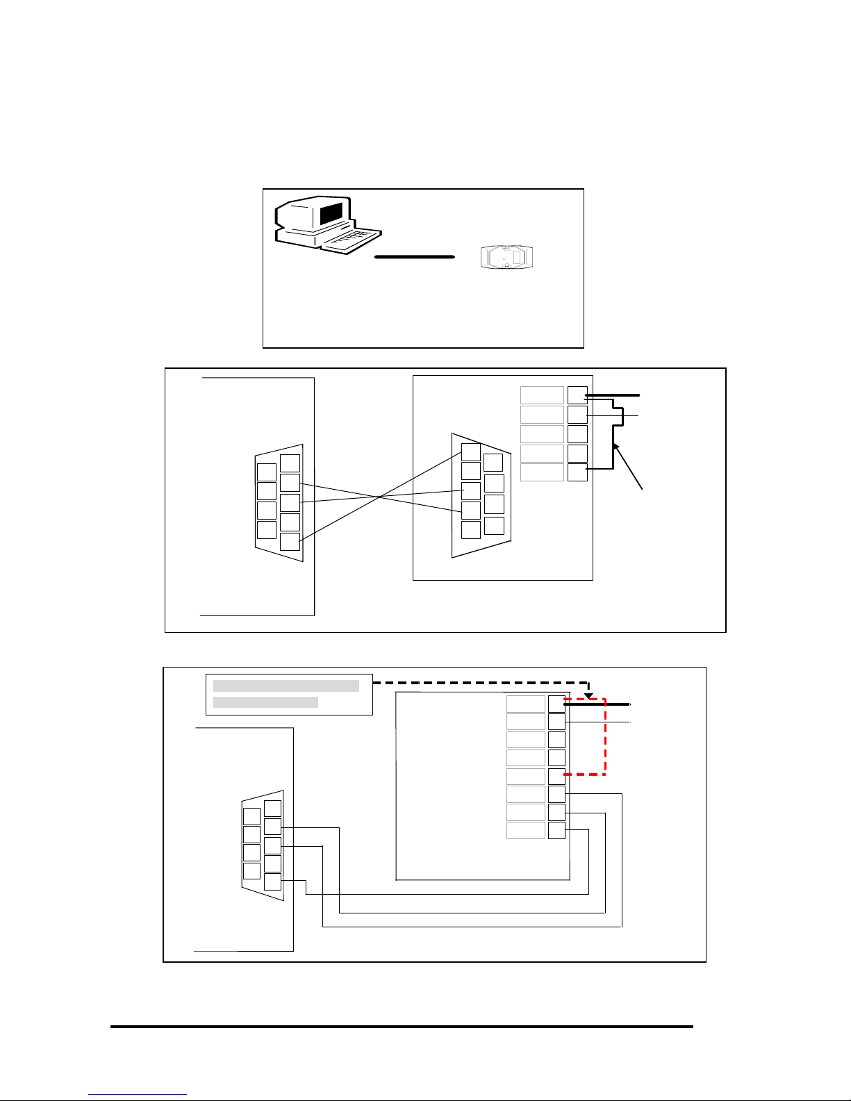
1.6. Wiring Diagrams for Application
1.6.1. Program download
I-7521/I-7522/I-7522A/I-7523A
I-7523/I-7524/I-7527
RS-232
Host PC
RS-232
Signal
I-7521/I-7521D
I-7522/I-7522D
I-7523/I-7523D
12
13
GND
+VS 6 7
8 9 1
2
3
4
5
Male 9-pin D-sub
Com 1/2/3/4 or
UART port
Host PC
Ext. GND
Ext. 24V
9
8
7
6
5 4 3
2
1
Male 9-pin D-sub
COM1
D2-
D2+
INIT*
11
10
9
Connect INIT* pin with
GND pin to disable
autoexec.bat
Download
Cable:CA0910F
11
12
13
14
GND
+VS
D2-
D2+
I-7522A/I-7522AD
I-7523A/I-7523AD
I-7524/I-7524D
I-7527/I-7527D
Ext. GND
Ext. 24V
6 7 8 9 1 2 3 4 5
Male 9-pin D-sub
Com 1/2/3/4 or
UART port
Host PC
RS-232
Signal
7 8 9
10
INIT*
RXD1
TXD1
GND
COM1
RX
TX
GND
Connect INIT* pin with GND pin
to disable autoexec.bat
Download
Cable:CA0910

I-7521/I-7522/I-7522A/I-7523/I-7524/I-7527 User’s Manual,Ver2.5 Aug.2015
26
1.6.2. Using a 3-wire RS-232 port
There are 3 wires as following:
Connect RXD to TXD of RS-232 device
Connect TXD to RXD of RS-232 device
Connect GND to GND of RS-232 device
GND
I-7521/I-7521D
I-7522/I-7522D
I-7523/I-7523D
I-7522A/I-7522AD
I-7524/I-7524D
I-7527/I-7527D
TXD
RXD
RS-232 Device
RI
CTS
RTS
DSR
GND
DTR
TXD
RXD
DCD
I-7521/I-7522/I-7522A/I-7523/I-7524/I-7527 User’s Manual,Ver2.5 Aug.2015
27
1.6.3. Using a 5-wire RS-232 port
There are 5 wires as follows:
Connect RXD to TXD of RS-232 device
Connect TXD to RXD of RS-232 device
Connect RTS to CTS of RS-232 device
Connect CTS to RTS of RS-232 device
Connect GND to GND of RS-232 device
CTS
GND
RTS
I-7521/I-7521D
I-7522/I-7522D
I-7523/I-7523D
I-7522A/I-7522AD
I-7524/I-7524D
I-7527/I-7527D
TXD
RXD
RS-232 Device
RI
CTS
RTS
DSR
GND
DTR
TXD
RXD
DCD
I-7521/I-7522/I-7522A/I-7523/I-7524/I-7527 User’s Manual,Ver2.5 Aug.2015
28
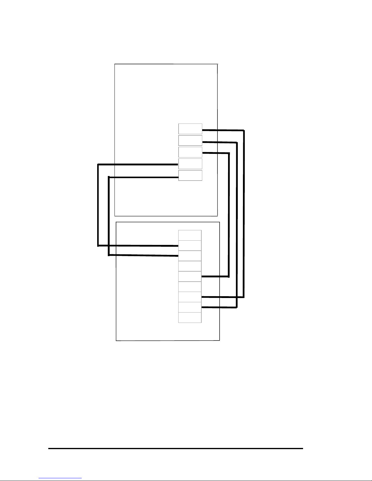
1.6.4. Using a RS-485 port
Note:
The RS-485 interface can directly drive 256 sets of 7000 modules
without a repeater
Ext. GND
Ext. 24V
11
12
13
14
GND
+VS
D2-
D2+
I-7521/I-7521D
I-7522/I-7522D
I-7523/I-7523D
I-7522A/I-7522AD
I-7524/I-7524D
I-7527/I-7527D
Ext. GND
Ext. 24V
7
8 9 10
GND
+VS
D2-
D2+
7000 module
I-7521/I-7522/I-7522A/I-7523/I-7524/I-7527 User’s Manual,Ver2.5 Aug.2015
29
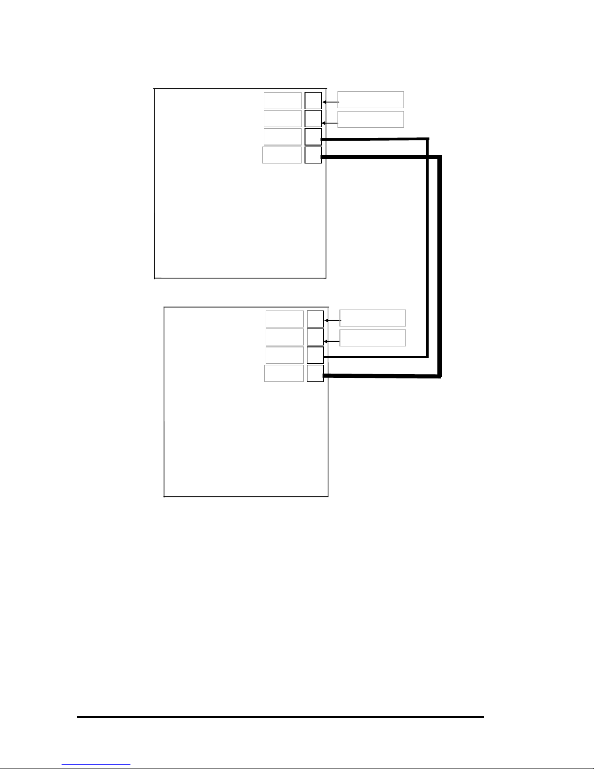
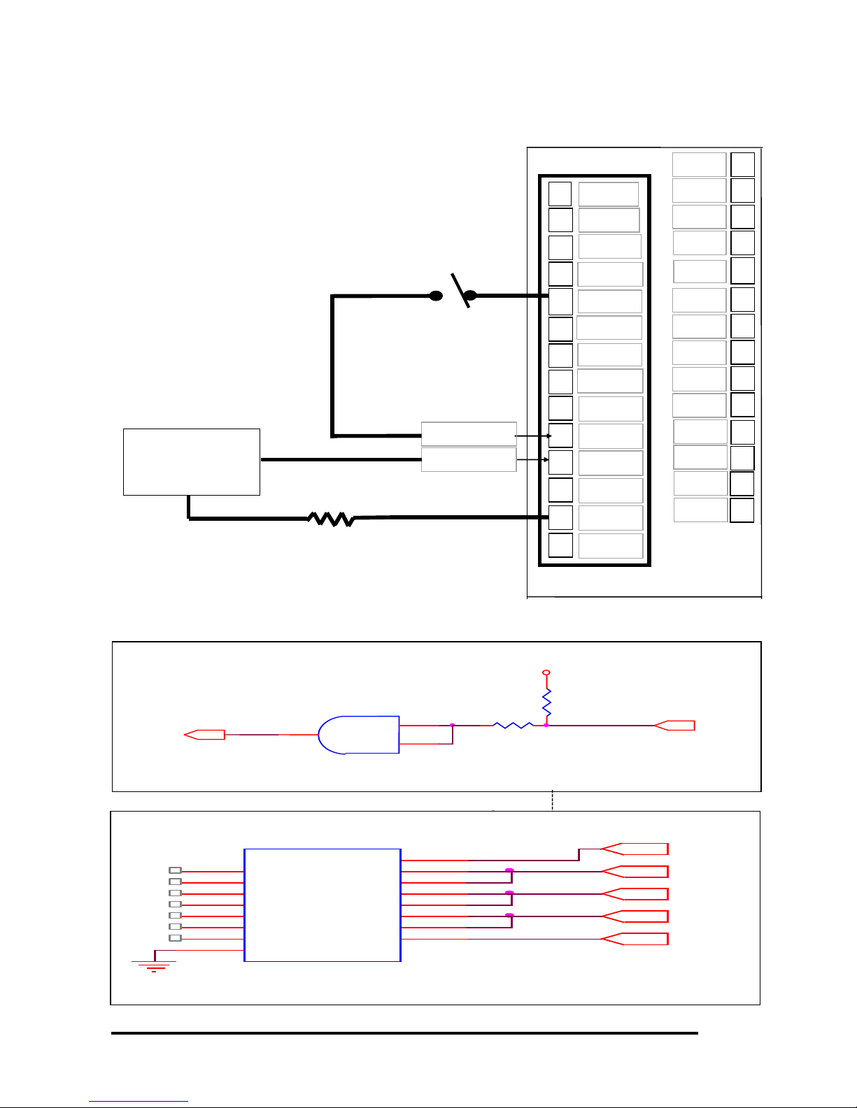
1.6.5. Using DI/DO of I-7521(D)
(valid for I-7521(D)/I-7522(D)/I-7523(D))
Ext. GND
Ext. 24V
10 9 8
7
6
11
5 4 12
13
GND
+VS
D2-
D2+
DO3
DO1
DO2
INIT*
2
1
Data+
TXD
4
5
6 7 8 3 9
RXD
Data-
RTS
I-7521
DI3
DI2
CTS
N/C
GND
N/C
X1
X2
X3
3 2 1
COM1
Dry contact or TTL/CMOS
or (3.5V to 30V D/I)
Inductive load or
Conductive load
Current Limit Resistor
Load current <= 125mA
U?
2003A
1 3 14
2
4
5
6
9
16
15
13
12
11
10
7
8
B0
B2
C2
B1
B3
B4
B5
COM
C0
C1
C3
C4
C5
C6
B6
E
DO1
DO2
DO3
GND
+VS
DIO24
DIO29
DIO30
7521
12
6
5
4
13
+5V
UA
74HCT08
1 2 3
R2
10K
R1
10K
D/I
TO_CPU
7521
D/I Block Diagram
D/O Block Diagram
I-7521/I-7522/I-7522A/I-7523/I-7524/I-7527 User’s Manual,Ver2.5 Aug.2015
30
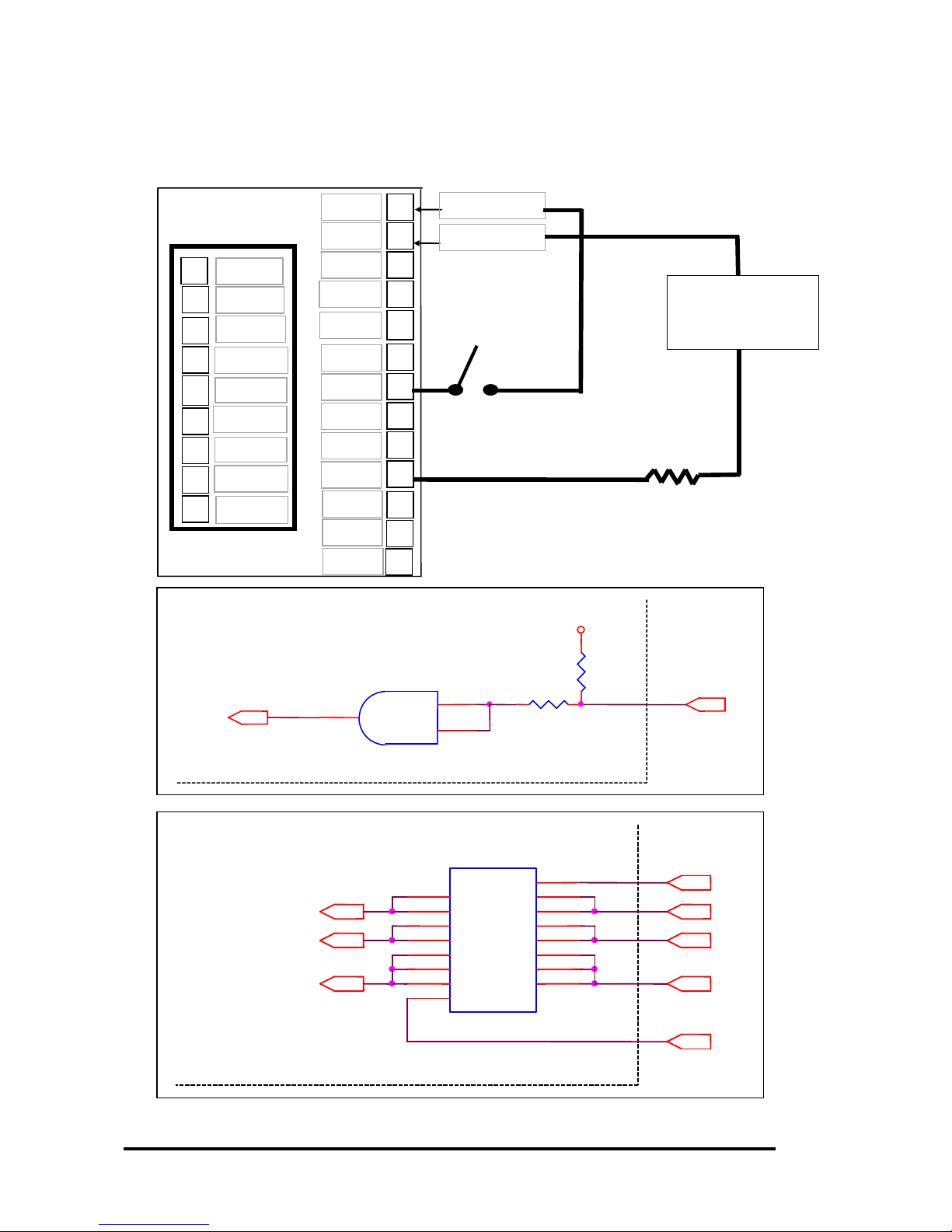
1.6.6. Using DI/DO of I-7522A(D)
(valid for I-7522A(D)/I-7524(D)
/I-7527(D))
Inductive load or
Conductive load
Current Limit Resistor
Load current <= 125mA
Ext. GND
Ext. 24V
Dry contact or TTL/CMOS
or (3.5V to 30V D/I)
11
10
9 8 7
12
6 5 13
14
GND
+VS
D2-
D2+
CTS1
GND
RTS1
INIT*
16
15
TXD3+
TXD3 -
18
19
20
21
22
17
23
RXD3+
GND
DI3
I-7522A
TXD1
RXD1
DI2
DI1
DI0
RXD3 -
D1 -
DI+
DI
4 3 2
X507
24
PWR
25
DO0
26
DO1
270
DO2
28
DO3
DO
1
+5V
UA 74HCT08
1
2 3 R2 10K R1
10K
D/I
TO_CPU
7522A
19~22
+5V
UA
74HCT08
1
2 3 R2
10K
R1
10K
D/I
TO_CPU
7522A
D/I Block Diagram
DO0
DO1
DO2
DO3
PWR
U1
ULN2003A
SOIC 16
1
2
3
4
5
6
7
8
9
10
11
12
13
14
15
16
B0
B1
B2
B3
B4
B5
B6
E
COM
C6
C5
C4
C3
C2
C1
C0
D/O Block Diagram
24
25
26
27
28
 Loading...