


I-7021/22/24, M-7022/24/28 User Manual, Rev: B2.3
1
I-7021, I-7022, I-7024, M-7022,
M-7024 and M-7028 Series
User Manual
Warranty
All products manufactured by ICP DAS are under
warranty regarding defective materials for a period of one
year from the date of delivery to the original purchaser.
Warning
ICP DAS assumes no liability for damages resulting
from the use of this product. ICP DAS reserves the right
to change this manual at any time without notification.
The information furnished by ICP DAS is believed to be
accurate and reliable. However, no responsibility is
assumed by ICP DAS for its use, or for any infringements
of patents or other rights of third parties resulting from its
use.
Copyright
Copyright 1999 - 2009 ICP DAS. All rights reserved.
Trademark
The names used for identification only may be
registered trademarks of their respective companies.
Date: 2016/03/16

I-7021/22/24, M-7022/24/28 User Manual, Rev: B2.3
2
Table of Contents
1. Introduction ............................................................................................... 6
1.1 More Information ............................................................... 8
1.2 Terminal Assignment ......................................................... 9
1.3 Specifications ................................................................... 12
1.4 Block Diagrams ................................................................ 15
1.4.1 Block Diagram for the I-7021 and I-7021P ............ 15
1.4.2 Block Diagram for the I-7022 and M-7022 ............ 15
1.4.3 Block Diagram for the I-7024, M-7024 and M-
7024L ............................................................................... 16
1.4.4 Block Diagram for the I-7024R and M-7024R ...... 16
1.4.5 Block Diagram for the M-7024U ........................... 17
1.4.6 Block Diagram for the M-7028 .............................. 17
1.5 Dimensions ....................................................................... 18
1.5.1 Modules without Frame Ground ............................. 18
1.5.2 Modules with Frame Ground .................................. 19
1.6 Jumper Settings ................................................................ 20
1.6.1 I-7021and I-7021P Jumper Settings ....................... 20
1.6.2 I-7022 and M-7022 Jumper Settings ...................... 21
1.7 Wiring .............................................................................. 22
1.7.1 Wiring diagram for the I-7021, I-7021P, I-7022 and
M-7022 ............................................................................. 22
1.7.2 Wiring diagram for the I-7024, I-7024R, M-7024,
M-7024L and M-7024R ................................................... 22
1.7.3 Wiring diagram for the M-7024U........................... 23
1.7.4 Wiring diagram for the M-7028 ............................. 23
1.7.5 Wiring Recommendations ...................................... 23
1.8 Quick Start ....................................................................... 24
1.9 Default Settings ................................................................ 26
1.10 Calibration ...................................................................... 27
1.11 Configuration Tables ..................................................... 35
1.12 M-7000 Notes ................................................................ 41
1.12.1 Protocol Switching ................................................ 41
1.12.2 INIT Mode ............................................................ 42
1.13 Mounting ........................................................................ 43
1.13.1 Din-Rail Mounting ................................................ 43

I-7021/22/24, M-7022/24/28 User Manual, Rev: B2.3
3
1.13.2 Piggyback Mounting ............................................. 45
1.13.3 Wall Mounting ...................................................... 46
1.14 Technical Support .......................................................... 47
2. DCON Protocol ....................................................................................... 48
2.1 %AANNTTCCFF ............................................................ 54
2.2 #AA(Data) ........................................................................ 57
2.3 #AAN ............................................................................... 59
2.4 #AAN(Data) ..................................................................... 61
2.5 $AA0 ................................................................................ 64
2.6 $AA0N ............................................................................. 66
2.7 $AA1 ................................................................................ 68
2.8 $AA1N ............................................................................. 70
2.9 $AA2 ................................................................................ 72
2.10 $AA3VV ........................................................................ 74
2.11 $AA3NVV ..................................................................... 76
2.12 $AA4 .............................................................................. 78
2.13 $AA4N ........................................................................... 80
2.14 $AA5 .............................................................................. 82
2.15 $AA6 .............................................................................. 84
2.16 $AA6 .............................................................................. 86
2.17 $AA6N ........................................................................... 88
2.18 $AA7 .............................................................................. 90
2.19 $AA7N ........................................................................... 92
2.20 $AA7N ........................................................................... 94
2.21 $AA8 .............................................................................. 96
2.22 $AA8N ........................................................................... 98
2.23 $AA9N ......................................................................... 100
2.24 $AA9NTS .................................................................... 102
2.25 $AAB ........................................................................... 104
2.26 $AACN ........................................................................ 106
2.27 $AAF ............................................................................ 108
2.28 $AAI ............................................................................. 109
2.29 $AAM .......................................................................... 111
2.30 $AAP ............................................................................ 112
2.31 $AAPN ......................................................................... 114
2.32 $AAS1 .......................................................................... 116
2.33 ~AAO(Name) ............................................................... 118
2.34 ~** ................................................................................ 120

I-7021/22/24, M-7022/24/28 User Manual, Rev: B2.3
4
2.35 ~AA0 ............................................................................ 121
2.36 ~AA1 ............................................................................ 123
2.37 ~AA2 ............................................................................ 125
2.38 ~AA3EVV .................................................................... 127
2.39 ~AA4 ............................................................................ 129
2.40 ~AA4 ............................................................................ 131
2.41 ~AA4N ......................................................................... 133
2.42 ~AA5 ............................................................................ 135
2.43 ~AA5N ......................................................................... 137
2.44 ~AA5PPSS ................................................................... 139
2.45 @AABB ....................................................................... 141
2.46 @AABBHH ................................................................. 143
2.47 @AACECN .................................................................. 145
2.48 @AADI ........................................................................ 147
2.49 @AADODD ................................................................. 149
2.50 @AARECN .................................................................. 151
3. Modbus RTU Protocol .......................................................................... 153
3.1 01 (0x01) Read Coils ..................................................... 154
3.2 02 (0x02) Read Discrete Inputs ..................................... 155
3.3 03 (0x03) Read Output Channels .................................. 156
3.4 04 (0x04) Read Input Channels ..................................... 157
3.5 05 (0x05) Write Single Coil ........................................... 158
3.6 06 (0x06) Write Single Register .................................... 159
3.7 15 (0x0F) Write Multiple Coils ..................................... 160
3.8 16 (0x10) Write Multiple Registers ............................... 161
3.9 M-7022 Address Mappings ........................................... 162
3.10 M-7024/M-7024L Address Mappings ......................... 164
3.11 M-7024R Address Mappings ....................................... 166
3.12 M-7024U Address Mappings....................................... 169
3.13 M-7028 Address Mappings ......................................... 173
4. Troubleshooting .................................................................................... 175
4.1 Communicating with the module ................................... 176
A. Appendix .............................................................................................. 177
A.1 INIT Mode .................................................................... 177
A.2 Dual Watchdog Operation ............................................ 179
A.3 Module Output Status ................................................... 180
A.4 Reset Status ................................................................... 181
A.5 Analog Output ............................................................... 182

I-7021/22/24, M-7022/24/28 User Manual, Rev: B2.3
5
A.6 Slew Rate Control ......................................................... 184
A.7 Analog Output Read-back ............................................. 185
A.8 Frame Ground ............................................................... 186
I-7021/22/24, M-7022/24/28 User Manual, Rev: B2.3
6
1. Introduction
The I-7000 series is a family of network data acquisition
and control modules, providing analog-to-digital, digitalto-analog, digital input/output, timer/counter and other
functions. The modules can be remotely controlled using a
set of commands, which we call the DCON protocol.
Communication between the module and the host is in
ASCII format via an RS-485 bi-directional serial bus
standard. Baud Rates are software programmable and
transmission speeds of up to 115.2 Kbps can be selected.
The functionality of the M-7000 series is the same as the
I-7000 series, with the exception that the M-7000 series
offers extended support for the Modbus RTU protocol.
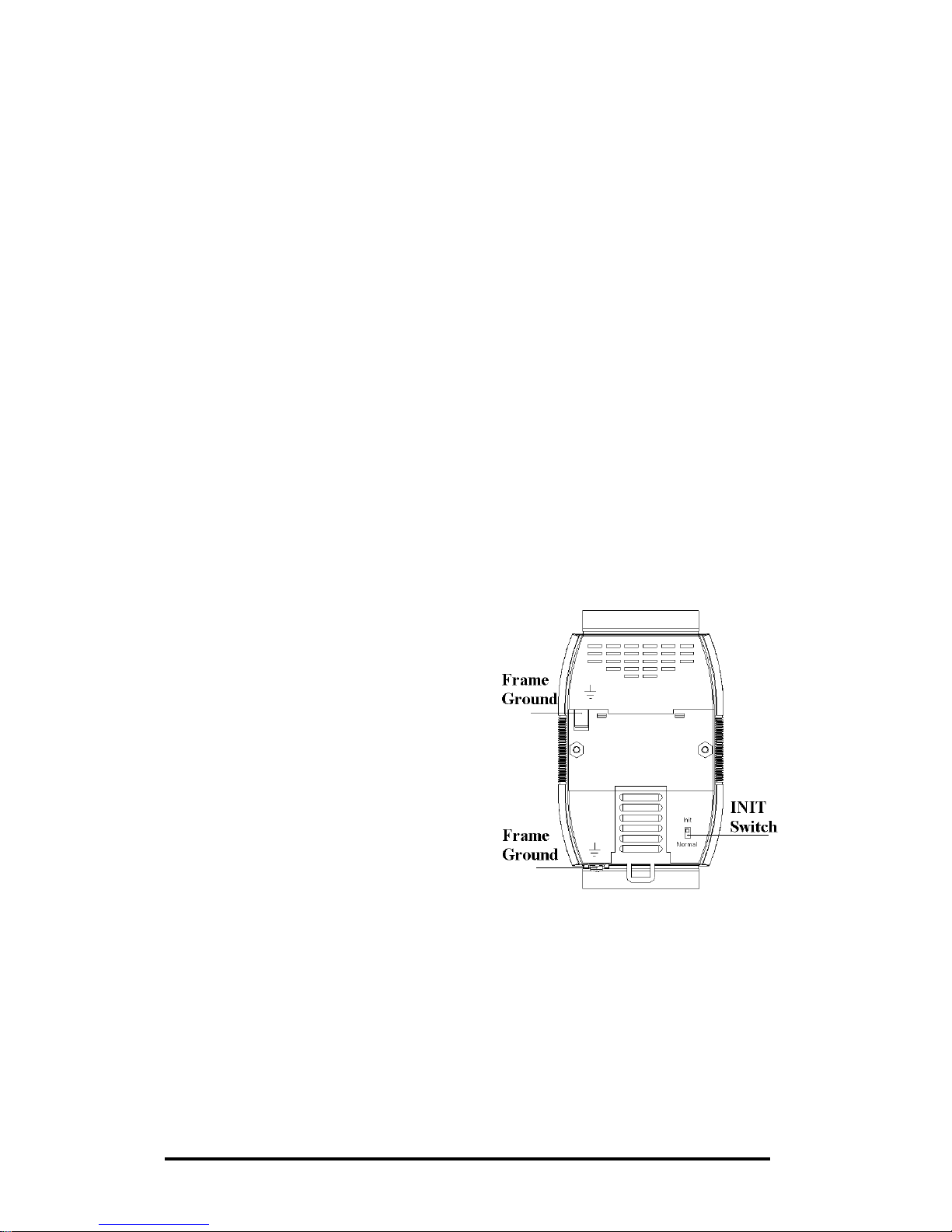
Some I-7000 modules feature
a new design for the frame
ground and INIT switch as
shown in the figure (rear
view). The frame ground
provides enhanced static
protection (ESD) abilities and
ensures the module is more
reliable. The INIT switch
allows easier access to INIT
mode. Please refer to Sections
A.1 and A.3 for more details.
The common features of the I-7021/21P, I-7022, I-7024,
I-7024R, M-7022, M-7024, M-7024L, M-7024R,
M-7024U and M-7028 modules are as follows:

I-7021/22/24, M-7022/24/28 User Manual, Rev: B2.3
7
1. 3000VDC, 2500VDC for M-7024U, inter-module
isolation
2. Programmable power-on value for analog output
3. Programmable slew rate
4. Software calibration
The I-7021 is a single channel analog output module with
12-bit resolution and output read-back function. The
I-7021P is similar to the I-7021 but with 16-bit resolution.
The I-7022/M-7022 is a 2-channel analog output module
with 12-bit resolution and output read-back function. The
I-7024/M-7024 is a 4-channel analog output module with
14-bit resolution and supports bipolar voltage output. The
M-7024L is a 4-channel analog output module with 12-bit
resolution and supports bipolar voltage output. The
I-7024R/M-7024R is I-7024/M-7024 added 5-channel
digital inputs. The M-7024U is a 4-channel analog output
module with 16-bit resolution and supports bipolar voltage
output. There is also 4-channel digital inputs and
4-channel digital outputs for the M-7024U. The M-7028
is a 8-channel analog output module with 12-bit resolution.

I-7021/22/24, M-7022/24/28 User Manual, Rev: B2.3
8
1.1 More Information
For more information regarding the I-7000 series, please
refer to chapter 1 of the “I-7000 Bus Converter User’s
Manual” as shown below or visit the ICP DAS website
http://www.icpdas.com.
1.1 The 7000 Series Overview
1.2 Related Documentation for the 7000 Series
1.3 Common Features of the 7000 Series
1.4 The 7000 Series System Network Configuration
1.5 7000 Dimensions
I-7021/22/24, M-7022/24/28 User Manual, Rev: B2.3
9
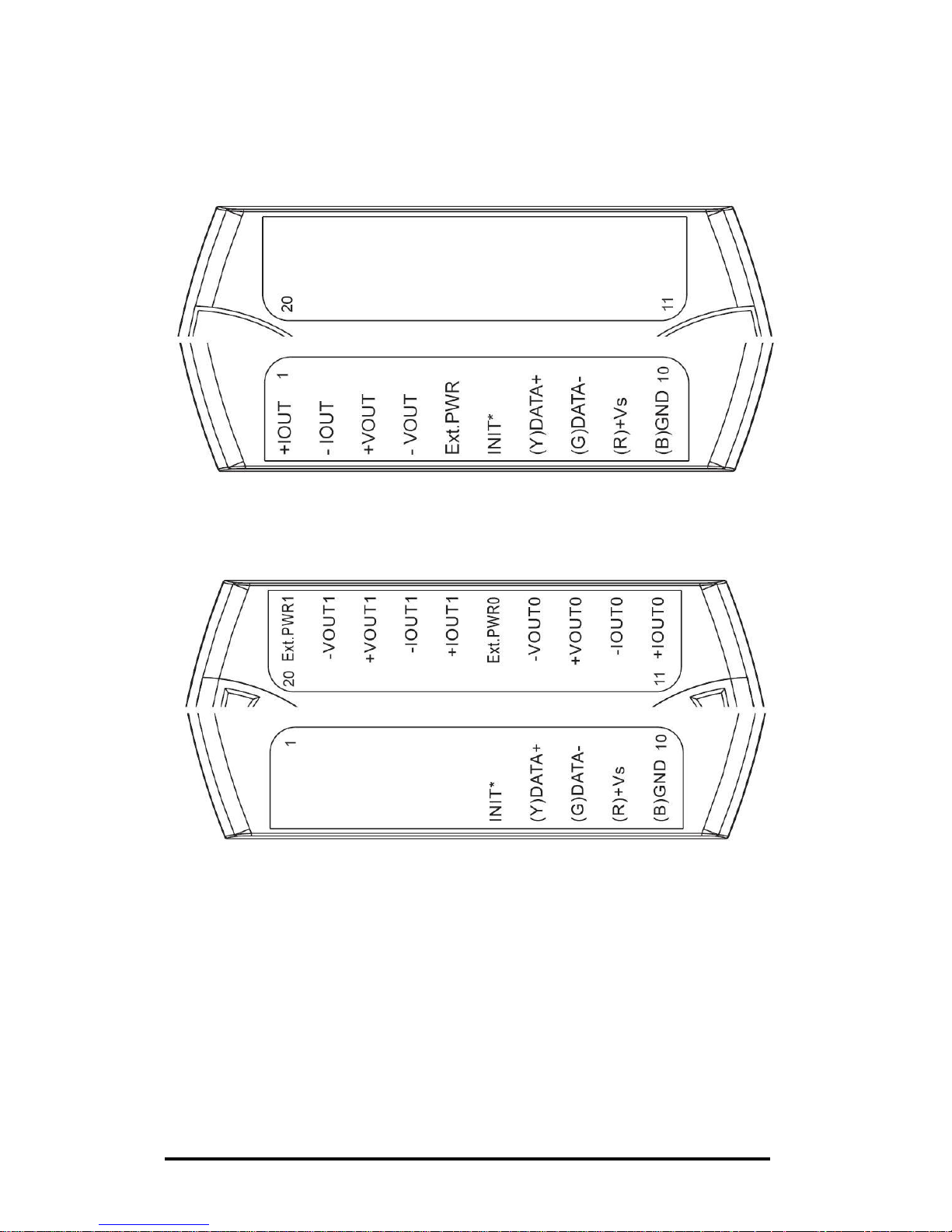
1.2 Terminal Assignment
7021/7021P
7022
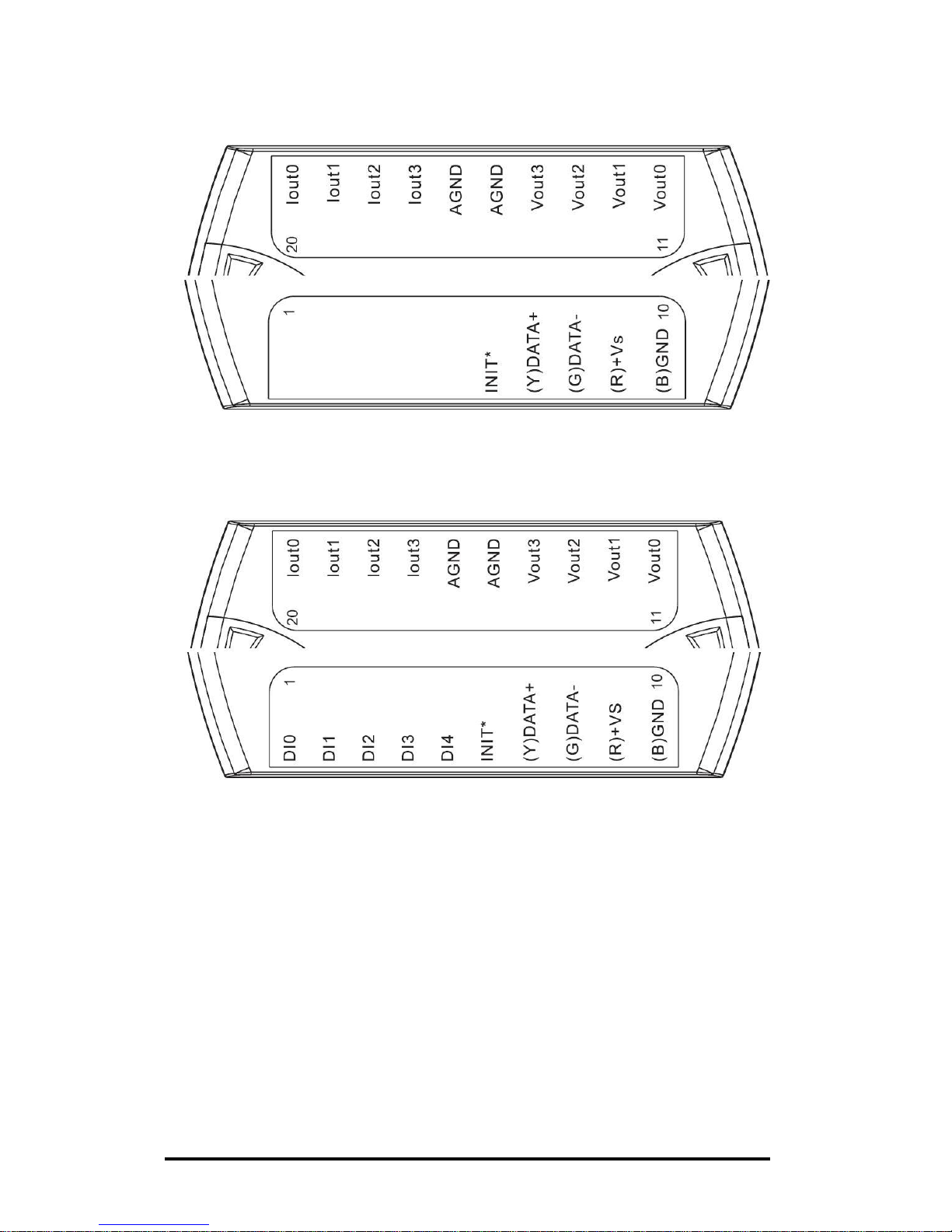
I-7021/22/24, M-7022/24/28 User Manual, Rev: B2.3
10
7024/7024L
7024R
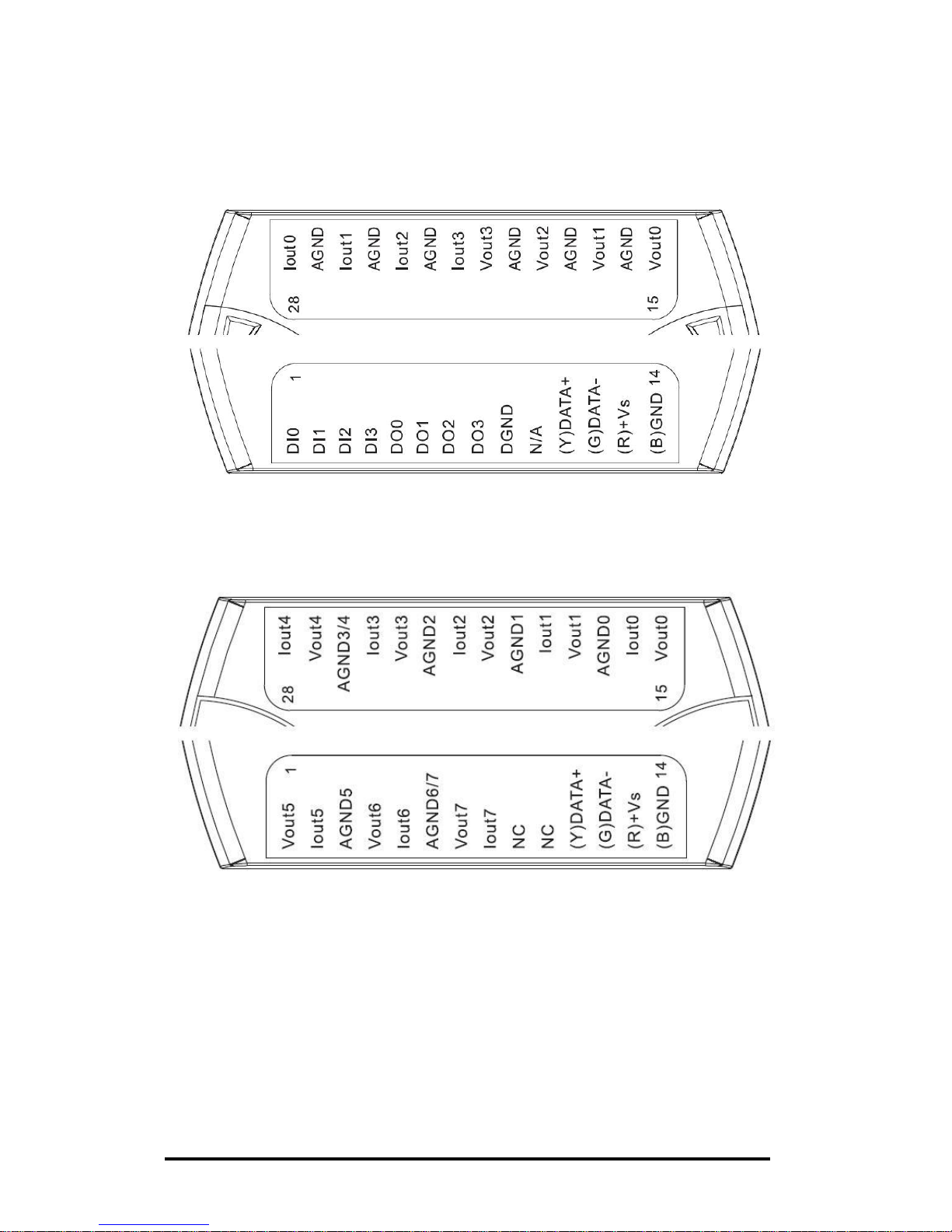
I-7021/22/24, M-7022/24/28 User Manual, Rev: B2.3
11
7024U
7028

I-7021/22/24, M-7022/24/28 User Manual, Rev: B2.3
12
1.3 Specifications
I-7021/I-7021P
I-7022/M-7022
I-7024/M-7024/
M-7024L
Analog Output
Output Channels
1 2 4
Output Type
mA, V
mA, V
mA, V
Accuracy
±0.1% for I-7021
±0.02% for I-7021P
±0.1% of FSR
±0.1% of FSR
Resolution
12-bit for I-7021
16-bit for I-7021P
12-bit
14-bit for I-7024 and
M-7024
12-bit for M-7024L
Read-back
Accuracy
±1% of FSR
±1% of FSR
NA
Programmable
Output Slope
0.125 ~ 1024 mA/s
0.0625 ~ 512 V/s
0.125 ~ 1024 mA/s
0.0625 ~ 512 V/s
0.125 ~ 2048 mA/s
0.0625 ~ 1024 V/s
Current Load
Resistance
Int. power: 500 ohm
Ext. 24 V: 1050 ohm
Int. power: 500 ohm
Ext. 24 V: 1050 ohm
Ext. 24 V: 1050 ohm
Isolation
3000 VDC
3000 VDC
3000 VDC
Modbus RTU
M-7022
M-7024/M-7024L
Power
Requirements
+10 to +30 VDC
+10 to +30 VDC
+10 to +30 VDC
Consumption
1.8 W
3.0 W
2.4 W (I-7024/M-7024)
2.7 W (M-7024L)
Temperature
Range
Operating
-25°C to +75°C
-25°C to +75°C
-25°C to +75°C
Storage
-40°C to +85°C
-40°C to +85°C
-40°C to +85°C
Notes:
1. A warm up period of 30 minutes is recommended in order to achieve the complete
performance results described in the specifications.
2. The specifications are typical at 25°C unless otherwise stated.
I-7021/22/24, M-7022/24/28 User Manual, Rev: B2.3
13
I-7024R
M-7024R
M-7024U
Analog Output
Output Channels
4 4 4
Output Type
mA, V
mA, V
mA, V
Accuracy
±0.1% of FSR
±0.1% of FSR
±0.02% of FSR
Resolution
14-bit
14-bit
16-bit
Read-back
Accuracy
NA
NA
NA
Programmable
Output Slope
0.125 ~ 2048 mA/s
0.0625 ~ 1024 V/s
0.125 ~ 2048 mA/s
0.0625 ~ 1024 V/s
0.125 ~ 1024 mA/s
0.0625 ~ 512 V/s
Current Load
Resistance
Ext. 24 V: 1050 ohm
Ext. 24 V: 1050 ohm
Int. power: 1000 ohm
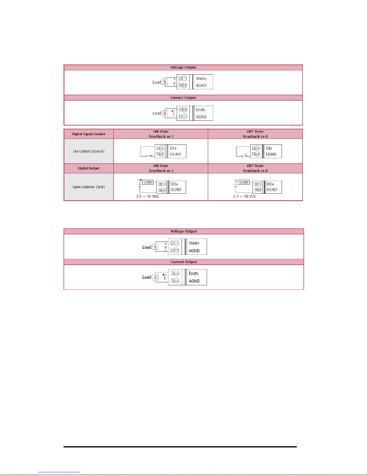
Digital Input
Channels
5 5 4
Input Type
Dry Contact (Source)
Dry Contact (Source)
Dry Contact (Source)
Contact Level
On: Close to GND
Off: Open
On: Close to GND
Off: Open
On: Close to GND
Off: Open
Counters
16-bit
16-bit
16-bit
Min. Pulse Width:
10ms
Min. Pulse Width:
10ms
Min. Pulse Width: 5ms
Digital Output
Channels
4
Output Type
Open Collector
Sink/Source
Sink
Load Voltage
+3.5 VDC ~ +50 VDC
Max. Load
Current
700 mA/Channel
Isolation
3000 VDC
3000 VDC
2500 VDC
Modbus RTU
No
Yes
Yes
Power
Requirements
+10 to +30 VDC
+10 to +30 VDC
+10 to +30 VDC
Consumption
3.2 W
3.2 W
4.5 W
Temperature
Range
Operating
-25°C to +75°C
-25°C to +75°C
-25°C to +75°C
Storage
-40°C to +85°C
-40°C to +85°C
-40°C to +85°C
Notes:
1. A warm up period of 30 minutes is recommended in order to achieve the complete
performance results described in the specifications.
2. The specifications are typical at 25°C unless otherwise stated.
I-7021/22/24, M-7022/24/28 User Manual, Rev: B2.3
14
M-7028
Analog Output
Output Channels
8
Output Type
mA, V
Accuracy
±0.1% of FSR
Resolution
12-bit
Read-back
Accuracy
NA
Programmable
Output Slope
0.125 ~ 1024 mA/s
0.0625 ~ 512 V/s
Current Load
Resistance
500 ohm
Isolation
3000 VDC
Modbus RTU
Yes
Power
Requirements
+10 to +30 VDC
Consumption
4.3 W
Temperature
Range
Operating
-25°C to +75°C
Storage
-40°C to +85°C
Notes:
1. A warm up period of 30 minutes is recommended in order to achieve the complete
performance results described in the specifications.
2. The specifications are typical at 25°C unless otherwise stated.
I-7021/22/24, M-7022/24/28 User Manual, Rev: B2.3
15
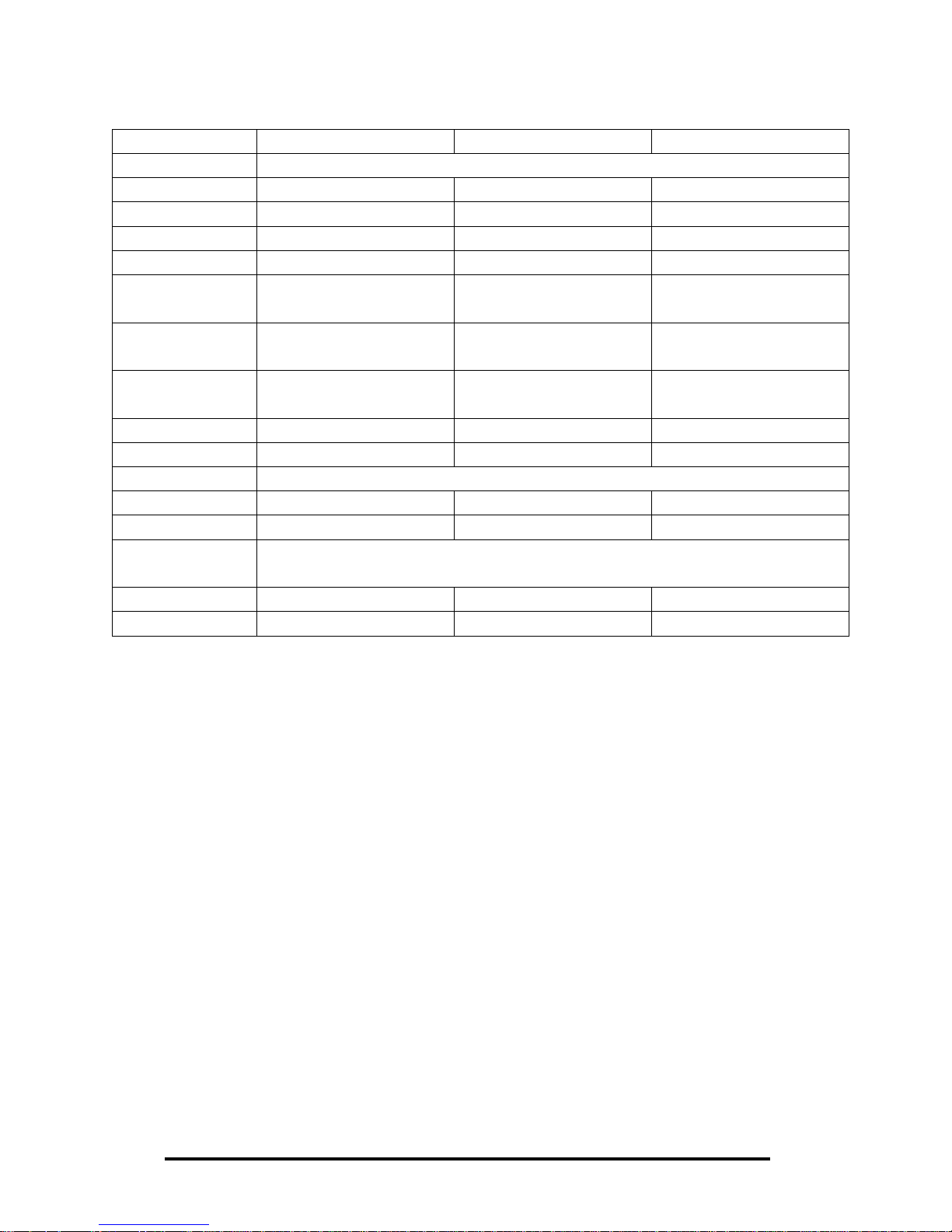
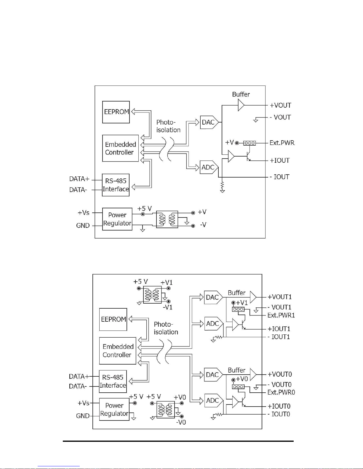
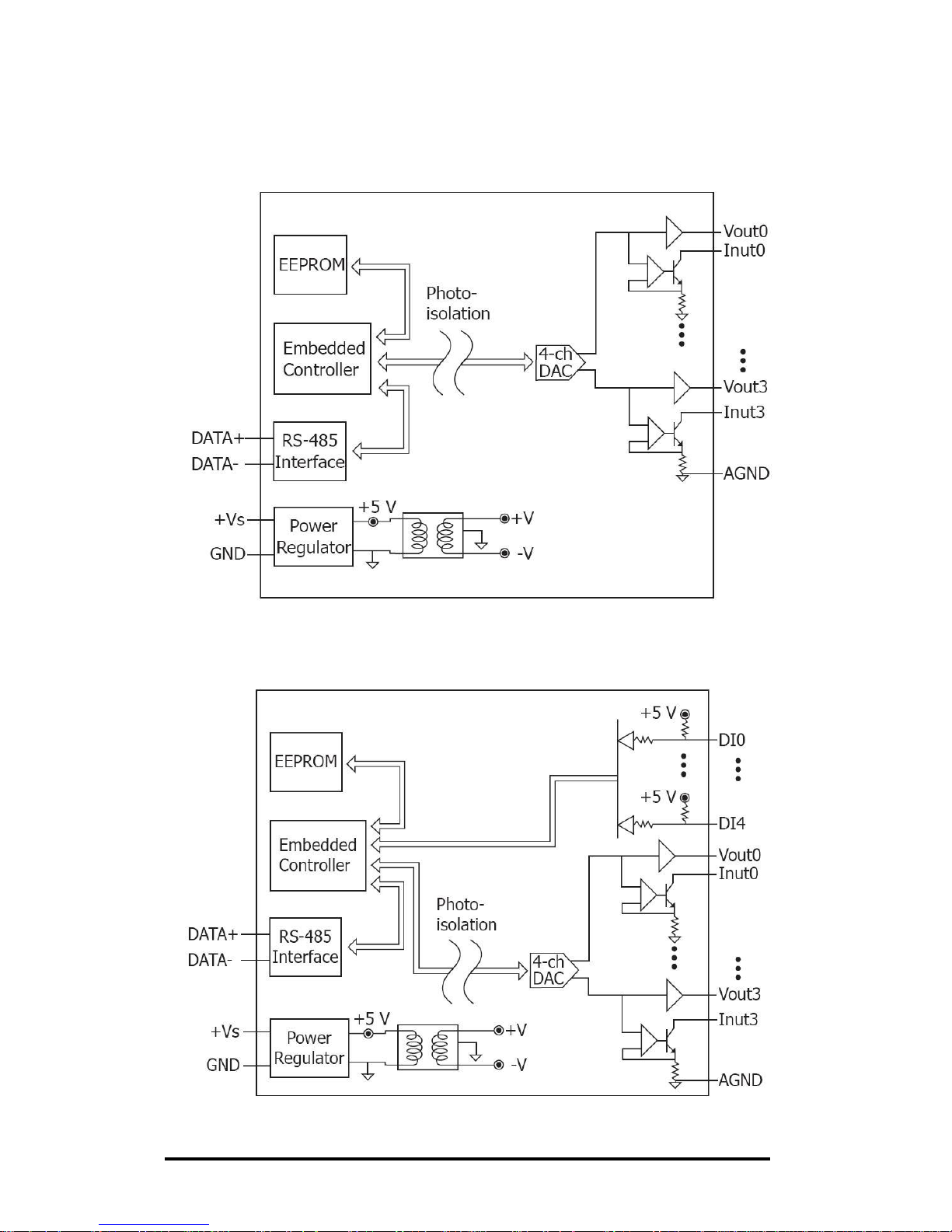
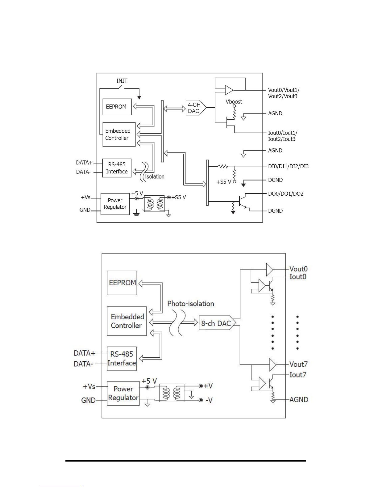
1.4 Block Diagrams
1.4.1 Block Diagram for the I-7021 and I-7021P
1.4.2 Block Diagram for the I-7022 and M-7022
I-7021/22/24, M-7022/24/28 User Manual, Rev: B2.3
16
1.4.3 Block Diagram for the I-7024, M-7024 and
M-7024L
1.4.4 Block Diagram for the I-7024R and M-7024R
I-7021/22/24, M-7022/24/28 User Manual, Rev: B2.3
17
1.4.5 Block Diagram for the M-7024U
1.4.6 Block Diagram for the M-7028
I-7021/22/24, M-7022/24/28 User Manual, Rev: B2.3
18
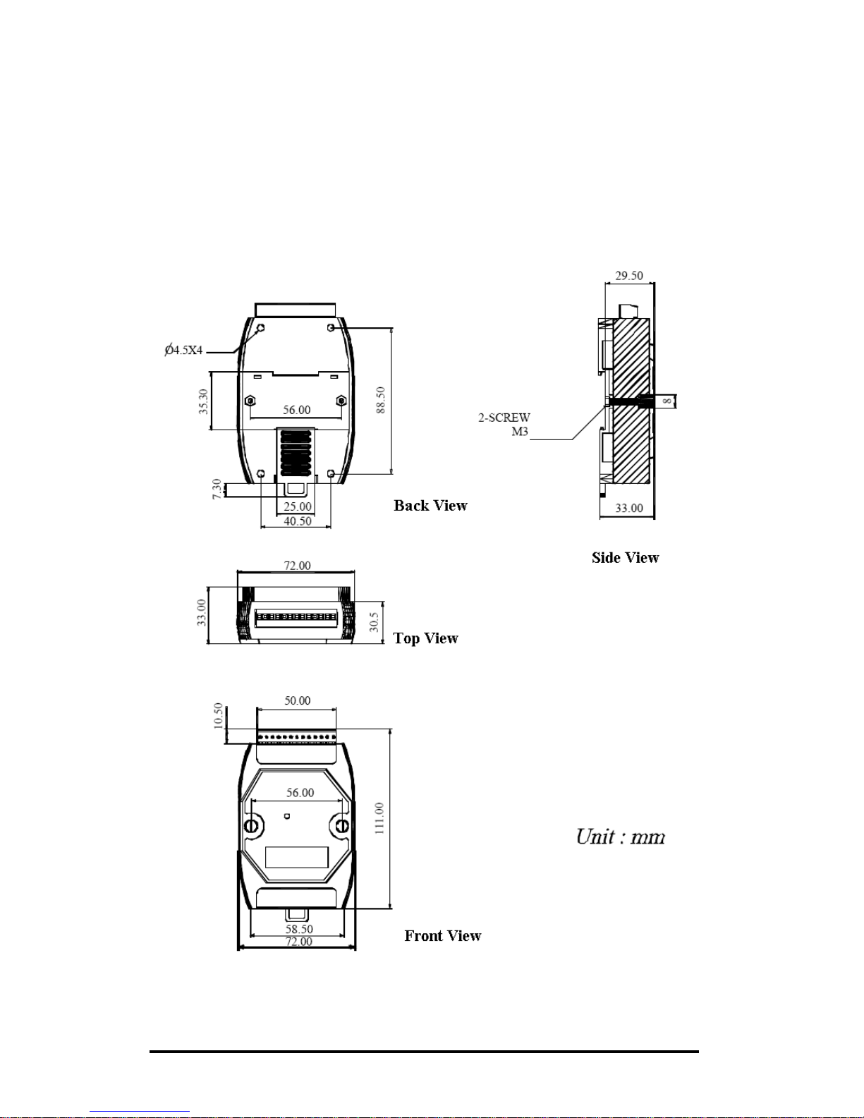
1.5 Dimensions
1.5.1 Modules without Frame Ground
The dimensions of the I-7021, I-7021P, I-7022, and
M-7022 are as shown below.
I-7021/22/24, M-7022/24/28 User Manual, Rev: B2.3
19
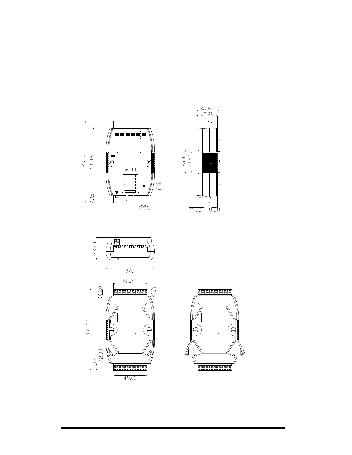
1.5.2 Modules with Frame Ground
The dimensions of the I-7024, M-7024, M-7024L,
I-7024R, M-7024R, M-7024U and M-7028 are as shown
below.
Back View
Top View
Front View
Side View
Unit : mm
lnit
Normal
I-7021/22/24, M-7022/24/28 User Manual, Rev: B2.3
20
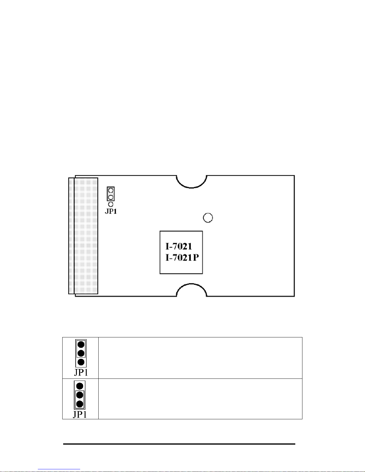
1.6 Jumper Settings
Note: To access the jumpers, the cover must be opened.
1.6.1 I-7021and I-7021P Jumper Settings
For the I-7021 and I-7021P modules, the power supply for
current output can be either internal or external. The
power supply is selected using the JP1 jumper. The
position of the JP1 jumper is shown in the figure below.
The settings for the JP1 jumper are as follows.
Select internal power. It can drive load up to 500
ohm. (factory default)
Select external power. It can drive load up to
1050 ohm for 24 V external power supply.

I-7021/22/24, M-7022/24/28 User Manual, Rev: B2.3
21
1.6.2 I-7022 and M-7022 Jumper Settings
For the I-7022 and M-7022 modules, the power supply for
current output can be either internal or external. The
power supply is selected using the JP1 jumper for channel
0 and JP2 for channel 1. The positions of the JP1 and JP2
jumpers are shown in the figure below.
The settings for the JP1 and JP2 jumpers are as follows.
Select internal power. It can drive load up to 500
ohm. (factory default)
Select external power. It can drive load up to
1050 ohm for 24 V external power supply.
I-7021/22/24, M-7022/24/28 User Manual, Rev: B2.3
22
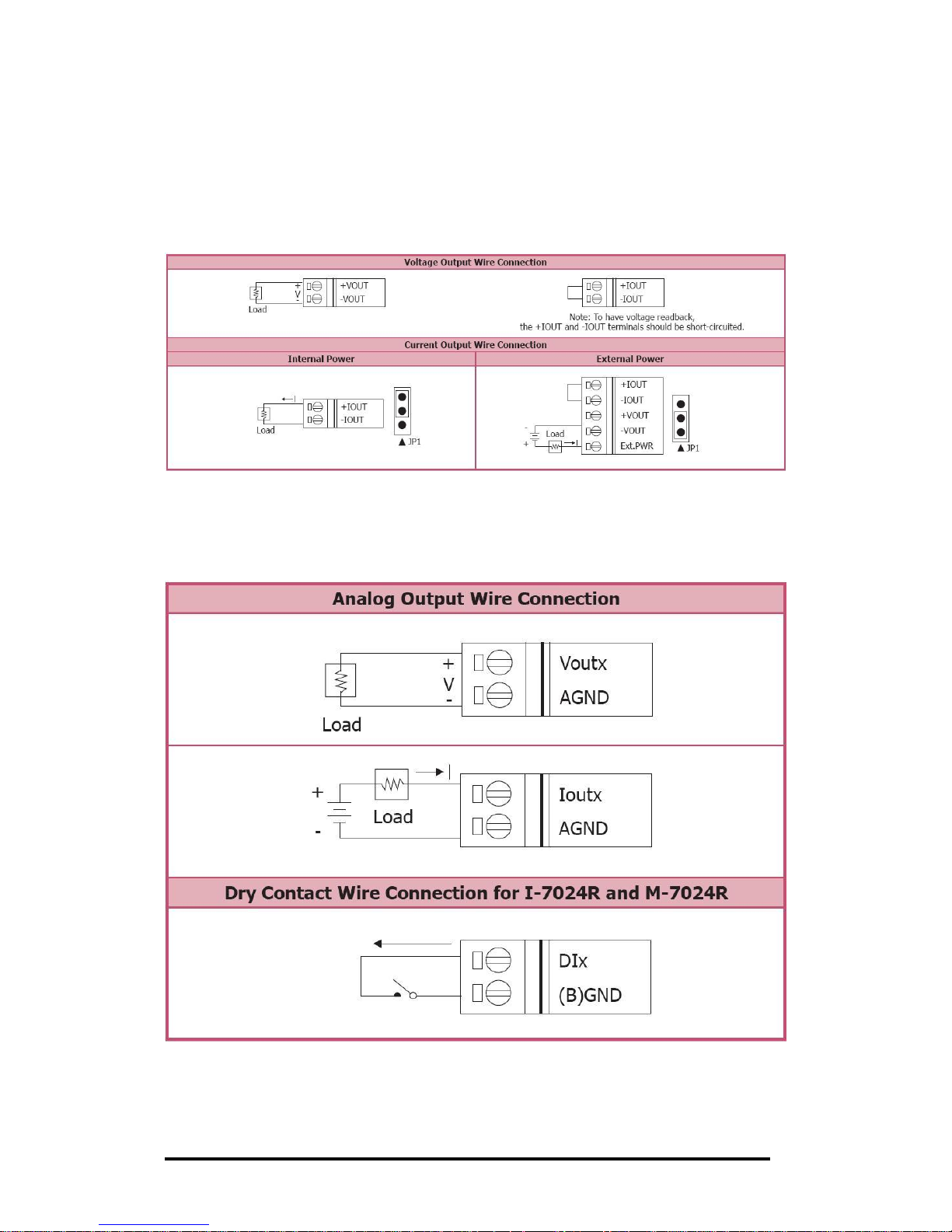
1.7 Wiring
1.7.1 Wiring diagram for the I-7021, I-7021P,
I-7022 and M-7022
1.7.2 Wiring diagram for the I-7024, I-7024R,
M-7024, M-7024L and M-7024R
I-7021/22/24, M-7022/24/28 User Manual, Rev: B2.3
23
1.7.3 Wiring diagram for the M-7024U
1.7.4 Wiring diagram for the M-7028
1.7.5 Wiring Recommendations
Use 26-12 AWG wire for signal connections.
Strip the wire to a length of 7±0.5 mm.
Use a crimp terminal for wiring.
Avoid high-voltage cables and power equipment as
much as possible.
For RS-485 communication, use insulated and
twisted pair 24 AWG wire, e.g. Belden 9841.

I-7021/22/24, M-7022/24/28 User Manual, Rev: B2.3
24
1.8 Quick Start
To install the module, follow the steps below:
1. For current output, adjust the jumper setting for the
I-7021/21P, I-7022 and M-7022. See Section 1.6 for
the jumper settings.
2. Connect the output load. See Section 1.2 for the
terminal assignment and Section 1.7 for the wiring
diagram.
3. Connect the module to the RS-485 network using the
DATA+ and DATA- terminals. See Section 1.2 for the
terminal assignment. If the host is only equipped with
an RS-232 interface, then an RS-232 to RS-485
converter will be required. Refer to the “I-7000 Bus
Converter User’s Manual” for more information.
4. Connect the module to the power supply using the +Vs
and GND terminals. See Section 1.2 for the terminal
assignment. Note that the voltage supplied to the
module should be in the range of +10 to +30 VDC.
5. For I-7000 modules, configure the module by sending
the %AANNTTCCFF command. See Section 2.1 for
details. To configure the I-7022, the $AA9NTS
command must also be sent. See Section 2.24 for
details. For M-7000 modules using the Modbus RTU
protocol, configure the module using the following
Modbus registers: 40485, 40486, and 40487. The
Modbus registers started at 40257 are required for
configuring M-7022, M-7024U and M-7028. The
default settings for the module can be found in Section
1.9.
6. For I-7000 modules, in order to write data to the analog
output channels, send the #AA(data) or #AAN(data)
commands to the module. See Sections 2.2 and 2.4 for
details. For M-7000 modules using the Modbus RTU

I-7021/22/24, M-7022/24/28 User Manual, Rev: B2.3
25
protocol, use Functions 06h or 10h to write the data to
the analog output channels. See Section 3.6 and 3.8 for
details.
7. If the host is a PC with a Windows operating system
installed, the DCON Utility can be used to allow easy
configuration and reading of data. The DCON Utility
can be downloaded from the ICP DAS website
(http://www.icpdas.com). The documentation for the
DCON Utility can be found in the ”Getting Started
For I-7000 Series Modules” manual.
Please refer to the “I-7000 Bus Converter User’s
Manual” and ”Getting Started For I-7000 Series
Modules” manuals for more details. The “Getting
Started for I-7000 Series Modules” manual can be
downloaded from the ICP DAS website
(http://www.icpdas.com).

I-7021/22/24, M-7022/24/28 User Manual, Rev: B2.3
26
1.9 Default Settings
Default settings for the I-7021/21P, I-7022, I-7024 and
I-7024R modules are as follows:
▫ Module address: 01
▫ Analog output type: 0 ~ +10 V
▫ Baud rate: 9600 bps
▫ Checksum disabled
▫ Engineering unit format
▫ I-7021/21P and I-7022 jumper setting: internal power
Default settings for the M-7022, M-7024, M-7024L,
M-7024R, M-7024U and M-7028 modules are as follows:
▫ Protocol: Modbus RTU
▫ Module address: 01
▫ Analog output type: 0 ~ +10 V
▫ Baud Rate: 9600 bps
▫ Engineering unit format
▫ M-7022 jumper setting: internal power
I-7021/22/24, M-7022/24/28 User Manual, Rev: B2.3
27
1.10 Calibration
Warning: It is not recommended that calibration be
performed until the process is fully understood.
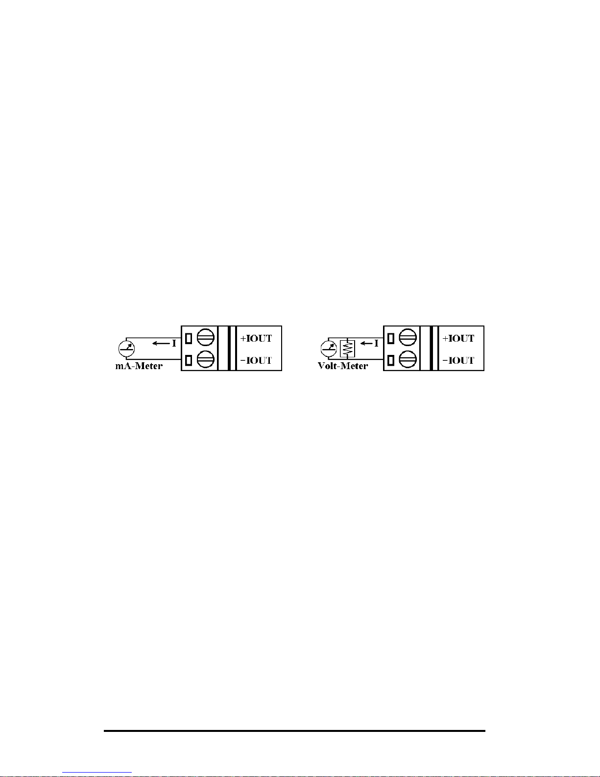
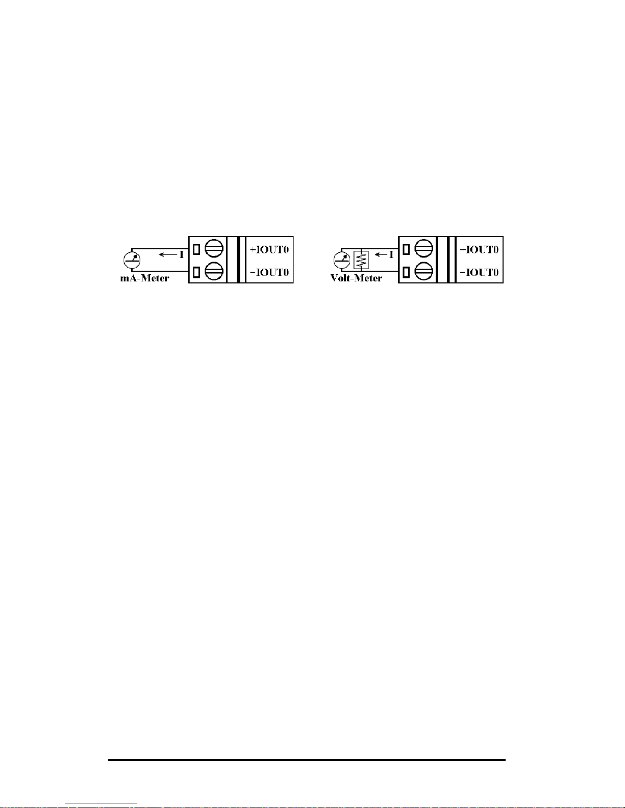
I-7021/21P Current Output Calibration
1. Set the jumper JP1 to select internal power and connect
a current meter to the current output terminal of the
module. If there is no current meter then you can use a
voltage meter with a shunt resistor of 250 ohm and
0.1%. The current (I) can be calculated using the
equation, I = V (voltage) / 250.
2. Warm up the module for at least 30 minutes.
3. Set the type code to 30, 0 ~ 20 mA. Refer to Section
2.1 for details.
4. Send command to output 4 mA. Refer to Section. 2.2
for details.
5. Repeat to send the trim command and check the meter
until the meter’s reading is nearest to 4 mA. Refer to
Section 2.10 for details of sending the trim command.
6. Send the 4 mA calibration command. Refer to Section
2.5 for details.
7. Send command to output 20 mA. Refer to Section. 2.2
for details.
8. Repeat to send the trim command and check the meter
until the meter’s reading is nearest to 20 mA. Refer to
Section 2.10 for details of sending the trim command.
9. Send the 20 mA calibration command. Refer to
Sections 2.7 for details.
I-7021/22/24, M-7022/24/28 User Manual, Rev: B2.3
28
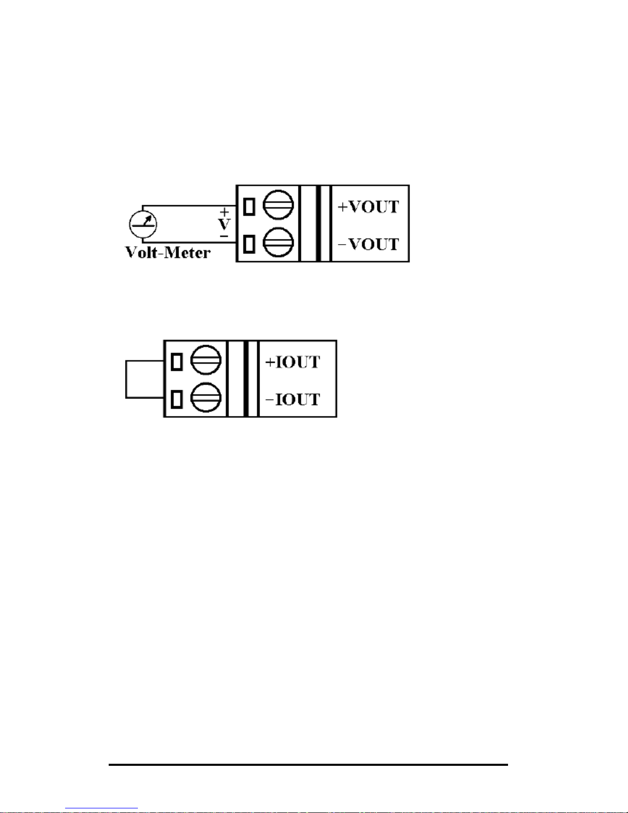
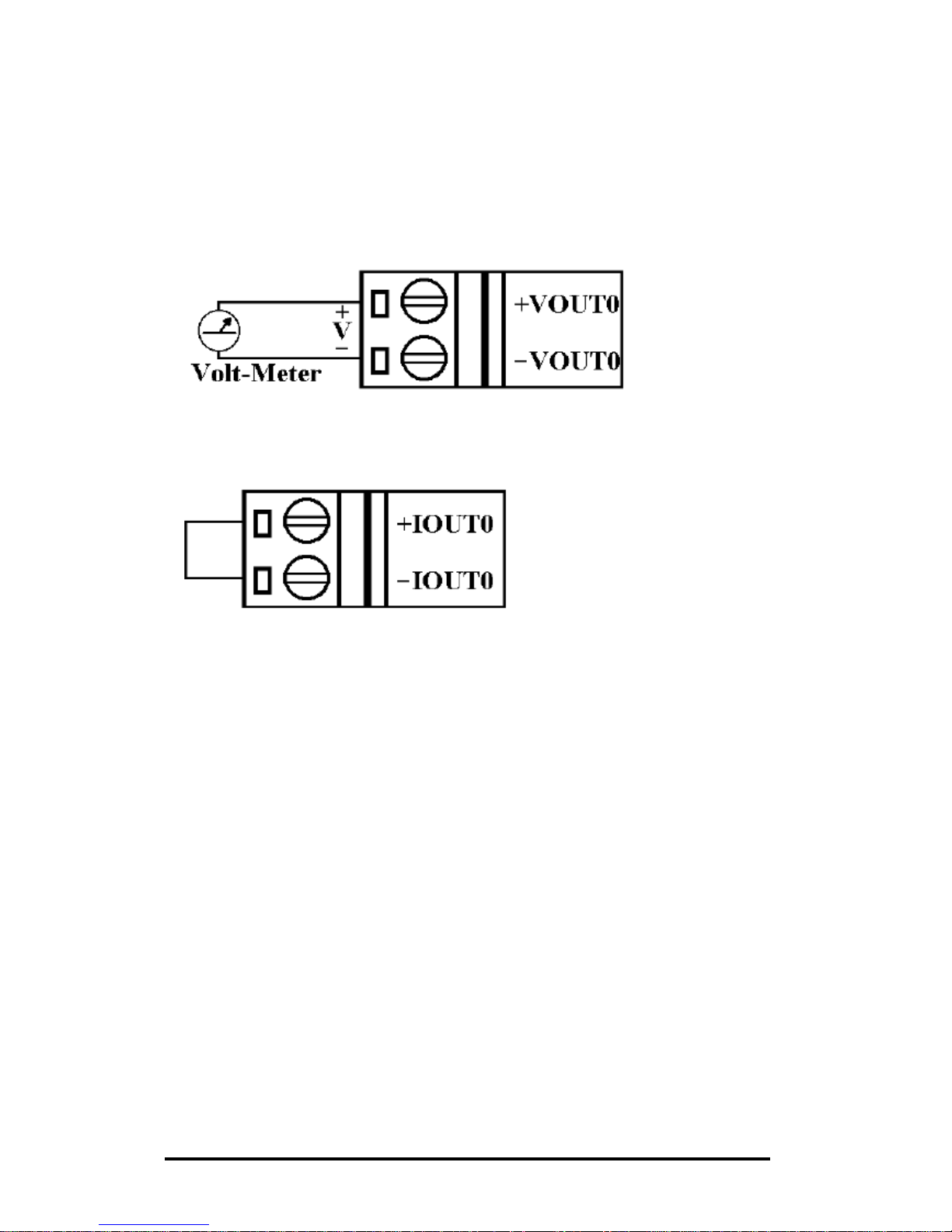
I-7021/21P Voltage Output Calibration
1. Connect a voltage meter to the voltage output terminal
of the module.
Short the current output terminal for the read-back
requirement
2. Warm up the module for at least 30 minutes.
3. Set the type code to 32, 0 ~ 10 V. Refer to Section 2.1
for details.
4. Send command to output 10 V. Refer to Section. 2.2
for details.
5. Repeat to send the trim command and check the meter
until the meter’s reading is nearest to 10 V. Refer to
Section 2.10 for details of sending the trim command.
6. Send the 10 V calibration command. Refer to Section
2.18 for details.
I-7021/22/24, M-7022/24/28 User Manual, Rev: B2.3
29
I-7022/M-7022 Current Output Calibration
1. Set the jumper JP1 to select internal power and connect
a current meter to the current output channel 0 terminal
of the module. If there is no current meter then you
can use a voltage meter with a shunt resistor of 250
ohm and 0.1%. The current (I) can be calculated using
the equation, I = V (voltage) / 250.
2. Warm up the module for at least 30 minutes.
3. Set the type code to 0, 0 ~ 20 mA. Refer to Section
2.24 for details.
4. Send command to output 4 mA. Refer to Section. 2.4
for details.
5. Repeat to send the trim command and check the meter
until the meter’s reading is nearest to 4 mA. Refer to
Section 2.11 for details of sending the trim command.
6. Send the 4 mA calibration command. Refer to Section
2.6 for details.
7. Send command to output 20 mA. Refer to Section. 2.4
for details.
8. Repeat to send the trim command and check the meter
until the meter’s reading is nearest to 20 mA. Refer to
Section 2.11 for details of sending the trim command.
9. Send the 20 mA calibration command. Refer to
Sections 2.8 for details.
10. Repeat steps 1 to 9 for channel 1.
Note:
The M-7022 must be switched to the DCON protocol mode
before calibrating. Refer to Sections 1.12.1 and 3.3.4 for details
of the switching protocol.
I-7021/22/24, M-7022/24/28 User Manual, Rev: B2.3
30
I-7022/M-7022 Voltage Output Calibration
1. Connect a voltage meter to the voltage output channel
0 terminal of the module.
Short the current output terminal for the read-back
requirement
2. Warm up the module for at least 30 minutes.
3. Set the type code to 2, 0 ~ 10 V. Refer to Section 2.24
for details.
4. Send command to output 10 V. Refer to Section. 2.15
for details.
5. Repeat to send the trim command and check the meter
until the meter’s reading is nearest to 10 V. Refer to
Section 2.18 for details of sending the trim command.
6. Send the 10 V calibration command. Refer to Section
2.21 for details.
7. Repeat steps 1 to 9 for channel 1.
Note:
The M-7022 must be switched to the DCON protocol mode
before calibrating. Refer to Section 1.12.1 for details of the
switching protocol.

I-7021/22/24, M-7022/24/28 User Manual, Rev: B2.3
31
I-7024/24R/M-7024/24R Current Output Calibration
(for firmware version A2.9 and earlier)
1. Connect a current meter and an external power source
to the current output channel 0 terminal of the module.
If there is no current meter then you can use a voltage
meter with a shunt resistor of 250 ohm and 0.1%. The
current (I) can be calculated using the equation, I = V
(voltage) / 250.
2. Warm up the module for at least 30 minutes.
3. Set the type code to 30, 0 ~ 20 mA. Refer to Section
2.1 for details.
4. Send command to output 0 mA. Refer to Section. 2.4
for details.
5. Repeat to send the trim command and check the meter
until the meter’s reading is nearest to 0 mA. Refer to
Section 2.11 for details of sending the trim command.
6. Send the 0 mA calibration command. Refer to Section
2.6 for details.
7. Send command to output 20 mA. Refer to Section. 2.4
for details.
8. Repeat to send the trim command and check the meter
until the meter’s reading is nearest to 20 mA. Refer to
Section 2.11 for details of sending the trim command.
9. Send the 20 mA calibration command. Refer to
Sections 2.8 for details.
10. Repeat steps 1 to 9 for channel 1, 2 and 3.
Note:
The M-7024/24R must be switched to the DCON protocol mode
before calibrating. Refer to Sections 1.12.1 for details of the
switching protocol.

I-7021/22/24, M-7022/24/28 User Manual, Rev: B2.3
32
I-7024/24R/M-7024/24R Voltage Output Calibration
(for firmware version A2.9 and earlier)
1. Connect a voltage meter to the voltage output channel
0 terminal of the module.
2. Warm up the module for at least 30 minutes.
3. Set the type code to 33, -10 V ~ +10 V. Refer to
Section 2.1 for details.
4. Send command to output -10 V. Refer to Section. 2.4
for details.
5. Repeat to send the trim command and check the meter
until the meter’s reading is nearest to –10 V. Refer to
Section 2.11 for details of sending the trim command.
6. Send the –10 V calibration command. Refer to Section
2. 6 for details.
7. Send command to output +10 V. Refer to Section. 2.4
for details.
8. Repeat to send the trim command and check the meter
until the meter’s reading is nearest to +10 V. Refer to
Section 2.11 for details of sending the trim command.
9. Send the 10 V calibration command. Refer to Sections
2.8 for details.
10. Repeat steps 1 to 9 for channel 1, 2 and 3.
Note:
The M-7024/24R must be switched to the DCON protocol mode
before calibrating. Refer to Sections 1.12.1 for details of the
switching protocol.

I-7021/22/24, M-7022/24/28 User Manual, Rev: B2.3
33
I-7024/M-7024 with firmware version A3.0 and later,
M-7024L, M-7024U and M-7028 Analog Output
Calibration
1. Warm up the module for at least 30 minutes.
2. If you want to calibrate for current type, then connect a
current meter to the current output channel 0 terminal of
the module. If you want to calibrate for voltage type,
then connect a voltage meter to the voltage output
channel 0 terminal of the module.
3. Set the type code to the type you want to calibrate.
Refer to Section 2.24 for details.
4. Send command to output zero calibration
current/voltage. Refer to Section. 2.4 for details.
5. Repeat to send the trim command and check the meter
until the meter’s reading is nearest to zero calibration
current/voltage. Refer to Section 2.11 for details of
sending the trim command.
6. Send the zero calibration command. Refer to Section
2. 6 for details.
7. Send command to output span calibration
current/voltage. Refer to Section. 2.4 for details.
8. Repeat to send the trim command and check the meter
until the meter’s reading is nearest to span calibration
current/voltage. Refer to Section 2.11 for details of
sending the trim command.
9. Send the span calibration command. Refer to Section
2.8 for details.
10. Repeat steps 1 to 9 for channel 1, 2 and 3.
Notes:
1. The zero/span calibration voltages and currents are shown on
the next page.

I-7021/22/24, M-7022/24/28 User Manual, Rev: B2.3
34
2. The M-7024, M-7024L, M-7024U and M-7028 must be
switched to the DCON protocol mode before calibrating.
Refer to Sections 1.12.1 for details of the switching protocol.
Calibration voltages/current used by the I-7024/M-7204
with firmware version A3.0 and later, M-7024L, M-7024U
and M-7028:
Type Code
0 1 2 3 4
5
Zero
voltage/current
0mA
4mA
0V
-10V
0V
-5V
Span
voltage/current
+20mA
+20mA
+10V
+10V
+5V
+5V

I-7021/22/24, M-7022/24/28 User Manual, Rev: B2.3
35
1.11 Configuration Tables
Baud Rate Setting (CC)
7 6 5 4 3 2 1
0
Data
Baud
Key
Description
Baud
Baud Rate
03: 1200
04: 2400
05: 4800
06: 9600
07: 19200
08: 38400
09: 57600
0A: 115200
Data
Data Format
0: N81
1: N82
2: E81
3: O81
The firmware version that supports the data format other than
N81 is as follows.
Module
Firmware Version
7021
B2.0 and later
7022
B1.2 and later
7024 series
A1.8 and later
7028
All

I-7021/22/24, M-7022/24/28 User Manual, Rev: B2.3
36
Analog Output Type Setting (TT)
Type Code
Output Range
30
0 mA ~ +20 mA
31
+4 mA ~ +20 mA
32
0 V ~ +10 V
33
-10 V ~ +10 V
34
0 ~ +5 V
35
-5 V ~ +5 V
3F
For I-7022/M-7022 only
00
For M-7024U and
M-7028 only
Note:
1. Type 30, 31, and 32 are only applicable to the I-7021,
I-7021P, I-7024, I-7024R, M-7024, M-7024L and
M-7024R.
2. Types 33, 34 and 35 are only applicable to the I-7024,
I-7024R, M-7024, M-7024L and M-7024R.
3. For I-7022 and M-7022, this field must be set to 3F.
For M-7024U and M-7028, this field must be set to 00.

I-7021/22/24, M-7022/24/28 User Manual, Rev: B2.3
37
Data Format Setting (FF)
7 6 5 4 3 2 1
0
0
CS
SR
DF
Key
Description
DF
Data format
00: Engineering unit
01*: % of FSR (full scale range)
10*: 2’s complement hexadecimal
Note: the data format 01 and 10 are only
available to the I-7021/21P, I-7022, M-7022,
M-7024U and M-7028
SR
Slew rate for I-7021, I-7021P, I-7024, I-7024R,
M-7024, M-7024L and M-7024R
V/s
mA/s
V/s
mA/s
0000
immediate
1000
8.0
16.0
0001
0.0625
0.125
1001
16.0
32.0
0010
0.125
0.25
1010
32.0
64.0
0011
0.25
0.5
1011
64.0
128.0
0100
0.5
1.0
1100
128.0
256.0
0101
1.0
2.0
1101
256.0
512.0
0110
2.0
4.0
1110
512.0
1024.0
0111
4.0
8.0
1111
1024.0
2048.0
Note: the setting 1111 is for I-7024, I-7024R,
M-7024, M-7024L and M-7024R only
0 for I-7022, M-7022, M-7024U and M-7028
CS
Checksum setting
0: Disabled
1: Enabled

I-7021/22/24, M-7022/24/28 User Manual, Rev: B2.3
38
Analog Output Type and Data Format Table for
I-7021 and I-7021P
Type Code
Output Range
Data Format
Max.
Min.
30
0 ~ +20 mA
Engineering unit
20.000
00.000
% of FSR
+100.00
+000.00
2’s comp HEX
FFF
000
31
+4 ~ +20 mA
Engineering unit
20.000
04.000
% of FSR
+100.00
+000.00
2’s comp HEX
FFF
000
32
0 ~ 10 V
Engineering unit
10.000
00.000
% of FSR
+100.00
+000.00
2’s comp HEX
FFF
000
Analog Output Type and Data Format Table for
I-7022 and M-7022
Type Code
Output Range
Data Format
Max.
Min.
0
0 ~ 20 mA
Engineering unit
20.000
00.000
% of FSR
+100.00
+000.00
2’s comp HEX
FFF
000
1
4 ~ 20 mA
Engineering unit
20.000
04.000
% of FSR
+100.00
+000.00
2’s comp HEX
FFF
000
2
0 ~ 10 V
Engineering unit
10.000
00.000
% of FSR
+100.00
+000.00
2’s comp HEX
FFF
000
4*
0 ~ 5 V
Engineering unit
05.000
00.000
% of FSR
+100.00
+000.00
2’s comp HEX
FFF
000
Note: The type code 4 is only available to firmware version B1.2 and
later.

I-7021/22/24, M-7022/24/28 User Manual, Rev: B2.3
39
Analog Output Type and Data Format Table for
I-7024, I-7024R, M-7024, M-7024L and M-7024R
Type Code
Output Range
Data Format
Max.
Min.
30
0 ~ +20 mA
Engineering unit
+20.000
+00.000
31
+4 ~ +20 mA
Engineering unit
+20.000
+04.000
32
0 ~ +10 V
Engineering unit
+10.000
+00.000
33
-10 ~ +10 V
Engineering unit
+10.000
-10.000
34
0 ~ +5 V
Engineering unit
+05.000
+00.000
35
-5 V ~ +5 V
Engineering unit
+05.000
-05.000
Analog Output Type and Data Format Table for
M-7024U and M-7028
Type Code
Output Range
Data Format
Max.
Min.
0
0 ~ +20 mA
Engineering unit
+20.000
+00.000
% of FSR
+100.00
+000.00
2’s comp HEX
FFFF
0000
1
+4 ~ +20 mA
Engineering unit
+20.000
+04.000
% of FSR
+100.00
+000.00
2’s comp HEX
FFFF
0000
2
0 ~ +10 V
Engineering unit
+10.000
+00.000
% of FSR
+100.00
+000.00
2’s comp HEX
FFFF
0000
3
-10 ~ +10V
Engineering unit
+10.000
-10.000
% of FSR
+100.00
-100.00
2’s comp HEX
7FFF
8000
4
0 ~ +5 V
Engineering unit
+05.000
+00.000
% of FSR
+100.00
+000.00
2’s comp HEX
FFFF
0000
5
-5 ~ +5 V
Engineering unit
+05.000
-05.000
% of FSR
+100.00
-100.00
2’s comp HEX
7FFF
8000

I-7021/22/24, M-7022/24/28 User Manual, Rev: B2.3
40
Analog Output Configuration for I-7022, M-7022,
M-7204U and M-7028
Analog Output Type Setting (T)
Type Code
Output Range
0
0 mA ~ +20 mA
1
+4 mA ~ +20 mA
2
0 V ~ +10 V
3*
-10 V ~ +10 V
4*
0 V ~ +5 V
5*
-5 V ~ +5 V
Notes:
1. The type code 4 is only available to M-7024U, M-7028 and
I-7022/M-7022 firmware version B1.2 and later.
2. The type code 3 and 5 are only available to M-7024U and
M-7028.
Slew Rate Setting (S)
S
V/s
mA/s
0
Immediate
Immediate
1
0.0625
0.125
2
0.125
0.25
3
0.25
0.5
4
0.5
1.0
5
1.0
2.0
6
2.0
4.0
7
4.0
8.0
8
8.0
16.0
9
16.0
32.0
A
32.0
64.0
B
64.0
128.0
C
128.0
256.0
D
256.0
512.0
E
512.0
1024.0

I-7021/22/24, M-7022/24/28 User Manual, Rev: B2.3
41
1.12 M-7000 Notes
The main difference between the I-7000 and M-7000
series is that the M-7000 series has additional support for
the Modbus RTU communication protocol, which is the
default protocol of the M-7000 series. The
communication Baud Rates for the Modbus RTU protocol
can be in the range of 1200 bps to 115200 bps.
Modbus functions supported by the module are described
in Chapter 3.
1.12.1 Protocol Switching
To switch to the DCON protocol:
1. Set Modbus register 00257 to 1.
2. After a power-on reset, the communication protocol
will be changed to DCON.
To switch to the Modbus RTU protocol:
1. Sends the $AAPN command and set N to a value of 1.
Note that the INIT* terminal should be connected to
the GND terminal, or the slide switch on the rear side
of the module should be set to the INIT position. See
Section 2.31 for details.
2. After a power-on reset, the communication protocol
will be changed to the Modbus RTU protocol.

I-7021/22/24, M-7022/24/28 User Manual, Rev: B2.3
42
1.12.2 INIT Mode
When the module is powered on with the INIT* pin
connected to the GND pin or the rear slide switch set to
the INIT position as shown in the figure below, the
module is in INIT mode, (see Section A.1 for details), and
the communication settings are as follows:
1. Address: 00
2. Baud Rate: 9600 bps
3. No checksum
4. Protocol: DCON
If communication with the module is not possible, set the
module to the INIT mode and use the above settings to
communicate with the module. To read the current
settings, send the commands $AA2, (see Section 2.9), and
$AAP, (see Section 2.30). To set new settings, send the
commands %AANNTTCCFF, (see Section 2.1) and
$AAPN, (see Section 2.31). The new communication
settings will be effective after the next power-on reset.

I-7021/22/24, M-7022/24/28 User Manual, Rev: B2.3
43
1.13 Mounting
1.13.1 Din-Rail Mounting
There are three new DIN rail models available. Each is
made of stainless steel, which is stronger than those made
of aluminum. There is a screw at one end and a ring
terminal is included so that it can be easily connected to
the earth ground. The three new DIN rail models are as
follows.
Part number
Max. number of modules
Dimensions
DRS-360
5
360mm x 35mm

I-7021/22/24, M-7022/24/28 User Manual, Rev: B2.3
44
Part number
Max. number of modules
Dimensions
DRS-240
3
240mm x 35mm
Part number
Max. number of modules
Dimensions
DRS-125
2
125mm x 35mm
Note: It is recommended that a 16 – 14 AWG wire is used
to connect the DIN rail to the earth ground.

I-7021/22/24, M-7022/24/28 User Manual, Rev: B2.3
45
1.13.2 Piggyback Mounting
For I-7021, I-7021P, I-7022, and M-7022 modules
For other modules

I-7021/22/24, M-7022/24/28 User Manual, Rev: B2.3
46
1.13.3 Wall Mounting

I-7021/22/24, M-7022/24/28 User Manual, Rev: B2.3
47
1.14 Technical Support
Should you encounter any problems while using the
I-7000 and M-7000 module, and are unable to find the
help you need in this manual or on our website, please
contact ICP DAS Product Support.
Email: service@icpdas.com
Website: http://www.icpdas.com.tw/contact_us/contact_us.html
When requesting technical support, be prepared to provide
the following information about your system:
1. Module name and serial number: The serial number can
be found printed on the barcode label attached to the
cover of the module.
2. Firmware version: See Section 2.27 for information
regarding the command used to identify the firmware
version. Or, read the Modbus registers 40481 and
40482 for Modbus protocol.
3. Host configuration (type and operating system)
4. If the problem is reproducible, please give full details
describing the procedure used to reproduce the problem.
5. Any specific error messages displayed. If a dialog box
with an error message is displayed, please include the
full text of the dialog box, including the text in the title
bar.
6. If the problem involves other programs or hardware
devices, please describe the details of the problem in
full.
7. Any comments and suggestions related to the problem
are welcome.
ICP DAS will reply to your request by email within three
business days.

I-7021/22/24, M-7022/24/28 User Manual, Rev: B2.3
48
2. DCON Protocol
All communication with I-7000 modules consists of
commands generated by the host and responses
transmitted by the I-7000 modules. Each module has a
unique ID number that is used for addressing purposes and
is stored in non-volatile memory. The ID is 01 by default
and can be changed using a user command. All
commands to the modules contain the ID address,
meaning that only the addressed module will respond.
The only exception to this is command ~** (Section 2.34),
which are sent to all modules, but the modules do not
reply to the command.
Command Format:
Leading
Character
Module
Address
Command
[CHKSUM]
CR
Response Format:
Leading
Character
Module
Address
Data
[CHKSUM]
CR
CHKSUM A 2-character checksum which is present
when the checksum setting is enabled. See
Sections 1.11 (Data Format Setting) and 2.1
for details.
CR End of command character, carriage return
(0x0D)

I-7021/22/24, M-7022/24/28 User Manual, Rev: B2.3
49
Checksum Calculation:
1. Calculate the ASCII code sum of all the characters in
the command/response string except for the carriage
return character (CR).
2. The checksum is equal to the sum masked by 0FFh.
Example:
Command string: $012(CR)
1. Sum of the string = “$”+”0”+”1”+”2” =
24h+30h+31h+32h = B7h
2. Therefore the checksum is B7h, and so
CHKSUM = “B7”
3. The command string with the checksum = $012B7(CR)
Response string: !01200600(CR)
1. Sum of the string =
“!”+”0”+”1”+”2”+”0”+”0”+”6”+”0”+”0” =
21h+30h+31h+32h+30h+30h+36h+30h+30h = 1AAh
2. Therefore the checksum is AAh, and so
CHKSUM = “AA”
3. The response string with the checksum
= !01200600AA(CR)
Note:
All characters should be in upper case.

I-7021/22/24, M-7022/24/28 User Manual, Rev: B2.3
50
General Command Sets
Command
Response
Description
Section
%AANNTTCCFF
!AA
Sets the module configuration
2.1
$AA2
!AATTCCFF
Reads the module configuration
2.9
$AA5
!AAS
Reads the module reset status
2.14
$AAF
!AA(Data)
Reads the firmware version
2.27
$AAI
!AAS
Reads the INIT terminal status
2.28
$AAM
!AA(Data)
Reads the module name
2.29
$AAP
!AASC
Reads the communication protocol
2.30
$AAPN
!AA
Sets the communication protocol
2.31
~AAO(Name)
!AA
Sets the module name
2.33
I-7021/21P Analog Output Command Sets
Command
Response
Description
Section
#AA(Data)
>
Sets the analog output channel
2.2
$AA0
!AA
Performs a 4mA calibration
2.5
$AA1
!AA
Performs a 20mA calibration
2.7
$AA3VV
!AA
Adjusts the analog output for calibration
2.10
$AA4
!AA
Sets the current output value as power-on
value
2.12
$AA6
!AA(Data)
Reads the last written analog output value
2.15
$AA7
!AA
Performs a 10V calibration
2.18
$AA8
!AA(Data)
Reads the analog output channel via an
analog-to-digital converter
2.21
I-7022/M-7022 Analog Output Command Sets
Command
Response
Description
Section
#AAN(Data)
>
Sets the analog output of a channel
2.4
$AA0N
!AA
Performs a 4mA calibration of a channel
2.6
$AA1N
!AA
Performs a 20mA calibration of a channel
2.8
$AA3NVV
!AA
Adjusts the analog output of a channel for
calibration
2.11
$AA4N
!AA
Sets the current output value of a channel as
power-on value
2.13
$AA6N
!AA(Data)
Reads the last written analog output value of
a channel
2.17
$AA7N
!AA
Performs a 10V calibration of a channel
2.19

I-7021/22/24, M-7022/24/28 User Manual, Rev: B2.3
51
$AA8N
!AA(Data)
Reads the analog output channel via an
analog-to-digital converter
2.22
$AA9N
!AATS
Reads the analog output configuration of a
channel
2.23
$AA9NTS
!AA
Sets the analog output configuration of a
channel
2.24
I-7024/I-7024R/M-7024/M-7024L/M-7024R Analog Output Command Sets
Command
Response
Description
Section
#AAN(Data)
>
Sets the analog output of a channel
2.4
$AA0N
!AA
Performs a 4mA or –10V calibration of a
channel
2.6
$AA1N
!AA
Performs a 20mA or +10V calibration of a
channel
2.8
$AA3NVV
!AA
Adjusts the analog output of a channel for
calibration
2.11
$AA4N
!AA
Sets the current output value of a channel as
power-on value
2.13
$AA6N
!AA(Data)
Reads the last written analog output value of
a channel
2.17
$AA7N
!AA
Reads the power-on value of a channel
2.20
$AA8N
!AA(Data)
Reads the current analog output of a channel
2.22
M-7024U Analog Output Command Sets
Command
Response
Description
Section
#AAN(Data)
>
Sets the analog output of a channel
2.4
$AA0N
!AA
Performs zero calibration of a channel
2.6
$AA1N
!AA
Performs span calibration of a channel
2.8
$AA3NVV
!AA
Adjusts the analog output of a channel for
calibration
2.11
$AA4N
!AA
Sets the current output value of a channel as
power-on value
2.13
$AA6N
!AA(Data)
Reads the last written analog output value of
a channel
2.17
$AA7N
!AA
Reads the power-on value of a channel
2.20
$AA8N
!AA(Data)
Reads the current analog output of a channel
2.22
$AA9N
!AATS
Reads the analog output configuration of a
channel
2.23
$AA9NTS
!AA
Sets the analog output configuration of a
channel
2.24
@AABB
!AAHH
Reads the retained analog output status
2.45
@AABBHH
!AA
Sets the retained analog output status
2.46

I-7021/22/24, M-7022/24/28 User Manual, Rev: B2.3
52
M-7028 Analog Output Command Sets
Command
Response
Description
Section
#AAN(Data)
>
Sets the analog output of a channel
2.4
$AA0N
!AA
Performs zero calibration of a channel
2.6
$AA1N
!AA
Performs span calibration of a channel
2.8
$AA3NVV
!AA
Adjusts the analog output of a channel for
calibration
2.11
$AA4N
!AA
Sets the current output value of a channel as
power-on value
2.13
$AA6N
!AA(Data)
Reads the last written analog output value of
a channel
2.17
$AA7N
!AA
Reads the power-on value of a channel
2.20
$AA8N
!AA(Data)
Reads the current analog output of a channel
2.22
$AA9N
!AATS
Reads the analog output configuration of a
channel
2.23
$AA9NTS
!AA
Sets the analog output configuration of a
channel
2.24
I-7024R/M-7024R Digital Input Command Sets
Command
Response
Description
Section
#AAN
!AA(Data)
Reads the counter data of a digital channel
2.3
$AA6
!(Data)
Reads the digital input status
2.16
$AACN
!AA
Resets the counter data of a digital channel
2.26
@AACECN*
!AA
Resets the counter data of a digital channel
2.47
@AADI*
!AA000II
Reads the digital input status
2.48
@AARECN*
!AA(Data)
Reads the counter data of a digital channel
2.50
*Note: It is recommended to use these commands for firmware version
A2.3 and later.
M-7024U Digital Input and Output Command Sets
Command
Response
Description
Section
@AACECN
!AA
Resets the counter data of a digital channel
2.47
@AADI
!AA0OOII
Reads the digital output and input status
2.48
@AADO
!AA
Sets the digital output value
2.49
@AARECN
!AA(Data)
Reads the counter data of a digital channel
2.50
~AA4
!AAPPSS
Reads the power on and safe digital output
value
2.40
~AA5PPSS
!AA
Sets the power on and safe digital output
value
2.44

I-7021/22/24, M-7022/24/28 User Manual, Rev: B2.3
53
Host Watchdog Command Sets
Command
Response
Description
Section
~**
No Response
Host is OK
2.34
~AA0
!AASS
Reads the host watchdog status
2.35
~AA1
!AA
Resets the host watchdog status
2.36
~AA2
!AAETT
Reads the host watchdog timeout settings
2.37
~AA3ETT
!AA
Sets the host watchdog timeout settings
2.38
~AA4
!AA(Data)
Reads the analog output safe value
2.39
~AA4N
!AA(Data)
Reads the safe value of an analog output
channel
2.41
~AA5
!AA
Sets the current analog output value as
safe value
2.42
~AA5N
!AA
Sets the current analog output value as
safe value for a channel
2.43

I-7021/22/24, M-7022/24/28 User Manual, Rev: B2.3
54
2.1 %AANNTTCCFF
Description:
Sets the configuration of an analog output module.
Syntax:
%AANNTTCCFF[CHKSUM](CR)
% Delimiter character
AA Address of the module to be configured in
hexadecimal format (00 to FF)
NN New address of the module in hexadecimal format
(00 to FF)
TT New type code, see Section 1.11 for details. For
the I-7022, M-7022, M-7024U and M-7028, this
field should be set to 3F, 00 for M-7024U and
M-7208, and use the $AA9NTS command to set
the type of each channel, see Section 2.24 for
details.
CC New Baud Rate code, see Section 1.11 for details.
The module must be switched to INIT* mode in
order to change Baud Rates. See Section A.1 for
details.
FF Used to set the data format, checksum, and slew
rate settings (Section 1.11). For the I-7022,
M-7022, M-7024U and M-7208, use the
$AA9NTS command to set the slew rate of each
channel, see Section 2.24 for details. The module
must be switched to INIT* mode in order to
change the checksum setting. See Section A.1 for
details.
I-7021, I-7021P, I-7022, I-7024, I-7024R
M-7022, M-7024, M-7024L, M-7024R, M-7024U, M-7028

I-7021/22/24, M-7022/24/28 User Manual, Rev: B2.3
55
Response:
Valid Command: !AA[CHKSUM](CR)
Invalid Command: ?AA[CHKSUM](CR)
! Delimiter for a valid command
? Delimiter for an invalid command. If the Baud
Rate or checksum settings are changed without
connecting the INIT* terminal to ground, the
module will return an invalid command.
AA Address of the module in hexadecimal format (00
to FF)
There will be no response if the command syntax is
incorrect, there is a communication error, or there is no
module with the specified address.
Examples:
Command: %0102300600 Response: !02
Changes the address of module 01 to 02. The module
returns a valid response.
Command: %0101300A00 Response: ?01
Changes the Baud Rate of module 01 to 115200bps.
The module returns an invalid command, because it
is not in INIT* mode.
Command: %0101300A00 Response: !01
Changes the Baud Rate of module 01 to 115200bps
and the module is in INIT* mode. The module
returns a valid response.
I-7021, I-7021P, I-7022, I-7024, I-7024R
M-7022, M-7024, M-7024L, M-7024R, M-7024U, M-7028

I-7021/22/24, M-7022/24/28 User Manual, Rev: B2.3
56
Related Commands:
Section 2.9 $AA2
Related Topics:
Section 1.11 Configuration Tables, Section A.1 INIT
Mode
Note:
Changes to the address, type code, data format and slew
rate settings take effect immediately after a valid
command is received. Changes to the Baud Rate and
checksum settings take effect on the next power-on reset.
I-7021, I-7021P, I-7022, I-7024, I-7024R
M-7022, M-7024, M-7024L, M-7024R, M-7024U, M-7028

I-7021/22/24, M-7022/24/28 User Manual, Rev: B2.3
57
2.2 #AA(Data)
Description:
Writes the data to analog output channel.
Syntax:
#AA(Data)[CHKSUM](CR)
# Delimiter character
AA Address of the module to be written (00 to FF)
(Data) Data to be written to the analog output channel,
see Section 1.11 for the data format.
Response:
Valid Command: >[CHKSUM](CR)
Out of Range: ?[CHKSUM](CR)
Ignored: 
> Delimiter character for a valid command
? Delimiter character indicates that the data is out
of range. If it is over range, then the output will
be set to the maximum value of the range. If it
is under range, then the output will be set to the
minimum value of the range.
! Delimiter character indicates that the command
is ignored, because the host watchdog timeout
occurs. The output is set to the safe value.
There will be no response if the command syntax is
incorrect, there is a communication error, or there is no
module with the specified address.
I-7021, I-7021P

I-7021/22/24, M-7022/24/28 User Manual, Rev: B2.3
58
Examples:
Command: $012 Response: !01300600
Reads the configuration of module 01. It returns:
output type 0 mA ~ 20 mA, engineering data format
and output changing immediately.
Command: #0105.000 Response: >
Sets module 01 to output 5 mA. The module returns a
valid response.
Command: #0125.000 Response: ?
Sets module 01 to output 25 mA. The module returns
an out of range response and the output is set to 20 mA.
Command: $032 Response: !03300602
Reads the configuration of module 01. It returns:
output type 0 mA ~ 20 mA, hexadecimal data format
and output changing immediately.
Command: #03800 Response: >
Sets module 03 to output 800h (10 mA). The module
returns a valid response.
Related Commands:
Section 2.1 %AANNTTCCFF, Section 2.9 $AA2
Related Topics:
Section 1.11 Configuration Tables, Section A.5 Analog
Output
Note:
This command is only applicable to the I-7021 and
I-7021P.
I-7021, I-7021P

I-7021/22/24, M-7022/24/28 User Manual, Rev: B2.3
59
2.3 #AAN
Description:
Reads the counter data of a specified digital input channel.
Syntax:
#AAN[CHKSUM](CR)
# Delimiter character
AA Address of the module to be read (00 to FF)
N The channel to be read, zero based.
Response:
Valid Command: !AA(Data)[CHKSUM](CR)
Invalid Command: ?AA[CHKSUM](CR)
! Delimiter character for a valid command
? Delimiter character for an invalid command. An
invalid command is returned if the specified
channel is incorrect.
AA Address of the module in hexadecimal format
(00 to FF)
(Data) Five digits data of the counter value of the
specified channel.
There will be no response if the command syntax is
incorrect, there is a communication error, or there is no
module with the specified address.
I-7024R
M-7024R

I-7021/22/24, M-7022/24/28 User Manual, Rev: B2.3
60
Examples:
Command: #032 Response: !0302513
Reads counter data from channel 2 of module 03 and
returns the counter value 2513.
Related Commands:
Section 2.26 $AACN, Section 2.47 @AACECN, Section
2.50 @AARECN
Notes:
1. This command is only applicable to the I-7024R and
M-7024R.
2. For I-7024R and M-7024R with firmware version A2.3
and later, it is recommended to use @AARECN
command to read the counter value.
I-7024R
M-7024R

I-7021/22/24, M-7022/24/28 User Manual, Rev: B2.3
61
2.4 #AAN(Data)
Description:
Writes the data to a specified analog output channel.
Syntax:
#AAN(Data)[CHKSUM](CR)
# Delimiter character
AA Address of the module to be written (00 to FF)
N The analog output channel to be written, zero
based.
(Data) Data to be written to the analog output channel,
see Section 1.11 for the data format.
Response:
Valid Command: >[CHKSUM](CR)
Out of Range: ?[CHKSUM](CR)
Ignored: 
> Delimiter character for a valid command
? Delimiter character indicates that the data is out
of range. If it is over range, then the output will
be set to the maximum value of the range. If it
is under range, then the output will be set to the
minimum value of the range.
! Delimiter character indicates that the command
is ignored, because the host watchdog timeout
occurs. The output is set to the safe value.
There will be no response if the command syntax is
incorrect, there is a communication error, or there is no
module with the specified address.
I-7022, I-7024, I-7024R
M-7022, M-7024, M-7024L, M-7024R, M-7024U, M-7028

I-7021/22/24, M-7022/24/28 User Manual, Rev: B2.3
62
Examples for I-7022 and M-7022:
Command: $012 Response: !013F0600
Reads the configuration of module 01. It returns:
engineering data format.
Command: $0190 Response: !0110
Reads the configuration of analog output channel 0 of
module 01. It returns: output type 4 mA to 20 mA and
output changing immediately.
Command: #01005.000 Response: >
Sets channel 0 of module 01 to output 5 mA. The
module returns a valid response.
Command: #01025.000 Response: ?
Sets channel 0 of module 01 to output 25 mA. The
module returns an out of range response and the output
is set to 20 mA.
Examples for I-7024, I-7024R, M-7024, M-7024L
and M-7024R:
Command: $012 Response: !01300600
Reads the configuration of module 01. It returns:
output type 0 mA ~ 20 mA, engineering data format
and output changing immediately.
Command: #010+05.000 Response: >
Sets channel 0 of module 01 to output 5 mA. The
module returns a valid response.
Command: #010+25.000 Response: ?
Sets channel 0 of module 01 to output 25 mA. The
module returns an out of range response and the output
is set to 20 mA.
I-7022, I-7024, I-7024R
M-7022, M-7024, M-7024L, M-7024R, M-7024U, M-7028

I-7021/22/24, M-7022/24/28 User Manual, Rev: B2.3
63
Examples for M-7024U an M-7208:
Command: $012 Response: !01000600
Reads the configuration of module 01. It returns:
engineering data format.
Command: $0190 Response: !0110
Reads the configuration of analog output channel 0 of
module 01. It returns: output type 4 mA to 20 mA and
output changing immediately.
Command: #010+05.000 Response: >
Sets channel 0 of module 01 to output 5 mA. The
module returns a valid response.
Command: #010+25.000 Response: ?
Sets channel 0 of module 01 to output 25 mA. The
module returns an out of range response and the output
is set to 20 mA.
Related Commands:
Section 2.1 %AANNTTCCFF, Section 2.9 $AA2
Related Topics:
Section 1.11 Configuration Tables, Section A.5 Analog
Output
Note:
This command is only applicable to the I-7022, I-7024,
I-7024R, M-7022, M-7024, M-7024L, M-7024R,
M-7024U and M-7028.
I-7022, I-7024, I-7024R
M-7022, M-7024, M-7024L, M-7024R, M-7024U, M-7028

I-7021/22/24, M-7022/24/28 User Manual, Rev: B2.3
64
2.5 $AA0
Description:
I-7021, I-7021P: Performs a 4 mA calibration.
I-7021A: Performs a zero calibration.
Syntax:
$AA0[CHKSUM](CR)
$ Delimiter character
AA Address of the module to be calibrated (00 to FF)
0 Command for the 4 mA/zero calibration
Response:
Valid Command: !AA[CHKSUM](CR)
Invalid Command: ?AA[CHKSUM](CR)
! Delimiter character for a valid command
? Delimiter character for an invalid command
AA Address of the responding module (00 to FF)
There will be no response if the command syntax is
incorrect, there is a communication error, or there is no
module with the specified address.
Examples:
Command: $010 Response: !01
Performs a 4 mA output calibration on module 01
and returns a valid response.
Related Commands:
Section 2.7 $AA1, Section 2.10 $AA3VV
I-7021, I-7021A, I-7021P

I-7021/22/24, M-7022/24/28 User Manual, Rev: B2.3
65
Related Topics:
Section 1.10 Calibration
Note:
This command is only applicable to the I-7021, I-7021A,
and I-7021P.
I-7021, I-7021A, I-7021P

I-7021/22/24, M-7022/24/28 User Manual, Rev: B2.3
66
2.6 $AA0N
Description:
I-7022/M-7022
Performs 4 mA
calibration
I-7024/I-7024R/M-7024/M-7024R
firmware version A2.9 and earlier
Performs 0 mA or
-10 V calibration
M-7022A/M-7024L/M-7024U/
M-7028, I-7024/I-7024R/M-7024/
M-7024R firmware version A3.0
and later
Performs a zero
calibration
Syntax:
$AA0N[CHKSUM](CR)
$ Delimiter character
AA Address of the module to be calibrated (00 to FF)
0 Command for the 4 mA/0 mA/-10 V/zero
calibration
N Specifies the channel to be calibrated, zero based
Response:
Valid Command: !AA[CHKSUM](CR)
Invalid Command: ?AA[CHKSUM](CR)
! Delimiter character for a valid command
? Delimiter character for an invalid command
AA Address of the responding module (00 to FF)
There will be no response if the command syntax is
incorrect, there is a communication error, or there is no
module with the specified address.
I-7022, I-7024, I-7024R
M-7022, M-7022A, M-7024, M-7024L, M-7024R, M-7024U, M-7028

I-7021/22/24, M-7022/24/28 User Manual, Rev: B2.3
67
Examples:
Command: $0101 Response: !01
Performs a zero calibration on channel 1 of module
01 and returns a valid response.
Related Commands:
Section 2.8 $AA1N, Section 2.11 $AA3NVV
Related Topics:
Section 1.10 Calibration
Notes:
This command is only applicable to the I-7022, I-7024,
I-7024R, M-7022, M-7022A, M-7024, M-7024L,
M-7024R, M-7024U and M-7028.
I-7022, I-7024, I-7024R
M-7022, M-7022A, M-7024, M-7024L, M-7024R, M-7024U, M-7028

I-7021/22/24, M-7022/24/28 User Manual, Rev: B2.3
68
2.7 $AA1
Description:
I-7021, I-7021P: Performs a 20 mA calibration.
I-7021A: Performs a span calibration.
Syntax:
$AA1[CHKSUM](CR)
$ Delimiter character
AA Address of the module to be calibrated (00 to FF)
1 Command for the 20 mA/span calibration
Response:
Valid Command: !AA[CHKSUM](CR)
Invalid Command: ?AA[CHKSUM](CR)
! Delimiter character for a valid command
? Delimiter character for an invalid command
AA Address of the responding module (00 to FF)
There will be no response if the command syntax is
incorrect, there is a communication error, or there is no
module with the specified address.
Examples:
Command: $011 Response: !01
Performs a 20 mA output calibration on module 01
and returns a valid response.
Related Commands:
Section 2.5 $AA0, Section 2.10 $AA3VV
I-7021, I-7021A, I-7021P

I-7021/22/24, M-7022/24/28 User Manual, Rev: B2.3
69
Related Topics:
Section 1.10 Calibration
Note:
This command is only applicable to the I-7021, I-7021A,
and I-7021P.
I-7021, I-7021A, I-7021P

I-7021/22/24, M-7022/24/28 User Manual, Rev: B2.3
70
2.8 $AA1N
Description:
I-7022/M-7022
Performs 20 mA
calibration
I-7024/I-7024R/M-7024/M-7024R
firmware version A2.9 and earlier
Performs 20 mA
or +10 V
calibration
M-7022A/M-7024L/M-7024U/
M-7028, I-7024/I-7024R/M-7024/
M-7024R firmware version A3.0
and later
Performs a span
calibration
Syntax:
$AA1N[CHKSUM](CR)
$ Delimiter character
AA Address of the module to be calibrated (00 to FF)
1 Command for the 20 mA/+10 V/span calibration
N Specifies the channel to be calibrated, zero based
Response:
Valid Command: !AA[CHKSUM](CR)
Invalid Command: ?AA[CHKSUM](CR)
! Delimiter character for a valid command
? Delimiter character for an invalid command
AA Address of the responding module (00 to FF)
There will be no response if the command syntax is
incorrect, there is a communication error, or there is no
module with the specified address.
I-7022, I-7024, I-7024R
M-7022, M-7022A, M-7024, M-7024L, M-7024R, M-7024U, M-7028

I-7021/22/24, M-7022/24/28 User Manual, Rev: B2.3
71
Examples:
Command: $0111 Response: !01
Performs a span calibration on channel 1 of module
01 and returns a valid response.
Related Commands:
Section 2.6 $AA0N, Section 2.11 $AA3NVV
Related Topics:
Section 1.10 Calibration
Notes:
This command is only applicable to the I-7022, I-7024,
I-7024R, M-7022, M-7022A, M-7024, M-7024L,
M-7024R, M-7024U and M-7028.
I-7022, I-7024, I-7024R
M-7022, M-7022A, M-7024, M-7024L, M-7024R, M-7024U, M-7028

I-7021/22/24, M-7022/24/28 User Manual, Rev: B2.3
72
2.9 $AA2
Description:
Reads the module configuration.
Syntax:
$AA2[CHKSUM](CR)
$ Delimiter character
AA Address of the module to be read (00 to FF)
2 Command to read the module configuration
Response:
Valid Command: !AATTCCFF[CHKSUM](CR)
Invalid Command: ?AA[CHKSUM](CR)
! Delimiter character for a valid command
? Delimiter character for an invalid command
AA Address of the responding module (00 to FF)
TT Type code of the module. For the I-7022,
M-7022, M-7024U and M-7028, this field is to
3F and 00 for M-7024U and M-7028, see
Section 1.110 for details.
CC Baud Rate code of the module, see Section 1.11
for details.
FF Data format, checksum settings and slew rate
settings of the module, see Section 1.11 for
details.
There will be no response if the command syntax is
incorrect, there is a communication error, or there is no
module with the specified address.
I-7021, I-7021P, I-7022, I-7024, I-7024R, M-7021A
M-7022, M-7022A, M-7024, M-7024L, M-7024R, M-7024U, M-7028

I-7021/22/24, M-7022/24/28 User Manual, Rev: B2.3
73
Examples:
Command: $012 Response: !01300600
Reads the configuration of module 01.
Command: $022 Response: !02330602
Reads the configuration of module 02.
Related Commands:
Section 2.1 %AANNTTCCFF
Related Topics:
Section 1.11 Configuration Tables
I-7021, I-7021P, I-7022, I-7024, I-7024R, M-7021A
M-7022, M-7022A, M-7024, M-7024L, M-7024R, M-7024U, M-7028

I-7021/22/24, M-7022/24/28 User Manual, Rev: B2.3
74
2.10 $AA3VV
Description:
Adjusts the analog output for calibration.
Syntax:
$AA3VV[CHKSUM](CR)
$ Delimiter character
AA Address of the module to be adjusted (00 to FF)
3 Command to adjust the analog output
VV A two-digit 2’s complement hexadecimal value
to adjust the analog output. The value of 00 to
5F is to increase 0 to 95 counts and FF to A1 is
to decrease 1 to 95 counts, where each count is
about 4.88uA or 2.44mV.
Response:
Valid Command: !AA[CHKSUM](CR)
Invalid Command: ?AA[CHKSUM](CR)
! Delimiter character for a valid command
? Delimiter character for an invalid command
AA Address of the responding module (00 to FF)
There will be no response if the command syntax is
incorrect, there is a communication error, or there is no
module with the specified address.
I-7021, I-7021P

I-7021/22/24, M-7022/24/28 User Manual, Rev: B2.3
75
Examples:
Command: $0131F Response: !01
Sets the analog output of module 01 to be
increased by 31 and returns a valid response.
Related Commands:
Section 2.5 $AA0, Section 2.7 $AA1
Note:
This command is only applicable to the I-7021/21P.
I-7021, I-7021P

I-7021/22/24, M-7022/24/28 User Manual, Rev: B2.3
76
2.11 $AA3NVV
Description:
Adjusts the analog output of a specified channel for
calibration.
Syntax:
$AA3NVV[CHKSUM](CR)
$ Delimiter character
AA Address of the module to be adjusted (00 to FF)
3 Command to adjust the analog output
N The channel to be adjusted, zero based
VV A two-digit 2’s complement hexadecimal value
to adjust the analog output. The value of 00 to
5F is to increase 0 to 95 counts and FF to A1 is
to decrease 1 to 95 counts, where each count is
about 4.88uA or 2.44mV for I-7022, M-7022
and M-7028, 2.44uA or 1.22mV for I-7024/24R
and M-7024/24R, 0.61uA or 0.30mA for
M-7024U.
Response:
Valid Command: !AA[CHKSUM](CR)
Invalid Command: ?AA[CHKSUM](CR)
! Delimiter character for a valid command
? Delimiter character for an invalid command
AA Address of the responding module (00 to FF)
I-7022, I-7024, I-7024R
M-7022, M-7024, M-7024L, M-7024R, M-7024U, M-7028

I-7021/22/24, M-7022/24/28 User Manual, Rev: B2.3
77
There will be no response if the command syntax is
incorrect, there is a communication error, or there is no
module with the specified address.
Examples:
Command: $01321F Response: !01
Sets the analog output channel 2 of module 01 to
be increased by 31 and returns a valid response.
Related Commands:
Section 2.6 $AA0N, Section 2.8 $AA1N
Note:
This command is only applicable to the I-7022, M-7022,
I-7024, I-7024R, M-7024, M-7024L, M-7024R, M-7024U
and M-7028.
I-7022, I-7024, I-7024R
M-7022, M-7024, M-7024L, M-7024R, M-7024U, M-7028

I-7021/22/24, M-7022/24/28 User Manual, Rev: B2.3
78
2.12 $AA4
Description:
Sets the current output as the power-on value.
Syntax:
$AA4[CHKSUM](CR)
$ Delimiter character
AA Address of the module to be set (00 to FF)
4 Command to set the power on value
Response:
Valid Command: !AA[CHKSUM](CR)
Invalid Command: ?AA[CHKSUM](CR)
! Delimiter character for a valid command
? Delimiter character for an invalid command
AA Address of the responding module (00 to FF)
There will be no response if the command syntax is
incorrect, there is a communication error, or there is no
module with the specified address.
Examples:
Command: #0100.000 Response: >
Sets the output of module 01 to 0.0mA and returns
a valid response.
Command: $014 Response: !01
Sets the current output of module 01 as the poweron value and returns a valid response.
I-7021, I-7021P

I-7021/22/24, M-7022/24/28 User Manual, Rev: B2.3
79
Related Commands:
Section 2.2 #AA(data)
Note:
This command is only applicable to the I-7021/21P.
I-7021, I-7021P

I-7021/22/24, M-7022/24/28 User Manual, Rev: B2.3
80
2.13 $AA4N
Description:
Sets the current output of a specified channel as the
power-on value.
Syntax:
$AA4N[CHKSUM](CR)
$ Delimiter character
AA Address of the module to be set (00 to FF)
4 Command to set the power on value
N The channel to be set, zero based
Response:
Valid Command: !AA[CHKSUM](CR)
Invalid Command: ?AA[CHKSUM](CR)
! Delimiter character for a valid command
? Delimiter character for an invalid command
AA Address of the responding module (00 to FF)
There will be no response if the command syntax is
incorrect, there is a communication error, or there is no
module with the specified address.
Examples:
Command: #01100.000 Response: >
Sets the output of channel 1 of module 01 to
0.0mA and returns a valid response.
I-7022, I-7024, I-7024R
M-7022, M-7024, M-7024L, M-7024R, M-7024U, M-7028

I-7021/22/24, M-7022/24/28 User Manual, Rev: B2.3
81
Command: $0141 Response: !01
Sets the current output of channel 1 of module 01
as the power-on value and returns a valid response.
Related Commands:
Section 2.4 #AAN(data), Section 2.20 $AA7N
Notes:
This command is only applicable to the I-7022, M-7022,
I-7024, I-7024R, M-7024, M-7024L, M-7024R, M-7024U
and M-7028.
I-7022, I-7024, I-7024R
M-7022, M-7024, M-7024L, M-7024R, M-7024U, M-7028

I-7021/22/24, M-7022/24/28 User Manual, Rev: B2.3
82
2.14 $AA5
Description:
Reads the reset status of a module.
Syntax:
$AA5[CHKSUM](CR)
$ Delimiter character
AA Address of the module to be read (00 to FF)
5 Command to read the module reset status
Response:
Valid Command: !AAS[CHKSUM](CR)
Invalid Command: ?AA[CHKSUM](CR)
! Delimiter character for a valid command
? Delimiter character for an invalid command
AA Address of the responding module (00 to FF)
S Reset status of the module
1: This is the first time the command has been
sent since the module was powered on.
0: This is not the first time the command has
been sent since the module was powered on,
which denotes that there has been no module
reset since the last $AA5 command was sent.
There will be no response if the command syntax is
incorrect, there is a communication error, or there is no
module with the specified address.
I-7021, I-7021P, I-7022, I-7024, I-7024R
M-7022, M-7024, M-7024L, M-7024R, M-7024U, M-7028

I-7021/22/24, M-7022/24/28 User Manual, Rev: B2.3
83
Examples:
Command: $015 Response: !011
Reads the reset status of module 01. The response
shows that it is the first time the $AA5 command
has been sent since the module was powered-on.
Command: $015 Response: !010
Reads the reset status of module 01. The response
shows that there has been no module reset since
the last $AA5 command was sent.
Related Topics:
Section A.4 Reset Status
I-7021, I-7021P, I-7022, I-7024, I-7024R
M-7022, M-7024, M-7024L, M-7024R, M-7024U, M-7028

I-7021/22/24, M-7022/24/28 User Manual, Rev: B2.3
84
2.15 $AA6
Description:
Reads the last written analog output value.
Syntax:
$AA6[CHKSUM](CR)
$ Delimiter character
AA Address of the module to be read (00 to FF)
6 Command to read the last written analog output
value
Response:
Valid command: !AA(Data)[CHKSUM](CR)
Invalid command: ?AA[CHKSUM](CR)
! Delimiter character for a valid command
? Delimiter character for an invalid command or
invalid type code
AA Address of the responding module (00 to FF)
(Data) The last written analog output value, see Section
1.11 for details of the data format.
There will be no response if the command syntax is
incorrect, there is a communication error, or there is no
module with the specified address.
I-7021, I-7021P

I-7021/22/24, M-7022/24/28 User Manual, Rev: B2.3
85
Examples:
Command: #0110.000 Response: >
Sets the output of module 01 to 10.000 and the
module returns a valid response.
Command: $016 Response: !0110.000
Reads the last written analog output value of module
01 and the module returns 10.000.
Related Commands:
Section 2.2 #AA(Data), Section 2.21 $AA8
Related Topics:
Section 1.11 Configuration Tables, Section A.7 Analog
Output Read-back
Note:
This command is only applicable to the I-7021/21P.
I-7021, I-7021P

I-7021/22/24, M-7022/24/28 User Manual, Rev: B2.3
86
2.16 $AA6
Description:
Reads the status of the digital input channels..
Syntax:
$AA6[CHKSUM](CR)
$ Delimiter character
AA Address of the module to be read (00 to FF)
6 Command to read the digital input channels
Response:
Valid command: !(Data)[CHKSUM](CR)
Invalid command: ?AA[CHKSUM](CR)
! Delimiter character for a valid command
? Delimiter character for an invalid command or
invalid type code
AA Address of the responding module (00 to FF)
(Data) Status of the digital input channels, a two-digit
hexadecimal value followed by 0000.
There will be no response if the command syntax is
incorrect, there is a communication error, or there is no
module with the specified address.
I-7024R
M-7024R

I-7021/22/24, M-7022/24/28 User Manual, Rev: B2.3
87
Examples:
Command: $016 Response: !0F0000
Reads the digital input channel status of module 01
and returns 0F0000h, which denotes that digital input
channels 0 to 3 are on and digital input channel 4 is
off.
Related Commands:
Section 2.48 @AADI
Notes:
1. This command is only applicable to the I-7024R and
M-7024R.
2. For I-7024R and M-7024R with firmware version A2.3
and later, it is recommended to use @AADI command
to read the digital input status.
I-7024R
M-7024R

I-7021/22/24, M-7022/24/28 User Manual, Rev: B2.3
88
2.17 $AA6N
Description:
Reads the last written analog output value of a specified
channel.
Syntax:
$AA6N[CHKSUM](CR)
$ Delimiter character
AA Address of the module to be read (00 to FF)
6 Command to read the last written analog output
value
N The channel to be read, zero based
Response:
Valid command: !AA(Data)[CHKSUM](CR)
Invalid command: ?AA[CHKSUM](CR)
! Delimiter character for a valid command
? Delimiter character for an invalid command or
invalid type code
AA Address of the responding module (00 to FF)
(Data) The last written analog output value, see Section
1.11 for details of the data format.
There will be no response if the command syntax is
incorrect, there is a communication error, or there is no
module with the specified address.
I-7022, I-7024, I-7024R
M-7022, M-7024, M-7024L, M-7024R, M-7024U, M-7028

I-7021/22/24, M-7022/24/28 User Manual, Rev: B2.3
89
Examples:
Command: #01110.000 Response: >
Sets the output of channel 1 of the module 01 to
10.000 and the module returns a valid response.
Command: $0161 Response: !0110.000
Reads the last written analog output value of channel
1 of the module 01 and the module returns 10.000.
Related Commands:
Section 2.4 #AAN(Data), Section 2.22 $AA8N
Related Topics:
Section 1.11 Configuration Tables, Section A.7 Analog
Output Read-back
Notes:
This command is only applicable to the I-7022, I-7024,
I-7024R, M-7022, M-7024, M-7024L, M-7024R,
M-7024U and M-7028.
I-7022, I-7024, I-7024R
M-7022, M-7024, M-7024L, M-7024R, M-7024U, M-7028

I-7021/22/24, M-7022/24/28 User Manual, Rev: B2.3
90
2.18 $AA7
Description:
Performs a 10 V calibration.
Syntax:
$AA7[CHKSUM](CR)
$ Delimiter character
AA Address of the module to be calibrated (00 to FF)
7 Command for the 10 V calibration
Response:
Valid Command: !AA[CHKSUM](CR)
Invalid Command: ?AA[CHKSUM](CR)
! Delimiter character for a valid command
? Delimiter character for an invalid command
AA Address of the responding module (00 to FF)
There will be no response if the command syntax is
incorrect, there is a communication error, or there is no
module with the specified address.
Examples:
Command: $017 Response: !01
Performs a 10 V output calibration on module 01 and
returns a valid response.
Related Commands:
Section 2.7 $AA1, Section 2.10 $AA3VV
I-7021, I-7021P

I-7021/22/24, M-7022/24/28 User Manual, Rev: B2.3
91
Related Topics:
Section 1.10 Calibration
Note:
This command is only applicable to the I-7021/21P.
I-7021, I-7021P

I-7021/22/24, M-7022/24/28 User Manual, Rev: B2.3
92
2.19 $AA7N
Description:
Performs a 10 V calibration on a specified channel.
Syntax:
$AA7N[CHKSUM](CR)
$ Delimiter character
AA Address of the module to be calibrated (00 to FF)
7 Command for the 10 V calibration
N Specifies the channel to be calibrated, zero based
Response:
Valid Command: !AA[CHKSUM](CR)
Invalid Command: ?AA[CHKSUM](CR)
! Delimiter character for a valid command
? Delimiter character for an invalid command
AA Address of the responding module (00 to FF)
There will be no response if the command syntax is
incorrect, there is a communication error, or there is no
module with the specified address.
Examples:
Command: $0170 Response: !01
Performs a 10 V output calibration on channel 0 of
module 01 and returns a valid response.
Related Commands:
Section 2.8 $AA1N, Section 2.11 $AA3NVV
I-7022, M-7022

I-7021/22/24, M-7022/24/28 User Manual, Rev: B2.3
93
Related Topics:
Section 1.10 Calibration
Note:
This command is only applicable to the I-7022 and
M-7022.
I-7022, M-7022

I-7021/22/24, M-7022/24/28 User Manual, Rev: B2.3
94
2.20 $AA7N
Description:
Reads the power-on analog output value of a specified
channel.
Syntax:
$AA7N[CHKSUM](CR)
$ Delimiter character
AA Address of the module to be read (00 to FF)
7 Command to read the power-on analog output
value
N The channel to be read, zero based
Response:
Valid command: !AA(Data)[CHKSUM](CR)
Invalid command: ?AA[CHKSUM](CR)
! Delimiter character for a valid command
? Delimiter character for an invalid command or
invalid type code
AA Address of the responding module (00 to FF)
(Data) The power-on analog output value, see Section
1.11 for details of the data format.
There will be no response if the command syntax is
incorrect, there is a communication error, or there is no
module with the specified address.
I-7024, I-7024R
M-7024, M-7024L, M-7024R, M-7024U, M-7028

I-7021/22/24, M-7022/24/28 User Manual, Rev: B2.3
95
Examples:
Command: $0172 Response: !01+10.000
Reads the power-on analog output value of channel 2
of the module 01 and the module returns +10.000.
Related Commands:
Section 2.13 $AA4N
Note:
This command is only applicable to the I-7024, I-7024R,
M-7024, M-7024L, M-7024R, M-7024U and M-7028.
I-7024, I-7024R
M-7024, M-7024L, M-7024R, M-7024U, M-7028

I-7021/22/24, M-7022/24/28 User Manual, Rev: B2.3
96
2.21 $AA8
Description:
Reads the current analog output value.
Syntax:
$AA8[CHKSUM](CR)
$ Delimiter character
AA Address of the module to be read (00 to FF)
8 Command to read the current analog output
value
Response:
Valid command: !AA(Data)[CHKSUM](CR)
Invalid command: ?AA[CHKSUM](CR)
! Delimiter character for a valid command
? Delimiter character for an invalid command or
invalid type code
AA Address of the responding module (00 to FF)
(Data) The current analog output value, see Section
1.11 for details of the data format.
There will be no response if the command syntax is
incorrect, there is a communication error, or there is no
module with the specified address.
I-7021, I-7021P

I-7021/22/24, M-7022/24/28 User Manual, Rev: B2.3
97
Examples:
Command: $012 Response: !01320614
Reads the configuration of module 01 and the module
returns a response of 0 to 10V range, 9600 bps,
1V/second slew rate and engineering data format.
Command: #0110.000 Response: >
Sets the output of module 01 to 10.000 and the
module returns a valid response.
Command: $016 Response: !0110.000
Reads the last written analog output value of module
01 and the module returns 10.000.
Command: $018 Response: !0101.000
Reads the current analog output value of module 01
and the module returns 01.000.
Related Commands:
Section 2.2 #AA(Data), Section 2.15 $AA6
Related Topics:
Section 1.11 Configuration Tables, Section A.6 Slew Rate
Control, Section A.7 Analog Output Read-back
Note:
This command is only applicable to the I-7021/21P.
I-7021, I-7021P

I-7021/22/24, M-7022/24/28 User Manual, Rev: B2.3
98
2.22 $AA8N
Description:
Reads the current analog output value of a specified
channel.
Syntax:
$AA8N[CHKSUM](CR)
$ Delimiter character
AA Address of the module to be read (00 to FF)
8 Command to read the current analog output
value
N The channel to be read, zero based
Response:
Valid command: !AA(Data)[CHKSUM](CR)
Invalid command: ?AA[CHKSUM](CR)
! Delimiter character for a valid command
? Delimiter character for an invalid command or
invalid type code
AA Address of the responding module (00 to FF)
(Data) The current analog output value, see Section
1.11 for details of the data format.
There will be no response if the command syntax is
incorrect, there is a communication error, or there is no
module with the specified address.
I-7022, I-7024, I-7024R
M-7022, M-7024, M-7024L, M-7024R, M-7024U, M-7028

I-7021/22/24, M-7022/24/28 User Manual, Rev: B2.3
99
Examples:
Command: $012 Response: !01320614
Reads the configuration of module 01 and the module
returns a response of 0 to 10V range, 9600 bps,
1V/second slew rate and engineering data format.
Command: #012+10.000 Response: >
Sets the output of channel 2 of the module 01 to
+10.000 and the module returns a valid response.
Command: $0162 Response: !01+10.000
Reads the last written analog output value of channel
2 of the module 01 and the module returns +10.000.
Command: $0182 Response: !01+01.000
Reads the current analog output value of channel 2 of
the module 01 and the module returns +01.000.
Related Commands:
Section 2.4 #AAN(Data), Section 2.17 $AA6N
Related Topics:
Section 1.11 Configuration Tables, Section A.6 Slew Rate
Control, Section A.7 Analog Output Read-back
Note:
This command is only applicable to the I-7022, I-7024,
I-7024R, M-7022, M-7024, M-7024L, M-7024R,
M-7024U and M-7028.
I-7022, I-7024, I-7024R
M-7022, M-7024, M-7024L, M-7024R, M-7024U, M-7028

I-7021/22/24, M-7022/24/28 User Manual, Rev: B2.3
100
2.23 $AA9N
Description:
Reads the analog output configuration of a specified
channel.
Syntax:
$AA9N[CHKSUM](CR)
$ Delimiter character
AA Address of the module to be read (00 to FF)
9 Command to read the analog output
configuration
N The channel to be read, zero based
Response:
Valid command: !AATS[CHKSUM](CR)
Invalid command: ?AA[CHKSUM](CR)
! Delimiter character for a valid command
? Delimiter character for an invalid command
AA Address of the responding module (00 to FF)
T Analog output type, see Section 1.11 for details.
S Analog output slew rate, see Section 1.11 for
details.
There will be no response if the command syntax is
incorrect, there is a communication error, or there is no
module with the specified address.
I-7022
M-7022, M-7024U, M-7028
 Loading...