


April 8, 2005
© Copyright 2003 by ICP Electronics Inc. All rights reserved.
WAFER-5823
Low Power GX1 MMX
with SVGA/LCD,
Ethernet, SBC.
User Manual
Version 2.31

Copyright Notice
The information in this document is subject to change without
prior notice in order to improve reliability, design and function
and does not represent a commitment on the part of the
manufacturer.
In no event will the manufacturer be liable for direct, indi rect,
special, incidental, or consequential damages arising out of
the use or inability to use the product or documentation,
even if advised of the possibility of such damages.
This document contains proprietary information protected by
copyright. All rights are reserved. No part of this manual may
be reproduced by any mechanical, electronic, or other means
in any form without prior written permission of the
manufacturer.
Trademarks
WAFER-5823 is a registered trademark of ICP Electronics Inc.
IBM PC is a registered trademark of International Business
Machines Corporation. Intel is a registered trademark of Intel
Corporation. Other product names mentioned herein are used
for identification purposes only and may be trademarks
and/or registered trademarks of their respective companies

3
Table of Contents
CHAPTER 1. INTRODUCTION......................... 6
1.1 SPECIFICATIONS ..................................................7
1.2
PACKAGE CONTENTS..............................................9
CHAPTER 2. INSTALLATION........................ 10
2.1 WAFER-5823 BLOCK DIAGRAM & BOARD LAYOUT ........ 10
2.2
UNPACKING PRECAUTIONS .....................................13
2.3
SYSTEM MEMORY DRAM....................................... 13
2.4
WATCH-DOG TIMER SETTING ................................. 13
2.5
CLEAR CMOS SETUP........................................... 14
2.6
LCD VCC VOLTAGE ........................................... 14
2.7
COMPACT FLASH SETTING......................................15
CHAPTER 3. CONNECTION........................... 16
3.1 FLOPPY DISK DRIVE CONNECTOR (CN2) .................... 16
3.2 PCI
E-IDE DISK DRIVE CONNECTOR (CN10).............. 17
3.3
COMPACT FLASH CONNECTOR (CN11)....................... 18
3.4
PARALLEL PORT (CN7)......................................... 19
3.5 S
ERIAL PORTS (CN5, CN6) .................................. 19
3.6
KEYBOARD & PS/2 MOUSE CONNECTOR (CN1)............ 20
3.7
USB PORT CONNECTOR (CN12) ............................. 21
3.8
IRDA INFRARED INTERFACE PORT (CN8) ................... 21
3.9
VGA CONNECTOR (CN16) .................................... 22

4
3.10 LAN RJ45 CONNECTOR (CN17,CN18)..................... 22
3.11
LCD INTERFACE CONNECTOR (CN19) ....................... 23
3.12
EXTERNAL POWER CONNECTOR (CN9)....................... 24
3.13
POWER/HDD LEDS (D5, D12) ............................. 25
3.14
POWER RESET (CN3)..........................................25
3.15
ATX POWER CONNECTOR (CN21)............................ 25
3.16
ATX POWER BUTTON (CN4)...................................26
3.17
PC/104 CONNECTION BUS (CN14, CN15)................26
3.18
LAN LED CONNECTOR (CN23,24)..........................28
3.19
POWER/HDD LEDS CONNECTOR (CN22)..................28
CHAPTER 4. AWARD BIOS SETUP ................29
4.1 GETTING START..............................................30
4.2
STANDARD CMOS SETUP.................................. 31
4.3
BIOS FEATURES SETUP.................................... 32
4.4
CHIPSET FEATURES SETUP...............................33
4.5
POWER MANAGEMENT SETUP ........................... 34
4.6
PNP / PCI CONFIGURATION...............................35
4.7
LOAD BIOS DEFAULTS...................................... 36
4.8
LOAD SETUP DEFAULTS.................................... 37
4.9
INTEGRATED PERIPHERALS..............................38
4.10
SUPERVISOR PASSWORD AND USER PASSWORD . 39
4.11
IDE HDD AUTODETECTION...............................40
4.12
SAVE & EXIT SETUP......................................... 41
4.13
EXIT WITHOUT SAVING....................................41

5
CHAPTER 5. SVGA SETUP ............................ 42
5.1 INTRODUCTION..................................................42
5.2
FURTHER INFORMATION ........................................ 43
CHAPTER 6.
PCI BUS ETHERNET INTERFACE .................. 44
APPENDIX A. WATCHDOG TIMER................ 45
APPENDIX B. I/O ADDRESS MAP ................ 48
B.1 SYSTEM I/O ADDRESS MAP........................................48
B.2
DMA CHANNEL ASSIGNMENTS ..................................... 49
B.3
INTERRUPT ASSIGNMENTS ..........................................49
B.4
1ST MB MEMORY MAP............................................... 50

6
Chapter 1. Introduction
The WAFER-5823 is a CPU board equipped with two ethernet
controllers so it is a special design most appropriate for
Network applications. It supports the full functions of an
AT-compatible industrial computer on a single board. The
WAFER-5823 is also equipped with a low-power consumption
and high performance GX1 processor on board moreover
contains an SDRAM SODIMM socket that can support up to
512MB memory.
The WAFER-5823 aside from providing two Ethernet interfaces,
it also has FDD interface, EIDE interface, Compact Flash Type II,
one parallel port, two serial ports RS232, two USB ports, and a
6-pin header PS/2 keyboard/mouse interface. The built-in
SVGA/LCD display controller supports both CRT and LCD display
simultaneously. It offers the resolutions of LCD screen up to
1024 x 768 and CRT resolutions up to 1280 x 1024 @ 256
colors. The Flash ROM contains both the system BIOS and the
VGA BIOS. If necessary, reprogramming the Flash ROM could
do the modification to fit actual need.

7
1.1 Specifications
z NS 233/266/300 MMX 32-Bit x86 Processor:
9 Supports Intel MMX instruction set extension for the
acceleration of multi media applications
9 16 KB unified L1 cache
9 Five-stage pipelined integer unit
9 Integrated Floating Point Unit(FPU)
z System Memory: One 144-pin SODIMM socket support
up to 512 MB SDRAM
z BIOS: AWARD 256 KB Flash memory
z Display Controller:
9 MediaGx processor has applied the UMA technology
that provides 1.5-4MB display memory, configured
through BIOS Setup
9 Support CRT and TFT LCD displays simultaneously
9 Support 18-bit TFT LCD panel resolution up to
1024x768 @ 18bpp
9 Support non-interlaced CRT monitors resolutions up to
1280x1024 @ 256 colors or 1024x768 @ 16bpp
z IDE Interface: The IDE supports two PCI Enhanced IDE
hard drives
z Compact Flash Disk: The Compact Flash Storage Card
also runs in true IDE mode that is compatible with an IDE
disk drive. It can be used with a passive adapter in a Type
II socket
z FDD Interface: Support up to two floppy disk drives,
5.25”(360KB and 1.2MB)and/or 3.5”(720KB, 1.44MB, and
2.88MB)
z Serial Ports: Two RS232 ports

8
z Parallel Port: One Parallel port, supports SPP/EPP/ECP
mode
z PS/2 Mouse/Keyboard connector: A 6-pin header
connector is located on the mounting bracket for easy
connection to a PS/2 keyboard or PS/2 mouse
z USB interface: Two USB ports, USB 1.0 compliant
z Watchdog timer:
9 Can be set by 1-255 seconds period.
9 Reset was generated when CPU did not periodically
trigger the timer
z 10/100Mbps Ethernet Controller:
9 Two Realtek RTL8100B/Intel GD82559 IEEE802.3
10/100M BASE-T standard Dual auto-sensing interface
to 10MBps or 100MBps networks.
9 On board RJ45 connectors provide for easy connection
z E2Key: A non-volatile 1Kbit EEPROM is provided to retain
application critical read/write data
z Power supply: +5V(4.75V to 5.25V)@2A(typical)
z Operating temperature: -20-60℃(-4-140℉)
z Dimension: 5.9”(L)x 4.2”(W)(145mmx102mm)

9
1.2 Package Contents
Before you begin installing the product, please check that all of
the following materials are included in the package:
z 1 WAFER-5823 All-in-one single board computer
z 1 CD disk for utility and drivers
z 1 2.5" IDE flat cable (44-pin 2.0mm pitch to 40-pin
2.54mm pitch)
z 1 floppy cable (for 3.5" FDD only)
z 1 serial port cable (RS-232)
z • 1 standard D25 connector for parallel cable
z 1 a 6-pin header connector for keyboard and mouse
If any of these items are missing or damaged, please
contact your distributor or sales representative
immediately.
10
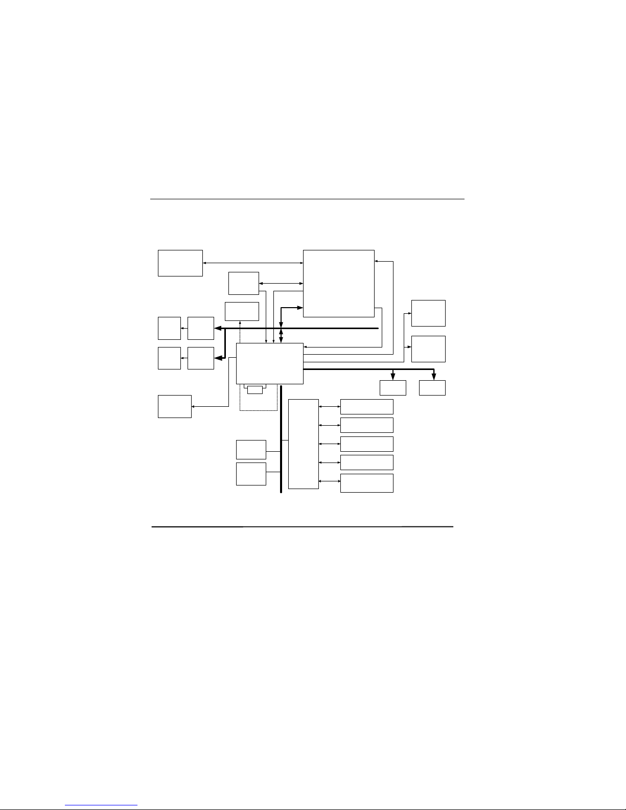
SDRAM
1 x S0-DIMM
Socket
RAM YUV Port
Por ( Video )
MediaGX
TM
MMX-TMEnhanced
Processor
Serial
Packet
RGB Port
( Graphics )
MD [ 63:0 ]
Clocks
10/100M
Ethernet
CX5530
I/O Companion
System
Clocks
CN12
USB
( 2 Ports )
CN17
RJ45
14.31818
MHz Crystal
WDT
Super I/O
83977
Winbond
CN2
FDD
FDD
Printer
COM2
COM1
CN6
RS-232
CN5
RS-232
CN7
Printer
CN16
VGA
CRT
Graphics Data
Analog Rgb
Video Data
IDE Control
ISA Bus
WAFER-5823 Block diagram
PCI Bus
CN10
IDE1
Award
BIOS
2Mb
CN11
CFA(II)
CN18
RJ45
10/100M
Ethernet
CN1
Keyboard/mouse
PS2
CN19
VGA
LCD
Chapter 2. Installation
This chapter gives instructions on how to setup and configure
WAFER-5823 board, including directions on how to set jumpers
as well as connecting peripherals, switches and indicators.
Before installation, please pay attention to the unpacking
precautions on the following page to ensure safety.
2.1 WAFER-5823 Block Diagram & Board
Layout
11
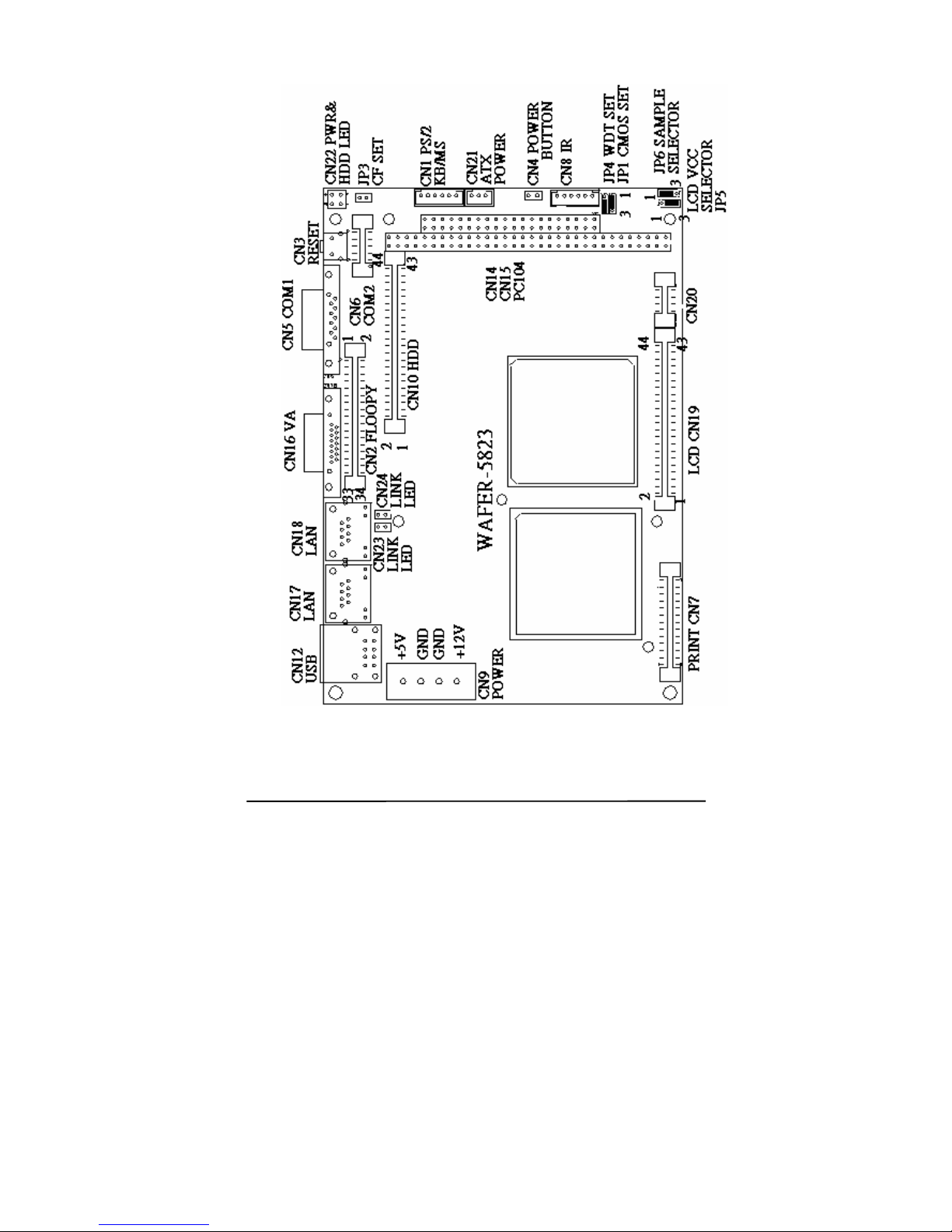
WAFER-5823 Board Jumper Setting
12
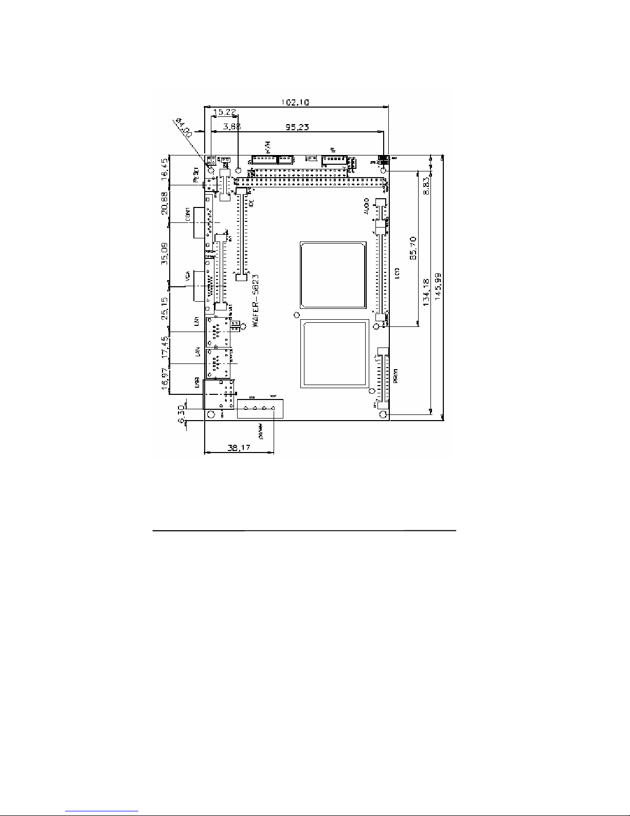
WAFER-5823 Board Dimensions

13
2.2 Unpacking Precautions
Some components of WAFER-5823 SBC are very sensitive to
static electric charges and can be damaged by a sudden rush of
power. To protect it from unintended damage, please be sure to
pay attention to these following precautions:
1. Ground yourself to remove any static charge before
touching the WAFER-5823 SBC. You can do it by using a
grounded wrist strap at all times or by frequently touching
any conducting materials that is connected to the ground.
2. Handle your WAFER-5823 SBC by its edges. Don’t touch IC
chips, leads or circuitry if not necessary.
3. Do not plug any connector or jumper while the power is
on.
2.3 System Memory DRAM
There is one 144-pin SO-DIMM socket that supports 3.3V
non-buffered SDRAM. Maximum memory size is 512MB.
2.4 Watch-Dog Timer Setting
Reading port 443H enables the Watchdog Timer. It should be
triggered before the time-out period ends, otherwise it will
assume the program operation is abnormal and will issue a
reset signal to start again. Reading port 043/843H disables the
Watchdog Timer. Refer to Appendix A for detailed information
14
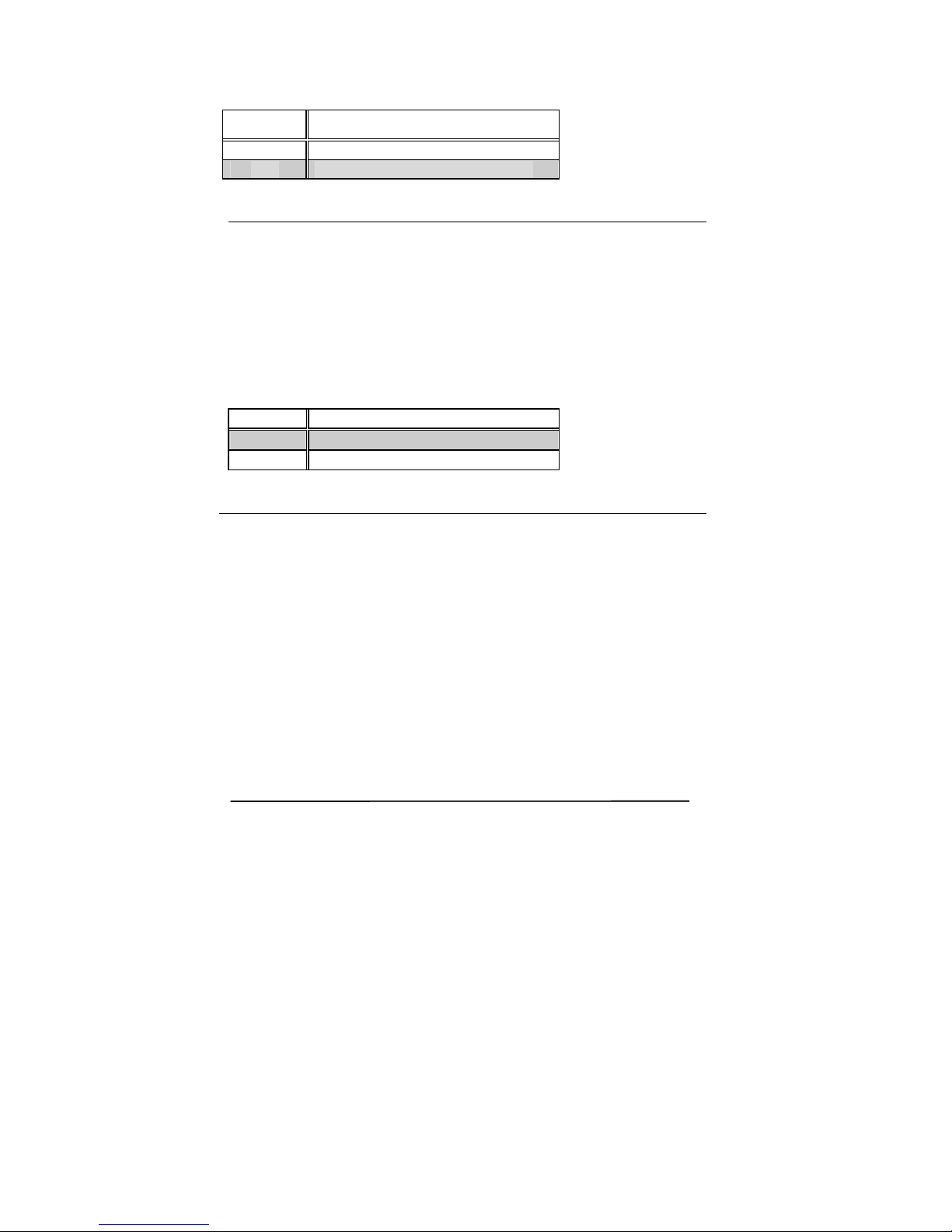
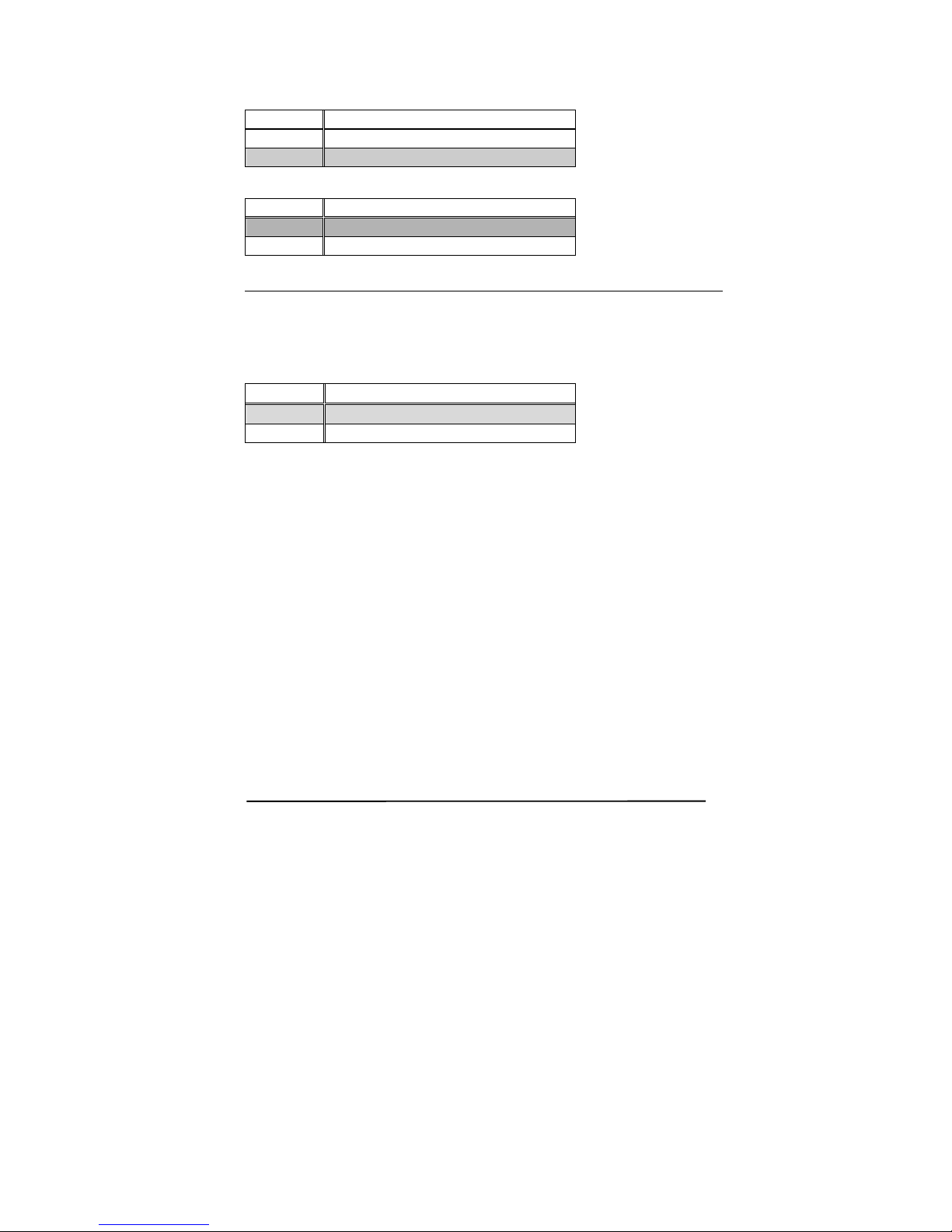
• JP4: Watchdog Active Type Setting
JP4
DESCRIPTION
1-2 DISABLED WDT
2-3 RESET WHEN WDT TIME-OUT
2.5 Clear CMOS Setup
If you need to clear the CMOS Setup (For example, you have
forgotten the password. Then what you should do is to clear
setup and reset the password.), you should close the JP1 for
about 3 seconds then open it again. Opening JP1 can set
system back to normal operation mode.
• JP1: Clear CMOS Set up (Reserve Function)
JP1 DESCRIPTION
1-2
Normal Operation
2-3
Clear CMOS Setup
2.6 LCD VCC Voltage /Panel Shift Clock
Selector
The LCD interface connector JP5 can provide 5V or 3.3V power
supply by selecting the JP5 to meet the different LCD
requirement.
The Panel Shift Clock Selector interface connector JP6 can
provide are sampled on the rising edge or falling edge by any
different LCD requirement.
15
JP5: LCD VCC Voltage Selector
JP5 DESCRIPTION
1-2 5V
2-3 3.3V
JP6: Panel Shift Clock Selector
JP6 DESCRIPTION
1-2 Rising edge sampling
2-3 Falling edge sampling
2.7 Compact Flash Setting
Set the operating mode of CompactFlash disk. This is similar to
the operation of hard disk.
JP3 DESCRIPTION
OPEN SLAVE
SHORT MASTER
 Loading...