

Page 1

WAFER-4826EV Series
User Manual
Version 1.0
STPC-DX2 133 with LCD/CRT & Ethernet
PCB Version 1.0
March 11, 2004
©Copyright 2004 by ICP Electronics Inc. All Rights Reserved
Page 2

Copyright Notice
The information in this document is subject to change without prior notice in
order to improve reliability, design and function and does not represent a
commitment on the part of the manufacturer.
In no event will the manufacturer be liable for direct, indirect, special, incidental,
or consequential damages arising from the use of the product or the inability to
use the product or documentation, even if advised of the possibility of such
damages.
This document contains proprietary information protected by copyright. All rights
reserved. No part of this manual may be reproduced in mechanical, electronic or
any other form in any means without prior written permission of the
manufacturer.
Trademarks
WAFER-4826EV is a registered trademark of ICP Electronics Inc., IBM PC is a
registered trademark of International Business Machines Corporation. Intel is a
registered trademark of Intel Corporation. AMI is a registered trademark of
American Megatrends Inc., AWARD is a registered trademark of AWARD
SOFTWARE INTERNATIONAL, Inc., Other product names mentioned in this
manual are used for identification purposes only and may be trademarks and/or
registered trademarks of their respective owners.
1
Page 3

Table of Contents
CHAPTER 1 INTRODUCTION ....................................................................4
1.1 S
1.2 P
PECIFICATIONS ..................................................................................5
ACKAGE CONTENTS..............................................................................6
CHAPTER 2 INSTALLATION......................................................................7
2.1 B
2.2 U
2.3 C
2.4 COM2 M
2.5 COM2 P
2.6 E
2.7 C
2.8 TFT LCD S
OARD LAYOUT & DIMENSIONS.................................................................7
NPACKING PRECAUTIONS .......................................................................8
OMPACT FLASH SETTINGS (JP1) ..............................................................8
ODE SETTINGS (JP2, JP3, JP4, JP6)..............................................9
IN 8 RI SETTINGS (JP7)..............................................................9
XTERNAL SWITCHES AND INDICATORS (JP5) ................................................9
LEAR CMOS SETUP (JP8)...................................................................10
ETTINGS (JP9).................................................................... 10
CHAPTER 3 CONNECTORS......................................................................11
3.1 VGA C
3.2 SO-DIMM S
3.3 LCD P
ONNECTOR (P4)........................................................................11
OCKET CONNECTOR (CN3) .................................................... 12
ANEL CONNECTOR 2.0MM 50 PIN (CN15).......................................... 13
3.4 I2C C
3.5 PC/104 C
3.6 P
3.7 S
3.8 USB P
3.9 DIO P
3.10 LAN LED C
3.11 E
3.12 F
3.13 E
3.14 12V
3.15 E
3.16 IDE D
3.17 C
ONNECTION (CN4)...................................................................... 13
ONNECTION BUS (CN5, CN6) ...................................................14
ARALLEL PORT CONNECTOR (CN10)........................................................ 15
ERIAL PORT CONNECTORS (CN7, 11, 14)................................................ 15
ORT CONNECTOR (CN12)............................................................. 16
ORT CONNECTOR (CN16) .............................................................16
ONNECTOR (CN19) ............................................................ 17
XTERNAL KEYBOARD CONNECTOR (CN13) ...............................................17
LOPPY DISK DRIVE CONNECTOR (CN8) ..................................................18
XTERNAL POWER CONNECTOR (CN1).....................................................18
OR 5V CONNECTOR (CN2)............................................................19
XTERNAL BATTERY CONNECTOR (CN9) ...................................................19
ISK DRIVE CONNECTOR (IDE1)..................................................... 19
OMPACT FLASH CARD CONNECTOR (CF1)................................................ 20
CHAPTER 4 AWARD BIOS SETUP ...........................................................21
4.1 G
ETTING STARTED .............................................................................. 21
4.2 M
AIN MENU...................................................................................... 22
2
Page 4

4.3 S
4.4
TANDARD CMOS FEATURES .................................................................24
ADVANCED BIOS FEATURES...................................................................27
4.5 A
4.6 I
4.7 P
4.8 P
4.9 L
4.10 L
4.11 S
4.12 S
4.13 E
DVANCED CHIPSET FEATURES................................................................ 30
NTEGRATED PERIPHERALS..................................................................... 30
OWER MANAGEMENT SETUP ..................................................................32
NP/PCI CONFIGURATIONS ................................................................... 34
OAD FAIL-SAFE DEFAULTS....................................................................36
OAD OPTIMIZED DEFAULTS .................................................................37
ET PASSWORD ...............................................................................37
AVE & EXIT SETUP ..........................................................................39
XIT WITHOUT SAVING....................................................................... 40
APPENDIX A. WATCHDOG TIMER...........................................................41
APPENDIX B: THE E2 KEY™ FUNCTION..................................................43
APPENDIX C I/O INFORMATION ...........................................................44
3
Page 5

Chapter 1 Introduction
Thank you for choosing the WAFER-4826EV SERIES STPC-DX2 133 CPU Board.
The WAFER-4826EV SERIES Board (denoted as WAFER-4826EV in other parts of
the manual) is an all-in-one CPU board with PC/104 for space-limited applications.
It provides all the functionalities of a full-fledged comput er.
In addition, the WAFER-4826EV provides a VGA & LCD display controller on board,
which can support CRT/LCD resolutions up to 1024x768@64K colors.
This board has a built-in Compact Flash Interface for embedded applications. The
CF is a 100% software compatible hard disk. Users can use any DOS command
without any additional software utilities.
4
Page 6

1.1 Specifications
CPU
System bus connector
System memory
Enhanced IDE
Floppy disk drive
interface
Serial ports
Bi-directional parallel
port
IrDA port
Watch-dog timer
VGA display interface
CF Interface
Keyboard / Mouse
connector
Power consumption
Embedded SGS Thomson STPC-DX2 133
PC/104 connector
Onboard SDRAM or one SO-DIMM socket, supports up to
128MB SDRAM
Supports one EIDE devices with BIOS auto-detection
capabilities
Supports up to two floppy disk drives
Four RS-232 ports with 16C550 UART (or compatible) with
16-byte FIFO buffer. Support up to 115.2Kbps. Ports can
be independently configured as COM1 or COM2.
Configurable to LPT1, LPT2, LPT3 or disabled. Supports
EPP/ECP/SPP.
Supports Infrared (IrDA) interface (Reserved/optional)
Can be set by 1-255 seconds intervals. Reset is triggered
when CPU does not periodically trigger the timer.
Complete backward compatibility to VGA and SVGA,
supports resolution up to 1024 x 768 @ 64K colors.
One CF card with BIOS auto-detection capabilities.
Supports standard PC/AT keyboards and PS/2 mice
+5V @ 2.6A
Operating temperature
0° - 60° C (CPU requires a fan to use in environments
above 60°C)
5
Page 7

1.2 Package Contents
The WAFER-4826EV package includes the following items:
WAFER-4826EV CPU board
1 Driver/Software CD
3 RS-2323 cables
1 Printer Cable
1 FDD cable
1 HDD cable
One 6-pin head which converts to two 6-pin DIN cable for keyboard and
mouse connection (Y Cable) x 1
User Manual
If any of these items is missing or damaged, please contact the dealer where the
product was purchased. Keep the shipping materials and carton in case you want
to ship or store the product in the future.
6
Page 8

Chapter 2 Installation
This chapter describes how to install the WAFER-4826EV. Read the unpacking
information carefully and refer to the layout diagram of WAFER-4826EV below
whenever necessary.
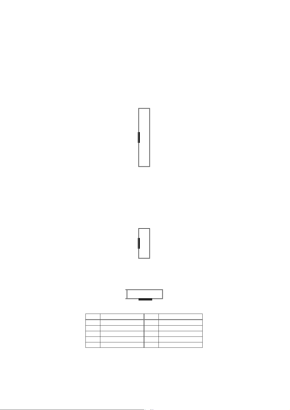
2.1 Board Layout & Dimensions
7
Page 9

2.2 Unpacking Precautions
Some components on WAFER-4826EV SBC are very sensitive to static and can be
damaged by a sudden power surge. To protect it from unintentional damage,
please be sure to follow these precautions:
Ground yourself to remove any static charge before touching WAFER-4826EV
SBC. You can do it by using an anti-static wrist strap connected to the
ground or by frequently touching any grounded conducting materials.
Handle your WAFER-4826EV SBC by its edges. Do not touch IC chips, leads
or circuitry as far as possible.
Do not plug in any connectors or set any jumpers when the power is on.
2.3 Compact Flash Mode Setting (JP1)
The Compact Flash on the WAFER-4826EV is Type II, and it uses IDE2.
JP1: Master/Slave Mode Settings
2 4 6
1 3 5
JP1 (1-2) DESCRIPTION
SHORT MASTER
OPEN SLAVE
8
Page 10

2.4 COM2 Mode setting (JP2, JP3, JP4, JP6)
JP2, JP3, JP4, JP6: COM2 RS-232 or RS-422/485 Mode Selections
JP3
2 4 6
1 3 5
JP4
2 4 6
1 3 5
JP2
1 2 3
JP6
2 4
1 3
JP2 JP3 & JP4 DESCRIPTION
1-2 short 1-3 & 2-4 short RS-422/485
2-3 short * 3-5 & 4-6 short RS-232
JP6 DESCRIPTION
OPEN RS-422
1-3 & 2-4 short * RS-485
Note: If using RS422/485, the COM2 on the main board will be disabled.
2.5 COM2 Pin 8 RI Settings (JP7)
JP7: Pin 8 RI Settings
JP7
2 4 6
1 3 5
JP7 CN7 PIN 8
3-5, 4-6 Short * RI
3-5, 2-4 Short +5V
1-3, 2-4 Short +12V
2.6 External Switches and Indicators (JP5)
There are several external switches and indicators for monitoring and controlling
your CPU board. All functions are contained in the JP5 connector.
9
Page 11

JP5: Pin Assignment and Functions
15 .. .. 5 3 1
16 .. .. 6 4 2
FUNCTION PIN DESCRIPTION
1 Battery + Ext. Battery
3 GND
5 GND RESET
7 RESET
9 +5V HDD LED
11 IDE_LED 13 Buzzer - SPEAKER
15 SPK SIGNAL
Reserved
(IrDA port)
(KEYLOCK)
2 +5V
4 Rev. (FIR-RX)
6 IR-RX
8 GND
10 IR-TX
12 CIR-RX
14 Rev. (KEYLOCK) Reserved
16 GND
Jump
for
Buzzer
2.7 Clear CMOS Setup (JP8)
If you want to clear the CMOS, for example, you forgot the your password, you
should clear the CMOS and reset the password, you should short JP8 (1-2) for
about 3 seconds. The password will be cleared from the CMOS.
JP8: Clear CMOS Setup (Reserved Function)
1 2 3
JP8 DESCRIPTION
2-3 NORMAL
1-2 CLEAR CMOS
2.8 TFT LCD Settings (JP9)
JP9: TFT LCD type (5V / 3V & FPCLK / #FPCLK) Settings
2 4 6
1 3 5
JP9 DESCRIPTION
2 – 4 5V TFT LCD
4 – 6 3V TFT LCD
1 – 3 #FPCLK
3 – 5 FPCLK
10
Page 12

Chapter 3 Connectors
This chapter describes how to connect peripherals, switches and indicators to the
WAFER-4826EV board.
Table of Connectors
LABEL FUNCTION
P1 COM1 Connector
P2 External USB Connector (rev)
P3 PS/2 Mouse and Keyboard Connector
P4 VGA Connector
P5 Ethernet Connector
CN1 External Power Connector
CN2 12V or 5V(rev) Connector (for FAN etc.)
CN3 SO-DIMM Socket Connector
CN4 I2C Connector (rev)
CN5 PC/104-64 CON A
CN6 PC/104-40 CON B
CN7 COM2 Connector (RS-232/422/485)
CN8 Floppy Disk Drive Connector
CN9 External Battery Connector
CN10 Parallel Port Connector
CN11 COM3 Connector
CN12 USB Connector
CN13 External Keyboard Connector
CN14 COM4 Connector
CN15 LCD Panel Connector
CN16 DIO Connector
CN17 COM5 Connector
CN18 COM6 Connector
CN19 LAN LED Connector
IDE1 IDE Disk Drive Connector
CF1 Compact Flash Card Connector
3.1 VGA Connector (P4)
The built-in DB15 VGA connector of WAFER-4826EV can be directly connected to
your CRT monitor via the attached VGA cable.
P4: DB15 VGA Connector
PIN DESCRIPTION PIN DESCRIPTION
1 RED 2 GREEN
3 BLUE 4 NC
5 GROUND 6 GROUND
7 GROUND 8 GROUND
9 5V 10 GROUND
11 NC 12 SDA
13 HSYNC 14 VSYNC
15 SCL
11
Page 13

3.2 SO-DIMM Socket Connector (CN3)
PIN DES. PIN DES. PIN DES. PIN DES.
1 GND 19 MD7 37 MD8 55 GND
2 GND 20 MD39 38 MD40 56 GND
3 MD0 21 GND 39 MD9 57 NC
4 MD32 22 GND 40 MD41 58 NC
5 MD1 23 DQ0 41 MD10 59 NC
6 MD33 24 DQ4 42 MD42 60 NC
7 MD2 25 DQ1 43 MD11 61 CLK0
8 MD34 26 DQ5 44 MD43 62 CKE0
9 MD3 27 3.3V 45 3.3V 63 3.3V
10 MD35 28 3.3V 46 3.3V 64 3.3V
11 3.3V 29 MA0 47 MD12 65 RAS#
12 3.3V 30 MA3 48 MD44 66 CAS#
13 MD4 31 MA1 49 MD13 67 WE#
14 MD36 32 MA4 50 MD45 68 CKE1
15 MD5 33 MA2 51 MD14 69 CSA#
16 MD37 34 MA5 52 MD46 70 NC
17 MD6 35 GND 53 MD15 71 CSB#
18 MD38 36 GND 54 MD47 72 NC
PIN DES. PIN DES. PIN DES. PIN DES.
73 GND 91 GND 109 MA9 127 MD27
74 CLK1 92 GND 110 BA1 128 MD59
75 GND 93 MD20 111 MA10 129 3.3V
76 GND 94 MD52 112 MA11 130 3.3V
77 NC 95 MD21 113 3.3V 131 MD28
78 NC 96 MD53 114 3.3V 132 MD60
79 NC 97 MD22 115 DQ2 133 MD29
80 NC 98 MD54 116 DQ6 134 MD61
81 3.3V 99 MD23 117 DQ3 135 MD30
82 3.3V 100 MD55 118 DQ7 136 MD62
83 MD16 101 3.3V 119 GND 137 MD31
84 MD48 102 3.3V 120 GND 138 MD63
85 MD17 103 MA6 121 MD24 139 GND
86 MD49 104 MA7 122 MD56 140 GND
87 MD18 105 MA8 123 MD25 141 SDA
88 MD50 106 BA0 124 MD57 142 SCL
89 MD19 107 GND 125 MD26 143 3.3V
90 MD51 108 GND 126 MD58 144 3.3V
12
Page 14

3.3 LCD Panel Connector 2.0mm 50Pin (CN15)
2 50
1 49
..
..
.
.. ..
PIN DESCRIPTION PIN DESCRIPTION
1 NC 2 NC
3 NC 4 NC
5 NC 6 NC
7 NC 8 NC
9 NC 10 NC
11 NC 12 NC
13 NC 14 FPD_R3
15 FPD_R5 16 FPD_R4
17 NC 18 FPD_R2
19 NC 20 FPD_R0
21 FPD_R1 22 FPD_G4
23 FPD_G3 24 FPD_G2
25 FPD_G5 26 FPD_G1
27 FPD_B5 28 FPD_G0
29 +LCD 30 +LCD
31 NC 32 NC
33 FPD_B2 34 FPD_B4
35 FPD_B1 36 FPD_B3
37 FPD_B0 38 NC
39 FPD_EN 40 NC
41 FPD_CK 42 EN_BKL
43 EN_VDD 44 FPD_VS
45 EN_VEE 46 FPD_HS
47 GND 48 GND
49 +VBL 50 +VBL
3.4 I2C Connection (CN4)
1 2 3
CN4 DESCRIPTION
1 DATA
2 CLOCK
3 GND
13
Page 15

3.5 PC/104 Connection Bus (CN5, CN6)
The WAFER-4826EV's PC/104 expansion bus lets you attach any PC/104 module.
There are two PC/104 connectors on this board: PC/104-64 and PC/104-40.
CN5: PC/104-64 CON A
2
1
CN6: PC/104-64 CON B 40
CN6: PC/104-64 CON B 13 SD2 14 -12V
PIN
DES. PIN DES. 15 SD1 16 ZWS
2 GND 1 GND 17 SD0 18 +12V
4 MCS16 3 SBHE# 19 IOCHRDY 20 GND
6 IOCS16 5 LA23 21 AEN 22 SMEMW#
8 IRQ10 7 LA22 23 LA19 24 SMEMR#
10 IRQ11 9 LA21 25 LA18 26 IOW#
12 IRQ12 11 LA20 27 LA17 28 IOR#
14 IRQ15 13 LA19 29 SA16 30 DACK3#
16 IRQ14 15 LA18 31 SA15 32 DRQ3
18 DACK0# 17 LA17 33 SA14 34 DACK1#
20 DRQ0 19 MEMR# 35 SA13 36 DRQ1
22 DACK5# 21 MEMW# 37 SA12 38 REFRESH#
24 DRQ5 23 SD8 39 SA11 40 SYSCLK
26 DACK6# 25 SD9 41 SA10 42 IRQ7
28 DRQ6 27 SD10 43 SA9 44 IRQ6
30 DACK7# 29 SD11 45 SA8 46 IRQ5
32 DRQ7 31 SD12 47 SA7 48 IRQ4
34 +5V 33 SD13 49 SA6 50 IRQ3
36 MASTER# 35 SD14 51 SA5 52 DACK2
38 GND 37 SD15 53 SA4 54 TC
40 GND 39 NC 55 SA3 56 ALE
1
2
CN5: PC/104-64 CON A
PIN DES. PIN
1 IOCHCK# 2 GND
3 SD7 4 RSTDRV
5 SD6 6 +5V
7 SD5 8 IRQ9
9 SD4 10 -5V
11 SD3 12 DRQ2
57 SA2 58 +5V
59 SA1 60 OSC
61 SA0 62 GND
63 GND 64 GND
64
DES.
14
Page 16
3.6 Parallel Port Connector (CN10)
This port is usually connected to a printer. WAFER-4826EV includes an on-board
parallel port to be accessed through a 26-pin mini-pitched flat-cable connector
CN10.
CN10: 26-PIN Female Connector
1
STB#
DATA 0
DATA 1
DATA 2
DATA 3
DATA 4
DATA 5
DATA 6
DATA 7
ACK#
BUSY
PE
SLCT#
25
2
AFD#
ERROR#
INIT#
SLIN#
GND
GND
GND
GND
GND
GND
GND
GND
NC
26
3.7 Serial Port Connectors (CN7, CN11, CN14)
The WAFER-4826EV offers two high-speed NS16C550 compatible 16-byte serial
Read/Receive UART FIFO ports.
CN11, CN14: (COM3, COM4) 10-PIN Female Connector
1
DCD#
RXD
TXD
DTR#
GND
9
CN7: (COM2) 10-PIN Female Connector
2 10
1 9
PIN DESCRIPTION PIN DESCRIPTION
1 TX- / DCD# 2 DSR#
3 TX+ / RXD 4 RTS#
5 RX+ / TXD 6 CTS#
7 RX- / DTR# 8 RI#/5V/12V
9 GND 10 NC
2
10
DSR#
RTS#
CTS#
RI#
NC
15
Page 17

3.8 USB Port Connector (CN12)
2 8
1 7
CN12 DESCRIPTION
1 +5V
2 GND
3 P0D4 P1D+
5 P0D+
6 P1D7 GND
8 +5V
3.9 DIO Port Connector (CN16)
This port is connected to DIO 0 to 7; all pins can be set as input or output.
IO port DESCRIPTION
Direction Register
320 (hex)
326 (hex)
DIO 0 (bit0) ~ DIO 7 (bit7)
1=input; 0=Output
DIO Port
DIO 0 (bit0) ~ DIO 7 (bit7)
2 10
1 9
CN16 DESCRIPTION
1 GND
2 +5V
3 DIO 7
4 DIO 6
5 DIO 5
6 DIO 4
7 DIO 3
8 DIO 2
9 DIO 1
10 DIO 0
16
Page 18

3.10 LAN LED Connector (CN19)
2 4
1 3
CN19 DESCRIPTION
1 LINK-
2 LINK+
3 ACT4 ACT+
3.11 External Keyboard Connector (CN13)
The included 5 or 6-pin plug will convert to two 6-pin DIN cables for keyboard
(mouse) connection enables users to connect PS/2 keyboard (and mouse).
Simply connect your keyboards and mice to the attached cable to use them as
you normally would.
CN13 : PS/2 Keyboard (mouse/rev) Connector
6 1
CN13 DESCRIPTION
1 KEYBOARD CLOCK
2 KEYBOARD DATA
3 NC. (Rev. MOUSE CLOCK)
4 GND
5 SV
6 NC. (Rev. MOUSE DATA)
17
Page 19

3.12 Floppy Disk Drive Connector (CN8)
The WAFER-4826EV board is equipped with a 34-pin daisy-chain drive connector
cable which supports up to two floppy drives. The detailed pin assignments of the
connector is described as below:
2 34
1 33
PIN DESCRIPTION PIN DESCRIPTION
1 GND 2 REDUCE WRITE
3 GND 4 NC
5 GND 6 NC
7 NC 8 INDEX#
9 GND 10 MOTOR ENABLE A#
11 GND 12 DRIVE SELECT B#
13 NC 14 DRIVE SELECT A#
15 GND 16 MOTOR ENABLE B#
17 GND 18 DIRECTION#
19 GND 20 STEP#
21 GND 22 WRITE DATA#
23 GND 24 WRITE GATE#
25 GND 26 TRACK 0#
27 GND 28 WRITE PROTECT#
29 NC 30 READ DATA#
31 GND 32 SIDE 1 SELECT#
33 NC 34 DISK CHANGE#
3.13 External Power Connector (CN1)
The WAFER-4826EV has an on-board external power connector CN1. The
WAFER-4826EV is only powered by VCC (5V), which is conducted through pin 4 of
the external power connector CN1, and power GND from pin 2 and pin 3. The
extra power supply +12V provided by CN1 will be passed to CN5 and CN6 for
PC104 slot use only.
CN1: External Power Connector
PIN DESCRIPTION
1 +12V
2 GND
3 GND
4 +5V
1 2 3 4
18
Page 20

3.14 12V or 5V Connector (CN2)
2
3
The WAFER-4826EV provides an optional fan power connector, which works only
when +12V power is supplied to CN1. Please note that a heat sink has already
been installed in STPC chip of the WAFER-4826EV. However, when running
WAFER-4826EV under a temperature of above 60℃, users will have to add an
additional CPU cooling fan.
CN2: 12V or 5V for FAN etc. connector
GND
+12V
NC(+5V)
1
3.15 External Battery Connector (CN9)
The WAFER-4826EV provides an (Molex 1.25mm 2pin) optional battery connector.
Note: If external battery is to be used, please remove the on board battery.
1
2
Battery +
GND
3.16 IDE Disk Drive Connector (IDE 1)
You can attach four IDE (Integrated Device Electronics) hard disk drives to the
WAFER-4826EV IDE controller.
IDE1: HDD Connector
1 2
RESET#
DATA 7
DATA 6
DATA 5
DATA 4
DATA 3
DATA 2
DATA 1
DATA 0
GND
DREQ
IOW#
IOR#
IORDY
IDACK#
IDE
INTERRUPT
SA1
SA0
CS0#
IDE ACTIVE#
+5V
GND
43
44
GND
DATA 8
DATA 9
DATA 10
DATA 11
DATA 12
DATA 13
DATA 14
DATA 15
NC
GND
GND
GND
GND
GND
NC
NC
SA2
CS1#
GND
+5V
NC
19
Page 21

3.17 Compact Flash Card Connector (CF1)
PIN DESCRIPTION PIN DESCRIPTION
1 GND 26 NC
2 DATA 3 27 DATA 11
3 DATA 4 28 DATA 12
4 DATA 5 29 DATA 13
5 DATA 6 30 DATA 14
6 DATA 7 31 DATA 15
7 CS0# 32 CS1#
8 NC 33 NC
9 GND 34 IOR#
10 NC 35 IOW#
11 NC 36 +5V
12 NC 37 CF INTERRUPT
13 +5V 38 +5V
14 NC 39 SEL
15 NC 40 NC
16 NC 41 RESET#
17 NC 42 IORDY
18 SA2 43 NC
19 SA1 44 +5V
20 SA0 45 CF ACTIVE#
21 DATA 0 46 NC
22 DATA 1 47 DATA 8
23 DATA 2 48 DATA 9
24 NC 49 DATA 10
25 NC 50 GND
20
Page 22

Chapter 4 AWARD BIOS Setup
This appendix discusses the Setup program built into the BIOS. The Setup
program enables users to configure the system. This configuration is then stored
in battery-backed CMOS RAM so that it retains the Setup information while the
power is off.
4.1 Getting Started
The BIOS is immediately active when you turn on the computer. While the BIOS
is in control, the CMOS Setup program can be activated in one of two ways:
1. By pressing <Del> immediately after switching the system on, or
2. By pressing the <Del> key when the following message appears briefly at the
bottom of the screen during the POST (Power On Self-Test).
Press DEL to enter SETUP
If the message disappears before you respond and you still wish to enter Setup,
restart the system to try again by turning it OFF then ON or pressing the "RESET"
button on the system case. You may also restart by simultaneously pressing
<Ctrl>, <Alt>, and <Delete> keys. If you do not press the keys at the correct
time and the system does not boot, an error message will be displayed and you
will again be asked to...
PRESS F1 TO CONTINUE, DEL TO ENTER SETUP
In general, you can use the arrow keys to highlight items, press <Enter> to
select, use the Page Up and Page Down keys to change entries, press <F1> for
help and press <Esc> to quit. The table on the next page provides more details
about how to navigate in the Setup program using the keyboard.
21
Page 23

KEY FUNCTION
Up Arrow Move to the previous item
Down Arrow Move to the next item
Left Arrow Move to the item on the left (menu bar)
Right Arrow Move to the item on the right (menu bar)
Esc Main Menu: Quit without saving changes
Submenus: Exit Current page to the next
higher level menu
Move Enter Move to the item you desired
Page Up key Increase the numeric value or make changes
Page Down key Decrease the numeric value or make changes
+ key Increase the numeric value or make changes
- key Decrease the numeric value or make changes
Esc Key Main Menu- Quit an d not save changes into
CMOS
Status Page Setup Menu and Option Page Setup
Menu- Exit current page and return to Main
Menu
F1 key General help on Setup navigation keys
F5 key Load previous values from CMOS
F6 key Load the fail-safe defaults from BIOS default
table
F7 key Load the optimized defaults
F10 key
ave all the CMOS changes and exit
4.2 Main Menu
Once you enter the AwardBIOS™ CMOS Setup Utility, the Main Menu will appear
on the screen. The Main Menu allows you to select from several setup functions
and two exit choices. Use the arrow keys to select among the items and press
<Enter> to accept and enter the sub-menu.
Phoenix - AwardBIOS CMOS Setup Utility
► Standard CMOS Features
► Advanced BIOS Features
► Advanced Chipset Features
► Integrated Peripherals
► Power Management Setup
► PnP/PCI Configurations
Esc : Quit F9 : Menu in BIOS ↑ ↓ ← → : Select Item
F10 : Save & Exit Setup
► Load Fail-Safe Defaults
► Load Optimized Defaults
► Set Password
► Save & Exit Setup
► Exit Without Saving
Time, Date, Hard Disk Type...
22
Page 24

Note that a brief description of each highlighted selection appears at the bottom
of the screen.
The main menu includes the following main setup categories. Please note that
some systems may not include all entries.
Standard CMOS Features
Select this item for basic system configuration. See Section 4.3 for the
details.
Advanced BIOS Features
Select this item menu to set the Advanced Features available on your system.
See Section 4.4 for the details.
Advanced Chipset Features
Select this item to change the values in the chipset registers an d optimize
your system's performance. See section 4.5 for the details.
Integrated Peripherals
Select this item to specify your settings for integrated peripherals. See
section 4.6 for the details.
Power Management Setup
Select this item to specify your settings for power management. See section
4.7 for the details
PnP / PCI Configurations
This entry appears if your system supports PnP / PCI. See section 4.8 for
the details.
Load Fail-Safe Defaults
Select this item to load the BIOS default values for the minimal/stable
performance for your system to operate. See section 4.9 for the details.
Load Optimized Defaults
Select this item to load the BIOS default values that are factory settings for
optimal performance system operations. While Award has designed the
custom BIOS to maximize performance, the factory has the right to change
these defaults to meet their needs. See section 4.10 for the details.
Set Password
Select this item to set Passwords. See section 4.11 for the detail.
Save & Exit Setup
Saves CMOS value changes to CMOS and exit setup. See section 4.12 for
the details.
Exit Without Save
Abandons all CMOS changes and exit setup. See section 4.13 for the details.
23
Page 25

4.3 Standard CMOS Features
The items in Standard CMOS Setup Menu are divided into 10 categories. Each
category includes zero, one or more setup items. Use the arrow keys to highlight
the item and then use the <Page Up> or <Page Down> keys to select the value
for each item.
Phoenix - AwardBIOS CMOS Setup Utility
Standard CMOS Features
Date (mm:dd:yy) Tue, Feb 25 2003
Time (hh:mm:ss) 17 : 20 : 10
► IDE Primary Master
► IDE Primary Slave
► IDE Primary Master
► IDE Primary Slave
Drive A [1.44M, 3.5 in.]
Drive B [None]
LCD&CRT [Both]
Panel Type [640x480 18-TFT]
Halt On [All , But Keyboard]
Base Memory 640K
Extended Memory 64512K
Total Memory 65536K
↑↓→←:Move Enter:Select +/-/PU/PD:Value F10:Save ESE:Exit F1:General Help
F5: Previous Values F6: Fail-Safe Defaults F7:Optimized Defaults
Menu Level ►
Change the day, month,
year and century
Item Help
24
Page 26

Main Menu Selections
ITEM OPTIONS DESCRIPTION
Date MM DD YYYY Set the system date.
Time HH : MM : SS Set the system time
IDE Primary Options are in its sub
IDE Primary Slave Options are in its sub
IDE Secondary Options are in its sub
IDE
Secondary Slave
Drive A
Drive B
CRT&LCD BOTH
Halt On All Errors
Base Memory N/A Displays the amount of
Extended Memory N/A Displays the amount of
Total Memory N/A Displays the total memory
menu
(described in Table 3)
menu
(described in Table 3)
menu
(described in Table 3)
Options are in its sub
menu
(described in Table 3)
None
360K, 5.25 in
1.2M, 5.25 in
720K, 3.5 in
1.44M, 3.5 in
2.88M, 3.5 in
LCD
CRT
No Errors
All, but Keyboard
All, but Diskette
All, but Disk/Key
Press <Enter> to enter the
sub menu of detailed options
Press <Enter> to enter the
sub menu of detailed options
Press <Enter> to enter the
sub menu of detailed options
Press <Enter> to enter the
sub menu of detailed options
Select the type of floppy disk
drive installed in your system
Select the default video device
Select the situation in which
you want the BIOS to stop the
POST process and notify you
conventional memory
detected during boot up
extended memory detected
during boot up
available in the system
25
Page 27

IDE Adapters
The IDE adapters control the hard disk drive. A separate sub menu is used to
configure each hard disk drive.
The IDE primary master sub menu is displayed like the following:
Phoenix - AwardBIOS CMOS Setup Utility
IDE Primary Slave
IDE HDD Auto-Detection [Press Enter]
IDE Primary Slave [Auto]
Access Mode [Auto]
Capacity
Cylinder 0 MB
Head 0
Precomp 0
Landing Zone 0
Sector 0
↑↓→←:Move Enter:Select +/-/PU/PD:Value F10:Save ESE:Exit
F1:General Help
F5: Previous Values F6: Fail-Safe Defaults F7:Optimized Defaults
Menu Level ►
Change the day, month,
year and century
Item Help
Use the keys shown at the bottom of the screen to navigate the options and to
exit to the main menu. Refer to the table below to configure the hard disks.
ITEM OPTIONS DESCRIPTION
IDE HDD Auto-detection Press Enter Press Enter to auto-detect the HDD on
this channel. If detection is successful,
it fills the remaining fields on this menu.
IDE
Primary Master
None
Auto
Manual
Capacity Auto Display
your disk
drive size
Access Mode CHS
LBA
Large
Auto
The following are available only if the ‘IDE Primary Master’ item is set to ‘Manual’
Cylinder Min = 0
Max = 65535
Head Min = 0
Max = 255
Precomp Min = 0
Max = 65535
Landing zone Min = 0
Max = 65535
Sector Min = 0
Max = 255
Selecting ‘manual’ lets you set the
remaining fields on this screen. Selects
the type of fixed disk. "User Type" will
let you select the number of cylinders,
heads, etc. Note: PRECOMP=65535
means no hard disk!
Disk drive capacity (Approximated).
Note that this size is usually slightly
greater than the size of a formatted disk
given by a disk-checking program.
Choose the access mode for this hard
disk
Set the number of cylinders for this
hard disk.
Set the number of read/write heads
**** Warning: Setting a value of
65535 means no hard disk
****
Number of sectors per track
26
Page 28

4.4 Advanced BIOS Features
Advanced BIOS features enable the configuration of the basic system operation
with the options to select system’s default speed, boot sequence, keyboard
options, shadowing and security.
Phoenix - AwardBIOS CMOS Setup Utility
Advanced BIOS Features
Virus Warning [Disabled]
CPU Internal Cache [Enabled]
Quick Power On Self Test [Enabled]
First Boot Device [Floppy]
Second Boot Device [SCSI]
Third Boot Device [HDD-0]
Boot Other Device [Enabled]
Swap Floppy Drive [Disabled]
Boot Up Floppy Seek [Enabled]
Boot Up NumLock Status [On]
Boot Up System Speed [High]
Gate A20 Option [Fast]
Typematic Rate Setting [Disabled]
Typemtaic Rate (Chars/Sec) 6
Typematic Delay (Msec) 250
Security Option [Steup]
OS Select For DRAM > 64MB [Non-OS2]
Video BIOS Shadow [Enabled]
C8000-CBFFF Shadow [Disabled]
↑↓→←:Move Enter:Select +/-/PU/PD:Value F10:Save ESE:Exit
F1:General Help F5: Previous Values F6: Fail-Safe Defaults
F7:Optimized Defaults
Menu Level ►
Allows you to choose
the VIRUS warning
feature for IDE Hard
Disk boot sector
protection. If this
function is enabled
and someone attempts to
write data into this
area, BIOS will show
a warning message on
screen and the alarm will
beep.
Phoenix - AwardBIOS CMOS Setup Utility
Advanced BIOS Features
CC000-CFFFF Shadow [Disabled]
D0000-D3FFF Shadow [Disabled]
D4C00-D7FFF Shadow [Disabled]
D8000-DBFFF Shadow [Disabled]
DC000-DFFFF Shadow [Disabled]
Small Logo(EPA) Show [Disabled]
Menu Level ►
Item Help
Item Help
↑↓→←:Move Enter:Select +/-/PU/PD:Value F10:Save ESE:Exit
F1:General Help F5: Previous Values F6: Fail-Safe Defaults
F7:Optimized Defaults
27
Page 29

Virus Warning
Enables the selection of VIRUS Warning feature for the IDE Hard Disk boot
sector protection. When this function is enabled and when a write is
attempted in the hard disk boot sector, BIOS will show a warning message
on the screen and the alarm will beep. The options are listed below:
OPTION DESCRIPTION
Enabled Activates automatically when the syste m boots up causing a
warning message to appear when anything attempts to
access the boot sector or hard disk partition table.
Disabled No warning message will appear when anything attempts to
access the boot sector or hard disk partition table.
CPU Internal Cache
This attempts to speed up memory access. The amount of speedup is
dependant on the CPU/chipset design.
Options: Enabled, Disabled.
Quick Power On Self-Test
This category speeds up the Power On Self Test (POST) after you turn on the
computer. If it is enabled, the BIOS will shorten or skip some tests during
POST.
Options: Enabled, Disabled.
First/Second/Third/Other Boot Device
The BIOS will attempt to load the operating system from the devices in the
sequence selected in these items.
Options: Floppy, LS120, HDD0-3, SCSI, CDROM, ZIP100, LAN, and Disabled.
Swap Floppy Drive
If the system has two floppy drives, you can swap the logical drive name
assignments.
Options: Enabled, Disabled.
Boot Up Floppy Seek
Checks the floppy disk drives for an operating system during boot up.
Disabling this option speeds the startup of the computer.
Options: Enabled, Disabled.
Boot Up NumLock Status
Choose whether to engage NumLock upon turning the computer on.
Options: On, Off.
28
Page 30

Gate A20 Option
Choose whether the chipset or the keyboard controller should control
GateA20.
OPTION DESCRIPTION
Normal A pin in the keyboard controller controls GateA20
Fast Allows the chipset to take over control of the GateA20
Typematic Rate Setting
Keystrokes repeat (typematic) at a rate determined by the keyboard
controller. When enabled, the typematic rate and typematic delay can be
selected.
Options: Enabled, Disabled.
Typematic Rate (Chars/Sec)
Sets the number of times a second to repeat a keystroke when you hold the
key down.
Options: 6, 8, 10, 12, 15, 20, 24, and 30.
Typematic Delay (Msec)
Sets the delay time after the key is held down before it begins to repeat the
keystroke.
Options: 250, 500, 750, and 1000.
Security Option
Select whether the password is required every time the system boots or only
when you enter setup.
OPTION DESCRIPTION
System The system will not boot and access to Setup will be denied
if the correct password is not entered at the prompt.
Setup The system will boot, but access to Setup will be denied if
the correct password is not entered at the prompt.
Note: To disable security, select PASSWORD SETTING at Main Menu and
you will be asked to enter a password. Do not type anything and
Press <Enter> to disable security. Once the security is disabled, you
can start up the system and enter BIOS setup without using a
password.
OS Select For DRAM > 64MB
If the system has more than 64MB of RAM, select OS2 if OS/2 is used on the
computer. Otherwise, select Non-OS2.
Options: Non-OS2, OS2.
29
Page 31

Video BIOS Cacheable
Enabling this option will enable caching of the video BIOS, which results in
better system performance. However, if any program writes to this memory
area, a system error may result.
Options: Enabled, Disabled.
4.5 Advanced Chipset Features
Use this menu to specify your settings for ISA/SDRAM frequency controls.
Phoenix - AwardBIOS CMOS Setup Utility
Advanced Chipset Features
Memory Hole (15M –16M) [Disabled]
ISA Clcck [14.3MHz/2]
SDRAM Clock [ 66MHz]
DRAM_Write_Posting [Disabled]
Item Help
Menu Level ►
↑↓→←:Move Enter:Select +/-/PU/PD:Value F10:Save ESE:Exit
F1:General Help F5: Previous Values F6: Fail-Safe Defaults
F7:Optimized Defaults
4.6 Integrated Peripherals
Use this menu to specify your settings for integrated peripherals.
Phoenix - AwardBIOS CMOS Setup Utility
Integrated Peripherals
On-Chip Local Bus IDE [Enabled]
IDE Buffer for DOS & Win [Enabled]
The 2nd channel IDE [Enabled]
IDE Primary Master PIO [Auto]
IDE Primary Slave PIO [Auto]
IDE Secondary Master PIO [Auto]
IDE Secondary Slave PIO [Auto]
IDE HDD Block Mode [Enabled]
KBC input clock [8 MHz]
Onboard FDC Controller [Enabled]
Onboard Serial Port 1 [3F8/IRQ4]
Onboard Serial Port 2 [2F8/IRQ3]
Onboard IR Controller
IR Address Select [3E0H]
IR Mode
IR Transmission delay [Enabled]
IR IRQ Select [IRQ10]
IR Mode Use DMA [Disabled]
Onboard Parallel Port
↑↓→←:Move Enter:Select +/-/PU/PD:Value F10:Save ESE:Exit
F1:General Help
F5: Previous Values F6: Fail-Safe Defaults F7:Optimized Defaults
Item Help
Menu Level ►
30
Page 32

Phoenix - AwardBIOS CMOS Setup Utility
Integrated Peripherals
ECP Mode Use DMA [3]
EPP Mode Select [EPP1.9]
Watch Dog Timer S elect [Disabled]
↑↓→←:Move Enter:Select +/-/PU/PD:Value F10:Save ESE:Exit
F1:General Help
F5: Previous Values F6: Fail-Safe Defaults F7:Optimized Defaults
Item Help
Menu Level ►
On-Chip Local Bus IDE
The chipset contains a Local Bus IDE interface with support for two IDE
channels. Select “Enabled” to enable the primary IDE interface. Select
“Disabled” to disable this interface
Options: Enabled, Disabled.
IDE Primary/Secondary Master/Slave PIO
The four IDE PIO (Programmed Input/Output) fields let you set a PIO mode
(0-4) for each of the four IDE devices that the onboard IDE interface
supports. Modes 0 through 4 provide successively increased performance.
In Auto mode, the system automatically determines the optimal mode for
each device.
Options: Auto, Mode 0, Mode 1, Mode 2, Mode 3, and Mode 4.
IDE HDD Block Mode
Block mode is also called block transfer, multiple commands, or multiple
sector read/write. If your IDE hard drive supports block mode (most new
drives do), select “Enabled’ for automatic detection of the optimal number of
block read/writes per sector the drive can support.
Options: Enabled, Disabled
Onboard FDC Controller
Select “Enabled” if your system has a floppy disk controller (FDC) installed
on the system board and you wish to use it. If you install and-in FDC or th e
system has no floppy drive, select Disabled in this field.
Options: Enabled, Disabled.
31
Page 33

Onboard Serial Port 1/Port 2
Select an address and corresponding interrupt for the first and second serial
ports.
Options: 3F8/IRQ4, 2E8/IRQ3, 3E8/IRQ4, 2F8/IRQ3, Disabled, Auto.
Onboard Parallel Port
This item allows you to determine onboard parallel port controller I/O
address setting.
Options: 378/IRQ7, 278/IRQ5, 3BC/IRQ7, and Disabled.
Parallel Port Mode
Select an operating mode for the onboard parallel (printer) port. Select
Normal, Compatible, or SPP unless you are certain your hardware and
software both support one of the other available modes.
Options: Normal, EPP, ECP, and ECP/EPP
ECP Mode Use DMA
Select a DMA channel for the parallel port for use during ECP mode.
Options: 3, 1.
Parallel Port EPP Type
Select EPP port type 1.7 or 1.9.
Options: EPP1.7, EPP1.9
4.7 Power Management Setup
This allows you to configure your system in a way such that you can use the
computer as you normally would, while making the most efficient use of energy
Phoenix - AwardBIOS CMOS Setup Utility
Power Management Setup
Power Management [User Define]
PM Control by APM [Yes]
Video Off Option [Susp,Stby -> Off]
Video Off Method [V/H SYNC+Blank]
** PM Timers **
HDD Power Down [Disable]
Doze Time-Out [Disable]
Standby Time-Out [Disable]
Suspend Time-Out [Disable]
** PM Events **
DMA Request (DRQ) [Disable]
PCI master device (PCIM) [Disable]
Parallel I/O (PIO) [Disable]
Serial I/O (SIO) [Disable]
Keyboard (KBD) [Enable]
Floppy Disk Controller [Disable]
Hard Disk Controller [Disable]
IRQ 15 - 1 Detection [Enable]
IRQ 0 Detection [Disable]
NMI Detection [Disable]
↑↓→←:Move Enter:Select +/-/PU/PD:Value F10:Save ESE:Exit
F1:General Help
F5: Previous Values F6: Fail-Safe Defaults F7:Optimized Defaults
Item Help
Menu Level ►
32
Page 34

Power Management
This category allows you to select the type (or amount) of power saving and
is directly related to the following modes:
HDD Power Down
When enabled, the hard disk drive will power down after a specified
time of system inactivity.
Doze Mode
When enabled, the CPU clock will run at a lower frequency after a
specified time of system inactivity.
Suspend Mode
When enabled, every component on the computer, except the CPU, will
be powered down after a specified time of system inactivity.
There are four selections for Power Management, three of which have pre-defined
settings for Doze, Standby, Suspend Modes and HDD Power Down.
OPTION DESCRIPTION
Disable (default) No power management. Disables all power
saving modes.
Min. Power Saving Minimum power management. Doze Mode =
1 hr. Standby Mode = 1 hr., Suspend Mode =
1 hr., and HDD Power Down = 15 min.
Max. Power
Saving
User Defined Allow the individual settings of Doze, Standby,
Maximum power management -- ONLY
AVAILABLE FOR SL CPU’s. Doze Mode = 1
min., Standby Mode = 1 min., Suspend Mode
= 1 min., and HDD Power Down = 1 min.
Suspend Modes (between 1 min. and 1 hr. of
inactivity) and the HDD Power Down (between
1 min. to 15 min). Each setting may also be
individually disabled.
PM Control by APM
When enabled, an Advanced Power Management device will be used to
enhance the Max. Power Saving mode and stop the CPU internal clock. If
Advance Power Management (APM) is installed on your system, selecting Yes
gives better power savings.
If the Max. Power Saving is not enabled, this will be preset to No.
Options: Yes, No.
Video Off Option
When enabled, this feature allows the VGA adapter to operate in a power
saving mode.
OPTION DESCRIPTION
Always On Monitor will remain on during power saving modes.
Suspend --> Off Monitor blanked when the systems enters the Suspend mode.
All Modes --> Off Monitor blanked when the system enters any power saving mode.
33
Page 35

Video Off Method
This determines the manner in which the monitor is blanked. Please see the
table below for details on each option.
OPTION DESCRIPTION
V/H
SYNC+Blank
This selection will cause the system to turn off
the vertical and horizontal synchronization ports
and write blanks to the video buffer.
Blank Screen This option only writes blanks to the video
buffer.
DPMS Support Select this option if your monitor supports the
Display Power Management Signaling (DPMS)
standard of the Video Electronics Standards to
select video power management settings.
4.8 PnP/PCI Configurations
This section describes configuring the PCI bus system. PCI, or Personal
Computer Interconnect, is a system which allows I/O devices to operate at
speeds nearing the speed the CPU itself, uses when communicating with its own
special components. This section covers some very technical items and it is
strongly recommended that only experienced users make any changes to the
default settings.
Phoenix - AwardBIOS CMOS Setup Utility
PnP/PCI Configurations
Reset Configuration Data [Disabled]
Resources Controlled By [Auto (ESCD)]
IRQ Resources Press Enter
DMA Resources Press Enter
PCI/VGA Palette Snoop [Disabled]
↑↓→←:Move Enter:Select +/-/PU/PD:Value F10:Save ESE:Exit F1:General Help
F5: Previous Values F6: Fail-Safe Defaults F7:Optimized Defaults
Menu Level ►
Item Help
Default is Disabled.
Select Enabled to
reset Extended System
Configuration Data
ESCD) when you exit
Setup if you have
installed a new add-on
and the system
reconfiguration has
caused such a serious
conflict that the OS
cannot boot
Reset Configuration Data
Normally, you leave this field Disabled. Select Enabled to reset Extended
System Configuration Data (ESCD) when y ou exit Setup if you have installe d
a new add-on and the system reconfiguration has caused such a serious
conflict that the operating system cannot boot.
Options: Enabled, Disabled.
34
Page 36

Resource controlled by
The Award Plug and Play BIOS has the capacity to automatically configure all
of the boot and Plug and Play compatible devices. However, this capability
means absolutely nothing unless you are using a Plug and Play operating
system such as Windows®95. If you set this field to “manual” choose
specific resources by going into each of the sub menu that follows this field
(a sub menu is preceded by a “”).
Options: Auto(ESCD), Manual.
IRQ Resources
When resources are controlled manually, assign each system interrupt a type,
depending on the type of device using the interrupt.
IRQ3/4/5/7/9/10/11/12/14/15 assigned to
The user may assign the each of the listed interrupts to a specific type of device
here, namely Legacy ISA devices and PCI/ISA PnP devices. The Legacy ISA
Devices are those that are compliant with the original PC AT bus specification
and requires a specific interrupt (such as IRQ4 for serial port 1) . PCI and ISA
PnP Devices are compliant with the Plug and Play standard.
Options: PCI/ISA PnP, Legacy ISA.
DMA Resource
When resources are controlled manually, assign each system DMA channel a
type, depending on the type of device using the DMA channel.
DMA 0/1/3/5/6/7 assigned to
The user may assign each of the listed DMA channels to a specific type
of device here, namely the Legacy ISA devices and the PnP PCI/ISA
devices.
The Legacy ISA Devices are those that are compliant with the original PC AT
bus specification and requires a specific interrupt (such as IRQ4 for serial port
1). PCI and ISA PnP Devices are compliant with the Plug and Play standard.
Options: PCI/ISA PnP, Legacy ISA.
PCI/VGA Palette Snoop
Please leave this set as Disabled and please do not modify this setting.
Options: Enabled, Disabled.
35
Page 37

4.9 Load Fail-Safe Defaults
There are two options labeled with the word “Defaults” here, namely “Load FailSafe Defaults” and “Load Optimized Defaults”, the “Load Fail-Safe Defaults” are
described in this section while the “Load Optimized Defaults are described in D.9.
Load Fail-Safe Defaults
When you press <Enter> on this item you get a confirmation dialog box with
a message similar to:
Load Fail-Safe Defaults (Y/N) ? N
Pressing ‘Y’ loads the BIOS default values for the most stable, minimalperformance system operations.
Phoenix - AwardBIOS CMOS Setup Utility
► Standard CMOS Features
► Advanced BIOS Features
► Advanced Chipset Features
► Integrated Peripherals
► Load Fail-Safe Defaults
► Load Optimized Defaults
► Set Password
► Save & Exit Setup
► Power Management
► PnP/PCI Configuration
Esc : Quit F9 : Menu in BIOS ↑ ↓ ← → : Select Item
F10 : Save & Exit Setup
Load Fail-Safe Defaults
(Y/N)? N
Load Fail-Safe Defaults
36
Page 38

4.10 Load Optimized Defaults
When you press <Enter> on this item you get a confirmation dialog box with a
message similar to:
Load Optimized Defaults (Y/N) ? N
Pressing ‘Y’ loads the default values that are factory settings for optimal
performance system operations.
Phoenix - AwardBIOS CMOS Setup Utility
► Standard CMOS Features
► Advanced BIOS Features
► Advanced Chipset Features
► Integrated Peripherals
► Load Fail-Safe Defaults
► Load Optimized Defaults
► Set Password
► Save & Exit Setup
► Power management
► PnP/PCI Configuration
Esc : Quit F9 : Menu in BIOS ↑ ↓ ← → : Select Item
F10 : Save & Exit Setup
Load Optimized
Defaults (Y/N)? N
Load Optimized Defaults
4.11 Set Password
You can set either the setup or the system password. Upon selecting this option,
you will see:
ENTER PASSWORD:
Type the password, up to eight characters in length, and press <Enter>. The
password typed now will replace any password from CMOS memory. You will be
asked to confirm the password. Type the password again and press <Enter>.
You may also press <Esc> to abort the selection and not enter a password.
To disable the password protection, just press <Enter> when you are prompted
to enter the password. A message, like the one shown below, will confirm the
disabling of the password.
PASSWORD DISABLED.
Once the password is disabled, the system will reboot and you can enter Setup
freely.
37
Page 39

When a password has been enabled, you will be prompted to enter it every time
you try to enter Setup. This prevents an unauthorized person from changing any
part of your system configuration.
In addition, you can set the BIOS to prompt for a password every time the
system is started or restarted. This prevents the unauthorized use of your
computer. This can be set in the Security option in the BIOS Features Setup
Menu. In the Security option, if it is set to “System”, the password will be
required for both startup and CMOS Setup. If it is set to “Setup”, the password is
only required when entering the CMOS Setup.
Please see below for an illustration of the Password protection in use for the
CMOS Setup screen.
Phoenix - AwardBIOS CMOS Setup Utility
► Standard CMOS Features
► Advanced BIOS Features
► Advanced Chipset Features
► Integrated Peripherals
► Power Management Setup
► Load Fail-Safe Defaults
► Load Optimized Defaults
► Set Password
► Save & Exit Setup
► Exit Without Saving
► PnP/PCI Configuration
Esc : Quit F9 : Menu in BIOS ↑ ↓ ← → : Select Item
F10 : Save & Exit Setup
Enter Password:
Change/Set/Disable Password
38
Page 40

4.12 Save & Exit Setup
Pressing <Enter> on this item asks for confirmation:
Save to CMOS and EXIT (Y/N)? Y
Pressing “Y” saves the changes mad e in the menus in CMOS – a special section of
memory that stays on after you turn your system off. The next time you boot
your computer, the BIOS configures your system according to the Setup
selections stored in CMOS. After saving the values the system is restarted again.
Phoenix - AwardBIOS CMOS Setup Utility
► Standard CMOS Features
► Advanced BIOS Features
► Advanced Chipset Features
► Integrated Peripherals
► Load Fail-Safe Defaults
► Load Optimized Defaults
► Set Password
► Save & Exit Setup
► Power Management
► PnP/PCI Configuration
Esc : Quit F9 : Menu in BIOS ↑ ↓ ← → : Select Item
F10 : Save & Exit Setup
SAVE to CMOS and
EXIT (Y/N)? Y
Save Data to CMOS
39
Page 41

4.13 Exit Without Saving
Pressing <Enter> on this item asks for confirmation:
Quit without saving (Y/N)? Y
This allows you to exit Setup without saving any changes in the CMOS. The
previous selections remain in effect. This exits the Setu p utility and restarts y our
computer.
Phoenix - AwardBIOS CMOS Setup Utility
► Standard CMOS Features
► Advanced BIOS Features
► Advanced Chipset Features
► Integrated Peripherals
► Load Fail-Safe Defaults
► Load Optimized Defaults
► Set Password
► Save & Exit Setup
► Power Management
► PnP/PCI Configuration
Esc : Quit F9 : Menu in BIOS ↑ ↓ ← → : Select Item
F10 : Save & Exit Setup
Quit Without Saving
(Y/N)? N
Abandon all Data changes
40
Page 42

Appendix A. Watchdog Timer
The Watchdog Timer is a device to ensure that standalone systems can always
recover from abnormal conditions that cause the system to crash. These
conditions may have resulted from an external EMI or a software bug. When the
system stops working, hardware on the board will perform a hardw are reset (cold
boot) to bring the system back to a known state.
Three I/O ports control the operation of Watchdog Timer, which is described in
the following table.
I/O PORT ACTION DESCRIPTION
443 (hex) Write Set time-out period
443 (hex) Read Enable the refreshing of the Watchdog Timer.
043/843 (hex) Read Disable the Watchdog Timer.
Prior to enabling the Watchdog Timer, set the time-out period. The range of the
timer is 1 to 255 sec, set in increments of 1 second. Send the time-out value to
the I/O port 443H, and then enable it by reading data from the same I/O port.
This will activate the timer, which will eventually time out and check and monitor
the CPU board. This must be done within the time-out period that is set by the
software. For additional help, please refer to the example program. Finally,
disable the Watchdog timer by reading the I/O port 843H or 043H, otherwise the
system will reset unconditionally. Please refer to the sample assembl y program
on the next page for more details.
Note: A margin of error of at least 5% must be maintained to avoid unknown
routines in the operating system (DOS), such as disk I/O, which can be
very time-consuming. Therefore if the time-out period is set to 10
seconds, the I/O port 443H must be completely read within 7 seconds.
41
Page 43

Sample assembly program
TIMER_PORT = 443H
TIMER_START = 443H
TIMER_STOP = 843H
;; Initialize Timer
MOV DX, TIMER_PORT
MOV AL, 8 ;;8 seconds
OUT DX, AL
MOV DX, TIMER_START
IN AL, DX ;;Start counter
W_LOOP:
MOV DX, TIMER_STOP
IN AL, DX
:
MOV DX, TIMER_START
IN AL, DX ;;Restart counter
;;Add Your Application/Implementation Here
CMP EXIT_AP, 0
JNE W_LOOP
MOV DX, TIMER_STOP
IN AL, DX
;;Exit the application
42
Page 44

Appendix B. The E2 Key™ Function
The WAFER-4826EV provides an outstanding E2KEY™ function for system
integrators. Based on the E
stored in the 1Kbit EEPROM (memory module). The loss of these important data
is prevented, as EEPROM is non-volatile.
2
The E
KEY™ is based on a 1Kbit EEPROM, which is configured to 64 words (from
0 to 63). The user can access (read or write) each word at any time.
When you start to use WAFER-4826, the E
The software utility will contain the following four files:
README.DOC
E2KEY.OBJ
2
KEY™, ID Code, Passwords or Critical Data can be
2
KEY™ utility is already in the package.
EKEYDEMO.C
EKEYDEMO.EXE.
The E2KEY.OBJ provides two library functions (read_e2key and write_e2key)
for users to integrate their applications with E
2
KEY™. These compiled library
functions are written in the C programming language. Please check the following
statements to for using and implementing the library functions:
unsigned int read_e2key(unsigned int address)
/* This function will return the data of E
2
KEY™ at the specified address. The
address ranges from 0 to 63. Return data is one word, 16 bits in length. */
void write_e2key(unsigned int address, unsigned int data)
/* This function will write th e given data to the E
2
KEY™ at a certain address. The
address ranges from 0 to 63. The data value is from 0 to 0xffff. */
To use these functions, please refer to the included EKEYDEMO.C sample program
for further information.
43
Page 45

Appendix C. I/O Information
IO Address Mappings
I/O ADDRESS RANGE DESCRIPTION
000-01F DMA Controller #1
020-021 Interrupt Controller #1, Master
040-05F 8254 timer
060-06F 8042 (Keyboard Controller)
070-07F Real time Clock, NMI (non-maskable interrupt) Mask
080-09F DMA Page Register
0A0-0BF Interrupt Controller #2
0C0-0DF DMA Controller #2
0F0 Clear Math Coprocessor Busy
0F1 Reset Math Coprocessor
0F2 Core logic programming configuration
0F8-0FF Math Coprocessor
1F0-1F8 Fixed Disk
200-207 Game I/O
278-27F Parallel Printer Port 2 (LPT3)
2E8-2EF Serial Port 4
2F8-2FF Serial Port 2
300-31F Prototype Card
360-36F Reserved
378-37F Parallel Printer Port 1 (LPT2)
3B0-3BF Monochrome Display and Printer Adapter (LPT1)
3C0-3CF Reserve d
3D0-3DF Color/Graphics Monitor Adapter
3E8-3EF Serial Port 3
3F0-3F7 Diskette Controller
3F8-3FF Serial Port 1
443 Watch-dog timer enable
843 or 043 Watch-dog timer disable
1st MB Memory Address Map
MEMORY ADDRESS DESCRPTION
00000-9FFFF System memory
A0000-BFFFF VGA buffer
C0000-C7FFF VGA BIOS
*D6000-DDFFF DOC 2000
F0000-FFFFF System BIOS
1000000- Extend BIOS
44
Page 46

IRQ Mapping Chart
IRQ FUNCTION IRQ FUNCTION
IRQ0 System Timer IRQ8 RTC Clock
IRQ1 Keyboard IRQ9 Unused
IRQ2 Cascade to IRQ Controller IRQ10 Unused
IRQ3 COM2 IRQ11 Unused
IRQ4 COM1 IRQ12 PS/2 mouse
IRQ5 Unused IRQ13 FPU
IRQ6 FDC IRQ14 Primary IDE
IRQ7 Printer IRQ15 Compact Flash
DMA Channel Assignments
CHANNEL FUNCTION
0 Available
1 Available
2 Floppy Disk (8-bit transfer)
3 Available
4 Cascade for DMA controller 1
5 Available
6 Available
7 Available
45
 Loading...