

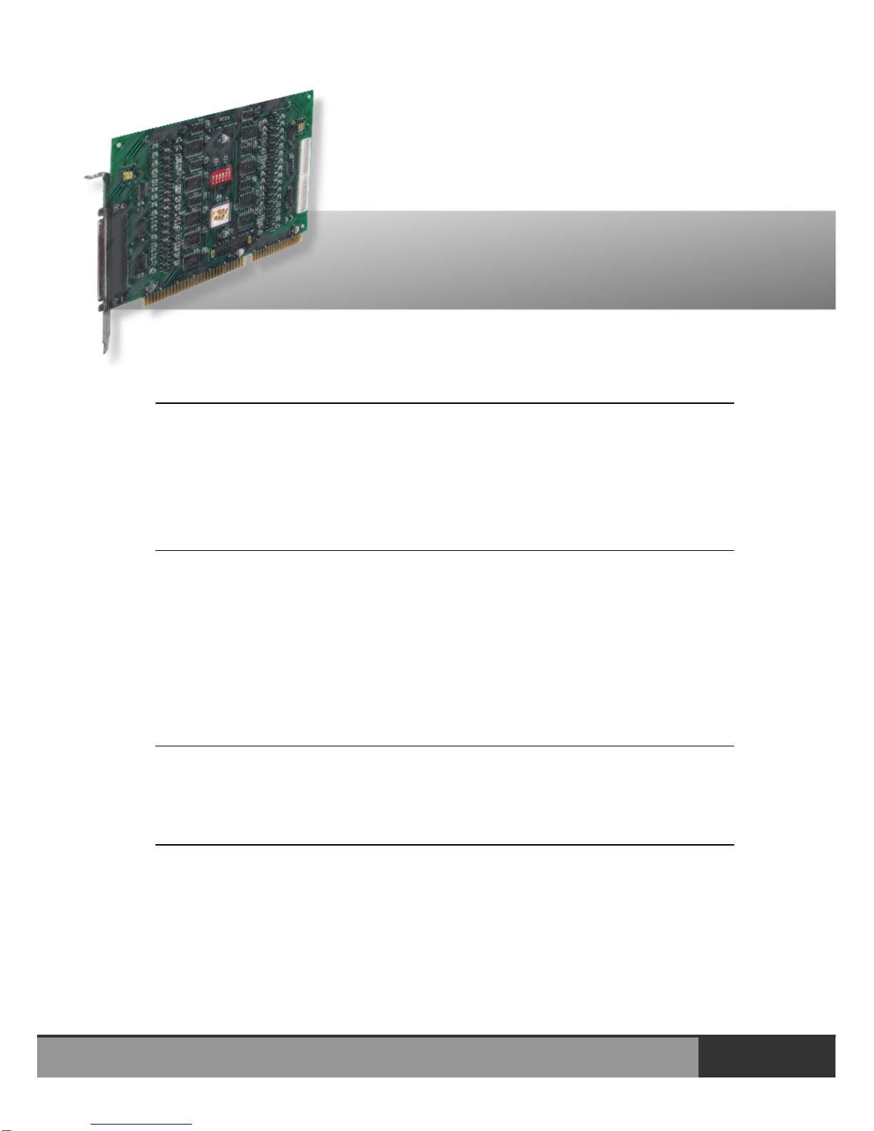
ISO-P32C32/P32S32W
ISO-P64/C64
User Manual
Version 1.9
Oct. 2011
Warranty
All products manufactured by ICP DAS are warranted against defective
materials for a period of one year from the date of delivery to the original
purchaser.
Warning
ICP DAS assumes no liability for damages consequent to the use of this product.
ICP DAS reserves the right to change this manual at any time without notice.
The information furnished by ICP DAS is believed to be accurate and reliable.
However, no responsibility is assumed by ICP DAS for its use, nor for any
infringements of patents or other rights of third parties resulting from its use.
Copyright
Copyright © 2011 by ICP DAS. All rights are reserved.
Trademark
Names are used for identification only and may be registered trademarks of their
respective companies.
ISO-P32C32/P32S32W/P64/C64 User Manual (Ver.1.9, Oct. 2011, IMH-000-19) 1

Tables of Contents
1. INTRODUCTION.........................................................................................................................4
1.1 SPECIFICATIONS ......................................................................................................................4
1.1.1 ISO-P32C32..........................................................................................................................4
1.1.2 ISO-P32S32W.......................................................................................................................5
1.1.3 ISO-P64 ................................................................................................................................6
1.1.4 ISO-C64................................................................................................................................6
1.2 ORDER DESCRIPTION...............................................................................................................7
1.3 OPTIONS..................................................................................................................................7
1.4 PRODUCT CHECK LIST.............................................................................................................8
2. HARDWARE CONFIGURATION..................................................................................................9
2.1 ISO-P32C32 BOARD LAYOUT.................................................................................................9
2.2 ISO-P32S32W BOARD LAYOUT ...........................................................................................10
2.2.1 Jumper Setting ....................................................................................................................11
2.2.2 IRQ Circuit diagram...........................................................................................................12
2.2.3 I/O Base Address Setting ....................................................................................................13
2.2.4 I/O Register Address...........................................................................................................16
2.3 ISO-P64 BOARD LAYOUT .....................................................................................................17
2.3.1 Jumper setting.....................................................................................................................18
2.3.2 I/O Base Address Setting ....................................................................................................18
2.3.3 I/O Register Address...........................................................................................................21
2.4 ISO-C64 BOARD LAYOUT.....................................................................................................22
2.4.1 I/O Base Address Setting ....................................................................................................23
2.4.2 I/O Register Address...........................................................................................................26
2.5 ISOLATED D/I ARCHITECTURE...............................................................................................27
2.5.1 Sample D/I Architecture for Internal Power ...................................................................29
2.5.2 Sample D/I Architecture for External Power...................................................................30
2.6 ISOLATED D/O ARCHITECTURE.............................................................................................31
2.6.1 Sample D/O Architecture.................................................................................................33
2.7 DAUGHTER BOARDS..............................................................................................................35
2.7.1 DB-37..................................................................................................................................35
2.7.2 DN-37..................................................................................................................................35
2.7.3 DB-8125 .......................................................................................................................... 35
2.8 PIN ASSIGNMENT OF ISO-P32C32 ........................................................................................36
2.9 PIN ASSIGNMENT OF ISO-P32S32W.....................................................................................37
2.10 PIN ASSIGNMENT OF ISO-P64...............................................................................................38
ISO-P32C32/P32S32W/P64/C64 User Manual (Ver.1.9, Oct. 2011, IMH-000-19) 2

ISO-P32C32/P32S32W/P64/C64 User Manual (Ver.1.9, Oct. 2011, IMH-000-19) 3
2.11 PIN ASSIGNMENT OF ISO-C64 ..............................................................................................39
3. THE APPLICATIONS OF DIGITAL I/O ................................................................................40
3.1 THE EXAMPLE OF ISO-P32C32............................................................................................. 40
3.2 THE EXAMPLE OF ISO-P64....................................................................................................43
3.3 THE EXAMPLE OF ISO-C64 ...................................................................................................46
4. DEMO PROGRAM.....................................................................................................................49
4.1 DEMO1 D/O FOR ISO-P32C32/P32S32W...........................................................................49
4.2 DEMO2 D/I FOR ISO-P32C32/P32S32W ............................................................................50
4.3 DEMO3 D/I/O FOR ISO-P32C32/P32S32W ........................................................................51
4.4 P32CINT.EXE INTERRUPT INPUT FOR ISO-P32C32/P32S32W..............................................53
4.5 DEMO1 D/I FOR ISO-P64 ....................................................................................................55
4.6 DEMO1 D/O FOR ISO-C64 ..................................................................................................56
1. Introduction
The ISO-P32C32/P32S32W consists of 32-channel isolated D/I and 32-
channels isolated D/O. The ISO-P64 consists of 64-channel isolated D/I. The
ISO-C64 consists of 64-channel isolated D/O. The D/I specifications of ISO-
P32C32/P32S32W & ISO-P64 are the same. The D/O specifications of ISO-
P32C32/P32S32W & ISO-C64 are the same.
1.1 Specifications
1.1.1 ISO-P32C32
Model Name ISO-P32C32
Digital Input
Isolation Voltage
3750 Vrms (Using external power)
3000 Vrms (Using internal power)
Channels 32
Compatibility Photo isolated current
Input Voltage
Logic 0: DC 0 ~ 1 V
Logic 1: DC 9 ~ 24 V
Input Impedance
3 KΩ, 0.5 W
Response Speed 4 kHz (Typical)
Digital Output
Isolation Voltage 3750 Vrms (Using external power)
Channels 32
Compatibility Sink, Open Collector
External Voltage 5 ~ 30 VDC (max.)
Output Capability
100 mA for one channel @ 100% duty
100 mA for all channels @ 100% duty
Response Speed 4 kHz (Typical)
General
Bus Type ISA
Data Bus 8-bit
I/O Connector Female DB37 x 1 ; 40-pin box header x 1
Dimensions (L x W x D) 163 mm x 115 mm x 22 mm
Power Consumption 600 mA @ +5 V
Operating Temperature 0 ~ 60 °C
Storage Temperature -20 ~ 70 °C
Humidity 5 ~ 85% RH, non-condensing
ISO-P32C32/P32S32W/P64/C64 User Manual (Ver.1.9, Oct. 2011, IMH-000-19) 4
ISO-P32C32/P32S32W/P64/C64 User Manual (Ver.1.9, Oct. 2011, IMH-000-19) 5
1.1.2 ISO-P32S32W
Model Name ISO-P32S32W
Digital Input
Isolation Voltage 3750 Vrms (Using external power)
Channels 32
Compatibility Photo isolated current
Input Voltage
Logic 0: DC 0 ~ 1 V
Logic 1: DC 5 ~ 24 V
Input Impedance 3 KΩ, 0.5 W
Response Speed 4 kHz (Typical)
Digital Output
Isolation Voltage 3750 Vrms (Using external power)
Channels 32
Compatibility Sink, Open Collector
External Voltage 5 ~ 30 VDC (max.)
500 mA for one high driving channel @ 100% duty
500 mA for all high driving channels @ 100% duty
(The GND pins all must be connected with GND of
External Power)
Output Capability
100 mA for one low driving channel @ 100% duty
100 mA for all low driving channels @ 100% duty
(The GND pins all must be connected with GND of
External Power)
Response Speed 4 kHz (Typical)
General
Bus Type ISA
Data Bus 8-bit
I/O Connector
Female DB37 x 1
40-pin Box header x 1
Dimensions (L x W x D) 163 mm x 115 mm x 22 mm
Power Consumption 600 mA @ +5 V
Operating Temperature 0 ~ 60 °C
Storage Temperature -20 ~ 70 °C
Humidity 5 ~ 85% RH, non-condensing
1.1.3 ISO-P64
Model Name ISO-P64
Digital Input
Isolation Voltage 3750 Vrms (Using external power)
3000 Vrms (Using internal power)
Channels 64
Compatibility Photo Coupler Isolated
Input Voltage Logic 0: DC 0 ~ 1 V
Logic 1: DC 9 ~ 24 V
Response Speed 4 kHz (Typical)
General
Bus Type ISA
Data Bus 8-bit
I/O Connector Female DB37 x 1 ; 40-pin Box header x 1
Dimensions (L x W x D) 175 mm x 115 mm x 22 mm
Power Consumption 400 mA @ +5 V
Operating Temperature 0 ~ 60 °C
Storage Temperature -20 ~ 70 °C
Humidity 5 ~ 85% RH, non-condensing
1.1.4 ISO-C64
Model Name ISO-C64
Digital Output
Isolation Voltage 3750 Vrms (Using external power)
Channels 64
Compatibility Sink, Open Collector
External Voltage 5 ~ 30 VDC (max.)
Output Capability 100 mA for one low driving channel @ 100% duty
100 mA for all low driving channels @ 60% duty
Response Speed 4 kHz (Typical)
General
Bus Type ISA
Data Bus 8-bit
I/O Connector Female DB37 x 1 ; 40-pin Box header x 1
Dimensions (L x W x D) 178 mm x 115 mm x 22mm
Power Consumption 500 mA @ +5 V
Operating Temperature 0 ~ 60 °C
Storage Temperature -20 ~ 70 °C
Humidity 5 ~ 85% RH, non-condensing
ISO-P32C32/P32S32W/P64/C64 User Manual (Ver.1.9, Oct. 2011, IMH-000-19) 6
ISO-P32C32/P32S32W/P64/C64 User Manual (Ver.1.9, Oct. 2011, IMH-000-19) 7
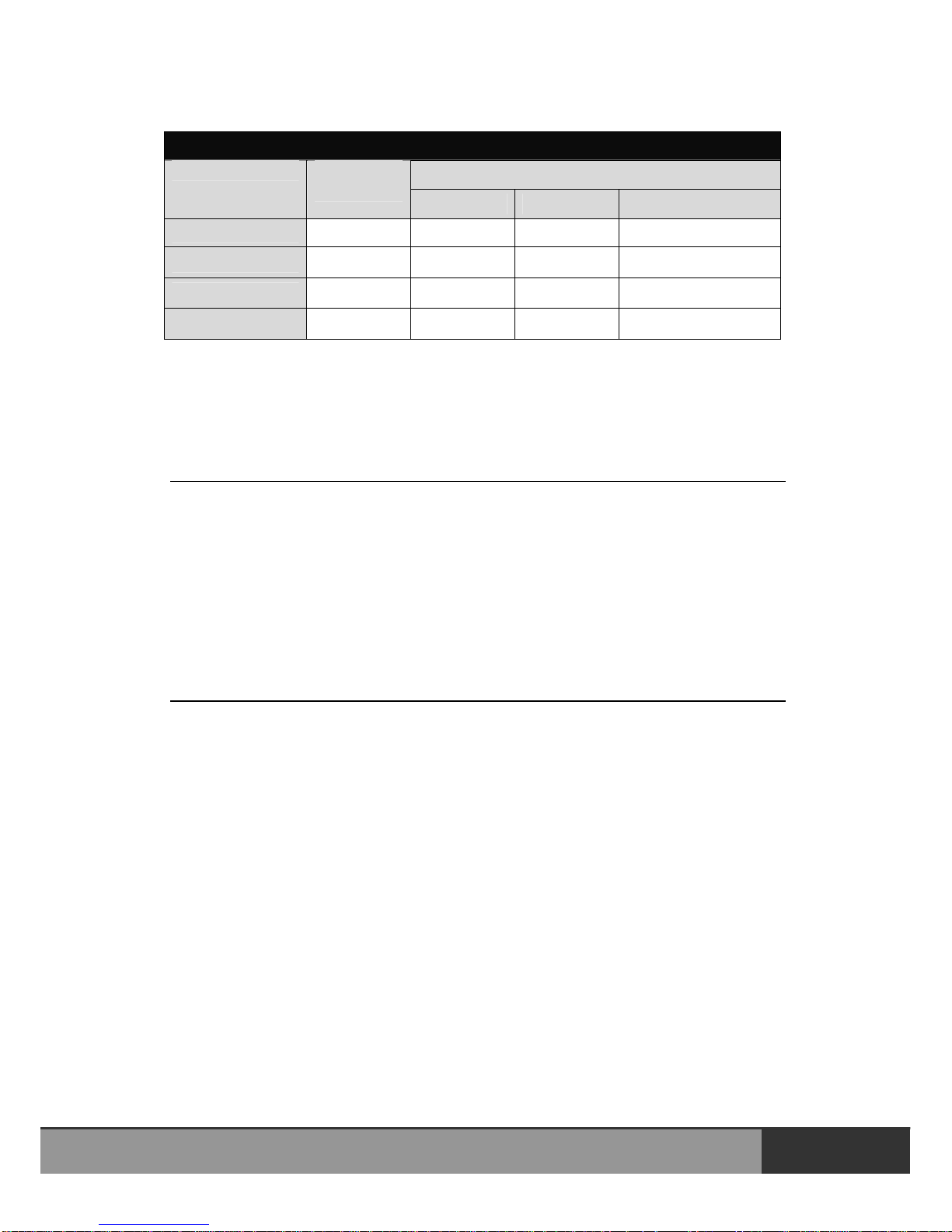
I/O channels
D/O channels
D/I
channels
Low Drive High Drive Type
ISO-P32S32W
32 24 8 Current Sink, NPN
ISO-P32C32
32 32 - Current Sink, NPN
ISO-P64
64 - - -
ISO-C64
- 64 - Current Sink, NPN
1.2 Order Description
ISO-P32C32/P32S32W: ISA bus D/I of 32-bit, D/O of 32-bit.
ISO-P64: ISA bus D/I of 64-bit.
ISO-C64: ISA bus D/O of 64-bit.
1.3 Options
ADP-37/PCI: extender, 50-pin OPTO-22 header to DB-37 for PCI Bus I/O
boards
ADP-50/PCI: extender, 50-pin OPTO-22 header to 50-pin header, for PCI
Bus I/O boards
DB32R: 32-channel relay output board (RoHS) Include : CA-3710D Male-
Male D-sub Cable 1.0 M
DB16P16R: 16-channel input terminal and 16-channel relay output board
Include : CA-3710D Male- Male D-sub Cable 1.0 M

1.4 Product Check List
The shipping package includes the following items:
One ISO-P32C32, ISO-P32S32W, ISO-P64 or ISO-C64 card
One software utility ISA CD.
One Quick Start Guide
It is recommended that you read the Quick Start Guide first. All the
necessary and essential information is given in the Quick Start Guide, including:
Where to get the software driver, demo programs and other resources.
How to install the software.
How to test the card.
Attention!
If any of these items is missing or damaged, contact the dealer from whom
you purchased the product. Please save the shipping materials and carton
in case you need to ship or store the product in the future.
ISO-P32C32/P32S32W/P64/C64 User Manual (Ver.1.9, Oct. 2011, IMH-000-19) 8
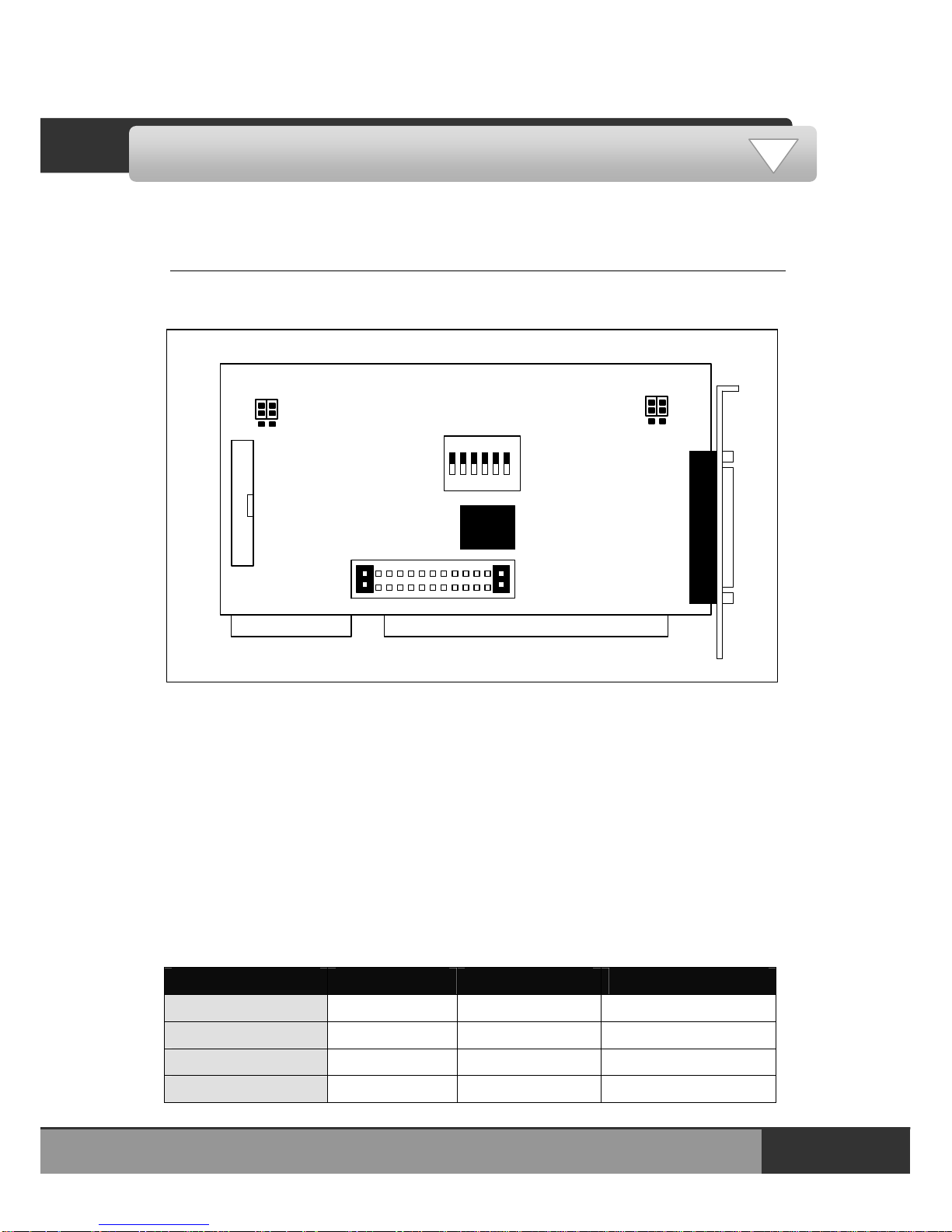
2. Hardware configuration 2. Hardware configuration
2.1 ISO-P32C32 Board Layout 2.1 ISO-P32C32 Board Layout
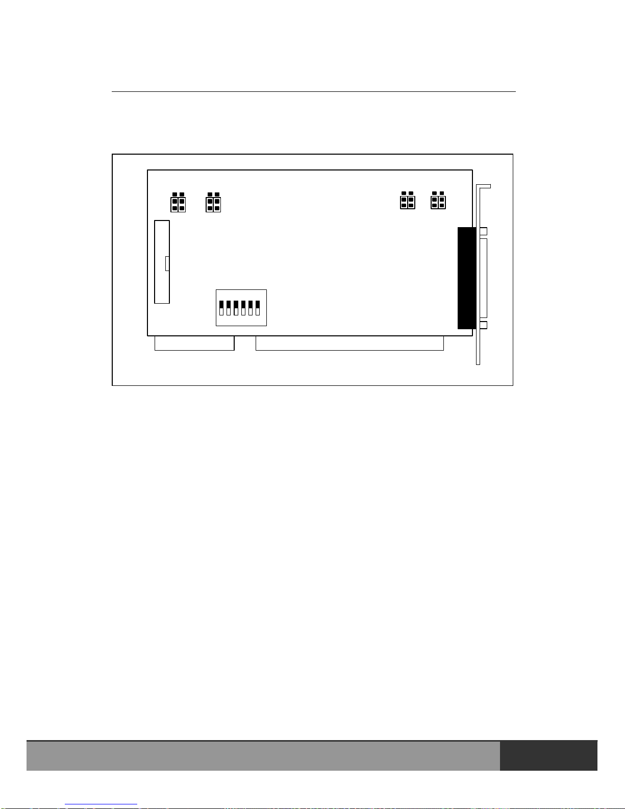
The board layout of ISO-P32C32 is given as follows:
JP3
ISA BUS
IRQ
ON
1 2 3 4 5 6
JP1
12
65
Internal
External
External
Internal
1
JP2
2
56
ISA BUS
ISO-P32C32
SW1
CON1
CON2
Figure 2-1: Board layout of ISO-P32C32
CON1: 40-PIN connector for D/I/O channel 16~31
CON2: 37-PIN D-sub connector for D/I/O channel 0~15
JP1: CON1 select internal/external power
JP2: CON2 select internal/external power
JP3: Interrupt levels selection (ISO-P32C32 provides IRQ9, 10,11,12,14
and 15)
SW1: I/O Address selection
DI/O Channel
DO Channel Power Ground
Isolation Bank 1
DI_0~15 (CON1, Pin18) (CON1, Pin19)
Isolation Bank 2
DO_0~15 (CON1, Pin37) (CON1, Pin1 & 20)
Isolation Bank 3
DI_16~31 (CON2, Pin18) (CON2, Pin19)
Isolation Bank 4
DO_16~31 (CON2, Pin37) (CON2, Pin1 & 20)
ISO-P32C32/P32S32W/P64/C64 User Manual (Ver.1.9, Oct. 2011, IMH-000-19) 9
ISO-P32C32/P32S32W/P64/C64 User Manual (Ver.1.9, Oct. 2011, IMH-000-19) 10
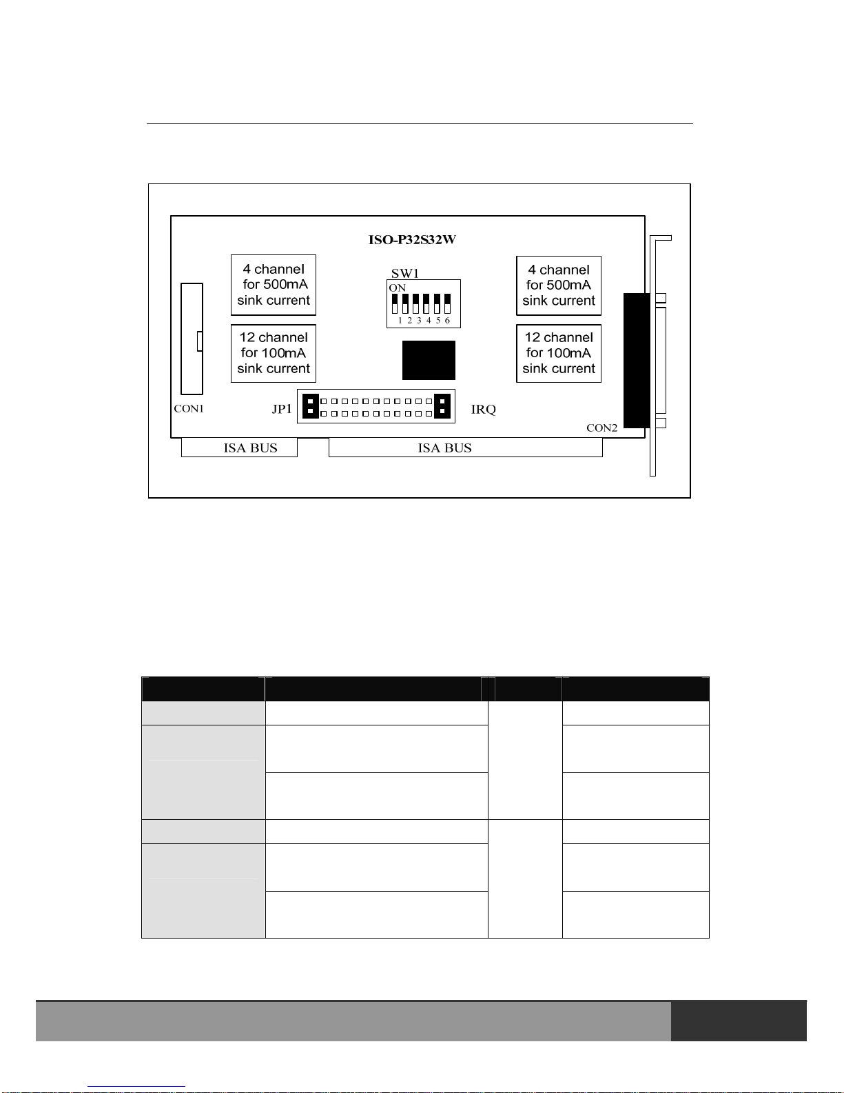
2.2 ISO-P32S32W Board Layout
The board layout of ISO-P32S32W is given as follow:
Figure 2-4. Board layout of ISO-P32S32W
CON1: 40-PIN connector for D/I/O channel 16~31
CON2: 37-PIN D-sub connector for D/I/O channel 0~15
JP1: Interrupt levels selection (ISO-P32S32W provides IRQ9,10,11,12,14
and 15)
SW1: I/O Address selection
DI/O Channel
DI/DO Channel Power Ground
Isolation Bank 1
DI_0~15 (CON1,Pin1)
DO_0~3 (High drive for 500 mA
sink current, NPN )
(CON1,Pin18 & Pin19)
Isolation Bank 2
DO_4~15(Low drive for 100 mA
sink current, NPN )
(CON1,Pi
n37)
(CON1,Pin1 & Pin20)
Isolation Bank 3
DI_16 ~ DI_31 (CON2,Pin1)
DO_16~19(High drive for 500 mA
sink current, NPN )
(CON2,Pin18 & Pin19)
Isolation Bank 4
DO_20~31(Low drive for 100 mA
sink current, NPN )
(CON2,Pi
n37)
(CON2,Pin1 & Pin20)
Attention: To prevent the board damaged forever by overload, the GND pins
(CON1: pin 1/ 18/ 19/ 20, CON2: pin 1/ 18/ 19/ 20) all must be connected with
GND of External Power.

2.2.1 Jumper Setting
JP1/JP2 Jumper setting (for ISO-P32C32):
External
Power
Internal
Power
Default Setting
JP1: CON1 Internal power/External selection.
JP2: CON2 Internal power/External selection.
IRQ selection : JP3 for ISO-P32C32
JP1 for ISO-P32S32W
N.C 15 14 12 11 10 9 7 6 5 4 3 N.C
Default IRQ: N.C (Not use IRQ)
Select IRQ one of the 3/4/5/6/7 for D/I channel 16 of CON1.
Select IRQ one of the 9/10/11/12/14/15 for D/I channel 0 of CON2.
Usage:
Step 1: Select IRQ 3/4/5/6/7 for channel 16.
Step 2: Select IRQ 9/10/11/12/14/15 for channel 0.
Step 3: Input interrupt signals by way of channel 0/16 of CON2/CON1.
Step 4: Run P32Cint.EXE used interrupt function for ISO-P32C32/
P32S32W card.
Step 5: Select I/O Base address of ISO-P32C32/P32S32W card.
Step 6: Input IRQ number (Refer to JP3 setting of P32C32 board,
JP1 setting of P32S32W board).
ISO-P32C32/P32S32W/P64/C64 User Manual (Ver.1.9, Oct. 2011, IMH-000-19) 11
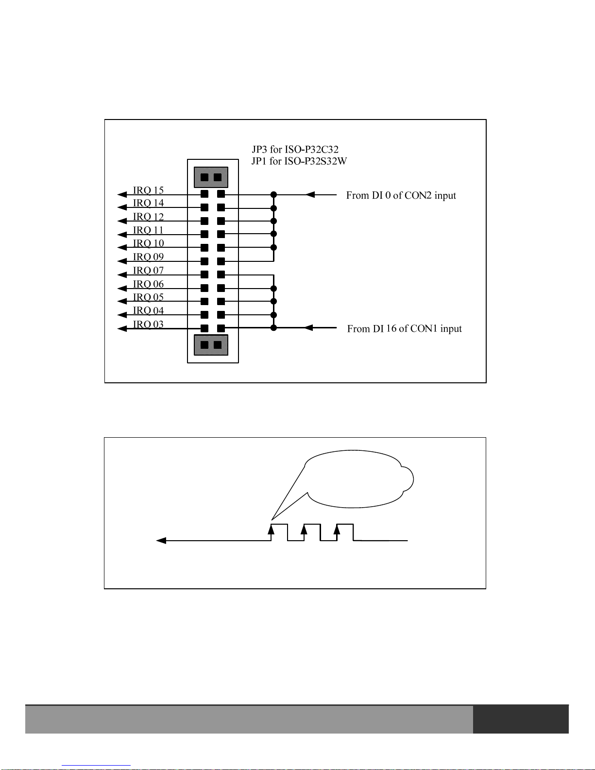
2.2.2 IRQ Circuit diagram
Figure 2-2: Select circuit diagram of IRQ for ISO-P32C32/P32S32W board.
External signal inupt to channel 0 or channel 16
Interrupt happend
to rising edge
Figure 2-3: Interrupt happened to rising edge.
ISO-P32C32/P32S32W/P64/C64 User Manual (Ver.1.9, Oct. 2011, IMH-000-19) 12
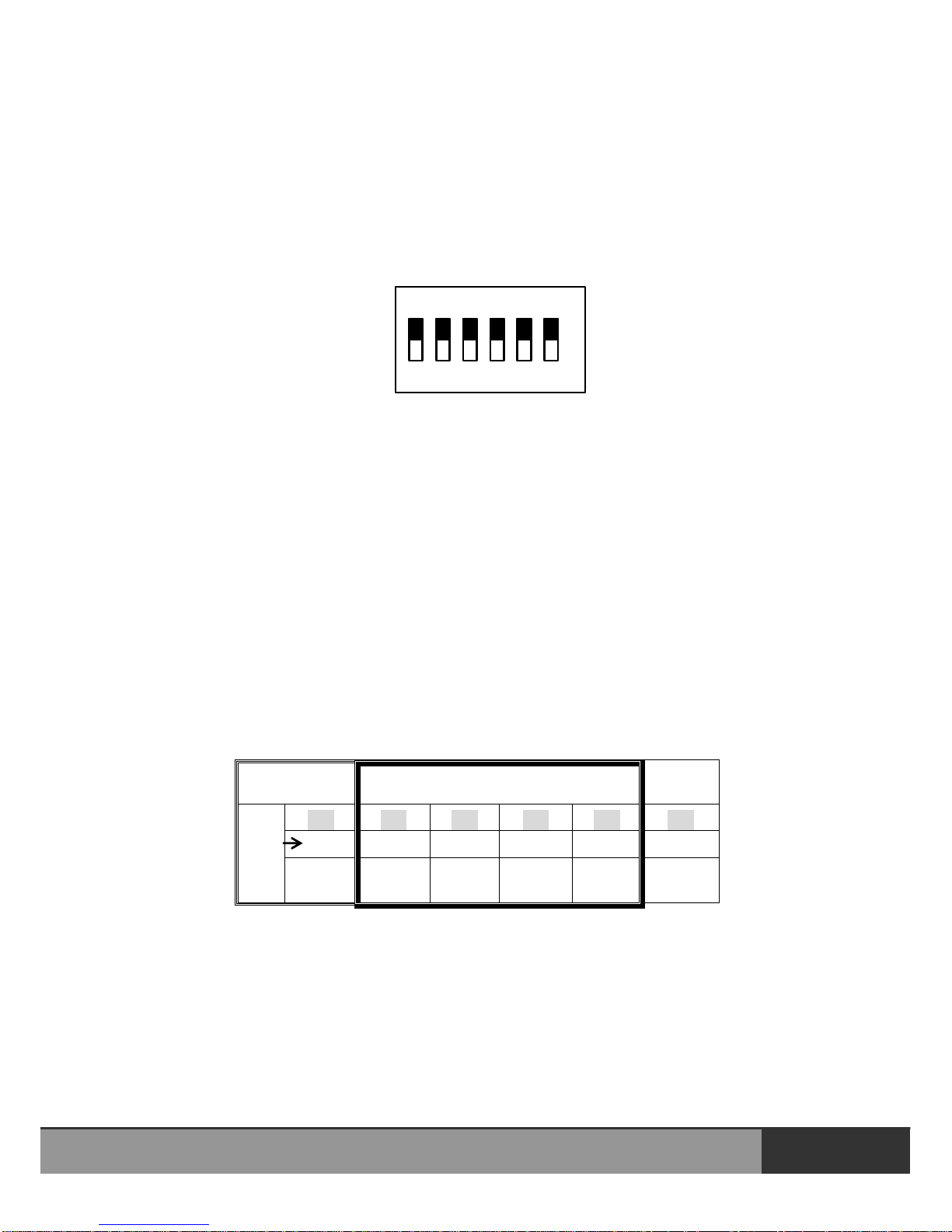
2.2.3 I/O Base Address Setting
The ISO-P32C32/P32S32W occupies 8 consecutive in I/O address space. The
base address is set by DIP switch SW1.
BASE ADDRESS
ON
1 2 3 4 5 6
SW1
Default Base Address 200 Hex
For Example
How to select 2 0 0 (Hex)
OFF Æ 1
ON Æ 0
2 0 0
ON ON ON ON ON ON
0 0 0 0 0 0
1
1
A8
2
A7
3
A6
4
A5
5
A4
6
A3
The detail SW1 base addresses setting. Please refer to ISOP32C32/P32S32W Base Address Table.
ISO-P32C32/P32S32W/P64/C64 User Manual (Ver.1.9, Oct. 2011, IMH-000-19) 13
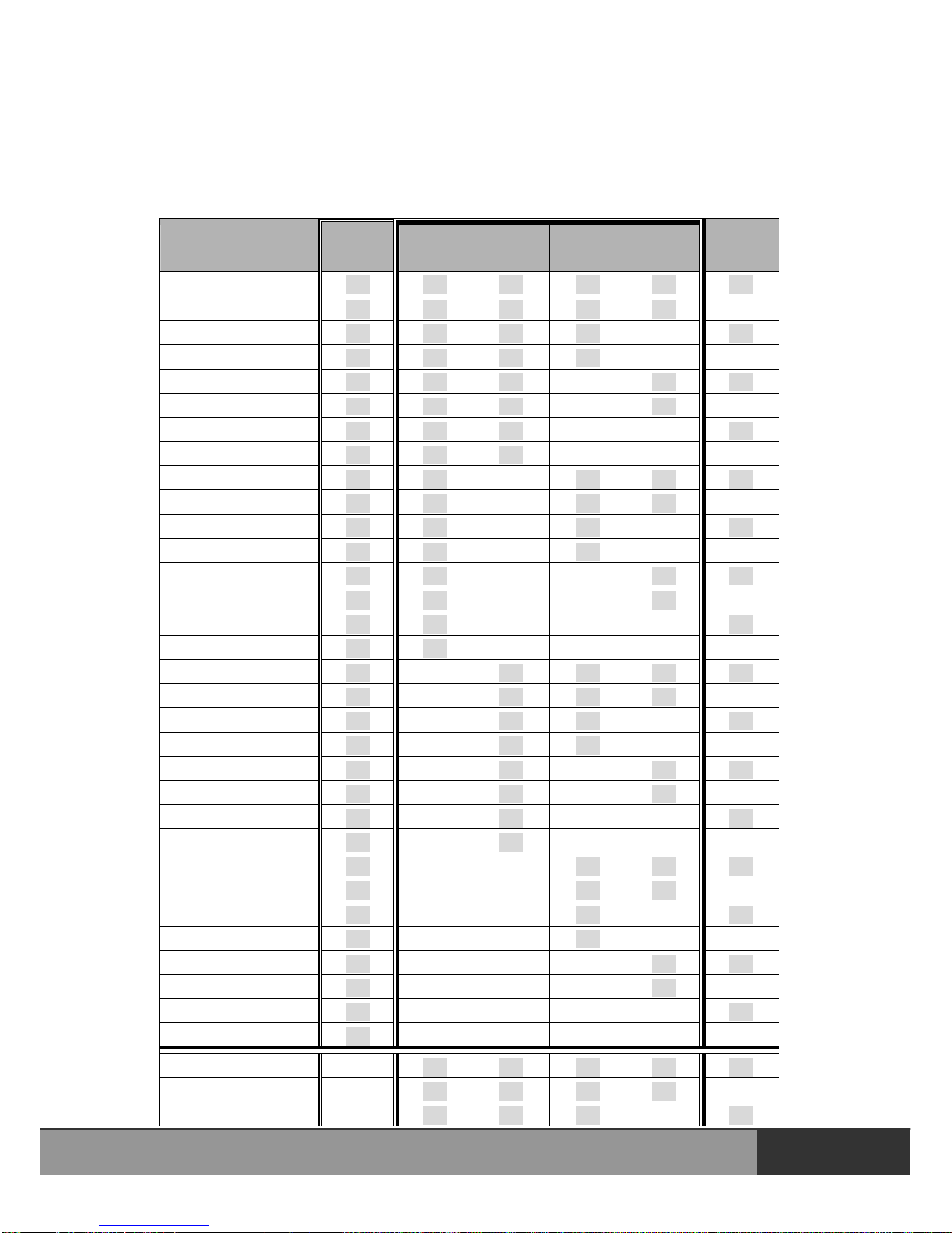
ISO-P32C32/P32S32W Base Address Table:
(*): Default setting
S1 Dip Switch
Address (Hex)
1
A8
2
A7
3
A6
4
A5
5
A4
6
A3
200 (*) ON ON ON ON ON ON
208 ON ON ON ON ON OFF
210 ON ON ON ON OFF ON
218 ON ON ON ON OFF OFF
220 ON ON ON OFF ON ON
228 ON ON ON OFF ON OFF
230 ON ON ON OFF OFF ON
238 ON ON ON OFF OFF OFF
240 ON ON OFF ON ON ON
248 ON ON OFF ON ON OFF
250 ON ON OFF ON OFF ON
258 ON ON OFF ON OFF OFF
260 ON ON OFF OFF ON ON
268 ON ON OFF OFF ON OFF
270 ON ON OFF OFF OFF ON
278 ON ON OFF OFF OFF OFF
280 ON OFF ON ON ON ON
288 ON OFF ON ON ON OFF
290 ON OFF ON ON OFF ON
298 ON OFF ON ON OFF OFF
2A0 ON OFF ON OFF ON ON
2A8 ON OFF ON OFF ON OFF
2B0 ON OFF ON OFF OFF ON
2B8 ON OFF ON OFF OFF OFF
2C0 ON OFF OFF ON ON ON
2C8 ON OFF OFF ON ON OFF
2D0 ON OFF OFF ON OFF ON
2D8 ON OFF OFF ON OFF OFF
2E0 ON OFF OFF OFF ON ON
2E8 ON OFF OFF OFF ON OFF
2F0 ON OFF OFF OFF OFF ON
2F8 ON OFF OFF OFF OFF OFF
300 OFF ON ON ON ON ON
308 OFF ON ON ON ON OFF
310 OFF ON ON ON OFF ON
ISO-P32C32/P32S32W/P64/C64 User Manual (Ver.1.9, Oct. 2011, IMH-000-19) 14
ISO-P32C32/P32S32W/P64/C64 User Manual (Ver.1.9, Oct. 2011, IMH-000-19) 15
318 OFF ON ON ON OFF OFF
320 OFF ON ON OFF ON ON
328 OFF ON ON OFF ON OFF
330 OFF ON ON OFF OFF ON
338 OFF ON ON OFF OFF OFF
340 OFF ON OFF ON ON ON
348 OFF ON OFF ON ON OFF
350 OFF ON OFF ON OFF ON
358 OFF ON OFF ON OFF OFF
360 OFF ON OFF OFF ON ON
368 OFF ON OFF OFF ON OFF
370 OFF ON OFF OFF OFF ON
378 OFF ON OFF OFF OFF OFF
380 OFF OFF ON ON ON ON
388 OFF OFF ON ON ON OFF
390 OFF OFF ON ON OFF ON
398 OFF OFF ON ON OFF OFF
3A0 OFF OFF ON OFF ON ON
3A8 OFF OFF ON OFF ON OFF
3B0 OFF OFF ON OFF OFF ON
3B8 OFF OFF ON OFF OFF OFF
3C0 OFF OFF OFF ON ON ON
3C8 OFF OFF OFF ON ON OFF
3D0 OFF OFF OFF ON OFF ON
3D8 OFF OFF OFF ON OFF OFF
3E0 OFF OFF OFF OFF ON ON
3E8 OFF OFF OFF OFF ON OFF
3F0 OFF OFF OFF OFF OFF ON
3F8 OFF OFF OFF OFF OFF OFF
2.2.4 I/O Register Address
The ISO-P32C32/P32S32W card occupies 8 consecutive PC I/O addresses.
The following table lists the registers and their locations.
D/I: digital input data format.
D/O: digital output data format.
ISO-P32C32/P32S32W I/O Register Address
Address Read Write ISO-P32C32/P32S32W
Base+0 D/I Channel 0~7 D/O Channel 0~7 CON 2
Base+1 D/I Channel 8~15 D/O Channel 8~15 CON 2
Base+2 D/I Channel 16~23 D/O Channel 16~23 CON 1
Base+3 D/I Channel 14~31 D/O Channel 14~31 CON 1
Read/Write Base+0
Bit 7 6 5 4 3 2 1 0
Channel
7 6 5 4 3 2 1 0
Read/Write Base+1
Bit 7 6 5 4 3 2 1 0
Channel
15 14 13 12 11 10 9 8
Read/Write Base+2
Bit 7 6 5 4 3 2 1 0
Channel
23 22 21 20 19 18 17 16
Read/Write Base+3
Bit 7 6 5 4 3 2 1 0
Channel
31 30 29 28 27 26 25 24
ISO-P32C32/P32S32W/P64/C64 User Manual (Ver.1.9, Oct. 2011, IMH-000-19) 16
2.3 ISO-P64 Board Layout
The board layout of ISO-P64 is given as follows:
ISA BUS
ON
1 2 3 4 5 6
JP4
Internal
External External
Internal
JP2
ISA BUS
ISO-P64
126512
65
126512
65
JP3
JP2JP1
CON1
CON2
SW1
Figure 2-5: Board layout of ISO-P64
JP1: select internal/external power for DI_0 ~ DI_15 (3000 V isolation)
JP2: select internal/external power for DI_16 ~ DI_31 (3000 V isolation)
JP3: select internal/external power for DI_47 ~ DI_32 (3000 V isolation)
JP4: select internal/external power for DI_63 ~ DI_48 (3000 V isolation)
Isolation bank 1: DI_0 ~ DI_15, Power=CON1_18, Ground=CON1_1
Isolation bank 2: DI_16 ~ DI_31, Power=CON1_37, Ground=CON1_20
Isolation bank 3: DI_32 ~ DI_47, Power=CON2_18, Ground=CON2_1
Isolation bank 4: DI_48 ~ DI_63, Power=CON2_37, Ground=CON2_20
All these four banks are fully isolated from each other.
The DC/DC1 is used to provide the internal power supply for bank1 & bank2.
The DC/DC2 is used to provide the internal power supply for bank3 & bank4.
ISO-P32C32/P32S32W/P64/C64 User Manual (Ver.1.9, Oct. 2011, IMH-000-19) 17

2.3.1 Jumper setting
JP1/JP2/JP3/JP4 jumper setting:
Internal
Power
External
Power
Default Setting
2.3.2 I/O Base Address Setting
ON
1 2 3 4 5 6
BASE ADDRESS
SW1
Default Base Address 200 Hex
For Example: How to select 2 0 0 (Hex)
OFF Æ 1
ON Æ 0
2 0 0
ON ON ON ON ON ON
0 0 0 0 0 0
1
1
A8
2
A7
3
A6
4
A5
5
A4
6
A3
The detail SW1 base addresses setting. Please refer to ISO-P64
Base Address Table.
ISO-P32C32/P32S32W/P64/C64 User Manual (Ver.1.9, Oct. 2011, IMH-000-19) 18

ISO-P64 Base Address Table:
(*): Default setting
S1 Dip Switch
Address (Hex)
1
A8
2
A7
3
A6
4
A5
5
A4
6
A3
200 (*) ON ON ON ON ON ON
208 ON ON ON ON ON OFF
210 ON ON ON ON OFF ON
218 ON ON ON ON OFF OFF
220 ON ON ON OFF ON ON
228 ON ON ON OFF ON OFF
230 ON ON ON OFF OFF ON
238 ON ON ON OFF OFF OFF
240 ON ON OFF ON ON ON
248 ON ON OFF ON ON OFF
250 ON ON OFF ON OFF ON
258 ON ON OFF ON OFF OFF
260 ON ON OFF OFF ON ON
268 ON ON OFF OFF ON OFF
270 ON ON OFF OFF OFF ON
278 ON ON OFF OFF OFF OFF
280 ON OFF ON ON ON ON
288 ON OFF ON ON ON OFF
290 ON OFF ON ON OFF ON
298 ON OFF ON ON OFF OFF
2A0 ON OFF ON OFF ON ON
2A8 ON OFF ON OFF ON OFF
2B0 ON OFF ON OFF OFF ON
2B8 ON OFF ON OFF OFF OFF
2C0 ON OFF OFF ON ON ON
2C8 ON OFF OFF ON ON OFF
2D0 ON OFF OFF ON OFF ON
2D8 ON OFF OFF ON OFF OFF
2E0 ON OFF OFF OFF ON ON
2E8 ON OFF OFF OFF ON OFF
2F0 ON OFF OFF OFF OFF ON
2F8 ON OFF OFF OFF OFF OFF
300 OFF ON ON ON ON ON
308 OFF ON ON ON ON OFF
310 OFF ON ON ON OFF ON
318 OFF ON ON ON OFF OFF
ISO-P32C32/P32S32W/P64/C64 User Manual (Ver.1.9, Oct. 2011, IMH-000-19) 19

ISO-P32C32/P32S32W/P64/C64 User Manual (Ver.1.9, Oct. 2011, IMH-000-19) 20
320 OFF ON ON OFF ON ON
328 OFF ON ON OFF ON OFF
330 OFF ON ON OFF OFF ON
338 OFF ON ON OFF OFF OFF
340 OFF ON OFF ON ON ON
348 OFF ON OFF ON ON OFF
350 OFF ON OFF ON OFF ON
358 OFF ON OFF ON OFF OFF
360 OFF ON OFF OFF ON ON
368 OFF ON OFF OFF ON OFF
370 OFF ON OFF OFF OFF ON
378 OFF ON OFF OFF OFF OFF
380 OFF OFF ON ON ON ON
388 OFF OFF ON ON ON OFF
390 OFF OFF ON ON OFF ON
398 OFF OFF ON ON OFF OFF
3A0 OFF OFF ON OFF ON ON
3A8 OFF OFF ON OFF ON OFF
3B0 OFF OFF ON OFF OFF ON
3B8 OFF OFF ON OFF OFF OFF
3C0 OFF OFF OFF ON ON ON
3C8 OFF OFF OFF ON ON OFF
3D0 OFF OFF OFF ON OFF ON
3D8 OFF OFF OFF ON OFF OFF
3E0 OFF OFF OFF OFF ON ON
3E8 OFF OFF OFF OFF ON OFF
3F0 OFF OFF OFF OFF OFF ON
3F8 OFF OFF OFF OFF OFF OFF

2.3.3 I/O Register Address
The ISO-P64 card occupies 8 consecutive PC I/O address. The following table
lists the registers and their locations.
ISO-P64 I/O Register Address
Address D/I Channel ISO-P64
Base+0
Channel 0~7 Read Only
Base+1
Channel 8~15 Read Only
Base+2
Channel 16~23 Read Only
Base+3
Channel 24~31 Read Only
Base+4
Channel 32~39 Read Only
Base+5
Channel 40~47 Read Only
Base+6
Channel 48~55 Read Only
Base+7
Channel 56~63 Read Only
Read
Bit D7 D6 D5 D4 D3 D2 D1 D0
Base+0
7 6 5 4 3 2 1 0
Base+1
15 14 13 12 11 10 9 8
Base+2
23 22 21 20 19 18 17 16
Base+3
31 30 29 28 27 26 25 24
Base+4
39 38 37 36 35 34 33 32
Base+5
47 46 45 44 43 42 41 40
Base+6
55 54 53 52 51 50 49 48
Base+7
63 62 61 60 59 58 57 56
ISO-P32C32/P32S32W/P64/C64 User Manual (Ver.1.9, Oct. 2011, IMH-000-19) 21

2.4 ISO-C64 Board Layout
The board layout of ISO-C64 is given as follows:
SW1
ISA BUS
ON
1 2 3 4 5 6
ISA BUS
ISO-C64
LED1LED2LED3LED4
CON1
CON2
Figure 2-6: Board layout of ISO-C64
LED 1: power indicator for DO_0 ~ DO_15
LED 2: power indicator for DO_31 ~ DO_16
LED 3: power indicator for DO_47 ~ DO_32
LED 4: power indicator for DO_63 ~ DO_48
Isolation bank 1: DO_0 ~ DO_15, Power=CON1_18, Ground=CON1_1
Isolation bank 2: DO_16 ~ DO_31, Power=CON1_37, Ground=CON1_20
Isolation bank 3: DO_32 ~ DO_47, Power=CON2_18, Ground=CON2_1
Isolation bank 4: DO_48 ~ DO_63, Power=CON2_37, Ground=CON2_20
All these four banks are fully isolated from each other.
ISO-P32C32/P32S32W/P64/C64 User Manual (Ver.1.9, Oct. 2011, IMH-000-19) 22

2.4.1 I/O Base Address Setting
BASE ADDRESS
ON
1 2 3 4 5 6
SW1
Default base Address 200 Hex
For Example
How to select 2 0 0 (Hex)
OFF Æ 1
ON Æ 0
2 0 0
ON ON ON ON ON ON
0 0 0 0 0 0
1
1
A8
2
A7
3
A6
4
A5
5
A4
6
A3
The detail SW1 base addresses setting. Please refer to ISO-C64 Base
Address Table.
ISO-P32C32/P32S32W/P64/C64 User Manual (Ver.1.9, Oct. 2011, IMH-000-19) 23

ISO-C64 Base Address Table:
(*): Default setting
S1 Dip Switch
Address (Hex)
1
A8
2
A7
3
A6
4
A5
5
A4
6
A3
200 (*) ON ON ON ON ON ON
208 ON ON ON ON ON OFF
210 ON ON ON ON OFF ON
218 ON ON ON ON OFF OFF
220 ON ON ON OFF ON ON
228 ON ON ON OFF ON OFF
230 ON ON ON OFF OFF ON
238 ON ON ON OFF OFF OFF
240 ON ON OFF ON ON ON
248 ON ON OFF ON ON OFF
250
ON ON OFF ON OFF ON
258 ON ON OFF ON OFF OFF
260 ON ON OFF OFF ON ON
268 ON ON OFF OFF ON OFF
270 ON ON OFF OFF OFF ON
278 ON ON OFF OFF OFF OFF
280 ON OFF ON ON ON ON
288 ON OFF ON ON ON OFF
290 ON OFF ON ON OFF ON
298 ON OFF ON ON OFF OFF
2A0 ON OFF ON OFF ON ON
2A8 ON OFF ON OFF ON OFF
2B0 ON OFF ON OFF OFF ON
2B8 ON OFF ON OFF OFF OFF
2C0 ON OFF OFF ON ON ON
2C8 ON OFF OFF ON ON OFF
2D0 ON OFF OFF ON OFF ON
2D8 ON OFF OFF ON OFF OFF
2E0 ON OFF OFF OFF ON ON
2E8 ON OFF OFF OFF ON OFF
2F0 ON OFF OFF OFF OFF ON
2F8 ON OFF OFF OFF OFF OFF
300 OFF ON ON ON ON ON
308 OFF ON ON ON ON OFF
310 OFF ON ON ON OFF ON
318 OFF ON ON ON OFF OFF
320 OFF ON ON OFF ON ON
ISO-P32C32/P32S32W/P64/C64 User Manual (Ver.1.9, Oct. 2011, IMH-000-19) 24

ISO-P32C32/P32S32W/P64/C64 User Manual (Ver.1.9, Oct. 2011, IMH-000-19) 25
328 OFF ON ON OFF ON OFF
330 OFF ON ON OFF OFF ON
338 OFF ON ON OFF OFF OFF
340 OFF ON OFF ON ON ON
348 OFF ON OFF ON ON OFF
350 OFF ON OFF ON OFF ON
358 OFF ON OFF ON OFF OFF
360 OFF ON OFF OFF ON ON
368 OFF ON OFF OFF ON OFF
370 OFF ON OFF OFF OFF ON
378 OFF ON OFF OFF OFF OFF
380 OFF OFF ON ON ON ON
388 OFF OFF ON ON ON OFF
390 OFF OFF ON ON OFF ON
398 OFF OFF ON ON OFF OFF
3A0 OFF OFF ON OFF ON ON
3A8 OFF OFF ON OFF ON OFF
3B0 OFF OFF ON OFF OFF ON
3B8 OFF OFF ON OFF OFF OFF
3C0 OFF OFF OFF ON ON ON
3C8 OFF OFF OFF ON ON OFF
3D0 OFF OFF OFF ON OFF ON
3D8 OFF OFF OFF ON OFF OFF
3E0 OFF OFF OFF OFF ON ON
3E8 OFF OFF OFF OFF ON OFF
3F0 OFF OFF OFF OFF OFF ON
3F8 OFF OFF OFF OFF OFF OFF

2.4.2 I/O Register Address
The ISO-C64 card occupies 8 consecutive PC I/O address. The following table
lists the registers and their locations.
ISO-C64 I/O Register Address
Address D/O Channel ISO-C64
Base+0
Channel 0~7 Write Only
Base+1
Channel 8~15 Write Only
Base+2
Channel 16~23 Write Only
Base+3
Channel 24~31 Write Only
Base+4
Channel 32~39 Write Only
Base+5
Channel 40~47 Write Only
Base+6
Channel 48~55 Write Only
Base+7
Channel 56~63 Write Only
Write
Bit D7 D6 D5 D4 D3 D2 D1 D0
Base+0
7 6 5 4 3 2 1 0
Base+1
15 14 13 12 11 10 9 8
Base+2
23 22 21 20 19 18 17 16
Base+3
31 30 29 28 27 26 25 24
Base+4
39 38 37 36 35 34 33 32
Base+5
47 46 45 44 43 42 41 40
Base+6
55 54 53 52 51 50 49 48
Base+7
63 62 61 60 59 58 57 56
ISO-P32C32/P32S32W/P64/C64 User Manual (Ver.1.9, Oct. 2011, IMH-000-19) 26

2.5 Isolated D/I Architecture
The D/I architecture of ISO-P32C32 & ISO-P64 are the same. The User can
select internal power or external power to supply photo-couple digital input
power. The ISO-P32S32W only used external Power. The block diagram of D/I
are given as follows:
Configure 1: Internal power supply (Default Setting)
Figure 2-6: Isolated D/I Architecture with internal power supply
R=3K
D in
Vcc
R=10k
External source signal
DC / DC
PC's
Power
In
Out
(-) External GND
(+) Internal
(-) GND Internal
(-) GND
(+)
ISO-P32C32 / P32S32W/ P64
Figure 2-7: Typical Applications of D/I with internal power supply.
ISO-P32C32/P32S32W/P64/C64 User Manual (Ver.1.9, Oct. 2011, IMH-000-19) 27

ISO-P32C32/P32S32W/P64/C64 User Manual (Ver.1.9, Oct. 2011, IMH-000-19) 28
Configure 2: External power supply
R=3K
D in
Vcc
R=10k
DC / DC
PC's
Power
In
Out
(+) Internal
(-) GND Internal
ISO-P32C32 / P32S32W / P64
D Input (External)
(+) External Power
(-) External GND
Figure 2-8: Isolated D/I Architecture with external power supply
Figure 2-9: Typical Applications of D/I with external power supply.

2.5.1 Sample D/I Architecture for Internal Power
R=3K
DI 0
Vcc
R=4.7k
D
DC / DC
PC's
Power
In
Out
(+) Internal
(-) GND Internal
ISO-P32C32 & ISO-P64
(-) External GND
R=3K
R=4.7k
D
R=3K
R=4.7k
D
DI 1
DI 2
Switch 0
Switch 2
Switch
31
Vcc
Vcc
ISO-P32C32/P32S32W/P64/C64 User Manual (Ver.1.9, Oct. 2011, IMH-000-19) 29

2.5.2 Sample D/I Architecture for External
Power
ISO-P32C32/P32S32W/P64/C64 User Manual (Ver.1.9, Oct. 2011, IMH-000-19) 30

2.6 Isolated D/O Architecture
The D/O architecture of ISO-P32C32/P32S32W & ISO-C64 are the same. The
block diagrams of D/O are given as follows:
Figure 2-10: Isolated D/O Architecture
Figure 2-11: Typical Applications of D/O
ISO-P32C32/P32S32W/P64/C64 User Manual (Ver.1.9, Oct. 2011, IMH-000-19) 31

ISO-P32C32/P32S32W/P64/C64 User Manual (Ver.1.9, Oct. 2011, IMH-000-19) 32
NOTE:
1. The ISO-P32C32/C64, I1, I2, … & I32 must be < 100 mA . The ISO-
P32S32W ,
I1~I4 & I17~I20 must be ≦500 mA , The other must be < 100 mA .
2. The R1, R2, ... & R32 are current-limit resistors. They must be designed to
let I1, I2, ... & I32 <100 mA for ISO-P32C32/C64. I1~4 & I17~20 ≦500 mA
for ISO-P32S32W.
3. If the internal resistance of external device is large enough, the R can be
omitted.
4. The D1, D2, ... & D31 are common-cathode diodes for switching inductive
lords. They can be used as relay driver, hammer driver, lamp driver, display
driver, line driver & logic buffers.

ISO-P32C32/P32S32W/P64/C64 User Manual (Ver.1.9, Oct. 2011, IMH-000-19) 33
2.6.1 Sample D/O Architecture

Open-Collector wiring Notice
ISO-P32C32/P32S32W/P64/C64 User Manual (Ver.1.9, Oct. 2011, IMH-000-19) 34

2.7 Daughter Boards
2.7.1 DB-37
The DB-37 is a general purpose daughter board for D-sub 37 pins. It is
designed for easy wire connection.
37-Pin Cable
37-Pin Cable
37-Pin Cable
DB-37
2.7.2 DN-37
The DN-37 is a general purpose daughter board for DB-37 with DIN-Rail
Mounting. It is designed for easy wire connection.
DN-37
2.7.3 DB-8125
The DB-8125 is a general purpose screw terminal board. It is designed for easy
wire connection. There are one DB-37 & two 20-pin flat-cable headers in the DB-
8125.
20-pin flat-cable header)
(for DB-37 or
DB-8125
ISO-P32C32/P32S32W/P64/C64 User Manual (Ver.1.9, Oct. 2011, IMH-000-19) 35

ISO-P32C32/P32S32W/P64/C64 User Manual (Ver.1.9, Oct. 2011, IMH-000-19) 36
2.8 Pin Assignment of ISO-P32C32
DI: 0-15 (-)
20
22
21
23
24
25
26
27
28
29
30
31
32
33
34
35
36
37
DO: 0-15 (+)
1
2
3
4
5
15
14
13
12
11
10
9
8
7
6
19
18
17
16
DI 10
DI 13
DI 12
DI 11
DI 14
DI 15
DI 0
DI 6
DI 5
DI 4
DI 3
DI 2
DI 1
DI 7
DI 8
DI 9
DI: 0-15 (+)
DO: 0-15 (-)
DO 0
DO 1
DO 2
DO 3
DO 4
DO 5
DO 6
DO 7
DO 8
DO 9
DO 10
DO 11
DO 12
DO 13
DO 14
DO 15
DO: 0-15 (-)
External
Power GND (-)
External
Power GND (-)
External
Power (+)
External
Power GND (-)
External
Power (+)
DI: 16-31 (-)
20
22
21
23
24
25
26
27
28
29
30
31
32
33
34
35
36
37
DO: 16-31 (+)
1
2
3
4
5
15
14
13
12
11
10
9
8
7
6
19
18
17
16
DI 26
DI 29
DI 28
DI 27
DI 30
DI 31
DI 16
DI 22
DI 21
DI 20
DI 19
DI 18
DI 17
DI 23
DI 24
DI 25
DI: 16-31 (+)
DO:16-31 (-)
DO 16
DO 17
DO 18
DO 19
DO 20
DO 21
DO 22
DO 23
DO 24
DO 25
DO 26
DO 27
DO 28
DO 29
DO 30
DO 31
DO: 16-31 (-)
External
Power GND (-)
External
Power GND (-)
External
Power (+)
External
Power GND (-)
External
Power (+)
2
6
4
8
10
12
14
16
18
20
22
24
26
28
30
32
34
36
1
19
29
27
25
23
21
37
35
33
31
3
5
7
9
17
15
13
11
39
40
38
DI 16
DI 22
DI 21
DI 20
DI 19
DI 18
DI 17
DI 23
DI 24
DI 25
DI 31
DI 30
DI 29
DI 28
DI 27
DI 26
DO 25
DO 31
DO 30
DO 29
DO 28
DO 27
DO 26
CON1 D/O External
Power (+)
DO 16
DO 22
DO 21
DO 20
DO 19
DO 18
DO 17
DO 23
DO 24
N.C.
N.C.
CON1 D/O External
Power GND (-)
CON1 D/O External
Power GND (-)
CON1 D/I Power (+)
CON1 D/I Power (-)
N.C.
CON2: Pin assignment
CON1: Pin assignment
DB-40-Pin conversion DB-37-Pin
CON1: Pin assignment
Pin assignment of CON1 via extension cable
JP3
ISA BUS
IRQ
ON
1 2 3 4 5 6
JP1
12
65
Internal
External
External
Internal
1
JP2
2
56
ISA BUS
CON2
ISO-P32C32
SW1
CON1
Extension Cable

ISO-P32C32/P32S32W/P64/C64 User Manual (Ver.1.9, Oct. 2011, IMH-000-19) 37
2.9 Pin Assignment of ISO-P32S32W
20
22
21
23
24
25
26
27
28
29
30
31
32
33
34
35
36
37
1
2
3
4
5
15
14
13
12
11
10
9
8
7
6
19
18
17
16
DI 10
DI 13
DI 12
DI 11
DI 14
DI 15
DI 0
DI 6
DI 5
DI 4
DI 3
DI 2
DI 1
DI 7
DI 8
DI 9
DO 0 for High drive
DO 1 for High drive
DO 2 for High drive
DO 3 for High drive
DO 4
DO 5
DO 6
DO 7
DO 8
DO 9
DO 10
DO 11
DO 12
DO 13
DO 14
DO 15
External
Power GND (-)
External
Power GND (-)
GND for High Drive
GND for High Drive
External
Power (+)
20
22
21
23
24
25
26
27
28
29
30
31
32
33
34
35
36
37
1
2
3
4
5
15
14
13
12
11
10
9
8
7
6
19
18
17
16
DI 26
DI 29
DI 28
DI 27
DI 30
DI 31
DI 16
DI 22
DI 21
DI 20
DI 19
DI 18
DI 17
DI 23
DI 24
DI 25
DO 20
DO 21
DO 22
DO 23
DO 24
DO 25
DO 26
DO 27
DO 28
DO 29
DO 30
DO 31
External
Power GND (-)
External
Power GND (-)
DO 16 for
High drive
DO 16 for High drive
DO 17 for High drive
DO 18 for High drive
DO 19 for High drive
GND for High Drive
GND for High Drive
2
6
4
8
10
12
14
16
18
20
22
24
26
28
30
32
34
36
1
19
29
27
25
23
21
37
35
33
31
3
5
7
9
17
15
13
11
39
40
38
DI 16
DI 22
DI 21
DI 20
DI 19
DI 18
DI 17
DI 23
DI 24
DI 25
DI 31
DI 30
DI 29
DI 28
DI 27
DI 26
DO 25
DO 31
DO 30
DO 29
DO 28
DO 27
DO 26
CON1 D/O External
Power (+)
DO 16 for High drive
DO 22
DO 21
DO 20
DO 19 for High drive
DO 18 for High drive
DO 17 for High drive
DO 23
DO 24
N.C.
N.C.
CON1 D/O External
Power GND (-)
CON1 D/O External
Power GND (-)
GND for High Drive
GND for High Drive
N.C.
CON2: Pin assignment
CON1: Pin assignment
DB-40-Pin conversion DB-37-Pin
CON1: Pin assignment
Pin assignment of CON1 via extension cable
ISA BUS
IRQ
ON
1 2 3 4 5 6
ISA BUS
SW1
CON1
CON2
ISO-P32S32W
JP1
Extension Cable

ISO-P32C32/P32S32W/P64/C64 User Manual (Ver.1.9, Oct. 2011, IMH-000-19) 38
2.10 Pin Assignment of ISO-P64
N.C.
20
22
21
23
24
25
26
27
28
29
30
31
32
33
34
35
36
37
DI: 16-31(+)
1
2
3
4
5
15
14
13
12
11
10
9
8
7
6
19
18
17
16
DI 10
DI 13
DI 12
DI 11
DI 14
DI 15
DI 0
DI 6
DI 5
DI 4
DI 3
DI 2
DI 1
DI 7
DI 8
DI 9
DI: 0-15 (+)
DI: 0-15 (-)
DI 16
DI 17
DI 18
DI 19
DI 20
DI 21
DI 22
DI 23
DI 24
DI 25
DI 26
DI 27
DI 28
DI 29
DI 30
DI 31
DI: 16-31 (-)
External
Power GND(-)
External
Power GND(-)
External
Power (+)
External
Power GND(-)
N.C.
20
22
21
23
24
25
26
27
28
29
30
31
32
33
34
35
36
37
DI: 48-63 (+)
1
2
3
4
5
15
14
13
12
11
10
9
8
7
6
19
18
17
16
DI 42
DI 45
DI 44
DI 43
DI 46
DI 47
DI 32
DI 38
DI 37
DI 36
DI 35
DI 34
DI 33
DI 39
DI 40
DI 41
DI: 32-47 (+)
DI: 32-47 (-)
DI 48
DI 49
DI 50
DI 51
DI 52
DI 53
DI 54
DI 55
DI 56
DI 57
DI 58
DI 59
DI 60
DI 61
DI 62
DI 63
DI: 48-63 (-)
External
Power GND(-)
External
Power GND(-)
External
Power (+)
External
Power (+)
DB-40-Pin conversion DB-37-Pin
CON2 Pin assignment
CON1 Pin assignment
Pin assignment of CON2 via extension cable
ISA BUS
ON
1 2 3 4 5 6
External
Internal
JP2
ISA BUS
JP4
Internal
External
ISO-P64
126512
65
126512
65
JP3
JP2JP1
CON1
CON2
SW1
Extension Cable
CON2 Pin assignment
2
6
4
8
10
12
14
16
18
20
22
24
26
28
30
32
34
36
1
19
29
27
25
23
21
37
35
33
31
3
5
7
9
17
15
13
11
39
40
38
DI 32
DI 38
DI 37
DI 36
DI 35
DI 34
DI 33
DI 39
DI 40
DI 41
DI 47
DI 46
DI 45
DI 44
DI 43
DI 42
DI 57
DI 63
DI 62
DI 61
DI 60
DI 59
DI 58
CON2 D/O External
Power (+)
DI 48
DI 54
DI 53
DI 52
DI 51
DI 50
DI 49
DI 55
DI 56
N.C.
N.C.
CON2 D/O External
Power GND (-)
CON2 D/O External
Power GND (-)
CON2 D/I Power (+)
CON2 D/I Power (-)
N.C.
DO: 16–31 (+)
External
Power (+)

2.11 Pin Assignment of ISO-C64
20
22
21
23
24
25
26
27
28
29
30
31
32
33
34
35
36
37
1
2
3
4
5
15
14
13
12
11
10
9
8
7
6
19
18
17
16
DO 10
DO 13
DO 12
DO 11
DO 14
DO 15
DO 0
DO 6
DO 5
DO 4
DO 3
DO 2
DO 1
DO 7
DO 8
DO 9
DO: 0-15 (+)
DO: 0-15 (-)
DO 16
DO 17
DO 18
DO 19
DO 20
DO 21
DO 22
DO 23
DO 24
DO 25
DO 26
DO 27
DO 28
DO 29
DO 30
DO 31
DO: 16-31 (+)
DO: 16-31 (-)
N.C.
External
Power GND (-)
External
Power GND (-)
External
Power (+)
External
Power (+)
2
6
4
8
10
12
14
16
18
20
22
24
26
28
30
32
34
36
1
19
29
27
25
23
21
37
35
33
31
3
5
7
9
17
15
13
11
39
40
38
DO 32
DO 38
DO 37
DO 36
DO 35
DO 34
DO 33
DO 39
DO 40
DO 41
DO 47
DO 46
DO 45
DO 44
DO 43
DO 42
DO 57
DO 63
DO 62
DO 61
DO 60
DO 59
DO 58
CON2 D/O External
Power (+)
DO 48
DO 54
DO 53
DO 52
DO 51
DO 50
DO 49
DO 55
DO 56
N.C.
N.C.
CON2 D/O External
Power GND (-)
CON2 D/O External
Power GND (-)
CON2 D/I Power (+)
CON2 D/I Power (-)
N.C.
Extension Cable
DB-40-Pin conversion DB-37-Pin
Pin assignment of CON2 via extension cable
SW1
ISA BUS
ON
1 2 3 4 5 6
ISA BUS
ISO-C64
LED1LED2LED3LED4
CON1
CON2
CON1 Pin assignment
CON2 Pin assignment
CON2 Pin assignment
20
22
21
23
24
25
26
27
28
29
30
31
32
33
34
35
36
37
1
2
3
4
5
15
14
13
12
11
10
9
8
7
6
19
18
17
16
DO 42
DO 45
DO 44
DO 43
DO 46
DO 47
DO 32
DO 38
DO 37
DO 36
DO 35
DO 34
DO 33
DO 39
DO 40
DO 41
DO: 32-47 (+)
DO: 32-47(-)
DO 48
DO 49
DO 50
DO 51
DO 52
DO 53
DO 54
DO 55
DO 56
DO 57
DO 58
DO 59
DO 60
DO 61
DO 62
DO 63
DO: 48-63 (+)
DO: 48-63(-)
N.C.
External
Power GND (-)
External
Power GND (-)
External
Power (+)
External
Power (+)
ISO-P32C32/P32S32W/P64/C64 User Manual (Ver.1.9, Oct. 2011, IMH-000-19) 39

3. The applications of Digital I/O
3.1 The example of ISO-P32C32
The circuit diagram of D/O of ISO-P32C32 is given as follows:
External Device 1
External Device 2
External Cable
ISA BUS
ISO-P32C32
CON2
DB-37
CON1
40-PIN
DC/DC 1 DC/DC 2
JP1
JP2
LED1 LED2
LED3 LED4
DN-37 Board DN-37 Board
Figure 3-1: The example of digital inputs/outputs for ISO-P32C32
The circuit diagram of external device 1: Refer to Figure 11.
The circuit diagram of external device 2: Refer to Figure 12.
ISO-P32C32/P32S32W/P64/C64 User Manual (Ver.1.9, Oct. 2011, IMH-000-19) 40

The test circuit diagram of D/I/O of ISO-P32C32 is given as
follows:
DN-37 I/O CONNECTOR BLOCK
CE
1
19
20
37
GND
GND
From the CON1 of ISO-P32C32
Figure 3-2: The D/I/O of CON1 of ISO-P32C32
The D/I of CON2 of ISO-P32C32 for internal power.
DN-37 I/O CONNECTOR BLOCK
CE
1
19
20
37
GND GND
From the CON2 of ISO-P32C32
Figure 3-3: The D I/O of CON2 of ISO-P32C32
The D/I of CON2 of ISO-P32C32 for internal power.
ISO-P32C32/P32S32W/P64/C64 User Manual (Ver.1.9, Oct. 2011, IMH-000-19) 41

ISO-P32C32/P32S32W/P64/C64 User Manual (Ver.1.9, Oct. 2011, IMH-000-19) 42
The interrupt input of circuit diagram (1) of ISO-P32C32 is given as
follows:
Figure 3-4: The interrupt input for ISO-P32C32
The interrupt input of circuit diagram(2) of ISO-P32C32 is given as
follows:
Figure 3-5: The interrupt input for ISO-P32C32
DN-37 I/O CONNECTOR BLOCK
CE
1
19
20
37
2
21
DN-37 I/O CONNECTOR BLOCK
CE
Signal Generator
PLUS 200 hz 5.0V
POWER
On
OFF
11
20
37
9
CH0 CH1
Output
RED + ch 0/16
BLACK - ch 0/16
FUN FRE AMP
2
From the CON1 or CON2 of ISO-P32C32
From the CON1 or CON2 of ISO-P32C32

ISO-P32C32/P32S32W/P64/C64 User Manual (Ver.1.9, Oct. 2011, IMH-000-19) 43
3.2 The example of ISO-P64
The circuit diagram of D/I for ISO-P64 is given as follows:
External Device 1
External Device 2
External Cable
ISA BUS
ISO-P64
CON1
DB-37
CON2
40-PIN
DC/DC 1
J1 J2 J3 J4
DC/DC2
Figure 3-6: The example of digital inputs for ISO-P64
• The circuit diagram of external device 1: Refer to Figure 14.
• The circuit diagram of external device 2: Refer to Figure 15.
SWITCH
ON
ON
OFF

The circuit diagram of external device 1 is given as follows:
DN-37 I/O CONNECTOR BLOCK
CE
1
19
20
37
ON
ON
1
2
3
4
10
11
12
13
14
15
16
9
7
8
6
5
ON
ON
17
18
19
20
26
27
28
29
30
31
32
25
23
24
22
21
From the CON1 of ISO-P64
Figure 3-7: The circuit diagram of external device 2 for the digital inputs of ISO-P64
The D/I of CON1 of ISO-P64 select internal power.
ISO-P32C32/P32S32W/P64/C64 User Manual (Ver.1.9, Oct. 2011, IMH-000-19) 44

The circuit diagram of external device 2 is given as follows:
DN-37 I/O CONNECTOR BLOCK
CE
1
19
20
37
ON
ON
33
34
35
36
42
43
44
45
46
47
48
41
39
40
38
37
ON
ON
49
50
51
52
58
59
60
61
62
63
64
57
55
56
54
53
From the CON2 of ISO-P64
Figure 3-8: The circuit diagram of external device 2 for the digital inputs of ISO-P64
The D/I of CON2 of ISO-P64 select internal power.
ISO-P32C32/P32S32W/P64/C64 User Manual (Ver.1.9, Oct. 2011, IMH-000-19) 45

3.3 The example of ISO-C64
The circuit diagram of D/O for ISO-P32C32 is given as
follows:
External Device 1
External Device 2
External Cable
ISA BUS
ISO-C64
CON1
DB-37
CON2
40-PIN
DN-37 I/O CONNECTOR
DN-37 I/O CONNECTOR
Figure 3-9: The example of digital outputs for ISO-C64
The circuit diagram of external device 1: Refer to Figure 17.
The circuit diagram of external device 2: Refer to Figure 18.
ISO-P32C32/P32S32W/P64/C64 User Manual (Ver.1.9, Oct. 2011, IMH-000-19) 46

The circuit diagram of external device 1 is given as follows:
DN-37 I/O CONNECTOR BLOCK
CE
COM
Power Supply
+5.00 V
POWER
On
OFF
ICP DAS
Super 2
Vlotage Output
1
19
20
37
R1
R2
R3
R4
R5
R6
R7
R8
R9
R10
R11
R12
R13
R14
R15
R16
LED 1
LED 2
LED 3
LED 4
LED 5
LED 6
LED 7
LED 8
LED 9
LED 10
LED 11
LED 12
LED 13
LED 14
LED 15
LED 16
R17
R18
R19
R20
R21
R22
R23
R24
LED 17
LED 18
LED 19
LED 20
LED 21
LED 22
LED 23
LED 24
LED 25
LED 26
LED 27
LED 28
LED 29
LED 30
LED 31
LED 32
R26
R27
R27
R28
R29
R30
R31
R32
From the CON1 of ISO-C64
Figure 3-10: The circuit diagram of external device 1 for the digital outputs of ISO-C64
The resistor of R1~R32 are 330 Ohm.
The LED 1~LED 32 are light emitting diode.
The pin-1/20 are the GND signal of DO_0~DO_15 / DO_16~DO_31.
The pin-18/37 are the voltage (+) signal of DO_0~DO_15 /
DO_16~DO_31 (Input 5 VDC~24 VDC).
ISO-P32C32/P32S32W/P64/C64 User Manual (Ver.1.9, Oct. 2011, IMH-000-19) 47

The circuit diagram of external device 2 is given as follows:
DN-37 I/O CONNECTOR BLOCK
CE
COM
Power Supply
+5.00 V
POWER
On
OFF
ICP DAS
Super 2
Vlotage Output
1
19
20
37
R33
R34
R35
R36
R37
R38
R39
R40
R41
R42
R43
R44
R45
R46
R47
R48
LED 33
LED 34
LED 35
LED 36
LED 37
LED 38
LED 39
LED 40
LED 41
LED 42
LED 43
LED 44
LED 45
LED 46
LED 47
LED 48
R49
R50
R51
R52
R53
R54
R55
R56
LED 49
LED 50
LED 51
LED 52
LED 53
LED 54
LED 55
LED 56
LED 57
LED 58
LED 59
LED 60
LED 61
LED 62
LED 63
LED 64
R57
R58
R59
R60
R61
R62
R63
R64
+
From the CON2 of ISO-C64
Figure 3-11: The circuit diagram of external device 2 for the digital outputs of ISO-C64
The resistor of R33~R64 are 330 Ohm.
The LED 33~LED 64 are light emitting diode.
The pin-1/20 are the GND signal of DO_32~DO_47 / DO_48~DO_63.
The pin-18/37 are the voltage(+) signal of DO_32~DO_47 /
DO_32~DO_63 (Input 5 VDC~24 VDC).
ISO-P32C32/P32S32W/P64/C64 User Manual (Ver.1.9, Oct. 2011, IMH-000-19) 48

4. Demo Program
There are many demo programs given in the company floppy disk or CD-ROM.
After the software installation, the driver will be installed into disk as following:
4.1 DEMO1 D/O for ISO-P32C32/P32S32W
/* --------------------------------------------------------------- */
/* Demo 1: Digital Output of ISO_P32C32 */
/* Step 1: The circuit diagram of hardware: refer to Sec 3.1 */
/* Step 1: run demo1.EXE under DOS */
/* --------------------------------------------------------------- */
#include <dos.h>
#define wBase 0x200
void main()
{
char c;
unsigned char i;
clrscr();
/* initial value */
outp(wBase+0,0x00);
outp(wBase+1,0x00);
outp(wBase+2,0x00);
outp(wBase+3,0x00);
while(1)
{
printf("\n\n --------- Digital output of ISO-P32C32 ------------");
for (i=1;i<=0x80;i=i<<1)
{
outp(wBase+0,i); /* DO_07 to DO_00 of CON2 */
outp(wBase+1,i); /* DO_15 to DO_08 of CON2 */
outp(wBase+2,i); /* DO_23 to DO_16 of CON1 */
outp(wBase+3,i); /* DO_31 to DO_24 of CON1 */
sleep(1);
printf("\nD 31-0 Output Value = %02x,%02x,%02x,%02x",i,i,i,i);
if(i==0x80) { i=0x01; break; }
if (kbhit()!=0)
{
c=getch();
if ((c=='q') || (c=='Q') || c==27 )
return;
}
delay(1);
} /* end of while */
} /* end of for loop*/
}
ISO-P32C32/P32S32W/P64/C64 User Manual (Ver.1.9, Oct. 2011, IMH-000-19) 49

4.2 DEMO2 D/I for ISO-P32C32/P32S32W
/*-----------------------------------------------------------------*/
/* Demo 2: Digital input of ISO-P32C32 */
/* Step 1: The circuit diagram of hardware: refer to Sec 3.1 */
/* Step 1: run demo2.EXE under DOS */
/* ----------------------------------------------------------------*/
#define wBase 0x200
#include <dos.h>
void main()
{
unsigned char j1,j2,j3,j4;
char c;
clrscr();
/* step 1: digital input from DI_0 to DI_31 */
while(1)
{
for ( ; ; )
{
printf("\n\n --------- Digital input of ISO-P32C32 ------------");
j1=inp(wBase+0)^0xff; /* DI_07 to DI_00 of CON2 */
j2=inp(wBase+1)^0xff; /* DI_15 to DI_08 of CON2 */
j3=inp(wBase+2)^0xff; /* DI_23 to DI_16 of CON1 */
j4=inp(wBase+3)^0xff; /* DI_31 to DI_24 OF CON1 */
printf("\nD 31-0 Input Value = %02x,%02x,%02x,%02x",j4,j3,j2,j1);
sleep(1);
if (kbhit()!=0)
{
c=getch();
if ((c=='q') || (c=='Q') || c==27 )
return;
}
delay(1);
} /* end of while */
} /* end of for */
}
ISO-P32C32/P32S32W/P64/C64 User Manual (Ver.1.9, Oct. 2011, IMH-000-19) 50

4.3 DEMO3 D/I/O for ISO-P32C32/P32S32W
/* ----------------------------------------------------------------*/
/* Demo 3: Digital I/O test by itself for ISO-P32C32 */
/* Step 1: The circuit diagram of hardware: refer to Sec 3.1 */
/* Step 2: run demo3.EXE under DOS */
/* --------------------------------------------------------------- */
#define wBase 0x200
#include <dos.h>
void main()
{
unsigned char i,j1,j2,j3,j4;
char c;
clrscr();
/* step 1: read from DI_0 to DI_31 of CON2 and CON1 */
while(1)
{
printf("\n --------- ISO-P32C32 test by itself ------------");
for (i=1;i<=0x80;i=i<<1)
{
outp(wBase+0,i); /* DO_07 to DO_00 of CON2 */
outp(wBase+1,i); /* DO_15 to DO_08 of CON2 */
outp(wBase+2,i); /* DO_23 to DO_16 of CON1 */
outp(wBase+3,i); /* DO_31 to DO_24 of CON1 */
sleep(1);
j1=inp(wBase+0)^0xff; /* DI_07 to DI_00 of CON2 */
j2=inp(wBase+1)^0xff; /* DI_15 to DI_08 of CON2 */
j3=inp(wBase+2)^0xff; /* DI_23 to DI_16 of CON1 */
j4=inp(wBase+3)^0xff; /* DI_31 to DI_24 of CON1 */
printf("\nD 31-0 Output Value = %02x,%02x,%02x,%02x",i,i,i,i);
printf("\nD 31-0 Input Value = %02x,%02x,%02x,%02x\n",j4,j3,j2,j1);
if( i != j1 )
{
printf("\nDO_7-DO_0 error in here!\n");
putch(0x07); putch(0x07); putch(0x07);
}
if( i != j2 )
{
printf("\nDO_15-DO_8 error in here!\n");
putch(0x07); putch(0x07); putch(0x07);
}
if( i != j3 )
{
printf("\nDO_24-DO_16 error in here!\n");
putch(0x07); putch(0x07); putch(0x07);
}
if( i != j4 )
{
printf("\nDO_31-DO_25 error in here!\n");
putch(0x07); putch(0x07); putch(0x07);
}
ISO-P32C32/P32S32W/P64/C64 User Manual (Ver.1.9, Oct. 2011, IMH-000-19) 51

ISO-P32C32/P32S32W/P64/C64 User Manual (Ver.1.9, Oct. 2011, IMH-000-19) 52
if(i==j1 & i==j2 & i==j3 & i==j4)
{
printf("The Digital I/O test of PISO-P32C32 by itself OK!\n");
}
if(i==0x80) { i=0x01; break; }
if (kbhit()!=0)
{
c=getch();
if ((c=='q') || (c=='Q') || c==27 )
return;
}
delay(3);
} /* end of while */
}
}

4.4 P32Cint.exe Interrupt input for ISOP32C32/P32S32W
/*-----------------------------------------------------------------*/
/* P32Cint.exe: Win32 Console-Mode program used Interrupt function */
/* P32Cint.cpp used Visual C++ compiler */
/* Step 1: The circuit diagram of hardware: refer to Sec 3.1 */
/* Step 2: Run P32Cint.exe under Win95/98 */
/*-----------------------------------------------------------------*/
#include <windows.h>
#include <iostream.h>
#include <stdio.h>
#include "dio.h"
WORD wBase = 0x200;
WORD nIRQ = 5;
WORD wApcCount=0;
/******************* Function Registered To Vxd ********************/
DWORD WINAPI RegisterApcFunction(PVOID param)
{
//--------- Do you action in this function ------------
wApcCount++;
return 0;
}
int MyErr(char* s)
{
cout << s << endl ;
cout << "Press <Enter> key to exit." << endl;
getchar();
return 1;
}
int main(void)
{
cout<< "Demo program for Interrupt of ISO-P32C32"<< endl;
cout<<*****************************************" << endl;
cout<<"Wire connection....." << endl;
cout<<"Setting JP1, JP2 to Internal Power" << endl;
cout<<"Connect DO0 with DI0 => CON2.Pin21 with CON2.Pin2"<< endl;
cout<<"Connect DO16 with DI16 => CON1.Pin21 with CON1.Pin2"<< endl;
cout<<"Connect DI GND with DO GND =>CON2.Pin1 with CON2.Pin19"<<endl;
cout<<"Connect DI GND with DO GND =>CON1.Pin1 with CON1.Pin19"<<endl;
cout<< "******************************************" << endl << endl ;
cout << "Please input the Base-Address of I/O port(i.e 0x200): ";
cin >> wBase ;
cout << endl << "Please input the IRQ number(i.e 5) : ";
cin >> nIRQ ;
char buffer[20];
_itoa( wBase, buffer, 16 );
cout<<endl<< "The Base-Address of I/O port is: 0x" << buffer << endl;
cout << "The IRQ number is: " << nIRQ << endl;
cout<<endl<< "Press <Enter> key to test the interrupt, " << endl;
cout<<"or press <Ctrl> + <c> key to exit program." << endl;
getchar();
ISO-P32C32/P32S32W/P64/C64 User Manual (Ver.1.9, Oct. 2011, IMH-000-19) 53

wApcCount = 0 ;
if( DIO_DriverInit() != 0 )
return MyErr( "Driver Initialize Error!!" );
else
cout << "Driver Initialize OK!!" << endl;
if( DIO_RegisterApc(RegisterApcFunction) != 0 )
return MyErr( "Register APC Error!!" );
else
cout << "Register APC OK!!" << endl;
if ( DIO_InstallIrq(wBase,static_cast<WORD>( nIRQ ) ) != 0 )
return MyErr( "Interrupt Install Error!!" );
else
cout << "Interrupt Install OK!!" << endl;
DIO_ResetIntCount();
for (int i=0;i<10;i++)
{
//
****************************************************************
// The user could replace the internal trigger by external trigger.
//
****************************************************************
cout << " Trigger interrupt" << endl;
// Make the DO16 to high then low to generate the interrupt signal
// for IRQ3,4,5,6,7 Connect the DO16 with DI16(Interrupt Source) to
// enable Interrupt
DIO_OutputByte( (wBase + 2), 1);
Sleep( 100 );
DIO_OutputByte( (wBase + 2), 0);
Sleep( 100 );
// Make the Output-Channel-0 to high then low to generate the
// interrupt signal for IRQ9,10,11,12,14,15 Connect the DO0 with
// DI0(Interrupt Source) to enable Interrupt
DIO_OutputByte( wBase, 1 );
Sleep( 100 );
DIO_OutputByte( wBase, 0 );
Sleep( 100 );
cout << "Waiting for an asynchronous procedure call(APC) is queued to
the thread." << endl;
SleepEx(INFINITE ,TRUE);
cout << " Got the APC!!" << endl << endl;
//***** Do some thing in here ****
// :
}
WORD dwIntCount;
//*** How many times the interrupt occur ***
if( DIO_GetIntCount(&dwIntCount) != 0 )
return MyErr( " Get Interrupt Counter Error !!!" );
else
cout << "Interrupt Counter: " << dwIntCount << endl;
DIO_DriverClose();
cout << "Driver Close" << endl;
return (1 - MyErr( "" ));
}
ISO-P32C32/P32S32W/P64/C64 User Manual (Ver.1.9, Oct. 2011, IMH-000-19) 54

4.5 DEMO1 D/I for ISO-P64
/* --------------------------------------------------------------- */
/* Demo 1: Digital Input of ISO-P64 */
/* Step 1: The circuit diagram of hardware: refer to Sec 3.2 */
/* Step 2: run demo1.EXE */
/* --------------------------------------------------------------- */
#define wBase 0x200
#include <dos.h>
void main()
{
char c;
unsigned char i,r1,r2,r3,r4,r5,r6,r7,r8;
clrscr();
/* Digital input from DI_0 to DI_63 */
while(1)
{
for ( ; ;)
{
printf("\n--------- Digital input of ISO-P64 ------------");
r1 =inp(wBase+0); /* DI_07 to DI_0 */
r2 =inp(wBase+1); /* DI_15 to DI_08 */
r3 =inp(wBase+2); /* DI_23 to DI_16 */
r4 =inp(wBase+3); /* DI_31 to DI_24 */
r5 =inp(wBase+4); /* DI_39 to DI_32 */
r6 =inp(wBase+5); /* DI_47 to DI_40 */
r7 =inp(wBase+6); /* DI_55 to DI_48 */
r8 =inp(wBase+7); /* DI_63 to DI_56 */
printf("\nThe CON1 of ISO-P64 ...");
printf("\nD31- 0 Input Value = %02x,%02x,%02x,%02x\n",r4,r3,r2,r1);
printf("\nThe CON2 of ISO-P64 ...");
printf("\nD63-32 Input Value = %02x,%02x,%02x,%02x\n",r8,r7,r6,r5);
sleep(1);
if (kbhit()!=0)
{
c=getch();
if ((c=='q') || (c=='Q') || c==27 )
return;
}
delay(1);
} /* end of while */
} /* end of for loop */
}
ISO-P32C32/P32S32W/P64/C64 User Manual (Ver.1.9, Oct. 2011, IMH-000-19) 55

4.6 DEMO1 D/O for ISO-C64
/* --------------------------------------------------------------- */
/* Demo 1: Digital Output of ISO-C64 */
/* Step 1: The circuit diagram of hardware: refer to Sec 3.3 */
/* Step 2: run demo1.EXE */
/* --------------------------------------------------------------- */
#define wBase 0x200
#include <dos.h>
void main()
{
char c;
unsigned char i;
clrscr();
/* Digital output from DO_0 to DO_63 */
while(1)
{
printf("\n\n --------- Digital output of ISO-C64 ------------");
for (i=1;i<=0x80;i=i<<1)
{
outp(wBase+0,i); /* DO_07 to DO_00 */
outp(wBase+1,i); /* DO_15 to DO_08 */
outp(wBase+2,i); /* DO_23 to DO_16 */
outp(wBase+3,i); /* DO_31 to DO_24 */
outp(wBase+4,i); /* DO_39 to DO_32 */
outp(wBase+5,i); /* DO_47 to DO_40 */
outp(wBase+6,i); /* DO_55 to DO_48 */
outp(wBase+7,i); /* DO_63 to DO_56 */
printf("\nThe CON1 of ISO-C64 ...");
printf("\nD31- 0 Output Value = %02x,%02x,%02x,%02x\n",i,i,i,i);
printf("\nThe CON2 of ISO-C64 ...");
printf("\nD63-32 Output Value = %02x,%02x,%02x,%02x\n",i,i,i,i);
sleep(1);
if(i==0x80) { i=0x01; break; }
if (kbhit()!=0)
{
c=getch();
if ((c=='q') || (c=='Q') || c==27 )
return;
}
delay(1);
} /* end of while */
} /* end of for loop */
}
ISO-P32C32/P32S32W/P64/C64 User Manual (Ver.1.9, Oct. 2011, IMH-000-19) 56
 Loading...