

Page 1
Mity-SoC Development Kit
&
Mity-SoC CPU Module
with 2S/USB/GPIO 256MB DDR2 Onboard
(Onboard EmbedDisk 512MB)
User’s Manual
(Revision 1.1A)
Page 2

Copyright
The information in this manual is subject to change without notice for continuous improvement in
the product. All rights are reserved. The manufacturer assumes no responsibility for any
inaccuracies that may be contained in this document and makes no commitment to update or to
keep current the information contained in this manual.
No part of this manual may be reproduced, copied, translated or transmitted, in whole or in part,
in any form or by any means without the prior written permission of the ICOP Technology Inc.
Copyright 2008 ICOP Technology Inc.
Manual No. IUM6319D-FB-D000-01 Ver.1.0A December, 2010
Manual No. IUM6319RD-FB-D000-01 Ver.1.1A September, 2014
Trademarks Acknowledgment
Vortex86DX is the registered trademark of ICOP Technology Inc.
Other brand names or product names appearing in this document are the properties
and registered trademarks of their respective owners. All names mentioned herewith
are served for identification purpose only.
Page 3

T a b l e o f C o n t e n t s
T a b l e o f C o n t e n t s ............................................................. iii
C h a p t e r 1 Introduction……………………………………………1
1.1 Packing List ............................................................ 1
1.2 Product Description ................................................ 2
1.3 Specifications ......................................................... 3
1.4 Order Selection ...................................................... 6
1.5 Board Dimension .................................................... 7
C h a p t e r 2 Installation……………………………………………..8
2.1 Board Outline ......................................................... 8
2.2 Connectors & Jumpers Location ................... ........11
2.3 Connectors & Jumpers Summary ......................... 13
2.4 Pin Assignments & Jumper Settings ..................... 14
2.5 System Mapping ................................................... 28
2.6 Watchdog Timer ................................................... 31
2.7 GPIO .................................................................... 32
2.8 SPI flash ............................................................... 33
C h a p t e r 3 SVGA Setup.......…………………………………….34
3.1 Introduction .......................................................... 34
3.2 Flat Panel Pin Assignment.................................... 35
3.3 Flat Panel Jumper Settings .................................. 37
3.4 Flat Panel BIOS and Wiring.................................. 38
C h a p t e r 4 Driver Installation……………………………………47
Appendix ………………………………………………………………..48
A. TCP/IP library for DOS real mode ............................. 48
B. VDX-6319D-FB-D & VSX-6119-1 Schematic ............ 49
Warranty ............................................................................................ 50
Page 4

This page is blank
Page 5
VDDX-6319RD-FB-D Vortex86DX Mity-SoC CPU Module
1
C h a p t e r 1
Introduction
1.1 Packing List
Product Name Package
VSX-6119-1
Vortex86SX/ DX CPU Mity-SoC Development
board x1
Manual & Drivers CD x 1
RS232 cable x 3
PRINTER cable x1
IDE cable x 1
USB cable x 1
(U SB port x 2
)
GPIO cable x 1
YKB for PS/2 Keyboard & Mouse x 1
Product Name Package
VDX-6319RD-FB-D
(Onboard EmbedDiSk
512MB)
Embedded Vortex86DX Mity-SoC CPU Module x1
Product Name Package
ICOP-6019-VGA
Mity-So C VGA/LCD development Kit x1
Page 6

VDDX-6319RD-FB-D Vortex86DX Mity-SoC CPU Module
2
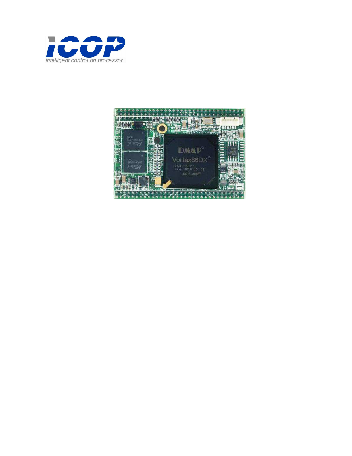
1.2 Product Description
The VDX-6319RD-FB-D family of low-power x86 embedded controller is designed to meet
Mity-SoC specification, and integrated with the following features.
800MHz Vortex86DX System-On-Chip
256MB DDR2 system memory
1 USB 2.0 (host)
Up to 2 serial ports
16-bit GPIO x1
x-ISA bus
2 watchdog timer
JTAG interface
AMI BIOS
Onboard EmbedDisk 512MB
4MB SPI flash
Single voltage +5V DC
Support extended operating
temperature range of -20°C to +70°C
The VDX-6319RD-FB-D Mity-SoC family of embedded controller is designed as the kernel of
your own application, to provide migration path for projects facing end-of-life challenges with
their existing x86 based Mity-Mite controller. The VDX-6319RD-FB-D family of controller is
designed as a plug in replacement, with backward compatibility to support legacy software to
help extend existing product life cycle without heavy re-engineering.
VDX-6319RD-FB-D is suitable for broad range of data-acquisition, Industrial automation,
Process control, Automotive controller, AVL, Intelligent Vehicle management devic,Medical
device, Human machine interface, Robotics, machinery control And more…application that
required small footprint, low-power and low-cost hardware with open industry standard such as
Mity-SoC.
Page 7
VDX-6319RD-FB-D Vortex86DX Mity-SoC CPU Module
3
1.3 Specifications
VSX-6119-1 (Mity-SoC ISA bus Development board)
Features VSX-6119-1
Bus Interfac e
16-bit x-ISA interface
PC/104 standard compliant
Status indica tor
Digit Type 7-Segment LED Display for POST Code x2
GPIO LED x16
Connectors
2.54mm 26-pin box header for Printer x1
2.54mm 20-pin box header for 16-bit GPIO x1
2.54mm 10-pin box header for RS-232 x1
2.54mm 5-pin box header for Keyboard x1
2.54mm 10-pin box header for USB x1
2.54mm 2-pin header for Reset x1
External 15-pin D-Sub female connector for VGA
External 9-pin D-Sub male connector for RS-232 x1
External Mini DIN connector for Keyboard/Mouse x1
4-pin Molex connector for Power input x1
2-pin Terminal strip for Power input x1
DC Jack for Power input x1
Power Requirement
Single Voltage +5V
@
150mA
Dimension
185 x 122mm (7.28 x 4.8 inches)
Weight
172g
Operating
Temperature
-20oC ~ +70oC
-40°C ~ +85°C (Optional)
Page 8
VDX-6319RD-FB-D Vortex86DX Mity-SoC CPU Module
4
VDX-6319RD-FB-D
Features VDX-6319RD-FB-D
CPU
DM&P SoC CPU Vortex86DX- 800MHz
Real Time Clock with Lithium Battery Backup
Cache
L1:16K I-Cache, 16K D-Cache L2:128KB Cache
BIOS
AMI BIOS
Bus Interfac e
16-bit x-ISA interface
System Memory
256MB DDR2 onboard
Watchdog Timer
Software programmable from 30.5 us to 512 seconds x2
sets(Watchdog 1 fully compatible with M6117D)
I /O Interface
RS-232 port x2 (TTLx2)
USB port (ver2.0) x1
Parallel port x1
16-bit GPIO port x1
Connectors
2.00 mm ∅ 64-pin header for 16-bit x-ISA x1
2.00 mm ∅ 64-pin header for I/O interface x1
2.00 mm ∅ 9-pin header for DMA x1
1.25mm ∅ 6-pin Wafer for JTAG x1
Flash Disk Support
Onboard 4MB SPI Flash Disk (Driver: A)
Onboard EmbedDisk 512MB (Driver: C)
Power Requirement
Single Voltage +5V
@
400mA
Dimension
65mm X 45mm (2.56 x1.77 inches)
Weight
30g
Operating
Temperature
-20oC ~ +70oC
-40°C ~ +85°C (Optional)
Page 9
VDX-6319RD-FB-D Vortex86DX Mity-SoC CPU Module
5
ICOP-6019-VGA
Features ICOP-6019-VGA
Chipset
TOPRO TP6508IQ
VGA and Mono/STN/DSTN/TFT Flat Panel interface
support
Bus
16-bit x-ISA interface
Video Memory
Onboard 1MB EDO RAM, support resolution up to
1024x768, 256 colors
Bus Interfac e
PC/104+ standard compliant
Connectors
2.0mm 44-pin box header for LCD x1
2.0mm 10-pin box header for VGA x1
2.54mm 4-pin wafer for +12V, -12V, -5V DC-in x1
Power Requirement
Single Voltage +5V@200mA
Dimension
80 x 50mm (3.14 x 1.96 inches)
Weight
32g
Operating
Temperature
-20oC ~ +60oC
Page 10
VDX-6319RD-FB-D Vortex86DX Mity-SoC CPU Module
6
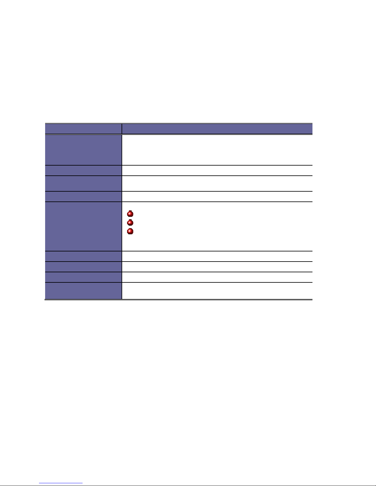
1.4 Order Selection
Page 11

VDX-6319RD-FB-D Vortex86DX Mity-SoC CPU Module
7
1.5 Board Dimension
VDX-6319RD-FB-D
Page 12
VDX-6319RD-FB-D Vortex86DX Mity-SoC CPU Module
8
C h a p t e r 2
Installation
2.1 Board Outline
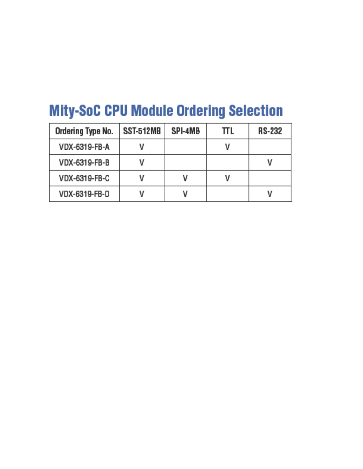
VSX-6119-1 (Mity-SoC ISA bus Development board)
Page 13
VDX-6319RD-FB-D Vortex86DX Mity-SoC CPU Module
9
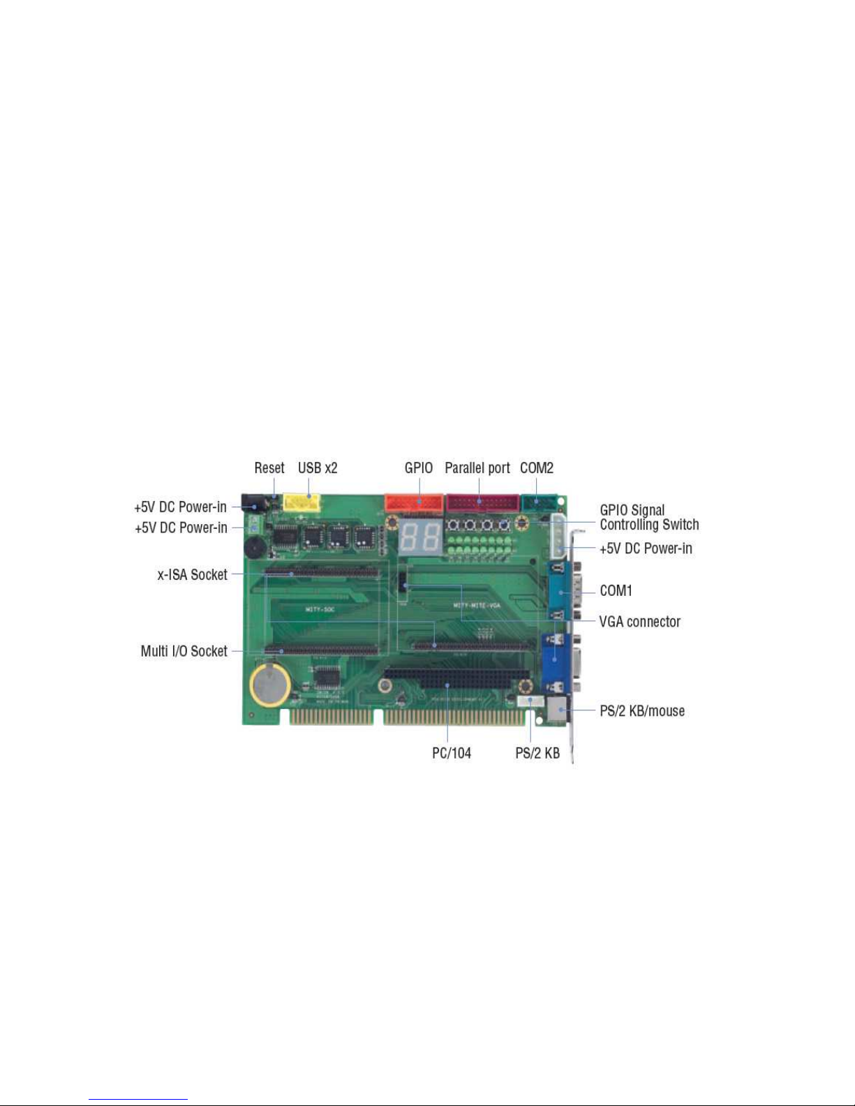
VDX-6319RD-FB-D
Note: VGA, ICOP-6019-VGA, function support via x-ISA Interface
Page 14
VDX-6319RD-FB-D Vortex86DX Mity-SoC CPU Module
10
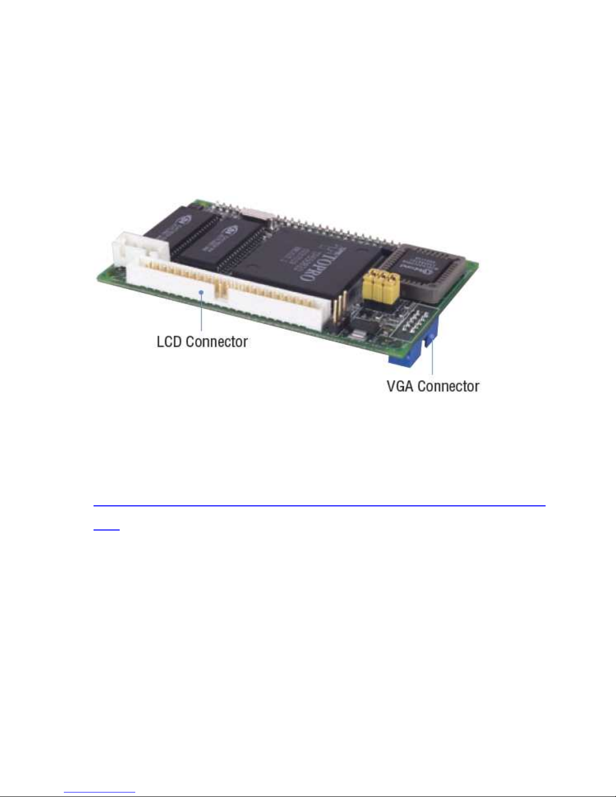
ICOP-6019-VGA
If you need more information about ICOP-6019-VGA, please visit our website at
http://www.icop.com.tw/en/product/Processor-Module-ICOP-6019-VGA/ICOP-6019-VGA
.html
Page 15
VDX-6319RD-FB-D Vortex86DX Mity-SoC CPU Module
11
2.2 Connectors & Jumpers Location
Connectors
Page 16
VDX-6319RD-FB-D Vortex86DX Mity-SoC CPU Module
12
Jumpers & LEDs
Page 17
VDX-6319RD-FB-D Vortex86DX Mity-SoC CPU Module
13
2.3 Connectors & Jumpers Summary
VSX-6119-1 (Mity-SoC ISA bus Development board)
Summary Table
Nbr Description Type of Connections Pin nbrs.
J1 x-ISA Connector – 64 pin Box Header, 2.0∅, 32x2 64-pin
J2 ISA bus Connector, SL62 62-pin Gold finger 62-pin
J3 ISA bus Connector, SL36 36-pin Gold finger 36-pin
J4 PC104 Connector – 64 pin Box Header, 2.54∅ ,32x2
64-pin
J5 PC104 Connector – 40 pin Box Header, 2.54∅ ,20x2
40-pin
J6 Mity-Mite VGA Connector Box Header, 2.0∅, 32x2 64-pin
J7 USB Pin Header, 2,54∅,5x2 10-pin
J8 Multi I/O Connector – 64 pin
Box Header, 2.0∅, 32x2 64-pin
J9 GPIO Port Box Header, 2.54∅ ,10x2
20-pin
J10 COM1 D-Sub Connector 9-pin
J11 COM2 Box Header, 2.54∅, 5x2 10-pin
J12 Reset Pin Header, 2.54∅, 1x2 2-pin
J13 PS/2 Keyboard Box Header,2.54∅, 1x5 5-pin
J14 VGA D-Sub female connector 15-pin
J15 Power Connector Terminal Block 5.0∅ , 2x1
2-pin
J16 Power Connector DC -JACK 3-pin
J17
Power Connector Box Header, 5.0∅ Molex
4-pin
J18 VGA connector Box Header, 2.54∅ , 5x2
10-pin
J19 PS/2 Keyboard Mini-Din Connector 9-pin
J20 PRINT Box Header, 2.54∅ ,13x2
26-pin
S1~S4 Switch Input
U5 80 PORT (7Segment Display)
18-pin DIP SSD 18-pin
SP1 BUZZER
GP0~GP15 LED Display
Page 18

VDX-6319RD-FB-D Vortex86DX Mity-SoC CPU Module
14
2.4 Pin Assignments & Jumper Settings
VSX-6119-1 (Mity-SoC ISA bus Development board)
J1: x-ISA Connector – 64pin
Pin # Signal Name Pin # Signal Name
1 GND
2
SBHE
3 RSTDRV
4
SD7
5 VCC
6
SD6
7 SD8
8
SD5
9 SD9
10
SD4
11 SD10
12
SD3
13 SD11
14
SD2
15 SD12
16
SD1
17 SD13
18
SD0
19 GND
20 IOCHRDY
21 SMEMW
22
AEN
23 SMEMR
24
SA19
25 IOW
26
SA18
27 IOR
28
SA17
29 SD14
30
SA16
31 SD15
32
SA15
33 MEMCS16
34
SA14
35 ICOS16
36
SA13
37 REFRESH
38
SA12
39 SYSCLK
40
SA11
41 IRQ7
42
SA10
43 IRQ6
44
SA9
45 IRQ5
46
SA8
47 IRQ4
48
SA7
49 I
RQ3
50
SA6
51 IRQ10
52
SA5
53 IRQ11
54
SA4
55 BALE
56
SA3
57 VCC
58
SA2
59 OSC
60
SA1
61 GND
62
SA0
63 IRQ12
64
IRQ14
Page 19

VDX-6319RD-FB-D Vortex86DX Mity-SoC CPU Module
15
J2: ISA Bus SL62 – 62-pin Gold finger (Total 98 pins)
Pin # Signal Name Pin #
Signal
Name
1 (A1)
IOCHCK
2 (B1)
GND
3 SD7
4 RSTDRV
5
SD6
6 VCC
7
SD5
8 IRQ9
9
SD4
10 -5V
11
SD3
12 DRQ2
13
SD2
14 -
12V
15
SD1
16 OWS
17
SD0
18 +12V
19 IOCHRDY
20
GND
21 AEN
22
SMEMW
23 SA19
24
SMEMR
25 SA18
26
IOW
27 SA17
28
IOR
29 SA16
30
DACK3
31 SA15
32
DRQ3
33 SA14
34
DACK1
35 SA13
36
DRQ1
37 SA12
38
REFRESH
39 SA11
40
SYSCLK
41 SA10
42
IRQ7
43 SA9
44
IRQ6
45 SA8
46
IRQ5
47 SA7
48
IRQ4
49 SA6
50
IRQ3
51 SA5
52
DACK2
53 SA4
54 TC
55 SA3
56
BALE
57 SA2
58
VCC
59 SA1
60
OSC
61 SA0
62
GND
Page 20

VDX-6319RD-FB-D Vortex86DX Mity-SoC CPU Module
16
J3: ISA bus SL36 – 36-pin Gold finger (Total 98 pins)
Pin # Signal Name Pin #
Signal
Name
1 (A1)
SBHE
2 (B1)
MEMCS16
3 LA23
4
IOCS16
5 LA22
6
IRQ10
7 LA21
8
IRQ11
9 LA20
10
IRQ12
11 LA19
12
IRQ15
13 LA18
14
IRQ14
15 LA17
16
DACK0
17 MEMR
18
DRQ0
19 MEMW
20
DACK5
21 SD8
22 DRQ5
23 SD9
24
DACK6
25 SD10
26
DRQ6
27 SD11
28
DACK7
29 SD12
30
DRQ7
31 SD13
32
VCC
33 SD14
34
MASTER
35 SD15
36
GND
Page 21

VDX-6319RD-FB-D Vortex86DX Mity-SoC CPU Module
17
J4: PC104 Connector – 64pin
Pin # Signal Name Pin # Signal Name
1 IOCHCHK
*
2 GND
3 SD7
4
RESETDRV
5 SD6
6
VCC
7 SD5
8 IRQ9
9 SD4
10 -5V
11 SD3
12 DRQ2
13 SD2
14 -12V
15 SD1
16
OWS
17 SD0
18
+12V
19 IOCHRDY
20
GND
21 AEN
22
SMEMW *
23 SA19
24
SMEMR *
25 SA18
26
IOW *
27 SA17
28
IOR *
29 SA16
30
DACK3 *
31 SA15
32
DRQ3
33 SA14
34
DACK1 *
35 SA13
36
DRQ1
37 SA12 38
REFRESH *
39 SA11
40
SYSCLK
41 SA10
42
IRQ7
43 SA9
44
IRQ6
45 SA8
46
IRQ5
47 SA7
48
IRQ4
49 SA6
50
IRQ3
51 SA5
52
DACK2 *
53 SA4
54 TC
55 SA3
56
BALE
57 SA2
58
VCC
59 SA1
60
OSC
61 SA0
62
GND
63 GND
64
GND
Page 22

VDX-6319RD-FB-D Vortex86DX Mity-SoC CPU Module
18
J5: PC104 Connector – 40pin
Pin # Signal Name Pin # Signal Name
1 GND
2
GND
3 MEMCS16 *
4
SBHE *
5 IOCS16 *
6
SA23
7 IRQ10
8
SA22
9 IRQ11
10
SA21
11 IRQ12
12
SA20
13 IRQ15
14
SA19
15 IRQ14
16
SA18
17 DACK0 *
18
SA17
19 DRQ0
20
MEMR *
21 DACK5 *
22
MEMW *
23 DRQ5
24
SD8
25 DACK6 *
26
SD9
27 DRQ6
28
SD10
29 DACK7 *
30
SD11
31 DRQ7
32
SD12
33 VCC
34
SD13
35 MASTER *
36
SD14
37 GND
38
SD15
39 GND
40 NC
Page 23

VDX-6319RD-FB-D Vortex86DX Mity-SoC CPU Module
19
J6: Mity-Mite VGA Connector
Pin # Signal Name Pin # Signal Name
1 GND
2
SBHE
3 RSTDRV
4
SD7
5 VCC
6
SD6
7 SD8
8
SD5
9 SD9
10
SD4
11 SD10
12
SD3
13 SD11
14
SD2
15 SD12
16
SD1
17 SD13
18
SD0
19 GND
20
IOCHRDY
21 SMEMW
22
AEN
23 SMEMR
24
SA19
25 XIOW
26
SA18
27 XIOR
28
SA17
29 SD14
30
SA16
31 SD15
32
SA15
33 MEMCS16
34
SA14
35 TOCS16
36 SA13
37 REFRESH
38
SA12
39 SYSCLK
40
SA11
41 IRQ7
42
SA10
43 IRQ6
44
SA9
45 IRQ5
46
SA8
47 IRQ4
48
SA7
49 IRQ3
50
SA6
51 IRQ10
52
SA5
53 IRQ11
54
SA4
55 BALE
56
SA3
57 VCC
58
SA2
59 XOSC
60
SA1
61 GND
62
SA0
63 IRQ12
64
IRQ14
Page 24

VDX-6319RD-FB-D Vortex86DX Mity-SoC CPU Module
20
J7: USB
Pin # Signal Name Pin # Signal Name
1 VCC
2
VCC
3 LUSBD
0- 4
LUSBD
1-
5 LUSBD
0+ 6 LUSBD
1+
7 GND
8
GND
9 G
GND
10 GGND
J8: I /O Connector – 64pin
Pin # Signal Name Pin # Signal Name
1 DCD1
2
RXD1
3 TXD1
4
DTR1
5 GND
6
DSR1
7 RTS1
8
CTS1
9 RI1 10 VCC
11 DCD2
12
RX2
13 TXD2
14
DTR2
15 GND
16
DSR2
17 RTS2
18
CTS2
19 RI2 20 VCC
21 PD0
22
SLCT
23 PD1
24 PR
25 PD2
26
BUSY
27 PD3
28
ACK
\
29 PD4
30
SLCTIN
\
31 PD5
32
INIT
\
33 PD6
34
ERROR
\
35 PD7
36
AUTOFD
\
37 GND
38
STORBE
\
39 GP0
40
GP8
41 GP1
42
GP9
43 GP2
44
GP10
45 GP3
46
GP11
47 GP4
48
GP12
49 GP5
50
GP13
51 GP6
52
GP14
53 GP7
54
GP15
55 GPCS0
56
VBAT
57 KBDAT
58
HDCS0
59 KBCLK
60
HDCS1
61 SPKR
62
RESETL
63 GND
64
PWG
Page 25

VDX-6319RD-FB-D Vortex86DX Mity-SoC CPU Module
21
J9: GPIO
J10: COM 1
Pin #
Signal
Name
Pin #
Signal
Name
1 DCD1
2 RXD1
3 TXD1
4 DTR1
5 GND 6 DSR1
7 RTS1
8 CTS1
9 RI1 10 GND
11 GND
J11: COM 2
Pin # Signal Name Pin # Signal Name
1 DCD2 2 RXD2
3 TXD2 4 DTR2
5 GND 6 DSR2
7 RTS2 8 CTS2
9 RI2 10
NC
Pin # Signal Name Pin # Signal Name
1 GND 2 VCC
3 GP00 4 GP10
5 GP01 6 GP11
7 GP02 8 GP12
9 GP03 10
GP13
11 GP04 12
GP14
13 GP05 14
GP15
15 GP06 16
GP16
17 GP07 18
GP17
19 VCC 20
GND
Page 26

VDX-6319RD-FB-D Vortex86DX Mity-SoC CPU Module
22
J12: RESET
Pin # Signal Name Pin # Signal Name
1 Reset 2 GND
J13: PS/2 Keyboard
Pin # Signal Name Pin # Signal Name
1 KBCLK
2
KBDAT
3 NC 4 GND
5 VCC
J14: VGA
Pin # Signal Name Pin # Signal Name
1 R OUT 2 G OUT
3 B OUT 4 NC
5 GND 6 GND
7 GND 8 GND
9 VCC 10
GND
11 NC 12
DDCDAT
13 HSYNC 14
VSYNC
15 DDCCLK
J15: Power Connector (Terminal Block 5.0mm)
Pin # Signal Name
1 +5V
2 GND
J16: Power Connector (DC-JACK)
Pin # Signal Name
1 +5V
2 GND
3 NC
Page 27

VDX-6319RD-FB-D Vortex86DX Mity-SoC CPU Module
23
J17: Power Connector – 4-pin Header (P4 Molex 5mm)
Pin #
Signal
Name
1 +5V
2 GND
3 GND
4 +12V
J18: VGA
Pin #
Signal
Name
Pin #
Signal
Name
1 R OUT
2 GND
3 G OUT
4 GND
5 B OUT
6 GND
7 HSYNC
8 GND
9 VSYNC
10 GND
J19: PS/2 Keyboard / Mouse
Pin # Signal Name Pin # Signal Name
1 KBDATA 2 NC
3 GND 4 VCC
5 KBCLK 6 NC
7 MSDATA 8 NC
9 GND 10
VCC
11 MSCLK 12
NC
13 GGND 14
GGND
15 GGND 16
GGND
17 GGND
Page 28

VDX-6319RD-FB-D Vortex86DX Mity-SoC CPU Module
24
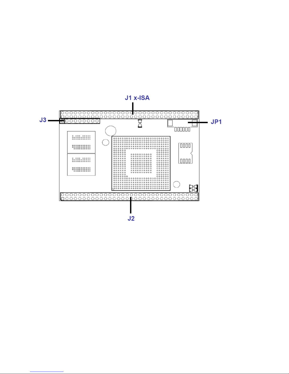
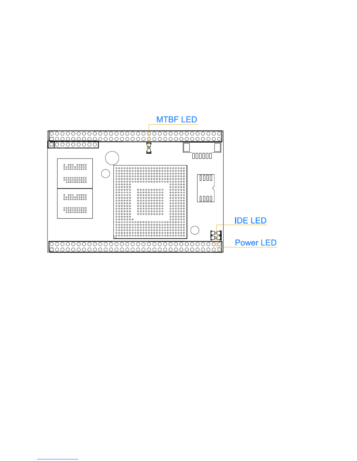
VDX-6319RD-FB-D
Summary Table
Nbr Description Type of Connections Pin nbrs.
J1 x-ISA Connector – 64 pin Pin Header, 2.0∅, 32x2 64-pin
J2 Multi I/O Connector – 64 pin Pin Header, 2.0∅, 32x2 64-pin
J3 DMA control Pin Header, 2,0∅,1x9 9-pin
JP1 JTAG Wafer, 1.25∅ , 6x1 6-pin
PWR-LED Power Active LED (Red) LED-SMD
MTBF-
LED
MTBF-Out (Orange) LED-SMD
Page 29

VDX-6319RD-FB-D Vortex86DX Mity-SoC CPU Module
25
J1: x-ISA Connector – 64pin
Pin # Signal Name Pin # Signal Name
1 GND
2
SBHE
3 RSTDRV
4
SD7
5 VCC
6 SD6
7 SD8
8
SD5
9 SD9
10
SD4
11 SD10
12
SD3
13 SD11
14
SD2
15 SD12
16
SD1
17 SD13
18
SD0
19 GND
20
IOCHRDY
21 SMEMW
22
AEN
23 SMEMR
24
SA19
25 IOW
26
SA18
27 IOR
28
SA17
29 SD14
30
SA16
31 SD15
32
SA15
33 MEMCS16
34
SA14
35 ICOS16
36
SA13
37 REFRESH
38
SA12
39 SYSCLK
40
SA11
41 IRQ7
42
SA10
43 IRQ6
44
SA9
45 IRQ5
46
SA8
47 IRQ4
48
SA7
49 IRQ3
50
SA6
51 IRQ10
52
SA5
53 IRQ11
54
SA4
55 BALE
56
SA3
57 VCC
58
SA2
59 OSC
60
SA1
61 GND
62
SA0
63 IRQ12
64
IRQ14
Page 30

VDX-6319RD-FB-D Vortex86DX Mity-SoC CPU Module
26
J2: I /O Connector – 64pin
Pin # Signal Name Pin # Signal Name
1 DCD1
2
RXD1
3 TXD1
4
DTR1
5 GND
6
DSR1
7 RTS1
8
CTS1
9 RI1 10 VCC
11 DCD2
12
RX2
13 TXD2
14
DTR2
15 GND
16
DSR2
17 RTS2
18
CTS2
19 RI2 20 VCC
21 PD0
22
SLCT
23 PD1
24 PR
25 PD2
26
BUSY
27 PD3
28
ACK
\
29 PD4
30
SLCTIN
\
31 PD5
32
INIT
\
33 PD6
34
ERROR
\
35 PD7
36
AUTOFD
\
37 GND
38
STORBE
\
39 GP0
40
GP8
41 GP1
42
GP9
43 GP2
44
GP10
45 GP3
46
GP11
47 GP4
48
GP12
49 GP5
50
GP13
51 GP6
52
GP14
53 GP7
54
GP15
55 GPCS0
56
VBAT
57 KBDAT
58
HDCS0
59 KBCLK
60
HDCS1
61 SPKR
62
RESETL
63 GND
64
PWG
J3: DMA control
Pin # Signal Name Pin # Signal Name
1 40MHZ 2 GND
3 DACK1 4 DACK3
5 DRQ1 6 DRQ3
7 TC 8 MEMR
9 MEMW
Page 31

VDX-6319RD-FB-D Vortex86DX Mity-SoC CPU Module
27
JP1: JTAG
Pin # Signal Name Pin # Signal Name
1 VCC 2 GND
3 TCK 4 TDO
5 TDI 6 TMS
Page 32

VDX-6319RD-FB-D Vortex86DX Mity-SoC CPU Module
28
2.5 System Mapping
Page 33

VDX-6319RD-FB-D Vortex86DX Mity-SoC CPU Module
29
Page 34

VDX-6319RD-FB-D Vortex86DX Mity-SoC CPU Module
30
Page 35

VDX-6319RD-FB-D Vortex86DX Mity-SoC CPU Module
31
2.6 Watchdog Timer
There are two watchdog timers in Vortex86SX/DX CPU. One is compatible with M6117D
watchdog timer and the other is new. The M6117D compatible watchdog timer is called WDT0
and new one is called WDT1.
We also provide DOS, Linux and WinCE example for your reference. For more technical support,
please visit: http://www.dmp.com.tw/tech or download the PDF file:
http://www.dmp.com.tw/tech/vortex86dx/
Page 36

VDX-6319RD-FB-D Vortex86DX Mity-SoC CPU Module
32
2.7 GPIO (General Purpose Input / Output)
40 GPIO pins are provided by the Vortex86SX/DX for general usage in the system. All GPIO pins
are independent and can be configured as inputs or outputs, with or without pull-up/pull-down
resistors.
We also offer DOS, Linux and WinCE example for your reference. For more technical support,
please visit: http://www.dmp.com.tw/tech or download the PDF file:
http://www.dmp.com.tw/tech/vortex86dx/
Page 37

VDX-6319RD-FB-D Vortex86DX Mity-SoC CPU Module
33
2.8 SPI flash (Serial Peripheral Interface)
As SPI Flash (Serial Peripheral Interface) offers many benefits including: reduced controller pin
count, smaller and simpler PCBs, reduced switching noise, less power consumption, and lower
system cost
Many of users may consider using a formatted SPI flash to boot for the system or emulate SPI
flash as Floppy (A: Driver or B: Driver). Then you must know how to set for this condition in
CMOS Setup and boot up under DOS 6.22, X-DOS, DR-DOS and Free DOS.
For more technical support, please visit: http://www.dmp.com.tw/tech or download the PDF file:
http://www.dmp.com.tw/tech/vortex86sx/
Page 38

VDX-6319RD-FB-D Vortex86DX Mity-SoC CPU Module
34
C h a p t e r 3
SVGA Setup
(For ICOP-6019-VGA / LCD Module)
3.1 Introduction
The ICOP-6019-VGA has an on-board VGA interface. The specifications and features are
described as follows or please visit our website:
http://www.icop.com.tw/pddetail.aspx?id=47&pid=4
3.1.1 Chipset
The ICOP-6019-VGA uses a HMC HM86508 for its SVGA controller, which supports conventional
analog CRT monitor or flat panel. In addition, it also supports interlaced and non-interlaced
analog monitors (color and monochrome VGA) in high-resolution modes while maintaining
complete IBM VGA compatibility. Multiple frequency (multisync) monitors are handled as if they
were analog monitors.
3.1.2 Display memory
With 1 MB memory, the VGA controller can drive CRT displays or color panel displays with
resolutions up to 1024 x 768 at 256 colors.
Page 39

VDX-6319RD-FB-D Vortex86DX Mity-SoC CPU Module
35
3.2 Flat Panel Connectors
Flat Panel Pin Assignment
Pin
Description Pin Description
1 +12V 2 +12V
3 GND 4 GND
5 PVcc 6 PVcc
7 ENAVEE 8 ENAVEE
9 P0 10 P1
11 P2 12 P3
13 P4 14 P5
15 P6 16 P7
17 P8 18 P9
19 P10 20 P11
21 P12 22 P13
23 P14 24 P15
25 P16 26 P17
27 P18 28 P19
29 P20 30 P21
31 P22 32 P23
33 GND 34 GND
35 SHFCLK 36 FLM
37 M 38 LP
39 GND 40 ENABKL
41 GND 42 ASHFCLK
43 Vcc 44 Vcc
Page 40

VDX-6319RD-FB-D Vortex86DX Mity-SoC CPU Module
36
Description for the Pin of the Flat Panel Connector
Name Description
P0~P23 Flat panel data output
ENABKL Activity Indicator and Enable Backlight outputs
SHFCLK Shift clock. Pixel clock for flat panel data
M M signal for panel AC drive control
LP Latch pulse. Flat panel equivalent of HSYNC
FLM First line marker. Flat panel equivalent of VSYNC
+12V +12V power from PC power supply
ENAVDD Power sequencing controls for panel LCD bias volt
ENAVEE Power sequencing controls for panel LCD bias volt
–SHFCLK The inverter signal of SHFCLK
VDDM 3.3V or 5V selected by JP6
Page 41

VDX-6319RD-FB-D Vortex86DX Mity-SoC CPU Module
37
3.3 Flat Panel Jumper setting
J1: LCD Type Select
Type of Display 1-2 3-4 5-6 Address of VGA BIOS
1
Standard CRT C C C
00000~07FFF Hex
2
Mono DSTN 640x480 C C O
08000~0FFFF Hex
3
Color DSTN 640x480
C
O C
10000~17FFF Hex
4
16-bit TFT 640x480 C O O
18000~1FFFF Hex
5
18/24-bit TFT 640x480 O C C
20000~27FFF Hex
6
16-bit TFT 800x600 O C O
28000~2FFFF Hex
7
18/24-bit TFT 800x600 O O C
30000~37FFF Hex
8
EL 640x480 O O O
38000~3FFFF Hex
Note: “C” means “close”; “O” means “open”
J3: LCD voltage select
Voltage
Pin1-2 Pin 2-3
5V close
3.3V close
Page 42

VDX-6319RD-FB-D Vortex86DX Mity-SoC CPU Module
38
3.4 Flat Panel BIOS and Wiring
Below is a list of optional Flat Panel SVGA BIOS. The VGA BIOS is combined with the system
BIOS in a single. To change to another BIOS please contact your local dealer.
MLCD.dat - Data File for MONO DSTN640*480 (Default)
Example: (1) HOSIDEN HLM6667
(2) HITACHI LMG5160XUFC
(3) CASIO MD650TS00-01
(4) OPTREX DMF_50260NFU-FW-8
DSTN.dat - Data file for Color DSTN640*480
Example: (1) Sanyo LCM-5331-22NTK
(2) SHARP LM64C35P
TFT_S1.dat - Data File for TFT640*480-Sync (16 BIT)
TFT_S2.dat - Data File for TFT640*480-Sync (18/24 BIT)
Example: (1) HITACHI TX26D60/TX24D55
(2) TOSHIBA LTM09C015A
(3) SHARP LQ10D321
TFT_LP1.dat - Data File For TFT640*480-LP (16 BIT)
TFT_LP2.dat - Data File For TFT640*480-LP (18/24 BIT)
Example: (1) Toshiba LTM09c015A)
TFT86_S1.dat - Data File for TFT800*600_sync (16 BIT)
TFT86_S2.dat Data File for TFT800*600_sync (18/24 BIT)
Example: (1) NEC NL8060AC26-05
(2) NEC NL8060AC26-04
(3) NEC NL8060BC31-02
EL.dat - Data File for EL640*480
Example: (1) PLANAR EL640.480-A
PLASMA.dat - Data File for PLASMA640*480
Example: (1) PANASONIC S817
Page 43

VDX-6319RD-FB-D Vortex86DX Mity-SoC CPU Module
39
CRT / Flat Panel Mode
All the above BIOS support either CRT only, Flat Panel only or CRT/Flat Panel simultaneously.
To set the mode a Panel Switching Utility is used.
USAGE:
At DOS prompt type >SW508 then Screen will show
1. CRT Only
2. Panel Only
3. CRT/Panel Simutaneous
Page 44

VDX-6319RD-FB-D Vortex86DX Mity-SoC CPU Module
40
NEC NL6448AC33-18 wiring
NEC NL6448AC33-18 ICOP-2820V CON1
Pin Pin Name Pin Pin Name
CN1-1 GND 3 GND
CN1-2 CLK 35 SHFCLK
CN1-3 Hsync 38 LP
CN1-4 Vsync 36 FLM
CN1-5 GND 4 CN1-6 R0 27 P18
CN1-7 R1 28 P19
CN1-8 R2 29 P20
CN1-9 R3 30 P21
CN1-10 R4 31 P22
CN1-11 R5 32 P23
CN1-12 GND 33 CN1-13 G0 19 P10
CN1-14 G1 20 P11
CN1-15 G2 21 P12
CN1-16 G3 22 P13
CN1-17 G4 23 P14
CN1-18 G5 24 P15
CN1-19 GND 34 CN1-20 B0 11 P2
CN1-21 B1 12 P3
CN1-22 B2 13 P4
Page 45

VDX-6319RD-FB-D Vortex86DX Mity-SoC CPU Module
41
CN1-23 B3 14 P5
CN1-24 B4 15 P6
CN1-25 B5 16 P7
CN1-26 GND 39 CN1-27 ENAB 37 MDE
CN1-28 Vcc 43 Vcc
CN1-29 Vcc 44 Vcc
CN1-30 NC - CN1-31 NC - -
NEC NL6448AC30-10 wiring
NEC NL6448AC30-10 ICOP-2820V CON1
Pin Pin Name Pin Pin Name
CN1-1 CLK 42 SHFCLK
CN1-2 Hsync 38 LP
CN1-3 Vsync 36 FLM
CN1-4 DE 37 MDE
CN1-5 - - P0
CN1-6 B0 10 P1
CN1-7 B1 11 P2
CN1-8 B2 12 P3
CN1-9 B3 13 P4
CN1-10 - 14 P5
CN1-11 - 15 P6
CN1-12 G0 16 P7
Page 46

VDX-6319RD-FB-D Vortex86DX Mity-SoC CPU Module
42
CN1-13 G1 17 P8
CN1-14 G2 18 P9
CN1-15 G3 19 P10
CN1-16 - 20 P11
CN1-17 R0 21 P12
CN1-18 R1 22 P13
CN1-19 R2 23 P14
CN1-20 R3 24 P15
CN1-21 - - P16
CN1-22 - - P17
CN1-23 - 27 P18
CN1-24 - 28 P19
CN1-25 - 29 P20
CN1-26 - 30 P21
CN1-27 - 31 P22
CN1-28 - 32 P23
CN1-29 PVcc 5 LCD Vdd
CN1-30 Vcc 43 Vcc
CN1-31 MODE 44 Vcc
CN1-32 GND 3 GND
CN1-33 GND 4 GND
CN1-34 Vdd +12 1 +12
CN1-35 ENABKL 40 ENABKL
CN1-36 GND 39 GND
Page 47

VDX-6319RD-FB-D Vortex86DX Mity-SoC CPU Module
43
LJ32H028 wiring
LJ32H028 ICOP-2820V CON1
Pin Pin Name Pin Pin Name
CN1-1 D1 11 P2
CN1-2 D0 12 P3
CN1-3 D3 9 P0
CN1-4 D2 10 P1
CN1-5 CP2 35 SHF_CLK
CN1-6 GND 3,4 GND
CN1-7 CP1 38 LP
CN1-8 GND 33,34 GND
CN1-9 S 36 FLM
CN1-10 - - CN1-11 - - CN1-12 - - CN1-13 +5V 43,44 +5V(Vdd)
CN1-14 - - CN1-15 +12V 1,2 +12V
SHARP LQ10D42 wiring
(640 X 480 TFT Color)
SHARP LQ10D42 ICOP-2820V CON1
Pin Pin Name Pin Pin Name
CN1-1 GND 3,4 GND
Page 48

VDX-6319RD-FB-D Vortex86DX Mity-SoC CPU Module
44
CN1-2 CLK 42 SHFCLK
CN1-3 Hsync 38 LP
CN1-4 Vsync 36 FLM
CN1-5 GND 3,4 GND
CN1-6 R0 21 P12
CN1-7 R1 22 P13
CN1-8 R2 23 P14
CN1-9 R3 24 P15
CN1-10 R4 25 P16
CN1-11 R5 26 P17
CN1-12 GND 3,4 GND
CN1-13 G0 15 P6
CN1-14 G1 16 P7
CN1-15 G2 17 P8
CN1-16 G3 18 P9
CN1-17 G4 19 P10
CN1-18 G5 20 P11
CN1-19 GND 3,4 GND
CN1-20 B0 9 P0
CN1-21 B1 10 P1
CN1-22 B2 11 P2
CN1-23 B3 12 P3
CN1-24 B4 13 P4
CN1-25 B5 14 P5
CN1-26 GND 3,4 GND
CN1-27 ENAB 40 M
Page 49

VDX-6319RD-FB-D Vortex86DX Mity-SoC CPU Module
45
CN1-28 Vcc 43,44 Vcc +5V
CN1-29 Vcc 43,44 Vcc +5V
CN1-30 R/L - CN1-31 U/D - -
SHARP LQ12S31 wiring
(800 X 600 TFT Color)
SHARP LQ12S31 ICOP-2820V CON1
Pin Pin Name Pin Pin Name
CN1-1 GND 3 GND
CN1-2 CLK 35 SHFCLK
CN1-3 GND 4 GND
CN1-4 Hsync 38 LP
CN1-5 Vsync 36 FLM
CN1-6 GND 8 GND
CN1-7 GND 8 GND
CN1-8 GND 8 GND
CN1-9 R0 27 P18
CN1-10 R1 28 P19
CN1-11 R2 29 P20
CN1-12 GND 8 GND
CN1-13 R3 30 P21
CN1-14 R4 31 P22
CN1-15 R5 32 P23
CN1-16 GND 39 GND
Page 50

VDX-6319RD-FB-D Vortex86DX Mity-SoC CPU Module
46
CN1-17 GND 39 GND
CN1-18 GND 39 GND
CN1-19 G0 19 P10
CN1-20 G1 20 P11
CN1-21 G2 21 P12
CN1-22 GND 39
CN1-23 G3 22 P13
CN1-24 G4 23 P14
CN1-25 G5 24 P15
CN1-26 GND 41 GND
CN1-27 GND 41 GND
CN1-28 GND 41 GND
CN1-29 B0 11 P2
CN1-30 B1 12 P3
CN1-31 B2 13 P4
CN1-32 GND 41 GND
CN1-33 B3 14 P5
CN1-34 B4 15 P6
CN1-35 B5 16 P7
CN1-36 GND 41 GND
CN1-37 ENAR 37 M
CN1-38 TST - CN1-39 Vcc 43 +5Vcc
CN1-40 Vcc 44 +5Vcc
CN1-41 TST - -
Page 51

VDX-6319RD-FB-D Vortex86DX Mity-SoC CPU Module
47
C h a p t e r 4
Driver Installation
LAN
The Vortex86DX processor also integrated 10/100Mbps Ethernet controller that supports both
10/100BASE-T and allows direct connection to your 10/100Mbps Ethernet based Local Area
Network for full interaction with local servers, wide area networks such as the Internet.
The controller supports: Half / Full-Duplex Ethernet function to double channel bandwidth, auto
media detection.
Operating system support
The VDX-6319RD-FB-D Mity-SoC CPU board supports Embedded software: Free DOS, DOS
6.22, PCDOS 7.1, DR-DOS,x-DOS,OS/2,Windows CE 6.0, Windows 98, Windows XP
Professional, Windows Embedded standard (XPE) and Windows 2000 (SP4)
Please get the drivers from the Driver CD which attached with the standard packing of
VDX-6319RD-FB-D board or please get it from DMP official website:
http://www.dmp.com.tw/tech/vortex86dx/
VDX-6319RD-FB-D also supports most of the popular Linux distributions, for more detail
information, please visit DMP official website: http://www.dmp.com.tw/tech/vortex86dx/
Page 52

VDX-6319RD-FB-D Vortex86DX Mity-SoC CPU Module
48
Appendix
A. TCP/IP library for DOS real mode
DSock is a TCP/IP library for DOS real mode, which is used by RSIP. It provides simple C
functions for programmer to write Internet applications. ICOP also provide Internet examples
using DSock: BOOTP/DHCP, FTP server, SMTP client/server, HTTP server, TELNET server,
Talk client/server, etc.
DSock provides a lot of example source code. Programmer can add Internet functions to their
project easily and save development time. With a utility "MakeROM”, programmer also can make
a ROM image to fit their application, those examples can be seen in the following Application
systems: Mity-Mite Serial Server, Web Camera Tiny Server and RSIP Serial Server.
DSock is free for All ICOP products using M6117D/Vortex86/Vortex86SX/Vortex86DX CPU and
ICOP also provide the business version of DSock for those customers who are using other x86
CPUs.
If you would like to use DSock or business version of DSock, Please mail to info@icop.com.tw or
contact your regional sales.
Please download the trial DSock software and Utilities from our website:
http://www.dmp.com.tw/tech/dmp-lib/dsock/
Page 53

VDX-6319RD-FB-D Vortex86DX Mity-SoC CPU Module
49
B. VDX-6319RD-FB-D & VSX-6119-1 Schematic
Schematic information can help baseboard designer to optimize exactly how each of these
functions implements physically. Designer can place connectors precisely where needed for the
application on a baseboard designed to optimally fit a system’s packaging.
Please contact or e-mail our regional sales to get VDX-6319RD-FB-D & VSX-6119-1 Schematic.
Page 54

VDX-6319RD-FB-D Vortex86DX Mity-SoC CPU Module
50
Warranty
This product is warranted to be in good working order for a period of one year from the date of
purchase. Should this product fail to be in good working order at any time during this period, we
will, at our option, replace or repair it at no additional charge except as set forth in the following
terms. This warranty does not apply to products damaged by misuse, modifications, accident or
disaster. Vendor assumes no liability for any damages, lost profits, lost savings or any other
incidental or consequential damage resulting from the use, misuse of, originality to use this
product. Vendor will not be liable for any claim made by any other related party. Return
authorization must be obtained from the vendor before returned merchandise will be accepted.
Authorization can be obtained by calling or faxing the vendor and requesting a Return
Merchandise Authorization (RMA) number. Returned goods should always be accompanied by a
clear problem description.
 Loading...