

ICOP VDX-6319D-FB-D, VDX-6319RD-FB-D User Manual
Mity-SoC Development Kit
&
Mity-SoC CPU Module
with 2S/USB/GPIO 256MB DDR2 Onboard
(Onboard EmbedDisk 512MB)
User’s Manual
(Revision 1.1A)

Copyright
The information in this manual is subject to change without notice for continuous improvement in
the product. All rights are reserved. The manufacturer assumes no responsibility for any
inaccuracies that may be contained in this document and makes no commitment to update or to
keep current the information contained in this manual.
No part of this manual may be reproduced, copied, translated or transmitted, in whole or in part,
in any form or by any means without the prior written permission of the ICOP Technology Inc.
Copyright 2008 ICOP Technology Inc.
Manual No. IUM6319D-FB-D000-01 Ver.1.0A December, 2010
Manual No. IUM6319RD-FB-D000-01 Ver.1.1A September, 2014
Trademarks Acknowledgment
Vortex86DX is the registered trademark of ICOP Technology Inc.
Other brand names or product names appearing in this document are the properties
and registered trademarks of their respective owners. All names mentioned herewith
are served for identification purpose only.

T a b l e o f C o n t e n t s
T a b l e o f C o n t e n t s ............................................................. iii
C h a p t e r 1 Introduction……………………………………………1
1.1 Packing List ............................................................ 1
1.2 Product Description ................................................ 2
1.3 Specifications ......................................................... 3
1.4 Order Selection ...................................................... 6
1.5 Board Dimension .................................................... 7
C h a p t e r 2 Installation……………………………………………..8
2.1 Board Outline ......................................................... 8
2.2 Connectors & Jumpers Location ................... ........11
2.3 Connectors & Jumpers Summary ......................... 13
2.4 Pin Assignments & Jumper Settings ..................... 14
2.5 System Mapping ................................................... 28
2.6 Watchdog Timer ................................................... 31
2.7 GPIO .................................................................... 32
2.8 SPI flash ............................................................... 33
C h a p t e r 3 SVGA Setup.......…………………………………….34
3.1 Introduction .......................................................... 34
3.2 Flat Panel Pin Assignment.................................... 35
3.3 Flat Panel Jumper Settings .................................. 37
3.4 Flat Panel BIOS and Wiring.................................. 38
C h a p t e r 4 Driver Installation……………………………………47
Appendix ………………………………………………………………..48
A. TCP/IP library for DOS real mode ............................. 48
B. VDX-6319D-FB-D & VSX-6119-1 Schematic ............ 49
Warranty ............................................................................................ 50

This page is blank
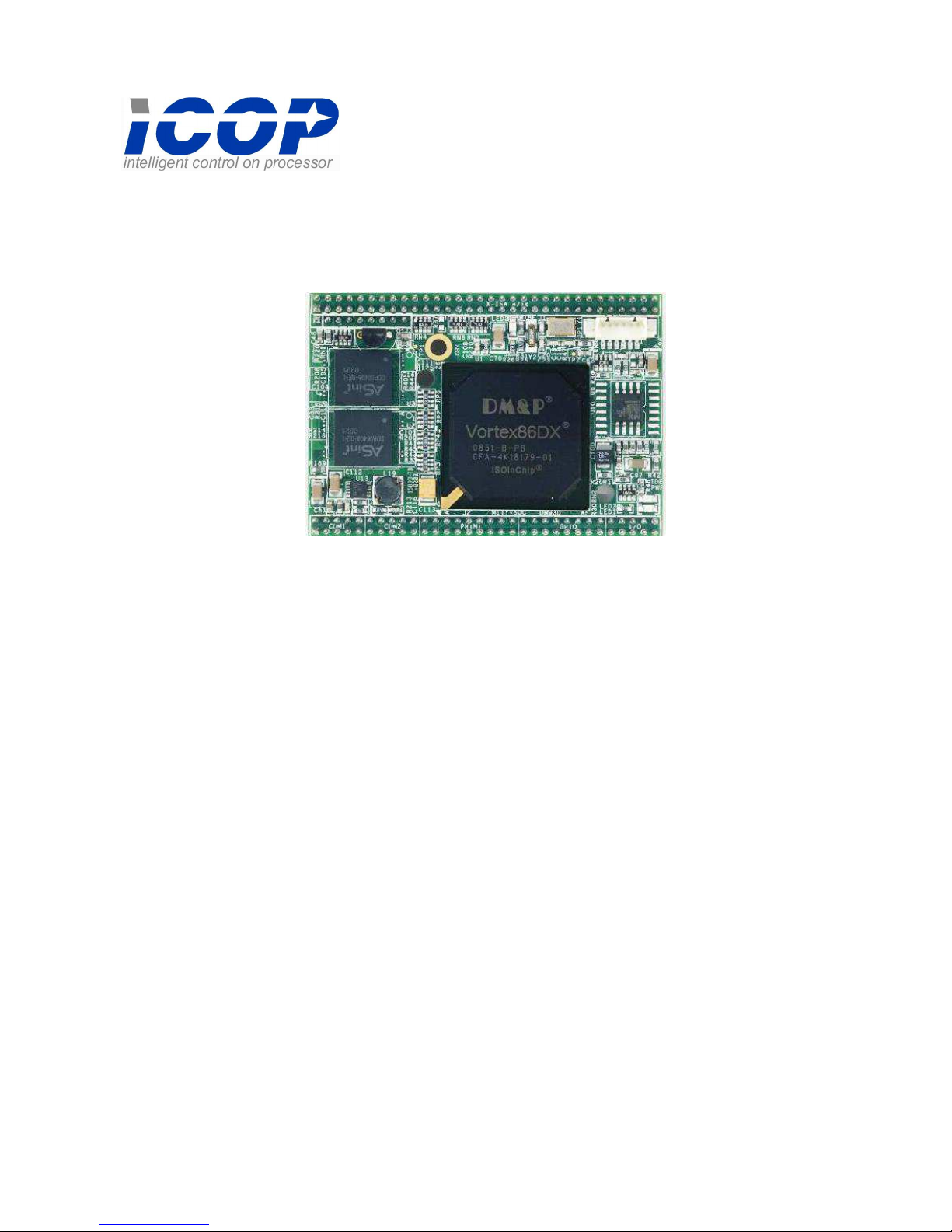
VDDX-6319RD-FB-D Vortex86DX Mity-SoC CPU Module
1
C h a p t e r 1
Introduction
1.1 Packing List
Product Name Package
VSX-6119-1
Vortex86SX/ DX CPU Mity-SoC Development
board x1
Manual & Drivers CD x 1
RS232 cable x 3
PRINTER cable x1
IDE cable x 1
USB cable x 1
(U SB port x 2
)
GPIO cable x 1
YKB for PS/2 Keyboard & Mouse x 1
Product Name Package
VDX-6319RD-FB-D
(Onboard EmbedDiSk
512MB)
Embedded Vortex86DX Mity-SoC CPU Module x1
Product Name Package
ICOP-6019-VGA
Mity-So C VGA/LCD development Kit x1

VDDX-6319RD-FB-D Vortex86DX Mity-SoC CPU Module
2
1.2 Product Description
The VDX-6319RD-FB-D family of low-power x86 embedded controller is designed to meet
Mity-SoC specification, and integrated with the following features.
800MHz Vortex86DX System-On-Chip
256MB DDR2 system memory
1 USB 2.0 (host)
Up to 2 serial ports
16-bit GPIO x1
x-ISA bus
2 watchdog timer
JTAG interface
AMI BIOS
Onboard EmbedDisk 512MB
4MB SPI flash
Single voltage +5V DC
Support extended operating
temperature range of -20°C to +70°C
The VDX-6319RD-FB-D Mity-SoC family of embedded controller is designed as the kernel of
your own application, to provide migration path for projects facing end-of-life challenges with
their existing x86 based Mity-Mite controller. The VDX-6319RD-FB-D family of controller is
designed as a plug in replacement, with backward compatibility to support legacy software to
help extend existing product life cycle without heavy re-engineering.
VDX-6319RD-FB-D is suitable for broad range of data-acquisition, Industrial automation,
Process control, Automotive controller, AVL, Intelligent Vehicle management devic,Medical
device, Human machine interface, Robotics, machinery control And more…application that
required small footprint, low-power and low-cost hardware with open industry standard such as
Mity-SoC.
VDX-6319RD-FB-D Vortex86DX Mity-SoC CPU Module
3
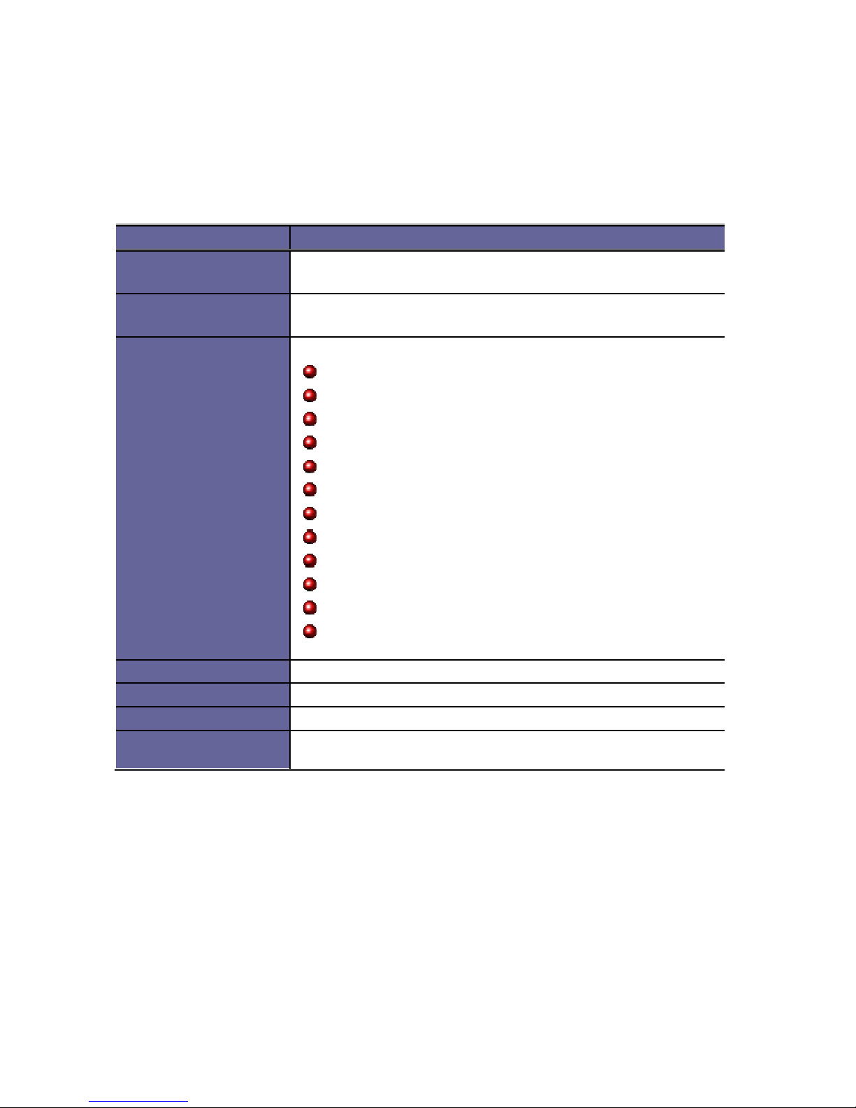
1.3 Specifications
VSX-6119-1 (Mity-SoC ISA bus Development board)
Features VSX-6119-1
Bus Interfac e
16-bit x-ISA interface
PC/104 standard compliant
Status indica tor
Digit Type 7-Segment LED Display for POST Code x2
GPIO LED x16
Connectors
2.54mm 26-pin box header for Printer x1
2.54mm 20-pin box header for 16-bit GPIO x1
2.54mm 10-pin box header for RS-232 x1
2.54mm 5-pin box header for Keyboard x1
2.54mm 10-pin box header for USB x1
2.54mm 2-pin header for Reset x1
External 15-pin D-Sub female connector for VGA
External 9-pin D-Sub male connector for RS-232 x1
External Mini DIN connector for Keyboard/Mouse x1
4-pin Molex connector for Power input x1
2-pin Terminal strip for Power input x1
DC Jack for Power input x1
Power Requirement
Single Voltage +5V
@
150mA
Dimension
185 x 122mm (7.28 x 4.8 inches)
Weight
172g
Operating
Temperature
-20oC ~ +70oC
-40°C ~ +85°C (Optional)
VDX-6319RD-FB-D Vortex86DX Mity-SoC CPU Module
4
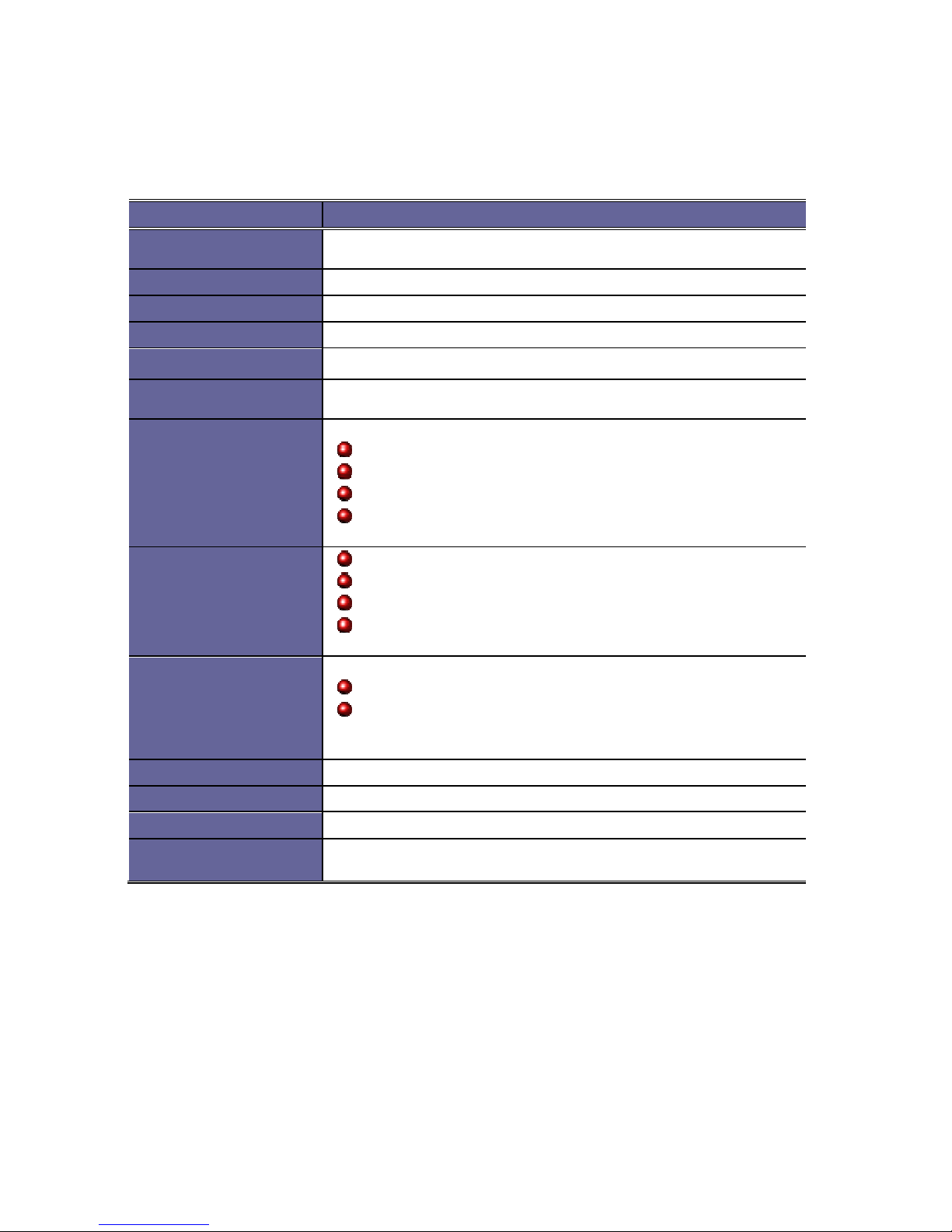
VDX-6319RD-FB-D
Features VDX-6319RD-FB-D
CPU
DM&P SoC CPU Vortex86DX- 800MHz
Real Time Clock with Lithium Battery Backup
Cache
L1:16K I-Cache, 16K D-Cache L2:128KB Cache
BIOS
AMI BIOS
Bus Interfac e
16-bit x-ISA interface
System Memory
256MB DDR2 onboard
Watchdog Timer
Software programmable from 30.5 us to 512 seconds x2
sets(Watchdog 1 fully compatible with M6117D)
I /O Interface
RS-232 port x2 (TTLx2)
USB port (ver2.0) x1
Parallel port x1
16-bit GPIO port x1
Connectors
2.00 mm ∅ 64-pin header for 16-bit x-ISA x1
2.00 mm ∅ 64-pin header for I/O interface x1
2.00 mm ∅ 9-pin header for DMA x1
1.25mm ∅ 6-pin Wafer for JTAG x1
Flash Disk Support
Onboard 4MB SPI Flash Disk (Driver: A)
Onboard EmbedDisk 512MB (Driver: C)
Power Requirement
Single Voltage +5V
@
400mA
Dimension
65mm X 45mm (2.56 x1.77 inches)
Weight
30g
Operating
Temperature
-20oC ~ +70oC
-40°C ~ +85°C (Optional)
VDX-6319RD-FB-D Vortex86DX Mity-SoC CPU Module
5
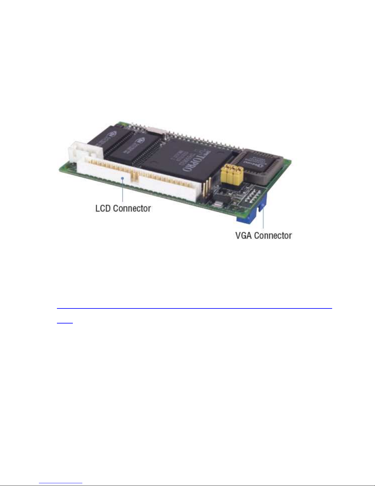
ICOP-6019-VGA
Features ICOP-6019-VGA
Chipset
TOPRO TP6508IQ
VGA and Mono/STN/DSTN/TFT Flat Panel interface
support
Bus
16-bit x-ISA interface
Video Memory
Onboard 1MB EDO RAM, support resolution up to
1024x768, 256 colors
Bus Interfac e
PC/104+ standard compliant
Connectors
2.0mm 44-pin box header for LCD x1
2.0mm 10-pin box header for VGA x1
2.54mm 4-pin wafer for +12V, -12V, -5V DC-in x1
Power Requirement
Single Voltage +5V@200mA
Dimension
80 x 50mm (3.14 x 1.96 inches)
Weight
32g
Operating
Temperature
-20oC ~ +60oC
VDX-6319RD-FB-D Vortex86DX Mity-SoC CPU Module
6
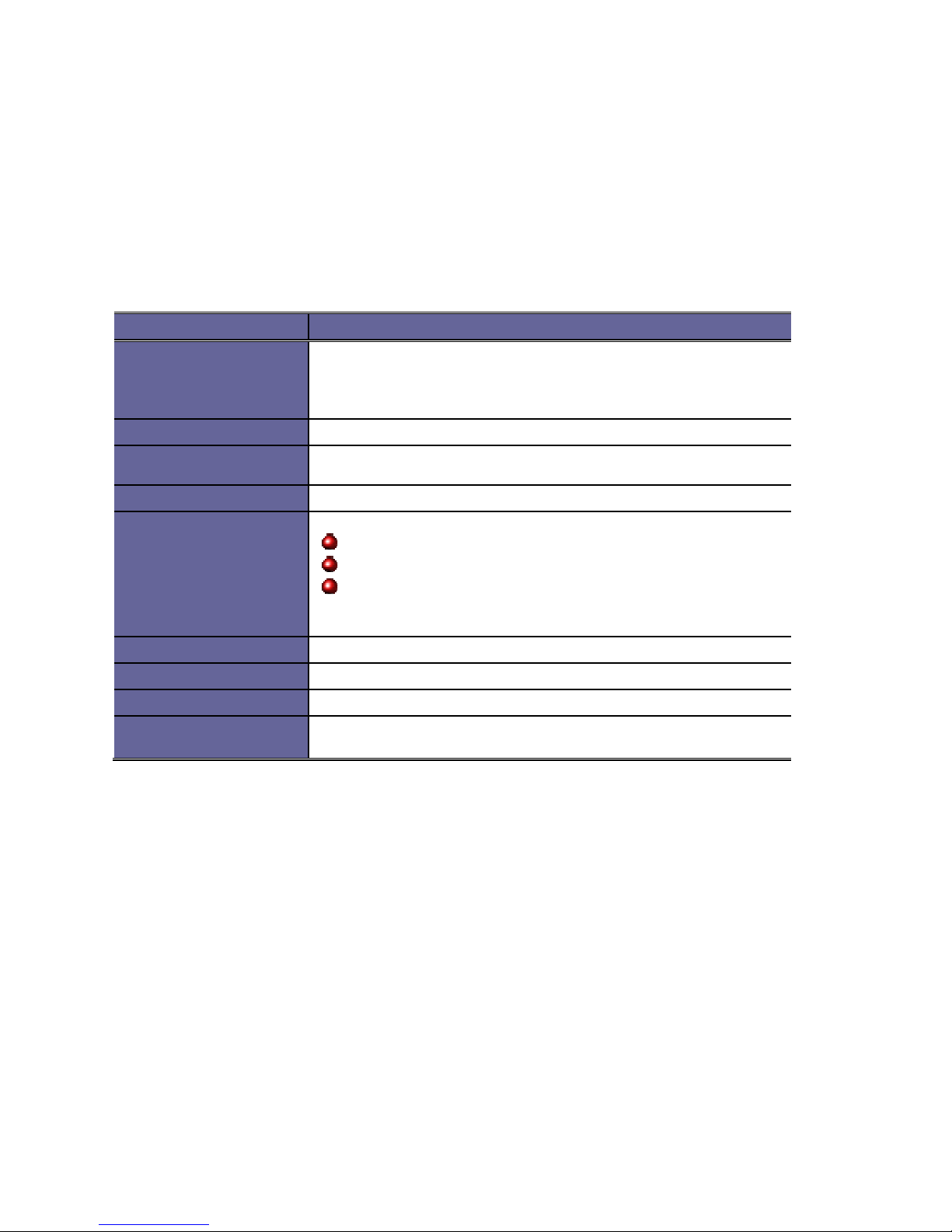
1.4 Order Selection

VDX-6319RD-FB-D Vortex86DX Mity-SoC CPU Module
7
1.5 Board Dimension
VDX-6319RD-FB-D
VDX-6319RD-FB-D Vortex86DX Mity-SoC CPU Module
8
C h a p t e r 2
Installation
2.1 Board Outline
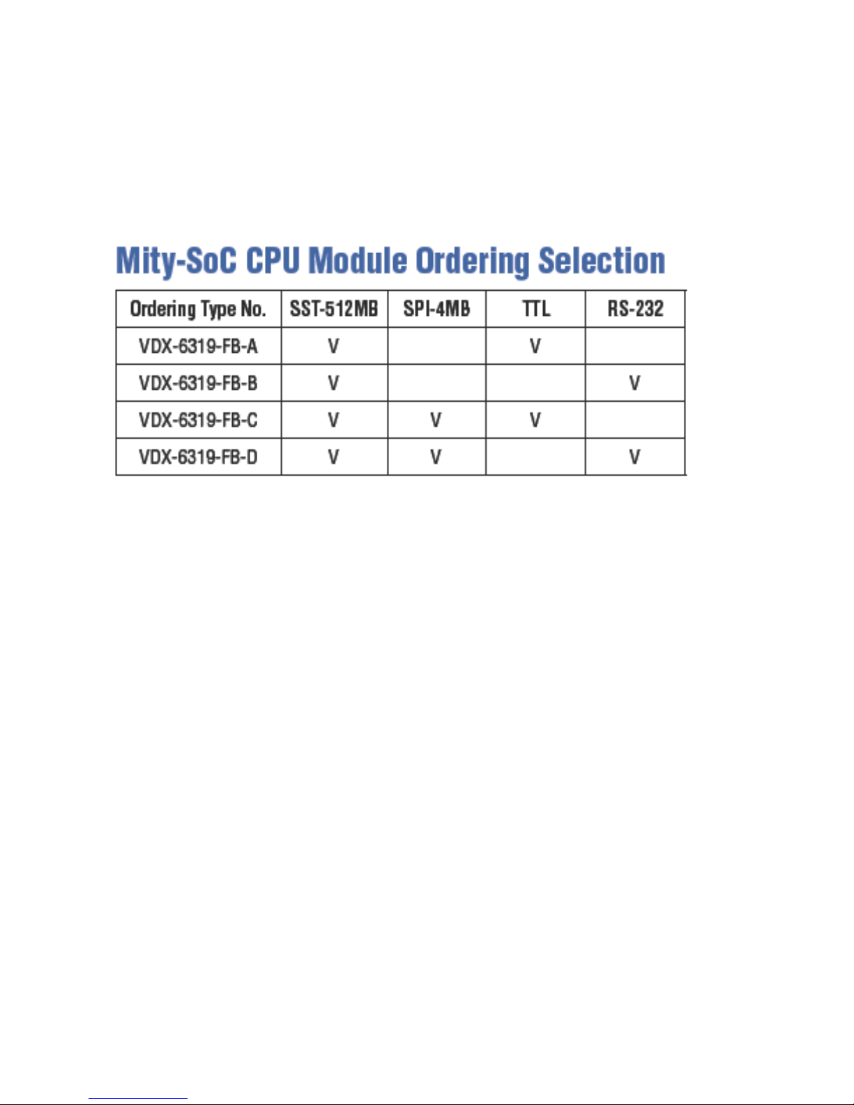
VSX-6119-1 (Mity-SoC ISA bus Development board)
VDX-6319RD-FB-D Vortex86DX Mity-SoC CPU Module
9
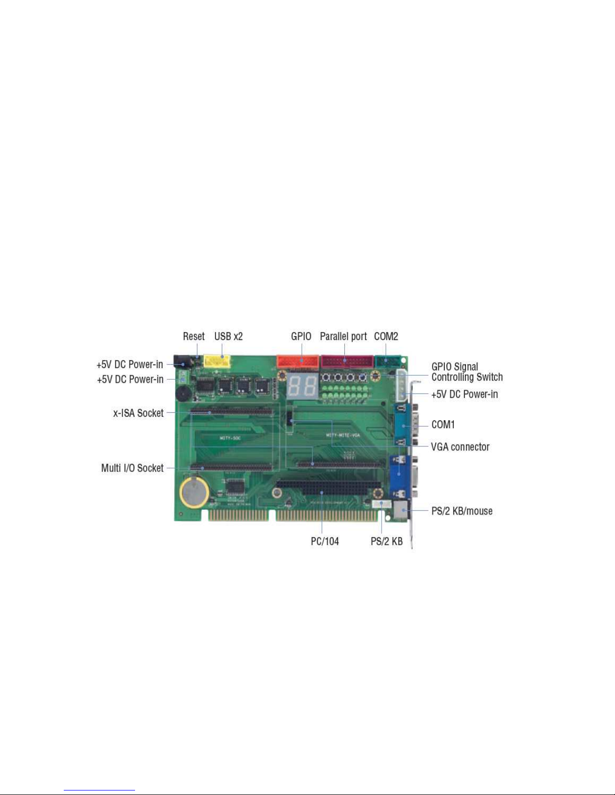
VDX-6319RD-FB-D
Note: VGA, ICOP-6019-VGA, function support via x-ISA Interface
VDX-6319RD-FB-D Vortex86DX Mity-SoC CPU Module
10
ICOP-6019-VGA
If you need more information about ICOP-6019-VGA, please visit our website at
http://www.icop.com.tw/en/product/Processor-Module-ICOP-6019-VGA/ICOP-6019-VGA
.html
VDX-6319RD-FB-D Vortex86DX Mity-SoC CPU Module
11
2.2 Connectors & Jumpers Location
Connectors
VDX-6319RD-FB-D Vortex86DX Mity-SoC CPU Module
12
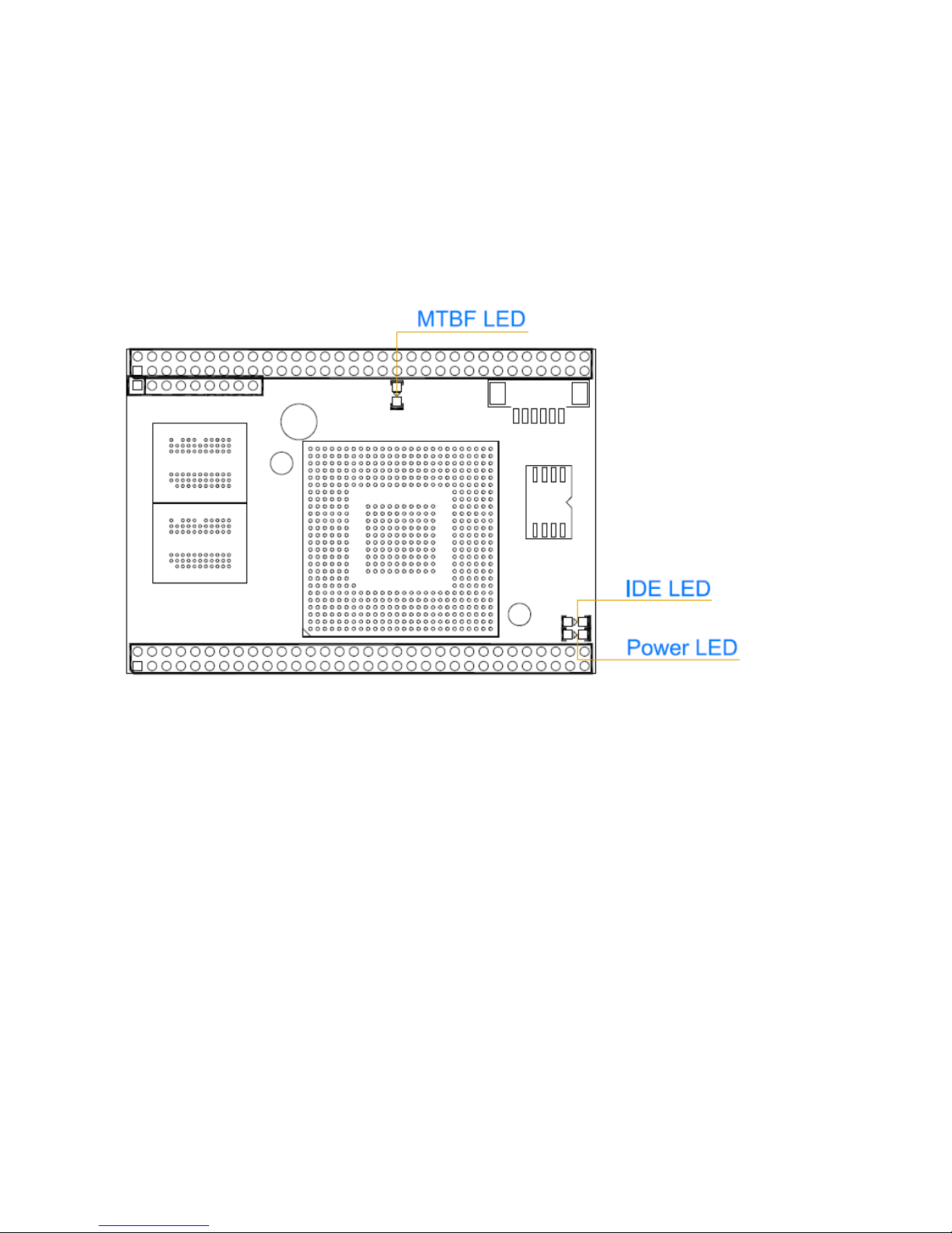
Jumpers & LEDs
VDX-6319RD-FB-D Vortex86DX Mity-SoC CPU Module
13
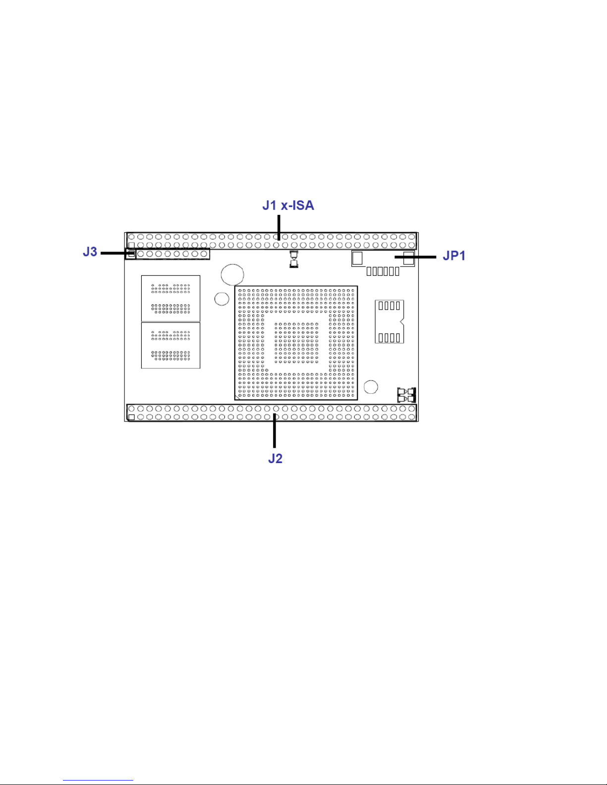
2.3 Connectors & Jumpers Summary
VSX-6119-1 (Mity-SoC ISA bus Development board)
Summary Table
Nbr Description Type of Connections Pin nbrs.
J1 x-ISA Connector – 64 pin Box Header, 2.0∅, 32x2 64-pin
J2 ISA bus Connector, SL62 62-pin Gold finger 62-pin
J3 ISA bus Connector, SL36 36-pin Gold finger 36-pin
J4 PC104 Connector – 64 pin Box Header, 2.54∅ ,32x2
64-pin
J5 PC104 Connector – 40 pin Box Header, 2.54∅ ,20x2
40-pin
J6 Mity-Mite VGA Connector Box Header, 2.0∅, 32x2 64-pin
J7 USB Pin Header, 2,54∅,5x2 10-pin
J8 Multi I/O Connector – 64 pin
Box Header, 2.0∅, 32x2 64-pin
J9 GPIO Port Box Header, 2.54∅ ,10x2
20-pin
J10 COM1 D-Sub Connector 9-pin
J11 COM2 Box Header, 2.54∅, 5x2 10-pin
J12 Reset Pin Header, 2.54∅, 1x2 2-pin
J13 PS/2 Keyboard Box Header,2.54∅, 1x5 5-pin
J14 VGA D-Sub female connector 15-pin
J15 Power Connector Terminal Block 5.0∅ , 2x1
2-pin
J16 Power Connector DC -JACK 3-pin
J17
Power Connector Box Header, 5.0∅ Molex
4-pin
J18 VGA connector Box Header, 2.54∅ , 5x2
10-pin
J19 PS/2 Keyboard Mini-Din Connector 9-pin
J20 PRINT Box Header, 2.54∅ ,13x2
26-pin
S1~S4 Switch Input
U5 80 PORT (7Segment Display)
18-pin DIP SSD 18-pin
SP1 BUZZER
GP0~GP15 LED Display
 Loading...