

Page 1

DUAL BAND TRANSCEIVER
S-15120XZ-C1
March 2015
Page 2

INTRODUCTION CAUTION
This service manual describes the latest technical informa-
tion for the IC-2730A and IC-2730E
DUAL BAND TRANSCEIVER, at
the time of publication.
MODEL VERSION
TPE-01 #04 25 W/15 W/5 W
IC-2730A
IC-2730E
USA-01 #05
KOR-01 #06
EXP-01 #09
EUR-01 #02
ITR-01 #03
CHN-01 #10
VERSION
NUMBER
TX POWER
50 W/15 W/5 W
NEVER connect the transceiver to an AC outlet or to a DC
power supply that uses more than the specifi ed voltage. This
will ruin the transceiver.
DO NOT expose the transceiver to rain, snow or liquids.
DO NOT reverse the polarities of the power supply when con-
necting the transceiver.
DO NOT apply an RF signal of more than 20 dBm (100 mW)
to the antenna connector. This could damage the transceiv-
er’s front-end.
To upgrade quality, any electrical or mechanical parts
and internal circuits are subject to change without notice
or obligation.
(IC-2730A)
ORDERING PARTS
Be sure to include the following four points when ordering
replacement parts:
1. 10-digit Icom part number
2. Component name
3. Equipment model name and unit name
4. Quantity required
1. Make sure that the problem is internal before dis-assem-
bling the transceiver.
2. DO NOT open the transceiver until the transceiver is dis-
connected from its power source.
3. DO NOT force any of the variable components. Turn them
slowly and smoothly.
4. DO NOT short any circuits or electronic parts. An insulated
REPAIR NOTES
tuning tool MUST be used for all adjustments.
<ORDER EXAMPLE>
1110003491 S.IC TA31136FNG IC-2730A MAIN UNIT 5 pieces
8820001210 Screw 2438 screw IC-2730E Top cover 10 pieces
5. DO NOT keep power ON for a long time when the trans-
ceiver is defective.
6. DO NOT transmit power into a Standard Signal Generator
or a Sweep Generator, otherwise the RF power may dam-
Addresses are provided on the inside back cover for your
convenience.
age them.
7. ALWAYS connect a 50 dB to 60 dB attenuator between the
transceiver and a Deviation Meter or Spectrum Analyzer,
when using such test equipment.
8. READ the instructions of the test equipment thoroughly
before connecting it to the transceiver.
Icom, Icom Inc. and the Icom logo are registered trademarks of Icom Incorporated (Japan) in Japan, the United States, the
United Kingdom, Germany, France, Spain, Russia, Australia, New Zealand, and/or other countries.
Page 3

TABLE OF CONTENTS
SECTION 1 SPECIFICATIONS
SECTION 2 INSIDE VIEWS
SECTION 3 DISASSEMBLY INSTRUCTION
SECTION 4 CIRCUIT DESCRIPITON
4-1 RECEIVER CIRCUITS ...................................................................................... 4-1
4-2 TRANSMIT CIRCUITS ...................................................................................... 4-5
4-3 FREQUENCY SYNTHESIZER CIRCUITS ....................................................... 4-7
4-4 VOLTAGE BLOCK DIAGRAM ........................................................................... 4-8
SECTION 5 ADJUSTMENT PROCEDURES
5-1 PREPARATION ................................................................................................. 5-1
5-2 FREQUENCY ADJUSTMENT .......................................................................... 5-3
5-3 TRANSMIT ADJUSTMENT ............................................................................... 5-3
5-4 RECEIVE ADJUSTMENT ................................................................................. 5-5
SECTION 6 PARTS LIST
SECTION 7 MECHANICAL PARTS
SECTION 8 BOARD LAYOUTS
SECTION 9 BLOCK DIAGRAM
SECTION 10 VOLTAGE DIAGRAM
Page 4
SECTION 1. SPECIFICATIONS
DGeneral
• Frequency coverage:
EUR
ITR
TPE RX, TX 144–146 MHz, 430–432 MHz
USA
KOR RX, TX 144–146 MHz, 430–440 MHz
EXP,
CHN
*1 Guaranteed only 144–146 MHz *2 Guaranteed only 430–440 MHz *3 Not guaranteed *4 Guaranteed only 144–148 MHz *5 Guaranteed only 430–450 MHz
RX 118–174 MHz*
TX 144–146 MHz, 430–440 MHz
RX 118–136.99166 MHz*
TX 144–146 MHz, 430–434 MHz, 435–438 MHz
RX 118–174 MHz*
TX 144–148 MHz, 430–450 MHz*
RX 118–174 MHz*
TX 137–174 MHz*4, 400–470 MHz*
• Mode: F2D/F3E (FM/FM-N),
• Number of memory channels: 1000 channels
• Number of program scan channels: 25 channels
• Number of call channels: 2 channels
• Scan types: Full, Band, Program, Priority, Memory channel, Bank, Skip and Tone scans
• Antenna connector: SO-239
• Antenna impedance: 50 ø
• Usable temperature range: –10˚C to +60˚C, +14˚F to +140˚F
• Frequency stability: ±2.5 ppm (−10˚C to +60˚C, +14˚F to +140˚F)
• Frequency resolution: 5 kHz, 6.25 kHz, 8.33 kHz, 10 kHz, 12.5 kHz, 15 kHz, 20 kHz, 25 kHz, 30 kHz, 50 kHz
The 8.33 kHz step is not selectable, depending on the operating band or mode.
• Power supply: 13.8 V DC ±15% (negative ground)
• Current drain:
Transmit
Maximum current drain: 10.5 A at 25 W (TPE version)
Receive
Standby: 1.2 A
Maximum audio: 1.8 A
• Dimensions (projections not included):
Main unit: 150(W) 40(H) 151(D) mm, 5.9(W) 1.6(H) 5.9(D) inches
Controller:
• Weight (approximately):
Main unit: 1.2 kg, 2.6 lb
Controller: 140 g, 4.9 oz
1
, 375–550 MHz*
3
, 144–146 MHz, 430–434 MHz, 435–438 MHz
4
, 375–550 MHz*
4
, 375–550 MHz*
2
5
5
2
2
A3E (AM/AM-N) RX only
(2 edge frequencies in each channel)
150(W) 50(H) 27.2(D) mm,
13.0 A at 50 W (Other versions)
5.9(W) 2(H) 1.1(D) inches
D
Transmitter
• Modulation system: Variable reactance frequency modulation
• Type of emission: F2D, F3E
• Maximum deviation:
FM: ±5.0 kHz
FM-N: ±2.5 kHz
• Input impedance (Mic): 600 ø
• Spurious emission: –60 dBc
• Output power: High 25 W, Mid 15 W, Low 5 W (TPE version)
High 50 W, Mid 15 W, Low 5 W (Other versions)
1-1
Page 5
D
Receiver
• Receive system: Double superheterodyne system
• IF frequencies:
Left band 1st IF 38.85 MHz
2nd IF 450 kHz
Right band 1st IF 46.35 MHz
2nd IF 450 kHz
• Sensitivity (except spurious points):
Amateur bands
FM/FM-N (12 dB SINAD)
0.18 µV
Except Amateur bands
FM/FM-N (12 dB SINAD)
0.32 µV (137.000–159.995 MHz)
0.56 µV (160.000–174.000 MHz)
0.56 µV (375.000–399.995 MHz)
0.32 µV (400.000–499.995 MHz)
0.56 µV (500.000–550.000 MHz)
AM (10 dB S/N)
1 µV (118.000–136.99166 MHz)
• Squelch sensitivity: 0.13 µV (Threshold)
• Selectivity:
FM 60 dB
FM-N 55 dB
• Spurious and image rejection ratio:
60 dB
55 dB (Left band UHF)
• AF output power: 2.0 W (at 10% distortion into an 8 ø load)
• Output impedance (Speaker): 8 ø
1-2
Page 6

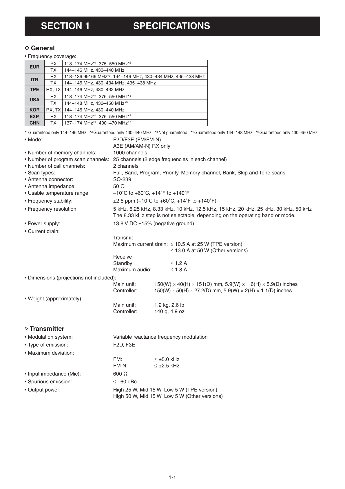
SECTION 2. INSIDE VIEWS
• CONTROL UNIT
+3.3 V REGULATOR
(IC6)
CPU
(IC1)
LCD DRIVER
(IC2)
RESET IC
(IC5)
+3.3 V REGULATOR
(IC7)
CLONING DATA LINE BUFFER
(IC102)
2-1
Page 7
CLONING DATA LINE BUFFER
(IC312)
AND LOGIC GATE IC
(IC108)
AF SW
(IC109)
ELECTRONIC VOLUME IC
(IC110)
+3.3 V REGULATOR
(IC314)
+5 V REGULATOR
(IC319)
AF LINE MUTE SW
(IC111)
D/A CONVERTER
(IC1)
1ST IF FILTER (Right band)
(FI105)
• MAIN UNIT
(TOP VIEW)
RESET IC
(IC308)
EEPROM
(IC301)
NOISE AMP (Left band)
(IC123)
NOISE AMP (Right band)
(IC122)
MIC MUTE SW/MIC GAIN SW
(IC100)
VOX AMP/IDC AMP/AF LPF
(IC112)
AF LPF/AF BUFFER
(IC103)
D/A CONVERTER
(IC102)
MODULATION MUTE SW
(IC205)
IF IC (Left band)
(IC121)
EXPANDER
(IC316)
EXPANDER
(IC315)
EXPANDER
(IC317)
MIC AMP
(IC101)
IF IC (Right band)
(IC120)
1ST IF FILTER (Right band)
(FI104)
2-2
Page 8

• MAIN UNIT
(BOTTOM VIEW)
DISCRIMINATOR (Right band)
(X101)
2ND IF FILTER (Right band)
(FI101)
2ND IF FILTER (Right band)
(FI100)
TX POWER AMP (UHF band)
(IC4)
TX POWER AMP
(VHF band)
(IC3)
+3.3 V REGULATOR
(IC311)
CURRENT DETECTOR IC
(IC310)
+8 V REGULATOR
(IC321)
+8 V REGULATOR
(IC325)
+8 V REGULATOR
(IC313)
PLL IC (Right band)
(IC206)
REFERENCE FREQUENCY
OSCILLATOR (Right band)
(X201)
DISCRIMINATOR (Left band)
(X102)
2ND IF FILTER (Left band)
(FI103)
2ND IF FILTER (Left band)
(FI102)
PLL IC (Left band)
(IC201)
REFERENCE FREQUENCY
OSCILLATOR (Left band)
(X200)
AF LINE SW
(IC119)
AF MUTE SW
(IC104)
CPU
(IC300)
+3.3 V REGULATOR
(IC306)
AF POWER AMP
(IC105)
AF POWER AMP
(IC106)
VOLTAGE DETECTOR IC
(IC324)
VOLTAGE DETECTOR IC
(IC320)
CLOCK OSCILLATOR
(X300)
2-3
Page 9

SECTION 3. DISASSEMBLY INSTRUCTION
1. Removing the CONTROL UNIT
1) Remove all knobs from the controller.
Controller
2) Remove four screws from the rear panel.
3) Separate the rear panel from the front panel as-
sembly.
Front panel assembly
Rear panel
4) Remove the CONTROL UNIT from the front panel.
Front panel
2. Removing the MAIN UNIT
1) Remove eight screws from the top cover.
2) Remove the top cover from the chassis.
Top cover
Screws ×8
CHASSIS
3) Disconnect the speaker cable from the MAIN UNIT.
4) Remove the clip from the chassis.
Speaker
SPEAKER
CABLE
CONTROL UNIT
Clip
CHASSIS
5) Remove seven screws from the bottom cover.
Bottom cover
Screws×7
3-1
CHASSIS
(Continued on the next page.)
Page 10

6) Unsolder three points at the antenna connector.
7) Disconnect the cooling fan cable.
UNSOLDER
Solder
remover
COOLING FAN
CABLE
8) Remove total of 17 screws from the MAIN UNIT.
Screws ×17
9) Remove the MAIN UNIT from the chassis.
MAIN UNIT
CHASSIS
3-2
Page 11
SECTION 4. CIRCUIT DESCRIPTION
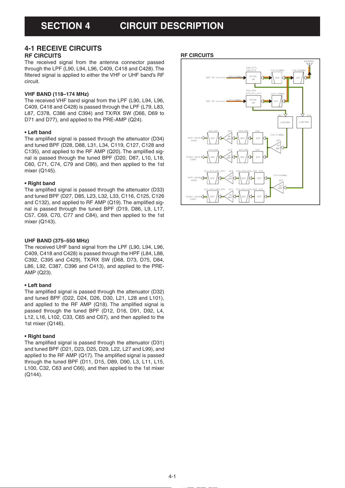
4-1 RECEIVE CIRCUITS
RF CIRCUITS
The received signal from the antenna connector passed
through the LPF (L90, L94, L96, C409, C418 and C428). The
fi ltered signal is applied to either the VHF or UHF band’s RF
circuit.
VHF BAND (118–174 MHz)
The received VHF band signal from the LPF (L90, L94, L96,
C409, C418 and C428) is passed through the LPF (L79, L83,
L87, C378, C386 and C394) and TX/RX SW (D66, D69 to
D71 and D77), and applied to the PRE-AMP (Q24).
• Left band
The amplifi ed signal is passed through the attenuator (D34)
and tuned BPF (D28, D88, L31, L34, C119, C127, C128 and
C135), and applied to the RF AMP (Q20). The amplifi ed sig-
nal is passed through the tuned BPF (D20, D87, L10, L18,
C60, C71, C74, C79 and C86), and then applied to the 1st
mixer (Q145).
• Right band
The amplifi ed signal is passed through the attenuator (D33)
and tuned BPF (D27, D85, L23, L32, L33, C116, C125, C126
and C132), and applied to RF AMP (Q19). The amplifi ed sig-
nal is passed through the tuned BPF (D19, D86, L9, L17,
C57, C69, C70, C77 and C84), and then applied to the 1st
mixer (Q143).
RF CIRCUITS
UHF TX circuit
VHF TX circuit
Left band
(VHF)
Right band
(VHF)
Left band
(UHF)
Right band
(UHF)
BPF
BPF
BPF
BPF
400-470MHz
137-174MHz
RF
AMP
RF
AMP
RF
AMP
RF
AMP
BPF
BPF
BPF
BPF
D68,D73,
D84,D75
TX/RX
SW
D66,D69
D70,D71,D77
TX/RX
SW
D34D28,D88Q20D20,D87
ATT
D33D27,D85Q19D19,D86
ATT
ANTENNA
HPF
AMP
Q24
RF
LIMITER
Q23
RF
AMP
118-550MHz
LPF
D79D81
LIMITER
375-550MHz
118-174MHz
LPF
118-174MHz
D32D22,D24,D26,D30Q18D12,D16,D91,D92
375-550MHz
ATT
D31D21,D23,D25,D29Q17D11,D15,D89,D90
ATT
UHF BAND (375–550 MHz)
The received UHF band signal from the LPF (L90, L94, L96,
C409, C418 and C428) is passed through the HPF (L84, L88,
C392, C395 and C429), TX/RX SW (D68, D73, D75, D84,
L86, L92, C387, C396 and C413), and applied to the PRE-
AMP (Q23).
• Left band
The amplifi ed signal is passed through the attenuator (D32)
and tuned BPF (D22, D24, D26, D30, L21, L28 and L101),
and applied to the RF AMP (Q18). The amplifi ed signal is
passed through the tuned BPF (D12, D16, D91, D92, L4,
L12, L16, L102, C33, C65 and C67), and then applied to the
1st mixer (Q146).
• Right band
The amplifi ed signal is passed through the attenuator (D31)
and tuned BPF (D21, D23, D25, D29, L22, L27 and L99), and
applied to the RF AMP (Q17). The amplifi ed signal is passed
through the tuned BPF (D11, D15, D89, D90, L3, L11, L15,
L100, C32, C63 and C66), and then applied to the 1st mixer
(Q144).
4-1
Page 12

1ST IF CIRCUITS
VHF BAND
• Left band
The received signal from the RF circuit and 1st LO signal are
applied to the 1st IF mixer (Q145) and mixed, resulting in the
38.85 MHz 1st IF signal.
The 1st IF signal is applied to the 1st IF fi lter (FI105), through
the band SW (D121).
2ND IF CIRCUITS
• Left band
IC121 is an IF IC, which contains the 2nd mixer, limiter AMP,
noise AMP, quadrature detector, AM detector, AGC controller,
signal strength detector, and so on.
The 1st IF signal from the 1st IF AMP (Q138) and 38.4 MHz
2nd LO signal are mixed, resulting in the 450 kHz 2nd IF sig-
nal.
• Right band
The received signal from the RF circuit and 1st LO signal are
applied to the 1st IF mixer (Q143) and mixed, resulting in the
46.35 MHz 1st IF signal.
The 1st IF signal is applied to the 1st IF fi lter (FI104), through
the band SW (D119).
UHF BAND
• Left band
The received signal from the RF circuit and 1st LO signal are
applied to the 1st IF mixer (Q146) and mixed, resulting in the
38.85 MHz 1st IF signal.
The 1st IF fi lter is applied to the 1st IF fi lter (FI105), through
the band SW (D122).
• Right band
The received signal from the RF circuit and 1st LO signal are
applied to the 1st IF mixer (Q144) and mixed, resulting in the
46.35 MHz 1st IF signal.
The 1st IF signal is applied to the 1st IF fi lter (FI104), through
the band SW (D120).
The 2nd IF signal is output from pin 3, and passed through
the ceramic fi lter (FI102: For FM-N or FI103: For FM), and
then applied to IC121 from pins 5 and 7.
• Right band
IC120 is an IF IC, which contains the 2nd mixer, limiter AMP,
noise AMP, quadrature detector, AM detector, AGC controller,
signal strength detector, and so on.
The 1st IF signal from the 1st IF AMP (Q137) and 45.9 MHz
2nd LO signal are mixed, resulting in the 450 kHz 2nd IF sig-
nal.
The 2nd IF signal is output from pin 3, and passed through
the ceramic fi lter (FI100: For FM-N or FI101: For FM), and
then applied to IC120 from pins 5 and 7.
FM DEMODULATION CIRCUITS
• Left band
The 2nd IF signal applied pin 7 is amplifi ed by the limiter AMP,
and then demodulated by the quadrature detector with the
ceramic resonator (X102).
The demodulated AF signal is output from pin 11, and then ap-
plied to the AF circuit, through the AF SW (IC119, pins 8, 9).
The fi ltered signal is amplifi ed by the IF AMP (Q137), and ap-
plied to the IF IC (IC120, pin 20).
1ST IF CIRCUITS
Left band 1st LO (VHF)
Left band VHF RF circuit
Q145
Right band 1st LO (UHF)
Right band VHF RF circuit
Q143
Left band 1st LO (UHF)
Left band UHF RF circuit
Q146
Right band 1st LO (UHF)
Right band UHF RF circuit
Q144
Left band
2nd IF circuit
Right band
2nd IF circuit
FI105
Q138
IF
XTAL
AMP
BPF
38.85MHz
Left band 1st IF circuit
Q137
FI104
IF
XTAL
AMP
BPF
46.35MHz
Right band 1st IF circuit
D121,D122
RX
SW
D119,D120
RX
SW
• Right band
The 2nd IF signal applied pin 7 is amplifi ed by the limiter AMP,
and then demodulated by the quadrature detector with the
ceramic resonator (X101).
The demodulated AF signal is output from pin 11, and then ap-
plied to the AF circuit, through the AF SW (IC119, pins 1, 2).
4-2
Page 13

AM DETECTOR CIRCUITS
• Left band
The 2nd IF signal applied from pin 5 is amplifi ed by the IF
AMP, and then demodulated by the amplitude detector in the
IF IC (IC121).
The demodulated AF signal is output from pin 14, and
then applied to the AF circuits, through the AF SW (IC119,
pins 11, 10).
2ND IF AND DEMODULATOR CIRCUITS (Left band)
X200
Q200
38.4MHz
X3
Left band
AF circuit
IC119
DET OUT
SELECT
AM
FM
D107,D108,D111,D112
12.8MHz
IF IC
WIDE/NARROW
X102
IC121
Left band
1st IF circuit
In the AM mode, the AGC circuit in the IF IC automatically
adjusts the gain of RF AMPs (Q18 and Q20) and 1st IF AMP
(Q138), to keep the signal level constant.
The demodulated AF signal is applied to the RX AF circuit.
• Right band
The 2nd IF signal applied from pin 5 is amplifi ed by the IF
AMP, and then demodulated by the amplitude detector in the
IF IC (IC120).
The demodulated AF signal is output from pin 14, and then
applied to the AF circuits, through the AF SW (IC119, pins
4, 3).
In the AM mode, the AGC circuit in the IF IC automatically
adjusts the gain of RF AMPs (Q17 and Q19) and 1st IF AMP
(Q137), to keep the signal level constant.
The demodulated AF signal is applied to the RX AF circuit.
CERAMIC
CERAMIC
BPF
FI102 FI103
BPF
LIF
2ND IF AND DEMODULATOR CIRCUITS (Right band)
X201
Q220
45.9MHz
X3
Right band
AF circuit
DET OUT
SELECT
AM
FM
CERAMIC
FI100 FI101
IF IC
WIDE/NARROW
D105,D106,D109,D110
CERAMIC
BPF
BPF
15.3MHz
X101
IC120IC119
Right band
1st IF circuit
RIF
4-3
Page 14

RX AF CIRCUITS
• Left band
The demodulated AF signal from the AF SW (IC119) is
passed through the AF mute SW (IC111, pins 4, 3) and AF fi l-
ter (Q113), and then applied to the volume IC (IC110, pin 4),
which adjusts the AF signal in level.
The level-adjusted AF signal from the volume IC (IC110,
pin 11) is passed through the AF SW (IC109, pins 2, 1), which
selects the AF signal from Left and Right bands.
When output from [EXTERNAL SPEAKER JACK1]
The output signal from the AF SW (IC109) is passed through
the AF MUTE SW (Q104 and Q105), and applied to the AF
AMP (IC105, pin 1).
The amplifi ed AF signal is applied to the internal speaker
(CHASSIS: SP1) or an external speaker, through [EXTER-
NAL SPEAKER JACK1] (J101).
• Right band
The demodulated AF signal from the AF SW (IC119) is
passed through the AF mute SW (IC111, pins 8, 9) and AF
fi lter (Q112), and then applied to the volume IC (IC110, pin 3),
which adjusts the AF signal in level.
The level-adjusted AF signal from the volume IC (IC110,
pin 12) is passed through the AF SW (IC109, pins 3, 4), which
selects the AF signal from Left and Right bands.
• RX AF CIRCUITS
J101
SP1
J102
IC105 Q104 Q105
AF
SP
AMP
MUTE
IC106
AF
AMP
Optional module
Q106
MUTE
BTAF
MUTE
SP
SP
IC109
AFSW
IC107
BUFF
When output from [EXTERNAL SPEAKER JACK2]
The output signal from the AF SW (IC109) is passed through
the AF MUTE SW (Q106), and applied to the AF AMP (IC106,
pin 1).
The amplifi ed AF signal is applied to [EXTERNAL SPEAKER
JACK2] (J102).
TX AF circuit
IC110 IC111
ELEC.
IC103
AF
FIL
Q113,Q140
AF
FIL
Modulation circuit
IC103
BUFF
IC103
BUFF
DETMUTE
L_RMUTE R_RMUTE
2nd IF circuit (Left band )
2nd IF circuit (Right band )
LPF
RPT
IC104
RPT
SW
Q112,Q139
VR
4-4
Page 15
4-2 TRANSMIT CIRCUITS
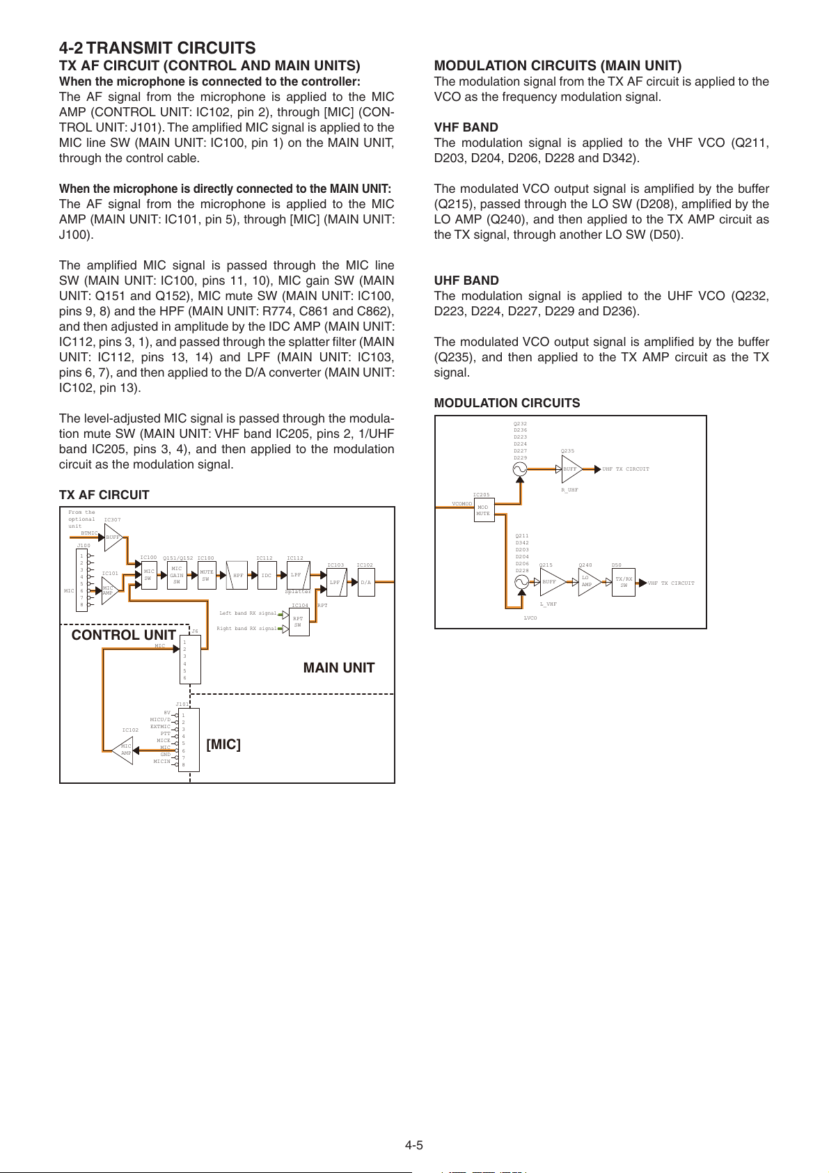
TX AF CIRCUIT (CONTROL AND MAIN UNITS)
When the microphone is connected to the controller:
The AF signal from the microphone is applied to the MIC
AMP (CONTROL UNIT: IC102, pin 2), through [MIC] (CON-
TROL UNIT: J101). The amplifi ed MIC signal is applied to the
MIC line SW (MAIN UNIT: IC100, pin 1) on the MAIN UNIT,
through the control cable.
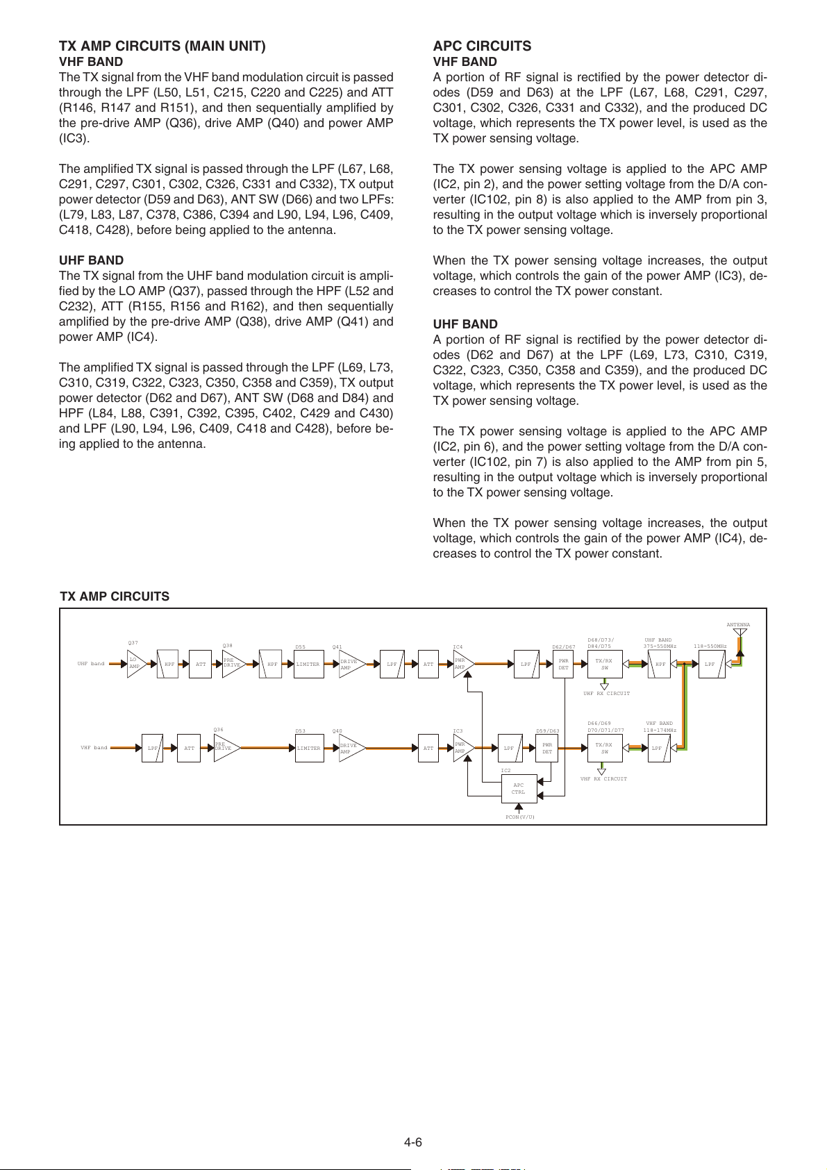
MODULATION CIRCUITS (MAIN UNIT)
The modulation signal from the TX AF circuit is applied to the
VCO as the frequency modulation signal.
VHF BAND
The modulation signal is applied to the VHF VCO (Q211,
D203, D204, D206, D228 and D342).
When the microphone is directly connected to the MAIN UNIT:
The AF signal from the microphone is applied to the MIC
AMP (MAIN UNIT: IC101, pin 5), through [MIC] (MAIN UNIT:
J100).
The amplifi ed MIC signal is passed through the MIC line
SW (MAIN UNIT: IC100, pins 11, 10), MIC gain SW (MAIN
UNIT: Q151 and Q152), MIC mute SW (MAIN UNIT: IC100,
pins 9, 8) and the HPF (MAIN UNIT: R774, C861 and C862),
and then adjusted in amplitude by the IDC AMP (MAIN UNIT:
IC112, pins 3, 1), and passed through the splatter fi lter (MAIN
UNIT: IC112, pins 13, 14) and LPF (MAIN UNIT: IC103,
pins 6, 7), and then applied to the D/A converter (MAIN UNIT:
IC102, pin 13).
The level-adjusted MIC signal is passed through the modula-
tion mute SW (MAIN UNIT: VHF band IC205, pins 2, 1/UHF
band IC205, pins 3, 4), and then applied to the modulation
circuit as the modulation signal.
TX AF CIRCUIT
From the
optional
IC307
unit
BTMIC
BUFF
J100
1
2
3
4
5
6
MIC
7
8
CONTROL UNIT
IC101
MIC
AMP
IC100
MIC
SW
Q151/Q152
MIC
MIC
GAIN
MUTE
SW
SW
J6
1
2
3
4
5
6
IC112IC100 IC112
HPF
IDC
Left band RX signal
Right band RX signal
Splatter
IC103 IC102
LPF
LPF
IC104
RPT
RPT
SW
MAIN UNIT
D/A
The modulated VCO output signal is amplifi ed by the buffer
(Q215), passed through the LO SW (D208), amplifi ed by the
LO AMP (Q240), and then applied to the TX AMP circuit as
the TX signal, through another LO SW (D50).
UHF BAND
The modulation signal is applied to the UHF VCO (Q232,
D223, D224, D227, D229 and D236).
The modulated VCO output signal is amplifi ed by the buffer
(Q235), and then applied to the TX AMP circuit as the TX
signal.
MODULATION CIRCUITS
Q232
D236
D223
VCOMOD
IC205
MOD
MUTE
D224
D227
D229
Q211
D342
D203
D204
D206
D228
LVCO
Q215
BUFF
L_VHF
Q235
BUFF
R_UHF
Q240
LO
AMP
UHF TX CIRCUIT
D50
TX/RX
SW
VHF TX CIRCUIT
IC102
MIC
AMP
MICU/D
EXTMIC
MICE
MICIN
J101
8V
1
2
3
PTT
4
5
MIC
GND
[MIC]
6
7
8
4-5
Page 16
TX AMP CIRCUITS (MAIN UNIT)
VHF BAND
The TX signal from the VHF band modulation circuit is passed
through the LPF (L50, L51, C215, C220 and C225) and ATT
(R146, R147 and R151), and then sequentially amplifi ed by
the pre-drive AMP (Q36), drive AMP (Q40) and power AMP
(IC3).
APC CIRCUITS
VHF BAND
A portion of RF signal is rectifi ed by the power detector di-
odes (D59 and D63) at the LPF (L67, L68, C291, C297,
C301, C302, C326, C331 and C332), and the produced DC
voltage, which represents the TX power level, is used as the
TX power sensing voltage.
The amplifi ed TX signal is passed through the LPF (L67, L68,
C291, C297, C301, C302, C326, C331 and C332), TX output
power detector (D59 and D63), ANT SW (D66) and two LPFs:
(L79, L83, L87, C378, C386, C394 and L90, L94, L96, C409,
C418, C428), before being applied to the antenna.
UHF BAND
The TX signal from the UHF band modulation circuit is ampli-
fi ed by the LO AMP (Q37), passed through the HPF (L52 and
C232), ATT (R155, R156 and R162), and then sequentially
amplifi ed by the pre-drive AMP (Q38), drive AMP (Q41) and
power AMP (IC4).
The amplifi ed TX signal is passed through the LPF (L69, L73,
C310, C319, C322, C323, C350, C358 and C359), TX output
power detector (D62 and D67), ANT SW (D68 and D84) and
HPF (L84, L88, C391, C392, C395, C402, C429 and C430)
and LPF (L90, L94, L96, C409, C418 and C428), before be-
ing applied to the antenna.
The TX power sensing voltage is applied to the APC AMP
(IC2, pin 2), and the power setting voltage from the D/A con-
verter (IC102, pin 8) is also applied to the AMP from pin 3,
resulting in the output voltage which is inversely proportional
to the TX power sensing voltage.
When the TX power sensing voltage increases, the output
voltage, which controls the gain of the power AMP (IC3), de-
creases to control the TX power constant.
UHF BAND
A portion of RF signal is rectifi ed by the power detector di-
odes (D62 and D67) at the LPF (L69, L73, C310, C319,
C322, C323, C350, C358 and C359), and the produced DC
voltage, which represents the TX power level, is used as the
TX power sensing voltage.
The TX power sensing voltage is applied to the APC AMP
(IC2, pin 6), and the power setting voltage from the D/A con-
verter (IC102, pin 7) is also applied to the AMP from pin 5,
resulting in the output voltage which is inversely proportional
to the TX power sensing voltage.
When the TX power sensing voltage increases, the output
voltage, which controls the gain of the power AMP (IC4), de-
creases to control the TX power constant.
TX AMP CIRCUITS
Q37
UHF band
VHF band
LO
AMP
ANTENNA
PWR
DET
D68/D73/
D84/D75
TX/RX
SW
UHF RX CIRCUIT
D66/D69
D70/D71/D77
TX/RX
SW
VHF RX CIRCUIT
Q38
PRE
ATT
HPF
DRIVE
Q36
PRE
ATT
DRIVE
D55 Q41 IC4 D62/D67
LIMITER
D53 Q40 IC3 D59/D63
LIMITER
DRIVE
AMP
DRIVE
AMP
LPFHPF
PWR
ATT
AMP
PWR
ATTLPF
AMP
IC2
LPF
APC
CTRL
PCON(V/U)
PWR
DET
UHF BAND
375-550MHz
HPFLPF
VHF BAND
118-174MHz
LPF
118-550MHz
LPF
4-6
Page 17

4-3
FREQUENCY SYNTHESIZER CIRCUITS
(MAIN UNIT)
VCOs
The IC-2730A/E has total of four VCOs: two VCOs for the left
band and another two for the right band.
• Left band
VHF VCO
The VHF VCO (Q211, D203, D204, D206, D228 and D342)
generates the VHF TX signal. The output of buffer (Q215) is
amplifi ed by the LO AMP (Q240), and then applied to the
VHF TX AMP circuit, through the LO SW (D50).
UHF VCO
The UHF VCO (Q210, D201, D202 and D205) generates the
1st LO signal (for receiving a UHF signal on the left band).
The output of buffer (Q214) is amplifi ed by the LO AMP
(Q240), and then applied to the 1st IF mixer (Q146), through
the LO SW (D213) and LPF (L315, C988 and C995).
• Right band
VHF VCO
The VHF VCO (Q233, D225, D226 and D230) generates the
1st LO signal (for receiving a VHF signal on the right band).
The output of buffer (Q236) is amplifi ed by the LO AMP
(Q238), and then applied to the 1st IF mixer (Q143), through
the LO SW (D235) and LPF (L338, L339, C1105 and
C1106).
UHF VCO
The UHF VCO (Q232, D223, D224, D227, D229 and D236)
generates the UHF TX signal. The output of buffer (Q235) is
applied to the UHF TX AMP circuit.
• Left band frequency synthesizer circuit
137-174MHz
156.85-212.85MHz
LPF
Q145
LPF
336.15-511.15MHz
Q146
X200
12.8MHz
Q200
IF IC
X3
38.4MHz
Left band VCOs
IC201
IC121
LOOP
FIL
PLL
IC
Q210
D201
D202
D205
RX VCO (UHF)
Q211
D342
D203
D204
D206
D228
TX VCO (VHF)
Q214
Q215
BUFF
BUFF
BUFF
Q213
Q240
D50/D212/D213
AMP
TX/RX
SW
PLL
The PLL circuit controls the VCO oscillating frequency by
comparing the reference signal and the fed back VCO sig-
nal. When the oscillation frequency drifts, its phase changes
from that of the reference frequency, causing a lock voltage
change to compensate for the drift in the VCO oscillating fre-
quency.
• Left band
A portion of VHF and UHF VCOs output signal is ampli-
fi ed by the buffer (Q213), and then fed back to the PLL IC
(IC201, pin 17).
The PLL IC (IC201) phase-compares the output of reference
frequency oscillator (TCXO: X200) and VCO, and the phase
difference is output as the charge pump current. The current
is passed though the loop fi lter (R715, R717, R719, R722,
C924, C926 to C928 and C930) to be converted into the lock
voltage, which controls the oscillating frequency of VCO.
• Right band
A portion of VHF and UHF VCOs output signal is ampli-
fi ed by the buffer (Q234), and then fed back to the PLL IC
(IC206, pin 17).
The PLL IC (IC206) phase-compares the output of reference
frequency oscillator (TCXO: X201) and VCO, and the phase
difference is output as the charge pump current. The current
is passed though the loop fi lter (R797, R799, R802, R805,
C1041, C1043 to C1045 and C1048) to be converted into the
lock voltage, which controls the oscillating frequency of VCO.
• Right band frequency synthesizer circuit
Q232
D223
D224
D227
Q235
D229
D236
TX VCO (UHF)
Q233
D225
D226
D230
RX VCO (VHF)
BUFF
Q236
BUFF
BUFF
Q234
Q238
D234/D235
AMP
328.65-
503.65 MHz
400-470MHz
SW
164.35-
220.35 MHz
LPFLPF
Q143
Q144
X201
15.3MHz
Q220
X3
IF IC
45.9MHz
Right band VCOs
IC120
IC206
LOOP
FIL
PLL
IC
4-7
Page 18

4-4 VOLTAGE BLOCK DIAGRAM
Voltage from the power supply is routed throughout the transceiver, through regulators and switches.
W300
NOISE
FILTER
Q301/Q308
CTRL
PWR
PCON
MAIN UNIT
LOW VOLTAGE
DETECTOR
PDV
To CPU
I SENS
Q306 IC313
VCC
SW
Q302
VCC
SW
IC321
+8
REG
IC320,
IC324
ALARM
To the optional unit
IC310
CURRENT
DETECT
IC311/D325/D332
IC306/D333
REG
IC325
REG
3.3V
REG
BT3V
REG
FANHV
IC319
5V
REG
IC314
3.3V
REG
CPU3.3V
BT3.3V
CONT8V
Q32/Q34
UT8
REG
Q27/Q28
VT8
REG
VCC
VCC2
8VS
5VS
3VS
UT8
VT8
8V
HV
UTX_C
IDET
VTX_C
+8
+8
CTRL3V
SW3C
CONTROL UNIT
IC7
3.3V
REG
IC6
3.3V
REG
1
1
2
2
3
3
4
4
5
5
8V
6
8V
J300
8V
6
4-8
Page 19

SECTION 5. ADJUSTMENT PROCEDURE
5-1 PREPARATION
M REQUIRED EQUIPMENTS
EQUIPMENT GRADE AND RANGE EQUIPMENT GRADE AND RANGE
JIG cable
RF power meter
(50 terminated)
Modulation
Analyzer
AC millivoltmeter Measuring range: 10 mV to 10 V
Audio generator
(AG)
M JIG CABLE
Modifi ed modular cable.
(See the illustration shown below.)
Measuring range: 0.1–60 W
Frequency range: 100–600 MHz
SWR: Less than 1.2 : 1
Frequency range: 30–600 MHz
Measuring range: 0 to ±10 kHz
Frequency range: 300–3000 Hz
Output level: 1–500 mV
AUDIO GENERATOR
(300–3000 Hz/1–500 mV)
Frequency counter
Standard signal
generator (SSG)
Attenuator
SETTING;
Frequency : 1 kHz
+−
Level : 20 mVrms (Except [USA] version)
80 mVrms ([USA] version)
Waveform : Sine wave
Range: 0.1–600 MHz
Accuracy: ±1 ppm or better
Input level: Less than 1 mW
Frequency range: 0.1–600 MHz
Output level: –20 dBµ to 90 dBµ
(–127 to –17 dBm)
Attenuation: 40 dB
Capacity: More than 60 W
JIG cable
To [MIC]
M CONNECTION
Standard signal generator
–20 dBµ to 90 dBµ
(–127 dBm to –17 dBm)
FM
deviation meter
8-pin modular jack
ytre
i
u
q
w
e
r
t
y
u
i
w
8V
MICU/D
EXTMIC
PTT
MICE
MIC
GND
MICIN
q
to the antenna connector
Attenuator
40 dB
AC MILLIVOLTMETER
(10 mV to 10 V)
+−
y (MIC)
t (MICE)
22 kΩ
w (MICU/D)
u (GND)
PTT
r (PTT)
u (GND)
DO NOT transmit while
an SSG is connected to
the antenna connector.
RF power meter
0.1–60 W/50 Ω
Frequency
counter
IC-2730A/E (Rear view)
5-1
Page 20

5-1 PREPARATION (Continued)
Select an adjustment item using [MONI]/[LOW], and then set the adjustment value as specifi ed using [DIAL].
• ENTERING THE ADJUSTMENT MODE
1) Connect the JIG cable to [MIC] on the main unit. (See page 5-1.)
2) While holding down both [MAIN BAND], turn ON the power.
Main unit (front view)
1) Connect the JIG cable to [MIC].
JIG cable
2) Hold down both [MAIN BAND].
3) Push [ ] to turn ON the power.
• KEY ASSIGNMENTS FOR THE ADJUSTMENT MODE
Indicates that the item is currently adjusted on this side of frequency.
Adjustment frequency.
Adjustment value.
[LOW DTMF]
[DIAL]
Adjusts the value for the item.
(For the manual adjustments)
Selects the previous adjustment item.
[DUP MONI]
Selects the next adjustment item.
• QUITTING THE ADJUSTMENT MODE
1) Remove the JIG cable from [MIC].
2) Turn OFF the power, and then turn ON again.
Adjustment item name.
[MW]
• Stores the set value. (For the manual adjustments)
• Adjusts the value for the item. (For the automatic adjustments)
5-2
Page 21

5-2 FREQUENCY ADJUSTMENT
Select an adjustment item using [DUP MONI]/[LOW DTMF], and then set the adjustment value as specifi ed using [DIAL].
ADJUSTMENT
REFERENCE
FREQUENCY
[Left band]
[Right band] 2
ADJUSTMENT
ITEM
[rEF]
OPERATION VALUE
1 1) Connect a power meter or dummy load to the antenna connec-
tor.
2) Loosely couple a frequency counter to the antenna connector.
3) While transmitting, adjust the frequency using [DIAL], and then
push [MW] to store the adjustment value.
146.000 MHz
440.000 MHz
5-3 TRANSMIT ADJUSTMENTS
Select an adjustment item using [DUP MONI]/[LOW DTMF], and then set the adjustment value as specifi ed using [DIAL].
ADJUSTMENT
TRANSMIT POWER
-VHF-
(Hi power)
[BAND LOW]
[BAND HIGH]
(Mid power)
[BAND LOW]
[BAND HIGH]
(Low power)
[BAND LOW]
[BAND HIGH]
-UHF-
(Hi power)
[BAND LOW]
[BAND HIGH]
(Mid power)
[BAND LOW]
[BAND HIGH]
(Low power)
[BAND LOW]
[BAND HIGH]
DEVIATION
-LEFT BAND-
(BAND LOW)
[FM]
[FM-N]
(BAND CENTER)
[FM]
[FM-N]
(BAND HIGH)
[FM]
[FM-N]
-RIGHT BAND-
(BAND LOW)
[FM]
[FM-N]
(BAND CENTER)
[FM]
[FM-N]
(BAND HIGH)
[FM]
[FM-N]
ADJUSTMENT
ITEM
OPERATION VALUE
1 1) Connect an RF power meter to the antenna connector.
[PL]
2) While transmitting, adjust the TX power using [DIAL], and then
push [MW] to store the adjustment value.
50 W
[PH] 2
[PL] (MID)
[PH] (MID) 4
[PL] (LOW)
3
15 W
(22 W [TPE-01])
5
5 W
[PH] (LOW) 6
7
[PL]
50 W
[PH] 8
11
9
15 W
(22 W [TPE-01])
5 W
[PL] (MID)
[PH] (MID) 10
[PL] (LOW)
[PH] (LOW) 12
1 1) Connect a modulation analyzer to the antenna connector through
[dE]
an attenuator, and set it as;
HPF: OFF
±4.2 kHz
LPF: 20 kHz
[dE] (NAR) 2 ±2.1 kHz
[dE]
[dE] (NAR) 4 ±2.1 kHz
[dE]
De-emphasis: OFF
Detector: (P-P)/2
3
2) Connect an audio generator to the JIG cable, and then set it as:
Frequency: 1 kHz
Level: 20 mVrms (Except [USA] version)
5
80 mVrms ([USA] version)
±4.2 kHz
±4.2 kHz
3) While transmitting, adjust the deviation using [DIAL], and then
[dE] (NAR) 6 ±2.1 kHz
push [MW] to store the adjustment value.
7
[dE]
±4.2 kHz
[dE] (NAR) 8 ±2.1 kHz
[dE]
9
±4.2 kHz
[dE] (NAR) 10 ±2.1 kHz
[dE]
11
±4.2 kHz
[dE] (NAR) 12 ±2.1 kHz
5-3
Page 22

5-3 TRANSMIT ADJUSTMENTS (Continued)
Select an adjustment item using [DUP MONI]/[LOW DTMF], and then set the adjustment value as specifi ed using [DIAL].
ADJUSTMENT
MODULATION
BALANCE
-LEFT BAND-
(BAND LOW)
[FM]
[FM-N]
(BAND CENTER)
[FM]
[FM-N]
(BAND HIGH)
[FM]
[FM-N]
-RIGHT BAND-
(BAND LOW)
[FM]
[FM-N]
(BAND CENTER)
[FM]
[FM-N]
(BAND HIGH)
[FM]
[FM-N]
TONE DEVIATION
-CTCSS-
[Left band]
[Right band]
-DTCS-
[Left band]
[Right band]
ADJUSTMENT
ITEM
OPERATION VALUE
1 1) Connect a modulation analyzer to the antenna connector through
an attenuator, and then set it as;
[rdE]
HPF: OFF
±4.0 kHz
LPF: 20 kHz
De-emphasis: OFF
[rdE] (NAR) 2 ±2.0 kHz
[rdE]
[rdE] (NAR) 4 ±2.0 kHz
[rdE]
Detector: (P-P)/2
2) No audio signal is applied to the JIG cable.
3
3) While transmitting, adjust the modulation balance using [DIAL],
and then push [MW] to store the adjustment value.
5
±4.0 kHz
±4.0 kHz
[rdE] (NAR) 6 ±2.0 kHz
7
[rdE]
±4.0 kHz
[rdE] (NAR) 8 ±2.0 kHz
[rdE]
9
±4.0 kHz
[rdE] (NAR) 10 ±2.0 kHz
[rdE]
11
±4.0 kHz
[rdE] (NAR) 12 ±2.0 kHz
1 1) Connect a modulation analyzer to the antenna connector through
[CtC]
[dtC]
an attenuator, and then set it as;
HPF: OFF
LPF: 20 kHz
2
De-emphasis: OFF
3
Detector: (P-P)/2
2) No audio signal is applied to the JIG cable.
4
3) While transmitting, adjust the tone deviation using [DIAL], and
±0.75 kHz
then push [MW] to store the adjustment value.
5-4
Page 23

5-4 RECEIVE ADJUSTMENTS
1) Select an adjustment item (band) using [DUP MONI]/[LOW DTMF].
2) Set the SSG’ frequency as specifi ed, and then push [MW] to automatically adjust.
ADJUSTMENT
RECEIVE
SENSITIVITY
-Preparation-
[118.020 MHz]
(LEFT BAND)
(RIGHT BAND)
[145.020/146.020 MHz]
(LEFT BAND)
(RIGHT BAND)
[173.980 MHz]
(LEFT BAND)
(RIGHT BAND)
[375.020 MHz]
(LEFT BAND)
(RIGHT BAND)
[420.020 MHz]
(LEFT BAND)
(RIGHT BAND)
[449.980 MHz]
(LEFT BAND)
(RIGHT BAND)
[450.020 MHz]
(LEFT BAND)
(RIGHT BAND)
[500.020 MHz]
(LEFT BAND)
(RIGHT BAND)
[549.980 MHz]
(LEFT BAND)
(RIGHT BAND)
ADJUSTMENT
ITEM
NOTE:
“RECEIVE SENSITIVITY” must be adjusted before “S-METER.” Otherwise, “S-METER” will
OPERATION VALUE
not be adjusted properly.
– 1 • Connect an SSG to the antenna connector, and then set it as;
Level
†
: 0 dBµ (–107 dBm)
Modulation: None
[bP1] 2 • Set the SSG as:
Frequency: 118.020 MHz
[bP2] 4 • Set the SSG as;
Frequency:
(Set the same frequency displayed on the controller.)
5
[bP3] 6 • Set the SSG as:
Frequency: 173.980 MHz
7
8 • Set the SSG as:
[bP4]
Frequency: 375.020 MHz
9
[bP5] 10 • Set the SSG as:
Frequency: 420.020 MHz
11
[bP6] 12 • Set the SSG as:
Frequency: 449.980 MHz
13
[bP7] 14 • Set the SSG as:
Frequency: 450.020 MHz
15
[bP8] 16 • Set the SSG as:
Frequency: 500.020 MHz
17
[bP9] 18 • Set the SSG as:
Frequency: 549.980 MHz
19
–
Push [MW].
(Automatic
adjustment)3
Push [MW].
(Automatic
adjustment)
Push [MW].
(Automatic
adjustment)
Push [MW].
(Automatic
adjustment)
Push [MW].
(Automatic
adjustment)
Push [MW].
(Automatic
adjustment)
Push [MW].
(Automatic
adjustment)
Push [MW].
(Automatic
adjustment)
Push [MW].
(Automatic
adjustment)
5-5
Page 24

5-4 RECEIVE ADJUSTMENTS (Continued)
ADJUSTMENT
S-METER NOTE: “RECEIVE SENSITIVITY” must be adjusted before “S-METER.” Otherwise, “S-METER” will not
-127.020 MHz-
(AM mode)
[Left band]
[Right band]
[Left band]
[Right band]
[Left band]
[Right band]
-145.020/146.020 MHz-
(FM mode)
[Left band]
[Right band]
[Left band]
[Right band]
[Left band]
[Right band]
-387.020 MHz-
(FM mode)
[Left band]
[Right band]
[Left band]
[Right band]
[Left band]
[Right band]
-435.020/445.020 MHz-
(FM mode)
[Left band]
[Right band]
[Left band]
[Right band]
[Left band]
[Right band]
-500.020 MHz-
(FM mode)
[Left band]
[Right band]
[Left band]
[Right band]
[Left band]
[Right band]
-127.020 MHz-
(AM-N mode)
[Left band]
[Right band]
-145.020/146.020 MHz-
(FM-N mode)
[Left band]
[Right band]
-387.020 MHz-
(FM-N mode)
[Left band]
[Right band]
ADJUSTMENT
ITEM
be adjusted properly.
–
[S11]
[S11] 3
[S31] 4 • Set the SSG as:
[S31] 5
[SF1] 6 • Set the SSG as:
[SF1] 7
[S12]
[S12] 9
[S32] 10 • Set the SSG as:
[S32] 11
[SF2] 12 • Set the SSG as:
[SF2] 13
[S13]
[S13] 15
[S33] 16 • Set the SSG as:
[S33] 17
[SF3] 18 • Set the SSG as:
[SF3] 19
[S14]
[S14] 21
[S34] 22 • Set the SSG as:
[S34] 23
[SF4] 24 • Set the SSG as:
[SF4] 25
[S15]
[S15] 27
[S35] 28 • Set the SSG as:
[S35] 29
[SF5] 30 • Set the SSG as:
[SF5] 31
[S36] (NAR)
[S36] (NAR) 33
[S37] (NAR)
[S37] (NAR) 35
[S38] (NAR)
[S38] (NAR) 37
1• Connect an SSG to the antenna connector, and then set it as:
Modulation: None
2 • Set the SSG as:
Frequency: 127.020 MHz
Level
Level
Level
8 • Set the SSG as:
Frequency:
Level†: –6 dBµ (–113 dBm)
Level
Level
14 • Set the SSG as:
Frequency: 387.020 MHz
Level
Level
Level
20 • Set the SSG as:
Frequency:
Level†: –6 dBµ (–113 dBm)
Level
Level
26 • Set the SSG as:
Frequency: 500.020 MHz
Level
Level
Level
32 • Set the SSG as:
Frequency: 127.020 MHz
Level
34 • Set the SSG as:
Frequency:
Level†: 0 dBµ (–107 dBm)
36 • Set the SSG as:
Frequency: 387.020 MHz
Level
OPERATION VALUE
†
: –6 dBµ (–113 dBm)
†
: 0 dBµ (–107 dBm)
†
: +10 dBµ (–97 dBm)
(Set the same frequency displayed on the controller.)
†
: 0 dBµ (–107 dBm)
†
: +10 dBµ (–97 dBm)
†
: –6 dBµ (–113 dBm)
†
: 0 dBµ (–107 dBm)
†
: +10 dBµ (–97 dBm)
(Set the same frequency displayed on the controller.)
†
: 0 dBµ (–107 dBm)
†
: +10 dBµ (–97 dBm)
†
: –6 dBµ (–113 dBm)
†
: 0 dBµ (–107 dBm)
†
: +10 dBµ (–97 dBm)
†
: 0 dBµ (–107 dBm)
(Set the same frequency displayed on the controller.)
†
: 0 dBµ (–107 dBm)
–
Push [MW].
(Automatic
adjustment)
Push [MW].
(Automatic
adjustment)
Push [MW].
(Automatic
adjustment)
Push [MW].
(Automatic
adjustment)
Push [MW].
(Automatic
adjustment)
Push [MW].
(Automatic
adjustment)
Push [MW].
(Automatic
adjustment)
Push [MW].
(Automatic
adjustment)
5-6
Page 25

5-4 RECEIVE ADJUSTMENTS (Continued)
ADJUSTMENT
-435.020/450.020 MHz-
(FM-N mode)
[Left band]
[Right band]
-500.020 MHz-
(FM-N mode)
[Left band]
[Right band]
SQUELCH NOTE:
-127.020 MHz-
(AM mode)
[Left band]
[Right band]
(AM-N mode)
[Left band]
[Right band]
-145.020/146.020 MHz-
(FM mode)
[Left band]
[Right band]
(FM-N mode)
[Left band]
[Right band]
-387.020 MHz-
(FM mode)
[Left band]
[Right band]
(FM-N mode)
[Left band]
[Right band]
-440.020 MHz-
(FM mode)
[Left band]
[Right band]
(FM-N mode)
[Left band]
[Right band]
-500.020 MHz-
(FM mode)
[Left band]
[Right band]
(FM-N mode)
[Left band]
[Right band]
†
: This output level of a standard signal generator (SSG) is indicated in SSG’s 50 ohms termination.
ADJUSTMENT
ITEM
OPERATION VALUE
38 • Set the SSG as:
[S39] (NAR)
Frequency:
(Set the same frequency displayed on the controller.)
Level†: 0 dBµ (–107 dBm)
[S39] (NAR) 39
40 • Set the SSG as:
[S40] (NAR)
Frequency:
(Set the same frequency displayed on the controller.)
Level†: 0 dBµ (–107 dBm)
[S40] (NAR) 41
“RECEIVE SENSITIVITY” must be adjusted before “SQUELCH” and “S-METER.” Otherwise,
“SQUELCH” will not be adjusted properly.
1
• Connect a 50 dummy load to the antenna connector.
[Sq1]
[Sq1] 2
[Sq1] (NAR)
3
[Sq1] (NAR) 4
5
[Sq2]
[Sq2] 6
[Sq2] (NAR)
7
[Sq2] (NAR) 8
9
[Sq3]
[Sq3] 10
[Sq3] (NAR)
11
[Sq3] (NAR) 12
13
[Sq4]
[Sq4] 14
[Sq4] (NAR)
15
[Sq4] (NAR) 16
17
[Sq5]
[Sq5] 18
[Sq5] (NAR)
19
[Sq5] (NAR) 20
Push [MW].
(Automatic
adjustment)
Push [MW].
(Automatic
adjustment)
Push [MW].
(Automatic
adjustment)
5-7
Page 26

SECTION 6. PARTS LIST
[CONTROL UNIT]
REF PARTS
NO. NO.
IC2 1130017740 S.IC HT16C24/YG-LQFP80 B 87.8/61.6
IC6 1180004490 S.REG XC6209F332MR-G B 32.0/29.6
IC7 1180004490 S.REG XC6209F332MR-G B 64.9/12.7
IC102 1110007660 S.IC NJM2746V-TE1-#ZZZB B 83.3/11.5
Q3 1590004090 S.TRA LDTC114YET1G <SLVJ> B 43.4/28.4
Q4 1590004090 S.TRA LDTC114YET1G <SLVJ> B 45.7/28.4
Q5 1590004090 S.TRA LDTC114YET1G <SLVJ> B 48.1/28.4
Q6 1590004090 S.TRA LDTC114YET1G <SLVJ> B 50.6/28.5
Q7 1510001100 S.TRA 2SA1832-GR(TE85RF) B 74.2/15.4
Q8 1590004090 S.TRA LDTC114YET1G <SLVJ> B 76.5/17.5
Q102 1530003990 S.TRA 2SC4738-BL(TE85LF) B 106.8/28.2
Q103 1590004090 S.TRA LDTC114YET1G <SLVJ> B 40.3/27.6
Q104 1590004390 S.TRA DMG504010R B 46.1/21.1
D100 1750001810 S.DIO L1SS400T1G <SLVJ> B 110.2/26.6
D101 1730002850 S.ZEN DZ2J047M0L B 88.0/14.6
D102 1790001930 S.VAR VC060309A200RP T 50.9/26.2
D103 1790001930 S.VAR VC060309A200RP B 73.3/9.0
D108 1790001850 S.VAR VC040205X150WP B 55.0/8.8
R3 7210003731 VAR R09022N0-FB20B7B503-0004
<EVT>
R4 7030005120 S.RES ERJ2GEJ 102 X (1K) B 67.0/22.3
R7 7210003731 VAR R09022N0-FB20B7B503-0004
<EVT>
R8 7030005120 S.RES ERJ2GEJ 102 X (1K) B 68.4/22.2
R11 7030005090 S.RES ERJ2GEJ 104 X (100K) B 57.7/14.3
R12 7030005090 S.RES ERJ2GEJ 104 X (100K) B 59.5/12.2
R13 7030005090 S.RES ERJ2GEJ 104 X (100K) B 60.7/13.8
R14 7030005090 S.RES ERJ2GEJ 104 X (100K) B 59.3/14.4
R15 7030005120 S.RES ERJ2GEJ 102 X (1K) B 70.3/20.9
R16 7030005120 S.RES ERJ2GEJ 102 X (1K) B 70.4/20.0
R17 7030007350 S.RES ERJ2GEJ 393 X (39K) B 63.7/16.6
R20 7030005120 S.RES ERJ2GEJ 102 X (1K) B 61.5/12.0
R27 7030005050 S.RES ERJ2GEJ 103 X (10K) B 60.2/11.1
R41 7030007270 S.RES ERJ2GEJ 151 X (150) B 50.2/26.9
R42 7030007270 S.RES ERJ2GEJ 151 X (150) B 48.6/26.9
R43 7030005000 S.RES ERJ2GEJ 471 X (470) B 45.4/26.9
R44 7030005000 S.RES ERJ2GEJ 471 X (470) B 43.8/26.9
R45 7030004990 S.RES ERJ2GEJ 221 X (220) T 31.9/27.1
R46 7030004990 S.RES ERJ2GEJ 221 X (220) T 67.8/25.9
R47 7030004990 S.RES ERJ2GEJ 221 X (220) T 110.4/27.1
R48 7030004990 S.RES ERJ2GEJ 221 X (220) T 74.2/26.0
R50 7210003731 VAR R09022N0-FB20B7B503-0004
<EVT>
R51 7210003731 VAR R09022N0-FB20B7B503-0004
<EVT>
R52 7030005040 S.RES ERJ2GEJ 472 X (4.7K) B 43.5/19.8
R53 7030005040 S.RES ERJ2GEJ 472 X (4.7K) B 44.7/18.9
R54 7030005050 S.RES ERJ2GEJ 103 X (10K) B 87.7/13.1
R55 7030005120 S.RES ERJ2GEJ 102 X (1K) B 82.0/14.5
R56 7030005090 S.RES ERJ2GEJ 104 X (100K) B 83.6/14.0
R57 7030010010 S.RES ERJ2RKF 334 X (330K) B 84.9/14.2
R58 7030012270 S.RES ERJ2RKD 1203X (120K) B 87.9/12.0
R59 7030005950 S.RES RR0510P-123-D (12K) B 89.3/12.5
R60 7030005090 S.RES ERJ2GEJ 104 X (100K) B 78.5/12.5
R61 7030007340 S.RES ERJ2GEJ 153 X (15K) B 79.9/9.6
R62 7030005110 S.RES ERJ2GEJ 224 X (220K) B 77.5/10.7
R63 7030005170 S.RES ERJ2GEJ 474 X (470K) B 87.7/10.8
R64 7030005090 S.RES ERJ2GEJ 104 X (100K) B 76.2/11.9
R70 7030005090 S.RES ERJ2GEJ 104 X (100K) B 108.3/28.6
R71 7030007290 S.RES ERJ2GEJ 222 X (2.2K) B 109.2/28.6
R72 7030005220 S.RES ERJ2GEJ 223 X (22K) B 108.5/27.4
R73 7030005050 S.RES ERJ2GEJ 103 X (10K) B 105.2/28.1
R74 7030005120 S.RES ERJ2GEJ 102 X (1K) B 104.0/31.5
R75 7030005040 S.RES ERJ2GEJ 472 X (4.7K) B 111.3/31.4
R76 7030005120 S.RES ERJ2GEJ 102 X (1K) B 105.2/31.0
R77 7030005090 S.RES ERJ2GEJ 104 X (100K) B 110.4/31.0
R84 7030010040 S.RES ERJ2GEJ-JPW B 95.8/23.3
R85 7030005040 S.RES ERJ2GEJ 472 X (4.7K) B 93.2/21.0
R86 7030005040 S.RES ERJ2GEJ 472 X (4.7K) B 93.6/20.1
R91 7030005120 S.RES ERJ2GEJ 102 X (1K) B 45.7/23.9
R92 7030005050 S.RES ERJ2GEJ 103 X (10K) B 45.7/22.9
R93 7030005050 S.RES ERJ2GEJ 103 X (10K) B 48.2/20.9
R94 7030005240 S.RES ERJ2GEJ 473 X (47K) B 48.2/22.0
R95 7030005050 S.RES ERJ2GEJ 103 X (10K) B 46.9/23.4
R96 7030005040 S.RES ERJ2GEJ 472 X (4.7K) B 46.6/18.9
R97 7030005040 S.RES ERJ2GEJ 472 X (4.7K) B 44.4/21.1
R103 7030004990 S.RES ERJ2GEJ 221 X (220) B 41.4/26.2
R104 7030009140 S.RES ERJ2GEJ 272 X (2.7K) T 129.3/34.9
R105 7030009140 S.RES ERJ2GEJ 272 X (2.7K) T 22.1/36.2
R106 7030005120 S.RES ERJ2GEJ 102 X (1K) B 74.6/10.3
R124 7030005090 S.RES ERJ2GEJ 104 X (100K) B 53.1/15.0
R125 7030005040 S.RES ERJ2GEJ 472 X (4.7K) B 83.7/14.9
R126 7030005240 S.RES ERJ2GEJ 473 X (47K) B 72.6/15.4
R127 7030007290 S.RES ERJ2GEJ 222 X (2.2K) B 74.3/17.4
C1 4030016790 S.CER C1005 JB 1E 103K-T B 62.7/13.0
C3 4030016930 S.CER C1005 JB 1A 104K-T B 68.5/23.6
C4 4030016930 S.CER C1005 JB 1A 104K-T B 69.7/21.8
C7 4030017420 S.CER C1005 CH 1H 470J-T T 18.4/15.2
C9 4030017420 S.CER C1005 CH 1H 470J-T T 22.4/15.2
C15 4030016930 S.CER C1005 JB 1A 104K-T B 69.1/20.3
DESCRIPTION
Eqv.= This component is equivalent to the REF No. component listed above, and
may be substituted on parts orders and repairs.
M.
H/V
LOCATION
[CONTROL UNIT]
REF PARTS
NO. NO.
C16 4030016930 S.CER C1005 JB 1A 104K-T B 68.2/19.8
C17 4030016930 S.CER C1005 JB 1A 104K-T B 67.0/18.7
C38 4030016930 S.CER C1005 JB 1A 104K-T B 53.2/16.0
C39 4030016790 S.CER C1005 JB 1E 103K-T B 59.7/8.4
C40 4030020000 S.CER C1005 JB 1A 105K-T B 34.2/28.3
C41 4030016930 S.CER C1005 JB 1A 104K-T B 57.6/9.7
C42 4030019560 S.CER GRM21BB31C106KE15L B 32.0/26.5
C62 4030020000 S.CER C1005 JB 1A 105K-T B 78.4/9.0
C64 4030020000 S.CER C1005 JB 1A 105K-T B 76.6/10.7
C65 4030017460 S.CER C1005 JB 1H 102K-T B 89.1/10.3
C66 4030016930 S.CER C1005 JB 1A 104K-T B 89.1/11.2
C67 4030018860 S.CER C1005 JB 0J 105K-T B 78.6/13.4
C68 4030017460 S.CER C1005 JB 1H 102K-T B 81.0/8.6
C72 4030017460 S.CER C1005 JB 1H 102K-T B 109.5/31.4
C73 4030017460 S.CER C1005 JB 1H 102K-T B 107.7/31.0
C81 4030016930 S.CER C1005 JB 1A 104K-T B 96.3/22.0
C82 4030016930 S.CER C1005 JB 1A 104K-T B 94.5/19.2
C101 4030016930 S.CER C1005 JB 1A 104K-T B 38.6/27.8
C102 4030018860 S.CER C1005 JB 0J 105K-T B 65.4/16.5
C103 4030019560 S.CER GRM21BB31C106KE15L B 80.5/15.1
C104 4030016930 S.CER C1005 JB 1A 104K-T B 76.6/15.1
C105 4030016930 S.CER C1005 JB 1A 104K-T T 17.0/15.3
C106 4030017460 S.CER C1005 JB 1H 102K-T T 27.8/2.2
C107 4030017460 S.CER C1005 JB 1H 102K-T T 106.1/9.2
C108 4030020000 S.CER C1005 JB 1A 105K-T B 67.1/13.3
C109 4030018860 S.CER C1005 JB 0J 105K-T B 56.9/15.4
J6 6450002420 CON 9691-6614 <SJC>
J101 6510023110 CON 3008L-8P8C <KIN>
DS1 5030003920 LCD JIC-LTNN013601-01 <RYOYO>
DS2 5040003890 S.LED B1931TX--05P-000412 <KOU> T 109.6/25.5
DS3 5040003890 S.LED B1931TX--05P-000412 <KOU> T 32.6/25.5
DS4 5040003890 S.LED B1931TX--05P-000412 <KOU> T 98.6/25.5
DS5 5040003890 S.LED B1931TX--05P-000412 <KOU> T 43.6/25.5
DS6 5040003890 S.LED B1931TX--05P-000412 <KOU> T 65.6/25.5
DS7 5040003890 S.LED B1931TX--05P-000412 <KOU> T 76.6/25.5
DS8 5040003890 S.LED B1931TX--05P-000412 <KOU> T 54.6/25.5
DS9 5040003890 S.LED B1931TX--05P-000412 <KOU> T 87.6/25.5
DS10 5040003890 S.LED B1931TX--05P-000412 <KOU> T 136.0/26.5
DS13 5040003890 S.LED B1931TX--05P-000412 <KOU> T 136.0/34.3
DS14 5040003890 S.LED B1931TX--05P-000412 <KOU> T 6.2/34.3
DS15 5040003890 S.LED B1931TX--05P-000412 <KOU> T 82.3/5.2
DS16 5040003890 S.LED B1931TX--05P-000412 <KOU> T 6.2/26.5
DS17 5040003890 S.LED B1931TX--05P-000412 <KOU> T 59.9/5.2
S14 2250000790 ENC EC12E24204A9
S15 2250000790 ENC EC12E24204A9
EP2 6910018460 S.BEA MMZ1005Y102C-T B 55.7/15.0
EP3 6910018460 S.BEA MMZ1005Y102C-T T 29.3/7.0
EP4 6910012350 S.BEA MMZ1608Y 102BT T 14.0/16.7
EP5 6910018460 S.BEA MMZ1005Y102C-T T 19.4/19.1
EP6 6910018460 S.BEA MMZ1005Y102C-T T 19.4/18.1
EP7 6910012350 S.BEA MMZ1608Y 102BT T 18.4/16.6
EP8 6910018460 S.BEA MMZ1005Y102C-T T 28.5/3.1
EP15 8930091410 LCD SRCN-3598-SP-N-W (SHJ)
EP100 6910018460 S.BEA MMZ1005Y102C-T T 123.6/19.4
EP101 6910018460 S.BEA MMZ1005Y102C-T T 123.7/21.3
EP102 6910018460 S.BEA MMZ1005Y102C-T T 123.6/20.3
EP103 6910018460 S.BEA MMZ1005Y102C-T T 123.4/18.4
EP104 6910018460 S.BEA MMZ1005Y102C-T T 108.0/7.2
EP105 6910018460 S.BEA MMZ1005Y102C-T T 113.5/8.7
EP106 6910018460 S.BEA MMZ1005Y102C-T T 126.9/13.7
EP107 6910018460 S.BEA MMZ1005Y102C-T T 123.4/17.4
EP109 6910018460 S.BEA MMZ1005Y102C-T B 92.9/19.2
EP110 6910018460 S.BEA MMZ1005Y102C-T B 66.9/14.9
DESCRIPTION
M.=Mounted side (T: Mounted on the Top side, B: Mounted on the Bottom side)
6-1
M.
S.=Surface mount
H/V
LOCATION
Page 27

[MAIN UNIT]
REF PARTS
NO. NO.
IC1 1130016460 S.IC R2A20169SA B 59.0/21.0
IC2 1110008910 S.IC NJM2904CV-TE1-#HMZR B 89.6/28.9
IC3 1150002423 IC RA60H1317M1A-222
IC4 1150002400 IC RA60H4047M1-121
IC100 1130015760 S.IC TC74VHC4066AFK(EK) T 118.3/13.3
IC101 1110007660 S.IC NJM2746V-TE1-#ZZZB T 31.5/8.4
IC102 1110007550 S.IC R2A20178NP T 86.3/12.6
IC103 1110008830 S.IC NJU7058V-TE2-#ZMZH T 97.8/20.1
IC104 1130015760 S.IC TC74VHC4066AFK(EK) B 100.5/22.8
IC105 1110003091 IC LA4425A-E
IC106 1110003091 IC LA4425A-E
IC107 1110006490 S.IC LMV321IDCKR T 115.2/70.9
IC108 1130013010 S.IC SN74AHC1G08DCK3 T 125.4/70.6
IC109 1130015760 S.IC TC74VHC4066AFK(EK) T 120.2/74.4
IC110 1110008680 S.IC NJU72341V-TE2-#UZZH T 108.2/74.8
IC111 1130015760 S.IC TC74VHC4066AFK(EK) T 99.7/46.7
IC112 1110008830 S.IC NJU7058V-TE2-#ZMZH T 105.5/12.8
IC119 1130015760 S.IC TC74VHC4066AFK(EK) B 98.6/35.1
IC120 1110007300 S.IC NJM2552V-TE1-#ZZZB T 12.8/30.0
IC121 1110007300 S.IC NJM2552V-TE1-#ZZZB T 53.8/30.0
IC122 1110006490 S.IC LMV321IDCKR T 120.0/31.7
IC123 1110006490 S.IC LMV321IDCKR T 115.4/34.5
IC201 1130017460 S.IC AK1542A-L B 72.4/20.8
IC202 1130007021 S.IC TC7S66FU(TE85LF) B 80.2/23.9
IC205 1130015760 S.IC TC74VHC4066AFK(EK) T 75.7/13.5
IC206 1130017460 S.IC AK1542A-L B 31.3/20.8
IC207 1130007021 S.IC TC7S66FU(TE85LF) B 40.5/24.9
IC300 1140016890 S.IC R4F20335RDFE B 121.0/49.5
IC301 1130017770 S.IC R1EX24256BSAS0I T 131.4/45.5
IC306 1180004490 S.REG XC6209F332MR-G B 135.0/18.1
IC307 1110006490 S.IC LMV321IDCKR T 124.2/25.6
IC308 1110007820 S.IC S-80929CNPF-G8ZTFG *0 T 135.0/57.3
IC310 1190004090 S.IC INA199B1DCKR B 114.3/72.2
IC311 1180004490 S.REG XC6209F332MR-G B 113.2/67.1
IC312 1130014260 S.IC SN74LVC2GU04DCKR T 120.1/67.4
IC313 1180003500 S.REG NJM7808DL1A-TE1-#FZZB B 113.2/100.2
IC314 1180004490 S.REG XC6209F332MR-G T 97.8/70.7
IC315 1130011760 S.IC CD4094BPWR T 49.1/8.9
IC316 1130011760 S.IC CD4094BPWR T 55.7/8.9
IC317 1130011760 S.IC CD4094BPWR T 42.5/8.9
IC319 1180004430 S.REG XC6209F502MR-G T 94.4/70.7
IC320 1110007620 S.IC NJU7704F3-42A-TE1-#ZZZB B 119.4/77.1
IC321 1180004680 S.REG XC6701D802JR-G B 98.4/100.2
IC324 1110007620 S.IC NJU7704F3-42A-TE1-#ZZZB B 118.8/73.3
IC325 1180003500 S.REG NJM7808DL1A-TE1-#FZZB B 105.8/100.2
Q1 1590004070 S.TRA LDTC144EET1G <SLVJ> T 20.8/90.8
Q2 1590004070 S.TRA LDTC144EET1G <SLVJ> T 18.5/83.3
Q5 1590004070 S.TRA LDTC144EET1G <SLVJ> T 45.5/89.2
Q6 1590004070 S.TRA LDTC144EET1G <SLVJ> T 45.5/86.3
Q10 1590005220 S.TRA LDTA114YET1G <SLVJ> T 18.4/91.3
Q11 1590005220 S.TRA LDTA114YET1G <SLVJ> T 20.8/82.8
Q14 1590005220 S.TRA LDTA114YET1G <SLVJ> T 47.8/88.7
Q15 1590005220 S.TRA LDTA114YET1G <SLVJ> T 47.8/85.8
Q17 1580000731 S.FET 3SK293(TE85LF) T 14.5/93.8
Q18 1580000731 S.FET 3SK293(TE85LF) T 30.5/76.5
Q19 1580000731 S.FET 3SK293(TE85LF) T 56.6/83.8
Q20 1580000731 S.FET 3SK293(TE85LF) T 72.5/87.5
Q21 1530003990 S.TRA 2SC4738-BL(TE85LF) T 78.3/68.5
Q22 1530003990 S.TRA 2SC4738-BL(TE85LF) T 78.2/71.3
Q23 1580000731 S.FET 3SK293(TE85LF) T 27.8/101.9
Q24 1580000731 S.FET 3SK293(TE85LF) T 64.7/107.7
Q27 1590004090 S.TRA LDTC114YET1G <SLVJ> T 91.1/47.1
Q28 1510000581 S.TRA 2SA1362-GR(TE85RF) T 88.1/45.7
Q29 1530003990 S.TRA 2SC4738-BL(TE85LF) T 97.5/112.2
Q30 1520000910 S.TRA 2SB1132L-R-AB3-R <SLVJ> T 98.4/116.1
Q32 1590004090 S.TRA LDTC114YET1G <SLVJ> T 47.8/51.0
Q34 1510000581 S.TRA 2SA1362-GR(TE85RF) T 44.7/49.8
Q36 1530004460 S.TRA MT3S20TU(TE85L) B 79.6/40.2
Q37 1530003321 S.TRA 2SC5108-Y(TE85RF) B 29.9/36.5
Q38 1530003321 S.TRA 2SC5108-Y(TE85RF) B 35.0/41.1
Q40 1530004100 S.TRA MT3S20P(TE12LF) B 87.5/46.5
Q41 1530004100 S.TRA MT3S20P(TE12LF) B 44.0/46.5
Q46 1590004050 S.TRA LDTA144EET1G <SLVJ> B 83.7/61.2
Q48 1590004050 S.TRA LDTA144EET1G <SLVJ> B 84.1/57.7
Q100 1590004070 S.TRA LDTC144EET1G <SLVJ> B 116.5/14.3
Q102 1530003990 S.TRA 2SC4738-BL(TE85LF) T 24.4/13.3
Q104 1560002190 S.FET RUM002N02T2L T 128.3/79.4
Q105 1560002190 S.FET RUM002N02T2L T 125.9/76.4
Q106 1560002190 S.FET RUM002N02T2L B 132.0/93.0
Q112 1590004590 S.TRA DMC506010R T 105.0/59.4
Q113 1590004590 S.TRA DMC506010R T 97.8/59.4
Q117 1590004070 S.TRA LDTC144EET1G <SLVJ> T 23.3/17.8
Q118 1590004070 S.TRA LDTC144EET1G <SLVJ> T 64.0/16.4
Q119 1590004310 S.TRA LDTA114EET1G <SLVJ> T 19.9/18.8
Q120 1590004310 S.TRA LDTA114EET1G <SLVJ> T 61.5/19.0
Q121 1590004070 S.TRA LDTC144EET1G <SLVJ> T 23.3/19.8
Q122 1590004070 S.TRA LDTC144EET1G <SLVJ> T 64.0/18.4
Q123 1590004050 S.TRA LDTA144EET1G <SLVJ> T 16.3/19.1
Q124 1590004050 S.TRA LDTA144EET1G <SLVJ> T 57.2/19.1
Q125 1590004390 S.TRA DMG504010R T 105.7/33.5
Q126 1590004390 S.TRA DMG504010R T 105.7/40.0
Q127 1590004070 S.TRA LDTC144EET1G <SLVJ> T 20.4/24.0
Q128 1590004070 S.TRA LDTC144EET1G <SLVJ> T 61.3/24.0
Q129 1590004310 S.TRA LDTA114EET1G <SLVJ> T 21.0/26.0
Q130 1590004310 S.TRA LDTA114EET1G <SLVJ> T 97.8/36.9
Q131 1590004070 S.TRA LDTC144EET1G <SLVJ> B 10.6/39.2
Q132 1590004070 S.TRA LDTC144EET1G <SLVJ> B 51.5/39.2
Q133 1530003990 S.TRA 2SC4738-BL(TE85LF) B 12.7/40.8
Q134 1530003990 S.TRA 2SC4738-BL(TE85LF) B 53.6/40.8
Q137 1530002601 S.TRA 2SC4215-O(TE85RF) T 10.4/42.3
Q138 1530002601 S.TRA 2SC4215-O(TE85RF) T 51.5/42.3
Q139 1590004090 S.TRA LDTC114YET1G <SLVJ> T 106.5/54.4
Q140 1590004090 S.TRA LDTC114YET1G <SLVJ> T 99.3/54.5
DESCRIPTION
Eqv.= This component is equivalent to the REF No. component listed above, and
may be substituted on parts orders and repairs.
M.
H/V
LOCATION
[MAIN UNIT]
REF PARTS
NO. NO.
Q141 1590004050 S.TRA LDTA144EET1G <SLVJ> T 19.8/21.6
Q142 1590004050 S.TRA LDTA144EET1G <SLVJ> T 60.8/21.6
Q143 1580000731 S.FET 3SK293(TE85LF) T 20.8/68.6
Q144 1580000731 S.FET 3SK293(TE85LF) T 14.0/72.5
Q145 1580000731 S.FET 3SK293(TE85LF) T 60.5/69.8
Q146 1580000731 S.FET 3SK293(TE85LF) T 55.3/69.9
Q147 1590004070 S.TRA LDTC144EET1G <SLVJ> T 64.0/20.5
Q148 1590004070 S.TRA LDTC144EET1G <SLVJ> T 23.3/21.9
Q149 1590004070 S.TRA LDTC144EET1G <SLVJ> T 113.0/6.9
Q150 1590004070 S.TRA LDTC144EET1G <SLVJ> B 114.1/14.3
Q151 1590004070 S.TRA LDTC144EET1G <SLVJ> T 117.1/20.1
Q152 1590004070 S.TRA LDTC144EET1G <SLVJ> T 119.2/20.1
Q153 1530003990 S.TRA 2SC4738-BL(TE85LF) B 106.2/59.8
Q200 1530003990 S.TRA 2SC4738-BL(TE85LF) B 69.0/24.3
Q201 1560000541 S.FET 2SK880-Y(T5RICOMF) B 87.1/22.2
Q202 1590004070 S.TRA LDTC144EET1G <SLVJ> B 87.8/24.5
Q205 1560002190 S.FET RUM002N02T2L T 89.7/30.2
Q206 1530003990 S.TRA 2SC4738-BL(TE85LF) B 84.4/37.8
Q207 1560002190 S.FET RUM002N02T2L B 83.3/32.0
Q208 1590004090 S.TRA LDTC114YET1G <SLVJ> B 87.3/34.7
Q209 1590004090 S.TRA LDTC114YET1G <SLVJ> B 87.3/32.0
Q210 1530003582 S.TRA 2SC5231A-8-TL-E T 86.4/35.2
Q211 1530003582 S.TRA 2SC5231A-8-TL-E T 78.7/29.5
Q212 1590004580 S.TRA DMA501010R B 83.9/34.8
Q213 1530003321 S.TRA 2SC5108-Y(TE85RF) T 74.6/30.5
Q214 1530003321 S.TRA 2SC5108-Y(TE85RF) T 88.1/39.3
Q215 1530003321 S.TRA 2SC5108-Y(TE85RF) T 78.6/35.4
Q220 1530003990 S.TRA 2SC4738-BL(TE85LF) B 28.0/24.0
Q221 1560000541 S.FET 2SK880-Y(T5RICOMF) B 44.9/24.3
Q222 1590004070 S.TRA LDTC144EET1G <SLVJ> B 44.0/27.5
Q226 1530003990 S.TRA 2SC4738-BL(TE85LF) B 40.6/34.1
Q227 1560002190 S.FET RUM002N02T2L T 46.0/33.3
Q228 1560002190 S.FET RUM002N02T2L T 37.9/34.9
Q229 1590004090 S.TRA LDTC114YET1G <SLVJ> B 45.2/33.2
Q230 1590004090 S.TRA LDTC114YET1G <SLVJ> B 45.2/31.2
Q231 1590004580 S.TRA DMA501010R B 40.8/31.4
Q232 1530003582 S.TRA 2SC5231A-8-TL-E T 42.0/38.4
Q233 1530003582 S.TRA 2SC5231A-8-TL-E T 33.0/29.0
Q234 1530003321 S.TRA 2SC5108-Y(TE85RF) T 28.9/32.1
Q235 1530003321 S.TRA 2SC5108-Y(TE85RF) T 37.3/38.4
Q236 1530003321 S.TRA 2SC5108-Y(TE85RF) T 32.8/34.9
Q238 1530003321 S.TRA 2SC5108-Y(TE85RF) T 25.0/48.8
Q240 1530003321 S.TRA 2SC5108-Y(TE85RF) T 65.8/48.8
Q301 1590004090 S.TRA LDTC114YET1G <SLVJ> T 102.4/105.6
Q302 1520000910 S.TRA 2SB1132L-R-AB3-R <SLVJ> T 106.1/100.5
Q304 1510001100 S.TRA 2SA1832-GR(TE85RF) T 123.8/66.7
Q305 1530003990 S.TRA 2SC4738-BL(TE85LF) T 128.9/67.1
Q306 1520000910 S.TRA 2SB1132L-R-AB3-R <SLVJ> T 114.8/100.6
Q307 1590004390 S.TRA DMG504010R T 113.3/48.3
Q308 1590005220 S.TRA LDTA114YET1G <SLVJ> T 104.7/105.1
D1 1750002170 S.DIO DB2S31400L T 54.0/88.4
D2 1750002170 S.DIO DB2S31400L T 17.3/95.6
D3 1750002170 S.DIO DB2S31400L T 69.1/88.4
D4 1750002170 S.DIO DB2S31400L T 27.1/79.8
D11 1720000701 S.VAR 1SV305(TPL3F) T 13.6/83.2
D12 1720000701 S.VAR 1SV305(TPL3F) T 41.3/68.7
D15 1720000701 S.VAR 1SV305(TPL3F) T 13.6/85.9
D16 1720000701 S.VAR 1SV305(TPL3F) T 36.6/69.3
D19 1720000701 S.VAR 1SV305(TPL3F) B 42.4/62.6
D20 1720000701 S.VAR 1SV305(TPL3F) T 71.6/82.9
D21 1720000701 S.VAR 1SV305(TPL3F) T 10.0/104.6
D22 1720000701 S.VAR 1SV305(TPL3F) T 29.7/85.9
D23 1720000701 S.VAR 1SV305(TPL3F) T 13.7/101.6
D24 1720000701 S.VAR 1SV305(TPL3F) T 27.1/85.9
D25 1720000701 S.VAR 1SV305(TPL3F) T 12.6/104.6
D26 1720000701 S.VAR 1SV305(TPL3F) T 27.1/90.4
D27 1720000701 S.VAR 1SV305(TPL3F) T 57.3/96.1
D28 1720000701 S.VAR 1SV305(TPL3F) T 73.8/97.6
D29 1720000701 S.VAR 1SV305(TPL3F) T 11.1/101.6
D30 1720000701 S.VAR 1SV305(TPL3F) T 29.7/90.4
D31 1750002570 S.DIO BAP50-04215 <RYO> T 23.4/107.1
D32 1750002570 S.DIO BAP50-04215 <RYO> T 30.0/96.5
D33 1750002570 S.DIO BAP50-04215 <RYO> T 56.2/101.9
D34 1750002570 S.DIO BAP50-04215 <RYO> T 71.2/103.7
D35 1750002170 S.DIO DB2S31400L B 29.0/106.0
D36 1750002170 S.DIO DB2S31400L B 30.6/105.0
D37 1750002170 S.DIO DB2S31400L T 60.6/110.2
D38 1750002170 S.DIO DB2S31400L T 60.6/109.0
D49 1750001970 S.ZEN DZ2J082M0L T 99.5/111.7
D50 1790001621 S.DIO 1SV308(TPL3F) T 65.7/51.3
D53 1750001810 S.DIO L1SS400T1G <SLVJ> B 88.5/43.4
D55 1750001810 S.DIO L1SS400T1G <SLVJ> B 43.0/43.4
D59 1750001820 S.DIO LRB706F-40T1G <SLVJ> B 79.6/103.3
D62 1750001820 S.DIO LRB706F-40T1G <SLVJ> B 42.1/80.5
D63 1750001820 S.DIO LRB706F-40T1G <SLVJ> B 74.5/102.5
D66 1750002190 S.DIO JDP2S12CR(TE85LQ) B 79.2/118.0
D67 1750001820 S.DIO LRB706F-40T1G <SLVJ> B 31.5/101.9
D68 1750002190 S.DIO JDP2S12CR(TE85LQ) B 44.3/106.2
D69 1790001621 S.DIO 1SV308(TPL3F) B 71.7/110.3
D70 1790001621 S.DIO 1SV308(TPL3F) B 72.9/110.3
D71 1790001621 S.DIO 1SV308(TPL3F) B 74.1/110.3
D73 1750002190 S.DIO JDP2S12CR(TE85LQ) B 34.3/107.9
D75 1790001621 S.DIO 1SV308(TPL3F) T 34.0/114.1
D77 1790001621 S.DIO 1SV308(TPL3F) T 76.3/110.9
D79 1750001810 S.DIO L1SS400T1G <SLVJ> T 35.2/108.9
D81 1750001810 S.DIO L1SS400T1G <SLVJ> T 76.3/109.6
D84 1750002190 S.DIO JDP2S12CR(TE85LQ) B 46.4/106.3
D85 1720000701 S.VAR 1SV305(TPL3F) T 57.3/93.0
D86 1720000701 S.VAR 1SV305(TPL3F) B 39.5/62.6
D87 1720000701 S.VAR 1SV305(TPL3F) T 71.6/81.6
D88 1720000701 S.VAR 1SV305(TPL3F) T 73.8/96.3
D89 1720000701 S.VAR 1SV305(TPL3F) T 11.1/86.2
D90 1720000701 S.VAR 1SV305(TPL3F) T 11.1/83.2
DESCRIPTION
M.=Mounted side (T: Mounted on the Top side, B: Mounted on the Bottom side)
6-2
M.
S.=Surface mount
H/V
LOCATION
Page 28

[MAIN UNIT]
REF PARTS
NO. NO.
D91 1720000701 S.VAR 1SV305(TPL3F) T 42.1/67.0
D92 1720000701 S.VAR 1SV305(TPL3F) T 36.6/66.7
D100 1750001810 S.DIO L1SS400T1G <SLVJ> T 20.5/13.1
D101 1730002850 S.ZEN DZ2J047M0L T 30.5/14.0
D105 1750002020 S.DIO DA2S10100L T 15.2/23.2
D106 1750002020 S.DIO DA2S10100L T 12.7/23.2
D107 1750002020 S.DIO DA2S10100L T 56.2/23.2
D108 1750002020 S.DIO DA2S10100L T 53.7/23.2
D109 1750002020 S.DIO DA2S10100L T 10.1/18.2
D110 1750002020 S.DIO DA2S10100L T 10.1/19.6
D111 1750002020 S.DIO DA2S10100L T 51.1/18.2
D112 1750002020 S.DIO DA2S10100L T 51.1/19.6
D113 1750001820 S.DIO LRB706F-40T1G <SLVJ> T 12.5/39.8
D114 1750001820 S.DIO LRB706F-40T1G <SLVJ> T 53.5/39.8
D115 1750002170 S.DIO DB2S31400L T 12.4/45.1
D116 1750002170 S.DIO DB2S31400L T 53.4/45.1
D117 1750001820 S.DIO LRB706F-40T1G <SLVJ> T 9.9/47.5
D118 1750001820 S.DIO LRB706F-40T1G <SLVJ> T 50.9/47.5
D119 1750002990 S.DIO BAR88-02V H6327 <RYOYO> T 17.0/67.1
D120 1750002990 S.DIO BAR88-02V H6327 <RYOYO> T 15.2/66.3
D121 1750002990 S.DIO BAR88-02V H6327 <RYOYO> T 60.3/65.2
D122 1750002990 S.DIO BAR88-02V H6327 <RYOYO> T 54.9/65.1
D123 1750001810 S.DIO L1SS400T1G <SLVJ> T 109.2/18.9
D124 1750001810 S.DIO L1SS400T1G <SLVJ> T 111.0/18.1
D201 1750002860 S.VAR BBY57-02V H6327 <RYOYO> T 86.2/26.4
D202 1750002860 S.VAR BBY57-02V H6327 <RYOYO> T 90.1/26.1
D203 1750001770 S.VAR 1SV323(TPH3F) T 83.4/24.1
D204 1750001770 S.VAR 1SV323(TPH3F) T 83.9/26.0
D205 1750001790 S.DIO 1SS390 TE61 T 87.3/31.4
D206 1750001790 S.DIO 1SS390 TE61 T 82.4/32.4
D207 1750001810 S.DIO L1SS400T1G <SLVJ> T 83.6/38.2
D208 1750001790 S.DIO 1SS390 TE61 T 75.1/36.3
D209 1750001790 S.DIO 1SS390 TE61 T 78.9/37.9
D212 1750002990 S.DIO BAR88-02V H6327 <RYOYO> T 65.7/52.5
D213 1750002990 S.DIO BAR88-02V H6327 <RYOYO> T 62.3/52.5
D223 1750002860 S.VAR BBY57-02V H6327 <RYOYO> T 42.6/29.6
D224 1750002860 S.VAR BBY57-02V H6327 <RYOYO> T 45.1/29.3
D225 1750001770 S.VAR 1SV323(TPH3F) T 37.6/24.3
D226 1750001770 S.VAR 1SV323(TPH3F) T 38.4/26.1
D227 1750001770 S.VAR 1SV323(TPH3F) T 40.1/29.1
D228 1750001770 S.VAR 1SV323(TPH3F) T 79.3/24.4
D229 1750001790 S.DIO 1SS390 TE61 T 42.8/34.6
D230 1750001790 S.DIO 1SS390 TE61 T 36.7/32.4
D231 1750001810 S.DIO L1SS400T1G <SLVJ> T 32.9/37.3
D232 1750001790 S.DIO 1SS390 TE61 T 30.8/38.3
D233 1750001790 S.DIO 1SS390 TE61 T 32.5/39.4
D234 1750002990 S.DIO BAR88-02V H6327 <RYOYO> T 21.6/52.5
D235 1750002990 S.DIO BAR88-02V H6327 <RYOYO> T 24.9/52.5
D236 1750001810 S.DIO L1SS400T1G <SLVJ> B 40.2/28.1
D304 1750001770 S.VAR 1SV323(TPH3F) B 133.9/44.9
D307 1750001810 S.DIO L1SS400T1G <SLVJ> #02 T 119.0/55.0
1750001810 S.DIO L1SS400T1G <SLVJ> #03
1750001810 S.DIO L1SS400T1G <SLVJ> #04
1750001810 S.DIO L1SS400T1G <SLVJ> #05
1750001810 S.DIO L1SS400T1G <SLVJ> #06
D309 1750001810 S.DIO L1SS400T1G <SLVJ> #03 B 111.6/57.5
1750001810 S.DIO L1SS400T1G <SLVJ> #04
1750001810 S.DIO L1SS400T1G <SLVJ> #06
D314 1750001810 S.DIO L1SS400T1G <SLVJ> #03 T 119.0/57.9
1750001810 S.DIO L1SS400T1G <SLVJ> #04
1750001810 S.DIO L1SS400T1G <SLVJ> #06
D315 1750001810 S.DIO L1SS400T1G <SLVJ> #02 T 119.0/56.6
1750001810 S.DIO L1SS400T1G <SLVJ> #03
1750001810 S.DIO L1SS400T1G <SLVJ> #04
1750001810 S.DIO L1SS400T1G <SLVJ> #05
1750001810 S.DIO L1SS400T1G <SLVJ> #06
D316 1750001810 S.DIO L1SS400T1G <SLVJ> #03 B 111.6/59.9
1750001810 S.DIO L1SS400T1G <SLVJ> #04
1750001810 S.DIO L1SS400T1G <SLVJ> #06
D317 1750001810 S.DIO L1SS400T1G <SLVJ> #02 B 111.6/58.7
1750001810 S.DIO L1SS400T1G <SLVJ> #03
1750001810 S.DIO L1SS400T1G <SLVJ> #10
D319 1750001810 S.DIO L1SS400T1G <SLVJ> #02 T 115.7/59.5
1750001810 S.DIO L1SS400T1G <SLVJ> #03
1750001810 S.DIO L1SS400T1G <SLVJ> #04
1750001810 S.DIO L1SS400T1G <SLVJ> #06
1750001810 S.DIO L1SS400T1G <SLVJ> #09
D321 1750001810 S.DIO L1SS400T1G <SLVJ> Only #04 T 119.1/59.5
D322 1750001810 S.DIO L1SS400T1G <SLVJ> #02 B 111.6/61.1
1750001810 S.DIO L1SS400T1G <SLVJ> #04
1750001810 S.DIO L1SS400T1G <SLVJ> #09
1750001810 S.DIO L1SS400T1G <SLVJ> #10
D324 1710001420 DIO 1.5KE20A
D325 1750001810 S.DIO L1SS400T1G <SLVJ> B 115.6/66.7
D327 1750001810 S.DIO L1SS400T1G <SLVJ> T 128.8/68.8
D332 1750002110 S.DIO LRB551V-30T1G <SLVJ> B 110.8/69.7
D333 1750002110 S.DIO LRB551V-30T1G <SLVJ> B 109.1/69.7
D334 1750001820 S.DIO LRB706F-40T1G <SLVJ> T 125.1/58.0
D338 1750001820 S.DIO LRB706F-40T1G <SLVJ> B 115.9/76.2
D339 1750001820 S.DIO LRB706F-40T1G <SLVJ> T 121.5/60.8
D340 1750001820 S.DIO LRB706F-40T1G <SLVJ> T 124.0/41.4
D342 1750001810 S.DIO L1SS400T1G <SLVJ> B 77.0/24.6
FI100 2020002520 S.CER LTWC450H <JJE> B 22.4/21.6
FI101 2020002480 S.CER LTWC450E1 <JJE> B 13.4/21.6
FI102 2020002520 S.CER LTWC450H <JJE> B 63.4/21.6
FI103 2020002480 S.CER LTWC450E1 <JJE> B 54.3/21.6
FI104 2030000870 S.MON MFT46.3P3 46.350 MHz
(FL-442) T 12.1/53.2
FI105 2030001170 S.MON 38.85SS10B3 38.85 MHz
(FL-481) T 53.7/53.2
X101 6070000300 S.DIS JTBM450CX24 <JJE> B 13.2/33.2
DESCRIPTION
Eqv.= This component is equivalent to the REF No. component listed above, and
may be substituted on parts orders and repairs.
M.
H/V
LOCATION
[MAIN UNIT]
REF PARTS
NO. NO.
X102 6070000300 S.DIS JTBM450CX24 <JJE> B 54.1/33.2
X200 6050013940 S.XTA CR-994 NT3225SA 12.8 MHz B 74.8/12.8
X201 6050013930 S.XTA CR-993 NT3225SA 15.3 MHz B 36.9/14.9
X300 6050013950 S.XTA CR-995(FA-238) 19.6608 MHz B 134.4/48.9
L3 6200011730 S.COI LQW18AN10NG00D(650MA) T 11.9/82.0
L4 6200011730 S.COI LQW18AN10NG00D(650MA) T 42.5/68.8
L9 6200011670 S.COI LQW18AN82NG00D B 37.3/62.6
L10 6200011650 S.COI LQW18AN68NG00D T 70.4/79.4
L11 6200010700 S.COI LQW18AN12NG00D T 13.5/87.1
L12 6200010700 S.COI LQW18AN12NG00D T 35.2/69.4
L15 6200011590 S.COI LQW18AN39NG00D T 13.5/90.9
L16 6200011590 S.COI LQW18AN39NG00D T 30.9/74.5
L17 6200011770 S.COI LQW18ANR10G00D T 55.0/81.7
L18 6200011770 S.COI LQW18ANR10G00D T 69.7/86.5
L21 6200013010 S.COI 0.30-0.9-5TL 10.3N <COMO> T 27.8/84.1
L22 6200013010 S.COI 0.30-0.9-5TL 10.3N <COMO> T 13.6/100.0
L23 6200011670 S.COI LQW18AN82NG00D T 56.9/90.2
L24 6200011670 S.COI LQW18AN82NG00D T 73.9/93.7
L27 6200012520 S.COI 0.26-1.0-5TL 12N <COMO> T 12.7/106.5
L28 6200012520 S.COI 0.26-1.0-5TL 12N <COMO> T 27.1/92.1
L31 6200009290 S.COI LQW18AN47NG00D
(LQW1608A47NG00) T 72.0/99.4
L32 6200009290 S.COI LQW18AN47NG00D
(LQW1608A47NG00) T 58.1/98.3
L33 6200009290 S.COI LQW18AN47NG00D
(LQW1608A47NG00) T 56.1/99.1
L34 6200009290 S.COI LQW18AN47NG00D
(LQW1608A47NG00) T 72.9/101.3
L37 6200009290 S.COI LQW18AN47NG00D
(LQW1608A47NG00) T 27.8/103.8
L38 6200013650 S.COI LQW18ANR27G00D T 62.8/107.7
L40 6200009980 S.COI C2012C-18NG-A T 32.8/104.1
L44 6200010020 S.COI C2012C-12NG-A T 35.3/104.8
L45 6200010350 S.COI C2012C-R27G-A T 68.8/111.6
L47 6200009890 S.COI C2012C-82NG-A T 70.8/108.9
L50 6200011001 S.COI ELJRF 56NJFB T 68.9/50.4
L51 6200011001 S.COI ELJRF 56NJFB T 70.7/50.4
L52 6200007871 S.COI ELJRF 39NJFB B 31.3/37.7
L53 6200007911 S.COI ELJRF 18NJFB B 76.2/38.3
L55 6200010991 S.COI ELJRF 47NJFB B 77.5/40.8
L57 6200007881 S.COI ELJRF 33NJFB B 35.2/42.7
L58 6200007911 S.COI ELJRF 18NJFB B 37.6/43.9
L60 6200007871 S.COI ELJRF 39NJFB B 84.1/46.2
L62 6200007911 S.COI ELJRF 18NJFB B 40.8/43.6
L64 6200007891 S.COI ELJRF 27NJFB B 40.3/46.3
L65 6200007911 S.COI ELJRF 18NJFB B 42.2/49.5
L67 6200010060 S.COI AS080647-56N B 88.1/95.4
L68 6200010060 S.COI AS080647-56N B 85.3/104.2
L69 6200010150 S.COI AS080340-15N B 42.2/91.5
L73 6200010160 S.COI AS080440-22N B 42.5/99.1
L76 6200010420 S.COI FHW1210HC 1R0JGT <JJE> B 83.5/117.7
L79 6200010060 S.COI AS080647-56N B 65.9/117.7
L80 6200010060 S.COI AS080647-56N B 74.7/114.1
L81 6200010420 S.COI FHW1210HC 1R0JGT <JJE> B 46.9/101.6
L83 6200010070 S.COI AS080747-68N B 59.0/119.0
L84 6200010150 S.COI AS080340-15N B 40.9/113.1
L85 6200012900 S.COI 0.30-2.0-7TL 57.2N <COMO> T 72.8/112.9
L86 6200010150 S.COI AS080340-15N B 38.7/108.3
L87 6200010170 S.COI AS080447-33N B 52.2/120.6
L88 6200010150 S.COI AS080340-15N B 40.2/117.8
L90 6200010040 S.COI AS100340-10N-A B 29.8/116.9
L92 6200012960 S.COI 0.45-1.4-4TL 12.1N <COMO> T 35.1/111.4
L94 6200010160 S.COI AS080440-22N B 22.6/111.6
L96 6200010040 S.COI AS100340-10N-A B 14.6/111.2
L99 6200009250 S.COI LQW18ANR22G00D
(LQW1608AR22G00) T 15.4/103.1
L100 6200009250 S.COI LQW18ANR22G00D
(LQW1608AR22G00) T 15.4/84.6
L101 6200009250 S.COI LQW18ANR22G00D
(LQW1608AR22G00) T 26.3/88.2
L102 6200009250 S.COI LQW18ANR22G00D
(LQW1608AR22G00) T 38.9/69.3
L200 6200005140 S.COI MLF1608D R33K-T T 12.4/42.4
L201 6200005140 S.COI MLF1608D R33K-T T 53.5/42.4
L205 6200011090 S.COI C2012C-R56J-A T 18.4/70.9
L206 6200011090 S.COI C2012C-R56J-A T 13.5/70.0
L207 6200011090 S.COI C2012C-R56J-A T 61.1/67.4
L208 6200011090 S.COI C2012C-R56J-A T 55.8/67.4
L209 6200013760 S.COI MLK1005S82NJT T 20.7/64.7
L210 6200013760 S.COI MLK1005S82NJT T 63.2/70.8
L211 6200013900 S.COI MLK1005S5N6ST T 17.2/73.8
L212 6200013850 S.COI MLK1005S15NJT T 69.2/76.5
L213 6200013850 S.COI MLK1005S15NJT T 58.9/75.0
L214 6200013850 S.COI MLK1005S15NJT T 64.4/68.0
L215 6200013850 S.COI MLK1005S15NJT T 54.3/72.9
L300 6200004480 S.COI MLF1608D R82K-T B 71.5/29.1
L301 6200003540 S.COI MLF1608D R22K-T B 70.0/27.9
L302 6190002030 S.COI MLG1608S 1R0J-T T 88.1/25.4
L303 6190002030 S.COI MLG1608S 1R0J-T T 85.9/24.9
L304 6200013460 S.COI C2012H-10NH-R-0231 T 86.4/28.1
L305 6200015290 S.COI C2012H-5N6D-R-0231 T 89.7/27.8
L306 6200015250 S.COI C2012H-27NH-R-0231 T 82.1/26.5
L307 6200015250 S.COI C2012H-27NH-R-0231 T 82.6/29.2
L309 6200011031 S.COI ELJRF R10JFB T 75.1/28.9
L310 6200007871 S.COI ELJRF 39NJFB T 86.5/38.8
L311 6200009351 S.COI ELJRE R22GFA T 76.9/34.6
L313 6200015410 S.COI MLK1005SR33JT T 62.7/51.2
L314 6200013760 S.COI MLK1005S82NJT T 67.4/56.2
L315 6200013820 S.COI MLK1005S27NJT T 60.6/56.8
L316 6200010991 S.COI ELJRF 47NJFB T 67.4/57.8
L324 6200004480 S.COI MLF1608D R82K-T B 29.3/30.2
L325 6200003540 S.COI MLF1608D R22K-T B 28.5/28.0
L326 6190002030 S.COI MLG1608S 1R0J-T T 43.0/27.8
DESCRIPTION
M.=Mounted side (T: Mounted on the Top side, B: Mounted on the Bottom side)
6-3
M.
S.=Surface mount
H/V
LOCATION
Page 29

[MAIN UNIT]
REF PARTS
NO. NO.
L327 6190002030 S.COI MLG1608S 1R0J-T T 40.4/24.9
L328 6200013460 S.COI C2012H-10NH-R-0231 T 41.9/31.4
L329 6200015290 S.COI C2012H-5N6D-R-0231 T 45.2/31.1
L330 6200015250 S.COI C2012H-27NH-R-0231 T 36.5/26.5
L331 6200015250 S.COI C2012H-27NH-R-0231 T 36.9/29.2
L333 6200011031 S.COI ELJRF R10JFB T 29.8/30.5
L334 6200007871 S.COI ELJRF 39NJFB T 35.8/38.0
L335 6200009351 S.COI ELJRE R22GFA T 31.1/36.5
L336 6200015410 S.COI MLK1005SR33JT T 21.9/51.2
L337 6200013820 S.COI MLK1005S27NJT T 21.5/56.6
L338 6200013760 S.COI MLK1005S82NJT T 26.6/56.2
L339 6200013790 S.COI MLK1005S47NJT T 26.6/57.8
L343 6200013850 S.COI MLK1005S15NJT T 21.8/54.9
L344 6200013790 S.COI MLK1005S47NJT T 21.5/58.2
L346 6200013850 S.COI MLK1005S15NJT T 61.9/54.5
L347 6200013790 S.COI MLK1005S47NJT T 60.8/58.4
L350 6200013800 S.COI MLK1005S39NJT T 23.8/57.6
L351 6200013800 S.COI MLK1005S39NJT T 64.0/57.2
L352 6200013840 S.COI MLK1005S18NJT T 81.0/37.8
L353 6200013840 S.COI MLK1005S18NJT T 34.4/38.6
R13 7030005090 S.RES ERJ2GEJ 104 X (100K) T 11.5/84.3
R14 7030005090 S.RES ERJ2GEJ 104 X (100K) T 40.1/67.7
R15 7030005090 S.RES ERJ2GEJ 104 X (100K) T 11.5/85.2
R16 7030005090 S.RES ERJ2GEJ 104 X (100K) T 37.6/67.7
R21 7030008280 S.RES ERJ2GEJ 271 X (270) T 10.6/90.7
R22 7030008280 S.RES ERJ2GEJ 271 X (270) T 29.1/74.3
R23 7030005090 S.RES ERJ2GEJ 104 X (100K) B 40.5/61.2
R24 7030005090 S.RES ERJ2GEJ 104 X (100K) T 74.8/81.8
R27 7030005090 S.RES ERJ2GEJ 104 X (100K) B 41.4/61.2
R28 7030005090 S.RES ERJ2GEJ 104 X (100K) T 74.8/82.7
R29 7030005090 S.RES ERJ2GEJ 104 X (100K) B 44.4/62.9
R30 7030005090 S.RES ERJ2GEJ 104 X (100K) T 70.9/84.9
R31 7030004980 S.RES ERJ2GEJ 101 X (100) T 12.4/93.2
R32 7030004980 S.RES ERJ2GEJ 101 X (100) T 32.3/78.5
R33 7030005080 S.RES ERJ2GEJ 823 X (82K) T 12.6/95.4
R34 7030005080 S.RES ERJ2GEJ 823 X (82K) T 28.7/78.1
R35 7030005530 S.RES ERJ2GEJ 100 X (10) T 13.8/96.0
R36 7030005530 S.RES ERJ2GEJ 100 X (10) T 28.3/76.3
R37 7030007350 S.RES ERJ2GEJ 393 X (39K) T 16.2/94.9
R38 7030007350 S.RES ERJ2GEJ 393 X (39K) T 29.2/79.9
R39 7030007270 S.RES ERJ2GEJ 151 X (150) T 54.7/80.6
R40 7030007270 S.RES ERJ2GEJ 151 X (150) T 70.7/86.5
R41 7030010040 S.RES ERJ2GEJ-JPW T 15.9/96.1
R42 7030010040 S.RES ERJ2GEJ-JPW T 26.9/76.9
R43 7030005090 S.RES ERJ2GEJ 104 X (100K) T 15.9/97.0
R44 7030005090 S.RES ERJ2GEJ 104 X (100K) T 26.9/75.3
R45 7030008280 S.RES ERJ2GEJ 271 X (270) T 52.8/81.2
R46 7030008280 S.RES ERJ2GEJ 271 X (270) T 70.7/88.1
R47 7030005070 S.RES ERJ2GEJ 683 X (68K) T 12.6/96.5
R48 7030005070 S.RES ERJ2GEJ 683 X (68K) T 28.3/77.2
R49 7030004980 S.RES ERJ2GEJ 101 X (100) T 54.5/82.9
R50 7030004980 S.RES ERJ2GEJ 101 X (100) T 74.5/85.7
R51 7030005080 S.RES ERJ2GEJ 823 X (82K) T 57.7/85.7
R52 7030005080 S.RES ERJ2GEJ 823 X (82K) T 73.1/89.3
R53 7030005530 S.RES ERJ2GEJ 100 X (10) T 56.1/85.7
R54 7030005530 S.RES ERJ2GEJ 100 X (10) T 71.9/89.7
R55 7030007350 S.RES ERJ2GEJ 393 X (39K) T 57.7/86.7
R56 7030007350 S.RES ERJ2GEJ 393 X (39K) T 74.5/88.4
R57 7030010040 S.RES ERJ2GEJ-JPW T 54.5/86.6
R58 7030010040 S.RES ERJ2GEJ-JPW T 70.1/89.7
R59 7030005090 S.RES ERJ2GEJ 104 X (100K) T 54.5/85.7
R60 7030005090 S.RES ERJ2GEJ 104 X (100K) T 71.9/91.3
R61 7030005070 S.RES ERJ2GEJ 683 X (68K) T 56.1/86.6
R62 7030005070 S.RES ERJ2GEJ 683 X (68K) T 71.0/89.7
R65 7030005090 S.RES ERJ2GEJ 104 X (100K) T 12.1/102.6
R66 7030005090 S.RES ERJ2GEJ 104 X (100K) T 27.9/86.9
R67 7030005090 S.RES ERJ2GEJ 104 X (100K) T 12.1/103.5
R68 7030005090 S.RES ERJ2GEJ 104 X (100K) T 27.9/89.3
R69 7030005090 S.RES ERJ2GEJ 104 X (100K) T 55.9/94.1
R70 7030005090 S.RES ERJ2GEJ 104 X (100K) T 77.0/96.5
R73 7030005090 S.RES ERJ2GEJ 104 X (100K) T 55.9/95.0
R74 7030005090 S.RES ERJ2GEJ 104 X (100K) T 77.0/97.4
R75 7030005240 S.RES ERJ2GEJ 473 X (47K) T 76.3/69.0
R76 7030005240 S.RES ERJ2GEJ 473 X (47K) T 76.3/69.9
R77 7030008400 S.RES ERJ2GEJ 182 X (1.8K) T 19.4/106.5
R78 7030008400 S.RES ERJ2GEJ 182 X (1.8K) T 53.9/102.8
R79 7030008400 S.RES ERJ2GEJ 182 X (1.8K) T 73.4/104.2
R80 7030008400 S.RES ERJ2GEJ 182 X (1.8K) T 32.4/95.6
R81 7030004990 S.RES ERJ2GEJ 221 X (220) T 59.7/104.8
R82 7030004990 S.RES ERJ2GEJ 221 X (220) T 24.5/104.5
R83 7030004990 S.RES ERJ2GEJ 221 X (220) T 26.1/97.2
R84 7030004990 S.RES ERJ2GEJ 221 X (220) T 62.1/105.1
R85 7030010040 S.RES ERJ2GEJ-JPW T 25.4/103.2
R88 7030009160 S.RES ERJ2GEJ 181 X (180) T 30.0/104.5
R93 7030007270 S.RES ERJ2GEJ 151 X (150) T 26.8/99.9
R94 7030010040 S.RES ERJ2GEJ-JPW T 60.9/105.3
R96 7030004980 S.RES ERJ2GEJ 101 X (100) T 62.3/109.9
R97 7030005530 S.RES ERJ2GEJ 100 X (10) T 30.0/102.5
R100 7030005010 S.RES ERJ2GEJ 681 X (680) T 61.8/107.8
R101 7030004990 S.RES ERJ2GEJ 221 X (220) T 66.7/106.8
R102 7030005120 S.RES ERJ2GEJ 102 X (1K) T 30.0/103.4
R103 7030005090 S.RES ERJ2GEJ 104 X (100K) T 31.5/101.3
R106 7030005530 S.RES ERJ2GEJ 100 X (10) T 64.1/109.9
R107 7030005080 S.RES ERJ2GEJ 823 X (82K) T 31.2/102.9
R108 7030005090 S.RES ERJ2GEJ 104 X (100K) T 32.7/100.2
R111 7030005220 S.RES ERJ2GEJ 223 X (22K) T 63.2/109.9
R112 7030005720 S.RES ERJ2GEJ 563 X (56K) T 64.1/111.5
R115 7030005720 S.RES ERJ2GEJ 563 X (56K) T 65.4/111.3
R116 7030005240 S.RES ERJ2GEJ 473 X (47K) T 68.0/108.8
R123 7030010040 S.RES ERJ2GEJ-JPW T 33.1/107.7
R132 7030005120 S.RES ERJ2GEJ 102 X (1K) T 91.1/45.2
R133 7030005050 S.RES ERJ2GEJ 103 X (10K) T 98.1/110.2
R134 7030005240 S.RES ERJ2GEJ 473 X (47K) T 90.2/45.2
DESCRIPTION
Eqv.= This component is equivalent to the REF No. component listed above, and
may be substituted on parts orders and repairs.
M.
H/V
LOCATION
[MAIN UNIT]
REF PARTS
NO. NO.
R135 7030005090 S.RES ERJ2GEJ 104 X (100K) T 100.9/112.5
R136 7030005120 S.RES ERJ2GEJ 102 X (1K) T 99.4/109.2
R137 7030004980 S.RES ERJ2GEJ 101 X (100) T 70.9/52.2
R138 7030005040 S.RES ERJ2GEJ 472 X (4.7K) T 68.8/51.8
R140 7030005120 S.RES ERJ2GEJ 102 X (1K) T 47.8/49.1
R142 7030005240 S.RES ERJ2GEJ 473 X (47K) T 46.9/49.1
R146 7030007270 S.RES ERJ2GEJ 151 X (150) B 72.6/41.5
R147 7030009200 S.RES ERJ2GEJ 390 X (39) B 73.0/40.3
R150 7030008410 S.RES ERJ2GEJ 392 X (3.9K) B 29.6/35.1
R151 7030007270 S.RES ERJ2GEJ 151 X (150) B 74.0/38.9
R155 7030007280 S.RES ERJ2GEJ 331 X (330) B 31.3/38.6
R156 7030005300 S.RES ERJ2GEJ 150 X (15) B 32.5/39.3
R157 7030005050 S.RES ERJ2GEJ 103 X (10K) B 29.6/34.2
R158 7030005040 S.RES ERJ2GEJ 472 X (4.7K) B 76.6/39.5
R159 7030005120 S.RES ERJ2GEJ 102 X (1K) B 81.4/39.1
R160 7030004990 S.RES ERJ2GEJ 221 X (220) B 73.9/40.7
R161 7030005710 S.RES ERJ2GEJ 121 X (120) B 29.7/38.9
R162 7030007280 S.RES ERJ2GEJ 331 X (330) B 31.3/40.7
R163 7030004990 S.RES ERJ2GEJ 221 X (220) B 74.8/40.7
R164 7030008410 S.RES ERJ2GEJ 392 X (3.9K) B 33.4/41.1
R165 7030005010 S.RES ERJ2GEJ 681 X (680) B 31.3/41.6
R166 7030004980 S.RES ERJ2GEJ 101 X (100) B 31.8/34.9
R167 7030005710 S.RES ERJ2GEJ 121 X (120) B 33.0/34.5
R168 7030005590 S.RES ERJ2GEJ 680 X (68) B 84.1/44.4
R170 7030004990 S.RES ERJ2GEJ 221 X (220) B 35.7/43.9
R172 7030005300 S.RES ERJ2GEJ 150 X (15) B 81.9/45.1
R173 7030008410 S.RES ERJ2GEJ 392 X (3.9K) B 84.1/45.3
R174 7030005120 S.RES ERJ2GEJ 102 X (1K) B 86.8/43.2
R175 7030007250 S.RES ERJ2GEJ 220 X (22) B 39.4/43.2
R177 7030010090 S.RES ERJ2GEJ 180 X (18) B 84.1/48.0
R179 7030005530 S.RES ERJ2GEJ 100 X (10) B 86.8/49.5
R183 7030005040 S.RES ERJ2GEJ 472 X (4.7K) B 40.3/45.4
R184 7030005010 S.RES ERJ2GEJ 681 X (680) B 41.2/42.4
R185 7030004980 S.RES ERJ2GEJ 101 X (100) B 85.6/50.7
R186 7030005530 S.RES ERJ2GEJ 100 X (10) B 85.2/49.5
R187 7030007260 S.RES ERJ2GEJ 330 X (33) B 38.7/46.3
R194 7030008280 S.RES ERJ2GEJ 271 X (270) B 41.0/50.7
R195 7030010090 S.RES ERJ2GEJ 180 X (18) B 40.6/49.5
R197 7030008280 S.RES ERJ2GEJ 271 X (270) B 40.1/50.7
R202 7030005090 S.RES ERJ2GEJ 104 X (100K) B 86.9/69.9
R203 7030010040 S.RES ERJ2GEJ-JPW B 86.9/68.3
R209 7030005600 S.RES ERJ2GEJ 273 X (27K) B 76.5/103.1
R211 7030004980 S.RES ERJ2GEJ 101 X (100) B 89.0/67.4
R214 7030005120 S.RES ERJ2GEJ 102 X (1K) B 89.4/66.0
R215 7030007060 S.RES ERJ2GEJ 684X (680K) B 87.8/66.9
R217 7030008400 S.RES ERJ2GEJ 182 X (1.8K) B 86.3/53.2
R218 7030007280 S.RES ERJ2GEJ 331 X (330) B 87.5/53.7
R224 7030005220 S.RES ERJ2GEJ 223 X (22K) B 43.2/78.2
R225 7030005050 S.RES ERJ2GEJ 103 X (10K) B 84.8/64.2
R226 7030007290 S.RES ERJ2GEJ 222 X (2.2K) B 44.8/72.5
R227 7030005110 S.RES ERJ2GEJ 224 X (220K) B 84.8/66.4
R229 7030005220 S.RES ERJ2GEJ 223 X (22K) B 76.4/101.9
R230 7030004980 S.RES ERJ2GEJ 101 X (100) B 88.9/55.0
R232 7030005040 S.RES ERJ2GEJ 472 X (4.7K) B 83.9/66.4
R233 7030006230 S.RES ERJ12YJ151U (150) B 85.4/112.5
R234 7520000290 S.POS PRF18BE471QB5RB T 45.3/106.3
R236 7030005120 S.RES ERJ2GEJ 102 X (1K) B 89.6/56.7
R237 7030005060 S.RES ERJ2GEJ 333 X (33K) B 84.4/63.0
R239 7030006230 S.RES ERJ12YJ151U (150) B 46.8/95.6
R241 7030007340 S.RES ERJ2GEJ 153 X (15K) B 31.6/99.9
R242 7030010010 S.RES ERJ2RKF 334 X (330K) B 82.9/59.8
R245 7030005110 S.RES ERJ2GEJ 224 X (220K) B 88.4/56.2
R246 7030005050 S.RES ERJ2GEJ 103 X (10K) B 88.0/55.0
R247 7030005090 S.RES ERJ2GEJ 104 X (100K) B 86.8/56.2
R249 7030008410 S.RES ERJ2GEJ 392 X (3.9K) B 90.3/60.1
R250 7030007290 S.RES ERJ2GEJ 222 X (2.2K) T 78.3/103.0
R251 7030005060 S.RES ERJ2GEJ 333 X (33K) B 84.7/55.9
R252 7520000290 S.POS PRF18BE471QB5RB T 79.2/118.9
R256 7030010010 S.RES ERJ2RKF 334 X (330K) B 84.1/59.4
R257 7030005080 S.RES ERJ2GEJ 823 X (82K) B 11.1/111.2
R262 7410001140 S.ARR EXB28V104JX T 72.4/63.2
R264 7030003860 S.RES ERJ3GE JPW V T 11.6/99.4
R265 7030003860 S.RES ERJ3GE JPW V T 14.4/106.9
R266 7030003860 S.RES ERJ3GE JPW V T 29.2/92.3
R267 7030003860 S.RES ERJ3GE JPW V T 29.9/83.8
R268 7030003860 S.RES ERJ3GE JPW V T 58.1/90.2
R269 7030003860 S.RES ERJ3GE JPW V T 72.0/94.4
R270 7030010040 S.RES ERJ2GEJ-JPW B 40.2/53.5
R271 7030010040 S.RES ERJ2GEJ-JPW B 41.1/53.5
R300 7030005240 S.RES ERJ2GEJ 473 X (47K) T 115.2/12.3
R301 7030005120 S.RES ERJ2GEJ 102 X (1K) T 26.3/5.7
R302 7030005000 S.RES ERJ2GEJ 471 X (470) T 118.7/18.0
R303 7030005090 S.RES ERJ2GEJ 104 X (100K) T 16.9/14.4
R304 7030005100 S.RES ERJ2GEJ 154 X (150K) T 109.8/21.0
R305 7030008400 S.RES ERJ2GEJ 182 X (1.8K) T 117.8/18.0
R306 7030005040 S.RES ERJ2GEJ 472 X (4.7K) T 15.9/14.4
R307 7030005120 S.RES ERJ2GEJ 102 X (1K) T 123.3/57.0
R308 7030005120 S.RES ERJ2GEJ 102 X (1K) B 122.6/39.9
R309 7030007280 S.RES ERJ2GEJ 331 X (330) T 107.3/18.4
R311 7030005050 S.RES ERJ2GEJ 103 X (10K) T 32.6/13.4
R312 7030005220 S.RES ERJ2GEJ 223 X (22K) T 22.6/13.1
R313 7030005050 S.RES ERJ2GEJ 103 X (10K) T 24.3/11.7
R317 7030010010 S.RES ERJ2RKF 334 X (330K) T 33.5/13.4
R319 7030012270 S.RES ERJ2RKD 1203X (120K) T 34.0/12.2
R320 7030005950 S.RES RR0510P-123-D (12K) T 34.4/13.4
R321 7030007290 S.RES ERJ2GEJ 222 X (2.2K) T 122.3/13.3
R322 7030007290 S.RES ERJ2GEJ 222 X (2.2K) T 22.0/14.4
R324 7030005090 S.RES ERJ2GEJ 104 X (100K) T 22.9/14.4
R325 7030005060 S.RES ERJ2GEJ 333 X (33K) T 107.7/16.2
R326 7030005160 S.RES ERJ2GEJ 105 X (1M) T 111.0/21.5
R327 7030005170 S.RES ERJ2GEJ 474 X (470K) T 34.0/11.3
R328 7030005090 S.RES ERJ2GEJ 104 X (100K) T 119.8/16.4
R335 7030007340 S.RES ERJ2GEJ 153 X (15K) T 29.7/4.0
R343 7030005110 S.RES ERJ2GEJ 224 X (220K) T 31.4/4.0
R344 7030007290 S.RES ERJ2GEJ 222 X (2.2K) T 125.0/12.9
DESCRIPTION
M.=Mounted side (T: Mounted on the Top side, B: Mounted on the Bottom side)
6-4
M.
S.=Surface mount
H/V
LOCATION
Page 30

[MAIN UNIT]
REF PARTS
NO. NO.
R348 7030007290 S.RES ERJ2GEJ 222 X (2.2K) T 117.2/10.1
R352 7030008010 S.RES ERJ2GEJ 123 X (12K) T 133.1/104.5
R354 7030000100 S.RES MCR10EZHJ 4.7 (4R7) T 108.6/113.0
R355 7030007320 S.RES ERJ2GEJ 225 X (2.2M) T 129.0/77.0
R358 7030000100 S.RES MCR10EZHJ 4.7 (4R7) T 131.7/105.4
R359 7030003860 S.RES ERJ3GE JPW V T 134.7/109.3
R360 7030003860 S.RES ERJ3GE JPW V T 130.2/109.5
R361 7030003860 S.RES ERJ3GE JPW V T 121.7/121.8
R362 7030003860 S.RES ERJ3GE JPW V T 108.5/115.5
R368 7030007340 S.RES ERJ2GEJ 153 X (15K) T 127.4/77.9
R369 7030005160 S.RES ERJ2GEJ 105 X (1M) T 128.7/74.0
R374 7030005120 S.RES ERJ2GEJ 102 X (1K) T 125.8/77.9
R375 7030005160 S.RES ERJ2GEJ 105 X (1M) T 125.9/74.0
R376 7030007340 S.RES ERJ2GEJ 153 X (15K) B 132.1/90.1
R377 7030005160 S.RES ERJ2GEJ 105 X (1M) B 132.1/94.5
R379 7030005220 S.RES ERJ2GEJ 223 X (22K) T 128.3/71.9
R380 7030005090 S.RES ERJ2GEJ 104 X (100K) T 113.9/72.7
R381 7030005220 S.RES ERJ2GEJ 223 X (22K) T 125.4/72.8
R382 7030005090 S.RES ERJ2GEJ 104 X (100K) T 115.5/69.1
R383 7030005220 S.RES ERJ2GEJ 223 X (22K) B 131.6/96.6
R385 7030005090 S.RES ERJ2GEJ 104 X (100K) T 118.1/70.6
R387 7030005220 S.RES ERJ2GEJ 223 X (22K) T 123.0/77.5
R389 7030005220 S.RES ERJ2GEJ 223 X (22K) T 117.6/78.7
R390 7030010040 S.RES ERJ2GEJ-JPW T 120.3/77.5
R391 7030010040 S.RES ERJ2GEJ-JPW T 118.5/77.5
R394 7030005220 S.RES ERJ2GEJ 223 X (22K) T 121.2/77.5
R396 7030005050 S.RES ERJ2GEJ 103 X (10K) T 115.1/73.1
R399 7030005050 S.RES ERJ2GEJ 103 X (10K) T 116.0/73.1
R401 7030005220 S.RES ERJ2GEJ 223 X (22K) T 122.1/77.5
R403 7030007350 S.RES ERJ2GEJ 393 X (39K) B 107.7/60.8
R405 7030005040 S.RES ERJ2GEJ 472 X (4.7K) T 103.9/67.5
R407 7030005230 S.RES ERJ2GEJ 334 X (330K) T 102.2/70.7
R408 7030005230 S.RES ERJ2GEJ 334 X (330K) T 102.2/69.7
R409 7030005090 S.RES ERJ2GEJ 104 X (100K) B 99.9/28.1
R410 7030005090 S.RES ERJ2GEJ 104 X (100K) T 114.7/15.3
R411 7030005600 S.RES ERJ2GEJ 273 X (27K) T 102.2/71.6
R412 7030005600 S.RES ERJ2GEJ 273 X (27K) T 101.8/68.5
R413 7030005090 S.RES ERJ2GEJ 104 X (100K) T 119.9/10.3
R414 7030004980 S.RES ERJ2GEJ 101 X (100) T 90.7/13.6
R415 7030005090 S.RES ERJ2GEJ 104 X (100K) T 96.1/45.9
R416 7030005090 S.RES ERJ2GEJ 104 X (100K) T 96.6/44.7
R417 7030010040 S.RES ERJ2GEJ-JPW T 119.4/77.5
R418 7030010040 S.RES ERJ2GEJ-JPW T 117.6/77.5
R419 7030005090 S.RES ERJ2GEJ 104 X (100K) B 100.0/19.3
R420 7030005090 S.RES ERJ2GEJ 104 X (100K) B 102.0/26.8
R421 7030005090 S.RES ERJ2GEJ 104 X (100K) B 130.5/43.8
R422 7030005090 S.RES ERJ2GEJ 104 X (100K) B 130.5/42.9
R423 7030005160 S.RES ERJ2GEJ 105 X (1M) T 107.7/60.4
R424 7030005160 S.RES ERJ2GEJ 105 X (1M) T 100.5/60.4
R425 7030005090 S.RES ERJ2GEJ 104 X (100K) B 116.0/39.5
R426 7030005090 S.RES ERJ2GEJ 104 X (100K) B 100.8/27.6
R427 7030005090 S.RES ERJ2GEJ 104 X (100K) T 106.7/66.1
R428 7030005040 S.RES ERJ2GEJ 472 X (4.7K) T 107.7/66.1
R429 7030005240 S.RES ERJ2GEJ 473 X (47K) T 106.3/61.3
R430 7030005240 S.RES ERJ2GEJ 473 X (47K) T 99.0/61.2
R431 7030008410 S.RES ERJ2GEJ 392 X (3.9K) T 107.7/58.6
R432 7030008410 S.RES ERJ2GEJ 392 X (3.9K) T 100.5/58.6
R433 7030005090 S.RES ERJ2GEJ 104 X (100K) T 86.0/8.4
R435 7030005220 S.RES ERJ2GEJ 223 X (22K) T 107.3/56.5
R436 7030005220 S.RES ERJ2GEJ 223 X (22K) T 100.1/56.5
R437 7030005090 S.RES ERJ2GEJ 104 X (100K) T 114.7/14.3
R438 7030005090 S.RES ERJ2GEJ 104 X (100K) T 119.0/10.3
R439 7030010040 S.RES ERJ2GEJ-JPW T 103.8/73.7
R440 7030010040 S.RES ERJ2GEJ-JPW T 87.8/16.3
R443 7030005050 S.RES ERJ2GEJ 103 X (10K) T 96.0/15.8
R444 7030010040 S.RES ERJ2GEJ-JPW T 97.4/13.7
R445 7030005040 S.RES ERJ2GEJ 472 X (4.7K) T 104.1/61.5
R446 7030005040 S.RES ERJ2GEJ 472 X (4.7K) T 96.9/61.5
R447 7030005160 S.RES ERJ2GEJ 105 X (1M) T 104.5/57.7
R448 7030005160 S.RES ERJ2GEJ 105 X (1M) T 97.3/57.7
R449 7030005000 S.RES ERJ2GEJ 471 X (470) T 105.1/61.5
R450 7030005000 S.RES ERJ2GEJ 471 X (470) T 97.8/61.5
R451 7030005090 S.RES ERJ2GEJ 104 X (100K) T 104.2/17.2
R452 7030005090 S.RES ERJ2GEJ 104 X (100K) T 105.9/17.2
R453 7030005240 S.RES ERJ2GEJ 473 X (47K) T 99.7/14.5
R454 7030005600 S.RES ERJ2GEJ 273 X (27K) T 98.7/12.9
R455 7030005100 S.RES ERJ2GEJ 154 X (150K) T 98.7/14.5
R456 7030005060 S.RES ERJ2GEJ 333 X (33K) T 100.6/14.5
R457 7030007350 S.RES ERJ2GEJ 393 X (39K) T 103.3/55.6
R458 7030007350 S.RES ERJ2GEJ 393 X (39K) T 96.1/55.8
R459 7030005050 S.RES ERJ2GEJ 103 X (10K) T 29.0/2.8
R461 7030005090 S.RES ERJ2GEJ 104 X (100K) T 110.5/13.5
R463 7030005220 S.RES ERJ2GEJ 223 X (22K) T 103.3/54.0
R464 7030005220 S.RES ERJ2GEJ 223 X (22K) T 96.1/54.0
R465 7030008010 S.RES ERJ2GEJ 123 X (12K) T 103.3/52.4
R466 7030008010 S.RES ERJ2GEJ 123 X (12K) T 96.1/52.2
R467 7030005050 S.RES ERJ2GEJ 103 X (10K) T 18.2/19.7
R468 7030005050 S.RES ERJ2GEJ 103 X (10K) T 58.9/19.2
R469 7030005090 S.RES ERJ2GEJ 104 X (100K) T 108.0/31.8
R470 7030005090 S.RES ERJ2GEJ 104 X (100K) T 108.0/38.3
R471 7030007340 S.RES ERJ2GEJ 153 X (15K) T 13.9/21.9
R472 7030007340 S.RES ERJ2GEJ 153 X (15K) T 54.9/21.9
R473 7030005700 S.RES ERJ2GEJ 274 X (270K) T 107.0/35.7
R474 7030005090 S.RES ERJ2GEJ 104 X (100K) T 108.0/33.6
R475 7030005700 S.RES ERJ2GEJ 274 X (270K) T 107.0/42.2
R476 7030005090 S.RES ERJ2GEJ 104 X (100K) T 108.0/40.1
R477 7030005050 S.RES ERJ2GEJ 103 X (10K) T 32.6/3.7
R479 7030007280 S.RES ERJ2GEJ 331 X (330) T 108.0/32.7
R480 7030007280 S.RES ERJ2GEJ 331 X (330) T 108.0/39.2
R481 7030008010 S.RES ERJ2GEJ 123 X (12K) T 16.0/21.9
R482 7030008010 S.RES ERJ2GEJ 123 X (12K) T 11.0/22.7
R483 7030008010 S.RES ERJ2GEJ 123 X (12K) T 57.0/21.9
R484 7030008010 S.RES ERJ2GEJ 123 X (12K) T 52.0/22.7
R485 7030005060 S.RES ERJ2GEJ 333 X (33K) T 104.3/35.7
R486 7030005060 S.RES ERJ2GEJ 333 X (33K) T 104.3/42.2
DESCRIPTION
Eqv.= This component is equivalent to the REF No. component listed above, and
may be substituted on parts orders and repairs.
M.
H/V
LOCATION
[MAIN UNIT]
REF PARTS
NO. NO.
R487 7030005050 S.RES ERJ2GEJ 103 X (10K) T 105.3/31.8
R488 7030005050 S.RES ERJ2GEJ 103 X (10K) T 105.3/38.3
R489 7030008410 S.RES ERJ2GEJ 392 X (3.9K) T 105.2/35.7
R490 7030008410 S.RES ERJ2GEJ 392 X (3.9K) T 105.2/42.2
R491 7030005070 S.RES ERJ2GEJ 683 X (68K) T 103.3/33.5
R492 7030005070 S.RES ERJ2GEJ 683 X (68K) T 103.3/40.0
R493 7030008400 S.RES ERJ2GEJ 182 X (1.8K) T 11.8/17.9
R494 7030008400 S.RES ERJ2GEJ 182 X (1.8K) T 11.8/20.0
R495 7030008400 S.RES ERJ2GEJ 182 X (1.8K) T 52.7/17.9
R496 7030008400 S.RES ERJ2GEJ 182 X (1.8K) T 52.7/20.0
R497 7030005070 S.RES ERJ2GEJ 683 X (68K) T 101.7/33.5
R498 7030005090 S.RES ERJ2GEJ 104 X (100K) T 101.7/34.4
R499 7030005070 S.RES ERJ2GEJ 683 X (68K) T 101.7/40.0
R500 7030005090 S.RES ERJ2GEJ 104 X (100K) T 101.7/40.9
R501 7030007340 S.RES ERJ2GEJ 153 X (15K) T 9.4/21.0
R502 7030007340 S.RES ERJ2GEJ 153 X (15K) T 50.4/21.0
R503 7030005050 S.RES ERJ2GEJ 103 X (10K) T 100.1/34.4
R504 7030005050 S.RES ERJ2GEJ 103 X (10K) T 100.1/40.9
R505 7030005070 S.RES ERJ2GEJ 683 X (68K) T 100.1/33.5
R506 7030005070 S.RES ERJ2GEJ 683 X (68K) T 100.1/40.0
R507 7030007570 S.RES ERJ2GEJ 122 X (1.2K) T 18.7/24.6
R508 7030007570 S.RES ERJ2GEJ 122 X (1.2K) T 59.6/24.6
R509 7030008400 S.RES ERJ2GEJ 182 X (1.8K) B 14.8/28.5
R510 7030008400 S.RES ERJ2GEJ 182 X (1.8K) B 55.6/28.5
R513 7030010040 S.RES ERJ2GEJ-JPW B 9.1/31.2
R514 7030010040 S.RES ERJ2GEJ-JPW B 52.5/28.5
R515 7030005000 S.RES ERJ2GEJ 471 X (470) T 81.6/8.1
R516 7030005000 S.RES ERJ2GEJ 471 X (470) T 82.8/18.1
R517 7030008010 S.RES ERJ2GEJ 123 X (12K) B 95.7/31.3
R518 7030008010 S.RES ERJ2GEJ 123 X (12K) B 95.4/36.9
R519 7030005220 S.RES ERJ2GEJ 223 X (22K) B 95.7/32.2
R520 7030005220 S.RES ERJ2GEJ 223 X (22K) B 95.4/36.0
R521 7030004980 S.RES ERJ2GEJ 101 X (100) T 17.6/25.9
R522 7030005240 S.RES ERJ2GEJ 473 X (47K) T 19.0/26.6
R523 7030004980 S.RES ERJ2GEJ 101 X (100) T 58.2/30.9
R524 7030005240 S.RES ERJ2GEJ 473 X (47K) T 59.4/30.4
R525 7030005530 S.RES ERJ2GEJ 100 X (10) B 12.2/37.7
R526 7030005220 S.RES ERJ2GEJ 223 X (22K) T 12.3/34.6
R527 7030005530 S.RES ERJ2GEJ 100 X (10) B 53.1/37.7
R528 7030005220 S.RES ERJ2GEJ 223 X (22K) T 53.2/34.6
R529 7030007320 S.RES ERJ2GEJ 225 X (2.2M) B 9.2/33.5
R530 7030007320 S.RES ERJ2GEJ 225 X (2.2M) B 50.1/33.5
R531 7030007290 S.RES ERJ2GEJ 222 X (2.2K) T 13.5/37.4
R532 7030007290 S.RES ERJ2GEJ 222 X (2.2K) T 54.4/37.4
R533 7030005530 S.RES ERJ2GEJ 100 X (10) B 12.6/38.9
R534 7030005530 S.RES ERJ2GEJ 100 X (10) B 53.6/38.9
R539 7030005170 S.RES ERJ2GEJ 474 X (470K) T 14.7/35.4
R540 7030005170 S.RES ERJ2GEJ 474 X (470K) T 55.7/35.4
R541 7030007290 S.RES ERJ2GEJ 222 X (2.2K) T 14.7/37.2
R542 7030010040 S.RES ERJ2GEJ-JPW T 15.9/36.7
R543 7030007290 S.RES ERJ2GEJ 222 X (2.2K) T 55.7/37.2
R544 7030010040 S.RES ERJ2GEJ-JPW T 56.9/36.7
R545 7030004970 S.RES ERJ2GEJ 470 X (47) T 8.8/33.1
R546 7030004970 S.RES ERJ2GEJ 470 X (47) T 49.9/33.1
R548 7030005120 S.RES ERJ2GEJ 102 X (1K) T 118.0/29.8
R549 7030005170 S.RES ERJ2GEJ 474 X (470K) T 119.2/29.4
R551 7030005120 S.RES ERJ2GEJ 102 X (1K) T 113.4/32.6
R552 7030005170 S.RES ERJ2GEJ 474 X (470K) T 114.6/32.2
R553 7030005090 S.RES ERJ2GEJ 104 X (100K) T 121.7/31.5
R554 7030005090 S.RES ERJ2GEJ 104 X (100K) T 117.1/34.5
R557 7030005120 S.RES ERJ2GEJ 102 X (1K) T 121.7/29.9
R558 7030005120 S.RES ERJ2GEJ 102 X (1K) T 117.1/32.9
R559 7030005000 S.RES ERJ2GEJ 471 X (470) T 13.2/44.1
R560 7030004990 S.RES ERJ2GEJ 221 X (220) T 14.8/41.3
R561 7030005720 S.RES ERJ2GEJ 563 X (56K) T 120.5/28.9
R562 7030005000 S.RES ERJ2GEJ 471 X (470) T 54.2/44.1
R563 7030004990 S.RES ERJ2GEJ 221 X (220) T 55.8/40.5
R564 7030005720 S.RES ERJ2GEJ 563 X (56K) T 115.9/31.7
R567 7030005530 S.RES ERJ2GEJ 100 X (10) T 9.7/40.3
R568 7030005530 S.RES ERJ2GEJ 100 X (10) T 50.7/40.3
R569 7030005090 S.RES ERJ2GEJ 104 X (100K) T 120.4/33.6
R570 7030005090 S.RES ERJ2GEJ 104 X (100K) T 115.4/36.4
R573 7030005100 S.RES ERJ2GEJ 154 X (150K) T 11.6/44.1
R574 7030005100 S.RES ERJ2GEJ 154 X (150K) T 52.6/44.1
R575 7030005050 S.RES ERJ2GEJ 103 X (10K) T 10.0/44.1
R576 7030005050 S.RES ERJ2GEJ 103 X (10K) T 51.0/44.1
R577 7030008370 S.RES ERJ2GEJ 561 X (560) T 11.7/47.8
R578 7030008370 S.RES ERJ2GEJ 561 X (560) T 52.7/47.8
R579 7030004980 S.RES ERJ2GEJ 101 X (100) T 13.3/58.6
R580 7030005530 S.RES ERJ2GEJ 100 X (10) T 55.0/58.6
R582 7030007280 S.RES ERJ2GEJ 331 X (330) T 18.6/73.7
R583 7030005090 S.RES ERJ2GEJ 104 X (100K) T 22.1/70.4
R584 7030005090 S.RES ERJ2GEJ 104 X (100K) T 22.6/66.4
R585 7030005070 S.RES ERJ2GEJ 683 X (68K) T 21.2/71.3
R586 7030005080 S.RES ERJ2GEJ 823 X (82K) T 21.2/66.9
R588 7030007270 S.RES ERJ2GEJ 151 X (150) T 19.5/66.0
R589 7030009140 S.RES ERJ2GEJ 272 X (2.7K) T 19.0/72.5
R592 7030007280 S.RES ERJ2GEJ 331 X (330) T 63.2/65.2
R593 7030005030 S.RES ERJ2GEJ 152 X (1.5K) T 61.7/64.9
R594 7030005040 S.RES ERJ2GEJ 472 X (4.7K) T 61.6/64.0
R595 7030005070 S.RES ERJ2GEJ 683 X (68K) T 59.8/72.1
R596 7030005080 S.RES ERJ2GEJ 823 X (82K) T 61.0/72.0
R598 7030007270 S.RES ERJ2GEJ 151 X (150) T 62.2/69.6
R599 7030005090 S.RES ERJ2GEJ 104 X (100K) T 58.9/74.1
R601 7030005040 S.RES ERJ2GEJ 472 X (4.7K) T 17.0/65.1
R602 7030005090 S.RES ERJ2GEJ 104 X (100K) T 61.9/72.0
R603 7030005090 S.RES ERJ2GEJ 104 X (100K) T 28.0/2.8
R604 7030005040 S.RES ERJ2GEJ 472 X (4.7K) T 26.8/13.4
R605 7030005090 S.RES ERJ2GEJ 104 X (100K) T 126.3/72.8
R606 7030005090 S.RES ERJ2GEJ 104 X (100K) T 124.5/72.8
R607 7030005220 S.RES ERJ2GEJ 223 X (22K) T 105.1/9.6
R608 7030005070 S.RES ERJ2GEJ 683 X (68K) T 105.1/8.7
R609 7030005100 S.RES ERJ2GEJ 154 X (150K) T 109.8/11.1
R610 7030007350 S.RES ERJ2GEJ 393 X (39K) T 107.5/8.7
R611 7030005100 S.RES ERJ2GEJ 154 X (150K) T 96.1/24.5
DESCRIPTION
M.=Mounted side (T: Mounted on the Top side, B: Mounted on the Bottom side)
6-5
M.
S.=Surface mount
H/V
LOCATION
Page 31

[MAIN UNIT]
REF PARTS
NO. NO.
R612 7030005090 S.RES ERJ2GEJ 104 X (100K) T 97.9/25.6
R613 7030007290 S.RES ERJ2GEJ 222 X (2.2K) T 100.9/10.9
R614 7030005100 S.RES ERJ2GEJ 154 X (150K) T 107.5/9.6
R615 7030007340 S.RES ERJ2GEJ 153 X (15K) T 97.6/15.5
R616 7030004980 S.RES ERJ2GEJ 101 X (100) T 90.7/12.7
R617 7030007570 S.RES ERJ2GEJ 122 X (1.2K) B 108.1/59.3
R618 7030005090 S.RES ERJ2GEJ 104 X (100K) B 105.5/61.3
R619 7030005030 S.RES ERJ2GEJ 152 X (1.5K) B 104.2/59.8
R620 7030004980 S.RES ERJ2GEJ 101 X (100) B 103.8/58.0
R627 7030008410 S.RES ERJ2GEJ 392 X (3.9K) T 109.2/5.1
R628 7030005090 S.RES ERJ2GEJ 104 X (100K) T 110.5/12.5
R632 7030007350 S.RES ERJ2GEJ 393 X (39K) T 109.2/6.0
R637 7030005600 S.RES ERJ2GEJ 273 X (27K) T 96.1/25.6
R640 7030005220 S.RES ERJ2GEJ 223 X (22K) T 100.0/25.7
R643 7030005100 S.RES ERJ2GEJ 154 X (150K) T 100.3/24.5
R644 7030005050 S.RES ERJ2GEJ 103 X (10K) T 110.5/6.4
R645 7030007350 S.RES ERJ2GEJ 393 X (39K) T 107.5/6.9
R660 7030010040 S.RES ERJ2GEJ-JPW T 101.1/12.8
R664 7030010040 S.RES ERJ2GEJ-JPW T 99.1/25.1
R665 7030007280 S.RES ERJ2GEJ 331 X (330) T 12.7/67.9
R666 7030009140 S.RES ERJ2GEJ 272 X (2.7K) T 13.9/67.5
R667 7030005070 S.RES ERJ2GEJ 683 X (68K) T 13.3/74.7
R668 7030005080 S.RES ERJ2GEJ 823 X (82K) T 14.6/74.7
R669 7030007270 S.RES ERJ2GEJ 151 X (150) T 12.0/72.6
R670 7030005090 S.RES ERJ2GEJ 104 X (100K) T 12.1/74.2
R671 7030005090 S.RES ERJ2GEJ 104 X (100K) T 15.5/74.7
R672 7030007280 S.RES ERJ2GEJ 331 X (330) T 57.9/65.2
R673 7030005030 S.RES ERJ2GEJ 152 X (1.5K) T 56.3/65.8
R674 7030005070 S.RES ERJ2GEJ 683 X (68K) T 54.3/71.7
R675 7030005080 S.RES ERJ2GEJ 823 X (82K) T 56.1/71.7
R676 7030007270 S.RES ERJ2GEJ 151 X (150) T 57.1/69.6
R677 7030005090 S.RES ERJ2GEJ 104 X (100K) T 53.6/70.3
R678 7030005090 S.RES ERJ2GEJ 104 X (100K) T 57.3/70.8
R680 7030007340 S.RES ERJ2GEJ 153 X (15K) T 112.3/16.4
R681 7030005240 S.RES ERJ2GEJ 473 X (47K) T 119.1/79.6
R682 7030005240 S.RES ERJ2GEJ 473 X (47K) T 125.3/79.1
R683 7030004990 S.RES ERJ2GEJ 221 X (220) T 102.0/58.1
R684 7030005710 S.RES ERJ2GEJ 121 X (120) B 102.3/57.6
R700 7030005160 S.RES ERJ2GEJ 105 X (1M) B 80.3/11.7
R701 7030009150 S.RES ERJ2GEJ 824 X (820K) B 78.2/11.2
R702 7030005160 S.RES ERJ2GEJ 105 X (1M) B 77.3/12.8
R703 7410001220 S.ARR EXB28V103JX T 112.5/41.4
R704 7030005530 S.RES ERJ2GEJ 100 X (10) B 70.7/26.8
R705 7030007060 S.RES ERJ2GEJ 684X (680K) B 70.0/25.6
R706 7030005050 S.RES ERJ2GEJ 103 X (10K) B 71.2/15.2
R707 7030005600 S.RES ERJ2GEJ 273 X (27K) B 89.4/19.1
R708 7030005240 S.RES ERJ2GEJ 473 X (47K) B 89.4/20.3
R709 7030005120 S.RES ERJ2GEJ 102 X (1K) B 84.7/24.0
R710 7030005050 S.RES ERJ2GEJ 103 X (10K) B 84.7/22.2
R711 7030004980 S.RES ERJ2GEJ 101 X (100) B 74.1/16.8
R712 7030007250 S.RES ERJ2GEJ 220 X (22) B 75.7/23.9
R713 7030010040 S.RES ERJ2GEJ-JPW B 75.9/21.1
R714 7030010040 S.RES ERJ2GEJ-JPW B 77.8/22.1
R715 7030010040 S.RES ERJ2GEJ-JPW B 77.8/21.1
R716 7030005580 S.RES ERJ2GEJ 560 X (56) B 73.3/26.6
R717 7030009280 S.RES ERJ2GEJ 391 X B 80.3/22.1
R718 7030005050 S.RES ERJ2GEJ 103 X (10K) B 83.5/24.2
R719 7030009270 S.RES ERJ2GEJ 821 X (820) B 83.5/22.6
R722 7030008370 S.RES ERJ2GEJ 561 X (560) B 84.7/23.1
R726 7030007300 S.RES ERJ2GEJ 332 X (3.3K) B 84.6/39.3
R727 7030005240 S.RES ERJ2GEJ 473 X (47K) T 88.5/32.4
R728 7030005240 S.RES ERJ2GEJ 473 X (47K) T 82.1/34.6
R729 7030005120 S.RES ERJ2GEJ 102 X (1K) T 86.9/32.4
R730 7030005040 S.RES ERJ2GEJ 472 X (4.7K) T 87.4/30.0
R731 7030005120 S.RES ERJ2GEJ 102 X (1K) T 82.1/33.7
R732 7030005040 S.RES ERJ2GEJ 472 X (4.7K) T 81.6/31.1
R733 7030005820 S.RES RR0510P-103-D (10K) T 85.0/32.4
R734 7030005820 S.RES RR0510P-103-D (10K) T 79.3/26.7
R735 7030005820 S.RES RR0510P-103-D (10K) T 85.0/35.2
R736 7030005040 S.RES ERJ2GEJ 472 X (4.7K) B 87.0/36.1
R737 7030005040 S.RES ERJ2GEJ 472 X (4.7K) B 85.7/32.5
R738 7030004970 S.RES ERJ2GEJ 470 X (47) T 88.3/35.4
R739 7030008280 S.RES ERJ2GEJ 271 X (270) T 88.7/34.5
R740 7030005820 S.RES RR0510P-103-D (10K) T 79.0/28.0
R741 7030005240 S.RES ERJ2GEJ 473 X (47K) B 85.7/35.7
R742 7030004970 S.RES ERJ2GEJ 470 X (47) T 76.9/28.7
R743 7030009270 S.RES ERJ2GEJ 821 X (820) T 80.6/31.0
R744 7030005240 S.RES ERJ2GEJ 473 X (47K) B 85.7/34.1
R745 7030007340 S.RES ERJ2GEJ 153 X (15K) T 89.2/37.6
R746 7030005040 S.RES ERJ2GEJ 472 X (4.7K) T 90.0/38.8
R747 7030005000 S.RES ERJ2GEJ 471 X (470) T 75.1/28.0
R748 7030005000 S.RES ERJ2GEJ 471 X (470) T 85.9/37.6
R749 7030005050 S.RES ERJ2GEJ 103 X (10K) T 78.3/33.9
R750 7030007290 S.RES ERJ2GEJ 222 X (2.2K) T 80.1/35.3
R751 7030005240 S.RES ERJ2GEJ 473 X (47K) T 76.1/30.5
R752 7030005050 S.RES ERJ2GEJ 103 X (10K) T 73.5/32.1
R753 7030005120 S.RES ERJ2GEJ 102 X (1K) T 76.3/32.9
R754 7030005040 S.RES ERJ2GEJ 472 X (4.7K) T 75.8/34.3
R755 7030005040 S.RES ERJ2GEJ 472 X (4.7K) T 82.3/39.0
R756 7030009160 S.RES ERJ2GEJ 181 X (180) T 73.4/35.2
R757 7030005040 S.RES ERJ2GEJ 472 X (4.7K) T 73.8/38.1
R761 7030005220 S.RES ERJ2GEJ 223 X (22K) B 75.9/22.1
R763 7030005120 S.RES ERJ2GEJ 102 X (1K) B 68.9/17.9
R765 7030005220 S.RES ERJ2GEJ 223 X (22K) B 68.9/15.7
R771 7030009150 S.RES ERJ2GEJ 824 X (820K) B 40.2/13.3
R772 7030005000 S.RES ERJ2GEJ 471 X (470) T 111.6/11.1
R773 7030008370 S.RES ERJ2GEJ 561 X (560) T 64.9/53.8
R774 7030007340 S.RES ERJ2GEJ 153 X (15K) T 110.5/16.4
R775 7030005040 S.RES ERJ2GEJ 472 X (4.7K) T 69.5/58.3
R777 7030005040 S.RES ERJ2GEJ 472 X (4.7K) T 62.8/55.4
R780 7030005050 S.RES ERJ2GEJ 103 X (10K) B 79.1/12.1
R782 7030005160 S.RES ERJ2GEJ 105 X (1M) B 40.6/14.6
R783 7030005160 S.RES ERJ2GEJ 105 X (1M) B 39.3/15.0
R784 7030005120 S.RES ERJ2GEJ 102 X (1K) B 29.0/16.2
R785 7030005530 S.RES ERJ2GEJ 100 X (10) B 29.4/27.0
DESCRIPTION
Eqv.= This component is equivalent to the REF No. component listed above, and
may be substituted on parts orders and repairs.
M.
H/V
LOCATION
[MAIN UNIT]
REF PARTS
NO. NO.
R786 7030007060 S.RES ERJ2GEJ 684X (680K) B 28.9/25.8
R787 7030005050 S.RES ERJ2GEJ 103 X (10K) B 33.6/15.0
R788 7030005220 S.RES ERJ2GEJ 223 X (22K) B 28.1/15.0
R789 7030005600 S.RES ERJ2GEJ 273 X (27K) B 47.2/20.8
R790 7030005240 S.RES ERJ2GEJ 473 X (47K) B 47.2/22.4
R791 7030005120 S.RES ERJ2GEJ 102 X (1K) B 44.9/26.1
R792 7030005050 S.RES ERJ2GEJ 103 X (10K) B 45.2/21.1
R793 7030004980 S.RES ERJ2GEJ 101 X (100) B 35.2/18.8
R794 7030007250 S.RES ERJ2GEJ 220 X (22) B 34.6/23.5
R795 7030010040 S.RES ERJ2GEJ-JPW B 34.9/20.9
R796 7030010040 S.RES ERJ2GEJ-JPW B 37.5/23.3
R797 7030010040 S.RES ERJ2GEJ-JPW B 37.5/22.4
R798 7030005580 S.RES ERJ2GEJ 560 X (56) B 32.6/26.2
R799 7030009280 S.RES ERJ2GEJ 391 X B 41.8/23.0
R800 7030005050 S.RES ERJ2GEJ 103 X (10K) T 78.5/15.2
R801 7030005050 S.RES ERJ2GEJ 103 X (10K) B 43.3/25.6
R802 7030009270 S.RES ERJ2GEJ 821 X (820) B 43.1/21.8
R805 7030008370 S.RES ERJ2GEJ 561 X (560) B 44.0/21.8
R806 7030007300 S.RES ERJ2GEJ 332 X (3.3K) B 42.4/29.3
R810 7030007300 S.RES ERJ2GEJ 332 X (3.3K) B 40.6/35.6
R811 7030007320 S.RES ERJ2GEJ 225 X (2.2M) T 39.7/27.1
R812 7030007320 S.RES ERJ2GEJ 225 X (2.2M) T 77.2/25.4
R813 7030005090 S.RES ERJ2GEJ 104 X (100K) T 40.9/27.6
R814 7030005090 S.RES ERJ2GEJ 104 X (100K) T 78.8/25.4
R815 7030005240 S.RES ERJ2GEJ 473 X (47K) T 44.1/35.7
R816 7030005240 S.RES ERJ2GEJ 473 X (47K) T 37.4/33.5
R817 7030005120 S.RES ERJ2GEJ 102 X (1K) T 42.5/35.7
R818 7030005120 S.RES ERJ2GEJ 102 X (1K) T 35.8/33.5
R819 7030005040 S.RES ERJ2GEJ 472 X (4.7K) T 43.1/33.3
R820 7030005040 S.RES ERJ2GEJ 472 X (4.7K) T 35.9/31.1
R821 7030005040 S.RES ERJ2GEJ 472 X (4.7K) B 43.6/32.5
R822 7030005040 S.RES ERJ2GEJ 472 X (4.7K) B 43.6/30.9
R823 7030005240 S.RES ERJ2GEJ 473 X (47K) B 42.7/32.5
R824 7030005820 S.RES RR0510P-103-D (10K) T 40.5/35.7
R825 7030005240 S.RES ERJ2GEJ 473 X (47K) B 42.7/30.9
R826 7030005820 S.RES RR0510P-103-D (10K) T 33.7/26.3
R827 7030005820 S.RES RR0510P-103-D (10K) T 40.5/38.4
R828 7030005820 S.RES RR0510P-103-D (10K) T 33.2/27.5
R829 7030004970 S.RES ERJ2GEJ 470 X (47) T 43.8/38.7
R830 7030008280 S.RES ERJ2GEJ 271 X (270) T 44.3/37.8
R831 7030004970 S.RES ERJ2GEJ 470 X (47) T 32.8/26.3
R832 7030009270 S.RES ERJ2GEJ 821 X (820) T 34.7/31.0
R833 7030007340 S.RES ERJ2GEJ 153 X (15K) T 37.6/37.0
R834 7030005040 S.RES ERJ2GEJ 472 X (4.7K) T 38.9/38.9
R835 7030005000 S.RES ERJ2GEJ 471 X (470) T 30.5/29.2
R836 7030005050 S.RES ERJ2GEJ 103 X (10K) T 31.4/35.2
R837 7030007290 S.RES ERJ2GEJ 222 X (2.2K) T 32.8/33.3
R838 7030005000 S.RES ERJ2GEJ 471 X (470) T 35.2/36.8
R839 7030005240 S.RES ERJ2GEJ 473 X (47K) T 30.5/31.7
R840 7030005120 S.RES ERJ2GEJ 102 X (1K) T 30.5/35.2
R841 7030005050 S.RES ERJ2GEJ 103 X (10K) T 28.9/33.7
R842 7030005040 S.RES ERJ2GEJ 472 X (4.7K) T 29.8/37.9
R843 7030005040 S.RES ERJ2GEJ 472 X (4.7K) T 34.4/37.7
R844 7030009160 S.RES ERJ2GEJ 181 X (180) T 28.6/37.4
R845 7030005040 S.RES ERJ2GEJ 472 X (4.7K) T 28.6/39.5
R846 7030005530 S.RES ERJ2GEJ 100 X (10) T 22.7/58.6
R847 7030010040 S.RES ERJ2GEJ-JPW T 20.6/53.9
R848 7030010040 S.RES ERJ2GEJ-JPW T 60.6/53.6
R849 7030005530 S.RES ERJ2GEJ 100 X (10) T 62.6/58.7
R852 7030008370 S.RES ERJ2GEJ 561 X (560) T 24.6/53.6
R853 7030005040 S.RES ERJ2GEJ 472 X (4.7K) T 23.0/55.3
R854 7030005040 S.RES ERJ2GEJ 472 X (4.7K) T 29.0/54.3
R856 7030005050 S.RES ERJ2GEJ 103 X (10K) B 43.6/29.0
R857 7030005050 S.RES ERJ2GEJ 103 X (10K) T 78.2/17.1
R858 7030005090 S.RES ERJ2GEJ 104 X (100K) T 80.2/18.0
R859 7030008310 S.RES ERJ2GEJ 564 X (560K) B 40.6/15.5
R860 7030010040 S.RES ERJ2GEJ-JPW T 73.1/25.9
R861 7030010040 S.RES ERJ2GEJ-JPW T 29.8/25.7
R862 7030004980 S.RES ERJ2GEJ 101 X (100) T 88.3/30.0
R863 7030010040 S.RES ERJ2GEJ-JPW T 45.0/34.8
R864 7410001140 S.ARR EXB28V104JX T 110.2/44.2
R865 7030005070 S.RES ERJ2GEJ 683 X (68K) B 69.3/20.1
R866 7030005070 S.RES ERJ2GEJ 683 X (68K) B 28.1/17.8
R867 7030005220 S.RES ERJ2GEJ 223 X (22K) B 34.9/22.2
R868 7030005050 S.RES ERJ2GEJ 103 X (10K) T 70.5/11.9
R869 7030005080 S.RES ERJ2GEJ 823 X (82K) T 71.0/10.2
R870 7030007320 S.RES ERJ2GEJ 225 X (2.2M) T 72.6/13.7
R871 7030005050 S.RES ERJ2GEJ 103 X (10K) T 23.2/48.2
R872 7030008410 S.RES ERJ2GEJ 392 X (3.9K) T 23.2/47.3
R873 7030005710 S.RES ERJ2GEJ 121 X (120) T 27.4/48.5
R874 7030005050 S.RES ERJ2GEJ 103 X (10K) T 21.0/48.2
R875 7030005710 S.RES ERJ2GEJ 121 X (120) T 20.1/48.2
R876 7030008410 S.RES ERJ2GEJ 392 X (3.9K) T 21.5/49.4
R877 7030005710 S.RES ERJ2GEJ 121 X (120) T 60.9/48.2
R878 7030008410 S.RES ERJ2GEJ 392 X (3.9K) T 62.2/49.4
R879 7030005050 S.RES ERJ2GEJ 103 X (10K) T 64.0/48.2
R880 7030008410 S.RES ERJ2GEJ 392 X (3.9K) T 64.0/47.3
R881 7030005050 S.RES ERJ2GEJ 103 X (10K) T 61.8/48.2
R882 7030005710 S.RES ERJ2GEJ 121 X (120) T 68.1/48.5
R883 7030010040 S.RES ERJ2GEJ-JPW T 67.4/53.0
R884 7030010040 S.RES ERJ2GEJ-JPW T 68.6/54.1
R885 7030010040 S.RES ERJ2GEJ-JPW T 26.6/53.0
R886 7030010040 S.RES ERJ2GEJ-JPW T 27.8/53.9
R887 7030010040 S.RES ERJ2GEJ-JPW T 63.6/50.1
R888 7030010040 S.RES ERJ2GEJ-JPW T 23.2/50.2
R910 7030005040 S.RES ERJ2GEJ 472 X (4.7K) T 115.7/45.3
R911 7030005040 S.RES ERJ2GEJ 472 X (4.7K) T 116.6/45.3
R915 7410001220 S.ARR EXB28V103JX T 135.7/50.7
R931 7030005090 S.RES ERJ2GEJ 104 X (100K) T 135.9/44.8
R932 7030005090 S.RES ERJ2GEJ 104 X (100K) T 133.3/25.1
R934 7030005040 S.RES ERJ2GEJ 472 X (4.7K) T 135.9/43.6
R943 7030005160 S.RES ERJ2GEJ 105 X (1M) B 132.0/49.1
R951 7030005090 S.RES ERJ2GEJ 104 X (100K) B 134.8/43.5
R955 7030005220 S.RES ERJ2GEJ 223 X (22K) B 133.0/43.5
R991 7030005720 S.RES ERJ2GEJ 563 X (56K) T 126.3/28.3
DESCRIPTION
M.=Mounted side (T: Mounted on the Top side, B: Mounted on the Bottom side)
6-6
M.
S.=Surface mount
H/V
LOCATION
Page 32

[MAIN UNIT]
REF PARTS
NO. NO.
R992 7030005090 S.RES ERJ2GEJ 104 X (100K) T 124.8/23.0
R994 7030005090 S.RES ERJ2GEJ 104 X (100K) T 123.2/23.9
R997 7030005090 S.RES ERJ2GEJ 104 X (100K) T 124.7/28.3
R998 7030005090 S.RES ERJ2GEJ 104 X (100K) T 56.0/4.2
R999 7030005090 S.RES ERJ2GEJ 104 X (100K) T 50.6/14.5
R1000 7030005100 S.RES ERJ2GEJ 154 X (150K) B 114.2/75.6
R1001 7030005160 S.RES ERJ2GEJ 105 X (1M) B 112.8/75.2
R1002 7030012690 S.RES ERJM1WSF3M0U T 94.5/86.0
R1003 7030005050 S.RES ERJ2GEJ 103 X (10K) T 136.4/57.0
R1005 7030004980 S.RES ERJ2GEJ 101 X (100) B 116.0/72.7
R1011 7030010040 S.RES ERJ2GEJ-JPW B 116.0/68.4
R1012 7030005240 S.RES ERJ2GEJ 473 X (47K) T 103.1/98.5
R1013 7030005090 S.RES ERJ2GEJ 104 X (100K) T 117.9/66.6
R1016 7030005090 S.RES ERJ2GEJ 104 X (100K) T 123.2/68.2
R1017 7030005240 S.RES ERJ2GEJ 473 X (47K) T 122.1/66.9
R1018 7030000350 S.RES MCR10EZHJ 560 (561) T 100.4/100.3
R1019 7030000350 S.RES MCR10EZHJ 560 (561) T 109.6/104.1
R1020 7030005820 S.RES RR0510P-103-D (10K) T 125.5/66.7
R1021 7030011880 S.RES RR0510P-183-D (18K) T 127.3/67.6
R1022 7030008010 S.RES ERJ2GEJ 123 X (12K) T 124.9/68.2
R1023 7510001770 S.THE NTCG10 4LH 473JT T 98.7/66.6
R1024 7030007350 S.RES ERJ2GEJ 393 X (39K) T 97.8/65.0
R1031 7030005240 S.RES ERJ2GEJ 473 X (47K) T 111.3/102.8
R1033 7030005090 S.RES ERJ2GEJ 104 X (100K) T 132.6/27.9
R1036 7030005090 S.RES ERJ2GEJ 104 X (100K) T 41.6/13.7
R1037 7030005120 S.RES ERJ2GEJ 102 X (1K) T 47.9/13.6
R1038 7030005120 S.RES ERJ2GEJ 102 X (1K) T 48.8/13.6
R1039 7030010040 S.RES ERJ2GEJ-JPW B 110.4/67.6
R1040 7030005120 S.RES ERJ2GEJ 102 X (1K) T 49.7/13.6
R1041 7030005120 S.RES ERJ2GEJ 102 X (1K) T 55.0/13.7
R1042 7030005120 S.RES ERJ2GEJ 102 X (1K) T 49.3/4.3
R1043 7030005120 S.RES ERJ2GEJ 102 X (1K) T 50.2/4.3
R1044 7030005120 S.RES ERJ2GEJ 102 X (1K) T 51.1/4.3
R1045 7030005120 S.RES ERJ2GEJ 102 X (1K) T 52.4/7.5
R1046 7030005120 S.RES ERJ2GEJ 102 X (1K) T 48.3/45.8
R1047 7030005120 S.RES ERJ2GEJ 102 X (1K) T 46.6/45.2
R1080 7030005240 S.RES ERJ2GEJ 473 X (47K) T 130.5/17.3
R1082 7030005240 S.RES ERJ2GEJ 473 X (47K) B 136.0/21.5
R1084 7030008310 S.RES ERJ2GEJ 564 X (560K) B 114.5/74.1
R1085 7030009150 S.RES ERJ2GEJ 824 X (820K) B 117.0/73.2
R1086 7030010040 S.RES ERJ2GEJ-JPW T 127.8/25.1
R1087 7030010040 S.RES ERJ2GEJ-JPW T 127.4/17.8
R1088 7030005040 S.RES ERJ2GEJ 472 X (4.7K) T 113.6/45.6
R1089 7030005040 S.RES ERJ2GEJ 472 X (4.7K) T 113.6/46.5
R1090 7030005050 S.RES ERJ2GEJ 103 X (10K) T 114.7/50.2
R1091 7030005120 S.RES ERJ2GEJ 102 X (1K) T 115.9/50.7
R1092 7030005050 S.RES ERJ2GEJ 103 X (10K) T 114.7/51.1
R1093 7030005240 S.RES ERJ2GEJ 473 X (47K) T 112.5/50.7
R1094 7030005050 S.RES ERJ2GEJ 103 X (10K) T 113.4/50.7
R1095 7030005090 S.RES ERJ2GEJ 104 X (100K) B 131.3/55.9
R1096 7410001130 S.ARR EXB28V102JX B 128.9/62.9
R1097 7030005120 S.RES ERJ2GEJ 102 X (1K) B 126.4/62.9
R1098 7030005120 S.RES ERJ2GEJ 102 X (1K) B 125.5/62.9
R1099 7410001130 S.ARR EXB28V102JX B 122.9/62.9
R1100 7030005120 S.RES ERJ2GEJ 102 X (1K) B 120.4/63.0
R1101 7030005120 S.RES ERJ2GEJ 102 X (1K) B 119.4/63.0
R1102 7030005240 S.RES ERJ2GEJ 473 X (47K) B 111.4/53.0
R1103 7410001140 S.ARR EXB28V104JX B 110.8/55.5
R1104 7410001140 S.ARR EXB28V104JX B 116.3/60.3
R1105 7410001140 S.ARR EXB28V104JX B 135.7/33.3
R1106 7030005090 S.RES ERJ2GEJ 104 X (100K) B 135.9/39.2
R1109 7030005090 S.RES ERJ2GEJ 104 X (100K) T 46.6/3.4
R1110 7030005090 S.RES ERJ2GEJ 104 X (100K) T 47.5/3.4
R1111 7030005090 S.RES ERJ2GEJ 104 X (100K) T 48.4/3.4
R1112 7030005240 S.RES ERJ2GEJ 473 X (47K) T 130.5/18.2
R1114 7030005090 S.RES ERJ2GEJ 104 X (100K) B 111.4/49.0
R1115 7030005090 S.RES ERJ2GEJ 104 X (100K) B 132.0/55.0
R1116 7030005090 S.RES ERJ2GEJ 104 X (100K) T 127.9/29.2
R1117 7030010040 S.RES ERJ2GEJ-JPW T 122.8/14.8
R1118 7030000320 S.RES MCR10EZHJ 330 (331) T 106.7/106.1
R1119 7030010040 S.RES ERJ2GEJ-JPW B 135.2/51.3
R1120 7030005120 S.RES ERJ2GEJ 102 X (1K) T 129.1/12.4
R1121 7030010040 S.RES ERJ2GEJ-JPW T 128.1/12.4
R1122 7030005120 S.RES ERJ2GEJ 102 X (1K) T 59.0/8.0
R1124 7030005090 S.RES ERJ2GEJ 104 X (100K) T 129.8/25.1
C1 4030017460 S.CER C1005 JB 1H 102K-T T 22.4/90.7
C2 4030017460 S.CER C1005 JB 1H 102K-T T 16.9/83.3
C5 4030017650 S.CER C1005 CH 1H 270J-T T 44.0/89.3
C6 4030017460 S.CER C1005 JB 1H 102K-T T 43.9/86.4
C8 4030017460 S.CER C1005 JB 1H 102K-T T 18.8/92.7
C12 4030017460 S.CER C1005 JB 1H 102K-T T 47.8/87.3
C15 4030017460 S.CER C1005 JB 1H 102K-T T 18.5/89.8
C16 4030017460 S.CER C1005 JB 1H 102K-T T 20.8/84.3
C22 4030017460 S.CER C1005 JB 1H 102K-T T 49.4/85.4
C24 4030017460 S.CER C1005 JB 1H 102K-T T 17.2/89.6
C25 4030017460 S.CER C1005 JB 1H 102K-T T 22.0/84.3
C27 4030017640 S.CER C1005 CH 1H 150J-T T 13.6/81.6
C28 4030017620 S.CER C1005 CH 1H 100C-T T 45.8/70.0
C32 4030017350 S.CER C1005 CH 1H 020B-T T 11.4/81.0
C33 4030017530 S.CER C1005 CH 1H 0R5B-T T 43.6/69.3
C37 4030016930 S.CER C1005 JB 1A 104K-T T 9.4/84.3
C39 4030016930 S.CER C1005 JB 1A 104K-T T 39.3/65.8
C46 4030017640 S.CER C1005 CH 1H 150J-T B 35.9/63.8
C47 4030017640 S.CER C1005 CH 1H 150J-T T 69.7/78.1
C48 4030017460 S.CER C1005 JB 1H 102K-T T 10.2/91.9
C50 4030016930 S.CER C1005 JB 1A 104K-T T 9.4/85.2
C51 4030017460 S.CER C1005 JB 1H 102K-T T 28.2/74.3
C53 4030016930 S.CER C1005 JB 1A 104K-T T 37.6/66.1
C57 4030017430 S.CER C1005 CH 1H 101J-T B 39.5/60.5
C60 4030017430 S.CER C1005 CH 1H 101J-T T 73.6/80.6
C62 4030017460 S.CER C1005 JB 1H 102K-T T 11.8/91.1
C63 4030017600 S.CER C1005 CH 1H 080C-T T 14.4/88.5
C64 4030017460 S.CER C1005 JB 1H 102K-T T 30.5/78.5
DESCRIPTION
Eqv.= This component is equivalent to the REF No. component listed above, and
may be substituted on parts orders and repairs.
M.
H/V
LOCATION
[MAIN UNIT]
REF PARTS
NO. NO.
C65 4030017600 S.CER C1005 CH 1H 080C-T T 34.6/71.3
C66 4030017580 S.CER C1005 CH 1H 060C-T T 12.4/92.3
C67 4030017580 S.CER C1005 CH 1H 060C-T T 34.1/69.9
C68 4030017460 S.CER C1005 JB 1H 102K-T T 70.8/73.1
C69 4030017530 S.CER C1005 CH 1H 0R5B-T B 41.0/63.4
C70 4030017660 S.CER C1005 CH 1H 330J-T B 41.0/62.5
C71 4030017530 S.CER C1005 CH 1H 0R5B-T T 69.7/82.2
C74 4030017660 S.CER C1005 CH 1H 330J-T T 73.6/82.2
C75 4030017460 S.CER C1005 JB 1H 102K-T T 12.4/94.1
C76 4030017460 S.CER C1005 JB 1H 102K-T T 31.4/78.5
C77 4030017430 S.CER C1005 CH 1H 101J-T B 42.4/60.4
C79 4030017430 S.CER C1005 CH 1H 101J-T T 73.6/83.8
C83 4030017460 S.CER C1005 JB 1H 102K-T T 53.3/82.4
C84 4030017460 S.CER C1005 JB 1H 102K-T T 51.7/79.9
C85 4030017460 S.CER C1005 JB 1H 102K-T T 74.5/87.5
C86 4030017460 S.CER C1005 JB 1H 102K-T T 69.7/84.4
C87 4030017460 S.CER C1005 JB 1H 102K-T T 68.9/89.7
C88 4030017460 S.CER C1005 JB 1H 102K-T T 54.5/83.8
C89 4030017460 S.CER C1005 JB 1H 102K-T T 74.5/86.6
C90 4030017460 S.CER C1005 JB 1H 102K-T T 11.0/94.9
C91 4030017460 S.CER C1005 JB 1H 102K-T T 29.2/79.0
C92 4030016930 S.CER C1005 JB 1A 104K-T T 68.0/66.7
C93 4030017460 S.CER C1005 JB 1H 102K-T T 11.0/95.8
C94 4030017580 S.CER C1005 CH 1H 060C-T T 14.7/97.0
C95 4030017460 S.CER C1005 JB 1H 102K-T T 27.1/78.1
C96 4030017580 S.CER C1005 CH 1H 060C-T T 28.4/81.2
C97 4030017340 S.CER C1005 CH 1H 010B-T T 14.3/98.2
C98 4030017340 S.CER C1005 CH 1H 010B-T T 28.3/82.5
C101 4030017460 S.CER C1005 JB 1H 102K-T T 54.5/84.8
C102 4030017460 S.CER C1005 JB 1H 102K-T T 73.1/91.1
C103 4030017620 S.CER C1005 CH 1H 100C-T T 58.1/88.0
C104 4030017620 S.CER C1005 CH 1H 100C-T T 73.1/92.3
C105 4030017460 S.CER C1005 JB 1H 102K-T T 52.4/82.4
C106 4030017460 S.CER C1005 JB 1H 102K-T T 73.1/90.2
C108 4030016930 S.CER C1005 JB 1A 104K-T T 9.8/102.6
C110 4030016930 S.CER C1005 JB 1A 104K-T T 29.5/86.9
C116 4030017430 S.CER C1005 CH 1H 101J-T T 55.3/93.0
C119 4030017430 S.CER C1005 CH 1H 101J-T T 75.8/95.3
C122 4030016930 S.CER C1005 JB 1A 104K-T T 9.8/103.5
C124 4030016930 S.CER C1005 JB 1A 104K-T T 29.5/89.3
C125 4030017540 S.CER C1005 CH 1H R75B-T T 58.1/94.5
C126 4030017660 S.CER C1005 CH 1H 330J-T T 57.2/94.5
C127 4030017540 S.CER C1005 CH 1H R75B-T T 71.9/96.9
C128 4030017660 S.CER C1005 CH 1H 330J-T T 75.8/96.9
C132 4030017430 S.CER C1005 CH 1H 101J-T T 55.3/96.1
C135 4030017430 S.CER C1005 CH 1H 101J-T T 75.8/98.5
C137 4030017530 S.CER C1005 CH 1H 0R5B-T T 14.4/104.8
C138 4030017530 S.CER C1005 CH 1H 0R5B-T T 27.6/93.7
C139 4030017360 S.CER C1005 CH 1H 030B-T T 21.9/105.7
C140 4030017360 S.CER C1005 CH 1H 030B-T T 27.3/95.1
C141 4030017600 S.CER C1005 CH 1H 080C-T T 58.1/100.6
C142 4030017600 S.CER C1005 CH 1H 080C-T T 71.2/101.4
C143 4030017460 S.CER C1005 JB 1H 102K-T T 20.6/107.0
C144 4030017460 S.CER C1005 JB 1H 102K-T T 31.9/96.8
C145 4030017460 S.CER C1005 JB 1H 102K-T T 54.3/100.9
C146 4030017460 S.CER C1005 JB 1H 102K-T T 73.4/105.8
C147 4030017360 S.CER C1005 CH 1H 030B-T T 23.3/104.9
C148 4030017360 S.CER C1005 CH 1H 030B-T T 27.4/96.5
C149 4030016930 S.CER C1005 JB 1A 104K-T T 76.7/67.8
C150 4030016930 S.CER C1005 JB 1A 104K-T T 76.7/71.1
C151 4030017460 S.CER C1005 JB 1H 102K-T T 18.2/107.0
C152 4030017460 S.CER C1005 JB 1H 102K-T T 58.1/102.3
C153 4030017460 S.CER C1005 JB 1H 102K-T T 68.4/105.4
C154 4030017460 S.CER C1005 JB 1H 102K-T T 53.9/103.7
C155 4030017460 S.CER C1005 JB 1H 102K-T T 74.6/103.7
C156 4030017460 S.CER C1005 JB 1H 102K-T T 32.8/96.8
C157 4030017460 S.CER C1005 JB 1H 102K-T T 80.2/68.5
C158 4030017460 S.CER C1005 JB 1H 102K-T T 78.2/73.3
C163 4030017550 S.CER C1005 CH 1H 1R5B-T T 26.1/104.8
C164 4030017460 S.CER C1005 JB 1H 102K-T T 27.7/99.9
C167 4030017460 S.CER C1005 JB 1H 102K-T T 62.1/111.5
C168 4030017460 S.CER C1005 JB 1H 102K-T T 30.0/105.4
C170 4030017590 S.CER C1005 CH 1H 070C-T T 60.9/106.9
C171 4030017460 S.CER C1005 JB 1H 102K-T T 66.7/107.7
C172 4030017460 S.CER C1005 JB 1H 102K-T T 29.6/101.3
C173 4030017460 S.CER C1005 JB 1H 102K-T T 30.5/101.3
C180 4030017460 S.CER C1005 JB 1H 102K-T T 65.4/110.4
C181 4030017460 S.CER C1005 JB 1H 102K-T T 65.4/109.5
C182 4030017460 S.CER C1005 JB 1H 102K-T T 32.7/102.0
C188 4030017440 S.CER C1005 CH 1H 221J-T T 66.7/111.1
C189 4030017600 S.CER C1005 CH 1H 080C-T T 32.1/106.5
C197 4030007040 S.CER C1608 CH 1H 180J-T T 72.9/110.0
C208 4030017460 S.CER C1005 JB 1H 102K-T T 91.2/48.7
C209 4030017460 S.CER C1005 JB 1H 102K-T T 88.6/47.9
C210 4030017460 S.CER C1005 JB 1H 102K-T T 97.0/110.2
C211 4030017460 S.CER C1005 JB 1H 102K-T T 86.1/46.1
C212 4030017460 S.CER C1005 JB 1H 102K-T T 22.4/88.3
C213 4030017460 S.CER C1005 JB 1H 102K-T T 69.7/51.8
C214 4030017460 S.CER C1005 JB 1H 102K-T T 47.9/52.6
C215 4030017390 S.CER C1005 CH 1H 180J-T T 67.4/50.9
C216 4030017460 S.CER C1005 JB 1H 102K-T T 102.0/115.3
C217 4030017460 S.CER C1005 JB 1H 102K-T T 16.9/86.3
C218 4510009950 S.ELE EEEHC1C470P T 103.8/120.2
C219 4030017460 S.CER C1005 JB 1H 102K-T T 94.3/115.4
C220 4030017660 S.CER C1005 CH 1H 330J-T T 69.3/49.1
C221 4030017460 S.CER C1005 JB 1H 102K-T T 45.2/52.2
C222 4030017460 S.CER C1005 JB 1H 102K-T T 94.7/118.2
C225 4030017390 S.CER C1005 CH 1H 180J-T T 70.7/49.5
C226 4030017460 S.CER C1005 JB 1H 102K-T T 71.1/48.1
C227 4030016930 S.CER C1005 JB 1A 104K-T T 43.7/52.2
C228 4030017460 S.CER C1005 JB 1H 102K-T T 29.6/50.9
C229 4030017460 S.CER C1005 JB 1H 102K-T B 28.4/36.5
C230 4030017460 S.CER C1005 JB 1H 102K-T B 29.7/38.0
C232 4030017640 S.CER C1005 CH 1H 150J-T B 31.8/36.5
C233 4030017460 S.CER C1005 JB 1H 102K-T B 75.3/39.3
DESCRIPTION
M.=Mounted side (T: Mounted on the Top side, B: Mounted on the Bottom side)
6-7
M.
S.=Surface mount
H/V
LOCATION
Page 33

[MAIN UNIT]
REF PARTS
NO. NO.
C234 4030016930 S.CER C1005 JB 1A 104K-T B 76.6/41.1
C235 4030017350 S.CER C1005 CH 1H 020B-T B 75.0/38.1
C236 4030017460 S.CER C1005 JB 1H 102K-T B 30.9/34.9
C237 4030017460 S.CER C1005 JB 1H 102K-T B 75.7/41.1
C238 4030017460 S.CER C1005 JB 1H 102K-T B 77.5/39.1
C239 4030017460 S.CER C1005 JB 1H 102K-T B 33.0/35.4
C241 4030017460 S.CER C1005 JB 1H 102K-T B 34.8/43.9
C243 4030017620 S.CER C1005 CH 1H 100C-T B 32.5/41.1
C244 4030017650 S.CER C1005 CH 1H 270J-T B 80.6/43.4
C245 4030017630 S.CER C1005 CH 1H 120J-T B 82.9/44.0
C250 4030017460 S.CER C1005 JB 1H 102K-T B 35.0/45.2
C251 4030017360 S.CER C1005 CH 1H 030B-T B 36.7/43.9
C252 4030017460 S.CER C1005 JB 1H 102K-T B 84.1/47.1
C257 4030017360 S.CER C1005 CH 1H 030B-T B 39.0/44.4
C264 4030017350 S.CER C1005 CH 1H 020B-T B 40.3/42.4
C265 4030017460 S.CER C1005 JB 1H 102K-T B 81.9/46.7
C266 4030017460 S.CER C1005 JB 1H 102K-T B 82.9/47.0
C267 4030017660 S.CER C1005 CH 1H 330J-T B 88.4/49.5
C268 4030017620 S.CER C1005 CH 1H 100C-T B 87.4/50.7
C273 4030017460 S.CER C1005 JB 1H 102K-T B 39.2/47.5
C274 4030017390 S.CER C1005 CH 1H 180J-T B 86.5/50.7
C280 4030017460 S.CER C1005 JB 1H 102K-T B 37.1/46.3
C281 4030017580 S.CER C1005 CH 1H 060C-T B 43.8/49.5
C282 4030017360 S.CER C1005 CH 1H 030B-T B 42.8/50.7
C285 4050000280 S.FEE CTH30V222S15A-TM B 86.6/80.5
C288 4030017460 S.CER C1005 JB 1H 102K-T T 87.3/83.9
C291 4030021210 S.CER GRM31A5C2J150JW01D B 83.5/89.7
C293 4030017460 S.CER C1005 JB 1H 102K-T T 46.5/74.8
C296 4030017460 S.CER C1005 JB 1H 102K-T T 42.9/54.6
C297 4030020770 S.CER GRM31A5C2J330JW01D B 84.3/96.4
C299 4030017460 S.CER C1005 JB 1H 102K-T B 40.1/55.1
C301 4030011020 S.CER GRM31M4C2H1R0CY21L
(GRM42-6) B 85.2/100.2
C302 4030021200 S.CER GRM31A5C2J120JW01D B 80.3/100.2
C304 4030017460 S.CER C1005 JB 1H 102K-T B 81.0/102.0
C305 4050000280 S.FEE CTH30V222S15A-TM T 43.9/80.0
C306 4030017460 S.CER C1005 JB 1H 102K-T B 86.0/69.2
C310 4030011020 S.CER GRM31M4C2H1R0CY21L
(GRM42-6) B 38.1/87.7
C317 4030017460 S.CER C1005 JB 1H 102K-T B 77.7/102.9
C319 4030011070 S.CER GRM31M2C2H5R0CY21L
(GRM42-6) B 42.1/88.1
C320 4030019620 S.CER GRM188B31C225KE14D B 87.9/68.6
C322 4030011020 S.CER GRM31M4C2H1R0CY21L
(GRM42-6) B 43.7/84.7
C323 4030021200 S.CER GRM31A5C2J120JW01D B 40.3/83.1
C324 4030017460 S.CER C1005 JB 1H 102K-T B 89.0/69.0
C325 4030017460 S.CER C1005 JB 1H 102K-T B 43.9/81.4
C326 4030011020 S.CER GRM31M4C2H1R0CY21L
(GRM42-6) B 80.9/107.9
C331 4030011020 S.CER GRM31M4C2H1R0CY21L
(GRM42-6) B 79.0/105.8
C332 4030021000 S.CER GRM31A5C2J100JW01D B 74.1/105.8
C333 4030017460 S.CER C1005 JB 1H 102K-T B 85.4/53.2
C336 4030016950 S.CER C1005 JB 1A 473K-T B 87.8/66.0
C338 4030017460 S.CER C1005 JB 1H 102K-T B 75.6/104.3
C340 4030017460 S.CER C1005 JB 1H 102K-T B 41.7/78.8
C341 4030016930 S.CER C1005 JB 1A 104K-T B 86.6/66.4
C343 4030017460 S.CER C1005 JB 1H 102K-T B 87.6/108.9
C346 4030017460 S.CER C1005 JB 1H 102K-T B 85.7/66.4
C348 4030019620 S.CER GRM188B31C225KE14D B 88.9/52.9
C350 4030011060 S.CER GRM31M2C2H4R0CY21L
(GRM42-6) B 39.1/99.3
C352 4030017460 S.CER C1005 JB 1H 102K-T B 86.4/118.5
C354 4030017460 S.CER C1005 JB 1H 102K-T B 83.9/68.0
C356 4030017460 S.CER C1005 JB 1H 102K-T B 89.9/53.2
C358 4030011020 S.CER GRM31M4C2H1R0CY21L
(GRM42-6) B 37.8/103.1
C359 4030021200 S.CER GRM31A5C2J120JW01D B 34.4/104.6
C360 4030021230 S.CER GRM31B5C2J102JW01L B 82.4/111.6
C363 4030021200 S.CER GRM31A5C2J120JW01D B 80.9/115.0
C364 4030017460 S.CER C1005 JB 1H 102K-T B 74.5/100.6
C365 4030017460 S.CER C1005 JB 1H 102K-T B 32.9/103.2
C367 4030017460 S.CER C1005 JB 1H 102K-T B 85.3/63.0
C369 4030017460 S.CER C1005 JB 1H 102K-T B 47.2/90.4
C370 4030021230 S.CER GRM31B5C2J102JW01L B 42.7/103.1
C371 4030021210 S.CER GRM31A5C2J150JW01D B 74.5/118.0
C372 4030021230 S.CER GRM31B5C2J102JW01L B 74.5/120.3
C373 4030017460 S.CER C1005 JB 1H 102K-T B 81.8/61.7
C376 4030017460 S.CER C1005 JB 1H 102K-T B 47.8/99.0
C377 4030017460 S.CER C1005 JB 1H 102K-T T 89.7/10.1
C378 4030021210 S.CER GRM31A5C2J150JW01D B 69.9/118.7
C379 4030017460 S.CER C1005 JB 1H 102K-T B 29.6/102.2
C381 4030007070 S.CER C1608 CH 1H 330J-T B 70.5/110.2
C382 4030017460 S.CER C1005 JB 1H 102K-T B 81.8/60.7
C383 4030017460 S.CER C1005 JB 1H 102K-T B 45.7/72.5
C384 4030016950 S.CER C1005 JB 1A 473K-T B 88.4/57.1
C385 4030017460 S.CER C1005 JB 1H 102K-T B 86.8/57.1
C386 4030020760 S.CER GRM31A5C2J270JW01D B 62.0/113.6
C387 4030011070 S.CER GRM31M2C2H5R0CY21L
(GRM42-6) B 42.2/106.7
C389 4030016930 S.CER C1005 JB 1A 104K-T B 90.3/58.5
C390 4030017650 S.CER C1005 CH 1H 270J-T T 46.3/91.5
C391 4030011060 S.CER GRM31M2C2H4R0CY21L
(GRM42-6) B 44.5/110.9
C392 4030020770 S.CER GRM31A5C2J330JW01D B 36.0/112.2
C394 4030020750 S.CER GRM31A5C2J220JW01D B 57.6/115.1
C395 4030011060 S.CER GRM31M2C2H4R0CY21L
(GRM42-6) B 44.5/115.8
C396 4030006980 S.CER C1608 CH 1H 070D-T B 34.5/109.6
C397 4030017460 S.CER C1005 JB 1H 102K-T T 78.3/103.9
C398 4030017460 S.CER C1005 JB 1H 102K-T B 90.3/62.4
C399 4030016790 S.CER C1005 JB 1E 103K-T B 90.3/64.1
C400 4030017460 S.CER C1005 JB 1H 102K-T B 85.6/55.9
C401 4030017640 S.CER C1005 CH 1H 150J-T T 75.2/112.0
DESCRIPTION
Eqv.= This component is equivalent to the REF No. component listed above, and
may be substituted on parts orders and repairs.
M.
H/V
LOCATION
[MAIN UNIT]
REF PARTS
NO. NO.
C402 4030011100 S.CER GRM31M2C2H8R0DV01L
(GRM42-6) B 44.5/120.7
C405 4030017650 S.CER C1005 CH 1H 270J-T T 51.3/93.6
C406 4030017650 S.CER C1005 CH 1H 270J-T T 95.6/38.1
C407 4030017460 S.CER C1005 JB 1H 102K-T B 82.1/58.2
C408 4030017590 S.CER C1005 CH 1H 070C-T B 79.7/48.5
C409 4030011050 S.CER GRM31M3C2H3R0CY21L
(GRM42-6) B 24.4/117.7
C411 4030017460 S.CER C1005 JB 1H 102K-T T 91.2/11.2
C413 4030017350 S.CER C1005 CH 1H 020B-T T 35.1/113.8
C414 4030017460 S.CER C1005 JB 1H 102K-T B 82.1/57.2
C416 4030017460 S.CER C1005 JB 1H 102K-T T 33.5/109.2
C418 4030020480 S.CER GQM2195C2E6R2BB12D B 18.8/110.9
C419 4030017460 S.CER C1005 JB 1H 102K-T T 74.6/110.3
C421 4030017460 S.CER C1005 JB 1H 102K-T T 57.9/103.8
C424 4030017460 S.CER C1005 JB 1H 102K-T T 100.9/110.8
C425 4030017460 S.CER C1005 JB 1H 102K-T T 100.3/109.2
C428 4030011050 S.CER GRM31M3C2H3R0CY21L
(GRM42-6) B 24.4/115.6
C429 4030020770 S.CER GRM31A5C2J330JW01D B 36.0/114.3
C430 4030011070 S.CER GRM31M2C2H5R0CY21L
(GRM42-6) B 46.6/110.9
C431 4030017460 S.CER C1005 JB 1H 102K-T B 44.8/52.0
C500 4030017460 S.CER C1005 JB 1H 102K-T T 117.2/21.7
C501 4030017460 S.CER C1005 JB 1H 102K-T T 119.3/21.7
C503 4030017460 S.CER C1005 JB 1H 102K-T T 24.7/4.8
C504 4030016930 S.CER C1005 JB 1A 104K-T T 115.2/10.7
C505 4030020000 S.CER C1005 JB 1A 105K-T T 26.3/4.8
C506 4030017460 S.CER C1005 JB 1H 102K-T T 18.7/14.4
C508 4030017460 S.CER C1005 JB 1H 102K-T T 17.8/14.4
C509 4030017460 S.CER C1005 JB 1H 102K-T T 13.0/14.4
C510 4030019560 S.CER GRM21BB31C106KE15L T 28.2/13.9
C511 4030017460 S.CER C1005 JB 1H 102K-T T 14.8/14.4
C513 4030016930 S.CER C1005 JB 1A 104K-T T 111.0/20.6
C514 4030017460 S.CER C1005 JB 1H 102K-T T 114.2/12.3
C516 4030017460 S.CER C1005 JB 1H 102K-T T 122.4/57.0
C517 4030018900 S.CER C1005 JB 0J 474K-T T 107.3/20.0
C519 4030019560 S.CER GRM21BB31C106KE15L T 109.2/8.3
C520 4030016790 S.CER C1005 JB 1E 103K-T T 107.5/7.8
C521 4030017040 S.CER C1005 JB 1A 333K-T T 107.5/6.0
C522 4030019560 S.CER GRM21BB31C106KE15L T 96.3/27.8
C523 4030016930 S.CER C1005 JB 1A 104K-T T 105.9/16.2
C524 4030019560 S.CER GRM21BB31C106KE15L T 98.5/27.8
C525 4030020000 S.CER C1005 JB 1A 105K-T T 28.0/4.0
C526 4030016960 S.CER C1005 JB 1E 183K-T T 113.1/14.7
C527 4030019560 S.CER GRM21BB31C106KE15L T 100.6/28.4
C528 4030018140 S.CER C1005 JB 1H 391K-T T 99.7/12.9
C529 4030017420 S.CER C1005 CH 1H 470J-T T 99.2/15.8
C530 4030017460 S.CER C1005 JB 1H 102K-T T 31.3/1.9
C531 4030018860 S.CER C1005 JB 0J 105K-T T 104.2/18.1
C533 4030016930 S.CER C1005 JB 1A 104K-T T 101.1/20.0
C534 4030017460 S.CER C1005 JB 1H 102K-T T 34.5/4.1
C535 4030019560 S.CER GRM21BB31C106KE15L T 84.0/8.2
C536 4030018860 S.CER C1005 JB 0J 105K-T T 117.8/16.4
C537 4030018860 S.CER C1005 JB 0J 105K-T T 118.7/16.4
C538 4030016930 S.CER C1005 JB 1A 104K-T T 33.5/4.1
C540 4030017920 S.CER C1005 JB 1A 683K-T T 111.4/6.4
C541 4030020000 S.CER C1005 JB 1A 105K-T T 29.9/2.8
C542 4030018900 S.CER C1005 JB 0J 474K-T T 111.6/22.5
C550 4030016930 S.CER C1005 JB 1A 104K-T T 133.3/105.8
C553 4030016930 S.CER C1005 JB 1A 104K-T T 107.2/114.2
C554 4510008140 S.ELE 10 CE 470 BS B 106.3/114.1
C555 4510008130 S.ELE 16 CE 220 BS T 109.8/85.9
C556 4030016930 S.CER C1005 JB 1A 104K-T T 133.3/106.7
C557 4510008140 S.ELE 10 CE 470 BS B 131.6/104.7
C558 4510008130 S.ELE 16 CE 220 BS T 109.8/93.5
C559 4030020000 S.CER C1005 JB 1A 105K-T T 122.4/12.0
C560 4030016930 S.CER C1005 JB 1A 104K-T B 98.9/19.3
C562 4030017460 S.CER C1005 JB 1H 102K-T T 123.7/14.0
C564 4030018890 S.CER C1005 JB 0J 224K-T T 129.0/77.9
C566 4030020000 S.CER C1005 JB 1A 105K-T T 112.7/72.2
C570 4030016930 S.CER C1005 JB 1A 104K-T T 113.4/69.8
C572 4030018890 S.CER C1005 JB 0J 224K-T B 132.5/88.9
C576 4030018900 S.CER C1005 JB 0J 474K-T T 128.7/73.1
C578 4030018920 S.CER C1005 JB 1H 392K-T T 127.3/76.4
C579 4030018920 S.CER C1005 JB 1H 392K-T B 132.5/91.3
C582 4030018900 S.CER C1005 JB 0J 474K-T T 125.9/74.9
C583 4030017460 S.CER C1005 JB 1H 102K-T T 127.3/70.9
C585 4030018900 S.CER C1005 JB 0J 474K-T B 132.1/95.4
C588 4030016930 S.CER C1005 JB 1A 104K-T T 124.2/77.9
C590 4030016930 S.CER C1005 JB 1A 104K-T T 120.3/79.1
C591 4030017430 S.CER C1005 CH 1H 101J-T T 113.9/73.6
C593 4030016930 S.CER C1005 JB 1A 104K-T T 117.2/70.6
C598 4030016930 S.CER C1005 JB 1A 104K-T T 116.6/75.4
C600 4030016930 S.CER C1005 JB 1A 104K-T T 121.0/71.7
C602 4030019560 S.CER GRM21BB31C106KE15L T 109.3/69.4
C603 4030016930 S.CER C1005 JB 1A 104K-T T 115.0/75.4
C604 4030016930 S.CER C1005 JB 1A 104K-T T 115.0/74.5
C605 4030016930 S.CER C1005 JB 1A 104K-T B 106.8/61.7
C606 4030016930 S.CER C1005 JB 1A 104K-T T 124.2/77.0
C607 4030019560 S.CER GRM21BB31C106KE15L T 109.3/71.1
C609 4030016970 S.CER C1005 JB 1E 223K-T T 103.4/66.3
C610 4030017770 S.CER C1005 JB 1H 332K-T B 99.0/28.1
C613 4030017460 S.CER C1005 JB 1H 102K-T T 101.1/49.5
C614 4030016930 S.CER C1005 JB 1A 104K-T T 103.0/68.4
C615 4030017770 S.CER C1005 JB 1H 332K-T B 99.9/26.4
C616 4030016790 S.CER C1005 JB 1E 103K-T T 101.1/50.4
C618 4030017460 S.CER C1005 JB 1H 102K-T T 100.9/54.4
C619 4030017460 S.CER C1005 JB 1H 102K-T T 108.2/54.4
C622 4030017460 S.CER C1005 JB 1H 102K-T T 96.1/46.8
C623 4030017460 S.CER C1005 JB 1H 102K-T T 95.7/44.7
C627 4030017460 S.CER C1005 JB 1H 102K-T T 108.2/56.5
C628 4030017460 S.CER C1005 JB 1H 102K-T T 101.0/56.5
C634 4030020000 S.CER C1005 JB 1A 105K-T T 103.1/61.5
C635 4030020000 S.CER C1005 JB 1A 105K-T T 96.0/61.5
DESCRIPTION
M.=Mounted side (T: Mounted on the Top side, B: Mounted on the Bottom side)
6-8
M.
S.=Surface mount
H/V
LOCATION
Page 34

[MAIN UNIT]
REF PARTS
NO. NO.
C637 4030018920 S.CER C1005 JB 1H 392K-T T 107.7/59.5
C638 4030018920 S.CER C1005 JB 1H 392K-T T 100.5/59.5
C643 4030018080 S.CER C1005 JB 1H 182K-T T 107.7/57.7
C644 4030018080 S.CER C1005 JB 1H 182K-T T 100.5/57.7
C647 4030017040 S.CER C1005 JB 1A 333K-T T 106.1/57.7
C648 4030017040 S.CER C1005 JB 1A 333K-T T 98.9/57.7
C658 4030016790 S.CER C1005 JB 1E 103K-T T 103.3/57.2
C659 4030016790 S.CER C1005 JB 1E 103K-T T 96.1/57.4
C660 4030017460 S.CER C1005 JB 1H 102K-T T 104.5/56.8
C661 4030017460 S.CER C1005 JB 1H 102K-T T 97.3/56.8
C664 4030016780 S.CER C1005 JB 1E 153K-T T 104.5/54.4
C665 4030016780 S.CER C1005 JB 1E 153K-T T 97.3/54.5
C674 4030016790 S.CER C1005 JB 1E 103K-T T 104.5/53.5
C675 4030016790 S.CER C1005 JB 1E 103K-T T 97.3/53.6
C679 4030017460 S.CER C1005 JB 1H 102K-T T 21.5/18.3
C680 4030017460 S.CER C1005 JB 1H 102K-T T 62.2/16.8
C683 4030017460 S.CER C1005 JB 1H 102K-T T 18.2/18.4
C684 4030017460 S.CER C1005 JB 1H 102K-T T 59.8/19.2
C686 4030017760 S.CER C1005 JB 1H 222K-T T 109.2/31.3
C688 4030017760 S.CER C1005 JB 1H 222K-T T 109.2/37.8
C691 4030016790 S.CER C1005 JB 1E 103K-T T 11.9/21.8
C692 4030016970 S.CER C1005 JB 1E 223K-T T 106.6/31.2
C693 4030016790 S.CER C1005 JB 1E 103K-T T 52.9/21.9
C694 4030016970 S.CER C1005 JB 1E 223K-T T 106.6/37.8
C695 4030016930 S.CER C1005 JB 1A 104K-T T 17.3/23.2
C696 4030016930 S.CER C1005 JB 1A 104K-T T 11.3/24.1
C697 4030016930 S.CER C1005 JB 1A 104K-T T 58.2/23.2
C698 4030016930 S.CER C1005 JB 1A 104K-T T 52.3/24.1
C699 4030018080 S.CER C1005 JB 1H 182K-T T 103.8/32.3
C700 4030018080 S.CER C1005 JB 1H 182K-T T 103.8/38.8
C701 4030016790 S.CER C1005 JB 1E 103K-T T 107.9/35.7
C702 4030016790 S.CER C1005 JB 1E 103K-T T 107.9/42.2
C703 4030017040 S.CER C1005 JB 1A 333K-T T 103.3/34.4
C704 4030017040 S.CER C1005 JB 1A 333K-T T 103.3/40.9
C705 4030016930 S.CER C1005 JB 1A 104K-T T 13.0/17.7
C706 4030016930 S.CER C1005 JB 1A 104K-T T 13.0/19.6
C707 4030016930 S.CER C1005 JB 1A 104K-T T 53.9/17.7
C708 4030016930 S.CER C1005 JB 1A 104K-T T 53.9/19.6
C709 4030017460 S.CER C1005 JB 1H 102K-T T 102.2/35.6
C710 4030017460 S.CER C1005 JB 1H 102K-T T 102.2/42.1
C713 4030016930 S.CER C1005 JB 1A 104K-T B 101.3/36.5
C714 4030016790 S.CER C1005 JB 1E 103K-T T 15.7/17.7
C715 4030016790 S.CER C1005 JB 1E 103K-T T 56.7/17.7
C716 4030017790 S.CER C1005 JB 1H 682K-T T 100.6/32.3
C717 4030016790 S.CER C1005 JB 1E 103K-T T 100.6/35.6
C718 4030017790 S.CER C1005 JB 1H 682K-T T 101.3/38.8
C719 4030016790 S.CER C1005 JB 1E 103K-T T 100.6/42.1
C720 4030016930 S.CER C1005 JB 1A 104K-T T 12.9/25.1
C721 4030016930 S.CER C1005 JB 1A 104K-T T 53.4/25.1
C722 4030016930 S.CER C1005 JB 1A 104K-T T 8.8/28.0
C723 4030016930 S.CER C1005 JB 1A 104K-T T 13.8/25.1
C724 4030016930 S.CER C1005 JB 1A 104K-T T 49.8/28.0
C725 4030016930 S.CER C1005 JB 1A 104K-T T 54.7/25.1
C726 4030016930 S.CER C1005 JB 1A 104K-T T 17.2/27.9
C727 4030016930 S.CER C1005 JB 1A 104K-T T 58.7/28.6
C728 4030016930 S.CER C1005 JB 1A 104K-T T 17.2/27.0
C729 4030016930 S.CER C1005 JB 1A 104K-T T 57.8/28.6
C730 4030017420 S.CER C1005 CH 1H 470J-T T 15.4/25.6
C732 4030016930 S.CER C1005 JB 1A 104K-T T 17.0/24.6
C733 4030017420 S.CER C1005 CH 1H 470J-T T 56.4/25.6
C735 4030016930 S.CER C1005 JB 1A 104K-T T 58.0/24.6
C740 4030017460 S.CER C1005 JB 1H 102K-T B 98.0/31.1
C741 4030017460 S.CER C1005 JB 1H 102K-T B 99.1/38.6
C742 4030016930 S.CER C1005 JB 1A 104K-T B 16.4/28.5
C743 4030016930 S.CER C1005 JB 1A 104K-T B 57.1/28.5
C744 4030016790 S.CER C1005 JB 1E 103K-T T 82.5/9.9
C745 4030016790 S.CER C1005 JB 1E 103K-T T 84.4/16.2
C746 4030017460 S.CER C1005 JB 1H 102K-T B 8.9/39.1
C747 4030017420 S.CER C1005 CH 1H 470J-T B 49.9/39.1
C748 4030017460 S.CER C1005 JB 1H 102K-T T 82.5/8.1
C749 4030017460 S.CER C1005 JB 1H 102K-T T 84.4/17.1
C750 4030019560 S.CER GRM21BB31C106KE15L B 10.0/28.6
C751 4030019560 S.CER GRM21BB31C106KE15L B 50.3/28.6
C752 4030016930 S.CER C1005 JB 1A 104K-T B 9.2/30.0
C753 4030016930 S.CER C1005 JB 1A 104K-T B 50.1/30.0
C754 4030017460 S.CER C1005 JB 1H 102K-T T 15.9/34.9
C755 4030017460 S.CER C1005 JB 1H 102K-T T 56.9/34.9
C756 4030017770 S.CER C1005 JB 1H 332K-T B 95.7/30.4
C757 4030017770 S.CER C1005 JB 1H 332K-T B 95.4/37.8
C758 4030016790 S.CER C1005 JB 1E 103K-T B 10.5/37.7
C759 4030016790 S.CER C1005 JB 1E 103K-T B 51.4/37.7
C760 4030017040 S.CER C1005 JB 1A 333K-T B 9.2/32.6
C761 4030017040 S.CER C1005 JB 1A 333K-T B 50.1/32.6
C762 4030017690 S.CER C1005 CH 1H 121J-T T 14.7/36.3
C763 4030017690 S.CER C1005 CH 1H 121J-T T 55.7/36.3
C764 4550007260 S.TAN F931C475MAABMA B 14.8/39.4
C765 4550007260 S.TAN F931C475MAABMA B 55.7/39.4
C766 4030019560 S.CER GRM21BB31C106KE15L T 10.5/35.7
C767 4030019560 S.CER GRM21BB31C106KE15L T 51.6/35.7
C768 4030017620 S.CER C1005 CH 1H 100C-T T 14.7/34.5
C769 4030017620 S.CER C1005 CH 1H 100C-T T 55.7/34.5
C770 4030017690 S.CER C1005 CH 1H 121J-T T 13.5/35.8
C771 4030017690 S.CER C1005 CH 1H 121J-T T 54.5/35.8
C772 4030016930 S.CER C1005 JB 1A 104K-T T 8.8/31.5
C773 4030016930 S.CER C1005 JB 1A 104K-T T 49.8/31.5
C774 4030017460 S.CER C1005 JB 1H 102K-T T 115.4/28.0
C775 4030017460 S.CER C1005 JB 1H 102K-T T 112.4/30.4
C776 4030017460 S.CER C1005 JB 1H 102K-T B 10.9/41.6
C777 4030017460 S.CER C1005 JB 1H 102K-T B 51.9/41.6
C778 4030017460 S.CER C1005 JB 1H 102K-T T 11.7/37.6
C779 4030017460 S.CER C1005 JB 1H 102K-T T 52.7/37.8
C780 4030017460 S.CER C1005 JB 1H 102K-T T 14.8/44.1
C781 4030017460 S.CER C1005 JB 1H 102K-T T 55.8/44.1
C782 4030016790 S.CER C1005 JB 1E 103K-T T 10.6/40.3
C783 4030016790 S.CER C1005 JB 1E 103K-T T 51.6/40.3
DESCRIPTION
Eqv.= This component is equivalent to the REF No. component listed above, and
may be substituted on parts orders and repairs.
M.
H/V
LOCATION
[MAIN UNIT]
REF PARTS
NO. NO.
C784 4030017460 S.CER C1005 JB 1H 102K-T T 13.9/41.3
C785 4030020000 S.CER C1005 JB 1A 105K-T T 118.8/34.5
C786 4030016790 S.CER C1005 JB 1E 103K-T T 120.5/29.8
C787 4030017460 S.CER C1005 JB 1H 102K-T T 54.9/41.3
C788 4030020000 S.CER C1005 JB 1A 105K-T T 112.7/35.2
C789 4030016790 S.CER C1005 JB 1E 103K-T T 115.9/32.6
C790 4030017660 S.CER C1005 CH 1H 330J-T T 13.5/42.9
C791 4030016790 S.CER C1005 JB 1E 103K-T T 8.8/40.3
C792 4030017420 S.CER C1005 CH 1H 470J-T T 54.5/42.9
C793 4030016790 S.CER C1005 JB 1E 103K-T T 49.8/40.3
C794 4030016790 S.CER C1005 JB 1E 103K-T T 118.8/33.6
C795 4030016790 S.CER C1005 JB 1E 103K-T T 113.6/35.2
C796 4030016790 S.CER C1005 JB 1E 103K-T T 10.7/45.4
C797 4030016790 S.CER C1005 JB 1E 103K-T T 51.8/45.4
C798 4030017460 S.CER C1005 JB 1H 102K-T T 12.0/46.2
C799 4030017460 S.CER C1005 JB 1H 102K-T T 53.1/46.2
C801 4030017340 S.CER C1005 CH 1H 010B-T T 53.9/48.2
C802 4030017580 S.CER C1005 CH 1H 060C-T T 8.8/54.9
C803 4030017630 S.CER C1005 CH 1H 120J-T T 50.5/54.9
C805 4030017350 S.CER C1005 CH 1H 020B-T T 53.8/58.1
C806 4030017460 S.CER C1005 JB 1H 102K-T T 13.3/60.2
C807 4030017460 S.CER C1005 JB 1H 102K-T T 55.0/60.3
C808 4030017460 S.CER C1005 JB 1H 102K-T T 18.2/68.0
C809 4030016790 S.CER C1005 JB 1E 103K-T T 8.8/34.7
C810 4030017390 S.CER C1005 CH 1H 180J-T T 18.6/69.3
C811 4030017340 S.CER C1005 CH 1H 010B-T T 49.6/54.9
C813 4030017460 S.CER C1005 JB 1H 102K-T T 19.5/66.9
C816 4030020000 S.CER C1005 JB 1A 105K-T T 106.1/35.7
C817 4030017600 S.CER C1005 CH 1H 080C-T T 21.6/64.7
C818 4030017630 S.CER C1005 CH 1H 120J-T T 117.4/31.0
C820 4030017460 S.CER C1005 JB 1H 102K-T T 63.2/66.8
C821 4030016790 S.CER C1005 JB 1E 103K-T T 50.0/35.4
C822 4030017400 S.CER C1005 CH 1H 220J-T T 61.7/65.8
C823 4030017460 S.CER C1005 JB 1H 102K-T T 63.1/69.6
C824 4030017600 S.CER C1005 CH 1H 080C-T T 64.4/70.1
C828 4030020000 S.CER C1005 JB 1A 105K-T T 106.1/42.2
C830 4030017460 S.CER C1005 JB 1H 102K-T T 102.1/53.5
C831 4030017760 S.CER C1005 JB 1H 222K-T T 102.1/54.4
C832 4030017460 S.CER C1005 JB 1H 102K-T T 97.3/52.7
C833 4030017760 S.CER C1005 JB 1H 222K-T T 97.3/55.4
C855 4030018140 S.CER C1005 JB 1H 391K-T T 103.8/9.1
C856 4030018920 S.CER C1005 JB 1H 392K-T T 106.3/9.1
C857 4030017430 S.CER C1005 CH 1H 101J-T T 110.7/11.1
C860 4030017920 S.CER C1005 JB 1A 683K-T T 111.6/9.4
C861 4030018240 S.CER C1005 JB 1H 562K-T T 110.5/14.7
C862 4030016950 S.CER C1005 JB 1A 473K-T T 111.8/14.3
C866 4030017040 S.CER C1005 JB 1A 333K-T T 100.9/10.0
C867 4030017390 S.CER C1005 CH 1H 180J-T T 13.9/68.4
C868 4030017460 S.CER C1005 JB 1H 102K-T T 12.0/71.7
C869 4030017460 S.CER C1005 JB 1H 102K-T T 16.0/73.4
C871 4030017460 S.CER C1005 JB 1H 102K-T T 11.4/69.9
C872 4030017460 S.CER C1005 JB 1H 102K-T T 58.3/67.0
C873 4030017400 S.CER C1005 CH 1H 220J-T T 56.3/64.9
C874 4030017460 S.CER C1005 JB 1H 102K-T T 58.0/69.6
C875 4030017460 S.CER C1005 JB 1H 102K-T T 57.8/71.7
C876 4030018860 S.CER C1005 JB 0J 105K-T T 111.8/15.2
C877 4030018860 S.CER C1005 JB 0J 105K-T T 108.2/18.4
C878 4030017460 S.CER C1005 JB 1H 102K-T T 21.2/66.0
C879 4030017460 S.CER C1005 JB 1H 102K-T T 63.2/71.7
C880 4030016930 S.CER C1005 JB 1A 104K-T B 105.0/58.5
C882 4030019560 S.CER GRM21BB31C106KE15L T 100.2/62.6
C883 4030019560 S.CER GRM21BB31C106KE15L B 102.9/55.2
C884 4030017340 S.CER C1005 CH 1H 010B-T T 17.2/75.4
C885 4030017350 S.CER C1005 CH 1H 020B-T T 70.2/76.5
C886 4030017350 S.CER C1005 CH 1H 020B-T T 57.7/74.6
C887 4030017350 S.CER C1005 CH 1H 020B-T T 64.4/66.4
C888 4030017340 S.CER C1005 CH 1H 010B-T T 56.1/72.9
C889 4030017530 S.CER C1005 CH 1H 0R5B-T T 58.2/72.9
C890 4030017460 S.CER C1005 JB 1H 102K-T T 9.4/80.0
C891 4030017460 S.CER C1005 JB 1H 102K-T T 15.6/82.2
C892 4030017460 S.CER C1005 JB 1H 102K-T T 12.7/66.3
C893 4030017460 S.CER C1005 JB 1H 102K-T T 36.1/59.8
C894 4030017460 S.CER C1005 JB 1H 102K-T T 40.5/58.9
C895 4030017460 S.CER C1005 JB 1H 102K-T T 41.5/58.9
C896 4030017460 S.CER C1005 JB 1H 102K-T T 45.8/60.7
C897 4030017460 S.CER C1005 JB 1H 102K-T T 45.5/54.4
C898 4030017460 S.CER C1005 JB 1H 102K-T T 48.0/55.7
C899 4030017460 S.CER C1005 JB 1H 102K-T T 46.0/72.5
C902 4030017460 S.CER C1005 JB 1H 102K-T B 81.5/11.2
C905 4030017360 S.CER C1005 CH 1H 030B-T B 67.8/27.5
C906 4030017640 S.CER C1005 CH 1H 150J-T B 69.7/30.1
C907 4030017460 S.CER C1005 JB 1H 102K-T B 77.3/11.2
C908 4030017570 S.CER C1005 CH 1H 040B-T B 69.4/28.9
C909 4030017460 S.CER C1005 JB 1H 102K-T B 79.1/13.4
C910 4030016790 S.CER C1005 JB 1E 103K-T B 69.1/26.8
C911 4030017680 S.CER C1005 CH 1H 820J-T B 68.6/25.8
C912 4030016930 S.CER C1005 JB 1A 104K-T B 77.6/14.0
C913 4030017620 S.CER C1005 CH 1H 100C-T B 68.5/22.1
C914 4030017620 S.CER C1005 CH 1H 100C-T B 72.4/14.6
C915 4030017460 S.CER C1005 JB 1H 102K-T B 72.4/15.6
C917 4030017460 S.CER C1005 JB 1H 102K-T B 89.4/21.5
C918 4030017460 S.CER C1005 JB 1H 102K-T B 89.4/22.8
C919 4030016930 S.CER C1005 JB 1A 104K-T B 74.2/17.8
C920 4030016930 S.CER C1005 JB 1A 104K-T B 75.9/23.0
C921 4030017730 S.CER C1005 JB 1H 471K-T B 74.8/25.1
C922 4030017460 S.CER C1005 JB 1H 102K-T B 89.4/24.5
C923 4030011810 S.CER C1608 JB 1A 224K-T B 75.8/25.6
C924 4550007550 S.TAN F931V334MAABMA B 79.7/19.1
C925 4030017460 S.CER C1005 JB 1H 102K-T B 82.6/24.2
C926 4030016930 S.CER C1005 JB 1A 104K-T B 82.6/22.6
C927 4030017460 S.CER C1005 JB 1H 102K-T B 83.8/20.8
C928 4550007390 S.TAN F931C225MAABMA B 85.4/19.1
C930 4550007550 S.TAN F931V334MAABMA T 88.8/22.9
C932 4030017460 S.CER C1005 JB 1H 102K-T T 89.6/24.5
C935 4030017460 S.CER C1005 JB 1H 102K-T B 83.2/30.5
DESCRIPTION
M.=Mounted side (T: Mounted on the Top side, B: Mounted on the Bottom side)
6-9
M.
S.=Surface mount
H/V
LOCATION
Page 35

[MAIN UNIT]
REF PARTS
NO. NO.
C936 4030019560 S.CER GRM21BB31C106KE15L B 86.3/39.7
C937 4030017460 S.CER C1005 JB 1H 102K-T T 76.7/24.2
C938 4030017460 S.CER C1005 JB 1H 102K-T T 90.1/32.4
C939 4030017420 S.CER C1005 CH 1H 470J-T B 86.4/37.6
C940 4030017460 S.CER C1005 JB 1H 102K-T T 83.4/31.1
C941 4030017460 S.CER C1005 JB 1H 102K-T T 86.5/30.0
C942 4030017460 S.CER C1005 JB 1H 102K-T T 82.5/31.1
C943 4030017460 S.CER C1005 JB 1H 102K-T T 88.3/36.3
C944 4030009350 S.CER C1608 CH 1H 3R5B-T T 85.4/30.5
C945 4030017460 S.CER C1005 JB 1H 102K-T B 89.3/33.4
C946 4030017460 S.CER C1005 JB 1H 102K-T B 89.3/32.5
C947 4030007040 S.CER C1608 CH 1H 180J-T T 80.4/26.3
C949 4030007010 S.CER C1608 CH 1H 100D-T T 86.2/33.5
C950 4030007030 S.CER C1608 CH 1H 150J-T T 88.8/33.5
C951 4030017460 S.CER C1005 JB 1H 102K-T T 90.5/35.4
C952 4030007040 S.CER C1608 CH 1H 180J-T T 80.4/28.9
C953 4030007040 S.CER C1608 CH 1H 180J-T T 79.4/31.7
C954 4030017460 S.CER C1005 JB 1H 102K-T T 77.8/27.6
C957 4030017340 S.CER C1005 CH 1H 010B-T T 88.3/37.6
C958 4030017460 S.CER C1005 JB 1H 102K-T T 90.4/37.2
C959 4030017460 S.CER C1005 JB 1H 102K-T T 75.1/27.1
C960 4030017460 S.CER C1005 JB 1H 102K-T T 78.4/31.2
C961 4030017530 S.CER C1005 CH 1H 0R5B-T T 77.5/32.5
C963 4030017460 S.CER C1005 JB 1H 102K-T T 73.9/28.5
C964 4030017460 S.CER C1005 JB 1H 102K-T T 78.9/36.8
C965 4030017460 S.CER C1005 JB 1H 102K-T T 74.6/33.8
C967 4030017360 S.CER C1005 CH 1H 030B-T T 73.4/33.5
C968 4030017460 S.CER C1005 JB 1H 102K-T T 84.6/39.5
C970 4030017620 S.CER C1005 CH 1H 100C-T T 83.3/39.9
C971 4030016790 S.CER C1005 JB 1E 103K-T T 73.2/30.7
C972 4030017400 S.CER C1005 CH 1H 220J-T T 76.4/36.4
C973 4030016930 S.CER C1005 JB 1A 104K-T B 68.9/18.8
C974 4030017460 S.CER C1005 JB 1H 102K-T T 58.6/26.2
C976 4030017460 S.CER C1005 JB 1H 102K-T T 65.6/47.3
C977 4030017430 S.CER C1005 CH 1H 101J-T B 72.3/24.6
C978 4030016930 S.CER C1005 JB 1A 104K-T B 28.1/16.2
C979 4030016930 S.CER C1005 JB 1A 104K-T B 48.1/20.8
C980 4030018890 S.CER C1005 JB 0J 224K-T B 30.8/24.6
C983 4030017460 S.CER C1005 JB 1H 102K-T T 75.4/10.3
C984 4030017460 S.CER C1005 JB 1H 102K-T T 63.5/54.5
C988 4030017380 S.CER C1005 CH 1H 050B-T T 62.8/56.3
C989 4030018890 S.CER C1005 JB 0J 224K-T B 71.4/24.6
C991 4030017460 S.CER C1005 JB 1H 102K-T T 64.0/52.1
C992 4030017400 S.CER C1005 CH 1H 220J-T T 68.6/56.6
C993 4030017430 S.CER C1005 CH 1H 101J-T B 31.7/24.6
C994 4030017460 S.CER C1005 JB 1H 102K-T B 68.9/16.6
C995 4030017600 S.CER C1005 CH 1H 080C-T T 62.8/57.2
C996 4030016930 S.CER C1005 JB 1A 104K-T T 77.9/9.5
C997 4030017400 S.CER C1005 CH 1H 220J-T T 68.3/57.8
C999 4030017460 S.CER C1005 JB 1H 102K-T T 69.9/56.9
C1000 4030017460 S.CER C1005 JB 1H 102K-T T 77.9/10.4
C1002 4030020000 S.CER C1005 JB 1A 105K-T T 72.6/12.8
C1006 4030020000 S.CER C1005 JB 1A 105K-T T 72.6/11.9
C1007 4030017460 S.CER C1005 JB 1H 102K-T T 64.9/55.5
C1009 4030017460 S.CER C1005 JB 1H 102K-T T 70.1/10.2
C1012 4030017460 S.CER C1005 JB 1H 102K-T T 72.7/15.4
C1014 4030017460 S.CER C1005 JB 1H 102K-T B 41.1/13.3
C1018 4030017630 S.CER C1005 CH 1H 120J-T B 39.3/13.3
C1019 4030017360 S.CER C1005 CH 1H 030B-T B 26.6/27.7
C1020 4030017600 S.CER C1005 CH 1H 080C-T B 29.1/29.1
C1021 4030017460 S.CER C1005 JB 1H 102K-T B 29.7/15.0
C1022 4030017570 S.CER C1005 CH 1H 040B-T B 27.3/29.1
C1023 4030016790 S.CER C1005 JB 1E 103K-T B 27.7/26.6
C1024 4030017500 S.CER C1005 CH 1H 560J-T B 27.7/25.6
C1025 4030016930 S.CER C1005 JB 1A 104K-T B 41.2/16.7
C1026 4030017620 S.CER C1005 CH 1H 100C-T B 27.7/22.0
C1027 4030017460 S.CER C1005 JB 1H 102K-T B 40.3/16.7
C1028 4030017620 S.CER C1005 CH 1H 100C-T B 34.5/15.0
C1029 4030017460 S.CER C1005 JB 1H 102K-T B 34.1/16.2
C1033 4030017460 S.CER C1005 JB 1H 102K-T B 47.2/23.7
C1034 4030017460 S.CER C1005 JB 1H 102K-T B 47.2/25.0
C1035 4030016930 S.CER C1005 JB 1A 104K-T B 34.0/18.3
C1036 4030016930 S.CER C1005 JB 1A 104K-T B 35.7/24.7
C1037 4030017730 S.CER C1005 JB 1H 471K-T B 33.6/24.7
C1038 4030017460 S.CER C1005 JB 1H 102K-T B 45.6/27.4
C1039 4030011810 S.CER C1608 JB 1A 224K-T B 34.7/25.2
C1041 4550007550 S.TAN F931V334MAABMA B 39.7/21.2
C1042 4030017460 S.CER C1005 JB 1H 102K-T B 42.4/25.6
C1043 4030016930 S.CER C1005 JB 1A 104K-T B 42.2/21.8
C1044 4030017460 S.CER C1005 JB 1H 102K-T B 41.3/21.8
C1045 4550007390 S.TAN F931C225MAABMA B 43.5/19.5
C1047 4030016930 S.CER C1005 JB 1A 104K-T B 41.5/29.3
C1048 4550007550 S.TAN F931V334MAABMA T 44.4/24.7
C1050 4030017460 S.CER C1005 JB 1H 102K-T T 44.3/27.0
C1051 4030017460 S.CER C1005 JB 1H 102K-T B 44.3/34.9
C1052 4030019560 S.CER GRM21BB31C106KE15L B 42.6/35.8
C1053 4030017460 S.CER C1005 JB 1H 102K-T T 39.7/28.0
C1054 4030017460 S.CER C1005 JB 1H 102K-T T 77.6/23.3
C1056 4030017460 S.CER C1005 JB 1H 102K-T T 35.8/34.4
C1058 4030017460 S.CER C1005 JB 1H 102K-T B 42.5/33.7
C1059 4030017520 S.CER C1005 CH 1H 0R3B-T T 39.9/30.4
C1060 4030017520 S.CER C1005 CH 1H 0R3B-T T 81.3/24.4
C1061 4030017460 S.CER C1005 JB 1H 102K-T B 47.3/34.8
C1062 4030017460 S.CER C1005 JB 1H 102K-T B 46.3/29.7
C1064 4030017460 S.CER C1005 JB 1H 102K-T T 37.7/31.1
C1065 4030017460 S.CER C1005 JB 1H 102K-T T 42.2/33.3
C1066 4030017460 S.CER C1005 JB 1H 102K-T T 36.8/31.1
C1067 4030017460 S.CER C1005 JB 1H 102K-T T 43.8/39.6
C1068 4030009350 S.CER C1608 CH 1H 3R5B-T T 41.0/33.8
C1069 4030007040 S.CER C1608 CH 1H 180J-T T 34.7/26.3
C1071 4030007010 S.CER C1608 CH 1H 100D-T T 41.7/36.7
C1072 4030007030 S.CER C1608 CH 1H 150J-T T 44.3/36.7
C1073 4030007040 S.CER C1608 CH 1H 180J-T T 34.7/28.9
C1074 4030007040 S.CER C1608 CH 1H 180J-T T 33.6/31.2
C1075 4030017460 S.CER C1005 JB 1H 102K-T T 45.4/38.7
DESCRIPTION
Eqv.= This component is equivalent to the REF No. component listed above, and
may be substituted on parts orders and repairs.
M.
H/V
LOCATION
[MAIN UNIT]
REF PARTS
NO. NO.
C1076 4030017460 S.CER C1005 JB 1H 102K-T T 33.2/25.1
C1079 4030017340 S.CER C1005 CH 1H 010B-T T 39.3/37.7
C1080 4030017460 S.CER C1005 JB 1H 102K-T T 37.6/39.9
C1081 4030017460 S.CER C1005 JB 1H 102K-T T 29.3/28.7
C1082 4030017460 S.CER C1005 JB 1H 102K-T T 32.6/30.7
C1083 4030017530 S.CER C1005 CH 1H 0R5B-T T 31.9/32.1
C1085 4030017460 S.CER C1005 JB 1H 102K-T T 29.3/27.8
C1086 4030017460 S.CER C1005 JB 1H 102K-T T 34.3/34.4
C1087 4030017460 S.CER C1005 JB 1H 102K-T T 30.8/33.6
C1089 4030017360 S.CER C1005 CH 1H 030B-T T 29.0/35.0
C1090 4030017460 S.CER C1005 JB 1H 102K-T T 34.0/36.3
C1092 4030016790 S.CER C1005 JB 1E 103K-T T 29.3/29.6
C1093 4030017400 S.CER C1005 CH 1H 220J-T T 31.9/37.9
C1094 4030017620 S.CER C1005 CH 1H 100C-T T 36.0/39.7
C1095 4030017460 S.CER C1005 JB 1H 102K-T T 28.9/36.2
C1097 4030017460 S.CER C1005 JB 1H 102K-T T 24.8/47.3
C1098 4030017460 S.CER C1005 JB 1H 102K-T T 21.0/50.3
C1099 4030017460 S.CER C1005 JB 1H 102K-T T 24.2/54.9
C1101 4030017460 S.CER C1005 JB 1H 102K-T T 23.2/52.1
C1102 4030017380 S.CER C1005 CH 1H 050B-T T 20.2/56.8
C1104 4030017600 S.CER C1005 CH 1H 080C-T T 20.2/57.7
C1105 4030017400 S.CER C1005 CH 1H 220J-T T 27.8/56.6
C1106 4030017400 S.CER C1005 CH 1H 220J-T T 27.8/58.3
C1107 4030017460 S.CER C1005 JB 1H 102K-T T 24.2/55.8
C1108 4030017460 S.CER C1005 JB 1H 102K-T T 30.2/54.8
C1109 4030016930 S.CER C1005 JB 1A 104K-T T 79.3/18.0
C1121 4030017460 S.CER C1005 JB 1H 102K-T T 26.5/48.5
C1122 4030017460 S.CER C1005 JB 1H 102K-T T 21.9/48.2
C1123 4030017460 S.CER C1005 JB 1H 102K-T T 62.7/48.2
C1124 4030017460 S.CER C1005 JB 1H 102K-T T 67.2/48.5
C1125 4030017460 S.CER C1005 JB 1H 102K-T T 61.8/50.3
C1127 4030017460 S.CER C1005 JB 1H 102K-T T 26.6/54.6
C1130 4030017600 S.CER C1005 CH 1H 080C-T T 60.6/55.2
C1132 4030017460 S.CER C1005 JB 1H 102K-T T 67.4/54.6
C1133 4030017460 S.CER C1005 JB 1H 102K-T B 32.6/24.6
C1134 4030017460 S.CER C1005 JB 1H 102K-T B 73.3/25.7
C1137 4030017460 S.CER C1005 JB 1H 102K-T B 32.3/17.0
C1138 4030017460 S.CER C1005 JB 1H 102K-T B 70.7/16.9
C1139 4030017360 S.CER C1005 CH 1H 030B-T T 24.1/50.2
C1140 4030017360 S.CER C1005 CH 1H 030B-T T 64.5/50.1
C1141 4030017360 S.CER C1005 CH 1H 030B-T T 29.8/39.5
C1142 4030017360 S.CER C1005 CH 1H 030B-T T 34.7/39.5
C1143 4030017360 S.CER C1005 CH 1H 030B-T T 82.4/37.4
C1144 4030017360 S.CER C1005 CH 1H 030B-T T 73.8/37.2
C1200 4030017420 S.CER C1005 CH 1H 470J-T T 132.5/14.1
C1201 4030017460 S.CER C1005 JB 1H 102K-T T 129.1/14.0
C1202 4030017420 S.CER C1005 CH 1H 470J-T T 111.5/48.8
C1203 4030017780 S.CER C1005 JB 1H 472K-T B 127.7/60.5
C1204 4030017780 S.CER C1005 JB 1H 472K-T B 128.1/61.4
C1205 4030017780 S.CER C1005 JB 1H 472K-T B 129.7/61.4
C1207 4030017780 S.CER C1005 JB 1H 472K-T B 130.2/60.4
C1208 4030017780 S.CER C1005 JB 1H 472K-T B 121.7/61.4
C1209 4030017780 S.CER C1005 JB 1H 472K-T B 122.1/60.4
C1210 4030017780 S.CER C1005 JB 1H 472K-T B 123.7/60.4
C1211 4030017780 S.CER C1005 JB 1H 472K-T B 124.2/61.4
C1212 4030017780 S.CER C1005 JB 1H 472K-T B 126.0/60.5
C1213 4030017780 S.CER C1005 JB 1H 472K-T B 126.0/61.4
C1214 4030017780 S.CER C1005 JB 1H 472K-T B 120.5/60.4
C1215 4030017780 S.CER C1005 JB 1H 472K-T B 118.8/61.4
C1216 4030016930 S.CER C1005 JB 1A 104K-T B 130.5/54.0
C1221 4030016790 S.CER C1005 JB 1E 103K-T T 135.7/46.9
C1223 4030019560 S.CER GRM21BB31C106KE15L T 133.0/49.2
C1225 4030016930 S.CER C1005 JB 1A 104K-T T 136.3/42.3
C1227 4030017630 S.CER C1005 CH 1H 120J-T B 133.6/51.3
C1231 4030017460 S.CER C1005 JB 1H 102K-T B 131.9/45.0
C1232 4030016790 S.CER C1005 JB 1E 103K-T B 136.0/44.9
C1233 4030017460 S.CER C1005 JB 1H 102K-T B 136.0/43.1
C1235 4030016930 S.CER C1005 JB 1A 104K-T B 132.1/41.9
C1236 4030017460 S.CER C1005 JB 1H 102K-T B 136.0/44.0
C1239 4030019560 S.CER GRM21BB31C106KE15L T 128.5/56.8
C1241 4030019560 S.CER GRM21BB31C106KE15L T 113.3/62.7
C1244 4030019560 S.CER GRM21BB31C106KE15L T 117.3/50.4
C1256 4030020000 S.CER C1005 JB 1A 105K-T T 127.9/28.3
C1257 4030020120 S.CER C1005 JB 0J 225M-T T 124.8/23.9
C1262 4030017460 S.CER C1005 JB 1H 102K-T T 122.3/25.4
C1263 4030016930 S.CER C1005 JB 1A 104K-T T 121.4/25.4
C1265 4030020000 S.CER C1005 JB 1A 105K-T B 132.8/17.8
C1268 4030020000 S.CER C1005 JB 1A 105K-T B 134.5/20.3
C1269 4030017430 S.CER C1005 CH 1H 101J-T T 124.7/27.4
C1274 4050000280 S.FEE CTH30V222S15A-TM B 114.7/90.4
C1275 4510010240 S.ELE 16 CE 680 LX B 99.5/83.2
C1276 4030017460 S.CER C1005 JB 1H 102K-T B 112.8/74.1
C1277 4030017460 S.CER C1005 JB 1H 102K-T B 110.3/90.8
C1279 4030017460 S.CER C1005 JB 1H 102K-T B 112.5/72.2
C1281 4030017460 S.CER C1005 JB 1H 102K-T T 134.9/55.7
C1282 4030016930 S.CER C1005 JB 1A 104K-T B 114.0/70.4
C1284 4030016790 S.CER C1005 JB 1E 103K-T T 135.8/59.0
C1285 4030017460 S.CER C1005 JB 1H 102K-T B 116.0/71.1
C1286 4030020000 S.CER C1005 JB 1A 105K-T T 133.7/57.7
C1291 4030018860 S.CER C1005 JB 0J 105K-T B 113.2/69.2
C1293 4030020000 S.CER C1005 JB 1A 105K-T B 112.7/64.8
C1294 4030019560 S.CER GRM21BB31C106KE15L T 116.2/65.4
C1295 4030017460 S.CER C1005 JB 1H 102K-T T 103.7/97.6
C1296 4030016930 S.CER C1005 JB 1A 104K-T T 117.9/65.7
C1298 4030019560 S.CER GRM21BB31C106KE15L B 111.7/94.8
C1299 4030019550 S.CER C1608 JB 1E 334K-T B 117.6/101.1
C1300 4030020000 S.CER C1005 JB 1A 105K-T T 97.3/73.0
C1301 4030016930 S.CER C1005 JB 1A 104K-T T 126.4/66.7
C1302 4030020000 S.CER C1005 JB 1A 105K-T T 98.4/68.6
C1303 4030016930 S.CER C1005 JB 1A 104K-T B 111.2/93.4
C1305 4030016930 S.CER C1005 JB 1A 104K-T T 98.7/65.0
C1306 4030016930 S.CER C1005 JB 1A 104K-T T 46.1/13.6
C1307 4030016930 S.CER C1005 JB 1A 104K-T T 53.2/13.7
C1308 4030016930 S.CER C1005 JB 1A 104K-T T 39.8/13.7
C1309 4030017460 S.CER C1005 JB 1H 102K-T T 47.0/13.6
DESCRIPTION
M.=Mounted side (T: Mounted on the Top side, B: Mounted on the Bottom side)
6-10
M.
S.=Surface mount
H/V
LOCATION
Page 36

[MAIN UNIT]
REF PARTS
NO. NO.
C1310 4030017460 S.CER C1005 JB 1H 102K-T T 54.1/13.7
C1311 4030017460 S.CER C1005 JB 1H 102K-T T 40.7/13.7
C1314 4030017650 S.CER C1005 CH 1H 270J-T B 44.3/6.3
C1315 4030017650 S.CER C1005 CH 1H 270J-T B 44.0/9.6
C1316 4030017360 S.CER C1005 CH 1H 030B-T B 46.1/7.1
C1317 4030016930 S.CER C1005 JB 1A 104K-T B 58.3/8.5
C1318 4030017460 S.CER C1005 JB 1H 102K-T B 70.9/4.9
C1319 4030017460 S.CER C1005 JB 1H 102K-T T 49.6/2.5
C1320 4030017460 S.CER C1005 JB 1H 102K-T B 51.6/6.9
C1321 4030017460 S.CER C1005 JB 1H 102K-T T 112.2/104.1
C1322 4030017460 S.CER C1005 JB 1H 102K-T T 47.8/47.3
C1323 4030017460 S.CER C1005 JB 1H 102K-T T 46.8/46.4
C1324 4030020000 S.CER C1005 JB 1A 105K-T T 93.9/73.0
C1325 4030018860 S.CER C1005 JB 0J 105K-T T 94.7/68.6
C1326 4030017460 S.CER C1005 JB 1H 102K-T T 128.0/26.4
C1328 4030017460 S.CER C1005 JB 1H 102K-T T 131.4/28.3
C1329 4030017460 S.CER C1005 JB 1H 102K-T T 134.4/26.7
C1330 4030017460 S.CER C1005 JB 1H 102K-T T 134.2/28.3
C1331 4030016930 S.CER C1005 JB 1A 104K-T B 118.2/75.1
C1332 4030017030 S.CER C1005 JB 1A 273K-T B 119.1/79.0
C1333 4030019550 S.CER C1608 JB 1E 334K-T B 99.9/95.0
C1334 4030019560 S.CER GRM21BB31C106KE15L B 96.9/94.8
C1336 4030017460 S.CER C1005 JB 1H 102K-T T 100.7/105.7
C1340 4510010230 S.ELE 10 CE 1000 LX B 101.4/70.6
C1343 4030019550 S.CER C1608 JB 1E 334K-T B 107.6/95.0
C1344 4030019560 S.CER GRM21BB31C106KE15L B 104.6/94.8
C1346 4030017030 S.CER C1005 JB 1A 273K-T B 120.7/73.7
C1487 4510010240 S.ELE 16 CE 680 LX B 110.3/83.2
C1488 4030017600 S.CER C1005 CH 1H 080C-T T 20.6/55.5
C1500 4030017650 S.CER C1005 CH 1H 270J-T B 45.2/35.0
C1501 4030017460 S.CER C1005 JB 1H 102K-T B 39.0/35.6
C1502 4030017460 S.CER C1005 JB 1H 102K-T B 38.1/34.3
C1503 4030017460 S.CER C1005 JB 1H 102K-T B 38.5/27.0
C1504 4030017460 S.CER C1005 JB 1H 102K-T B 40.1/27.0
C1505 4030017460 S.CER C1005 JB 1H 102K-T T 126.7/12.9
J1 6510014961 S.CON B2B-ZR-SM4-TF(LF)(SN) T 90.2/118.2
J100 6510023110 CON 3008L-8P8C <KIN>
J101 6450001440 CON HSJ1403-01-010
J102 6510025940 CON PJ-3047S <XIN>
J103 6510014961 S.CON B2B-ZR-SM4-TF(LF)(SN) B 123.4/80.5
J300 6510025950 CON PCB-606(6P6C) BLACK <VKH>
J301 6510029570 S.CON 20P5.0-JMCS-G-B-TF(N) T 130.1/21.4
W1 7030014230 JUM RJ20S0OHM
W300 8900016020 CAB OPC-1671 <TJM>
EP1 6910014690 S.BEA MPZ1608S221A-T T 102.1/113.6
EP2 6910018460 S.BEA MMZ1005Y102C-T T 94.7/116.6
EP6 6910018460 S.BEA MMZ1005Y102C-T T 68.5/73.1
EP100 6910018460 S.BEA MMZ1005Y102C-T T 14.8/12.7
EP101 6910018460 S.BEA MMZ1005Y102C-T T 15.9/12.7
EP102 6910018460 S.BEA MMZ1005Y102C-T T 17.8/12.7
EP103 6910018460 S.BEA MMZ1005Y102C-T T 18.7/12.7
EP104 6910018460 S.BEA MMZ1005Y102C-T T 23.6/2.7
EP105 6910018460 S.BEA MMZ1005Y102C-T T 24.7/5.7
EP106 6910018460 S.BEA MMZ1005Y102C-T T 23.6/3.6
EP107 6910018460 S.BEA MMZ1005Y102C-T T 26.3/7.7
EP111 6910014690 S.BEA MPZ1608S221A-T T 116.8/105.5
EP113 6910018460 S.BEA MMZ1005Y102C-T T 127.7/110.2
EP115 6910014690 S.BEA MPZ1608S221A-T T 133.3/109.3
EP118 6910018460 S.BEA MMZ1005Y102C-T T 127.7/109.3
EP200 6910018460 S.BEA MMZ1005Y102C-T B 40.7/36.8
EP201 6910018460 S.BEA MMZ1005Y102C-T B 40.6/29.4
EP202 6910018460 S.BEA MMZ1005Y102C-T B 39.7/29.4
EP300 6910018460 S.BEA MMZ1005Y102C-T T 131.6/12.4
EP304 6910018460 S.BEA MMZ1005Y102C-T B 131.9/51.0
EP305 6910018460 S.BEA MMZ1005Y102C-T B 131.9/47.8
EP306 6910018460 S.BEA MMZ1005Y102C-T T 127.3/55.2
EP312 6910018460 S.BEA MMZ1005Y102C-T T 130.3/26.7
EP315 6910018460 S.BEA MMZ1005Y102C-T T 128.7/25.1
EP316 6910018460 S.BEA MMZ1005Y102C-T T 128.4/17.8
EP320 6910018460 S.BEA MMZ1005Y102C-T T 129.3/17.8
EP324 6910018460 S.BEA MMZ1005Y102C-T B 134.0/21.5
EP351 6910018460 S.BEA MMZ1005Y102C-T T 117.9/67.5
EP352 6910018460 S.BEA MMZ1005Y102C-T T 130.2/12.4
EP357 6910018460 S.BEA MMZ1005Y102C-T T 131.8/17.8
EP358 6910018460 S.BEA MMZ1005Y102C-T T 132.8/17.8
EP360 6910018460 S.BEA MMZ1005Y102C-T T 131.4/26.7
EP361 6910018460 S.BEA MMZ1005Y102C-T T 132.0/25.1
EP362 6910018460 S.BEA MMZ1005Y102C-T T 132.5/26.7
EP363 6910018460 S.BEA MMZ1005Y102C-T T 125.0/12.0
EP364 6910018460 S.BEA MMZ1005Y102C-T T 126.7/12.0
EP409 6910014690 S.BEA MPZ1608S221A-T T 94.7/120.5
DESCRIPTION
M.
H/V
LOCATION
Eqv.= This component is equivalent to the REF No. component listed above, and
may be substituted on parts orders and repairs.
M.=Mounted side (T: Mounted on the Top side, B: Mounted on the Bottom side)
S.=Surface mount
6-11
Page 37

SECTION 7. MECHANICAL PARTS
[CHASSIS PARTS]
REF ORDER
NO. NO.
W1 8600037590 SP CABLE -1 70MM <PHL> 1
J1 6510004881 MR-DSE-01-1 <GA> 1
SP1 2510001160 057P0802 1
MF1 2710000820 EFB0412VHD-6P38 <USE>HK 1
MP1 8010023321 3598 CHASSIS-1 <YPE> 1
MP2 8210030390 3598 CHASSIS PANEL 1
MP3 8110010790 3598 U-COVER ASSEMBLY 1
MP4 8110010750 3598 L-COVER 1
MP5 8110009020 2969 FAN COVER 1
MP6 8930078590 3167 SP RUBBER (TOP) 1
MP7 8930089330 3484 CLIP Y1311 1
MP8 8810009611 FLAT M2.6X 6 ZK3 15
MP9 8810008661 PHBT M3 X 8 NI-ZC3 13
MP10 8810008661 PHBT M3 X 8 NI-ZC3 4
MP11 8810008661 PHBT M3 X 8 NI-ZC3 2
MP12 8810010141 SCREW PH M3 X30 ZK3 4
MP14 8930069590 THERMAL SHEET (BB)TC-400HS-1.4 (9.7X2) 1
MP15 8930091690 SPONGE (NB) 1
MP16 8930091700 HIMELON SHEET (DL) 3
MP17 8930085740 3401 GPS SPONGE 1
MP20 8930091740 SHIELD SPONGE (DG) #02 2
8930091740 SHIELD SPONGE (DG) #03 2
8930091740 SHIELD SPONGE (DG) #05 2
8930091740 SHIELD SPONGE (DG) #10 2
MP21 8930091720 FERRITE SHEET (AW) #02 1
8930091720 FERRITE SHEET (AW) #03 1
8930091720 FERRITE SHEET (AW) #05 1
8930091720 FERRITE SHEET (AW) #10 1
MP22 8930091730 FERRITE SHEET (AX) #02 1
8930091730 FERRITE SHEET (AX) #03 1
8930091730 FERRITE SHEET (AX) #05 1
8930091730 FERRITE SHEET (AX) #10 1
DESCRIPTION
QTY.
[ACCESSORIES]
[MAIN UNIT]
REF ORDER
NO. NO.
J1* 6510014961 B2B-ZR-SM4-TF (LF) (SN) 1
J100 6510023110 3008L-8P8C <KIN> 1
J101 6450001440 HSJ1403-01-010 1
J102 6510025940 PJ-3047S <XIN> 1
J103* 6510014961 B2B-ZR-SM4-TF (LF) (SN) 1
J300 6510025950 PCB-606 (6P6C) BLACK <VKH> 1
J301* 6510029570 20P5.0-JMCS-G-B-TF (N) 1
W1 7030014230 RJ20S0OHM 1
W300 8900016020 OPC-1671 1
MP200* 8510019340 3179 VCO CASE Y1142 1
MP202* 8510016471 2775 VCO CASE-1 1
MP203* 8510016471 2775 VCO CASE-1 1
MP204* 8510019340 3179 VCO CASE Y1142 1
MP206* 8510016471 2775 VCO CASE-1 1
MP207* 8510016471 2775 VCO CASE-1 1
MP208 8510019350 3179 VCO COVER Y1143 2
MP212 8930060270 2633 M-SHEET 2
MP213 8930059770 2633 M-HOLDER Y668 2
MP214 8510016461 2775 VCO COVER-1 4
REF ORDER
NO. NO.
F1 5210000121 FGB 15A PBF (FGB0 125V) 1
MC1 (Optional) HM-207 1
W1 8900015280 OPC-345A 1
W2 (Optional) OPC-837 1
MP1 8930007300 MIC HANGER 1
DESCRIPTION
DESCRIPTION
QTY.
QTY.
[CONTROL UNIT]
REF ORDER
NO. NO.
J6 6450002420 9691-6614 <SJC> 1
J101 6510023110 3008L-8P8C <KIN> 1
DS1 5030003920 JIC-LTNN013601-01 <RYOYO> 1
S14 2250000790 EC12E24204A9 1
S15 2250000790 EC12E24204A9 1
EP15 8930091410 SRCN-3598-SP-N-W (SHJ) 1
MP1 8210030360 3598 FRONT PANEL 1
MP3 8210030450 3598 REAR PANEL ASSEMBLY 1
MP4 8210030380 3598 REFLECTOR 1
MP5 8930091190 3598 LCD PLATE Y1338 1
MP6 8930091310 3598 LCD FILTER 1
MP7 8610015560 KNOB N-428 2
MP9 8610011170 KNOB N290 4
MP11 8930091160 3598 C-KEY 1
MP12 8930091170 3598 L-KEY 1
MP13 8930091180 3598 R-KEY 1
MP14 8810008991 PHBT M2 X10 NI-ZK3 4
DESCRIPTION
QTY.
W1 W2 MC1
F1
MP1
*: Refer to “BOARD LAYOUTS” for the location.
Screw abbreviations A, B0, BT: Self-tapping PH: Pan head ZK: Black NI-ZU: Nickel-Zinc SUS: Stainless
7-1
Page 38

MP1(CHASSIS)
(8010023321)
MP14(CHASSIS)
(8930069590)
MP8(CHASSIS)×4
(8810009611)
MP8(CHASSIS)×4
(8810009611)
MP3(CHASSIS)
(8110010790)
Tightening torque
: <0.8 (N・m)>
: <0.7 (N・m)>
: <0.6 (N・m)>
MP12(CONTROL)
(8930091170)
MP1(CONTROL)
(8210030360)
MP4(CONTROL)
MP6(CONTROL)
(8930091310)
DS1(CONTROL)
(5030003920)
MP11(CONTROL)
(8930091160)
MP5(CONTROL)
(8930091190)
(8210030380)
MP3(CONTROL)
EP15(CONTROL)
(8930091410)
(8210030450)
MP22(CHASSIS)
(Refer to the list.)
(Bottom view)
MP14(CONTROL)×4
(8810008991)
CONTROL UNIT
MP1(CHASSIS)
MP16(CHASSIS)
(8930091700)
MP2(CHASSIS)
(8210030390)
SP1(CHASSIS)
(2510001160)
MP6(CHASSIS)
(8930078590)
MP7(CHASSIS)
(8010023321)
MAIN UNIT
(8930089330)
W1(CHASSIS)
(8600037590)
MP16(CHASSIS)
(8930091700)
MF1(CHASSIS)
(2710000820)
MP15(CHASSIS)
(8930091690)
W300(MAIN)
(8900016020)
MP12(CHASSIS)×4
(8810010141)
MP5(CHASSIS)
(8110009020)
J1(CHASSIS)
(6510004881)
MP11(CHASSIS)×2
(8810008661)
IC3(MAIN)
(1150002423)
IC4(MAIN)
(1150002400)
MP213(MAIN)
(8930059770)
MP212(MAIN)
(8930060270)
: <0.5 (N・m)>
: <0.4 (N・m)>
: <0.3 (N・m)>
: <0.2 (N・m)>
: <0.1 (N・m)>
Explanatory note:
Unit Name
Ref. No.
MP1(CHASSIS)
(8010020541)
Parts No.
MP9(CONTROL)
(8610011170)
MP7(CONTROL)
(8610015560)
MP9(CONTROL)
(8610011170)
MP9(CONTROL)
(8610011170)
MP7(CONTROL)
(8610015560)
MP13(CONTROL)
(8930091180)
MP10(CHASSIS)×4
(8810008661)
MP9(CHASSIS)×13
(8810008661)
MP17(CHASSIS)
(8930085740)
MP20(CHASSIS)
(Refer to the list.)
MP21(CHASSIS)
(Refer to the list.)
MP214(MAIN)
(8510016461)
W1(MAIN)
(7030014230)
MP8(CHASSIS)×4
(8810009611)
MP208(MAIN)
(8510019350)
MP20(CHASSIS)
(Refer to the list.)
MAIN UNIT
MP214(MAIN)
(8510016461)
(Bottom view)
MP8(CHASSIS)×3
(8810009611)
MP4(CHASSIS)
(8110010750)
7-2
Page 39

SECTION 8. BOARD LAYOUTS
• CONTROL UNIT (B-8145B)
(TOP VIEW)
DS14
DS16
J6
V0 V5 V10 V15 V20 V25 V30 V35 V40
H0H5H10H15
EP4
R7
EP7
C105
R105
EP5
EP6
H20H25
R50
R104
R45
9C7C
D102
R46
6SDDS8
R48
7SD
DS9
R51
R47
DS2DS3 DS4DS5
EP101
EP102
EP100
EP103
EP107
S15
J101
EP106
DS13
DS10
S14
R3
EP3
EP8
C106
H35H40H45
H30
H50
DS17
H55H60
H65
H70
H75H80
DS15
H90H95H100H105
H85
C107
EP104
EP105
H115H120H125
H110
H130
H135H140
8-1
Page 40

• CONTROL UNIT (B-8145B)
(BOTTOM VIEW)
8V
EXTMIC
(MICSEL)
MICE
GND
H135 H140
MICU/D
(MICUD)
PTT
(MICPTT)
MIC
MICIN
(98DATA)
H130
R75
D100
C72
R77
R74
R76
C73
R70
R71
Q102
R73
R72
R84
C81
IC2
C3
R4
R8
R85
R86
C82
EP109
R55
R125
R57
D101
R56
R54
R59
C66
C65
IC102
R58
R63
H85 H90 H95 H100 H105 H110 H115 H120 H125
C103
C68
Q8
C104
C67
R60
R64
R62
C64
R61
C62
H80
C4
R15
C15
C16
R16
R127
R126
Q7
R106
C17
C102
EP110
C108
IC7
D103
H70
H75
IC1
R17
R14
R13
C1
R12
R20
R27
IC5
C39
C38
EP2
C109
R124
R11
C41
D108
B-8145B
Q6
R41 R42 R43 R44
R91
R95
R92
R94
Q104
R93
R96
IC6
C40
C101
Q103
Q3Q4Q5
R103
R97
R52
R53
H40 H45 H50 H55 H60 H65
H35
C42
H30
TX_DATA
8V
H10 H15 H20 H25
RX_DATA
MICE
GND
MIC
V0V5V10V15V20V25V30V35V40
H0
H5
8-2
Page 41

• MAIN UNIT (B-8144B)
(TOP VIEW)
J102
[SP2]
[ANT]
J101
[SP1]
R361
Q30
R133
R1024
R450
Q113
R1023
C1305
R430
C524
C529
R454 R455
D49
R136
C882
Q140
IC111
R504
R506
R503
R505
R664
R643
R453
C528
C425
C1336
R1018
R436
C616
C613
C719
C716 C717
C527
R640
R456
R613
C866
C218
Q301
R1012
C1295
Q308
Q302
R362
C553
R1118
R354
R1019
R1031
C1321
Q306
EP111
1
D324
EP113
EP118
R360
R358
C556
C550
EP115
R352
R359
C216
EP1
R135
C424
C558
C555
R681
C590
R389
R390
R391
R394
R401
R387
R417
R418
C598
C603
886C686C
R304
R461
R628
R609
C519
R864
R326
C513
D123
D124
R774
C861
R644
C566
C604
C591
R380
C570
C1241
R382
D319 D321
R396
R399
IC107
C593
EP351
R1013
C1296
C1294
IC109
C600
R385
R1016
IC312
R1017
D339
D314
C516
D315
D313
D307
R1092
R1091
R1093
R1094
R1090
Q307
R1089
R1088
C1244
R910
R911
C1202
R703
R570
C788
C795
C785
IC123
R554
C794
R569
C789
R551
R558
R552
R564
IC122
R553
C818
C775
R548
C786
R557
R549
R561
C774
C1262
C1263
R305
C536
Q152
R302
C537
IC100
R438
R994
R328
R1117
R321
C559
R413
C542
C500 C501
Q151
R680
R410
C876
C526
R437
C862
C514
R300
C857
R772
C504
C860
C540
R348
Q149
IC110
R439
R411
R407
R408
R412
C614
C609
C634
R683
C628
C831
C618
C830
017C907C
R500
C704
R499
R492
C718
R498
C703
R491
R497
C533
R660
R405
R445
R447R448
C658
C660C661
R457
C664
R463
C674
R465
684R584R
007C996C
C531
R451 R452
R607
C855
R608
R488
R487
R429
R449
Q112
094R984R
C523
IC112
C828
C816
Q125 Q126
C856
R427
Q139
R475
C694
R473
C692
R614
R610
C520
R645
C521
C607
C602
R428
R423R424
C637C638
R431R432
C643746C446CC648
C627
R435
C619
207C107C
R476
R480
R470
R474
R479
R469
C517
C877
R309
R325
R632
R627
C588
C606
Q304
R307
C562
R682
R374
Q105
C582
R375
R381
R606
IC108
R1022
R1020
D334
D340
R997
C1269
IC307
C1257
R992
R344
EP363 EP364
MICE
Q104
R368
C564
R355
C578
R369
C576
R605
R379
C583
D327
R1021
Q305
C1301
C1284
IC308
EP315
R1124
EP312
C1223
IC301
C1328
R1033
EP360
EP361
EP362
C1286
R1003
C1281
R915
C1221
R931
R934
C1225
C1330
C1329
R932
C1239
EP306
R1116
C1256
R991
C1326
R1086
J301
R1112
R1087
EP357
EP358
EP316
EP320
R1080
C1200
C1201
C1505
EP300
EP352
R1120
R1121
GND
TX_DATA
4
MIC
8V
RX_DATA
R746
C958
C938
D202
EP409
J1
C222
EP2
C219
Q29
C210
R1002
C1300
C1324
IC314
IC319
C1302
C1325
C635
R446
C659
R458
C833
C665
R464
C675
C832
R466
C208
Q27
C622
R415
R132
R134
C951
C623
R416
C406
Q130
C522
R637
R612
R611
IC103
R443
R615
R414
R616
C411
R444
W1
B-8144B
R252
t=1.6, (4)
R755
R728
R731
R732
R515
L307
L306
R516
C970
C1143
C942
C744
C748
C940
R733
MP204
D203
C749
C745
C535
C968
D207
D204
J1
C288
C211
L310
R748
C943
R738
Q210
R735
C949 C950
R729
C944
R730
C941
L304
D201
L303
R440
IC102
R433
C209
Q28
Q214
C957
R739
R727
D205
R862
C930
R745
Q205
L305
L302
C932
C377
D75
D32
R267
L16
L335
C541
R107
C173
R103
C76
C64
Q18
D232
R836
C1087
R839 R840
R835
D101
IC101
C530
C189
C182
R108
C144
R80
D233
C1093
Q236
R837
C1083
R123
R32
D231
C1082
R828
R831
C1076
R311
R477
L40
C156
Q233
C416
C1142
L353
R843
C1090
C1074
R826
R317
R319
R327
C538
L92
D79
L44
C65
C67
R838
C1086
R320
C534
C413
L12
L334
C1056
R818
R820
R832
C1073
C1069
D92
C893
C1094
L331
C1080
R833
R816
C1066
L330
D225
D16
R16
C53
Q235
Q228
D230
C1064
L102
C1079
R834
MP200
C1053
R811
D12
R14
C39
C894
Q232
R827
C1071 C1072
R824
C1068
L328
C1059
D227
R813
D226
L327
C1308
C1311
D91
C895
R1036
R817
D223
C296
C1065
L326
L4
C305
C33
C227
C1067
R829
R830
R815
D229
R819
D224
C1050
C1048
C5
C6
Q34
C1075
R863
L329
R234
C390
Q5
Q6
C28
C896
C897
C221
Q227
C899
C1323
C1306
C293
R1047
R1109
R115
R112
C167
D37
D38
C170
R94
R81
C421
C154 C155
R78
C152
D33
C145
C141
L33
L32
D27
C132
R73
C125
C126
R69
C405
C116
D85
L23
C83
C805
C801
D116
C721
D108
C693
C708
C707
C1307
D1
R57
R59
C101
C88
R49
L17
R39
L215
R674 R675
R677
Q146
D122
FI105
R562
C792
L201
D114
R532
C771
C725
C1310
C787
R472
R1041
C807
R580
R543
R61
R53
C888
R673
C873
R563
C733
D107
Q19
R998
R678
R676
R544
C755
R483
R55
R51
C886
C875
MP203
C872
R672
R523
C729
C735
C697
Q124
R268
C103
L213
R599
C889
C874
R595
R596
Q145
L207L208
C822
R593
D121
R594
L347
L315
C1130
L346
R848
C1125
R877
R524
C727
C974
Q142
C684
R468
Q120
R1122
Q14Q15
C12
C22
C105
R45
C84
C898
C803
C811
C214
Q32
R140
R142
C1322
R1046
D118
R578
C797
Q138
C783
R568
C793
C779
C767
C821
R546
C773
C724
C698
R484
R502
D112
R495 R496
D111
R999
C1309
R1037
R1038
R1040
IC315 IC316IC317
R1045
R1042
R1043
R1044
R1110
R1111
C1319
R100
R84
R602
R849
C995
C988
R777
D213
L313
R878
R881
C680
C188
C180
R96
R111
R106
C181
C171
Q24
L38
R101
C879
L210
C824
R598
C823
L214
C820
C887
R592
L316
L351
L314
C1007
C984
C1132
R773
MP202
R883
D212
C991
C215
D50
R887
C1140
R879
C1124
C1123
R880
C976
Q147
Q122
Q118
W1
2
R265
L27
D21
D25
C137
R67
C122
C108
C50
C37
D90
C890
C802
D117
R567
C791
C809
R545
C772
C722
R501
D110
D109
3
V0 V5 V10 V15 V20 V25 V30 V35 V40 V45 V50 V55 V60 V65 V70 V75 V80 V85 V90 V95 V100 V105 V110 V115 V120
H0H5H10H15H20H25H30H35H40H45H50H55H60H65H70H75H80H85H90H95H100H105H110H115H120H125H130H135H140
L99
R65
D23
D29
L22
R264
C97
R43
C94
R47
R41
R35
C93
R33
C90
C75
R31
C66
C48
C62
R21
D89
R15
R13
L3
C32
R670
R669
C868
C871
L15
L11
D15
D11
R667
Q144
L206
C867
R665
R666
C892
C806
R579
D2
R37
Q17
C24
C63
C217
L100
C2
C891
C27
C884
R668
R671
L211
C869
MP207
D119
D120
R601
FI104
R577
C798 C799
C796
D115
R559
R573 R574R575 R576
C780 C781
C790
L200
Q137
C784
R560
C782
D113
C778
R541
R531
R542
C762 C763
C770
R539 R540
C766
R526 R528
C754
C768 C769
IC120 IC121
C726
C728
R521
C730
C720
C723
C696
R482
C732
D105D106
C695
R471
R481
C691
C706
Q123
C705
C714 C715
R493 R494
C509
C511
R303
R306
EP100
EP101
PTT
MICU/D
(MICUD)
8V
EXTMIC
(MICSEL)
D31
C143
C151
R77
C15
L205
C810
C808
C8
Q10
R589
Q2
R582
C813
R588
C1104
C1102
C139
C147
C1
Q1
C212
C16
C25
Q11
R585
R583
Q143
R586
R584
C878
L209
C817
R846
L344
L337
C1488
R853
L343
R847
D234 D235
C1101
L336
C1098
R888
R876
R871
R874
R875
C1122
R872
C1107
C1099
L350
R852
C1139
C1097
C168
C163
R88
R82
L37
R102
R85
R97
Q23
C172
R93
C164
R83
C148
C140
C138
L28
R266
D26
D30
R68
C124
L101
C110
R66
D22
D24
L21
C98
C96
R38
D4
C91
R34
C95
R48
R42
R36
R44
C51
R22
C1106
C1105
L338 L339
C1108
C1127
R854
R886
R885
MP206
C228
Q238 Q240
R873
C1121
C1141
R842
R844 R845
C1095
IC4
C1089
R841
Q234
L333
C1092
C1081
Q102
R313
EP105
C503
EP107
R301
C505
C1085
R861
C510
R604
C525
R335 R343
R459
R603
R522
Q129
R507 R508
Q127 Q128
Q148
Q141
R467
C508
EP102
(MICPTT)
Q121
Q119
C683
C679
Q117
C506
R322
R324
R312
EP103
D100
MIC
MICIN
(98DATA)
MICE
GND
EP106
EP104
L45
R116
C153
C87
EP6
C92
C997
C992
R884
L50 L51
R882
D3
L18
C86
C71
L10
C47
L212
R775
C213
R138
C220
IC3
L85
C401
D77
C419
C197
D81
L47
C146
R79
D34
L34
C142
L31
C127
R269
R60
R54
R58
R62
R46
Q20
R40
R30
D20
D87
C885
C68
IC1
C397
R250
D28
C135
R74
C128
R70
D88
C119
L24
C104
C102
C106
R52
R56
C85
C89
R50
C79
R28
C74
R24
C60
C158
Q22
R76
R75
C157
Q21
C149 C150
R262
C999
R137
C225
C226
D209
R757
C1144
R756
C965
C967
R752
C971
Q213
L309
C963
R747
C959
R860
C1012
R870
IC205
C1002
C1006
R868
C983
R869
C1009
D208
C972
R754
R753
L352
C964
R750
Q215
L311
R749
D206
C961
C953
C960
R743
R751
Q211
R742
C952
R740
C954
R734
C947
R812
R814
C1060
C937
D228
C1054
R858
C1109
R857
R800
C1000
C996
8-3
Page 42

J102
IC106
IC105
R1119
C1232
C1236
C1233
R1106
R1105
R1082
IC306
C1268
R951
C1227
D304
EP324
X300
R955
C585
R377
Q106
R376
C572C579
R1115
C1265
EP304
EP305
C1231
R943
C1235
C557
R383
R1095
C1216
R421
R422
R1096
C1204C1205
C1207
J300
C1203
SP
R1097
C1213
C1212
• MAIN UNIT (B-8144B)
L87
J101
C554
C372
C352
L76
D66
C363
R233
C360
C343
C371
L80
D71
D70
D69
C378
C381
L79
C386
L83
C394
C326
C331 C332
L68
C1299
IC313
C1298
0
0
3
W
+
C1274
C1303
C1277
C1343
IC325
C1344
C1333
IC321
C1334
C301 C302
L67
C297
C291
C338
D59
C317
R209
C304
R229
D63
C364
-
C1275
C285
C1340
R619
R620
R684
C883
C741
C713
R420
C757
R518
R520
IC119
R519
C740
R517
C756
R409
C610
R426
C615
IC104
R419
C560
R202 R203
C306
C324
C320
R215
C336
IC2
C384 C385
R245
R230
R246
R218
C267
Q40
D53
Q202
R247
C268
R179
R736
Q208
Q209
Q201
R174
C939
C341
R217
C274
C936
C346
C400
R185
R737R741 R744
R225
C367
C333
R186
C928
R709
R722
R710
R227
R251
R726
Q206
R237
R177
C252
R173
R168
R256
Q48
L60
Q212
C354
R232
Q46
R242
Q207
C935
R718 R719
C927
C373
C382
C407
C414
C408
C266
C265
R172
C245
C244
C234
C237
R146
R160
R163
L55
R159
IC202
C925 C926
R717
C924
C909
C902
R700
R151
C233
C235
L53
C906
L300
C908
C905
L301
R704
C910
R716
C923
D342
R712
C920
R714
R761
R713
R715
C912
R702
X200
R780
C907
R701
R705
C911
C1134
C921
C977
C989
Q200
C913
FI102
IC201
R865
C973
R763
C919
C1138
R711
C994
R706
R765
C915
C914
C1318
R147
R158
Q36
C238
C1317
C765
Q132
C747
R534
C743
R510
R514
FI103
C1320
R211
R214
C398C399
R249
C389
R236
C356
C348
C945
C946
C922
C918
C917
R708
R707
R1098
J103
C1211
R1099
C1487
C1332
IC320
C1346
R1100
C1208
C1209C1210
C1214
IC300
R308
IC324
R1101
C1215
C1331
D338
R1085
R1005
C1285
R1011
D325
R1104
Q100
R425
R1000
R1084
IC310
C1282
Q150
R1001
C1276
C1291
IC311
C1293
C1279
R1102
R1114
D332
D333
R1039
C1340
D322
D316
R617
D317
D309
R1103
C605
R403
R618
Q153
C880
C402
L88
C395
C429
L84
C391
C430
C387
D84
D68
C370
L81
C376
L73
C392
L86
C358
C350
C396
D73
C359
L90
D36
C365
D67
R241
C409
C428
L94
C418
L96
R257
D35
C379
R239
L69
C369
C310
C319
C322
C323
C325
D62
R224
C340
C383
R226
D86
D19
R29
R27
C77
C431
C282
C281
L65
Q41
D55
C1052
C1500
C1051
C1061
Q229 Q230
C1058
R821
R823 R825
R822
C1047
R806
C1062
R856
Q222
C1038
C1042
R801
R791
Q221
C1034
C1033
C979
R799
C1043
R802
R805
R789R790
R792
C1045
C1315
C1316
C1314
C69
C70
R271
R194
R195
L62
R184
R810
Q231
C1044
C1025
R859
R782
C1014
R23
C299
R270
R197
L64
R183
C264
EP200
Q226
EP201
IC207
C1027
R771
C57
C273
R187
C257
R175
C1501
EP202
D236
C1503C1504
C1041
R783
C1018
C1502
L58
R796
R797
X201
C46
L9
C280
C250
C241
C251
R170
L57
Q38
C243
C1036
R793
R794
R867
R795
C1039
C1035
C1029
C1028
C1037
R787
R164
R165
R162
R156
R161
R155
C230
L52
Q37
C232
C229
R166
C236
C239
R150
R167
R157
L324
C1020
C1022
C1019
L325
R785
R798
C1023
R786
C1024
C1133
C980
C993
Q220
C1026
FI100
IC206
R866
C1137
R784
C978
C1021
R788
C776C777
Q133Q134
C764
Q131
C746
R533
C758C759
R525R527
R529R530
X101X102
C760C761
R513
C742
R509
C752C753
C750C751
FI101
(BOTTOM VIEW)
J100
8-4
V0V5V10V15V20V25V30V35V40V45V50V55V60V65V70V75V80V85V90V95V100V105V110V115V120
H0 H5 H10 H15 H20 H25 H30 H35 H40 H45 H50 H55 H60 H65 H70 H75 H80 H85 H90 H95 H100 H105 H110 H115 H120 H125 H130 H135 H140
Page 43

SECTION 9. BLOCK DIAGRAM
R_LV
R_VCOSHIFT
L_LV
L_VCOSHIFT
Q226 Q229/Q230/Q231
RIPPLE VCO
8V
Q220
8V
Q200
FIL
R_REF
X3
Q206 Q208/Q209/Q212
RIPPLE
FIL
X200
L_REF
X3
Q221
BUFF
X201
15.3MHz
Q201
BUFF
12.8MHz
R_PLLSW
L_PLLSW
SW
IC207/Q222
LOOP
FIL
IC206
PLL
IC
VCO
SW
IC202/Q202
LOOP
FIL
IC201
PLL
IC
L_WXALT
L_DTCSIN
R_WXALT
R_DTCSIN
WXALT
Q126
CTCSS
WXALT
Q125
CTCSS
FIL
FIL
FIL
FIL
Q232 Q235/
Q227
D236
D223
D224
D227
D229
Q233
Q228
D225
D226
D230
Q210
Q205
D201
D202
D205
Q211
Q207
D342
D203
D204
D206
D228
RVCO
LVCO
L_AGC
R_AGC
BUFF
R_UHF
Q236/D232
BUFF
R_VHF
BUFF
Q214/
D207/D209
BUFF
L_UHF
Q215/D208
BUFF
L_VHF
BUFF
L_AMC
R_AMC
D231/D233
Q234
Q213
400-470MHz
Q238 D234/D235
AMP
Q240
AMP
L_SQL
L_RSSI
38.4MHz
IC119 IC121
DET OUT
SELECT
DET OUT
SELECT
Q132/Q134
AGC
AMP
Q130
MODE
SW
R_SQL
R_RSSI
45.9MHz
Q131/Q133
AGC
AMP
Q129
MODE
SW
AM
FM
AM
FM
SW
D50/D212/D213
IC123
SQL
AMP
WIDE/NARROW
SELECTOR
CERAMIC
BPF
FI102 FI103
IC122
SQL
AMP
IC120IC119
WIDE/NARROW
SELECTOR
CERAMIC
BPF
FI100 FI101
LPFLPF
TX/RX
SW
IF IC
CERAMIC
BPF
IF IC
CERAMIC
BPF
UT8
Q37
AMP
137-174MHz
IC102
D/A
L_SQLIN
L_DET
X102
Q118/Q120/Q122/Q124
Q128/Q142/Q147
D107/D108/D111/D112
IC102
D/A
R_DET
R_SQLIN
X101
Q117/Q119/Q121/Q123
Q127/Q141/Q148
D105/D106/D109/D110
HPF
LPF
LPF
LPF
ATT
VT8
ATT
164.35-220.35MHz
328.65-503.65MHz
L_R5
Q138/D114/D118/
D116
R_R5
Q137/D115/D117/
D113
HV
Q38
DRIVE
PRE
Q36
DRIVE
PRE
156.85-212.85MHz
336.15-511.15MHz
FI105
IF
AMP
IF
AMP
XTAL
BPF
38.85MHz
LIF
D119/D120
RX
SW
FI104
XTAL
BPF
46.35MHz
RIF
Q21/Q22
5VS
ATT
CTRL
RATTC
LATTC
DA_DATA
DA_CK
DA_STB1
IC1 IC102
D/A
D55 Q41 IC4 D62/D67
LIMITER
D53 Q40 IC3 D59/D63
LIMITER
RATT
LATT
FUNC5VS
TXMUTE
RATTC,LATTC
RBPF1-4
LBPF1-4
D121/D122
RX
SW
5VS
R_R5C
L_R5C
8VS
R_UR5C
L_UR5C
R_VR5C
L_VR5C
DA_DATA
DA_CK
DA_STB2
DRIVE
AMP
DRIVE
AMP
Q1/Q2/Q5/Q6
Q10/Q11/Q14/Q15
LPFHPF
Q145
Q143
Q146
Q144
RBPF4
Q117/Q118/Q119/Q120
R5
CTRL
R8
CTRL
R_R5
L_R5
R_UR8
L_UR8
R_VR8
L_VR8
PCON_V
PCON_U
L_REF
D/A
R_REF
L_AGC
PWR
AMP
HV
PWR
AMP
L_VR8
RF
AMP
R_VR8R_AGC
RF
AMP
L_UR8L_AGC
RF
AMP
R_UR8R_AGC
RF
AMP
ATT
ATT
BPF
LBPF3LBPF4
BPF
RBPF3RBPF4
BPF
BPF
RBPF3
LPF
LPF
PCON(V/U)
TX_MUTE)
BPF
LBPF1LBPF2
BPF
RBPF1RBPF2
BPF
LBPF1LBPF2LBPF3LBPF4
BPF
RBPF1RBPF2
8V
D34D28/D88Q20/D3D20/D87
ATT
LATT
D33D27/D85Q19/D1D19/D86
ATT
RATT
D32D22/D24/D26/D30Q18/D4D12/D16/D91/D92
ATT
D31D21/D23/D25/D29Q17/D2D11/D15/D89/D90
ATT
CTRL
LATT
RATT
FANC
APC
PWR
DET
IC2/Q46/Q48
FAN
CTRL
Q29/Q30/D49
PWR
DET
FANHV
400-470MHz
137-174MHz
R_VR8/L_VR8
RF
AMP
Q24/D37/D38
R_UR8/L_UR8
RF
AMP
Q23/D35/D36
118-174MHz
375-550MHz
D68/D73/
D84/D75
TX/RX
SW
D66/D69
D70/D71/D77
TX/RX
SW
LIMITER
CHASSIS UNIT
LIMITER
MF1
375-550MHz
118-174MHz
D79D81
118-550MHz
HPF
LPF
ANTENNA
LPF
9-1
Page 44

W300
NOISE
FIL
D324
REVERSE
& OVER
VOLTAGE
PROTECT
Q301/Q308
PCON
PWR
CTRL
IC320/IC324
LOW VOLTAGE
DET
PDV ALARM
MAIN UNIT
CONTROL UNIT
IC7
CTRL3V
SW3C
3.3V
IC102
MIC
AMP
3.3V
REG
FANHV
to MAIN UNIT
MICE
MIC
GND
8V
Q104
Q32/Q34
UT8
REG
Q27/Q28
VT8
REG
1
2
3
4
5
6
J6
UT8
VT8
8V
VCC
VCC2
8VS
5VS
3VS
to CONTROL UNIT
KEY
BACK
LIGHT
DS10,DS13-17
DIMMER1-4
POWER
L_BAND
L_V_MHz
L_M/CALL
MONI
LOW
MW
MENU
R_BAND
R_V_MHz
R_M/CALL
J300
S9
1
2
GND
3
4
5
6
DS2-DS9Q103,D103
D102
Q3-Q6
POWERS3
L.V/MHzS5
MONIS7
MW
R.BANDS11 R.V/MHzS12
R.M/CALLS13
MICE
8V
LCD
BACK
LIGHT
S6
S8
8V
MICU/D
EXTMIC
PTT
MICE
MIC
GND
MICIN
IC301
EEPROM
MATRIX
D307/D309
D313-D317
D319/D321/D322
D304
CLOCK
SHIFT
LEVEL
CONV
Q307
L.BANDS4
L.M/CALL
LOW
MENUS10
X300
19.6608MHz
J100
LCD
DRIVER
IC2
CTRLMIC
IC307
BTMIC
1
2
3
4
5
6
7
8
IC300
CTRL3V
PTT
DET
Q102
LEVEL
CONV
IC102
D101
BUFF
IC101
MIC
AMP
Q102/D100
PTT
DETECT
D101
IC101/
LEVEL
CONV
LCD
DS1
IC100
Q100/Q150
MIC
SW
BTMICSW CMICMUTE MIC1 MIC2 MICMUTE
MIC_PTT
98_DATA
CPU
3VS
TEMP
TEMP
DET
8V MIC8V
SW
Q7/Q8
SW3C
8V
MICU/D
EXTMICD100
PTT
MICE
MIC
GND
MICIN
J101
1
2
3
4
5
6
7
8
Q151/Q152
ATT
Bluetooth UNIT
UT-133
J3
B to B
CONNECTOR
J301
B to B
CONNECTOR
BTMIC
BTAF
DATA
CK
IOSTB
IOEN
J102
MUTE
SW
J101
SP1
IC104
DTMF
MUTE
IC112/
VOX
IC308
RESET
IC315/IC316/IC317
EXT I/O
X3
VCC
IC312/Q304/Q305/D327
IC112IC100 IC112
IDC
Q149
DTCS_SEL
BUFF
SP
MUTE
AND
VCC2
DTMFO
AF
AMP
CLIN
CLOUT
FIL
SW
DTMF
L_PLLSW
L_MODMUTE
L_WN_SEL
L_AMC
R_PLLSW
R_WN_SEL
R_AMC
IC106
DTCS
Q153
DTMUTE
D123/D124
VOX
CPU3.3V
IC315 IC316
L_UVCOC
L_VVCOC
L_VCOSHIFT
R_VVCOC
R_UVCOC
R_VCOSHIFT
R_MODMUTE
IC105 Q104 Q105
AF
AMP
IC108
CLONE
Q106
LPFHPF
IC317
L_R5C
L_VR5C
L_400S
L_UR5C
R_VR5C
R_UR5C
R_400S
R_R5C
SP
MUTE
SP
MUTE
L_AFMUTE
R_AFMUTE
BTAF
IC103 IC102
LPF
RPT
IC104
RPT
SW
VRX_RPT URX_RPT
IC109
AFSW
AF_SW AF_RSW
IC107
BUFF
IC205
VCOMOD
D/A
IC103
REFMOD
BUFF
IC103
BUFF
IC103
BUFF
Q112/Q139
AF
IC110 IC111
ELEC.
VR
DTMFO L_RMUTE R_RMUTE
FIL
Q113/Q140
AF
FIL
MOD
MUTE
IC205
MOD
MUTE
R_MODMUTEL_MODMUTE
DETMUTE
REG
IC325
REG
3.3V
REG
BT3V
REG
HV
UTX_C
IDET
VTX_C
+8
+8
IC319
5V
REG
IC314
3.3V
REG
CPU3.3V
BT3.3V
CONT8V
RX_DATA
TX_DATA
8V
LEVEL
CONV
IC1
CPU
I SENS
IC310
CURRENT
DETECT
Q306 IC313
VCC
SW
Q302
VCC
SW
IC321
+8
REG
IC311/D325/D332
To BTTo CPU
IC306/D333
IC6
3.3V
REG
S14
2
L_DIALA
A
COM
3
L_DIALB
B
S15
2
R_DIALA
A
COM
3
R_DIALB
B
R7
R50
R3
R51
IC5
RESET
L.VOLV
R.VOLV
L.SQLV
R.SQLV
3.3V
RESET
C_MICUD
C_MICSEL
C_MIC_PTT
C_98_DATA
9-2
Page 45

SECTION 10. VOLTAGE DIAGRAM
• CONTROL UNIT
TEMP
R17
39k
L_BAND
L_V_MHZ
L_V_MHZ
L_DIALA
L_DIALB
L_M/CALL
R_DIALA
R_DIALB
MONI
MONI
LOW
L_BAND
L_M/CALL
LOW
R_V_MHZ
MW
MENU
R_BAND
R_V_MHZ
100kR13
R_M/CALL
POWER
R_SQLV
R_VOLV
L_SQLV
L_VOLV
C1
0.01
R_DIALA
R_DIALB
L_DIALA
L_DIALB
47P
KEYLIGHT
C101
0.1
C_98_DATA
C_MICUD
Q103
LDTC114YE
P50/INTP1/SI00/RxD0/TOOLRxD/SDA00/TRGIOA/(TRJO0)
13
P51/INTP2/SO00/TxD0/TOOLTxD/TRGIOB
14
P17/TI02/TO02/TRDIOA0/TRDCLK/IVCMP0/(TXD0)
15
P16/TI01/TO01/INTP5/TRDIOC0/IVREF0/(RXD0)
16
P15/PCLBUZ1/SCK20/SCL20/TRDIOB0/(SDAA0)
17
P14/RxD2/SI20/SDA20/TRDIOD0/(SCLA0)
18
P13/TxD2/SO20/TRDIOA1/IVCMP1
19
P12/SO11/TRDIOB1/IVREF1
20
P11/SI11/SDA11/TRDIOC1
21
P10/SCK11/SCL11/TRDIOD1
22
P146
23
P147/ANI18/VCOUT1
24
2.7k
R104
B1931TX
R103
B1931TX
220
RDIAL
CGND
LDIAL
RSQL
RVOL
LSQL
LVOL
R51
R09022N0
R50
R09022N0
R3
R09022N0
R7
R09022N0
S4
S5
S6
S7
S8
S9
S10
S11
S12
S13
S3
R16
1k
S15
COM
EC12E24204A9
S14
COM
EC12E24204A9
KEY
KEY
KEY
KEY
KEY
KEY
KEY
KEY
KEY
KEY
KEY
R15
1k
R8
1k
2
A
1
3
B
2
A
1
3
B
100kR11
100kR12
R14 100k
0.1
C15
0.1
C16
R4
1k
C3
0.1
0.1
C4
47P
C7
C9
DS10
DS13
DIM_1
LCD_SCL
12
P70/KR0/SCK21/SCL21
P30/INTP3/RTC1HZ/SCK00/SCL00/TRJO0
P27/ANI726P26/ANI627P25/ANI528P24/ANI429P23/ANI3/ANO1
25
TEST1
TEST0
2.7k
R106
R105
DS16
B1931TX
B1931TX
DS14
B1931TX
B1931TX
DIM_2
DIM_3
DIM_4
CONT1
LCD_SDA
C_MICSEL
C_MIC_PTT
3
4
5
6
7
8
9
10
11
P63
P61/SDAA0
P62/SSI00
P73/KR3/SO01
P72/KR2/SO21
P71/KR1/SI21/SDA21
P74/KR4/INTP8/SI01/SDA01
P75/KR5/INTP9/SCK01/SCL01
P31/TI03/TO03/INTP4/(PCLBUZ0)/(TRJIO0)
IC1
R5F104GAAFB
P22/ANI2/ANO0
P21/ANI1/AVREFM
P20/ANI0/AVREFP
P13034P01/TO00/RxD1/TRGCLKB/TRJIO0
P00/TI00/TxD1/TRGCLKA/(TRJO0)
30
31
32
33
KEYLIGHT
R_VOLV
R_SQLV
L_VOLV
L_SQLV
1k
DS15
D103
VC060309A200RP
DS17
CONT0
1
2
P60/SCLA0
P124/XT2/EXCLKS
P120/ANI19/VCOUT0
P140/PCLBUZ0/INTP6
35
36
R_BAND
REGC
P121/X1
P122/X2/EXCLK
P137/INTP0
P123/XT1
RESET
P40/TOOL0
P41/(TRJIO0)
FLTXD
FLRXD
DS1
JIC-LTNN013601
COM12COM23COM34COM45SEG16SEG27SEG38SEG49SEG510SEG611SEG712SEG813SEG914SEG1015SEG1116SEG1217SEG1318SEG1419SEG1520SEG1621SEG1722SEG1823SEG1924SEG2025SEG2126SEG2227SEG2328SEG2429SEG2530SEG2631SEG2732SEG2833SEG2934SEG3035SEG3136SEG3237SEG3338SEG3439SEG3540SEG3641SEG3742SEG3843SEG3944SEG4045SEG4146SEG4247SEG4348SEG4449SEG4550SEG4651SEG4752SEG4853SEG4954SEG5055SEG5156SEG5257SEG5358SEG5459SEG5560SEG5661SEG5762SEG5863SEG5964SEG6065SEG6166SEG6267SEG6368SEG6469SEG6570SEG6671SEG6772COM473COM374COM275COM1
1
COM0
COM1
COM2
SEG62
2.2k
SEG63
C68
SEG64
120k
SEG65
SEG66
SEG67
60
59
58
57
56
55
54
53
52
51
50
49
48
47
46
45
44
43
42
41
MMZ1005Y102CT
C107
R59
R58
567
NJM2746V
4
R61
15k
0.001
R126
47k
C105
COM3
EP100
EP101
EP102
EP103
EP104
EP105
EP106
EP107
0.001
12k
C67
SEG51
SEG50
SEG49
SEG48
SEG47
SEG46
SEG45
SEG44
SEG43
SEG42
SEG41
SEG40
SEG39
SEG38
SEG37
SEG36
SEG35
SEG33
SEG32
330k
0.1
R57
100k
C106
J101
1
8V
2
MICU/D(MICUD)
3
EXTMIC(MICSEL)
4
PTT(MICPTT)
5
MICE
6
MIC
7
GND
8
MICIN (98DATA)
R54
10k
D101
DZ2J047M
R56
1
R60
100k
C62
R55
1
1k
4.7k
R125
10
C103
0.1
C104
Q7
2SA1832
J6
EP3
1
1
2
2
3
3
4
4
5
5
6
6
CGND
0.001
MIC
GND
RX_DATA
TX_DATA
8V
MMZ1005Y102CT
MICE
SEG61
SEG60
SEG59
SEG58
SEG57
SEG56
SEG55
SEG54
SEG53
SEG52
SEG51
SEG50
SEG49
SEG48
SEG47
SEG46
SEG45
SEG44
SEG43
SEG42
SEG41
SEG40
SEG39
SEG38
SEG37
SEG36
SEG35
SEG33
SEG32
SEG31
SEG30
SEG29
SEG28
SEG27
SEG26
SEG25
SEG24
SEG23
SEG22
SEG21
SEG20
SEG19
SEG18
SEG17
SEG16
SEG15
SEG14
SEG13
SEG12
SEG11
SEG10
SEG9
SEG8
SEG7
SEG6
SEG5
SEG4
SEG3
SEG2
SEG1
SEG0
COM3
COM2
COM1
COM0
SEG52
SEG53
SEG54
SEG55
SEG56
SEG57
SEG58
SEG59
SEG60
SEG61
SEG62
SEG63
SEG64
SEG65
SEG66
SEG67
0.1
C81
0
R84
EP2
0.1
MMZ1005Y102CT
R41
MMZ1005Y102CT
C_MIC_PTT
Q5
LDTC114YE
150
RX_DATA
TX_DATA
EP109
Q102
2SC4738
R42
150
100k
R71
2.2k
R70
Q4
LDTC114YE
R27
C38
0.1
LCD_SDA
LCD_SCL
100k
C109
1
VDD
48
VSS
47
46
45
44
43
42
41
40
39
38
37
SW3C
RESET
R91
1k
R92
R93
R94
10k
47k
R124
MW
POWER
MENU
R_M/CALL
RESET
TOOL0
TEST2
TEMP
DIM_1
DIM_2
DIM_3
DIM_4
R52
4.7k
Q6
LDTC114YE
R53
4.7k
EP110
MMZ1005Y102CT
0.1
C17
C102
Q104
DMG504010
10k
4
5
6
10k
R95
IC7
1
C108
1
VIN
2
VSS
3
CE4NC
XC6209F332MR
1
3
2
1
R96
4.7k
5
VOUT
4.7k
R97
C82
D100
L1SS400
22k
R72
R73
10k
Q3
LDTC114YE
R43
470
IC5
1
VSS
2
OUT3CD
S-80929CNPF
10k
4.7kR85
4.7kR86
1
2
3
4
5
COM0
6
COM1
7
COM2
8
COM3
9
SEG0
10
SEG1
11
SEG2
12
SEG3
13
SEG4
14
SEG5
15
SEG6
16
SEG7
17
SEG8
18
SEG9
19
SEG10
20
SEG11
4.7k
R75
R77
1k
1k
R74
R44
VDD
1
C40
C72
C_MICUD
470
4
C39
5
VOUT
4
NC
XC6209F332MR
0.01
0.001
B1931TX
B1931TX
VIN
VSS
R76
C_MICSEL
R45
C41
IC6
CE
DS3
DS5
220
1
2
3
C73
B1931TX
B1931TX
0.1
80
VLCD
VDD
SDA
SCL
VSS
COM0
COM1
COM2
COM3
COM4/SEG0
COM5/SEG1
COM6/SEG2
COM7/SEG3
COM8/SEG4
COM9/SEG5
COM10/SEG6
COM11/SEG7
COM12/SEG8
COM13/SEG9
COM14/SEG10
COM15/SEG11
SEG1222SEG1323SEG1424SEG1525SEG1626SEG1727SEG1828SEG1929SEG2030SEG2131SEG2232SEG2333SEG2434SEG2535SEG2636SEG2737SEG2838SEG2939SEG3040SEG31
21
SEG12
SEG13
SEG14
SEG15
100k
0.001
C_98_DATA
220
DS6
DS8
C42
R47
B1931TX
B1931TX
220
DS2
B1931TX
DS4
B1931TX
10
R46
SEG16
R48
SEG17
SEG18
220
DS7
DS9
SEG19
D102
IC2
HT16C24
SEG20
SEG21
SEG22
VC060309A200RP
SEG23
SEG24
0.1
VC040205X150
SEG25
C64
D108
SEG26
1
100k
61
SEG5262SEG5363SEG5464SEG5565SEG5666SEG5767SEG5868SEG5969SEG6070SEG6171SEG6272SEG6373SEG6474SEG6575SEG6676SEG6777SEG6878SEG6979SEG70
SEG51
SEG50
SEG49
SEG48
SEG47
SEG46
SEG45
SEG44
SEG43
SEG42
SEG41
SEG40
SEG39
SEG38
SEG37
SEG36
SEG35
SEG34
SEG33
SEG32
SEG27
SEG28
SEG29
SEG30
SEG31
R63
470k
0.001
C65
Q8
LDTC114YE
220k
R62
IC102
8
123
R127
MMZ1005Y102CTEP8
MMZ1608Y102BTEP4
MMZ1005Y102CTEP5
MMZ1005Y102CTEP6
MMZ1608Y102BTEP7
C66
R64
10-1
*: Refer to the PARTS LIST for the value and name of component.
Page 46

• MAIN UNIT (1/8)
13.64V
HV
8V
FANHV
LDTC114YE
VTX_C
C208
V_LOOUT
Q27
0.001
8.02V
C209
R132
C331
C332
C333
1P
C338
0.001
10P
0.001
R217
T:7.96V
R: 0V
1.8k
C343
LRB706F
R218
330
0.001
D63
C348
C352
2.2
0.001
C356
C360
0.001
R229
0.001
R230
R233
L76
150
1U
JDP2S12CR
D66
C372
AS080647
0.001
12P
C363
C364
0.001
22k
100
1k
R236
C378
NJM2904CV
IC2
1
15P
L83
L79
AS080747
AS080447
R245
C389
220k
22P
C394
C397
10k
R246
0.1
100k
R247
R249
C398
27P
C386
C3840.001
0.047
2
3
C385
0.001
AS100340
L90
L87
3P
C4283PC409
2.2k
R250
C400
0.001
PRF18
R251
33k
R252
C407
LDTA144EE
0.001
Q48
0.001
3.9k
0.001
L94
AS080440
C411
C414
0.001
C418
R256
330k
L96
AS100340
6.2P
TX_MUTE
0.001
C406
2SA1362
Q28
C233
0.001
150
C234
C235
C237
0.001
C238
0.1
0.001
L53
18N
2P
R158
R159
R160
220
4.7k
Q36
1k
MT3S20TU
R163
L55
T:0.47V
220
T:4.09V
47N
C244
27P
C245
T:0.69V
R168
68
12P
15
R172
R173
3.9k
Q40
D53
L1SS400
1k
R174
L60
R177
39N
MT3S20P
18
C267
C266
C252
C265
33P
0.001
T:7.51V
0.001
0.001
C268
R179
10P
T:0.99V
TX Hipower
12.71V(#01)
C285
C288
0.001
13.16V(#21)
AS080647
15P
C291
L67
1P
C301
C304
33P
C297
0.001
12P
C302
H:4.19V
M:3.61V
L:3.36V
D59
LRB706F
L68
AS080647
C317
0.001
R209
1P
C326
27k
RFINPUT2GATEBIAS3DRAINBIAS4RFOUTPUT
*IC3
C408
1
7P
CTH30V222S15A
R186
C274
10
100
18P
R185
10
0.001
R134
1k
C211
47k
1SV308
C213
0.001
D50
0.001
R137
R138
C215
100
4.7k
L50
56N
18P
C220
L51
C226
0.001
R147
39
150
18P
R146
R151
56N
C225
33P
PCON_V
27P
W1
1
RJ20S0OHM
R257
J2
2
82k
UTX_C
U_LOOUT
8.02V
EP1
MPZ1608S221A
10k
R133
FANC
C214
13.64V
C424
C210
LDTC114YE
0.001
0.001
0.001
L80
AS080647
15P
C371
C340
T:7.96V
R: 0V
C369
27P
C390
4P
C350
22k
0.001
R224
2.2k
R226
10k
R225
6
5
R227
0.1
C341
C346
0.001
C354
C358
C359
220k
0.001
0.001
R232
1P
C365
0.001
12P
4.7k
R234
PRF18
C367
C899
R239
150
D67
LRB706F
R237
0.001
0.001
C376
C370
0.001
33k
0.001
C373
LDTA144EE
C377
Q34
2SA1362
C221
0.001
47k
100k
Q29
2SC4738
1k
R140
C425
1k
2SB1132L
Q30
D49
DZ2J082M
0.001
R142
C216
0.001
C218
Q32
R135
R136
C227
C229
0.001
T:1.77V
FAN
FAST :12.75V
MID :10.71V
SLOW : 8.92V
MMZ1005Y102CT
47
C219
0.001
C228
0.1
0.001
0.001
C236
10k
R157
3.9k
R150
EP2
C222
0.001
EP409
MPZ1608S221A
R167
R166
R161
1
2
C239
120
100
Q37
2SC5108
120
C230
T:5.97V
J1
34
0.001
C232
15P
T:1.04V
0.001
CHASSIS unit
T:4.76V
C241
R164
3.9k
0.001
C243 D68
R156
15
330
39N
R155
L52
1
2
R162
MF1
COOLING FAN
2SC5108
10P
Q38
330
R165
680
R170
L57
T:0.67V
C251
0.001
C250
220
33N
C257
3P
3P
L58
18N
R175
T:6.23V
C273
0.001
4.7k
T:0.61V
22
18N
2P
C264
R183
L62
D55
L1SS400
680
R184
R187
0.001
C280
33
L64
27N
C281
6P
Q41
MT3S20P
C282
H:4.13V
M:3.00V
L:2.62V
PIN2VGG3VDD4POUT
*IC4
0.001
R197
270
C296
C299
0.001
1
0.001
R270
R271
C306
L65
18N
3P
R194
R195
18
270
C293
0
0
0.001
C305
TX Hipower
12.56V(#01)
13.20V(#21)
L69
AS080340
1P
C310
CTH30V222S15A
R203
0
100k
R202
C431
C319
C320
0.001
L73
AS080440
D62
1P
C322
C325
5P
0.001
LRB706F
12P
C323
R215
680k
0.047
R214
NJM2904CV
IC2
7
1k
C336
R211
100
C324
0.001
2.2
L81
0.001
Q46
0.001
C381
1U
D84
JDP2S12CR
JDP2S12CR
C379
33P
0.001
C382
D69
R241
C383
1SV308
15k
0.001
R242
330k
PCON_U
C387
D70
C405
1SV308
5P
C430
4P
C391
C429
AS080340
5P
27P
L85
57.2N
D71
8
IC2
GND
4
V+
33P
L86
1SV308
L84
C392
TX_MUTE
C401
4P
C395
AS080340
33P
C396
C399
NJM2904CV
15P
L88
7P
JDP2S12CR
0.01
D77
8P
C402
AS080340
D73
1SV308
8V
12.1N
C419
0.001
D81
L1SS400
L92
2P
C413
0.001
D75
1SV308
C416
D79
L1SS400
*: Refer to the PARTS LIST for the value and name of component.
10-2
Page 47

• MAIN UNIT (2/8)
HV
8V
FANHV
PCON_V
PCON_U
R_UR8
L_UR8
R_VR8
L_VR8
8VS
R_400S
L_400S
R_AGC
0.001
C898
8.12V
C212
C217
DB2S31400
DB2S31400
0.001
0.001
D1
D2
PCON_V
PCON_U
C15
C16
R_VAGC
R_UAGC
R_UR8
L_UR8
R_VR8
L_VR8
0.001
0.001
R_UAGC
R_UR8
R_URF
L_UAGC
L_UR8
L_URF
C896
0.001
HV
8V
R:4.70V
R15
R16
RBPF3
LBPF3
100k
100k
C48
1SV305
D89
C50
C51
1SV305
D92
C53
0.001
D15
1SV305
0.1
0.001
D16
1SV305
0.1
R21
270
C62
0.001
C63
8P
12N
L11
C66
R22
270
C64
0.001
C65
8P
12N
L12
C67
39N
L15
Q17
6P
6P
C75
L16
C76
3SK293
Q18
3SK293
R:1.16V
0.001
39N
R:1.15V
0.001
R33
R31
R:4.70V
R34
R32
R41
82k
10
R35
39k
R37
R43
100
R42
82k
10
R36
39k
R38
R44
100
C93
100k
100k
0.001
R:4.63V
68k
R47
R:2.52V
C94
6P
1P
C97
C90
0.001
0
R264
C95
0.001
R:4.62V
68k
R48
R:2.51V
C96
6P
1P
C98
C91
0.001
0
R267
0
0
T: 0V
R:7.83V
1SV305
D90
C37
1SV305
D91
C39
D11
1SV305
0.1
T: 0V
R:7.83V
D12
1SV305
0.1
R13
R14
L100
0.22U
100k
RBPF4
L102
0.22U
100k
LBPF4
C27
15P
L3
10N
2P
C32
C28
10P
L4
10N
0.5P
C33
L22
L21
U-R (375-550)
10.3N
U-L (375-550)
10.3N
D35
DB2S31400
D36
DB2S31400
1SV305
D29
C108
1SV305
D22
C110
D23
1SV305
0.1
D24
1SV305
0.1
C168
0.001
R:5.41V
180
R88
82k
R108
R:2.96V
C182
0.001
100k
UHF
L40
C2012C
C189
R123
8P
0
L44
C2012C
L99
0.22U
R65
RBPF2
L101
0.22U
R66
LBPF2
100k
100k
R67
R68
RBPF1
LBPF1
C890
100k
100k
1SV305
D21
C122
0.001
1SV305
D30
C124
D25
1SV305
0.1
D26
1SV305
0.1
L27
L28
12.0N
12.0N
C1393PC147
3P
0.5P
C137
D31
0
R265
C1403PC148
3P
0.5P
C138
D32
0
R266
C143
C144
0.001
0.001
R80
1.8k
R82
220
BAP50
1.8k
R77
0.001
C151
220
R83
BAP50
C156
0.001
R85
1.5P
0
3SK293
R:1.65V
C164
R:5.35V
Q23
150
R93
0.001
1k
R102
0.001
R103
R107
100k
10
R97
C173
0.001
C172
47N
L37
C163
FANHV
R_UR5C
L_UR5C
R_VR5C
L_VR5C
L_AGC
C893
0.001
C1
C2
C5
C6
LDTC144EE
0.001
LDTC144EE
0.001
LDTC144EE
27P
LDTC144EE
0.001
R_VAGC
L_VAGC
L_UAGC
C22
R_UR8
L_UR8
R_VR8
L_VR8
0.001
R_VR8
R_VRF
L_VAGC
L_VR8
L_VRF
C897
0.001
C885
L212
T: 0V
R:7.89V
15N
2P
T: 0V
R:7.89V
C46
15P
C47
15P
L9
C57
LQW18AN82NG00D
0.001
C894
L10
C60
LQW18AN68NG00D
100P
100P
1SV305
R23
1SV305
R24
RBPF4
0.5P
C70
0.5P
R:4.72V
C83
D19
C77
R:4.68V
D20
C79
R29
100P
C895
R30
100P
C84
0.001
100k
R:1.17V
0.001
C85
C86
0.001
100k
R:1.18V
C69
D86
1SV305
33P
100k
R27
100k
RBPF3
C71
D87
1SV305
33P
C74
R28
100k
100k
0.001
3SK293
0.001
R39
C87
R40
3SK293
270
R45
L17
0.1U
150
Q19
0.001
150
Q20
82k
R51
R57
10
R53
39k
R59
R55
100
R49
C88
0.001
270
R46
L18
0.1U
C89
0.001
R58
82k
R52
10
R54
39k
R56
R60
100
R50
C105
0.001
R:4.66V
0
68k
R61
R:2.54V
R268
C103
10P
0
C101
L23
100k
0.001
LQW18AN82NG00D
C106
0.001
0
68k
R62
R:4.68V
R:2.55V
R269
C104
10P
0
C102
L24
100k
0.001
LQW18AN82NG00D
D3
DB2S31400
D4
DB2S31400
C8
0.001
Q10
Q1
Q2
Q5
Q6
LDTA114YE
Q11
LDTA114YE
C12
0.001
Q14
LDTA114YE
Q15
LDTA114YE
C116
C119
V-R (118-174)
1SV305
100P
R69
0.75P
1SV305
100P
R70
0.75P
C125
D85
33P
C126
C127
D88
33P
C128
D37
DB2S31400
1SV305
R73
100k
D38
DB2S31400
1SV305
R74
100k
D27
C132
100k
RBPF1
V-L (118-174)
D28
C135
100k
100P
100P
47N
L33
L31
47N
L34
0.001
8P
47N
D33
BAP50
R78
0.001
C145
1.8k
C154
0.001
C142
C153
R84
8P
0.001
220
47N
BAP50
D34
R79
1.8k
0.001
C146
0.001
R81
C421
220
R:6.68V
R96
100
C167
0.001
R94
0
R:1.80V
C170
L38
680
R100
7P
Q24
3SK293
R101
0.001
C171
0.27U
220
R:4.79V
R106
C180
10
C181
0.001
0.001
R111
R112
R:3.04V
C188
220P
47k
L45
C2012C
VHF
C197
18P
L47
C2012C
22k
56k
R115
R116
56k
C152
C141
L32
LBPF3
MMZ1005Y102CT
EP6
C68
LBPF4
0.001
VrefU
Vcc
11
Ao11
12
Ao12
13
Do
14
LD
15
CLK
16
DI
17
Ao1
18
Ao2
19
GND
20
IC1
Ao10
VrefL
R2A20169SA
10
9
Ao9
8
Ao8
7
Ao7
6
Ao6
5
Ao5
4
Ao4
3
Ao3
2
1
RBPF1
RBPF2
RBPF3
RBPF4
RATTC
LATTC
LBPF4
LBPF3
C92
0.1
5VS
4.99V
DA_STB1
DA_CK
DA_DATA
R262
100k
TX_MUTE
FANC
LBPF1
LBPF2
LBPF2 RBPF2
LBPF1
C155
0.001
C157
R75
47k
C149
0.1
2SC4738
Q22
R76
47k
0.1
C150
Q21
2SC4738
C158
0.001
0.001
ATTOFF:0V
ATTMAX:1.48V
ATTOFF:0V
ATTMAX :1.48V
*: Refer to the PARTS LIST for the value and name of component.
10-3
Page 48

• MAIN UNIT (3/8)
VCC2
VCC
8VS
5VS
3VS
R_R5C
R_DTCSIN
R_WXALT
R_RSSI
R_SQL
L_R5C
L_DTCSIN
L_WXALT
L_RSSI
L_SQL
VOL_DATA
VOL_CK
CLONE
DTMF
VRX_RPT
URX_RPT
R_AMC
L_AMC
R_WN_SEL
L_WN_SEL
DTMUTE
MICU/D
EXTMIC
L_REF
R_REF
MICMUTE
AF_RSW
DTCS
DTCS_SEL
L_AFMUTE
R_AFMUTE
98_DATA
MIC_PTT
MICSEL
MICUD
BTAF
AF_SW
L_RMUTE
R_RMUTE
MIC1
MIC2
DA_STB2
DA_DATA
DA_CK
CMICMUTE
BTMIC
BTMICSW
8V
PTT
MICE
MIC
GND
MICIN
VOX
MIC
コントローラ側MIC
J100
C500
1
2
3
4
5
6
7
8
R_DTCSIN
L_DTCSIN
VOL_DATA
R_WN_SEL
L_WN_SEL
DTCS_SEL
L_AFMUTE
R_AFMUTE
0.001
R_R5C
R_WXALT
R_RSSI
R_SQL
L_R5C
L_WXALT
L_RSSI
L_SQL
VOL_CK
CLONE
VRX_RPT
URX_RPT
R_AMC
L_AMC
DTMUTE
L_REF
R_REF
MICMUTE
AF_RSW
98_DATA
MIC_PTT
MICSEL
MICUD
AF_SW
L_RMUTE
R_RMUTE
C501
DA_STB2
DA_DATA
DA_CK
DTMF
DTCS
BTAF
MIC1
MIC2
0.001
EP100
C503
VOX
R344
2.2k
R321
2.2k
3.30V
MMZ1005Y102CT
MMZ1005Y102CTEP101
MMZ1005Y102CTEP102
MMZ1005Y102CTEP103
MMZ1005Y102CTEP104
MMZ1005Y102CTEP105
MMZ1005Y102CTEP106
MMZ1005Y102CTEP107
0.001
100k
R425
C505
R603
C525
C562
100k
100k
10k
R399
C604
0.1
C603
0.1
NC
NJU72341V
IC110
1NC2NC3
0.1
0.1
C880
R618
0.1
C605
R403
DTMF
2.06V
R401
22k
IC109
I/O1
O/I1
O/I2
I/O2
CONT2
CONT3
VSS8I/O3
TC74VHC4066AFK
0R390 0
C520
R627
DTCS
R427
R428
C602
10
C607
10
11
13NC14
IN14IN25MUTE6SDA7SCL
R407
100k
39k
VDD
CONT1
CONT4
I/O4
O/I4
O/I3
R417
C519
10
0.01
3.9k
DTCS_SEL
C521
R619
R617
OUT212OUT1
330k
C606
10
4.7k
GND
VREF
R408
1.5k
Q153
2SC4738
1.2k
14
13
12
11
10
9
R645
0.033
Q149
0.1
R632
39k
8V+9
5.79V
1.46V
R439
330k
0.1
C614
R620
R405
4.7k
39k
LDTC144EE
0
100
VOL_CK
VOL_DATA
C609
R644
C540
10k
0.068
0.022
R684
R683
100k
R409
120
C627
C883
R411
27k
220
C628
C882
R412
27k
AF_RSWAF_RSW
0.001
10
0.001
10
C610
R421
AF_SW
R422
R423
R424
5.00V
0.0039
C634
0.0039
C635
0.0033
C615
0.0033
100k
100k
C637
C638
R_AMC
L_AMC
R431
3.9k
1M
C643
0.0018
47k
R429
1
R432
3.9k
1M
C644
0.0018
R430
47k
1
VRX_RPT
100k
R419
DTMUTE
URX_RPT
100k
R420
R435
R426
R436
C647
C648
0.033
22k
0.033
22k
100k
Pin 1:4.02V
Pin 2:0.42V
Pin 3:1.03V
Pin 4:4.26V
Pin 5:4.41V
Pin 6:7.76V
Q112
DMC506010R
4
5
6
Pin 1:4.02V
Pin 2:0.42V
Pin 3:1.03V
Pin 4:4.26V
Pin 5:4.41V
Pin 6:7.74V
Q113
DMC506010R
4
5
6
1
2
3
4
5
6
7
R447
3
2
1
R449
R445
4.7k
R448
3
2
1
R450
R446
4.7k
3.30V
IC104
I/O1
O/I1
CONT1
O/I2
CONT4
I/O2
CONT2
CONT3
VSS8I/O3
TC74VHC4066AFK
I/O4
O/I4
O/I3
1M
R463
22k
LDTC114YE
R464
22k
C674
C675
Q139
Q140
0.01
0.01
R465
12k
R466
12k
C830
C832
C619
C618
R_AMC
0.001
0.001
0.001
L_AMC
0.001
C613
3.30V
0.001
C616
IC111
0.01
12
14
VDD
CONT413CONT1
I/O12O/I13O/I24I/O25CONT26CONT37VSS
1
R457
C658
0.01
39k
C664
R458
39k
C831
C833
0.0022
0.0022
C560
C665
0.015
0.015
LDTC114YE
0.1
C660
0.001
470
1M
C659
0.01
C661
0.001
470
14
VDD
13
12
11
10
9
C622
0.001
100kR415100kR416
8
I/O39O/I310O/I411I/O4
C623
R_RMUTE
L_RMUTE
TC74VHC4066AFK
0.001
BTAF
100k
R376
0.0039
R374
1k
1M
22k
10
R452
100k
C593
0.1
100P
C591
15k
1M
C585
R682
R381
22k
C582
0.47
IC108
SN74AHC1G08DCK3
4
5
C583
0.001
R640
22k
150k
100k
R607
1M
VCOMO2
R681
0.47
390P
R451
R383
22k
C855
R385
100k
100k
R605
R606
10k
R396
C590
0.1
22k
R389
47k
0.1
C598
C588
0.1
22k
R387
47k
3
2
1
R394
10
C527
R456
33k
R454
27k
22k
68k
R608
R613
2.2k
100k
1
C531
L_AFMUTE
22k
R_AFMUTE
R418
C866
0
0.033
C600
0
R391
1
2
3
4
5
6
7
CTCSS/DTCS
R610
39k
R382
100k
5
0.1
C570
C566
R680
C554
C528
0.1
R628
R774
R359
0
470
4.7
C861
C876
1
R355
2.2M
390P
15k
C555
4
R444
100k
0.0056
15k
R461
220
R455
R453
150k
47k
13.6V
C557
470
0.1
C556
4.7
R358
IC105
LA4425A
5
3
REFMOD
0
R443
R616
100
100k
C523
R309
C517
CLONE
R306
4.7k
R303
100k
R307
1k
C516
R308
0.001
1k
D100
R322
L1SS400
C506
0.001
R604
1
R335
1
15k
C559
1
0.001
R301
R311
C508
C509
4.7k
C511
0.001
0.001
0.001
R317
330k
R319
10
C510
1k
R320
10k
D101
DZ2J047M
4
NJM2746V
567
0.001
C530
10k
R459
1
C541
2.2k
22k
R312
R313
120k
12k
123
IC101
8
R343
220k
R324
10k
R327
C534
C538
0.001
R348
2.2k
R477
10k
3VS
470k
0.1
100k
Q102
2SC4738
100kR433
C535
MIC_PTT
98_DATA
DA_DATA
DA_STB2
10
MICUD
MICSEL
PCON_V
PCON_U
DA_CK
1
2
3
4
5
6
VIN2
VDD
LD
CLK
DI
VIN3
25
R413
MICMUTE
J102
J101
SP1
L_REF
R_REF
R_DET
R_SQLIN
21
23
VIN822VIN1
VOUT124VOUT2
VOUT38VOUT49VIN410VIN511VOUT512VOUT6
7
100k
100k
R438
1
2
3
4
5
6
7
1
C537
470
R302
Q152
LDTC144EE
MIC2
Q150
LDTC144EE
LDTC144EE
Q100
1
2
L_SQLIN
19
IC102
VOUT720VOUT8
VIN7
GND
RESET
VDAREF2
VDAREF1
VIN6
R2A20178
IC100
I/O1
O/I1
CONT1
CONT4
O/I2
I/O4
I/O2
O/I4
CONT2
O/I3
CONT3
VSS8I/O3
TC74VHC4066AFK
C536
1
R328
1.8k
R305
Q151
MIC1
R360
EP111
MPZ1608S221A
34
L_DET
18
17
16
15
14
13
C504
14
VDD
13
12
11
10
9
100k
LDTC144EE
C514
MMZ1005Y102CT
0
R361
1
2
J103
R440
0.1
0.001
EP113
0
R362
VCOMOD
0
R300
EP118
0
R414
47k
R437
MMZ1005Y102CT
EP115
C550
R352
VCOMO2
100
100k
C526
0.018
13.6V
MPZ1608S221A
C553
R354
0.1
12k
R615
15k
100k
R410
C862
0.047
1
220
IC106
C558
LA4425A
5
1
4
2
3
1
2
10k
C529
C564
0.22
Q104
RUM002N02
C533
0.1
IC103
1
2
3
4
5
6
78
NJU7058V
47P
R772
C860
0.068
470
C857
100P
R609
150k
0.1
R325
33k
330
0.47
C877
D124
LMV321IDCK
RUM002N02
R368
15k
RUM002N02
14
13
12
11
10
9
R614
150k
IC112
1
2
3
4
5
6
78
NJU7058V
D123
L1SS400
1
L1SS400
4
R664
IC107
Q105
R369
C572
0.22
Q106
C513
1
3
2
R380
C579
R377
C578
0.0039
R375
R379
1M
C576
0.47
R611
150k
R637
C522
27k
C524
10
R643
100k
0
R612
0.0039
C856
0
R660
14
13
12
11
10
9
R304
150k
0.47
0.1
R326
C542
VOX
*: Refer to the PARTS LIST for the value and name of component.
10-4
Page 49

• MAIN UNIT (4/8)
R_AMC
R_R5C
R_WN_SEL
R_DTCSIN
Q117
LDTC144EE
LDTC144EE
Q121
C679
0.001
Q119
LDTA114EE
4.99V
LDTC144EE
Q148
R467
10k
C683
Q123
LDTA144EE
3.30V
Pin 1:0.16V
Pin 2:0.76V
Pin 4:1.58V
Pin 5:1.03V
Pin 6:1.46V
C686
0.001
Q141
LDTA144EE
R469
100k
0.0022
R471
R473
R474
15k
DA2S10100L
270k
C816
1
100k
R479
D105
DA2S10100L
D106
C691
3
2
1
DMG504010
C692
330
R481
R482
Q125
0.01
R485
0.022
R487
C695
C696
0.1
2775
MP207
R:4.90V
C809
C806
0.001
0.01
R601
R_R5
4.7k
LRB706F
FI104
2
4
FL-442
OUT
GND
R_AGC
C802
6
R579
GND
3
IN
1
5
100
6P
PCON_V
PCON_U
REFMOD
VCOMOD
C746
AM_AGC_IN
RF_AGC_OUT
AM_AF_OUT
FM_AF_OUT
R513
0
0.1
0.01
0.001
MIX_IN
RSSI_OUT
AM_SW
AMP_OUT
AMP_IN
C748
LDTC144EE
V+
C750
R515
470
0.001
Q131
10
R517
C784
0.001
220
56k
0.01
R:0.02V
C785
C786
R:3.97V
L200
33P
0.33U
C790
Q137
2SC4215
10
R567
0.01
C791
1
C794
0.01
5
1
4
3
IC122
2
LMV321IDCK
0.01
R573
150k
R569
R575
100k
C796
0.01
D115
DB2S31400
C798
0.001
10k
R:0.73V
R577
560
D117
PCON_V
PCON_U
REFMOD
VCOMOD
0.001
C776
R559
470
0.001
R557
LRB706F
1k
C782
R560
R561
C780
C778
0.001
47
D113
12P
C818
R553
1k
100k
470k
0.001
C774
0.033
2.2M
R531
C762
C768
C764
120P
2.2k
10P
R539
470k
4.7
C766
R533
10
R:4.78V
Q133
2SC4738
R545
0.1
10
C772
R548
120P
C770
2.2k
R541
R549
0
R542
R525
10
0.01
C758
20
19
18
17
16
15
14
13
12
11
C752
C754
0.001
12k
22k
R526
C760
22k
R519
0.1
R529
R521
100
C756
0.0033
47k
R522
N:4.87V
FI100
12k
LTWC450H
0.1
12k
LTWC450E1
33k
R489
4
5
6
10k
FI101
W:4.86V
3.9k
C699
C701
IO
IO
R491
0.0018
C705
0.1
C706
0.1
0.01
C703
0.033
68k
C709
1.8k
R493
D109
DA2S10100L
DA2S10100L
D110
1.8k
R494
C713
R497
68k
R498
100k
0.001
0.01
C714
R501
Q127
LDTC144EE
14
0.1
TC74VHC4066AFK
C716
C717
15k
14
7
7
0.0068
R503
10k
0.01
R505
68k
IC119
C720
C723
C722
0.1
0.1
0.1
0.1
C726
TC74VHC4066AFK
TC74VHC4066AFK
R507
1.2k
C728
R_2LO
0.1
IC119
IC119
FM:3.06V
AM:0.09V
IC120
1
OSC[B]
2
OSC[E]
3
MIX_OUT
4
GND
5
AM_IF_IN
6
AM_DEC
7
FM_IF_IN
8
FM_DEC
C730
C732
0.1
A2B
C
13
A3B
C
5
9
FM_IF_OUT
10
R509
1.8k
JTBM450CX24
LDTA114EE
QUAD_IN
NJM2552V
X101
Q129
C740
C742
C744
0.001
47P
1
4
BAR88
BAR88
D120
C808
D119
C871
R582
0.001
R589
R:1.13V
R665
0.001
R666
R:1.14V
123
330
2.7k
3SK293
330
2.7k
3SK293
R588
R669
C810
C867
Q143
Q144
4
R_VR8
R:5.08V
18P
C2012C
L205
150
18P
L206
150
C813
C868
C892
0.001
0.001
C2012C
0.001
R585
R583
R667
R670
68k
100k
68k
100k
R586
R584
R668
R671
82k
C878
0.001
R:2.79V
100k
R:4.98V
82k
100k
R:2.73V
R:3.02V
L209
R:2.98V
C869
0.001
L211
C884
5.6N
1P
R_VRF
R_VLO
R_UR8
R_URF
R_ULO
C817
8P
82N
L_AMC
L_R5C
L_WN_SEL
L_DTCSIN
LDTC144EE
Q118
C680
0.001
LDTC144EE
Q122
Q120
LDTA114EE
4.99V
LDTC144EE
Q147
R468
3.30V
Pin 1:0.16V
Pin 2:0.76V
Pin 4:1.54V
Pin 5:0.98V
Pin 6:1.46V
C684
10k
Q124
LDTA144EE
0.001
Q142
LDTA144EE
C688
0.0022
R470
100k
R472
R475
R476
15k
DA2S10100L
DA2S10100L
270k
C828
1
100k
R480
D107
D108
3
2
1
DMG504010
330
C693
C694
R483
R484
Q126
0.01
R486
0.022
C697
C698
0.1
12k
12k
R488
10k
BAR88
BAR88
D121
D122
C872
C820
R592
0.001
R593
R:1.13V
R672
0.001
R673
R:1.14V
2775
MP203
123
330
1.5k
3SK293
330
1.5k
3SK293
R598
R676
C822
C873
Q145
Q146
4
L_VR8
R:5.06V
22P
C2012C
L207
150
0.001
C823
22P
C2012C
L208
150
0.001
C874
R595
R599
R674
R677
68k
100k
68k
100k
R596
R602
R675
R678
R:2.78V
82k
C879
0.001
100k
R:5.00V
R:2.73V
82k
100k
L213
C886
R:3.01V
L214
C887
R:2.98V
C889
0.5P
L_VRF
L_VLO
15N
2P
L_UR8
L_URF
L_ULO
C824
8P
82N
L210
15N
2P
C875
0.001
15N
L215
1P
C888
R_WXALT
N:4.88V
FI102
LTWC450H
0.1
LTWC450E1
33k
R490
4
5
6
FI103
W:4.87V
3.9k
C700
C702
IO
IO
R492
0.0018
C707
0.1
C708
0.1
0.01
0.033
C704
68k
C710
L_WXALT
1.8k
R495
D111
DA2S10100L
DA2S10100L
D112
1.8k
R496
R499
68k
R500
100k
0.001
C715
LDTC144EE
0.01
R502
C718
C719
Q128
15k
0.0068
R504
0.01
R506
68k
10k
C724
C721
C725
0.1
0.1
0.1
L_2LO
0.1
0.1
C727
C729
R508
1.2k
TC74VHC4066AFK
IC119
TC74VHC4066AFK
IC119
FM:2.84V
AM:0.30V
R_AMC
1
2
3
4
5
6
7
8
C733
C735
A9B
C
6
A10B
C
12
9
10
47P
R510
1.8k
0.1
JTBM450CX24
8
11
LDTA114EE
L_AMC
IC121
OSC[B]
OSC[E]
MIX_OUT
GND
AM_IF_IN
AM_DEC
FM_IF_IN
FM_DEC
FM_IF_OUT
QUAD_IN
NJM2552V
X102
Q130
C741
C743
C745
0.001
R_DET
R514
0
0.1
L_DET
47P
C747
MIX_IN
AM_AGC_IN
RF_AGC_OUT
RSSI_OUT
AM_SW
AM_AF_OUT
AMP_OUT
AMP_IN
FM_AF_OUT
0.01
C749
V+
C751
R516
470
0.001
Q132
LDTC144EE
20
19
18
17
16
15
14
13
12
11
10
C753
0.001
R518
C755
12k
R_RSSI
R527
10
0.01
C759
22k
R528
C761
0.033
22k
R520
0.1
R523
C757
47k
R524
100
0.0033
L_RSSI
R530
2.2M
C763
R532
C769
C765
120P
2.2k
10P
R540
470k
4.7
C767
R534
10
R:4.78V
R_SQLINL_SQLIN
2SC4738
10
C771
R543
R544
C773
Q134
120P
2.2k
0
0.1
R551
R552
R546
R_WN_SEL
0.001
C777
R562
470
C781
0.001
C779
0.001
47
D114
R554
1k
100k
470k
0.001
C775
L_WN_SEL
R558
LRB706F
1k
R563
R564
C783
C787
0.001
220
56k
0.01
R:0.02V
C788
C789
C792
2SC4215
C793
1
5
1
3
2
0.01
R:4.00V
47P
Q138
0.01
IC123
LMV321IDCK
C795
L201
R568
4
R574
0.33U
10
0.01
150k
R570
R_SQL
L_SQL
R:4.90V
R576
100k
C797
0.01
2
4
FL-481
FI105
C821
OUT3GND
GND
L_R5
0.01
IN
56
12P
1P
C811
C803
C805
R580
C807
0.001
10
4.7k
R594
2P
L_AGC
D116
DB2S31400
C799
0.001
10k
R:0.73V
R578
560
D118
LRB706F
1P
C801
10-5
*: Refer to the PARTS LIST for the value and name of component.
Page 50

• MAIN UNIT (5/8)
R_MODMUTE
L_MODMUTE
R_VCOSHIFT
R_VVCOC
R_UVCOC
R_REF
R_R5
R_2LO
R_UNLK
R_PLLSW
R_LV
REFMOD
VCOMOD
C1009
C1014
0.001
R868
Q229
LDTC114YE
4.7k
Q230
LDTC114YE
0.001
0.001
0
6.96V
4.23V
C1083
2.75V
D231
L1SS400
3.63V
0.001
R833
0.5P
R834
R835
470
C1085
0.74V
C1051
0.001
15k
4.7k
0.001
C1086
6.38V
R821
R822
4.7k
L333
R838
L334
0.1U
Q234
2SC5108
C1087
R836
0.001
R837
470
39N
Q235
2SC5108
R823
0.001
10k
2.2k
R825
R839
R840
L335
C1061
0.001
C1076
10k
10P
15P
EP200
18P
18P
0.001
0.001
R829
R830
R831
R832
Q232
2SC5231A
0.75V
R861
47
2.40V
270
C1062
47
0.001
820
C1080
C1079
1P
0.001
7.15V
C1081
C1082
7.06V
0.001
C1067
L328
L329
R810
C1052
L330
L331
6.63V
C1068
3.36V
C1069
18P
0.001
3.5P
C2012H
C2012H
Q226
2SC4738
3.3k
10
C2012H
C2012H
R824
R826
R827
10k
C1058
MMZ1005Y102CT
R828
2SC5231A
Q233
C1073
10k
C1074
C1075
3.99V
10k
C1071
C1072
R815
R816
7.99V
C1501
7.14V
47k
1k
R818
C1066
0.001
R820
4.7k
D230
1SS390
C1064
0.001
1k
47k
R817
C1065
0.001
R819
4.7k
D229
1SS390
3.30V
4.99V
R793
100
1k
Q221
2SK880
0.001
C1035
R792
10k
C1027
1M
R783
R859
560k
R782
1M
0.001
10k
C1019
R869
820k
R771
3P
8P
L324
C1020
R870
2.2M
C1002
C1006
82k
R800
10k
0.1
0.001
C1025
X201
OUT
VCC
4
VCON
12
CR-993
15.3MHz
12P
C1018
R785
10
C1023
C1022
4P
C1024
0.82U
C1109
0.1
R858
1
1
C1012
R857
100k
3
GND
R:4.88V
0.01
L325
0.22U
680k
R786
Q220
C1026
56P
10k
0.001
2SC4738
10P
R:0.62V
3.30V
IC205
1
I/O1
2
O/I1
3
O/I2
4
I/O2
5
CONT2
6
CONT3
7
VSS8I/O3
TC74VHC4066AFK
C1028
CONT1
CONT4
I/O4
O/I4
O/I3
10P
VDD
0.001
C1029
22k
R788
C1137
0.001
10k
R787
C1021
0.001
8.00V
R791
C1033
0.001
R790
47k
C1034
27k
R789
0.1
C979
14
13
12
11
10
9
0.1
C996
C1000
0.001
C983
0.001
22
R794
470P
0.22
C1037
R866
68k
R795
0
Q222
LDTC144EE
C1500
0.33
27P
C978
C1042
R799
390
C1041
C1039
1
4LE5
6
R806
CPVDD2TEST33TEST1
0.001
56
C1048
3.3k
SWIN
PVSS
BIAS
0.33
25
24
23
22
CPZ
21
CP
20
19
22k
R867
D225
L327
1SV323
1U
D226
1SV323
0.001
C1502
D236
L1SS400
C1504
0.001
BBY57
D224
D223
BBY57
R811
C1053
C1050
C1047
0.1
L326
1U
0.001
CLK
C980
0.22
5
123
C1043
C1044
LD
PDN2
PDN1
REFIN
TEST2
GPO1
R801
4
0.1
0.001
C993
100P
10k
R802
C1045
R856
10k
DATA
IC206
AK1542A
GPO214DVSS15VREF16RFINN17RFINP18PVDD
13
C1133
R798
TC7S66FU
R805
560
820
2.2
0.1
7
8
9
10
11
12
0.001
IC207
0.1
C1036
0.1
R784
1k
0.001
C1038
R796
0
R797
0
MMZ1005Y102CT
C1056
RUM002N02
2.2M
R813
100k
0.001
Q227
RUM002N02
Q228
R863
EP201
0.001
C1059
D227
0.3P
1SV323
0
47k
R841
Q236
2SC5108
C1094
47k
47k
0.75V
1k
0.22U
C1093
22P
C1090
10P
C1089
5.58V
C1092
3P
10k
R842
0.001
Q231
1
2
3
DMA501010
0.01
R844
180
C1095
4.7k
D232
1SS390
R843
4.7k
L353
18N
3P
C11423PC1141
5
4
MMZ1005Y102CT
0.001
D233
1SS390
C1503
R845
EP202
0.001
4.7k
C1097
0.001
R872
R875
120
1.75V
R871
3.9k
R874
RVCO
3179
MP204
123
15N
L343
R847
BAR88
D234
BAR88
D235
L336
3.9k
R876
10k
R888
10k
0.001
C1121
C1122
0
R885
0
MLK1005S
0
Q238
2SC5108
R873
0.001
6.78V
C1098
C1488
8P
C1127
0.001
0
R886
0.001
C1101
0.001
3P
C1139
1.09V
120
R852
C1099
C1102
560
2775
MP206
4
123
4
0.001
L337
27N
5P
L338
82N
4.7k
R853
R854
4.7k
C1104
C1105
8P
L339
47N
22P
L344
47N
C1107
R846
C1108
0.001
C1106
10
0.001
R:7.83V
R_UR8
R_ULO
L350
39N
R_VLO
22P
R:7.94V
R_VR8
U_LOOUT
*: Refer to the PARTS LIST for the value and name of component.
10-6
Page 51

• MAIN UNIT (6/8)
8V
5VS
3VS
C974
0.001
3.30V
L_VVCOC
L_UVCOC
L_REF
PLLDATA
PLLCK
L_PLLSTB
R_PLLSTB
L_UNLK
L_R5
L_2LO
C902
0.001
R700
1M
C905
Q208
LDTC114YE
4.7k
R736
0.001
2SC4738
8.00V
4.99V
R711
100
0.1
1M
R702
0.001
0.1
C909
10k
R780
820k
R701
0.001
C907
3P
15P
C906
L300
C912
CR-994
OUT
VCC
4
VCON
12
12.8MHz
R704
10
0.01
C910
C908
4P
82P
C911
0.82U
R864
100k
L301
GND
X200
0.22U
Q200
2SC4738
R703
10k
3
R:4.86V
R705
R:0.62V
C914
680k
C913
10P
C915
0.001
10P
R706
C1138
0.001
R865
68k
0.1
C973
10k
C994
R765
22k
R763
1k
0.001
C919
1
4LE5
6
CLK
LD
PDN2
PDN1
REFIN
TEST2
GPO1
C989
0.22
DATA
AK1542A
IC201
GPO214DVSS15VREF16RFINN17RFINP18PVDD
13
C977
100P
R718
7
8
9
10
11
12
25
CPVDD2TEST33TEST1
24
23
SWIN
22
CPZ
21
CP
20
PVSS
19
BIAS
22kR761
10k
0R713
R712
22
C921
470P
C920
C923
0.1
0.22
C1134
R716
0.001
56
R726
C936
3.3k
10
Q206
C939
C945
R860
0
C959
C946
7.25V
0.001
0.001
R747
470
Q209
LDTC114YE
C963
0.001
47P
L309
R737
4.7k
0.1U
2SC5108
Q213
R751
R741
R744
47k
C967
R752
47k
C971
0.73V
3P
10k
Q212
5
1
2
4
3
DMA501010
47k
5.49V
0.01
R756
180
LVCO
L_PLLSW
L_VCOSHIFT
L_LV
3179
MP200
123
C976
0.001
3P
R883
0
R880
1.76V
R848
0
R877
120
R879
3.9k
R881
R884
C1125
0.001
MLK1005S
L313
3.9k
R878
10k
R887
10k
0.001
C1124
C1123
L346
15N
C1130
8P
C1132
0.001
0
R775
4.7k
0
Q240
2SC5108
R882
0.001
C984
6.75V
C988
C999
0.001
120
0.001
5P
L314
82N
0.001
1.10V
R777
4.7k
L315
27N
C991
C1140
3P
R773
C992
C995
560
C1007
0.001
L347
47N
10
R849
L351
C997
39N
22P
R:7.88V
8P
L316
47N
22P
R:7.92V
V_LOOUT
L_UR8
L_ULO
L_VLO
L_VR8
0.001
1SV323
7.09V
C1054
1SV323
C935
D203
BBY57
D202
RUM002N02
0.001
D201
BBY57
R862
Q205
RUM002N02
2.2MR812
D342
L1SS400
47k
R728
R731
0.3P
C1060
100k
R814
D228
1SV323
D206
Q207
C940
1k
47k
R727
R729
C941
0.001
R730
4.7k
D205
C938
1SS390
0.001
100
Q202
LDTC144EE
4
C922
0.001
1k
R709
C918
Q201
2SK880
0.001
R710
10k
0.001
C917
R708
47k
27k
R707
2775
MP202
4
123
4
R714
0
R715
0
C924
C925
R717
0.33
5
0.001
IC202
123
TC7S66FU
1U
L303
C930
0.33
C932
D204
L302
1U
0.001
R722
C926
C927
0.1
0.001
R719
C928
560
820
2.2
390
1k
C942
0.001
1SS390
0.001
R732
4.7k
C937
C943
L304
L305
0.001
6.65V
C944
3.38V
L306
L307
0.001
3.5P
C2012H
C2012H
7.22V
C947
18P
C2012H
C2012H
R733
C964
6.41V
0.001
R748
L310
R749
R750
Q214
2SC5108
0.001
C965
1k
R753
4.7k
R754
0.22U
L311
10k
2.2k
470
39N
C970
C968
10P
C972
22P
Q215
2SC5108
C1143
0.001
R755
D208
1SS390
BAR88
D213
D212
BAR88
4.7k
D209
L352
18N
1SS390
R757
3P
4.7k
C1144
47
0.001
C954
R740
10k
2SC5231A
18P
C952
10k
R734
18P
C953
0.001
C951
R738
3.02V
10k
R735
10P
C949
10k
R739
15P
C950
R742
Q211
R743
47
C958
Q210
2SC5231A
C957
1P
2.38V
0.75V
270
C960
C961
0.5P
3.19V
820
D207
L1SS400
3.64V
0.001
R745
R746
7.00V
4.03V
0.001
0.73V
15k
4.7k
*: Refer to the PARTS LIST for the value and name of component.
10-7
Page 52

• MAIN UNIT (7/8)
BTAF
3VS
BTUNIT
H_PTT
BT_SW
R1116
100k
C1332
C1346
C1328
0.027
0.027
C1326
R1033
100k
0.001
IC320
1
CD
2
VSS
3
MR4VOUT
NJU7704F3
IC324
1
CD
2
VSS
3
MR4VOUT
NJU7704F3
R1124
0.001
MMZ1005Y102CT
EP360
C1329
C1330
VDD
VDD
100k
MMZ1005Y102CT
EP361
MMZ1005Y102CT
0.001
EP362
0.001
5
C1331
5
EP315
MMZ1005Y102CT
0.1
19
17
15
13 14
11
9
78
5 6
34
1
J301
EP312
MMZ1005Y102CT
C1256
1
R1087
R992
0
R991
56k
100k
IC321
PCON
VIN
HV
OPC-1671
W300
D338
CTH30V222S15A
D324
1.5KE20A
LRB706F
R1000
C1274
R1001
1M
150k
R1084
560k
XC6701D802JR
IO
G
0.33
C1333
680
680
0.001
C1277
C1275
C1487
C1334
10
CONT8V
C1336
LDTC114YE
0.001
R1031
47k
R1012
Q306
2SB1132L
Q302
2SB1132L
R1018
47k
C1295
0.001
Q301
7.92V
1
LRB551V
LRB551V
L1SS400
IC311
1
VIN
2
VSS
3
CE4NC
XC6209F332MR
3.29V
D333
D332
D325
VOUT
5
C1291
MMZ1005Y102CT
EP351
0
1
R1011
100k
100k
R1013
R1016
R1017
820k
R1085
R1039
1000
R1086
0
R1003
10k
IC308
VSS
OUT3CD
S-80929CNPF
7.77V
VDD
20
EP316
18
MMZ1005Y102CT
16
12
10
2
EP358
MMZ1005Y102CT
R932
100k
EP357
MMZ1005Y102CT
EP320
MMZ1005Y102CT
47k
R1080
R1112
47k
BTRXD
BTTXD
RESET
CLOUT
CLIN
C1281
0.001
1
2
0
C1340
C1293
4
1
0.01
C1284
C1286
C1282
C1321
560
2SA1832
0.1
13.6V
0.001
Q308
Q304
47k
IC310
1
REF
2
GND
3
V+4IN+
INA199B1DCK
R1019
560
LDTA114YE
330
R1118
10k
R1020
R1021
18k
1
2
3
SN74LVC2GU04DCKR
OUT
IN-
C1294
1A
GND
2A42Y
IC312
VCC
10
1Y
6
5
13.6V
C1301
6
5
C1276
C1324
C1300
0.1
0.001
1
1
R1005
100
C1279
0.001
IC313
NJM7808DL1A
IO
0.33
C1299
IC325
NJM7808DL1A
IO
0.33
C1343
IC319
1
VIN
2
VSS
3
CE4NC
XC6209F502MR
IC314
1
VIN
2
VSS
3
CE4NC
XC6209F332MR
D327
L1SS400
R1022
12k
0.1
C1296
*R1002
0.003
G
G
VOUT
VOUT
5
5
Q305
2SC4738
C1344
IDET
C1285
C1303
C1325
C1302
0.001
8.01V
0.1
8.12V
10
1
1
C1298
10
R1023
R1024
NTCG10
39k
3.30V
C1305
TEMP
5.00V
0.1
BTON:3.31V
100kR1111
100kR1110
C1257
IC306
1
VIN
2
VSS
3
CE4NC
XC6209F332MR
2.2
LMV321IDCK
1
3
IC307
R1082
47k
R994
VOUT
100k
100kR1109
EP324
MMZ1005Y102CT
5
1
1
C1268
C1265
C1262
0.001
C1263
5
0.1
100k
R997
100P
C1269
4
2
R1117
0
HV13.8V時
7.03V
BTMIC
PDV
3VS
L_UVCOC
L_VVCOC
L_VCOSHIFT
C1320
L_PLLSW
L_MODMUTE
L_WN_SEL
L_AMC
L_R5C
L_VR5C
L_400S
L_UR5C
0.001
C1322
C1319
0.001
C1316
0.001
VOX
MICMUTE
DTMUTE
URX_RPT
VRX_RPT
R_UNLK
L_UNLK
L_RMUTE
AF_SW
AF_RSW
R_RMUTE
R_SQL
DTCS
R_LV
MICSEL
L_WXALT
R_RSSI
L_LV
R_DTCSIN
L_DTCSIN
R_WXALT
L_RSSI
MICUD
MIC_PTT
DTMF
DTCS_SEL
R_PLLSTB
L_PLLSTB
3VS
PLLCK
PLLDATA
UTX_C
VTX_C
BTAF
BTMIC
L_SQL
98_DATA
VOL_CK
VOL_DATA
MIC2
BTMICSW
MIC1
CMICMUTE
R_AFMUTE
DA_CK
DA_STB1
DA_DATA
DA_STB2
L_AFMUTE
MIC
IOEN
IC315
IOSTB
DATA
CK
1kR1042
1kR1043
1kR1044
1k
R1122
3P
0.1
C1317
1kR1046
1
STR
V+
2
D
OE
3
CLK
Q5
4
Q1
Q6
5
Q2
Q7
6
Q3
Q8
7
Q4
Q'S
8
GND9QS
CD4094BPWR
IC316
1
STR
V+
2
D
OE
3
CLK
Q5
4
1kR1045
C1314
Q1
Q6
5
Q2
Q7
6
Q3
Q8
7
Q4
Q'S
8
GND9QS
CD4094BPWR
IC317
1
STR
V+
2
D
OE
3
CLK
Q5
4
Q1
Q6
5
Q2
Q7
6
Q3
Q8
7
Q4
Q'S
8
GND9QS
CD4094BPWR
27P
0.1
16
15
14
13
12
11
10
16
15
R1041
14
13
12
11
10
16
15
14
13
12
11
10
27P
C1315
0.001
C1309
C1306
1kR1037
1kR1038
1kR1040
R_VCOSHIFT
R_MODMUTE
0.001
C1310
0.1
C1307
1k
0.1
0.001
C1311
0.001
C1318
1kR1047
0.001
C1323
C1308
R_VVCOC
R_UVCOC
R_PLLSW
R_WN_SEL
R_AMC
R_VR5C
R_UR5C
R_400S
R_R5C
R1036
VOX
MICMUTE
DTMUTE
URX_RPT
VRX_RPT
HV
FANHV
VCC2
VCC
8V
8VS
R_UNLK
L_UNLK
L_RMUTE
AF_SW
AF_RSW
R_RMUTE
R_SQL
DTCS
R_LV
MICSEL
L_WXALT
R_RSSI
L_LV
R_DTCSIN
L_DTCSIN
R_WXALT
L_RSSI
MICUD
MIC_PTT
DTMF
5VS
DTCS_SEL
R_PLLSTB
L_PLLSTB
3VS
PLLCK
PLLDATA
UTX_C
VTX_C
BTAF
BTMIC
L_SQL
98_DATA
VOL_CK
VOL_DATA
MIC2
BTMICSW
MIC1
CMICMUTE
R_AFMUTE
DA_CK
DA_STB1
DA_DATA
DA_STB2
CLONE
L_AFMUTE
MIC
100k
R_MODMUTE
R_PLLSW
R_AMC
L_UR5C
L_UVCOC
L_VCOSHIFT
L_VVCOC
R_UVCOC
R_VCOSHIFT
R_VVCOC
L_R5C
R_WN_SEL
R_400S
R_R5C
L_PLLSW
L_MODMUTE
L_WN_SEL
L_AMC
L_VR5C
L_400S
R_VR5C
R_UR5C
R998
R999
R_MODMUTE
R_PLLSW
R_AMC
L_UR5C
L_UVCOC
L_VCOSHIFT
L_VVCOC
R_UVCOC
R_VCOSHIFT
R_VVCOC
L_R5C
R_WN_SEL
R_400S
R_R5C
L_PLLSW
L_MODMUTE
L_WN_SEL
L_AMC
L_VR5C
L_400S
R_VR5C
R_UR5C
100k
100k
*: Refer to the PARTS LIST for the value and name of component.
10-8
Page 53

• MAIN UNIT (8/8)
EP304
R1119
MMZ1005Y102CT
12P
C1227
D334
LRB706F
3VS
DTCS
DTMF
0.0047
0.0047
0.0047
C1209
C1210
C1208
C1211
R1096
1k
0.0047
0.0047
100kR1115
100kR1095
1
2
3
4
0.1
C1216
RESET
NMI#
CLSFT1
CLSFT2
0.001
P87
P86
P85
YOBI1
BT_SW
H_PTT
BTUNIT
BTMICSW
BTTXD
BTRXD
AF_RSW
AF_SW
EP305
MMZ1005Y102CT
CR-995
X300
0
R943
1M
C1231
D304
C1232
0.001
1SV323
0.01
R955
R951
100k
22k
0.1
C1235
C1236
0.001
C1233
5
6
7
8
9
10
11
12
13
14
15
16
17
18
19
20
21
22
23
24
25
0.0047
C1204
C1203
C1205
PB6/AN6/DA0
PB7/AN7/DA1
AVCC
AVref
X2
X1
RES
TEST
Vss
PJ1/OSC2/CLKOUT
PJ0/OSC1
VCC
NMI
P87/TREO
P86/TRBO
P85/TRAIO
P84/TRGB
P83/TRAO
P82
P81
P80
P37/TXD_X/TXDX/RXDX
P36/RXD_X/RXDX
P35/SCK3_X
P34/FTCI
R_LV
R_WXALT
L_WXALT
R_DTCSIN
L_DTCSIN
0.0047
R1097
0.0047
0.0047
C1207
95
100
PB0/AN096PB1/AN197PB2/AN298PB3/AN399PB4/AN4
PB5/AN5
P33/FTIOD27P32/FTIOC28P31/FTIOB29P30/FTIOA/TRGC
P14/IRQ431P15/IRQ532P16/IRQ633P17/IRQ734P57/SCL/SSI35P56/SDA/SCS36P55/SSCK37P54/SSO38P53/TGIOB39P52/TGIOA40P51/TCLKB41P50/TCLKA42P10/IRQ043P11/IRQ144P27/TXD_245P26/RXD_246P4747P4648P4549P4450P43
26
30
IOEN
DATA
CK
IOSTB
L_SQL
R_SQL
L_LV
R1098
C1212
0.0047
94
AVss
CLSFT1
VOX
MICUD
R1099
1k
C1213
92
93
PA3/AN11
CLSFT2
MICSEL
R_RSSI
L_RSSI
90
91
PA0/AN8
PA1/AN9
PA2/AN10
IC300
R4F20335RDFE
ECK
ESIO
LRB706F
VIN
R1100
C1214
88
89
PA6/AN2_2
PA7/AN3_2
DA_CK
DA_DATA
D339
IDET
TEMP
1k
R1101
0.0047
C1215
86
87
PA4/AN0_2
PA5/AN1_2
DA_STB2
98_DATA
R_RMUTE
L_RMUTE
1k
YOBI2
0.0047
83
84
85
P92/FTIOC2
P93/FTIOD2
TEST2
DA_STB1
MIC_PTT
R_AFMUTE
L_AFMUTE
81
82
P97/FTIOD3
P90/FTIOA2
P91/FTIOB2
CLIN
CLOUT
MIC2
R3R2R1
MIC1
MICMUTE
R_UNLK
R0
76
P7377P7478P7579P7680P77
L_UNLK
TEST1
3.28V
P96/FTIOC3
P95/FTIOB3
P94/FTIOA3
P13/IRQ3
P12/IRQ2
P23/TRCOI
P22/TXD
P21/RXD
P20/SCK3
P24/TRDOI_0
P67/FTIOD1
P66/FTIOC1
P65/FTIOB1
P64/FTIOA1
P63/FTIOD0
P62/FTIOC0
P61/FTIOB0
P60/FTIOA0
P25/SCK3_2
10
C1241
*D322
R0
R1
R2
R3
EP306
MMZ1005Y102CT
47kR1102
75
P72
74
73
72
71
70
69
VCC
68
67
TX_DATA
66
RX_DATA
65
VOL_DATA
64
CMICMUTE
63
VSS
62
61
60
59
58
DTCS_SEL
57
URX_RPT
56
VRX_RPT
55
54
R_PLLSTB
53
L_PLLSTB
P40
52
P41
51
PLLDATA
P42
VOL_CK
UTX_C
VTX_C
DTMUTE
PLLCK
PCON
KS2
KS1
KS0
PDV
100k
R1114
TEST0
C1239
10
BAND1 RXF0 M-REP
*D316
BAND2 RXF1
*D317
BAND3 VTXF TXPOW
*D309
BAND4 UTXF
*D321
*D314
*D315
*D307
KS0
*D319
100k
*D313
R1104
100k
KS1
KS2
R1103
CONTROL
J300
MMZ1005Y102CT
MMZ1005Y102CT
1
1
2
2
3
3
4
4
5
5
6
6
MMZ1005Y102CT
GND
FLTXD
FLRXD
8V
EP363
EP300
EP364
0.001
C1505
MICE
EP352
MMZ1005Y102CT
0
R1121
LRB706F
3VS
3.29V
IC301
1
A0
2
A1
3
A2
4
VSS5SDA
R1EX24256BSAS0I
MIC
CONT8V
RX_DATA
TX_DATA
R1093
47k
1k
R1120
C1200
R1094
10k
R910 4.7k
R911 4.7k
47P
C1201
0.001
C1202
47P
R1088
5
6
123
4.7k
R1090
10k
R1089
4
Q307
DMG504010
4.7k
R1092
10k
R1091
1k
8
VCC
7
WP
6
SCL
C1223
D340
0.1
0.01
C1221
C1225
100k
R931
R934
4.7k
10
10
C1244
*: Refer to the PARTS LIST for the value and name of component.
10-9
Page 54

1-1-32, Kamiminami, Hirano-ku, Osaka 547-0003, Japan
Phone : +81 (06) 6793 5302
Fax : +81 (06) 6793 0013
URL : http://www.icom.co.jp/world/index.html
<Corporate Headquarters>
12421 Willows Road NE, Kirkland, WA 98034, U.S.A.
Phone : +1 (425) 454-8155 Fax : +1 (425) 454-1509
URL : http://www.icomamerica.com
E-mail : sales@icomamerica.com
<Customer Service>
Phone : +1 (425) 454-7619
Glenwood Centre #150-6165
Highway 17A Delta, B.C., V4K 5B8, Canada
Phone : +1 (604) 952-4266 Fax : +1 (604) 952-0090
URL : http://www.icomcanada.com
E-mail : info@icomcanada.com
Unit 1 / 103 Garden Road, Clayton VIC 3168 Australia
Phone : +61 (03) 9549-7500 Fax : +61 (03) 9549-7505
URL : http://www.icom.net.au
E-mail : sales@icom.net.au
39C Rennie Drive, Airport Oaks,
Auckland, New Zealand
Phone : +64 (09) 274 4062 Fax : +64 (09) 274 4708
URL : http://www.icom.co.nz
E-mail : inquiries@icom.co.nz
No.101, Building 9, Caifuxingyuan Park, No.188 Maoting Road,
Chedun Town, Songjiang District, Shanghai, 201611, China
Phone : +86 (021) 6153 2768
Fax : +86 (021) 5765 9987
Rua Itororó, 444 Padre Eustáquio Belo Horizonte MG,
CEP: 30720-450 Brazil
Phone : +55 (31) 3582 8847 Fax : +55 (31) 3582 8987
E-mail
: sales@icombrazil.com
Communication Equipment
Auf der Krautweide 24
65812 Bad Soden am Taunus, Germany
Phone : +49 (6196) 76685-0
URL
: http://www.icomeurope.com
E-mail : info@icomeurope.com
Ctra. Rubi, No. 88 Bajos A 08174, Sant Cugat del Valles, Barcelona, Spain
Phone : +34 (93) 590 26 70 Fax : +34 (93) 589 04 46
URL : http://www.icomspain.com
E-mail : icom@icomspain.com
Blacksole House, Altira Park, Herne Bay, Kent CT6 6GZ, UK
Phone : +44 (0) 1227 741741 Fax : +44 (0) 1227 741742
URL : http://www.icomuk.co.uk
E-mail : info@icomuk.co.uk
Zac de la Plaine
1 Rue Brindejonc des Moulinais BP 5804
31505 Toulouse Cedex, France
Phone : +33 (5) 61 36 03 03 Fax : +33 (5) 61 36 03 00
URL : http://www.icom-france.com
E-mail : icom@icom-france.com
6F No.68, Sec. 1 Cheng-Teh Road, Taipei, Taiwan, R.O.C.
Phone : +886 (02) 2559 1899 Fax : +886 (02) 2559 1874
URL : http://www.asia-icom.com
E-mail : sales@asia-icom.com
Fax : +49 (6196) 76685-50
Page 55

1-1-32, Kamiminami, Hirano-ku, Osaka 547-0003, Japan
S-15120XZ-C1
© 2015 Icom Inc.
 Loading...