

Page 1

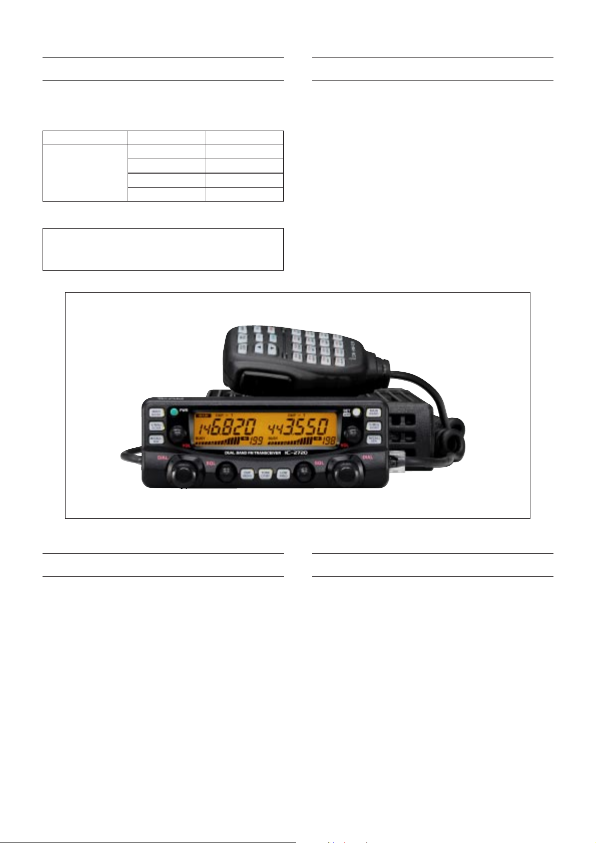
DUAL BAND FM TRANSCEIVER
i2720H
SERVICE
MANUAL
Page 2
INTRODUCTION
This service manual describes the latest service information
for the IC-2720H DUAL BAND FM TRANSCEIVER at the
time of publication
DANGER
NEVER connect the transceiver to an AC outlet or to a DC
power supply that uses more than 16 V. This will ruin the
transceiver.
DO NOT expose the transceiver to rain, snow or any liquids.
DO NOT reverse the polarities of the power supply when
connecting the transceiver.
DO NOT apply an RF signal of more than 20 dBm (100 mW)
to the antenna connector. This could damage the transceiver’s front end.
ORDERING PARTS
Be sure to include the following four points when ordering
replacement parts:
1. 10-digit order numbers
2. Component part number and name
3. Equipment model name and unit name
4. Quantity required
<SAMPLE ORDER>
1110004310 S.IC M62352GP IC-2720H MAIN UNIT 5 pieces
8810009610 Screw FH M2.6
×6 ZK IC-2720H bottom cover 10 pieces
Addresses are provided on the inside back cover for your
convenience.
REPAIR NOTES
1. Make sure a problem is internal before disassembling the
transceiver.
2. DO NOT open the transceiver until the transceiver is
disconnected from its power source.
3. DO NOT force any of the variable components. Turn
them slowly and smoothly.
4. DO NOT short any circuits or electronic parts. An insulated tuning tool MUST be used for all adjustments.
5. DO NOT keep power ON for a long time when the transceiver is defective.
6. DO NOT transmit power into a signal generator or a
sweep generator.
7. ALWAYS connect a 50 dB to 60 dB attenuator between
the transceiver and a deviation meter or spectrum analyzer when using such test equipment.
8. READ the instructions of test equipment thoroughly
before connecting equipment to the transceiver.
To upgrade quality, any electrical or mechanical parts and
internal circuits are subject to change without notice or
obligation.
MODEL
IC-2720H
VERSION
U.S.A.
Korea
S.E.Asia
Export
SYMBOL
USA
KOR
SEA
EXP
Page 3

TABLE OF CONTENTS
SECTION 1 SPECIFICATIONS
SECTION 2 INSIDE VIEWS
SECTION 3 DISASSEMBLY INSTRUCTIONS
SECTION 4 CIRCUIT DESCRIPTION
4 - 1 RECEIVER CIRCUITS . . . . . . . . . . . . . . . . . . . . . . . . . . . . . . . . . . . . . . . . . . . . . . . . . . . . . . . . . . . .4 - 1
4 - 2 TRANSMITTER CIRCUITS . . . . . . . . . . . . . . . . . . . . . . . . . . . . . . . . . . . . . . . . . . . . . . . . . . . . . . . . .4 - 5
4 - 3 PLL CIRCUITS . . . . . . . . . . . . . . . . . . . . . . . . . . . . . . . . . . . . . . . . . . . . . . . . . . . . . . . . . . . . . . . . . .4 - 6
4 - 4 POWER SUPPLY CIRCUITS . . . . . . . . . . . . . . . . . . . . . . . . . . . . . . . . . . . . . . . . . . . . . . . . . . . . . . .4 - 8
4 - 5 CPU PORT ALLOCATIONS . . . . . . . . . . . . . . . . . . . . . . . . . . . . . . . . . . . . . . . . . . . . . . . . . . . . . . .4 - 10
SECTION 5 PARTS LIST
SECTION 6 MECHANICAL PARTS AND DISASSEMBLY
SECTION 7 SEMI-CONDUCTOR INFORMATION
SECTION 8 BOARD LAYOUTS
8 - 1 CONTROL UNIT . . . . . . . . . . . . . . . . . . . . . . . . . . . . . . . . . . . . . . . . . . . . . . . . . . . . . . . . . . . . . . . . 8 - 1
8 - 2 MAIN UNIT . . . . . . . . . . . . . . . . . . . . . . . . . . . . . . . . . . . . . . . . . . . . . . . . . . . . . . . . . . . . . . . . . . . . .8 - 3
8 - 3 VCO UNIT . . . . . . . . . . . . . . . . . . . . . . . . . . . . . . . . . . . . . . . . . . . . . . . . . . . . . . . . . . . . . . . . . . . . .8 - 5
SECTION 9 BLOCK DIAGRAM
SECTION 10 VOLTAGE DIAGRAMS
10 - 1 CONTROL UNIT . . . . . . . . . . . . . . . . . . . . . . . . . . . . . . . . . . . . . . . . . . . . . . . . . . . . . . . . . . . . . . . 10 - 1
10 - 2 MAIN AND VCO UNITS . . . . . . . . . . . . . . . . . . . . . . . . . . . . . . . . . . . . . . . . . . . . . . . . . . . . . . . . . .10 - 2
Page 4

1 - 1
SECTION 1 SPECIFICATIONS
All stated specifications are subject to change without notice or obligation.
M GENERAL
• Frequency range :
LEFT SIDE
RIGHT SIDE
*1Guaranteed 144.000 – 146.000 MHz only, *2Guaranteed 144.000 – 148.000 MHz only,
*
3
Guaranteed 430.000 – 440.000 MHz only; *4Guaranteed 440.000 – 450.000 MHz only
*
5
Not guaranteed range
• Mode : FM, AM (AM range is 118.0 – 135.995 MHz and Rx only for [USA] and [EXP].)
• Nomber of memory channel : 212 (including 2 call channels and 10 scan edges)
• Usable temperature range : –10˚C to +60˚C; +14˚F to +140˚F
• Frequency resolution : 5, 10, 12.5, 15, 20, 25, 30 and 50 kHz
• Frequency stability : ±10 ppm (–10˚C to +60˚C; +14˚F to +140˚F)
• Power supply requirement : 13.8 V DC ±15 % (negative ground)
• Current drain
(at 13.8 V DC) : Receive Standby (squelched) 1.2 A
Max. audio output 1.8 A
Transmit at VHF 50 W/UHF 35 W 12.0 A/11.0 A
• Antenna connector : SO-239 (50 Ω)
• DATA connector : Mini DIN 6 pin
• Dimensions : Controller 140(W)
×50(H)×27(D) mm; 51⁄2(W)×131⁄32(H)×11⁄16(D) inch
(projections not included) Main unit 140(W)×40(H)×187(D) mm; 5
1
⁄2(W)×19⁄16(H)×73⁄8(D) inch
• Weight : Controller 150 g; 5.29 oz
Main unit 1.4 kg; 3.0 lb
M TRANSMITTER
• Output power : VHF 50 W/25 W/5 W (selectable)
UHF 35 W/25 W/5 W (selectable)
• Modulation system : Variable reactance frequency
• Maximum frequency deviation: ±5.0 kHz
• Spurious emissions : Less than –60 dB
• Microphone connector : 8-pin modular jack (600 Ω)
M RECEIVER
• Receive system : Double-conversion superheterodyne
• Intermediate frequency : 1st IF 38.85 MHz/46.05 MHz
(Left/right side band) 2nd IF 450 kHz/455 kHz
• Sensitivity : Less than 0.18 µV (at 12 dB SINAD)
• Squelch sensitivity : Less than 0.13 µV (at threshold)
• Selectivity : More than 12 kHz/–6 dB (Wide); More than 6 kHz/–6 dB (Narrow)
Less than 30 kHz/–60 dB (Wide); Less than 20 kHz/–60 dB (Narrow)
• Spurious and image rejection : More than 60 dB
• Audio output power
(at 13.8 V) : More than 2.4 W at 10% distortion with an 8 Ω load
• External speaker connector : 2-conductor 3.5(d) mm (
1
⁄8")/8 Ω
VERSION
[KOR]
[SEA]
[EXP]
[USA]
RX (MHz)
144.000–146.000, 430.000–440.000
136.000–179.995*2, 430.000–440.000
118.000–549.995*
2
118.000–549.995*
2, *4
TX (MHz)
144.000–146.000, 430.000–440.000
140.000–150.000*
2
, 430.000–440.000
136.000–174.000*2, 400.000–479.000*
3
144.000–148.000, 430.000–450.000*
4
VERSION
[KOR]
[SEA]
[EXP]
[USA]
RX (MHz)
144.000–146.000, 430.000–440.000
136.000–173.995*2, 430.000–440.000
118.000–179.995*
2
, 375.000–549.995*
3
810.000–999.990*
5
118.000–174.000*2, 375.000–549.995*4,
810.000–824.000*5, 849.000–869.000*5,
894.000–999.990*
5
TX (MHz)
144.000–146.000, 430.000–440.000
140.000–150.000*
2
, 430.000–440.000
136.000–174.000*2, 400.000–479.000*
3
144.000–148.000, 430.000–450.000*
4
Page 5
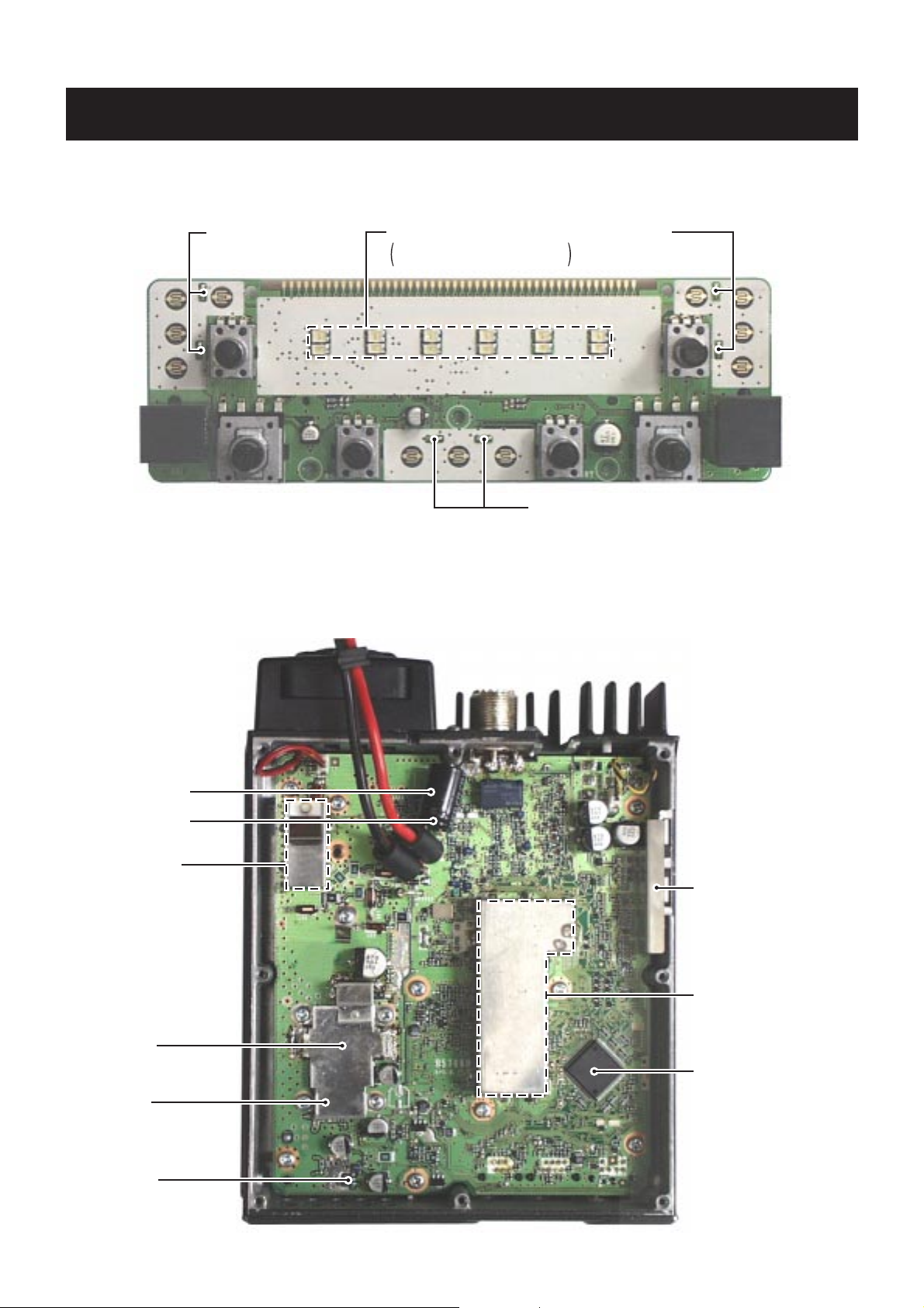
SECTION 2 INSIDE VIEWS
2 - 1
• CONTROL UNIT (TOP VIEW)
• MAIN UNIT (TOP VIEW)
Key back light
Key back light
(DS14, DS15: LN1371G)
(DS14, DS15: LN1371G)
LCD back light
LCD back light
DS1-3, DS7-9: SML-010MT
DS1-3, DS7-9: SML-010MT
DS4-6, DS10-12: SML-020MLT
DS4-6, DS10-12: SML-020MLT
Key back light
Key back light
(DS15, DS18: LN1371G)
(DS15, DS18: LN1371G)
Key back light
Key back light
(DS16, DS17: LN1371G)
(DS16, DS17: LN1371G)
VHF RX Pre amplifier
(Q33: 3SK272)
UHF RX Pre amplifier
(Q24: 3SK274)
VHF low-pass filter
VHF low-pass filter
Power amplifier
Power amplifier
(Q27: RD70HVF1)
(Q27: RD70HVF1)
Drive amplifier
Drive amplifier
(Q25: 2SK3075)
(Q25: 2SK3075)
Drive amplifier
TX pre-amplifier
(Q25: 2SK3075)
(Q16: 2SK2854)
AF amplifier
AF amplifier
(IC2012: LA4445)
(IC2012: LA4445)
VCO unit
VCO unit
Main CPU
Main CPU
(IC2013: HD64F2144AFA20)
(IC2013: HD64F2144AFA20)
Page 6
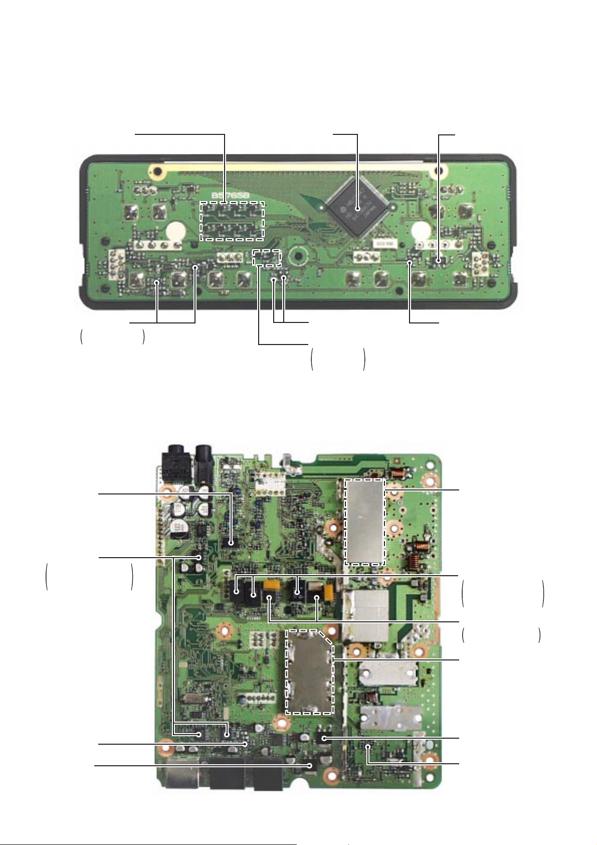
• CONTROL UNIT (BOTTOM VIEW)
• MAIN UNIT (BOTTOM VIEW)
2 - 2
Dimmer
Dimmer circuit
(Q6-Q13: 2SC4116)
Mic amplifier
Mic amplifier
IC5: TA75S558F
IC5: TA75S558F
Q15: 2SC4116
Q15: 2SC4116
Sub CPU
Control unit CPU
(IC4: HD6473847RH)
(IC4: HD6473847RH)
Data comparator
Data comparator
(IC1: TA75S01F)
(IC1: TA75S01F, D2: MA8047)
+8V regurator
+8V regurator
Q1: 2SC4116
(Q1: 2SC4116)
Q3: 2SA1586
D1: MA8091
+5V regurator
+5V regurator
(IC3: TA78L05F)
(IC3: TA78L05F)
Reset IC
Reset IC
(IC2: S-80945CLMC)
(IC2: S-80945CLMC)
D/A converter
D/A converter
(IC1: M62352GP)
(IC1: M62352GP)
Analog switch
Analog switch
IC2007: BU4066BCFV
IC2007: BU4066BCFV
IC2010: BU4066BCFV
IC2008: BU4066BCFV
IC2010: BU4066BCFV
+8V regurator
+8V regurator
(IC2003: TA7808F)
(IC2003: TA7808F)
Mic amplifier
Mic amplifier
(IC2014: TA75S558F)
(IC2014: TA75S558F)
UHF low-pass filter circuit
Ceramic bandpass filters
FI1000: CFWM450E
FI1001: CFWS450HT
FI1002: CFWM455E
FM IF IC
IC1001: TA31136FN
IC1004: TA31136FN
PLL circuit
+5V regurator
(IC2002: TA7805F)
APC amplifier
(IC2: TA75S01F)
Page 7
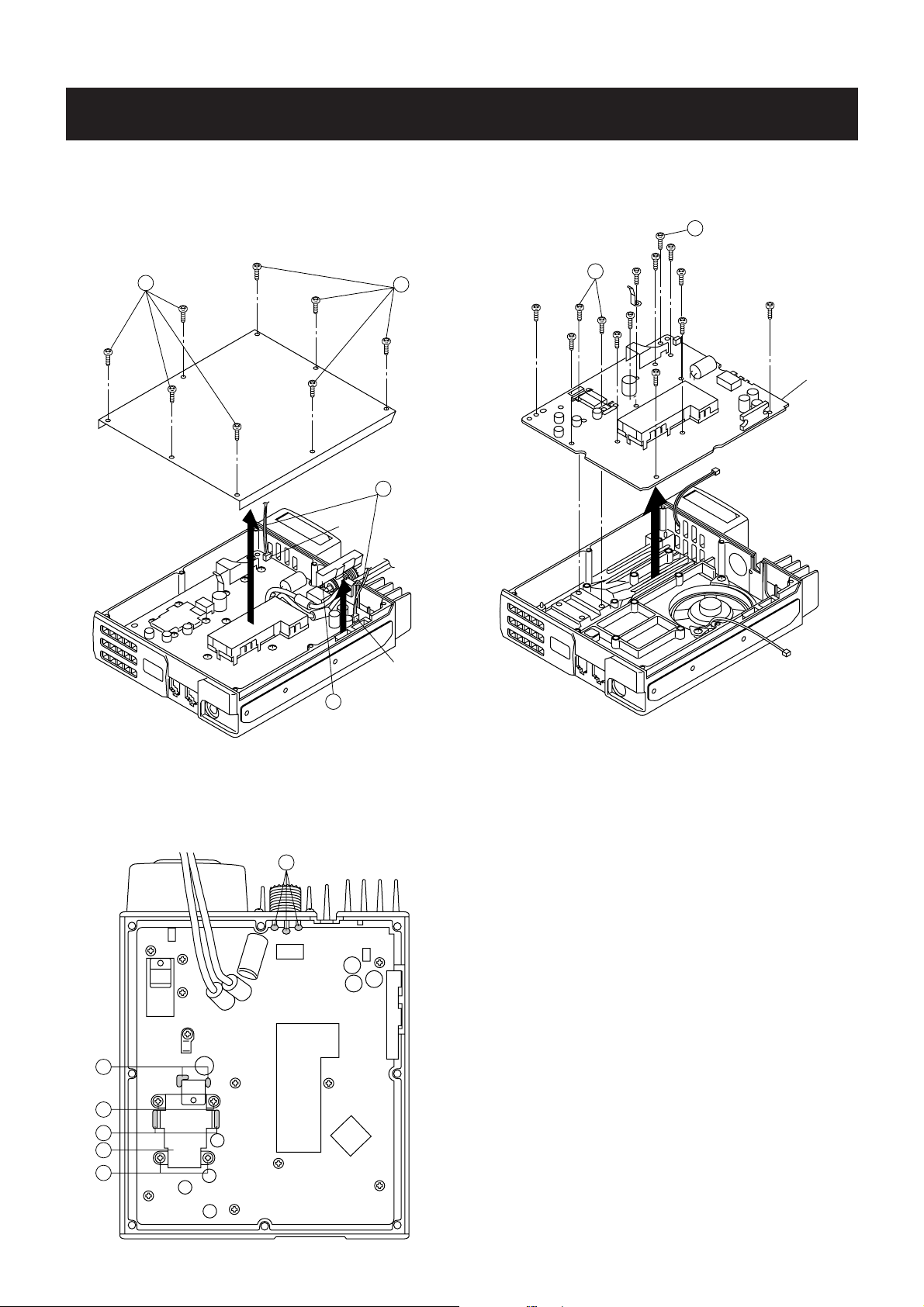
SECTION 3 DISASSEMBLY INSTRUCTIONS
• Removing the MAIN unit
➀
Unscrew 8 screws A, and remove the cover.
➁ Disconnect two cables B from J1 and J2007.
➂ Remove the clip c.
➃ Unsolder 3 points E.
➄ Unscrew 4 screws F.
➅ Unsolder 4 points G, and remove the cover H.
➆ Unscrew 2 screws I.
➇ Unscrew 12 screws J, and remove MAIN unit.
3 - 1
A
J1
J
I
A
MAIN UNIT
B
C
E
G
F
G
H
F
J2007
Page 8
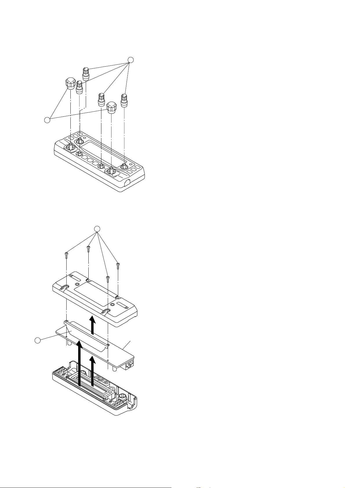
• Removing the CONTROL unit
➀
Remove 6 knobs A.
➁ Unscrew 4 screws B, and remove the cover.
➂ Remove the plate C, and remove CONTROL unit.
3 - 2
A
A
B
C
CONTROL UNIT
Page 9

4 - 1
SECTION 4 CIRCUIT DESCRIPTION
4-1 RECEIVER CIRCUITS
4-1-1 TRIPLEXER AND RX BAND SWITCHING
CIRCUITS (MAIN UNIT)
The transceiver has a triplexer (low-pass and high-pass filters) on the first stage from the antenna connector to separate the signals into VHF and UHF signals. The RF signals
from the antenna connector are applied to the tripler or RX
band swtich circuits.
• RF SIGNALS V-V (118 MHz–180 MHz), U-V (136
MHz–174 MHz)
The V-V and U-V RF signals from the antenna connector
pass through the low-pass filter (L76, L77, L80, C205, C209,
C242, C243, C264), and then applied to the TX/RX switching
circuit (D42, D46, D52, D67, D2049). The filtered signals are
amplified at the pre-amplifier (Q33), and are applied to the
left side or right side displayed RX circuits.
• RF SIGNALS U-U, V-U2 (375 MHz–550 MHz)
The U-U and V-U2 RF signals from the antenna connector
pass through the high-pass filter (L78, L81, C206, C210,
C213, C265), and then applied to the TX/RX switching circuit
(D55, D64, D65, D2050) via the SWR detector (D50, D58).
The filtered signals are amplified at the pre-amplifier (Q24),
and are applied to the left side or right side displayed RX circuits.
• RF SIGNALS U-U3 (810 MHz–1000 MHz)
The U-U3 RF signals from the antenna connector pass
through the two low-pass filters (L76, L77, L80, C205, C209,
C242, C243, C264, L87, L88, C266–C268), and are then
applied to the RX band swtiching circuit (D2061). The filtered
signals are amplified at the RF amplifier (Q18), and are
applied to the right side displayed RX circuits.
• RF SIGNALS V220 (174 MHz–260 MHz), V-U1 (225
MHz–375 MHz)
The V220 and V-U1 RF signals from the antenna connector
are applied to the RX band swtiching circuit (Q34, D66, RL1),
and are applied to the left side displayed RX circuit.
4-1-2 RF CIRCUIT FOR LEFT SIDE DISPLAY
(MAIN UNIT)
• RF SIGNALS V-V (118 MHz–180 MHz)
The amplified signals are applied to the RF amplifier (Q29)
after being passed through the attenuator (D59) and bandpass filter (D47, D53). The signals are applied to the RX
band switching circuit (D28) via the another bandpass filter
(D32, D39) to supress the unwanted signals.
• RF SIGNALS V220 (174 MHz–260 MHz)
The signals are applied to the RF amplifier (Q31) after being
passed through the RX band switching circuit (D62) and
bandpass filter (D51). The amplified signals are applied to
the RX band switching circuit (D28) via the another bandpass
filter (D34) to supress the unwanted signals and attenuator
(R195–R197).
• RF SIGNALS V-U1 (225 MHz–375 MHz)
The signals are applied to the RF amplifier (Q32) after being
passed through the RX band switching circuit (D63) and
bandpass filter (D49). The amplified signals are applied to
the RX band switching circuit (D31) via the attenuator
(R198–R200) and another bandpass filter (D35) to supress
the unwanted signals.
• RF SIGNALS V-U2 (375 MHz–550 MHz)
The amplified signals are applied to the RF amplifier (Q20)
after being passed through the attenuator (D25) and bandpass filter (D23, D73). The signals are applied to the RX
band switching circuit (D9) via the another bandpass filter
(D13, D17) to supress the unwanted signals.
BPF BPF
ANTENNA
1st mixer
(IC1005)
1st LO
to 2nd mixer
circuit
ATT
RX
SW
RF
PRE
BPF BPF
ATT
RX
SW
RF
PRE
BPF BPF
ATT
RX
SW
RX
SW
RX
SW
RF
BPF BPF
ATT
RX
SW
RX
SW
RF
D59Q29
V-V (118 MHz—174 MHz)
V220 (174 MHz—260 MHz)
V-U1 (225 MHz—375 MHz)
V-U2 (375 MHz—550 MHz)
D28 D32, D39 D47, D53
D62Q31D30 D34 D51
D63Q32D31 D35 D49
Q33
Q34, D66,
RL1
D25Q20D9 D13, D17 D23, D73 Q24
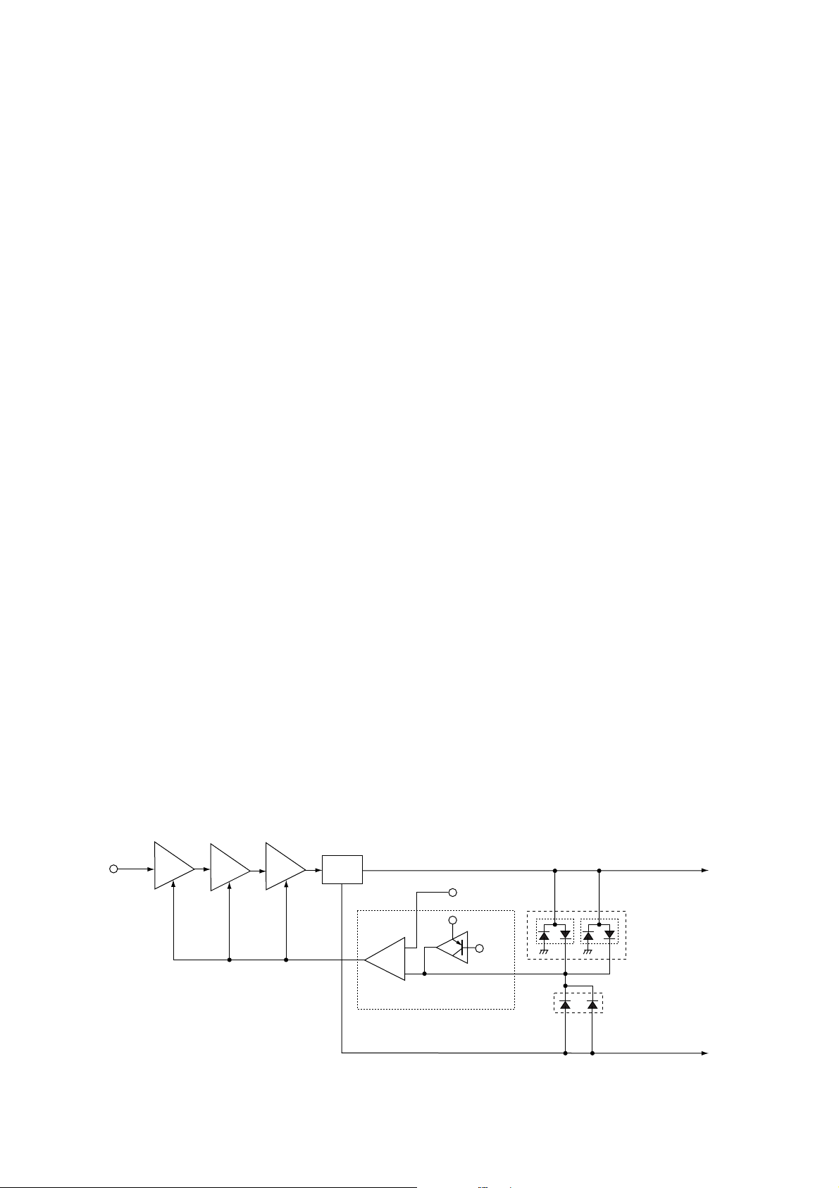
• RF CIRCUIT FOR LEFT SIDE DISPLAY
Page 10
4 - 2
The signals from the RX band swtiching circuits are then
applied to the left side displayed 1st mixer circuit (IC1005, pin
6).
4-1-3 1ST MIXER AND 1ST IF CIRCUIT FOR LEFT
SIDE DISPLAY (MAIN UNIT)
The 1st mixer circuit converts the received RF signals to a
fixed frequency of the 1st IF signal with a PLL output frequency. By changing the PLLfrequency, only the desired frequency will pass through the bandpass filter at the next stage
of 1st mixer circuit.
The RF signals are mixed with 1st LO signals at the 1st mixer
(IC1005) to produce a 38.85 MHz 1st IF signal. The 1st IF
signal is output from pin 1, and passed through the crystal
bandpass filter (FI1003) to suppress unwanted harmonic
components. The filtered signal is amplified at the IF amplifier (Q1040) after being passed through the limiter circuit
(D1021). The amplified signal is applied to the 2nd mixer circuit (IC1001).
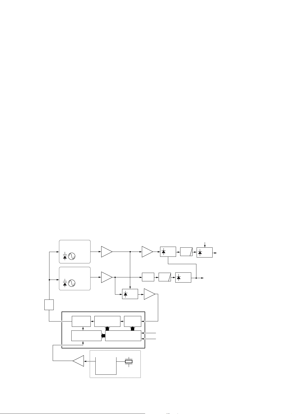
4-1-4 2ND IF AND DEMODULATOR CIRCUITS FOR
LEFT SIDE DISPLAY (MAIN UNIT)
The 2nd mixer circuit converts the 1st IF signal to a 2nd IF
signal. A double conversion superheterodyne system (which
converts receive signal twice) improves the image rejection
ratio and obtains stable receiver gain.
The FM IC IC (IC1001) contains the 2nd mixer, limiter and
noise amplifiers, quadrature detector, S-meter detector,
active filter circuits, etc. A 2nd LO signal (38.4 MHz) is produced at the PLL circuit by dividing it’s reference frequency.
The 38.85 MHz 1st IF signal from the IF amplifier (Q1040) is
applied to the 2nd mixer section of the FM IF IC (IC1001, pin
16), and is mixed with the 2nd LO signal (38.4 MHz) to be
converted to a 450 kHz 2nd IF signal.
The 2nd IF signal is applied to the each demodulator circuits
by AM or FM mode.
• FM MODE
The 2nd IF signal is output from the FM IF IC (IC1001, pin 3)
and passes through the ceramic bandpass filter (FI1001).
The filtered signal is fed back to the IC, and amplified at the
limiter amplifier section (pin 5), then demodulated into AF signals at the quadrature detector section (pins 10, 11). The
detected AF signals are output from pin 9 and are applied to
the AF circuit via the AM/FM selector circuit (IC2015, pins 7,
1).
• AM MODE
The 2nd IF signal is output from the FM IF IC (IC1001, pin 3)
and passes through the ceramic bandpass filter (FI1000).
The filtered signal is applied to the AM detector circuit
(Q1017) to convert into AF signals, and then amplified at the
Q1014 (pins 5, 1). The amplified AF signals are applied to the
AF circuit via the AM/FM selector circuit (IC2015, pins 6, 1).
4-1-5 AF AMPLIFIER CIRCUIT FOR LEFT SIDE
DISPLAY (MAIN UNIT)
The AF amplifier circuit amplifies the demodulated AF signals
to drive a speaker.
The AF signals pass through the AF mute switch (Q1010),
and are then applied to the electric volume control circuit
(IC2011, pin 1) as “VAFO” signal after being passed through
the low-pass filter (Q1007). The level controlled AF signals
are output from pin 2, and are then applied to the AF power
amplifier (IC2012, pin 2) via the “VOUT1” signal. The power
amplified AF signals are applied to the internal speaker (SP1)
via the [EXT SP] jack (J2005).
The electronic volume control circuit controls AF gain, therefore, the AF output level is according to the [VOL] setting and
also the squelch conditions.
4-1-6 NOISE SQUELCH CIRCUIT FOR LEFT SIDE
DISPLAY (MAIN UNIT)
• NOISE SQUELCH
A noise squelch circuit cuts out AF signals when no RF signal is received. By detecting noise components in the AF signal, the squelch circuit switches the AF mute switch.
16
Limiter
amp.
2nd IF filter
450 kHz
PLL IC
IC1
X1
12.8 MHz
38.4 MHz
RSSI
IC1001 TA31136F
13
1st IF (38.85 MHz)
from Q1040
"L_RSSI" signal to the CPU
(IC2013, pin 33)
11
10
9
8
7
5
3
2
2
VCO UNIT
1
Active
filter
FI1001
FI1000
Noise
detector
FM
detector
Noise
comp.
"L_SQL" signal to the CPU
(IC2013, pin 40)
12
R1124
R1291
C1108
C1100
R1108
C1078
C1085
C1084
C1097
AM
DET.
IF
amp.
C1069
R1092
R1109
R1114
L_R5
X1001
FM or WFM AF signal
to AM/FM selector
AM AF signal
to AM/FM selector
Mixer
2nd
Q1049
from Q1013
3
C1271
• 2ND IF AND DEMODULATOR CIRCUIT FOR LEFT SIDE DISPLAY
Page 11
4 - 3
A portion of the AF signals from the FM IF IC (IC1001, pin 9)
are applied to the active filter section (IC1001, pin 8). The
active filter section amplifies and filters noise components.
The filtered signals are applied to the noise detector section
and output from the IC1001 (pin 14) as the “L_SQL” signal.
The “L_SQL” signal from IC1001 (pin 14) is applied to the
CPU (IC2013, pin 40). The CPU analyzes the noise condition
and outputs the “L_DET_MUTE” signal to the AF mute switch
(Q1010).
• TONE SQUELCH
The tone squelch circuit detects AF signals and opens the
squelch only when receiving a signal containing a matching
subaudible tone (CTCSS). When tone squelch is in use, and
a signal with a mismatched or no subaudible tone is
received, the tone squelch circuit mutes the AF signals even
when noise squelch is open.
A portion of the AF signals from the FM IF IC (IC1001, pin 9)
passes through the low-pass filter (Q1003) to remove AF
(voice) signals. The filtered signal is applied to the CTCSS
decoder which is inside the CPU (IC2013, pin 41) via the
“L_DTCS_IN” line to control the AF mute switch (Q1010).
4-1-7 RF CIRCUIT FOR RIGHT SIDE DISPLAY
(MAIN UNIT)
• RF SIGNALS U-V (136 MHz–174 MHz)
The amplified signals are applied to the RF amplifier (Q30)
after being passed through the attenuator (D60) and bandpass filter (D48, D54). The signals are applied to the RX
band switching circuit (D29) via the another bandpass filter
(D33, D40) to supress the unwanted signals.
• RF SIGNALS U-U3 (810 MHz–1000 MHz)
The signals are applied to the RF amplifier (Q18) after being
passed through the RX band switching circuit (D2061). The
amplified signals pass through the attenuator (L19, C20,
C46, C51, R178–R180) and high-pass filter (L20, C278,
C279), and are then applied to the another RF amplifier
(Q35) again. The signals pass through the attenuator (L10,
C15, C280, R183–R185) and RX bamd switching circuit
(D11).
• RF SIGNALS V-U2 (375 MHz–550 MHz)
The amplified signals are applied to the RF amplifier (Q19)
after being passed through the attenuator (D24) and bandpass filter (D22, D72). The signals are applied to the RX
band switching circuit (D8) via the another bandpass filter
(D12, D16) to supress the unwanted signals.
The signals from the RX band swtiching circuits are then
applied to the right side displayed 1st mixer circuit (IC1006,
pin 6).
4-1-8 1ST MIXER AND 1ST IF CIRCUIT FOR RIGHT
SIDE DISPLAY (MAIN UNIT)
The 1st mixer circuit converts the received RF signals to a
fixed frequency of the 1st IF signal with a PLL output frequency. By changing the PLLfrequency, only the desired frequency will pass through the bandpass filter at the next stage
of 1st mixer circuit.
The RF signals are mixed with 1st LO signals at the 1st mixer
(IC1006) to produce a 46.05 MHz 1st IF signal. The 1st IF
signal is output from pin 1, and passed through the crystal
bandpass filter (FI1004) to suppress unwanted harmonic
components. The filtered signal is amplified at the IF amplifier (Q1041) after being passed through the limiter circuit
(D1022). The amplified signal is applied to the 2nd mixer circuit (IC1004).
4-1-9 2ND IF AND DEMODULATOR CIRCUITS FOR
RIGHT SIDE DISPLAY (MAIN UNIT)
The 2nd mixer circuit converts the 1st IF signal to a 2nd IF
signal. A double conversion superheterodyne system (which
converts receive signal twice) improves the image rejection
ratio and obtains stable receiver gain.
The FM IC IC (IC1004) contains the 2nd mixer, limiter and
noise amplifiers, quadrature detector, S-meter detector,
active filter circuits, etc. A2nd LO signal (45.595 MHz) is produced at the PLL circuit by dividing it’s reference frequency.
BPF BPF
ANTENNA
1st mixer
(IC1006)
1st LO
to 2nd mixer
circuit
ATT
RX
SW
RF
PRE
BPF BPF
ATT
RX
SW
RF
PRE
HPF
ATT ATT
RX
SW
RX
SW
D60Q30
U-V (136 MHz 174 MHz)
U-U3 (810 MHz 1000 MHz)
V-U2 (375 MHz 550 MHz)
D29 D33, D40 D48, D54
D2061
RF
Q35
RF
Q18D11
Q33
D24Q19D8 D12, D16 D22, D72 Q24
• RF CIRCUIT FOR RIGHT SIDE DISPLAY
Page 12
4 - 4
The 46.05 MHz 1st IF signal from the IF amplifier (Q1041) is
applied to the 2nd mixer section of the FM IF IC (IC1004, pin
16), and is mixed with the 2nd LO signal (45.595 MHz) to be
converted to a 455 kHz 2nd IF signal.
The 2nd IF signal is applied to the each demodulator circuits
by AM or FM mode.
• FM MODE
The 2nd IF signal is output from the FM IF IC (IC1004, pin 3)
and passes through the ceramic bandpass filter (FI1002).
The filtered signal is fed back to the IC, and amplified at the
limiter amplifier section (pin 5), then demodulated into AF signals at the quadrature detector section (pins 10, 11). The
detected AF signals are output from pin 9 and are applied to
the AF circuit via the AM/FM selector circuit (IC2016, pins 7,
1).
• AM MODE
The 2nd IF signal is output from the FM IF IC (IC1001, pin 3)
and passes through the ceramic bandpass filter (FI1002).
The filtered signal is applied to the AM detector circuit
(Q1025) to convert into AF signals, and then amplified at the
Q1022 (pins 5, 1). The amplified AF signals are applied to the
AF circuit via the AM/FM selector circuit (IC2016, pins 6, 1).
4-1-10 AF AMPLIFIER CIRCUIT FOR RIGHT SIDE
DISPLAY (MAIN UNIT)
The AF amplifier circuit amplifies the demodulated AF signals
to drive a speaker.
The AF signals pass through the AF mute switch (Q1011),
and are then applied to the electric volume control circuit
(IC2011, pin 8) as “UAFO” signal after being passed through
the low-pass filter (Q1008). The level controlled AF signals
are output from pin 7, and are then applied to the AF power
amplifier (IC2012, pin 5) via the “VOUT2” signal. The power
amplified AF signals are applied to the internal speaker (SP1)
via the [EXT SP] jack (J2004).
When no plug is connected to the jack, the signals are fed
back to the UHF audio input (IC2012, pin 2) and combined
with the UHF audio. The mixed audio is applied to the other
external speaker jack (J2005) and then to the internal speaker.
The electronic volume control circuit controls AF gain, therefore, the AF output level is according to the [VOL] setting and
also the squelch conditions.
4-1-11 NOISE SQUELCH CIRCUIT FOR RIGHT SIDE
DISPLAY (MAIN UNIT)
• NOISE SQUELCH
A noise squelch circuit cuts out AF signals when no RF signal is received. By detecting noise components in the AF signal, the squelch circuit switches the AF mute switch.
A portion of the AF signals from the FM IF IC (IC1004, pin 9)
are applied to the active filter section (IC1004, pin 8). The
active filter section amplifies and filters noise components.
The filtered signals are applied to the noise detector section
and output from the IC1004 (pin 14) as the “R_SQL” signal.
The “R_SQL” signal from IC1004 (pin 14) is applied to the
CPU (IC2013, pin 38). The CPU analyzes the noise condition
and outputs the “R_DET_MUTE” signal (pin 58) to the AF
mute switch (Q1011).
• TONE SQUELCH
The tone squelch circuit detects AF signals and opens the
squelch only when receiving a signal containing a matching
subaudible tone (CTCSS). When tone squelch is in use, and
a signal with a mismatched or no subaudible tone is
received, the tone squelch circuit mutes the AF signals even
when noise squelch is open.
A portion of the AF signals from the FM IF IC (IC1004, pin 9)
passes through the low-pass filter (Q1004) to remove AF
(voice) signals. The filtered signal is applied to the CTCSS
decoder which is inside the CPU (IC2013, pin 39) via the
“R_DTCS_IN” line to control the AF mute switch (Q1011).
16
Limiter
amp.
2nd IF filter
455 kHz
X1002
45.595 MHz
RSSI
IC1004 TA31136F
14
1st IF (46.05 MHz)
from Q1041
"R_RSSI" signal to the CPU
(IC2013, pin 32
11
10
9
8
7
5
3
2
Active
filter
FI1002
Noise
detector
FM
detector
Noise
comp.
"R_SQL" signal to the CPU
(IC2013, pin 38)
12
R1187
C1148
C1145
R1174
C1131
C1035
C1034
Q1022,
Q1025
C1044
AM
DET.
C1122
R1164
R1168
R1175
R1179
R_R5
X1002
FM AF signal
to AM/FM selector
AM AF signal
to AM/FM selector
Mixer
2nd
• 2ND IF AND DEMODULATOR CIRCUIT FOR RIGHT SIDE DISPLAY
Page 13

4-2 TRANSMITTER CIRCUITS
4-2-1 MICROPHONE AMPLIFIER CIRCUIT
(MAIN AND CONTROL UNITS)
The microphone amplifier circuit amplifies audio signals from
the microphone to a level needed for the modulation circuit.
The microphone amplifier circuit is commonly used for the
both VHF and UHF bands.
• THE AF SIGNALS FROM THE MAIN UNIT
The AF signals from the microphone (J2001, pin 6) pass
through the high-pass filter (Q2028), and are then applied to
the microphone amplifier (IC2014, pin 3). The amplified signals are applied to the analog switch (IC2008, pin 1).
The microphone sensitivity is controlled by the microphone
sensitivity controller (Q2023) via the “MIC_SENS” line from
the CPU (IC2023).
•THE AF SIGNALS FROM THE CONTROL UNIT
The AF signals from the microphone (CONTROLunit; J1, pin
6) are applied to the microphone amplifier (Q15, IC5 pin 3).
The amplified signals pass through the J2, pin 2 via the “MIC”
line, and are then applied to the analog switch (IC2008, pin
4).
The microphone sensitivity is controlled by the microphone
sensitivity controller (Q2022) via the “MIC_SENS” line from
the CPU (IC2023).
The each AF signals (from IC2008, pins 1, 4) are applied to
the IDC limiter amplifier section (IC1000a, pin 3), and then
pass through the de-emphasis circuit (C1036, R1050). The
signals pass through the splatter filter (IC1000d, pins13, 14),
and are then applied to the buffer amplifier (IC1000c, pin 9).
The amplified signals are applied to the D/A convertor IC
(IC1009, pin 12) to control the modulation level.
• THE DATA SIGNALS
(1) 9600 bps mode
The data signals from the J2003, pin 1 are applied to the
analog switch (IC2007, pin 4) after being passed through the
limiter circuit (D2012). The signals pass through another analog swtich (IC2008, pins 9 and 8), and are then applied to the
buffer amplifier (IC100c, pin 9) via the “DATAMOD” line. The
amplified signals are applied to the D/Aconvertor IC (IC1009,
pin 12) to control the modulation level.
(2) 1200 bps mode
The data signals from the J2003, pin 1 are applied to the
analog switch (IC2007, pin 4) after being passed through the
limiter circuit (D2012). The signals pass through another analog swtich (IC2008, pins 10 and 11), and are then applied to
the IDC limiter amplifier section (IC1000a, pin 3). The signals
pass through the de-emphasis circuit (C1036, R1050) and
splatter filter (IC1000d, pins13, 14). The signals are amplified
at the buffer amplifier (IC1000c, pin 9), and are then applied
to the D/A convertor IC (IC1009, pin 12) to control the modulation level.
The AF or data signals are applied to the each VCO circuit
from the D/A convertor IC (IC1009, pin 11) as “MOD” signal.
4-2-2 VHF MODULATION CIRCUIT
(MAIN AND VCO UNITS)
The modulation circuit modulates the oscillating signal (RF
signal) using the microphone audio signals.
The “MOD” signal from the D/A convertor IC (IC1009, pin 11)
changes the reactance of D5 (VCO unit) to modulate the
oscillated signal at the VHF-VCO circuit (VCO unit; Q6). The
modulated signal is amplified at the buffer amplifiers (VCO
unit; Q7, Q8), and then passes through the VCO swtich
(VCO unit; D12, D13). The TX LO signal passes through the
low-pass filter (L90, L91, C245–C247) and attenuator
(C2134, R2216–C2218), and is then applied to the TX switch
(D77) via the “VHF_YGR” line. The signal is applied to the
drive/power amplifier circuits.
4-2-3 UHF MODULATION CIRCUIT (MAIN UNIT)
The “MOD” signal from the D/A convertor IC (IC1009, pin 11)
changes the reactance of D1018 to modulate the oscillated
signal at the UHF-VCO circuit (Q1039). The modulated signal is amplified at the buffer amplifiers (Q1044, Q1047), and
then passes through the VCO swtich (D2059, D2060). The
TX LO signal passes through the high-pass filter (L1079,
C2183, C2184), and is then applied to the TX switch (D78)
via the “UHF_YGR” line. The signal is applied to the
drive/power amplifier circuits.
4-2-4 DRIVE/POWER AMPLIFIER CIRCUITS
(MAIN UNIT)
The drive amplifier circuit amplifies the VCO oscillated signal
to the needed level at the power amplifier. Q27 is a power
module which provides stable 50 W (UHF is 35 W) output
power with a 13.8 V DC power source.
The RF signal from the TX switch (D77; VHF, D78; UHF) is
amplified at the buffer amplifier (Q38), and is then applied to
the pre-amplifier (Q16). The amplified signal is amplified at
the pre-drive (Q21) and drive amplifier (Q25), and then
applied to the power amplifier (Q27) to obtain 50 W (UHF is
35 W) of RF power.
• VHF RF SIGNAL
The amplified signal passes throught the low-pass filter (D36,
D2070), and is then applied to the SWR detector (D57, D61).
The signal is applied to the TX/RX switch (D42), and passes
through the low-pass filter (L76, L77, L80, C205, C209,
C242, C243, C264) to suppress high harmonics components. The signal is applied to the antenna connector after
being passed through the reverse power detector circuit
(D70, D71).
• UHF RF SIGNAL
The amplified signal passes throught the TX/RX swtich (D37,
D38, D41, D43–D45, D68), and is then applied to the SWR
detector (D50, D58). The signal passes through the highpass filter (L78, L81, C206, C210, C213, C265) to suppress
high harmonics components. The signal is applied to the
antenna connector after being passed through the reverse
power detector circuit (D70, D71).
The detected voltage at the reverse detector ciruit is applied
to the CPU (IC2013, pin 35) to switch from high power to
middle power automatically when the SWR become worse.
4 - 5
Page 14
4 - 6
4-2-5 APC CIRCUIT (MAIN UNIT)
The APC circuit protects the pre-drive (Q21), drive amplifier
(Q25) and power amplifier (Q27) from a mismatched output
load and stabilizes the output power.
• VHF APC CIRCUIT
The SWR detector circuit (D57, D61) detects forward signals
and reflection signals at D57 and D61 respectively. The
impedance is matched at 50 Ω and is increased when it is
mismatched.
• UHF APC CIRCUIT
The SWR detector circuit (D50, D58) detects forward signals
and reflection signals at D50 and D58 respectively. The
impedance is matched at 50 Ω and is increased when it is
mismatched.
The detected voltage is applied to the diffrential amplifier
(IC2, pin 3) via the “POWER_DET” line, and the power setting voltage from the D/Aconvertor (IC1, pin 12) is applied to
another input (IC2, pin 1) for the reference as “PWRCON”
line.
When antenna impedance is mismatched, the detected voltage exceeds the power setting voltage. The output voltage of
the differential amplifier (IC2, pin 4) controls the input current
of the pre-drive (Q21), drive amplifier (Q25) and power
amplifier (Q27) to reduce the output power.
4-3 PLL CIRCUITS
4-3-1 GENERAL
A PLL circuit provides stable oscillation of the transmit frequency and the receive local frequency. The PLLcircuit compares the phase of the divided VCO frequency to the reference frequency. The PLL output frequency is controlled by a
crystal oscillator and the divided ratio (N-data) of the programmable divider.
4-3-2 PLL CIRCUIT FOR RIGHT SIDE DISPLAY
(MAIN UNIT)
The R-VCO (for right side display) composes of VHF-VCO
and UHF-VCO circuits.
• FROM THE VHF-VCO CIRCUIT
An oscillated signal from the VHF-VCO circuit (Q1038,
D1014, D1015) passes through the buffer amplifiers (Q1043,
Q1016) and VCO switch (D1023) is applied to the PLL IC for
right side display (IC1008, pin 8)
• FROM THE UHF-VCO CIRCUIT
An oscillated signal from the UHF-VCO circuit (Q1038,
D1016–D1018) passes through the buffer amplifiers
(Q1044,Q1016) and VCO switch (D1023) is applied to the
right side diplayed PLL IC (IC1008, pin 8)
And is then prescaled in the PLL IC based on the divided
ratio (N-data). The reference signal is generated at the refenrece oscillator (VCO unit; X1, 12.8 MHz), and is then amplified at the buffer amplifier (Q1012). The reference signal is
also applied to the PLL IC. The PLL IC detects the out-ofstep phase using the reference frequency and outputs it from
pin 16. The output signal is passed through the loop filter
(Q1020, Q1021, D1008) and is then applied to the right side
display VCO circuit as lock voltage.
4-3-3 R-VCO CIRCUIT FOR RIGHT SIDE DISPLAY
(MAIN UNIT)
The VCO circuit for right side display contains a separated
the VHF-VCO (Q1038, D1014, D1015) and UHF-VCO
(Q1039, D1016–D1018) circuits.
• VHF-VCO (RX ONLY)
The oscillated signal at the VHF-VCO circuit is amplified at
the buffer amplifier (Q1043), and then passes through the
attenuator (R2209–R2211, C2123) and low-pass filter
(L1045, L1046, C1207, C1249, C1250, C1289, C1304). The
signal is applied to the 1st mixer circuit for right side display
(IC1006, pin 4) via the VCO switch (D1028) as the 1st LO
signal.
A portion of the signal from the buffer amplifier (Q1043)
passes through the VCO swtich (D1023), and is then amplified at the buffer amplifier (Q1016). The amplified signal is
fed back to the PLLIC (IC1008, pin 8) as the comparison signal.
Pre
drive
Buff.
amp.
Drive
amp.
Q27
Q21
RF signal
from PLL circuit
Q25
TX
SW
TXC
VHF SWR
DETECTOR
(D57, D61)
VHF transmitter signal
to antenna
UHF transmitter signal
to antenna
UHF SWR
DETECTOR
(D50, D58)
8V
Q22
PWRCON
APC CONTROLLER
IC2
• APC CIRCUIT
Page 15
4 - 7
• UHF-VCO
The oscillated signal at the UHF-VCO circuit is amplified at
the buffer amplifiers (Q1044, Q1047), and is then applied to
the VCO switch (D2059, D2060) to divide UHF TX signal
and RX signal.
(1) UHF TX SIGNAL
The TX UHF signal passes through the high-pass filter
(L1079, C2183, C2184) to suppress harmonics components, and is then applied to the TX switch (D78). The signal is applied to the drive/power amplifier circuit.
(2) RX SIGNAL
The 400 MHz band RX signal is applied to the another VCO
switches (D1038 and D1049), and then passes through the
attenuator (R2206–R2208, C2122) and low-pass fiilter
(L1034, L1035, C1258). The filtered signal passes through
the VCO switch (Q1048, D1039), and is then applied to the
1st mixer circuit (IC1006, pin 4) as the 1st LO signal.
The 900 MHz band RX signal passes through the another
VCO switches (D1027 and D1028), and is then amplified at
the buffer amplifier (Q1042). The signal passes through the
attenuator (L1020, C1202, C1206) and low-pass fiilter
(L1021, L1036, C1252, C1259, C1260). The filtered signal
passes through the VCO switch (D1026), and is then
applied to the 1st mixer circuit (IC1006, pin 4) as the 1st LO
signal.
A portion of the signal from the buffer amplifier (Q1044)
passes through the VCO swtich (D1024), and is then amplified at the buffer amplifier (Q1016). The amplified signal is
fed back to the PLL IC (IC1008, pin 8) as the comparison
signal.
4-3-4 PLL CIRCUIT FOR LEFT SIDE DISPLAY
(VCO UNIT)
An oscillated signal from the L-VCO circuit passes through
the buffer amplifiers (Q7, Q1) is applied to the PLL IC for left
side display (IC1, pin 8).
And is then prescaled in the PLL IC based on the divided
ratio (N-data). The reference signal is generated at the
refenrece oscillator (X1, 12.8 MHz). The reference signal is
also applied to the PLL IC. The PLL IC detects the out-ofstep phase using the reference frequency and outputs it
from pin 16. The output signal is passed through the loop filter (Q2, Q3, D2) and is then applied to the left side display
VCO circuit as lock voltage.
4-3-5 L-VCO CIRCUIT FOR LEFT SIDE DISPLAY
(VCO AND MAIN UNITS)
• VHF TX SIGNAL
The oscillated signal at the VCO circuit is amplified at the
buffer amplifiers (Q7 and Q8), and then passes through the
low-pass filter (MAIN unit; L90, L91, C245–C247) and attenuator (R2216–R2218, C2134) via the VCO switch (D12,
D13). The signal is applied to the drive/power amlifier circuit
(MAIN unit) after being passed through the TX swtich (MAIN
unit; D77).
• RX SIGNAL
The oscillated signal at the VCO circuit is amplified at the
buffer amplifiers (Q7, Q8), and is then applied to the VCO
switch (D7–D9, D15). The signal is applied to the normal
oscillating signal, twice oscillating signal or harf oscillating
signal circuit.
Shift register
Prescaler
Phase
detector
Loop
filter
Programmable
divider
Programmable
reference divider
Q1038,
D1014,
D1015
VHF VCO for
right side display
Buff.
Q1016
Q1043
Buff.
Q1012
D1028
Q1020,
Q1022,
D1008
9
10
PLLCK
IC1008 (PLL IC for right side display)
PLLDATA
1
15
8
Q1038,
D1014,
D1015
VHF VCO for
right side display
LPFATT
Buff.
Buff.
Q1044
Buff.
Q1047
LPF
VCO
SW
D1023, D1024
VCO
SW
1st LO signal to the 1st mixer ciruict
for right side display (IC1006, pin 4)
D2059,
D2060
VCO
SW
D77, D78
to TX amplifier
circuit
from the PLL circuit
for left side display
TX
SW
PLL IC
IC1
X1
12.8 MHz
2
VCO UNIT
1
• PLL CIRCUIT FOR RIGHT SIDE DISPLAY
Page 16
(1) NORMAL OSCILLATING SIGNAL CIRCUIT
The signal from the VCO swtich (D7) passes through the
attenuator (R33, R37, R38, C41) and low-pass filter (L5, L9,
C45, C47, C53, C63, C64), and then applied to the VCO
swtich (D10) which is controlled by the “L_VR5” signal.
(2) TWICE OSCILLATING SIGNAL CIRCUIT
The signal from the VCO switch (D9) passes through the
high-pass (L6, C46, C48, C49), low-pass (L8, C52, C54,
C57) and high-pass (L11, C58, C65) filters to obtain twice
oscillating signal. The signals is applied to the VCO switch
(D11) which is controlled by the “L_UR5” signal.
(3) HARF OSCILLATING SIGNAL CIRCUIT
The signal from the VCO switch (D15) is applied to the prescaler circuit (IC3, pin 2) to divide harf oscillating signal. The
divided signal is applied to the VCO switch (D16).
The reglator circuit provides the pre-scaler’s power supply.
The circuit is controlled by the “L_LO_SW” signal.
The signal from the each VCO switch is applied to the 1st
mixer circuit for right side display (MAIN unit; IC1005, pin 4)
as the 1st LO signal.
Aportion of the signal from the buffer amplifier (Q7) is amplified at the buffer amplifier (Q1), and is then fed back to the
PLL IC (IC1, pin 8) as the comparison signal.
4 - 8
Shift register
Prescaler
Phase
detector
Loop
filter
Programmable
divider
Programmable
reference divider
X1
12.8 MHz
3
38.4 MHz 2nd LO signal
to the …FM IF IC for left side display
(IC1001, pin 2)
Q1009,
Q1012
Q6,
D3—D5
VCO for
left side display
Buff.
Q1
Q7
Buff.
Q8
VCO UNIT
MAIN UNIT
D12, D13
Q2, Q3,
D2
9
10
PLLCK
IC1 (PLL IC for left side display)
PLLDATA
1
15
8
LPF ATT
Buff.
VCO
SW
D77, D78
to TX amplifier
circuit
from the PLL circuit
for right side display
1st LO signal to the 1st mixer
circuit for right side display
TX
SW
D12, D13
VCO
SW
• PLL CIRCUIT FOR LEFT SIDE DISPLAY
Description
The 13.8V external DC power from the power
connector (MAIN unit; J2000). The voltage is
supplied to the LCD back light circuit
(DS1–DS12), etc.
Common 8 V converted from the HV line at the
+8 regulator circuit (Q1, Q3, D1). The output
voltage is applied to the microphone amplifier
regulator circuit (Q16), key back light circuit
(DS13–DS18).
Common 5 V converted from the HV line by the
+5 regulator circuit (CONTROL unit; IC3). The
output voltage is applied to the buffer amplifier
(CONTROL unit; Q2) and reset circuit (CONTROL unit; IC2), control unit CPU (IC4) and PTT
detector (Q5, D3, D4).
Line
HV
8V
CPU5
4-4 POWER SUPPLY CIRCUITS
4-4-1 CONTROL UNIT VOLTAGE LINE
Page 17

4 - 9
Description
The 13.8V external DC power from the power
connector.
The same voltage as the HV line which is controlled by the VCC regulator circuit (MAIN unit;
Q2001). When the [POWER] switch is pushed,
the CPU outputs control signal to the power
switch controller (Q2003) to turn the circuit ON.
Common 5 V for the CPU converted from the HV
line by the 5V regulator circuit (IC2002). The voltage line is also applied to the CPU when IC2720H is power OFF.
Common 8 V converted from the VCC line at the
+8 regulator circuit (IC2003).
Common 5 V produced from the 5 V line by the
+5 regulator circuit (Q2002, D2048). The output
signal is applied to the PTT detector (Q2005),
mic amplifier (IC2014, Q2028), etc.VHF transmit.
8 V produced from the 8V line at the VT8 regulator circuit (Q9, Q11).
UHF transmit 8V produced from the 8V line at the
UT8 regulator circuit (Q10, Q12).
VHF and UHF transmit 8 V produced from the 8
V line at the VUT8 regulator circuit (Q13, D1).
The output voltage is applied to the buffer amplifier (Q38), pre-amplifier (Q16) and pre-driver
(Q21).
Receive 5 V produced from the 5VS line at the
L_R5 regulator circuit (Q1000). The output voltage is applied to the AM detector for left side display (Q1014, Q1017).
Receive 5 V produced from the 5VS line at the
R_R5 regulator circuit (Q1002). The output voltage is applied to the AM detector for right side
display (Q1022, Q1025).
Receive 5 V produced from the 5VS line at the
L_AM5 regulator circuit (Q1006). The output voltage is applied to the IF amplifier (Q1040) and FM
IF IC (IC1001) for left side display.
Receive 5 V produced from the 5VS line at the
R_AM5 regulator circuit (Q1005). The output
voltage is applied to the IF amplifier (Q1041) and
FM IF IC (IC1004) for right side display.
Receive 5 V produced from the 5VS line at the
L_R5 regulator circuit (Q1). The output voltage is
applied to the RF amplifier (Q29) for left side display’s 144 MHz bandpass filter.
Receive 5 V produced from the 5VS line at the
R_R5 regulator circuit (Q2). The output voltage is
applied to the RF amplifier (Q30) for right side
display’s 144 MHz bandpass filter.
Line
HV
VCC
5V
8V
5VS
VT8
UT8
VUT8
L_AM5
R_AM5
L_R5
R_R5
L140_R5
R140_R5
Description
Receive 5 V produced from the 5VS line at the
R_AM5 regulator circuit (Q3). The output voltage
is applied to the RF amplifier (Q31) for left side
display’s 220 MHz bandpass filter.
Receive 5 V produced from the 5VS line at the
L_AM5 regulator circuit (Q4). The output voltage
is applied to the RF amplifier (Q32) for right side
display’s 300 MHz bandpass filter.
Receive 5 V produced from the 5VS line at the
R_R5 regulator circuit (Q5). The output voltage is
applied to the RF amplifier (Q19) for right side
display’s 430 MHz bandpass filter.
Receive 5 V produced from the 5VS line at the
R_AM5 regulator circuit (Q6). The output voltage
is applied to the RF amplifier (Q20) for left side
display’s 430 MHz bandpass filter.
Receive 5 V produced from the 5VS line at the
L_AM5 regulator circuit (Q8). The output voltage
is applied to the RF amplifier (Q18, Q35) for right
side display’s 910 MHz bandpass filter.
Common 8 V produced from the 8 V line by the
+8 regulator circuit (Q1023). The output voltage
is applied to the VCO circuit (RF unit; Q6,
D3–D5) and buffer amplifier (RF unit; Q8).
Common 5 V converted from the HV line by the
+5 regulator circuit (CONTROL unit; IC3). The
output voltage is applied to the buffer amplifier
(CONTROL unit; Q2) and reset circuit (CONTROL unit; IC2).
Line
L220_R5
L300_R5
R400_R5
L400_R5
R800_R5
L_VCO8
CPU5
Description
Common 8 V converted from the VCC line at the
+8 regulator circuit (MAIN unit; IC2003). The output voltage is applied to the filter switch (IC2),
loop filter (Q2, Q3, D2) and buffer amplifier (Q8).
Common 5 V produced from the 5 V line by the
+5 regulator circuit (MAIN unit; Q2002, D2048).
The output voltage is applied to the PTT IC (IC1)
and regulator circuit (Q9).
Common 8 V produced from the 8 V line by the
+8 regulator circuit (Q1023). The output voltage
is applied to the VCO circuit (RF unit; Q6,
D3–D5) and buffer amplifier (RF unit; Q8).
Line
8V
5VS
L_VCO8
4-4-2 MAIN UNIT VOLTAGE LINE MAIN UNIT VOLTAGE LINE–Continued
4-4-3 VCO UNIT VOLTAGE LINE
Page 18

4 - 10
Outputs microphone mute signal for
right side display.
Low: While microphone is muting.
Output clock shift signal.
Outputs transmit mute control signal.
High:While transmit is muting.
Input port for microphone’s PTT detect-
ing signal.
Outputs sub band select signal.
Outputs RF transmit power supply cir-
cuit control signal for left side display.
High:While transmitting 400–479
MHz.
Outputs RF transmit power supply circuit control signal for right side display.
High:While transmitting 136–174
MHz.
Outputs DTCS filter select signal.
I/O port the data signal from/to the
EEPROM (IC2000, pin 5).
Outputs clock signal to the EEPROM
(IC2000, pin 6).
Input port for PTT detect signal in pack-
et mode.
Outputs modulation mute signal on
packet mode
Low: While packet mod. is muting.
Input port for data signal from HM-98.
Input port for up/down signal from the
microphone.
Outputs the microphone mute signal to
the CONTROL unit.
Low: While the microphone is muting.
Input port for the connecting micro-
phone detect signal for HM-98.
Low: While HM-98 is connecting.
Input port for the RSSI signal from the
FM IF IC (IC1004, pin 12) to detect
receiving signal strength for right side
display.
Input port for the RSSI signal from the
FM IF IC (IC1001, pin 12)to detect
receiving signal strength for left side
display.
Input port for chassis temperature
detecting signal.
Input port for the reverse power detecting signal.
Input port for the squelch level for right
side display.
Input port for the DTCS or CTCSS signal for right side display.
Input port for the squelch level for the
left side display.
Input port for the DTCS or CTCSS signal for left side display.
Outputs DTMF, E-tone, beep signals.
Outputs DTCS and CTCSS signals
Outputs the packet squelch signal.
10
11
16
17
18
20
21
22
24
25
26
27
28
29
30
31
32
33
34
35
38
39
40
41
44
45
47
UMMUTE
CK_SHIFT1
TX_MUTE
MIC_PTT
SUB_SEL
UTX_CTRL
VTX_CTRL
DTCS_SEL
ES_DATA
ES_CK
P_PTT
P_MOD_MUTE
98_DATA
MIC_U/D
CM_MUTE
MIC_SEL
R_RSSI
L_RSSI
TEMP
REV_DET
R_SQL
R_DTCS_IN
L_SQL
L_DTCS_IN
DTMF
DTCS
P_SQL
Pin Port
Description
number name
Outputs cooling fan control signal.
Outputs the cloing data signal.
Input port for the cloing data signal.
Outputs serial data to the D/A converter IC (IC1, pins 15–17).
Outputs microphone mute control signal for MAIN unit.
Low: While the microphone is muting.
Outputs AF mute control signal for left
side display.
High:While AF audio is muting.
Outputs AF mute control signal for right
side display.
High:While AF audio is muting.
Outputs detector mute signal for left
side display.
Outputs detector mute signal for right
side display.
Outputs the volume serial signal.
Outputs the RX RF power supply con-
trol signal for left side display.
Outputs the VCO select signal for right
side display.
High:While receiving 320–999.9 MHz
on right side display.
Input port for the PLL unlock signal for
left side display (VCO unit; IC1, pin 7).
Low: The PLL Lock voltage is unlock
for left side display.
Outputs 1200or 9600 bps packet baud
rate select signal.
Low: 9600 bps baud rate is selected.
Outputs the 400 MHz receiver circuit
select signal for left side display.
High:While receiving 310–550 MHz
on left side display.
Outputs the 300 MHz receiver circuit
select signal for left side display.
High:While receiving 205–309.995
MHz on left side display.
Outputs receive mode select signal for
left side display.
Low: AM mode is selected.
Outputs receive mode select signal for
right side display.
Low: AM mode is selected.
Outputs the 220 MHz receiver circuit
select signal for left side display.
Low: While receiving 174–254.995
MHz on left side display.
Outputs the 144 MHz receiver circuit
select signal for left side display.
Low: While receiving 118–173.995
MHz on left side display.
Outputs the 800 MHz receiver circuit
select signal for right side display.
Low: While receiving 810–999.990
MHz on right side display.
48
49
50
51
52
53
54
55
56
57
58
60
61
62
63
64
65
66
67
68
69
72
73
74
FAN_CTRL
CLONE_OUT
CLONE_IN
D/A_DATA
D/A_CK
D/A_STB
MM_MUTE
L_AF_MUTE
R_AF_MUTE
L_DET_MUTE
R_DET_MUTE
AF_VOL_CK
AF_VOL_DATA
L_R5CTRL
R_UVCO_SEL
L_UNLOCK
1200/9600SEL
L_RX400
L_RX300
L_AM
R_AM
R_RX220
L_RX140
R_RX800
Pin Port
Description
number name
4-5 PORT ALLOCATIONS
4-5-1 CPU (MAIN UNIT; IC2013)
Page 19

4 - 11
Outputs shift signal to the 430 MHz
bandpass filter for left side display.
High:While receiving 310–450 MHz
on left side display.
Outputs the 430 MHz receiver circuit
select signal for right side display.
Low: While receiving 360–549.990
MHz on right side display.
Outputs the 144 MHz receiver circuit
select signal for right side display.
Low: While receiving 118–174 MHz
on right side display.
Outputs the RX RF power supply control signal for right side display.
High:While receiving on left side dis-
play.
Outputs the VCO select signal for left
side display.
High:While transmitting 400–479
MHz on left side display.
Outputs 430 MHz bandpass filter shift
signal for right side display.
High:While receiving 360–450 MHz
on right side display.
Output VCO select signal for right side
display.
High:While receiving 118–174 MHz
on right side display.
Outputs PLL loop select signal for right
side display.
Outputs PLL loop select signal for left
side display.
Input port for the PLL unlock signal for
right side display (IC1008, pin 7).
Low: The PLL lock voltage is
unlocked for right side display.
Outputs packet band select signal.
Input ports for Initial matrix.
Outputs serial signal to the PLL IC
(IC1008, pins 9, 10 and VCO unit; IC1,
pins 9, 10).
Outputs Initial matrix signal.
75
76
77
78
79
80
81
82
83
84
85
86–89
90
91
93
94
95
96
L_400SHIFT
R_RX400
R_RX140
LR_R5CTRL
L_VCO_SHIFT
R400_SHIFT
R_VVCO_SEL
L_PLLSW
R_PLLSW
R_UNLOCK
P_L/R_SEL
MATRIX_IN1–
MATRIX_IN4
PLLDATA
PLLCK
MATRIX_OUT1
MATRIX_OUT2
MATRIX_OUT3
MATRIX_OUT4
Pin Port
Description
number name
Output tracking signals to the bandpass filter for right side display.
Output tracking signals to the bandpass filter for left side display.
Outputs the attenuator circuit control
signal for left side display.
Outputs the attenuator circuit control
signal for right side display.
Outputs control signal for RF output
power.
Output tracking signals to the bandpass filter for right side display.
2, 3
4–7
8
9
12
18, 19
R_BPF3
R_BPF4
L_BPF1,
L_BPF2,
L_BPF3,
L_BPF4
L-ATT
R-ATT
PWRCON
R-BPF1,
R-BPF2
Pin Port
Description
number name
CPU-Continued 4-5-2 D/A CONVERTER IC (CONTROL UNIT; IC4)
Page 20

[CONTROL UNIT][CONTROL UNIT]
IC1 1110002750 S.IC TA75S01F (TE85R)
IC2 1110005780 S.IC S-80945CLMC-G7F-T2
IC3 1180000420 S.IC TA78L05F (TE12R)
IC4 1140010230 S.IC HD6473847RH (FX-2493D)
IC5 1130007370 S.IC TA75S558F (TE85L)
Q1 1530002690 S.TRANSISTOR 2SC4116-GR (TE85R)
Q2 1590001650 S.TRANSISTOR XP4601 (TX)
Q3 1510000770 S.TRANSISTOR 2SA1586-GR (TE85R)
Q5 1530002690 S.TRANSISTOR 2SC4116-GR (TE85R)
Q6 1530002690 S.TRANSISTOR 2SC4116-GR (TE85R)
Q7 1530002690 S.TRANSISTOR 2SC4116-GR (TE85R)
Q8 1530002690 S.TRANSISTOR 2SC4116-GR (TE85R)
Q9 1530002690 S.TRANSISTOR 2SC4116-GR (TE85R)
Q10 1530002690 S.TRANSISTOR 2SC4116-GR (TE85R)
Q11 1530002690 S.TRANSISTOR 2SC4116-GR (TE85R)
Q12 1530002690 S.TRANSISTOR 2SC4116-GR (TE85R)
Q13 1530002690 S.TRANSISTOR 2SC4116-GR (TE85R)
Q15 1530002690 S.TRANSISTOR 2SC4116-GR (TE85R)
Q16 1530002690 S.TRANSISTOR 2SC4116-GR (TE85R)
D1 1730002280 S.ZENER MA8091-M (TX)
D2 1730002340 S.ZENER MA8047-M (TX)
D3 1750000550 S.DIODE 1SS355 TE-17
D4 1790001000 S.ZENER MA8062-L (TX)
X1 6060000610 S.CERAMIC EFOS4914E3
R1 7210002920 VARIABLE EVU-F2AF20B55 (560K)
R2 7030003440 S.RESISTOR ERJ3GEYJ 102 V (1 kΩ)
R3 7210002920 VARIABLE EVU-F2AF20B55 (560K)
R4 7030003440 S.RESISTOR ERJ3GEYJ 102 V (1 kΩ)
R5 7210002920 VARIABLE EVU-F2AF20B55 (560K)
R6 7030003440 S.RESISTOR ERJ3GEYJ 102 V (1 kΩ)
R7 7210002920 VARIABLE EVU-F2AF20B55 (560K)
R8 7030003440 S.RESISTOR ERJ3GEYJ 102 V (1 kΩ)
R9 7030003640 S.RESISTOR ERJ3GEYJ 473 V (47 kΩ)
R10 7030003640 S.RESISTOR ERJ3GEYJ 473 V (47 kΩ)
R11 7030003640 S.RESISTOR ERJ3GEYJ 473 V (47 kΩ)
R12 7030003640 S.RESISTOR ERJ3GEYJ 473 V (47 kΩ)
R13 7030003520 S.RESISTOR ERJ3GEYJ 472 V (4.7 kΩ)
R14 7030003640 S.RESISTOR ERJ3GEYJ 473 V (47 kΩ)
R15 7030005521 S.RESISTOR ERA3YKD 334V (330 kΩ)
R16 7030005501 S.RESISTOR ERA3YKD 124V (120 kΩ)
R17 7030005691 S.RESISTOR ERA3YED 123V
R18 7030003560 S.RESISTOR ERJ3GEYJ 103 V (10 kΩ)
R19 7030000020 S.RESISTOR MCR10EZHJ 1 Ω (010)
R20 7030003520 S.RESISTOR ERJ3GEYJ 472 V (4.7 kΩ)
R21 7030003520 S.RESISTOR ERJ3GEYJ 472 V (4.7 kΩ)
R22 7030003760 S.RESISTOR ERJ3GEYJ 474 V (470 kΩ)
R23 7030003560 S.RESISTOR ERJ3GEYJ 103 V (10 kΩ)
R24 7030003520 S.RESISTOR ERJ3GEYJ 472 V (4.7 kΩ)
R25 7030003560 S.RESISTOR ERJ3GEYJ 103 V (10 kΩ)
R26 7030003520 S.RESISTOR ERJ3GEYJ 472 V (4.7 kΩ)
R27 7030003760 S.RESISTOR ERJ3GEYJ 474 V (470 kΩ)
R28 7030003520 S.RESISTOR ERJ3GEYJ 472 V (4.7 kΩ)
R29 7030003560 S.RESISTOR ERJ3GEYJ 103 V (10 kΩ)
R30 7030003440 S.RESISTOR ERJ3GEYJ 102 V (1 kΩ)
R31 7030003480 S.RESISTOR ERJ3GEYJ 222 V (2.2 kΩ)
R32 7030003600 S.RESISTOR ERJ3GEYJ 223 V (22 kΩ)
R35 7030003560 S.RESISTOR ERJ3GEYJ 103 V (10 kΩ)
R39 7030003680 S.RESISTOR ERJ3GEYJ 104 V (100 kΩ)
R41 7030003800 S.RESISTOR ERJ3GEYJ 105 V (1 MΩ)
R42 7030003440 S.RESISTOR ERJ3GEYJ 102 V (1 kΩ)
R43 7030003440 S.RESISTOR ERJ3GEYJ 102 V (1 kΩ)
R44 7030003440 S.RESISTOR ERJ3GEYJ 102 V (1 kΩ)
R45 7030003390 S.RESISTOR ERJ3GEYJ 391 V (390 Ω)
R46 7030003440 S.RESISTOR ERJ3GEYJ 102 V (1 kΩ)
R47 7030003440 S.RESISTOR ERJ3GEYJ 102 V (1 kΩ)
R48 7030003440 S.RESISTOR ERJ3GEYJ 102 V (1 kΩ)
R49 7030003390 S.RESISTOR ERJ3GEYJ 391 V (390 Ω)
R50 7030003440 S.RESISTOR ERJ3GEYJ 102 V (1 kΩ)
S.=Surface mount
R51 7030003440 S.RESISTOR ERJ3GEYJ 102 V (1 kΩ)
R52 7030003440 S.RESISTOR ERJ3GEYJ 102 V (1 kΩ)
R53 7030003390 S.RESISTOR ERJ3GEYJ 391 V (390 Ω)
R54 7030003440 S.RESISTOR ERJ3GEYJ 102 V (1 kΩ)
R55 7030003440 S.RESISTOR ERJ3GEYJ 102 V (1 kΩ)
R56 7030003440 S.RESISTOR ERJ3GEYJ 102 V (1 kΩ)
R57 7030003390 S.RESISTOR ERJ3GEYJ 391 V (390 Ω)
R58 7030003680 S.RESISTOR ERJ3GEYJ 104 V (100 kΩ)
R59 7030003680 S.RESISTOR ERJ3GEYJ 104 V (100 kΩ)
R60 7030003680 S.RESISTOR ERJ3GEYJ 104 V (100 kΩ)
R61 7030003580 S.RESISTOR ERJ3GEYJ 153 V (15 kΩ)
R62 7030003440 S.RESISTOR ERJ3GEYJ 102 V (1 kΩ)
R63 7030003520 S.RESISTOR ERJ3GEYJ 472 V (4.7 kΩ)
R64 7030003520 S.RESISTOR ERJ3GEYJ 472 V (4.7 kΩ)
R65 7030003390 S.RESISTOR ERJ3GEYJ 391 V (390 Ω)
R66 7030003390 S.RESISTOR ERJ3GEYJ 391 V (390 Ω)
R67 7030003380 S.RESISTOR ERJ3GEYJ 331 V (330 Ω)
R71 7030003440 S.RESISTOR ERJ3GEYJ 102 V (1 kΩ)
R72 7030003560 S.RESISTOR ERJ3GEYJ 103 V (10 kΩ)
R73 7030003560 S.RESISTOR ERJ3GEYJ 103 V (10 kΩ)
R74 7030003560 S.RESISTOR ERJ3GEYJ 103 V (10 kΩ)
R75 7030003560 S.RESISTOR ERJ3GEYJ 103 V (10 kΩ)
R76 7030003620 S.RESISTOR ERJ3GEYJ 333 V (33 kΩ)
R77 7030003660 S.RESISTOR ERJ3GEYJ 683 V (68 kΩ)
R78 7030003520 S.RESISTOR ERJ3GEYJ 472 V (4.7 kΩ)
R79 7030003520 S.RESISTOR ERJ3GEYJ 472 V (4.7 kΩ)
R80 7030003530 S.RESISTOR ERJ3GEYJ 562 V (5.6 kΩ)
R81 7030003600 S.RESISTOR ERJ3GEYJ 223 V (22 kΩ)
R82 7030003600 S.RESISTOR ERJ3GEYJ 223 V (22 kΩ)
R83 7030003580 S.RESISTOR ERJ3GEYJ 153 V (15 kΩ)
R85 7030003760 S.RESISTOR ERJ3GEYJ 474 V (470 kΩ)
R88 7030003500 S.RESISTOR ERJ3GEYJ 332 V (3.3 kΩ)
C1 4030006880 S.CERAMIC C1608 JB 1H 472K-T
C2 4030006880 S.CERAMIC C1608 JB 1H 472K-T
C3 4030006880 S.CERAMIC C1608 JB 1H 472K-T
C4 4030006880 S.CERAMIC C1608 JB 1H 472K-T
C5 4030007130 S.CERAMIC C1608 CH 1H 101J-T
C6 4030007090 S.CERAMIC C1608 CH 1H 470J-T
C7 4030007130 S.CERAMIC C1608 CH 1H 101J-T
C8 4030007130 S.CERAMIC C1608 CH 1H 101J-T
C10 4030007130 S.CERAMIC C1608 CH 1H 101J-T
C12 4030011600 S.CERAMIC C1608 JB 1E 104K-T
C13 4030006860 S.CERAMIC C1608 JB 1H 102K-T
C14 4030006860 S.CERAMIC C1608 JB 1H 102K-T
C15 4030006860 S.CERAMIC C1608 JB 1H 102K-T
C16 4030006860 S.CERAMIC C1608 JB 1H 102K-T
C18 4030006860 S.CERAMIC C1608 JB 1H 102K-T
C19 4030006860 S.CERAMIC C1608 JB 1H 102K-T
C20 4510004640
S.ELECTROLYTIC
ECEV1CA470SP
C22 4030006860 S.CERAMIC C1608 JB 1H 102K-T
C23 4030012600 S.CERAMIC C2012 JB 1A 105M-T
C24 4510004630
S.ELECTROLYTIC
ECEV1CA100SR
C25 4030006860 S.CERAMIC C1608 JB 1H 102K-T
C26 4030006900 S.CERAMIC C1608 JB 1H 103K-T
C27 4030006860 S.CERAMIC C1608 JB 1H 102K-T
C28 4510004630
S.ELECTROLYTIC
ECEV1CA100SR
C29 4030006860 S.CERAMIC C1608 JB 1H 102K-T
C30 4030007090 S.CERAMIC C1608 CH 1H 470J-T
C31 4030007090 S.CERAMIC C1608 CH 1H 470J-T
C32 4030006860 S.CERAMIC C1608 JB 1H 102K-T
C33 4030006860 S.CERAMIC C1608 JB 1H 102K-T
C34 4030006900 S.CERAMIC C1608 JB 1H 103K-T
C35 4030011600 S.CERAMIC C1608 JB 1E 104K-T
C36 4030011600 S.CERAMIC C1608 JB 1E 104K-T
C37 4030011600 S.CERAMIC C1608 JB 1E 104K-T
C39 4030011600 S.CERAMIC C1608 JB 1E 104K-T
C40 4030011600 S.CERAMIC C1608 JB 1E 104K-T
C41 4030011600 S.CERAMIC C1608 JB 1E 104K-T
C42 4030006860 S.CERAMIC C1608 JB 1H 102K-T
C43 4030006860 S.CERAMIC C1608 JB 1H 102K-T
C44 4030006860 S.CERAMIC C1608 JB 1H 102K-T
C45 4030006860 S.CERAMIC C1608 JB 1H 102K-T
C46 4030008910 S.CERAMIC C1608 JB 1H 393K-T
C47 4030008910 S.CERAMIC C1608 JB 1H 393K-T
5 - 1
SECTION 5 PARTS LIST
REF ORDER
DESCRIPTION
NO. NO.
REF ORDER
DESCRIPTION
NO. NO.
Page 21

S.=Surface mount
[MAIN UNIT][CONTROL UNIT]
C48 4550000530 S.TANTALUM TESVA1V 104M1-8L
C49 4550005980 S.TANTALUM TEMSVA1A 475M-8L
C50 4550003220 S.TANTALUM TEMSVA1E 105M-8L
C54 4550006250 S.TANTALUM TEMSVA1A 106M-8L
J1 6510023110 CONNECTOR 3008L-8P8C
J2 6510023170 CONNECTOR 3008L-6P6C
DS1 5040002370 S.LED SML-010MT T86
DS2 5040002370 S.LED SML-010MT T86
DS3 5040002370 S.LED SML-010MT T86
DS4 5040002060 S.LED SML-020MLTT86
DS5 5040002060 S.LED SML-020MLTT86
DS6 5040002060 S.LED SML-020MLTT86
DS7 5040002370 S.LED SML-010MT T86
DS8 5040002370 S.LED SML-010MT T86
DS9 5040002370 S.LED SML-010MT T86
DS10 5040002060 S.LED SML-020MLT T86
DS11 5040002060 S.LED SML-020MLT T86
DS12 5040002060 S.LED SML-020MLT T86
DS13 5010000120 S.LED LN1371G-(TR)
DS14 5010000120 S.LED LN1371G-(TR)
DS15 5010000120 S.LED LN1371G-(TR)
DS16 5010000120 S.LED LN1371G-(TR)
DS17 5010000120 S.LED LN1371G-(TR)
DS18 5010000120 S.LED LN1371G-(TR)
DS19 5030002210 LCD L1-0500TAM
S1 2250000460 ENCODER EVQ-VENF0224B
S2 2250000460 ENCODER EVQ-VENF0224B
EP1 6910012350 S.BEAD MMZ1608Y 102BT
EP2 6910012350 S.BEAD MMZ1608Y 102BT
EP3 6910012350 S.BEAD MMZ1608Y 102BT
EP4 6910012350 S.BEAD MMZ1608Y 102BT
EP5 6910012350 S.BEAD MMZ1608Y 102BT
EP6 6910012350 S.BEAD MMZ1608Y 102BT
EP7 6910012350 S.BEAD MMZ1608Y 102BT
EP8 6910012350 S.BEAD MMZ1608Y 102BT
EP9 6910012350 S.BEAD MMZ1608Y 102BT
EP10 6910012350 S.BEAD MMZ1608Y 102BT
EP11 6910012350 S.BEAD MMZ1608Y 102BT
EP12 6910012350 S.BEAD MMZ1608Y 102BT
EP13 6910012350 S.BEAD MMZ1608Y 102BT
EP14 6910012350 S.BEAD MMZ1608Y 102BT
EP15 8930057510 LCD CONTACT SRCN-2493-SP-N-W
EP16 0910054973 PCB B 5765C
EP17 6910012350 S.BEAD MMZ1608Y 102BT
IC1 1110004310 S.IC M62352GP 75EC
IC2 1110002750 S.IC TA75S01F (TE85R)
IC1000 1110005340 S.IC NJM12902V-TE1
IC1001 1110003200 S.IC TA31136FN (EL)
IC1003 1130004200 S.IC TC4S66F (TE85R)
IC1004 1110003200 S.IC TA31136FN (EL)
IC1005 1110005620 S.IC GN02039B-0L
IC1006 1110005620 S.IC GN02039B-0L
IC1008 1140005990 S.IC MB15A02PFV1-G-BND-ER
IC1009 1190000350 S.IC M62363FP-650C
IC2000 1140008650 S.IC HN58X2464TI
IC2001 1110005990 S.IC S-80945CNMC-G9F-T2
IC2002 1180001070 S.IC TA7805F (TE16L)
IC2003 1180001250 S.IC TA7808F (TE16L)
IC2006 1110002750 S.IC TA75S01F (TE85R)
IC2007 1130008090 S.IC BU4066BCFV-E1
IC2008 1130008090 S.IC BU4066BCFV-E1
IC2009 1130003760 S.IC TC4S81F (TE85R)
IC2010 1130008090 S.IC BU4066BCFV-E1
IC2011 1110004490 S.IC M62429FP 700C
IC2012 1110002540 IC LA4445
IC2013 1140010840 S.IC
HD64F2144AFA20 (FX-2493 USA)
[USA]
1140010830 S.IC
HD64F2144AFA20 (FX-2493 EXP)
[OTHER]
IC2014 1130007370 S.IC TA75S558F (TE85L)
IC2015 1130006220 S.IC TC4W53FU (TE12L)
IC2016 1130006220 S.IC TC4W53FU (TE12L)
Q1 1590000860 S.TRANSISTOR DTA114YUA T106
Q2 1590000860 S.TRANSISTOR DTA114YUA T106
Q3 1590000860 S.TRANSISTOR DTA114YUA T106
Q4 1590000860 S.TRANSISTOR DTA114YUA T106
Q5 1590000860 S.TRANSISTOR DTA114YUA T106
Q6 1590000860 S.TRANSISTOR DTA114YUA T106
Q8 1590000860 S.TRANSISTOR DTA114YUA T106
Q9 1590000430 S.TRANSISTOR DTC144EUA T106
Q10 1590000430 S.TRANSISTOR DTC144EUA T106
Q11 1510000670 S.TRANSISTOR 2SA1588-GR (TE85R)
Q12 1510000670 S.TRANSISTOR 2SA1588-GR (TE85R)
Q13 1520000460 S.TRANSISTOR 2SB1132 T100 R
Q14 1530002850 S.TRANSISTOR 2SC4116-BL(TE85R)
Q15 1530002850 S.TRANSISTOR 2SC4116-BL(TE85R)
Q16 1560001090 S.FET 2SK2854
Q18 1530003780 S.TRANSISTOR 2SC5624VH-TL
Q19 1580000740 S.FET 3SK320 (TE85L)
Q20 1580000740 S.FET 3SK320 (TE85L)
Q21 1560001160 S.FET 2SK3475 (TE12L)
Q22 1590000720 S.TRANSISTOR DTA144EUAT106
Q23 1530002850 S.TRANSISTOR 2SC4116-BL(TE85R)
Q24 1580000710 S.FET 3SK274 (TE85L)
Q25 1560001060 S.FET 2SK3075 (TE12L)
Q26 1530002850 S.TRANSISTOR 2SC4116-BL(TE85R)
Q27 1560001190 FET RD70HVF
Q28 1590000430 S.TRANSISTOR DTC144EUA T106
Q29 1580000660 S.FET 3SK272-(TX)
Q30 1580000660 S.FET 3SK272-(TX)
Q31 1530003780 S.TRANSISTOR 2SC5624VH-TL
Q32 1530003780 S.TRANSISTOR 2SC5624VH-TL
Q33 1580000660 S.FET 3SK272-(TX)
Q34 1530002850 S.TRANSISTOR 2SC4116-BL(TE85R)
Q35 1530003260 S.TRANSISTOR 2SC5006-T1
Q38 1530002920 S.TRANSISTOR 2SC4226-T1 R25
Q1000 1590000860 S.TRANSISTOR DTA114YUAT106
Q1001 1590000430 S.TRANSISTOR DTC144EUA T106
Q1002 1590000860 S.TRANSISTOR DTA114YUAT106
Q1003 1590001650 S.TRANSISTOR XP4601 (TX)
Q1004 1590001650 S.TRANSISTOR XP4601 (TX)
Q1005 1590000440 S.TRANSISTOR DTA143ZUA T106
Q1006 1590000440 S.TRANSISTOR DTA143ZUA T106
Q1007 1590001190 S.TRANSISTOR XP6501-(TX) .AB
Q1008 1590001190 S.TRANSISTOR XP6501-(TX) .AB
Q1009 1530002380 S.TRANSISTOR 2SC4215-Y (TE85R)
Q1010 1590001450 S.FET 2SJ144-GR (TE85R)
Q1011 1590001450 S.FET 2SJ144-GR (TE85R)
Q1012 1530002850 S.TRANSISTOR 2SC4116-BL (TE85R)
Q1013 1590000720 S.TRANSISTOR DTA144EUA T106
Q1014 1590001190 S.TRANSISTOR XP6501-(TX) .AB
Q1016 1530002560 S.TRANSISTOR 2SC4403-3-TL
Q1017 1590001190 S.TRANSISTOR XP6501-(TX) .AB
Q1020 1510000770 S.TRANSISTOR 2SA1586-GR (TE85R)
5 - 2
REF ORDER
DESCRIPTION
NO. NO.
REF ORDER
DESCRIPTION
NO. NO.
Page 22

S.=Surface mount
[MAIN UNIT][MAIN UNIT]
Q1021 1530002690 S.TRANSISTOR 2SC4116-GR (TE85R)
Q1022 1590001190 S.TRANSISTOR XP6501-(TX) .AB
Q1023 1530002850 S.TRANSISTOR 2SC4116-BL (TE85R)
Q1025 1590001190 S.TRANSISTOR XP6501-(TX) .AB
Q1026 1590001650 S.TRANSISTOR XP4601 (TX)
Q1027 1590001650 S.TRANSISTOR XP4601 (TX)
Q1029 1590000430 S.TRANSISTOR DTC144EUA T106
Q1038 1530003580 S.TRANSISTOR 2SC5231C8-TL
Q1039 1530003580 S.TRANSISTOR 2SC5231C8-TL
Q1040 1530003220 S.TRANSISTOR 2SC4406-4-TL
Q1041 1530003220 S.TRANSISTOR 2SC4406-4-TL
Q1042 1530002920 S.TRANSISTOR 2SC4226-T1 R25
Q1043 1530003580 S.TRANSISTOR 2SC5231C8-TL
Q1044 1530003580 S.TRANSISTOR 2SC5231C8-TL
Q1047 1530003580 S.TRANSISTOR 2SC5231C8-TL
Q1048 1590000430 S.TRANSISTOR DTC144EUA T106
Q1049 1590000430 S.TRANSISTOR DTC144EUA T106
Q2000 1520000460 S.TRANSISTOR 2SB1132 T100 R
Q2002 1510000670 S.TRANSISTOR 2SA1588-GR (TE85R)
Q2003 1590000430 S.TRANSISTOR DTC144EUA T106
Q2005 1530002850 S.TRANSISTOR 2SC4116-BL (TE85R)
Q2006 1590000430 S.TRANSISTOR DTC144EUA T106
Q2007 1590000430 S.TRANSISTOR DTC144EUA T106
Q2008 1530003090 S.TRANSISTOR 2SC4213-B (TE85R)
Q2009 1590000430 S.TRANSISTOR DTC144EUA T106
Q2010 1530003090 S.TRANSISTOR 2SC4213-B (TE85R)
Q2011 1530003090 S.TRANSISTOR 2SC4213-B (TE85R)
Q2014 1590001650 S.TRANSISTOR XP4601 (TX)
Q2016 1590001780 S.TRANSISTOR XP4213 (TX)
Q2017 1590000660 S.TRANSISTOR DTC144TU T106
Q2018 1590000430 S.TRANSISTOR DTC144EUA T106
Q2019 1590000720 S.TRANSISTOR DTA144EUA T106
Q2022 1590000430 S.TRANSISTOR DTC144EUA T106
Q2023 1590000430 S.TRANSISTOR DTC144EUA T106
Q2024 1590001650 S.TRANSISTOR XP4601 (TX)
Q2025 1590001650 S.TRANSISTOR XP4601 (TX)
Q2028 1530002690 S.TRANSISTOR 2SC4116-GR (TE85R)
Q2029 1590000660 S.TRANSISTOR DTC144TU T106 [USA] only
Q2030 1590000720 S.TRANSISTOR DTA144EUA T106 [USA] only
D1 1160000140 S.DIODE DAP222 TL
D2 1790001240 S.DIODE MA2S728-(TX)
D3 1790001240 S.DIODE MA2S728-(TX)
D5 1790001240 S.DIODE MA2S728-(TX)
D8 1790001260 S.DIODE MA2S077-(TX)
D9 1790001260 S.DIODE MA2S077-(TX)
D11 1790001260 S.DIODE MA2S077-(TX)
D12 1750000720 S.VARICAP HVC375BTRF
D13 1750000720 S.VARICAP HVC375BTRF
D16 1750000720 S.VARICAP HVC375BTRF
D17 1750000720 S.VARICAP HVC375BTRF
D22 1750000720 S.VARICAP HVC375BTRF
D23 1750000720 S.VARICAP HVC375BTRF
D24 1720000240 S.DIODE 1SV172 (TE85R)
D25 1720000240 S.DIODE 1SV172 (TE85R)
D28 1790001260 S.DIODE MA2S077-(TX)
D29 1790001260 S.DIODE MA2S077-(TX)
D30 1790001260 S.DIODE MA2S077-(TX)
D31 1790001260 S.DIODE MA2S077-(TX)
D32 1750000710 S.VARICAP HVC350BTRF
D33 1750000710 S.VARICAP HVC350BTRF
D34 1750000710 S.VARICAP HVC350BTRF
D35 1750000720 S.VARICAP HVC375BTRF
D36 1750000510 S.DIODE UM9401F
D37 1750000510 S.DIODE UM9401F
D38 1750000510 S.DIODE UM9401F
D39 1750000710 S.VARICAP HVC350BTRF
D40 1750000710 S.VARICAP HVC350BTRF
D41 1750000510 S.DIODE UM9401F
D42 1750000510 S.DIODE UM9401F
D43 1750000510 S.DIODE UM9401F
D44 1750000510 S.DIODE UM9401F
D45 1750000510 S.DIODE UM9401F
D46 1750000810 S.DIODE UM9957F/TR
D47 1750000710 S.VARICAP HVC350BTRF
D48 1750000710 S.VARICAP HVC350BTRF
D49 1750000720 S.VARICAP HVC375BTRF
D50 1790001240 S.DIODE MA2S728-(TX)
D51 1750000710 S.VARICAP HVC350BTRF
D52 1790001250 S.DIODE MA2S111-(TX)
D53 1750000710 S.VARICAP HVC350BTRF
D54 1750000710 S.VARICAP HVC350BTRF
D55 1750000510 S.DIODE UM9401F
D57 1790000980 S.DIODE MA742 (TX)
D58 1790001240 S.DIODE MA2S728-(TX)
D59 1720000240 S.DIODE 1SV172 (TE85R)
D60 1720000240 S.DIODE 1SV172 (TE85R)
D61 1790000980 S.DIODE MA742 (TX)
D62 1790001260 S.DIODE MA2S077-(TX)
D63 1790001260 S.DIODE MA2S077-(TX)
D64 1790001260 S.DIODE MA2S077-(TX)
D65 1790001250 S.DIODE MA2S111-(TX)
D66 1750000550 S.DIODE 1SS355 TE-17
D67 1790001260 S.DIODE MA2S077-(TX)
D68 1750000510 S.DIODE UM9401F
D70 1730002340 S.ZENER MA8047-M (TX)
D71 1790000980 S.DIODE MA742 (TX)
D72 1750000720 S.VARICAP HVC375BTRF
D73 1750000720 S.VARICAP HVC375BTRF
D77 1790001620 S.DIODE 1SV308 (TPL3)
D78 1790001620 S.DIODE 1SV308 (TPL3)
D81 1790001240 S.DIODE MA2S728-(TX)
D82 1790001240 S.DIODE MA2S728-(TX)
D83 1790001240 S.DIODE MA2S728-(TX)
D1008 1750000370 S.DIODE DA221 TL
D1014 1750000830 S.VARICAP HVC362TRF
D1015 1750000830 S.VARICAP HVC362TRF
D1016 1750000720 S.VARICAP HVC375BTRF
D1017 1750000720 S.VARICAP HVC375BTRF
D1018 1720000790 S.VARICAP HVC321B1TRF
D1021 1750000370 S.DIODE DA221 TL
D1022 1750000370 S.DIODE DA221 TL
D1023 1790001260 S.DIODE MA2S077-(TX)
D1024 1790001260 S.DIODE MA2S077-(TX)
D1026 1790001260 S.DIODE MA2S077-(TX)
D1027 1790001260 S.DIODE MA2S077-(TX)
D1028 1790001260 S.DIODE MA2S077-(TX)
D1038 1790001260 S.DIODE MA2S077-(TX)
D1039 1790001260 S.DIODE MA2S077-(TX)
D1040 1750000520 S.DIODE DAN222TL
D1041 1750000520 S.DIODE DAN222TL
D1042 1790001250 S.DIODE MA2S111-(TX)
D1044 1790001250 S.DIODE MA2S111-(TX) [USA] only
D1045 1790001250 S.DIODE MA2S111-(TX)
D1046 1790001250 S.DIODE MA2S111-(TX) [USA] only
D1047 1790001250 S.DIODE MA2S111-(TX)
D1049 1790001260 S.DIODE MA2S077-(TX)
D1053 1790001250 S.DIODE MA2S111-(TX)
D2000 1790000700 DIODE DSA3A1
D2010 1790001250 S.DIODE MA2S111-(TX)
D2011 1730002340 S.ZENER MA8047-M (TX)
D2012 1750000370 S.DIODE DA221 TL
D2029 1790000980 S.DIODE MA742 (TX)
D2030 1730000520 ZENER RD20E B2
D2032 1790001250 S.DIODE MA2S111-(TX) [SEA], [EXP] only
D2033 1790001250 S.DIODE MA2S111-(TX) [KOR], [SEA] only
D2035 1790001250 S.DIODE MA2S111-(TX) [KOR] only
D2036 1790001250 S.DIODE MA2S111-(TX) [KOR], [SEA] only
D2037 1790001250 S.DIODE MA2S111-(TX) [KOR], [SEA] only
D2038 1790001250 S.DIODE MA2S111-(TX) [KOR], [SEA] only
D2039 1790001250 S.DIODE MA2S111-(TX) [KOR] only
D2041 1790001250 S.DIODE MA2S111-(TX) [KOR], [SEA] only
D2042 1790001250 S.DIODE MA2S111-(TX) [KOR], [EXP] only
D2043 1790001250 S.DIODE MA2S111-(TX) [KOR], [SEA]
D2044 1790001250 S.DIODE MA2S111-(TX) [KOR] only
D2045 1790001250 S.DIODE MA2S111-(TX)
D2046 1790001250 S.DIODE MA2S111-(TX) except [EXP]
D2047 1790001250 S.DIODE MA2S111-(TX) except [EXP]
D2048 1790001250 S.DIODE MA2S111-(TX)
D2049 1790001250 S.DIODE MA2S111-(TX)
D2050 1790001250 S.DIODE MA2S111-(TX)
D2051 1790001620 S.DIODE 1SV308 (TPL3)
D2052 1790001620 S.DIODE 1SV308 (TPL3)
D2053 1790001620 S.DIODE 1SV308 (TPL3)
D2054 1790001620 S.DIODE 1SV308 (TPL3)
D2055 1790001620 S.DIODE 1SV308 (TPL3)
D2056 1790001620 S.DIODE 1SV308 (TPL3)
D2057 1790001620 S.DIODE 1SV308 (TPL3)
D2058 1790001620 S.DIODE 1SV308 (TPL3)
D2059 1790001620 S.DIODE 1SV308 (TPL3)
D2060 1790001620 S.DIODE 1SV308 (TPL3)
D2061 1790001620 S.DIODE 1SV308 (TPL3)
D2062 1790001620 S.DIODE 1SV308 (TPL3)
5 - 3
REF ORDER
DESCRIPTION
NO. NO.
REF ORDER
DESCRIPTION
NO. NO.
Page 23

S.=Surface mount
[MAIN UNIT][MAIN UNIT]
D2063 1790001620 S.DIODE 1SV308 (TPL3)
D2064 1790001620 S.DIODE 1SV308 (TPL3)
D2065 1790001620 S.DIODE 1SV308 (TPL3)
D2066 1790001620 S.DIODE 1SV308 (TPL3)
D2067 1790001620 S.DIODE 1SV308 (TPL3)
D2068 1790001620 S.DIODE 1SV308 (TPL3)
D2069 1790001250 S.DIODE MA2S111-(TX)
D2070 1750000510 S.DIODE UM9401F
D2071 1790001250 S.DIODE MA2S111-(TX)
FI1000 2020001270 CERAMIC CFWLB450KE2A-B0
FI1001 2020001460 CERAMIC CFWLA450KHFA-B0 [USA] only
FI1002 2020000920 CERAMIC CFWLB455KEFA-B0
FI1003 2010002550 S.MONOLITHIC FL-342 (38.85 MHz)
FI1004 2010002560 S.MONOLITHIC FL-344 (46.05 MHz)
X1001 6070000200
DISCRIMINATOR
CDBLA450KCAY24-B0
X1002 6070000230
DISCRIMINATOR
CDBLA455KCAY24-B0
X1003 6050011330 S.XTAL CR-723 (45.595 MHz)
X2001 6050009520 S.XTAL CR-520 (19.6608 MHz+)
L2 6200008270 S.COIL 0.26-1.0-5TL 17N
L4 6200008270 S.COIL 0.26-1.0-5TL 17N
L5 6200008270 S.COIL 0.26-1.0-5TL 17N
L6 6200008270 S.COIL 0.26-1.0-5TL 17N
L10 6200005660 S.COIL ELJRE 10NG-F
L11 6200004960 S.COIL NL 252018T-R33J
L13 6200008270 S.COIL 0.26-1.0-5TL 17N
L15 6200008270 S.COIL 0.26-1.0-5TL 17N
L16 6200005650 S.COIL ELJRE 8N2Z-F
L19 6200005680 S.COIL ELJRE 15NG-F
L20 6200005670 S.COIL ELJRE 12NG-F
L21 6200008270 S.COIL 0.26-1.0-5TL 17N
L22 6200008270 S.COIL 0.26-1.0-5TL 17N
L23 6200008270 S.COIL 0.26-1.0-5TL 17N
L24 6200008270 S.COIL 0.26-1.0-5TL 17N
L25 6200002640 S.COIL NL 252018T-R15J
L26 6200003950 S.COIL HF50ACC 322513-T
L27 6200007740 S.COIL LQW2BHN47NJ01L
L32 6200003950 S.COIL HF50ACC 322513-T
L33 6200010170 S.COIL AS080447-33N
L34 6190001520 S.COIL ZBFS5101-PT
L35 6110001690 COIL LA-255
L37 6200002420 S.COIL NL 252018T-068J
L38 6200002590 S.COIL NL 252018T-039J
L39 6200002420 S.COIL NL 252018T-068J
L40 6200002590 S.COIL NL 252018T-039J
L44 6170000180 COIL LW-19
L46 6200002580 S.COIL NL 252018T-033J
L48 6200003560 S.COIL NL 252018T-018J
L50 6200002630 S.COIL NL 252018T-R10J
L52 6200002630 S.COIL NL 252018T-R10J
L53 6170000180 COIL LW-19
L54 6200010060 S.COIL AS080647-56N
L55 6200008170 S.COIL 0.35-1.6-8TL 54N
L57 6200007650 S.COIL LL1608-FH82NJ
L59 6200007650 S.COIL LL1608-FH82NJ
L60 6200010040 S.COIL AS100340-10N
L61 6200010150 S.COIL AS080340-15N
L63 6200003560 S.COIL NL 252018T-018J
L65 6200002580 S.COIL NL 252018T-033J
L66 6200002390 S.COIL LQW31HN64NJ01L
L67 6200002370 S.COIL LQW31HN39NJ01L
L68 6200002390 S.COIL LQW31HN64NJ01L
L69 6200002370 S.COIL LQW31HN39NJ01L
L70 6200010150 S.COIL AS080340-15N
L71 6200010060 S.COIL AS080647-56N
L72 6200009200 S.COIL 0.45-1.5-4TL
L73 6200010150 S.COIL AS080340-15N
L76 6200010060 S.COIL AS080647-56N
L77 6200010070 S.COIL AS080747-68N
L78 6200010150 S.COIL AS080340-15N
L79 6200010330 S.COIL C2012C-R18G
L80 6200010050 S.COIL AS080547-47N
L81 6200010150 S.COIL AS080340-15N
L82 6200009890 S.COIL C2012C-82NG
L84 6200010320 S.COIL C2012C-R15G
L85 6170000180 COIL LW-19
L86 6170000180 COIL LW-19
L87 6200005670 S.COIL ELJRE 12NG-F
L88 6200005670 S.COIL ELJRE 12NG-F
L90 6200005740 S.COIL ELJRE 47NG-F
L91 6200005740 S.COIL ELJRE 47NG-F
L93 6200007770 S.COIL LQW2BHNR10J01L
L94 6200005670 S.COIL ELJRE 12NG-F
L1000 6200004470 S.COIL MLF1608D R12K-T
L1001 6200005190 S.COIL MLF1608D R56K-T
L1002 6200007620 S.COIL LL1608-FH47NJ
L1004 6200005740 S.COIL ELJRE 47NG-F
L1006 6200002610 S.COIL NL 252018T-R47J
L1007 6200002610 S.COIL NL 252018T-R47J
L1010 6200002360 S.COIL LQW31HN33NJ01L
L1012 6200002330 S.COIL LQW31HN15NJ01L
L1014 6200002640 S.COIL NL 252018T-R15J
L1016 6200002640 S.COIL NL 252018T-R15J
L1017 6200005730 S.COIL ELJRE 39NG-F
L1018 6200005680 S.COIL ELJRE 15NG-F
L1020 6200005670 S.COIL ELJRE 12NG-F
L1021 6200007550 S.COIL LL1608-FH12NJ
L1023 6200005700 S.COIL ELJRE 22NG-F
L1034 6200007580 S.COIL LL1608-FH22NJ
L1035 6200007580 S.COIL LL1608-FH22NJ
L1036 6200007530 S.COIL LL1608-FH8N2J
L1038 6200007580 S.COIL LL1608-FH22NJ
L1042 6200004730 S.COIL MLF1608A 1R2K-T
L1045 6200007610 S.COIL LL1608-FH39NJ
L1046 6200007610 S.COIL LL1608-FH39NJ
L1048 6200007570 S.COIL LL1608-FH18NJ
L1049 6200007570 S.COIL LL1608-FH18NJ
L1050 6200005680 S.COIL ELJRE 15NG-F
L1051 6200003550 S.COIL MLF1608A 4R7K-T
L1052 6200003550 S.COIL MLF1608A 4R7K-T
L1053 6200003550 S.COIL MLF1608A 4R7K-T
L1054 6200003550 S.COIL MLF1608A 4R7K-T
L1055 6200003550 S.COIL MLF1608A 4R7K-T
L1056 6200003550 S.COIL MLF1608A 4R7K-T
L1057 6200003550 S.COIL MLF1608A 4R7K-T
L1058 6200003550 S.COIL MLF1608A 4R7K-T
L1059 6200010060 S.COIL AS080647-56N
L1060 6200007700 S.COIL LQW2BHN22NJ01L
L1061 6200008090 S.COIL LQW2BHN68NJ01L
L1062 6200006710 S.COIL MLF1608E 5R6K 5.6U
L1063 6200006980 S.COIL ELJRE R10G-F
L1064 6200006670 S.COIL ELJRE 68NG-F
L1065 6200006990 S.COIL ELJRE 56NG-F
L1066 6200005740 S.COIL ELJRE 47NG-F
L1067 6200003550 S.COIL MLF1608A 4R7K-T
L1068 6200006980 S.COIL ELJRE R10G-F
L1069 6200005740 S.COIL ELJRE 47NG-F
L1070 6200005640 S.COIL ELJRE 6N8Z-F
L1071 6200005720 S.COIL ELJRE 33NG-F
L1072 6200005700 S.COIL ELJRE 22NG-F
L1073 6200005720 S.COIL ELJRE 33NG-F
L1074 6200005720 S.COIL ELJRE 33NG-F
L1077 6200009990 S.COIL C2012C-R22G
L1078 6200009990 S.COIL C2012C-R22G
L1079 6200005690 S.COIL ELJRE 18NG-F
L1080 6200005730 S.COIL ELJRE 39NG-F
R1 7030003440 S.RESISTOR ERJ3GEYJ 102 V (1 kΩ)
R2 7030003440 S.RESISTOR ERJ3GEYJ 102 V (1 kΩ)
R3 7030003440 S.RESISTOR ERJ3GEYJ 102 V (1 kΩ)
R4 7030003640 S.RESISTOR ERJ3GEYJ 473 V (47 kΩ)
R5 7030003640 S.RESISTOR ERJ3GEYJ 473 V (47 kΩ)
R6 7030003640 S.RESISTOR ERJ3GEYJ 473 V (47 kΩ)
R7 7030003480 S.RESISTOR ERJ3GEYJ 222 V (2.2 kΩ)
R8 7030003480 S.RESISTOR ERJ3GEYJ 222 V (2.2 kΩ)
R11 7030003380 S.RESISTOR ERJ3GEYJ 331 V (330 Ω)
R12 7030003270 S.RESISTOR ERJ3GEYJ 390 V (39 Ω)
R14 7030003680 S.RESISTOR ERJ3GEYJ 104 V (100 kΩ)
R15 7030003680 S.RESISTOR ERJ3GEYJ 104 V (100 kΩ)
R18 7030003420 S.RESISTOR ERJ3GEYJ 681 V (680 Ω)
R19 7030003400 S.RESISTOR ERJ3GEYJ 471 V (470 Ω)
R21 7030003320 S.RESISTOR ERJ3GEYJ 101 V (100 Ω)
R22 7030003680 S.RESISTOR ERJ3GEYJ 104 V (100 kΩ)
R23 7030003680 S.RESISTOR ERJ3GEYJ 104 V (100 kΩ)
R24 7030003480 S.RESISTOR ERJ3GEYJ 222 V (2.2 kΩ)
R27 7030003520 S.RESISTOR ERJ3GEYJ 472 V (4.7 kΩ)
R28 7030003400 S.RESISTOR ERJ3GEYJ 471 V (470 Ω)
R31 7030003280 S.RESISTOR ERJ3GEYJ 470 V (47 Ω)
5 - 4
REF ORDER
DESCRIPTION
NO. NO.
REF ORDER
DESCRIPTION
NO. NO.
Page 24

S.=Surface mount
[MAIN UNIT][MAIN UNIT]
R32 7030003280 S.RESISTOR ERJ3GEYJ 470 V (47 Ω)
R33 7030000220 S.RESISTOR MCR10EZHJ 47 Ω (470)
R38 7030003260 S.RESISTOR ERJ3GEYJ 330 V (33 Ω)
R39 7030003260 S.RESISTOR ERJ3GEYJ 330 V (33 Ω)
R40 7030003670 S.RESISTOR ERJ3GEYJ 823 V (82 kΩ)
R41 7030003670 S.RESISTOR ERJ3GEYJ 823 V (82 kΩ)
R43 7030003640 S.RESISTOR ERJ3GEYJ 473 V (47 kΩ)
R44 7030003560 S.RESISTOR ERJ3GEYJ 103 V (10 kΩ)
R45 7030003640 S.RESISTOR ERJ3GEYJ 473 V (47 kΩ)
R47 7030003560 S.RESISTOR ERJ3GEYJ 103 V (10 kΩ)
R48 7030000340 S.RESISTOR MCR10EZHJ 470 Ω (471)
R51 7030003490 S.RESISTOR ERJ3GEYJ 272 V (2.7 kΩ)
R52 7030003480 S.RESISTOR ERJ3GEYJ 222 V (2.2 kΩ)
R53 7030003440 S.RESISTOR ERJ3GEYJ 102 V (1 kΩ)
R54 7030000280 S.RESISTOR MCR10EZHJ 150 Ω (151)
R55 7030003680 S.RESISTOR ERJ3GEYJ 104 V (100 kΩ)
R56 7030003680 S.RESISTOR ERJ3GEYJ 104 V (100 kΩ)
R58 7030003720 S.RESISTOR ERJ3GEYJ 224 V (220 kΩ)
R59 7030003740 S.RESISTOR ERJ3GEYJ 334 V (330 kΩ)
R61 7030003560 S.RESISTOR ERJ3GEYJ 103 V (10 kΩ)
R62 7030003710 S.RESISTOR ERJ3GEYJ 184 V (180 kΩ)
R63 7030003620 S.RESISTOR ERJ3GEYJ 333 V (33 kΩ)
R64 7030000340 S.RESISTOR MCR10EZHJ 470 Ω (471)
R65 7030003480 S.RESISTOR ERJ3GEYJ 222 V (2.2 kΩ)
R68 7030003440 S.RESISTOR ERJ3GEYJ 102 V (1 kΩ)
R69 7030003440 S.RESISTOR ERJ3GEYJ 102 V (1 kΩ)
R70 7030003530 S.RESISTOR ERJ3GEYJ 562 V (5.6 kΩ)
R71 7030003560 S.RESISTOR ERJ3GEYJ 103 V (10 kΩ)
R72 7030003560 S.RESISTOR ERJ3GEYJ 103 V (10 kΩ)
R73 7030003340 S.RESISTOR ERJ3GEYJ 151 V (150 Ω)
R74 7030003340 S.RESISTOR ERJ3GEYJ 151 V (150 Ω)
R75 7030000270 S.RESISTOR MCR10EZHJ 120 Ω (121)
R76 7030003520 S.RESISTOR ERJ3GEYJ 472 V (4.7 kΩ)
R77 7030004050 S.RESISTOR ERJ3GEYJ 1R0 V (1 Ω)
R78 7030000190 S.RESISTOR MCR10EZHJ 27 Ω (270)
R79 7030006270 S.RESISTOR ERJ12YJ221U (220 Ω)
R80 7030000230 S.RESISTOR MCR10EZHJ 56 Ω (560)
R81 7030000120 S.RESISTOR MCR10EZHJ 6.8 Ω (6R8)
R82 7030003280 S.RESISTOR ERJ3GEYJ 470 V (47 Ω)
R83 7030003320 S.RESISTOR ERJ3GEYJ 101 V (100 Ω)
R84 7030000190 S.RESISTOR MCR10EZHJ 27 Ω (270)
R85 7030003590 S.RESISTOR ERJ3GEYJ 183 V (18 kΩ)
R86 7030003560 S.RESISTOR ERJ3GEYJ 103 V (10 kΩ)
R87 7030003320 S.RESISTOR ERJ3GEYJ 101 V (100 Ω)
R89 7030003490 S.RESISTOR ERJ3GEYJ 272 V (2.7 kΩ)
R90 7030003490 S.RESISTOR ERJ3GEYJ 272 V (2.7 kΩ)
R91 7030000340 S.RESISTOR MCR10EZHJ 470 Ω (471)
R92 7030003480 S.RESISTOR ERJ3GEYJ 222 V (2.2 kΩ)
R93 7030003480 S.RESISTOR ERJ3GEYJ 222 V (2.2 kΩ)
R94 7030003480 S.RESISTOR ERJ3GEYJ 222 V (2.2 kΩ)
R95 7030003480 S.RESISTOR ERJ3GEYJ 222 V (2.2 kΩ)
R96 7030003560 S.RESISTOR ERJ3GEYJ 103 V (10 kΩ)
R97 7030003680 S.RESISTOR ERJ3GEYJ 104 V (100 kΩ)
R98 7030003680 S.RESISTOR ERJ3GEYJ 104 V (100 kΩ)
R99 7030003680 S.RESISTOR ERJ3GEYJ 104 V (100 kΩ)
R100 7030003680 S.RESISTOR ERJ3GEYJ 104 V (100 kΩ)
R102 7030006070 S.RESISTOR ERJ12YJ101U (100 Ω)
R103 7030003440 S.RESISTOR ERJ3GEYJ 102 V (1 kΩ)
R104 7030003680 S.RESISTOR ERJ3GEYJ 104 V (100 kΩ)
R105 7030003680 S.RESISTOR ERJ3GEYJ 104 V (100 kΩ)
R106 7030003320 S.RESISTOR ERJ3GEYJ 101 V (100 Ω)
R107 7030003320 S.RESISTOR ERJ3GEYJ 101 V (100 Ω)
R108 7030008350 S.RESISTOR ERJ12YJ390U
R109 7030003280 S.RESISTOR ERJ3GEYJ 470 V (47 Ω)
R110 7030003280 S.RESISTOR ERJ3GEYJ 470 V (47 Ω)
R111 7030003560 S.RESISTOR ERJ3GEYJ 103 V (10 kΩ)
R112 7030003340 S.RESISTOR ERJ3GEYJ 151 V (150 Ω)
R113 7030003270 S.RESISTOR ERJ3GEYJ 390 V (39 Ω)
R114 7030003670 S.RESISTOR ERJ3GEYJ 823 V (82 kΩ)
R115 7030003610 S.RESISTOR ERJ3GEYJ 273 V (27 kΩ)
R117 7030003710 S.RESISTOR ERJ3GEYJ 184 V (180 kΩ)
R118 7030003560 S.RESISTOR ERJ3GEYJ 103 V (10 kΩ)
R120 7030003560 S.RESISTOR ERJ3GEYJ 103 V (10 kΩ)
R123 7030003710 S.RESISTOR ERJ3GEYJ 184 V (180 kΩ)
R124 7030003630 S.RESISTOR ERJ3GEYJ 393 V (39 kΩ)
R125 7030003840 S.RESISTOR ERJ3GEYJ 225 V (2.2 MΩ)
R126 7030003630 S.RESISTOR ERJ3GEYJ 393 V (39 kΩ)
R127 7030003840 S.RESISTOR ERJ3GEYJ 225 V (2.2 MΩ)
R129 7030003680 S.RESISTOR ERJ3GEYJ 104 V (100 kΩ)
R130 7030003680 S.RESISTOR ERJ3GEYJ 104 V (100 kΩ)
R131 7030003680 S.RESISTOR ERJ3GEYJ 104 V (100 kΩ)
R132 7030003680 S.RESISTOR ERJ3GEYJ 104 V (100 kΩ)
R133 7030003600 S.RESISTOR ERJ3GEYJ 223 V (22 kΩ) [USA]
7030003520 S.RESISTOR ERJ3GEYJ 472 V (4.7 kΩ) [OTHER]
R134 7030003680 S.RESISTOR ERJ3GEYJ 104 V (100 kΩ)
R135 7030003680 S.RESISTOR ERJ3GEYJ 104 V (100 kΩ)
R137 7030000320 S.RESISTOR MCR10EZHJ 330 Ω (331)
R138 7030000500 S.RESISTOR MCR10EZHJ 10 kΩ
R139 7030003580 S.RESISTOR ERJ3GEYJ 153 V (15 kΩ)
R140 7030003530 S.RESISTOR ERJ3GEYJ 562 V (5.6 kΩ) [USA]
7030003560 S.RESISTOR ERJ3GEYJ 103 V (10 kΩ) [OTHER]
R141 7030003480 S.RESISTOR ERJ3GEYJ 222 V (2.2 kΩ)
R142 7030003440 S.RESISTOR ERJ3GEYJ 102 V (1 kΩ)
R143 7030000500 S.RESISTOR MCR10EZHJ 10 kΩ
R144 7030000380 S.RESISTOR MCR10EZHJ 1 kΩ
R145 7030003580 S.RESISTOR ERJ3GEYJ 153 V (15 kΩ)
R147 7030003480 S.RESISTOR ERJ3GEYJ 222 V (2.2 kΩ)
R148 7030003440 S.RESISTOR ERJ3GEYJ 102 V (1 kΩ)
R149 7030004050 S.RESISTOR ERJ3GEYJ 1R0 V (1 Ω)
R150 7030003330 S.RESISTOR ERJ3GEYJ 121 V (120 Ω)
R151 7030003560 S.RESISTOR ERJ3GEYJ 103 V (10 kΩ)
R152 7030004050 S.RESISTOR ERJ3GEYJ 1R0 V (1 Ω)
R154 7030003520 S.RESISTOR ERJ3GEYJ 472 V (4.7 kΩ)
R155 7030003320 S.RESISTOR ERJ3GEYJ 101 V (100 Ω)
R156 7030003320 S.RESISTOR ERJ3GEYJ 101 V (100 Ω)
R157 7030003680 S.RESISTOR ERJ3GEYJ 104 V (100 kΩ)
R158 7030003640 S.RESISTOR ERJ3GEYJ 473 V (47 kΩ)
R159 7030003560 S.RESISTOR ERJ3GEYJ 103 V (10 kΩ)
R160 7030003640 S.RESISTOR ERJ3GEYJ 473 V (47 kΩ)
R161 7030003640 S.RESISTOR ERJ3GEYJ 473 V (47 kΩ)
R162 7030003640 S.RESISTOR ERJ3GEYJ 473 V (47 kΩ)
R163 7030003200 S.RESISTOR ERJ3GEYJ 100 V (10 Ω)
R164 7030003200 S.RESISTOR ERJ3GEYJ 100 V (10 Ω)
R165 7030000360 S.RESISTOR MCR10EZHJ 680 Ω (681)
R166 7030000360 S.RESISTOR MCR10EZHJ 680 Ω (681)
R172 7030003640 S.RESISTOR ERJ3GEYJ 473 V (47 kΩ)
R173 7030003560 S.RESISTOR ERJ3GEYJ 103 V (10 kΩ)
R174 7030003440 S.RESISTOR ERJ3GEYJ 102 V (1 kΩ)
R175 7030003680 S.RESISTOR ERJ3GEYJ 104 V (100 kΩ)
R176 7030003680 S.RESISTOR ERJ3GEYJ 104 V (100 kΩ)
R177 7030003670 S.RESISTOR ERJ3GEYJ 823 V (82 kΩ)
R178 7030003270 S.RESISTOR ERJ3GEYJ 390 V (39 Ω)
R179 7030003340 S.RESISTOR ERJ3GEYJ 151 V (150 Ω)
R180 7030003340 S.RESISTOR ERJ3GEYJ 151 V (150 Ω)
R181 7030003670 S.RESISTOR ERJ3GEYJ 823 V (82 kΩ)
R182 7030003320 S.RESISTOR ERJ3GEYJ 101 V (100 Ω)
R183 7030003220 S.RESISTOR ERJ3GEYJ 150 V (15 Ω)
R184 7030003380 S.RESISTOR ERJ3GEYJ 331 V (330 Ω)
R185 7030003380 S.RESISTOR ERJ3GEYJ 331 V (330 Ω)
R189 7030003630 S.RESISTOR ERJ3GEYJ 393 V (39 kΩ)
R190 7030003630 S.RESISTOR ERJ3GEYJ 393 V (39 kΩ)
R191 7030003320 S.RESISTOR ERJ3GEYJ 101 V (100 Ω)
R192 7030003200 S.RESISTOR ERJ3GEYJ 100 V (10 Ω)
R193 7030003520 S.RESISTOR ERJ3GEYJ 472 V (4.7 kΩ)
R194 7030003440 S.RESISTOR ERJ3GEYJ 102 V (1 kΩ)
R195 7030003380 S.RESISTOR ERJ3GEYJ 331 V (330 Ω)
R196 7030003220 S.RESISTOR ERJ3GEYJ 150 V (15 Ω)
R197 7030003380 S.RESISTOR ERJ3GEYJ 331 V (330 Ω)
R198 7030003380 S.RESISTOR ERJ3GEYJ 331 V (330 Ω)
R199 7030003220 S.RESISTOR ERJ3GEYJ 150 V (15 Ω)
R200 7030003380 S.RESISTOR ERJ3GEYJ 331 V (330 Ω)
R1003 7030003680 S.RESISTOR ERJ3GEYJ 104 V (100 kΩ)
R1004 7030003680 S.RESISTOR ERJ3GEYJ 104 V (100 kΩ)
R1005 7030003510 S.RESISTOR ERJ3GEYJ 392 V (3.9 kΩ)
R1006 7030003580 S.RESISTOR ERJ3GEYJ 153 V (15 kΩ)
R1009 7030003630 S.RESISTOR ERJ3GEYJ 393 V (39 kΩ)
R1010 7030003320 S.RESISTOR ERJ3GEYJ 101 V (100 Ω)
R1012 7030003660 S.RESISTOR ERJ3GEYJ 683 V (68 kΩ)
R1013 7030003400 S.RESISTOR ERJ3GEYJ 471 V (470 Ω)
R1015 7030003660 S.RESISTOR ERJ3GEYJ 683 V (68 kΩ)
R1016 7030003680 S.RESISTOR ERJ3GEYJ 104 V (100 kΩ)
R1017 7030003680 S.RESISTOR ERJ3GEYJ 104 V (100 kΩ)
R1018 7030003680 S.RESISTOR ERJ3GEYJ 104 V (100 kΩ)
R1019 7030003450 S.RESISTOR ERJ3GEYJ 122 V (1.2 kΩ)
R1020 7030003680 S.RESISTOR ERJ3GEYJ 104 V (100 kΩ)
R1021 7030003450 S.RESISTOR ERJ3GEYJ 122 V (1.2 kΩ)
R1022 7030003820 S.RESISTOR ERJ3GEYJ 155 V (1.5 MΩ)
R1023 7030003820 S.RESISTOR ERJ3GEYJ 155 V (1.5 MΩ)
R1024 7030003700 S.RESISTOR ERJ3GEYJ 154 V (150 kΩ)
R1025 7030003560 S.RESISTOR ERJ3GEYJ 103 V (10 kΩ)
R1026 7030003720 S.RESISTOR ERJ3GEYJ 224 V (220 kΩ)
R1027 7030003560 S.RESISTOR ERJ3GEYJ 103 V (10 kΩ)
R1028 7030003560 S.RESISTOR ERJ3GEYJ 103 V (10 kΩ)
R1029 7030003560 S.RESISTOR ERJ3GEYJ 103 V (10 kΩ)
5 - 5
REF ORDER
DESCRIPTION
NO. NO.
REF ORDER
DESCRIPTION
NO. NO.
Page 25

S.=Surface mount
[MAIN UNIT][MAIN UNIT]
R1030 7030003530 S.RESISTOR ERJ3GEYJ 562 V (5.6 kΩ)
R1031 7030003580 S.RESISTOR ERJ3GEYJ 153 V (15 kΩ)
R1032 7030003580 S.RESISTOR ERJ3GEYJ 153 V (15 kΩ)
R1033 7030003500 S.RESISTOR ERJ3GEYJ 332 V (3.3 kΩ)
R1034 7030003500 S.RESISTOR ERJ3GEYJ 332 V (3.3 kΩ)
R1035 7030003580 S.RESISTOR ERJ3GEYJ 153 V (15 kΩ)
R1036 7030003600 S.RESISTOR ERJ3GEYJ 223 V (22 kΩ)
R1037 7030003600 S.RESISTOR ERJ3GEYJ 223 V (22 kΩ)
R1038 7030003640 S.RESISTOR ERJ3GEYJ 473 V (47 kΩ)
R1039 7030003640 S.RESISTOR ERJ3GEYJ 473 V (47 kΩ)
R1040 7030003580 S.RESISTOR ERJ3GEYJ 153 V (15 kΩ)
R1041 7030003600 S.RESISTOR ERJ3GEYJ 223 V (22 kΩ)
R1042 7030003680 S.RESISTOR ERJ3GEYJ 104 V (100 kΩ)
R1043 7030003660 S.RESISTOR ERJ3GEYJ 683 V (68 kΩ)
R1044 7030003660 S.RESISTOR ERJ3GEYJ 683 V (68 kΩ)
R1045 7030003720 S.RESISTOR ERJ3GEYJ 224 V (220 kΩ)
R1046 7030003680 S.RESISTOR ERJ3GEYJ 104 V (100 kΩ)
R1047 7030003720 S.RESISTOR ERJ3GEYJ 224 V (220 kΩ)
R1048 7030003520 S.RESISTOR ERJ3GEYJ 472 V (4.7 kΩ)
R1049 7030003520 S.RESISTOR ERJ3GEYJ 472 V (4.7 kΩ)
R1050 7030003600 S.RESISTOR ERJ3GEYJ 223 V (22 kΩ)
R1051 7030003380 S.RESISTOR ERJ3GEYJ 331 V (330 Ω)
R1052 7030003380 S.RESISTOR ERJ3GEYJ 331 V (330 Ω)
R1053 7030003660 S.RESISTOR ERJ3GEYJ 683 V (68 kΩ)
R1054 7030003660 S.RESISTOR ERJ3GEYJ 683 V (68 kΩ)
R1055 7030003660 S.RESISTOR ERJ3GEYJ 683 V (68 kΩ)
R1056 7030003460 S.RESISTOR ERJ3GEYJ 152 V (1.5 kΩ)
R1057 7030003710 S.RESISTOR ERJ3GEYJ 184 V (180 kΩ)
R1058 7030003690 S.RESISTOR ERJ3GEYJ 124 V (120 kΩ)
R1059 7030003780 S.RESISTOR ERJ3GEYJ 684 V (680 kΩ)
R1060 7030003780 S.RESISTOR ERJ3GEYJ 684 V (680 kΩ)
R1061 7030003660 S.RESISTOR ERJ3GEYJ 683 V (68 kΩ)
R1062 7030003660 S.RESISTOR ERJ3GEYJ 683 V (68 kΩ)
R1063 7030003630 S.RESISTOR ERJ3GEYJ 393 V (39 kΩ)
R1064 7030003630 S.RESISTOR ERJ3GEYJ 393 V (39 kΩ)
R1065 7030003600 S.RESISTOR ERJ3GEYJ 223 V (22 kΩ)
R1066 7030003600 S.RESISTOR ERJ3GEYJ 223 V (22 kΩ)
R1067 7030003560 S.RESISTOR ERJ3GEYJ 103 V (10 kΩ)
R1068 7030003570 S.RESISTOR ERJ3GEYJ 123 V (12 kΩ)
R1069 7030003840 S.RESISTOR ERJ3GEYJ 225 V (2.2 MΩ)
R1070 7030003570 S.RESISTOR ERJ3GEYJ 123 V (12 kΩ)
R1071 7030003840 S.RESISTOR ERJ3GEYJ 225 V (2.2 MΩ)
R1072 7030003840 S.RESISTOR ERJ3GEYJ 225 V (2.2 MΩ)
R1074 7030003840 S.RESISTOR ERJ3GEYJ 225 V (2.2 MΩ)
R1075 7030003840 S.RESISTOR ERJ3GEYJ 225 V (2.2 MΩ)
R1076 7030003840 S.RESISTOR ERJ3GEYJ 225 V (2.2 MΩ)
R1077 7030003840 S.RESISTOR ERJ3GEYJ 225 V (2.2 MΩ)
R1080 7030003320 S.RESISTOR ERJ3GEYJ 101 V (100 Ω)
R1081 7030003560 S.RESISTOR ERJ3GEYJ 103 V (10 kΩ)
R1082 7030003320 S.RESISTOR ERJ3GEYJ 101 V (100 Ω)
R1083 7030003400 S.RESISTOR ERJ3GEYJ 471 V (470 Ω)
R1084 7030003460 S.RESISTOR ERJ3GEYJ 152 V (1.5 kΩ)
R1085 7030003640 S.RESISTOR ERJ3GEYJ 473 V (47 kΩ)
R1086 7030003570 S.RESISTOR ERJ3GEYJ 123 V (12 kΩ)
R1087 7030003760 S.RESISTOR ERJ3GEYJ 474 V (470 kΩ)
R1088 7030003600 S.RESISTOR ERJ3GEYJ 223 V (22 kΩ)
R1090 7030003580 S.RESISTOR ERJ3GEYJ 153 V (15 kΩ)
R1091 7030003710 S.RESISTOR ERJ3GEYJ 184 V (180 kΩ)
R1092 7030003620 S.RESISTOR ERJ3GEYJ 333 V (33 kΩ)
R1093 7030003520 S.RESISTOR ERJ3GEYJ 472 V (4.7 kΩ)
R1097 7030003400 S.RESISTOR ERJ3GEYJ 471 V (470 Ω)
R1098 7030003600 S.RESISTOR ERJ3GEYJ 223 V (22 kΩ)
R1102 7030003560 S.RESISTOR ERJ3GEYJ 103 V (10 kΩ)
R1103 7030003560 S.RESISTOR ERJ3GEYJ 103 V (10 kΩ)
R1104 7030003440 S.RESISTOR ERJ3GEYJ 102 V (1 kΩ)
R1106 7030003710 S.RESISTOR ERJ3GEYJ 184 V (180 kΩ)
R1107 7030003570 S.RESISTOR ERJ3GEYJ 123 V (12 kΩ)
[USA] only
R1108 7030003400 S.RESISTOR ERJ3GEYJ 471 V (470 Ω)
R1109 7030003480 S.RESISTOR ERJ3GEYJ 222 V (2.2 kΩ)
R1111 7030003570 S.RESISTOR ERJ3GEYJ 123 V (12 kΩ)
R1113 7030003740 S.RESISTOR ERJ3GEYJ 334 V (330 kΩ)
R1114 7030003660 S.RESISTOR ERJ3GEYJ 683 V (68 kΩ)
R1116 7030003240 S.RESISTOR ERJ3GEYJ 220 V (22 Ω)
R1117 7030003570 S.RESISTOR ERJ3GEYJ 123 V (12 kΩ)
[USA] only
R1118 7030003600 S.RESISTOR ERJ3GEYJ 223 V (22 kΩ)
R1120 7030003600 S.RESISTOR ERJ3GEYJ 223 V (22 kΩ)
R1121 7030003400 S.RESISTOR ERJ3GEYJ 471 V (470 Ω)
R1122 7030003560 S.RESISTOR ERJ3GEYJ 103 V (10 kΩ)
R1123 7030003580 S.RESISTOR ERJ3GEYJ 153 V (15 kΩ)
R1124 7030003500 S.RESISTOR ERJ3GEYJ 332 V (3.3 kΩ)
R1126 7030003560 S.RESISTOR ERJ3GEYJ 103 V (10 kΩ)
R1127 7030003440 S.RESISTOR ERJ3GEYJ 102 V (1 kΩ)
R1129 7030003560 S.RESISTOR ERJ3GEYJ 103 V (10 kΩ)
R1131 7030003590 S.RESISTOR ERJ3GEYJ 183 V (18 kΩ)
R1132 7030003560 S.RESISTOR ERJ3GEYJ 103 V (10 kΩ)
R1135 7030003610 S.RESISTOR ERJ3GEYJ 273 V (27 kΩ)
R1136 7030003560 S.RESISTOR ERJ3GEYJ 103 V (10 kΩ)
R1137 7030003380 S.RESISTOR ERJ3GEYJ 331 V (330 Ω)
R1139 7030003520 S.RESISTOR ERJ3GEYJ 472 V (4.7 kΩ)
R1142 7030003320 S.RESISTOR ERJ3GEYJ 101 V (100 Ω)
R1145 7030003320 S.RESISTOR ERJ3GEYJ 101 V (100 Ω)
R1146 7030003450 S.RESISTOR ERJ3GEYJ 122 V (1.2 kΩ)
R1149 7030003320 S.RESISTOR ERJ3GEYJ 101 V (100 Ω)
R1151 7030003420 S.RESISTOR ERJ3GEYJ 681 V (680 Ω)
R1152 7030003460 S.RESISTOR ERJ3GEYJ 152 V (1.5 kΩ)
R1153 7030003380 S.RESISTOR ERJ3GEYJ 331 V (330 Ω)
R1156 7030003510 S.RESISTOR ERJ3GEYJ 392 V (3.9 kΩ)
R1158 7030003550 S.RESISTOR ERJ3GEYJ 822 V (8.2 kΩ)
R1159 7030003550 S.RESISTOR ERJ3GEYJ 822 V (8.2 kΩ)
R1160 7030003600 S.RESISTOR ERJ3GEYJ 223 V (22 kΩ)
R1161 7030003760 S.RESISTOR ERJ3GEYJ 474 V (470 kΩ)
R1162 7030003500 S.RESISTOR ERJ3GEYJ 332 V (3.3 kΩ)
R1163 7030003710 S.RESISTOR ERJ3GEYJ 184 V (180 kΩ)
R1164 7030003620 S.RESISTOR ERJ3GEYJ 333 V (33 kΩ)
R1165 7030003560 S.RESISTOR ERJ3GEYJ 103 V (10 kΩ)
R1168 7030003560 S.RESISTOR ERJ3GEYJ 103 V (10 kΩ)
R1169 7030003450 S.RESISTOR ERJ3GEYJ 122 V (1.2 kΩ)
R1170 7030003440 S.RESISTOR ERJ3GEYJ 102 V (1 kΩ)
R1172 7030003710 S.RESISTOR ERJ3GEYJ 184 V (180 kΩ)
R1173 7030003450 S.RESISTOR ERJ3GEYJ 122 V (1.2 kΩ)
R1174 7030003400 S.RESISTOR ERJ3GEYJ 471 V (470 Ω)
R1175 7030003480 S.RESISTOR ERJ3GEYJ 222 V (2.2 kΩ)
R1178 7030003740 S.RESISTOR ERJ3GEYJ 334 V (330 kΩ)
R1179 7030003660 S.RESISTOR ERJ3GEYJ 683 V (68 kΩ)
R1180 7030003400 S.RESISTOR ERJ3GEYJ 471 V (470 Ω)
R1181 7030003610 S.RESISTOR ERJ3GEYJ 273 V (27 kΩ)
R1184 7030003840 S.RESISTOR ERJ3GEYJ 225 V (2.2 MΩ)
R1185 7030003680 S.RESISTOR ERJ3GEYJ 104 V (100 kΩ)
R1187 7030003460 S.RESISTOR ERJ3GEYJ 152 V (1.5 kΩ)
R1196 7030003380 S.RESISTOR ERJ3GEYJ 331 V (330 Ω)
R1200 7030003560 S.RESISTOR ERJ3GEYJ 103 V (10 kΩ)
R1201 7030003560 S.RESISTOR ERJ3GEYJ 103 V (10 kΩ)
R1203 7030003280 S.RESISTOR ERJ3GEYJ 470 V (47 Ω)
R1204 7030003560 S.RESISTOR ERJ3GEYJ 103 V (10 kΩ)
R1205 7030003430 S.RESISTOR ERJ3GEYJ 821 V (820 Ω)
R1206 7030003280 S.RESISTOR ERJ3GEYJ 470 V (47 Ω)
R1207 7030003560 S.RESISTOR ERJ3GEYJ 103 V (10 kΩ)
R1208 7030003370 S.RESISTOR ERJ3GEYJ 271 V (270 Ω)
R1209 7030003520 S.RESISTOR ERJ3GEYJ 472 V (4.7 kΩ)
R1210 7030003280 S.RESISTOR ERJ3GEYJ 470 V (47 Ω)
R1211 7030003400 S.RESISTOR ERJ3GEYJ 471 V (470 Ω)
R1212 7030003400 S.RESISTOR ERJ3GEYJ 471 V (470 Ω)
R1213 7030003280 S.RESISTOR ERJ3GEYJ 470 V (47 Ω)
R1214 7030003400 S.RESISTOR ERJ3GEYJ 471 V (470 Ω)
R1215 7030003400 S.RESISTOR ERJ3GEYJ 471 V (470 Ω)
R1218 7030003680 S.RESISTOR ERJ3GEYJ 104 V (100 kΩ)
R1219 7030003680 S.RESISTOR ERJ3GEYJ 104 V (100 kΩ)
R1223 7030003560 S.RESISTOR ERJ3GEYJ 103 V (10 kΩ)
R1224 7030003470 S.RESISTOR ERJ3GEYJ 182 V (1.8 kΩ)
R1225 7030003560 S.RESISTOR ERJ3GEYJ 103 V (10 kΩ)
R1226 7030003470 S.RESISTOR ERJ3GEYJ 182 V (1.8 kΩ)
R1227 7030003480 S.RESISTOR ERJ3GEYJ 222 V (2.2 kΩ)
R1228 7030003480 S.RESISTOR ERJ3GEYJ 222 V (2.2 kΩ)
R1229 7030003650 S.RESISTOR ERJ3GEYJ 563 V (56 kΩ)
R1232 7030003440 S.RESISTOR ERJ3GEYJ 102 V (1 kΩ)
R1233 7030003320 S.RESISTOR ERJ3GEYJ 101 V (100 Ω)
R1234 7030003430 S.RESISTOR ERJ3GEYJ 821 V (820 Ω)
R1235 7030003370 S.RESISTOR ERJ3GEYJ 271 V (270 Ω)
R1236 7030003520 S.RESISTOR ERJ3GEYJ 472 V (4.7 kΩ)
R1237 7030003520 S.RESISTOR ERJ3GEYJ 472 V (4.7 kΩ)
R1239 7030003360 S.RESISTOR ERJ3GEYJ 221 V (220 Ω)
R1248 7030003560 S.RESISTOR ERJ3GEYJ 103 V (10 kΩ)
R1249 7030003470 S.RESISTOR ERJ3GEYJ 182 V (1.8 kΩ)
R1250 7030003520 S.RESISTOR ERJ3GEYJ 472 V (4.7 kΩ)
R1253 7030003400 S.RESISTOR ERJ3GEYJ 471 V (470 Ω)
R1254 7030003370 S.RESISTOR ERJ3GEYJ 271 V (270 Ω)
R1255 7030003370 S.RESISTOR ERJ3GEYJ 271 V (270 Ω)
R1256 7030003480 S.RESISTOR ERJ3GEYJ 222 V (2.2 kΩ)
R1259 7030004050 S.RESISTOR ERJ3GEYJ 1R0 V (1 Ω)
R1260 7030003520 S.RESISTOR ERJ3GEYJ 472 V (4.7 kΩ)
R1269 7030003520 S.RESISTOR ERJ3GEYJ 472 V (4.7 kΩ)
R1275 7030003520 S.RESISTOR ERJ3GEYJ 472 V (4.7 kΩ)
R1276 7030003520 S.RESISTOR ERJ3GEYJ 472 V (4.7 kΩ)
R1284 7030003470 S.RESISTOR ERJ3GEYJ 182 V (1.8 kΩ)
5 - 6
REF ORDER
DESCRIPTION
NO. NO.
REF ORDER
DESCRIPTION
NO. NO.
Page 26

S.=Surface mount
[MAIN UNIT][MAIN UNIT]
R1285 7030003470 S.RESISTOR ERJ3GEYJ 182 V (1.8 kΩ)
R1286 7030003510 S.RESISTOR ERJ3GEYJ 392 V (3.9 kΩ)
R1288 7030003640 S.RESISTOR ERJ3GEYJ 473 V (47 kΩ)
R1289 7030003640 S.RESISTOR ERJ3GEYJ 473 V (47 kΩ)
R1290 7030003320 S.RESISTOR ERJ3GEYJ 101 V (100 Ω)
R1291 7030003500 S.RESISTOR ERJ3GEYJ 332 V (3.3 kΩ)
R1296 7030003520 S.RESISTOR ERJ3GEYJ 472 V (4.7 kΩ)
R1297 7030003560 S.RESISTOR ERJ3GEYJ 103 V (10 kΩ)
R1298 7030003560 S.RESISTOR ERJ3GEYJ 103 V (10 kΩ)
R1299 7030003560 S.RESISTOR ERJ3GEYJ 103 V (10 kΩ)
R1300 7030003680 S.RESISTOR ERJ3GEYJ 104 V (100 kΩ)
R1301 7030003560 S.RESISTOR ERJ3GEYJ 103 V (10 kΩ)
R1302 7030003680 S.RESISTOR ERJ3GEYJ 104 V (100 kΩ)
R2000 7030003640 S.RESISTOR ERJ3GEYJ 473 V (47 kΩ)
R2001 7030003560 S.RESISTOR ERJ3GEYJ 103 V (10 kΩ)
R2002 7030000400 S.RESISTOR MCR10EZHJ 1.5 kΩ
R2003 7030003440 S.RESISTOR ERJ3GEYJ 102 V (1 kΩ)
R2004 7030000020 S.RESISTOR MCR10EZHJ 1 Ω (010)
R2005 7030003560 S.RESISTOR ERJ3GEYJ 103 V (10 kΩ)
R2006 7030003680 S.RESISTOR ERJ3GEYJ 104 V (100 kΩ)
R2007 7030003520 S.RESISTOR ERJ3GEYJ 472 V (4.7 kΩ)
R2008 7030003440 S.RESISTOR ERJ3GEYJ 102 V (1 kΩ)
R2010 7030003560 S.RESISTOR ERJ3GEYJ 103 V (10 kΩ)
R2013 7030003600 S.RESISTOR ERJ3GEYJ 223 V (22 kΩ)
R2014 7030003560 S.RESISTOR ERJ3GEYJ 103 V (10 kΩ)
R2016 7030003480 S.RESISTOR ERJ3GEYJ 222 V (2.2 kΩ)
R2017 7030003680 S.RESISTOR ERJ3GEYJ 104 V (100 kΩ)
R2019 7410001090 S.ARRAY EXB-V8V 101JV
R2020 7030005521 S.RESISTOR ERA3YKD 334V (330 kΩ)
R2021 7030005501 S.RESISTOR ERA3YKD 124V (120 kΩ)
R2022 7030005691 S.RESISTOR ERA3YED 123V
R2023 7030003560 S.RESISTOR ERJ3GEYJ 103 V (10 kΩ)
R2026 7030003320 S.RESISTOR ERJ3GEYJ 101 V (100 Ω)
R2027 7030003320 S.RESISTOR ERJ3GEYJ 101 V (100 Ω)
R2028 7030003320 S.RESISTOR ERJ3GEYJ 101 V (100 Ω)
R2033 7030003320 S.RESISTOR ERJ3GEYJ 101 V (100 Ω)
R2034 7030003320 S.RESISTOR ERJ3GEYJ 101 V (100 Ω)
R2035 7030003320 S.RESISTOR ERJ3GEYJ 101 V (100 Ω)
R2036 7030003320 S.RESISTOR ERJ3GEYJ 101 V (100 Ω)
R2038 7030003320 S.RESISTOR ERJ3GEYJ 101 V (100 Ω)
R2039 7030003760 S.RESISTOR ERJ3GEYJ 474 V (470 kΩ)
R2040 7030003320 S.RESISTOR ERJ3GEYJ 101 V (100 Ω)
R2048 7030003680 S.RESISTOR ERJ3GEYJ 104 V (100 kΩ)
R2050 7030003640 S.RESISTOR ERJ3GEYJ 473 V (47 kΩ)
R2051 7030003680 S.RESISTOR ERJ3GEYJ 104 V (100 kΩ)
R2052 7030003640 S.RESISTOR ERJ3GEYJ 473 V (47 kΩ)
R2053 7030003620 S.RESISTOR ERJ3GEYJ 333 V (33 kΩ)
R2054 7030003440 S.RESISTOR ERJ3GEYJ 102 V (1 kΩ)
R2055 7030003560 S.RESISTOR ERJ3GEYJ 103 V (10 kΩ)
R2056 7030003620 S.RESISTOR ERJ3GEYJ 333 V (33 kΩ)
R2057 7030003550 S.RESISTOR ERJ3GEYJ 822 V (8.2 kΩ)
R2058 7030003560 S.RESISTOR ERJ3GEYJ 103 V (10 kΩ)
R2060 7030003620 S.RESISTOR ERJ3GEYJ 333 V (33 kΩ)
R2061 7030003840 S.RESISTOR ERJ3GEYJ 225 V (2.2 MΩ)
R2062 7030003840 S.RESISTOR ERJ3GEYJ 225 V (2.2 MΩ)
R2063 7030003560 S.RESISTOR ERJ3GEYJ 103 V (10 kΩ)
R2064 7030003560 S.RESISTOR ERJ3GEYJ 103 V (10 kΩ)
R2065 7030003560 S.RESISTOR ERJ3GEYJ 103 V (10 kΩ)
R2066 7030003840 S.RESISTOR ERJ3GEYJ 225 V (2.2 MΩ)
R2067 7030003840 S.RESISTOR ERJ3GEYJ 225 V (2.2 MΩ)
R2068 7030003560 S.RESISTOR ERJ3GEYJ 103 V (10 kΩ)
R2073 7030003350 S.RESISTOR ERJ3GEYJ 181 V (180 Ω)
R2074 7030003680 S.RESISTOR ERJ3GEYJ 104 V (100 kΩ)
R2075 7030003360 S.RESISTOR ERJ3GEYJ 221 V (220 Ω)
R2076 7030000100 S.RESISTOR MCR10EZHJ 4.7 Ω (4R7)
R2077 7030000100 S.RESISTOR MCR10EZHJ 4.7 Ω (4R7)
R2078 7030003780 S.RESISTOR ERJ3GEYJ 684 V (680 kΩ)
R2083 7030003570 S.RESISTOR ERJ3GEYJ 123 V (12 kΩ)
R2084 7030003680 S.RESISTOR ERJ3GEYJ 104 V (100 kΩ)
R2086 7030003520 S.RESISTOR ERJ3GEYJ 472 V (4.7 kΩ)
R2087 7030003700 S.RESISTOR ERJ3GEYJ 154 V (150 kΩ)
R2088 7030003800 S.RESISTOR ERJ3GEYJ 105 V (1 MΩ)
R2090 7030003600 S.RESISTOR ERJ3GEYJ 223 V (22 kΩ)
R2091 7030003840 S.RESISTOR ERJ3GEYJ 225 V (2.2 MΩ)
R2092 7030003840 S.RESISTOR ERJ3GEYJ 225 V (2.2 MΩ)
R2093 7030003840 S.RESISTOR ERJ3GEYJ 225 V (2.2 MΩ)
R2094 7030003840 S.RESISTOR ERJ3GEYJ 225 V (2.2 MΩ)
R2095 7030003560 S.RESISTOR ERJ3GEYJ 103 V (10 kΩ)
R2096 7030003560 S.RESISTOR ERJ3GEYJ 103 V (10 kΩ)
R2098 7030003840 S.RESISTOR ERJ3GEYJ 225 V (2.2 MΩ)
R2099 7030003580 S.RESISTOR ERJ3GEYJ 153 V (15 kΩ)
R2100 7030003560 S.RESISTOR ERJ3GEYJ 103 V (10 kΩ)
R2101 7030003640 S.RESISTOR ERJ3GEYJ 473 V (47 kΩ)
R2102 7030003520 S.RESISTOR ERJ3GEYJ 472 V (4.7 kΩ)
R2103 7030003520 S.RESISTOR ERJ3GEYJ 472 V (4.7 kΩ)
R2104 7030003680 S.RESISTOR ERJ3GEYJ 104 V (100 kΩ)
R2105 7510001470 S.THERMISTOR NTCG20 4AG 473JT
R2106 7030003680 S.RESISTOR ERJ3GEYJ 104 V (100 kΩ)
R2107 7030003640 S.RESISTOR ERJ3GEYJ 473 V (47 kΩ)
R2108 7030003440 S.RESISTOR ERJ3GEYJ 102 V (1 kΩ)
R2109 7030003520 S.RESISTOR ERJ3GEYJ 472 V (4.7 kΩ)
R2116 7030003440 S.RESISTOR ERJ3GEYJ 102 V (1 kΩ)
R2117 7030003550 S.RESISTOR ERJ3GEYJ 822 V (8.2 kΩ) [USA]
7030003530 S.RESISTOR ERJ3GEYJ 562 V (5.6 kΩ) [OTHER]
R2118 7030003550 S.RESISTOR ERJ3GEYJ 822 V (8.2 kΩ) [USA]
7030003530 S.RESISTOR ERJ3GEYJ 562 V (5.6 kΩ) [OTHER]
R2119 7030003610 S.RESISTOR ERJ3GEYJ 273 V (27 kΩ) [USA]
7030003550 S.RESISTOR ERJ3GEYJ 822 V (8.2 kΩ) [OTHER]
R2120 7030003610 S.RESISTOR ERJ3GEYJ 273 V (27 kΩ) [USA]
7030003550 S.RESISTOR ERJ3GEYJ 822 V (8.2 kΩ) [OTHER]
R2121 7030003640 S.RESISTOR ERJ3GEYJ 473 V (47 kΩ)
R2122 7030003640 S.RESISTOR ERJ3GEYJ 473 V (47 kΩ)
R2124 7410001090 S.ARRAY EXB-V8V 101JV
R2128 7410001090 S.ARRAY EXB-V8V 101JV
R2136 7030003320 S.RESISTOR ERJ3GEYJ 101 V (100 Ω)
R2137 7030003320 S.RESISTOR ERJ3GEYJ 101 V (100 Ω)
R2161 7030003700 S.RESISTOR ERJ3GEYJ 154 V (150 kΩ)
R2162 7030003320 S.RESISTOR ERJ3GEYJ 101 V (100 Ω)
R2163 7030003320 S.RESISTOR ERJ3GEYJ 101 V (100 Ω)
R2164 7410001090 S.ARRAY EXB-V8V 101JV
R2166 7030003320 S.RESISTOR ERJ3GEYJ 101 V (100 Ω)
R2167 7030003320 S.RESISTOR ERJ3GEYJ 101 V (100 Ω)
R2169 7030003740 S.RESISTOR ERJ3GEYJ 334 V (330 kΩ)
R2170 7030003320 S.RESISTOR ERJ3GEYJ 101 V (100 Ω)
R2171 7030003320 S.RESISTOR ERJ3GEYJ 101 V (100 Ω)
R2172 7410001090 S.ARRAY EXB-V8V 101JV
R2173 7410001090 S.ARRAY EXB-V8V 101JV
R2174 7410001090 S.ARRAY EXB-V8V 101JV
R2176 7410001090 S.ARRAY EXB-V8V 101JV
R2177 7410001090 S.ARRAY EXB-V8V 101JV
R2182 7030003320 S.RESISTOR ERJ3GEYJ 101 V (100 Ω)
R2183 7030003640 S.RESISTOR ERJ3GEYJ 473 V (47 kΩ)
R2185 7030003560 S.RESISTOR ERJ3GEYJ 103 V (10 kΩ)
R2186 7030003520 S.RESISTOR ERJ3GEYJ 472 V (4.7 kΩ)
R2187 7030003440 S.RESISTOR ERJ3GEYJ 102 V (1 kΩ)
R2191 7030003680 S.RESISTOR ERJ3GEYJ 104 V (100 kΩ)
R2192 7030003330 S.RESISTOR ERJ3GEYJ 121 V (120 Ω)
R2197 7030003400 S.RESISTOR ERJ3GEYJ 471 V (470 Ω)
R2198 7030003400 S.RESISTOR ERJ3GEYJ 471 V (470 Ω)
R2199 7030003400 S.RESISTOR ERJ3GEYJ 471 V (470 Ω)
R2200 7030003400 S.RESISTOR ERJ3GEYJ 471 V (470 Ω)
R2201 7030003400 S.RESISTOR ERJ3GEYJ 471 V (470 Ω)
R2202 7030003400 S.RESISTOR ERJ3GEYJ 471 V (470 Ω)
R2203 7030003400 S.RESISTOR ERJ3GEYJ 471 V (470 Ω)
R2204 7030003400 S.RESISTOR ERJ3GEYJ 471 V (470 Ω)
R2205 7030003380 S.RESISTOR ERJ3GEYJ 331 V (330 Ω)
R2206 7030003250 S.RESISTOR ERJ3GEYJ 270 V (27 Ω)
R2207 7030003260 S.RESISTOR ERJ3GEYJ 330 V (33 Ω)
R2208 7030003250 S.RESISTOR ERJ3GEYJ 270 V (27 Ω)
R2209 7030003220 S.RESISTOR ERJ3GEYJ 150 V (15 Ω)
R2210 7030003320 S.RESISTOR ERJ3GEYJ 101 V (100 Ω)
R2211 7030003310 S.RESISTOR ERJ3GEYJ 820 V (82 Ω)
R2212 7030003330 S.RESISTOR ERJ3GEYJ 121 V (120 Ω)
R2213 7030003440 S.RESISTOR ERJ3GEYJ 102 V (1 kΩ)
R2214 7030003440 S.RESISTOR ERJ3GEYJ 102 V (1 kΩ)
R2215 7030003680 S.RESISTOR ERJ3GEYJ 104 V (100 kΩ)
R2216 7030003250 S.RESISTOR ERJ3GEYJ 270 V (27 Ω)
R2217 7030003270 S.RESISTOR ERJ3GEYJ 390 V (39 Ω)
R2218 7030003250 S.RESISTOR ERJ3GEYJ 270 V (27 Ω)
R2219 7030003520 S.RESISTOR ERJ3GEYJ 472 V (4.7 kΩ)
R2220 7030003680 S.RESISTOR ERJ3GEYJ 104 V (100 kΩ)
R2221 7030003360 S.RESISTOR ERJ3GEYJ 221 V (220 Ω)
R2222 7030003420 S.RESISTOR ERJ3GEYJ 681 V (680 Ω)
R2223 7030003350 S.RESISTOR ERJ3GEYJ 181 V (180 Ω)
R2224 7030003350 S.RESISTOR ERJ3GEYJ 181 V (180 Ω)
R2225 7030003350 S.RESISTOR ERJ3GEYJ 181 V (180 Ω)
R2226 7030003350 S.RESISTOR ERJ3GEYJ 181 V (180 Ω)
R2227 7030003360 S.RESISTOR ERJ3GEYJ 221 V (220 Ω)
R2228 7030003420 S.RESISTOR ERJ3GEYJ 681 V (680 Ω)
R2229 7030003350 S.RESISTOR ERJ3GEYJ 181 V (180 Ω)
R2230 7030003350 S.RESISTOR ERJ3GEYJ 181 V (180 Ω)
R2231 7030003350 S.RESISTOR ERJ3GEYJ 181 V (180 Ω)
R2234 7030003480 S.RESISTOR ERJ3GEYJ 222 V (2.2 kΩ)
R2235 7030003680 S.RESISTOR ERJ3GEYJ 104 V (100 kΩ)
5 - 7
REF ORDER
DESCRIPTION
NO. NO.
REF ORDER
DESCRIPTION
NO. NO.
Page 27

S.=Surface mount
[MAIN UNIT][MAIN UNIT]
R2236 7030003520 S.RESISTOR ERJ3GEYJ 472 V (4.7 kΩ)
R2237 7030003760 S.RESISTOR ERJ3GEYJ 474 V (470 kΩ)
R2238 7030003680 S.RESISTOR ERJ3GEYJ 104 V (100 kΩ)
R2239 7030003520 S.RESISTOR ERJ3GEYJ 472 V (4.7 kΩ)
R2240 7030003760 S.RESISTOR ERJ3GEYJ 474 V (470 kΩ)
R2241 7030003680 S.RESISTOR ERJ3GEYJ 104 V (100 kΩ)
R2248 7030003420 S.RESISTOR ERJ3GEYJ 681 V (680 Ω)
R2249 7030003590 S.RESISTOR ERJ3GEYJ 183 V (18 kΩ)
R2250 7030003500 S.RESISTOR ERJ3GEYJ 332 V (3.3 kΩ)
R2251 7030003520 S.RESISTOR ERJ3GEYJ 472 V (4.7 kΩ)
R2252 7030003520 S.RESISTOR ERJ3GEYJ 472 V (4.7 kΩ)
R2253 7030003620 S.RESISTOR ERJ3GEYJ 333 V (33 kΩ)
R2254 7030003660 S.RESISTOR ERJ3GEYJ 683 V (68 kΩ)
R2255 7030003520 S.RESISTOR ERJ3GEYJ 472 V (4.7 kΩ)
R2256 7030003530 S.RESISTOR ERJ3GEYJ 562 V (5.6 kΩ)
R2257 7030003580 S.RESISTOR ERJ3GEYJ 153 V (15 kΩ)
R2258 7030004050 S.RESISTOR ERJ3GEYJ 1R0 V (1 Ω)
R2259 7030003760 S.RESISTOR ERJ3GEYJ 474 V (470 kΩ)
R2260 7030003590 S.RESISTOR ERJ3GEYJ 183 V (18 kΩ)
R2261 7030003600 S.RESISTOR ERJ3GEYJ 223 V (22 kΩ)
R2262 7030003560 S.RESISTOR ERJ3GEYJ 103 V (10 kΩ)
R2263 7030003630 S.RESISTOR ERJ3GEYJ 393 V (39 kΩ)
R2264 7030003520 S.RESISTOR ERJ3GEYJ 472 V (4.7 kΩ)
R2265 7030003560 S.RESISTOR ERJ3GEYJ 103 V (10 kΩ)
R2266 7030003680 S.RESISTOR ERJ3GEYJ 104 V (100 kΩ)
R2267 7030003680 S.RESISTOR ERJ3GEYJ 104 V (100 kΩ)
R2268 7030003320 S.RESISTOR ERJ3GEYJ 101 V (100 Ω)
R2269 7030000500 S.RESISTOR MCR10EZHJ 10 kΩ
R2270 7030003440 S.RESISTOR ERJ3GEYJ 102 V (1 kΩ)
R2271 7030000500 S.RESISTOR MCR10EZHJ 10 kΩ
R2272 7030003440 S.RESISTOR ERJ3GEYJ 102 V (1 kΩ)
R2273 7030003680 S.RESISTOR ERJ3GEYJ 104 V (100 kΩ)
R2274 7030003680 S.RESISTOR ERJ3GEYJ 104 V (100 kΩ)
R2275 7030003690 S.RESISTOR ERJ3GEYJ 124 V (120 kΩ)
R2276 7030003600 S.RESISTOR ERJ3GEYJ 223 V (22 kΩ)
R2277 7030003840 S.RESISTOR ERJ3GEYJ 225 V (2.2 MΩ)
R2278 7030003440 S.RESISTOR ERJ3GEYJ 102 V (1 kΩ)
C1 4030011600 S.CERAMIC C1608 JB 1E 104K-T
C2 4510007510 S.ELECTOR ECEV1AA470WR
C3 4030011600 S.CERAMIC C1608 JB 1E 104K-T
C4 4030010780 S.CERAMIC C1608 CH 1H 1R5C-T
C5 4030009350 S.CERAMIC C1608 CH 1H 3R5B-T
C7 4030009530 S.CERAMIC C1608 CH 1H 030B-T
C8 4030006980 S.CERAMIC C1608 CH 1H 070D-T
C9 4030006980 S.CERAMIC C1608 CH 1H 070D-T
C10 4030009570 S.CERAMIC C1608 CH 1H 0R3B-T
C11 4030006860 S.CERAMIC C1608 JB 1H 102K-T
C12 4030009570 S.CERAMIC C1608 CH 1H 0R3B-T
C13 4030006860 S.CERAMIC C1608 JB 1H 102K-T
C15 4030006860 S.CERAMIC C1608 JB 1H 102K-T
C16 4030006860 S.CERAMIC C1608 JB 1H 102K-T
C20 4030006860 S.CERAMIC C1608 JB 1H 102K-T
C21 4030008630 S.CERAMIC C1608 JF 1H 104Z-T
C22 4030008630 S.CERAMIC C1608 JF 1H 104Z-T
C23 4030007030 S.CERAMIC C1608 CH 1H 150J-T
C24 4030007030 S.CERAMIC C1608 CH 1H 150J-T
C25 4030006860 S.CERAMIC C1608 JB 1H 102K-T
C26 4030006860 S.CERAMIC C1608 JB 1H 102K-T
C27 4030006990 S.CERAMIC C1608 CH 1H 080D-T
C28 4030006990 S.CERAMIC C1608 CH 1H 080D-T
C29 4030006850 S.CERAMIC C1608 JB 1H 471K-T
C32 4030006950 S.CERAMIC C1608 CH 1H 040C-T
C33 4030006950 S.CERAMIC C1608 CH 1H 040C-T
C36 4030006860 S.CERAMIC C1608 JB 1H 102K-T
C37 4030006860 S.CERAMIC C1608 JB 1H 102K-T
C38 4030006860 S.CERAMIC C1608 JB 1H 102K-T
C39 4510004640
S.ELECTROLYTIC
ECEV1CA470SP
C40 4030006960 S.CERAMIC C1608 CH 1H 050C-T
C41 4030006860 S.CERAMIC C1608 JB 1H 102K-T
C42 4030006860 S.CERAMIC C1608 JB 1H 102K-T
C43 4030008630 S.CERAMIC C1608 JF 1H 104Z-T
C44 4030006860 S.CERAMIC C1608 JB 1H 102K-T
C46 4030009350 S.CERAMIC C1608 CH 1H 3R5B-T
C47 4030008630 S.CERAMIC C1608 JF 1H 104Z-T
C51 4030006940 S.CERAMIC C1608 CH 1H 030C-T
C52 4030008630 S.CERAMIC C1608 JF 1H 104Z-T
C53 4030006860 S.CERAMIC C1608 JB 1H 102K-T
C54 4030006860 S.CERAMIC C1608 JB 1H 102K-T
C56 4030006980 S.CERAMIC C1608 CH 1H 070D-T
C57 4030006980 S.CERAMIC C1608 CH 1H 070D-T
C58 4030006900 S.CERAMIC C1608 JB 1H 103K-T
C59 4030006990 S.CERAMIC C1608 CH 1H 080D-T
C60 4030006990 S.CERAMIC C1608 CH 1H 080D-T
C63 4030011600 S.CERAMIC C1608 JB 1E 104K-T
C65 4030008920 S.CERAMIC C1608 JB 1H 473K-T
C66 4030009570 S.CERAMIC C1608 CH 1H 0R3B-T
C67 4030009350 S.CERAMIC C1608 CH 1H 3R5B-T
C68 4030006860 S.CERAMIC C1608 JB 1H 102K-T
C69 4030006860 S.CERAMIC C1608 JB 1H 102K-T
C70 4030006860 S.CERAMIC C1608 JB 1H 102K-T
C73 4030007130 S.CERAMIC C1608 CH 1H 101J-T
C74 4030008630 S.CERAMIC C1608 JF 1H 104Z-T
C76 4030006860 S.CERAMIC C1608 JB 1H 102K-T
C77 4030007060 S.CERAMIC C1608 CH 1H 270J-T
C78 4030006860 S.CERAMIC C1608 JB 1H 102K-T
C79 4030007060 S.CERAMIC C1608 CH 1H 270J-T
C80 4030006860 S.CERAMIC C1608 JB 1H 102K-T
C81 4030010780 S.CERAMIC C1608 CH 1H 1R5C-T
C83 4030004710 S.CERAMIC C2012 JB 1H 471K-T
C84 4030006860 S.CERAMIC C1608 JB 1H 102K-T
C85 4030006860 S.CERAMIC C1608 JB 1H 102K-T
C86 4030009350 S.CERAMIC C1608 CH 1H 3R5B-T
C87 4510006220
S.ELECTROLYTIC
ECEV1CA101UP
C88 4030006860 S.CERAMIC C1608 JB 1H 102K-T
C89 4510006220
S.ELECTROLYTIC
ECEV1CA101UP
C90 4030006860 S.CERAMIC C1608 JB 1H 102K-T
C91 4030006860 S.CERAMIC C1608 JB 1H 102K-T
C92 4030006860 S.CERAMIC C1608 JB 1H 102K-T
C93 4510006220
S.ELECTROLYTIC
ECEV1CA101UP
C94 4510006220
S.ELECTROLYTIC
ECEV1CA101UP
C97 4030006860 S.CERAMIC C1608 JB 1H 102K-T
C98 4030006850 S.CERAMIC C1608 JB 1H 471K-T
C101 4510006670
S.ELECTROLYTIC
ECEV1CA471P
C104 4030006860 S.CERAMIC C1608 JB 1H 102K-T
C106 4030006860 S.CERAMIC C1608 JB 1H 102K-T
C108 4030006880 S.CERAMIC C1608 JB 1H 472K-T
C110 4030017960 S.CERAMIC ERF22X 6C2H 330J D01L
C111 4030017950 S.CERAMIC ERF22X 6C2H 360J D01L
C112 4030007000 S.CERAMIC C1608 CH 1H 090D-T
C113 4030007000 S.CERAMIC C1608 CH 1H 090D-T
C114 4030006930 S.CERAMIC C1608 CH 1H 020C-T
C115 4030006940 S.CERAMIC C1608 CH 1H 030C-T
C118 4030017970 S.CERAMIC ERF22X 6C2H 120J D01L
C119 4030017880 S.CERAMIC ERF22X 6C2H 560J D01L
C120 4030007130 S.CERAMIC C1608 CH 1H 101J-T
C121 4030007130 S.CERAMIC C1608 CH 1H 101J-T
C122 4030017940 S.CERAMIC ERF22X 6C2H 680J D01L
C123 4030011180 S.CERAMIC GRM31M2C2H220JV01L
C124 4030006860 S.CERAMIC C1608 JB 1H 102K-T
C125 4030006860 S.CERAMIC C1608 JB 1H 102K-T
C126 4030006860 S.CERAMIC C1608 JB 1H 102K-T
C127 4030006860 S.CERAMIC C1608 JB 1H 102K-T
C128 4030006860 S.CERAMIC C1608 JB 1H 102K-T
C129 4030006910 S.CERAMIC C1608 CH 1H 0R5C-T
C130 4030006910 S.CERAMIC C1608 CH 1H 0R5C-T
C131 4030008630 S.CERAMIC C1608 JF 1H 104Z-T
C132 4030017190 S.CERAMIC GRM31BR32J471KY01L
C134 4030007130 S.CERAMIC C1608 CH 1H 101J-T
C135 4030007130 S.CERAMIC C1608 CH 1H 101J-T
C136 4030006860 S.CERAMIC C1608 JB 1H 102K-T
C137 4030006860 S.CERAMIC C1608 JB 1H 102K-T
C138 4030006860 S.CERAMIC C1608 JB 1H 102K-T
C139 4030006860 S.CERAMIC C1608 JB 1H 102K-T
C140 4030006860 S.CERAMIC C1608 JB 1H 102K-T
C141 4030007130 S.CERAMIC C1608 CH 1H 101J-T
C142 4030007130 S.CERAMIC C1608 CH 1H 101J-T
C143 4030006860 S.CERAMIC C1608 JB 1H 102K-T
C144 4030006860 S.CERAMIC C1608 JB 1H 102K-T
C145 4030006860 S.CERAMIC C1608 JB 1H 102K-T
C146 4030006860 S.CERAMIC C1608 JB 1H 102K-T
C147 4030006860 S.CERAMIC C1608 JB 1H 102K-T
C148 4030006860 S.CERAMIC C1608 JB 1H 102K-T
C149 4030011600 S.CERAMIC C1608 JB 1E 104K-T
C150 4030006860 S.CERAMIC C1608 JB 1H 102K-T
C153 4030007000 S.CERAMIC C1608 CH 1H 090D-T
C154 4030007000 S.CERAMIC C1608 CH 1H 090D-T
C155 4030008560 S.CERAMIC C1608 CH 1H 300J-T
C156 4030011120 S.CERAMIC GRM31M2C2H100JV01L
C157 4030006940 S.CERAMIC C1608 CH 1H 030C-T
C158 4030007130 S.CERAMIC C1608 CH 1H 101J-T
C159 4030007130 S.CERAMIC C1608 CH 1H 101J-T
C160 4030006860 S.CERAMIC C1608 JB 1H 102K-T
5 - 8
REF ORDER
DESCRIPTION
NO. NO.
REF ORDER
DESCRIPTION
NO. NO.
Page 28

S.=Surface mount
[MAIN UNIT][MAIN UNIT]
C162 4030006860 S.CERAMIC C1608 JB 1H 102K-T
C163 4030006860 S.CERAMIC C1608 JB 1H 102K-T
C164 4030006860 S.CERAMIC C1608 JB 1H 102K-T
C165 4030006910 S.CERAMIC C1608 CH 1H 0R5C-T
C166 4030009470 S.CERAMIC C1608 CH 1H R75C-T
C167 4030006860 S.CERAMIC C1608 JB 1H 102K-T
C168 4030007130 S.CERAMIC C1608 CH 1H 101J-T
C169 4030006940 S.CERAMIC C1608 CH 1H 030C-T
C170 4030007130 S.CERAMIC C1608 CH 1H 101J-T
C171 4030006860 S.CERAMIC C1608 JB 1H 102K-T
C172 4030006860 S.CERAMIC C1608 JB 1H 102K-T
C173 4030007010 S.CERAMIC C1608 CH 1H 100D-T
C176 4030006860 S.CERAMIC C1608 JB 1H 102K-T
C177 4030007130 S.CERAMIC C1608 CH 1H 101J-T
C178 4030007130 S.CERAMIC C1608 CH 1H 101J-T
C179 4030011120 S.CERAMIC GRM31M2C2H100JV01L
C180 4030006940 S.CERAMIC C1608 CH 1H 030C-T
C181 4030006940 S.CERAMIC C1608 CH 1H 030C-T
C182 4030007000 S.CERAMIC C1608 CH 1H 090D-T
C183 4030007000 S.CERAMIC C1608 CH 1H 090D-T
C186 4030006860 S.CERAMIC C1608 JB 1H 102K-T
C187 4030006860 S.CERAMIC C1608 JB 1H 102K-T
C188 4030006860 S.CERAMIC C1608 JB 1H 102K-T
C189 4030006860 S.CERAMIC C1608 JB 1H 102K-T
C194 4030006860 S.CERAMIC C1608 JB 1H 102K-T
C195 4030006860 S.CERAMIC C1608 JB 1H 102K-T
C196 4030011120 S.CERAMIC GRM31M2C2H100JV01L [USA]
4030011130 S.CERAMIC GRM31M2C2H110JV01L [OTHER]
C197 4030006970 S.CERAMIC C1608 CH 1H 060D-T
C198 4030011180 S.CERAMIC GRM31M2C2H220JV01L
C199 4030006950 S.CERAMIC C1608 CH 1H 040C-T
C202 4030006860 S.CERAMIC C1608 JB 1H 102K-T
C203 4030006860 S.CERAMIC C1608 JB 1H 102K-T
C205 4030011200 S.CERAMIC GRM31M2C2H300JV01L
C206 4030011080 S.CERAMIC GRM31M2C2H6R0DV01L
C207 4030006860 S.CERAMIC C1608 JB 1H 102K-T
C208 4030006990 S.CERAMIC C1608 CH 1H 080D-T
C209 4030011290 S.CERAMIC GRM31M2C2H240JV01L
C210 4030011060 S.CERAMIC GRM31M2C2H4R0CY21L
C211 4030006860 S.CERAMIC C1608 JB 1H 102K-T
C212 4030006860 S.CERAMIC C1608 JB 1H 102K-T
C213 4030011080 S.CERAMIC GRM31M2C2H6R0DV01L
C214 4030006940 S.CERAMIC C1608 CH 1H 030C-T
C215 4030007170 S.CERAMIC C1608 CH 1H 221J-T
C216 4030007070 S.CERAMIC C1608 CH 1H 330J-T
C218 4030011600 S.CERAMIC C1608 JB 1E 104K-T
C219 4030011600 S.CERAMIC C1608 JB 1E 104K-T
C220 4030006860 S.CERAMIC C1608 JB 1H 102K-T
C222 4030006860 S.CERAMIC C1608 JB 1H 102K-T
C223 4030006860 S.CERAMIC C1608 JB 1H 102K-T
C224 4030006860 S.CERAMIC C1608 JB 1H 102K-T
C225 4030006860 S.CERAMIC C1608 JB 1H 102K-T
C226 4030006860 S.CERAMIC C1608 JB 1H 102K-T
C227 4030006860 S.CERAMIC C1608 JB 1H 102K-T
C228 4030006860 S.CERAMIC C1608 JB 1H 102K-T
C229 4030006860 S.CERAMIC C1608 JB 1H 102K-T
C230 4030006860 S.CERAMIC C1608 JB 1H 102K-T
C231 4030006860 S.CERAMIC C1608 JB 1H 102K-T
C232 4030006860 S.CERAMIC C1608 JB 1H 102K-T
C233 4030006860 S.CERAMIC C1608 JB 1H 102K-T
C234 4030006860 S.CERAMIC C1608 JB 1H 102K-T
C235 4030006860 S.CERAMIC C1608 JB 1H 102K-T
C236 4030006860 S.CERAMIC C1608 JB 1H 102K-T
C237 4030017190 S.CERAMIC GRM31BR32J471KY01L
C238 4030006860 S.CERAMIC C1608 JB 1H 102K-T
C239 4030006860 S.CERAMIC C1608 JB 1H 102K-T
C240 4030006860 S.CERAMIC C1608 JB 1H 102K-T
C241 4030006860 S.CERAMIC C1608 JB 1H 102K-T
C242 4030017190 S.CERAMIC GRM31BR32J471KY01L
C243 4030017190 S.CERAMIC GRM31BR32J471KY01L
C244 4030006860 S.CERAMIC C1608 JB 1H 102K-T
C245 4030007070 S.CERAMIC C1608 CH 1H 330J-T
C246 4030007080 S.CERAMIC C1608 CH 1H 390J-T
C247 4030007070 S.CERAMIC C1608 CH 1H 330J-T
C249 4030011600 S.CERAMIC C1608 JB 1E 104K-T
C250 4030006860 S.CERAMIC C1608 JB 1H 102K-T
C251 4030006920 S.CERAMIC C1608 CH 1H 010C-T
C252 4030011600 S.CERAMIC C1608 JB 1E 104K-T
C253 4030006860 S.CERAMIC C1608 JB 1H 102K-T
C262 4030011180 S.CERAMIC GRM31M2C2H220JV01L
C263 4030011160 S.CERAMIC GRM31M2C2H150JV01L
C264 4030011160 S.CERAMIC GRM31M2C2H150JV01L
C265 4030011730 S.CERAMIC GRM31M2C2H101JV01L
C266 4030006920 S.CERAMIC C1608 CH 1H 010C-T
C267 4030006920 S.CERAMIC C1608 CH 1H 010C-T
C268 4030006920 S.CERAMIC C1608 CH 1H 010C-T
C269 4030006860 S.CERAMIC C1608 JB 1H 102K-T
C270 4030006860 S.CERAMIC C1608 JB 1H 102K-T
C271 4030006860 S.CERAMIC C1608 JB 1H 102K-T
C272 4030006860 S.CERAMIC C1608 JB 1H 102K-T
C273 4030006980 S.CERAMIC C1608 CH 1H 070D-T
C274 4030006860 S.CERAMIC C1608 JB 1H 102K-T
C275 4030006980 S.CERAMIC C1608 CH 1H 070D-T
C276 4030009570 S.CERAMIC C1608 CH 1H 0R3B-T
C277 4030006860 S.CERAMIC C1608 JB 1H 102K-T
C278 4030006920 S.CERAMIC C1608 CH 1H 010C-T
C279 4030009540 S.CERAMIC C1608 CH 1H 1R5B-T
C280 4030009350 S.CERAMIC C1608 CH 1H 3R5B-T
C286 4030006860 S.CERAMIC C1608 JB 1H 102K-T
C287 4030006860 S.CERAMIC C1608 JB 1H 102K-T
C288 4030006860 S.CERAMIC C1608 JB 1H 102K-T
C289 4030006860 S.CERAMIC C1608 JB 1H 102K-T
C290 4030017930 S.CERAMIC ERA21B 6C2D 390J D01L
C291 4030017930 S.CERAMIC ERA21B 6C2D 390J D01L
C292 4030007170 S.CERAMIC C1608 CH 1H 221J-T
C293 4030007170 S.CERAMIC C1608 CH 1H 221J-T
C297 4030006860 S.CERAMIC C1608 JB 1H 102K-T
C298 4030006860 S.CERAMIC C1608 JB 1H 102K-T
C299 4030006860 S.CERAMIC C1608 JB 1H 102K-T
C301 4030007090 S.CERAMIC C1608 CH 1H 470J-T
C302 4030007090 S.CERAMIC C1608 CH 1H 470J-T
C1004 4030006870 S.CERAMIC C1608 JB 1H 222K-T
C1005 4030006870 S.CERAMIC C1608 JB 1H 222K-T
C1006 4030008900 S.CERAMIC C1608 JB 1H 333K-T
C1007 4030008770 S.CERAMIC C1608 JB 1H 562K-T
C1008 4030008920 S.CERAMIC C1608 JB 1H 473K-T
C1009 4030006860 S.CERAMIC C1608 JB 1H 102K-T
C1010 4030008880 S.CERAMIC C1608 JB 1H 223K-T
C1011 4030006860 S.CERAMIC C1608 JB 1H 102K-T
C1012 4030008880 S.CERAMIC C1608 JB 1H 223K-T
C1015 4030012660 S.CERAMIC C1608 JB 1E 683K-T
C1016 4030007160 S.CERAMIC C1608 CH 1H 181J-T
C1017 4030012660 S.CERAMIC C1608 JB 1E 683K-T
C1018 4510004440
S.ELECTROLYTIC
ECEV1HA010SR
C1019 4030010770 S.CERAMIC C1608 JB 1H 392K-T
C1020 4030010770 S.CERAMIC C1608 JB 1H 392K-T
C1021 4030009970 S.CERAMIC C1608 JB 1H 182K-T
C1022 4030009970 S.CERAMIC C1608 JB 1H 182K-T
C1023 4550006250 S.TANTALUM TEMSVA1A 106M-8L
C1024 4030006900 S.CERAMIC C1608 JB 1H 103K-T
C1025 4030006900 S.CERAMIC C1608 JB 1H 103K-T
C1026 4030009970 S.CERAMIC C1608 JB 1H 182K-T
C1027 4030006900 S.CERAMIC C1608 JB 1H 103K-T
C1028 4030009970 S.CERAMIC C1608 JB 1H 182K-T
C1029 4030008860 S.CERAMIC C1608 JB 1H 153K-T
C1030 4030008860 S.CERAMIC C1608 JB 1H 153K-T
C1032 4030008630 S.CERAMIC C1608 JF 1H 104Z-T
C1033 4030008900 S.CERAMIC C1608 JB 1H 333K-T
C1034 4510004630
S.ELECTROLYTIC
ECEV1CA100SR
C1035 4030008900 S.CERAMIC C1608 JB 1H 333K-T
C1036 4030010770 S.CERAMIC C1608 JB 1H 392K-T
C1037 4030006900 S.CERAMIC C1608 JB 1H 103K-T
C1038 4030009880 S.CERAMIC C1608 JB 1H 682K-T
C1039 4030011330 S.CERAMIC C1608 CH 1H 391J-T
C1040 4030007120 S.CERAMIC C1608 CH 1H 820J-T
C1041 4030009880 S.CERAMIC C1608 JB 1H 682K-T
C1042 4030007110 S.CERAMIC C1608 CH 1H 680J-T
C1043 4030008900 S.CERAMIC C1608 JB 1H 333K-T
C1044 4030006860 S.CERAMIC C1608 JB 1H 102K-T
C1045 4030008900 S.CERAMIC C1608 JB 1H 333K-T
C1046 4030006860 S.CERAMIC C1608 JB 1H 102K-T
C1047 4030008900 S.CERAMIC C1608 JB 1H 333K-T
C1048 4030007120 S.CERAMIC C1608 CH 1H 820J-T
C1049 4030008860 S.CERAMIC C1608 JB 1H 153K-T
C1050 4030008860 S.CERAMIC C1608 JB 1H 153K-T
C1051 4030007080 S.CERAMIC C1608 CH 1H 390J-T
C1052 4030006900 S.CERAMIC C1608 JB 1H 103K-T
C1053 4030006900 S.CERAMIC C1608 JB 1H 103K-T
C1054 4030006900 S.CERAMIC C1608 JB 1H 103K-T
C1055 4030007130 S.CERAMIC C1608 CH 1H 101J-T
C1057 4030006900 S.CERAMIC C1608 JB 1H 103K-T
C1058 4030006860 S.CERAMIC C1608 JB 1H 102K-T
C1059 4030006860 S.CERAMIC C1608 JB 1H 102K-T
C1061 4030008880 S.CERAMIC C1608 JB 1H 223K-T
5 - 9
REF ORDER
DESCRIPTION
NO. NO.
REF ORDER
DESCRIPTION
NO. NO.
Page 29

S.=Surface mount
[MAIN UNIT][MAIN UNIT]
C1062 4550003220 S.TANTALUM TEMSVA1E 105M-8L
C1063 4030006860 S.CERAMIC C1608 JB 1H 102K-T
C1065 4030006900 S.CERAMIC C1608 JB 1H 103K-T
C1066 4030006960 S.CERAMIC C1608 CH 1H 050C-T
C1067 4030006900 S.CERAMIC C1608 JB 1H 103K-T
C1068 4030006900 S.CERAMIC C1608 JB 1H 103K-T
C1069 4030006850 S.CERAMIC C1608 JB 1H 471K-T
C1072 4030006860 S.CERAMIC C1608 JB 1H 102K-T
C1073 4030006860 S.CERAMIC C1608 JB 1H 102K-T
C1075 4030007130 S.CERAMIC C1608 CH 1H 101J-T
C1076 4030008630 S.CERAMIC C1608 JF 1H 104Z-T
C1078 4030006860 S.CERAMIC C1608 JB 1H 102K-T
C1080 4030006900 S.CERAMIC C1608 JB 1H 103K-T
C1081 4030008630 S.CERAMIC C1608 JF 1H 104Z-T
C1083 4550006480 S.TANTALUM TEMSVA1C 475M-8L
C1084 4030006860 S.CERAMIC C1608 JB 1H 102K-T
C1085 4030006860 S.CERAMIC C1608 JB 1H 102K-T
C1087 4030017480 S.CERAMIC C1608 JB 1A 474K-T
C1089 4030007090 S.CERAMIC C1608 CH 1H 470J-T
C1090 4030006900 S.CERAMIC C1608 JB 1H 103K-T
C1095 4030008630 S.CERAMIC C1608 JF 1H 104Z-T
C1096 4030007050 S.CERAMIC C1608 CH 1H 220J-T
C1097 4030007010 S.CERAMIC C1608 CH 1H 100D-T
C1099 4030008630 S.CERAMIC C1608 JF 1H 104Z-T
C1100 4030006860 S.CERAMIC C1608 JB 1H 102K-T
C1101 4030006850 S.CERAMIC C1608 JB 1H 471K-T
C1102 4030006850 S.CERAMIC C1608 JB 1H 471K-T
C1103 4030008630 S.CERAMIC C1608 JF 1H 104Z-T
C1108 4030007120 S.CERAMIC C1608 CH 1H 820J-T
C1110 4030008920 S.CERAMIC C1608 JB 1H 473K-T
C1111 4030008630 S.CERAMIC C1608 JF 1H 104Z-T
C1112 4550006050 S.TANTALUM TEMSVA0J 106M8L
C1113 4030008920 S.CERAMIC C1608 JB 1H 473K-T
C1118 4550000550 S.TANTALUM TESVA1V 224M1-8L
C1119 4550006250 S.TANTALUM TEMSVA1A 106M-8L
C1120 4030006900 S.CERAMIC C1608 JB 1H 103K-T
C1122 4030006850 S.CERAMIC C1608 JB 1H 471K-T
C1124 4550000540 S.TANTALUM TESVA1V 154M1-8L
C1125 4550006210 S.TANTALUM ECST1CX106R
C1127 4030006860 S.CERAMIC C1608 JB 1H 102K-T
C1130 4030008630 S.CERAMIC C1608 JF 1H 104Z-T
C1131 4030006860 S.CERAMIC C1608 JB 1H 102K-T
C1133 4550006480 S.TANTALUM TEMSVA1C 475M-8L
C1134 4030006860 S.CERAMIC C1608 JB 1H 102K-T
C1135 4030006860 S.CERAMIC C1608 JB 1H 102K-T
C1136 4030017480 S.CERAMIC C1608 JB 1A 474K-T
C1138 4030006900 S.CERAMIC C1608 JB 1H 103K-T
C1143 4030007050 S.CERAMIC C1608 CH 1H 220J-T
C1144 4030007010 S.CERAMIC C1608 CH 1H 100D-T
C1145 4030006860 S.CERAMIC C1608 JB 1H 102K-T
C1146 4030008630 S.CERAMIC C1608 JF 1H 104Z-T
C1148 4030007120 S.CERAMIC C1608 CH 1H 820J-T
C1149 4030011600 S.CERAMIC C1608 JB 1E 104K-T
C1151 4030008920 S.CERAMIC C1608 JB 1H 473K-T
C1153 4030006860 S.CERAMIC C1608 JB 1H 102K-T
C1157 4030009570 S.CERAMIC C1608 CH 1H 0R3B-T
C1162 4030008630 S.CERAMIC C1608 JF 1H 104Z-T
C1163 4030007090 S.CERAMIC C1608 CH 1H 470J-T
C1166 4550006050 S.TANTALUM TEMSVA0J 106M8L
C1168 4030006860 S.CERAMIC C1608 JB 1H 102K-T
C1169 4030006860 S.CERAMIC C1608 JB 1H 102K-T
C1170 4030006900 S.CERAMIC C1608 JB 1H 103K-T
C1173 4030007080 S.CERAMIC C1608 CH 1H 390J-T
C1174 4030006950 S.CERAMIC C1608 CH 1H 040C-T
C1175 4030007010 S.CERAMIC C1608 CH 1H 100D-T
C1176 4030007060 S.CERAMIC C1608 CH 1H 270J-T
C1177 4030007020 S.CERAMIC C1608 CH 1H 120J-T
C1178 4030007020 S.CERAMIC C1608 CH 1H 120J-T
C1180 4030006860 S.CERAMIC C1608 JB 1H 102K-T
C1181 4030006860 S.CERAMIC C1608 JB 1H 102K-T
C1182 4030006860 S.CERAMIC C1608 JB 1H 102K-T
C1183 4030006860 S.CERAMIC C1608 JB 1H 102K-T
C1184 4030006860 S.CERAMIC C1608 JB 1H 102K-T
C1185 4030006860 S.CERAMIC C1608 JB 1H 102K-T
C1186 4030006920 S.CERAMIC C1608 CH 1H 010C-T
C1187 4030006910 S.CERAMIC C1608 CH 1H 0R5C-T
C1188 4030006860 S.CERAMIC C1608 JB 1H 102K-T
C1189 4030006860 S.CERAMIC C1608 JB 1H 102K-T
C1190 4030006860 S.CERAMIC C1608 JB 1H 102K-T
C1192 4030007090 S.CERAMIC C1608 CH 1H 470J-T
C1193 4030006860 S.CERAMIC C1608 JB 1H 102K-T
C1194 4030006860 S.CERAMIC C1608 JB 1H 102K-T
C1195 4030006860 S.CERAMIC C1608 JB 1H 102K-T
C1197 4030006900 S.CERAMIC C1608 JB 1H 103K-T
C1198 4030006900 S.CERAMIC C1608 JB 1H 103K-T
C1200 4030007050 S.CERAMIC C1608 CH 1H 220J-T
C1201 4030006950 S.CERAMIC C1608 CH 1H 040C-T
C1202 4030009550 S.CERAMIC C1608 CH 1H 2R5B-T
C1203 4030009500 S.CERAMIC C1608 CH 1H 0R5B-T
C1204 4030009500 S.CERAMIC C1608 CH 1H 0R5B-T
C1206 4030009510 S.CERAMIC C1608 CH 1H 010B-T
C1207 4030006860 S.CERAMIC C1608 JB 1H 102K-T
C1208 4030006950 S.CERAMIC C1608 CH 1H 040C-T
C1210 4030006860 S.CERAMIC C1608 JB 1H 102K-T
C1212 4030006910 S.CERAMIC C1608 CH 1H 0R5C-T
C1213 4030006910 S.CERAMIC C1608 CH 1H 0R5C-T
C1218 4030006990 S.CERAMIC C1608 CH 1H 080D-T
C1239 4030006860 S.CERAMIC C1608 JB 1H 102K-T
C1240 4030006860 S.CERAMIC C1608 JB 1H 102K-T
C1244 4030006860 S.CERAMIC C1608 JB 1H 102K-T
C1248 4030006860 S.CERAMIC C1608 JB 1H 102K-T
C1249 4030007030 S.CERAMIC C1608 CH 1H 150J-T
C1250 4030006860 S.CERAMIC C1608 JB 1H 102K-T
C1251 4030006860 S.CERAMIC C1608 JB 1H 102K-T
C1252 4030009540 S.CERAMIC C1608 CH 1H 1R5B-T
C1253 4030006860 S.CERAMIC C1608 JB 1H 102K-T
C1254 4030006860 S.CERAMIC C1608 JB 1H 102K-T
C1255 4030006860 S.CERAMIC C1608 JB 1H 102K-T
C1258 4030006990 S.CERAMIC C1608 CH 1H 080D-T
C1259 4030006950 S.CERAMIC C1608 CH 1H 040C-T
C1260 4030006970 S.CERAMIC C1608 CH 1H 060D-T
C1263 4030006950 S.CERAMIC C1608 CH 1H 040C-T
C1265 4030006940 S.CERAMIC C1608 CH 1H 030C-T
C1266 4030006940 S.CERAMIC C1608 CH 1H 030C-T
C1271 4030011600 S.CERAMIC C1608 JB 1E 104K-T
C1272 4030011600 S.CERAMIC C1608 JB 1E 104K-T
C1274 4030011600 S.CERAMIC C1608 JB 1E 104K-T
C1278 4510004630
S.ELECTROLYTIC
ECEV1CA100SR
C1279 4030008900 S.CERAMIC C1608 JB 1H 333K-T
C1280 4030008900 S.CERAMIC C1608 JB 1H 333K-T
C1281 4030006860 S.CERAMIC C1608 JB 1H 102K-T
C1285 4030011600 S.CERAMIC C1608 JB 1E 104K-T
C1286 4030006920 S.CERAMIC C1608 CH 1H 010C-T
C1289 4030007030 S.CERAMIC C1608 CH 1H 150J-T
C1290 4030006980 S.CERAMIC C1608 CH 1H 070D-T
C1291 4030006980 S.CERAMIC C1608 CH 1H 070D-T
C1292 4030007030 S.CERAMIC C1608 CH 1H 150J-T
C1294 4030006900 S.CERAMIC C1608 JB 1H 103K-T
C1295 4030006860 S.CERAMIC C1608 JB 1H 102K-T
C1296 4030006900 S.CERAMIC C1608 JB 1H 103K-T
C1297 4030006860 S.CERAMIC C1608 JB 1H 102K-T
C1304 4030007060 S.CERAMIC C1608 CH 1H 270J-T
C2000 4510006020 ELECTROLYTIC 16 MV 2200 HC
C2001 4030006860 S.CERAMIC C1608 JB 1H 102K-T
C2002 4030007090 S.CERAMIC C1608 CH 1H 470J-T
C2003 4030012610 S.CERAMIC C2012 JB 1C 474K-T
C2004 4030006860 S.CERAMIC C1608 JB 1H 102K-T
C2005 4030006860 S.CERAMIC C1608 JB 1H 102K-T
C2006 4030011600 S.CERAMIC C1608 JB 1E 104K-T
C2007 4030006860 S.CERAMIC C1608 JB 1H 102K-T
C2008 4030007090 S.CERAMIC C1608 CH 1H 470J-T
C2009 4030006860 S.CERAMIC C1608 JB 1H 102K-T
C2010 4030006860 S.CERAMIC C1608 JB 1H 102K-T
C2011 4030006860 S.CERAMIC C1608 JB 1H 102K-T
C2013 4030011600 S.CERAMIC C1608 JB 1E 104K-T
C2014 4030012610 S.CERAMIC C2012 JB 1C 474K-T
C2015 4550006210 S.TANTALUM ECST1CX106R
C2016 4030007090 S.CERAMIC C1608 CH 1H 470J-T
C2017 4030011600 S.CERAMIC C1608 JB 1E 104K-T
C2018 4550006210 S.TANTALUM ECST1CX106R
C2019 4550006210 S.TANTALUM ECST1CX106R
C2020 4030006900 S.CERAMIC C1608 JB 1H 103K-T
C2021 4030011600 S.CERAMIC C1608 JB 1E 104K-T
C2022 4030008650 S.CERAMIC C1608 JB 1H 332K-T
C2024 4030011600 S.CERAMIC C1608 JB 1E 104K-T
C2025 4030011600 S.CERAMIC C1608 JB 1E 104K-T
C2026 4030006860 S.CERAMIC C1608 JB 1H 102K-T
C2027 4030012610 S.CERAMIC C2012 JB 1C 474K-T
C2028 4030006860 S.CERAMIC C1608 JB 1H 102K-T
C2029 4510005600
S.ELECTROLYTIC
ECEV1CS100SR
C2031 4030012610 S.CERAMIC C2012 JB 1C 474K-T
C2032 4030012610 S.CERAMIC C2012 JB 1C 474K-T
C2034 4030006850 S.CERAMIC C1608 JB 1H 471K-T
C2036 4510004640
S.ELECTROLYTIC
ECEV1CA470SP
5 - 10
REF ORDER
DESCRIPTION
NO. NO.
REF ORDER
DESCRIPTION
NO. NO.
Page 30

S.=Surface mount
[MAIN UNIT][MAIN UNIT]
C2037 4030006860 S.CERAMIC C1608 JB 1H 102K-T
C2038 4510006240
S.ELECTROLYTIC
ECEV1CA221P
C2039 4510006260
S.ELECTROLYTIC
ECEV1AA471UP
C2040 4510006220
S.ELECTROLYTIC
ECEV1CA101UP
C2041 4510004640
S.ELECTROLYTIC
ECEV1CA470SP
C2042 4030011600 S.CERAMIC C1608 JB 1E 104K-T
C2043 4510006260
S.ELECTROLYTIC
ECEV1AA471UP
C2044 4030011600 S.CERAMIC C1608 JB 1E 104K-T
C2046 4510006220
S.ELECTROLYTIC
ECEV1CA101UP
C2047 4510006240
S.ELECTROLYTIC
ECEV1CA221P
C2049 4030011600 S.CERAMIC C1608 JB 1E 104K-T
C2051 4510004630
S.ELECTROLYTIC
ECEV1CA100SR
C2052 4030007050 S.CERAMIC C1608 CH 1H 220J-T
C2053 4030006950 S.CERAMIC C1608 CH 1H 040C-T
C2055 4030006860 S.CERAMIC C1608 JB 1H 102K-T
C2057 4030007110 S.CERAMIC C1608 CH 1H 680J-T
C2058 4030011600 S.CERAMIC C1608 JB 1E 104K-T
C2059 4030011600 S.CERAMIC C1608 JB 1E 104K-T
C2060 4030011600 S.CERAMIC C1608 JB 1E 104K-T
C2061 4510004630
S.ELECTROLYTIC
ECEV1CA100SR
C2062 4510004630
S.ELECTROLYTIC
ECEV1CA100SR
C2063 4510004630
S.ELECTROLYTIC
ECEV1CA100SR
C2064 4030008680 S.CERAMIC C2012 JF 1C 105Z-T
C2065 4030008680 S.CERAMIC C2012 JF 1C 105Z-T
C2066 4510004630
S.ELECTROLYTIC
ECEV1CA100SR
C2067 4030007090 S.CERAMIC C1608 CH 1H 470J-T
C2068 4030007090 S.CERAMIC C1608 CH 1H 470J-T
C2069 4030007090 S.CERAMIC C1608 CH 1H 470J-T
C2070 4030007090 S.CERAMIC C1608 CH 1H 470J-T
C2072 4030011600 S.CERAMIC C1608 JB 1E 104K-T
C2073 4030011600 S.CERAMIC C1608 JB 1E 104K-T
C2074 4030006860 S.CERAMIC C1608 JB 1H 102K-T
C2075 4030007090 S.CERAMIC C1608 CH 1H 470J-T
C2076 4030011600 S.CERAMIC C1608 JB 1E 104K-T
C2077 4030008900 S.CERAMIC C1608 JB 1H 333K-T
C2078 4030006860 S.CERAMIC C1608 JB 1H 102K-T
C2079 4030009590 S.CERAMIC C2012 JF 1C 225Z-T
C2081 4030011600 S.CERAMIC C1608 JB 1E 104K-T
C2082 4030008680 S.CERAMIC C2012 JF 1C 105Z-T
C2083 4030008680 S.CERAMIC C2012 JF 1C 105Z-T
C2084 4030008680 S.CERAMIC C2012 JF 1C 105Z-T
C2085 4030008680 S.CERAMIC C2012 JF 1C 105Z-T
C2086 4550006760 S.TANTALUM TEMSVB2 1A 336M-8R
C2088 4030006860 S.CERAMIC C1608 JB 1H 102K-T
C2094 4030012600 S.CERAMIC C2012 JB 1A 105M-T
C2095 4030006860 S.CERAMIC C1608 JB 1H 102K-T
C2096 4030006860 S.CERAMIC C1608 JB 1H 102K-T
C2097 4030009350 S.CERAMIC C1608 CH 1H 3R5B-T
C2098 4030006960 S.CERAMIC C1608 CH 1H 050C-T
C2099 4030006940 S.CERAMIC C1608 CH 1H 030C-T
C2100 4030006860 S.CERAMIC C1608 JB 1H 102K-T
C2101 4030006910 S.CERAMIC C1608 CH 1H 0R5C-T
C2102 4030006950 S.CERAMIC C1608 CH 1H 040C-T
C2103 4030006860 S.CERAMIC C1608 JB 1H 102K-T
C2104 4030007000 S.CERAMIC C1608 CH 1H 090D-T
C2105 4030006860 S.CERAMIC C1608 JB 1H 102K-T
C2106 4030006910 S.CERAMIC C1608 CH 1H 0R5C-T
C2107 4030006940 S.CERAMIC C1608 CH 1H 030C-T
C2108 4030006860 S.CERAMIC C1608 JB 1H 102K-T
C2109 4030006860 S.CERAMIC C1608 JB 1H 102K-T
C2110 4030009550 S.CERAMIC C1608 CH 1H 2R5B-T
C2111 4030006860 S.CERAMIC C1608 JB 1H 102K-T
C2112 4030006910 S.CERAMIC C1608 CH 1H 0R5C-T
C2113 4030009350 S.CERAMIC C1608 CH 1H 3R5B-T
C2114 4030006860 S.CERAMIC C1608 JB 1H 102K-T
C2115 4030006990 S.CERAMIC C1608 CH 1H 080D-T
C2116 4030006860 S.CERAMIC C1608 JB 1H 102K-T
C2117 4030006910 S.CERAMIC C1608 CH 1H 0R5C-T
C2118 4030009550 S.CERAMIC C1608 CH 1H 2R5B-T
C2119 4030006860 S.CERAMIC C1608 JB 1H 102K-T
C2120 4030006940 S.CERAMIC C1608 CH 1H 030C-T
C2121 4030006940 S.CERAMIC C1608 CH 1H 030C-T
C2122 4030006860 S.CERAMIC C1608 JB 1H 102K-T
C2123 4030006860 S.CERAMIC C1608 JB 1H 102K-T
C2124 4030006860 S.CERAMIC C1608 JB 1H 102K-T
C2125 4030011180 S.CERAMIC GRM31M2C2H220JV01L
C2126 4030011210 S.CERAMIC GRM31M2C2H330JV01L
C2127 4030006860 S.CERAMIC C1608 JB 1H 102K-T
C2128 4030007170 S.CERAMIC C1608 CH 1H 221J-T
C2129 4030007170 S.CERAMIC C1608 CH 1H 221J-T
C2130 4030006860 S.CERAMIC C1608 JB 1H 102K-T
C2131 4030006860 S.CERAMIC C1608 JB 1H 102K-T
C2132 4030006860 S.CERAMIC C1608 JB 1H 102K-T
C2133 4030017200 S.CERAMIC GRM31BR32J102KY01L
C2134 4030006860 S.CERAMIC C1608 JB 1H 102K-T
C2135 4030006860 S.CERAMIC C1608 JB 1H 102K-T
C2136 4030007070 S.CERAMIC C1608 CH 1H 330J-T
C2137 4030006860 S.CERAMIC C1608 JB 1H 102K-T
C2138 4030007070 S.CERAMIC C1608 CH 1H 330J-T
C2139 4030006860 S.CERAMIC C1608 JB 1H 102K-T
C2140 4030006950 S.CERAMIC C1608 CH 1H 040C-T
C2141 4030006930 S.CERAMIC C1608 CH 1H 020C-T
C2142 4030006960 S.CERAMIC C1608 CH 1H 050C-T
C2143 4030006860 S.CERAMIC C1608 JB 1H 102K-T
C2144 4030006950 S.CERAMIC C1608 CH 1H 040C-T
C2145 4030006860 S.CERAMIC C1608 JB 1H 102K-T
C2146 4030006940 S.CERAMIC C1608 CH 1H 030C-T
C2147 4030006860 S.CERAMIC C1608 JB 1H 102K-T
C2148 4030006920 S.CERAMIC C1608 CH 1H 010C-T
C2149 4030006860 S.CERAMIC C1608 JB 1H 102K-T
C2150 4030006860 S.CERAMIC C1608 JB 1H 102K-T
C2151 4030006970 S.CERAMIC C1608 CH 1H 060D-T
C2152 4030006920 S.CERAMIC C1608 CH 1H 010C-T
C2153 4030006960 S.CERAMIC C1608 CH 1H 050C-T
C2154 4030006860 S.CERAMIC C1608 JB 1H 102K-T
C2155 4030010780 S.CERAMIC C1608 CH 1H 1R5C-T
C2156 4030006860 S.CERAMIC C1608 JB 1H 102K-T
C2157 4030009510 S.CERAMIC C1608 CH 1H 010B-T
C2158 4030006850 S.CERAMIC C1608 JB 1H 471K-T
C2159 4030006860 S.CERAMIC C1608 JB 1H 102K-T
C2160 4030006860 S.CERAMIC C1608 JB 1H 102K-T
C2161 4030006860 S.CERAMIC C1608 JB 1H 102K-T
C2162 4030006860 S.CERAMIC C1608 JB 1H 102K-T
C2164 4030006860 S.CERAMIC C1608 JB 1H 102K-T
C2165 4030007130 S.CERAMIC C1608 CH 1H 101J-T
C2166 4030011600 S.CERAMIC C1608 JB 1E 104K-T
C2167 4030011600 S.CERAMIC C1608 JB 1E 104K-T
C2168 4030007070 S.CERAMIC C1608 CH 1H 330J-T
C2169 4030006860 S.CERAMIC C1608 JB 1H 102K-T
C2170 4030007070 S.CERAMIC C1608 CH 1H 330J-T
C2171 4030007090 S.CERAMIC C1608 CH 1H 470J-T
C2172 4030006850 S.CERAMIC C1608 JB 1H 471K-T
C2176 4030006900 S.CERAMIC C1608 JB 1H 103K-T
C2180 4030006940 S.CERAMIC C1608 CH 1H 030C-T
C2181 4030006940 S.CERAMIC C1608 CH 1H 030C-T
C2182 4550006250 S.TANTALUM TEMSVA1A 106M-8L
C2183 4030006980 S.CERAMIC C1608 CH 1H 070D-T
C2184 4030006980 S.CERAMIC C1608 CH 1H 070D-T
C2185 4030008910 S.CERAMIC C1608 JB 1H 393K-T
C2186 4030008910 S.CERAMIC C1608 JB 1H 393K-T
C2187 4030011600 S.CERAMIC C1608 JB 1E 104K-T
C2188 4030012600 S.CERAMIC C2012 JB 1A 105M-T
C2190 4510005860
S.ELECTROLYTIC
ECEV1HA2R2SR
C2191 4030008650 S.CERAMIC C1608 JB 1H 332K-T
C2192 4030006900 S.CERAMIC C1608 JB 1H 103K-T
C2193 4030008880 S.CERAMIC C1608 JB 1H 223K-T
C2194 4030007090 S.CERAMIC C1608 CH 1H 470J-T
C2195 4030007090 S.CERAMIC C1608 CH 1H 470J-T
C2196 4030007090 S.CERAMIC C1608 CH 1H 470J-T
C2197 4030007090 S.CERAMIC C1608 CH 1H 470J-T
C2198 4030007090 S.CERAMIC C1608 CH 1H 470J-T
C2199 4550006210 S.TANTALUM ECST1CX106R
C2200 4030006900 S.CERAMIC C1608 JB 1H 103K-T
C2203 4030006860 S.CERAMIC C1608 JB 1H 102K-T
C2204 4030006860 S.CERAMIC C1608 JB 1H 102K-T
C2205 4030006860 S.CERAMIC C1608 JB 1H 102K-T
C2206 4030007040 S.CERAMIC C1608 CH 1H 180J-T
C2207 4030006860 S.CERAMIC C1608 JB 1H 102K-T
C2208 4030011810 S.CERAMIC C1608 JB 1A 224K-T
C2209 4030006860 S.CERAMIC C1608 JB 1H 102K-T
C2210 4030006860 S.CERAMIC C1608 JB 1H 102K-T
C2211 4030006920 S.CERAMIC C1608 CH 1H 010C-T
C2212 4030006920 S.CERAMIC C1608 CH 1H 010C-T
C2213 4030007090 S.CERAMIC C1608 CH 1H 470J-T
C2214 4030006860 S.CERAMIC C1608 JB 1H 102K-T
C2215 4030006860 S.CERAMIC C1608 JB 1H 102K-T
C2216 4030011600 S.CERAMIC C1608 JB 1E 104K-T
C2217 4030006900 S.CERAMIC C1608 JB 1H 103K-T
C2218 4030006880 S.CERAMIC C1608 JB 1H 472K-T
C2219 4030006880 S.CERAMIC C1608 JB 1H 472K-T
RL1 6330001700 RELAY ATQ209
5 - 11
REF ORDER
DESCRIPTION
NO. NO.
REF ORDER
DESCRIPTION
NO. NO.
Page 31

S.=Surface mount
[VCO UNIT][MAIN UNIT]
J1 6510014960 S.CONNECTOR B2B-ZR-SM3-TF
J2001 6510023110 CONNECTOR 3008L-8P8C
J2003 6510023160 CONNECTOR DN-508B-6
J2004 6450002220 CONNECTOR PJ-0008P-5
J2005 6450001440 CONNECTOR HSJ1403-01-010
J2006 6510023170 CONNECTOR 3008L-6P6C
J2007 6510014960 S.CONNECTOR B2B-ZR-SM3-TF
W2 8900010980 CABLE OPC-1131
W2001 7030000010 S.JUMPER MCR10EZHJ JPW (000)
W2002 7030003860 S.JUMPER ERJ3GE JPW V
W2003 7030003860 S.JUMPER ERJ3GE JPW V
W2005 7030003860 S.JUMPER ERJ3GE JPW V
W2008 7030008240 S.JUMPER ERJ12YJ0R00U
W2010 7030008240 S.JUMPER ERJ12YJ0R00U
W2011 7030000010 S.JUMPER MCR10EZHJ JPW (000)
W2012 7030008240 S.JUMPER ERJ12YJ0R00U
W2013 7030003860 S.JUMPER ERJ3GE JPW V
W2014 7030003860 S.JUMPER ERJ3GE JPW V
W2015 7120000470 JUMPER ERDS2T0
W2016 7030003860 S.JUMPER ERJ3GE JPW V
W2017 7030000010 S.JUMPER MCR10EZHJ JPW (000)
W2018 7030000010 S.JUMPER MCR10EZHJ JPW (000)
W2019 7030000010 S.JUMPER MCR10EZHJ JPW (000)
W2020 7030003860 S.JUMPER ERJ3GE JPW V
W2021 7030003860 S.JUMPER ERJ3GE JPW V
W2022 7030003860 S.JUMPER ERJ3GE JPW V
W2023 7030003860 S.JUMPER ERJ3GE JPW V
W2024 7030003860 S.JUMPER ERJ3GE JPW V
W2025 7030003860 S.JUMPER ERJ3GE JPW V
W2026 7030003860 S.JUMPER ERJ3GE JPW V
W2027 7030003860 S.JUMPER ERJ3GE JPW V
W2028 7030003860 S.JUMPER ERJ3GE JPW V
W2029 7030003860 S.JUMPER ERJ3GE JPW V
W2030 7030003860 S.JUMPER ERJ3GE JPW V
W2031 7030003860 S.JUMPER ERJ3GE JPW V
W2032 7030003860 S.JUMPER ERJ3GE JPW V
W2033 7030000010 S.JUMPER MCR10EZHJ JPW (000)
W2034 7030003860 S.JUMPER ERJ3GE JPW V
W2035 7030003860 S.JUMPER ERJ3GE JPW V
W2036 7030003860 S.JUMPER ERJ3GE JPW V
W2037 7030008240 S.JUMPER ERJ12YJ0R00U
EP1 6910012350 S.BEAD MMZ1608Y 102BT
EP2 6910012350 S.BEAD MMZ1608Y 102BT
EP2000 6910012350 S.BEAD MMZ1608Y 102BT
EP2001 6910012350 S.BEAD MMZ1608Y 102BT
EP2002 6910012350 S.BEAD MMZ1608Y 102BT
EP2003 6910012350 S.BEAD MMZ1608Y 102BT
EP2004 6910012350 S.BEAD MMZ1608Y 102BT
EP2005 6910012350 S.BEAD MMZ1608Y 102BT
EP2006 6910012350 S.BEAD MMZ1608Y 102BT
EP2007 6910012350 S.BEAD MMZ1608Y 102BT
EP2008 6910012350 S.BEAD MMZ1608Y 102BT
EP2010 6910012350 S.BEAD MMZ1608Y 102BT
EP2011 6910012350 S.BEAD MMZ1608Y 102BT
EP2012 6910012350 S.BEAD MMZ1608Y 102BT
EP2013 6910012350 S.BEAD MMZ1608Y 102BT
EP2014 6910012350 S.BEAD MMZ1608Y 102BT
EP2015 6910012350 S.BEAD MMZ1608Y 102BT
EP2018 0910054984 PCB B 5766D
EP2019 6910012350 S.BEAD MMZ1608Y 102BT
EP2020 6910000640 BEAD FSRH090160RN000B
EP2021 6910000640 BEAD FSRH090160RN000B
EP2022 6910012350 S.BEAD MMZ1608Y 102BT
EP2023 6910012350 S.BEAD MMZ1608Y 102BT
EP2024 6910012350 S.BEAD MMZ1608Y 102BT
IC1 1140005990 S.IC MB15A02PFV1-G-BND-ER
IC2 1130004200 S.IC TC4S66F (TE85R)
IC3 1110004460 S.IC µPB1509GV-E1
Q1 1530002560 S.TRANSISTOR 2SC4403-3-TL
Q2 1510000770 S.TRANSISTOR 2SA1586-GR (TE85R)
Q3 1530002690 S.TRANSISTOR 2SC4116-GR (TE85R)
Q4 1590000430 S.TRANSISTOR DTC144EUA T106
Q5 1590001320 S.TRANSISTOR DTC143ZUA T106
Q6 1530003580 S.TRANSISTOR 2SC5231C8-TL
Q7 1530003580 S.TRANSISTOR 2SC5231C8-TL
Q8 1530003580 S.TRANSISTOR 2SC5231C8-TL
Q9 1590000440 S.TRANSISTOR DTA143ZUAT106
Q10 1590000430 S.TRANSISTOR DTC144EUA T106
D1 1750000770 S.VARICAP HVC376BTRF
D2 1750000370 S.DIODE DA221 TL
D3 1720000790 S.VARICAP HVC321B1TRF
D4 1720000790 S.VARICAP HVC321B1TRF
D5 1720000790 S.VARICAP HVC321B1TRF
D6 1790001260 S.DIODE MA2S077-(TX)
D7 1790001260 S.DIODE MA2S077-(TX)
D8 1790001260 S.DIODE MA2S077-(TX)
D9 1790001260 S.DIODE MA2S077-(TX)
D10 1790001260 S.DIODE MA2S077-(TX)
D11 1790001260 S.DIODE MA2S077-(TX)
D12 1790001620 S.DIODE 1SV308 (TPL3)
D13 1790001620 S.DIODE 1SV308 (TPL3)
D14 1790001250 S.DIODE MA2S111-(TX)
D15 1790001260 S.DIODE MA2S077-(TX)
D16 1790001260 S.DIODE MA2S077-(TX)
X1 6050011320 S.XTAL CR-718 (12.8 MHz)
L1 6200006670 S.COIL ELJRE 68NG-F
L2 6200002610 S.COIL NL 252018T-R47J
L3 6200010310 S.COIL C2012C-27NG
L4 6200010310 S.COIL C2012C-27NG
L5 6200007610 S.COIL LL1608-FH39NJ
L6 6200007600 S.COIL LL1608-FH33NJ
L7 6200006980 S.COIL ELJRE R10G-F
L8 6200007540 S.COIL LL1608-FH10NJ
L9 6200007610 S.COIL LL1608-FH39NJ
L10 6200006990 S.COIL ELJRE 56NG-F
L11 6200007590 S.COIL LL1608-FH27NJ
L12 6200003540 S.COIL MLF1608D R22K-T
L13 6200006670 S.COIL ELJRE 68NG-F
L14 6200006670 S.COIL ELJRE 68NG-F
R1 7030003560 S.RESISTOR ERJ3GEYJ 103 V (10 kΩ)
R2 7030003380 S.RESISTOR ERJ3GEYJ 331 V (330 Ω)
R3 7030003680 S.RESISTOR ERJ3GEYJ 104 V (100 kΩ)
R4 7030003440 S.RESISTOR ERJ3GEYJ 102 V (1 kΩ)
R5 7030003600 S.RESISTOR ERJ3GEYJ 223 V (22 kΩ)
R6 7030003560 S.RESISTOR ERJ3GEYJ 103 V (10 kΩ)
R7 7030003360 S.RESISTOR ERJ3GEYJ 221 V (220 Ω)
R8 7030003600 S.RESISTOR ERJ3GEYJ 223 V (22 kΩ)
R9 7030003340 S.RESISTOR ERJ3GEYJ 151 V (150 Ω)
R10 7030003600 S.RESISTOR ERJ3GEYJ 223 V (22 kΩ)
R11 7030003240 S.RESISTOR ERJ3GEYJ 220 V (22 Ω)
R12 7030003560 S.RESISTOR ERJ3GEYJ 103 V (10 kΩ)
R13 7030003590 S.RESISTOR ERJ3GEYJ 183 V (18 kΩ)
R14 7030003560 S.RESISTOR ERJ3GEYJ 103 V (10 kΩ)
R15 7030003610 S.RESISTOR ERJ3GEYJ 273 V (27 kΩ)
R16 7030003560 S.RESISTOR ERJ3GEYJ 103 V (10 kΩ)
R17 7030003560 S.RESISTOR ERJ3GEYJ 103 V (10 kΩ)
R18 7030003320 S.RESISTOR ERJ3GEYJ 101 V (100 Ω)
R19 7030003500 S.RESISTOR ERJ3GEYJ 332 V (3.3 kΩ)
R20 7030003460 S.RESISTOR ERJ3GEYJ 152 V (1.5 kΩ)
R21 7030003320 S.RESISTOR ERJ3GEYJ 101 V (100 Ω)
R22 7030003450 S.RESISTOR ERJ3GEYJ 122 V (1.2 kΩ)
R23 7030003450 S.RESISTOR ERJ3GEYJ 122 V (1.2 kΩ)
R24 7030003450 S.RESISTOR ERJ3GEYJ 122 V (1.2 kΩ)
R25 7030003440 S.RESISTOR ERJ3GEYJ 102 V (1 kΩ)
R26 7030003600 S.RESISTOR ERJ3GEYJ 223 V (22 kΩ)
R27 7030003840 S.RESISTOR ERJ3GEYJ 225 V (2.2 MΩ)
R28 7030003680 S.RESISTOR ERJ3GEYJ 104 V (100 kΩ)
REF ORDER
DESCRIPTION
NO. NO.
REF ORDER
DESCRIPTION
NO. NO.
5 - 12
Page 32

S.=Surface mount
[VCO UNIT][VCO UNIT]
R29 7030003640 S.RESISTOR ERJ3GEYJ 473 V (47 kΩ)
R30 7030003440 S.RESISTOR ERJ3GEYJ 102 V (1 kΩ)
R31 7030003520 S.RESISTOR ERJ3GEYJ 472 V (4.7 kΩ)
R32 7030003560 S.RESISTOR ERJ3GEYJ 103 V (10 kΩ)
R33 7030003210 S.RESISTOR ERJ3GEYJ 120 V (12 Ω)
R34 7030003280 S.RESISTOR ERJ3GEYJ 470 V (47 Ω)
R35 7030003560 S.RESISTOR ERJ3GEYJ 103 V (10 kΩ)
R36 7030003430 S.RESISTOR ERJ3GEYJ 821 V (820 Ω)
R37 7030003320 S.RESISTOR ERJ3GEYJ 101 V (100 Ω)
R38 7030003210 S.RESISTOR ERJ3GEYJ 120 V (12 Ω)
R39 7030003330 S.RESISTOR ERJ3GEYJ 121 V (120 Ω)
R40 7030003520 S.RESISTOR ERJ3GEYJ 472 V (4.7 kΩ)
R41 7030003480 S.RESISTOR ERJ3GEYJ 222 V (2.2 kΩ)
R42 7030003560 S.RESISTOR ERJ3GEYJ 103 V (10 kΩ)
R43 7030003470 S.RESISTOR ERJ3GEYJ 182 V (1.8 kΩ)
R44 7030003440 S.RESISTOR ERJ3GEYJ 102 V (1 kΩ)
R45 7030003320 S.RESISTOR ERJ3GEYJ 101 V (100 Ω)
R46 7030003560 S.RESISTOR ERJ3GEYJ 103 V (10 kΩ)
R47 7030003470 S.RESISTOR ERJ3GEYJ 182 V (1.8 kΩ)
R48 7030003520 S.RESISTOR ERJ3GEYJ 472 V (4.7 kΩ)
R49 7030003480 S.RESISTOR ERJ3GEYJ 222 V (2.2 kΩ)
R50 7030003460 S.RESISTOR ERJ3GEYJ 152 V (1.5 kΩ)
R51 7030004050 S.RESISTOR ERJ3GEYJ 1R0 V (1 Ω)
R52 7030003520 S.RESISTOR ERJ3GEYJ 472 V (4.7 kΩ)
R53 7030003330 S.RESISTOR ERJ3GEYJ 121 V (120 Ω)
R54 7030003480 S.RESISTOR ERJ3GEYJ 222 V (2.2 kΩ)
R55 7030003560 S.RESISTOR ERJ3GEYJ 103 V (10 kΩ)
R56 7030003440 S.RESISTOR ERJ3GEYJ 102 V (1 kΩ)
R57 7030003260 S.RESISTOR ERJ3GEYJ 330 V (33 Ω)
R58 7030003250 S.RESISTOR ERJ3GEYJ 270 V (27 Ω)
R59 7030003250 S.RESISTOR ERJ3GEYJ 270 V (27 Ω)
R60 7030003440 S.RESISTOR ERJ3GEYJ 102 V (1 kΩ)
R61 7030003440 S.RESISTOR ERJ3GEYJ 102 V (1 kΩ)
R62 7030003340 S.RESISTOR ERJ3GEYJ 151 V (150 Ω)
R63 7030003840 S.RESISTOR ERJ3GEYJ 225 V (2.2 MΩ)
C1 4030007090 S.CERAMIC C1608 CH 1H 470J-T
C2 4030006860 S.CERAMIC C1608 JB 1H 102K-T
C3 4030006860 S.CERAMIC C1608 JB 1H 102K-T
C4 4030007090 S.CERAMIC C1608 CH 1H 470J-T
C5 4030006860 S.CERAMIC C1608 JB 1H 102K-T
C6 4030006860 S.CERAMIC C1608 JB 1H 102K-T
C7 4030006860 S.CERAMIC C1608 JB 1H 102K-T
C8 4030007090 S.CERAMIC C1608 CH 1H 470J-T
C9 4030007090 S.CERAMIC C1608 CH 1H 470J-T
C10 4030006860 S.CERAMIC C1608 JB 1H 102K-T
C11 4030006860 S.CERAMIC C1608 JB 1H 102K-T
C12 4030006860 S.CERAMIC C1608 JB 1H 102K-T
C13 4030006900 S.CERAMIC C1608 JB 1H 103K-T
C14 4030006920 S.CERAMIC C1608 CH 1H 010C-T
C15 4030006860 S.CERAMIC C1608 JB 1H 102K-T
C16 4030007100 S.CERAMIC C1608 CH 1H 560J-T
C17 4030006950 S.CERAMIC C1608 CH 1H 040C-T
C18 4030017810 S.CERAMIC C1608 CH 1H 102J-T
C19 4030007060 S.CERAMIC C1608 CH 1H 270J-T
C20 4030008630 S.CERAMIC C1608 JF 1H 104Z-T
C21 4030007010 S.CERAMIC C1608 CH 1H 100D-T
C22 4030007010 S.CERAMIC C1608 CH 1H 100D-T
C23 4030006850 S.CERAMIC C1608 JB 1H 471K-T
C24 4030008630 S.CERAMIC C1608 JF 1H 104Z-T
C25 4030008920 S.CERAMIC C1608 JB 1H 473K-T
C26 4550000550 S.TANTALUM TESVA1V 224M1-8L
C27 4030006860 S.CERAMIC C1608 JB 1H 102K-T
C28 4550002980 S.TANTALUM TEMSVA1C 225M-8L
C29 4550000530 S.TANTALUM TESVA1V 104M1-8L
C30 4030011600 S.CERAMIC C1608 JB 1E 104K-T
C31 4030006860 S.CERAMIC C1608 JB 1H 102K-T
C32 4030006860 S.CERAMIC C1608 JB 1H 102K-T
C33 4030006860 S.CERAMIC C1608 JB 1H 102K-T
C34 4030009570 S.CERAMIC C1608 CH 1H 0R3B-T
C35 4030006860 S.CERAMIC C1608 JB 1H 102K-T
C36 4030006860 S.CERAMIC C1608 JB 1H 102K-T
C37 4030007020 S.CERAMIC C1608 CH 1H 120J-T
C38 4030007050 S.CERAMIC C1608 CH 1H 220J-T
C39 4030007040 S.CERAMIC C1608 CH 1H 180J-T
C40 4030006920 S.CERAMIC C1608 CH 1H 010C-T
C41 4030006860 S.CERAMIC C1608 JB 1H 102K-T
C42 4030006860 S.CERAMIC C1608 JB 1H 102K-T
C43 4030006860 S.CERAMIC C1608 JB 1H 102K-T
C44 4030006860 S.CERAMIC C1608 JB 1H 102K-T
C45 4030006970 S.CERAMIC C1608 CH 1H 060D-T
C46 4030007020 S.CERAMIC C1608 CH 1H 120J-T
C47 4030007030 S.CERAMIC C1608 CH 1H 150J-T
C48 4030007040 S.CERAMIC C1608 CH 1H 180J-T
C49 4030006990 S.CERAMIC C1608 CH 1H 080D-T
C50 4030006860 S.CERAMIC C1608 JB 1H 102K-T
C51 4030006920 S.CERAMIC C1608 CH 1H 010C-T
C52 4030006970 S.CERAMIC C1608 CH 1H 060D-T
C53 4030007060 S.CERAMIC C1608 CH 1H 270J-T
C54 4030006970 S.CERAMIC C1608 CH 1H 060D-T
C55 4030007050 S.CERAMIC C1608 CH 1H 220J-T
C56 4030006860 S.CERAMIC C1608 JB 1H 102K-T
C57 4030006970 S.CERAMIC C1608 CH 1H 060D-T
C58 4030006980 S.CERAMIC C1608 CH 1H 070D-T
C59 4030007040 S.CERAMIC C1608 CH 1H 180J-T
C60 4030006910 S.CERAMIC C1608 CH 1H 0R5C-T
C61 4030006860 S.CERAMIC C1608 JB 1H 102K-T
C62 4030006950 S.CERAMIC C1608 CH 1H 040C-T
C63 4030007030 S.CERAMIC C1608 CH 1H 150J-T
C64 4030006860 S.CERAMIC C1608 JB 1H 102K-T
C65 4030006980 S.CERAMIC C1608 CH 1H 070D-T
C66 4030006860 S.CERAMIC C1608 JB 1H 102K-T
C67 4030007040 S.CERAMIC C1608 CH 1H 180J-T
C68 4030007090 S.CERAMIC C1608 CH 1H 470J-T
C69 4030006990 S.CERAMIC C1608 CH 1H 080D-T
C70 4030006860 S.CERAMIC C1608 JB 1H 102K-T
C71 4030006920 S.CERAMIC C1608 CH 1H 010C-T
C72 4030006860 S.CERAMIC C1608 JB 1H 102K-T
C73 4030006860 S.CERAMIC C1608 JB 1H 102K-T
C74 4030006860 S.CERAMIC C1608 JB 1H 102K-T
C75 4030006860 S.CERAMIC C1608 JB 1H 102K-T
C76 4030007090 S.CERAMIC C1608 CH 1H 470J-T
C77 4030006850 S.CERAMIC C1608 JB 1H 471K-T
C78 4030011600 S.CERAMIC C1608 JB 1E 104K-T
C79 4030007050 S.CERAMIC C1608 CH 1H 220J-T
C80 4030006940 S.CERAMIC C1608 CH 1H 030C-T
C81 4030006860 S.CERAMIC C1608 JB 1H 102K-T
C82 4030006860 S.CERAMIC C1608 JB 1H 102K-T
C83 4030006860 S.CERAMIC C1608 JB 1H 102K-T
C84 4030006860 S.CERAMIC C1608 JB 1H 102K-T
C85 4030006860 S.CERAMIC C1608 JB 1H 102K-T
C86 4030006860 S.CERAMIC C1608 JB 1H 102K-T
C87 4030007060 S.CERAMIC C1608 CH 1H 270J-T
C88 4030007100 S.CERAMIC C1608 CH 1H 560J-T
C89 4030007060 S.CERAMIC C1608 CH 1H 270J-T
J1 6510023410 CONNECTOR IMSA-9210B-1-06Z172-T
J2 6510023400 CONNECTOR IMSA-9210B-1-03Z172-T
J3 6510023400 CONNECTOR IMSA-9210B-1-03Z172-T
J4 6510023400 CONNECTOR IMSA-9210B-1-03Z172-T
J5 6510023410 CONNECTOR IMSA-9210B-1-06Z172-T
W1 7030003860 S.JUMPER ERJ3GE JPW V
W2 7030003860 S.JUMPER ERJ3GE JPW V
W3 7030003860 S.JUMPER ERJ3GE JPW V
W4 7030003860 S.JUMPER ERJ3GE JPW V
EP1 0910055402 PCB B 5844B
5 - 13
REF ORDER
DESCRIPTION
NO. NO.
REF ORDER
DESCRIPTION
NO. NO.
Page 33

SECTION 6 MECHANICAL PARTS AND DISASSEMBLY
6 - 1
J1 6510004880 Connector MR-DS-E 01 1
SP1 2510001160 Speaker 057P0802 1
MF1 2710000730 Fan AD0412HB-G70 (TS) 1
MP1 8010018850 2493 chassis 1
MP2 8110007720 2493 cover 1
MP3 8930057750 2493 SP holder 1
MP4 8110005750 1729 fan cover 1
MP5 8930044761 2055 SP net-1 1
MP7 8810009610 Screw FH M2.6 × 6 ZK 8
MP8 8810008660 Screw PH BT M3 × 8 NI-ZU 12
MP9 8810008660 Screw PH BT M3 × 8 NI-ZU 2
MP10 8810008490 Setscrew H M2.6 × 8 NI 2
MP11 8810009110 Screw PH M2.6 × 16 ZK 4
MP12 8930054560 Thermally sheet (T) 1
MP13 8930054560 Thermally sheet (T) 1
MP15 8930057800 2493 clip 1
MP16 8810008660 Screw BT M3 × 8 NI-ZU 2
MP17 8810009130 Screw BT M3 × 12 NI-ZU 4
MP18 8930058940 2493 spring 1
MP19 8930049780 Sponge (GG) 1
WS1 8600036880 SP cable 1
[CHASSIS PARTS]
ORDER
NO.
REF.
NO.
DESCRIPTION QTY.
J1 6510023110 Connector 3008L-8P8C 1
J2 6510023170 Connector 3008L-6P6C 1
R1 7210002920 Variable resistor EVU-F2AF20B55 1
R3 7210002920 Variable resistor EVU-F2AF20B55 1
R5 7210002920 Variable resistor EVU-F2AF20B55 1
R7 7210002920 Variable resistor EVU-F2AF20B55 1
DS19 5030002210 LCD L1-0500TAM 1
S1 2250000460 Encoder EVQ-VENF0224B 1
S2 2250000460 Encoder EVQ-VENF0224B 1
EP15 8930057510 LCD contact SRCN-2493-SP-N-W 1
MP1 8210018540 2493 front panel 1
MP2 8210018550 2493 rear panel 1
MP3 8210018560 2493 reflector 1
MP4 8610011160 Knob N289 2
MP5 8610011170 Knob N290 4
MP6 8930056990 2493 3-key 1
MP7 8930057010 2493 L-key 1
MP8 8930057000 2493 R-key 1
MP9 8930057740 2493 LCD filter 1
MP10 8930057080 2493 LCD plate 1
MP11 8810009220 Screw B0 M2 × 8 ZK 4
MP13 8930059030 Copper sheet (O) 1
[CONTROL UNIT]
ORDER
NO.
REF.
NO.
DESCRIPTION QTY.
J2001 6510023110 Connector 3008L-8P8C 1
J2003 6510023160 Connector DN-508B-6 1
J2004 6450002220 Connector PJ-0008P-5 1
J2005 6450001440 Connector HSJ1403-01-010 1
J2006 6510023170 Connector 3008L-6P6C 1
W2 8900010980 Cable OPC-1131 1
MP1 8410002380 2399 heatsink 1
MP2 8510014760 2493 PLL case 1
MP3 8510014750 2493 PLL cover 1
MP4 8510014490 2493 shield plate 1
MP5 8930058180 2493 ANT plate 1
MP6 8510015040 2493 V-LPF case assembly 1
MP8 8510014990 2493 U-LPF case 1
MP9 8510015030 2469 PAshield plate 1
MP10 8930059040 Insulate sheet HK 1
MP11 8510015000 2493 A-shield plate 1
MP12 8510015050 2493 TR cover assembly 1
MP14 8930058500 Insulate sheet HB 4
[MAIN UNIT]
ORDER
NO.
REF.
NO.
DESCRIPTION QTY.
MP1 8510013740 2372 VCO case 1
MP2 8510013750 2372 VCO cover 1
MP3 8510014800 2493 VCO case 1
MP4 8510014810 2493 VCO cover 1
[VCO UNIT]
ORDER
NO.
REF.
NO.
DESCRIPTION QTY.
F1 5210000080 Fuse FGB 20A (FGB0 125V) 1
MC1 0880000980 Microphone HM-133 1
W1 8900010990 Cable OPC-1132 1
W2 8900011290 Cable OPC-1155 [USA] 1
8900011280 Cable OPC-1154 except [USA] 1
MP1 8010016381 1542 mobil bracket (B)-1 1
MP3 8820000530 Flange bolt M4 × 8 NI 4
MP4 8810000950 Screw PH AM5 × 16 4
MP5 8850000390 Spring washer M5 4
MP6 8850000150 Flat washer M5 NI BS 4
MP7 8830000120 Nut M5 4
MP8 8810000470 Screw PH M5 × 12 (+
-
)4
MP9 0880001210 Bracket MB-84 1
MP11 8930007300 Mic hanger 1
[ACCESSORIES]
ORDER
NO.
REF.
NO.
DESCRIPTION QTY.
Screw abbreviations BT: Self-tapping PH: Pan head
ZK: Black FT: Flat head
NI: Nickel NI-ZU: Nickel-Zinc
ACCESSORIES
W1
W2 [USA]
MC1
F1
W2 except [USA]
MP1
MP9
MP3
MP4
MP5
MP11
MP6
MP7
MP8
Page 34

6 - 2
J1 (C)
MP9 (C)
MP11 (C)
EP15 (CT)
DS19 (CT)
MP13 (CT)
MP9 (CT)
MP5 (CT)
MP3 (CT)
MP1 (CT)
R1 (CT)
J2 (CT)
S1 (CT)
MP10 (CT)
R5 (CT)
MP7 (CT)
MP2 (CT)
R7 (CT)
MP6 (CT)
S2 (CT)
J1 (CT)
MP11 (CT)
R3 (CT)
CONTROL
UNIT
MP8 (CT)
MP11 (CT)
MP4 (V)
MP2 (V)
MP15 (C)
J2003 (M)
J2001 (M)
MP8 (C)
MP1 (C)
J2006 (M)
MP1 (V)
MP13 (C)
MP8 (C)
MP2 (M)
MP8 (C)
VCO UNIT
MP2 (C)
MP12 (C)
MP10 (C)
MP3 (M)
J2004 (M)
J2005 (M)
MP11 (M)
MP9 (M)
MP10 (M)
MP4 (M)
MP19 (C)
MP18 (C)
MP8 (C)
MP5 (M)
MP8 (C)
MP17 (C)
W2 (M)
MP8 (C)
MP8 (M)
MAIN UNIT
MP6 (M)
MP12 (M)
MP4 (C)
MF1 (C)
WS1 (C)
MP5 (C)
SP1 (C)
MP3 (C)
MP4 (CT)
MP5 (CT)
MP5 (CT)
MP5 (CT)
MP4 (CT)
MP3 (V)
MP7 (C)
MP16 (C)
Unit abbreviations (C) : CHASSIS PARTS
(M) : MAIN UNIT
(CT) : CONTROL UNIT
(V) : VCO UNIT
MP7 (C)
Page 35

SECTION 7 SEMI-CONDUCTOR INFORMATION
• TRANSSISTORS AND FET’S • DIODES
7 - 1
2SA1586 GR 2SA1588 GR 2SB1132 T100 R 2SC4116 BL 2SC4116 GR
(Symbol: SG) (Symbol: ZG) (Symbol: BAR) (Symbol: LL) (Symbol: LG)
B
C
E
B
C
E
B
C
E
2SC4213 B 2SC4215 Y 2SC4226 T1 R25 2SC4403 3 TL
(Symbol: AB) (Symbol: QY) (Symbol: R25) (Symbol: LY3)
B
C
E
B
C
E
B
C
E
2SC5006 T1 2SC5231 C8 2SC5624 2SJ144 GR
(Symbol: 24) (Symbol: C8) (Symbol: VH-) (Symbol: VG)
B
C
E
2SK3075 3SK272 3SK274 3SK320
(Symbol: UB F) (Symbol: K) (Symbol: UN) (Symbol: U7)
B
C
E
2SK3475
(Symbol: WB)
E
C
B
E
B
C
E
B
E
2SC4406
(Symbol: JT)
B
C
E
B
E
2SK2854
(Symbol: UP)
S
G
D
G
S
D
1SS355 1SV172 1SV308 DA221 TL DAN222TL
(Symbol: A) (Symbol: BE) (Symbol: TX) (Symbol: K) (Symbol: N)
C
A
DAP222 TL HVC321B HVC350B HVC362
(Symbol: P) (Symbol: V8) (Symbol: B0) (Symbol: V2)
C1
C
C2
HVC375B
(Symbol: B8)
S
AC
MA742
(Symbol: M1U)
C
DSA3A1
(Color: Green)
green
A
HVC376B MA2S077 MA2S111 MA2S728
(Symbol: B9) (Symbol: S) (Symbol: A) (Symbol: B)
AC
MA8047 M MA8062 L MA8091 M RD20E B2
(Symbol: 4-7) (Symbol: 6_2) (Symbol: 9-1) (Symbol: 20 B2)
AC
AC
AC
AC
AC
A1
C
A2
AC
AC
S
G
D
G
S
D
S
G1
G2
S
D
G1
G2
DTA114YUA DTA143ZUA T106 DTA144EUA T106 DTC143ZUA
(Symbol: 54) (Symbol: 113) (Symbol: 16) (Symbol: E23)
B
E
DTC144TU T106
(Symbol: 06)
B
E
B
C
E
C
RD70HVF
(Symbol: RD70HVF1) (Symbol: 8S)
D
D
G
C
G
S
S
B
E
XP4213
E1
B1
C2
B
C
E
XP4601
(Symbol: 5C)
C1
B2
E2
E1
B1
C2
S
D
C
G1
G2
DTC144EUA T106
(Symbol: 26_)
B
E
S
D
UM9401F
AC
UM9957F/TR
AC AC
A
C
(Symbol: none)
BLACK LINE
C
AC
AC
XP6501 AB
(Symbol: 5N)
C1
B2
E2
E1
E2
B2
C1
B1
C2
Page 36

SECTION 8 BOARD LAYOUTS
8-1 CONTROL UNIT
• TOP VIEW
8 - 1
MAIN
BAND
V/MHz
SCAN
M/CALL
MW
PWR
VOL
DUP
MONI
TONE
DTMF
LOW
PRIO
VOL
SET
MAIN
BAND
V/MHz
SCAN
M/CALL
MW
J2
HV6
4
RDATA
2
MIC
to MAIN unit J2006
TDATA
GND
MICE
SQL DIALDIAL SQL
J1
8V
GND
1
3
5
7
5
3
1
2
4
6
8
MICU/D
PTT
MIC
MICIN
EXTMIC
MICE
to Microphone
Page 37

• BOTTOM VIEW (CONTROL UNIT)
8 - 2
51
50
75
76
100
26
25
1
Page 38

8-2 MAIN UNIT
• TOP VIEW
8 - 3
J2007
1
2
SP+
112
5051
GND
to Speaker
CHASSIS
J1
ANT
MP5
to VCO unit J5
GND
L_VR5
L_RXLO
L_UR5
5VS
REF_CON
to VCO unit J2
OUT1
PLLCK
PLLDATA
8V
L_LO_SW
REF_OSC
to VCO unit J3
REF_MOD
L_PLLSW
L_UNLOCK
75
76
13
24
to VCO
unit J4
100
12
1
1
MOD
L_VCO_SHIFT
OUT4
GND
L_VCO8
L_TXLO
26
25
to VCO
unit J1
CHASSIS
J2000
J1
1
2
FAN+
to FAN
HV
GND
FAN
Page 39

• BOTTOM VIEW (MAIN UNIT)
8 - 4
J2003
4
DATAOUT
2
GND
1
DATAIN
3
PTTP
to external equipment
J2001
7
GND
MICE
EXTMIC
1
8V
to Microphone
PSQL
AFOUT
MICIN
MIC
PTT
MICU/D
6
5
8
2
1
7
148
814
71
14
85
41
58
17
168
11
20
85
14
10
1
J2006
6
2
CTHV
RDATA
MIC
TXDATA
GND
MICE
to CONTROL
unit J2
5
17
1
148
916
81
1
4
81
916
8
5
18
169
MP5
Page 40

8-3 VCO UNIT
• TOP VIEW
8 - 5
18
1
4
8
5
169
Page 41

• BOTTOM VIEW (VCO UNIT)
8 - 6
J3
3
1
8V
L_LO_SW
REF_OSC
to MAIN unit
J1
L_TXLO6
L_VCO8
GND
OUT4
L_VCO_SHIFT
1
MOD
to MAIN unit
16
J5
L_VR5
L_UR5
5VS
REF_CON
GND
L_RXLO
to MAIN unit
13
J2
OUT1
PLLDATA
to MAIN unit
J4
PLLCK
31
REF_MOD
L_UNLOCK
L_PLLSW
to MAIN unit
Page 42

SECTION 9 BLOCK DIAGRAM
9 - 1
L220
L140
L400
+5
REG
+5
REG
5VS8V
CLONE_IN
CLONE_OUT
IC2002
TA7805F
Q2002
2SA1588
D2048
MA2S111
VUT8
REG
VUT8VT8 UT8
L300
_R5
L UR5SWL VR5
SW
MIC_PTT
RESET
IC2001
S-80945CNMC
-G9F-T2
Q13 2SB1132
D1 DAP222
_R5
D1040
DAN222
EXTMIC
P_SQL
P_PTT
8V
_R5
_R5
+8
REG
D1041
DAN222
L_VCO8L_VR5L_UR5
MIC
MICE
HV
5VVCC
MIC
MICE
J2001
SP1
J2004
OPC-465
J2000
8V
MICU/D
EXTMIC
PTT
MICE
MIC
GND
MICIN
J2005
EXTMIC
MICE
J2003
6
4
2
+
-
PROTECT
D2000 DSA3A1
D2030 RD20E
Q2003
DTC144EU
POWER SW
CONTROL
8V
8V
MDATA
CONT
IC2006 TA75S01F
D2011 MA8047
MICU/D
5
3
1
Q9 DTC144EU
Q11 2SA1588
VT8
REG
IC2014 TA75S558F
Q2028 2SC4116
98_DATA
PSQL
SW
Q2018
DTC144EU
Q2019
DTA144EU
PTTP
SW
DATAIN
DATAOUT
VCC
AF
AMP
IC2012
LA4445
Q2017 DTC144TU
D2029 MA742
CLONE
BUFF
VCC
REG
Q2000
2SB1132
+8
REG
IC2003
TA7808F
Q10 DTC144EU
Q12 2SA1588
UT8
REG
5VS
PTT
DET
Q2005
2SC4116
MIC
AMP
AFOUT
Q1023
2SC4116
MICU/D
98_DATA
MIC_PTT
MIC_SENS
MM_MUTE
MIC_SENS
Q2022,Q2023
DTC144EU
MIC
SENS
CTRL
SUB_SEL
CM_MUTE
1200_9600SEL
P_MOD_MUTE
CPU
5V
5VS
ANALOGUE
SW
Q2006
DTC144EU
SUB
SELECT
D2012
DA221
LIMIT
VOUT1
VOUT2
IC2008
BU4066BCFV
Q2007
DTC144EU
1200
9600
SEL
IC2013
HD64F2144AFA20
DATAIN
SUB_SEL
AFOUT
AFOUT
DATAOUT
DATAOUT
P_LR_SEL
DATAMOD
MODIN
IC2007
BU4066BCFV
ANALOGUE
SW
ANALOGUE
SW
Q2009
DTC144EU
L_AFMUTE
R_AFMUTE
AF_VOL_DATA
AF_VOL_CK
DTCS
DTCS_SEL
L_DET_MUTE
L_DTCS_IN
L_WXALT
R_DET_MUT
R_DTCS_IN
R_WXALT
L_SQL
L_RSSI
R_SQL
R_RSSI
L_PLLSW
OUT4
L_VCO_SHIFT
DA_STB,DA_CK,DA_DATA
SUB
SELECT
5VS
IC2010
BU4066BCFV
Q2011
2SC4213
AF
MUTE
R_RVCO_SEL
R_UVCO_SEL
L_AM
R_AM
R_R5CTRL
L_R5CTRL
VDETS
UDETS
VAFO
UAFO
VDETS
UDETS
AF
MUTE
R_PLLSW
TXC
REV_DET
UMMUTE
UAGC
VAGC
R400_SHIFT
L400_SHIFT
Q2010 2SC4213
IC2009 TC4S81F
8V
IDC
IC1000A
NJM12902V
RLPT_MOD
Q2008
2SC4213
AF
MUTE
IC1000C
NJM12902V
IC1000D
NJM12902V
UAFO
VAFO
IC2011
M62429FP
VOLUME
AF_VOL_DATA
AF_VOL_CK
DTCS
DTCS_SEL
L_DET_MUTE
L_DTCS_IN
L_WXALT
R_DET_MUT
R_DTCS_IN
R_WXALT
L_SQL
L_RSSI
R_SQL
R_RSSI
L_PLLSW
OUT4
L_VCO_SHIFT
DA_STB,DA_CK,DA_DATA
Q1000
DTA114YU
L R5
REG
L AM5 R AM5 R R5 L R5
BUFFLPF
Q1001
DTC144EU
DTCS
SELECT
8V
LPF
Q1007
XP6501
8V
LPF
Q1008
XP6501
5VS
Q1002
DTA114YU
R AM5
R R5
REG
REG
Q1005
DTA143ZU
5VS
IC1009
M62363FP-650C
D/A
L_DET_MUTE
Q1006
DTA143ZU
L AM5
REG
L_DTCS_IN
L_WXALT
R_DET_MUT
L_DET_MUTE
L_DTCS_IN
L_WXALT
R_DET_MUT
R_DTCS_IN
R_WXALT
R_WXALT
R_DTCS_IN
L_SQL
R_SQL
L_RSSI
5VS5VS
L R5
REG
L140
R5
L_RX140
R_RSSI
Q1
DTA114YU
MOD
R R5
REG
R140
R5
R_RX140
PLLCK,PLLDATA,
OUT1(STRB),
L_UNLOCK
Q2
DTA114YU
R AM5
REG
L220
_R5
L_RX220
Q1012
2SC4116
8V
Q1010
2SJ144
Q1003
XP4601
Q1011
2SJ144
Q1004
XP4601
Q3
DTA114YU
AF
MUTE
LPF
LPF
AF
MUTE
LPF
LPF
L_SQL
L_RSSI
R_SQL
R_RSSI
VCO UNIT
IC1
MB15A02PFV-1
X1
CR-718
12.8MHz
Q4
DTA114YU
L AM5
REG
L300
_R5
L_RX300
L_PLLSW
REF
CONTROL
BUFFBUFF
IC2015
TC4W53FU
AM/FM
SEL
IC2016
TC4W53FU
AM/FM
SEL
5VS
PLL
IC
D1
HVC376B
R R5
REG
R400
_R5
R_RX400
Q1009
2SC4215
MOD
Q5
DTA114YU
Q1014,Q1017
XP6501
Q1022,Q1025
XP6501
IC2
TC4S66F
FILTER
SW
LOOP
FIL
Q2 2SA1586
Q3 2SC4116
D2 DA221
Q4
DTC144EU
Q6
DTA114YU
R AM5
REG
L400
_R5
L_RX400
L AM5
AM
DET
R AM5
AM
DET
8V
L VCO8
SHIFTMUTE
L AM5
REG
R_RX800
Q6 2SC5231
D3,D4,D5
HVC321B
Q5 DTC143ZU
D6 MA2S077
Q8
DTA114YU
R800
_R5
Q1
2SC4403
BUFF
BUFF
2nd_LO_38.4MHz
L_SQL
L_RSSI
R_SQL
R_RSSI
Q7
2SC5231
MOD
REFCON
A
B
C
D
E
F
G
H
I
J
K
L
M
N
O
P
Q
R
CHASSIS UNIT
MF1
FAN
M
L_RX140
BUFF
R_RX140
L_RX220
L_RX300
R_RX400
L_RX400
R_RX800
MIC
MICE
X2001
CR-520
TEMP
SENS
TEMP
Q2016
XP4213
CLOCK
SHIFT
MATRIX
MIC
MICE
FAN_CTRL
D2032-D2047
MA2S111
+
-
FAN
CTRL
Q23,Q26
2SC4116
SCL
EEPROM
5V
SDA
IC2000
HN58X2464TI
TXDATA
RXDATA
Q2014
XP4601
L_RX140
R_RX140
L_RX220
L_RX300
R_RX400
L_RX400
R_RX800
TXDATA
RDATA
MIC
MICE
J2006
CTHV
HV
TXDATA
RDATA
GND
MIC
MICE
Page 43

A
9 - 2
B
2nd_LO_38.4MHz
C
D
L_SQL
E
L_RSSI
F
G
H
I
J
K
L
M
N
MOD
O
REFCON
P
Q
R
CONTROL UNIT
J2
FI1000
CFWM450E
CERAMIC
BPF
455kHz
FI1002
CFWM455E
CERAMIC
BPF
R_RSSI
R_SQL
8V
BUFF
Q8
2SC5231
CTHV
TDATA
RDATA
GND
MIC
MICE
450kHz
FI1001
CFWS450HT
CERAMIC
BPF
WIDE/NARROW
SELECTOR
IF IC
X1003
CR-723
IF IC
5VS
L_LO_SW
Q1013 DTA144EU
Q1049 DTC144EU
D1044,D1045,D1046,D1047
MA2S111
X1001
CDB450C24
IC1001
TA31136FN
2nd LO
45.595MHz
X1002
CDBLA455KCAY24-BO
IC1004
TA31136FN
D12,D13
1SV308
VCO
SW
L
UR5LVR5
VCO
SW
D7,D8,D9,D15
MA2S077
REG
Q9
DTA143ZU
CTHV
L140
R5
L R5
D2062
1SV308
IF
LIMIT
AMP
D1021
Q1040
DA221
2SC4406
R R5
IF
LIMIT
AMP
D1022
Q1041
DA221
2SC4406
PLLCK,PLLDATA,OUT2(STRB),R_UNLOCK
LPFATT
PRE
SCALER
IC3
UPB1509GV
HV
+5
REG
RESET
IC2
S-80945CLMC-G7F
CPU_5V
TDATA
RDATA
BUFF
REG
MIC
AMP
8V
Q2
XP4601
L220
R5
D2063
1SV308
FI1003
FL-342
38.85MHz
R140
R5
D2066
1SV308
FI1004
FL-344
46.05MHz
HPFLPFHPF
IC3
TA78L05F
CPU5V
Q16
2SC4116
Q15 2SC4116
IC5 TA75S558F
MICE
L300
R5
D2064
1SV308
XTAL
BPF
R400
R5
D2067
1SV308
XTAL
BPF
VCO UNIT
L400
R5
SWSWSWSW
D2065
1SV308
IC1005
GN02039B
R800
R5
SWSWSW
D2068
1SV308
IC1006
GN02039B
L
UR5LVR5
VCO
SW
D10,D11,D16
MA2S077
MIC
HVVUT8
T UHF
PWR
AMP
D30
MA2S077
D31
MA2S077
VU2
L_BPF4
L_BPF3
L_BPF2
L_BPF1
VATT
(430-450MHz)
Q27
RD70HVF1
T VHF
(144-148MHz)
L_BPF4
L_BPF3
L_BPF2
L_BPF1
VATT
UV
RX
SW
L_BPF2
L_BPF1
VU1
RX
SW
L_BPF2
L_BPF1
UU1
R_BPF4
R_BPF3
R_BPF2
R_BPF1
UATT
Q2025
XP4601
SHIFT
CTRL
Q2024
XP4601
SHIFT
CTRL
D11
MA2S077
RX
SW
LPF
Q35
2SC5006
D57,D61
MA742
Q29
3SK272
Q30
3SK272
Q31
2SC5624
Q32
2SC5624
Q19
3SK320
D2052,D2053
1SV308
Q20
3SK320
D2056,D2057
1SV308
RF
AMP
MDATA
CONT
IC1 TA75S01F
D2 MA8047
L140 R5
R140 R5
L220 R5
L300 R5
R400 R5
L400 R5
D2070,D36
UM9401F
TX
SW
TX/RX
SW
Q28 DTC144EU
D37,D38,D41,D43,
D44,D45,D55,D68 UM9401F
D64 MA2S077
D65 MA2S111
D2050 MA2S111
D28
MA2S077
D29
MA2S077
D8
MA2S077
D9
MA2S077
Q5 2SC4116
D3 1SS355
D4 MA8062
D32,D39
HVC350B
RX
SW
D33,D40
HVC350B
RX
SW
D34
HVC350B
ATT
D35
HVC375B
ATT
D12,D16
HVC375B
RX
SW
D13,D17
HVC375B
RX
SW
ATT HPF ATT
CPU5V
PTT
DET
Q25
PRE
DRIVE
L_BPF3
L_BPF4
L_BPF3
L_BPF4
L_BPF3
L_BPF4
IC2 TA75S01F
Q22 DTA144EU
APC
CTRL
VATT
L_BPF1
L_BPF2
VATT
L_BPF2
L_BPF1
L_BPF2
L_BPF1
VATT
2SK3075
R_BPF4
R_BPF3
DRIVE
AMP
POWER_DET
UATT
R_BPF1
R_BPF2
HV
Q1 2SC4116
Q3 2SA1586
D1 MA8091
+8
REG
8V
UIF
VIF
VIF
UIF
VIF
VIF
UIF
R400_SHIFT
UIF
BUFFBUFF
Q1047
2SC5231
ATTLPF
D2059,D2060
1SV308
LPFATTBUFF
VIF
UIF
UAGC
VAGC
POWER
L.BAND
L_V_MHz
L.M/CALL
DUP
LOW
MONI
SET
R.BAND
R_V_MHz
R.M/CALL
MICU/D
EXTMIC
LPFATT
VCO
SW
VCO
SW
D1049
MA2S077
D1039 MA2S077
Q1048 DTC144EU
HPF
VCO
SW
D1026
MA2S077
VCO
SW
VCO
SW
D2,D3,D5,
D81,D82,D83
MA2S728
AGC
IC1
M62352GP
D/A
S5 L.V/MHz S6 L.M/CALL
S13 R.M/CALL
D1028
MA2S077
VV
UV
V220
VU1
UU1
VU2
PWRCON
R_BPF4
R_BPF3
R_BPF2
R_BPF1
L_BPF4
L_BPF3
L_BPF2
L_BPF1
D77,D78
1SV308
S4 L.BANDS3 POWER
S12 R.V/MHzS11 R.BAND
TX
SW
S8 LOWS7 DUP
S10 SETS9 MONI
Q14
2SC4116
ATT
CTRL
Q15
2SC4116
ATT
CTRL
R400_SHIFT
L400_SHIFT
BUFF
Q38
2SC4226
TXC
REV_DET
UATT
Q6,Q7,Q8,Q9
Q10,Q11,Q12,Q13
2SC4116
DIMMER
MIC
MICE
PRE
AMP
Q16
2SK2854
PWRCON
Q21
2SK3475
CTHV
LCD
BACK
LIGHT
DS1,DS2,DS3
DS7,DS8,DS9
SML-010MT
DS4,DS5,DS6
DS10,DS11,DS12
SML-020MLT
R_UVCO_SEL
R_RVCO_SEL
R_PLLSW
IC1008
MB15A02PFV-1
VIF
UIF
UAGC
VAGC
MOD
R1 EVU-F2AF20B55
R3 EVU-F2AF20B55
R5 EVU-F2AF20B55
R7 EVU-F2AF20B55
VIF
UIF
5VS
PLL
IC
Q1029
DTC144EU
MUTE
UMMUTE
8V
Q1016
2SC4403
IC1003
TC4S66F
FILTER
SW
LOOP
FIL
Q1020 2SA1586
Q1021 2SC4116
D1008 DA221
BUFF
S1
EVQ-VENF02
A
B
NC
COM
S2
EVQ-VENF02
A
B
NC
COM
DS19
L1-0500TAM
LCD
L.VOL
R.VOL
L.SQL
R.SQL
Q1026
XP4601
Q1038 2SC5231
D1014,D1015
HVC362
MODMOD
Q1039 2SC5231
D1016,D1017 HVC375B
D1018 HVC321B
1
L.DIUD
2
L.DICK
3
4
R.DIUD
1
R.DICK
2
3
4
CPU5V
SELECT
SW
D1027
MA2S077
L_LO_SW
REFCON
BUFF
VCO
SW
IC4
HD6473847RH
Q1027 XP4601
D1053 MA2S111
SELECT
SW
Q1043
2SC5231
Q1044
2SC5231
D1023,D1024
MA2S077
Q1042
2SC4226
VCO
SW
D1038
MA2S077
CPU
X1 EFOS4914E3
VCO
SW
ATT LPF
SWR
DET
RF
AMP
RF
AMP
RF
AMP
RF
AMP
RF
AMP
RF
AMP
L_BPF2
D47,D53
HVC350B
D48,D54
HVC350B
D51
HVC350B
D49
HVC375B
D22,D72
HVC375B
D23,D73
HVC375B
D42 UM9401F
D46 UM9957
D67 MA2S077
D52,D2049 MA2S111
TX/RX
SW
D50,D58
MA2S728
SWR
DET
D59
1SV172
L_BPF1
D60
1SV172
D62
MA2S077
BPFBPF
D63
MA2S077
BPFBPF
D24
1SV172
BPFBPF ATT
D2051,D2058
1SV308
SHIFTSHIFT
D25
1SV172
BPFBPF ATT
D2054,D2055
1SV308
SHIFTSHIFT
DS13,DS14,DS15
DS16,DS17,DS18
LN1371G
MICIN
ATTBPFBPF
ATTBPFBPF
RX
SW
RX
SW
VATT
KEY
BACK
LIGHT
R800 R5R800 R5
Q18
2SC5624
RF
AMP
LPF
HPF
HPF
V-V
(118-180MHz)
L R5
PRE
AMP
Q33
3SK272
U-V
(136-174MHz)
V220
(174-260MHz)
5VS
RX
SW
RL1 ATQ209
Q34 2SC4116
D66 1SS355
V-U1
(225-375MHz)
U-U
(375-550MHz)
R R5
PRE
AMP
Q24
3SK274
V-U2
(375-550MHz)
U-U3
(810-1000MHz)
D2061
1SV308
RX
SW
8V
D70 MA8047
D71 MA742
REV
DET
8V
MICU/D
EXTMIC
PTT
MICE
MIC
GND
MICIN
8V
ANTENNA
J1
Page 44

SECTION 10 VOLTAGE DIAGRAMS
10-1 CONTROL UNIT
10 - 1
CONTROL UNIT
S1
EVQ-VENF02
COM
S2
EVQ-VENF02
COM
R2
1k
EVU-F2AF20B55
R1
R4
1k
EVU-F2AF20B55
R3
R6
1k
EVU-F2AF20B55
R5
R8
1k
EVU-F2AF20B55
R7
S3
S4
S5
S6
S7
S8
S9
S10
S11
S12
S13
DS15 LN1371G
DS18 LN1371G
330
R67
1k
R56
390
R57
HVHV
DS16 LN1371G
DS17 LN1371G
HV
MICU/D
EXTMIC
PTT
MICE
MIC
GND
MICIN
TDATA
RDATA
GND
MIC
MICE
EP17
J1
8V
to Microphone
J2
HV
to MAIN
unit J2006
DS19 L1-0500TAM
DS4
0.001
MICE
MICE
HV
C28
SML-020MLT
DS5
SML-020MLT
DS6
SML-020MLT
R60 100k R59 100k R58 100k
10
HV
GR
GR
l
k
j
i
h
g
f
e
MICU/D
EXTMIC
PTT
MIC
MICIN
TDATA
RDATA
R54 1k
R50 1k
R46 1k
R42 1k
R55 1k
R51 1k
R47 1k
R43 1k
C16 0.001
DS7
DS8
DS9
Q6
2SC4116
R44
Q7
2SC4116
R45
C14 0.001
C15 0.001
C30 47p
C29 0.001
SML-010MT
SML-010MT
SML-010MT
1k
390
1
A
2
B
3
NC
4
1
A
2
B
3
NC
4
0.0047
C1
0.0047
C2
0.0047
C3
0.0047
C4
47k
R10
L_V_MHz
L.M/CALL
R_V_MHz
R.M/CALL
POWER
L.BAND
DUP
LOW
MONI
SET
R.BAND
R12
L.DIUD
L.DICK
47k
R.DIUD
R.DICK
L.VOL
R.VOL
L.SQL
R.SQL
COM1
10k
R23
R28 4.7k
6
5
1
R26
470k
MA8047
2
4.7k
Q3
2SA1586
MICIN
C12
4
3
10k
R29
47k
R14
0.1
PTT
R61
15k
L.VOL
L.SQL
R.VOL
R.SQL
L.DIUD
L.DICK
R.DIUD
R.DICK
D3
1SS355
0.001
C18
COM1
SEG34
SEG35
SEG36
SEG37
SEG38
SEG39
SEG40
COM2
2.2k
R31
COM3
Q2
XP4601
R24
4.7k
R25
10k
C7 100p
C10 100p
RDATA
TDATA
HV HV HV HV
470k
R13
4.7k
100p
C5
330k
R15
120k
R16
12k
R17
R22
Q1
2SC4116
MA8091
5
2
10k
R21
R19
1
4
4.7k
R20
4.7k
R27
D2
100p
C8
8V 8V
D1
IC1
TA75S01F
1
3
R18
987654321
SEG30
SEG29
SEG28
SEG27
SEG26
SEG25
SEG24
SEG23
SEG22
SEG21
SEG20
SEG19
SEG18
SEG17
SEG16
SEG15
SEG14
SEG13
SEG12
SEG11
SEG10
SEG9
SEG8
SEG7
SEG6
SEG5
SEG4
SEG3
SEG2
SEG1
COM4
SEG30
SEG31
SEG32
SEG33
75747372717069686766656463626160595857565554535251
P86/SEG31
P87/SEG32
76
P91/SEG34
77
P92/SEG35
78
P93/SEG36
79
P94/SEG37/M
80
P95/SEG38/DO
81
P96/SEG39/CL2
82
P97/SEG40/CL1
83
P40/SCK32
84
P41/RXD32
85
P42/TXD32
POWERPOWER
86
P43/IRQ0
87
AVCC
88
PB0/AN0
89
PB1/AN1
90
PB2/AN2
91
PB3/AN3
92
PB4/AN4
93
PB5/AN5
94
R71 1k
EXTMIC
4.7k
R63
100
C40 0.1
4.7k
C47
0.039
95
96
97
98
99
D4
PB6/AN6
PB7/AN7
PC0/AN8
PC1/AN9
PC2/AN10
PC3/AN11
AVSS
MA8062
R77
R72
10k
R73
10k
R74
10k
R75
10k
C42 0.001
C45 0.001
C44 0.001
Q5
2SC4116
R32
22k
10k
R35
1k
R62
C20 47
C19 0.001
MICE MICE
MIC
C43 0.001
100k
R39
R30 1k
MICU/D
0.1
C41
C46
0.039
R64
C39 0.1
4.7k
R78
P90/SEG33
P12/TMOFH
P11/TMOFL
P10/TMOW
L.M/CALL
L_V_MHz
L.BAND
33k
R76
Q15
2SC4116
68k
C48
0.1
4.7k
R79
SEG35
SEG34
SEG33
SEG32
SEG31
SEG26
SEG27
SEG28
SEG29
P81/SEG26
P82/SEG27
P83/SEG28
P84/SEG29
P85/SEG30
P16/IRQ2
P15/IRQ1/TMIC
P14/IRQ4/ADTRG
P13/TMIG
LOW
DUP
R41 1M
X1
EFOS4914E3
0.001
C22
R80
SEG38
SEG37
SEG36
SEG22
SEG23
SEG24
SEG25
P76/SEG23
P79/SEG24
P80/SEG25
IC4
HD6473847RH
VSS
X2X1P17/IRQ3/TMIF
987654321
10
4.7
C49
C50
1
5.6k
COM4
SEG40
SEG39
SEG19
SEG20
SEG21
P73/SEG20
P74/SEG21
P75/SEG22
TEST
OSC1
OCS2
7.97V
484746454443424140393837363534333231302928272625242322212019181716151413121110
COM1
COM2
COM3
SEG16
SEG17
SEG18
P70/SEG17
P71/SEG18
P72/SEG19
P21/SI1
P20/SCK1
RES
e
1
2
22k
R81
22k
R82
SEG10
SEG11
SEG12
SEG13
SEG14
SEG15
P62/SEG11
P63/SEG12
P64/SEG13
P65/SEG14
P66/SEG15
P67/SEG16
P27
P26
P25
P24
P23
P22/SO1
lkjihgf
5.04V
IC2
S-80945CLMC-G7F
OUT
VDD
VSS
R83
15k
5
CD
43
NC
SEG9
P60/SEG9
P61/SEG10
P57/WKP7/SEG8
P56/WKP6/SEG7
P55/WKP5/SEG6
P54/WKP4/SEG5
P53/WKP3/SEG4
P52/WKP2/SEG3
P51/WKP1/SEG2
P50/WKP0/SEG1
PA0/COM1
PA1/COM2
PA2/COM3
PA3/COM4
P37/AEVL
P36/AEVH
P35/TXD31
P34/RXD31
P33/SCK31
P32/RESO
P31/UD
P30/PWM
252423222120191817161514131211
3.3k
R88
10
C54
VCC
VSS
CVCC
C26
1
3
V0
V1
V2
V3
0.01
50
49
48
47
46
45
44
43
42
41
40
39
38
37
36
35
34
33
32
31
30
29
28
27
26
C24
Q16
2SC4116
IC5
TA75S558F
5
4
2
SML-010MT
DS1
SML-010MT
DS2
SML-010MT
DS3
SEG8
SEG7
SEG6
SEG5
SEG4
SEG3
SEG2
SEG1
COM1
COM2
COM3
COM4
SET
R.BAND
R_V_MHz
R.M/CALL
MONI
10
0.001
C25
470k
R85
IC3
TA78L05F
8V
G
C34 0.01
IO
C23
1
C37 0.1 C36 0.1 C35 0.1
13.32V
C27
MICE
COM1
COM2
COM3
COM4
SEG40
SEG39
SEG38
SEG37
SEG36
SEG35
SEG34
SEG33
SEG32
SEG31
SEG30
SEG29
SEG28
SEG27
SEG26
SEG25
SEG24
SEG23
SEG22
SEG21
SEG20
SEG19
SEG18
SEG17
SEG16
SEG15
SEG14
SEG13
SEG12
SEG11
SEG10
SEG9
SEG8
SEG7
SEG6
SEG5
SEG4
SEG3
SEG2
SEG1
COM4
COM3
COM2
47k
R11
47k
R9
DS10
SML-020MLT
RG
DS11
SML-020MLT
RG
DS12
SML-020MLT
RGGR
Q8
2SC4116
1k
R48
Q9
2SC4116
390
R49
C6 47p
C13 0.001
C31 47p
C33 0.001
C32 0.001
R65
Q10
2SC4116
Q11
2SC4116
EP1
EP2
EP3
EP4
EP5
EP6
EP7
EP8
EP9
EP10
EP11
EP12
EP13
EP14
R53
390
R52
1k
390
DS13 LN1371G
DS14 LN1371G
390
R66
Q12
2SC4116
Q13
2SC4116
Page 45

10-2 MAIN AND VCO UNITS
10 - 2
J2000
SP1
+
-
J2005
J2004
DATA
to Microphone
to CONTROL
unit J2
MAIN UNIT(1)
HV
GND
J2007
C2075
J2003
6
5
4
3
21
J2001
8V
MICU/D
EXTMIC
PTT
MICE
MIC
GND
MICIN
J2006
CTHV
TXDATA
RDATA
GND
MIC
MICE
HV
D2030 RD20E
D2000 DSA3A1
a
b
c
d
47p
AFOUT
PSQL
DATAOUT
PTTP
EP2000
EP2001
EP2002
EP2003
EP2004
EP2005
EP2006
EP2007
EP2008
EP2012
R2278
EP2013
EP2010
EP2011
C2000 2200
C2001 0.001
IC2002
TA7805F
C2003 0.47
HV
C2076
13.77V
HV
I
G
R2102
4.7k
R2121 47k
C2055
0.1
AFOUT
W2001
22k
R2276
0.001
O
C2079 2.2
1
2
3
1
2
3
4
DATAOUT
C2013 0.1
EP2024
1
2
3
C2206
18p
Q2016
XP4213
IC2000
HN58X2464TI
VCC
A0
A1
SCL
A2
SDA
VSS
100k
R2104
Q2019
DTA144EU
Q2000
R2000
2SB1132
47k
C2006 0.1
R2002 1.5k
EP2019
C2015 10
IC2001
S-80945CNMC-G9F-T2
WP
Q2018
DTC144EU
C2002 47p
OUT
VDD
VSS
R2090
6
5
4
8
7
6
5
C2069 47p
C2067 47p
5
CD
4
NC
22k
C2057
68p
C2207 0.001
R2101
47k
R2100
10k
R2183
C2005 0.001
C2004 0.001
C2009 0.001
D2048
MA2S111
C2053 4p
47k
C2007 0.001
C2070 47p
13.7V
C2014 0.47
4.7k
R2186
C2078 0.001
C2077 0.033
X2001
CR-520
19.6608MHz
R2088
1M
P_SQL
P_PTT
DATAINDATAIN
C2068 47p
C2010 0.001
R2004
1
47p
C2008
IC2003
TA7808F
Q2002
2SA1588
1k
R2187
22p
C2052
R2109
4.7k
C2011 0.001
HV
47p
C2016
WN_SEL
HV
5V
VCC
5VS
8V
OGI
TEMPTEMP
R2267
100k
WN_SEL
1
2
3
4
5
6
7
8
9
10
11
12
13
14
15
16
17
18
19
20
21
22
23
24
25
R2266 100k
P_PTT
P_MOD_MUTE
98_DATA
CM_MUTE
MIC_SEL
R_RSSI
L_RSSI
TEMP
REV_DET
8V
R2116 1k
0.039
C2185
C2186
0.039
Q2028
2SC4116
4.7k
R2252
68k
R2254
R2161 150k
R2162 100
R2163 100
RES
XTAL
EXTAL
VCC1
MD1
MD0
NMI
STBY
VCC2(VCL)
KIN15/CIN15/A23/PA7
KIN14/CIN14/A22/PA6
SCK0/P52
RXD0/P51
TXD0/P50
VSS
WAIT/P97
EXCL/P96
IOS/AS/P95
HWR/P94
KIN13/CIN13/A21/PA5
KIN12/CIN12/A20/PA4
RD/P93
IRQ0/P92
IRQ1/P91
ADTRG/IRQ2/LWR/P90
R2036 100
R2040 100
EP2022
0.01
C2176
EP2023
C2086 33
33k
R2253
C2190 2.2
R2261 22k
C2187
0.1
5.6k
R2256
4.7k
R2255
RESO
P86/IRQ5/SCK1
KIN1CIN1/FTOA/P61
KIN0CIN0/FTCI/P60
R2174
100
R2173
100
18k
R2260
R2258 1
R2257
C2188
1
HV HV
HV
C2019 10
8V
5VS
C2018 10
C2017 0.1
TX: 4.84V
RX: 4.79V
Q2003
DTC144EU
EP2015
EP2014
UMMUTE
MOD_SET_DATA
TX_MUTE
MIC_PTT
SUB_SEL
RPT_MUTE
UTX_CTRL
VTX_CTRL
DTCS_SEL
R2108
1k
R2007 4.7k
R2001 10k
R2105
NTCG20
R2122 47k
R2008 1k
C2051 10
C2081 0.1
R2106 100k
R2167 100
R2169 330k
R2170 100
R2171 100
R2172
100
0.001
C2088
R2003
1k
R2191
100k
150k
R2087
R2006
100k
2
3
10k
R2005
TEMP
R2010 10k
645
1
Q2014
XP4601
47p
R2086
OUT1
OUT2
OUT3
OUT4
PLLCK
PLLDATA
P80
P81
P82
P83
VSS
PB0/D0
P84/IRQ3/TXDI
P85/IRQ4/RXD1
IC2013
HD64F2144AFA20
KIN7CIN7/IRQ7/P67
KIN6CIN6/FTOB/P66
KIN5CIN5/FTID/P65
KIN4CIN4/FTIC/P64
KIN10CIN10/A18/PA2
KIN11CIN11/A19/PA3
KIN3CIN3/FTIB/P63
TMIY/KIN2/CIN2/FTIA/P62
TEMP
L_RSSI
R_RSSI
MIC_SEL
REV_DET
CM_MUTE
5VS
R2259
470k
1
5
4
3
2
IC2014
15k
TA75S558F
MATORIX_IN2
MATORIX_IN3
MATORIX_IN4
PB1/D1
P35/D13
P36/D14
P37/D15
AN1/P71
AN0/P70
AVCC
AVREF
R_SQL
R_DTCS_IN
C2021 0.1
MA2S111
D2010
R2016
2.2k
R2013 22k
Q2005
2SC4116
R2014 10k
R_PLLSW
P_LR_SEL
R_UNLOCK
MATORIX_IN1
P31/D9
P32/D10
P33/D11
P34/D12
AN5/P75
AN4/P74
AN3/P73
AN2/P72
L_SQL
L_WXALT
R_WXALT
L_DTCS_IN
MIC_PTT
R2017 100k
L_PLLSW
R400_SHIFT
R_VVCO_SEL
L_VCO_SHIFT
P30/D8
PB3/D3
PB2/D2
AVSS
AN7/P77/DA1
AN6/P76/DA0
DTCS
DTMF
R2020 330k
R2021 120k
R2022 12k
R_RX400
R_RX140
R_R5CTRL
MATORIX_IN1
MATORIX_IN2
100
R2164
MATORIX_IN3
MATORIX_IN4
767778798081828384858687888990919293949596979899100
P13/A3
P12/A2
P11/A1
P10/A0
P42/TMRIO/SCK2
IRRXD/RXD2/TMO0/P41
IRTXD/TXD2/IMCIO/P40
KIN8/CIN8/A16/PA0
KIN9/CIN9/A17/PA1
50494847464544434241403938373635343332313029282726
R2035 100
R2034 100
R2033 100
R2166 100
R2019
100
R2268 100
C2082 1
R2120
27k [USA]
8.2k except [USA]
C2083 1
C2072 0.1
R2039 470k
5
1
4
3
2
IC2006
TA75S01F
MA8047
D2011
R2023 10k
OUT1
D2032-D2047 MA2S111
D2032: [EUR],[SEA],[EXP]
D2033,2036-2038,2041,2043: [KOR],[SEA]
D2034: [EUR],[ITR] D2035: [ITR],[KOR]
D2039: [KOR] D2040: [ITR]
D2042: [KOR],[EXP]
D2044: [EUR],[ITR],[KOR]
D2046,2047: except [EXP]
75
P14/A4
74
P15/A5
73
P16/A6
72
P17/A7
71
VSS
70
VSS
69
PB4/D4
68
PB5/D5
67
P20/A8
66
P21/A9
65
P22/A10
64
P23/A11
63
P24/A12
62
P25/A13
61
P26/A14
60
P27/A15
59
VCC1
58
PB6/D6
57
PB7/D7
56
P47/PWX1
55
P46/PWX0
54
P45/TMRI1
53
P44/TMO1
52
P43/TMCI1
51
C2020 0.01
P_SQL
DTCS
DTMF
L_SQL
R_SQL
OUT3
5VS
DATAOUT
DATAIN
AFOUT
P_MOD_MUTE
SUB_SEL
RPT_MUTE
MM_MUTE
DTMF
1200_9600SEL
CM_MUTE
Q2022
DTC144EU
Q2023
DTC144EU
CLONE_IN
CLONE_OUT
FAN_CTRL
L_WXALT
R_WXALT
L_DTCS_IN
R_DTCS_IN
98_DATA
P_LR_SEL
OUT2
R2137 100
R2136 100
R2176 100
R2038 100
R2026 100
R2027 100
R2028 100
0.01
C2192
R2177
100
R2128 100
R2124 100
R2264
4.7k
R2119
27k [USA]
8.2k except [USA]
R2117
8.2k [USA]
5.6k except [USA]
R2118
8.2k [USA]
5.6k except [USA]
OUT3
D2044D2040D2036D2032
D2045D2041D2033 D2037
D2046D2042D2034 D2038
D2047D2043D2035 D2039
L400_SHIFT
R_RX800
L_RX140
L_RX220
L RX300
L_RX400
1200_9600SEL
L_UNLOCK
R_UVCO_SEL
L_R5CTRL
AF_VOL_CK
AF_VOL_DATA
R_DET_MUTE
L_DET_MUTE
R_AF_MUTE
L_AF_MUTE
MM_MUTE
DA_STB
DA_DATA
100k
R2074
0.1
C2059
0.022
C2193
R2103 4.7k
R2057 8.2k
R_AM
L_AM
DA_CK
R2084
R2048
100k
OUT4
100k
Q2006
DTC144EU
C2085 1
C2084 1
DA221
D2012
100k
R2273
d
390
R2073
47
C2036
R2099
Q2017
DTC144TU
CLONE_OUT
CLONE_IN
RIPTMOD
0.0033
C2191
W2030
10
C2029
R2098 2.2M
C2038 220
15k
47k
R2052
C2061 10
C2073 0.1
0.1
C2024
2
3
4
5
6
7
1
2
3
4
5
6
7
R2051 100k
Q2007
DTC144EU
2.2M
R2094
R2068 10k
Q2009
DTC144EU
HV
5V
VCC
5VS
8V
987654321
R2075
390
MA742
D2029
IC2009
TC4S81F
1
2
3
IC2011
M62429FP
1
VIN1
2
VOUT1
3
GND
4
DATA
IC2007
BU4066BCFV
I/O
O/I
O/I
I/O
CONT.B
CONT.B
CONT.C
CONT.C
VEE
R2107 47kC2022 0.0033
IC2008
BU4066BCFV
I/O
O/I
O/I
I/O
CONT.B
CONT.C
VEE
0.001
C2037
R2093 2.2M
IC2012
LA4445
121110
C2046 100
C2040 100
C2041
47
0.001
C2074
R2050
47k
VIN2
VOUT2
VCC
CLK
5VS
VDD
CONT.A
CONT.D
I/O
O/I
O/I
I/O
VDD
CONT.A
CONT.D
I/O
O/I
O/I
I/O
IC2010
BU4066BCFV
1
I/O
2
O/I
3
O/I
4
I/O
5
CONT.B
6
CONT.C
7
VEE
5
4
8
7
6
5
141
13
12
11
10
9
8
14
13
12
11
10
9
8
0.001
C2026
C2066
10
0.001
C2028
R2053
33k
0.1
C2025
VDD
CONT.A
CONT.D
I/O
O/I
O/I
I/O
C2043
470
C2039
470
R2056
33k
R2064
10k
R2060
33k
C2047
C2031
0.47
C2027
C2032
C2060
R2091
C2058
R2062
14
13
12
11
10
9
8
0.47
0.47
0.1
2.2M
0.1
2.2M
b
a
220
C2042
0.1
Q2010
2SC4213
Q2011
2SC4213
R2066 2.2M
R2061 2.2M
TX: 4.82V
RX: 4.77V
C2044
0.1
R2078
10k
R2063
R2054
Q2008
2SC4213
10k
R2055
10k
R2065
2.2M
R2092
2.2M
R2067
R2077
4.7
R2076
4.7
C2049
0.1
330k
12k
R2083
C2034
R2096 10k
C2065 1
C2062 10
C2063 10
R2058 10k
470p
R2095 10k
C2064 1
DATAMOD
c
MODIN
VDETS
UDETS
VAFO
UAFO
BUS LINE1
BUS LINE2
HV
5V
5VS
8V
MAIN
UNIT
(2)
Page 46

BUS LINE1
10 - 3
BUS LINE2
HV
5V
5VS
8V
MAIN
UNIT
(1)
MAIN UNIT(2)
DTCS
DTCS_SEL
MOD_SET_DATA
PLLCK
RIPTMOD
MODIN
DATAMOD
VAFO
VDETS
L_DET_MUTE
L_DTCS_IN
68k
R1012
C1007
R1006 15k
C1278
10
L_AM
Q1000
DTA114YU
0.001
C1009
1.2k
R1019
0.0056
C1008 0.047
R1022
1.5M
R1018
100k
Q1003
XP4601
3
2
1
0.0022
C1004
R1005
3.9k
Q1001
DTC144EU
C1024 0.01
R1010
100
R1016
100k
R1017
100k
R1024
150k
C1016
180p
R1058
120k
R_AM
a
R1003
100k
0.022
C1010
0.033
C1006
0.068
C1015
470
R1013
Q1002
DTA114YU
C1019
0.0039
R1027
10k
R1009
39k
R1033
3.3k
47k
R1038
10k
R1025
4
5
6
0.068
C1017
R1040 15k
R1032 15k
C1018 1
R1030 5.6k
R1026
220k
IC1000
NJM12902V
1
2
3
4
5
6
7
R_R5CTRL
b
C1021
0.0018
R1036
R1048
4.7k
R1031
C1032 0.1
R1042 100k
-
-
Q1005
DTA143ZU
22k
15k
C1033
0.033
R1043
68k
C1026
R1041 22k
C1034 10
R1046 100k
+-+
+
+
C1029
0.015
5VS
0.0018
R2262
39k
R2263
-
c
R1054
68k
C1023
10
10k
R1050
22k
C1036
14
13
12
11
10
9
8
L_R5CTRL
0.0068
C1038
MOD_SET_DATA
R1053
68k
0.0039
Q1006
DTA143ZU
6
1
0.01
C1025
R1061
68k
C1294
0.01
C1295
0.001
R1045
220k
C2200
C1039
390p
R1047
220k
R1300
0.01
5VS
d
5
2
100k
L_WXALT
PLLCK
R1056 1.5k
R1057 180k
C1055
R1059
680k
Q1007
XP6501
4
3
R1051
330
10k
R1299
R1015
R_DTCS_IN
100p
68k
8V
5VS
8V
5VS
C1047 0.033
8V
C1043
0.033
C1044 0.001
R1020
100k
1.2k
R1021
C2182 10
f
e
R1063
39k
Q1004
XP4601
3
2
1
0.0022
C1005
BUS LINE1
BUS LINE2
HV
5V
5VS
8V
IC1009
M62363FP-650C
1
VIN1
2
VOUT1
3
VOUT2
4
VIN2
5
VDD
6
LD
7
CLK
8
DI
9
VIN3
10
VOUT3
11
VOUT4
12
VIN4
C1125
10
R1082 100
R1067
10k
C1037
0.01
C1040
R1065
22k
C1049 0.015
R1004
100k
0.022
C1012
82p
0.022
C1061
470
R1083
C1053 0.01
10k
R1028
4
5
6
R1029
10k
VOUT8
VOUT7
RESET
VDAREF
VOUT6
VOUT5
L1000
1.2µ
C1042
68p
R1068
12k
VIN8
VIN7
GND
VIN6
VIN5
3.3k
R1162
24
23
22
21
20
19
18
17
DO
16
15
14
13
0.001
C1063
82p
C1048
R1069 2.2M
VDETS
15k
R1035
C1035
0.033
Q1023
2SC4116
R1085
Q1012
2SC4116
0.01
C1052
C1051
39p
L_DET_MUTE
R1044
68k
0.0018
C1028
5VS
C1062 1
18k
R2249
47p
C2197
47k
L1002
47n
L1001
Q1009
2SC4215
C1058 0.001
R1055
68k
0.56µ
Q1010
2SJ144
R1074 2.2M
0.0068
C1041
C1296
0.01
C1297
0.001
L_VCO_SHIFT
MOD
PLLCK
PLLDATA
OUT1
C1066
REF_MOD
L_PLLSW
L_UNLOCK
2.2M
R1072
C1057
0.01
R1077 2.2M
0.01
C1027
R1062
68k
OUT4
R1288
47k
R1165
10k
REF_OSC
L_LO_SW
8V
5p
g
R_WXALT
10k
R1301
100k
R1302
L_VCO8
GND
8V
8V
VHFYGR
47p
C2198
h
0.001
C1011
VCO UNIT
J1
J2
C5 0.001
C2 0.001
J3
7.11V
Q5
DTC143ZU
J4
C3 0.001
C7 0.001
D7
MA2S077
D8
MA2S077
D9
MA2S077
D15 MA2S077
C56
R59
27
R1023
1.5M
C32 0.001
C10 0.001
C11 0.001
22k
R26
2.2k
R41
0.001
C1020
0.0039
R1049
4.7k
RX: 7.11V
C1 47p
Q4
DTC144EU
R33
12
R37
C41
C46
12p
L6
R1034
3.3k
47k
R1039
UAFO
C9 47p
C4 47p
REF_OSC
C81 0.001
Q9
DTA143ZU
100
0.001
33n
C1022
0.0018
L VCO8
PLLDATA
RX: 4.67V
L_UNLOCK
0.1
C78
0.001
C27
R38
12
C49
8p
18p
C48
22k
R1037
PLLCK
OUT1
REF_MOD
L_PLLSW
C30
0.1
R23
1.2k
1.2k
R24
2.2
C28
C45
6p
L8
10n
C54
6p
C52
C1030
0.015
C29 0.1
6p
REF_CON
C14
1p
C12
R55
10k
L_VCO8
HVC321B
D3
L2
0.47µ
R40 4.7k
L5
39n
15p
C47
C58
7p
6p
C57
0.001C853.3R57
18p
C59
0.001
8V
0.001
C6
R25 1k
D4 HVC321B
L9
39n
27p
C53
C65
7p
27n
L11
654
123
8V
C13
0.01
L10
56n
R1
10k
R3
100k
0.001
C15
R2
330
2.2M
R27
C34
R28
100k
C31 0.001
C64
0.001
C63
R49
R1060
680k
Q1008
XP6501
R1052
330
22k
R8
1k
R4
22k
R5
10k
R6
Q1
2SC4403
47k
R29
0.3p
D5 HVC321B
C35
D10
MA2S077
15p
D11
MA2S077
2.2k
C74 0.001
C1045
0.033
18p
C67
C16
56p
HVC376B
D1
220
R7
R30
D6 MA2S077
0.001
4.7k
R52
R58
27
R1064
39k
C1046 0.001
C17 4p
27p
C19
C18
0.001
L1
68n
1k
C36
0.001
R31
4.7k
R48 4.7k
D12
1SV308
CR-718
X1
R10 22k
D14
MA2S111
0.1
C20
47p
C8
C2012C
L3
R56
1k
C83
0.001
L_UR5
R1066
22k
C1050 0.015
12.8MHz
R9 150
C76
47p
10p
C21
C37
12p
C2012C
L4
C50
C84 0.001
BUS LINE1
BUS LINE2
HV
5V
5VS
8V
R11
470p
C77
C22
10p
C33
10k
R32
0.001
C82 0.001
R1070
12k
C1054 0.01
C23
22
470p
0.001
C38 22p
C39 18p
1
2
3
4
R1071 2.2M
R53
120
IC1
MB15A02PFV-1
1
OSCIN
2
OSCOUT
3
VP
4
VCC
5
DO
6
GND
7
LD
8
FIN
2.2M
R63
47
R34
R35
10k
Q6
2SC5231
820
R36
W1
W4
IC3
µPB1509GV
W2
W3
UDETS
UDETS
C70
0.001
C24
FOUT
DATA
CLOCK
0.001
C42
C44 0.001
C43 0.001
C40
1p
8
7
6
5
Q1011
2SJ144
R1075 2.2M
C1059 0.001
0.1
16
B
15
P
14
13
NC
12
FC
11
LE
10
9
R12 10k
PLLCK
L_VCO8
R42 10k
R39
120
Q7
1.8k
R43
2SC5231
R62
150
0.001
C86
R1076 2.2M
R_DET_MUTE
D13
1SV308
8V
5VS
D2
DA221
R16 10k
R14 10k
OUT1
PLLDATA
1k
R44
0.1µ
L7
Q10
DTC144EU
0.001
C72
1k
R60
R15
27k
R13
18k
C80
3p
L_PLLSW
R61
1k
i
10k
R17
REF_CON
C51
C55
R45
100
L14
68n
C89
C26
0.22
1p
BUS LINE1
BUS LINE2
HV
5V
5VS
8V
REFCON
R18
C79
100
22p
R19
3.3k
22p
C71
27p
5
1
1p
Q2
2SA1586
Q3
2SC4116
2
C61 0.001
C62
4p
0.5p
C60
R54
L13
68n
56p
C88
RX: 0.58V
IC2
TC4S66F
4
3
R21
100
0.001
C66
Q8
2SC5231
2.2k
C25
0.047
RX: 3.87V
1.5k
R20
1.2k
R22
C68
10k
R46
1.8k
R47
L_RXL0
MA2S077
D16
27p
C87
47p
8V
L_VR5
L_RXLO
J5
L_RXLO
R50
L12
C73
C75
C69
0.22µ
R51
GND
GND
0.001
0.001
1.5k
8p
1
L_VR5
L_VR5
REF_CON
REF_CON
L_UR5
L_UR5
REF_CON
lkj
5VS
5VS
5VS
5VS
R2274
4.68V
100k
5VS
5VS
REFCON
REFCON
MAIN
UNIT
(3)
BUS LINE3
Page 47

BUS LINE1
10 - 4
BUS LINE2
HV
5V
5VS
8V
MAIN
UNIT
(2)
BUS LINE3
MAIN UNIT(3)
g
R2205 330
R1097 470
R1093 4.7k
PLLCK
PLLDATA
OUT2
R_UNLOCK
C1075
100p
10k
R1102
e
UMMUTE
c
d
WN_SEL
R1122
10k
C1067
a
R1080
100
6
1
f
1.5k
R1084
C1065
W2020
W2032
L_RSSI
L_SQL
VAGC
h
R1098
Q1016
2SC4403
0.01
5
2
0.01
C1095
C1072 0.001
R2265
10k
22k
R1289
47k
R1137
330
4
3
R1088
R1116
22
0.1
R1290
100
L1004
C1111
Q1014
XP6501
22k
47n
0.1
R1087
470k
22k
R1120
4p
C1263
R1091
C1099
C1080
C1089
47p
0.001
C2210
10
C1112
0.1
C1076
4.7
C1083
180k
C1073
IC2015
TC4W53FU
1
2
3
4
C2199
470p
C1102
C2208
IC1008
MB15A02PFV-1
1
2
OSCOUT
3
VP
4
VCC
5
DO
6
GND
7
LD
8
FIN
R1126 10k
R1129 10k
R1132 10k
0.1
0.01
Q1029
DTC144EU
Q2029
DTC144TU
[EUR],[ITR],[USA]
1k
R1104
R1113
330k
0.001
10
0.22
C2171
47p
D2069
MA2S111
L1038
22n
C1265
3p
R1286
Q1013
DTA144EU
R1106
180k
8
7
6
5
FOUT
DATA
CLOCK
R1181
27k
3.9k
654
123
16
BOSCIN
15
P
14
13
NC
12
FC
11
LE
10
9
3p
C1266
C1090
0.01
R1092
C1274 0.1
C1069
W2022
C1078
D1008
DA221
C2172 470p
2.2M
R2277
W2016
Q1017
XP6501
33k
470p
C2218 0.0047
0.001
BUS LINE1
BUS LINE2
HV
5V
5VS
8V
8V
R1135
27k
R1131
18k
0.1
C1149
C1068
0.01
470
R1121
R1103
10k
R1285 1.8k
R1108
470
R1139
4.7k
10k
R1136
Q1021
2SC4116
0.001
C1153
Q2030
DTC144TU
[EUR],[ITR],[USA]
12k [EUR],
R1107
D1046
MA2S111
[EUR],[ITA],
[USA]
D1047
MA2S111
C1087 0.47
15k
R1090
C1084
0.001
C1085
0.001
R1109 2.2k
W2021
100
R1142
0.047
C1113
Q1020
2SA1586
R1145
100
R1151
R1146
1.2k
6
5
4
D1016
D1017
[ITA],
12k
R1086
680
C1118
1
2
3
Q1027
XP4601
L1007
HVC375B
0.47µ
0.15
C1124
HVC375B
FI1001
CFWS450HT
[EUR],[ITA],[USA]
[USA]
12
543
FI1000
CFWM450E
12
543
C1081 0.1
C1096 22p
R1114 68k
C1097 10p
C1103 0.1
IC1001
C1108 82p
0.001
C1100
5
2
1
0.22
100k
R1185
D1044
MA2S111
[EUR],[ITA],
[USA]
D1045
MA2S111
8765432
DEC
FILIN
FILOUT
AFOUT
QUAD
IFOUT
TA31136FN
9
10111213141516
R_PLLSW
4
3
W2013
330
R1153
10
C1119
2.2M
R1184
12k [EUR],
R1117
12k
R1111
IFIN
RSSI
R_VVCO_SEL
R_UVCO_SEL
IC1003
TC4S66F
R1156
3.9k
0.3p
C1157
HVC321B
D1018
[USA]
[ITA],
0.1
C1285
R1127
1k
1
VCC
MIXOUT
OSCOUT
N-DET
N-REC
MIXIN OSCIN
GND
C1279 0.033
C1110 0.047
R1158
8.2k
R1159
8.2k
0.001
C1169
L1012
DTC144EU
Q1049
15k
R1123
3.3k
R1291
0.1
C1271
R1124 3.3k
X1001 CDB450C24
15n
R1209
4.7k
C1192
47p
TX: 0V
RX: 0V
C1174
4p
R1201
b R1149 100
Q1026
XP4601
6
5
4
R2250 3.3k
L1006
0.47µ
R1229
56k
Q1042
2SC4226
10k
6
1
W2023
R1164
C1122
C1131 0.001
W2031
i
R1173
1.2k
R1169
1.2k
C1177
C1178
R1152
33k
470p
12p
12p
5
2
1.5k
UAGC
VAGC
BUS LINE1
1
2
3
1
C2094
2.2k
R1228
D1027
MA2S077
R1207
10k
Q1039
2SC5231
270
R1208
4
Q1022
XP6501
3
C1120 0.01
R1168
10k
R1284 1.8k
C2219 0.0047
R1174
470
W2025
IC2016
TC4W53FU
1
2
3
4
L1018
R1206
R1161
470k
R1160 22k
C1134
0.001
C1135
0.001
C1168 0.001
15n
C1202
2.5p
D1053
MA2S111
TX: 6.8V
47
RX: 6.8V
C1193 0.001
C1187
0.5p
C1133 4.7
R1163 180k
2.2k
R1175
C2195 47p
C2194 47p
0.1
C1130
C1127 0.001
R1179 68k
W2024
8
7
6
5
TX: 0V
RX: 0V
C1173
39p
HVC362
D1014
L1010 33n
R1200 10k
HVC362
D1015
R1227 2.2k
C1206
1p
12n
L1021
12n
L1020
TX: 6.38V
RX: 6.38V
C2196 47p
C1195 0.001
R1172
180k
1k
R1170
6
Q1025
XP6501
1
R1178
330k
22p
C1143
12
C1144 10p
C1145 0.001
0.1
C1272
C1175
C1176
C1252
1.5p
8p
C1259
0.001
C1190
10k
R1225
1.8k
R1226
C1138
0.01
5
2
FI1002
CFWM455E
543
C1146 0.1
C1148
82p
R1187
1.5k
0.033
C1280
R1204
10k
10p
27p
820
R1205
L1036
8.2n
6p
C1260
100
R1233
39n
L1017
Q1044
2SC5231
R1180
4
47p
C1163
3
19.6608MHz
CR-723
X1003
8765432
IFIN
DEC
VCC
FILIN
FILOUT
AFOUT
QUAD
IFOUT
RSSI
N-DET
9
10111213141516
R_SQL
R_RSSI
47
R1203
0.001
C1189
Q1038
2SC5231
R1250
0.001
C1253
4.7k
D1026
MA2S077
R1237
4.7k
3p
C2121
C1201
4p
0.47
C1136
470
C1170 0.01
L1042 1.2µ
C1166
10
VHF TX: 4.62V
UHF TX: 0.11V
RX: 4.62V
1
MIXOUT
OSCOUT
N-REC
MIXIN OSCIN
GND
TA31136FN
IC1004
C1185
0.001
C1151 0.047
X1002
CDBLA455KCAY24-B0
VHF TX: 0.24V
UHF TX: 0.0V
RX: 0.23V
0.001
C1188
C1194
C1186
1p
TX: 7.9V
RX: 7.9V
330
R1196
R2185 10kC1292 15p
0.1
C1162
C2213
R1223
0.001
R1224
C1255 0.001
0.001
C1248
C1208
4p
Q1041
2SC4406
47p
10k
1.8k
R1253
470
R1248
R1210 47
C1184 0.001
C1181 0.001
0.001
C2109
R1214 470
C1183 0.001
BUS LINE2
HV
5V
5VS
8V
1k
R1232
0.15u
L1016
Q1043
2SC5231
C1210
10k
R1249
R2221
220
C1180
0.001
470
R1211
Q1040
2SC4406
R1212 470
47
R1213
C1182 0.001
R1215 470
Q1048
DTC144EU
D1042
MA2S111
D1038
MA2S077
D1049
MA2S077
0.001
1.8k
R1297 10k
R1219 100k
R1236
4.7k
C1200
22p
TX: 5.0V
RX: 5.0V
3p
C2120
Q1047
2SC5231
R2222 680
C2139 0.001
2p
C2141
C1197
0.01
100k
R1218
D2071 MA2S111
R2227 220
C2150 0.001
1p
C2152
C1198
0.01
R1298 10k
R2206
27
L1023
L1062 5.6µ
DA221
D1021
R2228 680
22n
C2140
4p
R1234
820
L1067 4.7µ
D1023
R1239
R1235
270
MA2S077
220
33
R2207
0.001
C2122
C2143 0.001
R1254
270
0.5p
C1203
C2151
6p
DA221
D1022
22n
L1034
27
R2208
R1259
C1218
R2223 180
C2142 5p
L1063 0.1µ
FI1003
FL-342
R2275 120k
C2153 5p
C2154 0.001
R1255
270
FI1004
FL-344
0.5p
C1204
MA2S077
D1024
D2059
1SV308
1
8p
L1068 0.1µ
R2212
1SV308
D2062
C1291
C1290
C1258
C2124
D2066
15
R2209
8p
120
0.001
C2145 0.001
7p
1SV308
7p
L1035
22n
D2060
1SV308
R1260 4.7k
R2224 180
C2144 4p
D2063
0.5p
C1212
0.5p
C1213
R2210
100
82
R2211
C2123
C1286 1p
R1296
L1064 68n
1SV308
C2212 1p
1
2
3
IC1005
GN02039B
C2155 1.5p
C2156 0.001
1
2
3
IC1006
GN02039B
D1028
MA2S077
4.7k
R2225 180
C2147 0.001
IFOUT
GND
VDD
R2229 180
R2230 180
L1069 47n
1SV308
D2067
C2211 1p
IFOUT
GND
C1207
0.001
39n
L1045
39n
L1046
R1269 4.7k
C1250 0.001
MA2S077
D1039
2.2k
R1256
C1251 0.001
C1281 0.001
C2146 3p
L1065 56n
1SV308
D2064
RFIN
GND
LOLOCALIN
C2158 470p
RFIN
GND
LOLOCALINVDD
C1289
15p
C1304
27p
C1249
15p
6
5
4
C2157 1p
L1070 6.8n
1SV308
D2068
6
5
4
0.001
C1254
W2017
W2018
W2019
R2226
180
C2149 0.001
D2065 1SV308
C1239
0.001
R1275
R2231
180
C1244
0.001
R1276
C2148 1p
4.7k
4.7k
L1066 47n
0.001
C1240
j
W2035
W2036
R400_R5
R800_R5
UHFYGR
R140_R5
L140_R5
L220_R5
L300_R5
L_R5
L400_R5
VIF
R140_R5
R400_R5
R800_R5
R_R5
UIF
UAGC
VAGC
BUS LINE2
HV
5V
5VS
8V
MAIN
UNIT
(4)
BUS LINE4
BUS LINE3
Page 48

BUS LINE2
10 - 5
HV
5V
5VS
8V
MAIN
UNIT
(3)
BUS LINE4
BUS LINE3
VTX_CTRL
UTX_CTRL
5VS
5VS
5VS
UAGC
VAGC
5VS
5VS5VS
5VS
R400_SHIFT
5VS
5VS
L400_SHIFT
Q9
DTC144EU
Q10
DTC144EU
HV8V5V
R_BPF3
R_BPF4
L_BPF1
L_BPF2
L_BPF3
L_BPF4
L_RX140
Q1
DTA114YU
R_RX400
Q5
DTA114YU
C2167
0.1
R2238
100k
C2166
0.1
C2209
0.001
R2235
100k
MAIN UNIT (4)
7.92V
47k
R4
R1
1k
47k
R5
R2
1k
47k
R6
DAP222
D1
R3
1k
IC1
M62352GP
1
GND
VSS
2
AO2
AO3
3
AO1
AO4
4
AO5
5
CLK
AO6
6
AO7
7
DO
AO8
8
AO12
AO9
9
AO11
AO10
10
VCC
VDD
0.1
C219
Q2
DTA114YU
L140_R5
Q6
DTA114YU
R400_R5
Q14
2SC4116
0.1
C218
Q15
2SC4116
D2 MA2S728
D3 MA2S728
D81 MA2S728
D82 MA2S728
D83 MA2S728
D5 MA2S728
R_RX140
L_RX400
Q2025
XP4601
1
2
3
Q2024
XP4601
1
2
3
R161
47k
R162
47k
Q11
2SA1588
Q12
2SA1588
Q13
2SB1132
HV
8V
20
19
18
17
DI
16
15
LD
14
13
12
11
Q3
DTA114YU
R140_R5
Q8
DTA114YU
L400_R5
C250 0.001
L_RX220
R_RX800
6
5
4
6
5
4
C3 0.1
C1
C2 47
R2214 1k
0.1
R_BPF2
R_BPF1
DA_DATA
DA_CK
DA_STB
REFCON
L220_R5
R800_R5
R2239
4.7k
R2236
4.7k
UHFYGR
VHFYGR
0.1
C249
L_RX300
Q4
DTA114YU
L90
47n
C245
4.7k
R2251
C58 0.01
33p
FAN_CTRL
1k
R53
R2240
470k
R2237
470k
VHF TX: 7.83V
RX: 0V
L91
47n
39p
C246
C2183
7p
L1079
TX_MUTE
R81
C87 100
R71
10k
R72
10k
8V
5
4
2
IC2
TA75S01F
UU1
VU2
VV
UV
V220
VU1
L300_R5
L300_R5
DAN222
D1040
a
b
L400_R5
l
BUS LINE2
MAIN
UNIT
(5)
5VS
BUS LINE4
BUS LINE3
C2217 0.01
C108 0.0047
33p
C110
39p
L77
68n
30p
C205
L55 54n
30p
C155
C253 0.001
C173 10p
D55 UM9401F
0.45-1.5-4TL
L72
C197 6p
C235 0.001
R163 10
4p
C199
MA2S111
D2050
VHF TX: 4.4V
UHF TX: 0.12V
RX: 4.32V
47
R82
47n
L27
R83 100
C91 0.001
HV
ZBFS5101-PT
L34
36p
C111
Q27
RD70HVF1
L80
47n
24p
C209
W2015
R173
10k
C252 0.1
18k
R85
L1061
68n
VHF TX: 1.56V
UHF TX: 0V
RX: 1.53V
R86 10k
REV_DET
C106 0.001
LA-255
L35
REV_DET
D70 MA8047
R2215 100k
L140_R5
DAN222
D1041
MA2S077
D64
MA2S111
D65
0.001
C226
0.001
C88
L1060 22n
C2127 0.001
L220_R5
k
HV
C44
C40 5p
C39 47
L85
4p
C32
L1053
4.7µ
0.001
4p
C33
L1057
4.7µ
0.001
R178
39
R180 150
LW-19
C128
D2052
D2056
TX: 6.07V
RX: 0V
R33
47
D43
UM9401F
C297 0.001
0.001
1SV308
1SV308
R179 150
L16
8.2n
D68
C2104
C2115
0.001
C43 0.1
D44
UM9401F
C239
0.001
UM9401F
C241
R165 680
C156
10p
1k
R103
VATT
5VS
BUS LINE4
UATT
R_R5
R400_R5
UU1
9p
L13 17n
RX: 4.0V
8p
L15 17n
TX: 0V
RX: 0V
R48
0.001
C46
3.5p
470
C47 0.1
C36
C37
C51 3p
R54
150
0.1
C52
Q21
2SK3475
R52 2.2k
R51 2.7k
UM9401F
D45
L60
10n
D50
MA2S728
C176 0.001
4.7k except [USA]
R133 22k [USA]
R31 47
Q19
3SK320
C41
0.001
L400_R5
R32 47
Q20
3SK320
C42
0.001
100
R21
15n
L19
C20
C89 100
R40 82k
0.001
R41 82k
0.001
Q18
0.001
2SC5624
10k
R2269
R38
VU2
TX: 0V
RX: 0V
R39
R177
82k
R64 470
L25 0.15µ
C68 0.001
R2270 1k
W2028
C271
RX: 1.2V
33
W2029
33
R44
C272
R45
L26
HF50ACC322513-B
C74 0.1
R89 2.7kR87 100
C122 68p
C119 56p
L70 15n
C179 10p
R140
C59 8p
0.001
10k
0.001
47k
TX: 0V
RX: 0V
R2218
R2216
27
27
33p
C247
C2184
7p
18n
HV
C90 0.001
6.8
27
R78
Q23
2SC4116
1
R58 220k
3
C65 0.047
C63 0.1
R59 330k
R_R5
R400_R5
VIF
UIF
UU1
C2164
R_BPF4
R_BPF3
L400_R5
VU2
C2162
L_BPF4
L_BPF3
R800_R5
C2165
p
o
39
R2217
D78
0.001
C2134
1SV308
R2213 1k
Q26
2SC4116
R62 180k
0.001
D8
MA2S077
0.001
D9
MA2S077
100p
D11
MA2S077
D77
1SV308
27
R84
C2096
2.2k
R7
33n
L1074
R8
33n
L1073
W2014
100
R2182
0.001
C2095
0.001
2.2k
2.2k
R2234
C287
0.001
R63 33k
R61
10k
0.001
C222
C4
1.5p
0.001
C223
C5
3.5p
L94
R192
C92
L2
L4
0.1
C7
3p
10
EP1
EP2
17n
17n
1k
R194
0.001
Q22
DTA144EU
R65 2.2k
VATT
5VS
UATT
R2200 470
R2204 470
R183
15
4.7k
R193
Q38
2SC4226
q
r
TX_MUTE
0.001
C78
C187 0.001
L1054
4.7µ
C2108 0.001
L1058
4.7µ
C2119 0.001
R185 330
R184 330
L93 0.1µ
D2053
D2057
C280
3.5p
TX: 0V
RX: 0V
C286 0.001
R11 330
HV
C148 0.001
HV
0.001
C2205
1SV308
1SV308
R191
R12
39
C288 0.001
3p
C2107
100k
R14
2.5p
C2118
100k
R15
10n
L10
100
C2204
R182
D12
C8
D13
C9
100
R18
680
C16
0.1
C21
0.001
Q16
2SK2854
470
R19
0.1
C22
C123
22p
C262
22p
LW-19
L53
39
R108
C150 0.001
10k
R111
0.001
C244
0.001
C2203
0.001
C10
0.3p
C2106
HVC375B
0.5p
7p
15p
C23
C12
0.3p
C2117
HVC375B
0.5p
7p
15p
C24
L_BPF4
L_BPF3
R800_R5 R800_R5
R181
82k
Q35
2SC5006
0.001
C15
2.2k
R24
C118 12p
D37
UM9401F
C149 0.1
0.001
C140
HVC375B
D16
100k
R22
HVC375B
D17
100k
R23
C279
1.5p
L11
C29
470p
R27
4.7k
UM9401F
D38
R166 680
Q28
DTC144EU
C27
8p
17n
L5
R2199
C28
8p
17n
L6
R2203
L20 12n
0.33µ
D41
UM9401F
C238
L86
C240
R96
10k
470
470
C278
1p
R28 470
C38 0.001
0.001
LW-19
0.001
C2105
C11 0.001
C25 0.001
C2116
C13 0.001
C26 0.001
C293 220p
C73 100p
27p
C77
C79 27p
R70 5.6k
C80 0.001
R90
LW-19
L44
C132
470p
C237
470p
D58
MA2S728
1k
R2272
C194 0.001
10k except [USA]
5.6k [USA]
L1052
4p
C2102
4.7µ
1SV308
D2051
U-U (375-500MHz)
47k
R43
C60 8p
L1056
3.5p
C2113
4.7µ
1SV308
D2055
V-U2 (375-500MHz)
10k
R47
0.001
C220
4.7k
R2219
C2097
3.5p
U-U3 (810-1000MHz)
2.7k
C143 0.001
10k
R2271
C196
D2061
1SV308
R76 4.7k R75 120
D36
UM9401F
56
R80
0.001
C85
R91
470
0.001
C104
R102
100
C131 0.1
22p
C2125
L73 15n
C266
C267
11p except [USA]
10p [USA]
C268
L21
0.001
C2103
470
R2198
L23
0.001
C2114
470
R2202
C2098
1p
1p
1p
17n
17n
5p
C2128 220p
C2135 0.001
0.001
C289
L1059
56n
C206
6p
L87
12n
L88
12n
C66 0.3p
HVC375B
D22
C56 7p
R55 100k
C53 0.001
R_BPF2
C276 0.3p
HVC375B
D23
C57 7p
R56 100k
C54 0.001
L_BPF2
15n
L1050
C97 0.001
C2129 220p
R79
220
33p
C2126
C2101
0.5p
C2112
0.5p
C2214 0.001
Q25
2SK3075
D2070
UM9401F
R137 330
L78
C265
HVC375B
D72
R175 100k
R_BPF1
HVC375B
D73
R176 100k
L_BPF1
W2037
W2033
W2034
W2010
W2011
C83
470p
15n
100p
D57
MA742
C2215 0.001
HF50ACC322513-B
L32
33n
L33
10k
R138
0.001
C186
VATT
5VS
UATT
R_R5
17n
L22
C273 7p
R2197 470
C274 0.001
17n
L24
C275 7p
R2201 470
C277 0.001
C2130 0.001
L71
56n
R143
R144 1k
C210
4p
R145
15k
R139
L1051
4.7µ
C2100 0.001
L1055
4.7µ
C2111 0.001
C2132 0.001
C2131 0.001
470p
C98
C292
220p
D42
UM9401F
10k
C195 0.001
D61
MA742
15k
L81 15n
L61 15n
C81 1.5p
C2099
D2058 1SV308
C67
3.5p
C2110 2.5p
C70 0.001
D2054 1SV308
W2012
W2008
W2002
W2003
W2005
C2133 0.001
C93
22p
C198
C213 6p
3p
0.001
C69
C76
0.001
R69 1k
0.001
C225
C302 47p
100
R160 47k
D25
C291 39p
C242
470p
C243
470p
L54
56n
15p
C263
R174
1SV172
D24
1k
R68
0.001
C224
R74
150
1SV172
C301 47p
C2216 0.1
UM9957
D46
1k
C251
VATT
UATT
VATT
UATT
1p
C101 470
C290
L76
56n
15p
C264
D71
MA742
R73 150
R_R5
R77 1
C86 3.5p
Q24
3SK274
C84 0.001
Page 49

BUS LINE2
10 - 6
MAIN
UNIT
(4)
5VS
BUS LINE4
MAIN UNIT (5)
5VS
L140_R5
VV
o
L_BPF4
L_BPF3
5VS
L_BPF2
L_BPF1
R140_R5
UV
p
R_BPF4
R_BPF3
R_BPF2
R_BPF1
D28
MA2S077
D29
MA2S077
2.2k
R92
C112
9p
C2012C-R22G
L1077
3p
C2180
2.2k
R93
C113
9p
C2012C-R22G
L1078
3p
C2181
CHASSIS
BUS LINE2
5VS
L140_R5
VV
C129
0.5p
68n
L37
39n
L38
68n
L39
39n
L40
D32
R97
C120 100p
L_BPF4
C124
D33
R98
C121 100p
R_BPF4
C125
C2138
HVC350B
33p
100k
L_BPF3
0.001
C2170
HVC350B
33p
100k
R_BPF3
0.001
C130
0.5p
R104
C136
R105
C137
100k
0.001
100k
0.001
HVC350B
D39
100p
C141
C158
100p
HVC350B
D40
100p
C142
R_BPF2
RX: 3.72V
R2220 100k
D47
R130
L_BPF2
C162
TX: 0V
R2241 100k
RX: 0V
100p
C159
C2137
0.001
C165
0.5p
C2136
HVC350B
33p
100k
L_BPF1
0.001
C2169
0.001
C166 0.75p
HVC350B
D48
100k
R131
0.1µ
L50
0.001
C144
100k
R134
0.001
C171
0.1µ
L52
0.001
C145
C2168
33p
R135
R_BPF1
R109 47
R110 47
100k
82k
R114
W2026
Q29
3SK272
C269 0.001
0.001
C146
R112 150
V-V(118-180MHz)
HVC350B
C147
D53
0.001
C177
100p
Q30
3SK272
27k
R115
R113 39
L66 64n
39n
L67
R140_R5
UV
W2027
C270 0.001
U-V (136-174MHz)
64n
L68
HVC350B
D54
39n
L69
100p
C178
C230
R118 10k
R117 180k
C182 9p
0.001
C188
C231
R120 10k
R123 180k
C183 9p
0.001
C189
0.001
0.001
C153
9p
C154
9p
5VS
RX: 2.73V
L57 82n
C202
0.001
1SV172
D59
R142
1k
TX: 0V
RX: 0V
L59 82n
C203 0.001
1SV172
D60
R148
1k
L1048
18n
R149
1
L1049
18n
C229
C228
0.001
R150
120
0.001
R2192
120
VATT
UATT
R154 4.7k
C234 0.001
R151 10k
C208 8p R152 1
C207 0.001
RL1
ATQ209
D66 1SS355
R172 47k
L_R5
R164 10
R155
L79
Q33
3SK272
R156 100
+
-
Q34
2SC4116
a
C236 0.001
MA2S077
D67
D52 MA2S111
D2049 MA2S111
100
VHF TX: 0V
UHF TX: 3.64V
RX: 3.58V
R2248 680
C2012C-R18G
R158 47k
C212 0.001
b
0.001
C227
L84
R157 100k
C211 0.001
C2012C-82NG
L82
39n
L1080
33p
C216
C164 0.001
C2012C-R15G
C215 220p
3p
C214
R159 10k
J1
BUS LINE3
L220_R5
V220
L300_R5
VU1
D30
MA2S077
D31
MA2S077
R94
L1071
R95
L1072
2.2k
33n
2.2k
22n
0.001
C2160
C29815R196
0.001
330
R197
0.001
C2161
C29915R199
0.001
330
R200
R195
R198
0.001
C163
0.001
C172
R141
2.2k
D62
MA2S077
V220 (174-260MHz)
3p
HVC350B
D51
100p
C170
HVC375B
D49
100p
C168
C180
33n
L65
D63
MA2S077
3p
C181
18n
L63
J1
q
r
+
MF1
M
-
R106
0.001
C126
C127
0.001
0.001
100p
C134
HVC350B
D34
100p
C135
HVC375B
D35
C232
C233
0.001
L46
C138
L48
C139
33n
0.001
R107
18n
0.001
100
TX: 0.08V
RX: 0.15V
Q31
2SC5624
R190
Q32
2SC5624
C114
2p
R99
100k
330
L BPF2
C115
3p
R100
100k
330
L_BPF2
L_BPF1
2.2M
R125
39k
2.2M
R127
39k
R124
C169
3p
R132
100k
0.001
C167
L BPF1
R147
2.2k
V-U(225-375MHz)
39k
R126
C157
3p
R129
100k
0.001
C160
L BPF1
39k
R189
100
CHASSIS UNIT
Page 50

Page 51

1-1-32, Kamiminami, Hirano-ku, Osaka 547-0003, Japan
S-13907HZ-C1
© 2002 Icom Inc.
 Loading...