

Page 1

Construction Analysis
Analog Devices
ADSP-21062-KS-160
Report Number: SCA 9704-537
®
S
e
r
v
i
n
g
t
h
e
G
l
o
b
a
l
S
e
m
i
c
o
n
d
u
c
t
o
r
I
n
d
u
s
t
r
y
S
i
n
c
e
1
9
6
4
15022 N. 75th Street
Scottsdale, AZ 85260-2476
Phone: 602-998-9780
Fax: 602-948-1925
e-mail: ice@primenet.com
Internet: http://www.ice-corp.com/ice
Page 2

INDEX TO TEXT
TITLE PAGE
INTRODUCTION 1
MAJOR FINDINGS 1
TECHNOLOGY DESCRIPTION
Assembly 2
Die Process 2 - 3
ANALYSIS RESULTS I
Assembly 4
ANALYSIS RESULTS II
Die Process and Design 5 - 7
ANALYSIS PROCEDURE 8
TABLES
Overall Evaluation 9
Package Markings 10
Wirebond Strength 10
Die Material Analysis 10
Horizontal Dimensions 11
Vertical Dimensions 12
- i -
Page 3

INTRODUCTION
This report describes a construction analysis of the Analog Devices ADSP-21062-KS-160
SHARC Digital Signal Processor. One device which was packaged in a 240-pin Plastic
Quad Flat Package (PQFP) was received for the analysis. The device was date coded 9630.
MAJOR FINDINGS
Questionable Items:
1
• Metal 2 aluminum thinned up to 90 percent2 at vias (Figure 16).
Special Features:
• Sub-micron gate lengths (0.55 micron).
1
These items present possible quality or reliability concerns. They should be discussed
with the manufacturer to determine their possible impact on the intended application.
2
Seriousness depends on design margins.
- 1 -
Page 4

TECHNOLOGY DESCRIPTION
Assembly:
• The device was packaged in a 240-pin Plastic Quad Flat Package (PQFP). A copper
heat slug (heatsink) was employed on the top of the package (cavity down
orientation). It was internally connected to ground to bias the substrate.
• Wirebonding method: A thermosonic ball bond technique employing 1.2 mil O.D.
gold wire was used.
• Dicing: Sawn (full depth) dicing.
• Die attach: A silver epoxy compound.
Die Process
• Fabrication process: Selective oxidation CMOS process employing a twin-well
process in a P substrate.
• Die coat: No die coat was used on the device.
• Final passivation: A layer of nitride over a layer of silicon-dioxide.
• Metallization: Two levels of metal defined by standard dry-etch techniques. Metal 2
consisted of aluminum with a titanium-nitride cap and a titanium barrier. Metal 1
consisted of aluminum, a titanium nitride cap and barrier, and a titanium adhesion
layer. Standard vias were used between metal 2 and metal 1. Tungsten plugs were
used as the vertical interconnect under metal 1.
• Interlevel dielectric: Interlevel dielectric consisted of two layers of silicon-dioxide
with a planarizing spin-on-glass (SOG) between them.
- 2 -
Page 5

TECHNOLOGY DESCRIPTION (continued)
• Pre-metal dielectric: This dielectric consisted of a layer of reflow glass over
densified oxide.
• Polysilicon: Two layers of polysilicon were used on the die. Poly 1 (polysilicon
and tungsten silicide) was used to form redundancy fuses, all gates on the die, and
word lines in the array. Poly 2 was used to form “pull-up” resistors in the cell
array, and formed resistors in fuse blocks which were connected to one end of the
poly 1 fuses. Both poly layers were defined by a dry-etch of good quality.
• Diffusions: Implanted N+ and P+ diffusions formed the sources/drains of
transistors. No silicide was present on diffusions. An LDD process was used with
the oxide sidewall spacers left in place. N+ diffusions were “pushed down” at
tungsten contacts.
• Wells: Planar (no step in LOCOS) twin-well process in a P substrate. No epi layer.
• Redundancy: Fuses consisting of poly 1 were present on the die. Passivation and
interlevel dielectric cutouts were made over the fuses. One end of the fuse structure
was connected to metal 1, while the other end was connected to a poly 2 resistor.
Some laser blown fuses were noted.
• Memory cells: The die employed a 2 Mbit SRAM array. The memory cells used a
4T CMOS SRAM cell design. Metal 2 distributed GND and Vcc (via Metal 1), and
formed the bit lines using metal 1 links. Metal 1 was used as the “piggy-back”
word lines. Poly 1 formed the word lines, select, and storage gates. Poly 2 formed
“pull-up” resistors and distributed Vcc.
• Design features: Slotted and beveled Metal 2 bus lines were employed for stress
relief. Both metals 1 and 2 were used in the bond pads.
- 3 -
Page 6

ANALYSIS RESULTS I
Assembly: Figures 1 - 3
Questionable Items:
1
None.
Special Features: None.
General Items:
• Overall package: The device was packaged in a 240-pin PQFP. A large copper heat
slug (heatsink) was employed on the top of the package (cavity down orientation). It
was internally connected to GND and the substrate.
• Wirebonding method: A thermosonic ball bond technique employing 1.2 mil gold
wire was used. All bonds were well formed and placed. Bond strengths were
normal as determined by wire pull tests.
• Dicing: Sawn (full depth). No large chips or cracks were noted.
• Die attach: A silver epoxy compound of normal quality.
1
These items present possible quality or reliability concerns. They should be discussed
with the manufacturer to determine their possible impact on the intended application.
- 4 -
Page 7

ANALYSIS RESULTS II
Die Process and Design: Figures 4 - 45
Questionable Items:
1
• Metal 2 aluminum thinned up to 90 percent2 at vias (Figure 16).
Special Features:
• Sub-micron gate lengths (0.55 micron).
General Items:
• Fabrication process: Selective oxidation CMOS process employing twin-wells in a
P substrate.
• Process implementation: Die layout was clean efficient. Alignment was good at all
levels.
• Die surface defects: None. No contamination, toolmarks or processing defects
were noted.
• Passivation: A layer of nitride over a layer of silicon-dioxide. Passivation coverage
and edge seal were good.
• Metallization: Two levels of metallization. Metal 2 consisted of aluminum with
titanium-nitride cap and titanium barrier. Metal 1 consisted of aluminum, titaniumnitride cap and barrier, and a titanium adhesion layer. Standard vias were used
between metal 2 and 1. Tungsten plugs were employed under metal 1.
1
These items present possible quality concerns. They should be discussed with the
manufacturer to determine their possible impact on the intended application.
2
Seriousness depends on design margins.
- 5 -
Page 8

ANALYSIS RESULTS II (continued)
• Metal patterning: All metal layers were defined by a dry etch of good quality.
• Metal defects: None. No voiding, notching or cracking of the metal layers was
found. No silicon nodules were found following removal of the aluminum.
• Metal step coverage: Metal 2 aluminum thinned up to 90 percent at most vias. The
barrier aided in retaining the connections. Virtually no metal thinning was noted in
metal 1. The tungsten plugs were nearly level with the oxide surface, so no large
steps were present for the metal to cover.
• Vias and contacts: Vias were defined by a two step process while contacts were
defined by a dry-etch. No significant over-etching was noted.
• Interlevel dielectric: Interlevel dielectric consisted of two layers of silicon-dioxide
with a spin-on-glass (SOG) to aid in planarization.
• Pre-metal dielectric: This dielectric consisted of a layer of reflow glass over
densified oxide. No problems were found.
.• Polysilicon: Two layers of polysilicon were employed. Poly 1 (polysilicon and
tungsten silicide) formed the redundancy fuses, all gates on the die, and word lines
in the array. Poly 2 was used to form resistors in the cell array and outside the fuse
blocks. Definition was by a dry etch of good quality. No problems were found.
• Isolation: LOCOS (local oxide isolation). No problems were noted and no step was
present at the well boundaries.
• Diffusions: Implanted N+ and P+ diffusions were used for sources and drains.
Deep (pushed down) N+ diffusions were noted under contacts in N regions.
Diffusions were not silicided. No problems were found.
- 6 -
Page 9

ANALYSIS RESULTS II (continued)
• Wells: Twin-wells were employed in a P substrate. No step was present at the well
boundaries, but both wells were delineated by a silicon etch. No problems were
noted.
• Buried contacts: Direct poly-to-diffusion (buried) contacts were only used in the
SRAM array. No problems were found in these areas.
• Redundancy: Poly 1 fuses were present along the row and column decode logic
outside the array. Passivation and interlevel dielectric cutouts were made over the
fuses. Laser blown fuses were noted.
• Memory cells: The die employed a 2 Mbit SRAM array. The memory cells used a
4T CMOS SRAM cell design. Metal 2 distributed GND and Vcc, and formed the
bit lines using metal 1 links. Metal 1 was used as the “piggy-back” word lines.
Poly 1 formed the word lines, select, and storage gates. Poly 2 formed “pull-up”
2
resistors and distributed Vcc. Cell size was 3.3 x 5.7 microns (19 microns
).
- 7 -
Page 10

PROCEDURE
The devices were subjected to the following analysis procedures:
External inspection
X-ray
Delid
SEM of passivation
Passivation integrity test (chemical)
Wirepull test
Passivation removal
SEM inspection of metal 2
Aluminum 2 removal
Delayer to metal 1 and inspect
Aluminum 1 removal and inspect barrier
Delayer to polycide/substrate and inspect
Die sectioning (90° for SEM)
Measure horizontal dimensions
Measure vertical dimensions
Die material analysis
*
*
Delineation of cross-sections is by silicon etch unless otherwise indicated.
- 8 -
Page 11

OVERALL QUALITY EVALUATION: Overall Rating: Normal
DETAIL OF EVALUATION
Package integrity: G
Die placement: G
Die attach quality: G
Wire spacing: N
Wirebond placement: N
Wirebond quality: G
Dicing quality: G
Wirebond method Thermosonic ball bonds using 1.2 mil
gold wire.
Die attach method Silver-epoxy
Dicing Sawn (full depth)
Die surface integrity:
Toolmarks (absence) G
Particles (absence) G
Contamination (absence) G
Process defects (absence) G
General workmanship N
Passivation integrity G
Metal definition G
Metal integrity NP
Metal registration G
Contact coverage G
Contact registration G
*
*
Metal 2 aluminum thinning up to 90 percent.
G = Good, P = Poor, N = Normal, NP = Normal/Poor
- 9 -
Page 12

PACKAGE MARKINGS
TOP
(LOGO) ANALOG DEVICES
ADSP-21062
9630 KS-160
HD/BA5454.1-1.2 (SHARC LOGO)
BOTTOM
S6 2A2
HONG KONG
WIREPULL TEST
Sample 1
# of wires tested: 22
Bond lifts: 0
Force to break - high: 12g
- low: 8g
- avg.: 9.1g
- std. dev.: 0.5
DIE MATERIAL IDENTIFICATION
Overlay passivation: Nitride over silicon-dioxide.
Metallization 2: Aluminum with a titanium-nitride cap and a
titanium barrier.
Interlevel dielectric: Multiple layers of silicon-dioxide.
Metallization 1: Aluminum with a titanium-nitride cap and
barrier, and a titanium adhesion layer.
Plugs: Tungsten.
Pre-metal glass: Silicon-dioxide.
Silicide (Poly 1): Tungsten.
- 10 -
Page 13

HORIZONTAL DIMENSIONS
Die size: 11.9 x 14.9 mm (468 x 586 mils)
Die area: 177 mm
2
(274,248 mils2)
Min pad size: 0.11 x 0.11 mm (4.4 x 4.4 mils)
Min pad window: 0.09 x 0.09 mm (3.7 x 3.7 mils)
Min pad space: 40 microns
Min metal 2 width: 0.7 micron
Min metal 2 space: 1.0 micron
Min metal 2 pitch: 1.7 micron
Min metal 1 width: 0.6 micron
Min metal 1 space: 0.7 micron
Min metal 1 pitch: 1.3 micron
Min via: 0.65 micron (round)
Min contact: 0.5 micron (round)
Min polycide width: 0.55 micron
Min polycide space: 0.8 micron
Min gate length* - (N-channel): 0.55 micron
- (P-channel): 0.55 micron
Min LOCOS: 0.8 micron
SRAM cell size: 19.0 microns
2
SRAM cell pitch: 3.3 x 5.7 microns
*
Physical gate length.
- 11 -
Page 14

VERTICAL DIMENSIONS
Die thickness: 0.5 mm (21 mils)
Layers
Passivation 2: 0.6 micron
Passivation 1: 0.15 micron
Metal 2 - cap: 0.05 micron (approx.)
- aluminum: 0.75 micron
- barrier: 0.17 micron
Interlevel dielectric - glass 2: 0.5 micron (average)
- glass 1: 0.15 micron (average)
Metal 1 - cap: 0.05 micron (approx.)
- aluminum: 0.5 micron
- barrier: 0.1 micron
- plugs: 0.6 - 1.0 micron
Pre-metal glass: 0.6 micron (average)
Polycide - silicide: 0.1 micron
- poly: 0.13 micron
Local oxide: 0.4 micron
N+ S/D diffusion: 0.2 micron
Deep N+ S/D diffusion: 0.4 micron
P+ S/D diffusion: 0.2 micron
N-well: 2.0 microns (approx.)
P-well: 2.5 microns (approx.)
- 12 -
Page 15

INDEX TO FIGURES
ASSEMBLY Figures 1 - 3
DIE LAYOUT AND IDENTIFICATION Figures 4 - 9
PHYSICAL DIE STRUCTURES Figures 10 - 46
COLOR DRAWING OF DIE STRUCTURE Figure 31
EEPROM MEMORY CELL STRUCTURES Figures 32 - 40
CIRCUIT LAYOUT AND I/O Figures 41 - 46
- ii -
Page 16
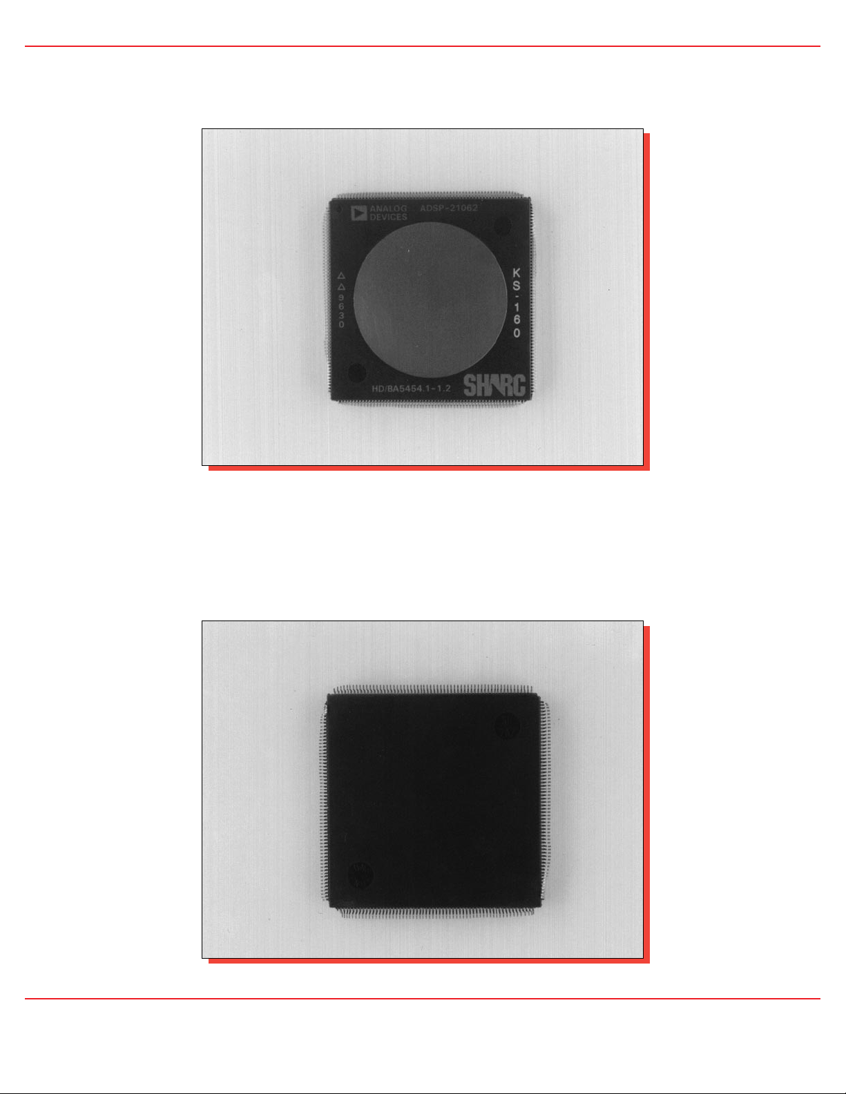
Figure 1. Package photographs of the Analog Devices ADSP-21062-KS-160
SHARC Digital Signal Processor. Mag. 1.5x.
Integrated Circuit Engineering CorporationAnalog Devices ADSP-21062-KS-160
Page 17
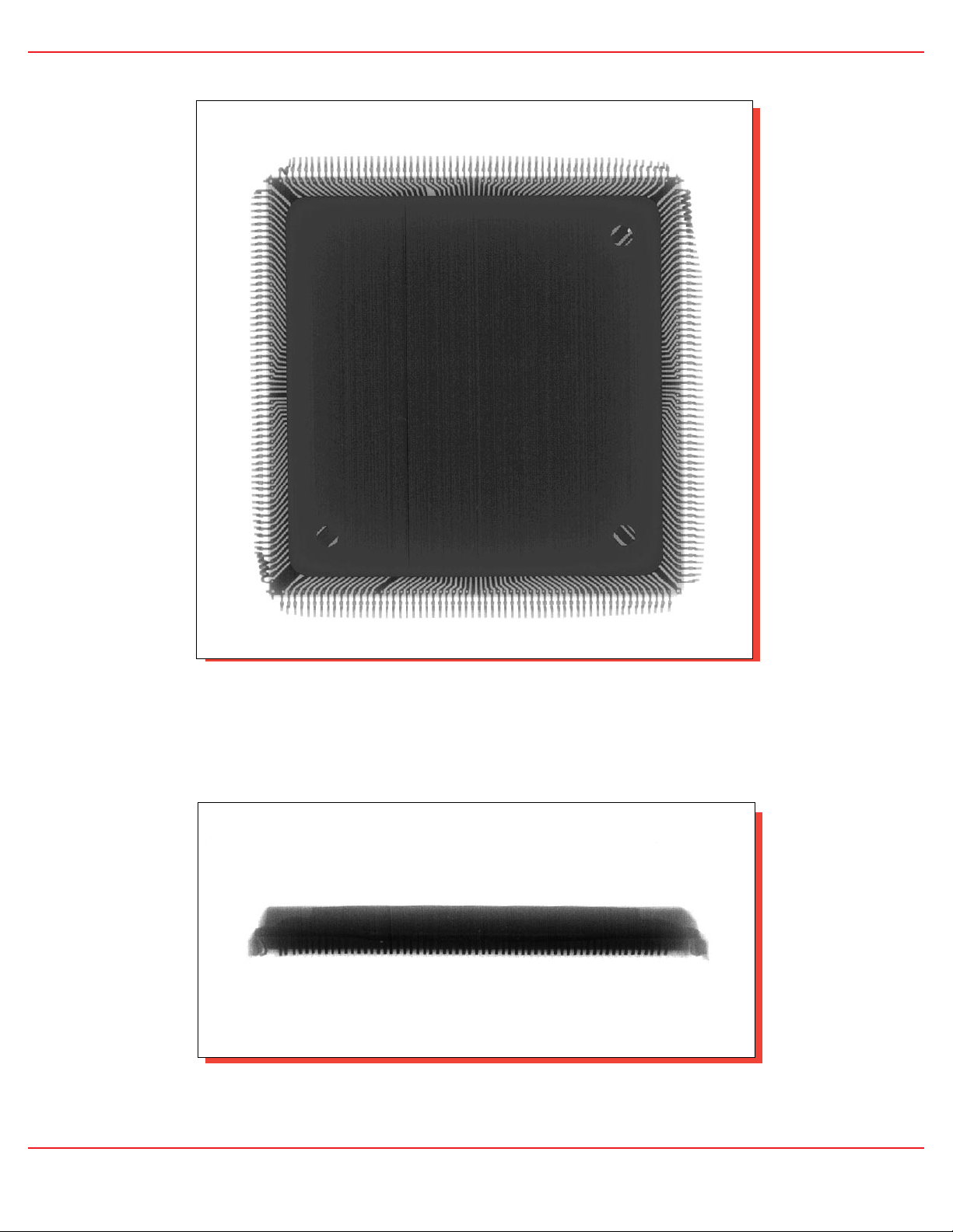
side
top
Figure 2. X-ray views of the package. Mag. 3x.
Integrated Circuit Engineering CorporationAnalog Devices ADSP-21062-KS-160
Page 18
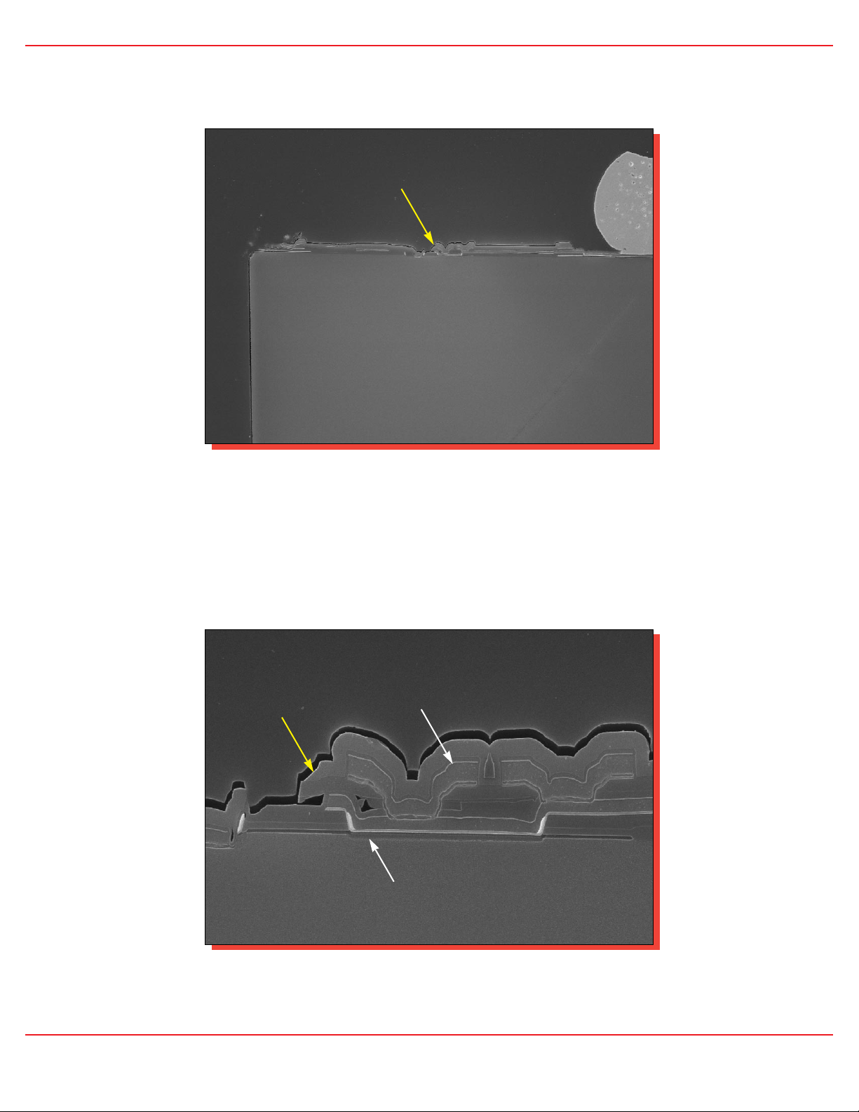
Mag. 6500x
Mag. 800x
Figure 3. SEM section views of the edge seal.
Integrated Circuit Engineering CorporationAnalog Devices ADSP-21062-KS-160
EDGE OF
PASSIVATION
EDGE OF
PASSIVATION
DIE
N+
METAL 1
METAL 2
Page 19

Integrated Circuit Engineering CorporationAnalog Devices ADSP-21062-KS-160
Figure 4. Portion of the Analog Devices ADSP-21062-KS-160 whole die. Mag. 26x.
Page 20

Integrated Circuit Engineering CorporationAnalog Devices ADSP-21062-KS-160
Figure 5. Portion of the Analog Devices ADSP-21062-KS-160 whole die. Mag. 26x.
Page 21

Integrated Circuit Engineering CorporationAnalog Devices ADSP-21062-KS-160
Figure 6. Portion of the Analog Devices ADSP-21062-KS-160 whole die. Mag. 26x.
Page 22

Integrated Circuit Engineering CorporationAnalog Devices ADSP-21062-KS-160
Figure 7. Remaining portion of the Analog Devices ADSP-21062-KS-160 whole die. Mag. 26x.
PIN 1
Page 23

Figure 8. Optical views of die markings. Mag. 750x.
Integrated Circuit Engineering CorporationAnalog Devices ADSP-21062-KS-160
Page 24

Figure 9. Optical views of die corners. Mag. 80x.
Integrated Circuit Engineering CorporationAnalog Devices ADSP-21062-KS-160
Page 25

Figure 10. Optical views illustrating a slotted bus line and resolution patterns.
Mag. 410x.
Integrated Circuit Engineering CorporationAnalog Devices ADSP-21062-KS-160
SLOT
Page 26

glass etch
Figure 11. SEM section views illustrating general structure. Mag. 13,000x.
Integrated Circuit Engineering CorporationAnalog Devices ADSP-21062-KS-160
PASSIVATION 1
PASSIVATION 2
PASSIVATION 2
METAL 2
METAL 2
METAL 1
METAL 1
W PLUG
W PLUG
N+ S/D
POLY 1 GATE
POLY 1 GATE
LOCOS
LOCOS
Page 27

Mag. 15,000x
Mag. 4600x
Figure 12. SEM views illustrating final passivation. 60°.
Integrated Circuit Engineering CorporationAnalog Devices ADSP-21062-KS-160
Page 28

Mag. 52,000x
Mag. 26,000x
Figure 13. SEM section views illustrating metal 2 line profiles.
Integrated Circuit Engineering CorporationAnalog Devices ADSP-21062-KS-160
PASSIVATION 2
PASSIVATION 1
INTERLEVEL DIELECTRIC
METAL 2
ALUMINUM 2
TIN CAP
TiN BARRIER
Page 29

Mag. 3200x
Mag. 6500x
Mag. 6500x
Integrated Circuit Engineering CorporationAnalog Devices ADSP-21062-KS-160
Figure 14. Topological SEM views of metal 2 patterning. 0°.
MASK
CHANGES
METAL 2
VIAS
Page 30

Mag. 10,000x
Mag. 10,000x
Mag. 20,000x
Integrated Circuit Engineering CorporationAnalog Devices ADSP-21062-KS-160
Figure 15. Perspective SEM views of metal 2 step coverage. 60°.
ALUMINUM 2
TiN CAP
Ti BARRIER
Page 31

Mag. 13,000x
Mag. 26,000x
Mag. 52,000x
Integrated Circuit Engineering CorporationAnalog Devices ADSP-21062-KS-160
Figure 16. SEM section views of typical vias.
PASSIVATION 2
METAL 2
METAL 2
METAL 2
INTERLEVEL
DIELECTRIC
METAL 1
METAL 1
METAL 1
90% THINNING
POLY 1
LOCOS
SOG
Page 32

Mag. 52,000x
Mag. 26,000x
Figure 17. SEM section views of metal 1 line profiles.
Integrated Circuit Engineering CorporationAnalog Devices ADSP-21062-KS-160
PASSIVATION
INTERLEVEL
DIELECTRIC
METAL 1
SOG
ALUMINUM 1
TiN CAP
TiN
BARRIER
Ti ADHESION LAYER
Page 33

Integrated Circuit Engineering CorporationAnalog Devices ADSP-21062-KS-160
Figure 18. Topological SEM views of metal 1 patterning. Mag. 6500x, 0°.
METAL 1
POLY 1
VIA
Page 34

Mag. 5000x
Mag. 10,000x
Mag. 20,000x
Integrated Circuit Engineering CorporationAnalog Devices ADSP-21062-KS-160
Figure 19. Perspective SEM views of metal 1 step coverage. 60°.
ALUMINUM 1
TiN CAP
TiN
BARRIER
Page 35

Mag. 32,000x
Mag. 16,000x
Figure 20. Perspective SEM views of metal 1 barrier and plug. 60°.
Integrated Circuit Engineering CorporationAnalog Devices ADSP-21062-KS-160
TiN
BARRIER
W PLUG
Page 36

Figure 21. SEM section views illustrating typical metal 1 contacts. Mag. 26,000x.
Integrated Circuit Engineering CorporationAnalog Devices ADSP-21062-KS-160
METAL 1
METAL 1
METAL 1
W PLUG
W PLUG
W PLUG
DEEP N+
N+
P+
POLY 1
LOCOS
LOCOS
Page 37

Mag. 3200x
Mag. 3200x
Mag. 5000x
Integrated Circuit Engineering CorporationAnalog Devices ADSP-21062-KS-160
Figure 22. Topological SEM views of poly 1 patterning. 0°.
P+
N+
POLY 1
Page 38

Mag. 8000x
Mag. 12,000x
Mag. 32,000x
Integrated Circuit Engineering CorporationAnalog Devices ADSP-21062-KS-160
Figure 23. Perspective SEM views of poly 1 coverage. 60°.
DIFFUSION
LOCOS
POLY 1 GATE
Page 39

N-channel
P-channel
glass etch
Integrated Circuit Engineering CorporationAnalog Devices ADSP-21062-KS-160
Figure 24. SEM section views of typical transistors. Mag. 52,000x.
W SILICIDE
POLY 1
POLY 1
GATE
POLY 1
GATE
GATE OXIDE
GATE OXIDE
P+ S/D
N+ S/D
DEEP N+ S/D
REFLOW GLASS
REFLOW GLASS
SIDEWALL
SPACER
Page 40

Figure 25. SEM section view of a typical birdsbeak. Mag. 52,000x.
Figure 26. Section views illustrating well structure.
Mag. 1200x
Mag. 6500x
Integrated Circuit Engineering CorporationAnalog Devices ADSP-21062-KS-160
DENSIFIED OXIDE
POLY 1
P-SUBSTRATE
P-WELL
P-WELL
N-WELL
LOCOS
LOCOS
METAL 2
P+
N+
GATE
OXIDE
Page 41

Mag. 1000x
Mag. 750x
Figure 27. Optical views of typical fuses.
Integrated Circuit Engineering CorporationAnalog Devices ADSP-21062-KS-160
BLOWN FUSE
Page 42

Mag. 3200x
Mag. 1600x
Figure 28. Topological SEM views of typical fuses. 0°.
Integrated Circuit Engineering CorporationAnalog Devices ADSP-21062-KS-160
INTACT
FUSE
LASER
BLOWN
FUSE
PASSIVATION
CUTOUT
Page 43

Mag. 4800x
Mag. 2400x
Figure 29. Perspective SEM views of typical fuses. 60°.
Integrated Circuit Engineering CorporationAnalog Devices ADSP-21062-KS-160
BLOWN FUSE
CUTOUT
PASSIVATION
Page 44

Mag. 6500x
Mag. 13,000x
Mag. 13,000x
Integrated Circuit Engineering CorporationAnalog Devices ADSP-21062-KS-160
Figure 30. SEM section views of a poly 1 fuse.
CUTOUT
CUTOUT
POLY 2
METAL 2
METAL 1
PASSIVATION 2
REFLOW GLASS
LOCOS
LOCOS
POLY 1
FUSE
POLY 1
FUSE
POLY 1 FUSE
Page 45

Figure 31. Color cross section drawing illustrating device structure.
Orange = Nitride, Blue = Metal, Yellow = Oxide, Green = Poly,
Red = Diffusion, and Gray = Substrate
Integrated Circuit Engineering CorporationAnalog Devices ADSP-21062-KS-160
,
,
,,
,,
POLY 1
W SILICIDE
INTERLEVEL DIELECTRIC
PRE-METAL GLASS
SOG
W PLUG
TiN CAP 1
TiN CAP 2
ALUMINUM 1
Ti BARRIER
TiN BARRIER 1
ALUMINUM 2
NITRIDE PASSIVATION
GLASS
PASSIVATION
GATE OXIDE
P SUBSTRATE
LOCAL OXIDE
DEEP N+
N+ S/D
P+ S/D
P-WELL
N-WELL
Ti ADHESION LAYER
,,,,,,,,,
,,,,,,,,,
Page 46

metal 2
metal 1
unlayered
Integrated Circuit Engineering CorporationAnalog Devices ADSP-21062-KS-160
Figure 32. Perspective SEM views of the SRAM cell array. Mag. 10,000x, 60°.
GND
GND
GND
BIT
BIT
BIT
BIT
WORD
“PIGGY BACK”
WORD LINE
Page 47

Integrated Circuit Engineering CorporationAnalog Devices ADSP-21062-KS-160
POLY 2
POLY 2
POLY 1
POLY 1
POLY 1
WORD LINE
Figure 33. Detailed SEM views of the SRAM cell structures (unlayered).
Mag. 42,000x, 60°.
Page 48

metal 2
metal 1
unlayered
Integrated Circuit Engineering CorporationAnalog Devices ADSP-21062-KS-160
Figure 34. Topological SEM views of the SRAM cell array. Mag. 3200x, 0°.
WORD LINE
“PIGGYBACK”
WORD LINE
GND
V
CC
GND
BIT
BIT
Page 49

metal 1
metal 2
Figure 35. Detailed topological SEM views of an SRAM cell. Mag. 13,000x, 0°.
Integrated Circuit Engineering CorporationAnalog Devices ADSP-21062-KS-160
GND
GND
BIT
BIT
BIT
BIT
“PIGGYBACK”
WORD LINE
V
CC
Page 50

unlayered
Figure 36. Detailed topological SEM view and schematic of an SRAM cell.
Mag. 13,000x, 0°.
Integrated Circuit Engineering CorporationAnalog Devices ADSP-21062-KS-160
BIT
R1
1
4
3
R2
2
BIT
GND
GND
V
CC
WORD
R2R1
BIT
1 2
3 4
BIT
Page 51

Mag. 13,000x
Mag. 20,000x
Mag. 26,000x
Integrated Circuit Engineering CorporationAnalog Devices ADSP-21062-KS-160
Figure 37. SEM section views of an SRAM cell (parallel to bit line).
METAL 2 BIT LINE
METAL 2 BIT LINE
METAL 1 LINK
METAL 1 LINK
SOG
POLY 2
W
PLUG
N+ S/D
N+ S/D
DEEP
N+ S/D
POLY 1
STORAGE
GATE
POLY 1
SELECT GATE
Page 52

Mag. 35,000x
Mag. 52,000x
Mag. 52,000x
Integrated Circuit Engineering CorporationAnalog Devices ADSP-21062-KS-160
Figure 38. SEM section views of SRAM cell details (parallel to bit line).
LOCOS
LOCOS
POLY 2
POLY 1
N+ S/D
N+ S/D
DEEP
N+ S/D
GATE OXIDE
GATE OXIDE
POLY 2 “PULL-UP”
RESISTOR
POLY 1 STORAGE
GATE
POLY 1 SELECT
GATE
Page 53

Mag. 26,000x
Mag. 13,000x
Figure 39. SEM section views of the SRAM cell array (perpendicular to bit lines).
Integrated Circuit Engineering CorporationAnalog Devices ADSP-21062-KS-160
LOCOS
GATE OXIDE
METAL 2
BIT LINE
BIT LINE
CONTACT
POLY 1
WORD/SELECT
LINE
POLY 1
WORD/SELECT
LINE
Page 54

Mag. 26,000x
Mag. 13,000x
Figure 40. SEM section views of the SRAM cell array (perpendicular to bit lines).
Integrated Circuit Engineering CorporationAnalog Devices ADSP-21062-KS-160
METAL
2
METAL 1 GND
N+ S/D
SOG
N+ S/D
POLY 1 STORAGE GATES
POLY 1 STORAGE GATE
POLY 2
LOCOS
Page 55

unlayered
intact
Figure 41. Optical views of typical device circuit layout. Mag. 820x.
Integrated Circuit Engineering CorporationAnalog Devices ADSP-21062-KS-160
Page 56

unlayered
intact
Figure 42. Optical views of typical I/O circuitry. Mag. 400x.
Integrated Circuit Engineering CorporationAnalog Devices ADSP-21062-KS-160
Page 57

Mag. 13,000x
Mag. 3200x
Figure 43. SEM section views illustrating wirebond interface.
Integrated Circuit Engineering CorporationAnalog Devices ADSP-21062-KS-160
Au
Au
EDGE OF PASSIVATION
METAL 1
METAL 2
POLY 1
LOCOS
METAL 1
Page 58

Mag. 26,000x
Mag. 13,000x
Figure 44. SEM section views of P-channel I/O circuitry.
Integrated Circuit Engineering CorporationAnalog Devices ADSP-21062-KS-160
METAL 2
METAL 1
METAL 1
P+ S/D
P+ S/D
POLY 1 GATE
POLY 1 GATE
SOG
SOG
Page 59

Mag. 26,000x
Mag. 13,000x
Figure 45. Additional SEM section views of N-channel I/O circuitry.
Integrated Circuit Engineering CorporationAnalog Devices ADSP-21062-KS-160
METAL 1
METAL 1
REFLOW GLASS
METAL 2
N+ S/D
N+ S/D
POLY 1 GATE
POLY 1 GATE
SOG
Page 60

P-channel
N-channel
Figure 46. SEM section views illustrating guardbands at the edge of the I/O circuitry.
Mag. 6500x.
Integrated Circuit Engineering CorporationAnalog Devices ADSP-21062-KS-160
METAL 2
N+ GUARDBAND
P+ GUARDBAND
P-WELL
N+ S/D
POLY 1 GATE
METAL 2
N+ GUARDBAND
P+ S/D
LOCOS
POLY 1 GATE
 Loading...