

Page 1

µ
PD78083
SUBSERIES
8-BIT SINGLE-CHIP MICROCONTROLLER
µ
PD78081
µ
PD78081(A)
µ
PD78082
µ
PD78P083µPD78P083(A)
Document No. U12176EJ2V0UM00 (2nd edition)
(O. D. No. IEU-886)
Date Published May 1997 N
1994
©
1992
Printed in Japan
µ
PD78082(A)
µ
PD78P081(A2)
Page 2

NOTES FOR CMOS DEVICES
1 PRECAUTION AGAINST ESD FOR SEMICONDUCTORS
Note:
Strong electric field, when exposed to a MOS device, can cause destruction of the gate oxide and
ultimately degrade the device operation. Steps must be taken to stop generation of static
electricity as much as possible, and quickly dissipate it once, when it has occurred. Environmental
control must be adequate. When it is dry, humidifier should be used. It is recommended to avoid
using insulators that easily build static electricity. Semiconductor devices must be stored and
transported in an anti-static container, static shielding bag or conductive material. All test and
measurement tools including work bench and floor should be grounded. The operator should be
grounded using wrist strap. Semiconductor devices must not be touched with bare hands. Similar
precautions need to be taken for PW boards with semiconductor devices on it.
2 HANDLING OF UNUSED INPUT PINS FOR CMOS
Note:
No connection for CMOS device inputs can be cause of malfunction. If no connection is provided
to the input pins, it is possible that an internal input level may be generated due to noise, etc., hence
causing malfunction. CMOS devices behave differently than Bipolar or NMOS devices. Input
levels of CMOS devices must be fixed high or low by using a pull-up or pull-down circuitry. Each
unused pin should be connected to V
possibility of being an output pin. All handling related to the unused pins must be judged device
by device and related specifications governing the devices.
DD or GND with a resistor, if it is considered to have a
3 STATUS BEFORE INITIALIZATION OF MOS DEVICES
Note:
Power-on does not necessarily define initial status of MOS device. Production process of MOS
does not define the initial operation status of the device. Immediately after the power source is
turned ON, the devices with reset function have not yet been initialized. Hence, power-on does
not guarantee out-pin levels, I/O settings or contents of registers. Device is not initialized until
the reset signal is received. Reset operation must be executed immediately after power-on for
devices having reset function.
Page 3

FIP, IEBus, and QTOP are trademarks of NEC Corporation.
MS-DOS and Windows are either registered trademarks or trademarks of Microsoft Corporation in the
United States and/or other countries.
IBM DOS, PC/AT and PC DOS are trademarks of International Business Machines Corporation.
HP9000 Series 300, HP9000 Series 700, and HP-UX are trademarks of Hewlett-Packard Company.
SPARCstation is a trademark of SPARC International, Inc.
Sun OS is a trademark of Sun Microsystems, Inc.
Ethernet is a trademark of XEROX Corporation.
NEWS and NEWS-OS are trademarks of SONY Corporation.
OSF/Motif is a trademark of Open Software Foundation, Inc.
TRON is an abbreviation of The Realtime Operating system Nucleus.
ITRON is an abbreviation of Industrial TRON.
The export of these products from Japan is regulated by the Japanese government. The export of some or all of these
products may be prohibited without governmental license. To export or re-export some or all of these products from a
country other than Japan may also be prohibited without a license from that country. Please call an NEC sales
representative.
License not needed:µPD78P083DU
The customer must judge the need for license:
µ
PD78081CU-×××, 78081GB-×××-3B4, 78081GB-×××-3BS-MTX
µ
PD78081GB(A)-×××-3B4, 78081GB(A2)-×××-3B4
µ
PD78082CU-×××, 78082GB-×××-3B4, 78082GB-×××-3BS-MTX
µ
PD78082GB(A)-×××-3B4
µ
PD78P083CU, 78P083GB-3B4, 78P083GB-3BS-MTX
µ
PD78P083CU(A), 78P083GB(A)-3B4, 78P083GB(A)-3BS-MTX
Page 4

The application circuits and their parameters are for reference only and are not intended for use in actual design-ins.
The information in this document is subject to change without notice.
No part of this document may be copied or reproduced in any form or by any means without the prior written
consent of NEC Corporation. NEC Corporation assumes no responsibility for any errors which may appear in
this document.
NEC Corporation does not assume any liability for infringement of patents, copyrights or other intellectual property
rights of third parties by or arising from use of a device described herein or any other liability arising from use
of such device. No license, either express, implied or otherwise, is granted under any patents, copyrights or other
intellectual property rights of NEC Corporation or others.
While NEC Corporation has been making continuous effort to enhance the reliability of its semiconductor devices,
the possibility of defects cannot be eliminated entirely. To minimize risks of damage or injury to persons or
property arising from a defect in an NEC semiconductor device, customers must incorporate sufficient safety
measures in its design, such as redundancy, fire-containment, and anti-failure features.
NEC devices are classified into the following three quality grades:
"Standard", "Special", and "Specific". The Specific quality grade applies only to devices developed based on a
customer designated “quality assurance program“ for a specific application. The recommended applications of
a device depend on its quality grade, as indicated below. Customers must check the quality grade of each device
before using it in a particular application.
Standard: Computers, office equipment, communications equipment, test and measurement equipment,
audio and visual equipment, home electronic appliances, machine tools, personal electronic
equipment and industrial robots
Special: Transportation equipment (automobiles, trains, ships, etc.), traffic control systems, anti-disaster
systems, anti-crime systems, safety equipment and medical equipment (not specifically designed
for life support)
Specific: Aircrafts, aerospace equipment, submersible repeaters, nuclear reactor control systems, life
support systems or medical equipment for life support, etc.
The quality grade of NEC devices is "Standard" unless otherwise specified in NEC's Data Sheets or Data Books.
If customers intend to use NEC devices for applications other than those specified for Standard quality grade,
they should contact an NEC sales representative in advance.
Anti-radioactive design is not implemented in this product.
M7 96.5
Page 5

Regional Information
Some information contained in this document may vary from country to country. Before using any NEC
product in your application, please contact the NEC office in your country to obtain a list of authorized
representatives and distributors. They will verify:
• Device availability
• Ordering information
• Product release schedule
• Availability of related technical literature
• Development environment specifications (for example, specifications for third-party tools and
components, host computers, power plugs, AC supply voltages, and so forth)
• Network requirements
In addition, trademarks, registered trademarks, export restrictions, and other legal issues may also vary
from country to country.
NEC Electronics Inc. (U.S.)
Santa Clara, California
Tel: 800-366-9782
Fax: 800-729-9288
NEC Electronics (Germany) GmbH
Duesseldorf, Germany
Tel: 0211-65 03 02
Fax: 0211-65 03 490
NEC Electronics (UK) Ltd.
Milton Keynes, UK
Tel: 01908-691-133
Fax: 01908-670-290
NEC Electronics Italiana s.r.1.
Milano, Italy
Tel: 02-66 75 41
Fax: 02-66 75 42 99
NEC Electronics (Germany) GmbH
Benelux Office
Eindhoven, The Netherlands
Tel:040-2445845
Fax: 040-2444580
NEC Electronics (France) S.A.
Velizy-Villacoublay, France
Tel:01-30-67 58 00
Fax: 01-30-67 58 99
NEC Electronics (France) S.A.
Spain Office
Madrid, Spain
Tel: 01-504-2787
Fax: 01-504-2860
NEC Electronics (Germany) GmbH
Scandinavia Office
Taeby, Sweden
Tel: 08-63 80 820
Fax: 08-63 80 388
NEC Electronics Hong Kong Ltd.
Hong Kong
Tel:2886-9318
Fax: 2886-9022/9044
NEC Electronics Hong Kong Ltd.
Seoul Branch
Seoul, Korea
Tel: 02-528-0303
Fax: 02-528-4411
NEC Electronics Singapore Pte. Ltd.
United Square, Singapore 1130
Tel:253-8311
Fax: 250-3583
NEC Electronics Taiwan Ltd.
Taipei, Taiwan
Tel: 02-719-2377
Fax: 02-719-5951
NEC do Brasil S.A.
Sao Paulo-SP, Brasil
Tel: 011-889-1680
Fax: 011-889-1689
J96. 8
Page 6

Major Revision in This Edition
Page Description
Throughout The following products have been already developed
µ
PD78081CU-×××, 78081GB-×××-3B4, 78082CU-×××, 78082GB-×××-3B4, 78P083CU, 78P083DU,
78P083GB-3B4
The following products have been added
µ
PD78081GB-×××-3BS-MTX, 78082GB-×××-3BS-MTX, 78P083GB-3BS-MTX, 78081GB(A)-×××-3B4,
78082GB(A)-×××-3B4, 78P083CU(A), 78P083GB(A)-3B4, 78P083GB(A)-3BS-MTX, 78081GB(A2)-×××-3B4
Changes supply voltage to VDD = 1.8 to 5.5V.
p. 9 1.6 78K/0 Series Development has been changed.
p. 13 1.9 Differences between the µPD78081, 78082, and 78P083, the µPD78081(A), 78082(A), and
78P083(A), and the µPD78081(A2) has been added.
p. 19 Cautions regarding the use of functions in common with 2.2.5 (2) (d) ASCK has been added.
p. 72 Cautions concerning the Write to OSMS Command has been added to 5.3 (2) Oscillation mode select
register (OSMS).
p. 73 Cautions concerning external clock input in 5.4.1 Main system clock oscillator has been changed.
p. 108 Figure 7-3. Watchdog Timer Mode Register Format, notes and cautions have been added.
p. 110 Description of 7.4.2 Interval timer operation has been changed.
p. 113 Cautions with regard to rewriting TCL0 to other than same data has been added to 8.3 (1) Timer clock
select register 0 (TCL0).
p. 120 The HSC bit has been added to the A/D Converter Mode
Register in Figure10-1. A/D Converter Block Diagram.
p. 122, 193 10.3 (1) A/D converter mode register (ADM), 13.1.1 Standby function, and Cautions have been added.
p. 137 Figure 11-1. Serial Interface Channel 2 Block Diagram has been corrected.
p. 146, 155 11.3 (4) (a), 11.4.2 (1) (d) (i) Generation of baud rate transmit/receive clock by means of main system
clock have been added.
76800 bps has been added to baud rate generated from the main system clock.
p. 161 Figure 11-10. Receive Error Timing has been corrected.
p. 165 11.4.3 (1) (c) Baud rate generator control register (BRGC) has been added.
p. 168 11.4.3 (3) MSB/LSB switching as start bit has been added.
p. 206 15.1 Memory Size Switching Register has been changed from W to R/W.
p. 205 Items and cautions have been added to Table 15-1. Differences between the µPD78P083 and Mask ROM
Versions.
p. 214 A description of the QTOP microcontroller has been added to 15.5 Screening of One-Time PROM
Versions.
p. 232 Figure A-1. Development Tool Configuration has been changed.
p. 231 APPENDIX A DEVELOPMENT TOOLS
The following Development Tools have been added:
IE-78000-R-A, IE-70000-98-IF-B, IE-70000-98N-IF, IE-70000-PC-IF-B, IE-78000-R-SV3, SM78K0, ID78K0
p. 239 A.4 OS for IBM PC has been added.
p. 240 Table A-2. System-Up Method from Other In-Circuit Emulator to IE-78000-R-A has been added.
p. 244 B.1 Real-time OS has been added.
p. 249 APPENDIX D REVISION HISTORY has been added.
The mark shows major revised points.
Page 7

PREFACE
Readers This manual has been prepared for user engineers who want to understand the
µ
functions of the
systems and programs.
µ
Caution In the
reliability required for use in customers’ mass-produced equipment.
Please use this device only for experimentation or for evaluation of functions.
Purpose This manual is intended for users to understand the functions described in the
Organization below.
Organization The
instruction edition (common to the 78K/0 Series).
PD78083 Subseries, the µPD78P083DU is not designed to maintain the
µ
PD78083 subseries manual is separated into two parts: this manual and the
µ
PD78083 Subseries 78K/0 Series
User’s Manual User’s Manual
(This Manual) Instruction
Pin functions CPU functions
Internal block functions Instruction set
Interrupt Explanation of each instruction
Other on-chip peripheral functions
PD78083 subseries and design and develop its application
How to Read This Manual Before reading this manual, you should have general knowledge of electric and logic
circuits and microcontrollers.
For those who will be using this as a manual for the µPD78081(A), 78082(A),
78P083(A) and 78081(A2):
µ
→ The
When you want to understand the functions in general:
→ Read this manual in the order of the contents.
To know the µPD78083 Subseries instruction function in detail:
→ Refer to the 78K/0 Series User's Manual: Instructions (IEU-1372)
How to interpret the register format:
→
To learn the function of a register whose register name is known:
→ Refer to Appendix C Register Index.
To know the electrical specifications of the µPD78083 Subseries:
→ Refer to separately available Data Sheet.
PD78081, 78082, 78P083 are explained as being representative de-
vices.
µ
In case this is used as a manual for the
or 78081(A2), please reread the product names as follows.
µ
PD78081 → µPD78081(A) or µPD78081(A2)
µ
PD78082 → µPD78082(A)
µ
PD78P083 → µPD78P083(A)
For the circled bit number, the bit name is defined as a reserved word in
RA78K/
0, and in CC78K/0, already defined in the header file named sfrbit.h.
PD78081(A), 78082(A), 78P083(A),
Page 8

To know application examples of the functions provided in the µPD78083 Subseries:
→ Refer to Application Note separately provided.
Legend Data representation weight : High digits on the left and low digits on the right
Active low representations : ××× (line over the pin and signal names)
Note : Description of note in the text.
Caution : Information requiring particular attention
Remarks : Additional explanatory material
Numeral representations : Binary ... ×××× or ××××B
Decimal ... ××××
Hexadecimal ... ××××H
Examples of use in this manual are prepared for “Standard” quality level devices for general electronic
equipment. In the case of examples of use in this manual for devices which meet “Special” quality level
requirements, please use each device only after studying each part that is actuall to be used, the circuitry
and the quality level of each component before use.
Page 9
Related Documents The related documents indicated in this publication may include preliminary
versions. However, preliminary versions are not marked as such.
Related documents for µPD78054 subseries
Document name
µ
PD78083 Subseries User’s Manual U12176J This Manual
µ
PD78081, 78082 Data Sheet U11415J U11415E
µ
PD78P083 Data Sheet U11006J U11006E
µ
PD78081(A), 78082(A), 78081(A2) Data Sheet In preparation
µ
PD78P083(A) Data Sheet U12175J U12175E
µ
PD78083 Subseries Special Function Register Table IEM-5599 —
78K/0 Series User’s Manual—Instruction IEU-849 IEU-1372
78K/0 Series Instruction Table U10903J —
78K/0 Series Instruction Set U10904J —
78K/0 Series Application Note Basics (III) IEA-767 U10182E
Document No.
Japanese English
To be prepared
Caution: The above documents are subject to change without prior notice. Be sure to use the latest version
document when starting design.
Page 10

Development Tool Documents (User’s Manuals)
Document name
RA78K Series Assembler Package Operation EEU-809 EEU-1399
Language EEU-815 EEU-1404
RA78K Series Structured Assembler Preprocessor EEU-817 EEU-1402
RA78K0 Assembler Package Structured assembly language U11789J U11789E
Assembly language U11801J U11801E
Operation U11802J U11802E
CC78K Series C Compiler Operation EEU-656 EEU-1280
Language EEU-655 EEU-1284
CC78K/0 C Compiler Operation U11517J U11517E
Language U11518J U11518E
CC78K/0 C Compiler Application Note Programming know-how EEA-618 EEA-1208
CC78K Series Library Source File EEU-777 —
PG-1500 PROM Programmer U11940J EEU-1335
PG-1500 Controller PC-9800 Series (MS-DOS™) Base EEU-704 EEU-1291
PG-1500 Controller IBM PC Series (PC DOS™) Base EEU-5008 U10540E
IE-78000-R EEU-810 U11376E
IE-78000-R-A U10057J U10057E
IE-78000-R-BK EEU-867 EEU-1427
IE-78078-R-EM U10775J U10775E
EP-78083 EEU-5003 EEU-1529
SM78K0 System Simulator Windows™ Base Reference U10181J U10181E
SM78K Series System Simulator External component user U10092J U10092E
open interface specifications
ID78K0 Integrated Debugger EWS Base Reference U11151J —
ID78K0 Integrated Debugger PC Base Reference U11539J —
ID78K0 Integrated Debugger Windows™ Base Guide U11649J U11649E
SD78K/0 Screen Debugger Introduction EEU-852 U10539E
PC-9800 Series (MS-DOS) Base Reference U10952J —
SD78K/0 Screen Debugger Introduction EEU-5024 EEU-1414
IBM PC/AT™ (PC DOS) Base Reference U11279J U11279E
Document No.
Japanese English
Caution: The above documents are subject to change without prior notice. Be sure to use the latest version
document when starting design.
Page 11
Documents for Embedded Software (User’s Manual)
Document name
78K/0 Series Real-Time OS Basics U11537J —
Installation U11536J —
Technicals U11538J —
OS for 78K/0 Series MX78K0 Basics EEU-5010 —
Fuzzy Knowledge Data Creation Tool EEU-829 EEU-1438
78K/0, 78K/II, 87AD Series Fuzzy Inference Development Support System—Translator EEU-862 EEU-1444
78K/0 Series Fuzzy Inference Development Support System—Fuzzy Inference Module EEU-858 EEU-1441
78K/0 Series Fuzzy Inference Development Support System—Fuzzy Inference Debugger EEU-921 EEU-1458
Document No.
Japanese English
Other Documents
Document name
IC PACKAGE MANUAL C10943X
Semiconductor Device Mounting Technology Manual C10535J C10535E
Quality Grade on NEC Semiconductor Devices C11531J C11531E
Reliability Quality Control on NEC Semiconductor Devices C10983J C10983E
Electric Static Discharge (ESD) Test MEM-539 —
Semiconductor Devices Quality Assurance Guide C11893J C11893E
Microcontroller Related Product Guide—Third Party Manufacturers U11416J —
Document No.
Japanese English
Caution: The above documents are subject to change without prior notice. Be sure to use the latest version
document when starting design.
Page 12

CONTENTS
CHAPTER 1 OUTLINE..................................................................................................................... 1
1.1 Features ............................................................................................................................. 1
1.2 Applications ...................................................................................................................... 2
1.3 Ordering Information ........................................................................................................ 2
1.4 Quality Grade .................................................................................................................... 3
1.5 Pin Configuration (Top View)........................................................................................... 4
1.6 78K/0 Series Development ............................................................................................... 9
1.7 Block Diagram................................................................................................................... 11
1.8 Outline of Function ........................................................................................................... 12
1.9 Differences between the µPD78081, 78082 and 78P083, the µPD78081(A), 78082(A)
and 78P083(A), and the µPD78081(A2) ........................................................................... 13
CHAPTER 2 PIN FUNCTION ...........................................................................................................15
2.1 Pin Function List ............................................................................................................... 15
2.1.1 Normal operating mode pins ............................................................................................... 15
µ
2.1.2 PROM programming mode pins (
PD78P083 only)............................................................ 16
2.2 Description of Pin Functions ........................................................................................... 17
2.2.1 P00 to P03 (Port 0) .............................................................................................................. 17
2.2.2 P10 to P17 (Port 1) .............................................................................................................. 17
2.2.3 P30 to P37 (Port 3) .............................................................................................................. 18
2.2.4 P50 to P57 (Port 5) .............................................................................................................. 18
2.2.5 P70 to P72 (Port 7) .............................................................................................................. 19
2.2.6 P100 to P101 (Port 10) ........................................................................................................ 19
2.2.7 AV
2.2.8 AV
2.2.9 AV
2.2.10 RESET................................................................................................................................. 20
2.2.11 X1 and X2 ............................................................................................................................ 20
2.2.12 V
2.2.13 V
2.2.14 V
2.2.15 IC (Mask ROM version only)................................................................................................21
2.2.16 NC (44-pin plastic QFP versions only)................................................................................. 21
REF .................................................................................................................................. 20
DD .................................................................................................................................... 20
SS .................................................................................................................................... 20
DD ...................................................................................................................................... 20
SS ...................................................................................................................................... 20
PP (
µ
PD78P083 only)......................................................................................................... 20
2.3 Pin Input/Output Circuits and Recommended Connection of Unused Pins ............... 22
CHAPTER 3 CPU ARCHITECTURE................................................................................................ 25
3.1 Memory Spaces................................................................................................................. 25
3.1.1 Internal program memory space.......................................................................................... 28
3.1.2 Internal data memory space ................................................................................................ 29
3.1.3 Special Function Register (SFR) area ................................................................................. 29
3.1.4 Data memory addressing .................................................................................................... 29
3.2 Processor Registers ......................................................................................................... 33
3.2.1 Control registers .................................................................................................................. 33
3.2.2 General registers ................................................................................................................. 36
– i –
Page 13

3.2.3 Special Function Register (SFR) ......................................................................................... 37
3.3 Instruction Address Addressing ..................................................................................... 40
3.3.1 Relative Addressing ............................................................................................................. 40
3.3.2 Immediate addressing ......................................................................................................... 41
3.3.3 Table indirect addressing..................................................................................................... 42
3.3.4 Register addressing............................................................................................................. 43
3.4 Operand Address Addressing ......................................................................................... 44
3.4.1 Implied addressing .............................................................................................................. 44
3.4.2 Register addressing............................................................................................................. 45
3.4.3 Direct addressing................................................................................................................. 46
3.4.4 Short direct addressing........................................................................................................ 47
3.4.5 Special-Function Register (SFR) addressing ...................................................................... 49
3.4.6 Register indirect addressing ................................................................................................ 50
3.4.7 Based addressing ................................................................................................................ 51
3.4.8 Based indexed addressing .................................................................................................. 52
3.4.9 Stack addressing ................................................................................................................. 52
CHAPTER 4 PORT FUNCTIONS .................................................................................................... 53
4.1 Port Functions................................................................................................................... 53
4.2 Port Configuration ............................................................................................................ 55
4.2.1 Port 0 ................................................................................................................................... 55
4.2.2 Port 1 ................................................................................................................................... 57
4.2.3 Port 3 ................................................................................................................................... 58
4.2.4 Port 5 ................................................................................................................................... 59
4.2.5 Port 7 ................................................................................................................................... 60
4.2.6 Port 10 ................................................................................................................................. 62
4.3 Port Function Control Registers ..................................................................................... 63
4.4 Port Function Operations................................................................................................. 67
4.4.1 Writing to input/output port................................................................................................... 67
4.4.2 Reading from input/output port ............................................................................................ 67
4.4.3 Operations on input/output port ........................................................................................... 67
CHAPTER 5 CLOCK GENERATOR................................................................................................ 69
5.1 Clock Generator Functions .............................................................................................. 69
5.2 Clock Generator Configuration ....................................................................................... 69
5.3 Clock Generator Control Register ................................................................................... 71
5.4 System Clock Oscillator................................................................................................... 73
5.4.1 Main system clock oscillator ................................................................................................ 73
5.4.2 Scaler................................................................................................................................... 75
5.5 Clock Generator Operations ............................................................................................ 76
5.6 Changing CPU Clock Settings ......................................................................................... 77
5.6.1 Time required for CPU clock switchover.............................................................................. 77
5.6.2 CPU clock switching procedure ........................................................................................... 78
CHAPTER 6 8-BIT TIMER/EVENT COUNTERS 5 AND 6 .............................................................. 79
6.1 8-Bit Timer/Event Counters 5 and 6 Functions .............................................................. 80
6.2 8-Bit Timer/Event Counters 5 and 6 Configurations...................................................... 82
6.3 8-Bit Timer/Event Counters 5 and 6 Control Registers ................................................. 84
– ii –
Page 14

6.4 8-Bit Timer/Event Counters 5 and 6 Operations ............................................................ 90
6.4.1 Interval timer operations ...................................................................................................... 90
6.4.2 External event counter operation......................................................................................... 93
6.4.3 Square-wave output ............................................................................................................ 94
6.4.4 PWM output operations ....................................................................................................... 96
6.5 Cautions on 8-Bit Timer/Event Counters 5 and 6 .......................................................... 100
CHAPTER 7 WATCHDOG TIMER................................................................................................... 103
7.1 Watchdog Timer Functions.............................................................................................. 103
7.2 Watchdog Timer Configuration ....................................................................................... 105
7.3 Watchdog Timer Control Registers................................................................................. 106
7.4 Watchdog Timer Operations ............................................................................................ 109
7.4.1 Watchdog timer operation.................................................................................................... 109
7.4.2 Interval timer operation ........................................................................................................ 110
CHAPTER 8 CLOCK OUTPUT CONTROL CIRCUIT ..................................................................... 1 11
8.1 Clock Output Control Circuit Functions ......................................................................... 111
8.2 Clock Output Control Circuit Configuration................................................................... 112
8.3 Clock Output Function Control Registers ...................................................................... 113
CHAPTER 9 BUZZER OUTPUT CONTROL CIRCUIT .................................................................... 115
9.1 Buzzer Output Control Circuit Functions ....................................................................... 115
9.2 Buzzer Output Control Circuit Configuration................................................................. 115
9.3 Buzzer Output Function Control Registers .................................................................... 116
CHAPTER 10 A/D CONVERTER....................................................................................................... 119
10.1 A/D Converter Functions.................................................................................................. 119
10.2 A/D Converter Configuration ........................................................................................... 119
10.3 A/D Converter Control Registers..................................................................................... 122
10.4 A/D Converter Operations................................................................................................ 126
10.4.1 Basic operations of A/D converter ....................................................................................... 126
10.4.2 Input voltage and conversion results ................................................................................... 128
10.4.3 A/D converter operating mode............................................................................................. 129
10.5 A/D Converter Cautions ................................................................................................... 131
CHAPTER 11 SERIAL INTERFACE CHANNEL 2 ............................................................................ 135
11.1 Serial Interface Channel 2 Functions.............................................................................. 135
11.2 Serial Interface Channel 2 Configuration ....................................................................... 136
11.3 Serial Interface Channel 2 Control Registers................................................................. 140
11.4 Serial Interface Channel 2 Operation .............................................................................. 148
11.4.1 Operation stop mode ........................................................................................................... 148
11.4.2 Asynchronous serial interface (UART) mode ...................................................................... 150
11.4.3 3-wire serial I/O mode ......................................................................................................... 163
CHAPTER 12 INTERRUPT FUNCTION ............................................................................................ 171
12.1 Interrupt Function Types.................................................................................................. 171
12.2 Interrupt Sources and Configuration .............................................................................. 172
12.3 Interrupt Function Control Registers.............................................................................. 175
– iii –
Page 15

12.4 Interrupt Servicing Operations ........................................................................................ 181
12.4.1 Non-maskable interrupt request acknowledge operation .................................................... 181
12.4.2 Maskable interrupt request acknowledge operation ............................................................ 184
12.4.3 Software interrupt request acknowledge operation ............................................................. 187
12.4.4 Multiple interrupt servicing ................................................................................................... 187
12.4.5 Interrupt request reserve ..................................................................................................... 191
CHAPTER 13 STANDBY FUNCTION................................................................................................ 193
13.1 Standby Function and Configuration.............................................................................. 193
13.1.1 Standby function .................................................................................................................. 193
13.1.2 Standby function control register ......................................................................................... 194
13.2 Standby Function Operations.......................................................................................... 195
13.2.1 HALT mode.......................................................................................................................... 195
13.2.2 STOP mode ......................................................................................................................... 198
CHAPTER 14 RESET FUNCTION..................................................................................................... 201
14.1 Reset Function .................................................................................................................. 201
CHAPTER 15µPD78P083 ................................................................................................................. 205
15.1 Memory Size Switching Register..................................................................................... 206
15.2 PROM Programming......................................................................................................... 207
15.2.1 Operating modes ................................................................................................................. 207
15.2.2 PROM write procedure ........................................................................................................ 209
15.2.3 PROM reading procedure.................................................................................................... 213
15.3 Erasure Procedure (µPD78P083DU Only)....................................................................... 214
15.4 Opaque Film Masking the Window (µPD78P083DU Only)............................................. 214
15.5 Screening of One-Time PROM Versions......................................................................... 214
CHAPTER 16 INSTRUCTION SET .................................................................................................... 215
16.1 Legends Used in Operation List...................................................................................... 216
16.1.1 Operand identifiers and description methods ...................................................................... 216
16.1.2 Description of “operation” column........................................................................................ 217
16.1.3 Description of “flag operation” column ................................................................................. 217
16.2 Operation List.................................................................................................................... 218
16.3 Instructions Listed by Addressing Type......................................................................... 226
APPENDIX A DEVELOPMENT TOOLS............................................................................................ 231
A.1 Language Processing Software ...................................................................................... 233
A.2 PROM Programming Tools .............................................................................................. 234
A.2.1 Hardware ............................................................................................................................. 234
A.2.2 Software............................................................................................................................... 234
A.3 Debugging Tools............................................................................................................... 235
A.3.1 Hardware ............................................................................................................................. 235
A.3.2 Software (1/3) ...................................................................................................................... 236
A.3.2 Software (2/3) ...................................................................................................................... 237
A.3.2 Software (3/3) ...................................................................................................................... 238
A.4 OS for IBM PC ................................................................................................................... 239
– iv –
Page 16

A.5 System-Upgrade Method from Other In-Circuit Emulators to 78K/0 Series
In-Circuit Emulator............................................................................................................ 240
APPENDIX B EMBEDDED SOFTWARE .......................................................................................... 243
B.1 Real-time OS...................................................................................................................... 244
B.2 Fuzzy Inference Development Support System............................................................. 245
APPENDIX C REGISTER INDEX ...................................................................................................... 247
C.1 Register Index ..................................................................................................................... 247
APPENDIX D REVISION HISTORY .................................................................................................. 249
– v –
Page 17

FIGURE (1/4)
Fig. No. Title Page
2-1 Pin Input/Output Circuit of List............................................................................................ 23
3-1 Memory Map (
3-2 Memory Map (
3-3 Memory Map (
3-4 Data Memory Addressing (
3-5 Data Memory Addressing (
3-6 Data Memory Addressing (
3-7 Program Counter Configuration ......................................................................................... 33
3-8 Program Status Word Configuration................................................................................... 33
3-9 Stack Pointer Configuration................................................................................................ 35
3-10 Data to be Saved to Stack Memory.................................................................................... 35
3-11 Data to be Reset from Stack Memory ................................................................................ 35
3-12 General Register Configuration .......................................................................................... 36
4-1 Port Types .......................................................................................................................... 53
4-2 P00 Block Diagram............................................................................................................. 56
4-3 P01 to P03 Block Diagram ................................................................................................. 56
4-4 P10 to P17 Block Diagram ................................................................................................. 57
4-5 P30 to P37 Block Diagram ................................................................................................. 58
4-6 P50 to P57 Block Diagram ................................................................................................. 59
4-7 P70 Block Diagram............................................................................................................. 60
4-8 P71 and P72 Block Diagram .............................................................................................. 61
4-9 P100 to P101 Block Diagram ............................................................................................. 62
4-10 Port Mode Register Format ................................................................................................ 65
4-11 Pull-Up Resistor Option Register Format ........................................................................... 66
µ
PD78081) .................................................................................................. 25
µ
PD78082) .................................................................................................. 26
µ
PD78P083)................................................................................................ 27
µ
PD78081)............................................................................... 30
µ
PD78082)............................................................................... 31
µ
PD78P083) ............................................................................ 32
5-1 Block Diagram of Clock Generator..................................................................................... 70
5-2 Processor Clock Control Register Format.......................................................................... 71
5-3 Oscillation Mode Selection Register Format ...................................................................... 72
5-4 Main System Clock Waveform due to Writing to OSMS.....................................................
5-5 External Circuit of Main System Clock Oscillator ............................................................... 73
5-6 Examples of Oscillator with Bad Connection (1/2) ............................................................. 74
5-7 CPU Clock Switching ......................................................................................................... 78
6-1 8-Bit Timer/Event Counters 5 and 6 Block Diagram ........................................................... 82
6-2 Block Diagram of 8-Bit Timer/Event Counters 5 and 6 Output Control Circuit ................... 83
6-3 Timer Clock Select Register 5 Format................................................................................ 85
6-4 Timer Clock Select Register 6 Format................................................................................ 86
6-5 8-Bit Timer Mode Control Register 5 Format...................................................................... 87
6-6 8-Bit Timer Mode Control Register 6 Format...................................................................... 88
6-7 Port Mode Register 10 Format ........................................................................................... 89
6-8 8-Bit Timer Mode Control Register Settings for Interval Timer Operation .......................... 90
6-9 Interval Timer Operation Timings ....................................................................................... 91
– vi –
Page 18

FIGURE (2/4)
Fig. No. Title Page
6-10 8-Bit Timer Mode Control Register Setting for External Event Counter Operation............. 93
6-11 External Event Counter Operation Timings (with Rising Edge Specification) .................... 93
6-12 8-Bit Timer Mode Control Register Settings for Square-Wave Output Operation .............. 94
6-13 8-Bit Timer Mode Control Register Settings for PWM Output Operation ........................... 96
6-14 PWM Output Operation Timing (Active high setting).......................................................... 97
6-15 PWM Output Operation Timings (CRn0 = 00H, active high setting)................................... 97
6-16 PWM Output Operation Timings (CRn0 = FFH, active high setting) .................................. 98
6-17 PWM Output Operation Timings (CRn0 changing, active high setting).............................. 99
6-18 8-Bit Timer Registers 5 and 6 Start Timing......................................................................... 100
6-19 External Event Counter Operation Timing.......................................................................... 100
6-20 Timing after Compare Register Change during Timer Count Operation ............................ 101
7-1 Watchdog Timer Block Diagram ......................................................................................... 105
7-2 Timer Clock Select Register 2 Format................................................................................ 107
7-3 Watchdog Timer Mode Register Format............................................................................. 108
8-1 Remote Controlled Output Application Example ................................................................ 111
8-2 Clock Output Control Circuit Block Diagram....................................................................... 112
8-3 Timer Clock Select Register 0 Format................................................................................ 113
8-4 Port Mode Register 3 Format ............................................................................................. 114
9-1 Buzzer Output Control Circuit Block Diagram .................................................................... 115
9-2 Timer Clock Select Register 2 Format................................................................................ 117
9-3 Port Mode Register 3 Format ............................................................................................. 118
10-1 A/D Converter Block Diagram ............................................................................................ 120
10-2 A/D Converter Mode Register Format ................................................................................ 123
10-3 A/D Converter Input Select Register Format ...................................................................... 124
10-4 External Interrupt Mode Register 1 Format ........................................................................ 125
10-5 A/D Converter Basic Operation .......................................................................................... 127
10-6 Relations between Analog Input Voltage and A/D Conversion Result................................ 128
10-7 A/D Conversion by Hardware Start .................................................................................... 129
10-8 A/D Conversion by Software Start...................................................................................... 130
10-9 Example of Method of Reducing Current Dissipation in Standby Mode............................. 131
10-10 Analog Input Pin Disposition .............................................................................................. 132
10-11 A/D Conversion End Interrupt Request Generation ...........................................................
10-12 Handling of AVDD Pin......................................................................................................... 133
11-1 Serial Interface Channel 2 Block Diagram ......................................................................... 137
11-2 Baud Rate Generator Block Diagram ................................................................................. 138
11-3 Serial Operating Mode Register 2 Format.......................................................................... 140
11-4 Asynchronous Serial Interface Mode Register Format....................................................... 141
11-5 Asynchronous Serial Interface Status Register Format ..................................................... 143
11-6 Baud Rate Generator Control Register Format (1/2) ......................................................... 144
– vii –
Page 19

FIGURE (3/4)
Fig. No. Title Page
11-6 Baud Rate Generator Control Register Format (2/2) ......................................................... 145
11-7 Asynchronous Serial Interface Transmit/Receive Data Format.......................................... 157
11-8 Asynchronous Serial Interface Transmission Completion Interrupt Request Timing.......... 159
11-9 Asynchronous Serial Interface Reception Completion Interrupt Request Timing............... 160
11-10 Receive Error Timing.......................................................................................................... 161
11-11 State of the Receive Buffer Register (RXB) when Reception is Interrupted, and
Generation/Non Generation of an Interrupt Request (INTSR) ........................................... 162
11-12 3-Wire serial I/O Mode Timing............................................................................................ 168
11-13 Circuit of Switching in Transfer Bit Order ........................................................................... 169
12-1 Basic Configuration of Interrupt Function (1/2)................................................................... 173
12-1 Basic Configuration of Interrupt Function (2/2)................................................................... 174
12-2 Interrupt Request Flag Register Format ............................................................................. 176
12-3 Interrupt Mask Flag Register Format.................................................................................. 177
12-4 Priority Specify Flag Register Format................................................................................. 178
12-5 External Interrupt Mode Register 0 Format ........................................................................ 179
12-6 External Interrupt Mode Register 1 Format ........................................................................ 179
12-7 Program Status Word Configuration................................................................................... 180
12-8 Flowchart from Non-Maskable Interrupt Request Generation to Acknowledgment............ 182
12-9 Non-Maskable Interrupt Request Acknowledge Timing ...................................................... 182
12-10 Non-Maskable Interrupt Request Acknowledge Operation ................................................ 183
12-11 Interrupt Request Acknowledge Processing Algorithm ....................................................... 185
12-12 Interrupt Request Acknowledge Timing (Minimum Time) ................................................... 186
12-13 Interrupt Request Acknowledge Timing (Maximum Time) .................................................. 186
12-14 Example of Multiple Interrupt (1/2) ..................................................................................... 189
12-14 Example of Multiple Interrupt (2/2) ..................................................................................... 190
12-15 Interrupt Request Hold ....................................................................................................... 192
13-1 Oscillation Stabilization Time Select Register Format........................................................ 194
13-2 HALT Mode Clear upon Interrupt Generation ..................................................................... 196
13-3 HALT Mode Release by RESET Input ................................................................................ 197
13-4 STOP Mode Release by Interrupt Generation.................................................................... 199
13-5 Release by STOP Mode RESET Input............................................................................... 200
14-1 Block Diagram of Reset Function ....................................................................................... 201
14-2 Timing of Reset Input by RESET Input............................................................................... 202
14-3 Timing of Reset due to Watchdog Timer Overflow ............................................................. 202
14-4 Timing of Reset Input in STOP Mode by RESET Input ...................................................... 202
15-1 Memory Size Switching Register Format ........................................................................... 206
15-2 Page Program Mode Flowchart.......................................................................................... 209
15-3 Page Program Mode Timing............................................................................................... 210
15-4 Byte Program Mode Flowchart ........................................................................................... 211
15-5 Byte Program Mode Timing................................................................................................ 212
– viii –
Page 20

FIGURE (4/4)
Fig. No. Title Page
15-6 PROM Read Timing ........................................................................................................... 213
A-1 Development Tool Configuration ........................................................................................ 232
A-2 EV-9200G-44 Drawing (For Reference Only)..................................................................... 241
A-3 EV-9200G-44 Footprint (For Reference Only).................................................................... 242
– ix –
Page 21

TABLE (1/2)
Table. No. Title Page
1-1 Differences between the µPD78081, 78082 and 78P083, the µPD78081(A), 78082(A)
µ
and 78P083(A), and the
2-1 Type of Input/Output Circuit of Each Pin ............................................................................ 22
3-1 Vector Table ........................................................................................................................ 28
3-2 Special-Function Register List (1/2) .................................................................................. 38
3-2 Special-Function Register List (2/2) ................................................................................... 39
4-1 Port Functions .................................................................................................................... 54
4-2 Port Configuration .............................................................................................................. 55
4-3 Port Mode Register and Output Latch Settings when Using Dual-Fucntions..................... 64
5-1 Clock Generator Configuration........................................................................................... 69
5-2 Maximum Time Required for CPU Clock Switchover ......................................................... 77
6-1 Timer/Event Counter Types and Functions ........................................................................ 79
6-2 8-Bit Timer/Event Counters 5 and 6 Interval Times............................................................ 80
6-3 8-Bit Timer/Event Counters 5 and 6 Square-Wave Output Ranges ................................... 81
6-4 8-Bit Timer/Event Counters 5 and 6 Configurations ........................................................... 82
6-5 8-Bit Timer/Event Counters 5 and 6 Interval Times............................................................ 92
6-6 8-Bit Timer/Event Counters 5 and 6 Square-Wave Output Ranges ................................... 95
PD78081(A2) ............................................................................ 13
7-1 Watchdog Timer Overrun Detection Times ......................................................................... 103
7-2 Interval Times ..................................................................................................................... 104
7-3 Watchdog Timer Configuration ........................................................................................... 105
7-4 Watchdog Timer Overrun Detection Time .......................................................................... 109
7-5 Interval Timer Interval Time ................................................................................................ 110
8-1 Clock Output Control Circuit Configuration ........................................................................ 112
9-1 Buzzer Output Control Circuit Configuration ...................................................................... 115
10-1 A/D Converter Configuration .............................................................................................. 119
11-1 Serial Interface Channel 2 Configuration ........................................................................... 136
11-2 Serial Interface Channel 2 Operating Mode Settings ......................................................... 142
11-3 Relation between Main System Clock and Baud Rate ....................................................... 146
11-4 Relation between ASCK Pin Input Frequency and Baud Rate (When BRGC is set to 00H) 147
11-5 Relation between Main System Clock and Baud Rate ....................................................... 155
11-6 Relation between ASCK Pin Input Frequency and Baud Rate (When BRGC is set to 00H) 156
11-7 Receive Error Causes ........................................................................................................ 161
– x –
Page 22

TABLE (2/2)
Table. No. Title Page
12-1 Interrupt Source List ........................................................................................................... 172
12-2 Various Flags Corresponding to Interrupt Request Sources .............................................. 175
12-3 Times from Maskable Interrupt Request Generation to Interrupt Service .......................... 184
12-4 Interrupt Request Enabled for Multiple Interrupt during Interrupt Servicing ....................... 188
13-1 HALT Mode Operating Status ............................................................................................. 195
13-2 Operation after HALT Mode Release ................................................................................. 197
13-3 STOP Mode Operating Status............................................................................................ 198
13-4 Operation after STOP Mode Release................................................................................. 200
14-1 Hardware Status after Reset (1/2)...................................................................................... 203
14-1 Hardware Status after Reset (2/2)...................................................................................... 204
µ
15-1 Differences between the
15-2 Examples of Memory Size Switching Register Settings ..................................................... 206
15-3 PROM Programming Operating Modes ............................................................................. 207
PD78P083 and Mask ROM Versions ....................................... 205
16-1 Operand Identifiers and Description Methods .................................................................... 216
A-1 System-Up Method from Other In-Circuit Emulator to IE-78000-R .................................... 240
A-2 System-Up Method from Other In-Circuit Emulator to IE-78000-R-A................................. 240
– xi –
Page 23

[MEMO]
– xii –
Page 24
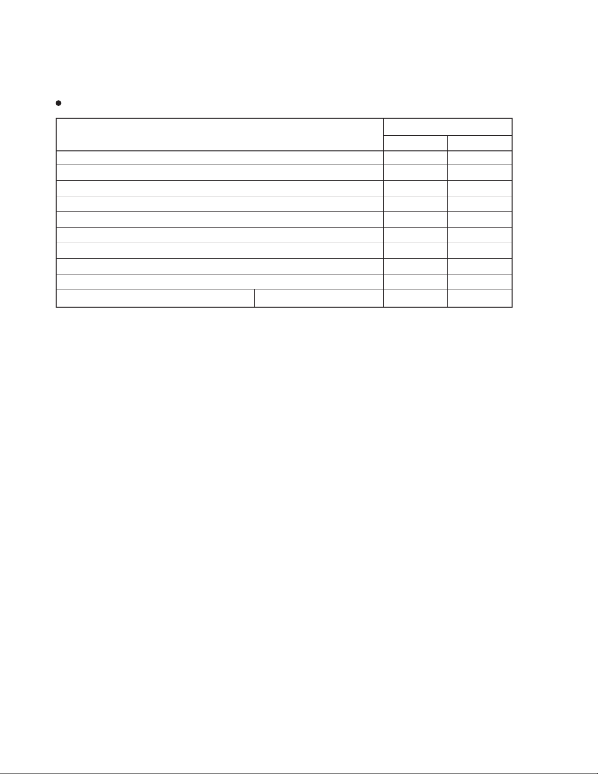
1.1 Features
On-chip ROM and RAM
CHAPTER 1 OUTLINE
CHAPTER 1 OUTLINE
Part Number
µ
PD78081
µ
PD78082
µ
PD78P083
Type
Program Memory
(ROM)
8 Kbytes
16 Kbytes
(
24 Kbytes
Note
)
Data Memory
(Internal High-Speed RAM)
256 bytes
384 bytes
512 bytes
(
Note
)
Note The capacities of internal PROM and internal high-speed RAM can be changed by means of the memory
size switching register (IMS).
Instruction execution time changeable from high speed (0.4 µs: In main system clock 5.0 MHz operation) to low
µ
speed (12.8
s: In main system clock 5.0 MHz operation)
Instruction set suited to system control
• Bit manipulation possible in all address spaces
• Multiply and divide instructions
33 I/O ports
8-bit resolution A/D converter: 8 channels
Serial interface: 1 channel
• 3-wire serial I/O/UART mode: 1 channel
Timer: 3 channels
• 8-bit timer/event counter : 2 channels
• Watchdog timer : 1 channel
Vectored Interrupt Source : 13
Supply voltage: VDD = 1.8 to 5.5 V
1
Page 25

CHAPTER 1 OUTLINE
1.2 Applications
µ
PD78081, 78082, 78P083:
Airbags, CRT displays, keyboards, air conditioners, hot water dispensers, boilers, fan heaters, dashboards, etc.
µ
PD78081(A), 78082(A), 78P083(A), 78081(A2):
Automobile electrical control devices, gas detector cutoff devices, various safety devices, etc.
1.3 Ordering Information
Part number Package Internal ROM
µ
PD78081CU-××× 42-pin plastic shrink DIP (600 mil) Mask ROM
µ
PD78081GB-×××-3B4 44-pin plastic QFP (10 × 10 mm) Mask ROM
µ
PD78081GB-×××-3BS-MTX 44-pin plastic QFP (10 × 10 mm) Mask ROM
µ
PD78082CU-××× 42-pin plastic shrink DIP (600 mil) Mask ROM
µ
PD78082GB-×××-3B4 44-pin plastic QFP (10 × 10 mm) Mask ROM
µ
PD78082GB-×××-3BS-MTX 44-pin plastic QFP (10 × 10 mm) Mask ROM
µ
PD78P083CU 42-pin plastic shrink DIP (600 mil) One-Time PROM
µ
PD78P083DU 42-pin ceramic shrink DIP (with window) (600 mil) EPROM
µ
PD78P083GB-3B4 44-pin plastic QFP (10 × 10 mm) One-Time PROM
µ
PD78P083GB-3BS-MTX 44-pin plastic QFP (10 × 10 mm) One-Time PROM
µ
PD78081GB(A)-×××-3B4 44-pin plastic QFP (10 × 10 mm) Mask ROM
µ
PD78082GB(A)-×××-3B4 44-pin plastic QFP (10 × 10 mm) Mask ROM
µ
PD78P083CU(A) 42-pin plastic shrink DIP (600 mil) One-Time PROM
µ
PD78P083GB(A)-3B4 44-pin plastic QFP (10 × 10 mm) One-Time PROM
µ
PD78P083GB(A)-3BS-MTX
µ
PD78081GB(A2)-×××-3B4 44-pin plastic QFP (10 × 10 mm) Mask ROM
Note
44-pin plastic QFP (10 × 10 mm) One-Time PROM
Note Under development
Remark ××× indicates ROM code suffix.
2
Page 26

CHAPTER 1 OUTLINE
1.4 Quality Grade
Part number Package Quality grade
µ
PD78081CU-××× 42-pin plastic shrink DIP (600 mil) Standard
µ
PD78081GB-×××-3B4 44-pin plastic QFP (10 × 10 mm) Standard
µ
PD78081GB-×××-3BS-MTX 44-pin plastic QFP (10 × 10 mm) Standard
µ
PD78082CU-××× 42-pin plastic shrink DIP (600 mil) Standard
µ
PD78082GB-×××-3B4 44-pin plastic QFP (10 × 10 mm) Standard
µ
PD78082GB-×××-3BS-MTX 44-pin plastic QFP (10 × 10 mm) Standard
µ
PD78P083CU 42-pin plastic shrink DIP (600 mil) Standard
µ
PD78P083DU 42-pin ceramic shrink DIP (with window) (600 mil) Not applicable
µ
PD78P083GB-3B4 44-pin plastic QFP (10 × 10 mm) Standard
µ
PD78P083GB-3BS-MTX 44-pin plastic QFP (10 × 10 mm) Standard
µ
PD78081GB(A)-×××-3B4 44-pin plastic QFP (10 × 10 mm) Special
µ
PD78082GB(A)-×××-3B4 44-pin plastic QFP (10 × 10 mm) Special
µ
PD78P083CU(A) 42-pin plastic shrink DIP (600 mil) Special
µ
PD78P083GB(A)-3B4 44-pin plastic QFP (10 × 10 mm) Special
µ
PD78P083GB(A)-3BS-MTX
µ
PD78081GB(A)-×××-3B4 44-pin plastic QFP (10 × 10 mm) Special
Note
44-pin plastic QFP (10 × 10 mm) Special
Note Under planning
Remark ××× indicates ROM code suffix.
Please refer to “Quality grade on NEC Semiconductor Devices” (Document number C11531E) published by
NEC Corporation to know the specification of quality grade on the devices and its recommended applications.
3
Page 27
1.5 Pin Configuration (Top View)
(1) Normal operating mode
42-pin plastic shrink DIP (600 mil)
µ
PD78081CU-×××, 78082CU-×××, 78P083CU, 78P083CU(A)
42-pin ceramic shrink DIP (with window) (600 mil)
µ
PD78P083DU
CHAPTER 1 OUTLINE
P55
P56
P57
P30
P31
P32
P33
P34
P35/PCL
P36/BUZ
P37
P00
P01/INTP1
P02/INTP2
P03/INTP3
RESET
IC (V
PP)
X2
X1
V
AVDD
1
2
3
4
5
6
7
8
9
10
11
12
13
14
15
16
17
18
19
DD
20
21
42
41
40
39
38
37
36
35
34
33
32
31
30
29
28
27
26
25
24
23
22
V
SS
P54
P53
P52
P51
P50
P100/TI5/TO5
P101/TI6/TO6
P70/R
XD/SI2
P71/T
XD/SO2
P72/ASCK/SCK2
P17/ANI7
P16/ANI6
P15/ANI5
P14/ANI4
P13/ANI3
P12/ANI2
P11/ANI1
P10/ANI0
AV
SS
AVREF
Cautions 1. Be sure to connect IC (Internally Connected) pin to VSS directly.
2. Connect AV
3. Connect AV
DD pin to VDD.
SS pin to VSS.
Remark Pin connection in parentheses is intended for the
4
µ
PD78P083.
Page 28
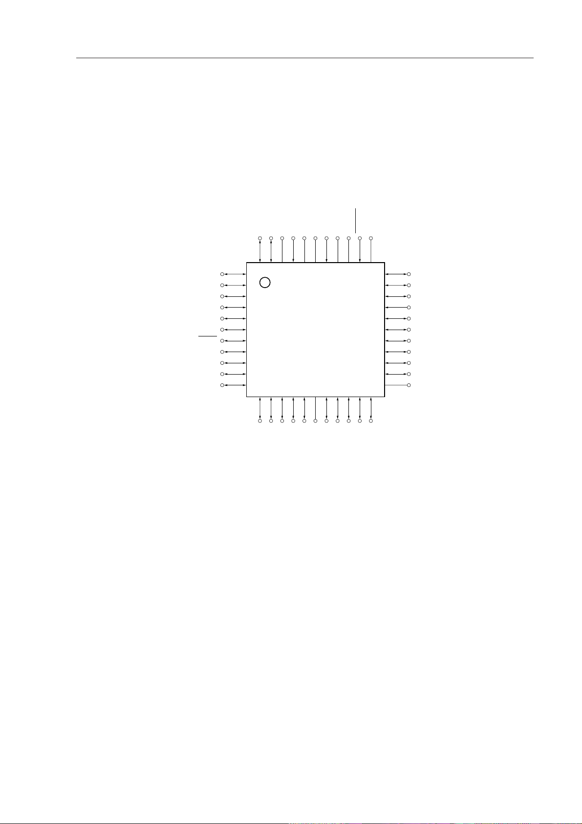
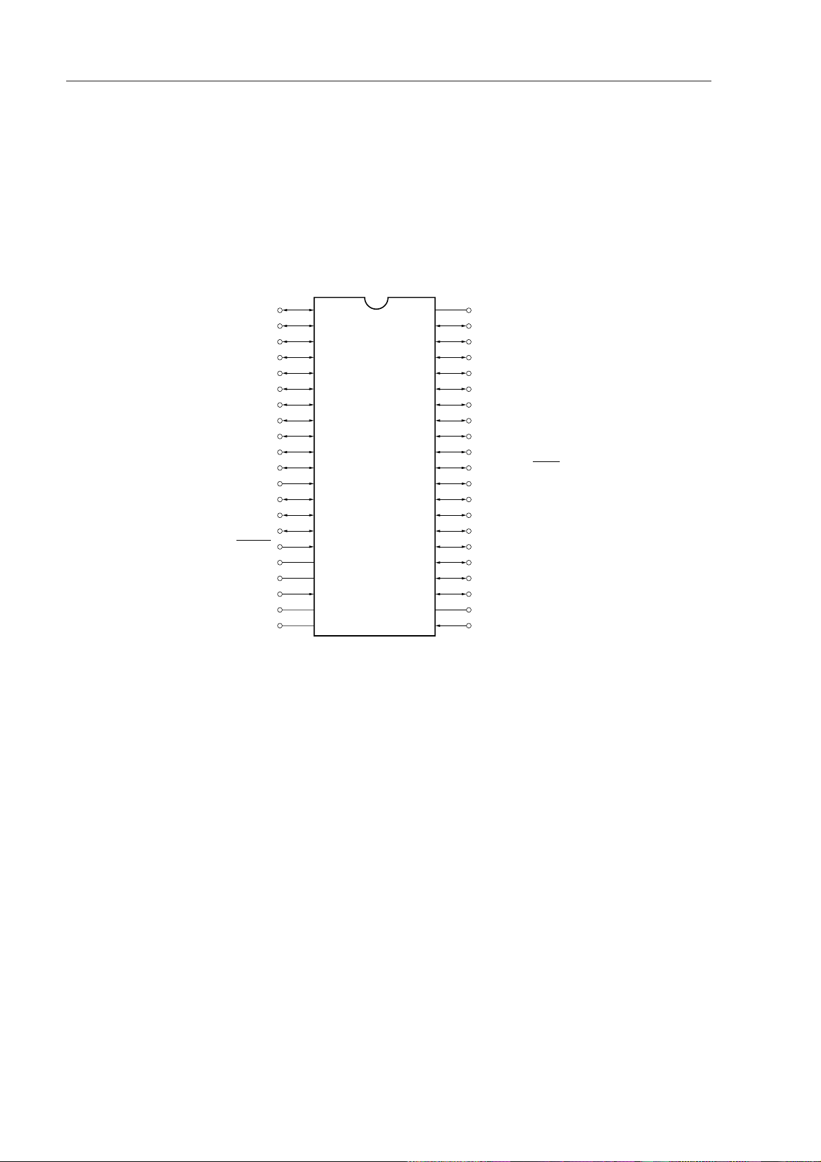
CHAPTER 1 OUTLINE
• 44-pin plastic QFP (10 × 10 mm)
µ
PD78081GB-×××-3B4, 78081GB-×××-3BS-MTX
µ
PD78082GB-×××-3B4, 78082GB-×××-3BS-MTX
µ
PD78P083GB-3B4, 78P083GB-3BS-MTX
µ
PD78081GB(A)-×××-3B4, 78082GB(A)-×××-3B4
µ
PD78P083GB(A)-3B4, 78P083GB(A)-3BS-MTX
µ
PD78P081GB(A2)-×××-3B4
P11/ANI1
P10/ANI0
AVSS
AVREF
Note
AVDD
VDDX1X2
IC (VPP)
RESET
NC
P12/ANI2
P13/ANI3
P14/ANI4
P15/ANI5
P16/ANI6
P17/ANI7
P72/ASCK/SCK2
P71/TxD/SO2
P70/RxD/SI2
P101/TI6/TO6
P100/TI5/TO6
44 43 42 41 40 39 38 37 36 35 34
1
2
3
4
5
6
7
8
9
10
11
12 13 14 15 16 17 18 19 20 21 22
VSS
P55
P56
P50
P51
P52
P53
P54
P57
P30
33
32
31
30
29
28
27
26
25
24
23
P31
Note Under development
Cautions 1. Be sure to connect IC (Internally Connected) pin to V
2. Connect AV
3. Connect AV
4. Connect NC pin to V
DD pin to VDD.
SS pin to VSS.
SS for noise protection (It can be left open).
P03/INTP3
P02/INTP2
P01/INTP1
P00
P37
P36/BUZ
P35/PCL
P34
P33
P32
NC
SS directly.
Remark Pin connection in parenthesis is intended for the
µ
PD78P083.
5
Page 29

CHAPTER 1 OUTLINE
Pin Identifications
ANI0 to ANI7 : Analog Input P100, P101 : Port 10
ASCK : Asynchronous Serial Clock PCL : Programmable Clock
DD : Analog Power Supply RESET : Reset
AV
REF : Analog Reference Voltage RxD : Receive Data
AV
SS : Analog Ground SCK2 : Serial Clock
AV
BUZ : Buzzer Clock SI2 : Serial Input
IC : Internally Connected SO2 : Serial Output
INTP1 to INTP3 : Interrupt from Peripherals TI5, TI6 : Timer Input
NC : Non-connection TO5 to TO6 : Timer Output
P00 to P03 : Port 0 TxD : Transmit Data
P10 to P17 : Port 1 V
P30 to P37 : Port 3 V
P50 to P57 : Port 5 V
P70 to P72 : Port 7 X1, X2 : Crystal (Main System Clock)
DD : Power Supply
PP : Programming Power Supply
SS : Ground
6
Page 30

CHAPTER 1 OUTLINE
(2) PROM programming mode
• 42-pin plastic shrink DIP (600 mil)
µ
PD78P083CU, 78P083CU(A)
• 42-pin ceramic shrink DIP (with window) (600 mil)
µ
PD78P083DU
A5
A6
A7
OE
CE
PGM
A8
1
2
3
4
5
6
7
8
(L)
9
10
11
A9
12
13
(L)
14
15
RESET
V
Open
(L)
V
VDD
PP
DD
16
17
18
19
20
21
Cautions 1. (L) : Individually connect to V
SS : Connect to the ground.
2. V
3. RESET: Set to the low level.
4. Open : Do not connect anything.
V
42
41
40
39
38
37
36
35
34
33
32
31
30
29
28
27
26
25
24
23
22
SS via a pull-down resistor.
SS
A4
A3
A2
A1
A0
A10
A11
A12
A13
A14
D7
D6
D5
D4
D3
D2
D1
D0
V
SS
VSS
7
Page 31

CHAPTER 1 OUTLINE
• 44-pin plastic QFP (10 × 10 mm)
µ
PD78P083GB-3B4, 78P083GB-3BS-MTX
µ
PD78P083GB(A)-3B4, 78P083GB(A)-3BS-MTX
Note
D2
D3
D4
D5
D6
D7
A14
A13
A12
A11
A10
D1D0VSS
44 43 42 41 40 39 38 37 36 35 34
1
2
3
4
5
6
7
8
9
10
11
12 13 14 15 16 17 18 19 20 21 22
A0A1A2A3A4
VSS
VDD
VDD
VSS
Note Under development
Cautions 1. (L) : Connect individually to V
SS : Connect to the ground.
2. V
3. RESET : Set to the low level.
4. Open : Do not connect anything.
(L)
Open
VPP
RESET
(L)
33
32
31
30
29
28
27
26
25
24
23
A5A6A7
SS via a pull-down resistor.
OE
CE
(L)
A9
(L)
A8
PGM
(L)
A0 to A14 : Address Bus RESET : Reset
CE : Chip Enable V
D0 to D7 : Data Bus V
OE : Output Enable V
DD : Power Supply
PP : Programming Power Supply
SS : Ground
PGM : Program
8
Page 32

CHAPTER 1 OUTLINE
100-pin
100-pin
100-pin
100-pin
80-pin
80-pin
80-pin
64-pin
64-pin
64-pin
64-pin
64-pin
64-pin
64-pin
42/44-pin
100-pin
100-pin
80-pin
80-pin
100-pin
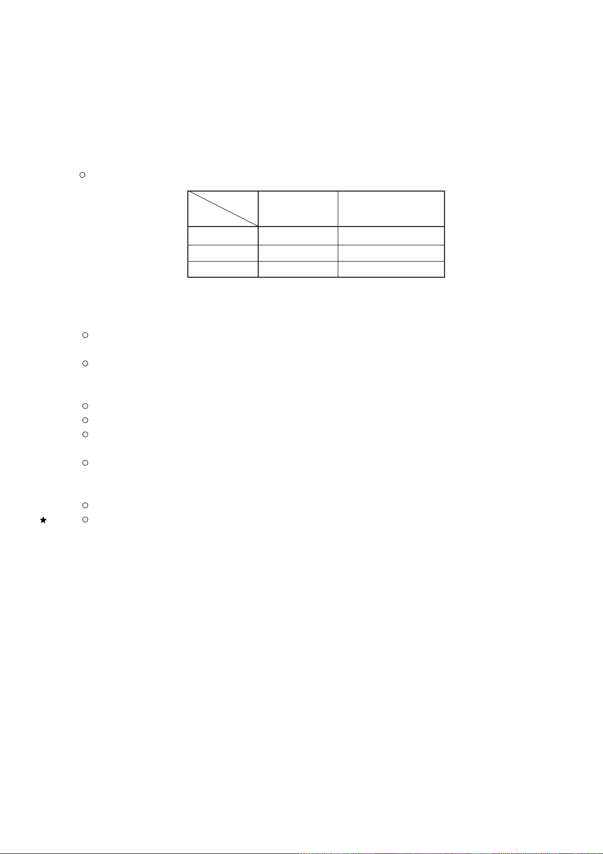
100-pin
100-pin
µPD780308Y
µPD78064Y
80-pin
78K/0
series
Control
FIP® driving
IEBus
TM
supported
Low EMI noise version of the µPD78078
Timer is added to the µPD78054 and its external interface is enhanced.
ROM-less versions of the µPD78078
Serial I/O of the µPD78078 is enhanced and only selected functions are provided.
Serial I/O-enhanced versions of the µPD78054; Low EMI noise version
Low EMI noise version of the µPD78054
UART and D/A converter are added to the µPD78014 and I/O is enhanced
.
A/D-enhanced version of the µPD780024
Serial I/O-enhanced versions of the µPD78018F; Low EMI noise version
Low EMI noise version of the µPD78018F
Low-voltage (1.8 V) operation versions of the µPD78014 with several ROM and RAM capacities available.
A/D converter and 16-bit timer are added to the µPD78002.
A/D converter is added to the µPD78002.
Basic subseries for control applications
On-chip UART, and operable at low voltage (1.8 V).
I/O and FIP C/D of the µPD78044F are enhanced. Total display outputs : 53 pins
I/O and FIP C/D of the µPD78044H are enhanced. Total display outputs : 48 pins
N-ch open-drain I/O is added to the µPD78044F. Total display outputs : 34 pins
Basic subseries for FIP driving. Total display outputs: 34 pins
SIO of the µPD78064 is enhanced, and ROM and RAM are expanded.
Low EMI noise version of the µPD78064
Basic subseries for driving LCDs and with on-chip UART.
IEBus controller is added to the µPD78054.
Mass-produced products
Products under development
Y Subseries supports the I
2
C bus specifications.
µPD78098
64-pin
LV
PWM output, LV digital code decoder and Hsync counter are incorporated.
µPD78P0914
µPD780308
64-pin
64-pin
Inverter control
A/D-enhanced version of the µPD780924
On-chip inverter control circuit and UART incorporated; Low EMI noise version
µPD780964
µPD780924
LCD driving
µPD78064B
µPD78064
µPD780208
µPD780228
µPD78044H
µPD78044F
µPD78075B
µPD78078
µPD78070A
µPD780018
Note
µPD780058
µPD78058F
µPD78054
µPD780034
µPD780024
µPD78014H
µPD78018F
µPD78014
µPD780001
µPD78002
µPD78083
µPD78075BY
µPD78078Y
µPD78070AY
µPD780018Y
Note
µPD780058Y
Note
µPD78058FY
µPD78054Y
µPD780034Y
µPD780024Y
µPD78018FY
µPD78014Y
µPD78002Y
1.6 78K/0 Series Development
The following shows the 78K/0 Series products development. Subseries names are shown inside frames.
Note Under planning
9
Page 33

CHAPTER 1 OUTLINE
The following table shows the differences among subseries functions.
Function ROM Timer 8-bit
Subseries name capacity 8-bit
Control
µ
PD78075B 32K to 40K 4 ch 1 ch 1 ch 1 ch 8 ch — 2 ch
µ
PD78078 48K to 60K
µ
PD78070A — 61 2.7 V
µ
PD780018 48K to 60K —
µ
PD780058 24K to 60K 2 ch 2 ch
µ
PD78058F 48K to 60K
µ
PD78054 16K to 60K 2.0 V
µ
PD780034 8K to 32K — 8 ch —
µ
PD780024 8 ch —
µ
PD78014H 2 ch 53
µ
PD78018F 8K to 60K
µ
PD78014 8K to 32K 2.7 V
µ
PD780001 8K — — 1 ch 39 —
16-bit Watch
WDT
A/D A/D D/A
10-bit
8-bit
Serial interface I/O
3 ch (UART: 1 ch)
2 ch (Time division
3-wire: 1 ch)
3 ch (Time division
UART: 1 ch)
3 ch (UART: 1 ch)
3 ch (UART: 1 ch, Time
division 3-wire: 1 ch)
VDD
MIN.
value
88 1.8 V Available
88
68 1.8 V
69 2.7 V
51 1.8 V
External
expansion
µ
PD78002 8K to 16K 1 ch — 53 Available
µ
PD78083 — 8 ch
µ
Inverter
control
FIP driving
LCD
driving
IEBus
supported
LV
PD780964 8K to 32K 3 ch Note —1 ch—8 ch—
µ
PD780924 8 ch —
µ
PD780208 32K to 60K 2 ch 1 ch 1 ch 1 ch 8 ch — — 2 ch 74 2.7 V —
µ
PD780228 48K to 60K 3 ch — — 1 ch 72 4.5 V
µ
PD78044H 32K to 48K 2 ch 1 ch 1 ch 68 2.7 V
µ
PD78044F 16K to 40K 2 ch
µ
PD780308 48K to 60K 2 ch 1 ch 1 ch 1 ch 8 ch — —
µ
PD78064B 32K
µ
PD78064 16K to 32K
µ
PD78098 32K to 60K 2 ch 1 ch 1 ch 1 ch 8 ch — 2 ch
µ
PD78P0914
32K 6 ch — — 1 ch 8 ch — — 2 ch 54 4.5 V Available
Note 10 bits timer: 1 channel
1 ch (UART: 1 ch)
2 ch (UART: 2 ch) 47 2.7 V
3 ch (Time division
UART: 1 ch)
2 ch (UART: 1 ch)
3 ch (UART: 1 ch)
33 1.8 V —
57 2.0 V —
69 2.7 V Available
Available
10
Page 34

1.7 Block Diagram
P100/TI5/TO5
P101/TI6/TO6
SI2/R
XD/P70
SO2/T
XD/P71
SCK2/ASCK/P72
ANI0/P10-
ANI7/P17
AV
DD
AVSS
AVREF
INTP1/P01-
INTP3/P03
BUZ/P36
PCL/P35
PORT 0
PORT 1
PORT 3
PORT 5
PORT 7
PORT 10
SYSTEM
CONTROL
8-bit TIMER/
EVENT COUNTER 5
BUZZER OUTPUT
INTERRUPT
CONTROL
A/D
CONVERTER
SERIAL
INTERFACE 2
WATCHDOG
TIMER
CLOCK OUTPUT
CONTROL
8-bit TIMER/
EVENT COUNTER 6
78K/0
CPU
CORE
ROM
RAM
P00
P01-P03
P10-P17
P30-P37
P50-P57
P70-P72
P100, P101
RESET
X1
X2
VDD VSS IC
(V
PP)
CHAPTER 1 OUTLINE
Remarks 1. The internal ROM and high-speed RAM capacities depend on the product.
µ
2. Pin connection in parentheses is intended for the
PD78P083.
11
Page 35

1.8 Outline of Function
CHAPTER 1 OUTLINE
Part Number
µ
PD78081
µ
PD78082
µ
PD78083
Item
Internal memory ROM Mask ROM PROM
8 Kbytes 16 Kbytes 24 Kbytes
High-speed RAM 256 bytes 384 bytes 512 bytes
Note
Note
Memory space 64 Kbytes
General register 8 bits × 32 registers (8 bits × 8 registers × 4 banks)
Instruction cycle Instruction execution time variable function is integrated.
0.4 µs/0.8 µs/1.6 µs/3.2 µ s/6.4 µs/12.8 µs (@5.0-MHz operation with main system clock)
Instruction set • 16-bit operation
• Multiply/divide (8 bits × 8 bits, 16 bits ÷ 8 bits)
• Bit manipulation (set, reset, test, Boolean operation)
• BCD adjust, etc.
I/O ports Total : 33
• CMOS input : 1
• CMOS input/output : 32
A/D converter • 8-bit resolution × 8 channels
Serial interface • 3-wire serial I/O/UART mode selectable: 1 channel
Timer • 8-bit timer/event counter: 2 channels
• Watchdog timer: 1 channel
Timer output 2 pins (8-bit PWM output enable)
Clock output 19.5 kHz, 39.1 kHz, 78.1 kHz, 156 kHz, 313 kHz, 625 kHz, 1.25 MHz, 2.5 MHz,
and 5.0 MHz (@ 5.0-MHz operation with main system clock)
Buzzer output 1.2 kHz, 2.4 kHz, 4.9 kHz, and 9.8 kHz
(@ 5.0-MHz operation with main system clock)
Vectored Maskable Internal : 8 external : 3
interrupt Non-maskable Internal : 1
source Software 1
Supply voltage V
Operating ambient temperature T
DD = 1.8 to 5.5 V
A = –40 to +85°C
Package • 42-pin plastic shrink DIP (600 mil)
• 44-pin plastic QFP (10 × 10 mm)
• 42-pin ceramic shrink DIP (with window) (600 mil) (
µ
PD78P083 only)
Note Internal PROM and high-speed RAM capacities can be changed by setting the internal memory size
switching register (IMS).
12
Page 36

CHAPTER 1 OUTLINE
1.9 Differences between the µPD78081, 78082 and 78P083, the µPD78081(A), 78082(A) and
78P083(A), and the µPD78081(A2)
Table 1-1 Differences between the µPD78081, 78082 and 78P083, the µPD78081(A), 78082(A) and
µ
78P083(A), and the
PD78081(A2)
Part Number
Item
Quality grade Standard Special
Supply voltage VDD = 1.8 to 5.5 V VDD = 4.5 to 5.5 V
Operating ambient temperature TA = –40 to +85°CTA = –40 to +125°C
Electrical specifications Please refer to the individual data sheets.
µ
PD78081
µ
PD78082
µ
PD78P083
µ
PD78081(A)
µ
PD78082(A)
µ
PD78P083(A)
µ
PD78081(A2)
13
Page 37

[MEMO]
CHAPTER 1 OUTLINE
14
Page 38
2.1 Pin Function List
2.1.1 Normal operating mode pins
(1) Port pins
CHAPTER 2 PIN FUNCTION
CHAPTER 2 PIN FUNCTION
Pin Name Input/Output Function After Reset
P00 Input Port 0 Input only Input —
P01 Input/output 4-bit input/output port Input/output is specifiable Input INTP1
P02 bit-wise. When used as the INTP2
P03 input port, it is possible to INTP3
connect a pull-up resistor by
software.
P10-P17 Input/output Port 1 Input ANI0-ANI7
8-bit input/output port
Input/output is specifiable bit-wise.
When used as the input port, it is possible to connect
a pull-up resistor by software.
P30-P34 Input/output Port 3 Input —
P35 8-bit input/output port PCL
P36 Input/output is specifiable bit-wise. BUZ
P37 When used as the input port, it is possible to connect —
a pull-up resistor by software.
P50-P57 Input/output Port 5 Input —
8-bit input/output port
A maximum of 7 out of 8 ports can drive LEDs directly.
Input/output is specifiable bit-wise.
When used as the input port, it is possible to connect
a pull-up resistor by software.
P70 Input/output Port 7 Input SI2/RxD
P71 3-bit input/output port SO2/TxD
P72 Input/output is specifiable bit-wise. SCK2/ASCK
When used as the input port, it is possible to connect
a pull-up resistor by software.
P100 Input/output Port 10 Input TI5/TO5
P101 2-bit input/output port TI6/TO6
Input/output is specifiable bit-wise.
When used as the input port, it is possible to connect
a pull-up resistor by software.
Note
Alternate Function
Note When P10/ANI0-P17/ANI7 pins are used as the analog inputs for the A/D converter, set the port 1 to
the input mode. The on-chip pull-up resistor is automatically disabled.
15
Page 39

CHAPTER 2 PIN FUNCTION
(2) Pins other than port pins
Pin Name Input/Output Function After Reset Alternate Function
INTP1 Input External interrupt request input by which the active edge Input P01
INTP2 (rising edge, falling edge, or both rising and falling edges) P02
INTP3 can be specified. P03
SI2 Input Serial interface serial data input. Input P70/RxD
SO2 Output Serial interface serial data output. Input P71/TxD
SCK2 Input/output Serial interface serial clock input/output. Input P72/ASCK
RxD Input Asynchronous serial interface serial data input. Input P70/SI2
TxD Output Asynchronous serial interface serial data output. Input P71/SO2
ASCK Input Asynchronous serial interface serial clock input. Input P72/SCK2
TI5 Input External count clock input to 8-bit timer (TM5). Input P100/TO5
TI6 External count clock input to 8-bit timer (TM6). P101/TO6
TO5 Output 8-bit timer output. (also used for 8-bit PWM output) Input P100/TI5
TO6 P101/TI6
PCL Output Clock output. (for main system clock trimming) Input P35
BUZ Output Buzzer output. Input P36
ANI0-ANI7 Input A/D converter analog input. Input P10-P17
AV
REF Input A/D converter reference voltage input. – –
AV
DD – A/D converter analog power supply. Connected to VDD.– –
AV
SS – A/D converter ground potential. Connected to VSS.– –
RESET Input System reset input. – –
X1 Input Main system clock oscillation crystal connection. – –
X2 – ––
V
DD – Positive power supply. – –
V
PP – High-voltage applied during program write/verification. – –
Connected directly to V
V
SS – Ground potential. – –
IC – Internal connection. Connect directly to V
NC – Does not internally connected. Connect to V
(It can be left open)
SS in normal operating mode.
SS.––
SS.––
2.1.2 PROM programming mode pins (µPD78P083 only)
Pin Name Input/Output Function
RESET Input PROM programming mode setting.
When +5 V or +12.5 V is applied to the VPP pin or a low level voltage is applied to the
RESET pin, the PROM programming mode is set.
VPP Input High-voltage application for PROM programming mode setting and program write/verify.
A0 to A14 Input Address bus
D0 to D7 Input/output Data bus
CE Input PROM enable input/program pulse input
OE Input Read strobe input to PROM
PGM Input Program/program inhibit input in PROM programming mode
VDD — Positive power supply
VSS — Ground potential
16
Page 40

CHAPTER 2 PIN FUNCTION
2.2 Description of Pin Functions
2.2.1 P00 to P03 (Port 0)
These are 4-bit input/output ports. Besides serving as input/output ports, they function as an external interrupt
request input.
The following operating modes can be specified bit-wise.
(1) Port mode
P00 functions as input-only port and P01 to P03 function as input/output ports.
P01 to P03 can be specified for input or output ports bit-wise with a port mode register 0 (PM0). When they
are used as input ports, on-chip pull-up resistors can be used to them by defining the pull-up resistor option
register L (PUOL).
(2) Control mode
INTP1 to INTP3 function as external interrupt request input pins which are capable of specifying the valid edges
(rising edge, falling edge, and both rising and falling edges).
2.2.2 P10 to P17 (Port 1)
These are 8-bit input/output ports. Besides serving as input/output ports, they function as an A/D converter analog
input.
The following operating modes can be specified bit-wise.
(1) Port mode
These ports function as 8-bit input/output ports.
They can be specified bit-wise as input or output ports with a port mode register 1 (PM1). If used as input
ports, on-chip pull-up resistors can be used to these ports by defining the pull-up resistor option register L
(PUOL).
(2) Control mode
These ports function as A/D converter analog input pins (ANI0-ANI7). The on-chip pull-up resistor is
automatically disabled when the pins specified for analog input.
17
Page 41

CHAPTER 2 PIN FUNCTION
2.2.3 P30 to P37 (Port 3)
These are 8-bit input/output ports. Beside serving as input/output ports, they function as clock output and buzzer
output.
The following operating modes can be specified bit-wise.
(1) Port mode
These ports function as 8-bit input/output ports. They can be specified bit-wise as input or output ports with
port mode register 3 (PM3). When they are used as input ports, on-chip pull-up resistors can be used by
defining the pull-up resistor option register L (PUOL).
(2) Control mode
These ports function as clock output, and buzzer output.
(a) PCL
Clock output pin.
(b) BUZ
Buzzer output pin.
2.2.4 P50 to P57 (Port 5)
These are 8-bit input/output ports. They can be specified bit-wise as input/output ports with port mode register
5 (PM5). When they are used as input ports, on-chip pull-up resistors can be used by defining the pull-up resistor
option register L (PUOL). A maximum of 7 out of 8 ports can drive LEDs directly.
18
Page 42

CHAPTER 2 PIN FUNCTION
2.2.5 P70 to P72 (Port 7)
This is a 3-bit input/output port. In addition to its use as an input/output port, it also has serial interface data input/
output and clock input/output functions.
The following operating modes can be specified bit-wise.
(1) Port mode
Port 7 functions as a 3-bit input/output port. Bit-wise specification as an input port or output port is possible
by means of port mode register 7 (PM7). When used as input ports, on-chip pull-up resistors can be used
by defining the pull-up resistor option register L (PUOL).
(2) Control mode
Port 7 functions as serial interface data input/output and clock input/output.
(a) SI2, SO2
Serial interface serial data input/output pins
(b) SCK2
Serial interface serial clock input/output pin.
(c) RxD, TxD
Asynchronous serial interface serial data input/output pins.
(d) ASCK
Asynchronous serial interface serial clock input pin.
Caution When this port is used as a serial interface, the I/O and output latches must be set according
to the function the user requires.
For the setting, see the operation mode setting list in Table 11-2 “Serial Interface Channel
2 Operating Mode Settings”
2.2.6 P100 to P101 (Port 10)
These are 2-bit input/output ports. Besides serving as input/output ports, they function as timer input/output.
The following operating modes can be specified bit-wise.
(1) Port mode
These ports function as 2-bit input/output ports. They can be specified bit-wise as input or output ports with
port mode register 10 (PM10). When they are used as input ports, on-chip pull-up resistors can be used by
defining the pull-up resistor option register H (PUOH).
(2) Control mode
These ports function as timer input/output.
(a) TI5, TI6
Pin for external clock input to the 8-bit timer/event counter 5 and 6.
(b) TO5, TO6
Timer output pins.
19
Page 43

CHAPTER 2 PIN FUNCTION
2.2.7 AVREF
A/D converter reference voltage input pin.
When A/D converter is not used, connect this pin to V
SS.
2.2.8 AV
DD
Analog power supply pin of A/D converter. Always use the same voltage as that of the VDD pin even when A/D
converter is not used.
2.2.9 AVSS
This is a ground voltage pin of A/D converter. Always use the same voltage as that of the VSS pin even when A/
D converter is not used.
2.2.10 RESET
This is a low-level active system reset input pin.
2.2.11 X1 and X2
Crystal resonator connect pins for main system clock oscillation. For external clock supply, input it to X1 and its
inverted signal to X2.
2.2.12 V
DD
Positive power supply pin
2.2.13 V
SS
Ground potential pin
2.2.14 V
PP (
µ
PD78P083 only)
High-voltage apply pin for PROM programming mode setting and program write/verify. Connect directly to V
in normal operating mode.
SS
20
Page 44

CHAPTER 2 PIN FUNCTION
2.2.15 IC (Mask ROM version only)
µ
The IC (Internally Connected) pin is provided to set the test mode to check the
Connect it directly to the V
When a voltage difference is produced between the IC pin and V
SS with the shortest possible wire in the normal operating mode.
SS pin because the wiring between those two pins
PD78083 Subseries at delivery.
is too long or an external noise is input to the IC pin, the user's program may not run normally.
Connect IC pins to VSS pins directly.
VSS IC
As short as possible
2.2.16 NC (44-pin plastic QFP versions only)
Not internally connected. Please connect to Vss (open is also possible)
21
Page 45

CHAPTER 2 PIN FUNCTION
2.3 Pin Input/Output Circuits and Recommended Connection of Unused Pins
Types of input/output circuits of the pins and recommeded connection of unused pins are shown in Table 2-1.
For the configuration of each type of input/output circuit, see Figure 2-1.
Table 2-1. Type of Input/Output Circuit of Each Pin
Pin Name Input/Output Input/Output Recommended Connection for Unused Pins
Circuit Type
P00 2 Input Connect to V
P01/INTP1 8-A Input/Output Independently connect to VSS via a resistor.
P02/INTP2
P03/INTP3
P10/ANI0-P17/ANI7 11 Input/Output Independently connect to V
P30-P32 5-A a resistor.
P33, P34 8-A
P35/PCL 5-A
P36/BUZ
P37
P50-P57 5-A
P70/SI2/RxD 8-A
P71/SO2/TxD 5-A
P72/SCK2/ASCK 8-A
P100/TI5/TO5 8-A
P101/TI6/TO6
RESET 2 Input –
AV
REF – – Connect to VSS.
AVDD Connect to VDD.
AV
SS Connect to V SS.
VPP (µPD78P083) Connect directly to VSS.
NC (44-pin plastic QFP Connect to V
version)
IC (Mask ROM version) Connect directly to V
SS.
DD or VSS via
SS (can also leave open)
SS.
22
Page 46

CHAPTER 2 PIN FUNCTION
Figure 2-1. Pin Input/Output Circuit of List
Type 2
IN
Type 5-A
pull-up
enable
data
output
disable
input
enable
Schmitt-Triggered Input with
Hysteresis Characteristics
VDD
VDD
P-ch
N-ch
P-ch
IN/OUT
Type 8-A
pull-up
enable
data
output
disable
Type 11
pull-up
enable
output
disable
comparator
input
enable
data
VDD
N-ch
P-ch
+
–
N-ch
V
REF (Threshold voltage)
P-ch
P-ch
N-ch
VDD
VDD
P-ch
V
P-ch
IN/OUT
DD
IN/OUT
23
Page 47

[MEMO]
CHAPTER 2 PIN FUNCTION
24
Page 48

3.1 Memory Spaces
Figures 3-1 to 3-3 shows memory maps.
CHAPTER 3 CPU ARCHITECTURE
CHAPTER 3 CPU ARCHITECTURE
Data memory
space
Program
memory
space
FFFFH
FF00H
FEFFH
FEE0H
FEDFH
FE00H
FDFFH
2000H
1FFFH
Figure 3-1. Memory Map (
Special Function
Registers (SFRs)
256 × 8 bits
General Registers
32 × 8 bits
Internal High-speed RAM
256 × 8 bits
Unusable
Internal ROM
8192 × 8 bits
µ
PD78081)
1FFFH
Program Area
1000H
0FFFH
CALLF Entry Area
0800H
07FFH
Program Area
0080H
007FH
CALLT Table Area
0040H
003FH
Vector Table Area
0000H
0000H
25
Page 49

CHAPTER 3 CPU ARCHITECTURE
Figure 3-2. Memory Map (µPD78082)
Data memory
space
Program
memory
space
FFFFH
FF00H
FEFFH
FEE0H
FEDFH
FD80H
FD7FH
4000H
3FFFH
Special Function
Registers (SFRs)
256 × 8 bits
General Registers
32 × 8 bits
Internal High-speed RAM
384 × 8 bits
Unusable
Internal ROM
16384 × 8 bits
3FFFH
Program Area
1000H
0FFFH
CALLF Entry Area
0800H
07FFH
Program Area
0080H
007FH
CALLT Table Area
0040H
003FH
Vector Table Area
0000H
0000H
26
Page 50

CHAPTER 3 CPU ARCHITECTURE
Figure 3-3. Memory Map (µPD78P083)
Data memory
space
Program
memory
space
FFFFH
FF00H
FEFFH
FEE0H
FEDFH
FD00H
FCFFH
6000H
5FFFH
Special Function
Registers (SFRs)
256 × 8 bits
General Registers
32 × 8 bits
Internal High-speed RAM
512 × 8 bits
Unusable
Internal PROM
24576 × 8 bits
5FFFH
Program Area
1000H
0FFFH
CALLF Entry Area
0800H
07FFH
Program Area
0080H
007FH
CALLT Table Area
0040H
003FH
Vector Table Area
0000H
0000H
27
Page 51

CHAPTER 3 CPU ARCHITECTURE
3.1.1 Internal program memory space
The internal program memory is mask ROM with a 8192 × 8-bit configuration in the
µ
8-bit configuration in the
The internal program memory space
PD78082, and PROM with a 24576 × 8-bit configuration in the µPD78P083.
stores programs and table data. Normally, they are addressed with a program
counter (PC).
The internal program memory is divided into the following three areas.
(1) Vector table area
The 64-byte area 0000H to 003FH is reserved as a vector table area. The RESET input and program start
addresses for branch upon generation of each interrupt request are stored in the vector table area. Of the
16-bit address, low-order 8 bits are stored at even addresses and high-order 8 bits are stored at odd addresses.
Table 3-1. Vector Table
Vector Table Address Interrupt Request
0000H RESET input
0004H INTWDT
0008H INTP1
000AH INTP2
000CH INTP3
0018H INTSER
001AH INTSR/INTCSI2
001CH INTST
0028H INTAD
002AH INTTM5
002CH INTTM6
003EH BRK
µ
PD78081, and a 16384 ×
(2) CALLT instruction table area
The 64-byte area 0040H to 007FH can store the subroutine entry address of a 1-byte call instruction (CALLT).
(3) CALLF instruction entry area
The area 0800H to 0FFFH can perform a direct subroutine call with a 2-byte call instruction (CALLF).
28
Page 52

CHAPTER 3 CPU ARCHITECTURE
3.1.2 Internal data memory space
µ
The internal high speed RAM configuration is 256 × 8-bit in the
µ
× 8-bit in the
are allocated in the 32-byte area FEE0H to FEFFH.
The internal high-speed RAM can also be used as a stack memory area.
3.1.3 Special Function Register (SFR) area
An on-chip peripheral hardware special-function register (SFR) is allocated in the area FF00H to FFFFH. (Refer
to Table 3-2. Special-Function Register List in 3.2.3 Special Function Register (SFR) ).
Caution Do not access addresses where the SFR is not assigned.
3.1.4 Data memory addressing
The method to specify the address of the instruction to be executed next, or the address of a register or memory
to be manipulated when an instruction is executed is called addressing.
The address of the instruction to be executed next is addressed by the program counter PC (for details, refer to
3.3 Instruction Address Addressing).
To address the memory that is manipulated when an instruction is executed, the
with many addressing modes with a high operability. Especially at addresses corresponding to data memory area,
particular addressing modes are possible to meet the functions of the special function registers (SFRs) and general
registers. This area is between FE00H and FFFFH for the
between FD00H and FFFFH for the
FFFFH). Figure 3-4 to 3-6 show the data memory addressing modes. For details of each addressing, refer to 3.4
Operand Address Addressing.
PD8P083. In this area, four banks of general registers, each bank consisting of eight 8-bit registers,
µ
µ
PD78P083. The data memory space is the entire 64K-byte space (0000H to
PD78081, 384 × 8-bit in the µPD78082 and 512
µ
PD78083 Subseries is provided
PD78081, FD80H and FFFFH for the µPD78082, and
29
Page 53
CHAPTER 3 CPU ARCHITECTURE
Figure 3-4. Data Memory Addressing (µPD78081)
FFFFH
FF20H
FF1FH
FF00H
FEFFH
FEE0H
FEDFH
FE20H
FE1FH
FE00H
FDFFH
2000H
1FFFH
0000H
Special Function
Registers (SFRs)
256 × 8 bits
General Registers
32 × 8 bits
Internal High-speed RAM
256 × 8 bits
Unusable
Internal ROM
8192 × 8 bits
SFR Addressing
Register Addressing
Short Direct
Addressing
Direct Addressing
Register Indirect
Addressing
Based Addressing
Based Indexed
Addressing
30
Page 54
CHAPTER 3 CPU ARCHITECTURE
Figure 3-5. Data Memory Addressing (µPD78082)
FFFFH
FF20H
FF1FH
FF00H
FEFFH
FEE0H
FEDFH
FE20H
FE1FH
FD80H
FD7FH
4000H
3FFFH
0000H
Special Function
Registers (SFRs)
256 × 8 bits
General Registers
32 × 8 bits
Internal High-speed RAM
384 × 8 bits
Unusable
Internal ROM
16384 × 8 bits
SFR Addressing
Register Addressing
Short Direct
Addressing
Direct Addressing
Register Indirect
Addressing
Based Addressing
Based Indexed
Addressing
31
Page 55

CHAPTER 3 CPU ARCHITECTURE
Figure 3-6. Data Memory Addressing (µPD78P083)
FFFFH
FF20H
FF1FH
FF00H
FEFFH
FEE0H
FEDFH
FE20H
FE1FH
FD00H
FCFFH
6000H
5FFFH
0000H
Special Function
Registers (SFRs)
256 × 8 bits
General Registers
32 × 8 bits
Internal High-speed RAM
512 × 8 bits
Unusable
Internal PROM
24576 × 8 bits
SFR Addressing
Register Addressing
Short Direct
Addressing
Direct Addressing
Register Indirect
Addressing
Based Addressing
Based Indexed
Addressing
32
Page 56

CHAPTER 3 CPU ARCHITECTURE
3.2 Processor Registers
The µPD78083 subseries units incorporate the following processor registers.
3.2.1 Control registers
The control registers control the program sequence, statuses and stack memory. The control registers consist
of a program counter, a program status word and a stack pointer.
(1) Program counter (PC)
The program counter is a 16-bit register which holds the address information of the next program to be
executed.
In normal operation, the PC is automatically incremented according to the number of bytes of the instruction
to be fetched. When a branch instruction is executed, immediate data and register contents are set.
RESET input sets the reset vector table values at addresses 0000H and 0001H to the program counter.
Figure 3-7. Program Counter Configuration
15 0
PC
(2) Program status word (PSW)
The program status word is an 8-bit register consisting of various flags to be set/reset by instruction execution.
Program status word contents are automatically stacked upon interrupt request generation or PUSH PSW
instruction execution and are automatically reset upon execution of the RETB, RETI and POP PSW
instructions.
RESET input sets the PSW to 02H.
Figure 3-8. Program Status Word Configuration
70
IE Z RBS1 AC RBS0 0 ISP CY
33
Page 57

CHAPTER 3 CPU ARCHITECTURE
(a) Interrupt enable flag (IE)
This flag controls the interrupt request acknowledge operations of the CPU.
When IE = 0, all interrupts except the non-maskable interrupt are disabled (DI status).
When IE = 1, interrupts are enabled (EI status). At this time, acknowledgment of interrupts is controlled
with an inservice priority flag (ISP), an interrupt mask flag for various interrupt sources, and a priority
specify flag.
The interrupt enable flag is reset to 0 when the DI instruction is executed or when an interrupt request
is acknowledged, and set to 1 when the EI instruction is executed.
(b) Zero flag (Z)
When the operation result is zero, this flag is set (1). It is reset (0) in all other cases.
(c) Register bank select flags (RBS0 and RBS1)
These are 2-bit flags to select one of the four register banks.
In these flags, the 2-bit information which indicates the register bank selected by SEL RBn instruction
execution is stored.
(d) Auxiliary carry flag (AC)
If the operation result has a carry from bit 3 or a borrow at bit 3, this flag is set (1). It is reset (0) in all
other cases.
(e) In-service priority flag (ISP)
This flag manages the priority of acknowledgeable maskable vectored interrupts. When ISP = 0, the
vectored interrupt request whose priority is specified by the priority specify flag registers (PR0L, PR0H,
and PR1L) (Refer to 12.3 (3) Priority specify flag registers (PR0L, PR0H, and PR1L)) to be low is
disabled. Whether the interrupt request is actually acknowledged is controlled by the status of the interrupt
enable flag (IE).
(f) Carry flag (CY)
This flag stores overflow and underflow upon add/subtract instruction execution. It stores the shift-out
value upon rotate instruction execution and functions as a bit accumulator during bit manipulation
instruction execution.
34
Page 58

CHAPTER 3 CPU ARCHITECTURE
(3) Stack pointer (SP)
This is a 16-bit register to hold the start address of the memory stack area. Only the internal high-speed RAM
µ
area (FE00H-FEFFH for the
µ
PD78P083) can be set as the stack area.
PD78081, FD80H-FEFFH for the µPD78082, and FD00H-FEFFH for the
Figure 3-9. Stack Pointer Configuration
015
SP
The SP is decremented ahead of write (save) to the stack memory and is incremented after read (reset) from
the stack memory.
Each stack operation saves/resets data as shown in Figures 3-10 and 3-11.
Caution Since RESET input makes SP contents indeterminate, be sure to initialize the SP before
instruction execution.
Figure 3-10. Data to be Saved to Stack Memory
SP SP _ 2
SP _ 2
SP _ 1
SP
SP
PUSH rp Instruction
Register Pair Lower
Register Pair Upper
Figure 3-11. Data to be Reset from Stack Memory
Register Pair Lower
SP SP _ 2
SP _ 2
SP _ 1
SP
SP
CALL, CALLF, and
CALLT Instruction
PC7-PC0
PC15-PC8
RET InstructionPOP rp Instruction
PC7-PC0
SP SP _ 3
SP _ 3
SP _ 2
SP _ 1
SP
SP
Interrupt and
BRK Instruction
PC7-PC0
PC15-PC8
PSW
RETI and RETB
Instruction
PC7-PC0
SP + 1
SP SP + 2
Register Pair Upper
SP + 1
SP SP + 2
PC15-PC8
SP + 1
SP + 2
SP SP + 3
PC15-PC8
PSW
35
Page 59

CHAPTER 3 CPU ARCHITECTURE
3.2.2 General registers
A general register is mapped at particular addresses (FEE0H to FEFFH) of the data memory. It consists of 4 banks,
each bank consisting of eight 8-bit registers (X, A, C, B, E, D, L and H).
Each register can also be used as an 8-bit register. Two 8-bit registers can be used in pairs as a 16-bit register
(AX, BC, DE and HL).
They can be described in terms of function names (X, A, C, B, E, D, L, H, AX, BC, DE and HL) and absolute names
(R0 to R7 and RP0 to RP3).
Register banks to be used for instruction execution are set with the CPU control instruction (SEL RBn). Because
of the 4-register bank configuration, an efficient program can be created by switching between a register for normal
processing and a register for interruption request for each bank.
Figure 3-12. General Register Configuration
(a) Absolute Name
16-Bit Processing 8-Bit Processing
FEFFH
FEF8H
FEF0H
FEE8H
FEE0H
BANK0
BANK1
BANK2
BANK3
RP3
RP2
RP1
RP0
15 0 7 0
R7
R6
R5
R4
R3
R2
R1
R0
FEFFH
FEF8H
FEF0H
FEE8H
FEE0H
36
BANK0
BANK1
BANK2
BANK3
(b) Function Name
16-Bit Processing 8-Bit Processing
H
HL
L
D
DE
E
B
BC
C
A
AX
X
15 0 7 0
Page 60

CHAPTER 3 CPU ARCHITECTURE
3.2.3 Special Function Register (SFR)
Unlike a general register, each special-function register has special functions.
It is allocated in the FF00H to FFFFH area.
The special-function register can be manipulated like the general register, with the operation, transfer and bit
manipulation instructions. Manipulatable bit units, 1, 8 and 16, depend on the special-function register type.
Each manipulation bit unit can be specified as follows.
• 1-bit manipulation
Describe the symbol reserved with assembler for the 1-bit manipulation instruction operand (sfr.bit).
This manipulation can also be specified with an address.
• 8-bit manipulation
Describe the symbol reserved with assembler for the 8-bit manipulation instruction operand (sfr).
This manipulation can also be specified with an address.
• 16-bit manipulation
Describe the symbol reserved with assembler for the 16-bit manipulation instruction operand (sfrp).
When addressing an address, describe an even address.
Table 3-2 gives a list of special-function registers. The meaning of items in the table is as follows.
• Symbol
Symbols indicating the addresses of special function register. These symbols are reserved words for the RA78K/
0 and defined by header file sfrbit.h for the CC78K/0, and can be used as the operands of instructions when
the RA78K/0, ID78K0, and SD78K/0 are used.
• R/W
Indicates whether the corresponding special-function register can be read or written.
R/W : Read/write enable
R : Read only
W : Write only
• Manipulatable bit units
√ indicates bit units (1, 8 or 16 bits) in which the register can be manipulated. — indicates that the register cannot
be manipulated in the indicated bit units.
• After reset
Indicates each register status upon RESET input.
37
Page 61

CHAPTER 3 CPU ARCHITECTURE
Table 3-2. Special-Function Register List (1/2)
Address Special-Function Register (SFR) Name Symbol R/W After Reset
FF00H Port0 P0 R/W √√— 00H
FF01H Port1 P1 √√—
FF03H Port3 P3 √√—
FF05H Port5 P5 √√—
FF07H Port7 P7 √√—
FF0AH Port10 P10 √√—
FF1FH A/D conversion result register ADCR R √√— Undefined
FF20H Port mode register 0 PM0 R/W √√— FFH
FF21H Port mode register 1 PM1 √√—
FF23H Port mode register 3 PM3 √√—
FF25H Port mode register 5 PM5 √√—
FF27H Port mode register 7 PM7 √√—
FF2AH Port mode register 10 PM10 √√—
FF40H Timer clock select register 0 TCL0 √√— 00H
FF42H Timer clock select register 2 TCL2 — √ —
FF50H Compare Register 50 CR50 — √ —
FF51H 8-bit timer register 5 TM5 R — √ —
FF52H Timer clock select register 5 TCL5 R/W — √ —
FF53H 8-bit timer mode control register 5 TMC5 √√—
FF54H Compare Register 60 CR60 — √ —
FF55H 8-bit timer register 6 TM6 R — √ —
FF56H Timer clock select register 6 TCL6 R/W — √ —
FF57H 8-bit timer mode control register 6 TMC6 √√—
FF70H
FF71H
FF72H Serial operating mode register 2 CSIM2 R/W √√—
FF73H Baud rate generator control register BRGC — √ —
FF74H Transmit shift register TXS SIO2 W — √ — FFH
FF80H A/D converter mode register ADM R/W √√— 01H
FF84H A/D converter input select register ADIS — √ — 00H
FFE0H Interrupt request flag register 0L IF0 IF0L √√ √
FFE1H Interrupt request flag register 0H IF0H √√
FFE2H Interrupt request flag register 1L IF1L √√—
FFE4H Interrupt mask flag register 0L MK0 MK0L √√ √FFH
FFE5H Interrupt mask flag register 0H MK0H √√
FFE6H Interrupt mask flag register 1L MK1L √√—
FFE8H Priority order specify flag register 0L PR0 PR0L √√ √
FFE9H Priority order specify flag register 0H PR0H √√
Asynchronous serial interface mode register
Asynchronous serial interface status register
Receive buffer register RXB R
ASIM √√—
ASIS R √√—
Manipulatable Bit Unit
8 bits1 bit 16 bits
38
Page 62

CHAPTER 3 CPU ARCHITECTURE
Table 3-2. Special-Function Register List (2/2)
Address Special-Function Register (SFR) Name Symbol R/W After Reset
FFEAH Priority order specify flag register 1L PR1L R/W √√— FFH
FFECH External interrupt mode register 0 INTM0 — √ — 00H
FFEDH External interrupt mode register 1 INTM1 — √ —
FFF0H Memory size switching register IMS — √ —
FFF2H Oscillation mode selection register OSMS W — √ — 00H
FFF3H Pull-up resistor option register H PUOH R/W √√—
FFF7H Pull-up resistor option register L PUOL √√—
FFF9H Watchdog timer mode register WDTM √√—
FFFAH
FFFBH Processor clock control register PCC √√—
Oscillation stabilization time select register
OSTS — √ — 04H
Manipulatable Bit Unit
8 bits1 bit 16 bits
(Note)
Note The value after reset depends on products.
µ
PD78081 : 82H, µPD78082 : 64H, µPD78P083 : 46H.
39
Page 63

CHAPTER 3 CPU ARCHITECTURE
3.3 Instruction Address Addressing
An instruction address is determined by program counter (PC) contents. The contents of PC are normally
incremented (+1 for each byte) automatically according to the number of bytes of an instruction to be fetched each
time another instruction is executed. When a branch instruction is executed, the branch destination information is
set to the PC and branched by the following addressing. (For details of instructions, refer to 78K/0 USER'S MANUAL:
Instruction (IEU-1372).
3.3.1 Relative addressing
[Function]
The value obtained by adding 8-bit immediate data (displacement value: jdisp8) of an instruction code to the
start address of the following instruction is transferred to the program counter (PC) and branched. The
displacement value is treated as signed two's complement data (–128 to +127) and bit 7 becomes a sign bit.
In the relative addressing modes, execution branches in a relative range of –128 to +127 from the first address
of the next instruction.
This function is carried out when the BR $addr16 instruction or a conditional branch instruction is executed.
[Illustration]
PC
15 0
PC
+
15 0
α
15 0
When S = 0, all bits of α are 0.
When S = 1, all bits of α are 1.
876
S
jdisp8
PC indicates the start address
...
of the instruction
after the BR instruction.
40
Page 64

CHAPTER 3 CPU ARCHITECTURE
3.3.2 Immediate addressing
[Function]
Immediate data in the instruction word is transferred to the program counter (PC) and branched.
This function is carried out when the CALL !addr16 or BR !addr16 or CALLF !addr11 instruction is executed.
The CALL !addr16 and BR !addr16 instruction can branch in the entire memory space. The CALLF !addr11
instruction branches to an area of addresses 0800H through 0FFFH.
[Illustration]
In the case of CALL !addr16 and BR !addr16 instructions
70
CALL or BR
Low Addr.
High Addr.
15 0
PC
In the case of CALLF !addr11 instruction
70
643
10–8
fa
fa
7–0
15 0
PC
00001
CALLF
11 10
87
87
41
Page 65
CHAPTER 3 CPU ARCHITECTURE
3.3.3 Table indirect addressing
[Function]
Table contents (branch destination address) of the particular location to be addressed by bits 1 to 5 of the
immediate data of an operation code are transferred to the program counter (PC) and branched.
Before the CALLT [addr5] instruction is executed, table indirect addressing is performed. This instruction
references an address stored in the memory table at addresses 40H through 7FH, and can branch in the entire
memory space.
[Illustration]
765 10
Operation Code
ta4–0
111
Effective Address
Effective Address+1
15 1
01
00000000
Memory (Table)
70
Low Addr.
High Addr.
15 0
PC
87
65 0
87
0
42
Page 66

CHAPTER 3 CPU ARCHITECTURE
3.3.4 Register addressing
[Function]
Register pair (AX) contents to be specified with an instruction word are transferred to the program counter (PC)
and branched.
This function is carried out when the BR AX instruction is executed.
[Illustration]
70
07
rp
15 0
PC
AX
87
43
Page 67

CHAPTER 3 CPU ARCHITECTURE
3.4 Operand Address Addressing
The following various methods are available to specify the register and memory (addressing) which undergo
manipulation during instruction execution.
3.4.1 Implied addressing
[Function]
The register which functions as an accumulator (A and AX) in the general register is automatically (illicitly)
addressed.
µ
Of the
PD78083 Subseries instruction words, the following instructions employ implied addressing.
Instruction Register to be Specified by Implied Addressing
MULU A register for multiplicand and AX register for product storage
DIVUW AX register for dividend and quotient storage
ADJBA/ADJBS A register for storage of numeric values which become decimal correction targets
ROR4/ROL4 A register for storage of digit data which undergoes digit rotation
[Operand format]
Because implied addressing can be automatically employed with an instruction, no particular operand format is
necessary.
[Description example]
In the case of MULU X
With an 8-bit × 8-bit multiply instruction, the product of A register and X register is stored in AX. In this example,
the A and AX registers are specified by implied addressing.
44
Page 68

CHAPTER 3 CPU ARCHITECTURE
3.4.2 Register addressing
[Function]
This addressing accesses a general register as an operand. The general register accessed is specified by the
register bank select flags (RBS0 and RBS1) and register specify code (Rn or RPn) in an instruction code.
Register addressing is carried out when an instruction with the following operand format is executed. When an
8-bit register is specified, one of the eight registers is specified with 3 bits in the operation code.
[Operand format]
Identifier Description
r X, A, C, B, E, D, L, H
rp AX, BC, DE, HL
'r' and 'rp' can be described with function names (X, A, C, B, E, D, L, H, AX, BC, DE and HL) as well as absolute
names (R0 to R7 and RP0 to RP3).
[Description example]
MOV A, C; when selecting C register as r
Operation code 0 1 1 0 0 0 1 0
INCW DE; when selecting DE register pair as rp
Operation code 1 0 0 0 0 1 0 0
Register specify code
Register specify code
45
Page 69

CHAPTER 3 CPU ARCHITECTURE
3.4.3 Direct addressing
[Function]
This addressing directly addresses the memory indicated by the immediate data in an instruction word.
[Operand format]
Identifier Description
addr16 Label or 16-bit immediate data
[Description example]
MOV A, !0FE00H; when setting !addr16 to FE00H
Operation code 1 0 0 0 1 1 1 0 OP code
00000000 00H
11111110 FEH
[Illustration]
07
OP code
saddr16 (low)
saddr16 (high)
Memory
46
Page 70

CHAPTER 3 CPU ARCHITECTURE
3.4.4 Short direct addressing
[Function]
The memory to be manipulated in the fixed space is directly addressed with 8-bit data in an instruction word.
The fixed space to which this address is applied is a 256-byte space of addresses FE20H through FF1FH. An
internal high-speed RAM and a special-function register (SFR) are mapped at FE20H to FEFFH and FF00H to
FF1FH, respectively.
The SFR area (FF00H through FF1FH) to which short direct addressing is applied is a part of the entire SFR
area. To this area, ports frequently accessed by the program, and the compare registers and capture registers
of timer/event counters are mapped. These SFRs can be manipulated with a short byte length and a few clocks.
When 8-bit immediate data is at 20H to FFH, bit 8 of an effective address is set to 0. When it is at 00H to 1FH,
bit 8 is set to 1. Refer to [Illustration] on next page.
[Operand format]
Identifier Description
saddr Label of FE20H to FF1FH immediate data
saddrp Label of FE20H to FF1FH immediate data (even address only)
47
Page 71

CHAPTER 3 CPU ARCHITECTURE
[Description example]
MOV 0FE30H, #50H; when setting saddr to FE30H and immediate data to 50H
Operation code 0 0 0 1 0 0 0 1 OP code
0 0 1 1 0 0 0 0 30H (saddr-offset)
0 1 0 1 0 0 0 0 50H (immediate data)
[Illustration]
07
OP code
saddr-offset
Effective Address
15
1
111111
87
α
When 8-bit immediate data is 20H to FFH, α = 0
When 8-bit immediate data is 00H to 1FH, α = 1
Short Direct Memory
0
48
Page 72

CHAPTER 3 CPU ARCHITECTURE
15
0
SFR
Effective Address
1
111111
87
07
OP code
sfr-offset
1
3.4.5 Special-Function Register (SFR) addressing
[Function]
The memory-mapped special-function register (SFR) is addressed with 8-bit immediate data in an instruction
word.
This addressing is applied to the 240-byte spaces FF00H to FFCFH and FFE0H to FFFFH. However, the SFR
mapped at FF00H to FF1FH can be accessed with short direct addressing.
[Operand format]
Identifier Description
sfr Special-function register name
sfrp 16-bit manipulatable special-function register name (even address only)
[Description example]
MOV PM0, A; when selecting PM0 (FF20H) as sfr
[Illustration]
Operation code 1 1 1 1 0 1 1 0 OP code
0 0 1 0 0 0 0 0 20H (sfr-offset)
49
Page 73
CHAPTER 3 CPU ARCHITECTURE
3.4.6 Register indirect addressing
[Function]
This addressing addresses the memory with the contents of a register pair specified as an operand. The register
pair to be accessed is specified by the register bank select flags (RBS0 and RBS1) and register pair specify code
in an instruction code. This addressing can be carried out for all the memory spaces.
[Operand format]
Identifier Description
— [DE], [HL]
[Description example]
MOV A, [DE]; when selecting [DE] as register pair
Operation code 1 0 0 0 0 1 0 1
[Illustration]
Contents of addressed
memory are transferred.
16 08D7
DE
7 0
A
E
Memory
Memory address specified
07
by register pair DE
50
Page 74

CHAPTER 3 CPU ARCHITECTURE
3.4.7 Based addressing
[Function]
This addressing addresses the memory by adding 8-bit immediate data to the contents of the HL register pair
which is used as a base register and by using the result of the addition. The HL register pair to be accessed
is in the register bank specified by the register bank select flags (RBS0 and RBS1). Addition is performed by
expanding the offset data as a positive number to 16 bits. A carry from the 16th bit is ignored. This addressing
can be carried out for all the memory spaces.
[Operand format]
Identifier Description
— [HL + byte]
[Description example]
MOV A, [HL + 10H]; when setting byte to 10H
Operation code 1 0 1 0 1 1 1 0
00010000
51
Page 75

CHAPTER 3 CPU ARCHITECTURE
3.4.8 Based indexed addressing
[Function]
This addressing addresses the memory by adding the contents of the HL register, which is used as a base register,
to the contents of the B or C register specified in the instruction word, and by using the result of the addition.
The HL, B, and C registers to be accessed are registers in the register bank specified by the register bank select
flags (RBS0 and RBS1). The addition is performed by extending the contents of the B or C register to 16 bits
as a positive number. A carry from the 16th bit is ignored. This addressing can be carried out for all the memory
spaces.
[Operand format]
Identifier Description
— [HL + B], [HL + C]
[Description example]
In the case of MOV A, [HL + B]
Operation code 1 0 1 0 1 0 1 1
3.4.9 Stack addressing
[Function]
The stack area is indirectly addressed with the stack pointer (SP) contents.
This addressing method is automatically employed when the PUSH, POP, subroutine call and RETURN
instructions are executed or the register is saved/reset upon generation of an interrupt request.
Stack addressing enables to address the internal high-speed RAM area only.
[Description example]
In the case of PUSH DE
Operation code 1 0 1 1 0 1 0 1
52
Page 76

CHAPTER 4 PORT FUNCTIONS
CHAPTER 4 PORT FUNCTIONS
4.1 Port Functions
The µPD78083 Subseries units incorporate an input port and thirty-two input/output ports. Figure 4-1 shows the
port configuration. Every port is capable of 1-bit and 8-bit manipulations and can carry out considerably varied control
operations. Besides port functions, the ports can also serve as on-chip hardware input/output pins.
Figure 4-1. Port Types
Port 5
Port 7
Port 10
P50
P57
P70
P72
P100
P101
P00
Port 0
P03
P10
Port 1
P17
P30
Port 3
P37
53
Page 77

CHAPTER 4 PORT FUNCTIONS
Table 4-1. Port Functions
Pin Name Input/Output Function Dual-Function Pin
P00 Input Port 0 Input only —
P01 Input/output 4-bit input/output port Input/output is specifiable bit-wise. When INTP1
P02 used as the input port, it is possible to connect INTP2
P03 a pull-up resistor by software. INTP3
P10-P17 Input/output Port 1 ANI0-ANI7
8-bit input/output port
Input/output is specifiable bit-wise.
When used as the input port, it is possible to connect a pull-up resistor
by software.
P30-P34 Input/output Port 3 —
P35 8-bit input/output port PCL
P36 Input/output is specifiable bit-wise. BUZ
P37 When used as the input port, it is possible to connect a pull-up resistor —
by software.
P50-P57 Input/output Port 5 —
8-bit input/output port
A maximum of 7 out of 8 ports can drive LEDs directly.
Input/output is specifiable bit-wise.
When used as the input port, it is possible to connect a pull-up resistor
by software.
P70 Input/output Port 7 SI2/RxD
P71 3-bit input/output port SO2/TxD
P72 Input/output is specifiable bit-wise. SCK2/ASCK
When used as the input port, it is possible to connect a pull-up resistor
by software.
P100 Input/output Port 10 TI5/TO5
P101 2-bit input/output port TI6/TO6
Input/output is specifiable bit-wise.
When used as the input port, it is possible to connect a pull-up resistor
by software.
54
Page 78

CHAPTER 4 PORT FUNCTIONS
4.2 Port Configuration
A port consists of the following hardware:
Table 4-2. Port Configuration
Item Configuration
Control register Port mode register (PMm: m = 0, 1, 3, 5, 7, 10)
Pull-up resistor option register (PUOH, PUOL)
Port Total: 33 ports (1 input, 32 inputs/outputs)
Pull-up resistor
4.2.1 Port 0
Port 0 is an 4-bit input/output port with output latch. P01 to P03 pins can specify the input mode/output mode in
1-bit units with the port mode register 0 (PM0). P00 pin is input-only port. When P01 to P03 pins are used as input
ports, an on-chip pull-up resistor can be used to them in 3-bit units with a pull-up resistor option register L (PUOL).
Dual-functions include external interrupt request input.
RESET input sets port 0 to input mode.
Figures 4-2 and 4-3 show block diagrams of port0.
Total: 32 (software specifiable)
Caution Because port 0 also serves for external interrupt request input, when the port function output
mode is specified and the output level is changed, the interrupt request flag is set. Thus, when
the output mode is used, set the interrupt mask flag to 1.
55
Page 79

CHAPTER 4 PORT FUNCTIONS
Figure 4-2. P00 Block Diagram
RD
WR
PUO
RD
WRPORT
Internal bus
WRPM
Internal bus
Figure 4-3. P01 to P03 Block Diagram
PUO0
Output Latch
(P01 to P03)
P00
VDD
P-ch
Selector
P01/INTP1
P03/INTP3
PM01-PM03
PUO : Pull-up resistor option register
PM : Port mode register
RD : Port 0 read signal
WR : Port 0 write signal
56
Page 80

CHAPTER 4 PORT FUNCTIONS
4.2.2 Port 1
Port 1 is an 8-bit input/output port with output latch. It can specify the input mode/output mode in 1-bit units with
a port mode register 1 (PM1). When P10 to P17 pins are used as input ports, an on-chip pull-up resistor can be used
to them in 8-bit units with a pull-up resistor option register L (PUOL).
Dual-functions include an A/D converter analog input.
RESET input sets port 1 to input mode.
Figure 4-4 shows a block diagram of port 1.
Caution A pull-up resistor cannot be used for pins used as A/D converter analog input.
Figure 4-4. P10 to P17 Block Diagram
V
DD
WR
PUO
RD
WR
PORT
Internal bus
WR
PM
PUO1
Selector
Output Latch
(P10 to P17)
PM10-PM17
PUO : Pull-up resistor option register
PM : Port mode register
RD : Port 1 read signal
WR : Port 1 write signal
P-ch
P10/ANI0
P17/ANI7
57
Page 81

CHAPTER 4 PORT FUNCTIONS
4.2.3 Port 3
Port 3 is an 8-bit input/output port with output latch. P30 to P37 pins can specify the input mode/output mode in
1-bit units with the port mode register 3 (PM3). When P30 to P37 pins are used as input ports, an on-chip pull-up
resistor can be used to them in 8-bit units with a pull-up resistor option register L (PUOL).
Dual-functions include clock output and buzzer output.
RESET input sets port 3 to input mode.
Figure 4-5 shows a block diagram of port 3.
Figure 4-5. P30 to P37 Block Diagram
VDD
WR
PUO
RD
WRPORT
Internal bus
WRPM
PUO : Pull-up resistor option register
PM : Port mode register
RD : Port 3 read signal
WR : Port 3 write signal
PUO3
Output Latch
(P30 to P37)
PM30-PM37
Alternate Function
P-ch
Selector
P30
P34,
P35/PCL,
P36/BUZ,
P37
58
Page 82
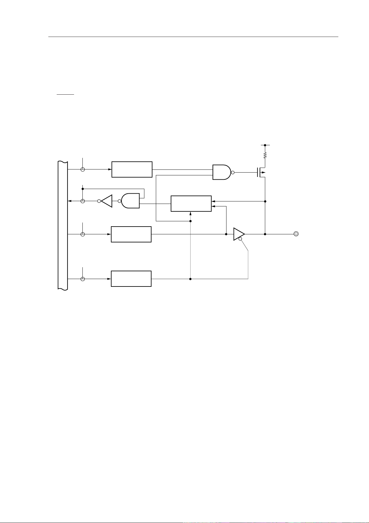
CHAPTER 4 PORT FUNCTIONS
4.2.4 Port 5
Port 5 is an 8-bit input/output port with output latch. P50 to P57 pins can specify the input mode/output mode in
1-bit units with the port mode register 5 (PM5). When P50 to P57 pins are used as input ports, an on-chip pull-up
resistor can be used to them in 8-bit units with a pull-up resistor option register L (PUOL).
A maximum of 7 out of 8 ports can drive LEDs directly.
RESET input sets port 5 to input mode.
Figure 4-6 shows a block diagram of port 5.
Figure 4-6. P50 to P57 Block Diagram
VDD
WR
PUO
RD
WRPORT
Internal bus
WRPM
PUO5
Selector
Output Latch
(P50 to P57)
PM50-PM57
PUO : Pull-up resistor option register
PM : Port mode register
RD : Port 5 read signal
WR : Port 5 write signal
P-ch
P50-P57
59
Page 83

CHAPTER 4 PORT FUNCTIONS
4.2.5 Port 7
This is a 3-bit input/output port with output latches. Input mode/output mode can be specified bit-wise by means
of port mode register 7 (PM7). When pins P70 to P72 are used as input port pins, an on-chip pull-up resistor can
be used as a 3-bit unit by means of pull-up resistor option register L (PUOL).
Dual-functions include serial interface channel 2 data input/output and clock input/output.
RESET input sets the input mode.
Port 7 block diagrams are shown in Figures 4-7 and 4-8.
Caution When used as a serial interface, set the input/output and output latch according to its functions.
For the setting method, refer to Table 11-2 Serial Interface Channel 2 Operating Mode Settings.
Figure 4-7. P70 Block Diagram
VDD
WR
PUO
RD
WRPORT
Internal bus
WRPM
PUO7
Selector
Output Latch
(P70)
PM70
PUO : Pull-up resistor option register
PM : Port mode register
RD : Port 7 read signal
WR : Port 7 write signal
P-ch
P70/SI2/RxD
60
Page 84

WR
CHAPTER 4 PORT FUNCTIONS
Figure 4-8. P71 and P72 Block Diagram
VDD
PUO
RD
WRPORT
Internal bus
WRPM
PUO7
Selector
Output Latch
(P71 and P72)
PM71, PM72
Alternate Function
PUO : Pull-up resistor option register
PM : Port mode register
RD : Port 7 read signal
WR : Port 7 write signal
P-ch
P71/SO2/TxD,
P72/SCK2/ASCK
61
Page 85

CHAPTER 4 PORT FUNCTIONS
4.2.6 Port 10
This is an 2-bit input/output port with output latches. Input mode/output mode can be specified bit-wise by means
of port mode register 10 (PM10). When pins P100 to P101 are used as input port pins, an on-chip pull-up resistor
can be used as an 2-bit unit by means of pull-up resistor option register H (PUOH).
These pins are dual function pins and serve as timer inputs/outputs.
RESET input sets the input mode.
The port 10 block diagram is shown in Figure 4-9.
Figure 4-9. P100 to P101 Block Diagram
VDD
WR
PUO
RD
WRPORT
Internal bus
WRPM
PUO10
Selector
Output Latch
(P100 to P101)
PM100 to PM101
Alternate
Functions
PUO : Pull-up resistor option register
PM : Port mode register
RD : Port 10 read signal
WR : Port 10 write signal
P-ch
P100/TI5/TO5,
P101/TI6/TO6
62
Page 86

CHAPTER 4 PORT FUNCTIONS
4.3 Port Function Control Registers
The following two types of registers control the ports.
• Port mode registers (PM0, PM1, PM3, PM5, PM7, PM10)
• Pull-up resistor option register (PUOH, PUOL)
(1) Port mode registers (PM0, PM1, PM3, PM5, PM7, PM10)
These registers are used to set port input/output in 1-bit units.
PM0, PM1, PM3, PM5, PM7, PM10 are independently set with a 1-bit or 8-bit memory manipulation instruction
RESET input sets registers to FFH.
When port pins are used as the dual-function pins, set the port mode register and output latch according to
Table 4-3.
Cautions 1. P00 pin is input-only pin.
2. As port 0 has a dual function as external interrupt request input, when the port function
output mode is specified and the output level is changed, the interrupt request flag is
set. When the output mode is used, therefore, the interrupt mask flag should be set to
1 beforehand.
63
Page 87
CHAPTER 4 PORT FUNCTIONS
Table 4-3. Port Mode Register and Output Latch Settings when Using Dual-Functions
Pin Name
P01 to P03 INTP1 to INTP3 Input 1 ×
P10 to P17
P35 PCL Output 0 0
P36 BUZ Output 0 0
P100 TI5 Input 1 ×
P101 TI6 Input 1 ×
Note
ANI0 to ANI7 Input 1 ×
TO5 Output 0 0
TO6 Output 0 0
Dual-functions
Name
Input/Output
P××PM××
Note If a read instruction is performed to these pins when they are used as an alternate function, read data is
to be undefined.
Caution When port 7 is used for serial interface, the I/O latch or output latch must be set according to
its function. For the setting methods, see Table 11-2 “Serial Interface Channel 2 Operating Mode
Settings.”
Remarks × : don’t care
PM×× : port mode register
P×× : port output latch
64
Page 88
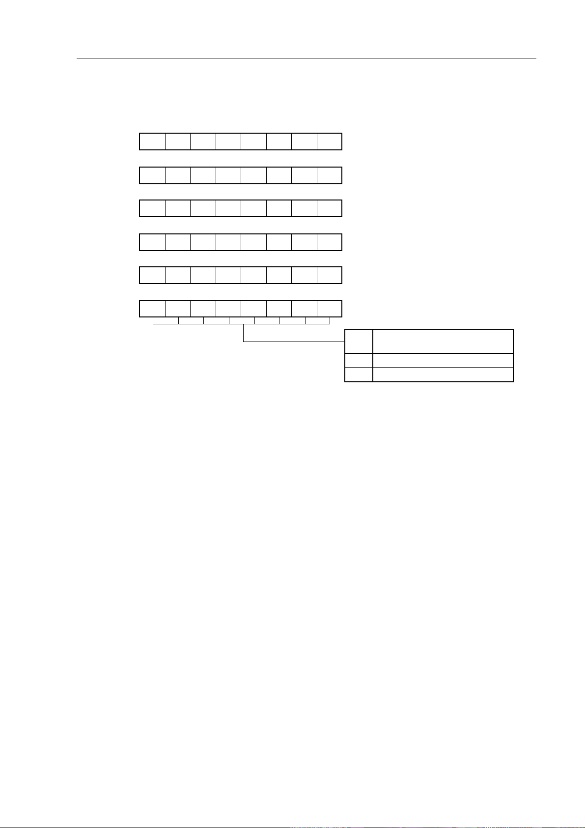
PM0
CHAPTER 4 PORT FUNCTIONS
Figure 4-10. Port Mode Register Format
76543210Symbol
1 1 PM03 PM02 PM01 1
11
Address
FF20H
After
Reset
FFH
R/W
R/W
PM1
PM17 PM16 PM15 PM14 PM13 PM12 PM11 PM10
PM3
PM37 PM36 PM35 PM34 PM33 PM32 PM31 PM30
PM5
PM57 PM56 PM55 PM54 PM53 PM52 PM51 PM50
PM7
PM10
1 1 1 1 1 PM72 PM71 PM70
111111
PM101PM100
FF21H
FF23H
FF25H
FF27H FFH
FF2AH FFH R/W
Pmn Pin Input/Output Mode Selection
PMmn
(m = 0, 1, 3, 5, 7, 10 : n = 0 to 7)
Output mode (output buffer ON)
0
1
Input mode (output buffer OFF)
FFH
FFH
FFH
R/W
R/W
R/W
R/W
Caution Set 1 to the bits 0, 4 to 7 of PM0, bits 3 to 7 of PM7 and bits 2 to 7 of PM10.
65
Page 89

CHAPTER 4 PORT FUNCTIONS
(2) Pull-up resistor option register (PUOH, PUOL)
This register is used to set whether to use an internal pull-up resistor at each port or not. A pull-up resistor
is internally used at bits which are set to the input mode at a port where on-chip pull-up resistor use has been
specified with PUOH, PUOL. No on-chip pull-up resistors can be used to the bits set to the output mode or
to the bits used as an analog input pin, irrespective of PUOH or PUOL setting.
PUOH and PUOL are set with a 1-bit or 8-bit memory manipulation instruction.
RESET input sets this register to 00H.
Cautions 1. P00 pin does not incorporate a pull-up resistor.
2. When port 1 is used as dual-function pin, an on-chip pull-up resistor cannot be used even
if 1 is set in PUOL bit 1 (PUO1).
Figure 4-11. Pull-Up Resistor Option Register Format
After
76 32 0
7654Symbol
00
76 32 0
7654
PUO7 0 PUO5 0 0 PUO1 PUO0PUOL
0 0 PUO10
0
PUO3
1
00PUOH FFF3H 00H R/W
1
Address
FFF7H 00H R/W
Reset
R/W
PUOm
Pm Internal Pull-up Resistor Selection
(m = 0, 1, 3, 5, 7, 10)
Internal pull-up resistor not used
0
1
Internal pull-up resistor used
Caution Set 0 to the bits 0, 1, 3 to 7 of PUOH and bits 2, 4, 6 of PUOL.
66
Page 90

CHAPTER 4 PORT FUNCTIONS
4.4 Port Function Operations
Port operations differ depending on whether the input or output mode is set, as shown below.
4.4.1 Writing to input/output port
(1) Output mode
A value is written to the output latch by a transfer instruction, and the output latch contents are output from
the pin.
Once data is written to the output latch, it is retained until data is written to the output latch again.
(2) Input mode
A value is written to the output latch by a transfer instruction, but since the output buffer is OFF, the pin status
does not change.
Once data is written to the output latch, it is retained until data is written to the output latch again.
Caution In the case of 1-bit memory manipulation instruction, although a single bit is manipulated
the port is accessed as an 8-bit unit. Therefore, on a port with a mixture of input and output
pins, the output latch contents for pins specified as input are undefined except for the
manipulated bit.
4.4.2 Reading from input/output port
(1) Output mode
The output latch contents are read by a transfer instruction. The output latch contents do not change.
(2) Input mode
The pin status is read by a transfer instruction. The output latch contents do not change.
4.4.3 Operations on input/output port
(1) Output mode
An operation is performed on the output latch contents, and the result is written to the output latch. The output
latch contents are output from the pins.
Once data is written to the output latch, it is retained until data is written to the output latch again.
(2) Input mode
The output latch contents are undefined, but since the output buffer is OFF, the pin status does not change.
Caution In the case of 1-bit memory manipulation instruction, although a single bit is manipulated
the port is accessed as an 8-bit unit. Therefore, on a port with a mixture of input and output
pins, the output latch contents for pins specified as input are undefined, even for bits other
than the manipulated bit.
67
Page 91

[MEMO]
CHAPTER 4 PORT FUNCTIONS
68
Page 92

CHAPTER 5 CLOCK GENERATOR
CHAPTER 5 CLOCK GENERATOR
5.1 Clock Generator Functions
The clock generator generates the clock to be supplied to the CPU and peripheral hardware. The following type
of system clock oscillator is available.
Main system clock oscillator
This circuit oscillates at frequencies of 1 to 5.0 MHz. Oscillation can be stopped by executing the STOP instruction.
5.2 Clock Generator Configuration
The clock generator consists of the following hardware.
Table 5-1. Clock Generator Configuration
Item Configuration
Control register Processor clock control register (PCC)
Oscillation mode selection register (OSMS)
Oscillator Main system clock oscillator
69
Page 93

X1
X2
Main
System
Clock
Oscillator
STOP
fX
CHAPTER 5 CLOCK GENERATOR
Figure 5-1. Block Diagram of Clock Generator
Scaler
Selector
X
f
2
f
XX
f
XX
2
Prescaler
fXX
3
fXX
2
2
2
fXX
2
4
Selector
3
Prescaler
Standby
Control
Circuit
Clock to
Peripheral
Hardware
CPU Clock
(f
CPU)
MCS
Oscillation Mode
Selection Register
PCC2
Internal Bus
PCC0
PCC1
Processor Clock Control Register
70
Page 94

CHAPTER 5 CLOCK GENERATOR
0 0 0 0 PCC2 PCC1 PCC0PCC FFFBH 04H R/W
7654Symbol
Address
After
Reset R/W
0
76 32 0
1
0
0f
XX
/2
PCC2
CPU CIock Selection (f
CPU
)
PCC1 PCC0
0
0
0
1
0
0
1
1
0
1
100
f
XX
/2
2
fXX/2
3
fXX/2
4
f
XX
Setting prohibitedOther than above
fx/2 (0.8 s)
µ
fx/22(1.6 s)
µ
fx/23(3.2 s)
µ
fx/24(6.4 s)
µ
f
x
(0.4 s)
µ
fx/22(1.6 s)
µ
fx/23(3.2 s)
µ
fx/24(6.4 s)
µ
fx/25(12.8 s)
µ
fx /2 (0.8 s)
µ
MCS=1 MCS=0
5.3 Clock Generator Control Register
The clock generator is controlled by the following two registers:
• Processor clock control register (PCC)
• Oscillation mode selection register (OSMS)
(1) Processor clock control register (PCC)
The PCC sets whether to use CPU clock selection and the ratio of division.
The PCC is set with a 1-bit or 8-bit memory manipulation instruction.
RESET input sets the PCC to 04H.
Figure 5-2. Processor Clock Control Register Format
Caution Set 0 to the bits 3 to 7.
Remarks 1. f
XX : Main system clock frequency (fX or fX/2)
X : Main system clock oscillator frequency
2. f
3. MCS : Bit 0 of oscillation mode selection register (OSMS)
4. Figures in parentheses indicate minimum instruction execution time : 2f
X = 5.0 MHz.
at f
CPU when operating
71
Page 95

CHAPTER 5 CLOCK GENERATOR
(2) Oscillation mode selection register (OSMS)
This register specifies whether the clock output from the main system clock oscillator without passing through
the scaler is used as the main system clock, or the clock output via the scaler is used as the main system
clock.
OSMS is set with 8-bit memory manipulation instruction.
RESET input sets OSMS to 00H.
Figure 5-3. Oscillation Mode Selection Register Format
1
765432Symbol
000 0OSMS FFF2H
0 MCS
0
0
0
Address
Main System Clock Scaler Control
MCS
Scaler used
0
1
Scaler not used
After
Reset
00H W
R/W
Cautions 1. Writing to OSMS should be performed only immediately after reset signal release and before
peripheral hardware operation starts. As shown in Figure 5-4 below, writing data (including
same data as previous) to OSMS cause delay of main system clock cycle up to 2/f
x during
the write operation. Therefore, if this register is written during the operation, in peripheral
hardware which operates with the main system clock, a temporary error occurs in the count
clock cycle of timer, etc. In addition, because the oscillation mode is changed by this register,
the clocks for peripheral hardware as well as that for the CPU are switched.
Figure 5-4. Main System Clock Waveform due to Writing to OSMS
Write to OSMS
(MCS 0)
Max. 2/fX
fXX
Remarks f
Operating at fXX = fX/2 (MCS = 0) Operating at fXX = fX/2 (MCS = 0)
2. When writing “1” to MCS, V
xx : Main system clock frequency (fx or fx/2)
x : Main system clock oscillation frequency
f
DD must be 2.7 V or higher before the write execution.
72
Page 96

CHAPTER 5 CLOCK GENERATOR
5.4 System Clock Oscillator
5.4.1 Main system clock oscillator
The main system clock oscillator oscillates with a crystal resonator or a ceramic resonator (standard: 5.0 MHz)
connected to the X1 and X2 pins.
External clocks can be input to the main system clock oscillator. In this case, input a clock signal to the X1 pin
and an antiphase clock signal to the X2 pin.
Figure 5-5 shows an external circuit of the main system clock oscillator.
Figure 5-5. External Circuit of Main System Clock Oscillator
(a) Crystal and ceramic oscillation (b) External clock
Crystal
or
Ceramic Resonator
IC
X2
X1
External
Clock
PD74HCU04
µ
X2
X1
Cautions 1. Do not execute the STOP instruction if an external clock is used. This is because the X2 pin
is connected to V
DD via a pull-up register.
2. When using a main system clock oscillator, carry out wiring in the broken line area in Figure
5-5 to prevent any effects from wiring capacities.
● Minimize the wiring length.
● Do not allow wiring to intersect with other signal conductors. Do not allow wiring to come
near changing high current.
● Set the potential of the grounding position of the oscillator capacitor to that of VSS. Do
not ground to any ground pattern where high current is present.
● Do not fetch signals from the oscillator.
Figure 5-6 shows examples of oscillator having bad connection.
73
Page 97

CHAPTER 5 CLOCK GENERATOR
Figure 5-6. Examples of Oscillator with Bad Connection (1/2)
(a) Wiring of connection circuits (b) Signal conductors intersect
is too long with each other
PORTn
X2 X1
IC X2 X1
(n = 0, 1, 3, 5, 7, 10)
IC
(c) Changing high current is too near a (d) Current flows through the grounding line
signal conductor of the ocsillator (potential at points A, B,
and C fluctuate)
DD
V
74
IC X2 X1
High
Current
IC X2
AB C
High
Current
X1
Pnm
Page 98

Figure 5-6. Examples of Oscillator with Bad Connection (2/2)
(c) Signals are fetched
IC X2 X1
CHAPTER 5 CLOCK GENERATOR
5.4.2 Scaler
The scaler divides the main system clock oscillator output (fXX) and generates various clocks.
75
Page 99

CHAPTER 5 CLOCK GENERATOR
5.5 Clock Generator Operations
The clock generator generates the following various types of clocks and controls the CPU operating mode
including the standby mode.
• Main system clock fXX
• CPU clock fCPU
• Clock to peripheral hardware
The following clock generator functions and operations are determined with the processor clock control register
(PCC) and the oscillation mode selection register (OSMS).
µ
(a) Upon generation of RESET signal, the lowest speed mode of the main system clock (12.8
at 5.0 MHz) is selected (PCC = 04H, OSMS = 00H). Main system clock oscillation stops while low level is
applied to RESET pin.
µ
(b) The six types of CPU clocks (0.4
the PCC and OSMS.
s. 0.8 µs, 1.6 µs, 3.2 µs, 6.4µs, 12.8 µs : 5.0 MHz) can be selected by setting
s when operated
(c) Two standby modes, the STOP and HALT modes, are available.
(d) The main system clock is divided and supplied to the peripheral hardware. Thus, the peripheral hardware
also stops if the main system clock is stopped. (Except external input clock operation)
76
Page 100

CHAPTER 5 CLOCK GENERATOR
5.6 Changing CPU Clock Settings
5.6.1 Time required for CPU clock switchover
The CPU clock can be switched over by means of bits 0 to 2 (PCC0 to PCC2) of the processor clock control register
(PCC).
The actual switchover operation is not performed directly after writing to the PCC, but operation continues on the
pre-switchover clock for several instructions (see Table 5-2).
Table 5-2. Maximum Time Required for CPU Clock Switchover
Set Values before
Switchover
PCC0PCC2 PCC1
000 16 instructions 16 instructions 16 instructions 16 instructions
0
011
1
1
0
1
00
00
8 instructions
4 instructions 4 instructions
2 instructions
2 instructions
1 instruction 1 instruction1 instruction
Set Values After Switchover
8 instructions 8 instructions
2 instructions
8 instructions
4 instructions 4 instructions
1 instruction
PCC1PCC2 PCC0PCC1PCC2 PCC0PCC1PCC2 PCC0PCC1PCC2 PCC0PCC1PCC2 PCC0
100110100100000
2 instructions
Remark One instruction is the minimum instruction execution time with the pre-switchover CPU clock.
77
 Loading...