

Page 1

International Technical Support Organization
IBM PC Server and Novell NetWare Integration Guide
December 1995
SG24-4576-00
Page 2

Take Note!
Before using this information and the product it supports, be sure to read the general information under
“Special Notices” on page xv.
First Edition (December 1995)
This edition applies to IBM PC Servers, for use with an OEM operating system.
Order publications through your IBM representative or the IBM branch office serving your locality. Publications
are not stocked at the address given below.
An ITSO Technical Bulletin Evaluation Form for reader′s feedback appears facing Chapter 1. If the form has been
removed, comments may be addressed to:
IBM Corporation, International Technical Support Organization
Dept. HZ8 Building 678
P.O. Box 12195
Research Triangle Park, NC 27709-2195
When you send information to IBM, you grant IBM a non-exclusive right to use or distribute the information in any
way it believes appropriate without incurring any obligation to you.
Copyright International Business Machines Corporation 1995. All rights reserved.
Note to U.S. Government Users — Documentation related to restricted rights — Use, duplication or disclosure is
subject to restrictions set forth in GSA ADP Schedule Contract with IBM Corp.
Page 3

Abstract
This document describes the procedures necessary to successfully implement
Novell NetWare on an IBM PC Server platform. It describes the current IBM PC
Server line and discusses the technology inside the machines. It outlines
step-by-step procedures for installing both NetWare V3.12 and V4.1 using both
IBM ServerGuide and the original product media. It has a detailed section on
performance tuning. It covers IBM′s NetFinity systems management tool, which
ships with every IBM PC Server and IBM premium brand PC.
This document is intended for IBM customers, dealers, systems engineers and
consultants who are implementing NetWare on an IBM PC Server platform.
A basic knowledge of PCs, file servers, DOS, and NetWare is assumed.
(212 pages)
Copyright IBM Corp. 1995 iii
Page 4

Contents
Abstract . . . . . . . . . . . . . . . . . . . . . . . . . . . . . . . . . . . . . . . . . . iii
Special Notices
Preface
How This Document is Organized
Related Publications
. . . . . . . . . . . . . . . . . . . . . . . . . . . . . . . . . . . . . . xv
. . . . . . . . . . . . . . . . . . . . . . . . . . . . . . . . . . . . . . . . . xvii
......................... xvii
. . . . . . . . . . . . . . . . . . . . . . . . . . . . . . . . xviii
International Technical Support Organization Publications
ITSO Redbooks on the World Wide Web (WWW)
Acknowledgments
. . . . . . . . . . . . . . . . . . . . . . . . . . . . . . . . . . . xix
Chapter 1. IBM PC Server Technologies
1.1 Processors
1.1.1 Clock Rate
1.1.2 External Interfaces
1.1.3 Processor Types
1.2 Multiprocessing
1.3 Memory
1.3.1 Caches
1.3.2 Memory Interleaving
1.3.3 Dual Path Buses
1.3.4 SynchroStream Technology
. . . . . . . . . . . . . . . . . . . . . . . . . . . . . . . . . . . . . . 1
. . . . . . . . . . . . . . . . . . . . . . . . . . . . . . . . . . . 1
. . . . . . . . . . . . . . . . . . . . . . . . . . . . . . 2
. . . . . . . . . . . . . . . . . . . . . . . . . . . . . . . . 2
. . . . . . . . . . . . . . . . . . . . . . . . . . . . . . . . . . . 3
. . . . . . . . . . . . . . . . . . . . . . . . . . . . . . . . . . . . . . . 3
. . . . . . . . . . . . . . . . . . . . . . . . . . . . . . . . . . . . . 4
. . . . . . . . . . . . . . . . . . . . . . . . . . . . . 6
................................ 7
. . . . . . . . . . . . . . . . . . . . . . . . . 8
1.4 Memory Error Detection and Correction
1.4.1 Standard (Parity) Memory
1.4.2 Error Correcting Code (ECC)
.......................... 9
........................ 9
................ xviii
...................... 1
.................... 9
1.4.3 Error Correcting Code-Parity Memory (ECC-P)
1.4.4 ECC on SIMMs (EOS) Memory
1.4.5 Performance Impact
. . . . . . . . . . . . . . . . . . . . . . . . . . . . . 12
1.4.6 Memory Options and Speed
1.5 Bus Architectures
1.5.1 ISA Bus
1.5.2 EISA Bus
1.5.3 Micro Channel Bus
1.5.4 P CI B u s
1.6 Disk Subsystem
. . . . . . . . . . . . . . . . . . . . . . . . . . . . . . . . . 12
. . . . . . . . . . . . . . . . . . . . . . . . . . . . . . . . . . . . . 13
. . . . . . . . . . . . . . . . . . . . . . . . . . . . . . . . . . . . 13
.............................. 13
. . . . . . . . . . . . . . . . . . . . . . . . . . . . . . . . . . . . . 15
. . . . . . . . . . . . . . . . . . . . . . . . . . . . . . . . . . . 16
1.6.1 Hard Disk Interfaces
1.6.2 SCSI Technology
1.6.3 SCSI Adapters
1.6.4 Hard Disk Drives
1.6.5 RAID Technology
1.6.6 RAID Classifications
1.6.7 Recommendations
1.7 LAN Subsystem
. . . . . . . . . . . . . . . . . . . . . . . . . . . . . . . 17
. . . . . . . . . . . . . . . . . . . . . . . . . . . . . . . . . 19
............................... 21
. . . . . . . . . . . . . . . . . . . . . . . . . . . . . . . 22
. . . . . . . . . . . . . . . . . . . . . . . . . . . . . 23
. . . . . . . . . . . . . . . . . . . . . . . . . . . . . . 31
. . . . . . . . . . . . . . . . . . . . . . . . . . . . . . . . . . . 31
1.7.1 Shared RAM Adapters
1.7.2 Bus Master Adapters
1.7.3 PeerMaster Technology
1.8 Security Features
. . . . . . . . . . . . . . . . . . . . . . . . . . . . . . . . . . 34
1.8.1 Tamper-Evident Cover
1.8.2 Secure I/O Cables
1.8.3 Passwords
. . . . . . . . . . . . . . . . . . . . . . . . . . . . . . . . . . . 35
............................... 35
1.8.4 Secure Removable Media
............................. 16
............................ 31
............................. 32
. . . . . . . . . . . . . . . . . . . . . . . . . . . 33
. . . . . . . . . . . . . . . . . . . . . . . . . . . . 35
....................... 11
......................... 12
.......................... 36
.......... xviii
.............. 10
Copyright IBM Corp. 1995 v
Page 5

1.8.5 Selectable Drive Startup ........................... 37
1.8.6 Unattended Start Mode
1.9 Systems Management
1.9.1 DMI
1.9.2 SNMP
1.9.3 NetFinity
1.9.4 SystemView
1.10 Fault Tolerance
. . . . . . . . . . . . . . . . . . . . . . . . . . . . . . . . . . . . . . . 37
. . . . . . . . . . . . . . . . . . . . . . . . . . . . . . . . . . . . . . 39
. . . . . . . . . . . . . . . . . . . . . . . . . . . . . . . . . . . . 41
. . . . . . . . . . . . . . . . . . . . . . . . . . . . . . . . . . 45
. . . . . . . . . . . . . . . . . . . . . . . . . . . . . . . . . . 47
1.10.1 NetWare SFT III
1.11 Uninterruptible Power Supply (UPS)
1.11.1 A PC PowerChute
............................ 37
. . . . . . . . . . . . . . . . . . . . . . . . . . . . . . . 37
................................ 48
...................... 52
. . . . . . . . . . . . . . . . . . . . . . . . . . . . . . . 53
Chapter 2. IBM PC Server Family Overview
2.1 IBM PC Server Model Specifications
2.1.1 IBM PC Server 300
2.1.2 IBM PC Server 310
2.1.3 IBM PC Server 320 EISA
2.1.4 IBM PC Server 320 MCA
2.1.5 IBM PC Server 500
2.1.6 IBM PC Server 520 EISA
2.1.7 IBM PC Server 520 MCA
2.1.8 IBM PC Server 720
Chapter 3. Hardware Configuration
3.1 The Setup Program
3.1.1 Main Menu
. . . . . . . . . . . . . . . . . . . . . . . . . . . . . . . . . . . 67
3.1.2 Advanced Menu
3.1.3 Security
. . . . . . . . . . . . . . . . . . . . . . . . . . . . . . . . . . . . . 71
3.2 EISA Configuration Utility
3.3 SCSI Select Utility Program
3.4 System Programs
.............................. 56
.............................. 57
........................... 58
........................... 59
.............................. 60
........................... 61
........................... 62
.............................. 63
. . . . . . . . . . . . . . . . . . . . . . . . . 65
................................ 67
. . . . . . . . . . . . . . . . . . . . . . . . . . . . . . . . 68
............................. 74
............................ 78
.................................. 82
3.4.1 Starting From the System Partition
3.4.2 Starting From the Reference Diskette
3.4.3 Main Menu Options
.............................. 84
3.4.4 Backup/Restore System Programs Menu
3.4.5 Set Configuration Menu
3.4.6 Set Features Menu
3.4.7 Test the Computer
3.4.8 More Utilities Menu
3.4.9 Advanced Diagnostic Program
3.5 RAID Controller Utility
3.5.1 Drive Information
. . . . . . . . . . . . . . . . . . . . . . . . . . . . . . 103
3.5.2 Formatting the Disks
3.5.3 Defining a Hot-Spare Disk
3.5.4 Creating a Disk Array
3.5.5 Defining Logical Drives
3.5.6 Setting the Write Policy
3.5.7 Initializing the Array
........................... 86
.............................. 91
.............................. 97
.............................. 98
....................... 99
.............................. 101
............................ 104
......................... 106
........................... 108
........................... 109
.......................... 112
............................ 112
3.5.8 Backup/Restoring the Configuration
.................... 55
...................... 56
..................... 83
................... 84
................. 86
................... 112
Chapter 4. Novell NetWare Installation
4.1 ServerGuide Overview
4.2 Starting ServerGuide
4.3 Installing NetWare 4.1 with ServerGuide
4.4 Installing NetWare 3.12 with Diskettes
vi NetWare Integration Guide
...................... 115
. . . . . . . . . . . . . . . . . . . . . . . . . . . . . . 115
............................... 115
................... 118
.................... 127
Page 6

4.4.1 Hardware Requirements . . . . . . . . . . . . . . . . . . . . . . . . . . 127
4.4.2 Software Requirements
4.4.3 Information Requested at Time of Installation
4.4.4 Installation Files
4.4.5 Installation Procedure
4.5 Installing NetWare 4.1 with the Original CD-ROM
4.5.1 Hardware Requirements
4.5.2 Software Requirements
4.5.3 Installation Procedure
4.6 NetFinity Services for NetWare
4.6.1 System Requirements
4.6.2 Installing NetFinity Services for NetWare
4.7 The RAID Administration for NetWare Utility
4.7.1 Installing the Utility
4.8 Hard Disk Failure Simulation
4.8.1 Simulating with a Hot Spare Drive
4.8.2 Simulating without a Hot Spare Drive
. . . . . . . . . . . . . . . . . . . . . . . . . . 127
............. 127
. . . . . . . . . . . . . . . . . . . . . . . . . . . . . . . 127
. . . . . . . . . . . . . . . . . . . . . . . . . . . 128
.............. 135
. . . . . . . . . . . . . . . . . . . . . . . . . . 135
. . . . . . . . . . . . . . . . . . . . . . . . . . 135
. . . . . . . . . . . . . . . . . . . . . . . . . . . 135
......................... 144
. . . . . . . . . . . . . . . . . . . . . . . . . . . 144
................ 144
................. 151
............................. 151
.......................... 152
.................... 153
.................. 160
Chapter 5. Performance Tuning
5.1 Hardware Tuning
. . . . . . . . . . . . . . . . . . . . . . . . . . . . . . . . . 167
5.1.1 General Performance Characteristics
5.2 Performance Analysis Tools
5.2.1 DatagLANce
. . . . . . . . . . . . . . . . . . . . . . . . . . . . . . . . . 172
5.2.2 NetWare Monitoring Tools
5.3 Tuning NetWare
5.3.1 Disk Subsystem
. . . . . . . . . . . . . . . . . . . . . . . . . . . . . . . . . . 175
. . . . . . . . . . . . . . . . . . . . . . . . . . . . . . . 176
5.3.2 Network Subsystem
5.3.3 System Memory
. . . . . . . . . . . . . . . . . . . . . . . . . . . . . . . 185
5.3.4 Memory Requirements
5.3.5 System Processor
Appendix A. EISA Configuration File
. . . . . . . . . . . . . . . . . . . . . . . . . . 167
.................. 168
.......................... 172
......................... 173
. . . . . . . . . . . . . . . . . . . . . . . . . . . . . 182
. . . . . . . . . . . . . . . . . . . . . . . . . . . 187
. . . . . . . . . . . . . . . . . . . . . . . . . . . . . . 187
....................... 189
Appendix B. Hardware Compatibility, Device Driver, and Software Patch
Information . . . . . . . . . . . . . . . . . . . . . . . . . . . . . . . . . . . . . . 199
B.1 Finding Compatibility Information on the World Wide Web
B.2 Finding Device Drivers on the World Wide Web
B.3 Finding Software Patches on the World Wide Web
Appendix C. Configuring DOS CD-ROM Support
C.1 Installing CD-ROM Support for PCI Adapters.
C.2 Installing CD-ROM Support for Adaptec Adapters
.............. 200
............. 201
................ 203
................ 203
............. 203
C.3 Installing CD-ROM Support for Micro-Channel Adapters
........ 199
......... 203
List of Abbreviations
Index
. . . . . . . . . . . . . . . . . . . . . . . . . . . . . . . . . . . . . . . . . . . 207
................................. 205
Contents vii
Page 7

Figures
1. SMP Shared Secondary Cache ......................... 5
2. SMP with Dedicated Secondary Cache
3. Two-Way Interleaved Memory Banks
4. Dual Path Bus Implementation
5. ECC Memory Operation
6. ECC-P Memory Implementation
7. Micro Channel - Basic Data Transfer (20 MBps)
8. Micro Channel - Data Streaming Transfer (40 MBps)
9. Micro Channel - Data Streaming Transfer (80 MBps)
10. SCSI Disk Interface
11. RAID-0 (Block Interleave Data Striping without Parity)
12. RAID-1 (Disk Mirroring)
13. RAID-1 (Disk Duplexing)
14. RAID-1 Enhanced, Data Strip Mirroring
15. RAID-6,10 - Mirroring of RAID 0 Drives
16. RAID-2 (Bit Interleave Data Striping with Hamming Code)
17. RAID-3 (Bit Interleave Data Striping with Parity Disk)
18. RAID-4 (Block Interleave Data Striping with One Parity Disk)
19. RAID-5 (Block Interleave Data Striping with Skewed Parity)
20. NetFinity Services Folder
21. IBM PC Server Family of Products
22. Hardware Configuration Steps
23. PC Server 320 Setup Program - Main Menu
24. PC Server 320 Setup Program - Advanced Menu
25. PC Server 320 Setup Program - Boot Options Menu
26. PC Server 320 Setup Program - Integrated Peripherals Menu
27. PC Server 320 Setup Program - Security Menu
28. EISA Configuration Utility - Main Panel
29. EISA Configuration Utility - Steps
30. EISA Configuration Utility - Step 2
31. EISA Configuration Utility - Move Confirmation Panel
32. EISA Configuration Utility - Step 3
33. EISA Configuration Utility - Step 4
34. IBM PC Server SCSISelect Utility Program - Main Menu
35. IBM PC Server SCSI Select Utility Program - Host Adapter Settings
36. PC Server 320 SCSI Select Utility Program - SCSI Device Configuration 80
37. PC Server 320 SCSISelect Utility Program - Advanced Configuration
38. PC Server 320 SCSISelect Utility Program - DASD Information
39. System Programs - Main Menu
40. System Programs - Backup/Restore System Programs Menu
41. System Programs - Set Configuration Menu
42. System Programs - View Configuration Screen
43. Set Configuration - Memory Map
44. Set Configuration - SCSI Device Configuration
45. Set Features Menu
46. Set Passwords and Security Features
47. Set Startup Sequence Screen
48. Set Power-On Features Screen
49. More Utilities Menu
50. Display Revision Level Screen
51. System Error Log Screen
. . . . . . . . . . . . . . . . . . . . 6
. . . . . . . . . . . . . . . . . . . . . 7
. . . . . . . . . . . . . . . . . . . . . . . . . 8
. . . . . . . . . . . . . . . . . . . . . . . . . . . . . 10
. . . . . . . . . . . . . . . . . . . . . . . . 11
. . . . . . . . . . . . . . 14
. . . . . . . . . . . . 14
. . . . . . . . . . . . 15
................................ 17
........... 24
............................. 25
............................. 25
.................... 26
.................... 26
........ 27
........... 28
....... 29
....... 29
............................ 41
....................... 55
......................... 66
................. 67
.............. 68
............ 69
...... 70
............... 71
.................... 74
....................... 74
....................... 75
........... 75
....................... 76
....................... 77
......... 78
.. 78
.. 81
...... 82
........................ 84
...... 86
................. 87
............... 88
........................ 90
............... 91
................................ 92
..................... 93
.......................... 96
......................... 97
................................ 98
......................... 98
............................ 99
Copyright IBM Corp. 1995 ix
Page 8

52. Advanced Diagnostic Menu .......................... 100
53. Test Selection Menu
54. RAID Configuration Program - Adapter Selection
55. RAID Configuration Program - Main Menu
56. RAID Configuration Program - Drive Information
57. RAID Configuration Program - Advanced Functions Menu
58. RAID Configuration Program - DASD Formatting
59. RAID Configuration Program - Change RAID parameters
60. RAID Configuration Program - Create/Delete Array Menu
61. RAID Configuration Program - Hot-Spare Disk Definition
62. RAID Configuration Program - Disk Array Creation
63. RAID Configuration Program - Logical Drive Definition
.............................. 100
............. 102
................. 102
............. 103
........ 104
............. 105
........ 105
........ 107
........ 107
............ 108
......... 109
64. RAID Configuration Program - Logical Drive Definition - Array
Selection
65. RAID Configuration Program - RAID level Selection
66. RAID Configuration Program - Size Definition
67. RAID Configuration Program - Result
68. RAID Configuration Program - Advanced Functions Menu
69. ServerGuide Language
70. ServerGuide Main Menu
71. Installing NetWare
72. Configuring NetWare
73. Configuring IBM NetFinity
74. Partitioning the Hard Disk
75. Reviewing Configuration
76. Unlocking Programs
77. Installing NetWare Directory Services (NDS)
78. Assigning a Name to a Directory Tree
79. Assigning a Context for the Server
80. Server Context Information.
81. NetWare Installation
82. NetWare V3.12 Installation - Main Menu
83. Create Partition
84. Partition Information
85. Creating a New Volume
86. Volume Status
87. Copy System and Public Files
88. Path for STARTUP.NCF File
89. STARTUP.NCF File
90. AUTOEXEC.NCF File
91. Installation Menu
92. Disk Driver Options
93. Network Driver Options
94. Create Partition
95. Disk Partition Information
96. New Volume Information
97. Optional NetWare Files
98. Install NetWare Directory Services(NDS)
99. Assigning a Name to the Directory Tree
100. Context for the Server
101. Server Context Information
102. Editing STARTUP.NCF File
103. Editing AUTOEXEC.NCF File
104. File Copy Status
105. Other Installation Options
. . . . . . . . . . . . . . . . . . . . . . . . . . . . . . . . . . . . . 109
........... 110
............... 111
.................... 111
........ 113
. . . . . . . . . . . . . . . . . . . . . . . . . . . . 116
............................ 117
. . . . . . . . . . . . . . . . . . . . . . . . . . . . . . . 119
. . . . . . . . . . . . . . . . . . . . . . . . . . . . . . 120
........................... 121
........................... 122
. . . . . . . . . . . . . . . . . . . . . . . . . . . . 123
. . . . . . . . . . . . . . . . . . . . . . . . . . . . . . 124
................ 125
................... 125
..................... 126
.......................... 126
. . . . . . . . . . . . . . . . . . . . . . . . . . . . . . 129
.................. 130
. . . . . . . . . . . . . . . . . . . . . . . . . . . . . . . . . 130
. . . . . . . . . . . . . . . . . . . . . . . . . . . . . . 131
............................ 131
. . . . . . . . . . . . . . . . . . . . . . . . . . . . . . . . . . 132
........................ 132
.......................... 133
. . . . . . . . . . . . . . . . . . . . . . . . . . . . . . . 134
. . . . . . . . . . . . . . . . . . . . . . . . . . . . . . 134
. . . . . . . . . . . . . . . . . . . . . . . . . . . . . . . . 136
............................... 137
............................ 137
. . . . . . . . . . . . . . . . . . . . . . . . . . . . . . . . . 138
........................... 138
............................ 139
............................ 139
.................. 140
.................. 140
............................. 141
.......................... 141
........................... 142
.......................... 142
................................. 143
........................... 143
x NetWare Integration Guide
Page 9

106. NetFinity Network Driver Configuration ................... 145
107. NetFinity Installation
108. NetFinity Services for NetWare
109. NetFinity Installation - Copying Files
110. Network Driver Configuration
111. Configuration Update
112. NetFinity Installation Complete
113. Raid Administration for NetWare - Main Menu
114. RAID Administration Utility - Main Menu
115. Verifying Array Configuration
116. Using RAID Manager to View Array Configuration
117. Detecting the Disk Failure
118. Disk Failure - NetFinity Alert
119. Disk Failure - NetFinity RAID Service
120. View Last Event Message
121. RAID Administration - Recovery Message
122. NetFinity Recovery Alert
123. Changes in Array Configuration
124. RAID Administration - Replace a Defunct Drive
125. RAID Administration - Verifying the Replacement of a Defunct Drive
126. NetFinity New Hot Spare Drive Alert
127. NetFinity RAID Service - New Hot Spare
128. RAID Administration - Array Configuration
129. NetFinity RAID Service - Verifying Configuration
130. Detecting the Disk Failure
131. NetFinity Alert Log
132. NetFinity RAID Service - Disk Failure
133. Last Event Message
134. RAID Administration Utility - Reviewing Disk Status
135. RAID Administration - Replace a Defunct Drive
136. RAID Administration - Rebuild Progress
137. RAID Administration - Verifying the Rebuild Status
138. NetFinity Alert - New Disk Online
139. LAN Server Controlled Subsystems
140. File Server Performance - General Characteristics
141. Differences in LAN Adapters
142. Differences in Disk Subsystems
143. MONITOR Utility
. . . . . . . . . . . . . . . . . . . . . . . . . . . . . . . . . 174
144. SERVMAN Utility
145. Sample Compatibility Report Showing Ethernet LAN Adapters
. . . . . . . . . . . . . . . . . . . . . . . . . . . . . . 147
........................ 148
..................... 148
......................... 149
. . . . . . . . . . . . . . . . . . . . . . . . . . . . . . 150
........................ 150
.............. 152
.................. 153
......................... 154
............ 154
........................... 155
......................... 155
.................... 156
........................... 156
................. 157
............................ 157
....................... 158
.............. 158
. 159
..................... 159
.................. 160
................. 160
............. 161
........................... 161
............................... 162
.................... 162
.............................. 163
........... 163
.............. 164
.................. 164
............ 165
...................... 165
..................... 167
............ 169
......................... 171
....................... 172
. . . . . . . . . . . . . . . . . . . . . . . . . . . . . . . . 175
..... 200
Figures xi
Page 10

Tables
1. ECC Memory Performances . . . . . . . . . . . . . . . . . . . . . . . . . . . 12
2. Summary of Memory Implementations
3. SCSI Adapters Summary
4. PCI SCSI Adapters Summary
5. Summary of Disks Performance Characteristics
6. RAID Classifications
7. Summary of RAID Performance Characteristics
8. IBM PC Servers 300 Models
9. IBM PC Servers 310 Models
10. IBM PC Servers 320 EISA Models
11. IBM PC Servers 320 MCA Models
12. IBM PC Server 500 Models
13. IBM PC Servers 520 EISA Models
14. IBM PC Servers 520 MCA Models
15. IBM PC Servers 720 Models
16. Host Adapter SCSI Termination Parameter
17. Volume Block Size and Cache Buffer Size Recommendations
18. Default Block Sizes Based on Volume Size
19. NetWare Memory Pools
. . . . . . . . . . . . . . . . . . . . 12
. . . . . . . . . . . . . . . . . . . . . . . . . . . . 21
. . . . . . . . . . . . . . . . . . . . . . . . . . 21
. . . . . . . . . . . . . . 22
. . . . . . . . . . . . . . . . . . . . . . . . . . . . . . . 23
. . . . . . . . . . . . . . . 30
. . . . . . . . . . . . . . . . . . . . . . . . . . 56
. . . . . . . . . . . . . . . . . . . . . . . . . . 57
....................... 58
....................... 59
........................... 60
....................... 61
....................... 62
.......................... 63
................. 79
..... 176
................ 177
............................ 185
Copyright IBM Corp. 1995 xiii
Page 11

Special Notices
This document is intended for IBM customers, dealers, systems engineers and
consultants who are implementing Novell NetWare on an IBM PC Server. The
information in this publication is not intended as the specification of any
programming interfaces that are provided by IBM.
References in this publication to IBM products, programs or services do not
imply that IBM intends to make these available in all countries in which IBM
operates. Any reference to an IBM product, program, or service is not intended
to state or imply that only IBM′s product, program, or service may be used. Any
functionally equivalent program that does not infringe any of IBM′s intellectual
property rights may be used instead of the IBM product, program or service.
Information in this book was developed in conjunction with use of the equipment
specified, and is limited in application to those specific hardware and software
products and levels.
IBM may have patents or pending patent applications covering subject matter in
this document. The furnishing of this document does not give you any license to
these patents. You can send license inquiries, in writing, to the IBM Director of
Licensing, IBM Corporation, 500 Columbus Avenue, Thornwood, NY 10594 USA.
The information contained in this document has not been submitted to any
formal IBM test and is distributed AS IS. The information about non-IBM
(VENDOR) products in this manual has been supplied by the vendor and IBM
assumes no responsibility for its accuracy or completeness. The use of this
information or the implementation of any of these techniques is a customer
responsibility and depends on the customer′s ability to evaluate and integrate
them into the customer′s operational environment. While each item may have
been reviewed by IBM for accuracy in a specific situation, there is no guarantee
that the same or similar results will be obtained elsewhere. Customers
attempting to adapt these techniques to their own environments do so at their
own risk.
Any performance data contained in this document was determined in a
controlled environment, and therefore, the results that may be obtained in other
operating environments may vary significantly. Users of this document should
verify the applicable data for their specific environment.
Reference to PTF numbers that have not been released through the normal
distribution process does not imply general availability. The purpose of
including these reference numbers is to alert IBM customers to specific
information relative to the implementation of the PTF when it becomes available
to each customer according to the normal IBM PTF distribution process.
The following terms are trademarks of the International Business Machines
Corporation in the United States and/or other countries:
AIX AIX/6000
AT DB2/2
DataHub DatagLANce
EtherStreamer First Failure Support Technology
IBM LANStreamer
Micro Channel NetFinity
Copyright IBM Corp. 1995 xv
Page 12

NetView OS/2
PS/2 Personal System/2
Power Series 800 Presentation Manager
SystemView Ultimedia
VM/ESA
The following terms are trademarks of other companies:
C-bus is a trademark of Corollary, Inc.
PC Direct is a trademark of Ziff Communications Company and is
used by IBM Corporation under license.
UNIX is a registered trademark in the United States and other
countries licensed exclusively through X/Open Company Limited.
Windows is a trademark of Microsoft Corporation.
386 Intel Corporation
486 Intel Corporation
AHA Adaptec, Incorporated
AppleTalk Apple Computer, Incorporated
Banyan Banyan Systems, Incorporated
CA Computer Associates
DECnet Digital Equipment Corporation
EtherLink 3COM Corporation
HP Hewlett-Packard Company
IPX Novell, Incorporated
Intel Intel Corporation
Lotus 1-2-3 Lotus Development Corporation
Lotus Notes Lotus Development Corporation
MS Microsoft Corporation
Micronics Micronics Electronics, Incorporated
Microsoft Microsoft Corporation
Microsoft Excel Microsoft Corporation
NFS Sun Microsystems Incorporated
NetWare Novell, Incorporated
Novell Novell, Incorporated
OpenView Hewlett-Packard Company
Pentium Intel Corporation
Phoenix Phoenix Technologies, Limited
PowerChute American Power Conversion
SCO The Santa Cruz Operation, Incorporated
SCSI Security Control Systems, Incorporated
SCSISelect Ada ptec, Incorporated
VINES Banyan Systems, Incorporated
Windows NT Microsoft Corporation
X/Open X/Open Company Limited
i386 Intel Corporation
i486 Intel Corporation
i960 Intel Corporation
Other trademarks are trademarks of their respective companies.
xvi NetWare Integration Guide
Page 13

Preface
This document describes the procedures necessary to implement Novell
NetWare on IBM PC Server platforms. It provides detailed information on
installation, configuration, performance tuning, and management of the IBM PC
Server in the NetWare environment. It also discusses the features and
technologies of the IBM PC Server brand and positions the various models in the
brand.
How This Document is Organized
The document is organized as follows:
•
Chapter 1, “IBM PC Server Technologies”
This chapter introduces many of the technologies used in the IBM PC Server
brand and gives examples of system implementations where they are used.
•
Chapter 2, “IBM PC Server Family Overview”
This chapter positions the various models within the IBM PC Server brand
and gives specifications for each model.
•
Chapter 3, “Hardware Configuration”
This chapter provides a roadmap for configuring the various models of the
IBM PC Server line and describes the configuration process in detail.
•
Chapter 4, “Novell NetWare Installation”
This chapter gives a step-by-step process for installing both NetWare V3.12
and V4.1 and the NetFinity Manager using both ServerGuide and the original
product diskettes and CD-ROM. It also contains an overview of the
ServerGuide product. It also covers the RAID administration tools and
details a process for simulating and recovering from a DASD failure.
•
Chapter 5, “Performance Tuning”
This chapter presents an in-depth discussion of tuning NetWare as it relates
to the major hardware subsystems of the file server. It also discusses
performance monitoring tools.
•
Appendix A, “EISA Configuration File”
This appendix contains a sample report printed from the EISA configuration
utility.
•
Appendix B, “Hardware Compatibility, Device Driver, and Software Patch
Information”
This appendix gives information on where to find the latest compatibility
information, device drivers, and code patches in the NetWare environment.
•
Appendix C, “Configuring DOS CD-ROM Support”
This appendix gives information on how to configure your IBM PC Server for
CD-ROM support in the DOS environment.
Copyright IBM Corp. 1995 xvii
Page 14

Related Publications
The publications listed in this section are considered particularly suitable for a
more detailed discussion of the topics covered in this document.
•
IBM PC Server 310 System Library,
•
IBM PC Server 320 System Library for Non-Array Models,
•
IBM PC Server 320 System Library for Array Models,
•
IBM PC Server 320 PCI/Micro Channel System Library,
•
IBM PC Server 520 System Library,
•
The PC Server 720 System Library
S52H-3697
S52H-3695
, S30H-1782
International Technical Support Organization Publications
•
Advanced PS/2 Servers Planning and Selection Guide
•
NetWare 4.0 from IBM: Directory Services Concepts
•
NetWare from IBM: Network Protocols and Standards
S19H-1175
S19H-1196
S30H-1778
, GG24-3927
, GG24-4078
, GG24-3890
A complete list of International Technical Support Organization publications,
known as redbooks, with a brief description of each, may be found in:
International Technical Support Organization Bibliography of Redbooks,
GG24-3070.
To get a catalog of ITSO redbooks, VNET users may type:
TOOLS SENDTO WTSCPOK TOOLS REDBOOKS GET REDBOOKS CATALOG
A listing of all redbooks, sorted by category, may also be found on MKTTOOLS
as ITSOCAT TXT. This package is updated monthly.
How to Order ITSO Redbooks
IBM employees in the USA may order ITSO books and CD-ROMs using
PUBORDER. Customers in the USA may order by calling 1-800-879-2755 or by
faxing 1-800-445-9269. Most major credit cards are accepted. Outside the
USA, customers should contact their local IBM office. Guidance may be
obtained by sending a PROFS note to BOOKSHOP at DKIBMVM1 or E-mail to
bookshop@dk.ibm.com.
Customers may order hardcopy ITSO books individually or in customized
sets, called BOFs, which relate to specific functions of interest. I BM
employees and customers may also order ITSO books in online format on
CD-ROM collections, which contain redbooks on a variety of products.
ITSO Redbooks on the World Wide Web (WWW)
Internet users may find information about redbooks on the ITSO World Wide Web
home page. To access the ITSO Web pages, point your Web browser to the
following URL:
http://www.redbooks.ibm.com/redbooks
xviii NetWare Integration Guide
Page 15

IBM employees may access LIST3820s of redbooks as well. Point your web
browser to the IBM Redbooks home page at the following URL:
http://w3.itsc.pok.ibm.com/redbooks/redbooks.html
Acknowledgments
This project was designed and managed by:
Tim Kearby
International Technical Support Organization, Raleigh Center
The authors of this document are:
Wuilbert Martinez Zamora
IBM Mexico
Jean-Paul Simoen
IBM France
Angelo Rimoldi
IBM Italy
Tim Kearby
International Technical Support Organization, Raleigh Center
This publication is the result of a residency conducted at the International
Technical Support Organization, Raleigh Center.
Thanks to the following people for the invaluable advice and guidance provided
in the production of this document:
Barry Nusbaum, Michael Koerner, Gail Wojton
International Technical Support Organization
Tom Neidhardt, Dave Laubscher, Marc Shelley
IBM PC Server Competency Center, Raleigh
Ted Ross, Ron Abbott
IBM PC Company, Raleigh
Gregg McKnight, Phil Horwitz, Paul Awoseyi
IBM PC Server Performance Laboratory, Raleigh
John Dinwiddie, Alison Farley, Victor Guess, Dottie Gardner-Lamontagne
IBM PC Server Unit, Raleigh
Parts of this document are based on an earlier version of the
Integration Guide,
Center in Basingstoke, U.K.
which was produced by the IBM European Personal Systems
NetWare
Thanks also to the many people, both within and outside IBM, who provided
suggestions and guidance, and who reviewed this document prior to publication.
Preface xix
Page 16

Chapter 1. IBM PC Server Technologies
IBM PC Servers use a variety of technologies. This chapter introduces many of
these technologies and gives examples of system implementations where they
are used.
1.1 Processors
The microprocessor is the central processing unit (CPU) of the server. It is the
place where most of the control and computing functions occur. All operating
system and application program instructions are executed here. Most
information passes through it, whether it is a keyboard stroke, data from a disk
drive, or information from a communication network.
The processor needs data and instructions for each processing operation that it
performs. Data and instructions are loaded from memory into data-storage
locations, known as registers, in the processor. Registers are also used to store
the data that results from each processing operation, until the data is transferred
to memory.
1.1.1 Clock Rate
The microprocessor is packaged as an integrated circuit which contains one or
more arithmetic logic units (ALUs), a floating point unit, on-board cache,
registers for holding instructions and data, and control circuitry.
Note: The ALUs and the floating point unit are often collectively referred to as
execution units.
A fundamental characteristic of all microprocessors is the rate at which they
perform operations. This is called the clock rate and is measured in millions of
cycles per second or Megahertz (MHz). The maximum clock rate of a
microprocessor is determined by how fast the internal logic of the chip can be
switched. As silicon fabrication processes are improved, the integrated devices
on the chip become smaller and can be switched faster. Thus, the clock speed
can be increased.
For example, the Pentium P54C processor in the IBM PC Server 720 operates at
a clock speed of 100 MHz. The P54C is based on a fabrication process where
transistors on the chip have a channel width of .6 microns (a .6 micron BiCMOS
process). The original P5 processor is based on a .8 micron process and could
only be clocked at a maximum of 66 MHz.
The clock rate of the external components can be different from the rate at which
the processor is clocked internally. Clock doubling is a technique used in the
Intel DX2 and DX4 class processors to clock the processor internally faster than
the external logic components. For example, the 486DX2 at 66/33 MHz clocks the
processor internally at 66 MHz, while clocking the external logic components at
33 MHz. This is an efficient systems design technique when faster external logic
components are not available or are prohibitively expensive.
One might think that the faster the clock speed, the faster the performance of the
system. This is not always the case. The speed of the other system
components, such as main memory, can also have a dramatic effect on
Copyright IBM Corp. 1995 1
Page 17

performance. (Please see 1.3, “Memory” on page 3 for a discussion of memory
speeds and system performance.) The point is that you cannot compare system
performance by simply looking at the speed at which the processor is running.
A 90 MHz machine with a set of matched components can out perform a 100
MHz machine which is running with slow memory. IBM PC Servers are always
optimized to incorporate these factors and they always deliver a balanced
design.
1.1.2 External Interfaces
The processor data interface, or data bus, is the data connection between the
processor and external logic components. The Pentium family of processors
utilizes a 64-bit data bus, which means that they are capable of reading in 8
bytes of data in one memory cycle from processor main memory. The Intel 486
has a data bus of only 32-bits, which limits its memory cycles to 4 bytes of data
per cycle.
The width of the processor address interface, or address bus, determines the
amount of physical memory the processor can address. A processor with a
24-bit address bus, such as the i286 class of processors, can address a
maximum of 16 megabytes (MB) of physical memory. Starting with the i386 class
of processors, the address bus was increased to 32 bits, which correlates to 4
gigabyte (GB) of addressability.
1.1.3 Processor Types
IBM currently uses two processors in the PC Server line:
•
80486DX2
The 80486DX2 has a 32-bit address bus and 32-bit data bus. I t utilizes clock
doubling to run at 50/25 MHz or 66/33 MHz. I t is software compatible with all
previous Intel processors. The 80486DX2 has an internal two-way set
associative 8KB cache.
•
Pentium
The Pentium has a 32-bit address bus and 64-bit data bus. It has internal
split data and instruction caches of 8KB each. The instruction cache is a
write-through cache and the data cache is a write-back design. The Pentium
microprocessor is a two-issue superscalar machine. This means that there
are two integer execution units (ALUs) in addition to the on-board floating
point unit. The superscalar architecture is one of the key techniques used to
improve performance over that of the previous generation i486 class
processors. Intel was able to achieve this design while maintaining
compatibility with applications written for the Intel i368/i486 family of
processors.
Note: A superscalar architecture is one where the microprocessor has
multiple execution units, which allow it to perform multiple operations during
the same clock cycle.
2 NetWare Integration Guide
Page 18

1.2 Multiprocessing
Multiprocessing uses two or more processors in a system to increase
throughput. Multiprocessing yields high performance for CPU intensive
applications such as database and client/server applications.
There are two types of multiprocessing:
•
Asymmetric Multiprocessing
•
Symmetric Multiprocessing
1.3 Memory
Asymmetric Multiprocessing:
In asymmetric multiprocessing the program tasks
(or threads) are strictly divided by type between processors and each processor
has its own memory address space. These features make asymmetric
multiprocessing difficult to implement.
Symmetric Multiprocessing (SMP):
Symmetric multiprocessing means that any
processor has access to all system resources including memory and I/O devices.
Threads are divided evenly between processors regardless of type. A process is
never forced to execute on a particular processor.
Symmetric multiprocessing is easier to implement in network operating systems
(NOSs) and is the method used most often in operating systems that support
multiprocessing. It is the technology currently used by OS/2 SMP, Banyan Vines,
SCO UNIX, Windows NT, and UnixWare 2.0.
The IBM PC Server 320, 520, and 720 support SMP. The PC Server 320 and 520
support two-way SMP via an additional Pentium processor in a socket on the
planar board. The 720 supports two-to-six way SMP via additional processor
complexes.
The system design of PC servers (in fact all microprocessor-based systems) is
centered around the basic memory access operation. System designers must
tune
always
this operation to be as fast as possible in order to achieve the
highest possible performance.
Processor architectures always allow a certain number of clock cycles in order
to read or write information to system memory. If the system design allows this
to be completed in the given number of clock cycles, then this is called a zero
wait state design.
If for some reason the operation does not complete in the given number of
clocks, the processor must
These are called
wait states
by inserting extra
and are always an integer multiple of clock cycles.
states
into the basic operation.
wait
The challenge is that as each new generation of processors is clocked faster, it
becomes more expensive to incorporate memory devices that have access times
allowing zero wait designs. For example, state of the art Dynamic Random
Access Memory, or DRAM, has a typical access time of about 60 nanoseconds
(ns). A 60 ns DRAM is not fast enough to permit a zero wait state design with a
Pentium class processor. Static RAM, or SRAM, has an access time of less than
10 ns. A 10 ns SRAM design would allow for zero waits at current processor
speeds but would be prohibitively expensive to implement as main memory. A
basic trade-off that all system designers must face is simply that as the access
time goes down, the price goes up.
Chapter 1. IBM PC Server Technologies 3
Page 19

1.3.1 Caches
The key is to achieve a balanced design where the speed of the processor is
matched to that of the external components. IBM engineers achieve a balanced
design by using several techniques to reduce the
effective
access time of main
system memory:
•
Cache
•
Interleaving
•
Dual path buses
•
SynchroStream technology
Research has shown that when a system uses data, it will be likely to use it
again. As previously discussed, the faster the access to this data occurs, the
faster the overall machine will operate. Caches are memory buffers that act as
temporary storage places for instructions and data obtained from slower, main
memory. They use static RAM and are much faster than the dynamic RAM used
for system memory (typically five to ten times faster). However, SRAM is more
expensive and requires more power, which is why it is not used for all memory.
Caches reduce the number of clock cycles required for a memory access since
they are implemented with fast SRAMs. Whenever the processor must perform
external memory read accesses, the cache controller always pre-fetches extra
bytes and loads them into the cache. When the processor needs the next piece
of data, it is likely that it is already in the cache. If so, processor performance is
enhanced, if not, the penalty is minimal.
Caches are cost-effective because they are relatively small as compared to the
amount of main memory.
There are several levels of cache implemented in IBM PC servers. The cache
incorporated into the main system processor is known as Level 1 (L1) cache.
The Intel 486 incorporates a single 8KB cache. The Intel Pentium family has two
8KB caches, one for instructions and one for data. Access to these on-board
caches are very fast and consume only a fraction of the time required to access
memory locations external to the chip.
The second level of cache, called second-level cache or L2 cache, provides
additional high speed memory to the L1 cache. If the processor cannot find what
it needs in the processor cache (a first-level
cache miss
additional cache memory. If it finds the code or data there (a second-level
) the processor will use it and continue. If the data is in neither of the caches,
hit
), it then looks in the
cache
an access to main memory must occur.
L2 caches are standard in all IBM PC server models.
With all types of caching, more is not always better. Depending on the system,
the optimum size of Level 2 Cache is usually 128KB to 512KB.
L2 Caches can be of two types:
•
4 NetWare Integration Guide
Write-Through Cache
Read operations are issued from the cache but write operations are sent
directly to the standard memory. Performance improvements are obtained
only for read operations.
Page 20

•
Write-Back Cache
Write operations are also performed on the cache. Transfer to standard
memory is done if:
− Memory is needed in the cache for another operation
− Modified data in the cache is needed for another application
The third level of cache or L3 cache is sometimes referred to as a victim cache.
This cache is a highly customized cache used to store recently evicted L2 cache
entries. It is a smaller cache usually less than 256 bytes. An L3 cache is
implemented in the IBM PC Server 720 SMP system.
1.3.1.1 SM P Caching
Within SMP designs, there are two ways in which a cache is handled:
•
Shared cache
•
Dedicated cache
Shared Cache:
expensive SMP design. However, the performance gains associated with a
shared cache are not as great as with a dedicated cache. With the shared
secondary cache design, adding a second processor can provide as much as a
30% performance improvement. Additional processors provide very little
incremental gain. If two many processors are added, the system will even run
slower due to memory bus bottlenecks caused by processor contention for
access to system memory.
The IBM PC server 320 supports SMP with a shared cache.
Figure 1 shows SMP with shared secondary cache.
Sharing a single L2 cache among processors is the least
┌───────────────┐ ┌───────────────┐
│ Pentium │ │ Pentium │
└───────┬───────┘ └───────┬───────┘
││
││
││
└────────────────┬────────────────┘
│
│
│
│
│
┌──────────────────┴────────────────────┐
│ 512KB Secondary (level2) Cache │
└──────────────────┬────────────────────┘
│
│
│
┌────────┴─────────┐
│ Main memory │
└────────┬─────────┘
│
Figure 1. SMP Shared Secondary Cache
Chapter 1. IBM PC Server Technologies 5
Page 21

Dedicated Cache:
processor. This allows more cache hits than a shared L2 cache. Adding a
second processor using a dedicated L2 cache can improve performance as
much as 80%. With current technology, adding even more processors can
further increase performance in an almost linear fashion up to the point where
the addition of more processors does not increase performance and can actually
decrease performance due to excessive overhead.
The IBM PC Server 720 implements SMP with dedicated caches.
Figure 2 shows SMP with dedicated secondary cache.
This SMP design supports a dedicated L2 cache for each
┌───────────────┐ ┌───────────────┐
│ Pentium │ │ Pentium │
└───────┬───────┘ └───────┬───────┘
││
││
││
┌────────────┴─────────────────┐ ┌──────────────┴────────────────┐
│512KB Secondary (level2) Cache│ │512KB Secondary(level2) Cache│ │
└────────────┬─────────────────┘ └──────────────┬────────────────┘
││
││
││
└────────────────────┬──────────────────┘
│
│
┌────────┴─────────┐
│ Main memory │
└────────┬─────────┘
│
Figure 2. SMP with Dedicated Secondary Cache
Dedicated caches are also more complicated to manage. Care needs to be
taken to ensure that a processor needing data always gets the latest copy of that
data. If this data happens to reside in another processor′ s cache, then the two
caches must be brought into sync with one another.
The cache controllers maintain this
another using a special protocol called MESI, which stands for
E
xclusive, Shared, or Invalid. These refer to tags that are maintained for each
line of cache, and indicate the state of each line.
The implementation of MESI in the IBM PC server 720 supports two sets of tags
for each cache line, which allows for faster cache operation than when only one
set of tags is provided.
1.3.2 Memory Interleaving
Another technique used to reduce effective memory access time is interleaving.
This technique greatly increases memory bandwidth when access to memory is
sequential such as in program instruction fetches.
coherency
by communicating with one
M
odified,
6 NetWare Integration Guide
Page 22
In interleaved systems, memory is currently organized in either two or four
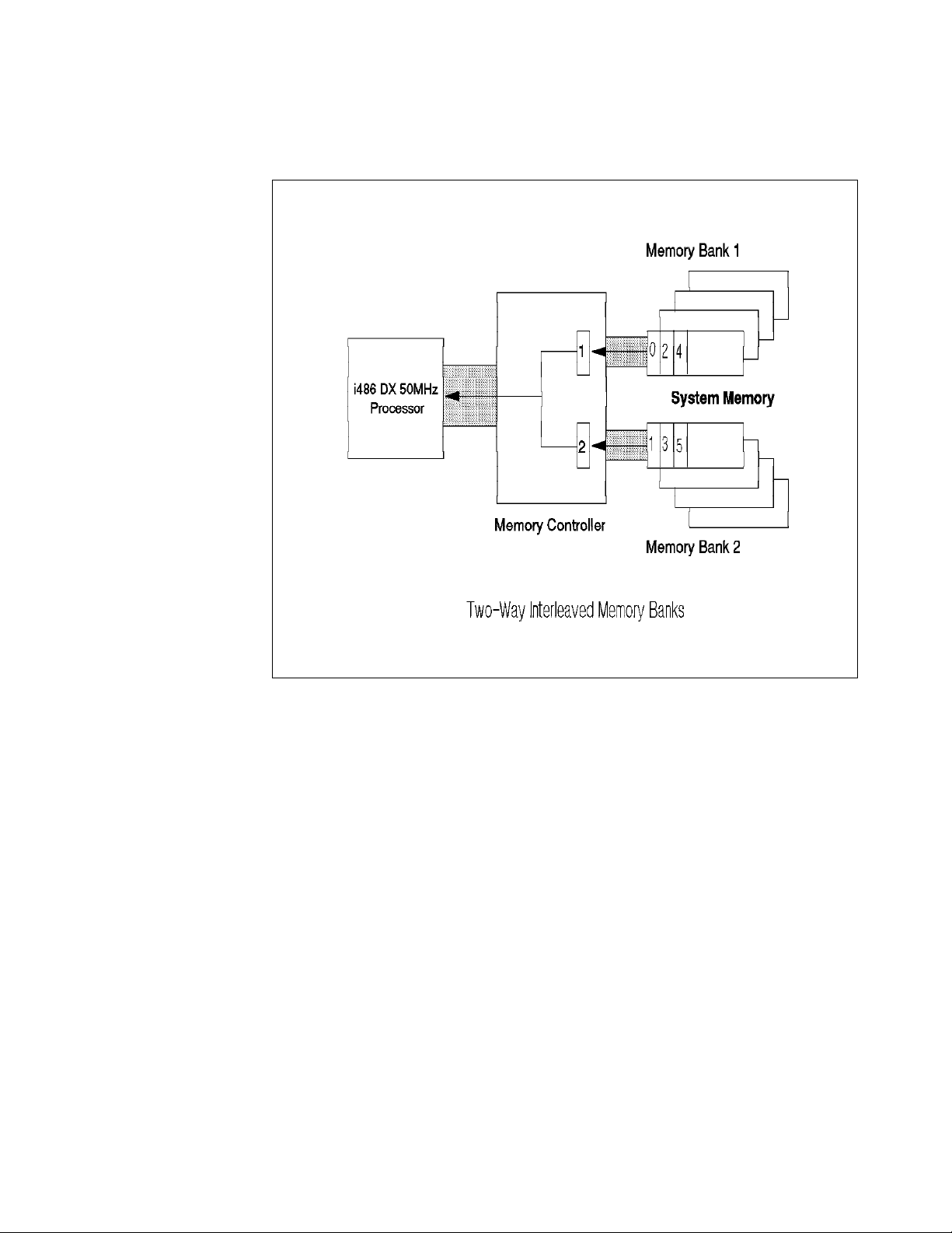
banks. Figure 3 on page 7 shows a two-way interleaved memory
implementation.
Figure 3. Two-Way Interleaved Memory Banks
Memory accesses are overlapped so that as the controller is reading/writing
from bank 1, the address of the next word is presented to bank 2. This gives
bank 2 a head start on the required access time. Similarly, when bank 2 is being
read, bank 1 is fetching/storing the next word.
The PC server 500 uses a two-way interleaved memory. In systems
implementing two-way interleaved memory, additional memory must be added in
pairs of single in-line memory modules (SIMMs) operating at the same speed
(matched SIMMs).
The PC server 720 uses a four-way interleaved memory with a word length of 64
bits. In this system, in order to interleave using 32-bit SIMMs, it is necessary to
add memory in matched sets of eight SIMMs each.
1.3.3 Dual Path Buses
A dual path bus allows both the processor and a bus master to access system
memory simultaneously. Figure 4 on page 8 shows a dual path bus
implementation.
Chapter 1. IBM PC Server Technologies 7
Page 23

┌─────────┐ ┌─────────┐ ┌─────────┐ ┌─────────┐
│ CPU ├───┤ L2 Cache├───┤ Memory ├───┤ Memory │
│ ├───┤ ├───┤ Control.├───┤ │
└─────────┘ └─────────┘ └──┬───┬──┘ └─────────┘
│ │
│ │
┌──┴───┴──┐
│ I/0 │
│ Control.│
└──┬───┬──┘
│ │
│ │
┌──────────────────────────────┴───┴────────────────┐
││
│ BUS ISA/EISA/MCA/VL/PCI │
││
└────┬─┬───┬─┬───────────────────────┬─┬──┬─┬───────┘
││ ││ ││ ││
└─┘ └─┘ └─┘ └─┘
Slots SCSI VGA
Figure 4. Dual Path Bus Implementation
Without a dual path bus, there is often contention for system resources such as
main memory. When contention between the processor and a bus master
occurs, one has to wait for the other to finish its memory cycle before it can
proceed. Thus, fast devices like processors have to wait for much slower I/O
devices, slowing down the performance of the entire system to the speed of the
slowest device. This is very costly to the overall system performance.
1.3.4 SynchroStream Technology
SynchroStream is an extension of the dual bus path technique. The
SynchroStream controller synchronizes the operation of fast and slow devices
and streams data to these devices to ensure that all devices work at their
optimum levels of performance.
It works much like a cache controller in that it pre-fetches extra data on each
access to memory and buffers this data in anticipation of the next request. When
the device requests the data, the IBM SynchroStream controller provides it
quickly from the buffer and the device continues working. It does not have to
wait for a normal memory access cycle.
When devices are writing data into memory, the IBM SynchroStream controller
again buffers the data, and writes it to memory after the bus cycle is complete.
Since devices are not moving data to and from memory directly, but to the
SynchroStream controller, each device has its own logical path to memory. The
devices do not have to wait for other, slower devices.
8 NetWare Integration Guide
Page 24

1.4 Memory Error Detection and Correction
IBM PC servers implement four different memory systems:
•
Standard (parity) memory
•
Error Correcting Code-Parity
•
Error Correcting Code (ECC) memory
•
ECC Memory on SIMMs (EOS) Memory
1.4.1 Standard (Parity) Memory
Parity memory is standard IBM memory with 32 bits of data space and 4 bits of
parity information (one check bit/byte of data). The 4 bits of parity information
are able to tell you an error has occurred but do not have enough information to
locate which bit is in error. In the event of a parity error, the system generates a
non-maskable interrupt (NMI) which halts the system. Double bit errors are
undetected with parity memory.
Standard memory is implemented in the PC Servers 300 and 320 as well as in
the majority of the IBM desktops (for example the IBM PC 300, IBM PC 700, and
PC Power Series 800).
1.4.2 Error Correcting Code (ECC)
The requirements for system memory in PC servers has increased dramatically
over the past few years. Several reasons include the availability of 32 bit
operating systems and the caching of hard disk data on file servers.
As system memory is increased, the possibility for memory errors increase.
Thus, protection against system memory failures becomes increasingly
important. Traditionally, systems which implement only parity memory halt on
single-bit errors, and fail to detect double-bit errors entirely. Clearly, as memory
is increased, better techniques are required.
To combat this problem, the IBM PC servers employ schemes to detect and
correct memory errors. These schemes are called Error Correcting Code (or
sometimes Error Checking and Correcting but more commonly just ECC). ECC
can detect and correct single bit-errors, detect double-bit errors, and detect
some triple-bit errors.
ECC works like parity by generating extra check bits with the data as it is stored
in memory. However, while parity uses only 1 check bit per byte of data, ECC
uses 7 check bits for a 32-bit word and 8 bits for a 64-bit word. These extra
check bits along with a special hardware algorithm allow for single-bit errors to
be detected and corrected in real time as the data is read from memory.
Figure 5 on page 10 shows how the ECC circuits operate. The data is scanned
as it is written to memory. This scan generates a unique 7-bit pattern which
represents the data stored. This pattern is then stored in the 7-bit check space.
Chapter 1. IBM PC Server Technologies 9
Page 25
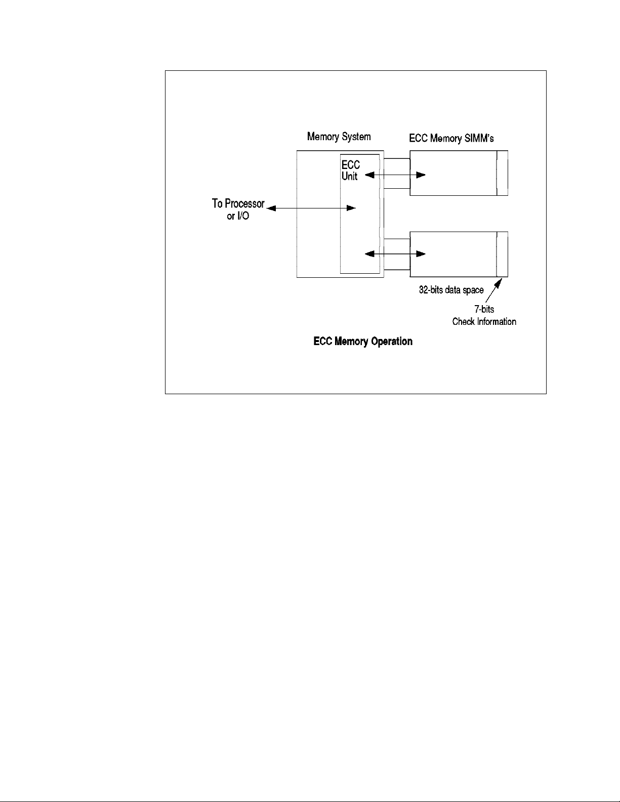
Figure 5. ECC Memory Operation
As the data is read from memory, the ECC circuit again performs a scan and
compares the resulting pattern to the pattern which was stored in the check bits.
If a single-bit error has occurred (the most common form of error), the scan will
always detect it, automatically correct it and record its occurrence. In this case,
system operation will not be affected.
The scan will also detect all double-bit errors, though they are much less
common. With double-bit errors, the ECC unit will detect the error and record its
occurrence in NVRAM; it will then halt the system to avoid data corruption. The
data in NVRAM can then be used to isolate the defective component.
In order to implement an ECC memory system, you need an ECC memory
controller and ECC SIMMs. ECC SIMMs differ from standard memory SIMMs in
that they have additional storage space to hold the check bits.
The IBM PC Servers 500 and 720 have ECC circuitry and provide support for ECC
memory SIMMs to give protection against memory errors.
1.4.3 Error Correcting Code-Parity Memory (ECC-P)
Previous IBM servers such as the IBM Server 85 were able to use standard
memory to implement what is known as ECC-P. ECC-P takes advantage of the
fact that a 64-bit word needs 8 bits of parity in order to detect single-bit errors
(one bit/byte of data). Since it is also possible to use an ECC algorithm on 64
bits of data with 8 check bits, IBM designed a memory controller which
implements the ECC algorithm using the standard memory SIMMs.
10 NetWare Integration Guide
Page 26

Figure 6 on page 11 shows the implementation of ECC-P. When ECC-P is
enabled via the reference diskette, the controller reads/writes two 32-bit words
and 8 bits of check information to standard parity memory. Since 8 check bits
are available on a 64-bit word, the system is able to correct single-bit errors and
detect double-bit errors just like ECC memory.
┌───────────────────┐ ┌───────────────────┐
││││
││││
├─────────┬┬────────┤ ├─────────┬┬────────┤
│ 32 data ││4 parity│ │ 32 data ││4 parity│
└────┬────┘└───┬────┘ └─────┬───┘└────┬───┘
││ ││
│ └───────────────┬──────────┼─────────┘
│││
└─────────────────────┬───┼──────────┘
64 bits for data │ │
│ │8 bits for ECC
┌──┴───┴─────┐
│ Memory │
│ Controller │
└────────────┘
Figure 6. ECC-P Memory Implementation
While ECC-P uses standard non-expensive memory, it needs a specific memory
controller that is able to read/write the two memory blocks and check and
generate the check bits. Also, the additional logic necessary to implement the
ECC circuitry make it slightly slower than true ECC memory. Since the price
difference between a standard memory SIMM and an ECC SIMM has narrowed,
IBM no longer implements ECC-P.
1.4.4 ECC on SIMMs (EOS) Memory
A server that supports one hundred or more users can justify the additional cost
necessary to implement ECC on the system. It is harder to justify this cost for
smaller configurations. It would be desirable for a customer to be able to
upgrade his system at a reasonable cost to take advantage of ECC memory as
his business grows.
The problem is that the ECC and ECC-P techniques previously described use
special memory controllers imbedded on the planar board which contain the
ECC circuits. I t is impossible to upgrade a system employing parity memory
(with a parity memory controller) to ECC even if we upgrade the parity memory
SIMMs to ECC memory SIMMs.
To answer this problem, IBM has introduced a new type of memory SIMM which
has the ECC logic integrated on the SIMM. These are called ECC on SIMMs or
EOS memory SIMMs. With these SIMMs, the memory error is detected and
corrected directly on the SIMM before the data gets to the memory controller.
This solution allows a standard memory controller to be used on the planar
board and allows the customer to upgrade a server to support error checking
memory.
Chapter 1. IBM PC Server Technologies 11
Page 27

1.4.5 Performance Impact
As previously discussed, systems which employ ECC memory have slightly
longer memory access times depending on where the checking is done. It
should be stressed that this affects only the access time of external system
memory, not L1 or L2 caches. Table 1 shows the performance impacts as a
percentage of system memory access times of the different ECC memory
solutions.
Again, these numbers represent only the impact to accessing external memory.
They do not represent the impact to overall system performance which is harder
to measure but will be substantially less.
Table 1. ECC Memory Performances
ECC X X 3% PC Servers 500 and 720
ECC-P X 14% No more (Mod 85)
EOS X None Option for PC Servers
SIMM Memory
Controller
Impact to
Access Time
Systems where
implemented
300, 320
Standard for PC Servers
520
1.4.6 Memory Options and Speed
The following memory options are available from IBM:
•
4MB, 8MB, 16MB, 32MB 70 ns Standard (Parity) Memory SIMMs
•
4MB, 8MB, 16MB, 32MB 70 ns ECC Memory SIMMs
•
4MB, 8MB, 16MB, 32MB 60 ns ECC Memory SIMMs
•
4MB, 8MB, 16MB, 32MB 70 ns EOS Memory SIMMs
Table 2 shows the options used by each PC server.
Table 2. Summary of Memory Implementations
PS/2 Model 70 ns
PC Server
300/310/320
PC Server 500 X
PC Server 520 X
PC Server 720 X
1.5 Bus Architectures
70 ns
Standard
X OPT
ECC-P
70 ns
ECC
60 ns
ECC
70 ns
EOS
There are a number of bus architectures implemented in IBM PC servers:
•
•
•
•
12 NetWare Integration Guide
ISA
EISA
MCA
PCI
Page 28

1.5.1 ISA Bus
The Industry Standard Architecture (ISA) is not really an architecture at all but a
defacto standard based on the original IBM PC/AT bus design. The main
characteristics of the ISA bus include a 16-bit data bus and a 24-bit address bus.
The bus speed is limited to 8 MHz and it did not allow for DMA and bus masters
in its original form. It does not support automatically configuring adapters and
resolving resource conflicts among adapters nor does it allow for sharing of
interrupts. Nonetheless, it was an extremely successful design and even with
these disadvantages, it is estimated that the ISA bus is in 70% of the PCs
manufactured today.
1.5.2 EISA Bus
The Extended Industry Standard Bus Architecture (EISA) is a 32-bit superset of
the ISA bus providing improved functionality and greater data rates while
maintaining backward compatibility with the many ISA products already
available.
The main advancements of the EISA bus are 32-bit addressing and 16-bit data
transfer. It supports DMA and bus master devices. It is synchronized by an 8.33
MHz clock and can achieve data transfer of up to 33 MBps. A bus arbitration
scheme is also provided which allows efficient sharing of multiple EISA bus
devices. EISA systems can also automatically configure adapters.
1.5.3 Micro Channel Bus
The Micro Channel Architecture (MCA) was introduced by IBM in 1987. Micro
Channel is an improvement over ISA in all of the areas discussed in the previous
section on EISA. I n addition, it supports data streaming which is an important
performance feature of the MCA architecture.
1.5.3.1 Data Streaming
The data streaming transfer offers considerably improved I/O performance. In
order to understand data streaming transfers we need to see how data is
transferred between Micro Channel bus master adapters and memory.
The standard method of transfer across the Micro Channel is known as basic
data transfer. In order to transfer a block of data in basic data transfer mode, an
address is generated on the address bus to specify where the data should be
stored; then the data is put on the data bus.
This process is repeated until the entire block of data has been transferred.
Figure 7 on page 14 shows basic data transfer in operation. Basic data transfer
on the Micro Channel runs at 20 MBps (each cycle takes 200 nanoseconds, and
32 bits or 4 bytes of data are transferred at a time).
Chapter 1. IBM PC Server Technologies 13
Page 29
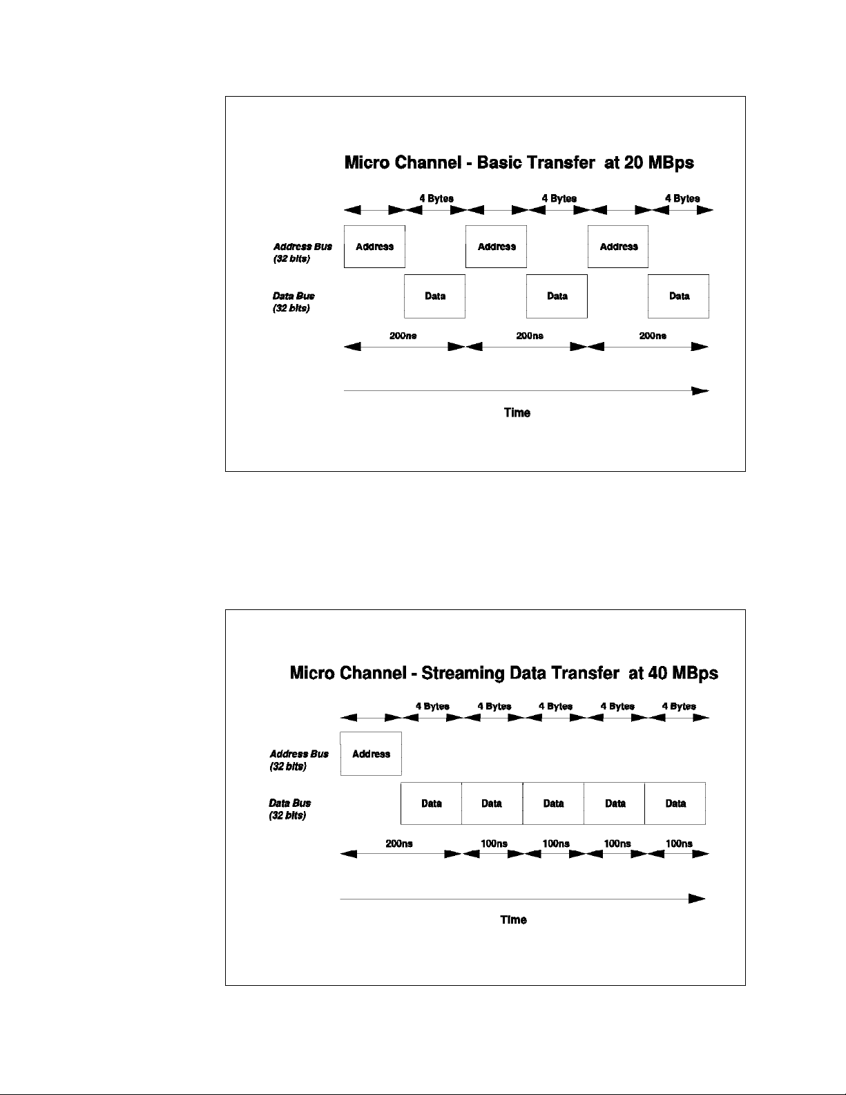
Figure 7. Micro Channel - Basic Data Transfer (20 MBps)
However, in many cases, blocks transferred to and from memory are stored in
sequential addresses, so repeatedly sending the address for each 4 bytes is
unnecessary. With data streaming transfers, the initial address is sent, and then
the blocks of data are sent; it is then assumed that the data requests are
sequential. Figure 8 shows 40 MBps data streaming in operation.
Figure 8. Micro Channel - Data Streaming Transfer (40 MBps)
14 NetWare Integration Guide
Page 30
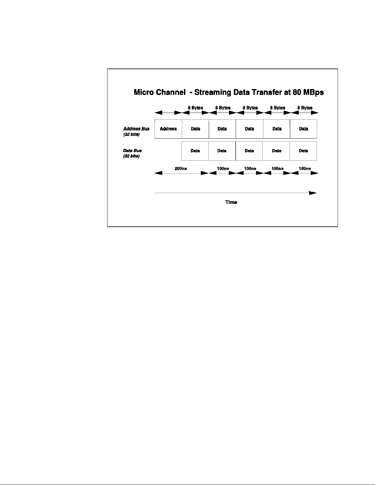
The Micro Channel supports another mode of data streaming whereby the
address bus can also be used to transfer data. This is depicted in Figure 9 on
page 15.
1.5.4 PCI Bus
Figure 9. Micro Channel - Data Streaming Transfer (80 MBps)
As can be seen from this figure, in this mode, after the initial address is
presented during the first bus cycle, the address bus is then multiplexed to carry
an additional 32 bits of data. This results in an effective data transfer rate of 80
MBps.
Data streaming, as well as improving the data transfer rate, also provides a
more efficient use of the Micro Channel. Since MCA operations complete in a
shorter amount of time, the overall throughput of the system is increased.
Data streaming is useful for any adapters that perform block transfers across the
Micro Channel such as the IBM SCSI-2 Fast/Wide Streaming RAID Adapter/A.
MCA is implemented in some models of the IBM PC Server 300 and 500 lines
and in all models of the PC Server 720.
In the later part of 1992, Intel, IBM and a number of other companies worked
together to define a new local component bus which was designed to provide a
number of new features and work with a wide range of new processors. The
result was the Peripheral Component Interconnect (PCI) bus. The PCI bus was
designed to provide the Pentium processor with all the bandwidth it needed and
to provide for more powerful processors in the future. It was also designed for
use in multiprocessing environments.
The PCI bus was designed to work with a number of buses including Micro
Channel, ISA and EISA buses. I t was designed to provide a local bus, more
tightly integrated with the processor, to provide more bandwidth to I/O devices
such as LAN adapters and DISK controllers, which require more bandwidth than
Chapter 1. IBM PC Server Technologies 15
Page 31

is available with previous bus architectures. In order to optimize performance,
the PCI architecture strictly limits the number of loads (hence the number of
adapters) on the bus. It therefore needs an I/O expansion bus to handle the
more routine I/O devices.
The bus has 32 or 64 bits of address and data, is processor independent and is
capable of speeds over 50 MHz. 8-bit and 16-bit devices are not supported. The
64-bit data bus width in combination with clock speeds over 50 MHz can result in
data transfer of several hundred megabytes per second. In addition to memory
space and I/O space, the bus includes a third address space to support
automatic resource allocation and configuration of system and adapter boards.
Unique features of the PCI include parity on all bus lines and control lines. The
parity is not optional as in other architectures, but is required. All PCI bus
masters must support data streaming to memory devices.
1.6 Disk Subsystem
The disk subsystem is a critical element of server design. In this section we
examine the controllers, the devices, and the interfaces between them. We will
specifically address SCSI technology and also examine RAID technology in some
detail.
1.6.1 Hard Disk Interfaces
The disk interface specifies the physical, electrical, and logical connections
between the controller and the Direct Access Storage Devices (DASD). There
have been four main interfaces developed thus far. Each possesses different
characteristics and performance levels. The interfaces are:
1. ST506 - This interface was the original standard for microcomputers. It has a
data transfer rate of 5 million bits per second (Mbps) between the controller
and the DASD Device. It is a serial rather than a parallel interface. This
interface is classified as a device level interface because the device itself
has no logic to interpret commands. Functions such as formatting, head
selection, and error detection are directed by the controller which is housed
in an adapter card. A device level interface requires specific adapters and
device drivers for each different type of device.
2. Enhanced Small Device Interface (ESDI) - This is an enhanced version of the
ST506 interface. I t provides a 10 Mbps data transfer rate (15 Mbps in some
implementations). ESDI devices were the first to use a type of data encoding
called Run Length Limited (RLL) which results in denser storage and faster
data transfer than the older modified frequency modulation (MFM) technique.
However, it is still a device level, serial interface.
3. Integrated Drive Electronics (IDE) - This is a bus level interface meaning that
the device controller is built into the device itself. The IDE interface was
designed for the low cost PC market segment. The interface is flexible and
has been enhanced over time. The latest enhancements include caching at
the adapter level, a CD-ROM interface, and an extension of the maximum
disk storage which was previously limited to 500 MB. However, most IDE
implementations still limit the maximum number of hard disks per interface
to two. This limitation makes IDE more applicable for desktop systems.
16 NetWare Integration Guide
Page 32

4. Small Computer System Interface (SCSI) - The SCSI interface is a high speed
parallel interface that transfers eight bits at a time rather than one bit at a
time for the ST506 and ESDI serial interfaces. Thus data transfer rates for
SCSI are measured in mega
faster than those of the serial interfaces. SCSI is also a bus level interface
which makes it very flexible. Since the commands are interpreted by the
device and not the SCSI host bus adapter, new devices (with new
commands) can be implemented and used with standard SCSI adapters. The
device driver then interacts with the device via the new commands. A n
example of this would be a CD-ROM device sharing the same adapter as a
hard disk drive. Figure 10 shows a SCSI subsystem with a host bus adapter
attached to an integrated controller and hard disk.
bytes
versus mega
bits
and are considerably
Figure 10. SCSI Disk Interface
The SCSI flexibility and high performance make it very suitable for the server
environment. In fact, SCSI is the most widely used disk subsystem
technology in advanced servers today. All the current IBM PC Servers
except for a few at the low end use this technology. For these reasons, we
will take a closer look at this interface.
1.6.2 SCSI Technology
As previously discussed, SCSI is a bus level interface through which computers
may communicate with a large number of devices of different types connected to
the system unit via a SCSI controller and daisy-chained cable. The attached
devices include such peripherals as fixed disks, CD-ROMs, printers, plotters, and
scanners. The SCSI controller may be in the form of an adapter or integrated on
the planar board.
There are several terms and concepts used in discussing SCSI technology that
require definition.
•
SCSI-I and SCSI-II:
SCSI is a standard defined by the American National Standards Institute
(ANSI). The original SCSI-I standard is defined in ANSI standard X3.131-1986.
Chapter 1. IBM PC Server Technologies 17
Page 33

It defines an 8-bit interface with a data transfer rate of 5 MBps. SCSI-II is the
second SCSI standard and is defined in ANSI standard X3T9.2/375R REV10K.
It defines extensions to SCSI-I which allow for 16 and 32-bit devices, a 10
MBps transfer rate, and other enhancements discussed below.
•
Common Command Set
The SCSI standard defines a set of commands which must be interpreted by
all devices that attach to a SCSI bus. This is called the common command
set. Unique devices may implement their own commands, which can be sent
by a device driver and interpreted by the device. The advantage of this
architecture is that the SCSI adapter does not have to change when new
devices with new capabilities are introduced.
•
Tagged Command Queuing (TCQ)
TCQ is a SCSI-II enhancement. I t increases performance in DASD intensive
server environments. With SCSI-I systems, only two commands could be
sent to a fixed disk; the disk would store one while operating on the other.
With TCQ it is possible to send multiple commands to the fixed disk and the
disk stores the commands and executes each command in the sequence that
gives optimal performance.
•
Scatter/Gather
Scatter/Gather allows devices to transfer data to and from non-contiguous or
scattered
areas of system memory and on-board cache independently of the
CPU. This, again, increases CPU overlap. The Scatter/Gather feature allows
for high performance, even in systems that have fragmented memory buffers.
•
Fast/Wide Devices and Controllers
Fast
refers to the doubling of the data transfer rate from the SCSI-I 5 MBps to
Wide
10 MBps.
is used in reference to the width of the SCSI parallel bus
between the adapter and the device. Wide generically means wider than the
original 8-bit path defined in SCSI-I. Its use is currently limited to mean
16-bits as 32-bit implementations are not currently available. With a 16-bit
path, the data rate is double that of an 8-bit device.
Fast/Wide
refers to
adapters and devices which implement both the fast and wide interfaces
defined above. A fast/wide device has a maximum data transfer rate of 20
MBps.
Note
Wide refers to the width of the bus between the SCSI adapter and the
disk drive or other SCSI device. Do not get this confused with the width
of the host bus interface (for example, a 32-bit MCA or PCI adapter).
•
18 NetWare Integration Guide
Disconnect/Reconnect
Some commands take a relatively long time to complete (for example a seek
command which takes roughly 11 ms). With this feature, the controller can
disconnect from the bus while the device is positioning the heads (seeking).
Then, when the seek is complete and data is ready to be transferred, the
device can arbitrate for the bus and then reconnect with the controller to
transfer the data. This allows a much more efficient use of the available
Page 34

SCSI bus bandwidth. If the controller held onto the bus while waiting for the
device to seek, then the other devices would be locked out. This is also
sometimes referred to as overlapped operations or multi-threaded I/O on the
SCSI bus. This feature is very important in multitasking environments.
•
Synchronous versus Asynchronous
An asynchronous device must acknowledge each byte as it comes from the
controller. Synchronous devices may transfer data in bursts and the
acknowledgments happen after the fact. The latter is much faster than the
former and most newer devices support this mode of operation. The
adapters negotiate with devices on the SCSI bus to ensure that the mode
and data transfer rates are acceptable to both the host adapter and the
devices. This process prevents data from being lost and ensures that data
transmission is error free.
1.6.3 SCSI Adapters
The SCSI adapter provides the interface between the host bus (for example
Micro Channel or PCI) and the SCSI bus. The SCSI adapters that IBM has
developed are:
•
IBM Personal System/2 Micro Channel SCSI Adapter
This adapter is a 16-bit Micro Channel bus master adapter adhering to the
SCSI-I interface. It is capable of an 8.3 MBps burst data transfer rate on the
Micro Channel. It uses a 16-bit data path and can use a 24- or a 32-bit
address on the Micro Channel. It can be installed in either a 16- or 32-bit
MCA slot, but if the system has more than 16MB of memory, it must be put in
a 32-bit slot due to the limitations of 24-bit addressing in a 16-bit slot.
The bus master capability of this SCSI adapter optimizes data flow from each
SCSI device configured to the system. This capability can provide
performance benefits in applications where multitasking or high-speed data
flow is essential. It allows the processor to be off-loaded from many of the
input/output activities common to DASD transfers. This adapter also
conforms to the Subsystem Control Block (SCB) architecture for Micro
Channel bus masters.
•
IBM Personal System/2 Micro Channel SCSI Adapter with Cache
This adapter provides a superset of the features of the PS/2 Micro Channel
SCSI Adapter. It is a 32-bit Micro Channel bus master adapter containing a
512KB cache buffer. The cache is used to buffer data between system
memory and the device, which permits higher efficiency on both the Micro
Channel and the SCSI buses. It has a burst data transfer rate on the Micro
Channel of 16.6 MBps. This adapter is recommended where improved data
transfer rates and multiple SCSI devices are required and system memory is
constrained.
•
IBM SCSI-2 Fast/Wide Adapter/A
This adapter is a high performance SCSI-II adapter and a 32-bit Micro
Channel bus master adapter capable of streaming data at 40 MBps. It has
dual SCSI-II fast and wide channels (one 20 MBps internal and one 20 MBps
external). It supports devices using either asynchronous, synchronous, or
fast synchronous (10 MBps) SCSI data transfer rates. It also supports
Chapter 1. IBM PC Server Technologies 19
Page 35

standard 8-bit SCSI devices. Up to seven SCSI physical devices may be
attached to this adapter.
This adapter has a dedicated 80C186 local processor on board, which allows
it to implement advanced features such as TCQ.
The dual bus design of the adapter prevents access to internal DASD from
the external port. It also allows the maximum cable length to be calculated
individually for each bus. This allows for additional capability externally.
•
IBM SCSI-2 Fast/Wide Streaming-RAID Adapter/A
This adapter has the same performance advantages of the IBM SCSI-2
Fast/Wide Streaming Adapter/A plus a RAID array controller. This feature
offers the additional data protection security inherent in RAID configurations.
Also, the adapter microcode is optimized for database and video server
environments.
Two independent SCSI buses are available for internal and external array
configurations, further enhancing performance and fault tolerant
configurations. The dual bus of the adapter allows for a maximum
connection of up to 14 drives, seven on each individual bus. One bus cannot
support internal and external devices simultaneously.
•
IBM SCSI-2 Fast PCI Adapter
This adapter features a RISC processor which reduces the time the adapter
needs to process SCSI commands. It also supports system DMA which
reduces the CPU overhead by transferring data into the system memory
directly.
It contains two SCSI-II ports, one internal and one external, and supports up
to seven SCSI-II fast devices at a 10 MBps data transfer rate. I t implements
advanced features such as:
− Multi-thread I/O
− Scatter/Gather
− Tagged Command Queueing
− Synchronous and asynchronous Fast SCSI modes
•
IBM SCSI-2 Fast/Wide PCI Adapter
In addition to the features supported with the IBM SCSI-2 Fast PCI Adapter
characteristics, the IBM SCSI-2 Fast/Wide Adapter provides a 20 MBps data
transfer rate.
It contains three SCSI-II ports:
− One 50-pin 8-bit internal connector
− One 68-pin 16-bit wide internal connector
•
20 NetWare Integration Guide
− One 68-pin 16-bit wide external connector
It can support up to 15 units, on two of the three ports. If you connect
external devices to the adapter, you can attach internal SCSI devices to one
or the other,
but not to both
internal SCSI connectors.
IBM SCSI-2 Fast/Wide RAID PCI Adapter
Page 36

In addition to the features supported with the IBM SCSI-2 F/W PCI Adapter,
the IBM SCSI-2 F/W RAID adapter provides a RAID controller. Please
reference 1.6.5, “RAID Technology” on page 22 for a discussion on RAID.
1.6.3.1 Summary
The following tables summarize the features of the IBM SCSI adapters.
Table 3. SCSI Adapters Summary
Attribute SCSI Adapter
with no Cache
SCSI Bus Width 16-bit 32-bit 32-bit 32-bit
SCSI Data Transfer Rate 5 MBps 5 MBps 20 MBps 20 MBps
Micro Channel Data Transfer Rate 8.3 MBps 16.6 MBps 20 MBps 40/80 MBps
Parity Optional Optional Yes Yes
Tagged Command Queueing
(TCQ)
Systems where implemented 500 500/720
Note: Fast and Wide are data transfer methods as defined in SCSI-II.
The 720 will support 80 MBps data streaming with the SCSI-2 Fast/Wide Streaming RAID Adapter/A
N/A = not available
N/A N/A Yes Yes
Enhanced
SCSI Adapter
with Cache
SCSI-2
Fast/Wide
Adapter/A
SCSI-2
Fast/Wide
Streaming
RAID
Adapter/A
Table 4. PCI SCSI Adapters Summary
Attribute PCI SCSI-2 Fast
Adapter
SCSI Bus Width 32-bit 32-bit 32-bit
SCSI Data Transfer Rate 10 MBps 20 MBps 20 MBps
Parity Yes Yes Yes
Tagged Command Queueing (TCQ) Yes Yes Yes
Systems where implemented PC Server 300/310 PC Server 320/520 PC Server 320/520
Note: Fast and Wide are data transfer methods as defined in SCSI-II
PCI SCSI-2
Fast/Wide Adapter
PCI SCSI-2
Fast/Wide RAID
Adapter
1.6.4 Hard Disk Drives
Ultimately, the hard disk drive is the component that has the most effect on
subsystem performance. The following specs should be considered when
evaluating hard disks in order to optimize performance:
•
Average access time
•
Maximum transfer rate
•
On-board cache size
Average access time is one of the standard indicators of hard drive performance.
This is the amount of time required for the drive to deliver data after the
computer sends a read request. It is composed of two factors, the seek time and
the rotational delay. The seek time is the time necessary to position the heads
Chapter 1. IBM PC Server Technologies 21
Page 37

to the desired cylinder of the disk. The latency is the amount of time it takes for
the disk to rotate to the proper sector on that cylinder.
It should be noted that two disks of the same physical size, for example 3.5-inch
disks, will differ in their access times with the larger capacity disk having a
better access time. This is due to the fact that the distance between cylinders is
shorter on the larger disk and, therefore, seek time is reduced. This is the
primary reason that disk access times have been reduced as capacities have
been increased.
Maximum transfer rate is the rate at which the device can deliver data back to
the SCSI adapter. I t mainly depends on the processor/DMA controller integrated
on the device but can be no more than the SCSI maximum data transfer rate, for
example 20 MBps for a SCSI-II Fast/Wide interface.
Caching is important for the same reason it is important on other subsystems;
namely, it speeds up the time it takes to perform routine operations. For high
performance, the drive should be able to provide write caching. With write
caching, the drive signals the completion of the write immediately after it
receives the data but before the data is actually written to disk. The system then
continues to do other work while the hard disk is actually writing the data.
Performance is significantly better because subsequent disk operations can be
overlapped with this cached write operation.
The following table summarizes the specifications on current IBM PC Server
hard disks:
Table 5. Summary of Disks Performance Characteristics
Disk Average
Seek
Time
1GB Fast 8.6 ms 10 MBps 3.7-4.5 MBps 5.56 ms 500
2GB Fast 9.5 ms 10 MBps 3.7-4.5 MBps 5.56 ms 500
1.08GB Fast 10.5 ms 10 MBps 3.2-4.0 MBps 5.56 ms 500
1.12GB F/W 6.9 ms 20 MBps 5.5-7.4 MBps 4.17 ms 1000
2.25GB F/W 7.5 ms 20 MBps 5.5-7.4 MBps 4.17 ms 1000
4.51GB F/W 8.0 ms 20 MBps 5.5-7.4 MBps 4.17 ms 1000
Burst
Transfer
Rate
Sustained
Transfer
Rate
Average
Latency
(K hours)
1.6.5 RAID Technology
Several factors have contributed to the growing popularity of disk arrays:
•
Performance
The capacity of single large disks has grown rapidly, but the performance
improvements have been modest, when compared to the advances made in
the other subsystems that make up a computer system. The reason for this
is that disks are mechanical devices, affected by delays in positioning
read/write heads (seeks) and the rotation time of the media (Latency).
MTBF
•
22 NetWare Integration Guide
Reliability
Page 38

Disks are often among the least reliable components of the computer
systems, yet the failure of a disk can result in the unrecoverable loss of vital
business data, or at the very least a need to restore from tape with
consequent delays.
•
Cost
It is cheaper to provide a given storage capacity and a given performance
level with several small disks connected together than with a single disk.
There is nothing unusual about connecting several disks to a computer to
increase the amount of storage. Mainframes and minicomputers have always
had banks of disks. It becomes a disk array when several disks are connected
and accessed by the disk controller in a predetermined pattern designed to
optimize performance and/or reliability.
Disk arrays seem to have been invented independently by a variety of groups,
but it was the Computer Architecture Group at the University of California,
Berkeley who invented the term RAID. RAID stands for
Inexpensive Disks
and provides a method of classifying the different ways of
using multiple disks to increase availability and performance.
Redundant Array of
1.6.6 RAID Classifications
The original RAID classification described five levels of RAID (RAID-1 through 5).
RAID-0 (data-striping) and RAID-1 Enhanced (data stripe mirroring) have been
added since the original levels were defined. RAID-0 is not a pure RAID type,
since it does not provide any redundancy.
Different designs of arrays perform optimally in different environments. The two
main environments are those where high transfer rates are very important, and
those where a high I/O rate is needed, that is, applications requesting short
length random records.
Table 6 shows the RAID array classifications, and is followed by brief
descriptions of their designs and capabilities.
Table 6. RAID Classifications
RAID Level Description
RAID-0 Block Interleave Data Striping without Parity
RAID-1 Disk Mirroring/Duplexing
RAID-1 (Enhanced) Data Stripe Mirroring
RAID-2 Bit Interleave Data Striping with Hamming Code
RAID-3 Bit Interleave Data Striping with Parity Disk
RAID-4 Block Interleave Data Striping with one Parity Disk
RAID-5 Block Interleave Data Striping with Skewed Parity
Chapter 1. IBM PC Server Technologies 23
Page 39

1.6.6.1 RAID-0 - Block Interleave Data Striping without Parity
Striping of data across multiple disk drives without parity protection is a disk
data organization technique sometimes employed to maximize DASD subsystem
performance (for example, Novell NetWare′s
data scatter
option).
An additional benefit of this data organization is
striped across multiple drives in an array, the logical drive size is the sum of the
individual drive capacities. The maximum file size may be limited by the
operating system.
│
┌───────┴───────┐
│ Disk │
│ Controller │
└───────┬───────┘
│
│
┌─────────────┬────────────┼────────────┬────────────┐
│ │ │ │ │
┌────┴─────┐ ┌────┴─────┐ ┌────┴─────┐ ┌────┴─────┐ ┌────┴─────┐
│ xxxxx │ │ xxxxx │ │ xxxxx │ │ xxxxx │ │ xxxxx │ Block 0
├──────────┤ ├──────────┤ ├──────────┤ ├──────────┤ ├──────────┤
│ yyyyy │ │ zzzzz │ │ │ │ │ │ │
├──────────┤ ├──────────┤ ├──────────┤ ├──────────┤ ├──────────┤
│ │ │ │ │ │ │ │ │ │ Block n
└──────────┘ └──────────┘ └──────────┘ └──────────┘ └──────────┘
Disk 1 Disk 2 Disk 3 Disk 4 Disk 5
xxxxx = Blocks belonging to a long file
yyyyy and zzzzz = Blocks belonging to short files
drive spanning
. With data
Figure 11. RAID-0 (Block Interleave Data Striping without Parity)
Data striping improves the performance with large files since reads/writes are
overlapped across all disks. However, reliability is decreased as the failure of
one disk will result in a complete failure of the disk subsystem according to the
formula:
Mean Time to Failure of a single disk
Mean Time to Failure = ─────────────────────────────────────
Number of Disks in the array
1.6.6.2 RAID-1 - Disk Mirroring/Duplexing
This approach keeps two complete copies of all data. Whenever the system
makes an update to a disk, it duplicates that update to a second disk, thus
mirroring the original. Either disk can fail, and the data is still accessible.
Additionally, because there are two disks, a read request can be satisfied from
either device, thus leading to improved performance and throughput. Some
implementations optimize this by keeping the two disks 180 degrees out of phase
with each other, thus minimizing latency.
However, mirroring is an expensive way of providing protection against data
loss, because it doubles the amount of disk storage needed (as only 50% of the
installed disk capacity is available for data storage).
24 NetWare Integration Guide
Page 40

┌───────────────────┐
││
│ ┌───────────┤
│ │ Disk ├───────────────┬────┬───────────┐
│ │ Controller│ │ │ Disk 1 │
│ └───────────┤ │ └───────────┘
│││
│ │ └────┬───────────┐
│ │ │ Disk 2 │
│ │ └───────────┘
││
││
││
└───────────────────┘
Figure 12. RAID-1 (Disk Mirroring)
Disk mirroring involves duplicating the data from one disk onto a second disk
using a single controller.
Disk duplexing is the same as mirroring in all respects, except that the disks are
attached to separate controllers. The server can now tolerate the loss of one
disk controller, as well as or instead of a disk, without loss of the disk
subsystem′s availability or the customer′s data. Since each disk is attached to a
separate controller, performance and throughput may be further improved.
┌───────────────────┐
││
│ ┌───────────┤
│ │ Disk ├────────────────────┬───────────┐
│ │ Controller│ │ Disk 1 │
│ └───────────┤ └───────────┘
││
│ ┌───────────┤
│ │ Disk ├────────────────────┬───────────┐
│ │ Controller│ │ Disk 2 │
│ └───────────┤ └───────────┘
││
││
└───────────────────┘
Figure 13. RAID-1 (Disk Duplexing)
1.6.6.3 RAID-1 Enhanced - Data Strip Mirroring
RAID level 1 supported by the IBM PC Server array models provides an
enhanced feature for disk mirroring that stripes data and copies of the data
across all the drives of the array. The first stripe is the data stripe; the second
stripe is the mirror (copy) of the first data stripe, but, it is shifted over one drive.
Because the data is mirrored, the capacity of the logical drive, when assigned to
RAID 1 Enhanced, is 50 percent of the physical capacity of the hard disk drives in
the array.
Chapter 1. IBM PC Server Technologies 25
Page 41

│
┌───────┴───────┐
│ Disk │
│ Controller │
└───────┬───────┘
│
│
┌────────────┼────────────┐
│ │ │
┌────┴─────┐ ┌────┴─────┐ ┌────┴─────┐
DATA │ AAA │ │ BBB │ │ CCC │
├──────────┤ ├──────────┤ ├──────────┤
DATA MIRROR │ CCC │ │ AAA │ │ BBB │
├──────────┤ ├──────────┤ ├──────────┤
DATA │ DDD │ │ EEE │ │ FFF │
├──────────┤ ├──────────┤ ├──────────┤
DATA MIRROR │ FFF │ │ DDD │ │ EEE │
└──────────┘ └──────────┘ └──────────┘
Disk 1 Disk 2 Disk 3
Figure 14. RAID-1 Enhanced, Data Strip Mirroring
Some vendors have also implemented another slight variation of RAID-1 and
refer to it as RAID-10 since it combines features of RAID-1 and RAID-0. Others
refer to this technique as RAID-6, which is the next available RAID level.
As shown in Figure 15, this solution consists of mirroring a striped (RAID-0)
configuration. In this example, a RAID-0 configuration consisting of 2 drives
(drive 1 and 2) is mirrored to drives 3 and 4.
│
┌───────┴───────┐
│ Disk │
│ Controller │
└───────┬───────┘
│
│
┌────────────┬──────┴─────┬────────────┐
│ │ │ │
┌────┴─────┐ ┌────┴─────┐ ┌────┴─────┐ ┌────┴─────┐
│ AAA │ │ BBB │ │ AAA │ │ BBB │
├──────────┤ ├──────────┤ ├──────────┤ ├──────────┤
│ CCC │ │ DDD │ │ CCC │ │ DDD │
├──────────┤ ├──────────┤ ├──────────┤ ├──────────┤
│ EEE │ │ FFF │ │ EEE │ │ FFF │
├──────────┤ ├──────────┤ ├──────────┤ ├──────────┤
│ GGG │ │ HHH │ │ GGG │ │ HHH │
└──────────┘ └──────────┘ └──────────┘ └──────────┘
Disk 1 Disk 2 Disk 3 Disk 4
Figure 15. RAID-6,10 - Mirroring of RAID 0 Drives
Performance and capacity are similar to RAID 1. 50% of total disk capacity is
usable. However, this solution always uses an
enhanced can use an
others RAID levels.
26 NetWare Integration Guide
even
odd
number of disks. RAID-1 also can be mixed with
number of disks. RAID-1
Page 42

1.6.6.4 RAID-2 - Bit Interleave Data Striping with Hamming Code
This type of array design is another form of data striping: it spreads the data
across the disks one bit or one byte at a time in parallel. This is called bit (or
byte) interleaving.
Thus, if there were five disks in the array, a sector on the first drive will contain
bits 0 and 5, and so on of the data block; the same sector of the second drive
will contain bits 1 and 6, and so on as shown in Figure 16.
RAID-2 improves on the 50% disk overhead in RAID-1 but still provides
redundancy by using the Hamming code. This is the same algorithm used in
ECC memory. The check bits can be generated on a nibble (4 bits), a byte (8
bits), a half word (16 bits) or a word (32 bits) basis but the technique works most
efficiently with 32-bit words. Just like with ECC, it takes 7 check bits to
implement the Hamming code on 32 bits of data.
Generating check bits by byte is probably the process used most frequently. For
example, if data were grouped into bytes, 11 drives in total would be required, 8
for data and 3 for the check bits. An 8-3 configuration reduces the overhead to
27%.
Note: For clarity, the Hamming Code drives are not shown in Figure 16.
An array of this design will perform optimally when large data transfers are
being performed. The host will see the array as one logical drive. The data
transfer rate, however, will be the product of the number of drives in the array
and the transfer rate of the individual drives.
This design is unable to handle multiple, simultaneous small requests for data,
unlike the previous design; so, it is unlikely to satisfy the requirements for a
transaction processing system that needs a high transaction rate.
│
┌───────┴───────┐
│ Disk │
│ Controller │
└───────┬───────┘
│
│
┌─────────────┬────────────┼────────────┬────────────┐
│ │ │ │ │
┌────┴─────┐ ┌────┴─────┐ ┌────┴─────┐ ┌────┴─────┐ ┌────┴─────┐
│ Bit 0 │ │ Bit 1 │ │ Bit 2 │ │ Bit 3 │ │ Bit 4 │
├──────────┤ ├──────────┤ ├──────────┤ ├──────────┤ ├──────────┤
│ Bit 5 │ │ Bit 6 │ │ Bit 7 │ │ Bit 8 │ │ Bit 9 │
├──────────┤ ├──────────┤ ├──────────┤ ├──────────┤ ├──────────┤
│ Bit 10 │ │ Bit 11 │ │ Bit 12 │ │ Bit 13 │ │ Bit 14 │
└──────────┘ └──────────┘ └──────────┘ └──────────┘ └──────────┘
Disk 1 Disk 2 Disk 3 Disk 4 Disk 5
Figure 16. RAID-2 (Bit Interleave Data Striping with Hamming Code)
Chapter 1. IBM PC Server Technologies 27
Page 43

1.6.6.5 RAID-3 - Bit Interleave Data Striping with Parity Disk
The use of additional disks to redundantly encode customer′s data and guard
against loss is referred to as check sum, disk parity or error correction code
(ECC). The principle is the same as memory parity, where the data is guarded
against the loss of a single bit.
Figure 17 shows an example of RAID-3. Four of the disks hold data, and can be
accessed independently by the processor, while the fifth is hidden from the
processor and stores the parity of the other four. Writing data to any of the disks
(1, 2, 3 or 4) causes the parity to be recomputed and written to disk 5. If any of
the data disks subsequently fail, the data can still be accessed by using the
information from the other data disks along with the parity disk which is used to
reconstruct the data on the failed disk.
Since the files are held on individually addressable disks, this design offers a
high I/O rate. Compared to a single disk of similar capacity, this array has more
actuators for the same amount of storage. These actuators will work in parallel,
as opposed to the sequential operation of the single actuator, thus reducing
average access times.
│
┌───────┴───────┐
│ Disk │
│ Controller │
└───────┬───────┘
│
│
┌─────────────┬────────────┼────────────┬────────────┐
│ │ │ │ │
┌────┴─────┐ ┌────┴─────┐ ┌────┴─────┐ ┌────┴─────┐ ┌────┴─────┐
│ Bit 0 │ │ Bit 1 │ │ Bit 2 │ │ Bit 3 │ │ Parity │
├──────────┤ ├──────────┤ ├──────────┤ ├──────────┤ ├──────────┤
│ Bit 4 │ │ Bit 5 │ │ Bit 6 │ │ Bit 7 │ │ Parity │
├──────────┤ ├──────────┤ ├──────────┤ ├──────────┤ ├──────────┤
│ │ │ │ │ │ │ │ │ Parity │
└──────────┘ └──────────┘ └──────────┘ └──────────┘ └──────────┘
Disk 1 Disk 2 Disk 3 Disk 4 Disk 5
Figure 17. RAID-3 (Bit Interleave Data Striping with Parity Disk)
Multiple disks are used with the data scattered across them. One disk is used
for parity checking for increased fault tolerance.
1.6.6.6 RAID-4 - Block Interleave Data Striping with One Parity Disk
The performance of bit-interleaved arrays in a transaction processing
environment, where small records are being simultaneously read and written, is
very poor. This can be compensated for by altering the striping technique, such
that files are striped in block sizes that correspond to the record size being read.
This will vary in different environments. Super-computer type applications may
require a block size of 64KB, while 4KB will suffice for most DOS applications.
28 NetWare Integration Guide
Page 44

┌─────────────┬────────────┼────────────┬────────────┐
│ │ │ │ │
┌────┴─────┐ ┌────┴─────┐ ┌────┴─────┐ ┌────┴─────┐ ┌────┴─────┐
│ xxxxx │ │ xxxxx │ │ xxxxx │ │ xxxxx │ │ Parity │ Block 0
├──────────┤ ├──────────┤ ├──────────┤ ├──────────┤ ├──────────┤
│ yyyyy │ │ yyyyy │ │ yyyyy │ │ yyyyy │ │ Parity │
├──────────┤ ├──────────┤ ├──────────┤ ├──────────┤ ├──────────┤
│ │ │ │ │ │ │ │ │ │ Block n
└──────────┘ └──────────┘ └──────────┘ └──────────┘ └──────────┘
Disk 1 Disk 2 Disk 3 Disk 4 Disk 5
xxxxx and yyyyy = Blocks belonging to long files
Figure 18. RAID-4 (Block Interleave Data Striping with One Parity Disk)
│
┌───────┴───────┐
│ Disk │
│ Controller │
└───────┬───────┘
│
│
1.6.6.7 RAID-5 - Block Interleave Data Striping with Skewed Parity
The RAID-5 design tries to overcome all of these problems. Data is striped
across the disks to ensure maximum read performance when accessing large
files, and having the data striped in blocks improves the array′s performance in
a transaction processing environment. Parity information is stored on the array
to guard against data loss. Skewing is used to remove the bottleneck that is
created by storing all the parity information on a single drive.
│
┌───────┴───────┐
│ Disk │
│ Controller │
└───────┬───────┘
│
│
┌─────────────┬────────────┼────────────┬────────────┐
│ │ │ │ │
┌────┴─────┐ ┌────┴─────┐ ┌────┴─────┐ ┌────┴─────┐ ┌────┴─────┐
│ xxxxx │ │ xxxxx │ │ xxxxx │ │ xxxxx │ │ Parity │ Block 0
├──────────┤ ├──────────┤ ├──────────┤ ├──────────┤ ├──────────┤
│ xxxxx │ │ xxxxx │ │ xxxxx │ │ Parity │ │ xxxxx │
├──────────┤ ├──────────┤ ├──────────┤ ├──────────┤ ├──────────┤
│ yyyyy │ │ yyyyy │ │ Parity │ │ yyyyy │ │ yyyyy │
├──────────┤ ├──────────┤ ├──────────┤ ├──────────┤ ├──────────┤
│ │ │ │ │ │ │ │ │ │ Block n
└──────────┘ └──────────┘ └──────────┘ └──────────┘ └──────────┘
Disk 1 Disk 2 Disk 3 Disk 4 Disk 5
xxxxx and yyyyy = Blocks belonging to long files
Figure 19. RAID-5 (Block Interleave Data Striping with Skewed Parity)
Chapter 1. IBM PC Server Technologies 29
Page 45

1.6.6.8 Summary of RAID Performance Characteristics
RAID-0:
•
•
•
Block Interleave Data Striping without parity
Fastest data-rate performance
Allows seek and drive latency to be performed in parallel
Significantly outperforms single large disk
RAID-1:
Disk Mirroring/Disk Duplexing and Data Strip mirroring (RAID-1,
Enhanced)
•
Fast and reliable, but requires 100% disk space overhead
•
Data copied to each set of drives
•
No performance degradation with a single disk failure
•
RAID-1 enhanced provides mirroring with an odd number of drives
RAID-2:
•
•
RAID-3:
•
•
•
•
•
Bit Interleave Data Striping with Hamming Code
Very fast for sequential applications, such as graphics modelling
Almost never used with PC-based systems
Bit Interleave Data Striping with Parity
Access to all drives to retrieve one record
Best for large sequential reads
Very poor for random transactions
Poor for any write operations
Faster than a single drive, but much slower than RAID-0 or RAID-1 in random
environments
RAID-4:
•
•
•
Block Interleave Data Striping with one Parity Disk
Best for large sequential I/O
Very poor write performance
Faster than a single drive, but usually much slower than RAID-0 or RAID-1
RAID-5:
•
•
•
•
•
Block Interleave Data Striping with Skewed Parity
Best for random transactions
Poor for large sequential reads if request is larger than block size
Better write performance than RAID-3 and RAID-4
Block size is key to performance, must be larger than typical request size
Performance degrades in recovery mode (when a single drive has failed)
Table 7. Summary of RAID Performance Characteristics
RAID Level Capacity Large Transfers High I/O Rate Data Availability
Single Disk Fixed (100%) Good Good 1
RAID-0 Excellent Very Good Very Good Poor 2
RAID-1 Moderate (50%) Good Good Good
RAID-2 Very Good Good Poor Good
RAID-3 Very Good Very Good Poor Good
RAID-4 Very Good Very Good Poor Good
RAID-5 Very Good Very Good Good Good
Note:
1The MTBF (mean time before failure) for single disks can range from 10,000 to 1,000,000 hours.
2Availability = MTBF of one disk divided by the number of disks in the array.
30 NetWare Integration Guide
Page 46

1.6.7 Recommendations
•
Use IDE on smaller systems
IDE actually outperforms SCSI on systems where only one or two devices are
attached. Several models of the IBM PC Server 300 and 320 lines implement
IDE as an integrated controller on the planar board. This is more than
adequate if no more than a couple of hard disks will be used.
•
Distribute the workload on large systems
Research has shown that a single 66 MHz Pentium processor doing
database transactions needs as many as 6-10 drives to optimize system
performance. Therefore, do not determine the number of drives you need by
simply adding up your total storage requirements and dividing this by the
capacity of your drives. Instead, distribute the disk intensive workload from
a single physical disk drive to multiple disk drives and use the striping
features of RAID technology.
1.7 LAN Subsystem
The LAN adapter is another important component in the file server design.
While there are many different types of LAN adapters, for file servers they fall
into two main categories: bus master and shared RAM (non-bus master). The
following discussion centers on the benefits of using bus master LAN adapters,
although for small, lightly loaded LANs, non-bus master LAN adapters are quite
adequate.
1.7.1 Shared RAM Adapters
Shared RAM adapters derive their name from the fact that they carry on-board
RAM that is shared with the system processor. The memory on the adapter card
is mapped into a reserved block of system address space known as the upper
memory block (UMB) area. The UMB area is reserved for I/O adapters and is
addressed between the addresses of 640KB and 1MB. The server processor can
access this memory in the adapter in the same manner in which it accesses
system memory.
Shared RAM can be 8, 16, 32, or 64KB in size depending on which adapter is
used and how it is configured. Adapter cards with 64KB support RAM paging
which allows the system to view the 64KB of memory on the card in four 16KB
pages. This scenario only requires 16KB of contiguous system memory instead
of the 64KB required when not using RAM paging. All IBM NetBIOS products
support RAM paging.
The starting address of the shared RAM area is determined by the adapter
device driver, switch settings, or in the case of an EISA or MCA adapter, via the
setup utility or the reference diskette, respectively.
The main disadvantage of shared RAM architecture is that any data movement
between the shared RAM area and system memory must be done under direct
control of the system′s CPU. This movement of data to and from the shared
RAM must be done because applications cannot operate on data while it resides
in the shared RAM area. To compound matters, MOVE instructions from/to the
shared RAM are much slower than the same MOVE instruction from/to the
Chapter 1. IBM PC Server Technologies 31
Page 47

system memory because they occur across an I/O expansion bus. This means
that when shared RAM adapters are involved, the CPU spends a significant
amount of time doing the primitive task of moving data from point A to point B.
On lightly loaded servers providing traditional productivity applications such as
word-processing, spreadsheets, and print sharing, this is not really a problem.
But, for applications such as database or for more heavily loaded file servers,
this can be a major source of performance degradation.
The IBM Token Ring Network 16/4 Adapters I and II for MCA and ISA are
examples of shared RAM adapters.
1.7.2 Bus Master Adapters
Bus master adapters utilize on-board Direct Memory Access (DMA) controllers
to transfer data directly between the adapter and the system memory without
involving the system processor. The primary advantage of this architecture is
that it frees up the system processor to perform other tasks, which is especially
important in the server environment.
The IBM 16/4 Token-Ring bus master adapter/A:
generation of bus master LAN adapters from IBM It employed the 64KB on-board
adapter memory as a frame buffer which was used to assemble frames before
they were sent to the server or sent from the server to the network. The time
elasticity provided by this buffer allowed the token-ring chip set to complete its
processing and forwarding of the frame before the frame was lost; this is a
condition known as overrun (receive) or underrun (transmit).
This adapter was a 16-bit Micro Channel bus master capable of burst mode
DMA. Due to the 24-bit addressing capabilities of the adapter, it was limited to
using only the first 16MB of system address memory.
IBM LANStreamer Family of Adapter Cards:
employs a completely different design to previous IBM LAN adapters. The
LANStreamer utilizes a revolutionary chip set that is capable of processing
token-ring frames without using memory as a frame buffer. It does it
as the frames are passing through the adapter. Therefore, the latency of
assembling frames from an on-card buffer is eliminated.
This low latency chip set is the key to the small-frame performance
characteristics of the LANStreamer adapter. The throughput for the
LANStreamer Token-Ring MC 32 Adapter/A is quite high relative to its
predecessors, especially for small frames. This is extremely important in
client/server environments where research has shown that the vast majority of
frames on the network are less than 128 bytes.
This adapter was the first
The LANStreamer technology
on-the-fly
Another advantage of this technology is that since adapter memory buffers are
no longer required, the adapter is less expensive to produce.
A consequence of the high LANStreamer throughput is that the LAN adapter is
not usually the bottleneck in the system. Also, a side effect of using
LANStreamer technology could be the higher CPU utilization. This sometimes
happens because the LANStreamer adapter can pass significantly more data to
the server than earlier adapters. This corresponds to more frames per second
that must be processed by the server network operating system. Higher
throughput is the desired effect but what this also means is that the bottleneck
32 NetWare Integration Guide
Page 48

sometimes moves quickly to the CPU when servers are upgraded to incorporate
LANStreamer technology.
Of course, other components can emerge as the bottleneck as throughput
increases. The wire (network bandwidth) itself can become a bottleneck if
throughput requirements overwhelm the ability of the network technology being
used. For example, if an application requires 3 MBps of throughput, then a
token-ring at 16 Mbps will not perform the task. In this case a different network
technology must be employed.
For more discussion of hardware performance tuning, please see 5.1, “Hardware
Tuning” on page 167.
The LANStreamer technology is used in the IBM Auto LANStreamer Adapters for
PCI and MCA as well as the EtherStreamer and Dual EtherStreamer MC 32 LAN
adapters.
Note
The EtherStreamer LAN adapter supports full duplex mode, which allows the
adapter to transmit as well as receive at the same time. This provides an
effective throughput of 20 Mbps (10 Mbps on the receive channel and 10
Mbps on the transmit channel). To implement this feature, an external
switching unit is required.
1.7.3 PeerMaster Technology
The PeerMaster technology takes LAN adapters one step forward by
incorporating an on-board Intel i960 processor. This processing power is used to
implement per port switching on the adapter without the need for an external
switch. With this capability, frames can be switched between ports on the
adapter, bypassing the file server CPU totally.
If more than one card is installed, packets can be switched both intra- and
inter-card. The adapters utilize the Micro Channel to switch inter-card and can
transfer data at the very high speed of 640 Mbps.
The IBM Quad PeerMaster Adapter is a four-port Ethernet adapter which utilizes
this technology. It is a 32-bit Micro Channel bus master adapter capable of
utilizing the 80 MBps data streaming mode across the bus either to/from system
memory or peer to peer with another PeerMaster adapter.
It ships with 1MB of memory. Each port on an adapter serves a separate
Ethernet segment. Up to six of these adapters can reside on a single server and
up to 24 segments can be defined in a single server.
This adapter can also be used to create virtual networks (VNETs). Using VNETs,
the NOS sees multiple adapter ports as a single network, eliminating the need to
implement the traditional router function either internal or external to the file
server.
The Ethernet Quad PeerMaster Adapter is particularly appropriate when there is
a need for:
•
Switching/Bridging traffic among multiple Ethernet segments
•
Attaching more than eight Ethernet 10Base-T segments to the server
Chapter 1. IBM PC Server Technologies 33
Page 49

•
Attaching more than four Ethernet 10Base-2 segments to the server
•
Providing switching between 10Base-T and 10Base-2 segments
•
Conserving server slots
An add-on to NetFinity provides an advanced Ethernet subsystem management
tool. Parameters such as packets/second or total throughput can be monitored
for each port, for traffic within an adapter, or for traffic between adapters.
By using NetFinity, you can graphically view the data, monitor for predefined
thresholds, and optionally generate SNMP alerts.
1.8 Security Features
This section discusses some technologies used in IBM PC Servers to comply
with the United States Department of Defense (DoD) security requirements.
Security features in the IBM PC Server line vary by model and all models do not
have all the security features described here. Check the User′s Handbook that
is shipped with the system, to see what features your system contains.
DoD requirements have been very influential in defining security standards used
on computer system (both hardware and software) implementations around the
world. The source for these requirements is the
Computer System Evaluation Criteria, DoD 5200.28 STD
essence of the requirements is contained in the Assurance section, Requirement
6: a “trusted mechanism must be continuously protected against tampering
and/or unauthorized changes...”. The National Computer Security Center
(NCSC) evaluates computer system security products with respect to the criteria
defined by the U.S. Department of Defense.
Department of Defense, Trusted
, dated 12/85. T he
There are seven computer system security product classifications in the DoD
requirements: A1, B3, B2, B1, C2, C1, and D. T he requirements for these
classifications fall into four basic groups: security policy, accountability,
assurance, and documentation. Several criteria, which vary by security
classification, are specified in each of these groups. Currently, A1 is the highest
classification, followed by B3, B2, and so on. The C2 classification satisfies most
of the security requirements for personal computing environments.
LogicLock:
On the IBM MCA PC Servers, IBM implements a collection of
security features referred to as the LogicLock security system. LogicLock is
designed to be hardware compliant with the C2 security classification. It goes
far beyond basic PC security systems in its design to protect data against
unauthorized access.
LogicLock security features include:
•
Tamper-evident switches
•
Optional secure I/O cables
•
Privileged-access password
•
Optional secure removable media
•
Selectable drive startup
•
Unattended start mode
34 NetWare Integration Guide
Page 50

1.8.1 Tamper-Evident Cover
Systems equipped with a tamper-evident cover have a key lock for their covers
and internal I/O devices. In the locked position, it mechanically prevents the
covers from being removed. The key has been changed to a type that can be
duplicated only by the manufacturer.
If the covers are forced open, an electro-mechanical switch and perimeter
sensor detect the intrusion. If the computer was on during the break-in attempt,
depending on options specified during system setup, it will either defer action
until the next IPL, lock up, or pass a non-maskable interrupt (NMI) to the
software.
The next time the computer is started, the power-on self-test (POST) routine
displays a message informing the user of the intrusion, and requires that the
automatic configuration program be run before the computer can be used. This
is done to flag any configuration changes that may have occurred due to the
intrusion (for example, removal of a disk drive). In addition, the system cannot
be used without the privileged-access password if it has been set. There is a
provision for maintenance that allows the system to be used without the covers
in place. However, to use this feature, the key must have been used to remove
the covers.
Other systems may have lockable covers. However, it is not that difficult to pry
the system unit cover off, disable or unplug the key mechanism, and get inside
the system. The tamper-evident mechanism is an important feature which flags
the intrusion and prevents the operation of the system after a forced entry has
occurred. This detection feature is very valuable for detecting the person most
likely to break into the secured workstation, the user. Once the machine has
been disabled, the system owner or administrator must be contacted to reset the
system.
1.8.2 Secure I/O Cables
This rear-panel security option is an enclosure that is secured to the back of the
computer by the cover lock. Its function is to prevent the cables from being
removed and other cables from being attached. This effectively secures the
serial, parallel, and SCSI cables, as well as other ports and cables provided by
adapters. This is because it prevents someone from attaching a device through
these connectors and gaining access to the data in the system.
The cable cover also has a tamper-evident feature.
1.8.3 Passwords
IBM PC Servers are equipped with several layers of password protection. The
most basic is the power-on password. The power-on password must be entered
correctly each time the system is turned on. After three incorrect attempts, the
system must be turned off and back on in order to try again.
The keyboard password is another level of password protection and is used to
lock the keyboard without turning the computer off. It also prevents rebooting
the system by pressing the Ctrl+Alt+Del keys.
IBM PC Servers also provide an unattended server mode (or network server
mode). This mode allows other computers to access a fixed disk drive on a
server even though the keyboard is locked. This is useful, for example, when
Chapter 1. IBM PC Server Technologies 35
Page 51

there is a power failure; the machine is able to recover with the keyboard lock
still in place.
1.8.3.1 Privileged-Access Password
Because the power-on and keyboard passwords can be defeated by deactivating
the battery inside the system, another level of password protection is provided.
This security feature is called the privileged-access password. It provides a
much higher level of security. The privileged-access password restricts access
to system programs, prevents the IPL source and sequence from being changed,
and effectively deters unauthorized modifications to the hardware. Also, if a
forced entry is detected by the tamper-evident cover switch, the
privileged-access password (if it has been set) must be used in order to make
the system operational again.
The privileged-access password is stored in a special type of read only memory
called flash EEPROM. E EPROM is an acronym for electrically erasable
programmable read only memory.
Systems are shipped with the privileged-access password disabled. To set this
password, a jumper on the system board must be moved in order to put the
system in the change state. Once this password is set, it cannot be overridden
or removed by an unauthorized person.
Attention - Forgotten Password
If the administrator misplaces or forgets the privileged-access password, the
system board will have to be replaced. There is no way to reset a forgotten
privileged-access password.
1.8.4 Secure Removable Media
An optional 2.88MB diskette drive with security features is available for all IBM
PC Server systems. The diskette drive is a 3.5-inch, one-inch high drive with
media sense capability for the standard diskette capacities of 720KB, 1.44 MB,
and 2.88MB. It can read and write data up to a formatted capacity of 2.88MB,
while maintaining read and write capability with 720KB and 1.44MB diskette
drives.
A control signal has been added to the diskette interface that supports LOCK,
UNLOCK, and EJECT commands issued by the operating system. If the
privileged-access password is not set, the diskette is unlocked during POST. If
the password is set, the boot process does not unlock the diskette drive unless it
is the designated IPL source. In this case, the LOCK and UNLOCK state is
controlled by an operating system utility. For SCSI devices, there is a proposed
standard UNLOCK command. In this case, the operating system will control the
LOCK command if the privileged-access password is set. Access to the
unlocking function with specific user authorization can be controlled by secured
system software.
In the event of power loss, the system retains its state (secured or unsecured)
independent of the state of the battery. A diskette can be inserted in the drive,
but it cannot be removed if the power is off. When the drive is turned on and
locked, the media cannot be inserted or removed.
36 NetWare Integration Guide
Page 52

1.8.5 Selectable Drive Startup
Selectable drive startup allows the system owner or administrator to select the
IPL source and sequence. This allows the system owner to control the IPL
source, but prevents the user from modifying the source and sequence. For
example, the diskette drive can be excluded as an IPL source. This feature
helps to ensure that the system owner′s specified operating system is loaded.
The IPL sequence is stored in the system EEPROM, and can only be changed
using the privileged-access password. Storage of the IPL sequence in the
EEPROM protects it from being deactivated by removing the battery. The setup
routine ensures that at least one IPL source is specified if the privileged-access
password is used.
1.8.6 Unattended Start Mode
The unattended start mode automatically restarts the server after a power failure
and resumes normal operation, without operator intervention.
It locks the keyboard when the system is powered on, but it allows the operating
system and startup files to be loaded. The keyboard remains locked until the
power-on password is entered.
This mode is useful for unattended operations because it allows authorized
network user access to information on the server but prohibits unauthorized
access via the system keyboard.
When the system is in the unattended mode, the password prompt will not
appear unless an attempt to start the system from a diskette or other removable
media is issued. If you start the system from a removable media, the password
prompt will appear and you must enter the correct power-on password to
continue.
1.9 Systems Management
Systems management is an important element of a successful LAN. The IBM PC
Server brand ships with a very powerful systems and network management tool
called NetFinity. In this section, we look at the capabilities of NetFinity; first, we
need to take a look at some of the underlying technology which NetFinity has
incorporated. NetFinity incorporates DMI which is an emerging standard for
managing desktop machines and SNMP which is an established network
management protocol. We take a look at each of these in the following sections.
1.9.1 DM I
The Desktop Management Interface (DMI) is a standard developed by an industry
consortium that simplifies management of hardware and software products
attached to, or installed in, a computer system. The computer system can be a
stand-alone desktop system, a node on a network, or a network server. DMI is
designed to work across desktop operating systems, environments, hardware
platforms, and architectures.
DMI provides a way to obtain, in a standardized format, information about the
hardware and software products installed in the system. Once this data is
obtained, management applications written to the DMI specs can use this data to
Chapter 1. IBM PC Server Technologies 37
Page 53

manage those products. As DMI technology evolves, installation and
management in desktops and servers will become easier.
It should be noted that the DMI specs say nothing about the transport protocol
that is used between the manageable products and the management
applications. Both of these elements of a DMI compliant system can be
implemented using any native transport protocol available in the system.
The DMI architecture includes:
•
Communicating service layer
•
Management information format (MIF)
•
Management interface (MI)
•
Component interface (CI)
1.9.1.1 Communicating Service Layer
The service layer is the desktop resident program that is responsible for all DMI
activities. Service layer communication is a permanent background task or
process that is always ready for an asynchronous request.
The service layer is an information broker, handling commands from
management applications, retrieving the requested information from the MIF
database or passing the request on to manageable products as needed via the
CI. The service layer also handles indications from manageable products and
passes that information on to the management applications.
Management applications:
These are remote or local programs for changing,
interrogating, controlling, tracking and listing the elements of a desktop system
and its components.
A management application can be a local diagnostic or installation program, a
simple browser that walks through the MIF database on the local system or any
other agent which redirects information from the DMI over a network.
Manageable products:
These include hardware, software or peripherals that
occupy or are attached to a desktop computer or network server, such as hard
disks, word processors, CD-ROMs, printers, motherboards, operating systems,
spreadsheets, graphics cards, sound cards, modems, etc.
Each manageable product provides information to the MIF database by means of
a file which contains the pertinent management information for that product.
Manageable products, once installed, communicate with the service layer
through the component interface. They receive management commands from
the service layer and return information about their status to the service layer.
1.9.1.2 Management Information Format (MIF)
A management information format (MIF) is a simple ASCII text file describing a
product′s manageable attributes, grouped in ways that make sense. The MIF
has a defined grammar and syntax. Each product has it own MIF file.
When a manageable product is initially installed into the system, the information
in its MIF file is added to the MIF database and is available to the service layer
and thus to management applications.
38 NetWare Integration Guide
Page 54

The simplest MIF file contains only the component ID group, but MIFs can
become as complex as needed for any given product.
1.9.1.3 Management Interface (MI)
The management interface (MI) shields managements applications from the
different mechanism used to obtain management information for products within
a desktop system.
The MI allows a management application to query for a list of manageable
products, access specific components and get and set individual attributes.
Additionally, the MI allows a management application to tell the service layer to
send back information about indications from manageable products.
The MI commands provide three types of operations to control manageable
products:
•
Get
•
Set
•
List
Get allows a management application to get the current value of individual
attributes or group of attributes.
1.9.2 SNMP
Set allows writeable attributes to be changed.
List allows management applications to read the MIF descriptions of manageable
products, without having to retrieve the attribute values for that product. Thus, a
management application can query a system and retrieve useful information
about the contents of the system, with no previous knowledge of that system.
1.9.1.4 Component Interface (CI)
The component interface (CI) handles communication between manageable
products and the service layer. The CI communicates with manageable products
for get and set operations. It also receives indications from manageable
products and passes those to the MI. Active instrumentation allows components
to provide accurate, real-time information whenever the value is requested. A
single component attribute can have a single value, or it can be obtained from a
table using index keys.
Simple Network Management Protocol (SNMP) is a network management
protocol defined within the TCP/IP transport protocol standard. It is a rather
generic protocol by which management information for a wide variety of network
elements may be inspected or altered by logically remote users. It is a
transaction-oriented protocol based on an interaction between managers and
agents. The SNMP manager communicates with its agents. Agents gather
management data and store it, while managers solicit this data and process it.
The SNMP architectural model has been a collection of network management
stations and network elements such as gateways, routers and hosts. These
elements act as servers and contain management agents which perform The
network management functions requested by the network elements. The
network management stations act as clients; they run the management
applications which monitor and control network elements.
Chapter 1. IBM PC Server Technologies 39
Page 55

SNMP provides a means of communicating between the network management
stations and the agents in the network resources. This information can be status
information, counters, identifiers, etc.
The SNMP manager continuously polls the agents for error and statistical data.
The performance of the network will be dependent upon the setting of the polling
interval.
1.9.2.1 Management Information Base (MIB)
The Management Information Base is a collection of information about physical
and logical characteristics of network objects. The individual pieces of
information that comprise a MIB are called MIB objects and they reside on the
agent system. These MIB objects can be accessed and changed by the agent at
the manager′s request.
The MIB is usually made up of two components:
•
MIB II
This a standard definition which defines the data layout (length of fields, what
the field is to contain, etc.) for the management data for the resource. An
example would be the resource name and address.
•
MIB Extension
This incorporates unique information about a resource. It is defined by the
manufacturer of the resource that is being managed. These are usually
unique and proprietary in nature.
1.9.2.2 SNMP Agent
The SNMP agent is responsible for managed resources and keeps data about
the resources in a MIB. The SNMP agent has two responsibilities:
1. To place error and statistical data into the MIB fields
2. To react to changes in certain fields made by the manager
1.9.2.3 SNMP Manager
An SNMP manager has the ability to issue the SNMP commands and be the end
point for traps being sent by the agent. Commands are sent to the agent using
the MIB as a communication vehicle.
1.9.2.4 Traps
In a network managed with SNMP, network events are called traps. A trap is
generally a network condition detected by an SNMP agent that requires
immediate attention by the system administrator. It is a message sent from an
agent to a manager without a specific request for the manager.
SNMP defines six generic types of traps and allows definitions of
enterprise-specific traps. This trap structure provides the following information:
•
The particular agent object that was affected
•
Event description(including trap number)
•
Time stamp
•
Optional enterprise-specific trap identification
•
List of variables describing the trap
In summary, the following events describe the interactions that take place in an
SNMP-managed network:
40 NetWare Integration Guide
Page 56

•
Agents maintain vital information about their respective devices and
networks. This information is stored in a MIB.
•
The SNMP manager polls each agent for MIB information and stores and
displays this information at the SNMP manager station. In this manner, the
system administrator can manage the entire network from one management
station.
•
Agents also have the ability to send unsolicited data to the SNMP manager.
This is called a trap.
1.9.3 NetFinity
IBM NetFinity is a family of distributed applications designed to enhance the
system monitoring and management capabilities of a network. NetFinity has a
flexible, modular design that allows for a variety of system-specific
configurations. NetFinity is able to manage IBM and non-IBM desktops and
servers and supports most client operating systems. It has management
capabilities on Windows and OS/2. It is designed to work with the existing
protocols on the network and includes support for NetBIOS, IPX, TCP/IP, and
even ASYNC/Serial modem LAN protocols.
NetFinity is delivered as two components:
•
NetFinity Services
•
NetFinity Manager
1.9.3.1 NetFinity Services
NetFinity Services is the client portion of the system. This is a foundation that
provides the underlying services for several levels of administration, including
remote system and user management facilities. Figure 20 shows the main
folder which opens for the NetFinity Services.
Figure 20. NetFinity Services Folder
NetFinity Services provides the following functions:
•
System Information
Provides details regarding specific hardware and software configurations and
user/application settings
Chapter 1. IBM PC Server Technologies 41
Page 57

•
System Profile
Allows the systems administrator to define additional information for each
system, such as location
•
System Monitor
Provides system performance monitoring utilities, such as CPU, DASD, and
Memory
•
Critical File Monitor
Can generate alerts when critical files are changed or deleted
•
System Partition Access
Allows an administrator to access the system partition on remote PS/2s
•
Predictive Failure Analysis
Monitors PFA-enabled drives for errors
•
ServerGuard Service
Can monitor server environmentals such as temperature and voltage and
can remotely boot the system (requires the ServerGuard Adapter)
•
RAID Manager
Allows the administrator to view the array configuration
•
ECC Configuration
Allows the administrator to set thresholds for ECC scrubbing, counting, and
NMIs
•
Security Manager
Controls which NetFinity Services each manager can access for a given
system
•
Alert Manager
Fully customizable alert generation, logging, and forwarding, and also has
the ability to filter and forward SNMP alerts
•
Serial Control Service
Supports an ASYNC connection between two NetFinity systems, either
managers or clients
Note
The NetFinity Services installation is an intelligent process. It only installs
the services for the configuration of your machine. Hence, you will only see
icons for the services which are available to you. For example, on non-array
machines, the RAID utility icon will not be present. It also allows you to
update and add new services at a later date without reinstalling the base
product.
NetFinity Services supports both IBM and non-IBM systems. It supports PCI,
Micro-Channel, and EISA bus-based systems. It supports most client operating
systems including DOS/Windows, Windows for Workgroups, OS/2 2.X, OS/2 Warp,
OS/2 Warp Connect, and OS/2 SMP.
42 NetWare Integration Guide
Page 58

It also supports Novell NetWare. This means that there is a version of NetFinity
Services which installs as a NetWare NLM on the file server and allows the
server to be managed by a NetFinity Manager station.
NetFinity Services can also be installed on a Windows NT server and used to
manage this platform as well.
NetFinity Services can be configured in three client modes of operation:
•
Stand-alone client
Stand-alone mode allows an individual user, who is not connected to a
network, to effectively manage or monitor their own system including
hardware, resources and performance.
•
Passive client
With the passive client installed on a LAN workstation, a NetFinity Manager
is able to fully manage and monitor the resources and configuration setting
of the workstation. However, with the passive mode installed, that same
client is not able to perform its own management task locally. This mode is
most effective for LAN administrators who do not want individual users to
have management capability on an individual basis.
•
Active client
The active client allows the NetFinity Manager to manage and monitor the
resources and configuration setting of the workstation. In comparison to the
passive client mode, the active client mode allows local users to perform
their own subset of local system management tasks.
1.9.3.2 NetFinity Manager
The NetFinity Manager is the set of applications that is installed on the managing
platform. It automates the collection of data from managed clients and archives
it into a database, which maintains specific, unique workstation data and
configuration settings. NetFinity also supports database exports into Lotus Notes
or DB2/2.
In addition to logging the information in a database, an administrator may
dynamically monitor performance on client workstations. An administrator may
also identify resource parameters to monitor and maintain.
NetFinity Manager has the ability to discover LAN-attached NetFinity client
workstations automatically. For example, if a new NetFinity client appears on
the LAN, it will be sensed by the manager services and, from that point on, will
be automatically included as a managed device within the profile.
A profile is a set of managed devices grouped by a set of unique attributes such
as system processor types, operating systems, installed transport protocols, and
administrator defined keywords. The keywords can be descriptors of systems,
users or profiles. These NetFinity profiles can be dynamically declared, reset
and maintained on an
as needed
basis by the administrator.
NetFinity Manager includes the following functions:
•
Remote Systems Manager
This allows managers to access remote NetFinity-managed machines on a
LAN, WAN, or a serial link. The manager can access the NetFinity services
as if the manager was at that machine.
Chapter 1. IBM PC Server Technologies 43
Page 59

•
File Transfer
Can send/receive files to the remote system.
•
Remote Session
Can open a remote console to the managed device.
•
Screen View
Can take a snapshot of any screen on the remote device.
•
DMI Browser
Enables you to view information about DMI compliant hardware and
software.
•
Process Manager
Enables you to start/stop/view processes running on the managed device.
•
Software Inventory
Can scan remote device for installed software using a software
•
POST Error Detect
dictionary
.
Can detect and log errors at Power on System Test (POST) time on managed
devices.
•
Event Scheduler
Used to automate the execution of a service on one or multiple systems in a
profile.
1.9.3.3 NetFinity Architecture
Each NetFinity service is comprised of two separate executables. One is a
unique graphical user interface for the applicable operating system. The second
is a native operating system executable, which is known as the base executable.
The base executable is the code that performs the client management and
monitoring tasks for each unique workstation. Communication between the GUI
and the base executable is handled by the NetFinity IPC (inter-process
communication) mechanism.
Using this IPC within the LAN, NetFinity was designed to provide a peer-to-peer
platform architecture, which does not require a management server or a
dedicated management console. From this design, a manager may take control
of the NetFinity client system to perform all NetFinity administrative and problem
reconciliation tasks as if they were the local user′s tasks. Additionally, IBM has
been able to isolate NetFinity from any network, protocol or operating system
layer dependencies. In essence, IBM uses the existing transport layers within
the installed network to allow NetFinity to communicate between NetFinity
Manager and NetFinity Services. Since IPC resides on top of the Media Access
Control (MAC) layer, it simply communicates between the installed NetFinity
modules and services, utilizing the transport mechanism within the workstation.
If the transport layer between the two NetFinity workstations is dissimilar, then
NetFinity utilizes a mapper (within a Manager), which receives data packets from
one transport and, using NetFinity manager, is able to re-wrap the packets for
transport into the foreign network.
When two NetFinity systems are connected in a networked environment, they
communicate via the IPC into the mapper, and then subsequently into a NetFinity
44 NetWare Integration Guide
Page 60

Manager services and system module. This feature provide an extensive
capability to merge dissimilar LANs into a single view of NetFinity managed
assets.
1.9.3.4 D MI Support
NetFinity is the first product available to customers that includes DMI support.
NetFinity implementation of DMI support provides instrumentation from its
System Information Tool to the DMI service layer for both OS/2 and Windows
clients. To accomplish this, IBM has delivered a DMI component agent that
allows a NetFinity Manager to access a client desktop MIF database to deliver
system specific information back into NetFinity DMI Browser. Today, NetFinity
not only supports local DMI browsing capabilities, but also DMI alerting and a
remote browser service.
1.9.3.5 Interoperability with Other Management Tools
NetFinity supports coexistence with almost any other LAN or enterprise
management product, whether from IBM or other vendors. To provide for this
integration, NetFinity Alert Manager was developed to allow its alerts to be
captured and forwarded into any SNMP compliant management application.
SNMP alerts are recognizable by the vast majority of different management tools
in the market today. With this NetFinity feature, administrators can integrate
sophisticated systems management functions with their existing SNMP-based
systems management applications, such as IBM SystemView and HP OpenView.
In direct support of heterogeneous LAN management environments, NetFinity is
also launchable from within NetView for OS/2 and Novell NMS (NetWare
Management Services).
1.9.4 SystemView
SystemView is an integrated solution for the management of information
processing resources across heterogeneous environments. The objective of
SystemView is to address customer requirements to increase systems and
network availability, and to improve the productivity of personnel involved in
system management.
The environments in which SystemView applies ranges from small stand-alone
LANs to large multiprocessor systems. Depending on the environment, you
might see OS/2, AIX/6000, or VM/ESA acting as a managing system with a
consistent implementations on each platform. The benefit is the flexibility to
deploy management functionality where it best suits the business needs. This
also reduces management traffic, since the management is not implemented on
a single platform.
1.9.4.1 SystemView Structure
An integral part of SystemView is a structure that enables the building of
consistent systems management applications. The structure allows system
management applications based on defined open architectures.
The SystemView structure consists of:
1. End-Use dimension
describes the facilities and guidelines for providing a consistent user
interface to the management system. The end-use dimension provides a
task-oriented, consistent look and feel to the user, through the powerful,
Chapter 1. IBM PC Server Technologies 45
Page 61

graphical drag and drop capability of OS/2 or AIX/6000. The primary benefit
of the end-use dimension is the end-user productivity.
Some examples of products that have implemented SystemView conforming
interfaces are:
•
LAN Network Manager
•
NetView for OS/2
•
NetView for AIX
•
DataHub Family of Database Management Products
•
NetView Performance Monitor
•
NetView Distribution Manager/2
•
Service Level Reporter
2. Application dimension
Application dimension is a consistent environment for developing systems
management applications. The primary benefits of the application dimension
are automation of system management, integrated functions, and open
implementation.
The application dimension consists of all system management tasks,
grouped into six management disciplines:
•
Business: Provides inventory management, financial administration,
business planning, security management and management services for
all enterprise-wide computer related facilities
•
Change: Schedules, distributes, applies, and tracks changes to the
enterprise information system
•
Configuration: Manages the physical and logical properties of resources
and their relationships such as connections and dependencies
•
Operations: Manages the use of systems and resources to support the
enterprise information processing workloads
•
Performance: Collects performance data, tunes the information systems
to meet service level goals and does capacity planning
•
Problem: Detects, analyzes, corrects and tracks incidents and problems
in system operations
IBM provides programming interfaces to achieve a cohesive systems
management architecture. An example of this is implemented in the
NetView for OS/2 product.
3. Data dimension
The data dimension provides systems management integration through the
common modeling and sharing of management data. Data sharing among
management application is a key systems management requirement.
Enterprises want to enter management data into their systems only once.
However, enterprises want the information in the information base to be
accessible in an efficient form for applications needing it.
46 NetWare Integration Guide
The SystemView data dimension provides a structure in which systems
management applications and functions utilize a standardized set of data
definitions and database facilities.
The following are the primary characteristics of the data dimension:
•
Common object definitions: Products and applications share the data
definitions in the SystemView data model. This allows the products and
applications to utilize the data rather than replicate it.
Page 62

•
Open and extendable data model: This specifies the data definitions that
represent the information processing data of an enterprise. The
SystemView data dimension includes descriptions of the characteristics
of resources and the relationships among them.
•
Heterogeneous access: This structure provides for access of systems
management data across heterogeneous platforms through the
interfaces.
•
Support of existing applications: Existing systems management
applications are supported by the structure. Modifications to existing
applications are required in order to participate in broad data sharing.
4. Managed resource dimension
Managed resource dimension allows these resources to benefit from
SystemView applications to a greater degree. It allows management
applications to be shared across multiple resources of similar types, by
ensuring consistent definition and allowing classification of the resources. In
this way, common attributes, behaviors, operations and notifications can be
layered in a hierarchical classification, applying to the highest appropriate
point in the classification hierarchy. This ensures the consistency and open
approach required to deal with the large number and complexity of specific
resources that have to be managed.
1.9.4.2 SystemView Management Protocols
The SystemView design has the objective to handle multiple management
protocols. It allows multiple management protocol for resources such as SNA,
SNMP and others, and CMIP for the management of agents.
The result is the ability to support currently available protocols, thus allowing the
appropriate protocols to be selected. The benefit is the protection of the
investment in current applications, and providing for growth in new technologies
where appropriate.
1.10 Fault Tolerance
New hardware technologies have increased the reliability of computers used as
network servers. RAID technology, hot swappable disk drives, error correcting
memory and redundant power supplies are all effective at helping to reduce
server down time caused by hardware failure.
Advances in software have also increased server availability. Disk mirroring,
UPS monitoring software, and tape backup systems have further reduced the
potential for server down time.
However, even with these advances, there are still many single points of failure
which can bring a server down. For example, a failure on the system planar
board will often result in a server crash, and there is no way to anticipate it.
Also software products running on the server present an ever increasing chance
for server failure as well.
For mission critical applications, there needs to be a way of protecting against
such single points of failure.
Novell offers one such solution called NetWare System Fault Tolerance level III
or SFT III.
Chapter 1. IBM PC Server Technologies 47
Page 63

1.10.1 NetWare SFT III
NetWare SFT III is a special version of the NetWare 3.x or 4.x NOS which adds a
high degree of fault tolerance. It is composed of two servers, a primary and a
secondary, which are mirrored together.
To clients on the network, only the primary server appears to be active. The
secondary server remains in the background; however, it maintains the same
essential memory image and the same disk contents as the primary server. If
the primary server fails or halts, the secondary server automatically becomes
the new primary server. This process is instantaneous and transparent to any
client using the server.
NetWare SFT III has the following hardware requirements:
1. Two Servers (identical in make and model with at least an i386 processor
2. 12 MB of RAM minimum in each server
3. Identical disk subsystems on each server
4. Identical video subsystems on each server
5. Two Mirrored Server Link Adapters (can be either fiber, coaxial or shielded
twisted pair (STP) attached)
NetWare SFT III has the following software requirements:
1. NetWare SFT III (5, 10, 20, 50, 100, 250 user versions)
2. Identical DOS on each server (V3.1 or higher)
The two servers are not required to be on the same LAN segments or even
required to have the same types of LAN adapters. The only requirement is that
the servers be on the same internetwork and that all clients can get LAN packets
to/from both of them.
1.10.1.1 SFT III Server Roles
A single SFT III server can be primary unmirrored, primary mirrored, or
secondary mirrored at any given moment. When two servers are mirrored, they
keep each other informed and aware of each other′s role. When the secondary
server finds that the primary server is no longer responding to its inquiries, it
must determine whether the primary server is inoperable. If the primary server
is inoperable, the secondary server takes over as the primary server, running
without a mirrored partner.
The designation of primary or secondary server can change at any time. When
the two servers are powered up and synchronized, the server that is activated
first becomes the primary server. Once the roles of the servers have been
defined, if the primary server fails, the secondary takes over as the primary and
begins to service network clients.
1.10.1.2 Communication links
Each server is attached to two types of communication links:
•
•
IPX internet link:
and for sending
servers. The server state packets are also used to monitor the status of the
internetwork.
48 NetWare Integration Guide
IPX internet link
Mirrored Server Link (MSL)
The IPX internet link is used for communicating with clients
server state
packets between the primary and secondary
Page 64

Mirrored Server Link (MSL):
The MSL is a bidirectional point-to-point
connection that is used by the two servers to synchronize with each other.
Information such as client requests and acknowledgments are passed back and
forth on the MSL.
After a failure has occurred, the MSL is used to synchronize the memory and
disk of the failed server. As it is being brought back up, the active server
transfers the entire contents of its MS Engine memory image to the formally
inactive server. After the contents of memory are transferred (a matter of
seconds) normal activity resumes between the two servers.
If any disk activity occurs while the one server is down, the primary server sends
all the disk updates to the formerly inactive server in a background mode,
without impacting normal activity on the network. After the disks are fully
re-mirrored, the system once again becomes protected and resilient to failures.
1.10.1.3 IOEngines and Mirrored Server (MS) Engines
Both the primary and secondary servers implement the operating system in two
pieces: an IOEngine, which deals with the server hardware and is not mirrored,
and a Mirrored Server (MS) Engine, which relies on the IOEngine for input.
The contents of the MSEngines are identical (mirrored), and both MSEngines
have the same internal IPX number. The MSEngines mirror applications, data,
and non-hardware related NetWare Loadable Modules (NLMs), such as Btrieve.
Any module which communicates directly with hardware, or makes explicit
assumptions about the hardware, must reside in the IOEngine. Examples of
utilities and NLMs that can be loaded into the IOEngine include LAN drivers, disk
drivers, the MSL driver, print servers, and tape backup applications.
The IOEngine and the MSEngine have the following characteristics:
1. The two engines address the same memory space; however, each segment
in memory is defined as belonging to either the IOEngine or the MSEngine.
Except for rare instances, memory sharing is prohibited.
2. NLMs loaded in the MSEngine are mirrored automatically whenever the SFT
III server is mirrored.
3. NLMs loaded in the IOEngine are never mirrored.
4. The primary server′s IOEngine controls the entire logical server. It converts
all network requests (packets), disk I/O completion interrupts, etc. into SFT III
events, which are then submitted to both servers′ MSEngines.
When a client needs to access a resource on the server, a request packet is sent
over the network to the primary IOEngine. Clients always send their packets to
the primary IOEngine because it advertises that it is the best route to the
MSEngine. The primary IOEngine receives the request packet and sends a copy
over the MSL to the secondary IOEngine. Both IOEngines send the request to
their part of the MSEngine residing on separate machines. When each part of
the MSEngine receives the event, it triggers processing (identical in both
machines), resulting in identical replies to each IOEngine. Although both parts of
the MSEngine reply to their IOEngines, only the primary IOEngine responds to
the clients.
The MSEngines in both servers receive the same events and generate the same
output. However, the secondary server′s IOEngine discards all reply packets.
Chapter 1. IBM PC Server Technologies 49
Page 65

Consequently, clients only receive reply packets from the primary server′s
IOEngine; this is the same IOEngine to which they sent the original request
packet. The clients view the mirrored server as any other NetWare server.
Clients send a single request packet and receive a single reply packet from the
same address. The duplication of requests to the secondary IOEngine and
synchronization of events to both server engines happens transparently to
network clients.
When the primary server fails and the secondary server takes over, network
clients view the switch over as a simple routing change. The new primary
(formerly the secondary) server′s IOEngine begins advertising that it knows the
route to the primary′s MSEngine internal network. The primary server sends a
special packet to network clients, informing them of the new route. The primary
server now sends response packets to clients rather than discarding them as it
did when it was the secondary server.
This works in exactly the same way it would with regular NetWare if a route fails.
The establishment of the new route is transparent to the client workstations and
in the case of SFT III, t o the MSEngine as well.
When SFT III switches from the primary to the secondary server, clients may
detect a slight pause, but server operations will continue because of SFT III′s
failure handling capabilities.
If a hardware failure causes the primary server to shut down, the secondary
becomes the primary and immediately notifies clients on the network that it is
now the best route to get to the MSEngine. The client shell recognizes this
notification and the route change takes place immediately.
IPX packets can be lost during the switch-over process, but LAN communication
protocols are already set up to handle lost packets. When an acknowledgment
packet is not received by the client, it simply does a retry to send the packet
again. This happens quickly enough that the connection to the clients is
maintained.
The following scenarios describe in more detail how SFT III failure handling
works:
Scenario 1. Hardware fails in the primary server:
from inactivity and no response is heard over the LAN, the secondary server
infers that the primary server is down.
The secondary server displays a message on the console screen notifying the
system administrator that the primary server is down and that the secondary
server is taking over the primary server′s role.
The secondary server sends a message to each client informing them that it is
now the primary server.
Because the MSL times out
Client packets are rerouted to the new primary (formerly the secondary) server.
SFT III keeps track of any disk changes following the server′s failure.
The operator resolves the problem and restarts the server that has failed. The
two servers synchronize memory images and begin running mirrored.
50 NetWare Integration Guide
Page 66

The primary server sends the disk changes over the mirrored server link to
update the repaired server and to mirror the contents of the disk. Disk mirroring
occurs in the background during idle cycles.
Scenario 2. Hardware fails in the secondary server:
The primary server notifies
the system administrator that the secondary server is down and that it is still the
primary server.
SFT III keeps track of any disk changes following the secondary server′s failure.
The system administrator repairs and brings up the secondary server.
The primary server sends the memory image and disk changes across the
mirrored server link to update the secondary server and to re-synchronize the
two servers.
Scenario 3. The Mirrored server link fails:
The secondary server detects that
information is not coming across the MSL.
However, server state packets are still coming across the IPX internet link,
indicating that the primary server is still active.
The secondary server shuts down because the primary is still servicing the
clients. Server mirroring is no longer possible.
SFT III keeps track of any disk changes following the secondary server′s
shutdown.
The system administrator repairs the mirrored server link and brings up the
secondary server.
The primary server sends the memory image and disk changes across the
mirrored server link to update the secondary server and to re-synchronize the
two servers.
Scenario 4. A LAN adapter fails in the primary server:
The operating system
detects a LAN adapter failure in the primary server.
The operating system determines the condition of the secondary server′s LAN
adapters. If the secondary server ′s LAN adapters are more functional and the
server is still mirrored, the secondary server takes over servicing clients on the
network.
The system administrator is notified of the failure on the server′s console screen
and an entry is made in the log file.
SFT III keeps track of any disk changes following the failed server′s shutdown.
The failed server will restart automatically and become the secondary server.
The active server sends the memory image and disk changes across the
mirrored server link to update the failed server and to re-synchronize the two
servers.
Chapter 1. IBM PC Server Technologies 51
Page 67

1.11 Uninterruptible Power Supply (UPS)
Digital computers require a clean source of direct current (DC). It is the
computer′s power supply which takes an alternating current (AC) from the input
line and transforms it into clean DC voltages. However, problems on the input
AC signal can often lead to DC voltages that are less than satisfactory for the
digital circuits to operate properly.
There are five main types of AC line problems that can cause trouble for a
computer system:
1. Brownouts
Brownouts are extended periods of low voltages often caused by unusually
high demands for power such as that caused heavy machinery, air
conditioning units, laser printers, coffee machines, and other high current
electrical devices.
2. Surges
Surges are extended periods of high voltages and can be caused, for
example, by some of the previously mentioned high current devices being
turned off.
3. Spikes
Spikes are short duration, high voltages often due to a lightning strike, static,
or faulty connections on the power line.
4. Noise
Noise is generally electromagnetic interference (EMI) or radio frequency
interference (RFI) induced on the power line and can be caused by poor
grounding.
5. Blackouts
Blackouts occur when the AC voltage levels are too low for the power supply
of the computer to transform them into DC voltages for the digital circuits. A t
this point, the computer ceases to function. There are any number of causes
for these to occur: a power failure, a short circuit, downed power lines, and
human error, to name but a few.
A UPS is an external device which connects the AC input line to the computer′s
power supply. It contains several components which can alleviate most AC line
problems. These are:
•
Surge suppressors which protect against any large spikes on the input line
•
Voltage regulators which ensure that the output voltage lies within an
acceptable range for the computer input
•
Noise filters which take out any EMI/RFI noise on the input line
•
Batteries which can provide an instantaneous power source in the case of a
power failure and also help to filter the input line
The blackout is often considered to be the most common type of failure.
However, when monitoring the power line, users are often surprised to find that
it is brownouts which occur far more frequently. It is also the brownouts that can
cause the most damage since they are usually unobserved and unexpected. The
UPS is critical here because it filters the input line providing a clean, stable input
to the computer′s power supply.
52 NetWare Integration Guide
Page 68

The primary service, however, that the UPS provides in the case of AC line
problems is extra time. While a UPS can enable the server to continue
operating even if there is a power loss, the primary benefit of a UPS is that the
server software has time to ensure that all caches are written to disk, and to
perform a tidy shutdown of the system.
Some UPSs also offer an automated shutdown and reboot facility for network
operating systems. This is often provided via a serial link to the server and is
commonly known as UPS monitoring.
1.11.1 APC PowerChute
American Power Conversion introduced PowerChute in 1988. PowerChute is
software which interacts with the UPS to provide an orderly shutdown of a server
in the event of an extended AC power failure. PowerChute offers user
notification of impeding shutdown, power event logging, auto-restart upon power
return, and UPS battery conservation features.
The current version is PowerChute Plus V4.2. The PowerChute Plus software
consist of two main components. The first is the UPS monitoring module that
runs as a background process on the server. It communicates with the UPS and
the user interface module, logs data and events, notifies user of impeding
shutdowns, and when necessary, shuts down the operating system.
The second component is the user interface module, which may also be known
as the workstation module. The user interface can run either locally on the
server or over a network on a workstation. It gathers real-time data such as
UPS output, UPS temperature, output frequency, ambient temperature, humidity
and UPS status.
When PowerChute Plus is used with a Smart UPS or Matrix UPS, the
PowerChute monitoring features are augmented by sophisticated diagnostic and
management features. These include:
•
Scheduled server shutdowns
•
Interactive/scheduled battery logging
•
Detailed power quality logging
•
Real-time graphical displays showing:
1. Battery voltage
2. Battery capacity
3. UPS load
4. Utility line voltage
5. Run time remaining
1.11.1.1 Flex Events
Flex Events is a feature of PowerChute Plus. It logs UPS related events which
have occurred and allows for actions to be taken based on these events.
Events can range in severity from informational (not severe) to critical (severe).
For instance, there is an event called
UPS Output Overload
. This event is
considered a critical event and will be generated when the rated load capacity of
the UPS has been exceeded. It is critical because if the situation is not
remedied by unplugging excess equipment from the UPS, the UPS will not
support the load if the power fails.
Chapter 1. IBM PC Server Technologies 53
Page 69

Flex Events is programmable such that when an event occurs, you can configure
PowerChute to take certain actions. Depending on the event you can:
•
Log that event
•
Send early warning pop-up messages to specified administrator
•
Broadcast messages to users on the network
•
Shut down the host computer
•
Run a command file (an external executable file)
•
Send E-mail to notify users
54 NetWare Integration Guide
Page 70

Chapter 2. IBM PC Server Family Overview
The IBM PC Server family contains three product lines which offer different
features and capabilities:
•
The PC Server 300 series
This series is targeted at small enterprises or workgroup LANs. These
machines offer leading technology and are very price competitive. They are
more limited in terms of upgrade and expansion capabilities than the other
two lines in the family.
•
The PC Server 500 series
This series is targeted for medium to large enterprises who need more
power and more expansion capabilities. With 22 storage bays available (18
of which are hot swappable), these machines are very suitable for the
enterprise workhorse server.
•
The PC Server 700 series
The PC Server 720 is the only model in this line at the current time. It is a
super server
power in a PC server environment. With its multiprocessing capability, it is
very suitable for the application server environment. It offers state of the art
technology and also has wide expansion capabilities.
targeted for customers who need the maximum computing
Figure 21 shows the products in relation to one another.
Figure 21. IBM PC Server Family of Products
Copyright IBM Corp. 1995 55
Page 71

2.1 IBM PC Server Model Specifications
The following tables show the specifications for each model in the current line.
They are included for a reference of the standard features of each line.
2.1.1 IBM PC Server 300
Table 8. IBM PC Servers 300 Models
System
Model
Processor 486DX2/66 486DX2/66 Pentium 60 Pentium 60
Bus Architecture PCI/EISA PCI/EISA PCI/EISA PCI/EISA
Disk Controller PCI IDE
STD Hard File Size None 728MB IDE None 1 GB SCSI-2
Memory Std/Max (MB) 8/128 8/128 16/192 16/192
L2 Cache Std/Max (KB) 256/256 256/256 256/512 256/512
Graphics VGA VGA VGA VGA
8640
0N0
ISA IDE
8640
ONJ
PCI IDE
ISA IDE
8640
0P0
PCI SCSI-2 Fast
ISA IDE
8640
0PT
PCI SCSI-2 Fast
ISA IDE
56 NetWare Integration Guide
Page 72

2.1.2 IBM PC Server 310
Table 9. IBM PC Servers 310 Models
System
Model
Processor Pentium 75 Pentium 75
Bus Architecture PCI/ISA PCI/MCA
Disk Controller PCI SCSI-2 Fast PCI SCSI-2 Fast
STD Hard File Size 1.08GB 1.08GB
Memory Std/Max (MB) 16/192 16/192
L2 Cache (KB) 256 256
Graphics SVGA SVGA
8639
0XT
8639
MXT
Chapter 2. IBM PC Server Family Overview 57
Page 73

2.1.3 IBM PC Server 320 EISA
Table 10. IBM PC Servers 320 EISA Models
System
Model
Processor Pentium 90 Pentium 90 Pentium 90 Pentium 90
SMP 1-2 P90 1-2 P90 1-2 P90 1-2 P90
Bus Architecture PCI/EISA PCI/EISA PCI/EISA PCI/EISA
Disk Controller ISA IDE
STD Hard File Size None 1.12GB None 2 * 1.12GB
Memory Std/Max (MB) 16/256 16/256 16/256 16/256
L2 Cache (KB) 256/512 256/512 256/512 256/512
Graphics SVGA SVGA SVGA SVGA
8640
0N0
PCI SCSI-2 F/W
8640
ONJ
ISA IDE
PCI SCSI-2 F/W
8640
0P0
ISA IDE
PCI SCSI-2 F/W
Raid
8640
0PT
ISA IDE
PCI SCSI-2 F/W
Raid
58 NetWare Integration Guide
Page 74

2.1.4 IBM PC Server 320 MCA
Table 11. IBM PC Servers 320 MCA Models
System
Model
Processor Pentium 75 Pentium 75 Pentium 90 Pentium 90 Pentium 90
SMP 1-2 P75 1-2 P75 1-2 P75 1-2 P75 1-2 P75
Bus Architecture PCI/MCA PCI/MCA PCI/MCA PCI/MCA PCI/MCA
Disk Controller PCI SCSI-2
STD Hard File Size None 1.08GB None 1.12GB 2 * 1.12GB
Memory Std/Max (MB) 16/256 16/256 16/256 16/256 16/256
L2 Cache Std/Max (KB) 256/512 256/512 256/512 256/512 256/512
Graphics SVGA SVGA SVGA SVGA SVGA
8640
MX0
F/W
8640
MXT
PCI SCSI-2
F/W
8640
MYO
PCI SCSI-2
F/W
8640
MYT
PCI SCSI-2
F/W
8640
MYR
PCI SCSI-2
F/W RAID
Chapter 2. IBM PC Server Family Overview 59
Page 75

2.1.5 IBM PC Server 500
Table 12. IBM PC Server 500 Models
System
Model
Processor Pentium
Bus Architecture MCA MCA MCA MCA MCA MCA
Disk Controller SCSI-2
Hard File Size None None 1.12GB 2.25GB 1.12GB x
Memory Std/Max (MB) 32/256 32/256 32/256 32/256 32/256 32/256
L2 Cache Std/Max (KB) 256/256 256/256 256/256 256/256 256/256 256/256
Graphics SVGA SVGA SVGA SVGA SVGA SVGA
8641
0Y0
90
F/W
8641
1Y0
Pentium
90
SCSI-2
F/W RAID
8641
0YT
Pentium
90
SCSI-2
F/W
8641
0YV
Pentium
90
SCSI-2
F/W
8641
0YR
Pentium
90
SCSI-2
F/W RAID
3
8641
0YS
Pentium
90
SCSI-2
F/W RAID
2.25GB x
3
60 NetWare Integration Guide
Page 76

2.1.6 IBM PC Server 520 EISA
Table 13. IBM PC Servers 520 EISA Models
System
Model
Processor Pentium 100 Pentium 100 Pentium 100 Pentium 100
SMP 1-2 P 100 1-2 P 100 1-2 P 100 1-2 P 100
Bus Architecture PCI/EISA PCI/EISA PCI/EISA PCI/EISA
Disk Controller PCI SCSI-2
Hard File Size None 2.25GB 2 * 2.25GB 4 * 2.25GB
Memory Std/Max (MB) 32/256 32/256 32/256 32/256
L2 Cache (KB) 512 512 512 512
Graphics SVGA SVGA SVGA SVGA
8641
EZ0
F/W
8641
EZV
PCI SCSI-2
F/W
8641
EZS
PCI SCSI-2
F/W RAID
8641
EZE
PCI SCSI-2
F/W RAID
Chapter 2. IBM PC Server Family Overview 61
Page 77

2.1.7 IBM PC Server 520 MCA
Table 14. IBM PC Servers 520 MCA Models
System
Model
Processor Pentium 100 Pentium 100 Pentium 100 Pentium 100 Pentium 100
SMP 1-2 P100 1-2 P100 1-2 P100 1-2 P100 1-2 P100
Bus Architecture PCI/MCA PCI/MCA PCI/MCA PCI/MCA PCI/MCA
Disk Controller PCI SCSI-2
Hard File Size None 2.25GB 2 * 2.25GB 4 * 2.25GB 6 * 2.25GB
Std Memory (MB) 32/256 32/256 32/256 32/256 32/256
L2 Cache (KB) 512 512 512 512 512
Graphics SVGA SVGA SVGA SVGA SVGA
8641
MZ0
F/W
8641
MZV
PCI SCSI-2
F/W
8641
MZS
PCI SCSI-2
F/W RAID
8641
MZE
PCI SCSI-2
F/W RAID
8641
MZL
PCI SCSI-2
F/W RAID
62 NetWare Integration Guide
Page 78

2.1.8 IBM PC Server 720
Table 15. IBM PC Servers 720 Models
System
Model
Processor Pentium 100 Pentium 100 Pentium 100 Pentium 100
# of CPUs in base model 1 1 2 4
SMP 1 - 6 Pentium
Bus Architecture PCI/MCA/CBus PCI/MCA/CBus PCI/MCA/CBus PCI/MCA/CBus
MCA Speed 80 MBps 80 MBps 80 MBps 80 MBps
CBus Speed 400 MBps 400 MBps 400 MBps 400 MBps
Disk Controller PCI SCSI-2
Hard File Size None None 2 * 2.25GB 4 * 2.25GB
Memory Std/Max 64MB/1GB 64MB/1GB 64MB/1GB 64MB/1GB
L2 Cache 512 KB each
Graphics SVGA SVGA SVGA SVGA
8642
0Z0
processors
F/W
processor
8642
1Z0
1 - 6 Pentium
processors
PCI SCSI-2
F/W Raid
512 KB each
processor
8642
2ZS
1 - 6 Pentium
processors
PCI SCSI-2
F/W Raid
512 KB each
processor
8642
4ZS
1 - 6 Pentium
processors
PCI SCSI-2
F/W Raid
512 KB each
processor
Chapter 2. IBM PC Server Family Overview 63
Page 79

Chapter 3. Hardware Configuration
The different technologies used to implement the PC Server family require
different methods for configuration. Unfortunately, there is no one common
configuration program which can be run on a machine to completely configure it.
In most cases, multiple programs will need to be run in order to complete this
process.
This chapter gives instructions on using the various configuration programs and
when to use each one. There are some model dependencies, however. If you
see differences between what you see on your machine and what is documented
here, consult your handbook which comes with the system.
The configuration programs and a brief explanation of each are listed below:
•
Setup program
This program is used to configure system options on PCI/EISA/ISA machines.
The system options include such things as diskette and hard disk options,
video subsystem, and system memory.
•
EISA configuration utility
This utility is used to configure I/O adapters on PCI/EISA machines.
•
SCSI select utility
This utility allows you to configure the SCSI subsystem on PCI/EISA/ISA
machines.
•
System programs
These programs allow you to configure system options, I/O adapters, and the
SCSI subsystem on Micro Channel machines.
•
RAID utility
This utility allows you to configure the RAID subsystem on machines
equipped with this feature.
The following flowchart shows the steps necessary to configure the server
hardware:
Copyright IBM Corp. 1995 65
Page 80

┌───────────────────────┐
│ What is the │
│ Server Architecture? │
└───────────┬───────────┘
│
│
┌───────────────────┴───────────────────┐
││
┌────────────┴───────────┐ ┌──────────┴─────────────┐
│ PCI/ISA/EISA │ │ PCI/MCA or MCA │
│ (300/310/320/520 │ │ (500/520/720) │
├────────────────────────┤ ├────────────────────────┤
│ - Setup Program │ │- System Programs │
│ Section │ │ Section │
│ - EISA Configuration │ │ │
│ utility │ │ - Reference Diskette │
│ Section │ │ - Diagnostic Diskette │
│ - SCSI Select Utility │ │ │
│ Section │ │ │
└────────────┬───────────┘ └──────────┬─────────────┘
││
││
└───────────────────┬───────────────────┘
│
┌────────────┴────────────────┐
│ Is the Server a RAID Model? │
└────────────┬────────────────┘
│
┌───────────────────┴──────────────────┐
││
┌──┴──┐ ┌─────────────┴────────────┐
│ No │ │ Yes │
│ │ ├──────────────────────────┤
└─────┘ │- Raid Controller Utility │
│ Section │
└──────────────────────────┘
Figure 22. Hardware Configuration Steps
66 NetWare Integration Guide
Page 81

3.1 The Setup Program
The setup program is used to configure system options on ISA and EISA
machines. The system options include such things as diskette and hard disk
options, video subsystem, and system memory. These parameters are
controlled by system BIOS and, hence, need to be modified before the operating
system boots.
To access the setup program:
1. Turn on the server and watch the screen.
The BIOS level appears.
2. When the message
Press <F2> to enter SETUP
appears, press F2.
3. Follow the instructions on the screen to view or change the configuration.
Please see the following sections for detailed instructions on this process.
After completion of these operations:
3.1.1 Main Menu
1. Select Exit menu from the menu bar.
Don′t forget to select Saves changes and exit.
The setup program consists of three panels which are selectable from the menu
bar:
•
Main
•
Advanced
•
Security
Figure 23 shows the main panel of the setup program.
Phoenix BIOS Setup - Copyright 1985-94 Phoenix Technologies Ltd.
────────────────────────────────────────────────┬────────────────────────────
Main Advanced Security Exit │
────────────────────────────────────────────────┼────────────────────────────
System Time : [13:43:04] │
System Date : [08/23/1995] │
Diskette A: [1.44 MB, 3½†] │
Diskette B: [Not Installed] │
IDE Device 0 Master (None) │
IDE Device 0 Slave (None) │
IDE Device 1 Master (None) │
IDE Device 1 Slave (None) │
Video System: [VGA/SVGA] │
Video BIOS Shadow: [Enabled] │
System Memory: 640KB │
Extended Memory: 15MB │
Cache State: [Enabled] │
│
│
│
│
│
│
Figure 23. PC Server 320 Setup Program - Main Menu
Chapter 3. Hardware Configuration 67
Page 82

The Main panel contains fields which allow the user to:
•
Modify date and time
•
Configure the diskette drives
•
Configure the IDE disks
•
Configure the video
•
Enable/Disable level 2 system memory cache
Notes:
1. Video BIOS Shadow
This option allows the user to shadow the video BIOS into RAM for faster
execution. The pre-installed SVGA Adapter supports this feature.
2. IDE Devices
If no IDE DASD devices are installed, you must set all the IDE devices to
none.
Attention!
If a PCI SCSI card is installed, an PCI IRQ 5, 11 or 15 must be defined for this
adapter and a DASD must be installed.
3.1.2 Advanced Menu
The Advanced option allows the user to:
•
Change Boot Options
•
Configure Integrated Peripherals
To reach the Advanced menu:
1. Press ESC to quit the main menu.
2. Use the arrows keys to select the Advanced option.
A screen like Figure 24 will appear.
Phoenix BIOS Setup - Copyright 1985-94 Phoenix Technologies Ltd.
────────────────────────────────────────────────┬────────────────────────────
Main Advanced Security Exit │
────────────────────────────────────────────────┼────────────────────────────
Setting items on this menu to incorrect values │
Warning ! │
│
may cause your system to malfunction │
│
│
│
Boot Options │
Integrated Peripherals │
Plug & Play O/S [Enabled] │
│
│
│
│
│
│
│
│
│
│
Figure 24. PC Server 320 Setup Program - Advanced Menu
68 NetWare Integration Guide
Page 83

3.1.2.1 Advanced Menu - Boot Options
By pressing the Enter key, a screen like that shown in Figure 25 will appear.
Phoenix BIOS Setup - Copyright 1985-94 Phoenix Technologies Ltd.
────────────────────────────────────────────────┬──────────────────────────
────────────────────────────────────────────────┼──────────────────────────
────────────────────────────────────────────────┼──────────────────────────
Boot Sequence: [A: then C:] │
Swap Floppies: [Normal] │
Floppy Check: [Enabled] │
SETUP prompt: [Enabled] │
POST errors: [Enabled] │
Advanced │
Boot Options │
│
│
│
│
│
│
│
│
│
│
│
│
│
Figure 25. PC Server 320 Setup Program - Boot Options Menu
Boot Sequence:
Boot sequence allows the user to change the order the system
uses to search for a boot device.
Other values can be:
•
C: then A:, if the user wants to boot from the hard disk first
•
C: only, if the user does not allow a boot from a diskette
Swap Floppies:
This choice allows the floppy disk drives to be redirected.
Normal is the default. When Swapped is selected, drive A becomes drive B and
drive B becomes drive A.
Note
The option Swapped does not modify the boot sequence option. So if boot
sequence is set to A: then C: and Swap floppies to Swapped, the user will get
the following error message at IPL:
0632 Diskette Drive Error
Floppy Check:
verify the correct drive type. The machine boots faster when disabled.
When enabled, the floppy drives are queried at boot time to
Setup prompt:
When enabled, the following message appears:
Press <F2> to enter SETUP
If disabled, the prompt message is not displayed but the function is still
available.
POST errors:
When enabled, if an error occurs during power on self-tests
(POST) the system pauses and displays the following:
Press <F1> to continue or <F2> to enter SETUP
Chapter 3. Hardware Configuration 69
Page 84

If disabled, the system ignores the error and attempts to boot.
3.1.2.2 Advanced Menu - Peripherals
To reach this menu:
•
Press ESC to quit the Boot options.
•
Use the arrows keys to select the integrated peripherals option.
•
Press Enter.
A screen like the one in Figure 26 will appear:
Phoenix BIOS Setup - Copyright 1985-94 Phoenix Technologies Ltd.
────────────────────────────────────────────────┬──────────────────────────
────────────────────────────────────────────────┼──────────────────────────
────────────────────────────────────────────────┼──────────────────────────
Serial Port A: [COM1, 3F8h] │
Serial Port B: [COM2, 2F8h] │
Parallel Port A: [LPT1, 3F8h, IRQ7]│
Parallel Port Mode: [Bi-directional] │
Diskette Controller: [Enabled] │
Integrated IDE Adapter [Disabled] │
Large Disk DOS Compatibility [Disabled] │
Memory Gap [Disabled] │
Advanced │
Integrated Peripherals │
│
│
│
│
│
│
│
│
│
Figure 26. PC Server 320 Setup Program - Integrated Peripherals Menu
Serial Port A:
The port can be set to either COM1 or COM3 and uses the IRQ4 if
enabled.
Serial Port B:
The port can be set to either COM2 or COM4 and uses the IRQ3 if
enabled.
Parallel Port:
Diskette Controller:
Integrated IDE adapter:
•
Primary, if IDE devices are present
•
Secondary, if another IDE controller has been added to the system
•
Disabled, otherwise
It can be set to LPT1 or LPT2 and uses the IRQ7.
It uses the IRQ 6 if enabled.
Select:
Note
You must set the W25 jumper on the planar board accordingly.
Large Disk DOS Compatibility:
•
DOS, if you have DOS
•
Other, if you have another operating system including UNIX or Novell
Select:
NetWare
DOS is the default value.
70 NetWare Integration Guide
Page 85

3.1.3 Security
Memory Gap:
Some ISA network adapters need to be mapped in system
memory address space, normally at the upper end. Since the ISA bus is limited
to 24-bit addressing (0-16 MB), systems with more than 16MB of memory
installed will not accommodate these adapters.
gap
When enabled, this selection will remap system memory such that a
is
created between the addresses of 15 and 16MB. This gap is then used to map
the I/O space on the adapter into this area.
The Security option allows the user to:
•
Set the supervisor password.
•
Set the power on password.
•
Modify the diskette access rights.
•
Set the fixed disk boot sector.
To reach the security panel from the Advanced - Peripherals panel:
•
Press ESC to quit the Peripherals menu.
•
Press ESC again to quit the Advanced menu.
•
Use the arrows keys to select the Security menu.
•
Press Enter.
A screen like the one in Figure 27 will appear:
Phoenix BIOS Setup - Copyright 1985-94 Phoenix Technologies Ltd.
────────────────────────────────────────────────┬────────────────────────────
Main Advanced Security Exit │
────────────────────────────────────────────────┼────────────────────────────
Supervisor Password is Disabled │
User Password is Disabled │
Set Supervisor Password [Press Enter] │
Set User Password Press Enter │
Password on Boot: [Disabled] │
Diskette access: [User] │
Fixed disk boot sector [Normal] │
│
│
│
│
│
│
│
│
│
│
│
│
Figure 27. PC Server 320 Setup Program - Security Menu
Set the Supervisor/User passwords:
IBM PC Server PCI/EISA systems:
•
Supervisor password which enables all privileges
•
User password which has all privileges except:
− Supervisor password option
− Diskette access option if supervisor selected for this option (see Diskette
access rights below)
− Fixed disk boot sector option
Two levels of passwords are available with
If either password is set, at boot time you will see:
Chapter 3. Hardware Configuration 71
Page 86

Enter password
If you enter the wrong password, the following message appears on the screen,
and you are prompted again:
Incorrect password
After 3 incorrect attempts, the following message appears and you must turn off
the server and start again:
System disabled
Notes:
1. Before you set a supervisor password, you must first set your selectable
drive-startup sequence.
2. Only the supervisor can change the supervisor password.
3. The set user password can be selected only if a supervisor password has
been created.
4. The option for fixed disk boot sector is available only with supervisor
privilege level.
5. If the supervisor password is removed, the user password is also removed.
Attention!
If a supervisor password is forgotten, it cannot be overridden or removed. If
you forget your supervisor password, you must have the system board
replaced to regain access to your server.
Password on boot:
This option allows you to enable/disable the password on
boot.
It must be enabled to have the user password operational.
Diskette access rights:
•
Supervisor, if access is only allowed to the supervisor
•
User, if access is allowed to both supervisor and user
This option may be set to:
The supervisor password must be set for this feature to be enabled.
Fixed disk boot sector:
•
Normal
•
Write protect
This option may be set to:
As a form of virus protection, if this option is enabled, the boot sector of the hard
drive is write-protected.
72 NetWare Integration Guide
Page 87

Note
BIOS of PCI/EISA servers is located in a Flash ROM on the motherboard. If
necessary, it can be updated with a bootable diskette which has the new
BIOS (.BIN) file. This file will be named:
•
M4PE_Txx.BIN for DX2-66 models
•
M5PE_Txx.BIN for Pentium models
Where xx is the BIOS level as it appears when booting.
For more information on how to obtain BIOS updates, please reference
Appendix B, “Hardware Compatibility, Device Driver, and Software Patch
Information” on page 199.
Attention! Make sure you have the right file for your system. The process
will allow you to install the wrong file. If you do, the server will not reboot
successfully; instead, at power on, the screen will be blank and the system
will beep twice. The only fix is to replace the motherboard.
Chapter 3. Hardware Configuration 73
Page 88

3.2 EISA Configuration Utility
This utility is used when you add or remove an ISA or EISA adapter. We will use
an example to illustrate the process. In our example we will add an Auto T/R
16/4 ISA adapter in slot 3 of a PC Server 320. The steps to complete the process
are:
1. Boot with the EISA configuration utility diskette.
2. Answer Y to the question:
Do you want to configure your system now [Y,N]?
A screen like the one in Figure 28 will appear:
┌────────────────────────────────────────────────────────────────────────────┐
│ EISA Configuration Utility Help=F1 │
│ ────────────────────────────────────────────────────────────────────────── │
│ │
│ EISA Configuration Utility │
│ │
│ (C) Copyright 1989, 1995 │
│ Micro Computer Systems, Inc. │
│ All Rights Reserved │
│ │
│ This program is provided to help you set your │
│ computer¢s configuration. You should use this │
│ program the first time you set up your │
│ computer and whenever you add additional │
│ boards or options. │
│ Press ENTER to continue │
│ │
│ │
│ │
│ │
│ │
│ ────────────────────────────────────────────────────────────────────────── │
│ OK=Enter │
└────────────────────────────────────────────────────────────────────────────┘
Figure 28. EISA Configuration Utility - Main Panel
3. Press Enter. A screen like the one in Figure 29 will appear.
┌─────────────────────────────────────────────────────────────────────────────┐
│ EISA Configuration Utility Help=F1 │
│ ─────────────────────────────────────────────────────────────────────────── │
│ │
│ Steps in configuring your computer │
│ │
│ Step 1 : Important EISA configuration information │
│ Step 2 : Add or remove boards │
│ Step 3 : View or edit details │
│ Step 4 : Examine switches or print report │
│ Step 5 : Save and Exit │
│ │
│ │
│ │
│ │
│ │
│ │
│ │
│ ─────────────────────────────────────────────────────────────────────────── │
│ Select=Enter <Cancel=ESC> │
└─────────────────────────────────────────────────────────────────────────────┘
Figure 29. EISA Configuration Utility - Steps
If you are not familiar with the ISA and EISA cards, you can read the
information in step 1; otherwise you can skip to step 2.
A screen like the one in Figure 30 on page 75 will appear.
74 NetWare Integration Guide
Page 89

┌────────────────────────────────────────────────────────────────────────────┐
│ EISA Configuration Utility Help=F1 │
│ ────────────────────────────────────────────────────────────────────────── │
│ │
│ Listed are the boards and options detected in your computer. │
│ . Press INSERT to add the boards or options which could not │
│ be detected or which you plan to install │
│ . Press DEL to remove the highlighted board from your configuration │
│ . Press F7 to move the highlighted board to another slot │
│ . Press F10 when you have completed the step │
│ │
│ System IBM Dual Pentium PCI EISA System Board │
│ Slot 1 IBM Auto 16/4 Token-Ring ISA Adapter │
│ Slot 2 (Empty) │
│ Slot 3 (Empty) │
│ Slot 4 (Empty) │
│ Slot 5 (Empty) │
│ Slot 6 (Empty) │
│ Embedded PCI SCSI Controller │
│ │
│ │
│ │
└────────────────────────────────────────────────────────────────────────────┘
Figure 30. EISA Configuration Utility - Step 2
Note
EISA adapters ship with a diskette which contains a configuration file (a
.CFG file) which the EISA configuration utility needs so that it knows what
parameters are available for the adapter. This .CFG file should be copied
to the EISA Configuration diskette. If the file has been copied to the
diskette, the EISA adapter is added automatically.
If you have not copied the .CFG file, you will be prompted to insert the
adapter′s configuration diskette into the diskette drive during this process
and the .CFG file will be copied to your diskette.
Our token-ring adapter is recognized but not in the correct slot. This is
because it is not possible for EISA systems to determine what slot ISA
adapters are in. So we must tell the system what slot it is in by
moving
the
adapter to the correct slot.
4. To move the ISA adapter to the correct slot:
a. With the arrow key, select the desired adapter.
b. Press F7. A Move Confirmation panel appears:
┌─────────────────── Move Confirmation ────────────────┐
││
│ Board Name: IBM Auto 16/4 Token-Ring ISA Adapter │
││
├──────────────────────────────────────────────────────┤
│ OK=ENTER <Cancel=ESC> │
└──────────────────────────────────────────────────────┘
Figure 31. EISA Configuration Utility - Move Confirmation Panel
c. Select OK.
d. With the arrow key, select the destination slot and press Enter.
e. Press F10 to return to the EISA Configuration menu.
5. View or Edit Details
Chapter 3. Hardware Configuration 75
Page 90

After adding EISA or ISA adapters, you will often need to view and/or edit the
settings for the adapter. To view or edit an adapter′s details:
a. From the Main menu, select step 3 (View or Edit Details) with the arrow
key.
b. Press Enter to view configuration details. You will see a screen similar
to that shown in Figure 32
┌───────────────────── Step 3: View or edit details ──────────────────────┐
│ │
│ Press Enter to edit the functions of the highlighted item. │
│ Press F6 to edit its resources (IRQs, DMAs, I/O ports, or memory). │
│ Press F10 when you have finished this step. │
│ │
│ │
│ System - IBM Dual Pentium PCI-EISA System Board │
│ SYSTEM BOARD MEMORY │
│ System Base Memory................... 640K Base Memory │
│ Total System Memory.................. 16MB Total Memory │
│ Memory Gap between 15-16Megs......... Memory Gap Enabled │
│ │
│ System Board I/O Resource allocation │
│ Serial Port A........................ COM1 or COM3 - Enabled │
│ Serial Port B........................ COM2 or COM4 - Enabled │
│ Parallel Port........................ Parallel Port LPT1 - Enabled │
│ Floppy Controller.................... Floppy Controller - Enabled │
│ ISA IDE Controller................... Secondary IDE IRQ 15 - Enabled │
│ Reserved System Resources............ Reserved System Resources │
└─────────────────────────────────────────────────────────────────────────┘
Figure 32. EISA Configuration Utility - Step 3
Use the Edit Resources option to change interrupt request levels, I/O
addresses and other parameters whose settings may need to be changed to
avoid conflicts with other devices.
Note
Sometimes changing a setting during this step requires you to change a
switch or jumper setting on the system board or on an adapter.
When finished, press F10 to exit and return to the EISA Configuration menu.
6. Examine switches or print report
You can use this option to display the correct switch and jumper settings for
the installed devices that have switches and jumpers. You can also choose
to print a system configuration report. To do this:
a. Use the arrow key to select step 4 and press Enter.
b. Select the board(s) marked with an arrow and press Enter.
c. The necessary switch/jumpers settings are displayed in a screen similar
to the one shown in Figure 33 on page 77.
76 NetWare Integration Guide
Page 91

┌────────────────────────────────────────────────────┐
│ System - IBM Dual Pentium PCI-EISA System Board │
││
│ Jumper Name: W1 - Level 1 Cache │
││
│ Default factory settings: │
│ OFF │
││
│ Change settings to: │
│ OFF │
│ ┌───────┐ │
││ . . │ │
│ └───────┘ │
│12 │
└────────────────────────────────────────────────────┘
Figure 33. EISA Configuration Utility - Step 4
d. Press F7 if you want to print configuration settings. You can print:
•
Settings for selected board or option
•
Settings for selected board or option to a file
•
All configuration settings
•
All configuration settings to a file
Appendix A, “EISA Configuration File” on page 189 contains a sample
configuration report which includes all configuration settings.
e. When finished, press F10 to return to the Configuration menu.
7. Select step 5 and press Enter to save your configuration.
Chapter 3. Hardware Configuration 77
Page 92

3.3 SCSI Select Utility Program
This utility is used on PCI/EISA models of the IBM PC Server line and allows the
user to:
•
View and modify parameters for the SCSI controller
•
View and modify parameters of SCSI devices
•
Perform low-level formatting of attached SCSI hard disks
To access the SCSI Select Utility Program:
•
Turn on the server and watch the screen
•
When the message Press <Ctrl><A> appears, press Ctrl and A
simultaneously.
A screen like the one in Figure 34 will appear.
┌───────── Adapter AHA-2940/AHA-2940W SCSISelect(Tm) Utility ──────────┐
│ │
│ │
│ Would you like to configure the host adapter, or run the │
│ SCSI disk utilities? Select the option and press <Enter> │
│ │
│ Press <F5> to switch between color and monochrome modes │
│ │
│ │
│ │
│ ┌────────────── Options ───────────────┐ │
│ │ Configure/View Host Adapter Settings │ │
│ │ SCSI Disk Utilities │ │
│ └──────────────────────────────────────┘ │
│ │
│ │
│ │
│ │
└──────────────────────────────────────────────────────────────────────┘
Figure 34. IBM PC Server SCSISelect Utility Program - Main Menu
•
Press Enter to enter the Configure/View Host Adapter. option
A screen like the one in Figure 35 will appear.
┌───────── Configuration/View Host Adapter Settings ──────────┐
│ │
│ Configuration │
│ │
│ SCSI Bus Interface Definitions │
│ Host Adapter SCSI ID ........................ 7 │
│ SCSI Parity Checking ........................ Enabled │
│ Host Adapter SCSI Termination ............... Low ON/High OFF │
│ │
│ Additional Options │
│ SCSI Device Configuration ................... Press <Enter> │
│ Advanced Configurations Options ............. Press <Enter> │
│ │
│ <F6> - Reset to Host Adapter Defaults │
│ │
│ │
│ │
└──────────────────────────────────────────────────────────────────────┘
Figure 35. IBM PC Server SCSI Select Utility Program - Host Adapter Settings
78 NetWare Integration Guide
Page 93

The fields on this panel are described as follows:
SCSI Parity Checking:
Select this option to enable or disable SCSI Parity
checking on the host adapter. If enabled, the host adapter will check parity when
reading from the SCSI bus to verify the correct transmission of data from your
SCSI devices. SCSI Parity checking should be disabled if any attached SCSI
device does not support SCSI parity. Most currently available SCSI devices do
support SCSI parity.
Host Adapter SCSI termination:
All SCSI interfaces use daisy-chain cabling.
The cable starts at the adapter and goes to the first device, and then out of that
device to the next device and so on until it reaches the last device in the chain.
The last device has an incoming cable and a
terminator
. The terminators are
used to absorb potential signal reflections on the SCSI bus which would cause
interference. The last device on the bus must always be terminated.
The SCSI-2 Fast/Wide PCI adapter that came with the PCI/EISA server has three
connectors which can be the starting points for a daisy-chained cable: one 8-bit,
50-pin (SCSI-I) internal connector, one 16-bit, 68-pin (SCSI-II Wide) internal cable
connector, plus another 16-bit, 68-pin external connector. The adapter has
built-in terminators on these connectors.
The setting for the Host Adapter SCSI termination needs to be configured
depending on which connectors are used. This option is comprised of two
entries, a low and a high. You can think of them as software jumpers. Each
entry, low and high, can take on either an on or off value, thereby giving four
possible different combinations of the two entries. The chart below shows the
proper values of these entries depending upon what connectors have been used.
Note
Only two of the three connectors can be used, either the two internal or one
internal and one external.
Table 16. Host Adapter SCSI Termination Parameter
16-bit (68pin)
internal connector
Yes On On
Yes Yes Off Off
Yes Yes Off On
8-bit (50pin)
internal connector
Yes On On
Yes Yes Off On
16-bit (68pin)
external
connector
Yes On On
Low
value
High
value
After configuring the host adapter, you need to configure the SCSI devices. To
do this:
•
Use the arrow keys to select SCSI Device Configuration
•
Press Enter
A screen like the one in Figure 36 on page 80 will appear:
Chapter 3. Hardware Configuration 79
Page 94

┌──────────────────── SCSI Device Configuration ──────────────────────┐
│ │
│ SCSI Device ID #0 #1 #2 #3 #4 #5 #6 #7 │
│ ───────────────────────────────────────────────────────────────────── │
│ Initiate Sync Negotiation Yes Yes Yes Yes Yes Yes Yes Yes │
│ Max Sync Transfer Rate 10.0 10.0 10.0 10.0 10.0 10.0 10.0 10.0 │
│ Enable disconnection Yes Yes Yes Yes Yes Yes Yes Yes │
│ Initiate Wide negotiation Yes Yes Yes Yes Yes Yes Yes Yes │
│ ──── Options listed below have NO EFFECT if the BIOS is disabled ──── │
│ Send start init command No No No No No No No No │
│ Include in BIOS Scan Yes Yes Yes Yes Yes Yes Yes Yes │
│ │
│ SCSI Device ID #8 #9 #10 #11 #12 #13 #14 #15 │
│ ───────────────────────────────────────────────────────────────────── │
│ Initiate Sync Negotiation Yes Yes Yes Yes Yes Yes Yes Yes │
│ Max Sync Transfer Rate 10.0 10.0 10.0 10.0 10.0 10.0 10.0 10.0 │
│ Enable disconnection Yes Yes Yes Yes Yes Yes Yes Yes │
│ Initiate Wide negotiation Yes Yes Yes Yes Yes Yes Yes Yes │
│ ──── Options listed below have NO EFFECT if the BIOS is disabled ──── │
│ Send start init command No No No No No No No No │
│ Include in BIOS Scan Yes Yes Yes Yes Yes Yes Yes Yes │
│ │
└───────────────────────────────────────────────────────────────────────┘
Figure 36. PC Server 320 SCSI Select Utility Program - SCSI Device Configuration
To modify settings on this screen:
•
Use the arrow keys to select the parameter to modify.
•
Press Enter to edit the value.
•
Use the arrow keys to select the new value or press Esc to quit.
•
Press Enter to validate the new value.
The fields in this screen are described below.
Initiate Sync Negotiation:
The host adapter always responds to synchronous
negotiation if the SCSI device initiates it. However, when this field is set to Yes,
the host adapter will initiate synchronous negotiation with the SCSI device.
Some older SCSI-1 devices do not support synchronous negotiation. Set Initiate
Sync Negotiation for these devices to avoid malfunction.
Maximum Sync Transfer Rate:
The default value is 10.0 MBps for SCSI-II Fast
devices. If you are using SCSI-II Fast/Wide devices, the effective maximum
transfer rate is 20.0 MBps.
Older SCSI-1 devices do not support fast data transfer rates. If the transfer rate
is set too high, this may cause your server to operate erratically or even hang.
Select 5.0 Mbps for any SCSI-I devices.
Enable Disconnection:
This option determines whether the host adapter allows
a SCSI device to disconnect from the SCSI bus (also known as the
Disconnect/Reconnect function).
You should leave the option set to Yes if two or more SCSI devices are
connected to optimize bus performance. If only one SCSI device is connected,
set Enable Disconnection to No to achieve better performance.
Send Start Unit Command:
server′s power supply by allowing the SCSI devices to power-up one at a time
when you boot the server. Otherwise, the devices all power-up at the same
time.
80 NetWare Integration Guide
Enabling this option reduces the load on your
Page 95

The SCSI-2 Fast and Wide adapter issues the start unit command to each drive
one at a time. The SCSI-2 Fast/Wide Streaming RAID adapter issues the start
unit command to two drives at a time.
Note
In order to take advantage of this option, verify that the auto-start jumpers
have been removed on hard drives. Otherwise, the drives will spin up twice:
once at Power on Reset (POR) time and again when the adapter sends the
start unit command.
Include in BIOS SCAN
This option determines whether the host adapter BIOS
supports devices attached to the SCSI bus without the need for device driver
software. When set to Yes, the host adapter BIOS controls the SCSI device.
When set to No, the host adapter BIOS does not search the SCSI ID.
Notes:
1. Send Start Unit Command and Include in BIOS Scan have no effect if BIOS is
disabled in the Advanced Configuration Options panel (see Figure 37).
2. Disabling the host adapter BIOS frees up 8-10 KB memory address space
and can shorten boot-up time. But you should disable this option only if the
peripherals on the SCSI bus are all controlled by device drivers and do not
need the BIOS (for example, a CD-ROM).
After completing the device configuration, there are a few more parameters
which need to be configured. To do this:
•
Press ESC to quit the SCSI Device Configuration menu.
•
Use the arrow keys to select the Advanced Configuration Options menu
•
Press Enter.
A screen like the one in Figure 37 will appear.
┌─────────────── Advanced Configuration Options ───────────────────────┐
│ │
│ │
│ Reset SCSI bus at IC initialization Enabled │
│ │
│ ──── Options listed below have NO EFFECT if the BIOS is disabled ──── │
│ │
│ Host adapter BIOS Enabled │
│ Support Removable disks under BIOS as Fixed Disks Boot only │
│ Extended BIOS translation for DOS drives > 1 GByte Enabled │
│ BIOS support for more than 2 drives (MS DOS 5.0 +) Enabled │
│ │
│ │
│ │
│ │
│ │
│ │
│ │
│ │
│ │
│ │
│ │
└───────────────────────────────────────────────────────────────────────┘
Figure 37. PC Server 320 SCSISelect Utility Program - Advanced Configuration
To modify the settings on this screen:
•
Use the arrow keys to select the parameter to modify.
Chapter 3. Hardware Configuration 81
Page 96

•
Press Enter to edit the parameter.
•
Use the arrow keys to select the new value or press Esc to quit.
•
Press Enter to validate the new value.
When finished:
•
Press Esc to quit the SCSI Advanced Configuration options menu.
•
Press Esc to quit the Configuration menu.
•
Use the arrow keys to select the SCSI Disk utility.
•
Press Enter.
A screen like the one in Figure 38 will appear.
┌──────────────── Select SCSI ID Disk and Press <Enter> ──────────────┐
│ │
│ SCSI ID #0 : IBM DPES-31080 │
│ SCSI ID #1 : No device │
│ SCSI ID #2 : No device │
│ SCSI ID #3 : IBM CDRM 00203 │
│ SCSI ID #4 : No device │
│ SCSI ID #5 : No device │
│ SCSI ID #6 : No device │
│ SCSI ID #7 : AHA-2940/AHA-2940W │
│ SCSI ID #8 : No device │
│ SCSI ID #9 : No device │
│ SCSI ID #10 : No device │
│ SCSI ID #11 : No device │
│ SCSI ID #12 : No device │
│ SCSI ID #13 : No device │
│ SCSI ID #14 : No device │
│ SCSI ID #15 : No device │
│ │
└──────────────────────────────────────────────────────────────────────┘
Figure 38. PC Server 320 SCSISelect Utility Program - DASD Information
This screen shows the devices that are attached to the adapter and their SCSI
IDs. I t will also allow you to perform a low-level format of the disk or to scan it
for media defects if desired. To do this:
•
Use the arrow keys to select the DASD to format.
•
Follow the directions on the screen.
When finished:
•
Press Esc to quit the SCSI disk utility.
•
Select Yes to confirm.
You have now completed the SCSI subsystem configuration.
Don′t forget to save changes before you exit.
3.4 System Programs
If you have a PCI/MCA machine, you will run the system programs. The system
programs are a set of utility programs you can use to configure the SCSI
subsystem, system options, and I/O adapters. Also, you can use them to set
passwords, change the date and time, and test the server. In effect, they are the
equivalent of the SETUP, EISA CONFIG, and SCSI SELECT for an ISA/EISA
machine.
82 NetWare Integration Guide
Page 97

These programs are obtainable in several ways:
•
Shipped with the server on two diskettes called the reference diskette and
the diagnostic diskette
•
Created from images for these diskettes on the ServerGuide CD-ROM
shipped with the system.
•
On the system partition of the machine
Non-array systems are shipped with the system programs already installed
in a protected area of the hard disk called the system partition. The system
partition is protected against operating-system read, write, and format
operations to guard against accidental erasure or modification. Disk-array
systems do not have a system partition.
You can start the system programs in one of two ways:
1. Boot using the system partition
2. Boot using reference diskette
The system partition should be used if available. The reference diskette is
normally used to:
•
Configure and test disk-array models (since there is no system partition)
•
Test non-array models if you can not start the system programs from the
system partition
•
Reconstruct the programs on the system partition of a non-array model when
you replace the hard disk drive or if the programs are damaged
•
To install the DOS keyboard-password program and other stand-alone utility
programs
3.4.1 Starting From the System Partition
To start the system programs from the system partition:
1. Turn off the server.
2. Remove all media (diskettes, CDs, or tapes) from all drives.
3. Turn on the server. The IBM logo appears on the screen.
4. When the F1 prompt appears, press F1. A second IBM logon screen appears,
followed by the system programs Main Menu. The Main Menu is shown in
Figure 39 on page 84.
To select an option:
1. Use the up arrow key or down arrow key to highlight a choice.
2. Press Enter.
Chapter 3. Hardware Configuration 83
Page 98

Main Menu
Select one:
1. Start Operating System
2. Backup/Restore system programs
3. Update system programs
4. Set configuration
5. Set Features
6. Copy an option diskette
7. Test the computer
8. More utilities
Enter F1=Help F3=Exit
Figure 39. System Programs - Main Menu
3.4.2 Starting From the Reference Diskette
To start the system programs from the reference diskette:
1. Turn off the server.
2. Insert the reference diskette into your diskette drive.
3. Turn on the system.
After a few moments, the system programs Main Menu appears. It will look
similar to the one in Figure 39.
To select an option:
1. Use the up arrow key or down arrow key to highlight a choice.
2. Press Enter.
3.4.3 Main Menu Options
The following are the options available on the Main Menu. Included with each
option is a brief description of its purpose.
1. Start operating system
2. Backup/restore system program
3. Update system programs
84 NetWare Integration Guide
Exits from the system programs and loads the operating system.
Makes a backup copy of the system programs from the hard disk to diskette
or restores the system programs from the diskette to hard disk.
Page 99

Periodically, updated versions of the reference diskette and diagnostic
diskette are made available. This option copies a new version of the system
programs to the system partition. This option does not apply to disk-array
models.
Note
This utility will only install system programs that are a later version that
the ones already installed on the system partition.
4. Set configuration
This option contains programs used to view, change, back up, or restore the
configuration information. It also contains the Automatic Configuration
program.
The configuration information consists of:
•
Installed system options
•
Memory size
•
Adapter locations and assignments
•
SCSI subsystem parameters
5. Set features
This option allows you to set system parameters such as date and time, type
of console, startup sequence, fast startup mode, and passwords.
6. Copy an options diskette
Micro-Channel machines use configuration files called Adapter Descriptor
Files (.ADF files) in order to know what parameters and values are available
for the adapter. This option copies configuration and diagnostic files from an
option diskette to the system partition or to the backup copy of the system
programs diskettes. The server needs these files to make the new options
operational.
Attention!
This utility will prompt you for both the reference diskette and the
diagnostic diskette so that the proper programs can be copied from the
adapter option diskette to these diskettes. Make sure that you have
copies of both diskettes before you select this utility. These diskettes can
be obtained from Diskette Factory on the ServerGuide CD.
7. Test the computer
Run diagnostics on the system hardware. These tests show if the hardware
is working properly. If a hardware problem is detected, an error message
appears explaining the cause of the problem and the action to take.
8. More utilities
This option is a set of utilities that displays information which is helpful when
service is required. Revision levels and the system error log are some of the
utilities available in this option.
Chapter 3. Hardware Configuration 85
Page 100

3.4.4 Backup/Restore System Programs Menu
When you select this option from the Main Menu, a screen like the one in
Figure 40 will appear.
Backup / Restore System Programs
Select One:
1.-Backup the system diskette
2.-Backup the system partition
3.-Restore the system partition
Enter F1=Help F3=Exit
Figure 40. System Programs - Backup/Restore System Programs Menu
The following options are available:
1. Backup the system diskettes
Makes a backup copy of the Reference and Diagnostic diskettes.
2. Backup the system partition
Makes a backup of the system partition from the hard disk drive to diskettes.
You need two diskettes to perform this procedure.
3. Restore system partition
Restores the system partition from the backup diskettes. Use this utility
program to rebuild the system partition in case of accidental loss or damage.
Note
You can only use this option when the system programs are running from a
diskette.
3.4.5 Set Configuration Menu
The Set Configuration menu allows you to work with the system configuration.
Select this option to view, change, backup or restore the configuration. The Set
Configuration menu is shown in Figure 41 on page 87.
86 NetWare Integration Guide
 Loading...