

Page 1

PPC750FX Evaluation Board
User’s Manual
SA14-2720-00
Title Page
Preliminary
June 10, 2003
Page 2

®
© Copyright International Business Machines Corporation 2002, 2003
All Rights Reserved
Printed in the United States of America June 2003
The following are trademarks of International Business Machines Corporation in the United States, or other countries, or
both:
IBM PowerPC Architecture PPC750FX
IBM logo PowerPC Embedded Controllers RISCTrace
PowerPC PowerPC logo RISCWatch
Other company, product, and service names may be trademarks or service marks of others.
The information contained in this document is subject to change or withdrawal at any time without notice and is
being provided on an "AS IS" basis without warranty or indemnity of any kind, whether express or implied,
including without limitation, the implied warranties of non-infringement, merchantability, or fitness for a
particular purpose. Any products, services, or programs discussed in this document are sold or licensed under
IBM's standard terms and conditions, copies of which may be obtained from your local IBM representative.
Nothing in this document shall operate as an express or implied license or indemnity under the intellectual
property rights of IBM or third parties.
Without limiting the generality of the foregoing, any performance data contained in this document was
determined in a specific or controlled environment and not submitted to any formal IBM test. Therefore, the
results obtained in other operating environments may vary significantly. Under no circumstances will IBM be
liable for any damages whatsoever arising out of or resulting from any use of the document or the information
contained herein.
While the information contained herein is believed to be accurate, such information is preliminary, and should not be
relied upon for accuracy or completeness, and no representations or warranties of accuracy or completeness are made.
Note: This document contains information on products in the sampling and/or initial production phases of
development. This information is subject to change without notice. Verify with your IBM field applications
engineer that you have the latest version of this document before finalizing a design.
IBM Microelectronics Division
1580 Route 52, Bldg. 504
Hopewell Junction, NY 12533-6351
The IBM home page can be found at http://www.ibm.com
The IBM Microelectronics Division home page can be found at http://www.ibm.com/chips
750FXebm_title.fm
June 10, 2003
Page 3

Evaluation Board Manual
Preliminary PPC750FX Evaluation Board
Contents
Tables . . . . . . . . . . . . . . . . . . . . . . . . . . . . . . . . . . . . . . . . . . . . . . . . . . . . . . . . . . . . . . . 7
Figures . . . . . . . . . . . . . . . . . . . . . . . . . . . . . . . . . . . . . . . . . . . . . . . . . . . . . . . . . . . . . . 9
About This Book . . . . . . . . . . . . . . . . . . . . . . . . . . . . . . . . . . . . . . . . . . . . . . . . . . . . . 11
1. Overview . . . . . . . . . . . . . . . . . . . . . . . . . . . . . . . . . . . . . . . . . . . . . . . . . . . . . . . . . . 13
1.1 PowerPC 750FX RISC Microprocessor Features . . . . . . . . . . . . . . . . . . . . . . . . . . . . . . . . . . . 13
1.2 Board Features . . . . . . . . . . . . . . . . . . . . . . . . . . . . . . . . . . . . . . . . . . . . . . . . . . . . . . . . . . . . . 17
2. Board Design . . . . . . . . . . . . . . . . . . . . . . . . . . . . . . . . . . . . . . . . . . . . . . . . . . . . . . 19
2.1 Processor . . . . . . . . . . . . . . . . . . . . . . . . . . . . . . . . . . . . . . . . . . . . . . . . . . . . . . . . . . . . . . . . . . 19
2.2 Board Clocking . . . . . . . . . . . . . . . . . . . . . . . . . . . . . . . . . . . . . . . . . . . . . . . . . . . . . . . . . . . . . 20
2.3 Internal Processor Clocking . . . . . . . . . . . . . . . . . . . . . . . . . . . . . . . . . . . . . . . . . . . . . . . . . . . . 21
2.4 System Controller . . . . . . . . . . . . . . . . . . . . . . . . . . . . . . . . . . . . . . . . . . . . . . . . . . . . . . . . . . . 21
2.5 SDRAM Interface . . . . . . . . . . . . . . . . . . . . . . . . . . . . . . . . . . . . . . . . . . . . . . . . . . . . . . . . . . . . 21
2.6 PCI Bus . . . . . . . . . . . . . . . . . . . . . . . . . . . . . . . . . . . . . . . . . . . . . . . . . . . . . . . . . . . . . . . . . . . 21
2.7 Ethernet . . . . . . . . . . . . . . . . . . . . . . . . . . . . . . . . . . . . . . . . . . . . . . . . . . . . . . . . . . . . . . . . . . . 21
2.8 Flash Memory . . . . . . . . . . . . . . . . . . . . . . . . . . . . . . . . . . . . . . . . . . . . . . . . . . . . . . . . . . . . . . 22
2.9 NVRAM . . . . . . . . . . . . . . . . . . . . . . . . . . . . . . . . . . . . . . . . . . . . . . . . . . . . . . . . . . . . . . . . . . . 24
2.10 SRAM . . . . . . . . . . . . . . . . . . . . . . . . . . . . . . . . . . . . . . . . . . . . . . . . . . . . . . . . . . . . . . . . . . . 24
2.11 Serial Ports . . . . . . . . . . . . . . . . . . . . . . . . . . . . . . . . . . . . . . . . . . . . . . . . . . . . . . . . . . . . . . . 24
2.12 Logic Analyzer Connections . . . . . . . . . . . . . . . . . . . . . . . . . . . . . . . . . . . . . . . . . . . . . . . . . . 25
2.13 Power Supply . . . . . . . . . . . . . . . . . . . . . . . . . . . . . . . . . . . . . . . . . . . . . . . . . . . . . . . . . . . . . . 25
2.13.1 PCI Voltages . . . . . . . . . . . . . . . . . . . . . . . . . . . . . . . . . . . . . . . . . . . . . . . . . . . . . . . . . . . 25
2.13.2 System Controller Voltages . . . . . . . . . . . . . . . . . . . . . . . . . . . . . . . . . . . . . . . . . . . . . . . 25
2.13.3 PPC750FX Voltages . . . . . . . . . . . . . . . . . . . . . . . . . . . . . . . . . . . . . . . . . . . . . . . . . . . . . 25
2.13.4 SDRAM Voltages . . . . . . . . . . . . . . . . . . . . . . . . . . . . . . . . . . . . . . . . . . . . . . . . . . . . . . . 26
2.14 Form Factor . . . . . . . . . . . . . . . . . . . . . . . . . . . . . . . . . . . . . . . . . . . . . . . . . . . . . . . . . . . . . . . 26
3. Memory Map . . . . . . . . . . . . . . . . . . . . . . . . . . . . . . . . . . . . . . . . . . . . . . . . . . . . . . . 27
3.1 CPLD Register Definitions . . . . . . . . . . . . . . . . . . . . . . . . . . . . . . . . . . . . . . . . . . . . . . . . . . . . 27
4. Programming the System Controller . . . . . . . . . . . . . . . . . . . . . . . . . . . . . . . . . . . 31
4.1 DDR SDRAM . . . . . . . . . . . . . . . . . . . . . . . . . . . . . . . . . . . . . . . . . . . . . . . . . . . . . . . . . . . . . . 31
4.1.1 SDRAM Controller Initialization . . . . . . . . . . . . . . . . . . . . . . . . . . . . . . . . . . . . . . . . . . . . . 31
4.2 Device Controller Bank Register Settings . . . . . . . . . . . . . . . . . . . . . . . . . . . . . . . . . . . . . . . . . 31
4.2.1 Device Bank 0 Parameters (32-bit Flash) . . . . . . . . . . . . . . . . . . . . . . . . . . . . . . . . . . . . . . 32
4.2.2 Device Bank 1 Parameters (CPLD registers) . . . . . . . . . . . . . . . . . . . . . . . . . . . . . . . . . . . 33
750FXebmTOC.fm
June 10, 2003
Contents
Page 3 of 115
Page 4

Evaluation Board Manual
PPC750FX Evaluation Board Preliminary
4.2.3 Device Bank 2 Parameters (UARTs) . . . . . . . . . . . . . . . . . . . . . . . . . . . . . . . . . . . . . . . . . 34
4.2.4 Device Bank 3 Parameters (FRAM) . . . . . . . . . . . . . . . . . . . . . . . . . . . . . . . . . . . . . . . . . . 35
4.2.5 Boot Device Parameters (8 bit flash and SRAM) . . . . . . . . . . . . . . . . . . . . . . . . . . . . . . . . 36
5. Reset and Interrupts . . . . . . . . . . . . . . . . . . . . . . . . . . . . . . . . . . . . . . . . . . . . . . . . . 37
5.1 Resets . . . . . . . . . . . . . . . . . . . . . . . . . . . . . . . . . . . . . . . . . . . . . . . . . . . . . . . . . . . . . . . . . . . . 37
5.2 Interrupts . . . . . . . . . . . . . . . . . . . . . . . . . . . . . . . . . . . . . . . . . . . . . . . . . . . . . . . . . . . . . . . . . . 37
6. Switches . . . . . . . . . . . . . . . . . . . . . . . . . . . . . . . . . . . . . . . . . . . . . . . . . . . . . . . . . . 39
6.1 Reset Pushbutton . . . . . . . . . . . . . . . . . . . . . . . . . . . . . . . . . . . . . . . . . . . . . . . . . . . . . . . . . . . 39
6.2 ATX Power-on Pushbutton . . . . . . . . . . . . . . . . . . . . . . . . . . . . . . . . . . . . . . . . . . . . . . . . . . . . 40
6.3 CPU 0 PLL Configuration . . . . . . . . . . . . . . . . . . . . . . . . . . . . . . . . . . . . . . . . . . . . . . . . . . . . . 40
6.4 CPU 1 PLL Configuration . . . . . . . . . . . . . . . . . . . . . . . . . . . . . . . . . . . . . . . . . . . . . . . . . . . . . 41
6.5 System Controller Initialization . . . . . . . . . . . . . . . . . . . . . . . . . . . . . . . . . . . . . . . . . . . . . . . . . 42
7. Fuses, Batteries, Regulators, and Fans . . . . . . . . . . . . . . . . . . . . . . . . . . . . . . . . . 45
7.1 On-Board Current Monitoring and Variable Voltage Testing . . . . . . . . . . . . . . . . . . . . . . . . . . 45
7.1.1 1.45V Supplies . . . . . . . . . . . . . . . . . . . . . . . . . . . . . . . . . . . . . . . . . . . . . . . . . . . . . . . . . . 45
7.1.2 2.5V Supply . . . . . . . . . . . . . . . . . . . . . . . . . . . . . . . . . . . . . . . . . . . . . . . . . . . . . . . . . . . . 46
7.2 Fan . . . . . . . . . . . . . . . . . . . . . . . . . . . . . . . . . . . . . . . . . . . . . . . . . . . . . . . . . . . . . . . . . . . . . . . 46
8. Displays . . . . . . . . . . . . . . . . . . . . . . . . . . . . . . . . . . . . . . . . . . . . . . . . . . . . . . . . . . . 47
9. Jumpers . . . . . . . . . . . . . . . . . . . . . . . . . . . . . . . . . . . . . . . . . . . . . . . . . . . . . . . . . . . 49
9.1 Write-Protect 32-Bit Flash . . . . . . . . . . . . . . . . . . . . . . . . . . . . . . . . . . . . . . . . . . . . . . . . . . . . . 50
9.2 Ignore Fan . . . . . . . . . . . . . . . . . . . . . . . . . . . . . . . . . . . . . . . . . . . . . . . . . . . . . . . . . . . . . . . . . 50
9.3 PCI Interrupt Selection . . . . . . . . . . . . . . . . . . . . . . . . . . . . . . . . . . . . . . . . . . . . . . . . . . . . . . . . 51
10. Connectors . . . . . . . . . . . . . . . . . . . . . . . . . . . . . . . . . . . . . . . . . . . . . . . . . . . . . . . 53
10.1 Auxiliary Power . . . . . . . . . . . . . . . . . . . . . . . . . . . . . . . . . . . . . . . . . . . . . . . . . . . . . . . . . . . . 55
10.2 Ground . . . . . . . . . . . . . . . . . . . . . . . . . . . . . . . . . . . . . . . . . . . . . . . . . . . . . . . . . . . . . . . . . . . 56
10.3 Fan Power . . . . . . . . . . . . . . . . . . . . . . . . . . . . . . . . . . . . . . . . . . . . . . . . . . . . . . . . . . . . . . . . 56
10.4 RISCWatch JTAG Debugger . . . . . . . . . . . . . . . . . . . . . . . . . . . . . . . . . . . . . . . . . . . . . . . . . . 57
10.5 Ethernet . . . . . . . . . . . . . . . . . . . . . . . . . . . . . . . . . . . . . . . . . . . . . . . . . . . . . . . . . . . . . . . . . 58
10.6 PCI Connector . . . . . . . . . . . . . . . . . . . . . . . . . . . . . . . . . . . . . . . . . . . . . . . . . . . . . . . . . . . . . 59
10.7 CPLD JTAG Connector . . . . . . . . . . . . . . . . . . . . . . . . . . . . . . . . . . . . . . . . . . . . . . . . . . . . . . 62
10.8 Serial Ports . . . . . . . . . . . . . . . . . . . . . . . . . . . . . . . . . . . . . . . . . . . . . . . . . . . . . . . . . . . . . . . 63
10.9 System Controller Device Address Bus . . . . . . . . . . . . . . . . . . . . . . . . . . . . . . . . . . . . . . . . . . 64
10.10 Memory Control . . . . . . . . . . . . . . . . . . . . . . . . . . . . . . . . . . . . . . . . . . . . . . . . . . . . . . . . . . . 66
10.11 External Clock Input . . . . . . . . . . . . . . . . . . . . . . . . . . . . . . . . . . . . . . . . . . . . . . . . . . . . . . . . 68
10.12 Test Connections . . . . . . . . . . . . . . . . . . . . . . . . . . . . . . . . . . . . . . . . . . . . . . . . . . . . . . . . . . 69
Contents
Page 4 of 115
750FXebmTOC.fm
June 10, 2003
Page 5

Evaluation Board Manual
Preliminary PPC750FX Evaluation Board
11. CPLD Programming . . . . . . . . . . . . . . . . . . . . . . . . . . . . . . . . . . . . . . . . . . . . . . . 73
11.1 Programming—Registers and Control Functions . . . . . . . . . . . . . . . . . . . . . . . . . . . . . . . . . . 73
11.1.1 I/O Pin List . . . . . . . . . . . . . . . . . . . . . . . . . . . . . . . . . . . . . . . . . . . . . . . . . . . . . . . . . . . . 73
11.1.2 CPLD Logic . . . . . . . . . . . . . . . . . . . . . . . . . . . . . . . . . . . . . . . . . . . . . . . . . . . . . . . . . . . 76
11.1.2.1 Top Level Block Diagram 1 . . . . . . . . . . . . . . . . . . . . . . . . . . . . . . . . . . . . . . . . . . . . 77
11.1.2.2 Top Level Block Diagram 2 . . . . . . . . . . . . . . . . . . . . . . . . . . . . . . . . . . . . . . . . . . . . 78
11.1.2.3 framcs Logic . . . . . . . . . . . . . . . . . . . . . . . . . . . . . . . . . . . . . . . . . . . . . . . . . . . . . . . 79
11.1.2.4 decode_block Program . . . . . . . . . . . . . . . . . . . . . . . . . . . . . . . . . . . . . . . . . . . . . . . 80
11.1.2.5 registers2 Program . . . . . . . . . . . . . . . . . . . . . . . . . . . . . . . . . . . . . . . . . . . . . . . . . . 84
11.1.2.6 reset_block Program . . . . . . . . . . . . . . . . . . . . . . . . . . . . . . . . . . . . . . . . . . . . . . . . . 89
11.1.2.7 misc Logic . . . . . . . . . . . . . . . . . . . . . . . . . . . . . . . . . . . . . . . . . . . . . . . . . . . . . . . . . 93
11.2 Timing—Registers and Control Functions . . . . . . . . . . . . . . . . . . . . . . . . . . . . . . . . . . . . . . . . 94
11.2.1 Maximum Clock Frequency . . . . . . . . . . . . . . . . . . . . . . . . . . . . . . . . . . . . . . . . . . . . . . . 94
11.2.2 Clock-to-Output Time . . . . . . . . . . . . . . . . . . . . . . . . . . . . . . . . . . . . . . . . . . . . . . . . . . . . 94
11.2.3 Pin-to-Pin Signal Delay . . . . . . . . . . . . . . . . . . . . . . . . . . . . . . . . . . . . . . . . . . . . . . . . . . . 96
11.2.4 Setup and Hold Time . . . . . . . . . . . . . . . . . . . . . . . . . . . . . . . . . . . . . . . . . . . . . . . . . . . 100
12. Bills of Materials . . . . . . . . . . . . . . . . . . . . . . . . . . . . . . . . . . . . . . . . . . . . . . . . . . 101
12.1 Component Location . . . . . . . . . . . . . . . . . . . . . . . . . . . . . . . . . . . . . . . . . . . . . . . . . . . . . . . 101
12.2 Debugging Tools . . . . . . . . . . . . . . . . . . . . . . . . . . . . . . . . . . . . . . . . . . . . . . . . . . . . . . . . . . 104
12.3 Auxiliary Materials . . . . . . . . . . . . . . . . . . . . . . . . . . . . . . . . . . . . . . . . . . . . . . . . . . . . . . . . . 104
12.4 Board Bill of Materials . . . . . . . . . . . . . . . . . . . . . . . . . . . . . . . . . . . . . . . . . . . . . . . . . . . . . . 105
Index . . . . . . . . . . . . . . . . . . . . . . . . . . . . . . . . . . . . . . . . . . . . . . . . . . . . . . . . . . . . . . 113
Revision Log . . . . . . . . . . . . . . . . . . . . . . . . . . . . . . . . . . . . . . . . . . . . . . . . . . . . . . . 115
750FXebmTOC.fm
June 10, 2003
Contents
Page 5 of 115
Page 6

Evaluation Board Manual
PPC750FX Evaluation Board Preliminary
Contents
Page 6 of 115
750FXebmTOC.fm
June 10, 2003
Page 7

Evaluation Board Manual
Preliminary PPC750FX Evaluation Board
Tables
Table 2-1. Ethernet Ports ........................................................................................................................ 21
Table 2-2. Switch Settings ....................................................................................................................... 23
Table 2-3. Flash Configurations .............................................................................................................. 23
Table 3-1. Board Address Space Usage ................................................................................................. 27
Table 3-2. Register0 ................................................................................................................................ 27
Table 3-3. Register1 ................................................................................................................................ 28
Table 3-4. Register2 ................................................................................................................................ 28
Table 3-5. Register3 ................................................................................................................................ 29
Table 3-6. Register4 ................................................................................................................................ 29
Table 4-1. DDR SDRAM Characteristics ................................................................................................. 31
Table 4-2. Device Bank 0 Parameters = 0x85A492BF ........................................................................... 32
Table 4-3. Device Bank 1 Parameters = 0x8004921A ............................................................................ 33
Table 4-4. Device Bank 2 Parameters = 0x8C002BD6 ........................................................................... 34
Table 4-5. Device Bank 3 Parameters = 0x8D891445 ............................................................................ 35
Table 4-6. Boot Device Bank Parameters = 0x8185D09E ...................................................................... 36
Table 5-1. External Interrupts .................................................................................................................. 38
Table 6-1. Switches ................................................................................................................................. 39
Table 6-2. Reset Pushbutton—U5 .......................................................................................................... 39
Table 6-3. Reset Pushbutton—U53 ........................................................................................................ 40
Table 6-4. CPU 0 PLL Configuration—U30 ............................................................................................. 40
Table 6-5. CPU 1 PLL Configuration Switches—U35 ............................................................................. 41
Table 6-6. System Controller Initilization—U17 ....................................................................................... 42
Table 6-7. System Controller Initilization—U24 ....................................................................................... 43
Table 7-1. Current Measurement of the1.4V Supplies ............................................................................ 45
Table 7-2. Current Measurement of the 2.5V Supply ............................................................................. 46
Table 8-1. Displays ................................................................................................................................. 47
Table 9-1. Jumpers ................................................................................................................................. 49
Table 9-2. Write-Protect 32-bit Flash Memory—J8 ................................................................................. 50
Table 9-3. Ignore Fans—J16 ................................................................................................................... 50
Table 9-4. PCI Interrupt Selection—J22 .................................................................................................. 51
Table 10-1. Connectors ............................................................................................................................. 53
Table 10-2. ATX Power Signals—J34 ....................................................................................................... 55
Table 10-3. Ground Connectors —J1, J2, J7, J9, J10, J12, J17, J18, J23, J24 ....................................... 56
Table 10-4. Fan Power Signals—J4, ......................................................................................................... 56
Table 10-5. RISCWatch Signals—J11 ...................................................................................................... 57
Table 10-6. Ethernet UTP Signals—J20, both sockets ............................................................................. 58
750FXebmLOT.fm
June 10, 2003
Tables
Page 7 of 115
Page 8

Evaluation Board Manual
PPC750FX Evaluation Board Preliminary
Table 10-7. PCI Connector Signals—J25 ..................................................................................................59
Table 10-8. CPLD JTAG Connector—J26 .................................................................................................62
Table 10-9. Serial Port Connector Signals—J13, both ports .....................................................................63
Table 10-10. System Controller Device Address Signals—J14 ...................................................................64
Table 10-11. Memory Control Signals—J15 ................................................................................................66
Table 10-12. External Clock Input Signal—U39 ..........................................................................................68
Table 10-13. Test Connections ....................................................................................................................69
Table 11-1. Section Contents ....................................................................................................................73
Table 11-2. CPLD I/O Pin List ...................................................................................................................73
Table 11-3. CPLD Logic Descriptions ........................................................................................................76
Table 11-4. Maximum Clock Frequency ....................................................................................................94
Table 11-5. Clock-to-Output Time .............................................................................................................94
Table 11-6. Pin-to-Pin Signal Delay ...........................................................................................................96
Table 11-7. Setup and Hold Time ............................................................................................................100
Table 12-1. Section Contents ..................................................................................................................101
Table 12-2. Component Placement Data Description .............................................................................102
Table 12-3. Debugging Tools ..................................................................................................................104
Table 12-4. Auxiliary Materials in Kit .......................................................................................................104
Table 12-5. Evaluation Board Bill of Materials .........................................................................................106
Tables
Page 8 of 115
750FXebmLOT.fm
June 10, 2003
Page 9

Evaluation Board Manual
Preliminary PPC750FX Evaluation Board
Figures
Figure 1-1. PPC750FX Block Diagram ..................................................................................................... 14
Figure 2-1. PPC750FX Board Architecture .............................................................................................. 19
Figure 2-2. Clock Distribution on the PPC750FX Board ........................................................................... 20
Figure 2-3. Board Ethernet Architecture ................................................................................................... 22
Figure 2-4. Board Serial Port Architecture ................................................................................................ 24
Figure 5-1. Interrupt Architecture .............................................................................................................. 37
Figure 6-1. Switch Location Diagram ....................................................................................................... 39
Figure 7-1. Resistor Location Diagram ..................................................................................................... 45
Figure 7-2. Fan and Heatsink Location Diagram ...................................................................................... 46
Figure 8-1. Display Location Diagram ...................................................................................................... 47
Figure 9-1. Jumper Location Diagram ...................................................................................................... 49
Figure 9-2. Write-Protect 32-bit Flash Memory Jumper—J8 .................................................................... 50
Figure 9-3. Ignore Fan Jumper—J16 ....................................................................................................... 50
Figure 9-4. PCI Interrupt Selection Jumper—J22 ..................................................................................... 51
Figure 10-1. Connector Location Diagram, Top Side ................................................................................. 54
Figure 10-2. ATX Power Supply Connector—J34 ......................................................................................55
Figure 10-3. Ground Connectors—J1, J2, J7, J9, J10, J12, J17, J18, J23, J24 ........................................ 56
Figure 10-4. Fan Power Connector—J4 ..................................................................................................... 56
Figure 10-5. RISCWatch JTAG Connector—J11 ....................................................................................... 57
Figure 10-6. Ethernet Connector—One of two RJ45 Sockets in J20 ......................................................... 58
Figure 10-7. PCI Connector—J25 ............................................................................................................. 59
Figure 10-8. CPLD JTAG Connector—J26 ................................................................................................ 62
Figure 10-9. Serial Port Connector—J13, one of two RJ11/12 sockets ..................................................... 63
Figure 10-10. System Controller Device Address Connector—J14 ............................................................. 64
Figure 10-11. Memory Control Connector—J15 ........................................................................................... 66
Figure 10-12. External Clock Input Connector—U39 ................................................................................... 68
Figure 10-13. Test Connection Locations ..................................................................................................... 71
Figure 12-1. Example of a Component Placement List in the Schematics ............................................... 102
Figure 12-2. Board Location Grid—Top View ........................................................................................... 103
Figure 12-3. Board Location Grid—Bottom View .....................................................................................103
750FXebmLOF.fm
June 10, 2003
Figures
Page 9 of 115
Page 10

Evaluation Board Manual
PPC750FX Evaluation Board Preliminary
Figures
Page 10 of 115
750FXebmLOF.fm
June 10, 2003
Page 11

Evaluation Board Manual
Preliminary PPC750FX Evaluation Board
About This Book
This manual describes an evaluation platform for the PPC750FX chip.
Who Should Use This Book
This book is written to aid programmers and other technical personnel in the use of the PPC750FX
Evaluation Board. In order to use the board and this document, the reader shouldbe familiar with the
following:
• PowerPC Architecture™
• PCI bus
• Embedded microprocessor hardware
• IBM RISCWatch™ debugger
How to Use This Book
This book describes the features and interfaces of the IBM PPC750FX Evaluation Board. This book contains
the following sections:
• Overview provides a brief overview of the processor chip. Some chip aspects important to understanding
the board design are discussed in greater detail.
• Board Design describes the architecture of the evaluation board.
• Memory Map describes the address space usage of the board. Tables are provided which define the
access methods for all memory-mapped registers on the board.
• Programming the System Controller outlines the required programming to configure the MV64360
system controller for the board memory and peripherals.
• Reset and Interrupts lists the sources of resets and interrupts on the board, and provides information
required to program the PPC750FX amd MV64360 interrupt controllers.
• Switches locates and describes the function of all switches on the board, and indicates their default
settings.
• Fuses, Batteries, Regulators, and Fans locates and describes the function of fuses, batteries, and
voltage regulator adjustments on the board.
• Displays locates and describes all displays on the board.
• Jumpers locates and describes all jumpers on the board, and indicates their default settings.
• Connectors locates and describes all connectors on the board, and identifies the pin usage.
• CPLD Programming provides the source code and timing information for the CPLDs on the board.
• Bills of Materials provides lists of materials and parts that are assembled on the board, parts shipped with
the board but not assembled on the board, and other tools that are useful while using the board.
750FXebm_preface.fm
June 10, 2003
About This Book
Page 11 of 115
Page 12

Evaluation Board Manual
PPC750FX Evaluation Board Preliminary
Related Publications
The following publications contain related information:
• PowerPC 750FX RISC Microprocessor Embedded Controller Data Sheet
• PowerPC 750FX RISC Microprocessor Embedded Controller Functional Specification
• PowerPC 750FX RISC Microprocessor Embedded Controller User’s Manual
• PowerPC 750FX RISC Microprocessor Evaluation Design Kit User’s Manual
• PowerPC 750FX RISC Microprocessor Evaluation Board Schematics
• PowerPC Architecture
• PowerPC Microprocessor Family: The Programming Environments, MPRPPCFPE-01
• PowerPC Embedded Processor Solutions, SC09-3032, a CDROM which includes the RISCWatch
Debugger User’s Guide
• PowerPC CoreConnect Bus (PLB) Specification
• PCI Local Bus Specification
•Marvell
MV64360/1/2 Data Sheet
About This Book
Page 12 of 115
750FXebm_preface.fm
June 10, 2003
Page 13

Evaluation Board Manual
Preliminary PPC750FX Evaluation Board
1. Overview
The PowerPC 750FX Evaluation Board is an evaluation platform intended to support the needs of
prospective users of the IBM PowerPC 750FX processor. The form factor of the board is a full-length PCI
card. This board is suitable for software development, for benchmarking, and for detailed study of the
hardware. This board contains two PPC750FX processors. A memory control and PCI bridge function
provided on the board coordinates the operations of the two processors. The two processors may be used
together or independently under program control. Both processors share the available memory and the PCI
interface. The board can appear to the PCI interface as either a 64-bit adapter or a 64-bit host.
Please be aware that the circuitry on this board is sometimes more complex than would be required for a
board design limited to a particular application. A customer who is developing his own design using this board
design as a guide should simplify the design wherever his application allows.
Warning: IBM is not responsible for use of the circuit designs on this board or use of the design of the
board itself in any other applications. Any functional, reliability, or safety issues resulting from the use of
any part of this board design, including copying the board, are the responsibility of the user.
The following sections will highlight the PPC750FX processor, and will then briefly discuss the features
available on the board.
1.1 PowerPC 750FX RISC Microprocessor Features
The IBM PowerPC 750FX RISC Microprocessor is a 32-bit implementation of the IBM PowerPC family of
reduced instruction set computer (RISC) microprocessors. The PPC750FX is targeted for high performance,
low power systems using a 60x bus. The 750FX also includes an internal 512KB L2 cache with on-board
Error Correction Circuitry (ECC). A block diagram of the processor chip is provided in Figure 1- 1.
750FXebm_ch1.fm
June 10, 2003
Overview
Page 13 of 115
Page 14

Evaluation Board Manual
PPC750FX Evaluation Board Preliminary
Figure 1-1. PPC750FX Block Diagram
FXU1
32KB D-Cache
with parity
Completion
System
Unit
FXU2
Instruction Fetch
Branch Unit
Dispatch
GPRs
Rename
Buffers
Control Unit
BHT/BTIC
LSU FPU
L2 Tags
FPRs
Rename
Buffers
512KB
L2 Cache
with ECC
32KB I-Cache
with parity
Enhanced
60X
BIU
The PPC750FX processor has the following features:
• Branch processing unit
- Four instructions fetched per clock.
- One branch processed per cycle (plus resolving two speculations).
- Up to one speculative stream in execution, one additional speculative stream in fetch.
- 512-entry branch history table (BHT) for dynamic prediction.
- 64-entry, 4-way set associative branch target instruction cache (BTIC) for eliminating branch delay
slots.
• Dispatch unit
- Full hardware detection of dependencies (resolved in the execution units).
- Dispatch two instructions to six independent units (system, branch, load/store, fixed-point unit 1
(FXU1), fixed-point unit 2 (FXU2), or floating-point).
- Four-stage pipeline: fetch, dispatch, execute, and complete.
- Serialization control (predispatch, postdispatch, execution, serialization).
Overview
Page 14 of 115
750FXebm_ch1.fm
June 10, 2003
Page 15

Evaluation Board Manual
Preliminary PPC750FX Evaluation Board
• Decode
- Register file access.
- Forwarding control.
- Partial instruction decode.
• Load/Store unit
- One cycle load or store cache access (byte, half word, word, double word).
- Effective address generation.
- Hits under misses (one outstanding miss).
- Single-cycle misaligned access within double word boundary.
- Alignment, zero padding, sign extend for integer register file.
- Floating-point internal format conversion (alignment, normalization).
- Sequencing for load/store multiples and string operations.
- Store gathering.
- Cache and translation look-aside buffer (TLB) instructions.
- Big and little-endian byte addressing supported.
- Misaligned little-endian support in hardware.
• Fixed-point units
- FXU1: multiply, divide, shift, rotate, arithmetic, logical.
- FXU2: shift, rotate, arithmetic, logical.
- Single-cycle arithmetic, shift, rotate, logical.
- Multiply and divide support (multi-cycle).
- Early out multiply.
- Thirty-two, 32-bit general purpose registers.
• Floating-point unit
- Support for IEEE-754 standard single- and double-precision floating-point arithmetic.
- Optimized for single-precision multiply/add.
- Thirty-two, 64-bit floating point registers.
- Enhanced reciprocal estimates.
- Three-cycle latency, one-cycle throughput, single-precision multiply-add.
- Three-cycle latency, one-cycle throughput, double-precision add.
- Four-cycle latency, two-cycle throughput, double-precision multiply-add.
- Hardware support for divide.
- Hardware support for denormalized numbers.
- Time deterministic non-IEEE mode.
• System unit
- Executes CR logical instructions and miscellaneous system instructions.
- Special register transfer instructions.
• Level 1 (L1) Cache structure
- 32KB, 32-byte line, 8-way set associative instruction cache.
- 32KB, 32-byte line, 8-way set associative data cache.
- Single-cycle cache access.
750FXebm_ch1.fm
June 10, 2003
Overview
Page 15 of 115
Page 16

Evaluation Board Manual
PPC750FX Evaluation Board Preliminary
- Pseudo-LRU replacement.
- Copy-back or write-through data cache (on a page per page basis).
- Parity on L1 tags and arrays.
- Three-state (MEI) memory coherency.
- Hardware support for data coherency.
- Non-blocking instruction cache (one outstanding miss).
- Non-blocking data cache (two outstanding misses).
- No snooping of instruction cache.
• Memory management unit
- 64-entry, 2-way set associative instruction TLB (total 128).
- 64-entry, 2-way set associative data TLB (total 128).
- Hardware reload for TLB's.
- Eight instruction BAT's and eight data BATs.
52
- Virtual memory support for up to 4PB (2
- Real memory support for up to 4GB (2
) virtual memory.
32
) of physical memory.
- Support for big/little-endian addressing.
• Dual PLLs
- Allows seamless frequency switching.
• Level 2 (L2) cache
- Internal L2 cache controller and 4K-entry tags; 512KB data SRAMs.
- Two-way set associative, supports locking by way.
- Copy-back or write-through data cache on a page basis, or for all L2.
- 64-byte sectored line size.
- L2 frequency at core speed.
- ECC protection on SRAM array.
- Parity on L2 tags.
- Supports up to 2 outstanding misses (1 data and 1 instruction or 2 data).
• Bus interface
- 32-bit address bus.
- 64-bit data bus (can be operated in 32-bit mode).
- Core-to-bus frequency multipliers of 3.5x, 4x, 4.5x, 5x, 5.5x, 6x, 6.5x, 7x, 7.5x, 8x, 8.5x, 9x, 9.5x, 10x,
11x, 12x, 13x, 14x, 15x, 16x, 17x, 18x, 19x, and 20x supported.
- Supports 1.8V, 2.5V, or 3.3V I/O modes.
•Power
- Low power consumption with low voltage.
- Dynamic power management.
- Three static power saving modes: doze, nap, and sleep.
- Thermal Assist Unit (TAU).
Overview
Page 16 of 115
750FXebm_ch1.fm
June 10, 2003
Page 17

Evaluation Board Manual
Preliminary PPC750FX Evaluation Board
• Reliability and Serviceability
- Parity checking on 60x busses.
- ECC checking on L2 cache.
- Parity on the L1 arrays.
- Parity on the L1 and L2 tags.
• Testability
- Level-sensitive scan design (LSSD).
- Powerful diagnostic and test interface through Common On-Chip Processor (COP) and IEEE 1149.1
(JTAG) interface.
1.2 Board Features
The features of the PPC750FX evaluation board are summarized briefly below. More detail may be found in
Section 2 Board Design on page 19.
• PCI adapter form factor
• Two IBM PowerPC 750FX processors
•Marvell
• 256MB DDR SDRAM with ECC
• 1MB 8-bit wide socketed Flash (2 - 512KB devices)
• 1MB 8-bit wide SRAM
• 32MB 32-bit wide Flash
• 32KB Ferroelectric Nonvolatile RAM (FRAM)
• Two 100BASE-TX Ethernet ports
• Two 16550 compatible serial ports
• Two 64kb IIC Serial EEPROMs
• Single RISCWatch header for both processors
• Powered either externally or from PCI slot
• External system clock input
• External input for programming the on-board CPLD (FPGA)
MV64360 System Controller
750FXebm_ch1.fm
June 10, 2003
Overview
Page 17 of 115
Page 18

Evaluation Board Manual
PPC750FX Evaluation Board Preliminary
Overview
Page 18 of 115
750FXebm_ch1.fm
June 10, 2003
Page 19

Evaluation Board Manual
Preliminary PPC750FX Evaluation Board
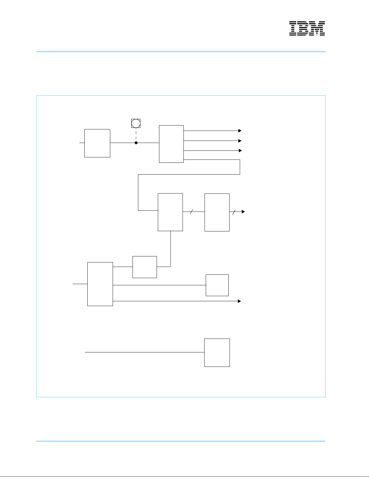
2. Board Design
Figure 2-1 illustrates the architecture of the PPC750FX evaluation board. Subsequent sections discuss
aspects of Figure 2-1 in more detail.
Figure 2-1. PPC750FX Board Architecture
PCI
Connector
ATX
Power
Connector
100/10
Fast
Ethernet
x2
System
PCI
Memory
Bus
Controller
and PCI
Bridge
Board Power
DDR
SDRAM
60x Bus
CPU 0
JTAG/RISCWatch
CPU 1
Interrupts
Boot
SEEPROM
CPLD
SEEPROM
Flash/SRAM
NVRAM
Serial Port
x2
4-Pin
2.1 Processor
The PPC750FX evaluation board is based upon the PPC750FX processor. See Section 1.1 PowerPC 750FX
RISC Microprocessor Features on page 13 for details. There are two PPC750FX processors on this board.
750FXebm_ch2.fm
June 10, 2003
Board Design
Page 19 of 115
Page 20
Evaluation Board Manual
PPC750FX Evaluation Board Preliminary
2.2 Board Clocking
The clock architecture of the PPC750FX board is illustrated in Figure 2-2.
Figure 2-2. Clock Distribution on the PPC750FX Board
External clock
(see Note)
MK74CB218
Clock
Driver
133MHz @ 2.5V
133MHz @ 2.5V
133MHz @ 3.3V
133MHz @ 3.3V
CPU 0
CPU 1
CPLD
33.33MHz Osc
C9531AT
Clock
Generator
133MHz
25MHz Osc
3.6864MHz Osc
Clock
Buffer
25MHz
25MHz
25MHz
Clock
Multiplier
MV64360
System
Controller
125MHz
2
ICS93V857
Clock
Driver
BCM5222
Dual
Ethernet
PHY
STI6C2552
Dual
UART
10
DDR SDRAM
CPLD
Board Design
Page 20 of 115
Note : Rework to the board is required to use the external oscillator input.
750FXebm_ch2.fm
June 10, 2003
Page 21

Evaluation Board Manual
Preliminary PPC750FX Evaluation Board
2.3 Internal Processor Clocking
The PPC750FX requires a single system clock input SYSCLK. The frequency of this input determines the
frequency of the PPC750FX bus interface. Internally, the PPC750FX uses a phase-lock loop (PLL) circuit to
generate a master core clock that is frequency-multiplied and phase-locked to the SYSCLK input. The PLL in
the PPC750FX is configured using seven pins PLL_CFG(0:4) and PLL_RANGE(0:1). On the PPC750FX
evaluation board, the configuration of these pins is controlled by switch settings (see Section 6 Switches on
page 39).
2.4 System Controller
The board contains a Marvell MV64360 system controller that connects to the 60x bus of the PPC750FX, and
provides an interface to DDR SDRAM, the PCI bus, the integrated Ethernet MACs, the integrated SRAM, an
interrupt controller, DMA engines, and an interface to attach external devices. Hereafter, in this document,
this component is referred to as the system controller.
2.5 SDRAM Interface
This board provides 256MB of permanently mounted DDR SDRAM operating at 133.33MHz. The interface to
the SDRAM is through the system controller, and is accessed using DRAM chip selects CS0 and CS1. The
SDRAM on the board is 72 bits wide and allows the use of the SDRAM Error Checking and Correction (ECC)
feature in the system controller if desired.
2.6 PCI Bus
This PPC750FX evaluation board is a full-length PCI card and is intended to be operated while plugged into a
PCI slot in a personal computer or a PCI backplane. However, because an ATX power connector is provided,
it can be operated without being plugged into a PCI slot. If this external mode of operation is used, the PCI
bus will not be available.
2.7 Ethernet
The board provides two 100BASE-TX Ethernet interfaces. The physical layer for both Ethernet ports is
provided by the BCM5222 which contains two medium-independent interface (MII) PHYs. The five address
pins of the BCM5222 are tied to ground making the addresses of the two PHYs 0 and 1. Tab le 2- 1 shows the
relationship between the two Ethernet ports being used in the MV64360, the PHY to which each port is
connected in the BCM5222, the address of each PHY, and finally the RJ45 connectors for each port (see J20
in Figure 10-1 on page 54).
Table 2-1. Ethernet Ports
MV64360 Ethernet Port No. BCM522 PHY No.
0211
1102
750FXebm_ch2.fm
June 10, 2003
Serial Manangement Interface
PHY Address
RJ45 Connector
Board Design
Page 21 of 115
Page 22

Evaluation Board Manual
PPC750FX Evaluation Board Preliminary
Figure 2-3. Board Ethernet Architecture
MV64360
System
Controller
Ethernet
Ports
0
1
MDIO/MDC
MII
MII
Dual PHY
2
1
2
BCM5222
SMI 1
SMI 0
J8064D628A
2
1
1
2
RJ45 Sockets
w/ Magnetics and LEDs
The supported media is Category 5A Unshielded Twisted Pair cable (UTP), accessed via two RJ45
connectors on the board. The two RJ45 connectors are in a common housing with integrated magnetics and
LEDS.
2.8 Flash Memory
The following describes how to access Flash memory directly on the board.
Eight-bit Flash memory is used on the PPC750FX board. No benchmarking impact is expected from the use
of a narrow rather than a wide Flash array. For performance work, one should expect to replace the initial
firmware support provided in the Flash with more optimized routines residing in DRAM.
The PPC750FX board contains 1MB of 8-bit wide Flash memory provided by two socketed 8b x 0.5Mb
modules, and 32MB of 32-bit wide Flash memory provided by two 16b x 16Mb module (+3.3V only) for data
or code storage. Additionally, 1MB of SRAM, provided as two 512 KB modules, can be used in this memory
space.
The board can be set to boot from 8-bit wide Flash with SRAM below it in memory or, alternatively, it can boot
from the SRAM with the 8-bit wide Flash below it in memory. This setup uses system controller chip select
BootCS.
When set up to use BootCS to boot from 8-bit wide Flash or from SRAM, the system controller chip select
CS0 is used to select the 32-bit wide Flash. If desired, these chip selects can be swapped so that the board
will boot from the 32-bit wide Flash using BootCS, then CS0 selects the 8-bit wide Flash/SRAM combination.
There are two switches used to control where the system controller chip selects are directed. See System
Controller Initialization on page 42 for details on U17 switch 6 and U24 switch 7.
Board Design
Page 22 of 115
750FXebm_ch2.fm
June 10, 2003
Page 23

Evaluation Board Manual
Preliminary PPC750FX Evaluation Board
The 8-bit wide Flash is installed at the top of the address space. Immediately below that Flash in the address
space is the SRAM. Switch #7 on switch U24 allows the exchange of the two blocks in the address space.
The intent of this SRAM is to aid in the debug of ROM boot code, not for speed enhancement. Flash contents
will be copied to SRAM, then SRAM will be placed at the top of the address space. ROM code can then be
debugged from SRAM, allowing the placement of unlimited software break points.
Note 1: A jumper at J8 can be installed to prevent any 32-bit Flash write operations.
Note 2: Caching the 8- or 32-bit Flash memories is not supported.
Tab le 2-2 and Tab le 2- 3 describe the switch settings and the resulting configurations.
Table 2-2. Switch Settings
Configuration U17 SW6 U24 SW 7 Description
1 ON ON 8-bit boot, Flash at higher address
2 ON OFF 8-bit boot, SRAM at higher address
3 OFF ON 32-bit boot, Flash at higher address
4 OFF OFF 32-bit boot, SRAM at higher address
Table 2-3. Flash Configurations
Configuration Address Range Module(s) selected
0xFFF00000 to 0xFFFFFFFF 8-bit Flash controlled by BootCS
1
2
3
4
Notes: 1. The reset vector of the PPC750FX is 0xFFF00100.
2. The base addresses of peripherals attached to the MV64360 system controller device are software dependent. The values
0xFFE00000 to 0xFFEFFFFF 8-bit SRAM controlled by BootCS
0xFC000000 to 0xFDFFFFFF 32-bit Flash controlled by DevCS0
0xFFF00000 to 0xFFFFFFFF 8-bit SRAM controlled by BootCS
0xFFE00000 to 0xFFEFFFFF 8-bit Flash controlled by BootCS
0xFC000000 to 0xFDFFFFFF 32-bit Flash controlled by DevCS0
0xFE000000 to 0xFFFFFFFF 32-bit Flash controlled by BootCS
0xFC100000 to 0xFC1FFFFF 8-bit Flash controlled by DevCS0
8-bit SRAM controlled by DevCS0.
0xFC000000 to 0xFC0FFFFF
0xFE000000 to 0xFFFFFFFF 32-bit Flash controlled by BootCS
0xFC100000 to 0xFC1FFFFF 8-bit SRAM controlled by DevCS0
0xFC000000 to 0xFC0FFFFF
in the table above are used by the PPC750FX Evaluation Kit Software. Other software environments may use different
values for the peripheral base addresses.
Note: In configuration 3, SRAM is at the beginning of the DevCS0 memory
range followed by 8-bit wide Flash.
8-bit Flash controlled by DevCS0.
Note: In configuration 4, 8-bit wide Flash is at the beginning of the DevCS0
memory range followed by SRAM.
750FXebm_ch2.fm
June 10, 2003
Board Design
Page 23 of 115
Page 24

Evaluation Board Manual
PPC750FX Evaluation Board Preliminary
2.9 NVRAM
The board provides 32KB of non-volatile RAM. This memory is attached to the system controller device
interface, and is accessed using chip select DevCS3. This particular type of non-volatile ram uses magnetic
core technology and is referred to in the board schematics as FRAM. It does not require any battery power to
maintain its contents.
2.10 SRAM
The PPC750FX evaluation board provides 1MB of permanently mounted SRAM. This memory interfaces to
the system controller. Access to this memory by the processors is through the system controller. Address
space for SRAM is shared with Flash memory. See Flash Memory on page 22 for details on how the address
space can be configured.
In addition to the SRAM on the board, there are 256KB of addressible SRAM integrated in the system
controller module.
2.11 Serial Ports
The board utilizes an Exar ST16C2552 DUART to provide two 16550 compatible UARTs. The DUART is
attached to the device interface of the system controller, and is accessed using chip select DevCS2. Each
UART provides four interface signals (Tx, Rx, DSR, DTR) and is connected to an RJ11/12 connector.
Both serial ports are clocked by the same 3.68MHz oscillator provided on the board.
The Multi-Protocol Serial Controllers in the system controller are not supported on the PPC750FX evaluation
board.
Figure 2-4. Board Serial Port Architecture
ST16C2552
Dual UART
1 (A)
2 (B)
RJ11/12 Sockets
1 (Right)
2 (Left)
Board Design
Page 24 of 115
750FXebm_ch2.fm
June 10, 2003
Page 25

Evaluation Board Manual
Preliminary PPC750FX Evaluation Board
2.12 Logic Analyzer Connections
The system controller device bus is attached to Mictor logic analyzer connectors.
HP Logic analyzer connection to the PCI bus is accomplished using a FuturePlus PCI Local Bus Passive
Analysis Probe, vendor part number FS2005. The customer may purchase this probe from the manufacturer.
Probe hardware does not ship with the board.
2.13 Power Supply
The PPC750FX evaluation board obtains its power from the PCI slot connector into which it is plugged or
from the on-board ATX power connector.
2.13.1 PCI Voltages
The voltages provided through the PCI slot connector are:
•+5V
•+3.3V
All of the voltages described in the following sections are developed from the +3.3V PCI voltage.
2.13.2 System Controller Voltages
The system controller requires four voltages:
• System controller I/O—+3.3V
• DRAM —+2.5V
• CPU I/O—+2.5V
• System controller logic and Ethernet—+1.8V
Note: There are no external connection points for the +1.8V or +2.5V supplies. As a result variable
voltage testing and current measurement capability for these supplies are not available.
2.13.3 PPC750FX Voltages
The PPC750FX chip requires two voltages:
• Logic and PLL analog circuits— +1.45V
• 60x bus I/O circuits— +2.5V
Both voltages are generated by on-board regulators from the +3.3V voltage. Current measurement points are
available for both voltages. These measurement points can also be used to connect external voltage
supplies.
Note: The 60x bus voltage supply to the PPC750FX can be +1.8V, +2.5V, or +3.3V. To use any voltage
other than the +2.5V supplied by the board, the voltage must be supplied externally, and the 60x voltage
selection signals to the PPC750FX must be programmed accordingly.
750FXebm_ch2.fm
June 10, 2003
Board Design
Page 25 of 115
Page 26

Evaluation Board Manual
PPC750FX Evaluation Board Preliminary
2.13.4 SDRAM Voltages
An on-board regulator supplies +2.5V to the DDR SDRAM. This voltage is also the supply for the DRAM
interface in the system controller.There is also a +1.25V reference voltage provided to the SDRAM. There is
no current measurement point provided for this voltage.
2.14 Form Factor
The PPC750FX board is a full-length PCI card intended to be plugged into and operated in a standard PCI
slot on a personal computer or a PCI backplane. If a personal computer or PCI backplane are not available, it
can operate stand-alone with an external ATX power supply connected at J34.
Board Design
Page 26 of 115
750FXebm_ch2.fm
June 10, 2003
Page 27

Evaluation Board Manual
Preliminary PPC750FX Evaluation Board
3. Memory Map
Table 3-1 provides a summary of the board address space usage. For details about address space usage
relating to the processor registers, refer to the PPC750FX Embedded Processor User’s Manual.
Table 3-1. Board Address Space Usage
Peripheral Start Address End Address Chip Select Size
DDR SDRAM 0x00000000 0x0FFFFFFF SDRAM CS0 and CS1 256MB
MV64360 Integrated SRAM 0x42000000 0x4203FFFF n/a 256KB
FRAM 0xEF500000 0xEF507FFF DevCS3 32KB
ST16C2552 UART Channel B 0xEF600000 0xEF600007 DevCS2 8B
ST16C2552 UART Channel A 0xEF600008 0xEF60000F DevCS2 8B
CPLD Registers 0xEF700000 0xEF700004 DevCS1 5B
MV64360 Registers 0xF1000000 0xF100FFFF n/a 64KB
32-bit Flash 0xFC000000 0xFDFFFFFF DevCS0 32MB
SRAM 0xFFE00000 0xFFEFFFFF BootCS 1MB
8-bit Flash 0xFFF00000 0xFFFFFFFF BootCS 1MB
Note: The base addresses of peripherals attached to the MV64360 system controller device are software dependent. The values in the
table above are used by the PPC750FX Evaluation Kit Software. Other software environments may use different values for the
peripheral base addresses.
3.1 CPLD Register Definitions
This section provides description by bit for each of the CPLD registers.
Each CPLD register is 8 bits wide. In the tables below, the most significant bit is bit 0, and the least significant
bit is bit 7. The CPLD source code uses the reverse bit ordering.
Table 3-2. Register0
Bit Name R/W Description
0:7 CPLD Revision R Revision level of CPLD code
750FXebm_ch3.fm
June 10, 2003
Memory Map
Page 27 of 115
Page 28

Evaluation Board Manual
PPC750FX Evaluation Board Preliminary
Table 3-3. Register1
Note: This register should be written before reading in order to latch the most current status. Any value can be written to the register.
Bit Name R/W Description
0 (msb) na na Unused
1 na na Unused
2 ATX or PCI Power R
3 Spare Switch B R
4 Spare Switch A R
5 PCI Adapter/Host select R
6 8-bit Flash/SRAM swap select R
7 (lsb) BootFlash select R
0 = Using an ATX power supply
1 = Power obtained from a PCI slot
0 = U35 Switch 8 is ON
1 = U35 Switch 8 is OFF
0 = U30 Switch 8 is ON
1 = U30 Switch 8 is OFF
0 = PCI Host mode U24 Switch 6 is ON
1 = PCI Adapter mode U24 Switch 6 is OFF
0 = 8-bit Flash is at a higher address in memory, U24 Switch 6 is ON
1 = 8-bit SRAM is at a higher address in memory, U24 Switch 6 is ON
0 = Booted from 8-bit flash or SRAM U17 Switch 6 is ON
1 = Booted from 32-bit flash U17 Switch 6 is OFF
Table 3-4. Register2
Bit Name R/W Description
0 (msb) CPU1 MCP control R/W
1 CPU0 MCP control R/W
2 CPU TBEN control R/W
3 CPU1 SMI control R/W
4 CPU0 SMI control R/W
5 DS4 LED control R/W
6 DS2 LED control R/W
7 (lsb) DS1 LED control R/W
Asserts the Machine Check Pin (MCP) signal on CPU1
0 = CPU1 MCP signal not asserted
1 = CPU1 MCP signal asserted
Asserts the Machine Check Pin (MCP) signal on CPU0
0 = CPU0 MCP signal not asserted
1 = CPU0 MCP signal asserted
Controls the state of the timebase enable (TBEN) signal of both CPUs
0 = timebase runs freely on both CPUs
1 = timebase frozen on both CPUs
Asserts the System Management Interrupt signal on CPU1
0 = CPU1 SMI signal not asserted
1 = CPU1 SMI signal asserted
Asserts the System Management Interrupt signal on CPU0
0 = CPU0 SMI signal not asserted
1 = CPU0 SMI signal asserted
0 = DS4 LED is ON
1 = DS4 LED is OFF
0 = DS2 LED is ON
1 = DS2 LED is OFF
0 = DS1 LED is ON
1 = DS1 LED is OFF
Memory Map
Page 28 of 115
750FXebm_ch3.fm
June 10, 2003
Page 29

Evaluation Board Manual
Preliminary PPC750FX Evaluation Board
Table 3-5. Register3
Bit Name R/W Description
Five MPP/GPP pins on the system controller can be used to control
the SRESET and HRESET of pins of the processors, and an entire
board reset. To give software a chance to configure the MPP/GPP
0 (msb) Block MPP resets R/W
1:7 unused
pins 7, 8, 11, 12, and 24 properly, the signals are blocked by the
CPLD until this bit is set to 1.
0 = MPP resets are blocked
1 = MPP resets are not blocked
Table 3-6. Register4
Bit Name R/W Description
0:7 Board Revision R
Board revision level in binary (for example, 0x00000010 = Revision
level 2).
750FXebm_ch3.fm
June 10, 2003
Memory Map
Page 29 of 115
Page 30

Evaluation Board Manual
PPC750FX Evaluation Board Preliminary
Memory Map
Page 30 of 115
750FXebm_ch3.fm
June 10, 2003
Page 31

Evaluation Board Manual
Preliminary PPC750FX Evaluation Board
4. Programming the System Controller
This section provides guidance on programming the system controller to agree with the board design.
4.1 DDR SDRAM
The following are the characteristics of the DDR SDRAM memory on the PPC750FX evaluation board:
Table 4-1. DDR SDRAM Characteristics
Memory Type DDR SDRAM
Number of Row Addresses 13
Number of Column Addresses 9
Number of Module Banks 2
SDRAM Width, Primary 16 bits
Error Checking SDRAM Width 8 bits
Data Width 72 bits
Number of SDRAM Banks 4
4.1.1 SDRAM Controller Initialization
See Marvell MV64360/1/2 data sheet.
4.2 Device Controller Bank Register Settings
The following sections define the settings for the device controller bank registers in the system controller.
750FXebm_ch4.fm
June 10, 2003
Programming the System Controller
Page 31 of 115
Page 32

Evaluation Board Manual
PPC750FX Evaluation Board Preliminary
4.2.1 Device Bank 0 Parameters (32-bit Flash)
Table 4-2. Device Bank 0 Parameters = 0x85A492BF
Field Value (bin) Comment
TurnOff 111
Acc2First 0111
Acc2Next 0101
ALE2Wr 010 Number of Sysclk cycles from ALE de-assertion to the assertion of Wr[0]
WrLow 010 Number of Sysclk cycles that Wr[0] is active
WrHigh 010
DevWidth 10 Device width of 32 bits
TurnOffExt 0 TurnOff extension (most significant bit)
Acc2FirstExt 1 Acc2First extension (most significant bit)
Acc2NextExt 1 Acc2Next extension (most significant bit)
ALE2WrExt 0 ALE2Wr extension (most significant bit)
WrLowExt 1 WrLow extension (most significant bit)
WrHighExt 0 WrHigh extension (most significant bit)
BadrSkew 00 Number of Sysclk cycles from when BAdr changes to the read of the data
DPEn 0 Parity Disabled
Reserved 1
Number of Sysclk cycles that the system controller does not drive the
address/data bus after completion of a device read
Number of Sysclk cycles from the de-assertion of ALE to the cycle that the
first read data is sampled
Number of Sysclk cycles in a burst read access between the cycle that
samples data N to the cycle that samples data N+1
Number of Sysclk cycles between data beats of a burst write that Wr[0] is
held in-active. BAdr and data are held valid for WrHigh-1 cycles
Programming the System Controller
Page 32 of 115
750FXebm_ch4.fm
June 10, 2003
Page 33

Evaluation Board Manual
Preliminary PPC750FX Evaluation Board
4.2.2 Device Bank 1 Parameters (CPLD registers)
Table 4-3. Device Bank 1 Parameters = 0x8004921A
Field Value (bin) Comment
TurnOff 010
Acc2First 0011
Acc2Next 0100
ALE2Wr 010 Number of Sysclk cycles from ALE de-assertion to the assertion of Wr[0]
WrLow 010 Number of Sysclk cycles that Wr[0] is active
WrHigh 010
DevWidth 00 Device width of 8 bits
TurnOffExt 0 TurnOff extension (most significant bit)
Acc2FirstExt 0 Acc2First extension (most significant bit)
Acc2NextExt 0 Acc2Next extension (most significant bit)
ALE2WrExt 0 ALE2Wr extension (most significant bit)
WrLowExt 0 WrLow extension (most significant bit)
WrHighExt 0 WrHigh extension (most significant bit)
BadrSkew 00 Number of Sysclk cycles from when BAdr changes to the read of the data
DPEn 0 Parity Disabled
Reserved 1
Number of Sysclk cycles that the system controller does not drive the
address/data bus after completion of a device read
Number of Sysclk cycles from the de-assertion of ALE to the cycle that the
first read data is sampled
Number of Sysclk cycles in a burst read access between the cycle that
samples data N to the cycle that samples data N+1
Number of Sysclk cycles between data beats of a burst write that Wr[0] is
held in-active. BAdr and data are held valid for WrHigh-1 cycles
750FXebm_ch4.fm
June 10, 2003
Programming the System Controller
Page 33 of 115
Page 34

Evaluation Board Manual
PPC750FX Evaluation Board Preliminary
4.2.3 Device Bank 2 Parameters (UARTs)
Table 4-4. Device Bank 2 Parameters = 0x8C002BD6
Field Value (bin) Comment
TurnOff 110
Acc2First 1010
Acc2Next 0111
ALE2Wr 101 Number of Sysclk cycles from ALE de-assertion to the assertion of Wr[0]
WrLow 000 Number of Sysclk cycles that Wr[0] is active
WrHigh 000
DevWidth 00 Device width of 8 bits
TurnOffExt 0 TurnOff extension (most significant bit)
Acc2FirstExt 0 Acc2First extension (most significant bit)
Acc2NextExt 0 Acc2Next extension (most significant bit)
ALE2WrExt 0 ALE2Wr extension (most significant bit)
WrLowExt 1 WrLow extension (most significant bit)
WrHighExt 1 WrHigh extension (most significant bit)
BadrSkew 00 Number of Sysclk cycles from when BAdr changes to the read of the data
DPEn 0 Parity Disabled
Reserved 1
Number of Sysclk cycles that the system controller does not drive the
address/data bus after completion of a device read
Number of Sysclk cycles from the de-assertion of ALE to the cycle that the
first read data is sampled
Number of Sysclk cycles in a burst read access between the cycle that
samples data N to the cycle that samples data N+1
Number of Sysclk cycles between data beats of a burst write that Wr[0] is
held in-active. BAdr and data are held valid for WrHigh-1 cycles
Programming the System Controller
Page 34 of 115
750FXebm_ch4.fm
June 10, 2003
Page 35

Evaluation Board Manual
Preliminary PPC750FX Evaluation Board
4.2.4 Device Bank 3 Parameters (FRAM)
Table 4-5. Device Bank 3 Parameters = 0x8D891445
Field Value (bin) Comment
TurnOff 101
Acc2First 1000
Acc2Next 010
ALE2Wr 010 Number of Sysclk cycles from ALE de-assertion to the assertion of Wr[0]
WrLow 100 Number of Sysclk cycles that Wr[0] is active
WrHigh 100
DevWidth 00 Device width of 8 bits
TurnOffExt 0 TurnOff extension (most significant bit)
Acc2FirstExt 1 Acc2First extension (most significant bit)
Acc2NextExt 1 Acc2Next extension (most significant bit)
ALE2WrExt 0 ALE2Wr extension (most significant bit)
WrLowExt 1 WrLow extension (most significant bit)
WrHighExt 1 WrHigh extension (most significant bit)
BadrSkew 00 Number of Sysclk cycles from when BAdr changes to the read of the data
DPEn 0 Parity Disabled
Reserved 1
Number of Sysclk cycles that the system controller does not drive the
address/data bus after completion of a device read
Number of Sysclk cycles from the de-assertion of ALE to the cycle that the
first read data is sampled
Number of Sysclk cycles in a burst read access between the cycle that
samples data N to the cycle that samples data N+1
Number of Sysclk cycles between data beats of a burst write that Wr[0] is
held in-active. BAdr and data are held valid for WrHigh-1 cycles
750FXebm_ch4.fm
June 10, 2003
Programming the System Controller
Page 35 of 115
Page 36

Evaluation Board Manual
PPC750FX Evaluation Board Preliminary
4.2.5 Boot Device Parameters (8 bit flash and SRAM)
If booting from the 8-bit Flash or SRAM, the default value of the Boot Device Parameters register in the
system controller is 0x8FCFFFFF. To improve the access time to the Flash contents, the register can be
changed to the following:
Table 4-6. Boot Device Bank Parameters = 0x8185D09E
Field Value (bin) Comment
TurnOff 110
Acc2First 0011
Acc2Next 010
ALE2Wr 010 Number of Sysclk cycles from ALE de-assertion to the assertion of Wr[0]
WrLow 111 Number of Sysclk cycles that Wr[0] is active
WrHigh 010
DevWidth 00 Device width of 8 bits
TurnOffExt 0 TurnOff extension (most significant bit)
Acc2FirstExt 1 Acc2First extension (most significant bit)
Acc2NextExt 1 Acc2Next extension (most significant bit)
ALE2WrExt 0 ALE2Wr extension (most significant bit)
WrLowExt 0 WrLow extension (most significant bit)
WrHighExt 0 WrHigh extension (most significant bit)
BadrSkew 00 Number of Sysclk cycles from when BAdr changes to the read of the data
DPEn 0 Parity Disabled
Reserved 1
Number of Sysclk cycles that the system controller does not drive the
address/data bus after completion of a device read
Number of Sysclk cycles from the de-assertion of ALE to the cycle that the
first read data is sampled
Number of Sysclk cycles in a burst read access between the cycle that
samples data N to the cycle that samples data N+1
Number of Sysclk cycles between data beats of a burst write that Wr[0] is
held in-active. BAdr and data are held valid for WrHigh-1 cycles
Programming the System Controller
Page 36 of 115
750FXebm_ch4.fm
June 10, 2003
Page 37

Evaluation Board Manual
Preliminary PPC750FX Evaluation Board
5. Reset and Interrupts
The following sections provide details regarding the reset and interrupt operation of the board.
5.1 Resets
Reset to the PPC750FX is generated at power-on, by the reset pushbutton, by system-reset from the
PPC750FX (usually in response to a command from the RISCWatch debugger), or by undervoltage on the
+3.3V supply.
Under software control, using registers in the CPLD, each processor can be reset individually, or the entire
board can be reset.
5.2 Interrupts
The system controller contains an interrupt controller that handles interrupts from peripherals inside the
system controller as well as external peripherals.
There are three external interrupt inputs to the PPC750FX (INT, MCP, and SMI). See Table 5-1 for more
detail.
Figure 5-1. Interrupt Architecture
MV64360
CPU 0
INT
MCP
SMI
CPU 1
SMI
MCP
INT
UART A
UART B
Ethernet PHY
PCI Intr A
PCI Intr B
PCI Intr C
PCI Intr D
System Controller
CPLD
Register2
750FXebm_ch5.fm
June 10, 2003
Reset and Interrupts
Page 37 of 115
Page 38

Evaluation Board Manual
PPC750FX Evaluation Board Preliminary
Table 5-1. External Interrupts
MPP Controller Pin +/- Active Sensitivity Description
25 + level UART Channel A
26 + level UART Channel B
27 – level Ethernet PHY
28 – level PCI Intr A
29 – level PCI Intr B
30 – level PCI Intr C
31 – level PCI Intr D
Note: The PCI interrupts are inputs when the board is operating as a PCI host. If operating as a PCI adapter, these pins should be
configured as outputs.
Reset and Interrupts
Page 38 of 115
750FXebm_ch5.fm
June 10, 2003
Page 39

Evaluation Board Manual
Preliminary PPC750FX Evaluation Board
6. Switches
This section shows the location of all the switches on the board, and explains the function of each switch.
Table 6-1. Switches
Location Function Page
U5 Reset pushbutton 39
U17, U24 System controller initialization 42
U30 CPU 0 PLL configuration 40
U35 CPU 1 PLL configuration 41
U53 External ATX power 40
Figure 6-1. Switch Location Diagram
U5
On
U53
ATX Power
Off
Off
Off
1
8
1
8
1
8
1
8
Reset
U17
On
U24
U30
On
U35
6.1 Reset Pushbutton
When pressed, the pushbutton switch at U5 pulls the PWRGD signal to ground, causing a reset of the board.
Table 6-2. Reset Pushbutton—U5
Signal Description (0 = ON = close)
Pulls down PWRGD. Main board reset.
750FXebm_ch6.fm
June 10, 2003
Switches
Page 39 of 115
Page 40

Evaluation Board Manual
PPC750FX Evaluation Board Preliminary
6.2 ATX Power-on Pushbutton
When pressed, the pushbutton switch at U53 generates a power-on signal to the external ATX power supply
connected to J34. This pushbutton must be pressed after the ATX power supply is connected to J34 in order
to activate the power supply
Note: If the board is plugged into a PCI slot, the external ATX power supply will not activate under any
conditions, and pressing U53 will have no effect.
Table 6-3. Reset Pushbutton—U53
Signal Description (0 = ON = close)
PS_ON Generates power-on signal to the external ATX power connector.
6.3 CPU 0 PLL Configuration
An 8-position DIP switch at location U30 configures the PLL for the first PPC750FX processor (U1).
Table 6-4. CPU 0 PLL Configuration—U30
Switch No. Signal Default Setting Description (0 = ON = closed, 1 = OFF = open)
1 PLL_CONFIG0 ON
2 PLL_CONFIG1 OFF
3 PLL_CONFIG2 ON
4 PLL_CONFIG3 OFF
5 PLL_CONFIG4 OFF
6 PLL_RANGE0 ON
7 PLL_RANGE1 ON
8 SPARESWITCH1 ON
Refer to the latest version of the PowerPC 750FX
RISC Microprocessor Data Sheet for details on the bit
settings for PLL_CONFIG and PLL_RANGE.
Input to CPLD F2 pin with pull-up to +3.3V. See CPLD
Register1.
Switches
Page 40 of 115
750FXebm_ch6.fm
June 10, 2003
Page 41

Evaluation Board Manual
Preliminary PPC750FX Evaluation Board
6.4 CPU 1 PLL Configuration
An 8-position DIP switch at location U35 configures PLL for the second PPC750FX processor (U2).
Table 6-5. CPU 1 PLL Configuration Switches—U35
Switch No. Signal Default Setting Description (0 = ON = closed, 1= OFF = open)
1 PLL_CONFIG0 ON
2 PLL_CONFIG1 OFF
3 PLL_CONFIG2 ON
4 PLL_CONFIG3 OFF
5 PLL_CONFIG4 OFF
6 PLL_RANGE0 ON
7 PLL_RANGE1 ON
8 SPARESWITCH2 ON Connected to +3.3V pull-up. See CPLD Register1.
Refer to the latest version of the PowerPC 750FX
RISC Microprocessor Data Sheet for details on the bit
settings for PLL_CONFIG and PLL_RANGE.
750FXebm_ch6.fm
June 10, 2003
Switches
Page 41 of 115
Page 42

Evaluation Board Manual
PPC750FX Evaluation Board Preliminary
6.5 System Controller Initialization
Two 8-position DIP switches at location U17 and U24 provide initilization settings for the system controller.
Table 6-6. System Controller Initilization—U17
Switch No. Signal Default Setting Description (0 = ON = closed, 1 = OFF = open)
1DEV_AD0 ON
2:3 DEV_AD2:DEV_AD3 ON:ON
4DEV_AD5 OFF
5DEV_AD8 OFF
6DEV_AD15 ON
7DEV_AD16 OFF
8DEV_AD18 OFF
ON = MV64360 Serial ROM initialization disabled
OFF = MV64360 Serial ROM initialization enabled
Specifies the two least significant bits of the 7 bit IIC address of the Serial
ROM the MV64360 can use for initialization.
ON:ON = address 0b1010000 (Serial EEPROM U36)
ON:OFF = reserved
OFF:ON = address 0b1010001 (Serial EEPROM U55)
OFF:OFF = reserved
ON = MV64360 register base address is 0x14000000
OFF = MV64360 register base address is 0xF1000000
ON = MV64360 CPU Pads Calibration Disabled
OFF = MV64360 CPU Pads Calibration Enabled
ON = boot from 8 bit socketed Flash BOOTSMALL_N
OFF = boot from 32 bit Flash
ON = MV64360 PCI retry disabled
OFF = MV64360 PCI retry enabled
ON = DDR-SDRAM clock is running at a higher frequency than the
MV64360 core clock
OFF = DDR-SDRAM clock is running at the same frequency as the
MV64360 core clock
Switches
Page 42 of 115
750FXebm_ch6.fm
June 10, 2003
Page 43

Evaluation Board Manual
Preliminary PPC750FX Evaluation Board
Table 6-7. System Controller Initilization—U24
Switch No. Signal Default Setting Description (0 = ON = closed, 1 = OFF = open)
ON = DDR SDRAM address/control signals toggle on falling edge of
1DEV_AD19 OFF
2DEV_AD21 ON
3DEV_AD22 ON
4DEV_AD23 ON
5DEV_AD24 ON
6
7 FLASH_N/SRAM_SEL ON
8DEV_AD14 ON
PCIMODE_TARGET/
HOST_N
OFF
DRAM clock.
OFF = DDR SDRAM address/control signals toggle on rising edge of
DRAM clock.
ON = DDR SDRAM two pipe stages (up to 133MHz SDRAM clock)
OFF = DDR SDRAM three pipe stages (up to 183MHz SDRAM clock)
ON = DDR SDRAM read data is synchronized to the MV64360 core clock.
OFF = DDR SDRAM read data is synchronized to the MV64360 FBClkIn
clock signal.
DDR SDRAM Read Control Logic Delay
ON = Disabled
OFF = Enabled
DDR SDRAM Read Data Delay
ON = Disabled
OFF = Enabled
ON = board operates as a PCI Host
OFF = board operates as a PCI Adapter
ON = 8-bit Flash resides at a higher address than the 8-bit SRAM
OFF = 8-bit SRAM resides at a higher address than the 8-bit Flash
Note: This switch can be useful for putting SRAM at the CPU reset vector
during boot ROM code development.
This switch should always be in the ON position since only 8- or 32-bit
wide devices are available for booting.
750FXebm_ch6.fm
June 10, 2003
Switches
Page 43 of 115
Page 44

Evaluation Board Manual
PPC750FX Evaluation Board Preliminary
Switches
Page 44 of 115
750FXebm_ch6.fm
June 10, 2003
Page 45

Evaluation Board Manual
Preliminary PPC750FX Evaluation Board
7. Fuses, Batteries, Regulators, and Fans
This evaluation board is a PCI card and contains no fuses, batteries, or user-adjustable regulators. All supply
voltages needed for the various board components are developed by fixed, board-mounted regulators that
use the voltage provided through the PCI edge connector or the ATX power connector. There are three onboard voltages that can be monitored for current drain or replaced with external voltage sources for variable
voltage testing.
There is one fan installed on the board that cools the two processor chips.
7.1 On-Board Current Monitoring and Variable Voltage Testing
The PPC750FX logic, PLL, and 60X bus voltages can be monitored for current drain. In addition, external
supplies can be connected in place of the fixed, on-board regulators to perform variable voltage testing.
Removal of zero-ohm resistors, as shown in Figure 7-1, is required to implement current measurement or
supply substitution.
Figure 7-1. Resistor Location Diagram
R224
12
R226
R267
12
R271
R307
12
R312
7.1.1 1.45V Supplies
The PPC750FX uses +1.45 V for the logic and PLL voltages. There are two +1.45V supplies on the board.
They are identified as VCCA1 and VCCA2. A pair of zero-ohm resistors can be removed for either of both
supplies to create a connection point or points for current measurement or external supply connection.
Figure 7-1 shows the location of the zero-ohm resistors. Current measurements can be made between
terminals 1 and 2 of either resistor. External supplies should be connected to terminal 2.
Table 7-1. Current Measurement of the1.4V Supplies
Voltage Remove resistors at:
VCCA1 R267 and R271
750FXebm_ch7.fm
June 10, 2003
Fuses, Batteries, Regulators, and Fans
Page 45 of 115
Page 46

Evaluation Board Manual
PPC750FX Evaluation Board Preliminary
Table 7-1. Current Measurement of the1.4V Supplies
Voltage Remove resistors at:
VCCA2 R307 and R312
7.1.2 2.5V Supply
The PPC750FX uses 2.5V for the 60x bus. There is one 2.5V supply on the board. It is identified as VCCA3.
A pair of zero-ohm resistors can be removed to create a connection point or points for current measurement
or external supply connection. Figure 7-1 shows the location of the zero-ohm resistors. Current
measurements can be made between terminals 1 and 2 of either resistor. External supplies should be
connected to terminal 2.
Table 7-2. Current Measurement of the 2.5V Supply
Voltage Remove resistors at:
VCCA3 R224 and R226
7.2 Fan
There is one fan provided on the board. This fan is mounted on the processor heatsinks and cools both of the
processor chips. See Figure 7-2. The system controller chip has a heatsink attached, but no fan.
Figure 7-2. Fan and Heatsink Location Diagram
DS3
Processor Heatsinks
System Controller Heatsink
J16
Fan
The processor fan is connected to J4. If the Ignore Fan jumper at J16 is not installed, programming in the
CPLD activates LED DS3 when a failure is detected at connector J4, and shuts down the power to the
processors and the sytem controller. Disconnecting the fan is detected as a failure.
J4
Power Cable
Ignore
Fan
Fuses, Batteries, Regulators, and Fans
Page 46 of 115
750FXebm_ch7.fm
June 10, 2003
Page 47
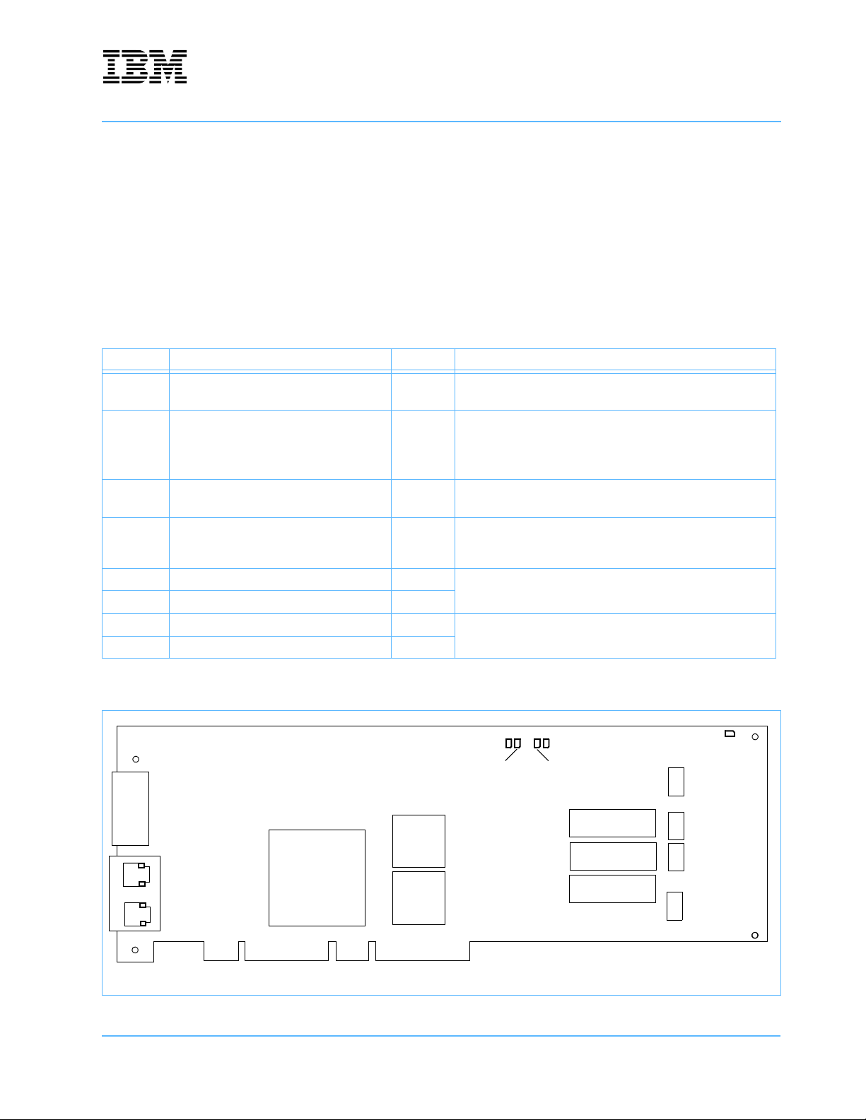
Evaluation Board Manual
Preliminary PPC750FX Evaluation Board
8. Displays
There are nine LED displays on the board. Table 8-1 identifies the location, color and function of each
display. Figure 8-1 shows the location on the board.
Note: There are four Ethernet status LEDs integrated in the two-port Ethernet connector at J20. There are
two LEDs per port which are physically located at the corners of each of the two sockets. Each of the two
sockets is assigned to one of the Ethernet ports 1 or 2. The location designation L (left) and R (right) applies
when the connector is oriented horizontally and viewed looking into the sockets.
Table 8-1. Displays
Location Name Color Description
DS1
DS2
DS3 RED_LED Red
DS4 LED2 Amber
DS5 ATX_OK_LED_N Green
J20 2 L Ethernet Link, Port 1 Green
J20 2 R Ethernet Activity, Port 1 Yellow
J20 1 L Ethernet Link, Port 2 Green
J20 1 R Ethernet Activity, Port 2 Yellow
LED0
LED1
Green
CPLD status
User programmable by setting bits in a CPLD register.
Board problem.
1. SYSRESET_N signal is active
2. Fan failure (Not running or disconnected)
3. Jumper J16 installed.
CPLD status
User programmable by setting bits in a CPLD register.
ATX power
Indicates power from external ATX supply connected at J34 is
good.
Dual LEDs, part of the RJ45 Ethernet 1 port, indicating
Ethernet status.
Dual LEDs, part of the RJ45 Ethernet 2 port, indicating
Ethernet status.
Figure 8-1. Display Location Diagram
L
1
R
L
R
750FXebm_ch8.fm
June 10, 2003
J20
2
DS1
DS2
DS4
DS3
DS5
Displays
Page 47 of 115
Page 48

Evaluation Board Manual
PPC750FX Evaluation Board Preliminary
Displays
Page 48 of 115
750FXebm_ch8.fm
June 10, 2003
Page 49

Evaluation Board Manual
Preliminary PPC750FX Evaluation Board
9. Jumpers
The location, type, and function for all jumpers on the board are described in the following sections.
Table 9-1. Jumpers
Location Function Page
J8 32-bit Flash write protection 50
J16 Ignore Fan 50
J22 PCI interrupt selection 51
J27–J30 Factory test only (not populated) –
Figure 9-1. Jumper Location Diagram
DS3
J8
1
4
J16
J22
8
5
750FXebm_ch9.fm
June 10, 2003
Jumpers
Page 49 of 115
Page 50

Evaluation Board Manual
PPC750FX Evaluation Board Preliminary
9.1 Write-Protect 32-Bit Flash
32-bit Flash memory can be rendered read-only (write-protected) by this jumper. This is a 1x2 Berg type
header.
Figure 9-2. Write-Protect 32-bit Flash Memory Jumper—J8
12
Table 9-2. Write-Protect 32-bit Flash Memory—J8
J8 Description Factory Setting
1–2 Write Protected (read-only)
Open Write Enabled X
9.2 Ignore Fan
There is one fan on this board that cools both of the PPC750FX processor modules. The connector for the
fan power provides a feedback signal to the CPLD indicating a properly functioning fan. When the jumper at
J16 is installed, the fan is not monitored. Removing the jumper at J16 allows LED DS3 to be activated if the
fan fails or is not connected.
In normal operation, a fan failure causes the power to the processors and system controller to be shut down.
The J16 jumper can be used to avoid this power shutdown if the user wishes to continue operation following
a fan failure. It is the user’s responsibility to ensure that adequate cooling is available to the processors and
system controller if the fan is not operating and J16 is installed.
Note: If the jumper at J16 is installed, the Check Fan LED is turned on as an indication to the user that the
fan is not being monitored.
These are 1x2 Berg type headers.
Figure 9-3. Ignore Fan Jumper—J16
12
Table 9-3. Ignore Fans—J16
J16 Description Factory Setting
1–2 Ignore fan
Open Monitor fan X
Jumpers
Page 50 of 115
750FXebm_ch9.fm
June 10, 2003
Page 51

Evaluation Board Manual
Preliminary PPC750FX Evaluation Board
9.3 PCI Interrupt Selection
Jumper J22 configures the adapter mode PCI interrupt output from the system controller to one or more of the
four PCI interface interrupts. This a 2x4 Berg type header.
Figure 9-4. PCI Interrupt Selection Jumper—J22
87 65
12 34
Table 9-4. PCI Interrupt Selection—J22
J22 Description Factory Setting
1–8 Adapter mode interrupt to PCI interrupt A X
2–7 Adapter mode interrupt to PCI interrupt B
3–6 Adapter mode interrupt to PCI interrupt C
4–5 Adapter mode interrupt to PCI interrupt D
750FXebm_ch9.fm
June 10, 2003
Jumpers
Page 51 of 115
Page 52

Evaluation Board Manual
PPC750FX Evaluation Board Preliminary
Jumpers
Page 52 of 115
750FXebm_ch9.fm
June 10, 2003
Page 53

Evaluation Board Manual
Preliminary PPC750FX Evaluation Board
10. Connectors
The location, type, function, and pin assignment for all board connections are described in the following
sections. Connectors are listed in Table 10-1 and shown in Figure 10-1. Test connections are described in
Section 10.12 and shown in Figure 10-13.
Table 10-1. Connectors
Location Function Page
J34 ATX Power 55
J4 CPU Fan Power 56
J11 RISCWatch JTAG 57
J13 RJ11, Serial Ports 1 (Right) and 2 (Left) 63
J14 System Controller Device Address Bus 64
J15 Memory Control 66
J19 Spare Connector –
J20 RJ45, Ethernet Ports 1(Left) and 2 (Right) 58
J25 PCI Connector 59
J26 CPLD JTAG Connector 62
Jxx Ground connectors: J1, J2, J7, J9, J10, J12, J17, J18, J23, J24 56
J31–J33,
J36–J45
U39 SMA, External Clock Input 68
TPxx Test Connections 69
Factory test only (not populated) –
750FXebm_ch10.fm
June 10, 2003
Connectors
Page 53 of 115
Page 54

Evaluation Board Manual
PPC750FX Evaluation Board Preliminary
Figure 10-1. Connector Location Diagram, Top Side
J1
GND
GND
8
7
L
2
1
1
2
J10
2
1
J13
8
7
R
2
1
1
2
GND
L
7
J17
8
J20
1
2
R
7
8
J18
GND GND
GND
J2
J11
J4
2
115
GND
J12
16
J14
J15
2
J26
1
J19
U39
J23
2 1
20
10
2
1
2
1
2
1
GND
GND
J9
38
37
38
37
38
37
J24
B14
B12
B1
J25
B49
B52
B62
B63
B94
Keying slots
GND
J7
11
J34
1
Note: PCI contacts A1 through A94 mirror the B1-B94 contacts on the bottom side of the card.
Connectors
Page 54 of 115
750FXebm_ch10.fm
June 10, 2003
Page 55

Evaluation Board Manual
Preliminary PPC750FX Evaluation Board
10.1 Auxiliary Power
The board is equipped with a standard ATX power connector. This allows the board to be externally powered
from a standard ATX power supply when it is not installed in a PCI slot.
Note: If the board is plugged into a PCI slot, the external ATX power supply will not activate under any
conditions, and pressing the ATX power-on pushbutton (U53) will have no effect.
Figure 10-2. ATX Power Supply Connector—J34
12345678910
11 12 13 14 15 16 17 18 19 20
Table 10-2. ATX Power Signals—J34
Pin Name Comment
1 +3.3V Tolerance ± 4%
2 +3.3V Tolerance ± 4%
3GND
4 +5V Tolerance ± 5%
5GND
6 +5V Tolerance ± 5%
7GND
8 Power OK Active high indicator that +5V and +3.3V are above their undervoltage thresholds
9 +5V SB Standby power, at least 10 mA, tolerance ± 5%
10 +12V Not used
11 +3.3V Tolerance ± 4%. Remote 3.3V sense.
12 -12V Not used
13 GND
14 PS-ON Active low signal that turns on the ATX power supply.
15 GND
16 GND
17 GND
18 -5V Not used
19 +5V Tolerance ± 5%
20 +5V Tolerance ± 5%
750FXebm_ch10.fm
June 10, 2003
Connectors
Page 55 of 115
Page 56

Evaluation Board Manual
PPC750FX Evaluation Board Preliminary
10.2 Ground
Test points for grounding logic analyzers and other test equipment are available on these connectors. These
are 1x1 Berg type connectors.
Figure 10-3. Ground Connectors—J1, J2, J7, J9, J10, J12, J17, J18, J23, J24
1
Table 10-3. Ground Connectors —J1, J2, J7, J9, J10, J12, J17, J18, J23, J24
Pin Signal Name
1GND
10.3 Fan Power
There is one connector available at J4 for powering the fan that cools the two processor chips.
Figure 10-4. Fan Power Connector—J4
3
2
1
Table 10-4. Fan Power Signals—J4,
Pin Signal Name
1GND
2+5V
3
Fan feedback
Note: A low (near 0V) feedback signal from the fan is an indication that the fan is running.
Connectors
Page 56 of 115
750FXebm_ch10.fm
June 10, 2003
Page 57

Evaluation Board Manual
Preliminary PPC750FX Evaluation Board
10.4 RISCWatch JTAG Debugger
The RISCWatch JTAG debugger connects to the board through a 2x8 header.
Figure 10-5. RISCWatch JTAG Connector—J11
216
115
Table 10-5. RISCWatch Signals—J11
Pin Signal Name
1TDO
2 unused
3TDI
4TRST_N
5 unused
6PWRSENSE
7TCK
8 unused
9TMS
10 unused
11 SRESET_N
12 unused
13 HRESET_N
14 Key—no pin at this location.
15 CHECKSTOP_N
16 GND
750FXebm_ch10.fm
June 10, 2003
Connectors
Page 57 of 115
Page 58

Evaluation Board Manual
PPC750FX Evaluation Board Preliminary
10.5 Ethernet
This board provides two Ethernet ports. The connections are through a single housing at J20 that contains
two RJ45 connectors. Each connector contains integral magnetics and two LEDs. The ports are identified as
1 and 2. Both ports can be configured for Fast (10/100 Mbps) Ethernet interfaces, and can be used with
Category 5 Unshielded Twisted-Pair (UTP) cable.
Figure 10-6. Ethernet Connector—One of two RJ45 Sockets in J20
12345678
LEDs
Table 10-6. Ethernet UTP Signals—J20, both sockets
Pin Signal Name Description
1 RD+ Receive data +
2RD
3 TD+ Transmit data +
4 RCT Receive center tap
5 TCT Transmit center tap
6TD
7 NC No connection
8 GND Ground
− Receive data −
− Transmit data −
Connectors
Page 58 of 115
750FXebm_ch10.fm
June 10, 2003
Page 59

Evaluation Board Manual
Preliminary PPC750FX Evaluation Board
10.6 PCI Connector
This evaluation board is a PCI card. It has a standard PCI connector that plugs into a standard +3.3V or +5V
PCI socket on a PC system board. The signals on the PCI conector are the standard set of PCI signals.
Figure 10-7. PCI Connector—J25
Key slots
A1 A62A11 A14
B1 B62B11 B14
Note: This view of the connector is from the top edge of the card.
Table 10-7. PCI Connector Signals—J25
Pin Signal Pin Signal
B1 -12V A1 TRST
B2 TCK A2 +12V
B3 GND A3 TMS
B4 TDO A4 TDI
B5 +5V A5 +5V
B6 +5V A6 INTA
B7 INTB A7 INTC
B8 INTD A8 +5V
B9 PRSNT1 A9 Reserved
B10 Reserved A10 +3.3V (I/O)
B11 PRSNT2 A11 Reserved
–
––
B14 Reserved A14 +3.3V (Aux)
B15 GND A15 RST
B16 CLK A16 +3.3V (I/O)
B17 GND A17 GNT
B18 REQ A18 GND
B19 +3.3V (I/O) A19 Reserved
B20 AD31 A20 AD30
B21 AD29 A21 +3.3V
Key slot
A49
B49
A52
B52
A63 A94
B63 B94
–
Key slot
750FXebm_ch10.fm
June 10, 2003
Connectors
Page 59 of 115
Page 60

Evaluation Board Manual
PPC750FX Evaluation Board Preliminary
Table 10-7. PCI Connector Signals—J25 (Continued)
Pin Signal Pin Signal
B22 GND A22 AD28
B23 AD27 A23 AD26
B24 AD25 A24 GND
B25 +3.3V A25 AD24
B26 C/BE3 A26 IDSEL
B27 AD23 A27 +3.3V
B28 GND A28 AD22
B29 AD21 A29 AD20
B30 AD19 A30 GND
B31 +3.3V A31 AD18
B32 AD17 A32 AD16
B33 C/BE2 A33 +3.3V
B34 GND A34 FRAME
B35 IRDY A35 GND
B36 +3.3V A36 TRDY
B37 DEVSEL A37 GND
B38 GND A38 STOP
B39 LOCK A39 +3.3V
B40 PERR A40 Reserved
B41 +3.3V A41 Reserved
B42 SERR A42 GND
B43 +3.3V A43 PAR
B44 C/BE1 A44 AD15
B45 AD14 A45 +3.3V
B46 GND A46 AD13
B47 AD12 A47 AD11
B48 AD10 A48 GND
B49 M66EN/GND A49 AD9
–
––
B52 AD8 A52 C/BE0
B53 AD7 A53 +3.3V
B54 +3.3V A54 AD6
B55 AD5 A55 AD4
B56 AD3 A56 GND
B57 GND A57 AD2
B58 AD1 A58 AD0
Key slot
–
Key slot
Connectors
Page 60 of 115
750FXebm_ch10.fm
June 10, 2003
Page 61

Evaluation Board Manual
Preliminary PPC750FX Evaluation Board
Table 10-7. PCI Connector Signals—J25 (Continued)
Pin Signal Pin Signal
B59 +3.3V (I/O) A59 +3.3V (I/O)
B60 ACK64 A60 REQ64
B61 +5V A61 +5V
B62 +5V A62 +5V
–
––
B63 Reserved A63 GND
B64 GND A64 C/BE7
B65 C/BE6 A65 C/BE5
B66 C/BE4 A66 +3.3V(I/O)
B67 GND A67 PAR64
B68 AD63 A68 AD62
B69 AD61 A69 GND
B70 +3.3V(I/O) A70 AD[60]
B71 AD[59] A71 AD58
B72 AD57 A72 GND
B73 GND A73 AD56
B74 AD55 A74 AD54
B75 AD53 A75 +3.3V(I/O)
B76 GND A76 AD52
B77 AD51 A77 AD50
B78 AD49 A78 GND
B79 +3.3V(I/O) A79 AD48
B80 AD47 A80 AD46
B81 AD45 A81 GND
B82 GND A82 AD44
B83 AD43 A83 AD42
B84 AD41 A84 +3.3V(I/O)
B85 GND A85 AD40
B86 AD39 A86 AD38
B87 AD37 A87 GND
B88 +3.3V(I/O) A88 AD36
B89 AD35 A89 AD34
B90 AD33 A90 GND
B91 GND A91 AD32
Key slot
–
Key slot
750FXebm_ch10.fm
June 10, 2003
Connectors
Page 61 of 115
Page 62

Evaluation Board Manual
PPC750FX Evaluation Board Preliminary
Table 10-7. PCI Connector Signals—J25 (Continued)
Pin Signal Pin Signal
B92 Reserved A92 Reserved
B93 Reserved A93 GND
B94 GND A94 Reserved
10.7 CPLD JTAG Connector
The CPLD may be programmed in place on the board via this JTAG connector and appropriate
downloading software. This is a 2x5 Berg type connector.
Figure 10-8. CPLD JTAG Connector—J26
246 108
Table 10-8. CPLD JTAG Connector—J26
Pin Signal Name
1ISP_TCK
2GND
3ISP_TDO
4 +3.3V
5ISP_TMS
6 unused
7 unused
8 unused
9ISP_TDI
10 GND
135 97
Connectors
Page 62 of 115
750FXebm_ch10.fm
June 10, 2003
Page 63

Evaluation Board Manual
Preliminary PPC750FX Evaluation Board
10.8 Serial Ports
Serial Port 1 (J13 Right) and Serial Port 2 (J13 Left) are provided through standard RJ11/12 connectors, as
shown in Figure 10-9. Both serial port interfaces are provided by the ST16C2552 attached to the system
controller and support only four RS-232 signals.
Table 10-9 describes the pin assignments for Serial Ports 1 and 2. Note that DTR appears on both pins 2
and 7.
Figure 10-9. Serial Port Connector—J13, one of two RJ11/12 sockets
1234567
Table 10-9. Serial Port Connector Signals—J13, both ports
Pin Signal Name
1 Empty contact position
2DTR
3DSR
4Rx
5 Frame Ground
6Tx
7DTR
8 Empty contact positiont
8
750FXebm_ch10.fm
June 10, 2003
Connectors
Page 63 of 115
Page 64

Evaluation Board Manual
PPC750FX Evaluation Board Preliminary
10.9 System Controller Device Address Bus
Connection to HP logic analyzers via HP E5346A High Density Probe Adapters is provided by board mounted
connectors, Mictor Part Number 2-767004-2. This connector provides user access to the system controller
peripheral address bus for test and debug purposes.
Figure 10-10. System Controller Device Address Connector—J14
37
38
Table 10-10. System Controller Device Address Signals—J14
Pin Analyzer Signal Name
1 unused
2 unused
3 GND
4 unused
5 addr_pod0 – CLK ALE
6 addr_pod1 – CLK unused
7 addr_pod0 – D15 DEV_ADR(31)
8 addr_pod1 – D15 DEV_ADR(15)
9 addr_pod0 – D14 DEV_ADR(30)
10 addr_pod1 – D14 DEV_ADR(14)
11 addr_pod0 – D13 DEV_ADR(29)
12 addr_pod1 – D13 DEV_ADR(13)
13 addr_pod0 – D12 DEV_ADR(28)
14 addr_pod1 – D12 DEV_ADR(12)
15 addr_pod0 – D11 DEV_ADR(27)
16 addr_pod1 – D11 DEV_ADR(11)
17 addr_pod0 – D10 DEV_ADR(26)
18 addr_pod1 – D10 DEV_ADR(10)
19 addr_pod0 – D9 DEV_ADR(25)
20 addr_pod1 – D9 DEV_ADR(9)
21 addr_pod0 – D8 DEV_ADR(24)
22 addr_pod1 – D8 DEV_ADR(8)
23 addr_pod0 – D7 DEV_ADR(23)
1
2
Connectors
Page 64 of 115
750FXebm_ch10.fm
June 10, 2003
Page 65

Evaluation Board Manual
Preliminary PPC750FX Evaluation Board
Table 10-10. System Controller Device Address Signals—J14 (Continued)
Pin Analyzer Signal Name
24 addr_pod1 – D7 DEV_ADR(7)
25 addr_pod0 – D6 DEV_ADR(22)
26 addr_pod1 – D6 DEV_ADR(6)
27 addr_pod0 – D5 DEV_ADR(21)
28 addr_pod1 – D5 DEV_ADR(5)
29 addr_pod0 – D4 DEV_ADR(20)
30 addr_pod1 – D4 DEV_ADR(4)
31 addr_pod0 – D3 DEV_ADR(19)
32 addr_pod1 – D3 DEV_ADR(3)
33 addr_pod0 – D2 DEV_ADR(18)
34 addr_pod1 – D2 DEV_ADR(2)
35 addr_pod0 – D1 DEV_ADR(17)
36 addr_pod1 – D1 DEV_ADR(1)
37 addr_pod0 – D0 DEV_ADR(16)
38 addr_pod1 – D0 DEV_ADR(0)
750FXebm_ch10.fm
June 10, 2003
Connectors
Page 65 of 115
Page 66

Evaluation Board Manual
PPC750FX Evaluation Board Preliminary
10.10 Memory Control
Connection to HP logic analyzers via HP E5346A High Density Probe Adapters is provided by board mounted
connectors, Mictor Part Number 2-767004-2. This connector carries the burst address bus and the chip select
signals from the system controller.
Figure 10-11. Memory Control Connector—J15
37
38
1
2
Table 10-11. Memory Control Signals—J15
Pin Analyzer Signal Name
1 unused
2 unused
3 GND
4 unused
5 cntl_pod0 – CLK unused
6 cntl_pod1 – CLK unused
7 cntl_pod0 – D15 BADR(2)
8 cntl_pod1 – D15 TESTPIN_A
9 cntl_pod0 – D14 BADR(1)
10 cntl_pod1 – D14 SRAM_LO_CS_N
11 cntl_pod0 – D13 BADR(0)
12 cntl_pod1 – D13 unused
13 cntl_pod0 – D12 SMALL_FLASH_LO_CS
14 cntl_pod1 – D12 unused
15 cntl_pod0 – D11 DEV_WE(3)
16 cntl_pod1 – D11 unused
17 cntl_pod0 – D10 DEV_WE(2)
18 cntl_pod1 – D10 SYSRESET_N
19 cntl_pod0 – D9 DEV_WE(1)
20 cntl_pod1 – D9 CPU1_HRESET_2.5_N
21 cntl_pod0 – D8 DEV_WE(0)
22 cntl_pod1 – D8 CPU1_SRESET_2.5_N
23 cntl_pod0 – D7 CS_TIMING_N
Connectors
Page 66 of 115
750FXebm_ch10.fm
June 10, 2003
Page 67

Evaluation Board Manual
Preliminary PPC750FX Evaluation Board
Table 10-11. Memory Control Signals—J15 (Continued)
Pin Analyzer Signal Name
24 cntl_pod1 – D7 CPU0_HRESET_2.5_N
25 cntl_pod0 – D6 NVRAM_CS_N
26 cntl_pod1 – D6 CPU0_SRESET_2.5_N
27 cntl_pod0 – D5 BIG_FLASH_CS_N
28 cntl_pod1 – D5 unused
29 cntl_pod0 – D4 SMALL_FLASH_HI_CS_N
30 cntl_pod1 – D4 TESTPIN_D
31 cntl_pod0 – D3 SRAM_HI_CS_N
32 cntl_pod1 – D3 TESTPIN_B
33 cntl_pod0 – D2 READ_N
34 cntl_pod1 – D2 unused
35 cntl_pod0 – D1 WRITE_N
36 cntl_pod1 – D1 FPGA_CS_N
37 cntl_pod0 – D0 UART_CS_N
38 cntl_pod1 – D0 TESTPIN_C
750FXebm_ch10.fm
June 10, 2003
Connectors
Page 67 of 115
Page 68

Evaluation Board Manual
PPC750FX Evaluation Board Preliminary
10.11 External Clock Input
An external 133MHz board clock may be provided by an external oscillator connected to this board-mounted
SMA connector. The oscillator output should have 3.3V logic levels. The input impedance to this connector is
approximately 50
Note: Board rework is required to use this connector. See the schematic diagrams.
Figure 10-12. External Clock Input Connector—U39
Ω.
34
5
12
Table 10-12. External Clock Input Signal—U39
Pin Signal Name
1 Ground
2 Ground
3 Ground
4 Ground
5 CLK_EXT
Connectors
Page 68 of 115
750FXebm_ch10.fm
June 10, 2003
Page 69

Evaluation Board Manual
Preliminary PPC750FX Evaluation Board
10.12 Test Connections
Access to selected points in the board circuits, not available through connectors or jumpers, is provided by
small test connections. All of the test connections are small pads with a center hole. An electrical connection
can be made to any of these test connections for test purposes. These test connections are documented in
the schematic, in Table 10-13, and in Figure 10-13.
There are two kinds of test connections. The basic difference between the two is the size of the pad and the
center hole. One type of test connection is called a test point and has a large pad and center hole. Test points
are suitable for soldering wires to them for test and design purposes. The reference designators for test
points are TPnn where nn are numbers. The other type of test connection is called an ehole or test access
via. These test connections have a very small pad and center hole. The reference designators for eholes are
Unn where nn are numbers.
To determine what signal the test connection connects to, refer to the schematic. In Figure 10-13, the test
connections are labeled with their reference designators only. The actual pad and hole is not shown. Other
major components on the board are shown for assistance in locating the test connections.
Table 10-13. Test Connections
Location Component Signal
TP1 U20 LBOOT_CS_N
TP2 U20 LDEV_RW_N
TP3 U18 +2.5V VADJ
TP4 U50 P07
TP5 U50 INT_N
TP6 U3 System Controller CS2_N
TP7 U3 System Controller CS3_N
TP8 U3 System Controller JTD0
TP9 U1 750FX QREQ0
TP10 U50 P17
TP11 U3 System Controller MPP13
TP12 U1 750FX WTI
TP13 U3 System Controller MPP16
TP14 U3 System Controller MPP15
TP15 U1 750FX CI
TP16 U3 System Controller DEVDP0
TP17 U1 750FX RSRV0
TP18 U3 System Controller MPP18
TP19 U3 System Controller MPP17
TP20 U3 System Controller DEVDP1
TP21 U1 750FX CLK_OUT0
TP22 U3 System Controller DEVDP3
750FXebm_ch10.fm
June 10, 2003
Connectors
Page 69 of 115
Page 70

Evaluation Board Manual
PPC750FX Evaluation Board Preliminary
Table 10-13. Test Connections (Continued)
Location Component Signal
TP23 U3 System Controller MPP3
TP24 U3 System Controller MPP2
TP25 U3 System Controller MPP1
TP27 U3 System Controller MPP6
TP28 U3 System Controller MPP4
TP29 U3 System Controller MPP5
TP30 U3 System Controller MPP14
TP31 U3 System Controller MPP27
TP32 U3 System Controller MPP20
TP33 U2 750FX QREQ1
TP34 U3 System Controller MPP22
TP35 U3 System Controller ENUM_N
TP36 U2 750FX WT
TP37 U2 750FX RSRV1
TP38 U2 750FX CLK_OUT1
TP39 U2 750FX T4
TP41 U3 System Controller MPP0
TP42 U3 System Controller MPP9
TP43 U3 System Controller MPP10
U26 U27 VREF_IN
U28 U27 SHDN_N
Connectors
Page 70 of 115
750FXebm_ch10.fm
June 10, 2003
Page 71

Evaluation Board Manual
Preliminary PPC750FX Evaluation Board
Figure 10-13. Test Connection Locations
TP1
TP2
TP3
U26
U28
TP8
TP16
TP20
TP22
TP23
TP25
TP28
TP30
TP24
TP27
TP29
TP6 TP7
TP41*
TP42*
TP43*
TP32
TP35
TP31
TP34
TP9
TP12
TP15
TP17
TP21
TP36
TP37
TP38
TP39
TP33
TP11
TP13
TP14
TP19
TP18
* TP41, TP42, and TP43 are located on the bottom of the board
TP5
TP4
TP10
750FXebm_ch10.fm
June 10, 2003
Connectors
Page 71 of 115
Page 72

Evaluation Board Manual
PPC750FX Evaluation Board Preliminary
Connectors
Page 72 of 115
750FXebm_ch10.fm
June 10, 2003
Page 73
Evaluation Board Manual
Preliminary PPC750FX Evaluation Board
11. CPLD Programming
This chapter contains logic of the CPLD (formerly FPGA) module and timing values for the signals associated
with the CPLD.
Table 11-1. Section Contents
Description Page
Programming—Registers and Control Functions 73
Timing—Registers and Control Functions 94
11.1 Programming—Registers and Control Functions
General software functions such as address decoding and board status registers are provided by the CPLD
at U29. The following figures provide a combined graphical and textual representation of the functional
programming within the CPLD.
11.1.1 I/O Pin List
Table 11-2 lists all of the signals entering and exiting the CPLD module. The module pin number and I/O
function are shown.
Note: Pins that are labeled as
∼NAME∼ are special purpose pins defined by the CPLD to program functions
or set reference voltages.
Table 11-2. CPLD I/O Pin List
Name Pin Function
cpu0_chkstop_n 1 Input
ale 2 Input
VCCIO1 3 Power
~TDI~ 4 Input
rw_trst 5 Input
sram_hi_cs_n 6 Output
small_flash_hi_cs_n 7 Output
badr[1] 8 Input
led0 9 Output
led2 10 Output
GND 11 Gnd
~VREFA~ 12 Input
fpga_cs_n 13 Output
pci_reset_n 14 Bidir
750FXebm_ch11.fm
June 10, 2003
CPLD Programming
Page 73 of 115
Page 74

Evaluation Board Manual
PPC750FX Evaluation Board Preliminary
Table 11-2. CPLD I/O Pin List (Continued)
Name Pin Function
~TMS~ 15 Input
write_n 16 Output
uart_cs_n 17 Output
VCCIO1 18 Power
nvram_cs_n 19 Output
led1 20 Output
led_red_n 21 Output
ignore_fans_n 22 Input
mpp0_sreset_n 23 Input
cpu1_chkstop_n 24 Input
sysreset 25 Output
GND 26 Gnd
dev_adr[5] 27 Bidir
dev_adr[6] 28 Bidir
dev_adr[7] 29 Bidir
sysreset_n 30 Output
mpp1_hreset_n 31 Input
NOFAN_N 32 Output
sram_cs_n 33 Output
VCCIO1 34 Power
small_flash_cs_n 35 Output
read_n 36 Output
big_flash_cs_n 37 Output
GND 38 Gnd
VCCINT 39 Power
badr[0] 40 Input
initact 41 Input
flash_n/sram_sel 42 Input
GND 43 Gnd
lcs_n[2] 44 Input
pwrgd 45 Input
switch_a 46 Input
testpin_c 47 Output
testpin_b 48 Output
testpin_a 49 Output
textpin_d 50 Output
VCCIO2 51 Power
CPLD Programming
Page 74 of 115
750FXebm_ch11.fm
June 10, 2003
Page 75

Evaluation Board Manual
Preliminary PPC750FX Evaluation Board
Table 11-2. CPLD I/O Pin List (Continued)
Name Pin Function
cpu0_hreset_n 52 Output
cpu_trst_n 53 Output
cpu1_sreset_n 54 Output
cpu1_hreset_n 55 Output
cpu0_sreset_n 56 Output
lcs_n[1] 57 Input
mpp_reset_out_n 58 Input
GND 59 Gnd
~VREFB~ 60 Input
atx_ok_n 61 Input
~TCK~ 62 Input
dev_we_n[0] 63 Input
lcs_n[0] 64 Input
bootsmall_n 65 Input
VCCIO2 66 Power
badr[2] 67 Input
rw_sreset 68 Input
jtag_chkstop_n 69 Output
cpu_tben 70 Output
cpu1_smi_n 71 Output
cpu0_smi_n 72 Output
~TDO~ 73 Output
GND 74 Gnd
lcs_n[3] 75 Input
mpp0_hreset_n 76 Input
ldev_addr[21] 77 Input
cstiming_n 78 Input
unused_pin 79 Output
cpu_mcp1 80 Output
cpu_mcp0 81 Output
VCCIO2 82 Power
mpp1_sreset_n 83 Input
rw_hreset 84 Input
switch_b 85 Input
GND 86 Gnd
pld_sysclk 87 Input
target/host_n 88 Input
750FXebm_ch11.fm
June 10, 2003
CPLD Programming
Page 75 of 115
Page 76

Evaluation Board Manual
PPC750FX Evaluation Board Preliminary
Table 11-2. CPLD I/O Pin List (Continued)
Name Pin Function
GND+ 89
pld25mhz 90 Input
VCCINT 91 Power
dev_adr[0] 92 Bidir
dev_adr[1] 93 Bidir
dev_adr[2] 94 Bidir
GND 95 Gnd
dev_adr[3] 96 Bidir
dev_adr[4] 97 Bidir
ldev_addr[20] 98 Input
cpufan_ok_n 99 Input
ldev_addr[19] 100 Input
11.1.2 CPLD Logic
The folllowing sections provided a representation of the logic of the complete CPLD in either graphical or
code listing format.
Table 11-3. CPLD Logic Descriptions
Section Description Page
Top Level Block Diagram 1 First three of five CPLD logic sections 77
Top Level Block Diagram 2 Last two of five CPLD logic sections 78
framcs Logic framcs detailed logic diagram 79
decode_block Program decode_block code listing 80
registers2 Program register2 code listing 84
reset_block Program reset_block code listing 89
misc Logic misc detailed logic diagram 93
CPLD Programming
Page 76 of 115
750FXebm_ch11.fm
June 10, 2003
Page 77

Evaluation Board Manual
Preliminary PPC750FX Evaluation Board
11.1.2.1 Top Level Block Diagram 1
framcs
badr0
badr1
badr2
pld_sysclk
sysreset_n
lcs_n3
cstiming_n
sysreset_n
PLD_SYSCLK
cstiming_n
lboot_cs_n
lcs_n[3..0]
ldev_addr[21..19]
flash_n/sram_sel
bootsmall_n
ldevr_w_n
dev_we_n[0]
nvram_burst_cs_n
badr0
badr1
badr2
sysclock
sysreset
lcs_n[3]
cstiming_n
inst4
decode_block
sysreset_n
sysclk
CSTiming_n
LBootCS_n
lcs_n[3..0]
ldev_addr[21..19]
flash_n/sram_sel
bootsmall_n
ldevR_W_n
Dev_We_n0
nvram_burst_cs_n
inst7
nvram_burst_cs_n
small_flash_lo_cs_n
small_flash_hi_cs_n
sram_lo_cs_n
sram_hi_cs_n
big_flash_cs_n
Read_n
Write_n
uart_cs_n
nvram_cs_n
test
fpga_cs_n
nvram_burst_cs_n
small_flash_cs_n
small_flash_hi_cs_n
sram_cs_n
sram_hi_cs_n
big_flash_cs_n
read_n
write_n
uart_cs_n
nvram_cs_n
testpin_d
fpga_cs_n
sysreset_n
cstiming_n
dev_we_n[0]
ale
fpga_cs_n
badr[2..0]
target/host_n
flash_n/sram_sel
bootsmall_n
switch_a
switch_b
atx_ok_n
750FXebm_ch11.fm
June 10, 2003
registers2
sysreset_n
cstiming_n
we_n0
ale
fpga_cs_n
badr[2..0]
target/host_n
flash_n/sram_sel
bootsmall_n
switch_a
switch_b
ATX_OK_N
inst
dev_ad[7..0]
ldevR_W_n
lboot_cs_n
led0
led1
led2
cpu0_smi_n
cpu1_smi_n
cpu_tben
cpu_mcp0
cpu_mcp1
read_oe
mpp_block_n
dev_adr[7..0]
ldevr_w_n
lboot_cs_n
led0
led1
led2
cpu0_smi_n
cpu1_smi_n
cpu_tben
cpu_mcp0
cpu_mcp1
mpp_block_n
CPLD Programming
Page 77 of 115
Page 78

Evaluation Board Manual
j
j
PPC750FX Evaluation Board Preliminary
11.1.2.2 Top Level Block Diagram 2
reset_block
pld25mhz
rw_hreset
rw_sreset
rw_trst
mpp_reset_2ms_n
mpp0_hreset_n
mpp0_sreset_n
mpp1_hreset_n
mpp1_sreset_n
mpp_reset_out_n
initact
powergood
target/host_n
serial_eeprom
cpufan_ok_n
ignore_fans_n
mpp_block_n
atx_ok_n
25Mclk
rw_hreset
rw_sreset
rw_trst
mpp_reset_2ms_n
mpp0_hreset_n
mpp0_sreset_n
mpp1_hreset_n
mpp1_sreset_n
mpp_reset_out_n
initact
pgd
target/host_n
serial_eeprom
cpufan_ok_n
ignore_fans_n
mpp_block_n
ATX_OK_N
pci_reset_n
sysreset_n
cpu0_hreset_n
cpu0_sreset_n
cpu1_hreset_n
cpu1_sreset_n
cpu_trst_n
nofan_n
sloclk
led_red_n
sysreset
pci_reset_n
sysreset_n
cpu0_hreset_n
cpu0_sreset_n
cpu1_hreset_n
cpu1_sreset_n
cpu_trst_n
NOFAN_N
sloclk
led_red_n
sysreset
pld25mhz
mpp_reset_out_n
mpp_block_n
pwrgd
dev_adr0
sysreset_n
cpu0_chkstop_n
cpu1_chkstop_n
inst5
misc
pld25mhz
mpp_reset_out_n
mpp_block_n
pwrgd
dev_adr0
sysreset_n
cpu0_chkstop_n
cpu1_chkstop_n
inst3
mpp_reset_2ms_n
del_powergood
serial_eeprom
tag_chkstop_n
mpp_reset_2ms_n
powergood
serial_eeprom
tag_chkstop_n
CPLD Programming
Page 78 of 115
750FXebm_ch11.fm
June 10, 2003
Page 79

Evaluation Board Manual
q
q
q
Preliminary PPC750FX Evaluation Board
11.1.2.3 framcs Logic
The following logic diagram defines the function of the logic in the framcs part of the CPLD:
Date: May 6, 2003 framcs.bdf Project: top
lpm_dff0
lpm_dff0
lpm_dff0
aclr
aclr
aclr
DFF
DFF
DFF
qadr0
qadr1
qadr2
badr2
badr0
badr1
INPUT
GND
INPUT
GND
INPUT
GND
inst2
inst
inst1
data
clock
enable
data
clock
enable
data
clock
enable
sysclock
sysreset
lcs_n[3]
cstiming_n
NOT
inst13
INPUT
VCC
INPUT
VCC
INPUT
VCC
INPUT
VCC
badr0
qadr0
badr1
qadr1
badr2
qadr2
NOT
inst14
lpm_xor0
inst7
lpm_xor0
inst8
lpm_xor0
inst9
lpm_or0
inst10
OUTPUT
nvram_burst_cs_n
750FXebm_ch11.fm
June 10, 2003
CPLD Programming
Page 79 of 115
Page 80

Evaluation Board Manual
PPC750FX Evaluation Board Preliminary
11.1.2.4 decode_block Program
The following code listing defines the function of the logic in the decode_block part of the CPLD:
INCLUDE "lpm_ff.inc"; -- 10:30 AM Mar 26, 2003
INCLUDE "lpm_counter.inc";
SUBDESIGN decode_block
(
sysreset_n : INPUT;
sysclk : INPUT;
CSTiming_n : INPUT;
LBootCS_n : INPUT; -- 16 Bit flash/sram or 32 bit FLASH (32MB) chip select
lcs_n[3..0] : INPUT; -- latched from upper address/data bus
ldev_addr[21..19] : INPUT; -- latched device address. Note that this is not the PowerPC conventional
-- address ordering. Device Addr0 is the LSB.
flash_n/sram_sel : INPUT;
bootsmall_n : INPUT;
ldevR_W_n : INPUT;
Dev_We_n0 : INPUT;
nvram_burst_cs_n: INPUT;
)
VARIABLE
small_flash_lo_cs_n: OUTPUT; -- default lboot_cs_n, swappable to lcs_n[0]
small_flash_hi_cs_n: OUTPUT; -- default lboot_cs_n, swappable to lcs_n[0]
sram_lo_cs_n : OUTPUT; -- default lboot_cs_n, swappable to lcs_n[0]
sram_hi_cs_n : OUTPUT; -- default lboot_cs_n, swappable to lcs_n[0]
big_flash_cs_n : OUTPUT; -- default lcs_n[0], swappable to lboot_cs_n
Read_n : OUTPUT;
Write_n : OUTPUT;
uart_cs_n : OUTPUT; -- lcs_n[2]
nvram_cs_n : OUTPUT; -- lcs_n[3]
test : OUTPUT; -- test only
fpga_cs_n : OUTPUT; -- lcs_n[1]
abovebootarea : NODE; -- memory above boot area
bootarea : NODE; -- 750FX boots from this area
lowerarea : NODE;
upperarea : NODE;
hiarea : NODE;
loarea : NODE;
toparea : NODE;
botarea : NODE;
CPLD Programming
Page 80 of 115
SRAM/FLASH/BIG : NODE; -- boot from small flash
750FXebm_ch11.fm
June 10, 2003
Page 81

Evaluation Board Manual
Preliminary PPC750FX Evaluation Board
FLASH/SRAM/BIG : NODE; -- boot from SRAM
BIG/SRAM/FLASH : NODE; -- boot BIG, then SRAM, flash on CS0
BIG/FLASH/SRAM : NODE; -- boot BIG, then flash, SRAM on CS0
halfclk : NODE;
sram_cs_n : NODE; -- node is low when either sram_cs is active low
WriteNVRAM_n : NODE; -- latched low write_n
-- | Lboot / LCS0
-- flash_n/sram_sel | bootsmall_n | above boot, boot / upper, lower
-- ============= |==========|=========================================
-- 0 | 0 | SRAM, small flash / big flash
-- 0 | 1 | - big flash - / SRAM, small flash
-- 1 | 0 | small flash, SRAM / big flash
-- 1 | 1 | - big flash - / small flash, SRAM
del_nvramcs : lpm_ff WITH (
LPM_WIDTH = 12,enable,aset,
LPM_FFTYPE = "DFF"
);
del_uart : lpm_ff WITH (
LPM_WIDTH = 10,enable,aset,
LPM_FFTYPE = "DFF"
);
halfclk_ : lpm_ff WITH (
LPM_WIDTH = 1,
LPM_FFTYPE = "DFF"
);
BEGIN
-- basic chip selects
!fpga_cs_n = !lcs_n[1] & !CSTiming_n; -- lcs1_n chip select
-- divide down 133Mhz clock to make 66MHz clock
halfclk_.enable = !nvram_burst_cs_n;
halfclk_.aset = nvram_burst_cs_n;
halfclk_.clock = sysclk;
halfclk_.data[0] = !halfclk_.q[0];
halfclk = halfclk_.q[0 ];
-- delay nvram_burst_cs_n for nine 66MHz clocks
del_nvramcs.enable = !nvram_burst_cs_n;
del_nvramcs.aset = nvram_burst_cs_n;
del_nvramcs.clock = halfclk;
del_nvramcs.data[0] = gnd;
del_nvramcs.data[1] = del_nvramcs.q[0];
del_nvramcs.data[2] = del_nvramcs.q[1];
750FXebm_ch11.fm
June 10, 2003
CPLD Programming
Page 81 of 115
Page 82

Evaluation Board Manual
PPC750FX Evaluation Board Preliminary
del_nvramcs.data[3] = del_nvramcs.q[2];
del_nvramcs.data[4] = del_nvramcs.q[3];
del_nvramcs.data[5] = del_nvramcs.q[4];
del_nvramcs.data[6] = del_nvramcs.q[5];
del_nvramcs.data[7] = del_nvramcs.q[6];
del_nvramcs.data[8] = del_nvramcs.q[7];
del_nvramcs.data[9] = del_nvramcs.q[8];
nvram_cs_n = del_nvramcs.q[4] # (!del_nvramcs.q[9] & !writeNVRAM_n) # nvram_burst_cs_n;
!WriteNVRAM_n =!CSTiming_n & !LDevR_W_n;
!uart_cs_n = !lcs_n[2] & !CSTiming_n;
-- LBOOTCS_N, Boot area and aboveboot area
abovebootarea = (!lbootcs_n & ldev_addr[20] & ldev_addr[19]);
bootarea = (!lbootcs_n & ldev_addr[20] & !ldev_addr[19]);
hiarea = (!lbootcs_n & !ldev_addr[20] & ldev_addr[19]);
loarea = (!lbootcs_n & !ldev_addr[20] & !ldev_addr[19]);
-- Chip select 0, upperarea and lowerarea
toparea = (!lcs_n[0] & ldev_addr[20] & ldev_addr[19]);
botarea = (!lcs_n[0] & ldev_addr[20] & !ldev_addr[19]);
upperarea = (!lcs_n[0] & !ldev_addr[20] & ldev_addr[19]);
lowerarea = (!lcs_n[0] & !ldev_addr[20] & !ldev_addr[19]);
FLASH/SRAM/BIG = (!flash_n/sram_sel & !bootsmall_n); -- boot from small flash
BIG/FLASH/SRAM = (!flash_n/sram_sel & bootsmall_n); -- boot BIG, flash at top of CS0
SRAM/FLASH/BIG = ( flash_n/sram_sel & !bootsmall_n); -- boot from SRAM
BIG/SRAM/FLASH = ( flash_n/sram_sel & bootsmall_n); -- boot BIG, SRAM at top of CS0
test = small_flash_hi_cs_n; -- for debug only
!small_flash_hi_cs_n = (!CSTiming_n &
((FLASH/SRAM/BIG & abovebootarea)
# (BIG/FLASH/SRAM & toparea)
# (SRAM/FLASH/BIG & hiarea)
# (BIG/SRAM/FLASH & upperarea)));
!small_flash_lo_cs_n = (!CSTiming_n &
((FLASH/SRAM/BIG & bootarea)
# (BIG/FLASH/SRAM & botarea)
# (SRAM/FLASH/BIG & loarea)
# (BIG/SRAM/FLASH & lowerarea)));
!sram_hi_cs_n = (!CSTiming_n &
((FLASH/SRAM/BIG & hiarea)
# (BIG/FLASH/SRAM & upperarea)
# (SRAM/FLASH/BIG & abovebootarea)
# (BIG/SRAM/FLASH & toparea)));
CPLD Programming
Page 82 of 115
750FXebm_ch11.fm
June 10, 2003
Page 83

Evaluation Board Manual
Preliminary PPC750FX Evaluation Board
!sram_lo_cs_n = (!CSTiming_n &
((FLASH/SRAM/BIG & loarea)
#(BIG/FLASH/SRAM & lowerarea)
#(SRAM/FLASH/BIG & bootarea)
#(BIG/SRAM/FLASH & botarea)));
!big_flash_cs_n = (!CSTiming_n &
((!bootsmall_n & !lcs_n[0])
# ( bootsmall_n & !lbootcs_n)));
sram_cs_n =sram_hi_cs_n & sram_lo_cs_n;
!Read_n =!CSTiming_n & LDevR_W_n;
!Write_n = ((!CSTiming_n & !LDevR_W_n) & !nvram_burst_cs_n) # (!Dev_We_n0 &
nvram_burst_cs_n);
END;
750FXebm_ch11.fm
June 10, 2003
CPLD Programming
Page 83 of 115
Page 84

Evaluation Board Manual
PPC750FX Evaluation Board Preliminary
11.1.2.5 registers2 Program
The following code listing defines the function of the logic in the registers2 part of the CPLD:
INCLUDE "lpm_ff.inc";
INCLUDE "lpm_mux.inc";
SUBDESIGN registers2
(
sysreset_n : INPUT;
cstiming_n : INPUT;
we_n0 : INPUT; -- Dev_we_n[0] from controller
ale : INPUT; -- for internal latching of address/control
dev_ad[7..0] : BIDIR; -- when input address/control from system controller it needs latched,
-- " " -- when output to system controller it is data
fpga_cs_n : INPUT; -- uses lcs_n1
badr[2..0] : INPUT; -- burst addresses
target/host_n : INPUT; -- PCI switch
flash_n/sram_sel : INPUT; -- Flash/SRAM switch
bootsmall_n : INPUT; -- Boot switch
switch_a : INPUT; -- spare switch A
switch_b : INPUT; -- spare switch B
ATX_OK_N : INPUT; -- low if ATX power is on.
)
VARIABLE
ldevR_W_n : OUTPUT; -- latched directly from muxed address/data bus
lboot_cs_n : OUTPUT; -- latched directly from muxed address/data bus
led0 : OUTPUT;
led1 : OUTPUT;
led2 : OUTPUT;
cpu0_smi_n : OUTPUT; -- 2.5V logic to CPU0, resets to high
cpu1_smi_n : OUTPUT; -- 2.5V logic to CPU1, resets to high
cpu_tben : OUTPUT; -- 2.5V logic to both CPUs, resets to high
cpu_mcp0 : OUTPUT; -- 2.5V logic to both CPUs, resets to high
cpu_mcp1 : OUTPUT; -- 2.5V logic to both CPUs, resets to high
read_oe : OUTPUT;
mpp_block_n : OUTPUT; -- 1 = pass mpp_Xreset pins
ldev_adr[8..3] : NODE; -- shifting addresses from [7..2] to match other designs.
PLDversion_sel : node;-- register 0
PLDversion[7..0] : NODE;
Register1_sel : NODE;-- register 1
CPLD Programming
Page 84 of 115
750FXebm_ch11.fm
June 10, 2003
Page 85

Evaluation Board Manual
Preliminary PPC750FX Evaluation Board
Register1 : lpm_ff WITH (
LPM_WIDTH = 8,
LPM_FFTYPE = "DFF"
);
Register2_sel : NODE;-- register 2
Register2 : lpm_ff WITH (
LPM_WIDTH = 8,
LPM_FFTYPE = "DFF"
);
Register3_sel : NODE;-- register 3
Register3 : lpm_ff WITH (
LPM_WIDTH = 8,
LPM_FFTYPE = "DFF"
);
BoardRev_sel : node;-- register 4
BoardRev[7..0] : NODE;
led0_node : node;
led1_node : node;
led2_node : node;
cpu0_smi_n_node: node; -cpu1_smi_n_node: node; -cpu_tben_node : node; -cpu_mcp0_node : node; -cpu_mcp1_node : node; --
data_sel[3..0] : NODE; -- which bus to read
bux_muxer : lpm_mux WITH (
LPM_WIDTH = 8, -- size of each bus
LPM_SIZE = 5, -- number of buses
LPM_WIDTHS = 8 -- ???
);
lpm_ff_component : lpm_ff WITH (
LPM_WIDTH = 8,
LPM_FFTYPE = "DFF"
);
BEGIN
-- Since we need to drive out the data on dev_ad[7..0] anyway,
-- no need to bring in the latched versions of them.
lpm_ff_component.clock = !ale;
lpm_ff_component.data[7..0] = dev_ad[7..0];
-- latch the address and control signals from AD bus
750FXebm_ch11.fm
June 10, 2003
CPLD Programming
Page 85 of 115
Page 86

Evaluation Board Manual
PPC750FX Evaluation Board Preliminary
ldev_adr[8..3] = lpm_ff_component.q[7..2];
-- latched control signals
ldevR_W_n = lpm_ff_component.q[1]; -- read or write cycle
lboot_cs_n = lpm_ff_component.q[0] # cstiming_n; -- on board flash bank 0
-- all accesses to PLD registers are assumed to be 8-bit hw wise.
--***********************************************************************
-- Register0, Read only
PLDversion[7..0] = B"00011000"; -- "18"
-- Register4, Read only
BoardRev[7..0] = B"00000010"; -- "02"
-- board rev 02 = Argan 2.
--***********************************************************************
-- Register1, Read with clear (must write prior to each read)
Register1.enable = Register1_sel & !ldevR_W_n;
Register1.aclr = !sysreset_n;
Register1.clock = we_n0;
Register1.data[5] = ATX_OK_N;-Register1.data[4] = switch_b;-- spare switch B
Register1.data[3] = switch_a;-- spare switch A
Register1.data[2] = target/host_n; -- PCI switch
Register1.data[1] = flash_n/sram_sel; -- Flash/SRAM switch
Register1.data[0] = bootsmall_n; -- Boot switch
-- Register2, Write/Read, use to drive 3 leds, SMI0, SMI1, TBEN, MCP0, MCP1
Register2.enable = Register2_sel & !ldevR_W_n;
Register2.aclr = !sysreset_n; -- active sysreset_n inverted = 1 here, clears the output
Register2.clock = we_n0;
Register2.data[7..0] = dev_ad[7..0];
led2_node = !Register2.q[2]; -- sysreset turns on led (changed Ver 07)
led1_node = !Register2.q[1]; -- sysreset turns on led
led0_node = !Register2.q[0]; -- sysreset turns on led
led2 = tri(gnd,led2_node); -- tri (signal,oe)
led1 = tri(gnd,led1_node); -- tri (signal,oe)
led0 = tri(gnd,led0_node); -- tri (signal,oe)
cpu0_smi_n_node= !Register2.q[3]; -cpu1_smi_n_node= !Register2.q[4]; -cpu_tben_node = !Register2.q[5]; -cpu_mcp0_node = !Register2.q[6]; -cpu_mcp1_node = !Register2.q[7]; --
CPLD Programming
Page 86 of 115
750FXebm_ch11.fm
June 10, 2003
Page 87

Evaluation Board Manual
Preliminary PPC750FX Evaluation Board
cpu0_smi_n = cpu0_smi_n_node; -cpu1_smi_n = cpu1_smi_n_node; -cpu_tben = cpu_tben_node; -cpu_mcp0 = cpu_mcp0_node; -cpu_mcp1 = cpu_mcp1_node; --
-- Register3, Write/Read
Register3.enable = Register3_sel & !ldevR_W_n;
Register3.aclr = !sysreset_n; -- !sysreset_n = 1 in reset, clears the output
Register3.clock = we_n0;
Register3.data[7..0] = dev_ad[7..0];
-- Register3.data[0] = dev_ad[0];-- mpp_block_n, 1 = pass mpp_Xreset pins
mpp_block_n = Register3.q[0];-- mpp_block_n, 1 = pass mpp_Xreset pins
-- Register 0
if ((badr[2..0] == B"000")) then
PLDversion_sel = !fpga_cs_n;
data_sel[] = 0;
else
PLDversion_sel = gnd;
end if;
-- Register 1
-- Register 2
-- Register 3
if ((badr[2..0] == B"001")) then
Register1_sel = !fpga_cs_n;
data_sel[] = 1;
else
Register1_sel = gnd;
end if;
if ((badr[2..0] == B"010")) then
Register2_sel = !fpga_cs_n;
data_sel[] = 2;
else
Register2_sel = gnd;
end if;
if ((badr[2..0] == B"011")) then
Register3_sel = !fpga_cs_n;
data_sel[] = 3;
else
Register3_sel = gnd;
end if;
750FXebm_ch11.fm
June 10, 2003
CPLD Programming
Page 87 of 115
Page 88

Evaluation Board Manual
PPC750FX Evaluation Board Preliminary
-- Register 4
if ((badr[2..0] == B"100")) then
BoardRev_sel = !fpga_cs_n;
data_sel[] = 4;
else
BoardRev_sel = gnd;
end if;
-- read logic
bux_muxer.data[0][7..0] = PLDversion[7..0];
bux_muxer.data[1][7..0] = Register1.q[7..0];
bux_muxer.data[2][7..0] = Register2.q[7..0];
bux_muxer.data[3][7..0] = Register3.q[7..0];
bux_muxer.data[4][7..0] = BoardRev[7..0];
bux_muxer.sel[] = data_sel[];
-- output enable for read from FPGA only
read_oe = !cstiming_n & ldevR_W_n &
(Register1_sel # Register2_sel # Register3_sel
# PLDversion_sel # BoardRev_sel);
END;
dev_ad[0] = TRI( bux_muxer.result[0], read_oe );
dev_ad[1] = TRI( bux_muxer.result[1], read_oe );
dev_ad[2] = TRI( bux_muxer.result[2], read_oe );
dev_ad[3] = TRI( bux_muxer.result[3], read_oe );
dev_ad[4] = TRI( bux_muxer.result[4], read_oe );
dev_ad[5] = TRI( bux_muxer.result[5], read_oe );
dev_ad[6] = TRI( bux_muxer.result[6], read_oe );
dev_ad[7] = TRI( bux_muxer.result[7], read_oe );
CPLD Programming
Page 88 of 115
750FXebm_ch11.fm
June 10, 2003
Page 89

Evaluation Board Manual
Preliminary PPC750FX Evaluation Board
11.1.2.6 reset_block Program
The following code listing defines the function of the logic in the reset_block part of the CPLD:
INCLUDE "lpm_ff.inc";
SUBDESIGN reset_block
(
25Mclk : INPUT;
rw_hreset : INPUT;
rw_sreset : INPUT;
rw_trst : INPUT;
mpp_reset_2ms_n: INPUT;
mpp0_hreset_n : INPUT;
mpp0_sreset_n : INPUT;
mpp1_hreset_n : INPUT;
mpp1_sreset_n : INPUT;
mpp_reset_out_n : INPUT;
initact : INPUT;
pgd : INPUT;
target/host_n : INPUT;
serial_eeprom : INPUT;
)
VARIABLE
pci_reset_n : BIDIR;
sysreset_n : OUTPUT;
cpu0_hreset_n : OUTPUT;
cpu0_sreset_n : OUTPUT;
cpu1_hreset_n : OUTPUT;
cpu1_sreset_n : OUTPUT;
cpu_trst_n : OUTPUT;
cpufan_ok_n : INPUT;
ignore_fans_n : INPUT;
mpp_block_n : INPUT;
nofan_n : OUTPUT;
sloclk : OUTPUT;
ATX_OK_N : INPUT;
led_red_n : OUTPUT;
sysreset : OUTPUT;
del_rw_hreset[1..0]: dff;
del_rw_sreset[1..0]: dff;
del_rw_trst[1..0] : dff;
750FXebm_ch11.fm
June 10, 2003
CPLD Programming
Page 89 of 115
Page 90

Evaluation Board Manual
PPC750FX Evaluation Board Preliminary
cpu_trst_n_ : NODE;
cpu0_hreset_n_ : NODE;
cpu0_sreset_n_ : NODE;
cpu1_hreset_n_ : NODE;
cpu1_sreset_n_ : NODE;
del_sysreset_n : NODE;
del_sysreset_n_ : lpm_ff WITH (
LPM_WIDTH = 8,
LPM_FFTYPE = "DFF"
);
del_pgd : NODE;
del_pgd_ : lpm_ff WITH (
LPM_WIDTH = 8,
LPM_FFTYPE = "DFF"
);
sloclk_ : lpm_ff WITH (
LPM_WIDTH = 1,
LPM_FFTYPE = "DFF"
);
sloclk2 : NODE;
sloclk2_ : lpm_ff WITH (
LPM_WIDTH = 1,
LPM_FFTYPE = "DFF"
);
sloclk3[1..0] : dff;
sloclk3_ : node;
BEGIN
-- If target mode then pci_reset_n causes reset_n. If host mode, ignore pci_reset_n.
sysreset_n = (pci_reset_n # !target/host_n # !ATX_OK_N) & mpp_reset_2ms_n & del_pgd;
sysreset = !sysreset_n;
del_sysreset_n_.clock = 25Mclk;
del_sysreset_n_.enable = sloclk3_;
del_sysreset_n_.data[0] = sysreset_n;
del_sysreset_n_.data[1] = del_sysreset_n_.q[0];
del_sysreset_n_.data[2] = del_sysreset_n_.q[1];
del_sysreset_n_.data[3] = del_sysreset_n_.q[2];
del_sysreset_n_.data[4] = del_sysreset_n_.q[3];
del_sysreset_n_.data[5] = del_sysreset_n_.q[4];
del_sysreset_n_.data[6] = del_sysreset_n_.q[5];
del_sysreset_n_.data[7] = del_sysreset_n_.q[6];
del_sysreset_n = del_sysreset_n_.q[7]; -- delayed version of sysreset.
CPLD Programming
Page 90 of 115
750FXebm_ch11.fm
June 10, 2003
Page 91

Evaluation Board Manual
Preliminary PPC750FX Evaluation Board
-- Cascade tff’s - create a 2 bit counter
-- that runs at the full rate. AND the output bits together
-- and whenever count = "11" a pulse is generated.
-- Use that 1/4 rate pulse as an enable for the dff’s.
sloclk3[].clk = 25Mclk;
sloclk3[].d = sloclk3[].q + 1;
sloclk3_ = sloclk3[1] & sloclk3[0];
-- delay pgd using 25Mhz clock
del_pgd_.clock = 25Mclk;
del_pgd_.enable = sloclk3_;
del_pgd_.data[0] = pgd;
del_pgd_.data[1] = del_pgd_.q[0];
del_pgd_.data[2] = del_pgd_.q[1];
del_pgd_.data[3] = del_pgd_.q[2];
del_pgd_.data[4] = del_pgd_.q[3];
del_pgd_.data[5] = del_pgd_.q[4];
del_pgd_.data[6] = del_pgd_.q[5];
del_pgd_.data[7] = del_pgd_.q[6];
del_pgd = del_pgd_.q[0] & del_pgd_.q[1] & del_pgd_.q[2] & del_pgd_.q[3]
& del_pgd_.q[4] & del_pgd_.q[5] & del_pgd_.q[6] & del_pgd_.q[7];
-- this circuitry below is a filter and designed to provide cleaner signals to CPU
-- *** hreset logicstart
del_rw_hreset[1..0].clk = 25Mclk;
del_rw_hreset[0].d = rw_hreset;
del_rw_hreset[1].d = del_rw_hreset[0].q;
cpu0_hreset_n_ = !(initact & serial_eeprom)
& (del_rw_hreset[0].q & del_rw_hreset[1].q)
& sysreset_n & del_sysreset_n
& (mpp0_hreset_n # !mpp_block_n);
cpu0_hreset_n = cpu0_hreset_n_;
cpu1_hreset_n_ = !(initact & serial_eeprom)
& (del_rw_hreset[0].q & del_rw_hreset[1].q)
& sysreset_n & del_sysreset_n
& (mpp1_hreset_n # !mpp_block_n); -- Ver 10 test
cpu1_hreset_n = cpu1_hreset_n_;
-- *** hreset logicend
-- *** sreset logicstart
del_rw_sreset[0].d = rw_sreset;
del_rw_sreset[1..0].clk = 25Mclk;
750FXebm_ch11.fm
June 10, 2003
CPLD Programming
Page 91 of 115
Page 92

Evaluation Board Manual
PPC750FX Evaluation Board Preliminary
del_rw_sreset[1].d = del_rw_sreset[0].q;
cpu0_sreset_n_ = (del_rw_sreset[0].q & del_rw_sreset[1].q) & (mpp0_sreset_n # !mpp_block_n);
-- above line: if mpp_block_n is 1 then allow mpp0_sreset# through.
cpu0_sreset_n = cpu0_sreset_n_;
cpu1_sreset_n_ = (del_rw_sreset[0].q & del_rw_sreset[1].q) & (mpp1_sreset_n # !mpp_block_n);
cpu1_sreset_n = cpu1_sreset_n_;
-- *** sreset logicend
-- *** treset logic start
del_rw_trst[1..0].clk = 25Mclk;
del_rw_trst[0].d = rw_trst;
del_rw_trst[1].d = del_rw_trst[0].q;
cpu_trst_n_ = !(initact & serial_eeprom)
& (del_rw_trst[0].q & del_rw_trst[1].q)
& sysreset_n & del_sysreset_n;
-- *** treset logicend
-- this reset signal is output to PCI bus (this is also the PCI reset input)
pci_reset_n = TRI(del_pgd, !target/host_n);
-- driven from 2.5V IO
cpu_trst_n = cpu_trst_n_;
-- If a fan fails (cpufan_ok_n = 1) turn on RED LED and shut down power supplies unless
-- "ignore_fans_n" =0 jumper is installed, then just turn on RED LED.
-- nofan_n = tri(gnd,fans_n);
nofan_n = tri(gnd,(cpufan_ok_n & ignore_fans_n)); -- good in ver 12_01
-- If ignore_fans_n jumper is installed (ignore_fans_n = 0) or
-- during sysreset_n = 0 or
-- cpufan_ok_n = 1 (bad or no fan) then turn on RED LED.
led_red_n = tri(gnd,(!ignore_fans_n # !sysreset_n # cpufan_ok_n));
END;
CPLD Programming
Page 92 of 115
750FXebm_ch11.fm
June 10, 2003
Page 93

Evaluation Board Manual
j
D
N
DPRN
DPRN
D
N
D
N
Preliminary PPC750FX Evaluation Board
11.1.2.7 misc Logic
The following logic diagram defines the function of the logic in the misc part of the CPLD:
LPM_COUNTER
LPM_C OMPARE
pld25mhz
mpp_reset_ out_n
mpp_block_n
INPUT
VCC
INPUT
VCC
INPUT
VCC
pld25mhz
7
mpp_reset_out_n
NOT
mpp_block_n
inst2
cnt_en
OR2
inst6
q[]
aclr
LCELL13NOT
LPM_CONSTANT
(cvalue)
10
9
8
result[]
dataa[]
datab[]
pld25mhz
aeb
aneb
DFF
11
PR
CLRN
mpp_reset_2ms_n
Q
OUTPUT
mpp_reset_2ms_n
pwrgd
dev_adr0
sysreset_n
cpu0_chkstop_n
cpu1_chkstop_n
INPUT
VCC
INPUT
VCC
INPUT
VCC
INPUT
VCC
INPUT
VCC
pwrgd
pld25mhz
LCELL
108
cpu1_chkstop_n
a little filtering because of slow risetime
DFF
Q
CLRN
4
dev_adr0 serial_eeprom
sysreset_n
cpu0_chkstop_n
LCELL
14
AND2
355
DFF
Q
CLRN
5
DFF
16
PR
CLRN
AND3
12
Q
tag_chkstop_n
DFF
6
PR
CLRN
del_powergood
Q
OUTPUT
OUTPUT
OUTPUT
del_powergood
serial_eeprom
jtag_chks top_n
750FXebm_ch11.fm
June 10, 2003
CPLD Programming
Page 93 of 115
Page 94

Evaluation Board Manual
PPC750FX Evaluation Board Preliminary
11.2 Timing—Registers and Control Functions
The timing data in the following tables are based on simulation.
11.2.1 Maximum Clock Frequency
Table 11-4 provides the actual frequency at which the indicated clock is running, and the highest frequency at
which it can be allowed to run before the period becomes shorter than the worst case signal propagation time.
Table 11-4. Maximum Clock Frequency
Clock Actual Operating Frequency Allowed Maximum Frequency (period)
pld25mhz 25MHz 166.67MHz (6ns)
dev_we_n[0] None 181.82MHz (5.5ns)
pld_sysclk 133.33MHz 185.19MHz (5.4ns)
11.2.2 Clock-to-Output Time
Table 11-5 provides the longest and shortest input-to-output delay for each output signal clocked through a
register for the all clocks that gate the signal.
Table 11-5. Clock-to-Output Time
Output Signal Clock Longest Delay (ns) Shortest Delay (ns)
big_flash_cs_n ale 9.100 9.100
cpu_mcp0 dev_we_n[0] 10.900 10.900
cpu_mcp1 dev_we_n[0] 10.900 10.900
cpu_tben dev_we_n[0] 10.900 10.900
cpu_trst_n pld25mhz 26.400 18.500
cpu0_hreset_n dev_we_n[0] 15.500 15.500
cpu0_hreset_n pld25mhz 23.100 15.200
cpu0_smi_n dev_we_n[0] 10.900 10.900
cpu0_sreset_n dev_we_n[0] 14.700 14.700
cpu0_sreset_n pld25mhz 14.500 14.400
cpu1_hreset_n dev_we_n[0] 19.200 19.200
cpu1_hreset_n pld25mhz 26.800 18.900
cpu1_smi_n dev_we_n[0] 10.900 10.900
cpu1_sreset_n dev_we_n[0] 14.700 14.700
cpu1_sreset_n pld25mhz 14.500 14.400
dev_adr[0] ale 12.500 12.500
dev_adr[0] dev_we_n[0] 9.500 9.400
dev_adr[1] ale 12.500 12.500
dev_adr[1] dev_we_n[0] 9.400 9.400
dev_adr[2] ale 12.500 12.500
CPLD Programming
Page 94 of 115
750FXebm_ch11.fm
June 10, 2003
Page 95

Evaluation Board Manual
Preliminary PPC750FX Evaluation Board
Table 11-5. Clock-to-Output Time (Continued)
Output Signal Clock Longest Delay (ns) Shortest Delay (ns)
dev_adr[2] dev_we_n[0] 9.400 9.400
dev_adr[3] ale 12.500 12.500
dev_adr[3] dev_we_n[0] 9.400 9.400
dev_adr[4] ale 12.500 12.500
dev_adr[4] dev_we_n[0] 9.400 9.400
dev_adr[5] ale 12.500 12.500
dev_adr[5] dev_we_n[0] 9.400 9.400
dev_adr[6] ale 12.500 12.500
dev_adr[6] dev_we_n[0] 9.400 9.400
dev_adr[7] ale 12.500 12.500
dev_adr[7] dev_we_n[0] 9.400 9.400
led_red_n pld25mhz 9.500 9.400
led0 dev_we_n[0] 5.700 5.700
led1 dev_we_n[0] 5.700 5.700
led2 dev_we_n[0] 5.700 5.700
nvram_cs_n ale 18.500 18.500
nvram_cs_n pld_sysclk 23.100 17.700
pci_reset_n pld25mhz 9.500 9.500
read_n ale 9.400 9.400
small_flash_cs_n ale 9.100 9.100
small_flash_hi_cs_n ale 9.100 9.100
sram_cs_n ale 9.100 9.100
sram_hi_cs_n ale 9.100 9.100
sysreset pld25mhz 14.500 14.400
sysreset_n pld25mhz 14.500 14.400
textpin_d ale 9.300 9.300
uart_cs_n pld_sysclk 10.500 9.000
write_n ale 9.800 9.800
write_n pld_sysclk 11.300 9.800
750FXebm_ch11.fm
June 10, 2003
CPLD Programming
Page 95 of 115
Page 96

Evaluation Board Manual
PPC750FX Evaluation Board Preliminary
11.2.3 Pin-to-Pin Signal Delay
Table 11-6 provides the input pin-to-output pin delay time for all signals that are not clocked through a
register.
Table 11-6. Pin-to-Pin Signal Delay
Source Destination Longest Delay (ns) Shortest Delay (ns)
atx_ok_n cpu_trst_n 14.200 14.200
atx_ok_n cpu0_hreset_n 10.900 10.500
atx_ok_n cpu1_hreset_n 14.200 14.200
atx_ok_n led_red_n 5.300 5.300
atx_ok_n sysreset 10.300 10.300
atx_ok_n sysreset_n 10.300 10.300
badr[0] dev_adr[0] 8.700 5.600
badr[0] dev_adr[1] 8.700 5.600
badr[0] dev_adr[2] 8.700 5.600
badr[0] dev_adr[3] 8.700 5.600
badr[0] dev_adr[4] 8.700 5.600
badr[0] dev_adr[5] 8.700 5.600
badr[0] dev_adr[6] 8.700 5.600
badr[0] dev_adr[7] 8.700 5.600
badr[0] nvram_cs_n 14.300 14.300
badr[0] uart_cs_n 5.600 5.600
badr[0] write_n 6.400 5.600
badr[1] dev_adr[0] 8.700 5.600
badr[1] dev_adr[1] 8.700 5.600
badr[1] dev_adr[2] 8.700 5.600
badr[1] dev_adr[3] 8.700 5.600
badr[1] dev_adr[4] 8.700 5.600
badr[1] dev_adr[5] 8.700 5.600
badr[1] dev_adr[6] 8.700 5.600
badr[1] dev_adr[7] 8.700 5.600
badr[1] nvram_cs_n 14.300 14.300
badr[1] uart_cs_n 5.600 5.600
badr[1] write_n 6.400 5.600
badr[2] dev_adr[0] 8.700 5.600
badr[2] dev_adr[1] 8.700 5.600
badr[2] dev_adr[2] 8.700 5.600
badr[2] dev_adr[3] 8.700 5.600
badr[2] dev_adr[4] 8.700 5.600
CPLD Programming
Page 96 of 115
750FXebm_ch11.fm
June 10, 2003
Page 97

Evaluation Board Manual
Preliminary PPC750FX Evaluation Board
Table 11-6. Pin-to-Pin Signal Delay (Continued)
Source Destination Longest Delay (ns) Shortest Delay (ns)
badr[2] dev_adr[5] 8.700 5.600
badr[2] dev_adr[6] 8.700 5.600
badr[2] dev_adr[7] 8.700 5.600
badr[2] nvram_cs_n 14.700 14.700
badr[2] uart_cs_n 7.100 5.600
badr[2] write_n 7.900 5.600
bootsmall_n big_flash_cs_n 5.300 5.300
bootsmall_n small_flash_cs_n 5.300 5.300
bootsmall_n small_flash_hi_cs_n 5.300 5.300
bootsmall_n sram_cs_n 5.300 5.300
bootsmall_n sram_hi_cs_n 5.300 5.300
bootsmall_n textpin_d 5.500 5.500
cpu0_chkstop_n jtag_chkstop_n 5.600 5.600
cpu1_chkstop_n jtag_chkstop_n 5.600 5.600
cpufan_ok_n led_red_n 5.100 5.100
cpufan_ok_n NOFAN_N 5.100 5.100
cstiming_n big_flash_cs_n 5.700 5.700
cstiming_n dev_adr[0] 8.800 8.800
cstiming_n dev_adr[1] 8.800 8.800
cstiming_n dev_adr[2] 8.800 8.800
cstiming_n dev_adr[3] 8.800 8.800
cstiming_n dev_adr[4] 8.800 8.800
cstiming_n dev_adr[5] 8.800 8.800
cstiming_n dev_adr[6] 8.800 8.800
cstiming_n dev_adr[7] 8.800 8.800
cstiming_n fpga_cs_n 5.700 5.700
cstiming_n nvram_cs_n 15.900 15.900
cstiming_n read_n 5.700 5.700
cstiming_n small_flash_cs_n 5.700 5.700
cstiming_n small_flash_hi_cs_n 5.700 5.700
cstiming_n sram_cs_n 5.700 5.700
cstiming_n sram_hi_cs_n 5.700 5.700
cstiming_n textpin_d 5.900 5.900
cstiming_n uart_cs_n 7.200 5.700
cstiming_n write_n 8.000 5.700
dev_we_n[0] uart_cs_n 6.900 5.400
dev_we_n[0] write_n 7.700 5.800
750FXebm_ch11.fm
June 10, 2003
CPLD Programming
Page 97 of 115
Page 98

Evaluation Board Manual
PPC750FX Evaluation Board Preliminary
Table 11-6. Pin-to-Pin Signal Delay (Continued)
Source Destination Longest Delay (ns) Shortest Delay (ns)
flash_n/sram_sel small_flash_cs_n 5.300 5.300
flash_n/sram_sel small_flash_hi_cs_n 5.300 5.300
flash_n/sram_sel sram_cs_n 5.300 5.300
flash_n/sram_sel sram_hi_cs_n 5.300 5.300
flash_n/sram_sel textpin_d 5.500 5.500
ignore_fans_n led_red_n 5.100 5.100
ignore_fans_n NOFAN_N 5.100 5.100
initact cpu_trst_n 13.900 13.900
initact cpu0_hreset_n 11.000 10.200
initact cpu1_hreset_n 14.300 13.900
lcs_n[0] big_flash_cs_n 5.200 5.200
lcs_n[0] small_flash_cs_n 5.200 5.200
lcs_n[0] small_flash_hi_cs_n 5.200 5.200
lcs_n[0] sram_cs_n 5.200 5.200
lcs_n[0] sram_hi_cs_n 5.200 5.200
lcs_n[0] textpin_d 5.400 5.400
lcs_n[1] dev_adr[0] 8.500 8.500
lcs_n[1] dev_adr[1] 8.500 8.500
lcs_n[1] dev_adr[2] 8.500 8.500
lcs_n[1] dev_adr[3] 8.500 8.500
lcs_n[1] dev_adr[4] 8.500 8.500
lcs_n[1] dev_adr[5] 8.500 8.500
lcs_n[1] dev_adr[6] 8.500 8.500
lcs_n[1] dev_adr[7] 8.500 8.500
lcs_n[1] fpga_cs_n 5.400 5.400
lcs_n[2] uart_cs_n 5.000 5.000
lcs_n[2] write_n 5.800 5.800
lcs_n[3] nvram_cs_n 15.300 15.300
lcs_n[3] uart_cs_n 6.600 6.600
lcs_n[3] write_n 7.400 5.100
ldev_addr[19] small_flash_cs_n 5.200 5.200
ldev_addr[19] small_flash_hi_cs_n 5.200 5.200
ldev_addr[19] sram_cs_n 5.200 5.200
ldev_addr[19] sram_hi_cs_n 5.200 5.200
ldev_addr[19] textpin_d 5.400 5.400
ldev_addr[20] small_flash_cs_n 5.200 5.200
ldev_addr[20] small_flash_hi_cs_n 5.200 5.200
CPLD Programming
Page 98 of 115
750FXebm_ch11.fm
June 10, 2003
Page 99

Evaluation Board Manual
Preliminary PPC750FX Evaluation Board
Table 11-6. Pin-to-Pin Signal Delay (Continued)
Source Destination Longest Delay (ns) Shortest Delay (ns)
ldev_addr[20] sram_cs_n 5.200 5.200
ldev_addr[20] sram_hi_cs_n 5.200 5.200
ldev_addr[20] textpin_d 5.400 5.400
mpp0_hreset_n cpu0_hreset_n 10.600 10.200
mpp0_sreset_n cpu0_sreset_n 10.200 10.200
mpp1_hreset_n cpu1_hreset_n 14.700 13.900
mpp1_sreset_n cpu1_sreset_n 10.200 10.200
pci_reset_n cpu_trst_n 14.500 14.100
pci_reset_n cpu0_hreset_n 11.200 10.400
pci_reset_n cpu1_hreset_n 14.900 14.500
pci_reset_n led_red_n 5.200 5.200
pci_reset_n sysreset 10.200 10.200
pci_reset_n sysreset_n 10.200 10.200
target/host_n cpu_trst_n 14.200 14.200
target/host_n cpu0_hreset_n 10.900 10.500
target/host_n cpu1_hreset_n 14.600 14.200
target/host_n led_red_n 5.300 5.300
target/host_n pci_reset_n 4.300 4.300
target/host_n sysreset 10.300 10.300
target/host_n sysreset_n 10.300 10.300
750FXebm_ch11.fm
June 10, 2003
CPLD Programming
Page 99 of 115
Page 100

Evaluation Board Manual
PPC750FX Evaluation Board Preliminary
11.2.4 Setup and Hold Time
Table 11-7 provides the minimum setup and hold time for the indicated input relative to the indicated clock.
Table 11-7. Setup and Hold Time
Input Clock Setup Time (ns) Hold Time (ns)
atx_ok_n dev_we_n[0] 1.300 0.500
atx_ok_n pld25mhz 1.400 0.400
badr[0] dev_we_n[0] 3.100 0.200
badr[0] pld_sysclk 2.000 <= 0
badr[1] dev_we_n[0] 3.100 0.200
badr[1] pld_sysclk 2.000 <= 0
badr[2] dev_we_n[0] 3.100 0.200
badr[2] pld_sysclk 2.000 <= 0
bootsmall_n dev_we_n[0] 1.300 0.500
cstiming_n dev_we_n[0] 3.200 0.100
dev_adr[0] ale 1.400 0.400
dev_adr[0] dev_we_n[0] 1.000 0.800
dev_adr[0] pld25mhz -6.700 8.600
dev_adr[1] ale 1.500 0.300
dev_adr[1] dev_we_n[0] 1.100 0.700
dev_adr[2] dev_we_n[0] 1.000 0.800
dev_adr[3] dev_we_n[0] 1.000 0.800
dev_adr[4] dev_we_n[0] 1.000 0.800
dev_adr[5] dev_we_n[0] 1.000 0.800
dev_adr[6] dev_we_n[0] 1.000 0.800
dev_adr[7] dev_we_n[0] 1.000 0.800
flash_n/sram_sel dev_we_n[0] 1.300 0.500
lcs_n[1] dev_we_n[0] 2.900 0.400
lcs_n[3] pld_sysclk 1.500 0.300
pci_reset_n pld25mhz 1.700 0.100
pwrgd pld25mhz 5.200 <= 0
rw_hreset pld25mhz 1.500 0.300
rw_sreset pld25mhz 1.500 0.300
rw_trst pld25mhz 1.500 0.300
switch_a dev_we_n[0] 1.400 0.400
switch_b dev_we_n[0] 1.400 0.400
target/host_n dev_we_n[0] 1.300 0.500
target/host_n pld25mhz 1.400 0.400
CPLD Programming
Page 100 of 115
750FXebm_ch11.fm
June 10, 2003
 Loading...