

Page 1

PPC440x5 CPU Core
User’s Manual
Preliminary
Title Page
SA14-2613-02
September 12, 2002
Page 2

®
W
r
.
Copyright and Disclaimer
© Copyright International Business Machines Corporation 2002
All Rights Reserved
Printed in the United States of America September 2002
The following are trademarks of International Business Machines Corporation in the United States, or other countries, or
both.
IBM IBM Logo
CoreConnect
PowerPC PowerPC logo
PowerPC Architecture
RISCTrace RISCWatch
Other company, product, and service names may be trademarks or service marks of others.
All information contained in this document is subject to change without notice. The products described in this document
are NOT intended for use in implantation, life support, space, nuclear, or military applications, or other hazardous uses
where malfunction could result in death, bodily injury, or catastrophic property damage. The information contained in this
document does not affect or change IBM product specifications or warranties. Nothing in this document shall operate as
an express or implied license or indemnity under the intellectual property rights of IBM or third parties. All information
contained in this document was obtained in specific environments, and is presented as an illustration. The results
obtained in other operating environments may vary.
hile the information contained herein is believed to be accurate, such information is preliminary, and should not be
elied upon for accuracy or completeness, and no representations or warranties of accuracy or completeness are made
Note: This document contains information on products in the sampling and/or initial production phases of
development. This information is subject to change without notice. Verify with your IBM field applications
engineer that you have the latest version of this document before finalizing a design.
THE INFORMATION CONTAINED IN THIS DOCUMENT IS PROVIDED ON AN “AS IS” BASIS. In no event will IBM be
liable for damages arising directly or indirectly from any use of the information contained in this document.
IBM Microelectronics Division
1580 Route 52, Bldg. 504
Hopewell Junction, NY 12533-6351
The IBM home page can be found at
The IBM Microelectronics Division home page can be found at
http://www.ibm.com
http://www.ibm.com/chips
title.fm.
September 12, 2002
Page 3

User’s Manual
Preliminary PPC440x5 CPU Core
Contents
Figures ............................................................................................................................15
Tables ..............................................................................................................................19
About This Book ............................................................................................................23
1. Overview .................................................................................................................... 27
1.1 PPC440x5 Features ........................................................................................................................ 27
1.2 The PPC440x5 as a PowerPC Implementation .............................................................................. 29
1.3 PPC440x5 Organization .................................................................................................................. 30
1.3.1 Superscalar Instruction Unit .................................................................................................. 30
1.3.2 Execution Pipelines ............................................................................................................... 31
1.3.3 Instruction and Data Cache Controllers ................................................................................. 31
1.3.3.1 Instruction Cache Controller (ICC) ................................................................................. 31
1.3.3.2 Data Cache Controller (DCC) ......................................................................................... 32
1.3.4 Memory Management Unit (MMU) ........................................................................................ 32
1.3.5 Timers .................................................................................................................................... 34
1.3.6 Debug Facilities ..................................................................................................................... 34
1.3.6.1 Debug Modes ................................................................................................................. 34
1.3.6.2 Development Tool Support ............................................................................................. 35
1.4 Core Interfaces ................................................................................................................................ 35
1.4.1 Processor Local Bus (PLB) ................................................................................................... 36
1.4.2 Device Control Register (DCR) Interface .............................................................................. 36
1.4.3 Auxiliary Processor Unit (APU) Port ...................................................................................... 36
1.4.4 JTAG Port .............................................................................................................................. 37
2. Programming Model ................................................................................................. 39
2.1 Storage Addressing ......................................................................................................................... 39
2.1.1 Storage Operands ................................................................................................................. 39
2.1.2 Effective Address Calculation ................................................................................................ 41
2.1.2.1 Data Storage Addressing Modes ................................................................................... 41
2.1.2.2 Instruction Storage Addressing Modes .......................................................................... 41
2.1.3 Byte Ordering ........................................................................................................................ 42
2.1.3.1 Structure Mapping Examples ......................................................................................... 43
2.1.3.2 Instruction Byte Ordering ................................................................................................ 44
2.1.3.3 Data Byte Ordering ......................................................................................................... 45
2.1.3.4 Byte-Reverse Instructions .............................................................................................. 46
2.2 Registers ......................................................................................................................................... 47
2.2.1 Register Types ...................................................................................................................... 52
2.2.1.1 General Purpose Registers ............................................................................................ 52
2.2.1.2 Special Purpose Registers ............................................................................................. 52
2.2.1.3 Condition Register .......................................................................................................... 52
2.2.1.4 Machine State Register .................................................................................................. 53
2.2.1.5 Device Control Registers ................................................................................................ 53
2.3 Instruction Classes .......................................................................................................................... 53
2.3.1 Defined Instruction Class ....................................................................................................... 53
ppc440x5TOC.fm.
September 12, 2002
Page 3 of 583
Page 4

User’s Manual
PPC440x5 CPU Core Preliminary
2.3.2 Allocated Instruction Class ..................................................................................................... 54
2.3.3 Preserved Instruction Class ................................................................................................... 55
2.3.4 Reserved Instruction Class .................................................................................................... 56
2.4 Implemented Instruction Set Summary ........................................................................................... 56
2.4.1 Integer Instructions ................................................................................................................ 57
2.4.1.1 Integer Storage Access Instructions ............................................................................... 57
2.4.1.2 Integer Arithmetic Instructions ........................................................................................ 58
2.4.1.3 Integer Logical Instructions ............................................................................................. 59
2.4.1.4 Integer Compare Instructions ......................................................................................... 59
2.4.1.5 Integer Trap Instructions ................................................................................................. 59
2.4.1.6 Integer Rotate Instructions ............................................................................................. 59
2.4.1.7 Integer Shift Instructions ................................................................................................. 60
2.4.1.8 Integer Select Instruction ................................................................................................ 60
2.4.2 Branch Instructions ................................................................................................................ 60
2.4.3 Processor Control Instructions ............................................................................................... 60
2.4.3.1 Condition Register Logical Instructions .......................................................................... 61
2.4.3.2 Register Management Instructions ................................................................................. 61
2.4.3.3 System Linkage Instructions ........................................................................................... 61
2.4.3.4 Processor Synchronization Instruction ........................................................................... 61
2.4.4 Storage Control Instructions .................................................................................................. 62
2.4.4.1 Cache Management Instructions .................................................................................... 62
2.4.4.2 TLB Management Instructions ........................................................................................ 62
2.4.4.3 Storage Synchronization Instructions ............................................................................. 63
2.4.5 Allocated Instructions ............................................................................................................. 63
2.5 Branch Processing .......................................................................................................................... 64
2.5.1 Branch Addressing ................................................................................................................. 64
2.5.2 Branch Instruction BI Field ..................................................................................................... 64
2.5.3 Branch Instruction BO Field ................................................................................................... 64
2.5.4 Branch Prediction ................................................................................................................... 65
2.5.5 Branch Control Registers ....................................................................................................... 66
2.5.5.1 Link Register (LR) ........................................................................................................... 66
2.5.5.2 Count Register (CTR) ..................................................................................................... 67
2.5.5.3 Condition Register (CR) ................................................................................................. 67
2.6 Integer Processing .......................................................................................................................... 71
2.6.1 General Purpose Registers (GPRs) ....................................................................................... 71
2.6.2 Integer Exception Register (XER) .......................................................................................... 72
2.6.2.1 Summary Overflow (SO) Field ........................................................................................ 73
2.6.2.2 Overflow (OV) Field ........................................................................................................ 74
2.6.2.3 Carry (CA) Field .............................................................................................................. 74
2.7 Processor Control ............................................................................................................................ 74
2.7.1 Special Purpose Registers General (USPRG0, SPRG0–SPRG7) ........................................ 75
2.7.2 Processor Version Register (PVR) ........................................................................................ 75
2.7.3 Processor Identification Register (PIR) .................................................................................. 76
2.7.4 Core Configuration Register 0 (CCR0) .................................................................................. 76
2.7.5 Core Configuration Register 1 (CCR1) .................................................................................. 78
2.7.6 Reset Configuration (RSTCFG) ............................................................................................. 79
2.8 User and Supervisor Modes ............................................................................................................ 80
2.8.1 Privileged Instructions ............................................................................................................ 80
2.8.2 Privileged SPRs ..................................................................................................................... 81
2.9 Speculative Accesses ..................................................................................................................... 81
Page 4 of 583
ppc440x5TOC.fm.
September 12, 2002
Page 5

User’s Manual
Preliminary PPC440x5 CPU Core
2.10 Synchronization ............................................................................................................................. 82
2.10.1 Context Synchronization ...................................................................................................... 82
2.10.2 Execution Synchronization .................................................................................................. 83
2.10.3 Storage Ordering and Synchronization ............................................................................... 84
3. Initialization ............................................................................................................... 85
3.1 PPC440x5 Core State After Reset .................................................................................................. 85
3.2 Reset Types .................................................................................................................................. 89
3.3 Reset Sources ................................................................................................................................. 89
3.4 Initialization Software Requirements ............................................................................................... 89
4. Instruction and Data Caches ................................................................................... 95
4.1 Cache Array Organization and Operation ....................................................................................... 95
4.1.1 Cache Line Replacement Policy ............................................................................................ 96
4.1.2 Cache Locking and Transient Mechanism ............................................................................ 99
4.2 Instruction Cache Controller .......................................................................................................... 103
4.2.1 ICC Operations .................................................................................................................... 104
4.2.2 Speculative Prefetch Mechanism ........................................................................................ 105
4.2.3 Instruction Cache Coherency .............................................................................................. 106
4.2.3.1 Self-Modifying Code ..................................................................................................... 106
4.2.3.2 Instruction Cache Synonyms ........................................................................................ 107
4.2.4 Instruction Cache Control and Debug ................................................................................. 108
4.2.4.1 Instruction Cache Management and Debug Instruction Summary ............................... 108
4.2.4.2 Core Configuration Register 0 (CCR0) ......................................................................... 108
4.2.4.3 Core Configuration Register 1 (CCR1) ......................................................................... 110
4.2.4.4 icbt Operation ............................................................................................................... 111
4.2.4.5 icread Operation ........................................................................................................... 112
4.2.4.6 Instruction Cache Parity Operations ............................................................................. 114
4.2.4.7 Simulating Instruction Cache Parity Errors for Software Testing ................................. 114
4.3 Data Cache Controller ................................................................................................................... 115
4.3.1 DCC Operations .................................................................................................................. 116
4.3.1.1 Load and Store Alignment ............................................................................................ 117
4.3.1.2 Load Operations ........................................................................................................... 118
4.3.1.3 Store Operations .......................................................................................................... 119
4.3.1.4 Line Flush Operations .................................................................................................. 121
4.3.1.5 Data Read PLB Interface Requests ............................................................................. 122
4.3.1.6 Data Write PLB Interface Requests ............................................................................. 123
4.3.1.7 Storage Access Ordering ............................................................................................. 124
4.3.2 Data Cache Coherency ....................................................................................................... 124
4.3.3 Data Cache Control and Debug .......................................................................................... 125
4.3.3.1 Data Cache Management and Debug Instruction Summary ........................................ 125
4.3.3.2 Core Configuration Register 0 (CCR0) ......................................................................... 126
4.3.3.3 Core Configuration Register 1 (CCR1) ......................................................................... 126
4.3.3.4 dcbt and dcbtst Operation ............................................................................................ 126
4.3.3.5 dcread Operation .......................................................................................................... 127
4.3.3.6 Data Cache Parity Operations ...................................................................................... 129
4.3.3.7 Simulating Data Cache Parity Errors for Software Testing .......................................... 130
5. Memory Management ............................................................................................. 133
ppc440x5TOC.fm.
September 12, 2002
Page 5 of 583
Page 6

User’s Manual
PPC440x5 CPU Core Preliminary
5.1 MMU Overview .............................................................................................................................. 133
5.1.1 Support for PowerPC Book-E MMU Architecture ................................................................ 133
5.2 Translation Lookaside Buffer ......................................................................................................... 134
5.3 Page Identification ......................................................................................................................... 138
5.3.1 Virtual Address Formation ................................................................................................... 138
5.3.2 Address Space Identifier Convention ................................................................................... 138
5.3.3 TLB Match Process .............................................................................................................. 139
5.4 Address Translation ...................................................................................................................... 140
5.5 Access Control .............................................................................................................................. 142
5.5.1 Execute Access ................................................................................................................... 142
5.5.2 Write Access ........................................................................................................................ 142
5.5.3 Read Access ........................................................................................................................ 143
5.5.4 Access Control Applied to Cache Management Instructions ............................................... 143
5.6 Storage Attributes .......................................................................................................................... 145
5.6.1 Write-Through (W) ............................................................................................................... 145
5.6.2 Caching Inhibited (I) ............................................................................................................. 145
5.6.3 Memory Coherence Required (M) ....................................................................................... 146
5.6.4 Guarded (G) ......................................................................................................................... 146
5.6.5 Endian (E) ............................................................................................................................ 146
5.6.6 User-Definable (U0–U3) ...................................................................................................... 147
5.6.7 Supported Storage Attribute Combinations ......................................................................... 147
5.7 Storage Control Registers ............................................................................................................. 147
5.7.1 Memory Management Unit Control Register (MMUCR) ...................................................... 148
5.7.2 Process ID (PID) .................................................................................................................. 151
5.8 Shadow TLB Arrays ...................................................................................................................... 151
5.9 TLB Management Instructions ...................................................................................................... 152
5.9.1 TLB Search Instruction (tlbsx[.]) .......................................................................................... 153
5.9.2 TLB Read/Write Instructions (tlbre/tlbwe) ............................................................................ 153
5.9.3 TLB Sync Instruction (tlbsync) ............................................................................................. 154
5.10 Page Reference and Change Status Management ..................................................................... 154
5.11 TLB Parity Operations ................................................................................................................. 155
5.11.1 Reading TLB Parity Bits with tlbre ..................................................................................... 155
5.11.2 Simulating TLB Parity Errors for Software Testing ............................................................ 156
6. Interrupts and Exceptions ..................................................................................... 159
6.1 Overview ....................................................................................................................................... 159
6.2 Interrupt Classes ........................................................................................................................... 159
6.2.1 Asynchronous Interrupts ...................................................................................................... 159
6.2.2 Synchronous Interrupts ........................................................................................................ 159
6.2.2.1 Synchronous, Precise Interrupts .................................................................................. 160
6.2.2.2 Synchronous, Imprecise Interrupts ............................................................................... 160
6.2.3 Critical and Non-Critical Interrupts ....................................................................................... 161
6.2.4 Machine Check Interrupts .................................................................................................... 161
6.3 Interrupt Processing ...................................................................................................................... 162
6.3.1 Partially Executed Instructions ............................................................................................. 164
6.4 Interrupt Processing Registers ...................................................................................................... 165
6.4.1 Machine State Register (MSR) ............................................................................................ 165
6.4.2 Save/Restore Register 0 (SRR0) ......................................................................................... 167
6.4.3 Save/Restore Register 1 (SRR1) ......................................................................................... 167
ppc440x5TOC.fm.
Page 6 of 583
September 12, 2002
Page 7

User’s Manual
Preliminary PPC440x5 CPU Core
6.4.4 Critical Save/Restore Register 0 (CSRR0) .......................................................................... 168
6.4.5 Critical Save/Restore Register 1 (CSRR1) .......................................................................... 168
6.4.6 Machine Check Save/Restore Register 0 (MCSRR0) ......................................................... 169
6.4.7 Machine Check Save/Restore Register 1 (MCSRR1) ......................................................... 169
6.4.8 Data Exception Address Register (DEAR) .......................................................................... 170
6.4.9 Interrupt Vector Offset Registers (IVOR0–IVOR15) ........................................................... 170
6.4.10 Interrupt Vector Prefix Register (IVPR) ............................................................................. 171
6.4.11 Exception Syndrome Register (ESR) ................................................................................ 172
6.4.12 Machine Check Status Register (MCSR) .......................................................................... 174
6.5 Interrupt Definitions ....................................................................................................................... 175
6.5.1 Critical Input Interrupt .......................................................................................................... 178
6.5.2 Machine Check Interrupt ..................................................................................................... 178
6.5.3 Data Storage Interrupt ......................................................................................................... 181
6.5.4 Instruction Storage Interrupt ................................................................................................ 184
6.5.5 External Input Interrupt ........................................................................................................ 185
6.5.6 Alignment Interrupt .............................................................................................................. 185
6.5.7 Program Interrupt ................................................................................................................ 187
6.5.8 Floating-Point Unavailable Interrupt .................................................................................... 190
6.5.9 System Call Interrupt ........................................................................................................... 190
6.5.10 Auxiliary Processor Unavailable Interrupt .......................................................................... 191
6.5.11 Decrementer Interrupt ....................................................................................................... 191
6.5.12 Fixed-Interval Timer Interrupt ............................................................................................ 192
6.5.13 Watchdog Timer Interrupt .................................................................................................. 192
6.5.14 Data TLB Error Interrupt .................................................................................................... 193
6.5.15 Instruction TLB Error Interrupt ........................................................................................... 194
6.5.16 Debug Interrupt .................................................................................................................. 195
6.6 Interrupt Ordering and Masking .................................................................................................... 199
6.6.1 Interrupt Ordering Software Requirements .......................................................................... 199
6.6.2 Interrupt Order ..................................................................................................................... 201
6.7 Exception Priorities ....................................................................................................................... 202
6.7.1 Exception Priorities for Integer Load, Store, and Cache Management Instructions ............ 202
6.7.2 Exception Priorities for Floating-Point Load and Store Instructions .................................... 203
6.7.3 Exception Priorities for Allocated Load and Store Instructions ............................................ 203
6.7.4 Exception Priorities for Floating-Point Instructions (Other) .................................................. 204
6.7.5 Exception Priorities for Allocated Instructions (Other) ......................................................... 205
6.7.6 Exception Priorities for Privileged Instructions .................................................................... 205
6.7.7 Exception Priorities for Trap Instructions ............................................................................. 206
6.7.8 Exception Priorities for System Call Instruction ................................................................... 206
6.7.9 Exception Priorities for Branch Instructions ......................................................................... 207
6.7.10 Exception Priorities for Return From Interrupt Instructions ................................................ 207
6.7.11 Exception Priorities for Preserved Instructions .................................................................. 207
6.7.12 Exception Priorities for Reserved Instructions ................................................................... 207
6.7.13 Exception Priorities for All Other Instructions .................................................................... 208
7. Timer Facilities ........................................................................................................ 209
7.1 Time Base ..................................................................................................................................... 209
7.1.1 Reading the Time Base ....................................................................................................... 210
7.1.2 Writing the Time Base ......................................................................................................... 210
7.2 Decrementer (DEC) ...................................................................................................................... 211
7.3 Fixed Interval Timer (FIT) .............................................................................................................. 212
ppc440x5TOC.fm.
September 12, 2002
Page 7 of 583
Page 8

User’s Manual
PPC440x5 CPU Core Preliminary
7.4 Watchdog Timer ............................................................................................................................ 213
7.5 Timer Control Register (TCR) ....................................................................................................... 215
7.6 Timer Status Register (TSR) ......................................................................................................... 216
7.7 Freezing the Timer Facilities ......................................................................................................... 217
7.8 Selection of the Timer Clock Source ............................................................................................. 217
8. Debug Facilities ...................................................................................................... 219
8.1 Support for Development Tools ..................................................................................................... 219
8.2 Debug Modes ................................................................................................................................ 219
8.2.1 Internal Debug Mode ........................................................................................................... 219
8.2.2 External Debug Mode .......................................................................................................... 220
8.2.3 Debug Wait Mode ................................................................................................................ 220
8.2.4 Trace Debug Mode .............................................................................................................. 221
8.3 Debug Events ................................................................................................................................ 221
8.3.1 Instruction Address Compare (IAC) Debug Event ............................................................... 222
8.3.1.1 IAC Debug Event Fields ............................................................................................... 222
8.3.1.2 IAC Debug Event Processing ....................................................................................... 225
8.3.2 Data Address Compare (DAC) Debug Event ....................................................................... 226
8.3.2.1 DAC Debug Event Fields .............................................................................................. 226
8.3.2.2 DAC Debug Event Processing ..................................................................................... 229
8.3.2.3 DAC Debug Events Applied to Instructions that Result in Multiple Storage Accesses . 230
8.3.2.4 DAC Debug Events Applied to Various Instruction Types ........................................... 230
8.3.3 Data Value Compare (DVC) Debug Event ........................................................................... 231
8.3.3.1 DVC Debug Event Fields .............................................................................................. 232
8.3.3.2 DVC Debug Event Processing ..................................................................................... 233
8.3.3.3 DVC Debug Events Applied to Instructions that Result in Multiple Storage Accesses . 233
8.3.3.4 DVC Debug Events Applied to Various Instruction Types ........................................... 233
8.3.4 Branch Taken (BRT) Debug Event ...................................................................................... 234
8.3.5 Trap (TRAP) Debug Event ................................................................................................... 234
8.3.6 Return (RET) Debug Event .................................................................................................. 235
8.3.7 Instruction Complete (ICMP) Debug Event .......................................................................... 235
8.3.8 Interrupt (IRPT) Debug Event .............................................................................................. 236
8.3.9 Unconditional Debug Event (UDE) ...................................................................................... 237
8.3.10 Debug Event Summary ...................................................................................................... 237
8.4 Debug Reset ................................................................................................................................. 238
8.5 Debug Timer Freeze ..................................................................................................................... 238
8.6 Debug Registers ............................................................................................................................ 238
8.6.1 Debug Control Register 0 (DBCR0) ..................................................................................... 239
8.6.2 Debug Control Register 1 (DBCR1) ..................................................................................... 240
8.6.3 Debug Control Register 2 (DBCR2) ..................................................................................... 243
8.6.4 Debug Status Register (DBSR) .......................................................................................... 244
8.6.5 Instruction Address Compare Registers (IAC1–IAC4) ......................................................... 245
8.6.6 Data Address Compare Registers (DAC1–DAC2) ............................................................... 246
8.6.7 Data Value Compare Registers (DVC1–DVC2) ................................................................... 246
8.6.8 Debug Data Register (DBDR) .............................................................................................. 247
9. Instruction Set ........................................................................................................ 249
9.1 Instruction Set Portability ............................................................................................................... 250
9.2 Instruction Formats ........................................................................................................................ 250
ppc440x5TOC.fm.
Page 8 of 583
September 12, 2002
Page 9

User’s Manual
Preliminary PPC440x5 CPU Core
9.3 Pseudocode .................................................................................................................................. 251
9.3.1 Operator Precedence .......................................................................................................... 253
9.4 Register Usage ............................................................................................................................. 253
9.5 Alphabetical Instruction Listing ...................................................................................................... 254
add ............................................................................................................................................ 255
addc........................................................................................................................................... 256
adde .......................................................................................................................................... 257
addi............................................................................................................................................ 258
addic.......................................................................................................................................... 259
addic.......................................................................................................................................... 260
addis.......................................................................................................................................... 261
addme ....................................................................................................................................... 262
addze......................................................................................................................................... 263
and ............................................................................................................................................ 264
andc........................................................................................................................................... 265
andi............................................................................................................................................ 266
andis.......................................................................................................................................... 267
b ................................................................................................................................................ 268
bc............................................................................................................................................... 269
bcctr........................................................................................................................................... 275
bclr............................................................................................................................................. 278
cmp............................................................................................................................................ 282
cmpi........................................................................................................................................... 283
cmpl........................................................................................................................................... 284
cmpli.......................................................................................................................................... 285
cntlzw ........................................................................................................................................ 286
crand ......................................................................................................................................... 287
crandc........................................................................................................................................ 288
creqv.......................................................................................................................................... 289
crnand ....................................................................................................................................... 290
crnor.......................................................................................................................................... 291
cror............................................................................................................................................ 292
crorc .......................................................................................................................................... 293
crxor .......................................................................................................................................... 294
dcba........................................................................................................................................... 295
dcbf............................................................................................................................................ 296
dcbi............................................................................................................................................ 297
dcbst.......................................................................................................................................... 298
dcbt............................................................................................................................................ 299
dcbtst......................................................................................................................................... 300
dcbz........................................................................................................................................... 302
dccci.......................................................................................................................................... 304
dcread ....................................................................................................................................... 305
divw........................................................................................................................................... 307
divwu......................................................................................................................................... 308
dlmzb ........................................................................................................................................ 309
eqv............................................................................................................................................. 310
extsb.......................................................................................................................................... 311
extsh.......................................................................................................................................... 312
icbi............................................................................................................................................. 313
ppc440x5TOC.fm.
September 12, 2002
Page 9 of 583
Page 10

User’s Manual
PPC440x5 CPU Core Preliminary
icbt............................................................................................................................................. 314
iccci............................................................................................................................................ 316
icread......................................................................................................................................... 317
isel............................................................................................................................................. 319
isync .......................................................................................................................................... 320
lbz.............................................................................................................................................. 321
lbzu............................................................................................................................................ 322
lbzux.......................................................................................................................................... 323
lbzx............................................................................................................................................ 324
lha.............................................................................................................................................. 325
lhau............................................................................................................................................ 326
lhaux.......................................................................................................................................... 327
lhax............................................................................................................................................ 328
lhbrx........................................................................................................................................... 329
lhz.............................................................................................................................................. 330
lhzu............................................................................................................................................ 331
lhzux.......................................................................................................................................... 332
lhzx............................................................................................................................................ 333
lmw............................................................................................................................................ 334
lswi............................................................................................................................................. 335
lswx............................................................................................................................................ 337
lwarx.......................................................................................................................................... 339
lwbrx.......................................................................................................................................... 340
lwz ............................................................................................................................................. 341
lwzu ........................................................................................................................................... 342
lwzux.......................................................................................................................................... 343
lwzx............................................................................................................................................ 344
macchw ..................................................................................................................................... 345
macchws.................................................................................................................................... 346
macchwsu.................................................................................................................................. 347
macchwu ................................................................................................................................... 348
machhw..................................................................................................................................... 349
machhws ................................................................................................................................... 350
machhwsu ................................................................................................................................. 351
machhwu................................................................................................................................... 352
maclhw ...................................................................................................................................... 353
maclhws..................................................................................................................................... 354
maclhwsu................................................................................................................................... 355
maclhwu .................................................................................................................................... 356
mbar .......................................................................................................................................... 357
mcrf............................................................................................................................................ 358
mcrxr.......................................................................................................................................... 359
mfcr............................................................................................................................................ 360
mfdcr.......................................................................................................................................... 361
mfmsr......................................................................................................................................... 362
mfspr.......................................................................................................................................... 363
msync........................................................................................................................................ 366
mtcrf........................................................................................................................................... 367
mtdcr.......................................................................................................................................... 368
mtmsr......................................................................................................................................... 369
Page 10 of 583
ppc440x5TOC.fm.
September 12, 2002
Page 11

User’s Manual
Preliminary PPC440x5 CPU Core
mtspr ......................................................................................................................................... 370
mulchw...................................................................................................................................... 373
mulchwu.................................................................................................................................... 374
mulhhw...................................................................................................................................... 375
mulhhwu.................................................................................................................................... 376
mulhw........................................................................................................................................ 377
mulhwu...................................................................................................................................... 378
mullhw....................................................................................................................................... 379
mullhwu..................................................................................................................................... 380
mulli........................................................................................................................................... 381
mullw......................................................................................................................................... 382
nand .......................................................................................................................................... 383
neg ............................................................................................................................................ 384
nmacchw................................................................................................................................... 385
nmacchws ................................................................................................................................. 386
nmachhw................................................................................................................................... 387
nmachhws................................................................................................................................. 388
nmaclhw.................................................................................................................................... 389
nmaclhws .................................................................................................................................. 390
nor............................................................................................................................................. 391
or............................................................................................................................................... 392
orc ............................................................................................................................................. 393
ori .............................................................................................................................................. 394
oris............................................................................................................................................. 395
rfci.............................................................................................................................................. 396
rfi ............................................................................................................................................... 397
rfmci........................................................................................................................................... 398
rlwimi......................................................................................................................................... 399
rlwinm........................................................................................................................................ 400
rlwnm......................................................................................................................................... 403
sc............................................................................................................................................... 404
slw............................................................................................................................................. 405
sraw........................................................................................................................................... 406
srawi.......................................................................................................................................... 407
srw............................................................................................................................................. 408
stb.............................................................................................................................................. 409
stbu............................................................................................................................................ 410
stbux.......................................................................................................................................... 411
stbx............................................................................................................................................ 412
sth.............................................................................................................................................. 413
sthbrx......................................................................................................................................... 414
sthu............................................................................................................................................ 415
sthux.......................................................................................................................................... 416
sthx............................................................................................................................................ 417
stmw.......................................................................................................................................... 418
stswi .......................................................................................................................................... 419
stswx ......................................................................................................................................... 421
stw............................................................................................................................................. 422
stwbrx........................................................................................................................................ 423
stwcx. ........................................................................................................................................ 424
ppc440x5TOC.fm.
September 12, 2002
Page 11 of 583
Page 12

User’s Manual
PPC440x5 CPU Core Preliminary
stwu........................................................................................................................................... 426
stwux ......................................................................................................................................... 427
stwx ........................................................................................................................................... 428
subf............................................................................................................................................ 429
subfc.......................................................................................................................................... 430
subfe.......................................................................................................................................... 431
subfic......................................................................................................................................... 432
subfme....................................................................................................................................... 433
subfze........................................................................................................................................ 434
tlbre............................................................................................................................................ 435
tlbsx........................................................................................................................................... 437
tlbsync ....................................................................................................................................... 438
tlbwe.......................................................................................................................................... 439
tw............................................................................................................................................... 440
twi.............................................................................................................................................. 443
wrtee.......................................................................................................................................... 446
wrteei......................................................................................................................................... 447
xor.............................................................................................................................................. 448
xori............................................................................................................................................. 449
xoris........................................................................................................................................... 450
10. Register Summary ............................................................................................... 451
10.1 Register Categories ..................................................................................................................... 451
10.2 Reserved Fields .......................................................................................................................... 457
10.3 Device Control Registers ............................................................................................................. 457
10.4 Alphabetical Register Listing ....................................................................................................... 459
CCR0......................................................................................................................................... 460
CCR1......................................................................................................................................... 462
CR ............................................................................................................................................. 464
CSRR0 ...................................................................................................................................... 465
CSRR1 ...................................................................................................................................... 466
CTR........................................................................................................................................... 467
DAC1–DAC2 ............................................................................................................................. 468
DBCR0 ...................................................................................................................................... 469
DBCR1 ...................................................................................................................................... 471
DBCR2 ...................................................................................................................................... 473
DBDR ........................................................................................................................................ 475
DBSR......................................................................................................................................... 476
DCDBTRH................................................................................................................................. 478
DCDBTRL.................................................................................................................................. 479
DEAR......................................................................................................................................... 480
DEC........................................................................................................................................... 481
DECAR...................................................................................................................................... 482
DNV0–DNV3 ............................................................................................................................. 483
DTV0–DTV3.............................................................................................................................. 484
DVC1–DVC2 ............................................................................................................................. 485
DVLIM........................................................................................................................................ 486
ESR........................................................................................................................................... 487
GPR0–GPR31........................................................................................................................... 489
IAC1–IAC4................................................................................................................................. 490
Page 12 of 583
ppc440x5TOC.fm.
September 12, 2002
Page 13

User’s Manual
Preliminary PPC440x5 CPU Core
ICDBDR..................................................................................................................................... 491
ICDBTRH .................................................................................................................................. 492
ICDBTRL................................................................................................................................... 493
INV0–INV3 ................................................................................................................................ 494
ITV0–ITV3................................................................................................................................. 495
IVLIM......................................................................................................................................... 496
IVOR0–IVOR15......................................................................................................................... 497
IVPR.......................................................................................................................................... 498
LR.............................................................................................................................................. 499
MCSR........................................................................................................................................ 500
MCSRR0................................................................................................................................... 501
MCSRR1................................................................................................................................... 502
MMUCR..................................................................................................................................... 503
MSR .......................................................................................................................................... 504
PID ............................................................................................................................................ 506
PIR ............................................................................................................................................ 507
PVR........................................................................................................................................... 508
RSTCFG.................................................................................................................................... 509
SPRG0–SPRG7........................................................................................................................ 510
SRR0......................................................................................................................................... 511
SRR1......................................................................................................................................... 512
TBL............................................................................................................................................ 513
TBU........................................................................................................................................... 514
TCR........................................................................................................................................... 515
TSR........................................................................................................................................... 516
USPRG0.................................................................................................................................... 517
XER........................................................................................................................................... 518
Appendix A. Instruction Summary ............................................................................ 519
A.1 Instruction Formats ....................................................................................................................... 519
A.1.1 Instruction Fields ................................................................................................................. 520
A.1.2 Instruction Format Diagrams ............................................................................................... 521
A.1.2.1 I-Form .......................................................................................................................... 522
A.1.2.2 B-Form ......................................................................................................................... 522
A.1.2.3 SC-Form ...................................................................................................................... 522
A.1.2.4 D-Form ......................................................................................................................... 522
A.1.2.5 X-Form ......................................................................................................................... 523
A.1.2.6 XL-Form ....................................................................................................................... 524
A.1.2.7 XFX-Form .................................................................................................................... 524
A.1.2.8 XO-Form ...................................................................................................................... 524
A.1.2.9 M-Form ........................................................................................................................ 524
A.2 Alphabetical Summary of Implemented Instructions ..................................................................... 524
A.3 Allocated Instruction Opcodes ...................................................................................................... 557
A.4 Preserved Instruction Opcodes .................................................................................................... 557
A.5 Reserved Instruction Opcodes ..................................................................................................... 558
A.6 Implemented Instructions Sorted by Opcode ................................................................................ 559
Appendix B. PPC440x5 Core Compiler Optimizations ............................................ 569
ppc440x5TOC.fm.
September 12, 2002
Page 13 of 583
Page 14

User’s Manual
PPC440x5 CPU Core Preliminary
Index ............................................................................................................................. 571
Revision Log ................................................................................................................ 589
Page 14 of 583
ppc440x5TOC.fm.
September 12, 2002
Page 15

User’s Manual
Preliminary PPC440x5 CPU Core
Figures
Figure 1-1. PPC440 Core Block Diagram .................................................................................................30
Figure 2-1. User Programming Model Registers ......................................................................................48
Figure 2-2. Supervisor Programming Model Registers ............................................................................49
Figure 2-3. Link Register (LR) ..................................................................................................................67
Figure 2-4. Count Register (CTR) ............................................................................................................67
Figure 2-5. Condition Register (CR) .........................................................................................................68
Figure 2-6. General Purpose Registers (R0-R31) ....................................................................................71
Figure 2-7. Integer Exception Register (XER) ..........................................................................................72
Figure 2-8. Special Purpose Registers General (USPRG0, SPRG0–SPRG7) ........................................75
Figure 2-9. Processor Version Register (PVR) .........................................................................................76
Figure 2-10. Processor Identification Register (PIR) ..................................................................................76
Figure 2-11. Core Configuration Register 0 (CCR0) ..................................................................................77
Figure 2-12. Core Configuration Register 1 (CCR1) ..................................................................................78
Figure 2-13. Reset Configuration ...............................................................................................................79
Figure 4-1. Instruction Cache Normal Victim Registers (INV0–INV3) ......................................................97
Figure 4-1. Instruction Cache Transient Victim Registers (ITV0–ITV3) ....................................................97
Figure 4-1. Data Cache Normal Victim Registers (DNV0–DNV3) ............................................................97
Figure 4-1. Data Cache Transient Victim Registers (DTV0–DTV3) .........................................................97
Figure 4-2. Instruction Cache Victim Limit (IVLIM) ...................................................................................99
Figure 4-2. Data Cache Victim Limit (DVLIM) ..........................................................................................99
Figure 4-3. Cache Locking and Transient Mechanism (Example 1)1 .....................................................102
Figure 4-4. Cache Locking and Transient Mechanism (Example 2) .......................................................103
Figure 4-5. Core Configuration Register 0 (CCR0) ................................................................................109
Figure 4-6. Core Configuration Register 1 (CCR1) ................................................................................110
Figure 4-7. Instruction Cache Debug Data Register (ICDBDR) .............................................................113
Figure 4-8. Instruction Cache Debug Tag Register High (ICDBTRH) ....................................................113
Figure 4-9. Instruction Cache Debug Tag Register Low (ICDBTRL) ......................................................113
Figure 4-10. Data Cache Debug Tag Register High (DCDBTRH) ............................................................128
Figure 4-11. Data Cache Debug Tag Register Low (DCDBTRL) .............................................................128
Figure 5-1. Virtual Address to TLB Entry Match Process .......................................................................140
Figure 5-2. Effective-to-Real Address Translation Flow .........................................................................141
Figure 5-3. Memory Management Unit Control Register (MMUCR) .......................................................148
Figure 5-4. Process ID (PID) ..................................................................................................................151
Figure 5-5. TLB Entry Word Definitions ..................................................................................................154
Figure 6-1. Machine State Register (MSR) ............................................................................................165
Figure 6-2. Save/Restore Register 0 (SRR0) .........................................................................................167
ppc440x5LOF.fm.
September 12, 2002
Page 15 of 583
Page 16

User’s Manual
PPC440x5 CPU Core Preliminary
Figure 6-3. Save/Restore Register 1 (SRR1) .........................................................................................168
Figure 6-4. Critical Save/Restore Register 0 (CSRR0) ...........................................................................168
Figure 6-5. Critical Save/Restore Register 1 (CSRR1) ...........................................................................169
Figure 6-6. Machine Check Save/Restore Register 0 (MCSRR0) ..........................................................169
Figure 0-1. Machine Check Save/Restore Register 1 (MCSRR1) ..........................................................170
Figure 6-7. Data Exception Address Register (DEAR) ...........................................................................170
Figure 6-8. Interrupt Vector Offset Registers (IVOR0–IVOR15) ............................................................171
Figure 6-9. Interrupt Vector Prefix Register (IVPR) ................................................................................172
Figure 6-10. Exception Syndrome Register (ESR) ...................................................................................172
Figure 6-11. Machine Check Status Register (MCSR) .............................................................................174
Figure 7-1. Relationship of Timer Facilities to the Time Base ................................................................209
Figure 7-2. Time Base Lower (TBL) ........................................................................................................210
Figure 7-3. Time Base Upper (TBU) .......................................................................................................210
Figure 7-4. Decrementer (DEC) ..............................................................................................................211
Figure 7-5. Decrementer Auto-Reload (DECAR) ....................................................................................212
Figure 7-6. Watchdog State Machine .....................................................................................................215
Figure 7-7. Timer Control Register (TCR) ...............................................................................................216
Figure 7-8. Timer Status Register (TSR) ................................................................................................217
Figure 8-1. Debug Control Register 0 (DBCR0) .....................................................................................239
Figure 8-2. Debug Control Register 1 (DBCR1) .....................................................................................240
Figure 8-3. Debug Control Register 2 (DBCR2) .....................................................................................243
Figure 8-4. Debug Status Register (DBSR) ............................................................................................244
Figure 8-5. Instruction Address Compare Registers (IAC1–IAC4) .........................................................246
Figure 8-6. Data Address Compare Registers (DAC1–DAC2) ...............................................................246
Figure 8-7. Data Value Compare Registers (DVC1–DVC2) ...................................................................246
Figure 8-8. Debug Data Register (DBDR) ..............................................................................................247
Figure 10-1. Core Configuration Register 0 (CCR0) .................................................................................460
Figure 10-2. Core Configuration Register 1 (CCR1) .................................................................................462
Figure 10-3. Condition Register (CR) .......................................................................................................464
Figure 10-4. Critical Save/Restore Register 0 (CSRR0) ...........................................................................465
Figure 10-5. Critical Save/Restore Register 1 (CSRR1) ...........................................................................466
Figure 10-6. Count Register (CTR) ...........................................................................................................467
Figure 10-7. Data Address Compare Registers (DAC1–DAC2) ...............................................................468
Figure 10-8. Debug Control Register 0 (DBCR0) .....................................................................................469
Figure 10-9. Debug Control Register 1 (DBCR1) .....................................................................................471
Figure 10-10. Debug Control Register 2 (DBCR2) .....................................................................................473
Figure 10-11. Debug Data Register (DBDR) ..............................................................................................475
Figure 10-12. Debug Status Register (DBSR) ............................................................................................476
Figure 10-13. Data Cache Debug Tag Register High (DCDBTRH) ............................................................478
Page 16 of 583
ppc440x5LOF.fm.
September 12, 2002
Page 17

User’s Manual
Preliminary PPC440x5 CPU Core
Figure 10-14. Data Cache Debug Tag Register Low (DCDBTRL) .............................................................479
Figure 10-15. Data Exception Address Register (DEAR) ...........................................................................480
Figure 10-16. Decrementer (DEC) .............................................................................................................481
Figure 10-17. Decrementer Auto-Reload (DECAR) ...................................................................................482
Figure 10-18. Data Cache Normal Victim Registers (DNV0–DNV3) ..........................................................483
Figure 10-19. Data Cache Transient Victim Registers (DTV0–DTV3) .......................................................484
Figure 10-20. Data Value Compare Registers (DVC1–DVC2) ...................................................................485
Figure 10-21. Data Cache Victim Limit (DVLIM) ........................................................................................486
Figure 10-22. Exception Syndrome Register (ESR) ...................................................................................487
Figure 10-23. General Purpose Registers (R0-R31) ..................................................................................489
Figure 10-24. Instruction Address Compare Registers (IAC1–IAC4) .........................................................490
Figure 10-25. Instruction Cache Debug Data Register (ICDBDR) .............................................................491
Figure 10-26. Instruction Cache Debug Tag Register High (ICDBTRH) ....................................................492
Figure 10-27. Instruction Cache Debug Tag Register Low (ICDBTRL) ......................................................493
Figure 10-28. Instruction Cache Normal Victim Registers (INV0–INV3) ....................................................494
Figure 10-29. Instruction Cache Transient Victim Registers (ITV0–ITV3) ..................................................495
Figure 10-30. Instruction Cache Victim Limit (IVLIM) .................................................................................496
Figure 10-31. Interrupt Vector Offset Registers (IVOR0–IVOR15) ............................................................497
Figure 10-32. Interrupt Vector Prefix Register (IVPR) ................................................................................498
Figure 10-33. Link Register (LR) ................................................................................................................499
Figure 10-34. Machine Check Status Register (MCSR) .............................................................................500
Figure 10-35. Machine Check Save/Restore Register 0 (MCSRR0) ..........................................................501
Figure 0-2. Machine Check Save/Restore Register 1 (MCSRR1) ..........................................................502
Figure 10-36. Memory Management Unit Control Register (MMUCR) .......................................................503
Figure 10-37. Machine State Register (MSR) ............................................................................................504
Figure 10-38. Process ID (PID) ..................................................................................................................506
Figure 10-39. Processor Identification Register (PIR) ................................................................................507
Figure 10-40. Processor Version Register (PVR) .......................................................................................508
Figure 10-41. Reset Configuration .............................................................................................................509
Figure 10-42. Special Purpose Registers General (SPRG0–SPRG7) .......................................................510
Figure 10-43. Save/Restore Register 0 (SRR0) .........................................................................................511
Figure 10-44. Save/Restore Register 1 (SRR1) .........................................................................................512
Figure 10-45. Time Base Lower (TBL) .......................................................................................................513
Figure 10-46. Time Base Upper (TBU) .......................................................................................................514
Figure 10-47. Timer Control Register (TCR) ..............................................................................................515
Figure 10-48. Timer Status Register (TSR) ................................................................................................516
Figure 10-49. User Special Purpose Register General (USPRG0) ............................................................517
Figure 10-50. Integer Exception Register (XER) ........................................................................................518
Figure A-1. I Instruction Format ..............................................................................................................522
ppc440x5LOF.fm.
September 12, 2002
Page 17 of 583
Page 18

User’s Manual
PPC440x5 CPU Core Preliminary
Figure A-2. B Instruction Format .............................................................................................................522
Figure A-3. SC Instruction Format ...........................................................................................................522
Figure A-4. D Instruction Format .............................................................................................................522
Figure A-5. X Instruction Format .............................................................................................................523
Figure A-6. XL Instruction Format ...........................................................................................................524
Figure A-7. XFX Instruction Format .........................................................................................................524
Figure A-8. XO Instruction Format ..........................................................................................................524
Figure A-9. M Instruction Format .............................................................................................................524
Page 18 of 583
ppc440x5LOF.fm.
September 12, 2002
Page 19

User’s Manual
Preliminary PPC440x5 CPU Core
Tables
Table 2-1. Data Operand Definitions .......................................................................................................40
Table 2-2. Alignment Effects for Storage Access Instructions ................................................................40
Table 2-3. Register Categories ...............................................................................................................50
Table 2-4. Instruction Categories ............................................................................................................57
Table 2-5. Integer Storage Access Instructions ......................................................................................58
Table 2-6. Integer Arithmetic Instructions ................................................................................................58
Table 2-7. Integer Logical Instructions ....................................................................................................59
Table 2-8. Integer Compare Instructions .................................................................................................59
Table 2-9. Integer Trap Instructions .......................................................................................................59
Table 2-10. Integer Rotate Instructions .....................................................................................................59
Table 2-11. Integer Shift Instructions ........................................................................................................60
Table 2-12. Integer Select Instruction .......................................................................................................60
Table 2-13. Branch Instructions ................................................................................................................60
Table 2-14. Condition Register Logical Instructions ..................................................................................61
Table 2-15. Register Management Instructions ........................................................................................61
Table 2-16. System Linkage Instructions ..................................................................................................61
Table 2-17. Processor Synchronization Instruction ...................................................................................62
Table 2-18. Cache Management Instructions ...........................................................................................62
Table 2-19. TLB Management Instructions ...............................................................................................62
Table 2-20. Storage Synchronization Instructions .....................................................................................63
Table 2-21. Allocated Instructions .............................................................................................................63
Table 2-22. BO Field Definition .................................................................................................................65
Table 2-23. BO Field Examples ................................................................................................................65
Table 2-24. CR Updating Instructions .......................................................................................................69
Table 2-25. XER[SO,OV] Updating Instructions ........................................................................................73
Table 2-26. XER[CA] Updating Instructions ..............................................................................................73
Table 2-27. Privileged Instructions ............................................................................................................80
Table 3-1. Reset Values of Registers and Other PPC440x5 Facilities ...................................................86
Table 4-1. Instruction and Data Cache Array Organization .....................................................................96
Table 4-2. Cache Sizes and Parameters ................................................................................................96
Table 4-3. Victim Index Field Selection ...................................................................................................98
Table 4-4. Icread and dcread Cache Line Selection .............................................................................112
Table 4-5. Data Cache Behavior on Store Accesses ............................................................................121
Table 5-1. TLB Entry Fields ...................................................................................................................135
Table 5-2. Page Size and Effective Address to EPN Comparison ........................................................140
Table 5-3. Page Size and Real Address Formation ..............................................................................142
ppc440x5LOT.fm.
September 12, 2002
Page 19 of 583
Page 20

User’s Manual
PPC440x5 CPU Core Preliminary
Table 5-4. Access Control Applied to Cache Management Instructions ...............................................144
Table 6-1. Interrupt Types Associated with each IVOR .........................................................................171
Table 6-2. Interrupt and Exception Types ..............................................................................................175
Table 7-1. Fixed Interval Timer Period Selection ...................................................................................212
Table 7-2. Watchdog Timer Period Selection ........................................................................................213
Table 7-3. Watchdog Timer Exception Behavior ...................................................................................214
Table 8-1. Debug Events .......................................................................................................................221
Table 8-2. IAC Range Mode Auto-Toggle Summary .............................................................................225
Table 8-3. Debug Event Summary ........................................................................................................237
Table 9-1. Instruction Categories ...........................................................................................................249
Table 9-2. Allocated Instructions ...........................................................................................................250
Table 9-3. Operator Precedence ...........................................................................................................253
Table 9-4. Extended Mnemonics for addi ..............................................................................................258
Table 9-5. Extended Mnemonics for addic ............................................................................................259
Table 9-6. Extended Mnemonics for addic. ...........................................................................................260
Table 9-7. Extended Mnemonics for addis ............................................................................................261
Table 9-8. Extended Mnemonics for bc, bca, bcl, bcla ..........................................................................270
Table 9-9. Extended Mnemonics for bcctr, bcctrl ..................................................................................275
Table 9-10. Extended Mnemonics for bclr, bclrl ......................................................................................279
Table 9-11. Extended Mnemonics for cmp ..............................................................................................282
Table 9-12. Extended Mnemonics for cmpi .............................................................................................283
Table 9-13. Extended Mnemonics for cmpl .............................................................................................284
Table 9-14. Extended Mnemonics for cmpli ............................................................................................285
Table 9-15. Extended Mnemonics for creqv ............................................................................................289
Table 9-16. Extended Mnemonics for crnor .............................................................................................291
Table 9-17. Extended Mnemonics for cror ...............................................................................................292
Table 9-18. Extended Mnemonics for crxor .............................................................................................294
Table 9-19. Extended Mnemonics for mfspr ............................................................................................364
Table 9-20. FXM Bit Field Correspondence ............................................................................................367
Table 9-21. Extended Mnemonics for mtcrf .............................................................................................367
Table 9-22. Extended Mnemonics for mtspr ............................................................................................371
Table 9-23. Extended Mnemonics for nor, nor. .......................................................................................391
Table 9-24. Extended Mnemonics for or, or. ...........................................................................................392
Table 9-25. Extended Mnemonics for ori .................................................................................................394
Table 9-26. Extended Mnemonics for rlwimi, rlwimi. ..............................................................................399
Table 9-27. Extended Mnemonics for rlwinm, rlwinm. .............................................................................400
Table 9-28. Extended Mnemonics for rlwnm, rlwnm. ..............................................................................403
Table 9-29. Extended Mnemonics for subf, subf., subfo, subfo. ..............................................................429
Table 9-30. Extended Mnemonics for subfc, subfc., subfco, subfco. ......................................................430
Page 20 of 583
ppc440x5LOT.fm.
September 12, 2002
Page 21

User’s Manual
Preliminary PPC440x5 CPU Core
Table 9-31. Extended Mnemonics for tw .................................................................................................441
Table 9-32. Extended Mnemonics for twi ................................................................................................444
Table 10-1. Register Categories .............................................................................................................452
Table 10-2. Special Purpose Registers Sorted by SPR Number ............................................................454
Table 10-3. Interrupt Types Associated with each IVOR ........................................................................497
Table A-1. PPC440x5 Instruction Syntax Summary ..............................................................................525
Table A-2. Allocated Opcodes ...............................................................................................................557
Table A-3. Preserved Opcodes .............................................................................................................558
Table A-4. Reserved-nop Opcodes .......................................................................................................558
Table A-5. PPC440x5 Instructions by Opcode ......................................................................................559
ppc440x5LOT.fm.
September 12, 2002
Page 21 of 583
Page 22

User’s Manual
PPC440x5 CPU Core Preliminary
Page 22 of 583
ppc440x5LOT.fm.
September 12, 2002
Page 23

User’s Manual
Preliminary PPC440x5 CPU Core
About This Book
This user’s manual provides the architectural overview, programming model, and detailed information about
the instruction set, registers, and other facilities of the IBM™ Book-E Enhanced PowerPC™ 440x5
(PPC440x5™) 32-bit embedded controller core.
The PPC440x5 embedded controller core features:
• Book-E Enhanced PowerPC Architecture™
• Dual-issue superscalar pipeline with dynamic branch prediction
• Separate, configurable (up to 32KB each) instruction and data caches, with cache line locking
• DSP acceleration with 24 new integer multiply-accumulate (MAC) instructions
• Memory Management Unit (MMU) with 64-entry TLB and support for page sizes of 1KB–256MB
• 64GB (36-bit) physical address capability
• 128-bit PLB interface, part of the IBM CoreConnect™ on-chip system bus architecture
• JTAG debug interface with extensive integrated debug facilities, including real-time trace
Who Should Use This Book
This book is for system hardware and software developers, and for application developers who need to
understand the PPC440x5. The audience should understand embedded system design, operating systems,
RISC microprocessing, and computer organization and architecture.
How to Use This Book
This book describes the PPC440x5 device architecture, programming model, registers, and instruction set.
This book contains the following chapters:
Chapter 1. Overview
Chapter 2. Programming Model
Chapter 3. Initialization
Chapter 4. Instruction and Data Caches
Chapter 5. Memory Management
Chapter 6. Interrupts and Exceptions
Chapter 7. Timer Facilities
Chapter 8. Debug Facilities
Chapter 9. Instruction Set
Chapter 10. Register Summary
This book contains the following appendixes:
Appendix A. Instruction Summary
Appendix B. PPC440 Core Compiler Optimizations
Appendix B contains preliminary information.
To help readers find material in these chapters, this book contains:
preface.fm.
September 12, 2002
Page 23 of 589
Page 24

User’s Manual
PPC440x5 CPU Core Preliminary
Contents, on page v.
Figures, on page xi.
Tables, on page xiii.
Index, on page 571.
Notation
The manual uses the following notational conventions:
• Active low signals are shown with an overbar (Active_Low)
• All numbers are decimal unless specified in some special way.
• 0bnnnn means a number expressed in binary format.
• 0xnnnn means a number expressed in hexadecimal format.
Underscores may be used between digits.
• RA refers to General Purpose Register (GPR) RA.
• (RA) refers to the contents of GPR RA.
• (RA|0) refers to the contents of GPR RA, or to the value 0 if the RA field is 0.
• Bits in registers, instructions, and fields are specified as follows.
• Bits are numbered most-significant bit to least-significant bit, starting with bit 0.
Note: This document differs from the Book-E architecture specification in the use of bit numbering
for architected registers. Book-E defines the full, 64-bit instruction set architecture, and all
registers are shown as having bit numbers from 0 to 63, with bit 63 being the least
significant. This manual describes a 32-bit subset implementation of the architecture.
Architected registers are described as being 32 bits long, with bits numbered from 0 to 31,
and with bit 31 being the least significant. When this document refers to register bits 0 to 31,
they actually correspond to bits 32 to 63 of the same register in the Book-E architecture
specification.
•Xp means bit p of register, instruction, or field X
•X
means bits p through q of register, instruction, or field X
p:q
•X
means bits p, q,... of register, instruction, or field X
p,q,...
• X[p] means a named field p of register X.
• X[p:q] means named fields p through q of register X.
• X[p,q,...]
means named fields p, q,... of register X.
...
• ¬X means the ones complement of the contents of X.
• A period (.) as the last character of an instruction mnemonic means that the instruction records status
information in certain fields of the Condition Register as a side effect of execution, as described in
Chapter 9, “Instruction Set.”
• The symbol || is used to describe the concatenation of two values. For example, 0b010 || 0b111 is the
same as 0b010111.
•xn means x raised to the n power.
preface.fm.
Page 24 of 589
September 12, 2002
Page 25

User’s Manual
Preliminary PPC440x5 CPU Core
•nx means the replication of x, n times (that is, x concatenated to itself n – 1 times).n0 andn1 are special
cases:
•n0 means a field of n bits with each bit equal to 0. Thus50 is equivalent to 0b00000.
•n1 means a field of n bits with each bit equal to 1. Thus51 is equivalent to 0b11111.
• /, //, ///, ... denotes a reserved field in an instruction or in a register.
• ? denotes an allocated bit in a register.
• A shaded field denotes a field that is reserved or allocated in an instruction or in a register.
Related Publications
The following book describes the Book-E Enhanced PowerPC Architecture:
•
Book E: PowerPC Architecture Enhanced for Embedded Applications
(www.chips.ibm.com/techlib/products/powerpc/manuals/)
The following CD-ROM contains publications describing the IBM PowerPC 400 family of embedded controllers, including this manual PowerPC PPC440x5 User’s Manual, and application and technical notes.
•IBM PowerPC Embedded Processor Solutions (Order Number SC09-3032)
preface.fm.
September 12, 2002
Page 25 of 589
Page 26

User’s Manual
PPC440x5 CPU Core Preliminary
Page 26 of 589
preface.fm.
September 12, 2002
Page 27

User’s Manual
Preliminary PPC440x5 CPU Core
1. Overview
The IBM™ PowerPC™ 440x5 32-bit embedded processor core, referred to as the PPC440x5 core, implements the Book-E Enhanced PowerPC Architecture.
This chapter describes:
• PPC440x5 core features
• The PPC440x5 core as an implementation of the Book-E Enhanced PowerPC Architecture
• The organization of the PPC440x5 core, including a block diagram and descriptions of the functional units
• PPC440x5 core interfaces
1.1 PPC440x5 Features
The PPC440x5 core is a high-performance, low-power engine that implements the flexible and powerful
Book-E Enhanced PowerPC Architecture.
The PPC440x5 contains a dual-issue, superscalar, pipelined processing unit, along with other functional
elements required by embedded ASIC product specifications. These other functions include memory
management, cache control, timers, and debug facilities. Interfaces for custom co-processors and floating
point functions are provided, along with separate instruction and data cache array interfaces which can be
configured to various sizes (optimized for 32KB). The processor local bus (PLB) system interface has been
extended to 128 bitsand is fully compatible with the IBM CoreConnect on-chip system architecture, providing
the framework to efficiently support system-on-a-chip (SOC) designs.
In addition, the PPC440x5 core is a member of the PowerPC 400 Series of advanced embedded processors
cores, which is supported by the PowerPC Embedded Tools Program. In this program, IBM and many thirdparty vendors offer a full range of robust development tools for embedded applications. Among these are
compilers, debuggers, real-time operating systems, and logic analyzers.
PPC440x5 features include:
• High performance, dual-issue, superscalar 32-bit RISC CPU
• Superscalar implementation of the full 32-bit Book-E Enhanced PowerPC Architecture
• Seven stage, highly-pipelined micro-architecture
• Dual instruction fetch, decode, and out-of-order issue
• Out-of-order dispatch, execution, and completion
• High-accuracy dynamic branch prediction using a Branch History Table (BHT)
• Reduced branch latency using Branch Target Address Cache (BTAC)
• Three independent pipelines
• Combined complex integer, system, and branch pipeline
• Simple integer pipeline
• Load/store pipeline
• Single cycle multiply
• Single cycle multiply-accumulate (DSP instruction set extensions)
overview.fm.
September 12, 2002
Page 27 of 589
Page 28

User’s Manual
PPC440x5 CPU Core Preliminary
• 9-port (6-read, 3-write) 32x32-bit General Purpose Register (GPR) file
• Hardware support for all CPU misaligned accesses
• Full support for both big and little endian byte ordering
• Extensive power management designed into core for maximum performance/power efficiency
• Primary caches
• Independently configurable instruction and data cache arrays
• Array size offerings: 32KB, 16KB, and 8KB
• Single-cycle access
• 32-byte (eight word) line size
• Highly-associative (64-way for 32KB/16KB, 32-way for 8KB)
• Write-back and write-through operation
• Control over whether stores will allocate or write-through on cache miss
• Extensive load/store queues and multiple line fill/flush buffers
• Non-blocking with up to four outstanding load misses
• Cache line locking supported
• Caches can be partitioned to provide separate regions for “transient” instructions and data
• High associativity permits efficient allocation of cache memory
• Critical word first data access and forwarding
• Cache tags and data are parity protected against soft errors.
• Memory Management Unit
• Separate instruction and data shadow TLBs
• 64-entry, fully-associative unified TLB array
• Variable page sizes (1KB-256MB), simultaneously resident in TLB
• 4-bit extended real address for 36-bit (64 GB) addressability
• Flexible TLB management with software page table search
• Storage attibute controls for write-through, caching inhibited, guarded, and byte order (endianness)
• Four user-definable storage attribute controls (for controlling CodePack™ code compression and
transient data, for example)
• TLB tags and data are parity protected against soft errors.
• Debug facilities
• Extensive hardware debug facilities incorporated into the IEEE 1149.1 JTAG port
• Multiple instruction and data address breakpoints (including range)
• Data value compare
• Single-step, branch, trap, and other debug events
• Non-invasive real-time software trace interface
• Timer facilities
– 64-bit time base
Page 28 of 589
overview.fm.
September 12, 2002
Page 29

User’s Manual
Preliminary PPC440x5 CPU Core
– Decrementer with auto-reload capability
– Fixed Interval Timer (FIT)
– Watchdog Timer with critical interrupt and/or auto-reset
• Multiple core Interfaces defined by the IBM CoreConnect on-chip system architecture
• PLB interfaces
• Three independent 128-bit interfaces for instruction reads, data reads, and data writes
• Glueless attachment to 32-, 64-, or 128-bit CoreConnect system environments
• Multiple CPU:PLB frequency ratios supported (N:1, N:2, N:3)
• 6.4 GB/sec maximum data rate to CPU
• On-chip memory (OCM) integration capability over the PLB interface
• Auxiliary Processor Unit (APU) Port
• Provides functional extensions to the processor pipelines, including GPR file operations
• 128-bit load/store interface (direct access between APU and the primary data cache)
• Interface can support APU execution of all PowerPC floating point instructions
• Attachment capability for DSP co-processing such as accumulators and SIMD computation
• Enables customer-specific instruction enhancements for multimedia applications
• Device Control Register (DCR) interface for independent access to on-chip control registers
• Avoids contention for high-bandwidth PLB system bus
• Clock and power management interface
• JTAG debug interface
1.2 The PPC440x5 as a PowerPC Implementation
The PPC440x5 core implements the full, 32-bit fixed-point subset of the Book-E Enhanced PowerPC Architecture. The PPC440x5 core fully complies with these architectural specifications. The 64-bit operations of
the architecture are not supported, and the core does not implement the floating point operations, although a
floating point unit (FPU) may be attached (using the APU interface). Within the core, the 64-bit operations and
the floating point operations are trapped, and the floating point operations can be emulated using software.
See Appendix A of the Book-E Enhanced PowerPC Architecture specification for more information on 32-bit
subset implementations of the architecture.
Note: This document differs from the Book-E architecture specification in the use of bit numbering for
architected registers. Specifically, Book-E defines the full, 64-bit instruction set architecture, and
thus all registers are shown as having bit numbers from 0 to 63, with bit 63 being the least
significant. On the other hand, this document describes the PPC440x5 core, which is a 32-bit
subset implementation of the architecture. Accordingly, all architected registers are described as
being 32 bits in length, with the bits numbered from 0 to 31, and with bit 31 being the least
significant. Therefore, when this document makes reference to register bit numbers from 0 to 31,
they actually correspond to bits 32 to 63 of the same register in the Book-E architecture
specification.
overview.fm.
September 12, 2002
Page 29 of 589
Page 30
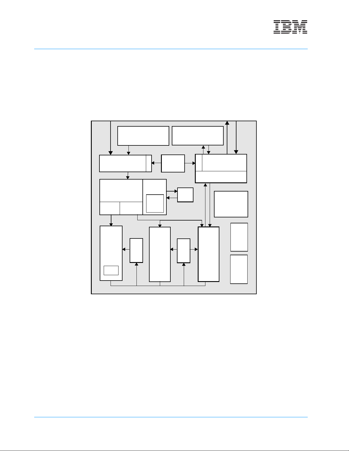
User’s Manual
PPC440x5 CPU Core Preliminary
1.3 PPC440x5 Organization
The PPC440x5 core includes a seven-stage pipelined PowerPC core, which consists of a three stage, dualissue instruction fetch and decode unit with attached branch unit, together with three independent, 4-stage
pipelines for complex integer, simple integer, and load/store operations, respectively. The PPC440x5 core
also includes a memory management unit (MMU); separate instruction and data cache units; JTAG, debug,
and trace logic; and timer facilities.
Figure 1-1 illustrates the logical organization of the PPC440x5 core:
128-bit
PLB
I-Cache Controller
Instruction
Unit
Issue Issue
0
Complex
Integer
Pipe
MAC
Instruction Cache
(Size Configurable)
ITLB
Branch
Unit
Target
Addr
File
Cache
Simple
Integer
Pipe
1
GPR
Data Cache
(Size Configurable)
MMU
64-entry
4KB
BHT
GPR
File
Load/Store Queues
DTLB
D-Cache Controller
DCR Bus
Debug
JTAG
Load
Store
Pipe
Interrupt
Clocks
128-bit
PLB
Trace
and
Timers
and
Pwr Mgmt
Figure 1-1. PPC440 Core Block Diagram
1.3.1 Superscalar Instruction Unit
The instruction unit of the PPC440x5 core fetches, decodes, and issues two instructions per cycle to any
combination of the three execution pipelines and/or the APU interface (see “Execution Pipelines” below, and
Auxiliary Processor Unit (APU) Port on page 36). The instruction unit includes a branch unit which provides
dynamic branch prediction using a branch history table (BHT), as well as a branch target address cache
(BTAC). These mechanisms greatly improve the branch prediction accuracy and reduce the latency of taken
branches, such that the target of a branch can usually be executed immediately after the branch itself, with no
penalty.
overview.fm.
Page 30 of 589
September 12, 2002
Page 31

User’s Manual
Preliminary PPC440x5 CPU Core
1.3.2 Execution Pipelines
The PPC440x5 core contains three execution pipelines: complex integer, simple integer, and load/store.
Each pipeline consists of four stages and can access the nine-ported (six read, three write) GPR file. In order
to improve performance and avoid contention for the GPR file, there are two identical copies of it. One is dedicated to the complex integer pipeline, while the other is shared by the simple integer and the load/store pipelines.
The complex integer pipeline handles all arithmetic, logical, branch, and system management instructions
(such as interrupt and TLB management, move to/from system registers, and so on). This pipeline also
handles multiply and divide operations, and 24 DSP instructions that perform a variety of multiply-accumulate
operations. The complex integer pipeline multiply unit can perform 32-bit × 32-bit multiply operations with
single-cycle throughput and three-cycle latency;16-bit × 32-bit multiply operations have only two-cycle
latency. Divide operations take 33 cycles.
The simple integer pipeline can handle most arithmetic and logical operations which do not update the Condition Register (CR).
The load/store pipeline handles all load, store, and cache management instructions. All misaligned operations are handled in hardware, with no penalty on any operation which is contained within an aligned 16-byte
region. The load/store pipeline supports all operations to both big endian and little endian data regions.
Appendix B, “PPC440x5 Core Compiler Optimizations,” provides detailed information on instruction timings
and performance implications in the PPC440x5 core.
1.3.3 Instruction and Data Cache Controllers
The PPC440x5 core provides separate instruction and data cache controllers and arrays, which allow concurrent access and minimize pipeline stalls. The storage capacity of the cache arrays, which can range from
8KB–32KB each, depends upon the implementation. Both cache controllers have 32-byte lines, and both are
highly-associative, with 64-way set-associativity for 32KB and 16KB sizes, and 32-way set-associativity for
the 8KB size. Both caches support parity checking on the tags and data in the memory arrays, to protect
against soft errors. If a parity error is detected, the CPU will cause a machine check exception.
The PowerPC instruction set provides a rich set of cache management instructions for software-enforced
coherency. The PPC440x5 implementation also provides special debug instructions that can directly read the
tag and data arrays. See Chapter 4, “Instruction and Data Caches,” for detailed information about the instruction and data cache controllers.
The cache controllers connect to the PLB for connection to the IBM CoreConnect system-on-a-chip environment.
1.3.3.1 Instruction Cache Controller (ICC)
The ICC delivers two instructions per cycle to the instruction unit of the PPC440x5 core. The ICC also
handles the execution of the PowerPC instruction cache management instructions for coherency. The ICC
includes a speculative pre-fetch mechanism which can be configured to automatically pre-fetch a burst of up
to three additional lines upon any fetch request which misses in the instruction cache. These speculative prefetches can be abandoned if the instruction execution branches away from the original instruction stream.
overview.fm.
September 12, 2002
Page 31 of 589
Page 32

User’s Manual
PPC440x5 CPU Core Preliminary
The ICC supports cache line locking, at either an 8-line or 16-line granularity, depending on cache size (16line for 32KB, 8-line for 8KB and 16KB). In addition, the notion of a “transient” portion of the cache is
supported, in which the cache can be configured such that only a limited portion is used for instruction cache
lines from memory pages that are designated by a storage attribute from the MMU as being transient in
nature. Such memory pages would contain code which is unlikely to be reused once the processor moves on
to the next series of instruction lines, and thus performance may be improved by preventing each series of
instruction lines from overwriting all of the “regular” code in the instruction cache.
1.3.3.2 Data Cache Controller (DCC)
The DCC handles all load and store data accesses, as well as the PowerPC data cache management instructions. All misaligned accesses are handled in hardware, with those accesses that are contained within a halfline (16 bytes) being handled as a single request. Load and store accesses which cross a 16-byte boundary
are broken into two separate accesses by the hardware.
The DCC interfaces to the APU port to provide direct load/store access to the data cache for APU load and
store operations. Such APU load and store instructions can access up to 16 bytes (one quadword) in a single
cycle.
The data cache can be operated in a store-in (copy-back) or write-through manner, according to the writethrough storage attribute specified for the memory page by the MMU. The DCC also supports both “storewith-allocate” and “store-without-allocate” operations, such that store operations that miss in the data cache
can either “allocate” the line in the cache by reading it in and storing the new data into the cache, or alternatively bypassing the cache on a miss and simply storing the data to memory. This characteristic can also be
specified on a page-by-page basis by a storage attribute in the MMU.
The DCC also supports cache line locking and “transient” data, in the same manner as the ICC (see Instruc-
tion Cache Controller (ICC) on page 31).
The DCC provides extensive load, store, and flush queues, such that up to three outstanding line fills and up
to four outstanding load misses can be pending, and the DCC can continue servicing subsequent load and
store hits in an out-of-order fashion. Store-gathering can also be performed on caching inhibited, writethrough, and “without-allocate” store operations, for up to 16 contiguous bytes. Finally, each cache line has
four separate “dirty” bits (one per doubleword), so that the amount of data flushed on cache line replacement
can be minimized.
1.3.4 Memory Management Unit (MMU)
The PPC440x5 supports a flat, 36-bit (64GB) real (physical) address space. This 36-bit real address is generated by the MMU, as part of the translation process from the 32-bit effective address, which is calculated by
the processor core as an instruction fetch or load/store address.
The MMU provides address translation, access protection, and storage attribute control for embedded applications. The MMU supports demand paged virtual memory and other management schemes that require
precise control of logical to physical address mapping and flexible memory protection. Working with appropriate system level software, the MMU provides the following functions:
• Translation of the 32-bit effective address space into the 36-bit real address space
• Page level read, write, and execute access control
• Storage attributes for cache policy, byte order (endianness), and speculative memory access
• Software control of page replacement strategy
Page 32 of 589
overview.fm.
September 12, 2002
Page 33

User’s Manual
Preliminary PPC440x5 CPU Core
The translation lookaside buffer (TLB) is the primary hardware resource involved in the control of translation,
protection, and storage attributes. It consists of 64 entries, each specifying the various attributes of a given
page of the address space. The TLB is fully-associative; the entry for a given page can be placed anywhere
in the TLB. The TLB tag and data memory arrays are parity protected against soft errors; if a parity error is
detected, the CPU will cause a machine check exception.
Software manages the establishment and replacement of TLB entries. This gives system software significant
flexibility in implementing a custom page replacement strategy. For example, to reduce TLB thrashing or
translation delays, software can reserve several TLB entries for globally accessible static mappings. The
instruction set provides several instructions for managing TLB entries. These instructions are privileged and
the processor must be in supervisor state in order for them to be executed.
The first step in the address translation process is to expand the effective address into a virtual address. This
is done by taking the 32-bit effective address and appending to it an 8-bit Process ID (PID), as well as a 1-bit
“address space” identifier (AS). The PID value is provided by the PID register (see Chapter 5, “Memory
Management”). The AS identifier is provided by the Machine State Register (MSR, see Chapter 6, “Interrupts
and Exceptions,” which contains separate bits for the instruction fetch address space (MSR[IS]) and the data
access address space (MSR[DS]). Together, the 32-bit effective address, the 8-bit PID, and the 1-bit AS form
a 41-bit virtual address. This 41-bit virtual address is then translated into the 36-bit real address using the
TLB.
The MMU divides the address space (whether effective, virtual, or real) into pages. Eight page sizes (1KB,
4KB, 16KB, 64KB, 256KB, 1MB, 16MB, 256MB) are simultaneously supported, such that at any given time
the TLB can contain entries for any combination of page sizes. In order for an address translation to occur, a
valid entry for the page containing the virtual address must be in the TLB. An attempt to access an address
for which no TLB entry exists causes an Instruction (for fetches) or Data (for load/store accesses) TLB Error
exception.
To improve performance, both the instruction cache and the data cache maintain separate “shadow” TLBs.
The instruction shadow TLB (ITLB) contains four entries, while the data shadow TLB (DTLB) contains eight.
These shadow arrays minimize TLB contention between instruction fetch and data load/store operations. The
instruction fetch and data access mechanisms only accessthe main 64-entry unified TLB when a miss occurs
in the respective shadow TLB. The penalty for a miss in either of the shadow TLBs is three cycles. Hardware
manages the replacement and invalidation of both the ITLB and DTLB; no system software action is required.
Each TLB entry provides separate user state and supervisor state read, write, and execute permission
controls for the memory page associated with the entry. If software attempts to access a page for which it
does not have the necessary permission, an Instruction (for fetches) or Data (for load/store accesses)
Storage exception will occur.
Each TLB entry also provides a collection of storage attributes for the associated page. These attributes
control cache policy (such as cachability and write-through as opposed to copy-back behavior), byte order
(big endian as opposed to little endian), and enabling of speculative access for the page. In addition, a set of
four, user-definable storage attributes are provided. These attributes can be used to control various systemlevel behaviors, such as instruction compression using IBM CodePack technology. They can also be configured to control whether data cache lines are allocated upon a store miss, and whether accesses to a given
page should use the “normal” or “transient” portions of the instruction or data cache (see Chapter 4, “Instruction and Data Caches,” for detailed information about these features).
Chapter 5, “Memory Management,” describes the PPC440x5 MMU functions.
overview.fm.
September 12, 2002
Page 33 of 589
Page 34

User’s Manual
PPC440x5 CPU Core Preliminary
1.3.5 Timers
The PPC440x5 contains a Time Base and three timers: a Decrementer (DEC), a Fixed Interval Timer (FIT),
and a Watchdog Timer. The Time Base is a 64-bit counter which gets incremented at a frequency either
equal to the processor core clock rate or as controlled by a separate asynchronous timer clock input to the
core. No interrupt is generated as a result of the Time Base wrapping back to zero.
The DEC is a 32-bit register that is decremented at the same rate at which the Time Base is incremented.
The user loads the DEC register with a value to create the desired interval. When the register is decremented
to zero, a number of actions occur: the DEC stops decrementing, a status bit is set in the Timer Status
Register (TSR), and a Decrementer exception is reported to the interrupt mechanism of the PPC440x5 core.
Optionally, the DEC can be programmed to reload automatically the value contained in the Decrementer
Auto-Reload register (DECAR), after which the DEC resumes decrementing. The Timer Control Register
(TCR) contains the interrupt enable for the Decrementer interrupt.
The FIT generates periodic interrupts based on the transition of a selected bit from the Time Base. Users can
select one of four intervals for the FIT period by setting a control field in the TCR to select the appropriate bit
from the Time Base. When the selected Time Base bit transitions from 0 to 1, a status bit is set in the TSR
and a Fixed Interval Timer exception is reported to the interrupt mechanism of the PPC440x5 core. The FIT
interrupt enable is contained in the TCR.
Similar to the FIT, the Watchdog Timer also generates a periodic interrupt based on the transition of a
selected bit from the Time Base. Users can select one of four intervals for the watchdog period, again by
setting a control field in the TCR to select the appropriate bit from the Time Base. Upon the first transition
from 0 to 1 of the selected Time Base bit, a status bit is set in the TSR and a Watchdog Timer exception is
reported to the interrupt mechanism of the PPC440x5 core. The Watchdog Timer can also be configured to
initiate a hardware reset if a second transition of the selected Time Base bit occurs prior to the first Watchdog
exception being serviced. This capability provides an extra measure of recoverability from potential system
lock-ups.
The timer functions of the PPC440x5 core are more fully described in Chapter 7, “Timer Facilities.”
1.3.6 Debug Facilities
The PPC440x5 debug facilities include debug modes for the various types of debugging used during hardware and software development. Also included are debug events that allow developers to control the debug
process. Debug modes and debug events are controlled using debug registers in the chip. The debug registers are accessed either through software running on the processor, or through the JTAG port.
The debug modes, events, controls, and interfaces provide a powerful combination of debug facilities for
hardware development tools, such as the RISCWatch™ debugger from IBM.
A brief overview of the debug modes and development tool support are provided below. Chapter 8, “Debug
Facilities,” provides detailed information about each debug mode and other debug resources.
1.3.6.1 Debug Modes
The PPC440x5 core supports four debug modes: internal, external, real-time-trace, and debug wait. Each
mode supports a different type of debug tool used in embedded systems development. Internal debug mode
supports software-based ROM monitors, and external debug mode supports a hardware emulator type of
debug. Real-time-trace mode uses the debug facilities to indicate events within a trace of processor execu-
overview.fm.
Page 34 of 589
September 12, 2002
Page 35

User’s Manual
Preliminary PPC440x5 CPU Core
tion in real time. Debug wait mode enables the processor to continue to service real-time critical interrupts
while instruction execution is otherwise stopped for hardware debug. The debug modes are controlled by
Debug Control Register 0 (DBCR0) and the setting of bits in the Machine State Register (MSR).
Internal debug mode supports accessing architected processor resources, setting hardware and software
breakpoints, and monitoring processor status. In internal debug mode, debug events can generate debug
exceptions, which can interrupt normal program flow so that monitor software can collect processor status
and alter processor resources.
Internal debug mode relies on exception-handling software—running on the processor—along with an
external communications path to debug software problems. This mode is used while the processor continues
executing instructions and enables debugging of problems in application or operating system code. Access to
debugger software executing in the processor while in internal debug mode is through a communications port
on the processor board, such as a serial port or ethernet connection.
External debug mode supports stopping, starting, and single-stepping the processor, accessing architected
processor resources, setting hardware and software breakpoints, and monitoring processor status. In
external debug mode, debug events can architecturally “freeze” the processor. While the processor is frozen,
normal instruction execution stops, and the architected processor resources can be accessed and altered
using a debug tool (such as RISCWatch) attached through the JTAG port. This mode is useful for debugging
hardware and low-level control software problems.
1.3.6.2 Development Tool Support
The PPC440x5 provides powerful debug support for a wide range of hardware and software development
tools.
The OS Open real-time operating system debugger is an example of an operating system-aware debugger,
implemented using software traps.
RISCWatch is an example of a development tool that uses the external debug mode, debug events, and the
JTAG port to support hardware and software development and debugging.
The RISCTrace™ feature of RISCWatch is an example of a development tool that uses the real-time trace
capability of the PPC440x5.
1.4 Core Interfaces
Several interfaces to the PPC440x5 core support the IBM CoreConnect on-chip system architecture, which
simplifies the attachment of on-chip devices. These interfaces include:
• Processor local bus (PLB)
• Device configuration register (DCR) interface
• Auxiliary processor unit (APU) port
• JTAG, debug, and trace ports
• Interrupt interface
• Clock and power management interface
Several of these interfaces are described briefly in the sections below.
overview.fm.
September 12, 2002
Page 35 of 589
Page 36

User’s Manual
PPC440x5 CPU Core Preliminary
1.4.1 Processor Local Bus (PLB)
There are three independent 128-bit PLB interfaces to the PPC440x5 core. Each of these interfaces includes
a 36-bit address bus and a 128-bit data bus. One PLB interface supports instruction cache reads, while the
other two support data cache reads and writes, respectively. The frequency of each PLB interface can be
independently specified, allowing an IBM CoreConnect system in which the interfaces are not all connected
as part of the same PLB and in which each PLB subsystem operates at its own frequency. Each PLB interface frequency can be configured to any value such that the ratio of the processor core frequency to the PLB
(core:PLB) is n:1, n:2, or n:3, where n is any integer greater than or equal to the denominator of the ratio.
Each of the PLB interfaces supports connection to a PLB subsystem of either 32, 64, or 128 bits. The instruction and data cache controllers handle any dynamic data bus resizing which is required when the subsystem
data width is less than the 128 bits of the PPC440x5 core PLB interfaces.
The data cache PLB interfaces make requests for 32-byte lines, as well as for 1 - 15 bytes within a 16-byte
(quadword) aligned region. A 16-byte line request is used for quadword APU load operations to caching
inhibited pages, and for quadword APU store operations to caching inhibited, write-through, or “without allocate” pages.
The instruction cache controller makes 32-byte line read requests, and also presents quadword burst read
requests for up to three 32-byte lines (six quadwords), as part of its speculative line fill mechanism.
Each of the PLB interfaces fully supports the address pipelining capabilities of the PLB, and in fact can go
beyond the pipeline depth and minimum latency which the PLB supports. Specifically, each interface
supports up to three pipelined request/acknowledge sequences prior to performing the data transfers associated with the first request. For the data cache, if each of the requests must themselves be broken into three
separate transactions (for example, for a misaligned doubleword request to a 32-bit PLB slave), then the
interface actually supports up to nine outstanding request/acknowledge sequences prior to the first data
transfer. Furthermore, each PLB interface tolerates a zero-cycle latency between the request and the
address and data acknowledge (that is, the request, address acknowledge, and data acknowledge may all
occur in the same cycle).
1.4.2 Device Control Register (DCR) Interface
The DCR interface provides a mechanism for the PPC440x5 core to setup other on-chip facilities. For
example, programmable resources in an external bus interface unit may be configured for usage with various
memory devices according to their transfer characteristics and address assignments. DCRs are accessed
through the use of the PowerPC mfdcr and mtdcr instructions.
The interface is interlocked with control signals such that it may be connected to peripheral units that may be
clocked at different frequencies from the processor core. The design allows for future expansion of the noncore facilities without changing the I/O on either the PPC440x5 core or the ASIC peripherals.
The DCR interface also allows the PPC440x5 core to communicate with peripheral devices without using the
PLB interface, thereby avoiding the impact to the primary system bus bandwidth, and without additional
segmentation of the useable address map.
1.4.3 Auxiliary Processor Unit (APU) Port
This interface provides the PPC440x5 core with the flexibility for attaching a tightly-coupled coprocessor-type
macro incorporating instructions which go beyond those provided within the processor core itself. The APU
port provides sufficient functionality for attachment of various coprocessor functions such as a fully-compliant
overview.fm.
Page 36 of 589
September 12, 2002
Page 37

User’s Manual
Preliminary PPC440x5 CPU Core
PowerPC floating point unit (single or double precision), multimedia engine, DSP, or other custom function
implementing algorithms appropriate for specific system applications. The APU interface supports dual-issue
pipeline designs, and can be used with macros that contain their own register files, or with simpler macros
which use the CPU GPR file for source and/or target operands. APU load and store instructions can directly
access the PPC440x5 data cache, with operands of up to a quadword (16 bytes) in length.
The APU interface provides the capability for a coprocessor to execute concurrently with the PPC440x5 core
instructions that are not part of the PowerPC instruction set. Accordingly, areas have been reserved within
the architected instruction space to allow for these customer-specific or application-specific APU instruction
set extensions.
1.4.4 JTAG Port
The PPC440x5 JTAG port is enhanced to support the attachment of a debug tool such as the RISCWatch
product from IBM. Through the JTAG test access port, and using the debug facilities designed into the
PPC440x5 core, a debug workstation can single-step the processor and interrogate internal processor state
to facilitate hardware and software debugging. The enhancements comply with the IEEE 1149.1 specification
for vendor-specific extensions, and are therefore compatible with standard JTAG hardware for boundaryscan system testing.
overview.fm.
September 12, 2002
Page 37 of 589
Page 38

User’s Manual
PPC440x5 CPU Core Preliminary
Page 38 of 589
overview.fm.
September 12, 2002
Page 39

User’s Manual
Preliminary PPC440x5 CPU Core
2. Programming Model
The programming model of the PPC440x5 core describes how the following features and operations of the
core appear to programmers:
• Storage addressing (including data types and byte ordering), starting on page 39
• Registers, starting on page 47
• Instruction classes, starting on page 53
• Instruction set, starting on page 56
• Branch processing, starting on page 64
• Integer processing, starting on page 71
• Processor control, starting on page 74
• User and supervisor state, starting on page 80
• Speculative access, starting on page 81
• Synchronization, starting on page 82
2.1 Storage Addressing
As a 32-bit implementation of the Book-E Enhanced PowerPC Architecture, the PPC440x5 core implements
a uniform 32-bit effective address (EA) space. Effective addresses are expanded into virtual addresses and
then translated to 36-bit (64GB) real addresses by the memory management unit (see Memory Management
on page 133 for more information on the translation process). The organization of the real address space into
a physical address space is system-dependent, and is described in the user’s manuals for chip-level products
that incorporate a PPC440x5 core.
The PPC440x5 generates an effective address whenever it executes a storage access, branch, cache
management, or translation lookaside buffer (TLB) management instruction, or when it fetches the next
sequential instruction.
2.1.1 Storage Operands
Bytes in storage are numbered consecutively starting with 0. Each number is the address of the corresponding byte.
Data storage operands accessed by the integer load/store instructions may be bytes, halfwords, words, or—
for load/store multiple and string instructions—a sequence of words or bytes, respectively. Data storage operands accessed by auxiliary processor (AP) load/store instructions can be bytes, halfwords, words, doublewords, or quadwords. The address of a storage operand is the address of its first byte (that is, of its lowestnumbered byte). Byte ordering can be either big endian or little endian, as controlled by the endian storage
attribute (see Byte Ordering on page 42; also see Endian (E) on page 146 for more information on the endian
storage attribute).
Operand length is implicit for each scalar storage access instruction type (that is, each storage access
instruction type other than the load/store multiple and string instructions). The operand of such a scalar
storage access instruction has a “natural” alignment boundary equal to the operand length. In other words,
the ‘natural’ address of an operand is an integral multiple of the operand length. A storage operand is said to
be aligned if it is aligned at its natural boundary: otherwise it is said to be unaligned.
prgmodel.fm.
September 12, 2002
Page 39 of 589
Page 40

User’s Manual
PPC440x5 CPU Core Preliminary
Data storage operands for storage access instructions have the following characteristics.
Table 2-1. Data Operand Definitions
Storage Access Instruction
Type
Byte (or String) 8 bits 0bxxxx
Halfword 2 bytes 0bxxx0
Word (or Multiple) 4 bytes 0bxx00
Doubleword (AP only) 8 bytes 0bx000
Quadword (AP only) 16 bytes 0b0000
Operand
Length
Addr[28:31] if aligned
Note: An “x” in an address bit position indicates that the bit can be 0
or 1 independent of the state of other bits in the address.
The alignment of the operand effective address of some storage access instructions may affect performance,
and in some cases may cause an Alignment exception to occur. For such storage access instructions, the
best performance is obtained when the storage operands are aligned. Table 2-2 summarizes the effects of
alignment on those storage access instruction types for which such effects exist. If an instruction type is not
shown in the table, then there are no alignment effects for that instruction type.
Table 2-2. Alignment Effects for Storage Access Instructions
Storage Access
InstructionType
Integer load/store halfword
Integer load/store word
Integer load/store multiple or string
AP load/store halfword
AP load/store word
AP load/store doubleword
AP load/store quadword
Broken into two byte accesses if crosses 16-byte boundary (EA[28:31] = 0b1111); otherwise
no effect
Broken into two accesses if crosses 16-byte boundary (EA[28:31] > 0b1100); otherwise no
effect
Broken into a series of 4-byte accesses untilthe last byte is accessed or a 16-byte boundary is
reached, whichever occurs first. If bytes remain past a 16-byte boundary, resume accessing 4
bytes at a time until the last byte is accessed or the next 16-byte boundary is reached, whichever occurs first; repeat.
Alignment exception if crosses 16-byte boundary (EA[28:31] = 0b1111); otherwise no effect
(see note)
Alignment exception if crosses 16-byte boundary (EA[28:31] > 0b1100); otherwise no effect
(see note)
Alignment exception if crosses 16-byte boundary (EA[28:31] > 0b1000); otherwise no effect
(see note)
Alignment exception if crosses 16-byte boundary (EA[28:31] ≠ 0b0000); otherwise no effect
Alignment Effects
Note: An auxiliary processor can specify that the EA for a givenAP load/store instruction must be aligned at the
operand-size boundary, or alternatively, at a word boundary.If the AP so indicates this requirement and the
calculated EA fails to meet it, the PPC440x5 core generates an Alignment exception. Alternatively, an
auxiliary processor can specify that the EA for a given AP load/store instruction should be “forced” to be
aligned, by ignoring the appropriate number of low-order EA bits and processing the AP load/store as if
those bits were 0. Byte, halfword, word, doubleword,andquadwordAP load/store instructions would ignore
0, 1, 2, 3, and 4 low-order EA bits, respectively.
Cache management instructions access cache block operands, and for the PPC440x5 core the cache block
size is 32 bytes. However, the effective addresses calculated by cache management instructions are not
required to be aligned on cache block boundaries. Instead, the architecture specifies that the associated loworder effective address bits (bits 27:31 for PPC440x5) are ignored during the execution of these instructions.
prgmodel.fm.
Page 40 of 589
September 12, 2002
Page 41

User’s Manual
Preliminary PPC440x5 CPU Core
Similarly, the TLB management instructions access page operands, and—as determined by the page size—
the associated low-order effective address bits are ignored during the execution of these instructions.
Instruction storage operands, on the other hand, are always four bytes long, and the effective addresses
calculated by Branch instructions are therefore always word-aligned.
2.1.2 Effective Address Calculation
For a storage access instruction, if the sum of the effective address and the operand length exceeds the
maximum effective address of 232–1 (that is, the storage operand itself crosses the maximum address
boundary), the result of the operation is undefined, as specified by the architecture. The PPC440x5 core
performs the operation as if the storage operand wrapped around from the maximum effective address to
effective address 0. Software, however, should not depend upon this behavior, so that it may be ported to
other implementations that do not handle this scenario in the same fashion. Accordingly, software should
ensure that no data storage operands cross the maximum address boundary.
Note that since instructions are words and since the effective addresses of instructions are always implicitly
on word boundaries, it is not possible for an instruction storage operand to cross any word boundary,
including the maximum address boundary.
Effective address arithmetic, which calculates the starting address for storage operands, wraps around from
the maximum address to address 0, for all effective address computations except next sequential instruction
fetching. See Instruction Storage Addressing Modes on page 41 for more information on next sequential
instruction fetching at the maximum address boundary.
2.1.2.1 Data Storage Addressing Modes
There are two data storage addressing modes supported by the PPC440x5 core:
• Base + displacement (D-mode) addressing mode:
The 16-bit D field is sign-extended and added to the contents of the GPR designated by RA or to zero if
RA = 0; the low-order 32 bits of the sum form the effective address of the data storage operand.
• Base + index (X-mode) addressing mode:
The contents of the GPR designated by RB (or the value 0 for lswi and stswi) are added to the contents
of the GPR designated by RA, or to 0 if RA = 0; the low-order 32 bits of the sum form the effective
address of the data storage operand.
2.1.2.2 Instruction Storage Addressing Modes
There are four instruction storage addressing modes supported by the PPC440x5 core:
• I-form branch instructions (unconditional):
The 24-bit LI field is concatenated on the right with 0b00, sign-extended, and then added to either the
address of the branch instruction if AA=0, or to 0 if AA=1; the low-order 32 bits of the sum form the effective address of the next instruction.
• Taken B-form branch instructions:
prgmodel.fm.
September 12, 2002
Page 41 of 589
Page 42

User’s Manual
PPC440x5 CPU Core Preliminary
The 14-bit BD field is concatenated on the right with 0b00, sign-extended, and then added to either the
address of the branch instruction if AA=0, or to 0 if AA=1; the low-order 32 bits of the sum form the effective address of the next instruction.
• Taken XL-form branch instructions:
The contents of bits 0:29 of the Link Register (LR) or the Count Register (CTR) are concatenated on the
right with 0b00 to form the 32-bit effective address of the next instruction.
• Next sequential instruction fetching (including non-taken branch instructions):
The value 4 is added to the address of the current instruction to form the 32-bit effective address of the
next instruction. If the address of the current instruction is 0xFFFFFFFC, the PPC440x5 core wraps the
next sequential instruction address back to address 0. This behavior is not required by the architecture,
which specifies that the next sequential instruction address is undefined under these circumstances.
Therefore, software should not depend upon this behavior, so that it may be ported to other implementations that do not handle this scenario in the same fashion. Accordingly, if software wishes to execute
across this maximum address boundary and wrap back to address 0, it should place an unconditional
branch at the boundary, with a displacement of 4.
In addition to the above four instruction storage addressing modes, the following behavior applies to
branch instructions:
• Any branch instruction with LK=1:
The value 4 is added to the address of the current instruction and the low-order 32 bits of the result are
placed into the LR. As for the similar scenario for next sequential instruction fetching, if the address of the
branch instruction is 0xFFFF FFFC, the result placed into the LR is architecturally undefined, although
once again the PPC440x5 core wraps the LR update value back to address 0. Again, however, software
should not depend on this behavior, in order that it may be ported to implementations which do not handle this scenario in the same fashion.
2.1.3 Byte Ordering
If scalars (individual data items and instructions) were indivisible, there would be no such concept as “byte
ordering.” It is meaningless to consider the order of bits or groups of bits within the smallest addressable unit
of storage, because nothing can be observed about such order. Only when scalars, which the programmer
and processor regard as indivisible quantities, can comprise more than one addressable unit of storage does
the question of order arise.
For a machine in which the smallest addressable unit of storage is the 64-bit doubleword, there is no question
of the ordering of bytes within doublewords. All transfers of individual scalars between registers and storage
are of doublewords, and the address of the byte containing the high-order eight bits of a scalar is no different
from the address of a byte containing any other part of the scalar.
For the Book-E Enhanced PowerPC Architecture, as for most current computer architectures, the smallest
addressable unit of storage is the 8-bit byte. Many scalars are halfwords, words, or doublewords, which
consist of groups of bytes. When a word-length scalar is moved from a register to storage, the scalar occupies four consecutive byte addresses. It thus becomes meaningful to discuss the order of the byte addresses
with respect to the value of the scalar: which byte contains the highest-order eight bits of the scalar, which
byte contains the next-highest-order eight bits, and so on.
Given a scalar that contains multiple bytes, the choice of byte ordering is essentially arbitrary. There are 4! =
24 ways to specify the ordering of four bytes within a word, but only two of these orderings are sensible:
prgmodel.fm.
Page 42 of 589
September 12, 2002
Page 43

User’s Manual
Preliminary PPC440x5 CPU Core
• The ordering that assigns the lowest address to the highest-order (“left-most”) eight bits of the scalar, the
next sequential address to the next-highest-order eight bits, and so on.
This ordering is called big endian because the “big end” (most-significant end) of the scalar, considered
as a binary number, comes first in storage. IBM RISC System/6000, IBM System/390, and Motorola
680x0 are examples of computer architectures using this byte ordering.
• The ordering that assigns the lowest address to the lowest-order (“right-most”) eight bits of the scalar, the
next sequential address to the next-lowest-order eight bits, and so on.
This ordering is called little endian because the “little end” (least-significant end) of the scalar, considered
as a binary number, comes first in storage. The Intel x86 is an example of a processor architecture using
this byte ordering.
PowerPC Book-E supports both big endian and little endian byte ordering, for both instruction and data
storage accesses. Which byte ordering is used is controlled on a memory page basis by the endian (E)
storage attribute, which is a field within the TLB entry for the page. The endian storage attribute is set to 0 for
a big endian page, and is set to 1 for a little endian page. See Memory Management on page 133 for more
information on memory pages, the TLB, and storage attributes, including the endian storage attribute.
2.1.3.1 Structure Mapping Examples
The following C language structure, s, contains an assortment of scalars and a character string. The
comments show the value assumed to be in each structure element; these values show how the bytes
comprising each structure element are mapped into storage.
struct {
int a; /* 0x1112_1314 word */
long long b; /* 0x2122_2324_2526_2728 doubleword */
char *c; /* 0x3132_3334 word */
char d[7]; /* 'A','B','C','D','E','F','G' array of bytes */
short e; /* 0x5152 halfword */
int f; /* 0x6162_6364 word */
} s;
C structure mapping rules permit the use of padding (skipped bytes) to align scalars on desirable boundaries.
The structure mapping examples below show each scalar aligned at its natural boundary. This alignment
introduces padding of four bytes between a and b, one byte between d and e, and two bytes between e and
f. The same amount of padding is present in both big endian and little endian mappings.
prgmodel.fm.
September 12, 2002
Page 43 of 589
Page 44

User’s Manual
PPC440x5 CPU Core Preliminary
Big Endian Mapping
The big endian mapping of structure s follows (the data is highlighted in the structure mappings). Addresses,
in hexadecimal, are below the data stored at the address. The contents of each byte, as defined in structure
s, is shown as a (hexadecimal) number or character (for the string elements). The shaded cells correspond to
padded bytes.
11 12 13 14
0x00 0x01 0x02 0x03 0x04 0x05 0x06 0x07
21 22 23 24 25 26 27 28
0x08 0x09 0x0A 0x0B 0x0C 0x0D 0x0E 0x0F
31 32 33 34 'A' 'B' 'C' 'D'
0x10 0x11 0x12 0x13 0x14 0x15 0x16 0x17
'E' 'F' 'G' 51 52
0x18 0x19 0x1A 0x1B 0x1C 0x1D 0x1E 0x1F
61 62 63 64
0x20 0x21 0x22 0x23 0x24 0x25 0x26 0x27
Little Endian Mapping
Structure
s is shown mapped little endian.
14 13 12 11
0x00 0x01 0x02 0x03 0x04 0x05 0x06 0x07
28 27 26 25 24 23 22 21
0x08 0x09 0x0A 0x0B 0x0C 0x0D 0x0E 0x0F
34 33 32 31 'A' 'B' 'C' 'D'
0x10 0x11 0x12 0x13 0x14 0x15 0x16 0x17
'E' 'F' 'G' 52 51
0x18 0x19 0x1A 0x1B 0x1C 0x1D 0x1E 0x1F
64 63 62 61
0x20 0x21 0x22 0x23 0x24 0x25 0x26 0x27
2.1.3.2 Instruction Byte Ordering
PowerPC Book-E defines instructions as aligned words (four bytes) in memory. As such, instructions in a big
endian program image are arranged with the most-significant byte (MSB) of the instruction word at the
lowest-numbered address.
Consider the big endian mapping of instruction p at address 0x00, where, for example, p = add r7, r7, r4:
Page 44 of 589
MSB LSB
0x00 0x01 0x02 0x03
prgmodel.fm.
September 12, 2002
Page 45

User’s Manual
Preliminary PPC440x5 CPU Core
On the other hand, in a little endian mapping the same instruction is arranged with the least-significant byte
(LSB) of the instruction word at the lowest-numbered address:
LSB MSB
0x00 0x01 0x02 0x03
By the definition of PowerPC Book-E bit numbering, the most-significant byte of an instruction is the byte
containing bits 0:7 of the instruction. As depicted in the instruction format diagrams (see Instruction Formats
on page 250), this most-significant byte is the one which contains the primary opcode field (bits 0:5). Due to
this difference in byte orderings, the processor must perform whatever byte reversal is required (depending
on the particular byte ordering in use) in order to correctly deliver the opcode field to the instruction decoder.
In the PPC440x5, this reversal is performed between the memory interface and the instruction cache,
according to the value of the endian storage attribute for each memory page, such that the bytes in the
instruction cache are always correctly arranged for delivery directly to the instruction decoder.
If the endian storage attribute for a memory page is reprogrammed from one byte ordering to the other, the
contents of the memory page must be reloaded with program and data structures that are in the appropriate
byte ordering. Furthermore, anytime the contents of instruction memory change, the instruction cache must
be made coherent with the updates by invalidating the instruction cache and refetching the updated memory
contents with the new byte ordering.
2.1.3.3 Data Byte Ordering
Unlike instruction fetches, data accesses cannot be byte-reversed between memory and the data cache.
Data byte ordering in memory depends upon the data type (byte, halfword, word, and so on) of a specific data
item. It is only when moving a data item of a specific type from or to an architected register (as directed by the
execution of a particular storage access instruction) that it becomes known what kind of byte reversal may be
required due to the byte ordering of the memory page containing the data item. Therefore, byte reversal
during load or store accesses is performed between data cache (or memory, on a data cache miss, for
example) and the load register target or store register source, depending on the specific type of load or store
instruction (that is, byte, halfword, word, and so on).
Comparing the big endian and little endian mappings of structure s, as shown in Structure Mapping Examples
on page 43, the differences between the byte locations of any data item in the structure depends upon the
size of the particular data item. For example (again referring to the big endian and little endian mappings of
structure s):
• The word a has its four bytes reversed within the word spanning addresses 0x00 – 0x03.
• The halfword e has its two bytes reversed within the halfword spanning addresses 0x1C – 0x1D.
Note that the array of bytes d, where each data item is a byte, is not reversed when the big endian and little
endian mappings are compared. For example, the character 'A' is located at address 0x14 in both the big
endian and little endian mappings.
The size of the data item being loaded or stored must be known before the processor can decide whether,
and if so, how to reorder the bytes when moving them between a register and the data cache (or memory).
• For byte loads and stores, including strings, no reordering of bytes occurs, regardless of byte ordering.
• For halfword loads and stores, bytes are reversed within the halfword, for one byte order with respect to
the other.
prgmodel.fm.
September 12, 2002
Page 45 of 589
Page 46

User’s Manual
PPC440x5 CPU Core Preliminary
• For word loads and stores (including load/store multiple), bytes are reversed within the word, for one byte
order with respect to the other.
• For doubleword loads and stores (AP loads/stores only), bytes are reversed within the doubleword, for
one byte order with respect to the other.
• For quadword loads and stores (AP loads/stores only), bytes are reversed within the quadword, for one
byte order with respect to the other.
Note that this mechanism applies independent of the alignment of data. In other words, when loading a multibyte data operand with a scalar load instruction, bytes are accessed from the data cache (or memory) starting
with the byte at the calculated effective address and continuing with consecutively higher-numbered bytes
until the required number of bytes have been retrieved. Then, the bytes are arranged such that either the byte
from the highest-numbered address (for big endian storage regions) or the lowest-numbered address (for
little endian storage regions) is placed into the least-significant byte of the register. The rest of the register is
filled in corresponding order with the rest of the accessed bytes. An analogous procedure is followed for
scalar store instructions.
For load/store multiple instructions, each group of four bytes is transferred between memory and the register
according to the procedure for a scalar load word instruction.
For load/store string instructions, the most-significant byte of the first register is transferred to or frommemory
at the starting (lowest-numbered) effective address, regardless of byte ordering. Subsequent register bytes
(from most-significant to least-significant, and then moving into the next register, starting with the most-significant byte, and so on) are transferred to or from memory at sequentially higher-numbered addresses. This
behavior for byte strings ensures that if two strings are loaded into registers and then compared, the first
bytes of the strings are treated as most significant with respect to the comparison.
2.1.3.4 Byte-Reverse Instructions
PowerPC Book-E defines load/store byte-reverse instructions which can access storage which is specified as
being of one byte ordering in the same manner that a regular (that is, non-byte-reverse) load/store instruction
would access storage which is specified as being of the opposite byte ordering. In other words, a load/store
byte-reverse instruction to a big endian memory page transfers data between the data cache (or memory)
and the register in the same manner that a normal load/store would transfer the data to or from a little endian
memory page. Similarly, a load/store byte-reverse instruction to a little endian memory page transfers data
between the data cache (or memory) and the register in the same manner that a normal load/store would
transfer the data to or from a big endian memory page.
The function of the load/store byte-reverse instructions is useful when a particular memory page contains a
combination of data with both big endian and little endian byte ordering. In such an environment, the Endian
storage attribute for the memory page would be set according to the predominant byte ordering for the page,
and the normal load/store instructions would be used to access data operands which used this predominant
byte ordering. Conversely, the load/store byte-reverse instructions would be used to access the data operands which were of the other (less prevalent) byte ordering.
Software compilers cannot typically make general use of the load/store byte-reverse instructions, so they are
ordinarily used only in special, hand-coded device drivers.
Page 46 of 589
prgmodel.fm.
September 12, 2002
Page 47

User’s Manual
Preliminary PPC440x5 CPU Core
2.2 Registers
This section provides an overview of the register categories and types provided by the PPC440x5. Detailed
descriptions of each of the registers are provided within the chapters covering the functions with which they
are associated (for example, the cache control and cache debug registers are described in Instruction and
Data Caches on page 95). An alphabetical summary of all registers, including bit definitions, is provided in
Register Summary on page 451
All registers in the PPC440x5 core are architected as 32 bits wide, although certain bits in some registers are
reserved and thus not necessarily implemented. For all registers with fields marked as reserved, these
reserved fields should be written as 0 and read as undefined. The recommended coding practice is to
perform the initial write to a register with reserved fields set to 0, and to perform all subsequent writes to the
register using a read-modify-write strategy: read the register; use logical instructions to alter defined fields,
leaving reserved fields unmodified; and write the register.
All of the registers are grouped into categories according to the processor functions with which they are associated. In addition, each register is classified as being of a particular type, as characterized by the specific
instructions which are used to read and write registers of that type. Finally, most of the registers contained
within the PPC440x5 core are defined by the Book-E Enhanced PowerPC Architecture, although some registers are implementation-specific and unique to the PPC440x5.
Figure 2-1 on page 48 illustrates the PPC440x5 registers contained in the user programming model, that is,
those registers to which access is non-privileged and which are available to both user and supervisor
programs. Figure 2-2 on page 49 illustrates the PPC440x5 registers contained in the supervisor programming model, to which access is privileged and which are available to supervisor programs only. See User and
Supervisor Modes on page 80 for more information on privileged instructions and register access, and the
user and supervisor programming models.
Table 2-3 on page 50, lists each register category and the registers that belong to each category, along with
their types and a cross-reference to the section of this document which describes them more fully. Registers
that are not part of PowerPC Book-E, and are thus specific to the PPC440x5, are shown in italics in
Table 2-3. Unless otherwise indicated, all registers have read/write access.
prgmodel.fm.
September 12, 2002
Page 47 of 589
Page 48

User’s Manual
PPC440x5 CPU Core Preliminary
Integer Processing
General Purpose
GPR0
GPR1
GPR2
•
•
•
GPR31
Integer Exception Register
XER
Timer
Time Base
TBL
TBU
Branch Control
Condition Register
CR
Count Register
CTR
Link Register
LR
Processor Control
SPR General 4–7
SPRG4
SPRG5
SPRG5
SPRG7
User SPR General 0
USPRG0
Figure 2-1. User Programming Model Registers
Page 48 of 589
prgmodel.fm.
September 12, 2002
Page 49

User’s Manual
Preliminary PPC440x5 CPU Core
Processor Control
Machine State Register
MSR
Processor Version Register
PVR
Processor ID Register
PIR
Core Configuration Registers
CCR0
CCR1
Reset Configuration
RSTCFG
SPR General
SPRG0
•
•
•
SPRG7
Interrupt Processing
Exception Syndrome Register
ESR
Machine Check Syndrome Register
MCSR
Data Exception Address Register
DEAR
Save/Restore Registers
SRR0
SRR1
Critical Save/Restore Registers
CSRR0
CSRR1
Machine Check Save/Restore Registers
MCSRR0
MCSRR1
Interrupt Vector Prefix Register
IVPR
Interrupt Vector Offset Registers
IVOR0
•
•
•
IVOR15
Timer
Time Base
TBU
TBL
Timer Control Register
TCR
Timer Status Register
TSR
Decrementer
DEC
Decrementer Auto-Reload
DECAR
Cache Control
Instruction Cache Victim Limit
IVLIM
Instruction Cache Normal Victim
INV0
INV1
INV2
INV3
Instruction Cache Transient Victim
ITV0
ITV1
ITV2
ITV3
Data Cache Victim Limit
DVLIM
Data Cache Normal Victim
DNV0
DNV1
DNV2
DNV3
Data Cache Transient Victim
DTV0
DTV1
DTV2
DTV3
Storage Control
Process ID
PID
MMU Control Register
MMUCR
Debug
Debug Status Register
DBSR
Debug Data Register
DBDR
Debug Control Registers
DBCR0
DBCR1
DBCR2
Data Address Compares
DAC1
DAC2
Data Value Compares
DVC1
DVC2
Instruction Address Compares
IAC1
IAC2
IAC3
IAC4
Cache Debug
Instruction Cache Debug Data Register
ICDBDR
Instruction Cache Debug Tag Registers
ICDBTRH
ICDBTRL
Data Cache Debug Tag Registers
DCDBTRH
DCDBTRL
prgmodel.fm.
September 12, 2002
Figure 2-2. Supervisor Programming Model Registers
Page 49 of 589
Page 50

User’s Manual
PPC440x5 CPU Core Preliminary
Table 2-3. Register Categories
Register Category Register(s) Model and Access Type Page
CR User CR 67
Branch Control
Cache Control
Cache Debug
Debug
Device Control
Integer Processing
Interrupt Processing
Processor Control
Storage Control
CTR User SPR 67
LR User SPR 66
DNV0–DNV3 Supervisor SPR 97
DTV0–DTV3 Supervisor SPR 97
DVLIM Supervisor SPR 99
INV0–INV3 Supervisor SPR 97
ITV0–ITV3 Supervisor SPR 97
IVLIM Supervisor SPR 99
DCDBTRH, DCDBTRL Supervisor, read-only SPR 127
ICDBDR, ICDBTRH, ICDBTRL
DAC1–DAC2 Supervisor SPR 246
DBCR0–DBCR2 Supervisor SPR 239
DBDR Supervisor SPR 247
DBSR Supervisor SPR 244
DVC1–DVC2 Supervisor SPR 246
IAC1–IAC4 Supervisor SPR 245
Implemented outside core Supervisor DCR 53
GPR0–GPR31 User GPR 71
XER User SPR 72
CSRR0–CSRR1 Supervisor SPR 168
DEAR Supervisor SPR 170
ESR Supervisor SPR 172
IVOR0–IVOR15 Supervisor SPR 170
IVPR Supervisor SPR 171
MCSR Supervisor SPR 174
MCSRR0-MCSRR1 Supervisor SPR 169
SRR0–SRR1 Supervisor SPR 167
CCR0 Supervisor SPR 108
CCR1 Supervisor SPR 108
MSR Supervisor MSR 165
PIR, PVR Supervisor, read-only SPR 75
RSTCFG Supervisor, read-only SPR 79
SPRG0–SPRG3 Supervisor SPR 75
SPRG4–SPRG7 User, read-only; Supervisor SPR 75
USPRG0 User SPR 75
MMUCR Supervisor SPR 148
PID Supervisor SPR 151
Supervisor, read-only SPR 112
Page 50 of 589
prgmodel.fm.
September 12, 2002
Page 51

User’s Manual
Preliminary PPC440x5 CPU Core
Table 2-3. Register Categories
Register Category Register(s) Model and Access Type Page
DEC Supervisor SPR 211
DECAR Supervisor, write-only SPR 211
TBL, TBU User read, Supervisor write SPR 209
Timer
TCR Supervisor SPR 215
TSR Supervisor SPR 216
prgmodel.fm.
September 12, 2002
Page 51 of 589
Page 52

User’s Manual
PPC440x5 CPU Core Preliminary
2.2.1 Register Types
There are five register types contained within and/or supported by the PPC440x5 core. Each register type is
characterized by the instructions which are used to read and write the registers of that type. The following
subsections provide an overview of each of the register types and the instructions associated with them.
2.2.1.1 General Purpose Registers
The PPC440x5 core contains 32 integer general purpose registers (GPRs); each contains 32 bits. Data from
the data cache or memory can be loaded into GPRs using integer load instructions; the contents of GPRs can
be stored to the data cache or memory using integer store instructions. Most of the integer instructions reference GPRs. The GPRs are also used as targets and sources for most of the instructions which read and write
the other register types.
Integer Processing on page 71 provides more information on integer operations and the use of GPRs.
2.2.1.2 Special Purpose Registers
Special Purpose Registers (SPRs) are directly accessed using the
mtspr and mfspr instructions. In addi-
tion, certain SPRs may be updated as a side-effect of the execution of various instructions. For example, the
Integer Exception Register (XER) (see Integer Exception Register (XER) on page 72) is an SPR which is
updated with arithmetic status (such as carry and overflow) upon execution of certain forms of integer arithmetic instructions.
SPRs control the use of the debug facilities, timers, interrupts, memory management, caches, and other
architected processor resources. Table 10-2 on page 454 shows the mnemonic, name, and number for each
SPR, in order by SPR number. Each of the SPRs is described in more detail within the section or chapter
covering the function with which it is associated. See Table 2-3 on page 50 for a cross-reference to the associated document section for each register.
2.2.1.3 Condition Register
The Condition Register (CR) is a 32-bit register of its own unique type and is divided up into eight, independent 4-bit fields (CR0–CR7). The CR may be used to record certain conditional results of various arithmetic
and logical operations. Subsequently, conditional branch instructions may designate a bit of the CR as one of
the branch conditions (see Branch Processing on page 64). Instructions are also provided for performing
logical bit operations and for moving fields within the CR.
See Condition Register (CR) on page 67 for more information on the various instructions which can update
the CR.
Page 52 of 589
prgmodel.fm.
September 12, 2002
Page 53

User’s Manual
Preliminary PPC440x5 CPU Core
2.2.1.4 Machine State Register
The Machine State Register (MSR) is a register of its own unique type that controls important chip functions,
such as the enabling or disabling of various interrupt types.
The MSR can be written from a GPR using the
a GPR using the
mfmsr instruction. The MSR[EE] bit can be set or cleared atomically using the wrtee or
mtmsr instruction. The contents of the MSR can be read into
wrteei instructions. The MSR contents are also automatically saved, altered, and restored by the interrupt-
handling mechanism. See Machine State Register (MSR) on page 165 for more detailed information on the
MSR and the function of each of its bits.
2.2.1.5 Device Control Registers
Device Control Registers (DCRs) are on-chip registers that exist architecturally and physically outside the
PPC440x5 core, and thus are not specified by the Book-E Enhanced PowerPC Architecture, nor by this
user’s manual for the PPC440x5 core. Rather, PowerPC Book-E simply defines the existence of the DCR
address space and the instructions that access the DCRs, and does not define any particular DCRs. The
DCR access instructions are mtdcr (move to device control register) and mfdcr (move from device control
register), which move data between GPRs and the DCRs.
DCRs may be used to control various on-chip system functions, such as the operation of on-chip buses,
peripherals, and certain processor core behaviors.
2.3 Instruction Classes
PowerPC Book-E architecture defines all instructions as falling into exactly one of the following four classes,
as determined by the primary opcode (and the extended opcode, if any):
1. Defined
2. Allocated
3. Preserved
4. Reserved (-illegal or -nop)
2.3.1 Defined Instruction Class
This class of instructions consists of all the instructions defined in PowerPC Book-E. In general, defined
instructions are guaranteed to be supported within a PowerPC Book-E system as specified by the architecture, either within the processor implementation itself or within emulation software supported by the system
operating software.
One exception to this is that, for implementations (such as the PPC440x5) that only provide the 32-bit subset
of PowerPC Book-E, it is not expected (and likely not even possible) that emulation of the 64-bit behavior of
the defined instructions will be provided by the system.
As defined by PowerPC Book-E, any attempt to execute a defined instruction will:
• cause an Illegal Instruction exception type Program interrupt, if the instruction is not recognized by the
implementation; or
• cause an Unimplemented Instruction exception type Program interrupt, if the instruction is recognized by
the implementation and is not a floating-point instruction, but is not supported by the implementation; or
prgmodel.fm.
September 12, 2002
Page 53 of 589
Page 54

User’s Manual
PPC440x5 CPU Core Preliminary
• cause a Floating-Point Unavailable interrupt if the instruction is recognized as a floating-point instruction,
but floating-point processing is disabled; or
• cause an Unimplemented Instruction exception type Program interrupt, if the instruction is recognized as
a floating-point instructionand floating-point processing is enabled,but the instruction is not supported by
the implementation; or
• perform the actions described in the rest of this document, if the instruction is recognized and supported
by the implementation. The architected behavior may cause other exceptions.
The PPC440x5 core recognizes and fully supports all of the instructions in the defined class, with a few
exceptions. First, because the PPC440x5 is a 32-bit implementation, those operations which are defined
specifically for 64-bit operation are not supported at all, and will always cause an Illegal Instruction exception
type Program interrupt.
Second, instructions that are defined for floating-point processing are not supported within the PPC440x5
core, but may be implemented within an auxiliary processor and attached to the core using the AP interface.
If no such auxiliary processor is attached, attempting to execute any floating-point instructions will cause an
Illegal Instruction exception type Program interrupt. If an auxiliary processor which supports the floating-point
instructions is attached, the behavior of these instructions is as defined above and as determined by the
implementation details of the floating-point auxiliary processor.
Finally, there are two other defined instructions which are not supported within the PPC440x5 core. One is a
TLB management instruction (tlbiva, TLB Invalidate Virtual Address) that is specifically intended for
coherent multiprocessor systems. The other is mfapidi (Move From Auxiliary Processor ID Indirect), which
is a special instruction intended to assist with identification of the auxiliary processors which may be attached
to a particular processor implementation. Since the PPC440x5 core does not support mfapidi, the means of
identifying the auxiliary processors in a PPC440x5 core-based system are implementation-dependent.
Execution of either tlbiva or mfapidi will cause an Illegal Instruction exception type Program interrupt.
2.3.2 Allocated Instruction Class
This class of instructions contains a set of primary opcodes, as well as extended opcodes for certain primary
opcodes. The specific opcodes are listed in Appendix A.3 on page 557.
Allocated instructions are provided for purposes that are outside the scope of PowerPC Book-E, and are for
implementation-dependent and application-specific use.
PowerPC Book-E declares that any attempt to execute an allocated instruction results in one of the following
effects:
• Causes an Illegal Instruction exception type Program interrupt, if the instruction is not recognized by the
implementation
• Causes an Auxiliary Processor Unavailable interrupt if the instruction is recognized by the implementation, but allocated instruction processing is disabled
• Causes an Unimplemented Instruction exception type Program interrupt, if the instruction is recognized
and allocated instruction processing is enabled, but the instruction is not supported by the implementation
• Perform the actions described for the particular implementation of the allocated instruction. The implementation-dependent behavior may cause other exceptions.
prgmodel.fm.
Page 54 of 589
September 12, 2002
Page 55

User’s Manual
Preliminary PPC440x5 CPU Core
In addition to supporting the defined instructions of PowerPC Book-E, the PPC440x5 also implements a
number of instructions which use the allocated instruction opcodes, and thus are not part of the PowerPC
Book-E architecture. Table 2-21 on page 63 identifies the allocated instructions that are implemented within
the PPC440x5 core. All of these instructions are always enabled and supported, and thus they always
perform the functions defined for them within this document, and never cause Illegal Instruction, Auxiliary
Processor Unavailable, nor Unimplemented Instruction exceptions.
The PPC440x5 also supports the use of any of the allocated opcodes by an attached auxiliary processor,
except for those allocated opcodes which have been implemented within the PPC440x5 core, as mentioned
above. Also, there is one other allocated opcode (primary opcode 31, secondary opcode 262) that has been
implemented within the PPC440x5 core and is thus not available for use by an attached auxiliary processor.
This is the opcode which was used on previous PowerPC 400 Series embedded controllers for the icbt
(Instruction Cache Block Touch) instruction. The icbt instruction is now part of the defined instruction class
for PowerPC Book-E, and uses a new opcode (primary opcode 31, secondary opcode 22). The PPC440x5
implements the new defined opcode, but also continues to support the previous opcode, in order to support
legacy software written for earlier PowerPC 400 Series implementations. The icbt instruction description in
Instruction Set on page 249 only identifies the defined opcode, although Appendix A, “Instruction Summary,”
includes both the defined and the allocated opcode in the table which lists all the instructions by opcode. In
order to ensure portability between the PPC440x5 and future PowerPC Book-E implementations, software
should take care to only use the defined opcode for icbt, and avoid usage of the previous opcode which is
now in the allocated class.
2.3.3 Preserved Instruction Class
The preserved instruction class is provided to support backward compatibility with the PowerPC Architecture,
and/or earlier versions of the PowerPC Book-E architecture. This instruction class includes opcodes which
were defined for these previous architectures, but which are no longer defined for PowerPC Book-E.
Any attempt to execute a preserved instruction results in one of the following effects:
• Performs the actions described in the previous version of the architecture, if the instruction is recognized
by the implementation
• Causes an Illegal Instruction exception type Program interrupt, if the instruction is not recognized by the
implementation.
The only preserved instruction recognized and supported by the PPC440x5 is the mftb (Move From Time
Base) opcode. This instruction was used in the the PowerPC Architecture to read the Time Base Upper
(TBU) and Time Base Lower (TBL) registers. PowerPC Book-E architecture instead defines TBU and TBL as
Special Purpose Registers (SPRs), and thus the mfspr (Move From Special Purpose Register) instruction is
used to read them. In order to enable legacy time base management software to be run on the PPC440x5,
the core also supports the preserved opcode of mftb. However, the mftb instruction is not included in the
various sections of this document that describe the implemented instructions, and software should take care
to use the currently architected mechanism of mfspr to read the time base registers, in order to guarantee
portability between the PPC440x5 and future implementations of PowerPC Book-E.
On the other hand, Appendix A, “Instruction Summary,” does identify the mftb instruction as an implemented
preserved opcode in the table which lists all the instructions by opcode.
prgmodel.fm.
September 12, 2002
Page 55 of 589
Page 56

User’s Manual
PPC440x5 CPU Core Preliminary
2.3.4 Reserved Instruction Class
This class of instructions consists of all instruction primary opcodes (and associated extended opcodes, if
applicable) which do not belong to either the defined, allocated, or preserved instruction classes.
Reserved instructions are available for future versions of PowerPC Book-E architecture. That is, future
versions of PowerPC Book-E may define any of these instructions to perform new functions or make them
available for implementation-dependent use as allocated instructions. There are two types of reserved
instructions: reserved-illegal and reserved-nop.
Any attempt to execute a reserved-illegal instruction will cause an Illegal Instruction exception type Program
interrupt on implementations (such as the PPC440x5) that conform to the current version of PowerPC BookE. Reserved-illegal instructions are, therefore, available for future extensions to PowerPC Book-E that would
affect architected state. Such extensions might include new forms of integer or floating-point arithmetic
instructions, or new forms of load or store instructions that affect architected registers or the contents of
memory.
Any attempt to execute a reserved-nop instruction, on the other hand, either has no effect (that is, is treated
as a no-operation instruction), or causes an Illegal Instruction exception type Program interrupt, on implementations (such as the PPC440x5) that conform to the current version of PowerPC Book-E. Because implementations are typically expected to treat reserved-nop instructions as true no-ops, these instruction opcodes
are thus available for future extensions to PowerPC Book-E which have no effect on architected state. Such
extensions might include performance-enhancing hints, such as new forms of cache touch instructions. Software would be able to take advantage of the functionality offered by the new instructions, and still remain
backwards-compatible with implementations of previous versions of PowerPC Book-E.
The PPC440x5 implements all of the reserved-nop instruction opcodes as true no-ops. The specific reservednop opcodes are listed in Appendix A.5 on page 558
2.4 Implemented Instruction Set Summary
This section provides an overview of the various types and categories of instructions implemented within the
PPC440x5. In addition, Instruction Set on page 249 provides a complete alphabetical listing of every implemented instruction, including its register transfer language (RTL) and a detailed description of its operation.
Also, Appendix A, “Instruction Summary,” lists each implemented instruction alphabetically (and by opcode)
along with a short-form description and its extended mnemonic(s).
Page 56 of 589
prgmodel.fm.
September 12, 2002
Page 57

User’s Manual
Preliminary PPC440x5 CPU Core
Table 2-4 summarizes the PPC440x5 instruction set by category. Instructions within each category are
described in subsequent sections.
Table 2-4. Instruction Categories
Category Subcategory Instruction Types
Integer Storage Access load, store
Integer Arithmetic add, subtract, multiply, divide, negate
and, andc, or, orc, xor, nand, nor, xnor, extend sign, count
leading zeros
branch, branch conditional, branch to link, branch to count
move to/from SPR, move to/from DCR, move to/from MSR,
write to external interrupt enable bit, move to/from CR
system call, return from interrupt, return from critical interrupt,
return from machine check interrupt
data allocate, data invalidate, data touch, data zero, data flush,
data store, instruction invalidate, instruction touch
multiply-accumulate, negative multiply-accumulate, multiply
halfword
data congruence-classinvalidate, instruction congruence-class
invalidate
Integer
Branch
Processor Control
Storage Control
Allocated
Integer Logical
Integer Compare compare, compare logical
Integer Select select operand
Integer Trap trap
Integer Rotate rotate and insert, rotate and mask
Integer Shift shift left, shift right, shift right algebraic
Condition Register Logical crand, crandc, cror, crorc, crnand, crnor, crxor, crxnor
Register Management
System Linkage
Processor Synchronization instruction synchronize
Cache Management
TLB Management read, write, search, synchronize
Storage Synchronization memory synchronize, memory barrier
Allocated Arithmetic
Allocated Logical detect left-most zero byte
Allocated Cache Management
Allocated Cache Debug data read, instruction read
2.4.1 Integer Instructions
Integer instructions transfer data between memory and the GPRs, and perform various operations on the
GPRs. This category of instructions is further divided into seven sub-categories, described below.
2.4.1.1 Integer Storage Access Instructions
Integer storage access instructions load and store data between memory and the GPRs. These instructions
operate on bytes, halfwords, and words. Integer storage access instructions also support loading and storing
multiple registers, character strings, and byte-reversed data, and loading data with sign-extension.
Table 2-5 shows the integer storage access instructions in the PPC440x5. In the table, the syntax “[u]” indi-
cates that the instruction has both an “update” form (in which the RA addressing register is updated with the
calculated address) and a “non-update” form. Similarly, the syntax “[x]” indicates that the instruction has both
prgmodel.fm.
September 12, 2002
Page 57 of 589
Page 58

User’s Manual
PPC440x5 CPU Core Preliminary
an “indexed” form (in which the address is formed by adding the contents of the RA and RB GPRs) and a
“base + displacement” form (in which the address is formed by adding a 16-bit signed immediate value (specified as part of the instruction) to the contents of GPR RA. See the detailed instruction descriptions in Instruc-
tion Set on page 249.
Table 2-5. Integer Storage Access Instructions
Loads Stores
Byte Halfword Word Multiple/String Byte Halfword Word Multiple/String
stw
[u][x]
stwbrx
stwcx.
stmw
stswi
stswx
lbz[u][x]
lha[u][x]
lhbrx
lhz
[u][x]
lwarx
lwbrx
lwz
[u][x]
lmw
lswi
lswx
stb
[u][x]
sth[u][x]
sthbrx
2.4.1.2 Integer Arithmetic Instructions
Arithmetic operations are performed on integer or ordinal operands stored in registers. Instructions that
perform operations on two operands are defined in a three-operand format; an operation is performed on the
operands, which are stored in two registers. The result is placed in a third register. Instructions that perform
operations on one operand are defined in a two-operand format; the operation is performed on the operand in
a register and the result is placed in another register. Several instructions also have immediate formats in
which one of the source operands is a field in the instruction.
Most integer arithmetic instructions have versions that can update CR[CR0] and/or XER[SO, OV] (Summary
Overflow, Overflow), based on the result of the instruction. Some integer arithmetic instructions also update
XER[CA] (Carry) implicitly. See Integer Processing on page 71 for more information on how these instructions update the CR and/or the XER.
Table 2-6 lists the integer arithmetic instructions in the PPC440x5. In the table, the syntax “[o]” indicates that
the instruction has both an “o” form (which updates the XER[SO,OV] fields) and a “non-o” form. Similarly, the
syntax “[.]” indicates that the instruction has both a “record” form (which updates CR[CR0]) and a “nonrecord” form.
Table 2-6. Integer Arithmetic Instructions
Add Subtract Multiply Divide Negate
add[o][.]
addc[o][.]
adde[o][.]
addi
addic
[.]
addis
addme
[o][.]
subf[o][.]
subfc[o][.]
subfe[o][.]
subfic
subfme
[o][.]
subfze[o][.]
mulhw[.]
mulhwu[.]
mulli
mullw
[o][.]
divw[o][.]
divwu[o][.]
neg[o][.]
addze[o][.]
Page 58 of 589
prgmodel.fm.
September 12, 2002
Page 59

User’s Manual
Preliminary PPC440x5 CPU Core
2.4.1.3 Integer Logical Instructions
Table 2-7 lists the integer logical instructions in the PPC440x5. See Integer Arithmetic Instructions on
page 58 for an explanation of the “[.]” syntax.
Table 2-7. Integer Logical Instructions
And
and[.]
andi.
andis.
And with
complement
andc
[.] nand[.]
Nand Or
or[.]
ori
oris
Or with
complement
orc
[.] nor[.]
Nor Xor Equivalence Extend sign
xor[.]
xori
xoris
eqv
[.]
extsb[.]
extsh[.]
Count
leading
zeros
cntlzw[.]
2.4.1.4 Integer Compare Instructions
These instructions perform arithmetic or logical comparisons between two operands and update the CR with
the result of the comparison.
Table 2-8 lists the integer compare instructions in the PPC440x5.
Table 2-8. Integer Compare Instructions
Arithmetic Logical
cmp
cmpi
cmpl
cmpli
2.4.1.5 Integer Trap Instructions
Table 2-9 lists the integer trap instructions in the PPC440x5.
Table 2-9. Integer Trap Instructions
Trap
tw
twi
2.4.1.6 Integer Rotate Instructions
These instructions rotate operands stored in the GPRs. Rotate instructions can also mask rotated operands.
Table 2-10 lists the rotate instructions in the PPC440x5. See Integer Arithmetic Instructions onpage 58 for an
explanation of the “[.]” syntax.
Table 2-10. Integer Rotate Instructions
Rotate and Insert Rotate and Mask
rlwimi[.]
rlwinm[.]
rlwnm[.]
prgmodel.fm.
September 12, 2002
Page 59 of 589
Page 60

User’s Manual
PPC440x5 CPU Core Preliminary
2.4.1.7 Integer Shift Instructions
Table 2-11 lists the integer shift instructions in the PPC440x5. Note that the shift right algebraic insructions
implicitly update the XER[CA] field. See Integer Arithmetic Instructions on page 58 for an explanation of the
.]” syntax.
“[
Table 2-11. Integer Shift Instructions
Shift Left Shift Right
slw[.] srw[.]
Shift Right
Algebraic
sraw[.]
srawi[.]
2.4.1.8 Integer Select Instruction
Table 2-12 lists the integer select instruction in the PPC440x5. The RA operand is 0 if the RA field of the
instruction is 0, or is the contents of GPR[RA] otherwise.
Table 2-12. Integer Select Instruction
Integer Select
isel
2.4.2 Branch Instructions
These instructions unconditionally or conditionally branch to an address. Conditional branch instructions can
test condition codes set in the CR by a previous instruction and branch accordingly. Conditional branch
instructions can also decrement and test the Count Register (CTR) as part of branch determination, and can
save the return address in the Link Register (LR).The target address for a branch can be a displacement from
the current instruction address or an absolute address, or contained in the LR or CTR.
See Branch Processing on page 64 for more information on branch operations.
Table 2-13 lists the branch instructions in the PPC440x5. In the table, the syntax “[
l]” indicates that the
instruction has both a “link update” form (which updates LR with the address of the instruction after the
branch) and a “non-link update” form. Similarly, the syntax “[a]” indicates that the instruction has both an
“absolute address” form (in which the target address is formed directly using the immediate field specified as
part of the instruction) and a “relative” form (in which the target address is formed by adding the specified
immediate field to the address of the branch instruction).
Table 2-13. Branch Instructions
Branch
b[l][a]
bc[l][a]
bcctr[l]
bclr[l]
2.4.3 Processor Control Instructions
Processor control instructions manipulate system registers, perform system software linkage, and synchronize processor operations. The instructions in these three sub-categories ofprocessor control instructions are
described below.
prgmodel.fm.
Page 60 of 589
September 12, 2002
Page 61

User’s Manual
Preliminary PPC440x5 CPU Core
2.4.3.1 Condition Register Logical Instructions
These instructions perform logical operations on a specified pair of bits in the CR, placing the result in
another specified bit. The benefit of these instructions is that they can logically combine the results of several
comparison operations without incurring the overhead of conditional branching between each one. Software
performance can significantly improve if multiple conditions are tested at once as part of a branch decision.
Table 2-14 lists the condition register logical instructions in the PPC440x5.
Table 2-14. Condition Register Logical Instructions
crand
crandc
creqv
crnand
crnor
cror
crorc
crxor
2.4.3.2 Register Management Instructions
These instructions move data between the GPRs and control registers in the PPC440x5.
Table 2-15 lists the register management instructions in the PPC440x5.
Table 2-15. Register Management Instructions
CR DCR MSR SPR
mcrf
mcrxr
mfcr
mtcrf
mfdcr
mtdcr
mfmsr
mtmsr
wrtee
wrteei
mfspr
mtspr
2.4.3.3 System Linkage Instructions
These instructions invoke supervisor software level for system services, and return from interrupts.
Table 2-16 lists the system linkage instructions in the PPC440x5.
Table 2-16. System Linkage Instructions
rfi
rfci
rfmci
sc
2.4.3.4 Processor Synchronization Instruction
Tne processor synchronization instruction, isync, forces the processor to complete all instructions preceding
the isync before allowing any context changes as a result of any instructions that follow the isync. Additionally, all instructions that follow the isync will execute within the context established by the completion of all
the instructions that precede the isync. See Synchronization on page 82 for more information on the
synchronizing effect of isync.
prgmodel.fm.
September 12, 2002
Page 61 of 589
Page 62

User’s Manual
PPC440x5 CPU Core Preliminary
Table 2-17 shows the processor synchronization instruction in the PPC440x5.
Table 2-17. Processor Synchronization Instruction
isync
2.4.4 Storage Control Instructions
These instructions manage the instruction and data caches and the TLB of the PPC440x5 core. Instructions
are also provided to synchronize and order storage accesses. The instructions in these three sub-categories
of storage control instructions are described below.
2.4.4.1 Cache Management Instructions
These instructions control the operation of the data and instruction caches. Instructions are provided to fill,
flush, invalidate, or zero data cache blocks, where a block is defined as a 32-byte cache line. instructions are
also provided to fill or invalidate instruction cache blocks.
Table 2-18 lists the cache management instructions in the PPC440x5.
Table 2-18. Cache Management Instructions
Data Cache Instruction Cache
dcba
dcbf
dcbi
dcbst
dcbt
dcbtst
dcbz
icbi
icbt
2.4.4.2 TLB Management Instructions
The TLB management instructions read and write entries of the TLB array, and search the TLB array for an
entry which will translate a given virtual address. There is also an instruction for synchronizing TLB updates
with other processors, but since the PPC440x5 core is intended for use in uni-processor environments, this
instruction performs no operation on the PPC440x5.
Table 2-19 lists the TLB management instructions in the PPC440x5. See Integer Arithmetic Instructions on
page 58 for an explanation of the “[.]” syntax.
Table 2-19. TLB Management Instructions
tlbre
tlbsx
[.]
tlbsync
tlbwe
prgmodel.fm.
Page 62 of 589
September 12, 2002
Page 63

User’s Manual
Preliminary PPC440x5 CPU Core
2.4.4.3 Storage Synchronization Instructions
The storage synchronization instructions allow software to enforce ordering amongst the storage accesses
caused by load and store instructions, which by default are “weakly-ordered” by the processor. “Weaklyordered” means that the processor is architecturally permitted to perform loads and stores generally out-oforder with respect to their sequence within the instruction stream, with some exceptions. However, if a
storage synchronization instruction is executed, then all storage accesses prompted by instructions
preceding the synchronizing instruction must be performed before any storage accesses prompted by
instructions which come after the synchronizing instruction. See Synchronization on page 82 for more information on storage synchronization.
Table 2-17 shows the storage synchronization instructions in the PPC440x5.
Table 2-20. Storage Synchronization Instructions
msync
mbar
2.4.5 Allocated Instructions
These instructions are not part of the PowerPC Book-E architecture, but they are included as part of the
PPC440x5 core. Architecturally, they are considered allocated instructions, as they use opcodes which are
within the allocated class of instructions, which the PowerPC Book-E architecture identifies asbeing available
for implementation-dependent and/or application-specific purposes. However, all of the allocated instructions
which are implemented within the PPC440x5 core are “standard” for IBM’s family of PowerPC embedded
controllers, and are not unique to the PPC440x5.
The allocated instructions implemented within the PPC440x5 are divided into four sub-categories, and are
shown in Table 2-21. See Integer Arithmetic Instructions on page 58 for an explanation of the “[.]” and “[o]”
syntax.
Table 2-21. Allocated Instructions
Multiply-Accumulate
Arithmetic Logical
Negative
Multiply-Accumulate
Multiply Halfword
Cache
Management
Cache
Debug
macchw[o][.]
macchws[o][.]
macchwsu[o][.]
macchwu[o][.]
machhw[o][.]
machhws[o][.]
machhwsu[o][.]
machhwu[o][.]
maclhw[o][.]
nmacchw[o][.]
nmacchws[o][.]
nmachhw[o][.]
nmachhws[o][.]
nmaclhw[o][.]
nmaclhws[o][.]
mulchw[.]
mulchwu[.]
mulhhw[.]
mulhhwu[.]
mullhw[.]
mullhwu[.]
dlmzb[.]
dccci
iccci
dcread
icread
maclhws[o][.]
maclhwsu[o][.]
maclhwu[o][.]
prgmodel.fm.
September 12, 2002
Page 63 of 589
Page 64

User’s Manual
PPC440x5 CPU Core Preliminary
2.5 Branch Processing
The four branch instructions provided by PPC440x5 are summarized in Table 2.4.2 on Page 60. In addition,
each of these instructions is described in detail in Instruction Set on page 249. The following sections provide
additional information on branch addressing, instruction fields, prediction, and registers.
2.5.1 Branch Addressing
The branch instruction (
b[l][a]) specifies the displacement of the branch target address as a 26-bit value (the
24-bit LI field right-extended with 0b00). This displacement is regarded as a signed 26-bit number covering
an address range of ±32MB. Similarly, the branch conditional instruction (bc[l][a]) specifies the displacement
as a 16-bit value (the 14-bit BD field right-extended with 0b00). This displacement covers an address range of
±32KB.
For the relative form of the branch and branch conditional instructions (b[l] and bc[l], with instruction field
AA = 0), the target address is the address of the branch instruction itself (the Current Instruction Address, or
CIA) plus the signed displacement. This address calculation is defined to “wrap around” from the maximum
effective address (0xFFFFFFFF) to 0x0000 0000, and vice-versa.
For the absolute form of the branch and branch conditional instructions (ba[l] and bca[l], with instruction field
AA = 1), the target address is the sign-extended displacement. This means that with absolute forms of the
branch and branch conditional instructions, the branch target can be within the first or last 32MB or 32KB of
the address space, respectively.
The other two branch instructions, bclr (branch conditional to LR) and bcctr (branch conditional to CTR), do
not use absolute nor relative addressing. Instead, they use indirect addressing, in which the target of the
branch is specified indirectly as the contents of the LR or CTR.
2.5.2 Branch Instruction BI Field
Conditional branch instructions can optionally test one bit of the CR, as indicated by instruction field BO[0]
(see BO field description below). The value of instruction field BI specifies the CR bit to be tested (0-31). The
BI field is ignored if BO[0] = 1. The branch (b[l][a]) instruction is by definition unconditional, and hence does
not have a BI instruction field. Instead, the position of this field is part of the LI displacement field.
2.5.3 Branch Instruction BO Field
The BO field specifies the condition under which a conditional branch is taken, and whether the branch decrements the CTR. The branch (b[l][a]) instruction is by definition unconditional, and hence does not have a BO
instruction field. Instead, the position of this field is part of the LI displacement field.
Conditional branch instructions can optionally test one bit in the CR. This option is selected when BO[0] = 0; if
BO[0] = 1, the CR does not participate in the branch condition test. If the CR condition option is selected, the
condition is satisfied (branch can occur) if the CR bit selected by the BI instruction field matches BO[1].
Conditional branch instructions can also optionally decrement the CTR by one, and test whether the decremented value is 0. This option is selected when BO[2] = 0; if BO[2] = 1, the CTR is not decremented and
does not participate in the branch condition test. If CTR decrement option is selected, BO[3] specifies the
condition that must be satisfied to allow the branch to be taken. If BO[3] = 0, CTR ≠ 0 is required for the
branch to occur. If BO[3] = 1, CTR = 0 is required for the branch to occur.
prgmodel.fm.
Page 64 of 589
September 12, 2002
Page 65

User’s Manual
Preliminary PPC440x5 CPU Core
Table 2-22 summarizes the usage of the bits of the BO field. BO[4] is further discussed in Branch Prediction
on page 65
Table 2-22. BO Field Definition
BO Bit Description
CR Test Control
BO[0]
0 Test CR bit specified by BI field for value specified by BO[1]
1 Do not test CR
CR Test Value
BO[1]
0 If BO[0] = 0, test for CR[BI] = 0.
1 If BO[0] = 0, test for CR[BI] = 1.
CTR Decrement and Test Control
BO[2]
0 Decrement CTR by one and test whether the decremented
CTR satisfies the condition specified by BO[3].
1 Do not decrement CTR, do not test CTR.
CTR Test Value
BO[3]
0 If BO[2] = 0, test for decremented CTR ≠ 0.
1 If BO[2] = 0, test for decremented CTR = 0.
Branch Prediction Reversal
BO[4]
0 Apply standard branch prediction.
1 Reverse the standard branch prediction.
Table 2-23 lists specific BO field contents, and the resulting actions; z represents a mandatory value of zero,
and y is a branch prediction option discussed in Branch Prediction on page 65
Table 2-23. BO Field Examples
BO Value Description
0000y Decrement the CTR, then branch if the decremented CTR≠ 0 and CR[BI]=0.
0001y Decrement the CTR, then branch if the decremented CTR= 0 and CR[BI] = 0.
001zy Branch if CR[BI] = 0.
0100y Decrement the CTR, then branch if the decremented CTR≠ 0 and CR[BI] = 1.
0101y Decrement the CTR, then branch if the decremented CTR=0 and CR[BI]= 1.
011zy Branch if CR[BI] = 1.
1z00y Decrement the CTR, then branch if the decremented CTR ≠ 0.
1z01y Decrement the CTR, then branch if the decremented CTR = 0.
1z1zz Branch always.
2.5.4 Branch Prediction
Conditional branches might be taken or not taken; if taken, instruction fetching is re-directed to the target
address. If the branch is not taken, instruction fetching simply falls through to the next sequential instruction.
The PPC440x5 core attempts to predict whether or not a branch is taken before all information necessary to
determine the branch direction is available. This action is called branch prediction. The core can then
prefetch instructions down the predicted path. If the prediction is correct, performance is improved because
the branch target instruction is available immediately, instead of having to wait until the branch conditions are
resolved. If the prediction is incorrect, then the prefetched instructions (which were fetched from addresses
down the “wrong” path of the branch) must be discarded, and new instructions fetched from the correct path.
prgmodel.fm.
September 12, 2002
Page 65 of 589
Page 66

User’s Manual
PPC440x5 CPU Core Preliminary
The PPC440x5 core combines the static prediction mechanism defined by PowerPC Book-E, together with a
dynamic branch prediction mechanism, in order to provide correct branch prediction as often as possible. The
dynamic branch prediction mechanism is an implementation optimization, and is not part of the architecture,
nor is it visible to the programming model. Appendix B, “PPC440x5 Core Compiler Optimizations,” provides
additional information on the dynamic branch prediction mechanism.
The static branch prediction mechanism enables software to designate the “preferred” branch prediction via
bits in the instruction encoding. The “default” static branch prediction for conditional branches is as follows:
Predict that the branch is to be taken if ((BO[0] ∧ BO[2]) ∨ s)= 1
where s is bit 16 of the instruction (the sign bit of the displacement for all bc forms, and zero for all bclr and
bcctr forms). In otherwords, conditional branches are predicted taken if they are “unconditional” (i.e., they do
not test the CR nor the CTR decrement, and are always taken), or if their branch displacement is “negative”
(i.e., the branch is branching “backwards” from the current instruction address). The standard prediction for
this case derives from considering the relative form of bc, often used at the end of loops to control the
number of times that a loop is executed. The branch is taken each time the loop is executed except the last,
so it is best if the branch is predicted taken. The branch target is the beginning of the loop, so the branch
displacement is negative and s = 1. Because this situation is most common, a branch is taken if s =1.
If branch displacements are positive, s = 0, then the branch is predicted not taken. Also, if the branch instruction is any form of bclr or bcctr except the “unconditional” form, then s = 0, and the branch is predicted not
taken.
There is a peculiar consequence of this prediction algorithm for the absolute forms of bc (bca and bcla). As
described in Branch Addressing on page 64, if s = 1, the branch target is in high memory. If s = 0, the branch
target is in low memory. Because these are absolute-addressing forms, there is no reason to treat high and
low memory differently. Nevertheless, for the high memory case the standard prediction is taken, and for the
low memory case the standard prediction is not taken.
Another bit in the BO field allows software further control over branch prediction. Specifically, BO[4] is the
prediction reversal bit. If BO[4] = 0, the default prediction is applied. If BO[4] = 1, the reverse of the default
prediction is applied. For the cases in Table 2-23 where BO[4] = y, software can reverse the default prediction by setting y to 1. This should only be done when the default prediction is likely to be wrong. Note that for
the “branch always” condition, reversal of the default prediction is not allowed, as BO[4] is designated as z for
this case, meaning the bit must be set to 0 or the instruction form is invalid.
2.5.5 Branch Control Registers
There are three registers in the PPC440x5 which are associated with branch processing, and they are
described in the following sections.
2.5.5.1 Link Register (LR)
The LR is written from a GPR using mtspr, and can be read into a GPR using mfspr. The LR can also be
updated by the “link update” form of branch instructions (instruction field LK = 1). Such branch instructions
load the LR with the address of the instruction following the branch instruction (4 + address of the branch
instruction). Thus, the LR contents can be used as a return address for a subroutine that was entered using a
link update form of branch. The bclr instruction uses the LR in this fashion, enabling indirect branching to any
address.
Page 66 of 589
prgmodel.fm.
September 12, 2002
Page 67

User’s Manual
Preliminary PPC440x5 CPU Core
When being used as a return address by a bclr instruction, bits 30:31 of the LR are ignored, since all instruction addresses are on word boundaries.
Access to the LR is non-privileged.
0 31
Figure 2-3. Link Register (LR)
0:31 Link Register contents Target address of bclr instruction
2.5.5.2 Count Register (CTR)
The CTR is written from a GPR using mtspr, and can be read into a GPR using mfspr. The CTR contents
can be used as a loop count that gets decremented and tested by conditional branch instructions that specify
count decrement as one of their branch conditions (instruction field BO[2] = 0). Alternatively, the CTR
contents can specify a target address for the bcctr instruction, enabling indirect branching to any address.
Access to the CTR is non-privileged.
0 31
Figure 2-4. Count Register (CTR)
0:31 Count
Used as count for branch conditional with decrement instructions, or as target address for bcctr
instructions
2.5.5.3 Condition Register (CR)
The CR is used to record certain information (“conditions”) related to the results of the various instructions
which are enabled to update the CR. A bit in the CR may also be selected to be tested as part of the condition
of a conditional branch instruction.
The CR is organized into eight 4-bit fields (CR0–CR7), as shown in Figure 2-5. Table 2-24 lists the instructions which update the CR.
Access to the CR is non-privileged.
prgmodel.fm.
September 12, 2002
Page 67 of 589
Page 68

User’s Manual
PPC440x5 CPU Core Preliminary
CR0
0 3 4 7 8 1112 1516 1920 2324 2728 31
CR1
CR2
CR3
CR4
CR5
CR6
CR7
Figure 2-5. Condition Register (CR)
0:3 CR0 Condition Register Field 0
4:7 CR1 Condition Register Field 1
8:11 CR2 Condition Register Field 2
12:15 CR3 Condition Register Field 3
16:19 CR4 Condition Register Field 4
20:23 CR5 Condition Register Field 5
24:27 CR6 Condition Register Field 6
28:31 CR7 Condition Register Field 7
Page 68 of 589
prgmodel.fm.
September 12, 2002
Page 69

User’s Manual
Preliminary PPC440x5 CPU Core
Table 2-24. CR Updating Instructions
Integer
Processor
Control
Storage
Control
Auxiliary
Processor
Storage
Access
stwcx.
Arithmetic Logical Compare Rotate Shift
[o]
add.
addc.[o]
adde.[o]
and.
andi.
andis.
addic.
addme.
[o]
andc.
addze.[o]
nand.
subf.[o]
subfc.[o]
subfe.[o]
subfme.[o]
subfze.[o]
mulhw.
or.
orc.
nor.
xor.
cmp
cmpi
cmpl
cmpli
rlwimi.
rlwinm.
rlwnm.
slw.
srw.
sraw.
srawi.
mulhwu.
mullw.
[o]
eqv.
divw.[o]
divwu.[o]
neg.[o]
extsb.
extsh.
cntlzw.
CR-Logical
and Register
Management
crand
crandc
creqv
crnand
crnor
cror
crorc
crxor
mcrf
mcrxr
mtcrf
TLB
Mgmt.
tlbsx.
Arithmetic
and Logical
macchw.
[o]
macchws.[o]
macchwsu.[o]
macchwu.[o]
machhw.[o]
machhws.[o]
machhwsu.[o]
machhwu.[o]
maclhw.[o]
maclhws.[o]
maclhwsu.[o]
maclhwu.[o]
nmacchw.[o]
nmacchws.[o]
nmachhw.[o]
nmachhws.[o]
nmaclhw.[o]
nmaclhws.[o]
mulchw.
mulchwu.
mulhhw.
mulhhwu.
mullhw.
mullhwu.
dlmzb.
Instruction Set on page 249, provides detailed information on how each of these instructions updates the CR.
To summarize, the CR can be accessed in any of the following ways:
• mfcr reads the CR into a GPR. Note that this instruction does not update the CR and is therefore not
listed in Table 2-24.
• Conditional branch instructions can designate a CR bit to be used as a branch condition. Note that these
instructions do not update the CR and are therefore not listed in Table 2-24.
• mtcrf sets specified CR fields by writing to the CR from a GPR, under control of a mask field specified as
part of the instruction.
• mcrf updates a specified CR field by copying another specified CR field into it.
• mcrxr copies certain bits of the XER into a specified CR field, and clears the corresponding XER bits.
• Integer compare instructions update a specified CR field.
• CR-logical instructions update a specified CR bit with the result of any one of eight logical operations on
a specified pair of CR bits.
prgmodel.fm.
September 12, 2002
Page 69 of 589
Page 70

User’s Manual
PPC440x5 CPU Core Preliminary
• Certain forms of various integer instructions (the “.”forms) implicitly update CR[CR0], as do certain forms
of the auxiliary processor instructions implemented within the PPC440x5 core.
• Auxiliary processor instructions may in general update a specified CR field in an implementation-specified manner. In addition, if an auxiliary processor implements the floating-point operations specified by
PowerPC Book-E, then those instructions update the CR in the manner defined by the architecture. See
Book E: PowerPC Architecture Enhanced for Embedded Applications for details.
CR[CR0] Implicit Update By Integer Instructions
Most of the CR-updating instructions listed in Table 2-24 implicitly update the CR0 field. These are the
various “dot-form” instructions, indicated by a “.” in the instruction mnemonic. Most of these instructions
update CR[CR0] according to an arithmetic comparison of 0 with the 32-bit result which the instruction writes
to the GPR file. That is, after performing the operation defined for the instruction, the 32-bit result which is
written to the GPR file is compared to 0 using a signed comparison, independent of whether the actual operation being performed by the instruction is considered “signed” or not. For example, logical instructions such
as and., or., and nor. update CR[CR0] according to this signed comparison to 0, even though the result of
such a logical operation is not typically interpreted as a signed value. For each of these dot-form instructions,
the individual bits in CR[CR0] are updated as follows:
CR[CR0]0 — LT Less than 0; set if the most-significant bit of the 32-bit result is 1.
CR[CR0]
— GT Greater than 0; set if the 32-bit result is non-zero and the most-
1
significant bit of the result is 0.
CR[CR0]2— EQ Equal to 0; set if the 32-bit result is 0.
CR[CR0]
— SO Summary overflow; a copy of XER[SO] at the completion of the
3
instruction (including any XER[SO] update being performed the
instruction itself.
Note that if an arithmetic overflow occurs, the “sign” of an instruction result indicated in CR[CR0] might not
represent the “true” (infinitely precise) algebraic result of the instruction that set CR0. For example, if an add.
instruction adds two large positive numbers and the magnitude of the result cannot be represented as a twoscomplement number in a 32-bit register, an overflow occurs and CR[CR0]0 is set, even though the infinitely
precise result of the add is positive.
Similarly, adding the largest 32-bit twos-complement negative number (0x80000000) to itself results in an
arithmetic overflow and 0x0000 0000 is recorded in the target register. CR[CR0]2is set, indicating a result of
0, but the infinitely precise result is negative.
CR[CR0]3 is a copy of XER[SO] at the completion of the instruction, whether or not the instruction which is
updating CR[CR0] is also updating XER[SO]. Note that if an instruction causes an arithmetic overflow but is
not of the form which actually updates XER[SO], then the value placed in CR[CR0]3does not reflect the arithmetic overflow which occurred on the instruction (it is merely a copy of the value of XER[SO] which was
already in the XER before the execution of the instruction updating CR[CR0]).
There are a few dot-form instructions which do not update CR[CR0] in the fashion described above. These
instructions are: stwcx., tlbsx., and dlmzb. See the instructiondescriptions in Instruction Set on page 249 for
details on how these instructions update CR[CR0].
prgmodel.fm.
Page 70 of 589
September 12, 2002
Page 71

User’s Manual
Preliminary PPC440x5 CPU Core
CR Update By Integer Compare Instructions
Integer compare instructions update a specified CR field with the result of a comparison of two 32-bit
numbers, the first of which is from a GPR and the second of which is either an immediate value or from
another GPR. There are two types of integer compare instructions, arithmetic and logical, and they are distinguished by the interpretation given to the 32-bit numbers being compared. For arithmetic compares, the
numbers are considered to be signed, whereas for logical compares, the numbers are considered to be
unsigned. As an example, consider the comparison of 0 with 0xFFFFFFFF. In an arithmetic compare, 0 is
larger; in a logical compare, 0xFFFFFFFF is larger.
A compare instruction can direct its result to any CR field. The BF field (bits 6:8) of the instruction specifies
the CR field to be updated. After a compare, the specified CR field is interpreted as follows:
CR[(BF)]0 — LT The first operand is less than the second operand.
CR[(BF)]
CR[(BF)]
CR[(BF)]
— GT The first operand is greater than the second operand.
1
— EQ The first operand is equal to the second operand.
2
— SO Summary overflow; a copy of XER[SO].
3
2.6 Integer Processing
Integer processing includes loading and storing data between memory and GPRs, as well as performing
various operations on the values in GPRs and other registers (the categories of integer instructions are
summarized in Table 2-4 on page 57). The sections which follow describe the registers which are used for
integer processing, and how they are updated by various instructions. In addition, Condition Register (CR) on
page 67 provides more information on the CR updates caused by integer instructions. Finally, Instruction Set
on page 249 also provides details on the various register updates performed by integer instructions.
2.6.1 General Purpose Registers (GPRs)
The PPC440x5 contains 32 GPRs. The contents of these registers can be transferred to and from memory
using integer storage access instructions. Operations are performed on GPRs by most other instructions.
Access to the GPRs is non-privileged.
0 31
Figure 2-6. General Purpose Registers (R0-R31)
0:31 General Purpose Register data
prgmodel.fm.
September 12, 2002
Page 71 of 589
Page 72

User’s Manual
PPC440x5 CPU Core Preliminary
2.6.2 Integer Exception Register (XER)
The XER records overflow and carry indications from integer arithmetic and shift instructions. It also provides
a byte count for string indexed integer storage access instructions (lswx and stswx). Note that the term
exception in the name of this register does not refer to exceptions as they relate to interrupts, but rather to the
arithmetic exceptions of carry and overflow.
Figure 2-7 illustrates the fields of the XER, while Tables 2-25 and 2-26 list the instructions which update
XER[SO,OV] and the XER[CA] fields, respectively. The sections which follow the figure and tables describe
the fields of the XER in more detail.
Access to the XER is non-privileged.
CA
SO
0123 24 25 31
OV
TBC
Figure 2-7. Integer Exception Register (XER)
Summary Overflow
0SO
0 No overflow has occurred.
1 Overflow has occurred.
Overflow
1OV
0 No overflow has occurred.
1 Overflow has occurred.
Carry
2CA
0 Carry has not occurred.
1 Carry has occurred.
3:24 Reserved
25:31 TBC Transfer Byte Count
Can be set by mtspr or by integer or auxiliary
processor instructions with the [o] option; can be
reset by mtspr or by mcrxr.
Can be set by mtspr or by integer or allocated
instructions with the [o] option; can be reset by
mtspr, by mcrxr, or by integer or allocated
instructions with the [o] option.
Can be set by mtspr or by certain integer arith-
metic and shift instructions; can be reset by
mtspr,bymcrxr, or by certain integer arithmetic
and shift instructions.
Used as a byte count by lswx and stswx; written
by dlmzb[.] and by mtspr.
Page 72 of 589
prgmodel.fm.
September 12, 2002
Page 73

User’s Manual
Preliminary PPC440x5 CPU Core
Table 2-25. XER[SO,OV] Updating Instructions
Integer Arithmetic Auxiliary Processor
Add Subtract Multiply Divide Negate
Multiply-Accumu-
late
Negative Multi-
ply- Accumulate
Processor Con-
trol
Register Man-
agement
macchwo[.]
macchwso[.]
macchwsuo[.]
addo[.]
addco[.]
addeo[.]
addmeo[.]
addzeo[.]
subfo[.]
subfco[.]
subfeo[.]
subfmeo[.]
subfzeo[.]
mullwo[.]
divwo[.]
divwuo[.]
nego[.]
macchwuo[.]
machhwo[.]
machhwso[.]
machhwsuo[.]
machhwuo[.]
maclhwo[.]
nmacchwo[.]
nmacchwso[.]
nmachhwo[.]
nmachhwso[.]
nmaclhwo[.]
nmaclhwso[.]
mtspr
mcrxr
maclhwso[.]
maclhwsuo[.]
maclhwuo[.]
Table 2-26. XER[CA] Updating Instructions
Integer Arithmetic
Add Subtract
addc[o][.]
adde[o][.]
addic[.]
addme[o][.]
addze[o][.]
subfc[o][.]
subfe[o][.]
subfic
subfme
[o][.]
subfze[o][.]
Integer
Shift
Shift
Right
Algebraic
sraw[.]
srawi[.]
Processor
Control
Register
Management
mtspr
mcrxr
2.6.2.1 Summary Overflow (SO) Field
This field is set to 1 when an instruction is executed that causes XER[OV] to be set to 1, except for the case
of mtspr(XER), which writes XER[SO,OV] with the values in (RS)
, respectively. Once set, XER[SO] is not
0:1
reset until either an mtspr(XER) is executed with data that explicitly writes 0 to XER[SO], or until an mcrxr
instruction is executed. The mcrxr instruction sets XER[SO] (as well as XER[OV,CA]) to 0 after copying all
three fields into CR[CR0]
(and setting CR[CR0]3 to 0).
0:2
Given this behavior, XER[SO] does not necessarily indicate that an overflow occurred on the most recent
integer arithmetic operation, but rather that one occurred at some time subsequent to the last clearing of
XER[SO] by mtspr(XER) or mcrxr.
XER[SO] is read (along with the rest of the XER) into a GPR by mfspr(XER). In addition, various integer
instructions copy XER[SO] into CR[CR0]3 (see Condition Register (CR) on page 67).
prgmodel.fm.
September 12, 2002
Page 73 of 589
Page 74

User’s Manual
PPC440x5 CPU Core Preliminary
2.6.2.2 Overflow (OV) Field
This field is updated by certain integer arithmetic instructions to indicate whether the infinitely precise result of
the operation can be represented in 32 bits. For those integer arithmetic instructions that update XER[OV]
31
and produce signed results, XER[OV] = 1 if the result is greater than 2
– 1 or less than –231; otherwise,
XER[OV] = 0. For those integer arithmetic instructions that update XER[OV] and produce unsigned results
(certain integer divide instructions and multiply-accumulate auxiliary processor instructions), XER[OV] = 1 if
the result is greater than 2
32
–1; otherwise, XER[OV] = 0. See the instruction descriptions in Instruction Set on
page 249 for more details on the conditions under which the integer divide instructions set XER[OV] to 1.
The mtspr(XER) and mcrxr instructions also update XER[OV]. Specifically, mcrxr sets XER[OV] (and
XER[SO,CA]) to 0 after copying all three fields into CR[CR0]
(and setting CR[CR0]3 to 0), while
0:2
mtspr(XER) writes XER[OV] with the value in (RS)1.
XER[OV] is read (along with the rest of the XER) into a GPR by mfspr(XER).
2.6.2.3 Carry (CA) Field
This field is updated by certain integer arithmetic instructions (the “carrying” and “extended” versions of add
and subract) to indicate whether or not there is a carry-out of the most-significant bit of the 32-bit result.
XER[CA] = 1 indicates a carry. The integer shift right algebraic instructions update XER[CA] to indicate
whether or not any 1-bits were shifted out of the least significant bit of the result, if the source operand was
negative (see the instruction descriptions in Instruction Set on page 249 for more details).
The mtspr(XER) and mcrxr instructions also update XER[CA]. Specifically, mcrxr sets XER[CA] (as well as
XER[SO,OV]) to 0 after copying all three fields into CR[CR0]
(and setting CR[CR0]3 to 0), while
0:2
mtspr(XER) writes XER[CA] with the value in (RS)2.
XER[CA] is read (along with the rest of the XER) into a GPR by mfspr(XER). In addition, the “extended”
versions of the add and subtract integer arithmetic instructions use XER[CA] as a source operand for their
arithmetic operations.
Transfer Byte Count (TBC) Field
The TBC field is used by the string indexed integer storage access instructions (lswx and stswx) as a byte
count. The TBC field is updated by the dlmzb[.] instruction with a value indicating the number of bytes up to
and including the zero byte detected by the instruction (see the instruction description for dlmzb in Instruction
Set on page 249 for more details). The TBC field is also written by mtspr(XER) with the value in (RS)
25:31
.
XER[TBC] is read (along with the rest of the XER) into a GPR by mfspr(XER).
2.7 Processor Control
The PPC440x5 core provides several registers for general processor control and status. These include:
• Machine State Register (MSR)
Controls interrupts and other processor functions
• Special Purpose Registers General (SPRGs)
SPRs for general purpose software use
Page 74 of 589
prgmodel.fm.
September 12, 2002
Page 75

User’s Manual
Preliminary PPC440x5 CPU Core
• Processor Version Register (PVR)
Indicates the specific implementation of a processor
• Processor Identification Register (PIR)
Indicates the specific instance of a processor in a multi-processor system
• Core Configuration Register 0 (CCR0)
Controls specific processor functions, such as instruction prefetch
• Reset Configuration (RSTCFG)
Reports the values of certain fields of the TLB as supplied at reset
Except for the MSR, each of these registers is described in more detail in the following sections. The MSR is
described in more detail in Interrupts and Exceptions on page 159.
2.7.1 Special Purpose Registers General (USPRG0, SPRG0–SPRG7)
USPRG0 and SPRG0–SPRG7 are provided for general purpose, system-dependent software use. One
common system usage of these registers is as temporary storage locations. For example, a routine might
save the contents of a GPR to an SPRG, and later restore the GPR from it. This is faster than a save/restore
to a memory location. These registers are written using mtspr and read using mfspr.
Access to USPRG0 is non-privileged for both read and write.
Access to SPRG4–SPRG7 is non-privileged for read but privileged for write, and hence different SPR
numbers are used for reading than for writing.
Access to SPRG0–SPRG3 is privileged for both read and write.
0 31
Figure 2-8. Special Purpose Registers General (USPRG0, SPRG0–SPRG7)
0:31 General data Software value; no hardware usage.
2.7.2 Processor Version Register (PVR)
The PVR is a read-only register typically used to identify a specific processor core and chip implementation.
Software can read the PVR to determine processor core and chip hardware features. The PVR can be read
into a GPR using mfspr.
Refer to PowerPC 440x5 Embedded Processor Data Sheet for the PVR value.
Access to the PVR is privileged.
prgmodel.fm.
September 12, 2002
Page 75 of 589
Page 76

User’s Manual
PPC440x5 CPU Core Preliminary
OWN
01112 31
PVN
Figure 2-9. Processor Version Register (PVR)
0:11 OWN Owner Identifier Identifies the owner of a core.
12:31 PVN Processor Version Number
Implementation-specific value identifying the specific version and use of a processor core within a
chip.
2.7.3 Processor Identification Register (PIR)
The PIR is a read-only register that uniquely identifies a specific instance of a processor core, within a multiprocessor configuration, enabling software to determine exactly which processor it is running on. This capability is important for operating system software within multiprocessor configurations. The PIR can be read
into a GPR using mfspr.
Because the PPC440x5 is a uniprocessor, PIR[PIN] = 0b0000.
Access to the PIR is privileged.
PIN
0 27 28 31
Figure 2-10. Processor Identification Register (PIR)
0:27 Reserved
28:31 PIN Processor Identification Number (PIN)
2.7.4 Core Configuration Register 0 (CCR0)
The CCR0 controls a number of special chip functions, including data cache and auxiliary processor operation, speculative instruction fetching, trace, and the operation of the cache block touch instructions. The
CCR0 is written from a GPR using mtspr, and can be read into a GPR using mfspr. Figure 2-11 on page 77
illustrates the fields of the CCR0, and gives a brief description of their functions. A cross reference after the
bit-field description indicates the section of this document which describes each field in more detail.
Access to the CCR0 is privileged.
Page 76 of 589
prgmodel.fm.
September 12, 2002
Page 77

User’s Manual
Preliminary PPC440x5 CPU Core
PRE
012 345 9101112 15 16 17 18 19 22 23 24 27 28 29 30 31
CRPE
DSTG
DAPUIB
DTB GDCBT
ICSLC
FLSTAGICBT
ICSLT
Figure 2-11. Core Configuration Register 0 (CCR0)
0 Reserved
Parity Recoverability Enable
0 Semi-recoverable parity mode enabled
1 PRE
for data cache
1 Fully recoverable parity mode enabled
Must be set to 1 to guarantee full recoverability
from MMU and data cache parity errors.
for data cache
2:3 Reserved
Cache Read Parity Enable
4 CRPE
0 Disable parity information reads
1 Enable parity information reads
5:9 Reserved
Disable Store Gathering
When enabled, execution of icread, dcread, or
tlbre loads parity information into the ICDBTRH,
DCDBTRL, or target GPR, respectively.
0 Enabled; stores to contiguous addresses
10 DSTG
may be gathered into a single transfer
See Store Gathering on page 119.
1 Disabled; all stores to memory will be
performed independently
11 DAPUIB
12:15
16 DTB
Disable APU Instruction Broadcast
0 Enabled.
1 Disabled; instructions not broadcast to
APU for decoding
Reserved
Disable Trace Broadcast
0 Enabled.
1 Disabled; no trace information is
broadcast.
Guaranteed Instruction Cache Block Touch
This mechanism is provided as a means of reducing power consumption when an auxilliary processor is not attached and/or is not being used.
See Initialization on page 85.
This mechanism is provided as a means of reducing power consumption when instruction tracingis
not needed.
See Initialization on page 85.
0 icbt may be abandoned without having
17 GICBT
filled cache line if instruction pipeline
stalls.
See icbt Operation on page 111.
1 icbt is guaranteed to fill cache line even
if instruction pipeline stalls.
Guaranteed Data Cache Block Touch
0 dcbt/dcbtst may be abandoned without
18 GDCBT
having filled cache line if load/store
pipeline stalls.
See Data Cache Control and Debug on
page 125.
1 dcbt/dcbtst are guaranteed to fill cache
line even if load/store pipeline stalls.
19:22
Reserved
prgmodel.fm.
September 12, 2002
Page 77 of 589
Page 78

User’s Manual
PPC440x5 CPU Core Preliminary
Force Load/Store Alignment
0 No Alignment exception on integer
storage access instructions, regardless
23 FLSTA
of alignment
1 An alignment exception occurs on
See Load and Store Alignment on page 117.
integer storage access instructions if
data address is not on an operand
boundary.
24:27
28:29 ICSLC Instruction Cache Speculative Line Count
30:31 ICSLT Instruction Cache Speculative Line Threshold
Reserved
Number of additional lines (0–3) to fill on instruction fetch miss.
See Speculative Prefetch Mechanism on
page 105.
Number of doublewords that must have already
been filled in order that the current speculative
line fill is not abandoned on a redirection of the
instruction stream.
See Speculative Prefetch Mechanism on
page 105.
2.7.5 Core Configuration Register 1 (CCR1)
Bits 0:19 of CCR1 can cause all possible parity error exceptions to verify correct machine check exception
handler operation. Other CCR1 bits can force a full-line data cache flush, or select a CPU timer clock input
other than CPUClock. The CCR1 is written from a GPR using mtspr, and can be read into a GPR using
mfspr. Figure 2-12 illustrates the fields of the CCR1, and gives a brief description of their functions.
Access to the CCR1 is privileged.
ICDPEI
0 7 8 9 10 11 12 13 14 15 16 19 20 21 23 24 25 31
DCTPEI
ICTPEI
DCUPEI
DCDPEI
FCOM
DCMPEI
MMUPEI
FFF
TCS
Figure 2-12. Core Configuration Register 1 (CCR1)
0:7 ICDPEI
8:9 ICTPEI
10:11 DCTPEI
12 DCDPEI
Instruction Cache Data Parity Error Insert
0 record even parity (normal)
1 record odd parity (simulate parity error)
Instruction Cache Tag Parity Error Insert
0 record even parity (normal)
1 record odd parity (simulate parity error)
Data Cache Tag Parity Error Insert
0 record even parity (normal)
1 record odd parity (simulate parity error)
Data Cache Data Parity Error Insert
0 record even parity (normal)
1 record odd parity (simulate parity error)
Controls inversion of parity bits recorded when the
instruction cache is filled. Each of the 8 bits corresponds to one of the instruction words in the line.
Controls inversion of paritybits recorded forthe tag
field in the instruction cache.
Controls inversion of paritybits recorded forthe tag
field in the data cache.
Controls inversion of parity bits recorded for the
data field in the data cache.
Page 78 of 589
prgmodel.fm.
September 12, 2002
Page 79

User’s Manual
Preliminary PPC440x5 CPU Core
Data Cache U-bit Parity Error Insert
13 DCUPEI
14 DCMPEI
15 FCOM
16:19 MMUPEI
20 FFF
21:23 Reserved
24 TCS
25:31 Reserved
0 record even parity (normal)
1 record odd parity (simulate parity error)
Data Cache Modified-bit Parity Error Insert
0 record even parity (normal)
1 record odd parity (simulate parity error)
Force Cache Operation Miss
0 normal operation
1 cache ops appear to miss the cache
Memory Management Unit Parity Error Insert
0 record even parity (normal)
1 record odd parity (simulate parity error)
Force Full-line Flush
0 flush only as much data as necessary.
1 always flush entire cache lines
Timer Clock Select
0 CPU timer advances by one at each rising edge
of the CPU input clock (CPMC440CLOCK).
1 CPU timer advances by one for each rising edge
of the CPU timer clock
(CPMC440TIMERCLOCK).
Controls inversion of parity bit recorded for the U
fields in the data cache.
Controls inversion of parity bits recorded for the
modified (dirty) field in the data cache.
Force icbt , dcbt, dcbtst, dcbst, dcbf, dcbi, and
dcbz to appear to miss the caches. The intended
use is with icbt and dcbt only, which will fill a duplicate line and allow testing of multi-hit parity errors.
See Section 4.2.4.7 Simulating Instruction Cache
Parity Errors for Software Testingon page 114 and
Figure 4.3.3.7 on page 130.
Controls inversion of paritybits recorded forthe tag
field in the MMU.
When flushing 32-byte (8-word) lines from the data
cache, normal operation is to write nothing, a double word, quad word, or the entire 8-word block to
the memory as required by the dirty bits. This bit
ensures that none or all dirty bits are set so that
either nothing or the entire 8-word block is written
to memory when flushing a line from the data
cache. Refer to Section 4.3.1.4 Line Flush Opera-
tions on page 121.
When TCS = 1, CPU timer clock input can toggle
at up to half of the CPU clock frequency.
2.7.6 Reset Configuration (RSTCFG)
The read-only RSTCFG register reports the values of certain fields of TLB as supplied at reset.
Access to RSTCFG is privileged.
U0U1U2
0 15 16 17 18 19 20 23 24 25 27 28 31
U3
E
ERPN
Figure 2-13. Reset Configuration
0:15 Reserved
U0 Storage Attribute
16 U0
0 U0 storage attribute is disabled
See Table 5-1 on page 135.
1 U0 storage attribute is enabled
prgmodel.fm.
September 12, 2002
Page 79 of 589
Page 80

User’s Manual
PPC440x5 CPU Core Preliminary
U1 Storage Attribute
17 U1
0 U1 storage attribute is disabled
See Table 5-1 on page 135.
1 U1 storage attribute is enabled
U2 Storage Attribute
18 U2
0 U2 storage attribute is disabled
See Table 5-1 on page 135.
1 U2 storage attribute is enabled
U3 Storage Attribute
19 U3
0 U3 storage attribute is disabled
See Table 5-1 on page 135.
1 U3 storage attribute is enabled
20:23 Reserved
E Storage Attribute
24 E
0 Accesses to the page are big endian.
1 Accesses to the page are little endian.
25:27 Reserved
This TLB field is prepended to the translated
28:31 ERPN Extended Real Page Number
address to form a 36-bit real address. See Table
5.4 Address Translation on page 140 and Table
5-3 Page Size and Real Address Formation on
page 142.
2.8 User and Supervisor Modes
PowerPC Book-E architecture defines two operating “states” or “modes,” supervisor (privileged), and user
(non-privileged). Which mode the processor is operating in is controlled by MSR[PR]. When MSR[PR] is 0,
the processor is in supervisor mode, and can execute all instructions and access all registers, including privileged ones. When MSR[PR] is 1, the processor is in user mode, and can only execute non-privileged instructions and access non-privileged registers. An attempt to execute a privileged instruction or to access a
privileged register while in user mode causes a Privileged Instruction exception type Program interrupt to
occur.
Note that the name “PR” for the MSR field refers to an historical alternative name for user mode, which is
“problem state.” Hence the value 1 in the field indicates “problem state,” and not “privileged” as one might
expect.
2.8.1 Privileged Instructions
The following instructions are privileged and cannot be executed in user mode:
Table 2-27. Privileged Instructions
dcbi
dccci
dcread
iccci
icread
mfdcr
Page 80 of 589
prgmodel.fm.
September 12, 2002
Page 81

User’s Manual
Preliminary PPC440x5 CPU Core
Table 2-27. Privileged Instructions (continued)
mfmsr
mfspr
mtdcr
mtmsr
mtspr
rfci
rfi
rfmci
tlbre
tlbsx
tlbsync
tlbwe
wrtee
wrteei
For any SPR Number with SPRN5= 1. See Privileged SPRs on page 81.
For any SPR Number with SPRN5= 1. See Privileged SPRs on page 81.
2.8.2 Privileged SPRs
Most SPRs are privileged. The only defined non-privileged SPRs are the LR, CTR, XER, USPRG0, SPRG4–
7 (read access only), TBU (read access only), and TBL (read access only). The PPC440x5 core also treats
all SPR numbers with a 1 in bit 5 of the SPRN field as privileged, whether the particular SPR number is
defined or not. Thus the core causes a Privileged Instruction exception type Program interrupt on any attempt
to access such an SPR number while in user mode. In addition, the core causes an Illegal Instruction exception type Program interrupt on any attempt to access while in user mode an undefined SPR number with a 0
in SPRN5. On the other hand, the result of attempting to access an undefined SPR number in supervisor
mode is undefined, regardless of the value in SPRN5.
2.9 Speculative Accesses
The PowerPC Book-E Architecture permits implementations to perform speculative accesses to memory,
either for instruction fetching, or for data loads. A speculative access is defined as any access that is not
required by the sequential execution model (SEM).
For example, the PPC440x5 speculatively prefetches instructions down the predicted path of a conditional
branch; if the branch is later determined to not go in the predicted direction, the fetching of the instructions
from the predicted path is not required by the SEM and thus is speculative. Similarly, the PPC440x5 executes
load instructions out-of-order, and may read data from memory for a load instruction that is past an undetermined branch.
Sometimes speculative accesses are inappropriate, however. For example, attempting to access data at
addresses to which I/O devices are mapped can cause problems. If the I/O device is a serial port, reading it
speculatively could cause data to be lost.
prgmodel.fm.
September 12, 2002
Page 81 of 589
Page 82

User’s Manual
PPC440x5 CPU Core Preliminary
The architecture provides two mechanisms for protecting against errant accesses to such “non-well-behaved”
memory addresses. The first is the guarded (G) storage attribute, and protects against speculative data
accesses. The second is the execute permission mechanism, and protects against speculative instruction
fetches. Both of these mechanisms are described in Memory Management on page 133
2.10 Synchronization
The PPC440x5 supports the synchronization operations of the PowerPC Book-E architecture. There are
three kinds of synchronization defined by the architecture, each of which is described in the following
sections.
2.10.1 Context Synchronization
The context of a program is the environment in which the program executes. For example, the mode (user or
supervisor) is part of the context, as are the address translation space and storage attributes of the memory
pages being accessed by the program. Context is controlled by the contents of certain registers and other
resources, such as the MSR and the translation lookaside buffer (TLB).
Under certain circumstances, it is necessary for the hardware or software to force the synchronization of a
program’s context. Context synchronizing operations include all interrupts except Machine Check, as well as
the isync, sc, rfi, rfci, and rfmci instructions. Context synchronizing operations satisfy the following requirements:
1. The operation is not initiated until all instructions preceding the operation have completed to the point at
which they have reported any and all exceptions that they will cause.
2. All instructions preceding the operation must complete in the context in which they were initiated. That is,
they must not be affected by any context changes caused by the context synchronizing operation, or any
instructions after the context synchronizing operation.
3. If the operation is the sc instruction (which causes a System Call interrupt) or is itself an interrupt, then
the operation is not initiated until no higher priority interrupt is pending (see Interrupts and Exceptions on
page 159).
4. All instructions that follow the operation mustbe re-fetched and executed in the context that is established
by the completion of the context synchronizing operation and all of the instructions which preceded it.
Note that context synchronizing operations do not force the completion of storage accesses, nor do they
enforce any ordering amongst accesses before and/or after the context synchronizing operation. If such
behavior is required, then a storage synchronizing instruction must be used (see Storage Ordering and
Synchronization on page 84).
Also note that architecturally Machine Check interrupts are not context synchronizing. Therefore, an instruction that precedes a context synchronizing operation can cause a Machine Check interrupt after the context
synchronizing operation occurs and additional instructions have completed. For the PPC440x5 core, this can
only occur with Data Machine Check exceptions, and not Instruction Machine Check exceptions.
The following scenarios use pseudocode examples to illustrate the effects of context synchronization. Subsequent text explains how software can further guarantee “storage ordering.”
1. Consider the following self-modifying code instruction sequence:
stw XYZ Store to caching inhibited address XYZ
isync
Page 82 of 589
prgmodel.fm.
September 12, 2002
Page 83

User’s Manual
Preliminary PPC440x5 CPU Core
XYZ fetch and execute the instruction at address XYZ
In this sequence, the isync instruction does not guarantee that the XYZ instruction is fetched after the
store has occurred to memory. There is no guarantee which XYZ instruction will execute; either the old
version or the new (stored) version might.
2. Now consider the required self-modifying code sequence:
stw Write new instruction to data cache
dcbst Push the new instruction from the data cache to memory
msync Guarantee that dcbst completes before subsequent instructions begin
icbi invalidate old copy of instruction in instruction cache
msync Guarantee that icbi completes before subsequent instructions begin
isync force context synchronization, discard ed instructions and re-fetch, fetch of
PVR
OWN System-dependent PVR[OWN] value (after reset and otherwise) is specified by core input signals
PVN System-dependent PVR[PVN] value (after reset and otherwise) is specified by core input signals
stored instruction guaranteed to get new value
3. This final example illustrates the use of isync with context changes to the debug facilities
mtdbcr0 Enable the instruction address compare (IAC) debug event
isync Wait for the new Debug Control Register 0 (DBCR0) context to be established
XYZ This instruction is at the IAC address; an isync is necessary to guarantee that the
IAC event is recognized on the execution of this instruction; without the isync, the
XYZ instruction may be prefetched and dispatched to execution before
recognizing that the IAC event has been enabled.
2.10.2 Execution Synchronization
Execution synchronization is a subset of context synchronization. An execution synchronizing operation
satisfies the first two requirements of context synchronizing operations, but not the latter two. That is, execution synchronizing operations guarantee that preceding instructions execute in the “old” context, but do not
guarantee that subsequent instructions operate in the “new” context. An example of a scenario requiring
execution synchronization would be just before the execution of a TLB-updating instructions (such as tlbwe).
An execution synchronizing instruction should be executed to guarantee that all preceding storage access
instructions have performed their address translations before executing tlbwe to invalidate an entry which
might be used by those preceding instructions.
There are four execution synchronizing instructions: mtmsr, wrtee, wrteei, and msync. Of course, all
context synchronizing instruction are also implicitly execution synchronizing, since context synchronization is
a superset of execution synchronization.
Note that PowerPC Book-E imposes additional requirements on updates to MSR[EE] (the external interrupt
enable bit). Specifically, if a mtmsr, wrtee, or wrteei instruction sets MSR[EE] = 1, and an External Input,
Decrementer, or Fixed Interval Timer exception is pending, the interrupt must be taken before the instruction
that follows the MSR[EE]-updating is executed. In this sense, these MSR[EE]-updating instructions can be
prgmodel.fm.
September 12, 2002
Page 83 of 589
Page 84

User’s Manual
PPC440x5 CPU Core Preliminary
thought of as being context synchronizing with respect to the MSR[EE] bit, in that it guarantees that subsequent instructions execute (or are prevented from executing and an interrupt taken) according to the new
context of MSR[EE].
2.10.3 Storage Ordering and Synchronization
Storage synchronization enforces ordering between storage access instructions executed by the PPC440x5
core. There are two storage synchronizing instructions: msync and mbar. PowerPC Book-E architecture
defines different ordering requirements for these two instructions, but the PPC440x5 core implementsthem in
an identical fashion. Architecturally, msync is the “stronger” of the two, and is also execution synchronizing,
whereas mbar is not.
mbar acts as a “barrier” between all storage access instructions executed before the mbar and all those
executed after the mbar. That is, mbar ensures that all of the storage accesses initiated by instructions
before the mbar are performed with respect to the memory subsystem before any of the accesses initiated by
instructions after the mbar. However, mbar does not prevent subsequent instructions from executing (nor
even from completing) before the completion of the storage accesses initiated by instructions before the
mbar.
msync, on the other hand, does guarantee that all preceding storage accesses have actually been
performed with respect to the memory subsystem before the execution of any instruction after the msync.
Note that this requirement goes beyond the requirements of mere execution synchronization, in that execution synchronization doesn’t require the completion of preceding storage accesses.
The following two examples illustrate the distinctive use of mbar vs. msync.
stw Store data to an I/O device
msync Wait for store to actually complete
mtdcr Reconfigure the I/O device
In this example, the mtdcr is reconfiguring the I/O device in a manner which would cause the preceding store
instruction to fail, were the mtdcr to change the device before the completion of the store. Since mtdcr is not
a storage access instruction, the use of mbar instead of msync would not guarantee that the store is
performed before letting the mtdcr reconfigure the device. It only guarantees that subsequent storage
accesses are not performed to memory or any device before the earlier store.
Now consider this next example:
stb X Store data to an I/O device at address X, causing a status bit at address Y to be reset
mbar Guarantee preceding store is performed to the device before any subequent
storage accesses are performed
lbz Y Load status from the I/O device at address Y
Here, mbar is appropriate instead of msync, because all that is required is that the store to the I/O device
happens before the load does, but not that other instructions subsequent to the mbar won’t get executed
before the store.
Page 84 of 589
prgmodel.fm.
September 12, 2002
Page 85

User’s Manual
Preliminary PPC440x5 CPU Core
3. Initialization
This chapter describes the initial state of the PPC440x5 core after a hardware reset, and contains a description of the initialization software required to complete initialization so that the PPC440x5 core can begin
executing application code. Initialization of other on-chip and/or off-chip system components may also be
needed, in addition to the processor core initialization described in this chapter.
3.1 PPC440x5 Core State After Reset
In general, the contents of registers and other facilities within the PPC440x5 core are undefined after a hardware reset. Reset is defined to initialize only the minimal resources required such that instructions can be
fetched and executed from the initial program memory page, and so that repeatable, deterministic behavior
can be guaranteed provided that the proper software initialization sequence is followed. System software
must fully configure the rest of the PPC440x5 core resources, as well as the other facilities within the chip
and/or system.
The following list summarizes the requirements of the Book-E Enhanced PowerPC Architecture with regards
to the processor state after reset, prior to any additional initialization by software.
• All fields of the MSR are set to 0, disabling all asynchronous interrupts, placing the processor in supervisor mode, and specifying that instruction and data accesses are to the system (as opposed to application) address space.
• DBCR0[RST] is set to 0, thereby ending any previous software-initiated reset operation.
• DBSR[MRR] records the type of the just ended reset operation (core, chip, or system; see Reset Types
on page 89).
• TCR[WRC] is set to 0, thereby disabling the Watchdog timer reset operation.
• TSR[WRS] records the type of the just ended reset operation, if the reset was initiated by the Watchdog
Timer (otherwise this field is unchanged from its pre-reset value).
• The PVR is defined, after reset and otherwise, to contain a value that indicates the specific processor
implementation.
• The program counter (PC) is set to 0xFFFFFFFC, the effective address (EA) of the last word of the
address space.
The memory management resources are set to values such that the processor is able to successfully fetch
and execute instructions and read (but not write) data within the 4KB program memory page located at the
end of the 32-bit effective address space. Exactly how this is accomplished is implementation-dependent. For
example, it may or may not be the case that a TLB entry is established in a manner which is visible to software using the TLB management instructions. Regardless of how the implementation enables access to the
initial program memory page, instruction execution starts at the effective adddress of 0xFFFFFFFC, the last
word of the effective address space. The instruction at this address must be an unconditional branch backwards to the start of the initialization sequence, which must lie somewhere within the initial 4KB program
memory page. The real address to which the initial effective address willbe translated is also implementationor system-dependent, as are the various storage attributes of the initial program memory page such as the
caching inhibited and endian attributes.
Note: In the PPC440x5 core, a single entry is established in the instruction shadow TLB (ITLB) and data
shadow TLB (DTLB) at reset with the properties described in Table 3-1. It is required that initialization software insert an entry into the UTLB to cover this same memory region before performing any context synchro-
init.fm.
September 12, 2002
Page 85 of 589
Page 86

User’s Manual
PPC440x5 CPU Core Preliminary
nizing operation (including causing any exceptions which would lead to an interrupt), since a context
synchronizing operation will invalidate the shadow TLB entries.
Initialization software should consider all other resources within the PPC440x5 core to be undefined after
reset, in order for the initialization sequence to be compatible with other PowerPC implementations. There
are, however, additional core resources which are initialized by reset, in order to guarantee correct and deterministic operation of the processor during the initialization sequence. Table 3-1 shows the reset state of all
PPC440x5 core resources which are defined to be initialized by reset. While certain other register fields and
other facilities within the PPC440x5 core may be affected by reset, this is not an architectural nor hardware
requirement, and software must treat those resources as undefined. Likewise, even those resources which
are included in Table 3-1 but which are not identified in the previous list as being architecturally required,
should be treated as undefined by the initialization software.
During chip initialization, some chip control registers must be initialized to ensure proper chip operation.
Peripheral devices can also be initialized as appropriate for the system design.
Table 3-1. Reset Values of Registers and Other PPC440x5 Facilities
Resource Field Reset Value Comment
CCR0
CCR1
DBCR0
DAPUIB 0 Enable broadcast of instruction data to auxiliary processor interface
DTB 0 Enable broadcast of trace information
ICDPEI 0
ICTPEI 0
DCTPEI 0
Disable Parity Error Insertion (enabled only for s/w testing)
DCDPEI 0
DCUPEI 0
DCMPEI 0
FCOM 0 Do not force cache ops to miss.
MMUPEI 0 Disable Parity Error Insertion (enabled only for s/w testing)
FFF 0 Flush only as much data from dirty lines as needed.
EDM 0 External Debug mode disabled
RST 0b00 Software-initiated debug reset disabled
ICMP 0 Instruction completion debug events disabled
BRT 0 Branch taken debug events disabled
IAC1 0 Instruction Address Compare 1 (IAC1) debug events disabled
IAC2 0 IAC2 debug events disabled
IAC3 0 IAC3 debug events disabled
IAC4 0 IAC4 debug events disabled
Page 86 of 589
init.fm.
September 12, 2002
Page 87

User’s Manual
Preliminary PPC440x5 CPU Core
Table 3-1. Reset Values of Registers and Other PPC440x5 Facilities
Resource Field Reset Value Comment
UDE 0 Unconditional debug event has not occurred
Indicates most recent type of reset as follows:
00 No reset has occurred since this field last cleared by software
MRR Reset-dependent
ICMP 0 Instruction completion debug event has not occurred
BRT 0 Branch taken debug event has not occurred
IRPT 0 Interrupt debug event has not occurred
TRAP 0 Trap debug event has not occurred
DBSR
ESR MCI 0 Synchronous Instruction Machine Check exception has not occurred
MCSR MCS 0 Asynchronous Instruction Machine Check exception has not occurred
MSR
PC 0xFFFFFFFC Initial reset instruction fetched from last word of effective addess space
PVR
IAC1 0 IAC1 debug event has not occurred
IAC2 0 IAC2 debug event has not occurred
IAC3 0 IAC3 debug event has not occurred
IAC4 0 IAC4 debug event has not occurred
DAC1R 0 Data address compare 1 (DAC1) read debug event has not occurred
DAC1W 0 DAC1 write debug event has not occurred
DAC2R 0 DAC2 read debug event has not occurred
DAC2W 0 DAC2 write debug event has not occurred
RET 0 Return debug event has not occurred
WE 0 Wait state disabled
CE 0 Asynchronous critical interrupts disabled
EE 0 Asynchronous non-critical interrupts disabled
PR 0 Processor in supervisor mode
FP 0 Floating-point Unavailable interrupts disabledStorage
ME 0 Machine Check interrupts disabled
FE0 0 Floating-point Enabled interrupts disabled
DWE 0 Debug Wait mode disabled
DE 0 Debug interrupts disabled
FE1 0 Floating-point Enabled interrupts disabled
IS 0 Instruction fetch access is to system-level virtual address space
DS 0 Data access is to system level virtual address space
OWN System-dependent PVR[OWN] value (after reset and otherwise) is specified by core input signals
PVN System-dependent PVR[PVN] value (after reset and otherwise) is specified by core input signals
01 Core reset
10 Chip reset
11 System reset
init.fm.
September 12, 2002
Page 87 of 589
Page 88

User’s Manual
PPC440x5 CPU Core Preliminary
Table 3-1. Reset Values of Registers and Other PPC440x5 Facilities
Resource Field Reset Value Comment
U0 System-dependent
U1 System-dependent
RSTCFG
TCR WRC 0b00 Watchdog Timer reset disabled
TLBentry
TSR WRS
U2 System-dependent
U3 System-dependent
E System-dependent
EPRN System-dependent
EPN
0:19
V 1 Translation table entry for the initial program memory page is valid.
TS 0 Initial program memory page is in system-level virtual address space.
SIZE 0b0001 Initial program memory page size is 4KB.
TID 0x00
RPN
0:21
ERPN System-dependent
U0–U3 System-dependent
W 0 Write-through storage attribute disabled.
1
I 1 Caching inhibited storage attribute enabled.
M 0 Memory coherent storage attribute disabled.
G 1 Guarded storage attribute enabled.
E System-dependent Reset value of endian storage attribute is specified by a core input signal.
SX 1 Supervisor mode execution access enabled.
SW 0 Supervisor mode write access disabled.
SR 1 Supervisor mode read access enabled.
0xFFFFF
0xFFFFF || 0b00 Initial program memory page mapped effective=real.
Copy of TCR[WRC] If reset caused by Watchdog Timer
Unchanged If reset not caused by Watchdog Timer
Undefined After power-up
All RSTCFG fields are specified by core input signals
Match EA of initial reset instruction (EPN
compared to the EA because the page size is 4KB).
Initial program memory page is globally shared; no match required against PID
register.
Extended real page number of the initial program memory page is specified by
core input signals.
Reset value of user-definable storage attributes are specified by core input signals
are undefined, as they are not
20:21
Note 1: “TLBentry” refers to an entry in the shadow instruction and data TLB arrays that is automatically
configured by the PPC440x5 core to enable fetching and reading (but not writing) from the initial
program memory page. This entry is not architecturally visible to software, and is invalidatedupon any
context synchronizing operation. Software must initialize a corresponding entry in the main unified
TLB array before executing any operation which could lead to a context synchronization. See
Initialization Software Requirements on page 89 for more information.
Page 88 of 589
September 12, 2002
init.fm.
Page 89

User’s Manual
Preliminary PPC440x5 CPU Core
3.2 Reset Types
The PPC440x5 core supports three types of reset: core, chip, and system. The type of reset is indicated by a
set of core input signals. For each type of reset, the core resources are initialized as indicated in Table 3-1 on
page 86. Core reset is intended to reset the PPC440x5 core without necessarily resetting the rest of the onchip logic. The chip reset operation is intended to reset the entire chip, but off-chip hardware in the system is
not informed of the reset operation. System reset is intended to reset the entire chip, and also to signal the
rest of the off-chip system that the chip is being reset.
3.3 Reset Sources
A reset operation can be initiated on the PPC440x5 core through the use of any of four separate mechanisms. The first is a set of three input signals to the core, one for each of the three reset types. These signals
can be asserted asynchronously by hardware outside the core to initiate a reset operation. The second reset
source is the TCR[WRC] field, which can be setup by software to initiate a reset operation upon certain
Watchdog Timer expiration events. The third reset source is the DBCR0[RST] field, which can be written by
software to immediately initiate a reset operation. The fourth reset source is the JTAG interface, which can be
used by a JTAG-attached debug tool to initiate a reset operation asynchronously to program execution on the
PPC440x5 core.
3.4 Initialization Software Requirements
After a reset operation occurs, the PPC440x5 core is initialized to a minimum configuration to enable the
fetching and execution of the software initialization code, and to guarantee deterministic behavior of the core
during the execution of this code. Initialization software is necessary to complete the configuration of the
processor core and the rest of the on-chip and off-chip system.
The system must provide non-volatile memory (or memory initialized by some mechanism other than the
PPC440x5 core) at the real address corresponding to effective address 0xFFFFFFFC, and at the rest of the
initial program memory page. The instruction at the initial address must be an unconditional branch backwards to the beginning of the initialization software sequence.
The initialization software functions described in this section perform the configuration tasks required to
prepare the PPC440x5 core to boot an operating system and subsequently execute an application program.
The initialization software must also perform functions associated with hardware resources that are outside
the PPC440x5 core, and hence that are beyond the scope of this manual. This section makes reference to
some of these functions, but their full scope is described in the user’s manual for the specific chip and/or
system implementation.
Initialization software should perform the following tasks in order to fully configure the PPC440x5 core. For
more information on the various functions referenced in the initialization sequence, see the corresponding
chapters of this document.
1. Branch backwards from effective address 0xFFFFFFFC to the start of the initialization sequence
init.fm.
September 12, 2002
Page 89 of 589
Page 90

User’s Manual
PPC440x5 CPU Core Preliminary
2. Invalidate the instruction cache (iccci)
3. Invalidate the data cache (dccci)
4. Synchronize memory accesses (msync)
This step forces any data PLB operations that may have been in progress prior to the reset operation to
complete, thereby allowing subsequent data accesses to be initiated and completed properly.
5. Clear DBCR0 register (disable all debug events)
Although the PPC440x5 core is defined to reset some of the debug event enables during the reset oper-
ation (as specified in Table 3-1 on page 86), this is not required by the architecture and hence the initialization software should not assume this behavior. Software should disable all debug events in order to
prevent non-deterministic behavior on the trace interface to the core.
6. Clear DBSR register (initialize all debug event status)
Although the PPC440x5 core is defined to reset the DBSR debug event status bits during the reset oper-
ation (as specified in Table 3-1 on page 86), this is not required by the architecture and hence the initialization software should not assume this behavior. Software should clear all such status in order to
prevent non-deterministic behavior on the JTAG interface to the core.
7. Initialize CCR0 register
1. Enable/disable broadcast of instructions to auxiliary processor (save power if no AP attached)
2. Enable/disable broadcast of trace information (save power if not tracing)
3. Enable/configure or disable speculative instruction cache line prefetching
4. Specify behavior for icbt and dcbt/dcbtst instructions
5. Enable/disable gathering of separate store accesses
6. Enable/disable hardware support for misaligned data accesses
7. Enable/disable parity error recoverability (recoverability lowers load/store performance marginally.)
8. Enable/disable cache read of parity bits depending on s/w compatibility requirements
8. Initialize CCR1 register
1. enable/disable full-line flushes as desired.
2. disable force cache-op miss (FCOM) and various parity error insertion (xxxPEI).
3. Users may wish to initialize CCR1[TCS] here, or in the timer facilities section.
9. Configure instruction and data cache regions
These steps must be performed prior to enabling the caches by setting the caching inhibited storage
attribute of the corresponding TLB entry to 0.
1. Clear the instruction and data cache normal victim index registers (INV0–INV3, DNV0–DNV3)
2. Clear the instruction and data cache transient victim index registers (ITV0–ITV3, DTV0–DTV3)
3. Set the instruction and data cache victim limit registers (IVLIM and DVLIM) according to the desired
size of the normal, locked, and transient regions of each cache
10. Setup TLB entry to cover initial program memory page
Since the PPC440x5 core only initializes an architecturally-invisible shadow TLB entry during the reset
operation, and since all shadow TLB entries are invalidated upon any context synchronization, special
Page 90 of 589
September 12, 2002
init.fm.
Page 91

User’s Manual
Preliminary PPC440x5 CPU Core
care must be taken during the initialization sequence to prevent any such context synchronizing operations (such as interrupts and the isync instruction) until after this step is completed, and an architected
TLB entry has been established in the TLB. Particular care should be taken to avoid store operations,
since write permission is disabled upon reset, and an attempt to execute any store operation would result
in a Data Storage interrupt, thereby invalidating the shadow TLB entry.
1. Initialize MMUCR
- Specify TID field to be written to TLB entries
- Specify TS field to be used for TLB searches
- Specify store miss allocation behavior
- Enable/disable transient cache mechanism
- Enable/disable cache locking exceptions
2. Write TLB entry for initial program memory page
- Specify EPN, RPN, ERPN, and SIZE as appropriate for system
- Set valid bit
- Specify TID = 0 (disable comparison to PID) or else initialize PID register to matching value
- Specify TS = 0 (system address space) or else MSR[IS,DS] must be set to correspond to TS=1
- Specify storage attributes (W, I, M, G, E, U0–U3) as appropriate for system
- Enable supervisor mode fetch, read, and write access (SX, SR, SW)
3. Initialize PID register to match TID field of TLB entry (unless using TID = 0)
4. Setup for subsequent MSR[IS,DS] initialization to correspond to TS field of TLB entry
Only necessary if TS field of TLB entry being set to 1 (MSR[IS,DS] already reset to 0)
- Write new MSR value into SRR1
- Write address from which to continue execution into SRR0
5. Setup for subsequent change in instruction fetch address
Only necessary if EPN field of TLB entry changed from the initial value (EPN
≠ 0xFFFFF)
0:19
- Write initial/new MSR value into SRR1
- Write address from which to continue execution into SRR0
6. Initialize or invalidate all other TLB entries as desired
7. Context synchronize to invalidate shadow TLB contents and cause new TLB contents to take effect
- Use isync if not changing MSR contents and not changing the effective address of the rest of
the initialization sequence
- Use rfi if changing MSR to match new TS field of TLB entry (SRR1 will be copied into MSR, and
program execution will resume at value in SRR0)
- Use rfi if changing next instruction fetch address to correspond to new EPN field of TLB entry
(SRR1 will be copied into MSR, and program execution will resume at value in SRR0)
Instruction and data caches will now begin to be used, if the corresponding TLB entry has been setup
with the caching inhibited storage attribute set to 0. Initialization software can now branch outside of
the initial 4KB memory region as controlled by the address and size of the new TLB entry and/or any
other TLB entries which have been setup.
init.fm.
September 12, 2002
Page 91 of 589
Page 92

User’s Manual
PPC440x5 CPU Core Preliminary
11. Initialize interrupt resources
1. Initialize IVPR to specify high-order address of the interrupt handling routines
Make sure that the corresponding address region is covered by a TLB entry (or entries)
2. Initialize IVOR0–IVOR15 registers (individual interrupt vector addresses)
Make sure that the corresponding addresses are covered by a TLB entry (or entries)
Because the low order four bits of IVOR0–IVOR15 are reserved, the values written to those bits are
ignored when the registers are written, and are read as zero when the registers are used. Therefore,
all interrupt vector offsets are implicitly aligned on quadword boundaries. Software must take care to
assure that all interrupt handlers are quadword-aligned.
3. Setup corresponding memory contents with the interrupt handling routines
4. Synchronize any program memory changes as required. (See Self-Modifying Code on page 106 for
more information on the instruction sequence necessaryto synchronize changes to program memory
prior to executing the new instructions.)
12. Configure debug facilities as desired
1. Write DBCR1 and DBCR2 to specify IAC and DAC event conditions
2. Clear DBSR to initialize IAC auto-toggle status
3. Initialize IAC1–IAC4, DAC1–DAC2, DVC1–DVC2 registers to desired values
4. Write MSR[DWE] to enable Debug Wait mode (if desired)
5. Write DBCR0 to enable desired debug mode(s) and event(s)
6. Context synchronize to establish new debug facility context (isync)
13. Configure timer facilities as desired
1. Write DEC to 0 to prevent Decrementer exception after TSR is cleared
2. Write TBL to 0 to prevent Fixed Interval Timer and Watchdog Timer exceptions after TSR is cleared,
and to prevent increment into TBH prior to full initialization
3. CCR1[TCS] (Timer Clock Select) can be initialized here, or earlier with the rest of the CCR1.
4. Clear TSR to clear all timer exception status
5. Write TCR to configure and enable timers as desired
Software must take care with respect to the enabling of the Watchdog Timer reset function, as once
this function is enabled, it cannot be disabled except by reset itself
6. Initialize TBH value as desired
7. Initialize TBL value as desired
8. Initialize DECAR to desired value (if enabling the auto-reload function)
9. Initialize DEC to desired value
14. Initialize facilities outside the processor core which are possible sources of asynchronous interrupt
requests (including DCRs and/or other memory-mapped resources)
This must be done prior to enabling asynchronous interrupts in the MSR
15. Initialize the MSR to enable interrupts as desired
Page 92 of 589
September 12, 2002
init.fm.
Page 93

User’s Manual
Preliminary PPC440x5 CPU Core
1. Set MSR[CE] to enable/disable Critical Input and Watchdog Timer interrupts
2. Set MSR[EE] to enable/disable External Input, Decrementer, and Fixed Interval Timer interrupts
3. Set MSR[DE] to enable/disable Debug interrupts
4. Set MSR[ME] to enable/disable Machine Check interrupts
Software should first check the status of the ESR[MCI] field and MCSR[MCS] field to determine
whether any Machine Check exceptions have occurred after these fields were cleared by reset and
before Machine Check interrupts were enabled (by this step). Any such exceptions would have set
ESR[MCI] or MCSR[MCS] to 1, and this status can only be cleared explicitly by software. After the
MCSR[MCS] field is known to be clear, the MCSR status bits (MCSR[1:8]) should be cleared by software to avoid possible confusion upon later service of a machine check interrupt. Once MSR[ME]
has been set to 1, subsequent Machine Check exceptions will result in a Machine Check interrupt.
5. Context synchronize to establish new MSR context (isync)
16. Initialize any other processor core resources as required by the system (GPRs, SPRGs, and so on)
17. Initialize any other facilities outside the processor core as required by the system
18. Initialize system memory as required by the system software
Synchronize any program memory changes as required. (See Self-Modifying Code on page 106 for more
information on the instruction sequence necessary to synchronize changes to program memory prior to
executing the new instructions)
19. Start the system software
System software is generally responsible for initializing and/or managing the rest of the MSR fields,
including:
1. MSR[FP] to enable or disable the execution of floating-point instructions
2. MSR[FE0,FE1] to enable/disable Floating-Point Enabled exception type Program interrupts
3. MSR[PR] to specify user mode or supervisor mode
4. MSR[IS,DS] to specify application address space or system address space for instructions and data
5. MSR[WE] to place the processor into Wait State (halt execution pending an interrupt)
init.fm.
September 12, 2002
Page 93 of 589
Page 94

User’s Manual
PPC440x5 CPU Core Preliminary
Page 94 of 589
init.fm.
September 12, 2002
Page 95

User’s Manual
Preliminary PPC440x5 CPU Core
4. Instruction and Data Caches
The PPC440x5 core provides separate instruction and data cache controllers and arrays, which allow concurrent access and minimize pipeline stalls. The storage capacity of the cache arrays, which can range from
8KB–32KB each, depends upon the implementation. Both cache controllers have 32-byte lines, and both are
highly associative, having 64-way set-associativity for 32KB and 16KB sizes, and 32-way set-associativity for
the 8KB size. The PowerPC instruction set provides a rich set of cache management instructions for software-enforced coherency. The PPC440x5 implementation also provides special debug instructions that can
directly read the tag and data arrays. The cache controllers interface to the processor local bus (PLB) for
connection to the IBM CoreConnect system-on-a-chip environment.
Both the data and instruction caches are parity protected against soft errors. If such errors are detected, the
CPU will vector to the machine check interrupt handler, where software can take appropriate action. The
details of suggested interrupt handling are described below in section 4.2, “Instruction Cache Controller,” and
in section 4.3, “Data Cache Controller.”
The rest of this chapter provides more detailed information about the operation of the instruction and data
cache controllers and arrays.
4.1 Cache Array Organization and Operation
The instruction and data cache arrays are organized identically, although the fields of the tag and data
portions of the arrays are slightly different because the functions of the arrays differ, and because the instruction cache is virtually tagged while the data cache has real tags.
The associativity of each cache varies according to its size: the 32KB and 16KB cache sizes are 64-way setassociative, while the 8KB cache size is 32-way set-associative. Accordingly, the number of “sets” in each
cache varies according to its size: the 32KB cache has 16 sets, while the 16KB and 8KB caches have 8 sets.
Regardless of cache array size, the cache line size is always 32 bytes.
The organization of the cache into “ways” and “sets” is as follows. Using the 32KB cache as an example,
there are 64 ways in each set, with a set consisting of all 64 lines (one line from each way) at which a given
memory location can reside. Conversely, and again using the 32KB cache as an example, there are 16 sets
in each way, with a way consisting of 16 lines (one from each set).
Table 4-1 on page -96 illustrates generically the ways and sets of the cache arrays, for any cache size, while
Table 4-2 on page -96 provides specific values for the parameters used in Table 4-1, for the different cache
sizes. As shown in Table 4-2, the tag field for each line in each way holds the high-order address bits associ-
cache.fm.
September 12, 2002
Page 95 of 589
Page 96

User’s Manual
PPC440x5 CPU Core Preliminary
ated with the line that currently resides in that way. The middle-order address bits form an index to select a
specific set of the cache, while the five lowest-order address bits form a byte-offset to choose a specific byte
(or bytes, depending on the size of the operation) from the 32-byte cache line.
Table 4-1. Instruction and Data Cache Array Organization
Way 0 Way 1
Set 0 Line 0 Line n
Set 1 Line 1 Line n+1
•
•
•
Set n – 2 Linen – 2 Line 2n –2
Set
n – 1 Line n – 1 Line 2n –1
•
•
•
•
•
•
• • •
• • •
• • •
•
•
•
• • •
• • •
Way w –2 Wayw –1
Line (w –2)n Line (w –1)n
Line (w –2)n + 1 Line (w –1)n +1
•
•
•
Line (w –1)n – 2 Line wn –2
Line (w –1)n – 1 Line wn –1
Table 4-2. Cache Sizes and Parameters
Array Size w (Ways) n (Sets)
8KB 32 8 A
16KB 64 8 A
32KB 64 16 A
Tag
Address Bits
0:23
0:23
0:22
1
Set
Address Bits
A
24:26
A
24:26
A
23:26
Byte Offset
Address Bits
A
27:31
A
27:31
A
27:31
Note 1: The tag address bits shown in the table refer to the effective address bits,
and are for illustrative purposes only. Because the instruction cache is
tagged with the virtual address, and the data cache is tagged with the real
address, the actual tag address bits contained within each array are
different. See Figure 4-8 and Figure 4-9 on page 113 for instruction cache
tag information, and Figure 4-10 and Figure 4-11 on page 128 for data
cache tag information. Also, see “Instruction Cache Synonyms” on
page -107 fordetails oninstruction cache synonyms associated with the use
of virtual tags for the instruction cache.
•
•
•
4.1.1 Cache Line Replacement Policy
Memory addresses are specified as being cacheable or caching inhibited on a page basis, using the caching
inhibited (I) storage attribute (see Caching Inhibited (I) on page 145). When a program references a cacheable memory location and that location is not already in the cache (a cache miss), the line may be brought
into the cache (a cache line fill operation) and placed into any one of the ways within the set selected by the
middle portion of the address (the specific address bits that select the set are specified in Table 4-2). If the
particular way within the set already contains a valid line from some other address, the existing line is
removed and replaced by the newly referenced line from memory. The line being replaced is referred to as
the victim.
The way selected to be the victim for replacement is controlled by a field within a Special Purpose Register
(SPR). There is a separate “victim index field” for each set within the cache. The registers controlling the
victim selection are shown in Figure 4-1.
cache.fm.
Page 96 of 589
September 12, 2002
Page 97

User’s Manual
Preliminary PPC440x5 CPU Core
VNDXA
078 1516 2324 31
VNDXB
VNDXC
VNDXD
Figure 4-1. Instruction Cache Normal Victim Registers (INV0–INV3) Instruction Cache Transient Victim
Registers (ITV0–ITV3) Data Cache Normal Victim Registers (DNV0–DNV3) Data Cache Transient
Victim Registers (DTV0–DTV3)
For all victim index fields, the number of bits used
to select the cache way for replacement depends
on the implemented cache size. See Table 4-3,” on
page -98
for more information.
0:7 VNDXA
8:15 VNDXB
16:23 VNDXC
24:31 VNDXD
Victim Index A (for cache lines with EA[25:26] =
0b00)
Victim Index B (for cache lines with EA[25:26] =
0b01)
Victim Index C (for cache lines with EA[25:26] =
0b10)
Victim Index D (for cache lines with EA[25:26] =
0b11)
Each of the 16 SPRs illustrated in Figure 4-1 can be written from a GPR using mtspr, and can be read into a
GPR using mfspr. In general, however, these registers are initialized by software once at startup, and then
are managed automatically by hardware after that. Specifically, every time a new cache line is placed into the
cache, the appropriate victim index field (as controlled by the type of access and the particular cache set
being updated) is first referenced to determine which way within that set should be replaced. Then, that same
field is incremented such that the ways within that set are replaced in a round-robin fashion as each new line
is brought into that set. When the victim index field value reaches the index of the last way (according to the
size of the cache and the type of access being performed), the value is wrapped back to the index of the first
way for that type of access. The first and last ways for the different types of accesses are controlled by fields
in a pair of victim limit SPRs, one for each cache (see Cache Locking and Transient Mechanism on page 99
for more information).
cache.fm.
September 12, 2002
Page 97 of 589
Page 98

User’s Manual
PPC440x5 CPU Core Preliminary
The size of the victim index fields varies according to the size of the respective cache. Also, which field is
used varies according to the type of access, the size of the cache, and the address of the cache line.
Table 4-3 describes the correlation between the victim index fields and different access types, cache sizes,
and addresses.
Table 4-3. Victim Index Field Selection
2:7
2:7
2:7
2:7
2:7
2:7
2:7
2:7
2:7
2:7
2:7
2:7
2:7
2:7
2:7
2:7
1,2
xxV0[VNDXA]
xxV0[VNDXB]
xxV0[VNDXC]
xxV0[VNDXD]
xxV1[VNDXA]
xxV1[VNDXB]
xxV1[VNDXC]
xxV1[VNDXD]
xxV2[VNDXA]
xxV2[VNDXB]
xxV2[VNDXC]
xxV2[VNDXD]
xxV3[VNDXA]
xxV3[VNDXB]
xxV3[VNDXC]
xxV3[VNDXD]
2:7
2:7
2:7
2:7
2:7
2:7
2:7
2:7
2:7
2:7
2:7
2:7
2:7
2:7
2:7
2:7
Address
3
23:26
0 xxV0[VNDXA]
1 xxV0[VNDXB]
2 xxV0[VNDXC]
3 xxV0[VNDXD]
4 xxV1[VNDXA]
5 xxV1[VNDXB]
6 xxV1[VNDXC]
7 xxV1[VNDXD]
8 xxV0[VNDXA]
9 xxV0[VNDXB]
10 xxV0[VNDXC]
11 xxV0[VNDXD]
12 xxV1[VNDXA]
13 xxV1[VNDXB]
14 xxV1[VNDXC]
15 xxV1[VNDXD]
Victim Index Field
8KB Cache 16KB Cache 32KB Cache
3:7
3:7
3:7
3:7
3:7
3:7
3:7
3:7
3:7
3:7
3:7
3:7
3:7
3:7
3:7
3:7
xxV0[VNDXA]
xxV0[VNDXB]
xxV0[VNDXC]
xxV0[VNDXD]
xxV1[VNDXA]
xxV1[VNDXB]
xxV1[VNDXC]
xxV1[VNDXD]
xxV0[VNDXA]
xxV0[VNDXB]
xxV0[VNDXC]
xxV0[VNDXD]
xxV1[VNDXA]
xxV1[VNDXB]
xxV1[VNDXC]
xxV1[VNDXD]
Note 1: In the victim index field columns, the “xx” in the SPR name refers
to one of “IN”, “IT”, “DN”, or “DT”, depending on whether the
access is to the instruction or data cache, and whether it is a
“normal” or a “transient” access (See Cache Locking and
Transient Mechanism on page 99.)
Note 2: As shown in the table, the 8KB cache size only uses bits 3:7 of
the victim index fields to select a way, since there are only 32
ways. Similarly, the 16KB and 32KB cache sizes uses bits 2:7 of
the victim index fields, since those cache sizes have 64 ways. In
all cases, the unused bits of the victim index fields are reserved.
The size of the fields of the victim limit registers (IVLIM, DVLIM)
are similarly affected by the number of sets in the cache (See
Cache Locking and Transient Mechanism on page 99.)
Note 3: Since the 8KB and 16KB cache sizes only have8 sets, they only
use Address
to select the set and the victim index field, and
24:26
thus they do not use the xxV2 and xxV3 SPRs.
Page 98 of 589
cache.fm.
September 12, 2002
Page 99

User’s Manual
Preliminary PPC440x5 CPU Core
4.1.2 Cache Locking and Transient Mechanism
Both caches support locking, at a “way” granularity. Any number of ways can be locked, from 0 ways to one
less than the total number of ways (64 ways for 32KB and 16KB cache sizes, 32 ways for the 8KB cache
size). At least one way must always be left unlocked, for use by cacheable line fills. Each way contains one
line from each set; that is, either 16 lines (512 bytes), for the 32KB cache size, or 8 lines (256 bytes), for the
16KB and 8KB cache sizes.
In addition, a portion of each cache can be designated as a “transient” region, by specifying that only a limited
number of ways are used for cache lines from memory pages that are identified as being transient in nature
by a storage attribute from the MMU (see Memory Management on page 133). For the instruction cache,
such memory pages can be used for code sequences that are unlikely to be reused once the processor
moves on to the next series of instruction lines. Thus, performance may be improved by preventing each
series of instruction lines from overwriting the rest of the “regular” code in the instruction cache. Similarly, for
the data cache, transient pages can be used for large “streaming” data structures, such as multimedia data.
As each piece of the data stream is processed and written back to memory, the next piece can be brought in,
overwriting the previous (now obsolete) cache lines instead of displacing other areas of the cache, which may
contain other data that should remain in the cache.
A set of fields in a pair of victim limit registers specifies which ways of the cache are used for normal
accesses and/or transient accesses, as well as which ways are locked. These registers, Instruction Cache
Victim Limit (IVLIM) and Data Cache Victim Limit (DVLIM), are illustrated in Figure 4-2. They can be written
from a GPR using mtspr, and can be read into a GPR using mfspr.
TFLOOR
0 12 910 12 13 20 21 23 24 31
TCEILING
NFLOOR
Figure 4-2. Instruction Cache Victim Limit (IVLIM) Data Cache Victim Limit (DVLIM)
0:1 Reserved
2:9 TFLOOR Transient Floor
10:12 Reserved
13:20 TCEILING Transient Ceiling
21:23 Reserved
NFLOOR
24:31
Normal Floor
The number of bits in the TFLOOR field varies,
depending on the implemented cache size. See
Table 4-3,” on page -98 for more information.
The number of bits in the TCEILING field varies,
depending on the implemented cache size. See
Table 4-3,” on page -98 for more information.
The number of bits in the NFLOOR field varies,
depending on the implemented cache size. See
Table 4-3,” on page -98 for more information.
When a cache line fill occurs as the result of a normal memory access (that is, one not marked as transient
using the U1 storage attribute from the MMU; see Memory Management on page 133), the cache line to be
replaced is selected by the corresponding victim index field from one of the normal victim index registers
(INV0–INV3 for instruction cache lines, DNV0–DNV3 for data cache lines). As the processor increments any
of these normal victim index fields according to the round-robin mechanism described in Cache Line
cache.fm.
September 12, 2002
Page 99 of 589
Page 100

User’s Manual
PPC440x5 CPU Core Preliminary
Replacement Policy on page 96, the values of the fields are constrained to lie within the range specified by
the NFLOOR field of the corresponding victim limit register, and the last way of the cache (way 31 for the 8KB
cache size, way 63 for the 16KB or 32KB cache size). That is, when one of the normal victim index fields is
incremented past the last way of the cache, it wraps back to the value of the NFLOOR field of the associated
victim limit register.
Similarly, when a cache line fill occurs as the result of a transient memory access, the cache line to be
replaced is selected by the corresponding victim index field from one of the transient victim index registers
(ITV0–ITV3 for instruction cache lines, DTV0–DTV3 for data cachelines). As the processor increments any of
these transient victim index fields according to the round-robin replacement mechanism, the values of the
fields are constrained to lie within the range specified by the TFLOOR and the TCEILING fields of the corresponding victim limit register. That is, when one of the transient victim index fields is incremented past the
TCEILING value of the associated victim limit register, it wraps back to the value of the TFLOOR field of that
victim limit register.
Given the operation of this mechanism, if both the NFLOOR and TFLOOR fields are set to 0, and the
TCEILING is set to the index of the last way of the cache, then all cache line fills—both normal and transient—are permitted to use the entire cache, and nothing is locked. Alternatively, if both the NFLOOR and
TFLOOR fields are set to values greater than 0, the lines in those ways of the cache whose indexes are
between 0 and the lower of the two floor values are effectively locked, as no cache line fills (neither normal
nor transient) will be allowed to replace the lines in those ways. Yet another example is when the TFLOOR is
lower than the NFLOOR, and the TCEILING is lower than the last way of the cache. In this scenario, the ways
between the TFLOOR and the NFLOOR contain only transient lines, while the ways between the NFLOOR
and the TCEILING may contain either normal or transient lines, and the ways from the TCEILING to the last
way of the cache contain only normal lines.
Programming Note: It is a programming error for software to program the TCEILING field to a
value lower than that of the TFLOOR field. Furthermore, software must
initialize each of the normal and transient victim index fields to values that
are between the ranges designated by the respective victim limit fields,
prior to performing any cacheable accesses intended to utilize these
ranges.
In order to setup a locked area within the data cache, software must perform the following steps (the procedure for the instruction cache is similar, with icbt instructions substituting for dcbt instructions):
1. Execute msync and then isync to guarantee all previous cache operation have completed.
2. Mark all TLB entries associated with memory pages which are being used to perform the locking function
as caching-inhibited. Leave the TLB entries associated with the memory pages containing the data which
is to be locked into the data cache marked as cacheable, however.
3. Execute msync and then isync again, to cause the new TLB entry values to take effect.
4. Set both the NFLOOR and the TFLOOR values to the index of the first way which should be locked, and
set the TCEILING value to the last way of the cache.
5. Set each of the normal and transient victim index fields to the same value as the NFLOOR and TFLOOR.
6. Execute dcbt instructions to the cache lines within the cacheable memory pages which contain the data
which is to be locked in the data cache. The number of dcbt instructions executed to any given set should
not exceed the number of ways which will exist in the locked region (otherwise not all of the lines will be
able to be simultaneously locked in the data cache). Remember that when a series of dcbt instructions
are executed to sequentially increasing addresses (with the address increment being the size of a cache
Page 100 of 589
cache.fm.
September 12, 2002
 Loading...