

Page 1

MPR603HSU-03
(IBM Order Number)
(Motorola Order Number)
MPC603EC/D
5/95
REV 2
™
Advance Information
PowerPC
603
™
RISC Microprocessor
Hardware Specifications
The PowerPC 603 microprocessor is an implementation of the PowerPC™ family of
reduced instruction set computer (RISC) microprocessors. This document contains
pertinent physical characteristics of the 603. For functional characteristics of the processor,
refer to the
This document contains the following topics:
Topic Page
Section 1.1, “Overview” 2
Section 1.2, “General Parameters” 4
Section 1.3, “Electrical and Thermal Characteristics” 4
Section 1.4, “Pinout Diagram” 14
Section 1.5, “Pinout Listing” 15
Section 1.6, “Package Description” 17
Section 1.7, “System Design Information” 21
Section 1.8, “Ordering Information” 26
Appendix A, “General Handling Recommendations for the IBM Package” 27
In this document, the term “603” is used as an abbreviation for the phrase, “PowerPC 603
Microprocessor.” The PowerPC 603 microprocessors are available from Motorola as
MPC603 and from IBM as PPC603.
PowerPC 603 RISC Microprocessor User’s Manual.
603 Hardware Specifications
The PowerPC name, PowerPC logotype, PowerPC Architecture, and PowerPC 603 are trademarks of International Business Machines Corp.
used by Motorola under license from International Business Machines Corp.
This document contains information on a new product under development by Motorola and IBM. Motorola and IBM reserve the right to
change or discontinue this product without notice.
©
Motorola Inc. 1995
Instruction set and other portions
©
International Business Machines Corp. 1991–1995
Page 2

1.1 Overview
The 603 is the first low-power implementation of the PowerPC microprocessor family of RISC
microprocessors. The 603 implements the 32-bit portion of the PowerPC Architecture™ specification,
which provides 32-bit effective addresses, integer data types of 8, 16, and 32 bits, and floating-point data
types of 32 and 64 bits. For 64-bit PowerPC microprocessors, the PowerPC architecture provides 64-bit
integer data types, 64-bit addressing, and other features required to complete the 64-bit architecture.
The 603 provides four software controllable power -saving modes. Three of the modes (doze, nap, and sleep
modes) are static in nature, and progressively reduce the amount of power dissipated by the processor. The
fourth is a dynamic power management mode that causes the functional units in the 603 to automatically
enter a low-power mode when the functional units are idle without affecting operational performance,
software execution, or any external hardware.
The 603 is a superscalar processor capable of issuing and retiring as many as three instructions per clock.
Instructions can execute out of order for increased performance; howe ver , the 603 makes completion appear
sequential.
The 603 integrates five execution units—an integer unit (IU), a floating-point unit (FPU), a branch
processing unit (BPU), a load/store unit (LSU), and a system register unit (SRU). The ability to ex ecute five
instructions in parallel and the use of simple instructions with rapid execution times yield high efficiency
and throughput for 603-based systems. Most integer instructions execute in one clock cycle. The FPU is
pipelined so a single-precision multiply-add instruction can be issued every clock cycle.
The 603 provides independent on-chip, 8-Kbyte, two-way set-associative, physically addressed caches for
instructions and data and on-chip instruction and data memory management units (MMUs). The MMUs
contain 64-entry, two-way set-associative, data and instruction translation lookaside buffers (DTLB and
ITLB) that provide support for demand-paged virtual memory address translation and variable-sized block
translation. The TLBs and caches use a least recently used (LRU) replacement algorithm. The 603 also
supports block address translation through the use of two independent instruction and data block address
translation (IBAT and DBAT) arrays of four entries each. Effective addresses are compared simultaneously
with all four entries in the BAT array during block translation. In accordance with the Po werPC architecture,
if an effective address hits in both the TLB and BAT array, the BAT translation takes priority.
The 603 has a selectable 32- or 64-bit data bus and a 32-bit address bus. The 603 interface protocol allows
multiple masters to compete for system resources through a central external arbiter. The 603 provides a
three-state coherency protocol that supports the exclusiv e, modified, and invalid cache states. This protocol
is a compatible subset of the MESI (modified/exclusive/shared/invalid) four-state protocol and operates
coherently in systems that contain four-state caches. The 603 supports single-beat and burst data transfers
for memory accesses; it also supports both memory-mapped I/O and direct-store addressing.
The 603 uses an advanced, 3.3-V CMOS process technology and maintains full interface compatibility with
TTL devices.
1.1.1 PowerPC 603 Microprocessor Features
Major features of the 603 are as follows:
• High-performance, superscalar microprocessor
— As many as three instructions issued and retired per clock
— As many as five instructions in execution per clock
— Single-cycle execution for most instructions
— Pipelined FPU for all single-precision and most double-precision operations
2 603 Hardware Specifications, REV 2
Preliminary—Subject to Change without Notice
Page 3

• Five independent execution units and two register files
— BPU featuring static branch prediction
— A 32-bit IU
— Fully IEEE 754-compliant FPU for both single- and double-precision operations
— LSU for data transfer between data cache and GPRs and FPRs
— SRU that executes condition register (CR) and special-purpose register (SPR) instructions
— Thirty-two GPRs for integer operands
— Thirty-two FPRs for single- or double-precision operands
• High instruction and data throughput
— Zero-cycle branch capability (branch folding)
— Programmable static branch prediction on unresolved conditional branches
— Instruction fetch unit capable of fetching two instructions per clock from the instruction cache
— A six-entry instruction queue that provides look-ahead capability
— Independent pipelines with feed-forwarding that reduces data dependencies in hardware
— 8-Kbyte data cache—two-way set-associative, physically addressed; LRU replacement
algorithm
— 8-Kbyte instruction cache—two-way set-associative, physically addressed; LRU replacement
algorithm
— Cache write-back or write-through operation programmable on a per page or per block basis
— BPU that performs CR look-ahead operations
— Address translation facilities for 4-Kbyte page size, variable block size, and 256-Mbyte
segment size
— A 64-entry, two-way set-associative ITLB
— A 64-entry, two-way set-associative DTLB
— Four-entry data and instruction BAT arrays providing 128-Kbyte to 256-Mbyte blocks
— Software table search operations and updates supported through fast trap mechanism
— 52-bit virtual address; 32-bit physical address
• Facilities for enhanced system performance
— A 32- or 64-bit split-transaction external data bus with burst transfers
— Support for one-level address pipelining and out-of-order bus transactions
— Bus extensions for direct-store operations
• Integrated power management
— Low-power 3.3 volt design
— Internal processor/bus clock multiplier that provides 1/1, 2/1, 3/1 and 4/1 ratios
— Three power saving modes: doze, nap, and sleep
— Automatic dynamic power reduction when internal functional units are idle
• In-system testability and debugging features through JTAG boundary-scan capability
603 Hardware Specifications, REV 2 3
Preliminary—Subject to Change without Notice
Page 4

±
θ
°
° C
°
1.2 General Parameters
The following list provides a summary of the general parameters of the 603.
Technology 0.5
CMOS (four-layer metal)
µ
Die size 11.5 mm x 7.4 mm
Transistor count 1.6 million
Logic design Fully-static
Max. internal frequency 80 MHz
Max. bus frequency 66.67 MHz
Package Surface mount, 240-pin CQFP
Power supply 3.3
5% V dc
For ordering information, refer to Section 1.8, “Ordering Information.”
1.3 Electrical and Thermal Characteristics
This section provides both the AC and DC electrical specifications and thermal characteristics for the 603.
The following specifications are preliminary and subject to change without notice.
1.3.1 DC Electrical Characteristics
Table 1 and Table 2 provide the absolute maximum ratings, thermal characteristics, and DC electrical
characteristics for the 603.
Table 1. Absolute Maximum Ratings
Characteristic Symbol Value Unit
Supply voltage Vdd –0.3 to 4.0 V
Input voltage V
Storage temperature range T
Notes : 1. Functional operating conditions are given in AC and DC electrical specifications. Stresses beyond the
maximum listed may affect device reliability or cause permanent damage to the device.
2. Caution : Input voltage must not be greater than the supply voltage by more than 2.5 V at all times
including during power-on reset.
Table 2. Thermal Characteristics
Characteristic Symbol Value Rating
Motorola wire-bond CQFP package thermal resistance,
junction-to-case (typical)
IBM C4-CQFP package thermal resistance,
junction-to-heat sink base
Note: Refer to Section 1.7, “System Design Information,” for more information about thermal management.
in
stg
θ
JS
–0.3 to 5.5 V
–55 to 150
JC
2.2
1.1
C/W
C/W
4 603 Hardware Specifications, REV 2
Preliminary—Subject to Change without Notice
Page 5

≤
µ
µ
Table 3 provides the DC electrical characteristics for the 603.
Table 3. DC Electrical Specifications
Vdd = 3.3 ± 5% V dc, GND = 0 V dc, 0 ≤ T
Characteristic Symbol Min Max Unit
105 ° C
j
≤
Input high voltage (all inputs except SYSCLK) V
Input low voltage (all inputs except SYSCLK) V
SYSCLK input high voltage CV
SYSCLK input low voltage CV
Input leakage current, Vin = 3.465 V
Vin = 5.5 V
Hi-Z (off-state) leakage current, V
Output high voltage, I
Output low voltage, I
Capacitance, V
DBB
, and ARTRY)
Capacitance, V
AR
TRY)
in =
in =
= –9
OH
14
OL
=
0 V, f = 1 MHz
0 V, f = 1 MHz
1
1
=
3.465 V
in
=
V
5.5
in
1
1
V
mA V
mA V
2
(excludes TS
2
(for TS
, ABB,
, ABB, DBB, and
I
in
Iin— TBD
I
TSI
I
TSI
C
C
IH
IL
IH
IL
OH
OL
in
in
2.2 5.5 V
GND 0.8 V
2.4 5.5 V
GND 0.4 V
—10
—10
— TBD
2.4 — V
— 0.4 V
— 10.0 pF
— 15.0 pF
Notes : 1. Excludes test signals (LSSD_MODE, L1_TSTCLK, L2_TSTCLK, and JTAG signals). For detailed
leakage information, please contact your local Motorola or IBM sales office.
2. Capacitance is periodically sampled rather than 100% tested.
µ
A
A
µ
A
A
Table 4 provides the power dissipation for the 603.
Table 4. Power Dissipation
Vdd = 3.3 ± 5% V dc, GND = 0 V dc, 0 ≤ T
CPU Clock:
SYSCLK
25 MHz 33 MHz 40 MHz 50 MHz 66 MHz
Full-On Mode
Typical
1:1
Max.
Typical
2:1
Max.
Doze Mode
1
1:1 Typical
2:1 Typical
105 ° C
j
Bus Frequency (SYSCLK)
1.8 2.0 W
2.5 2.9 W
745 800 mW
Unit
1.8 W
2.5 W
740 mW
603 Hardware Specifications, REV 2 5
Preliminary—Subject to Change without Notice
Page 6

Table 4. Power Dissipation (Continued)
Vdd = 3.3 ± 5% V dc, GND = 0 V dc, 0 ≤ T
105 ° C
j
≤
≤
CPU Clock:
SYSCLK
Nap Mode
1
25 MHz 33 MHz 40 MHz 50 MHz 66 MHz
1:1 Typical
2:1 Typical
Sleep Mode
1
140 160 mW
1:1 Typical
2:1 Typical
Sleep Mode—PLL Disabled
1
110 130 mW
1:1 Typical
2:1 Typical
30 40 mW
Sleep Mode—PLL and SYSCLK Disabled
1:1 Typical
2:1 Typical
2.0 2.0 mW
Bus Frequency (SYSCLK)
160 mW
125 mW
70 mW
1
2.0 mW
Note : 1. The values provided for this mode do not include pad driver power (OVDD) or analog supply power
(AVDD). Worst-case AVDD = 15 mW.
Unit
1.3.2 AC Electrical Characteristics
This section provides the clock and AC electrical characteristics for the 603.
1.3.2.1 Clock AC Specifications
Table 5 provides the clock AC timing specifications as defined in Figure 1. These specifications are for 25,
33.33, 40, 50, and 66.67 MHz bus clock (SYSCLK) frequencies.
Table 5. Clock AC Timing Specifications
Vdd = 3.3 ± 5% V dc, GND = 0 V dc , 0 ≤ T
25 MHz 33.33 MHz 40 MHz 50 MHz 66.67
Num Characteristic
Min Max Min Max Min Max Min Max Min Max
Frequency of
operation
1 SYSCLK cycle
time
2,3 SYSCLK rise
and fall time
4 SYSCLK duty
cycle
measured at
1.4 V
16.67 25.0 25.0 33.33 33.33 40.0 40.0 50.0 50.0 66.67 MHz
40.0 60.0 30.0 40.0 25.0 30.0 20.0 25.0 15.0 20.0 ns
— 2.0 — 2.0 — 2.0 — 2.0 — 2.0 ns 1
40.0 60.0 40.0 60.0 40.0 60.0 40.0 60.0 40.0 60.0 % 3
J
105 ° C
Unit Notes
6 603 Hardware Specifications, REV 2
Preliminary—Subject to Change without Notice
Page 7

Table 5. Clock AC Timing Specifications (Continued)
Vdd = 3.3 ± 5% V dc, GND = 0 V dc , 0 ≤ T
25 MHz 33.33 MHz 40 MHz 50 MHz 66.67
Num Characteristic
Min Max Min Max Min Max Min Max Min Max
J
105 °C
±
Unit Notes
±
±
±
µ
≤
8 SYSCLK
short- and
long-term jitter
9 603 internal
PLL relock time
Notes : 1. Rise and fall times for the SYSCLK input are measured from 0.4 V to 2.4 V.
2. This is the sum total of both short- and long-term jitter, and is guaranteed by design.
3. Timing is guaranteed by design and characterization, and is not tested.
4. PLL relock time is the maximum amount of time required for PLL lock after a stable Vdd and SYSCLK are reached
during the power-on reset sequence. This specification also applies when the PLL has been disabled and
subsequently re-enabled during sleep mode. Also note that HRESET
bus clocks after the PLL relock time (100 µ s) during the power-on reset sequence.
5. Caution : The SYSCLK frequency and PLL_CFG0–PLL_CFG3 settings must be chosen such that the resulting
SYSCLK (bus) frequency, CPU (core) frequency, and PLL (VCO) frequency do not exceed their respective
maximum or minimum operating frequencies. Refer to the PLL_CFG0–PLL_CFG3 signal description in Section 1.7,
“System Design Information,” for valid PLL_CFG0–PLL_CFG3 settings, and to Section 1.8, “Ordering Information,”
for available frequencies and part numbers.
SYSCLK
—
— 100 — 100 — 100 — 100 — 100
150 — ± 150 —
1
VM
150 —
CVil
150 —
must be held asserted for a minimum of 255
CVih
150 ps 2
s 3,4
2 3
VM = Midpoint Voltage (1.4 V)
Figure 1. SYSCLK Input Timing Diagram
1.3.2.2 Input AC Specifications
Table 6 provides the input AC timing specifications for the 603 as defined in Figure 2 and Figure 3. These
specifications are for 25, 33.33, 40, 50, and 66.67 MHz bus clock (SYSCLK) frequencies
603 Hardware Specifications, REV 2 7
Preliminary—Subject to Change without Notice
.
Page 8

Table 6. Input AC Timing Specifications
Vdd = 3.3 ± 5% V dc, GND = 0 V dc, 0 ≤ TJ ≤ 105 °C
Num Characteristic
10a Address/data/transfer
attribute inputs valid
to SYSCLK (input
setup)
10b All other inputs valid
to SYSCLK (input
setup)
10c Mode select inputs
valid to HRESET
(input setup)
(for DRTRY, QACK
and TLBISYNC)
11a SYSCLK to
address/data/transfer
attribute inputs
invalid (input hold)
11b SYSCLK to all other
inputs invalid (input
hold)
11c HRESET to mode
select inputs invalid
(input hold)
(for DRTRY, QACK,
and TLBISYNC)
25 MHz 33.33 MHz 40 MHz 50 MHz 66.67 MHz
Min Max Min Max Min Max Min Max Min Max
4.5 — 4.0 — 3.5 — 3.0 — 2.5 — ns 2
6.5 — 6.0 — 5.5 — 5.0 — 4.5 — ns 3
8 *
t
1.0 — 1.0 — 1.0 — 1.0 — 1.0 — ns 2
1.0 — 1.0 — 1.0 — 1.0 — 1.0 — ns 3
— 8 *
sys
0—0—0—0—0—ns4,6,7
t
sys
— 8 *
t
sys
— 8 *
t
sys
— 8 *
t
sys
Unit
Notes
— ns 4,5,
6,7
Notes: 1. All input specifications are measured from the TTL level (0.8 or 2.0 V) of the signal in question to the 1.4 V of the
rising edge of the input SYSCLK. Both input and output timings are measured at the pin. See Figure 2.
2. Address/data/transfer attribute input signals are composed of the following: A0–A31, AP0–AP3, TT0–TT4,
TC0–TC1, T
3. All other input signals are composed of the following: TS, XATS, ABB, DBB, ARTRY, BG, AACK, DBG, DBWO, TA,
DRTRY, TEA, DBDIS,HRESET, SRESET, INT, SMI, MCP, TBEN, QACK, TLBISYNC.
4. The setup and hold time is with respect to the rising edge of HRESET. See Figure 3.
5. t
SYS
6. These values are guaranteed by design, and are not tested.
7. This specification is for configuration mode only. Also note that HRESET must be held asserted for a minimum of
255 bus clocks after the PLL relock time (100 µs) during the power-on reset sequence.
BST , TSIZ0–TSIZ2, GBL, DH0–DH31, DL0–DL31, DP0–DP7.
is the period of the external clock (SYSCLK) in nanoseconds.
8 603 Hardware Specifications, REV 2
Preliminary—Subject to Change without Notice
Page 9

ALL INPUTS
VMSYSCLK
10a
10b
11a
11b
VM = Midpoint Voltage (1.4V)
Figure 2. Input Timing Diagram
HRESET
VM
10c
11c
MODE PINS
VM = Midpoint Voltage (1.4 V)
Figure 3. Mode Select Input Timing Diagram
1.3.2.3 Output AC Specifications
Table 7 provides the output AC timing specifications for the 603 (shown in Figure 4). These specifications
are for 25, 33.33, 40, 50, and 66.67 MHz bus clock (SYSCLK) frequencies.
Table 7. Output AC Timing Specifications
Vdd = 3.3 ± 5% V dc, GND = 0 V dc, CL = 50 pF, 0 ≤ TJ ≤ 105 °C
25 33.33 40 50 66.67
Num Characteristic
Min Max Min Max Min Max Min Max Min Max
Unit Notes
12 SYSCLK to output
driven (output enable
time)
13a SYSCLK to output
valid (5.5 V to
0.8 V— TS, ABB,
TRY, DBB)
AR
13b SYSCLK to output
valid (TS, ABB,
ARTRY, DBB)
1.0 — 1.0 — 1.0 — 1.0 — 1.0 — ns
— 14.0 — 13.0 — 12.0 — 11.0 — 10.0 ns 4
— 13.0 — 12.0 — 11.0 — 10.0 — 9.0 ns 6
603 Hardware Specifications, REV 2 9
Preliminary—Subject to Change without Notice
Page 10

Table 7. Output AC Timing Specifications (Continued)
Vdd = 3.3 ± 5% V dc, GND = 0 V dc, CL = 50 pF, 0 ≤ TJ ≤ 105 °C
25 33.33 40 50 66.67
Num Characteristic
Min Max Min Max Min Max Min Max Min Max
Unit Notes
14a SYSCLK to output
valid (5.5 V to
0.8 V— all except
TS, ABB, ARTRY,
DBB)
14b SYSCLK to output
valid (all except TS,
ABB, ARTRY, DBB)
15 SYSCLK to output
invalid (output hold)
16 SYSCLK to output
high impedance (all
except ARTRY, ABB,
DBB)
17 SYSCLK to ABB ,
DBB, high
impedance after
precharge
18 SYSCLK to ARTRY
high impedance
before precharge
19 SYSCLK to ARTRY
precharge enable
— 16.0 — 15.0 — 14.0 — 13.0 — 12.0 ns 4
— 14.0 — 13.0 — 12.0 — 11.0 — 10.0 ns 6
1.5 — 1.5 — 1.5 — 1.5 — 1.5 — ns 3
— 12.5 — 11.5 — 10.5 — 9.5 — 8.5 ns
— 1.0 — 1.0 — 1.0 — 1.0 — 1.2 t
— 12.0 — 11.0 — 10.0 — 9.0 — 8.0 ns
0.2 *
t
sys
+ 1.0
— 0.2 *
t
sys
+ 1.0
— 0.2 *
t
sys
+ 1.0
— 0.2 *
t
sys
+ 1.0
— 0.2 *
t
sys
+ 1.0
— ns 3, 5, 8
sys
5, 7
20 Maximum delay to
21 SYSCLK to ARTRY
RTRY precharge
A
high impedance
after precharge
Notes: 1. All output specifications are measured from the 1.4 V of the rising edge of SYSCLK to the TTL level (0.8 V or 2.0 V) of
the signal in question. Both input and output timings are measured at the pin. See Figure 4.
2. All maximum timing specifications assume CL = 50 pF.
3. This minimum parameter assumes CL = 0 pF.
4. SYSCLK to output valid (5.5 V to 0.8 V) includes the extra delay associated with discharging the external voltage from
5.5 V to 0.8 V instead of from Vdd to 0.8 V (5 V CMOS levels instead of 3.3 V CMOS levels).
5. t
is the period of the external bus clock (SYSCLK) in nanoseconds (ns). The numbers given in the table must be
sys
multiplied by the period of SYSCLK to compute the actual time duration (in nanoseconds) of the parameter in question.
6. Output signal transitions from GND to 2.0 V or Vdd to 0.8 V.
7. Nominal precharge width for ABB and DBB is 0.5 t
8. Nominal precharge width for ARTRY is 1.0 t
—
— 2.0 — 2.0 — 2.0 — 2.0 — 2.25 t
1.0
—
1.0
sysclk
.
—
sysclk
1.0
.
—
1.0
—
1.2
t
sys
sys
5, 8
5, 8
10 603 Hardware Specifications, REV 2
Preliminary—Subject to Change without Notice
Page 11

SYSCLK
ALL OUTPUTS
(Except TS
, ABB
DBB, ARTRY)
TS
ABB, DBB
ARTRY
VM
14
12
13
VM
15
16
13
17
20
19
18
VM
15
16
21
VM = Midpoint Voltage (1.4 V)
Figure 4. Output Timing Diagram
603 Hardware Specifications, REV 2 11
Preliminary—Subject to Change without Notice
Page 12

1.3.3 JTAG AC Timing Specifications
Table 8 provides the JTAG AC timing specifications.
Table 8. JTAG AC Timing Specifications (Independent of SYSCLK)
Vdd = 3.3 ± 5% V dc, GND = 0 V dc, CL = 50 pF, 0 ≤ TJ ≤ 105 °C
Num Characteristic Min Max Unit Notes
TCK frequency of operation 0 16 MHz
1 TCK cycle time 62.5 — ns
2 TCK clock pulse width measured at 1.4 V 25 — ns
3 TCK rise and fall times 0 3 ns
4 TRST
5 TRST
setup time to TCK rising edge 13 — ns 1
assert time 40 — ns
6 Boundary-scan input data setup time 6 — ns 2
7 Boundary-scan input data hold time 27 — ns 2
8 TCK to output data valid 4 25 ns 3
9 TCK to output high impedance 3 24 ns 3
10 TMS, TDI data setup time 0 — ns
11 TMS, TDI data hold time 25 — ns
12 TCK to TDO data valid 4 24 ns
13 TCK to TDO high impedance 3 15 ns
Notes: 1. TRST
is an asynchronous signal. The setup time is for test purposes only.
2. Non-test signal input timing with respect to TCK.
3. Non-test signal output timing with respect to TCK.
Figure 5 provides the JTAG clock input timing diagram.
.
1
22
TCK
3
12 603 Hardware Specifications, REV 2
Preliminary—Subject to Change without Notice
VM
3
VM = Midpoint Voltage (1.4 V)
VM
Figure 5. Clock Input Timing Diagram
VM
Page 13

Figure 6 provides the TRST timing diagram.
TCK
TRST
5
Figure 6. TRST Timing Diagram
Figure 7 provides the boundary-scan timing diagram.
TCK
4
Data Inputs
8
Data Outputs
9
Data Outputs
8
Data Outputs
Figure 7. Boundary-Scan Timing Diagram
Figure 8 provides the test access port timing diagram.
TCK
TDI, TMS
6
Input Data Valid
Output Data Valid
Output Data Valid
10
Input Data Valid
7
11
TDO
TDO
TDO
Figure 8. Test Access Port Timing Diagram
603 Hardware Specifications, REV 2 13
Preliminary—Subject to Change without Notice
12
Output Data Valid
13
12
Output Data Valid
Page 14
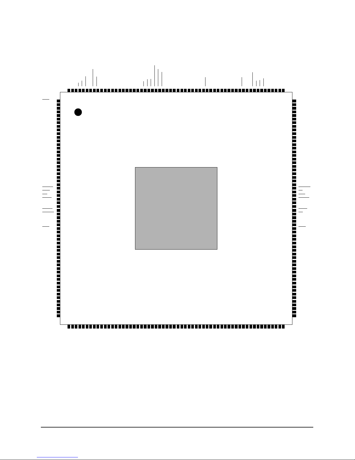
1.4 Pinout Diagram
Figure 9 contains the pin assignments for the 603.
OVDD
GND
OGNDCIWT
QACK
TBEN
TLBISYNC
RSRV
AP0
AP1
OVDD
OGND
AP2
AP3
CSE
TC0
TC1
OVDD
CLK_OUT
OGNDBRAPE
DPE
CKSTP_OUT
CKSTP_IN
HRESET
PLL_CFG0
SYSCLK
PLL_CFG1
PLL_CFG2
AVDD
PLL_CFG3
VDD
GND
LSSD_MODE
L1_TSTCLK
L2 _TSTCLK
TRST
TCK
TMS
TDI
TDO
TSIZ0
TSIZ1
TSIZ2
OVDD
OGND
TBST
TT0
TT1
SRESET
INT
SMI
MCP
TT2
TT3
OVDD
GND
OGND
GBL
A1
A3
VDD
A5
A7
A9
OGND
GND
OVDD
A11
A13
A15
VDD
A17
A19
A21
OGND
GND
OVDD
A23
A25
A27
VDD
DBW
DBG
BG
AACK
GND
A29
QREQ
ARTRY
OGND
VDD
OVDD
ABB
A31
DP0
GND
DP1
DP2
DP3
OGND
VDD
OVDD
DP4
DP5
DP6
GND
DP7
DL23
DL24
OGND
OVDD
DL25
DL26
DL27
DL28
VDD
OGND
240
239
238
237
236
235
234
233
232
231
230
229
228
227
226
225
224
223
222
221
220
219
218
217
1
2
3
4
1
5
6
7
8
9
10
11
12
13
14
15
16
17
18
19
20
21
22
23
24
O
25
26
27
28
29
30
31
32
33
34
35
36
37
38
39
40
41
42
43
44
45
46
47
48
49
50
51
52
53
54
55
56
57
58
59
60
616263646566676869707172737475767778798081828384858687888990919293949596979899
216
TOP VIEW
215
214
213
212
211
210
209
208
207
206
205
204
203
202
201
100
200
101
199
102
198
103
197
104
196
105
195
106
194
107
193
108
192
109
191
110
190
111
189
112
188
113
187
114
186
115
185
116
184
117
183
118
182
119
181
180
179
178
177
176
175
174
173
172
171
170
169
168
167
166
165
164
163
162
161
160
159
158
157
156
155
154
153
152
151
150
149
148
147
146
145
144
143
142
141
140
139
138
137
136
135
134
133
132
131
130
129
128
127
126
125
124
123
122
121
120
TT4
A0
A2
VDD
A4
A6
A8
OVDD
GND
OGND
A10
A12
A14
VDD
A16
A18
A20
OVDD
GND
OGND
A22
A24
A26
VDD
TRY
DR
TA
TEA
DBDIS
GND
A28
TS
XA
TS
OVDD
VDD
OGND
DBB
A30
DL0
GND
DL1
DL2
DL3
OVDD
VDD
OGND
DL4
DL5
DL6
GND
DL7
DL8
DL9
OVDD
OGND
DL10
DL11
DL12
DL13
VDD
OVDD
OVDD
DL29
DL30
DL31
GND
DH31
DH30
DH29
OGND
OVDD
DH28
DH27
DH26
DH25
Figure 9. PowerPC 603 Microprocessor Pin Assignments
14 603 Hardware Specifications, REV 2
Preliminary—Subject to Change without Notice
DH24
DH23
OGND
DH22
OVDD
DH21
DH20
DH19
DH18
DH17
DH16
OGND
DH15
OVDD
DH14
DH13
DH12
DH11
DH10
DH9
OGND
OVDD
DH8
DH7
DH6
DL22
DL21
DL20
OGND
OVDD
DL19
DL18
DL17
DH5
DH4
DH3
OGND
OVDD
DH2
DH1
DH0
GND
DL16
DL15
DL14
OGND
Page 15

1.5 Pinout Listing
Table 9 provides the pinout listing for the 603.
Table 9. PowerPC 603 Microprocessor Pinout Listing
Signal Name Pin Number Active I/O
A0–A31 179, 2, 178, 3, 176, 5, 175, 6, 174, 7, 170,
11, 169, 12, 168, 13, 166, 15, 165, 16, 164,
17, 160, 21, 159, 22, 158, 23, 151, 30, 144,
37
AA
CK 28 Low Input
ABB
AP0–AP3 231, 230, 227, 226 High I/O
APE
AR
TRY 32 Low I/O
AVDD 209 High Input
BG
BR
CI
CLK_OUT 221 — Output
CKSTP_IN
CKSTP_OUT
CSE 225 High Output
36 Low I/O
218 Low Output
27 Low Input
219 Low Output
237 Low Output
215 Low Input
216 Low Output
High I/O
DBB
DBDIS
DBG
DBW
O 25 Low Input
DH0–DH31 115, 114, 113, 110, 109, 108, 99, 98, 97, 94,
DL0–DL31 143, 141, 140, 139, 135, 134, 133, 131, 130,
DP0–DP7 38, 40, 41, 42, 46, 47, 48, 50 High I/O
DPE
DR
TRY 156 Low Input
GBL
GND 9, 19, 29, 39, 49, 65, 116, 132, 142, 152,
145 Low I/O
153 Low Input
26 Low Input
High I/O
93, 92, 91, 90, 89, 87, 85, 84, 83, 82, 81, 80,
78, 76, 75, 74, 73, 72, 71, 68, 67, 66
High I/O
129, 126, 125, 124, 123, 119, 118, 117, 107,
106, 105, 102, 101, 100, 51, 52, 55, 56, 57,
58, 62, 63, 64
217 Low Output
1 Low I/O
Low Input
162, 172, 182, 206, 239
603 Hardware Specifications, REV 2 15
Preliminary—Subject to Change without Notice
Page 16

Table 9. PowerPC 603 Microprocessor Pinout Listing (Continued)
Signal Name Pin Number Active I/O
HRESET 214 Low Input
INT
LSSD_MODE
L1_TSTCLK
L2_TSTCLK
1
1
1
MCP
OGND 8, 18, 33, 43, 53, 60, 69, 77, 86, 95, 103,
188 Low Input
205 Low Input
204 — Input
203 — Input
186 Low Input
Low Input
111, 120, 127, 136, 146, 161, 171, 181, 193,
220, 228, 238
OVDD 10, 20, 35, 45, 54, 61, 70, 79, 88, 96, 104,
High Input
112, 121, 128, 138, 148, 163, 173, 183, 194,
222, 229, 240
PLL_CFG0–PLL_CFG3 213, 211, 210, 208 High Input
CK 235 Low Input
QA
QREQ
RSR
V 232 Low Output
SMI
SRESET
31 Low Output
187 Low Input
189 Low Input
SYSCLK 212 — Input
T
A 155 Low Input
TBEN 234 High Input
TBST
192 Low I/O
TC0–TC1 224, 223 High Output
TCK 201 — Input
TDI 199 High Input
TDO 198 High Output
TEA
TLBISYNC
154 Low Input
233 Low Input
TMS 200 High Input
TRST
202 Low Input
TSIZ0–TSIZ2 197, 196, 195 High I/O
16 603 Hardware Specifications, REV 2
Preliminary—Subject to Change without Notice
Page 17

Table 9. PowerPC 603 Microprocessor Pinout Listing (Continued)
Signal Name Pin Number Active I/O
TS 149 Low I/O
TT0–TT4 191, 190, 185, 184, 180 High I/O
VDD 4, 14, 24, 34, 44, 59, 122, 137, 147, 157,
167, 177, 207
WT
XA
TS 150 Low I/O
Notes:
1. These are test signals for factory use only and must be pulled up to VDD for normal machine operation.
2. OVDD inputs supply power to the I/O drivers and VDD inputs supply power to the processor core. Future
members of the 603 family may use different OVDD and VDD input levels; for example, OVDD = 3.3 V or
5.0 V, with VDD = 2.5 V.
236 Low Output
High Input
1.6 Package Description
The following sections provide the package parameters and the mechanical dimensions for the 603. Note
that the 603 is currently offered in two types of CQFP packages—the Motorola wire-bond CQFP and the
IBM C4-CQFP.
1.6.1 Motorola Wire-Bond CQFP Package Description
The following sections provide the package parameters and mechanical dimensions for the Motorola
wire-bond CQFP package.
1.6.1.1 Package Parameters
The package parameters are as provided in the following list. The package type is 32 mm x 32 mm, 240-pin
ceramic quad flat pack.
Package outline 32 mm x 32 mm
Interconnects 240
Pitch 0.5 mm
603 Hardware Specifications, REV 2 17
Preliminary—Subject to Change without Notice
Page 18

1.6.1.2 Mechanical Dimensions of the Motorola Wire-Bond CQFP Package
Figure 10 shows the mechanical dimensions for the wire-bond CQFP package.
AB
θI
R
F
Pin 240
Pin 1
A
B
*Reduced pin count shown for clarity. 60 pins per side
–H–
θ2
R
G
AA
C
J
H
Min. Max.
A 30.86 31.75
B 34.6 BSC
C 3.75 4.15
D 0.5 BSC
E 0.18 0.30
F 3.10 3.90
G 0.13 0.175
H 0.45 0.55
J 0.25 –
AA 1.80 REF
AB 0.95 REF
θ12°6°
θ21°7°
R 0.15 REF
Notes: 1. BSC—Between Standard Centers.
2. All measurements in mm.
DE
*Not to scale
Figure 10. Mechanical Dimensions of the Motorola Wire-Bond CQFP Package
18 603 Hardware Specifications, REV 2
Preliminary—Subject to Change without Notice
Die Wire Bonds Ceramic Body
Alloy 42 Leads
Page 19

1.6.2 IBM C4-CQFP Package Description
The following sections provide the package parameters and mechanical dimensions for the IBM C4-CQFP
package.
1.6.2.1 Package Parameters
The package parameters are as provided in the following list. The package type is 32 mm x 32 mm, 240-pin
ceramic quad flat pack.
Package outline 32 mm x 32 mm
Interconnects 240
Pitch 0.5 mm
Lead plating Ni Au
Solder joint Sn/PB (10/90)
Lead encapsulation Epoxy
Solder-bump encapsulation Epoxy
Maximum module height 3.1 mm
Co-planarity specification 0.08 mm
Note: No solvent can be used with the C4-CQFP package. See Appendix A, “General Handling
Recommendations for the IBM Package,” for details.
603 Hardware Specifications, REV 2 19
Preliminary—Subject to Change without Notice
Page 20

1.6.2.2 Mechanical Dimensions of the IBM C4-CQFP Package
Figure 11 shows the mechanical dimensions for the C4-CQFP package.
Epoxy Dam
Clip Leadframe
Cmax
-
Solder-Bump Encapsulant
Chip
Urethane
Tape Cast Ceramic
A
0.13 TO TAL
*Reduced pin count shown for clarity. 60 pins per side
s
A-B
F
Rad
Ang
G
Jmin
H
0.08
Pin 240
Pin 1
E
A 31.8 32.2
B 34.4 34.8
-B-
C 3.05 3.15
D 0.45 0.55
E 0.18 0.28
D
0.08 TO TAL
M
-A-
B
0.13 TO TAL
s
A-B
Figure 11. Mechanical Dimensions of the IBM C4-CQFP Package
Min. Max.
A-B
* Not to scale
All measurements in mm
20 603 Hardware Specifications, REV 2
Preliminary—Subject to Change without Notice
Page 21

1.7 System Design Information
This section provides electrical and thermal design recommendations for successful application of the 603.
1.7.1 PLL Configuration
A 603 part number corresponds to a particular combination of internal (CPU core) and SYSCLK (external
bus) frequency ranges which the device has been tested to. The PLL is configured by the
PLL_CFG0–PLL_CFG3 pins. For a given SYSCLK (bus) frequency, the PLL configuration pins set the
internal CPU frequency of operation.
Table 10. PLL Configuration
Bus, CPU, and PLL Frequencies
PLL_CFG
0–3
00 00 1:1 — — — — — — 66.6
0001 1:1 — — — 33.3
0010 1:1 16.6
0100 2:1 — — — 66.6
0101 2:1 33.3
1000 3:1 — — 75
1001 3:1 50
1100 4:1 66.6
1101 4:1 — — — — — — —
CPU/
SYSCLK
Ratio
Bus
16.6 MHz
(133)
(133)
(200)
(133)
Bus
20 MHz
20
(160)
40
(160)
—— — — — —
80
(160)
Bus
25 MHz
25
(200)
50
(200)
(150)
100
(200)
Bus
33.3 MHz
(133)
—— — —
(133)
—— — —
100
(200)
—— — —
Bus
40 MHz
40
(160)
80
(160)
—— —
Bus
50 MHz
50
(200)
100
(200)
66.6 MHz
Bus
(133)
—
—
0011 PLL bypass
1111 Clock off
Notes: 1. Some PLL configurations may select bus, CPU, or PLL frequencies which are not useful, not
supported, or not tested for by the 603. PLL frequencies (sho wn in parenthesis in Table 10) should
not fall below 133 MHz, and should not exceed 200 MHz.
2. In PLL bypass mode, the SYSCLK input signal clocks the internal processor directly, the PLL is
disabled, and the bus mode is set for 1:1 mode operation. This mode is intended for factory use
only. Note that the AC timing specifications given in this document do not apply in PLL bypass
mode.
3. In clock-off mode, no clocking occurs inside the 603 regardless of the SYSCLK input.
4. PLL_CFG0–PLL_CFG1 signals select the CPU-to-bus ratio (1:1, 2:1, 3:1, 4:1),
PLL_CFG2–PLL_CFG3 signals select the CPU-to-PLL multiplier (x2, x4, x8).
603 Hardware Specifications, REV 2 21
Preliminary—Subject to Change without Notice
Page 22

1.7.2 PLL Power Supply Filtering
The AVdd power signal is pro vided on the 603 to provide po wer to the clock generation phase-lock loop. To
ensure stability of the internal clock, the power supplied to the AVdd input signal should be filtered using a
circuit similar to the one shown in Figure 12. The circuit should be placed as close as possible to the AVdd
pin to ensure it filters out as much noise as possible.
10 Ohms
Vdd AVdd
10 uF 0
GND
Figure 12. PLL Power Supply Filter Circuit
.1 uF
1.7.3 Decoupling Recommendations
Due to the 603’s dynamic power management feature, large address and data buses, and high operating
frequencies, the 603 can generate transient power surges and high frequency noise in its power supply,
especially while driving large capacitive loads. This noise must be prevented from reaching other
components in the 603 system, and the 603 itself requires a clean, tightly regulated source of power.
Therefore, it is recommended that the system designer place a decoupling capacitor with a low ESR
(effective series resistance) rating at each Vdd and OVdd pin of the 603.
These capacitors should range in value from 220 pF to 10 µF to provide both high and low frequency
filtering, and should be placed as close as possible to their associated Vdd pin. Surface-mount tantulum or
ceramic devices are preferred. It is also recommended that these decoupling capacitors receive their power
from Vdd and GND power planes in the PCB, utilizing short traces to minimize inductance in the traces.
Power and ground connections must be made to all external Vdd and GND pins of the 603.
1.7.4 Connection Recommendations
To ensure reliable operation, it is highly recommended to connect unused inputs to an appropriate signal
level. Unused acti ve-low inputs should be connected to Vdd. Unused acti ve-high inputs should be connected
to GND.
1.7.5 Thermal Management Information for the Motorola Package
This section provides a thermal management example for the 603; this example is based on a typical desktop
configuration using a 240 lead, 32 mm x 32 mm, Motorola wire-bond CQFP package. The heat sink used
for this data is a pinfin configuration from Thermalloy, part number 2338.
1.7.5.1 Thermal Characteristics for the Motorola Wire-Bond CQFP Package
The thermal characteristics for a wire-bond CQFP package are as follows:
Thermal resistance (junction-to-case) = R
1.7.5.2 Thermal Management Example
The following example is based on a typical desktop configuration using a Motorola wire-bond CQFP
package. The heat sink used for this data is a pinfin heat sink #2338 attached to the wire-bond CQFP
package with thermal grease.
θjc
or θ
= 2.2 °C/Watt (junction-to-case)
jc
22 603 Hardware Specifications, REV 2
Preliminary—Subject to Change without Notice
Page 23

Figure 13 provides a thermal management example for the Motorola wire-bond CQFP package.
35
30
25
20
15
10
Resistance (°C/watt)
Junction-to-Ambient Thermal
5
0
0123 5
Forced Convection (m/sec)
Figure 13. Motorola Wire-Bond CQFP Thermal Management Example
Motorola Wire-Bond CQFP
With Heat Sink
4
The junction temperature can be calculated from the junction-to-ambient thermal resistance, as follows:
Junction temperature: T
= Ta + R
j
θja
* P
or
= Ta + (R
T
j
+ Rcs + Rsa) * P
θjc
Where:
Ta is the ambient temperature in the vicinity of the device
is the junction-to-ambient thermal resistance
R
θja
is the junction-to-case thermal resistance of the device
R
θjc
is the case-to-heat sink thermal resistance of the interface material
R
cs
is the heat sink-to-ambient thermal resistance
R
sa
P is the power dissipated by the device
In this environment, it can be assumed that all the heat is dissipated to the ambient through the heat sink, so
the junction-to-ambient thermal resistance is the sum of the resistances from the junction to the case, from
the case to the heat sink, and from the heat sink to the ambient.
Note that verification of external thermal resistance and case temperature should be performed for each
application. Thermal resistance can vary considerably due to many factors including degree of air
turbulence.
For a power dissipation of 2.5 Watts in an ambient temperature of 40
measured above, the junction temperature of the device would be as follows:
T
= Ta + R
j
= 40 °C + (10 °C/Watt * 2.5 Watts) = 65 °C
T
j
θja
* P
which is well within the reliability limits of the device.
603 Hardware Specifications, REV 2 23
Preliminary—Subject to Change without Notice
°C at 1 m/sec with the heat sink
Page 24

Notes: 1. Junction-to-ambient thermal resistance is based on measurements on single-sided printed circuit
boards per SEMI (Semiconductor Equipment and Materials International) G38-87 in natural
convection.
2. Junction-to-case thermal resistance is based on measurements using a cold plate per
SEMI G30-88 with the exception that the cold plate temperature is used for the case temperature.
The vendors who supply heat sinks are Aavid Engineering, IERC, Thermalloy, and Wakefield Engineering.
Any of these vendors can supply heat sinks with sufficient thermal performance.
1.7.6 Thermal Management Information for the IBM Package
This section provides a thermal management example for the 603; this example is based on a typical desktop
configuration using a 240-lead, 32 mm x 32 mm, IBM C4-CQFP package. The heat sink used for this data
is a pinfin configuration from Thermalloy, part number 2338, and a flat aluminum plate with dimensions of
24 mm x 24 mm and 1.5 mm thickness.
1.7.6.1 Thermal Characteristics for the IBM C4-CQFP Package
The thermal characteristics for a C4-CQFP package are as follows:
Thermal resistance (junction to heat sink) = R
θjs
or θ
= 1.1°C/Watt (junction to heat sink)
js
1.7.6.2 Thermal Management Example
The following example is based on a typical desktop configuration using an IBM C4-CQFP package. The
heat sink used for this data is a pinfin heat sink #2338 attached to the C4-CQFP package with 2-stage epoxy .
The junction temperature can be calculated from the junction to ambient thermal resistance, as follows:
Junction temperature = T
Where:
is the ambient temperature in the vicinity of the device
T
a
is the junction-to-ambient thermal resistance
R
θja
is the junction-to-heat sink thermal resistance
R
θjs
is the heat sink-to-ambient thermal resistance
R
sa
P is the power dissipated by the device
Note: R
includes the resistance of a typical layer of thermal compound. If a lower conductivity material
θjs
is used, its thermal resistance must be included.
In this environment, it can be assumed that all the heat is dissipated to the ambient through the heat sink, so
the junction-to-ambient thermal resistance is the sum of the resistances from the junction to the heat sink
and from the heat sink to the ambient.
= Ta + R
j
= Ta + (R
T
j
or
* P
θja
+ Rsa) * P
θjs
Note that verification of external thermal resistance and case temperature should be performed for each
application. Thermal resistance can vary considerably due to many factors including degree of air
turbulence.
24 603 Hardware Specifications, REV 2
Preliminary—Subject to Change without Notice
Page 25

Figure 14 provides a thermal management example for the IBM C4-CQFP package.
40
35
30
IBM C4-CQFP
Exposed Die
25
20
Aluminum
Plate
15
10
Junction-to-Ambient
5
Thermal Resistance (°C/W)
0
Pinfin
0 0.25 0.5 1 2
Forced Convection (m/sec)
Figure 14. IBM C4-CQFP Thermal Management Example
For a power dissipation of 2.5 Watts in an ambient temperature of 40 °C at 1 m/sec with the pinfin heat sink
measured above, the junction temperature of the device would be as follows:
= Ta + R
T
j
= 40 °C + (9.1 °C/Watt * 2.5 Watts) = 63 °C
T
j
θja
* P
which is well within the reliability limits of the device.
Notes: 1. Junction-to-ambient thermal resistance is based on modeling.
2. Junction-to-heat sink thermal resistance is based on measurements and model using thermal test
chip and thermal couple which is placed on the base of the heat sink.
θ
is not measured for 0.25 m/sec convection for the pinfin.
3.
ja
The vendors who supply heat sinks are Aa vid Engineering, Thermallo y, and Wak efield Engineering. Any of
these vendors can supply heat sinks with sufficient thermal performance.
603 Hardware Specifications, REV 2 25
Preliminary—Subject to Change without Notice
Page 26

1.8 Ordering Information
This section provides the ordering information for the 603. Note that the individual part numbers correspond
to a specific combination of 603 internal/bus frequencies, which must be observed to ensure proper
operation of the device. For other frequency combinations, temperature ranges, power-supply tolerances
package types, etc., contact your local Motorola or IBM sales office.
Table 11. Ordering Information for the PowerPC 603 Microprocessor
Package T ype
Internal
Motorola IBM Motorola IBM
Wire-bond
CQFP
C4-CQFP 80 MHz 40 MHz 0100 MPC603AFE80CX PPC603-FX-080-2
Frequency
66.67 MHz 33.33 MHz 0100 MPC603AFE66CX PPC603-FX-066-2
Bus
Frequency
66.67 MHz 0000 MPC603AFE66AX PPC603-FX-066-1
Required
PLL_CFG
[0–3]
Setting
Part Numbers
1.8.1 Motorola Part Number Key
Figure 15 provides a detailed description of the Motorola part number for the 603.
MPC 603 A FE XX X X
Revision Level
Product Code
Part Identifier
Part Modifier
(A = Alpha—Original Design)
(Contact a Local Motorola Sales Office)
Bus Divider
(A = 1:1 Processor to Bus,
C = 2:1 Processor to Bus)
Processor Speed
Package
(FE = Wire-Bond CQFP)
Figure 15. Motorola Part Number Key
1.8.2 IBM Part Number Key
Figure 16 provides a detailed description of the IBM part number for the 603.
PPC 603 – F X– 0XX– X
Product Code
(1 = Internal Speed,
Part Identifier
Package
(F = C4-CQFP)
Revision Level
(Contact a Local IBM Sales Office)
Figure 16. IBM Part Number Key
26 603 Hardware Specifications, REV 2
Preliminary—Subject to Change without Notice
Internal Speed
Bus Speed
2 = Half Internal)
Page 27

Appendix A
General Handling Recommendations for the
IBM Package
The following list provides a few guidelines for package handling:
• Handle the electrostatic discharge sensitive (ESD) package with care before, during, and after
processing.
• Do not apply any load to exceed 3 Kg after assembly.
• Components should not be hot dip tinned
• The package encapsulation is an acrylated urethane. Use adequate ventilation (local exhaust) for all
elevated temperature processes.
The package parameters are as follows:
Heat sink adhesive AIEG-7655
IBM reference drawing 99F4869
Test socket Yamaichi QFP-PO 0.5-240P
Signal 165
Power/ground 75
Total 240
A.1 Package Environmental, Operation, Shipment,
and Storage Requirements
The environmental, operation, shipment, and storage requirements are as follows:
• Make sure that the package is suitable for continuous operation under business office en vironments.
— Operating environment: 10 °C to 40 °C, 8% to 80% relative humidity
— Storage environment: 1 °C to 60 °C, to 80% relative humidity
— Shipping environment: 40 °C to 60 °C, 5% to 100% relative humidity
• This component is qualified to meet JEDEC moisture Class 2 of bag
— After expiration of shelf life, packages may be baked at 120 °C (+10/–5 °C) for 4 hours
minimum and packaged. Shelf life is as specified above.
603 Hardware Specifications, REV 2 27
Preliminary—Subject to Change without Notice
Page 28

A.2 Card Assembly Recommendations
This section provides recommendations for card assembly process. Follow these guidelines for card
assembly.
• This component is supported for aqueous, IR, convection reflow, and vapor phase card assembly
processes.
• The temperature of packages should not exceed 220 °C for longer than 5 minutes.
• The package entering a cleaning cycle must not be exposed to temperature greater than that
occurring during solder reflow or hot air exposure.
• It is not recommended to re-attach a package that is removed after card assembly.
A.2.1 Card Assembly Process
During the card assembly process, no solvent can be used with the C4FP, and no more than 3 Kg of force
must be applied normal to the top of the package prior to, during, or after card assembly. Other details of
the card assembly process follow:
Solder paste Either water soluble (for example, Alpha 1208) or no clean
Solder stencil thickness 0.152 mm
Solder stencil aperature Width reduced to 0.03 mm from the board pad width
Placement tool Panasonic MPA3 or equivalent
Solder reflow Infrared, convection, or vapor phase
Solder reflow profile Infrared and/or convection
•Average ramp-up—0.48 to 1.8 °C/second
•Time above 183 °C—45 to 145 seconds
•Minimum lead temperature—200 °C
•Maximum lead temperature—240 °C
•Maximum C4FP temperature—245 °C
Vapor phase
•Preheat (board)—60 °C to 150 °C
•Time above 183 °C—60 to 145 seconds
•Minimum lead temperature—200 °C
•Maximum C4FP temperature—220 °C
•Egress temperature—below 150 °C
28 603 Hardware Specifications, REV 2
Preliminary—Subject to Change without Notice
Page 29

Clean after reflow De-ionized (D.I.) water if water-soluble paste is used
•Cleaner requirements—conveyorized, in-line
•Minimum of four washing chambers
—Pre-clean chamber: top and bottom sprays, minimum top-side
pressure of 25 psig, water temperature of 70 °C minimum, dwell
time of 24 seconds minimum, water is not re-used, water flow rate
of 30 liters/minute.
—Wash chamber #1: top and bottom sprays, minimum top-side
pressure of 48 psig, minimum bottom-side pressure of 44 psig,
water temperature of 62.5 °C (±2.5 °C), dwell time of 48 seconds
minimum, water flow rate of 350 liters/minute.
—Wash chamber #2: top and bottom sprays, minimum top-side
pressure of 32 psig, minimum bottom-side pressure of 28 psig,
water temperature of 72.5 °C (±2.5 °C), dwell time of 48 seconds
minimum, water flow rate of 325 liters/minute.
—Final rinse chamber: top and bottom sprays, minimum top-side
pressure of 25 psig, water temperature of 72.5 °C minimum, dwell
time of 24 seconds minimum, water flow rate of 30 liters/minute.
•No cleaning required if “no clean solder paste” is used
Touch-up and repair Water soluble (for example, Kester 450) or No Clean Flux
C4FP removal Hot air rework
C4FP replace Hand solder
603 Hardware Specifications, REV 2 29
Preliminary—Subject to Change without Notice
Page 30

Information in this document is provided solely to enable system and software implementers to use PowerPC microprocessors. There are no express or implied
copyright or patent licenses granted hereunder by Motorola or IBM to design, modify the design of, or fabricate circuits based on the information in this
document.
The PowerPC 603 microprocessor embodies the intellectual property of Motorola and of IBM. However, neither Motorola nor IBM assumes any responsibility or
liability as to any aspects of the performance, operation, or other attributes of the microprocessor as marketed by the other party or by any third party. Neither
Motorola nor IBM is to be considered an agent or representative of the other, and neither has assumed, created, or granted hereby any right or authority to the
other, or to any third party , to assume or create an y e xpress or implied obligations on its behalf . Information such as errata sheets and data sheets, as well as sales
terms and conditions such as prices, schedules, and support, for the product may vary as between parties selling the product. Accordingly, customers wishing to
learn more information about the products as marketed by a given party should contact that party.
Both Motorola and IBM reserve the right to modify this manual and/or any of the products as described herein without further notice. NO THING IN THIS MANU AL,
NOR IN ANY OF THE ERRA TA SHEETS, DATA SHEETS, AND OTHER SUPPORTING DOCUMENT A TION, SHALL BE INTERPRETED AS THE CONVEYANCE
BY MOTOR OLA OR IBM OF AN EXPRESS WARRANTY OF ANY KIND OR IMPLIED WARRANTY, REPRESENTATION, OR GUARANTEE REGARDING THE
MERCHANTABILITY OR FITNESS OF THE PRODUCTS FOR ANY PARTICULAR PURPOSE. Neither Motorola nor IBM assumes any liability or obligation for
damages of any kind arising out of the application or use of these materials. Any warranty or other obligations as to the products described herein shall be
undertaken solely by the marketing party to the customer, under a separate sale agreement between the marketing party and the customer. In the absence of such
an agreement, no liability is assumed by Motorola, IBM, or the marketing party for any damages, actual or otherwise.
“Typical” parameters can and do vary in different applications. All operating parameters, including “Typicals,” must be validated for each customer application by
customer’s technical experts. Neither Motorola nor IBM convey any license under their respective intellectual property rights nor the rights of others. Neither
Motorola nor IBM makes any claim, warranty , or representation, e xpress or implied, that the products described in this manual are designed, intended, or authorized
for use as components in systems intended for surgical implant into the body, or other applications intended to support or sustain life, or for any other application
in which the failure of the product could create a situation where personal injury or death may occur. Should customer purchase or use the products for any such
unintended or unauthorized application, customer shall indemnify and hold Motorola and IBM and their respective officers, employees , subsidiaries, affiliates , and
distributors harmless against all claims, costs, damages, and expenses, and reasonable attorney fees arising out of, directly or indirectly, any claim of personal
injury or death associated with such unintended or unauthorized use, even if such claim alleges that Motorola or IBM was negligent regarding the design or
manufacture of the part.
Motorola and are registered trademarks of Motorola, Inc. Motorola, Inc. is an Equal Opportunity/Affirmative Action Employer.
IBM and IBM logo are registered trademarks, and IBM Microelectronics is a trademark of International Business Machines Corp.
The PowerPC name, PowerPC logotype, PowerPC 603, and PowerPC Architecture are trademarks of International Business Machines Corp. used by Motorola
under license from International Business Machines Corp. International Business Machines Corporation is an Equal Opportunity/Affirmative Action Employer.
Motorola Literature Distribution Centers:
USA: Motorola Literature Distribution, P.O. Box 20912, Phoenix, Arizona 85036; FAX (602) 994-6430
JAPAN: Nippon Motorola Ltd., 4-32-1, Nishi-Gotanda, Shinagawa-ku, Tokyo 141 Japan.
ASIA-PACIFIC: Motorola Semiconductors H.K. Ltd., Silicon Harbour Centre, No. 2 Dai King Street, Tai Po Industrial Estate,
Tai Po, N.T., Hong Kong.
Technical Inf ormation: Motorola Inc. Semiconductor Products Sector Technical Responsiveness Center; (800) 521-6274.
Document Comments: FAX (512) 891-2638, Attn: RISC Applications Engineering.
IBM Microelectronics Division:
USA: IBM Microelectronics Division, Mail Stop A25/862-1, PowerPC Marketing, 1000 River Street, Essex Junction, VT 05452-4299;
Tel.: (800) PowerPC [(800) 769-3772]; FAX (800) POWERfax [(800) 769-3732].
EUROPE: IBM Microelectronics Division, PowerPC Marketing, Dept. 1045, 224 Boulevard J.F. Kennedy, 91105 Corbeil-Essonnes CEDEX,
France; Tel. (33) 1-60-88 5167; FAX (33) 1-60-88 4920.
JAPAN: IBM Microelectronics Division, PowerPC Marketing, Dept., R0260, 800 Ichimiyake, Yasu-cho, Yasu-gun, Shinga-ken,
Japan 520-23; Tel. (81) 775-87-4745; FAX (81) 775-87-4735.
 Loading...