

Page 1

EM78P468N/L
8-Bit Microcontroller
Product
Specification
DOC. VERSION 1.5
ELAN
MICROELECTRONICS CORP.
February 2007
Page 2

d
Trademark Acknowledgments:
IBM is a registered trademark and PS/2 is a trademark of IBM.
Windows is a trademark of Microsoft Corporation.
ELAN and ELAN logo
are trademarks of ELAN Microelectronics Corporation.
Copyright © 2004~2007 by ELAN Microelectronics Corporation
All Rights Reserved
Printed in Taiwan, ROC
The contents of in this specification are subject to change without notice. ELAN Microelectronics assumes no
responsibility concerning the accuracy, adequacy, or completeness of this specification. ELAN Microelectronics
makes no commitment to update, or to keep current the information and material contained in this specification.
Such information and material may change to conform to each confirmed order.
In no event shall ELAN Microelectronics be made responsible to any claims attributed to errors, omissions, or
other inaccuracies in the information or material contained in this specification. ELA N Microelectronics shall not
be liable for direct, indirect, specia l incidental, or consequential damages aris ing out of the use of such information
or materia l .
The software (if any) described in this specification is furnished under a license or nondisclosure agreement, and
may be used or copied only in accordance with the terms of such agreement.
ELAN Microelectronics products are not intended for use in life support appliances, devices, or systems. Use of
ELAN Microelectronics product in such applications is not supported and is prohibited.
NO PART OF THIS SPECIFICATION MAY BE REPRODUCED OR TRANSMITTED IN ANY FORM OR BY
ANY MEANS W ITHOUT THE EXPRESS WRITTEN PERMISSION OF ELAN MICROELECTRONICS.
ELAN MICROELECTRONICS CORPORATION
Headquarters:
No. 12, Innovation Road 1
Hsinchu Science Park
Hsinchu, TAIWAN 30077
Tel: +886 3 563-9977
Fax: +886 3 56 3-9966
http://www.emc.com.tw
Hong Kong:
Elan (HK) Microelectroni cs
Corporation, Ltd.
Flat A, 19F ., World Tech Centre
95 How Ming Street, Kwun Tong
Kowloon, HONG KONG
Tel: +852 2723-3376
Fax: +852 2723-7780
elanhk@emc.com.hk
Shenzhen:
Elan Microelectronics
Shenzhen, Ltd.
SSMEC Bldg., 3F, Gaoxin S. Ave.
Shenzhen Hi-Tech Industrial Park
Shenzhen, Guandong, CHINA
Tel: +86 755 2601-05 65
Fax: +86 755 2601-0500
USA:
Elan Information
Technology Group (U.S.A.)
1821 Saratoga Ave., Suite 250
Saratoga, CA 95070
U.S.A.
Tel: +1 408 366-8225
Fax: +1 408 366-8220
Shanghai:
Elan Microelectronics
Shanghai, Ltd.
23/Bldg. #115 Lane 572, Bibo Roa
Zhangjiang Hi-Tech Park
Shanghai, CHINA
Tel: +86 21 5080-3866
Fax: +86 21 5080-4600
Page 3

Contents
Contents
1 General Description······················································································ 1
2 Features········································································································· 1
3 Pin Assignment····························································································· 2
4 Block Diagram······························································································· 3
5 Pin Description······························································································ 4
6 Function Description ···················································································· 6
6.1 Operational Registers.......................................................................................... 6
6.1.1 R0/IAR (Indirect Addressing Register) ...............................................................6
6.1.2 R1/TCC (Timer Clock Counter) .......................................................................... 6
6.1.3 R2/PC (Program Counter)..................................................................................6
6.1.4 R3/SR (Status Register) .................................................................................... 8
6.1.5 R4/RSR (RAM Select Register).......................................................................... 9
6.1.6 R5/Port 5 (Port 5 I/O Data and Page of Register Select.................................... 9
6.1.7 R6/Port 6 (Port 6 I/O Data Register)................................................................... 9
6.1.8 R7/Port 7 (Port 7 I/O Data Register)................................................................... 9
6.1.9 R8/Port 8 (Port 8 I/O Data Register)................................................................. 10
6.1.10 R9/LCDCR (LCD Control Register).................................................................. 10
6.1.11 RA/LCD_ADDR (LCD Address).........................................................................11
6.1.12 RB/LCD_DB (LCD Data Buffer).........................................................................11
6.1.13 RC/CNTER (Counter Enable Register).............................................................11
6.1.14 RD/SBPCR (System, Booster and PLL Control Re gister)................................ 12
6.1.15 RE/IRCR (IR and Port 5 Setting Control Register)...........................................13
6.1.16 RF/ISR (Interrupt Status Register).................................................................... 14
6.1.17 Address: 10h~3Fh; R10~R3F (General Purpose Register)............................. 14
6.2 Special Purpose Registers ................................................................................ 15
6.2.1 A (Accumulator)................................................................................................15
6.2.2 IO C50/P5CR (Port 5 I/O and Ports 7, 8 for LCD Segment Control Register) .. 15
6.2.3 IOC60/P6CR (Port 6 I/O Control Register).......................................................16
6.2.4 IOC70/P7CR (Port 7 I/O Control Register)....................................................... 16
6.2.5 IOC80/P8CR (Port 8 I/O Control Register)....................................................... 16
6.2.6 IOC90/RAM_ADDR (128 Bytes RAM Address) ...............................................16
6.2.7 IOCA0/RAM_DB (128 Bytes RAM Data Buffer)...............................................16
6.2.8 IOCB0/CNT1PR (Counter 1 Preset Register).................................................. 17
6.2.9 IOCC0/CNT2PR (Counter 2 Preset Register)..................................................17
6.2.10 IOCD0/HPWTPR (High-Pulse Width Timer Pr eset Regis te r)................... ........ 17
6.2.11 IOCE0/LPWTPR (Low-Pulse Width Timer Preset Register) ............................18
6.2.12 IOCF0/IMR (Interrupt Mask Register)...............................................................18
6.2.13 IOC61/WUCR (Wake-up and Sink Current of P5.7/IRO UT Control Register).18
Product Specification (V1. 5) 02.15.2007 • iii
Page 4

Contents
6.2.14 IOC71/TCCCR (TCC Control Register)............................................................19
6.2.15 IOC81/WDTCR (WDT Control Register).......................................................... 20
6.2.16 IOC91/CNT12CR (Counters 1, 2 Control Register) .........................................20
6.2.17 IOCA1/HLPWTCR (High/Low Pulse Width Timer Control Register)..... ... ........ 21
6.2.18 IOCB1/P6PH (Port 6 Pull-high Control Register) .............................................22
6.2.19 IOCC1/P6OD (Port 6 Open Drain Control Register)........................................ 22
6.2.20 IOCD1/P8PH (Port 8 Pull High Control Register).............................................22
6.2.21 IOCE1/P6PL (Port 6 Pull Low Control Register).............................................22
6.3 TCC and WDT Prescaler................................................................................... 23
6.4 I/O Ports............................................................................................................. 25
6.6 Oscillator............................................................................................................ 30
6.6.1 Oscillator Modes............................................................................................... 30
6.6.2 Phase Lock Loop (PLL Mode)..........................................................................30
6.6.3 Crystal Oscillator/Ceramic Resonators (Crystal)..............................................31
6.6.4 RC Oscillator Mode with Internal Capacitor .............................. .......................32
6.7 Power-on Considerations ..................................................................................32
6.7.1 External Power-on Reset Circuit......................................................................33
6.7.2 Residue-Voltage Protection..............................................................................33
6.8 Interrupt.............................................................................................................. 34
6.9 LCD Driver .........................................................................................................35
6.9.1 R9/LCDCR (LCD Control Register).................................................................. 35
6.9.2 RA/LCD_ADDR (LCD Address)........................................................................ 36
6.9.3 RB/LCD_DB (LCD Data Buffer)........................................................................36
6.9.4 RD/SBPCR (System, Booster and PLL Control Registers).............................. 37
6.10 Infrared Remote Control Application/PWM Waveform Generate..................... 41
6.11 Code Options.....................................................................................................45
6.12 Instruction Set................................................................................................... 46
6.13 Timing Diagram................................................................................................. 49
7 Absolute Maximum Ratings······································································· 50
8 Electrical Characteristic ············································································· 51
8.1 DC Electrical Characteristics............................................................................. 51
8.2 AC Electrical Characteristics................ .. ... .. .. .. .. ... .... .. .. .. ... .. .. .. .. .. ... .. .. .... ... .. .. .. ..53
8.3 Device Characteristic.........................................................................................54
9 Application Circuit ······················································································ 66
iv • Product Specification (V1.5) 01.15.2007
Page 5

Contents
APPENDIX
A Package Type ······························································································ 67
B Package Information··················································································· 68
C EM78P468L Program Pin List····································································· 71
D ICE 468XA···································································································· 72
E Quality Assurance and Reliability······························································ 75
E.1 Address Trap Detect.......................................................................................... 75
Specification Revision History
Doc. Version Revision Description Date
1.0 Initial version 2004/04/10
1.1
1.2 1. Added LQFP Package 2005/03/15
1.3
1.4
1.5 Deleted all the packages for the EM78P468L 2007/02/15
1. Add ed DC curve vs. Temperat ure.
2. Removed the LVD function
1. Combined EM78P468N with EM78P468L Specif i cation.
2. Deleted the wake-up function from I dle mode by TCC
time out.
3. Added power-on voltage det ector in the Features secti on.
1. Modified the General Description, Features a nd Pi n
Assignment.
2. Add ed Gre en Product I nformation.
3. Modified the Functional Block Diagram.
4. Added Appendix D Quality Assurance and Reliability.
2004/12/09
2006/05/05
2007/01/11
Product Specification (V1. 5) 02.15.2007 • v
Page 6

Contents
vi • Product Specification (V1.5) 01.15. 2007
Page 7

EM78P468N/EM78P468L
8-Bit Microcontroller
1 General Description
The EM78P468N/L is an 8-bit microprocessor designed and developed with low-power and high-speed CMOS
technology. Integra ted onto a sing le chip are on chip Wa tchdog T im er ( WDT), Dat a RAM, ROM , programmable real time
clock counter, int ernal/external interrupt, power down mode, LCD driver, infrared transmitter f unction, and tri-state I/O.
The series has an on-chip 4K×13-bit Electrical One Time Programmable Read Only Memory (OTP-ROM). The
EM78P468L provides multi-protection bits to prevent intrusion of user’s OTP memory code. Seven Code option bits are
available to meet user’s requirements. Special 13 bits customer ID options are provided as well.
With its enhanced OTP-ROM feature, the EM78P468N/L provides a convenient way of developing and v erifying user’s
programs. Moreover, t his OTP device offers the advantages of easy and effective program updates, using development
and programming tools. User can avail of the ELAN Writer to easily program his development code.
2 Features
CPU Configuration
• 4K×13 bits on-chip OTP-ROM
• 144 bytes general purpose register
• 128 bytes on-chip data RAM
• 272 bytes SRAM
• 8 lev el stacks for subroutine nesting
• Power-on voltage detector provided (2.0±0.1V) for
EM78P468N
• Power-on voltage detector provided (1.7±0.1V) for
EM78P468L
I/O Port Configuration
• Typically, 12 bi-directional t ri-s tate I/O ports.
• 16 bi-directional tri-state I/O ports shared with LCD
segment output pin.
• U p to 28 bi-directional tri-state I/O ports
Operating Voltage and Temperature Range:
EM78P468N
• Commercial: 2.3V ~ 5.5 V . (at 0°C~+70°C)
• Industrial: 2.5V ~ 5.5 V. (at -40°C ~+85°C)
EM78P468L
• Commercial: 2.1 V ~ 5.5 V. (at 0°C ~+70°C)
• Industrial: 2.3V ~ 5.5 V. (at -40°C ~+85°C)
Operating Mode:
• N ormal mode: The CPU is operated on main
oscillator frequency (Fm)
• Green mode: The CPU is operated on sub-oscillator
frequency (Fs) and main oscillator (Fm) is stopped
• I dle m ode: CPU idle, LCD display remains working
• Sleep mode: The whole chip stops working
♦ Input port wake-up function (Port 6, Port 8).
Works on Idle and Sleep mode.
♦ Operation speed: DC ~ 10MHz clock input
♦ Dual clock operation
Oscillation Mode
• H igh frequency oscillator can select among Crystal,
RC, or PLL (phase loc k loop)
• Low frequency oscillator can select between Crystal
or RC mode
Peripheral Configuration
• 8-bit real time clock/counter (TCC)
• One infrared transmitter / PWM generator function
• Four sets of 8 bits auto reload down-count timer can be
used as interrupt sources
♦ Counter 1: independent down-count timer
♦ Counter 2, High Pulse Width Timer (HPW T), and
Low Pulse Width Timer (LPWT) shared with IR
function.
♦ Programmable free running on chip wat c hdog timer
(WDT). This function can operate on Normal, Green
and Idle mode.
Eight Interrupt Sources: Three External and Five Internal
• Internal interrupt source: TCC; Counters 1, 2;
High/Low pulse width timer.
• External interrupt source : INT0, INT1 and Pin change
wake-up (Port 6 and Port 8)
LCD Circuit
• Common driver pins: 4
• Segm ent driver pins: 32
• LCD Bias: 1/3, 1/2 bias
• LCD Duty: 1/4, 1/3, 1/2 duty
Package Type:
• D ice form : 59 pins
• QFP-64 pin: EM78P468NQxS/xJ
(Body 14mm × 20mm)
• LQFP-64 pin: EM78P468NAQxS/xJ
(Body 7mm × 7mm)
• LQFP-44 pin: EM78P468NBQxS/xJ
(Body 10mm × 10mm)
• QFP-44 pin: EM78P468NCQxS/xJ
(Body 10mm × 10mm)
Note: Green products do not contain hazardous
substances
Product Specification ( V 1 . 5) 02 . 1 5 . 2 007
(This specification is subject to change without further notice)
• 1
Page 8
EM78P468N/EM78P468L
8-Bit Microcontroller
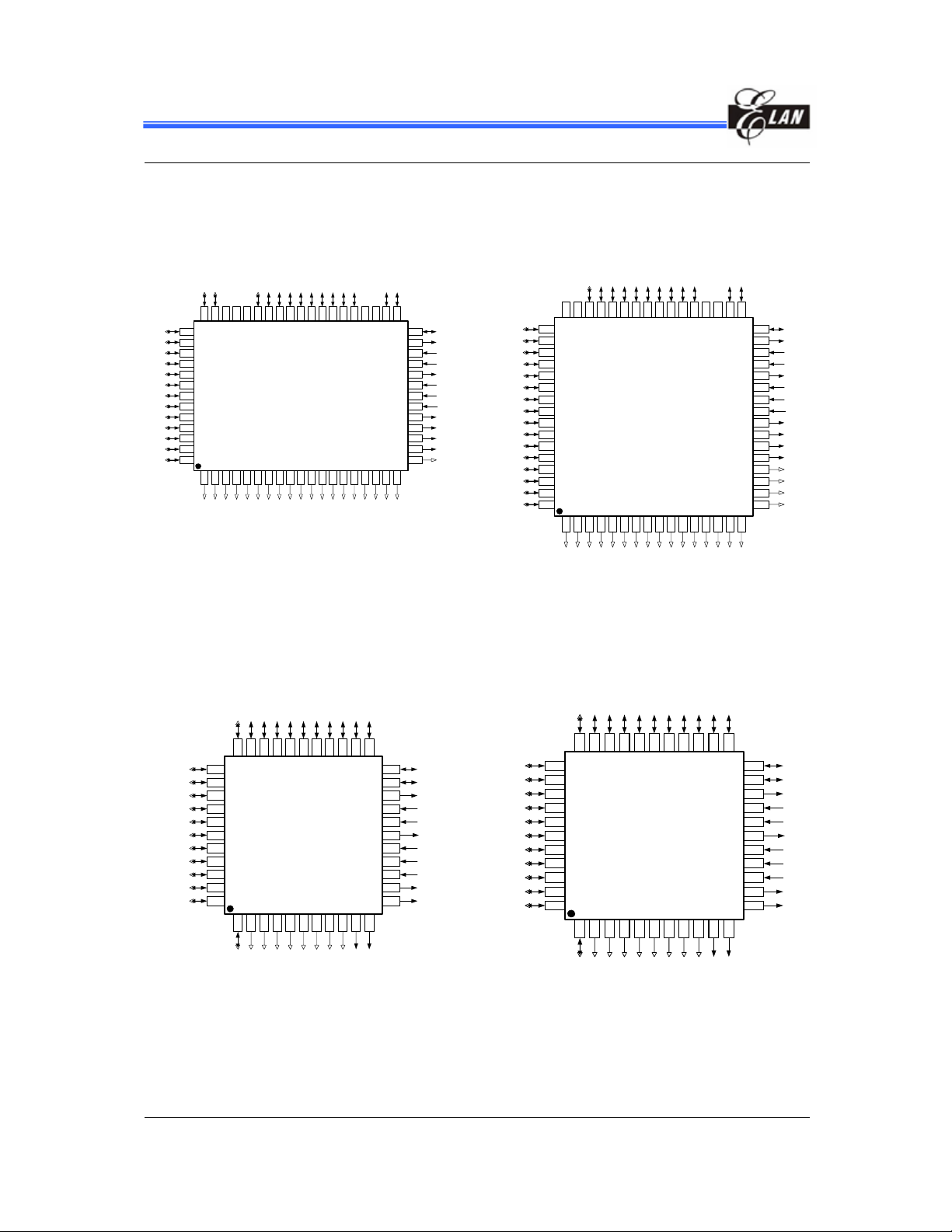
3 Pin Assignment
(1) 64-Pin QFP
SEG30/P8.6
SEG29/P8.5
1
SEG28/P8.4
SEG27/P8.3
SEG26/P8.2
SEG25/P8.1
SEG24/P8.0
SEG23/P7.7
SEG22/P7.6
SEG21/P7.5
SEG20/P7.4
SEG19/P7.3
SEG18/P7.2
SEG17/P7.1
SEG16/P7.0
52
53
54
55
56
57
58
59
60
61
62
63
64
1 2 3 4 5 6 7 8 9
SEG14
SEG15
(3) 44-Pin LQFP
P6.7
P6.6
P6.5
P6.4
NCNCNC
SEG31/P8.7
P6.3
414243444546474849505
0
EM78P468NQ
QFP-64
101
121314151617181
1
SEG 9
SEG 8
SEG 7
SEG 6
SEG13
SEG12
SEG10
SEG11
SEG 5
Fig. 3-1 64-pin QFP
(2) 64-Pin LQFP
P6.7
P6.6
P6.5
NC
P6.0
P6.1
P6.2
SEG 4
NC
NC
P5.6/TCC
P5.5/INT 1
P5.7/IROUT
333435363738394
P5.4/INT0
32
XOUT
31
XIN
30
VDD
29
OSCO
28
R-OSCI
27
GND
26
/RESET
25
VLCD3
24
VLCD2
23
VA
22
VB
21
20
COM0
9
COM3
COM2
SEG 3
SEG 2
COM1
SEG 1
SEG 0
NC 49
SEG30/P8.6 50
SEG29/P8.5
SEG28/P8.4
SEG27/P8.3
SEG26/P8.2
SEG25/P8.1
SEG24/P8.0
SEG23/P7.7
SEG22/P7.6
SEG21/P7.5
SEG20/P7.4
SEG19/P7.3
SEG18/P7.2
SEG17/P7.1
SEG16/P7.0
NC
SEG31/P8.7
8
51
52
53
54
55
56
57
58
59
60
61
62
63
64
1 2 3 4 5 6 7 8 9
SEG14
SEG13
SEG15
P6.4
EM78P468NAQ
LQFP-64
SEG 9
SEG12
SEG10
SEG11
P6.0
P6.1
P6.3
P6.2
414243444546474
0
101
SEG 8
SEG 7
SEG 6
P5.7/IROUT
121314151
1
SEG 5
SEG 4
NC
NC
P5.6/TCC
P5.5/INT1
333435363738394
P5.4/INT0
32
XOUT
31
XIN
30
VDD
29
OSCO
28
R-OSCI
27
GND
26
/RESET
25
VLCD3
24
VLCD2
23
VA
22
VB
21
20
COM0
19
COM1
18
COM2
17
COM3
6
SEG 3
SEG 2
SEG 1
SEG 0
Fig. 3-2 64-pin LQFP
(4) 44-Pin QFP
SEG27/P8.3
SEG26/P8.2
SEG25/P8.1
SEG24/P8.0
SEG23/P7.7
SEG22/P7.6
SEG21/P7.5
SEG20/P7.4
SEG19/P7.3
SEG18/P7.2
SEG17/P7.1
P6.6
P6.5
P6.4
P6.7
SEG28/P8.4
3
34
35
36
EM78P468NBQ
37
38
39
40
41
42
43
44
LQFP-44
1 2 3 4 5 6 7 8 9
SEG14
SEG13
SEG12
SEG16/P7.0
SEG11
Fig. 3-3 44-pin LQFP
P6.7
P6.6
P6.5
SEG14
SEG13
P6.4
QFP-44
SEG12
SEG11
P6.0
P6.1
P6.3
P6.2
COM3
COM2
P5.6/TCC
P5.7/IROUT
232425262728293031323
22
P5.5/INT1
21
P5.4/INT0
20
XOUT
19
XIN
18
VDD
17
OSCO
16
R-OSCI
15
GND
14
/RESET
13
VLCD3
VLCD2
12
101
1
VB
VA
COM1
COM0
SEG27/P8.3
SEG26/P8.2
SEG25/P8.1
SEG24/P8.0
SEG23/P7.7
SEG22/P7.6
SEG21/P7.5
SEG20/P7.4
SEG19/P7.3
SEG18/P7.2
SEG17/P7.1
SEG28/P8.4
3
34
35
36
EM78P468NCQ
37
38
39
40
41
42
43
44
1 2 3 4 5 6 7 8 9
SEG16/P7.0
Fig. 3-4 44-pin QFP
P6.3
COM3
P6.2
COM2
P6.1
COM1
P6.0
COM0
P5.7/IROUT
101
VB
P5.6/TCC
232425262728293031323
P5.5/INT1
22
P5.4/INT0
21
20
19
18
17
R-OSCI
16
15
/RESET
14
VLCD3
13
VLCD2
12
1
VA
2 •
Product Specification (V1.5) 02.15.2007
(This specification is subject to change without further notice)
XOUT
XIN
VDD
OSCO
GND
Page 9
Input Pin
Output Pin
Input/Output Pin
Digital I/O Pin/LCD Output Pin
LCD Output Pin
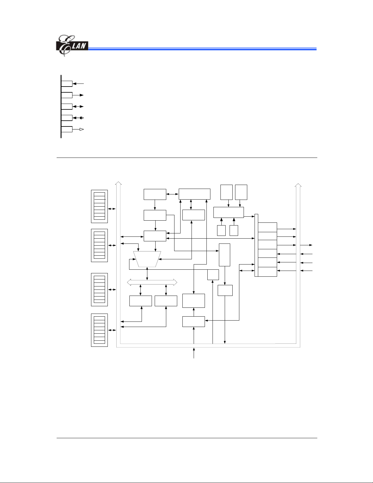
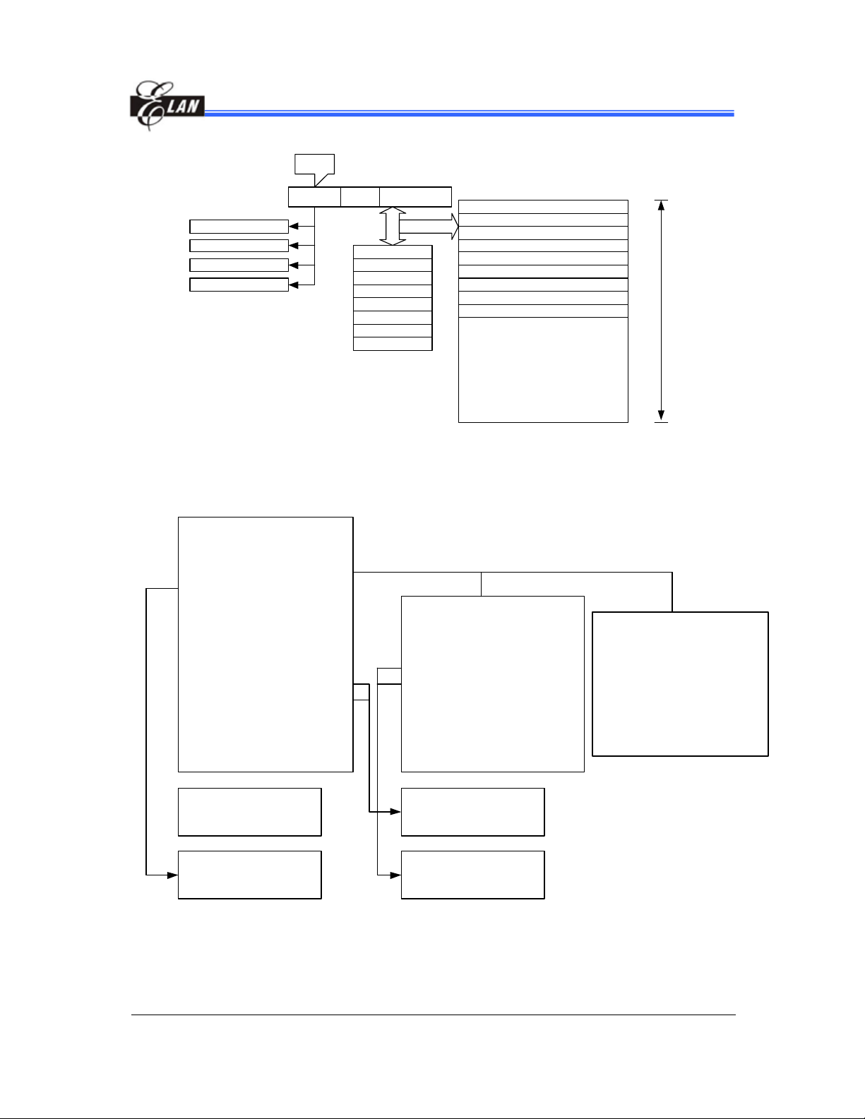
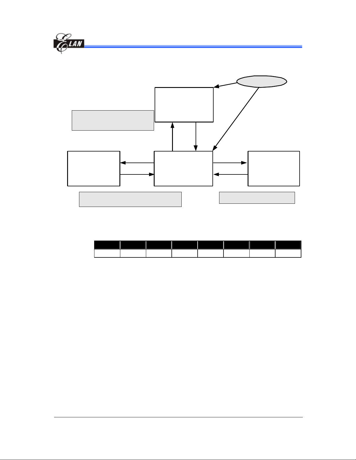
4 Block Diagram
EM78P468N/EM78P468L
8-Bit Microcontroller
P8
P80
P81
P82
P83
P84
P85
P86
P87
P7
P70
P71
P72
P73
P74
P75
P76
P77
P6
P60
P61
P62
P63
P64
P65
P66
P67
P5
P50
P51
P52
P53
P54
P55
P56
P57
ACC
ROM
Instruction
Register
Instruction
Decoder
ALU
R3 (Status
Reg.)
PC
8-level stack
(13-bit)
Interrupt
Control
Register
Interrupt
Circuit
Ext INT
Generation
PLL
R4
Oscillation
Rese
Mux.
RAM
RCCrystal
t
LCD
WDT
PWM1/IR
(Timer 1,2)
TCC
CNTR 1
CNTR 2
PWM
TCC
CNTR1
CNTR2
Fig. 4-1 System Block Diagram
Product Specification ( V 1 . 5) 02 . 1 5 . 2 007
• 3
(This specification is subject to change without further notice)
Page 10
EM78P468N/EM78P468L
8-Bit Microcontroller
5 Pin Description
Table 1 (a) Pin Description for Pa ckage of QFP64 and LQFP64
Symbol Pin No. Type Function
1-bit General purpose input/output pin/external interrupt.
P5.4/INT0 32 I/O
P5.5/INT1 33 I/O
P5.6/TCC 34 I/O
P5.7/IROUT 37 I/O
P6.0~P6.7 38~45 I/O
COM3~0 17~20 O
SEG0~SEG15 16~1 O
SEG16/P7.0
~
SEG23/P7.7
SEG24/P8.0
~
SEG30/P8.6
SEG31/P8.7
VB 21 O
VA 22 O
VLCD2 23 O
VLCD3 24 O
/RESET 25 I
R-OSCI 27 I
OSCO 28 O
Xin 30 I
Xout 31 o
NC
VDD 29 I
GND 26 I
64
~
57
56
~
50
46
35~36
47~49
O/(I/O)
O/(I/O)
INT0 interrup t source can be set to f alling or rising edge b y IOC71
register Bit 7 (INT_EDGE).
Wakes up from sleep mode and idle mode whe n the pin status
changes.
1-bit General purpose input/output pin/external interrupt.
Interrupt source is a falling edge signal.
Wakes up from sleep mode and idle mode whe n the pin status
changes.
1-bit General purpose input/output pin/external counter input.
This pin works in normal/green/idle mode.
1-bit General purpose input/output pin/IR/PWM mode output pin.
This pin is capable of sinking 20mA/5V.
8-bit General purpose input/output pins.
Pull-high, pull-low and open drain function supported.
All pins can wake up from sleep and idle modes wh en th e pin
status changes
LCD common output pin.
LCD segment output pin.
LCD segment output pin.
Can be shared with general purpose I/O pin
LCD segment output pin. Can be shared with general I/O pin.
For general purpose I/O use, can wake up from sleep mode and
idle mode when the pin status changes.
For general purpose I/O use, supports pull-hig h function.
Connect capacitors for LCD bias voltage.
Connect capacitors for LCD bias voltage.
One of LCD bias voltage.
One of LCD bias voltage.
General-purpose Input only
Low active. If it remains at logic low, the device will be reset.
In Crystal mode: crystal input
In RC mode: resi stor pull high.
In PLL mode: connect 0.01μF capacitance to GND
Connect 0.01μF capacitor to GND and code option select PLL
mode when high oscillator is not use
In Crystal mode: crystal input
In RC mode: instruction clock output
In Crystal mode: Input pin for sub-oscillator. Connect to a
32.768kHz crystal.
In Crystal mode: Connect t o a 32.768kHz crystal.
In RC mode: instruction clock output
−
No connection
Power supply
System ground pin
4 •
Product Specification (V1.5) 02.15.2007
(This specification is subject to change without further notice)
Page 11
Table 2 (b) Pin Description for Pa ckage of QFP44 and LQFP44
Symbol Pin No. Type Function
1-bit General purpose input/output pin/exter nal interrupt.
P5.4/INT0 21 I/O
P5.5/INT1 22 I/O
P5.6/TCC 23 I/O
P5.7/IROUT 24 I/O
P6.0~P6.7 25~32 I/O
COM3~0 6~9 O
SEG11~SEG14 5~2 O
SEG16/P7.0
SEG17/P7.1
~
SEG23/P7.7
SEG24/P8.0
~
SEG31/P8.4
VB 10 O
VA 11 O
VLCD2 12 O
VLCD3 13 O
/RESET 14 I
R-OSCI 16 I
OSCO 17 O
Xin 19 I
Xout 20 o
VDD 18 I
GND 15 I
1
44
~
38
37
~
33
O/(I/O)
O/(I/O)
The INT0 interrupt source can be set to falling or rising edge by
IOC71 register Bit 7 (INT_EDGE).
Wakes up from sleep mode and idle mode when the pin status
changes.
1-bit General purpose input/output pin/exter nal interrupt.
The Interrupt source is a fall ing edge signal.
Wakes up from sleep mode and idle mode when the pin status
changes.
1-bit General purpose input/output pin/external counter input.
This pin works in normal/green/ i dle mode.
1-bit General purpose input/output pin/IR/PWM mode output pin
This pin is capable of sinking 20mA/5V.
8-bit General purpose input/output pins
Pull-high, pull-low and open drain function supported.
All pins can wake up from sleep and idle modes when the pin
status changes.
LCD common output pin.
LCD segment output pin.
LCD segment output pin.
Can be shared with general purpos e I/ O pin
LCD segment output pin. Can be shared with general I/O pin
For general purpose I/O use, can wake up from sleep mode and
idle mode when the pin status changes.
For general purposes I/ O us e, supports pull-high func tion.
Connect capacitors for LCD bias voltage.
Connect capacitors for LCD bias voltage.
One of LCD bias voltage.
One of LCD bias voltage.
General-purpose Input only
Low active. If it remains at logic low, the devic e will be reset.
In Crystal mode: crystal input
In RC mode: resistor pull high.
In PLL mode: connect 0.01μF capacitance to GND
Connect 0.01μF capacit or to GND and co de option select PLL
mode when high oscillator is not use
In Crystal mode: crystal input
In RC mode: instruction clock output
In Crystal mode: Input pin for sub-oscillator. Connect to a
32.768kHz crystal.
In Crystal mode: Connect to a 32.768kHz crystal.
In RC mode: instruction clock output
Power supply
System ground pin
EM78P468N/EM78P468L
8-Bit Microcontroller
Product Specification ( V 1 . 5) 02 . 1 5 . 2 007
(This specification is subject to change without further notice)
• 5
Page 12

EM78P468N/EM78P468L
8-Bit Microcontroller
6 Function Description
6.1 Operational Registers
6.1.1 R0/IAR (Indirect Addressing Register)
(Address: 00h)
R0 is not a ph ysically implemente d register. Its majo r function is to per form as an
indirect address point er . Any instr uction using R0 as a register, actua lly accesses t he
data pointed by the RAM Select Register (R4).
6.1.2 R1/TCC (Timer Clock Counter)
(Address: 01h)
The Timer Cloc k Cou nter is i ncre mented by an exte rnal sig nal ed ge ap plied to TCC, o r
by the instruction cycle clock. It is written and read by the program as any other
register.
6.1.3 R2/PC (Program Counter)
(Address: 02h)
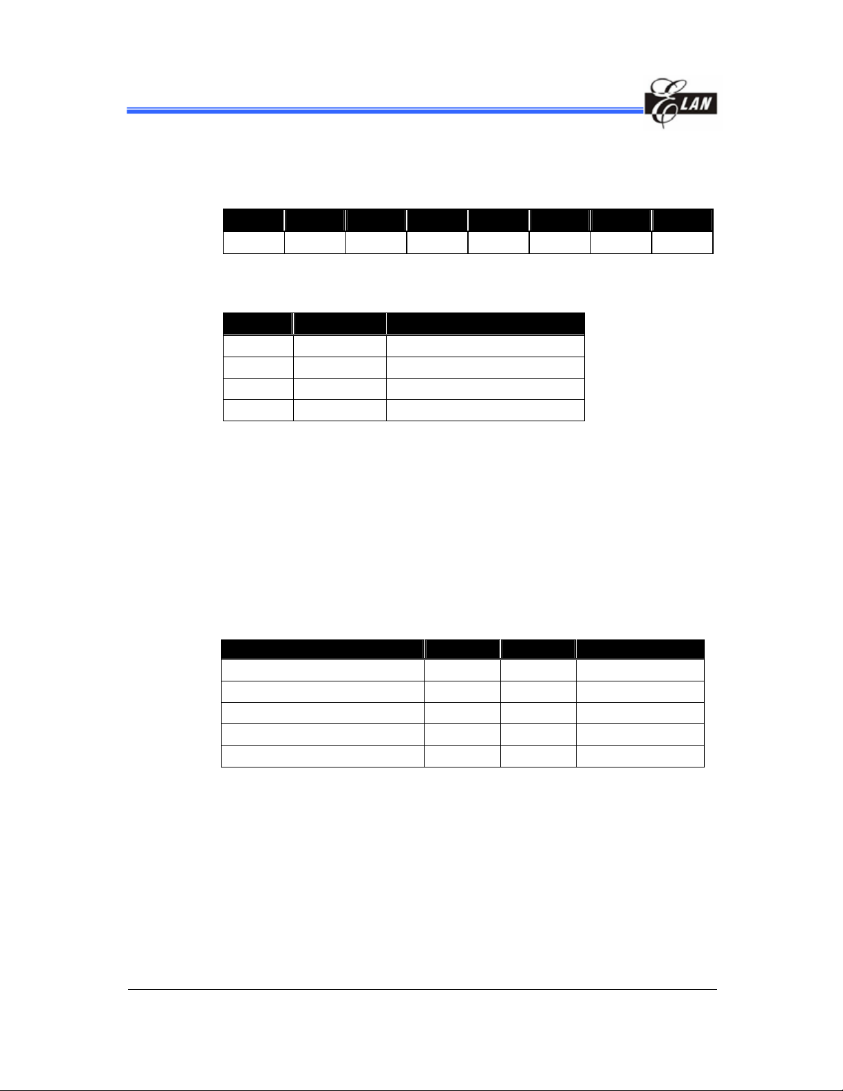
The structure of R2 is depicted in Fig. 6-1, Program Counter Organization.
The configuration structure generates 4K×13 bits on-chip ROM addresses to the
relative pr ogramming instruction codes.
The contents of R2 are all set to "0"s when a Reset condition occurs.
"JMP" inst ruct ion all ows direc t loadi ng of the l ower 10 progr am co unter bit s. Thu s,
"JMP" allows the PC to jum p to any locati on within a page.
"CALL" instruction loads the lower 10 bits of the PC, and then PC+1 is pushed onto
the stack. Thus, the subroutine entry address can be located anywhere within a
page.
"RET" ("RETL k", "RETI") instruction loads the program counter with the contents
at the top of the stack.
"ADD R2, A" allows a relative address to be added to the current PC, and the ninth
and above bits of the PC will increase progressively.
"MOV R2, A" allows loading of an address from the "A" registe r to the lower 8 bits of
the PC, and the ninth and tenth bits (A8 ~ A9) of the P C will remain unchanged.
The most significant bits (A10~A11) will be loaded with the content of PS0~PS1 in
the Status register (R3) upon execution of a "JMP" or "CALL" instruction.
6 •
Product Specification (V1.5) 02.15.2007
(This specification is subject to change without further notice)
Page 13
EM78P468N/EM78P468L
8-Bit Microcontroller
R3
A11 A10 A9 A8 A7 ~ A0
PC
00 PAGE0 0000~03FF
01 PAGE1 0400~07FF
10 PAGE2 0800~0BFF
11 PAGE3 0C00~0FFF
CALL
RET
RETL
RETI
STACK LEVEL 1
STACK LEVEL 2
STACK LEVEL 3
STACK LEVEL 4
STACK LEVEL 5
STACK LEVEL 6
STACK LEVEL 7
STACK LEVEL 8
Reset vector
TCC ov erf low interrupt v ector
Exteral INT0 pin interrupt v ector
Exteral INT1 pin interrupt v ector
Count er 1 underf low interru pt v ec t or
Count er 2 underf low interru pt v ec t or
high pulse width tim er underf lo w interrupt v ec t or
low pulse width tim er under f low inter rupt v ec t or
Port 6,Port8 pin change wake-up interrupt vector
On-Chip Program memory
000H
003H
006H
009H
00CH
00FH
012H
015H
018H
User Memory Space
ADDRESS
IAR (Indirect Addressing Register)
0 0
TCC (Time Clock Counter)
0 1
PC (Program Counter)
0 2
SR (Status Register)
0 3
RSR (RAM select register)
0 4
PORT5 (Port 5 & IOCPAGE C ontrol)
0 5
PORT6 (Port6 I/O data register)
0 6
PORT7 (Port7 I/O data register)
0 7
PORT8 (Port8 I/O data register)
0 8
LCDCR (LCD control register)
0 9
LCD_ADDR (LCD address)
0 A
LCD_DB (LCD data buffer)
0 B
CNTER (Counter enable register)
0 C
SBPCR ( System, Boos ter , PLL control )
0 D
IRCR ( IR, Pin of IR;INT 0/1;TCC c ontrol)
0 E
ISR ( i nter r upt status reg i st er )
0 F
1 0
|
16 byte c ommon r egister
1 F
Fig 6-1 Program Counter Organi zation
R5 bit 0 -> 0
control register page 0
P5CR ( Por t5 I/O & LCD seg ment contr ol )
P6CR (Port6 I/O co ntrol regis ter)
P7CR (Port7 I/O co ntrol regis ter)
P8CR (Port8 I/O co ntrol regis ter)
RAM_ADDR (128 byte RAM address)
RAM _D B ( 128 byte RAM dat a buffer)
CNT1PR (Counter 1 preset reg ister)
CNT2PR (Counter 2 preset reg ister)
HPWT PR ( H i g h-pul s e wi dth ti mer preset)
LPWTPR ( Low-puls e width ti mer pr eset)
IMR ( i nter r upt mas k reg is ter )
L CD RA M 4 * 32 b i t s
FFFH
R5 bit 0 -> 1
control register page 1
WUC R ( Wake up & P5.7 s ink cur r ent)
TCCCR (T CC & INT0 control register)
WDT CR (WDT cont rol regist er)
CN T 12CR ( Counter 1,2 control regi s ter )
HLPWT CR (hig h/ low puls e width timer contr ol )
P6PH (Port 6 pull-hig h control register)
P6OD ( Por t 6 open drai n contr ol regi s ter)
P8PH (Port 8 pull-hig h control register)
P6 PL (Port 6 pu ll-low control register)
2 0
|
3 F
bank 0 ~ bank 3
32 byte c ommon r egister
Fig. 6-2 Data Memory Conf iguration
Product Specification ( V 1 . 5) 02 . 1 5 . 2 007
(This specification is subject to change without further notice)
• 7
128 byte data RAM
Page 14
EM78P468N/EM78P468L
8-Bit Microcontroller
6.1.4 R3/SR (Status Register)
(Address: 03h)
Bit 7 Bit 6 Bit 5 Bit 4 Bit 3 Bit 2 Bit 1 Bit 0
− PS1 PS0 T P Z DC C
Bit 7: Not used
Bits 6 ~ 5 (PS1 ~ 0): Page select bits
PS1 PS0 ROM Page (Address)
0 0 Page 0 (000H ~ 3FFH)
0 1 Page 1 (400H ~ 7FFH)
1 0 Page 2 (800H ~ BFFH)
1 1 Page 3 (C00H ~ FFFH)
PS0~PS1 are used to select a ROM page. User can use the PAGE instruction ( e.g.
PAGE 1) or set PS1~PS0 bits to c hange the ROM page. W hen executing a " JMP",
"CALL", or other i nstructions wh ich causes the prog ram counter to be changed (e. g.
MOV R2, A), PS 0~PS1 are load ed int o the 11th and 1 2th bi ts of the prog ram cou nt er
where it sele cts one of the availab le progr am me mory page s. Not e that RET (R ETL,
RETI) instruction does not change the PS0~PS1 bits. That is, the return will always be
to the page from where the subroutin e was called, regardless of the current setting of
PS0~PS1 bits.
Bit 4 (T): Time-out bit. Set to 1 by the "SLEP" and "WDTC" commands or during power
up and reset to 0 by WDT timeout.
Event T P Remark
WDT wake up from sleep mode 0 0
WDT time out (not sleep mode) 0 1
/RESET wake up from sleep 1 0
Power up 1 1
Low pulse on /RESET 1 1 ×: don't care
Bit 3 (P): Power down bit. Set to 1 d uring po wer on or by a "W DTC" comm and and
reset to 0 by a "SLEP" comman d.
Bit 2 (Z): Zero flag
Bit 1 (DC): Auxiliary carry flag
Bit 0 (C): Carry flag
8 •
Product Specification (V1.5) 02.15.2007
(This specification is subject to change without further notice)
Page 15

EM78P468N/EM78P468L
8-Bit Microcontroller
6.1.5 R4/RSR (RAM Select Register)
(Address: 04h)
Bit 7 Bit 6 Bit 5 Bit 4 Bit 3 Bit 2 Bit 1 Bit 0
RBS1 RBS0 RSR5 RSR4 RSR3 RSR2 RSR1 RSR0
Bits 7 ~ 6 (RBS1 ~ RBS0): determine which ban k is activ ate d among the four banks.
See the data memory configuration in Fig. 6-2. Use the BANK instruction (e.g. BABK 1)
to change banks.
Bits 5 ~ 0 (RSR5 ~ RSR0): used to select up to 6 4 registers (Addre ss: 00~3F) in
indirect addr essing mode. If no indire ct addressing is used, the RSR can be use d as an
8-bit general purpose read/writer register.
6.1.6 R5/Port 5 (Port 5 I/O Data and Page of Register Select
(Address: 05h)
Bit 7 Bit 6 Bit 5 Bit 4 Bit 3 Bit 2 Bit 1 Bit 0
R57 R56 R55 R54 − − − IOCPAGE
Bits 7~4: 4-bits I/O registers of Port 5
User can use the IOC50 register to define e ach bit either as input or out put.
Bits 3~1: Not used
Bit 0 (IOCPAGE): change IOC5 ~ IOCF to another page
IOCPAGE = “0” : Page 0 (select register of IOC 50 to IOC F0)
IOCPAGE = “1” : Page 1 (select register of IOC 61 to IOC E1)
6.1.7 R6/Port 6 (Port 6 I/O Data Register)
(Address: 06h)
Bit 7 Bi t 6 Bit 5 Bit 4 Bit 3 Bit 2 Bit 1 Bit 0
R67 R66 R65 R64 R63 R62 R61 R60
Bits 7~0: 8-bit I/O registers of Port 6
User can use the IOC60 register to define e ach bit either as input or out put.
6.1.8 R7/Port 7 (Port 7 I/O Data Register)
(Address: 07h)
Bit 7 Bit 6 Bit 5 Bit 4 Bit 3 Bit 2 Bit 1 Bit 0
R77 R76 R75 R74 R73 R72 R71 R70
Bits 7~0: 8-bit I/O registers of Port 7
User can use the IOC70 register to define e ach bit either as input or out put.
Product Specification ( V 1 . 5) 02 . 1 5 . 2 007
(This specification is subject to change without further notice)
• 9
Page 16
EM78P468N/EM78P468L
8-Bit Microcontroller
6.1.9 R8/Port 8 (Port 8 I/O Data Register)
(Address: 08h)
Bit 7 Bit 6 Bit 5 Bit 4 Bit 3 Bit 2 Bit 1 Bit 0
R87 R86 R85 R84 R83 R82 R81 R80
Bits 7~0: 8-bit I/O registers of Port 8
User can use IOC80 register to define each bit either as input or output.
6.1.10 R9/LCDCR (LCD Control Register)
(Address: 09h)
Bit 7 Bit 6 Bit 5 Bit 4 Bit 3 Bit 2 Bit 1 Bit 0
BS DS1 DS0 LCDEN -- LCDTYPE LCDF1 LCDF0
Bit 7 (B S ) : LCD bias select bit,
BS = “0”: 1/2 bias
BS = “1”: 1/3 bias
Bit 6 ~ 5 (DS1 ~ DS0): LCD duty select
DS1 DS0 LCD Duty
0 0 1/2 duty
0 1 1/3 duty
1 × 1/4 duty
Bit 4 (LCDEN): LCD enable bit
LCDEN = “0”: LCD circuit disabled. All common/segment outputs are set to
ground (GND) level.
LCDEN = “1”: LCD circuit enabled.
Bit 3: Not used
Bit 2 (LCDTYPE): LCD drive waveform type select bit
LCDTYPE = “0” : A type waveform
LCDTYPE = “1” : B type waveform
Bits 1 ~ 0 (LCDF1 ~ LCDF0): LCD frame frequency control bits
LCDF1 LCDF0
0 0 Fs/(256×2)=64.0 Fs/(172×3)=63.5 Fs/(128×4)=64.0
0 1 Fs/(280×2)=58.5 Fs/(188×3)=58.0 Fs/(140×4)=58.5
1 0 Fs/(304×2)=53.9 Fs/(204×3)=53.5 Fs/(152×4)=53.9
1 1 Fs/(232×2)=70.6 Fs/(156×3)=70.0 Fs/(116×4)=70.6
Note: Fs: sub-oscillator frequency
10 •
Product Specific ati on (V1.5) 02.15.2007
(This specification is subject to change without further notice)
LCD Frame Frequency (e.g. Fs=32.768kHz)
1/2 Duty 1/3 Duty 1/4 Duty
Page 17

EM78P468N/EM78P468L
8-Bit Microcontroller
6.1.11 RA/LCD_ADDR (LCD Address)
(Address: 0Ah)
Bit 7 Bit 6 Bit 5 Bit 4 Bit 3 Bit 2 Bit 1 Bit 0
0 0 0 LCD_A4 LCD_A3 LCD_A2 LCD_A1 LCD_A0
Bits 7~5: Not used, fixed to “0”
Bits 4~0 (LCDA4 ~ L CDA0): LCD RAM addresses
RA
(LCD Addres s )
00H − − − − − SEG0
01H − − − − − SEG1
02H − − − − − SEG2
| | |
1DH − − − − − SEG29
1EH − − − − − SEG30
1FH − − − − − SEG31
Common × COM3 COM2 COM1 COM0
Bits 7 ~4
RB (LCD Data Buffer)
Bit 3
(LCD_D3)
(LCD_D2)
Bit 2
Bit 1
(LCD_D1)
Bit 0
(LCD_D0)
Segment
6.1.12 RB/LCD_DB (LCD Data Buffer)
(Address: 0Bh)
Bit 7 Bit 6 Bit 5 Bit 4 Bit 3 Bit 2 Bit 1 Bit 0
− − − − LCD_D3 LCD_D2 LCD_D1 LCD_D0
Bits 7~4: Not used
Bits 3~0 (LCD_D3 ~ LCD_D0) : LCD RAM data transfer register
6.1.13 RC/CNTER (Counter Enable Register)
(Address: 0Ch)
Bit 7 Bit 6 Bit 5 Bit 4 Bit 3 Bit 2 Bit 1 Bit 0
− − − − LPWTEN HPWTEN CNT2EN CNT1EN
Bits 7, 5: Not used, must be fixed to “0”
Bits 6, 4: Not used
Bit 3 (LPWTEN): low pulse width timer enable bit
LPWTEN = “0” : Disable LPWT. Stop counting operation.
LPWTEN = “1” : Enable LPWT. Start counting operation.
Bit 2 (H PWTE N): high pulse width timer enable bit
HPWTEN = “0” : Disable HPWT. Stop counting operation.
HPWTEN = “1” : Enable HPWT. Start counting operation .
Product Specification ( V 1 . 5) 02 . 1 5 . 2 007
(This specification is subject to change without further notice)
• 11
Page 18
EM78P468N/EM78P468L
8-Bit Microcontroller
Bit 1 (CNT2EN): Counter 2 enable bit
CNT2EN = “0” : Disable Counter 2. Stop counting operation.
CNT2EN = “1” : Enable Counter 2. Start counting operation.
Bit 0 (CNT1EN): Counter 1 enable bit
CNT1EN = “0” : Disable Counter 1. Stop counting operation.
CNT1EN = “1” : Enable Counter 1. Start counting operation.
6.1.14 RD/SBPCR (System, Booster and PLL Con tr ol Register )
(Address: 0Dh)
Bit 7 Bit 6 Bit 5 Bit 4 Bit 3 Bit 2 Bit 1 Bit 0
− CLK2 CLK1 CLK0 IDLE BF1 BF0 CPUS
Bit 7: Not used
Bits 6 ~ 4 (CLK2 ~ CLK0): main c lock s electi on bits f or PLL m ode (c ode opt ion selec t)
CLK2 CLK1 CLK0 Main cl ock Example Fs=32.76 8K
0 0 0 Fs×130 4.26 MHz
0 0 1 Fs×65 2.13 MHz
0 1 0 Fs×65/2 1.065 MHz
0 1 1 Fs×65/4 532 kHz
1 × × Fs×244 8 MHz
Bit 3 (IDLE): Idle mode en able bit. This bit will determine the intended mode of the
SLEP in s tructi on.
Idle = ”0”+SLEP instruction → Sleep mode
Idle = ”1”+SLEP instruction → Idle mode
* NOP instruction must be added after SLEP instruction.
Example : Idle mode : Idle bit = “1” +SLEP instruction + NOP instruction
Sleep mode : Idle bit = “0” +SLEP instruction + NOP instruction
Bits 2, 1 (BF1, 0): LCD booster frequency select bit to adjust VLCD 2, 3 driving.
BF1 BF0 Booster Frequency
0 0 Fs
0 1 Fs/4
1 0 Fs/8
1 1 Fs/16
Bit 0 (CPUS): CPU oscillator source select, When CPUS=0, the CPU oscillator select
sub-oscillator and the main oscillator is stopped.
CPUS = “0”: sub-oscillator (Fs)
CPUS = “1”: main oscillator (Fm)
12 •
Product Specific ati on (V1.5) 02.15.2007
(This specification is subject to change without further notice)
Page 19
EM78P468N/EM78P468L
8-Bit Microcontroller
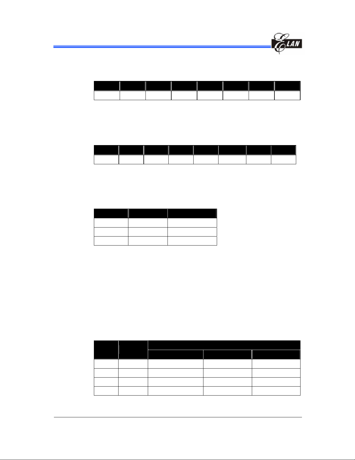
CPU Operation Mode
Code option
HLFS=1
RESET
Normal Mode
fm:oscillation
fs: oscillation
it mu s t d e l a y a l it tl e t i me s f o r th e ma i n
osc illation stable w hile your sy s tem timing
contr ol is cons c ientious
CPU : using fos c
CPUS="0"
CPUS="1"
SLEEP Mode
Fm:stop
Fs: stop
CPU: stop
The wake up time from sleep to green mode is
approx imately sub-os cillator setup time +18ms+16*1/f s
IDLE="0"
SLEP
fm:stop
fs: oscillation
CPU: using fs
Fig. 6-3 CPU Operation Mode
Green Mo de
IDLE="1"
SLEP
wa k e upWake up
The wake up time from idle to green
mode is 16*1/fs
6.1.15 RE/IRCR (IR and Port 5 Setting Control Register)
(Address: 0Eh)
Bit 7 Bit 6 Bit 5 Bit 4 Bit 3 Bit 2 Bit 1 Bit 0
IRE HF LGP − IROUTE TCCE EINT1 EINT0
Code option
HLFS=0
IDLE Mode
fm:stop
fs: oscillation
CPU: stop
Bit 7 (IRE): Infrared Remote Enable bit
IRE = “0” : Disable the IR/PWM funct ion. The state of P5.7/IROUT pin i s
determined by Bit 7 of IOC 50 if it is for IROUT.
IRE = “1” : Enable IR or PWM function.
Bit 6 (H F): High carry frequency
HF = “0” : For PWM application, disable the H/W modul ator function. The IROUT
waveform is generated according to high-pulse and low-pulse time as
determined by the respective high pulse and low pulse width timers.
Counter 2 is an independent auto reload timer.
HF = “1 ” : For IR application mode, enable the H/W modulator function, the low
time sections of the generated pulse is modulated with the Fcarrier
frequency. The Fcarrier frequency is provided by Counter 2.
Bit 5 (LGP): IROUT for of low pulse width timer
LGP = “0” : The high-pulse width timer register and low-pulse width timer is valid.
LGP = “1” : The high-pulse wi dth timer register is ignored. So the IROUT
waveform is dependent on the low-pulse width timer register only.
Product Specification ( V 1 . 5) 02 . 1 5 . 2 007
(This specification is subject to change without further notice)
• 13
Page 20

EM78P468N/EM78P468L
8-Bit Microcontroller
Bit 4: Not used
Bit 3 (IROUTE): Define the function of P5.7/IROUT pin.
IROUTE = “0” : for bi-directional general I/O pin.
IROUTE = “1” : for IR or PWM output pin , th e co ntrol bit of P5.7 (Bit 7 of IOC50)
Bit 2 (TCCE): Define the fu nction of P5.6/TCC pin.
TCCE = “0” : for bi-directional gen eral I/O pin.
TCCE = “1” : for external input pin of TCC, the control bit of P5.6 (Bit 6 of IOC50)
Bit 1 (EINT1): Define the function of P5.5/INT1 pin.
EINT1 = “0” : for bi-directional general I/O pin.
EINT1 = “1” : for extern al interrupt pin of INT1, the control bit of P5.5 (B it 5 of
Bit 0 (EINT0) : Define the function of P5.4/INT0 pin.
must be set to “0”
must be set to “1”
IOC50) must be set to “1”
EINT0 = “0” : for bi-directional general I/O pin.
EINT0 = “1” : for external interrupt pin of INT0, the control bit of P5.4 (Bit 4 of
IOC50) must be set to “1”
6.1.16 RF/ISR (Interrupt Status Register)
(Address: 0Fh)
Bit 7 Bit 6 Bit 5 Bit 4 Bit 3 Bit 2 Bit 1 Bit 0
ICIF LPWTF HPWTF CNT2F CNT1F INT1F INT0F TCIF
These bits ar e set to “1” when interrup t occurs respec tively.
Bit 7 (ICIF): Port 6, Port 8, input status changed interrupt flag. Set when Port 6, Port 8
input change s.
Bit 6 (LPWTF): interrupt flag of the internal low-pulse width timer underflow.
Bit 5 (HPWTF): interrupt flag of the int er nal high-pulse width timer underflow.
Bit 4 (CNT2F): interrupt flag of the internal Counter 2 underflo w.
Bit 3 (CNT1F): interrupt flag of the internal Counter 1 underflo w.
Bit 2 (INT1F): external INT1 pin interrupt flag.
Bit 1 (INT0F): external INT0 pin interrupt flag.
Bit 0 (TCIF): TCC timer overflow interrupt flag. Set when TCC timer overflows.
6.1.17 Address: 10h~3Fh; R10~R3F (General Purpose Register)
R10~R31F and R20~R3F (B anks 0~3) are general pur pose register s.
14 •
Product Specific ati on (V1.5) 02.15.2007
(This specification is subject to change without further notice)
Page 21

6.2 Special Purpose Registers
6.2.1 A (Accumulator)
Internal dat a transfer operation, or i nstruction operand holding usually involves the
temporary storage function of the Accum ulator, which is not an addressable register.
Registers of IOC Page 0 (IOC50 ~ IOCF0, Bit 0 of R5 = “0”)
6.2.2 IOC50/P5CR (Port 5 I/O and Ports 7, 8 for LCD Segment Control
Register)
(Address: 05h, Bit 0 of R5 = “0”)
Bit 7 Bit 6 Bit 5 Bit 4 Bit 3 Bit 2 Bit 1 Bit 0
IOC57 IOC56 IOC55 IOC54 P8HS P8LS P7HS P7LS
Bits 7~4 (IOC57~54): Port 5 I/O direction control register
IOC5x = “0”: set the relative P5.x I/O pins as output
EM78P468N/EM78P468L
8-Bit Microcontroller
IOC5x = “1”: set the relative P5.x I/O pin into high impedance (input pin)
Bit 3 (P8HS): Switch to high nibble I/O of Port 8 or to LCD segment output while
sharing
pins with SEGxx/P8.x pins.
P8HS = “0”: se lect high nibble of Port 8 as normal P8.4~P8.7
P8HS = “1”: select LCD segment output as SEG 28~SEG 31 output
Bit 2 (P8LS): Switch to low nibble I/O of Port 8 or to LCD segment output while sharing
pins with SEGxx/P8.x pins
P8LS = ”0”: select low nibble of Port 8 as normal P8.0~P8.3
P8LS = ”1”: select LCD Segment output as SEG 24~SEG 27 output
Bit 1 (P7HS): Switch to high nibble I/O of Port 7 or to LCD segment output while
sharing
pins with SEGxx/P7. x pins
P7HS = “0”: se lect high nibble of Port 7 as normal P7.4~P7.7
P7HS = “1”: select LCD Segment output as SEG 20~SEG 23 output
Bit 0 (P7LS): Switch to low nibble I/O of Port 7 or to LCD segment output while sharing
pins with SEGxx/P7.x pins
P7LS = “0”: select low nibble of Port 7 as normal P7.0~P7.3
P7LS = “1”: select LCD segment output as SEG 16~SEG 19 output
Product Specification ( V 1 . 5) 02 . 1 5 . 2 007
(This specification is subject to change without further notice)
• 15
Page 22

EM78P468N/EM78P468L
8-Bit Microcontroller
6.2.3 IOC60/P6CR (Port 6 I/O Control Register)
(Address: 06h, Bit 0 of R5 = “0”)
Bit 7 Bit 6 Bit 5 Bit 4 Bit 3 Bit 2 Bit 1 Bit 0
IOC67 IOC66 IOC65 IOC64 IOC63 IOC62 IOC61 IOC60
Bit 7 (IOC67) ~ Bit 0(IOC60): Port 6 I/O direction control register
IOC6x =”0”: set the relative Port 6.x I/O pins as output
IOC6x =”1”: set the relative Port 6.x I/O pin into high impedance (input pin)
6.2.4 IOC70/P7CR (Port 7 I/O Control Register)
(Address: 07h, Bit 0 of R5 = “0”)
Bit 7 Bit 6 Bit 5 Bit 4 Bit 3 Bit 2 Bit 1 Bit 0
IOC77 IOC76 IOC75 IOC74 IOC73 IOC72 IOC71 IOC70
Bit 7 (IOC77) ~ Bit 0 (IOC70): Port 7 I/O direction control register
IOC7x = “0”: set the relative Port 7.x I/O pins as output
IOC7x = “1”: set the relative Port 7.x I/O pin into high impedance (input pin)
6.2.5 IOC80/P8CR (Port 8 I/O Control Register)
(Address: 08h, Bit 0 of R5 = “0”)
Bit 7 Bit 6 Bit 5 Bit 4 Bit 3 Bit 2 Bit 1 Bit 0
IOC87 IOC86 IOC85 IOC84 IOC83 IOC82 IOC81 IOC80
Bit 7 (IOC 87) ~ Bit 0 (IOC 80): Port 8 I/O direction control register
IOC8x = “0”: set the relative Port 8.x I/O pins as output
IOC8x = “1”: set the relative Port 8.x I/O pin into high impedance (input pin)
6.2.6 IOC90/RAM_ADDR (128 Bytes RAM Address)
(Address: 09h, Bit 0 of R5 = “0”)
Bit 7 Bit 6 Bit 5 Bit 4 Bit 3 Bit 2 Bit 1 Bit 0
0 RAM_A6 RAM_A5 RAM_A4 RAM_A3 RAM_A2 RAM_A1 RAM_A0
Bit 7: Not used, fixed at “0”
Bits 6~0: 128 bytes RAM address
6.2.7 IOCA0/RAM_DB (128 Bytes RAM Data Buffer )
(Address: 0Ah, Bit 0 of R5 = “0”)
Bit 7 Bit 6 Bit 5 Bit 4 Bit 3 Bit 2 Bit 1 Bit 0
RAM_D7 RAM_D6 RAM_D5 RAM_D4 RAM_D3 RAM_D2 RAM_D1 RAM_D0
Bits 7~0: 128 bytes RAM data transf er r egister
16 •
Product Specific ati on (V1.5) 02.15.2007
(This specification is subject to change without further notice)
Page 23
EM78P468N/EM78P468L
8-Bit Microcontroller
6.2.8 IOCB0/CNT1PR (Counter 1 Preset Register)
(Address: 0Bh, Bit 0 of R5 = “0”)
Bit 7 Bit 6 Bit 5 Bit 4 Bit 3 Bit 2 Bit 1 Bit 0
Bit 7 Bit 6 Bit 5 Bit 4 Bit 3 Bit 2 Bit 1 Bit 0
Bit 7 ~ Bit 0: These are Counter 1 buffers which user can read and write. Counter 1 is
an 8-bit down -c ount timer with 8-b it pre s ca ler us ed to pre set th e cou nt er a nd read the
preset value. The prescaler is set by the IOC91 register. After an interrupt, it will auto
reload the preset value.
6.2.9 IOCC0/CNT2PR (Counter 2 Preset Register)
(Address: 0Ch, Bit 0 of R5 = “0”)
Bit 7 Bit 6 Bit 5 Bit 4 Bit 3 Bit 2 Bit 1 Bit 0
Bit 7 Bit 6 Bit 5 Bit 4 Bit 3 Bit 2 Bit 1 Bit 0
Bit 7 ~ Bit 0: These are Counter 2 buffers which user can read and write. Counter 2 is
an 8-bit down -c ount timer with 8-b it pre s ca ler us ed to pre set th e cou nt er a nd read the
preset value. The prescaler is set by IOC91 register. After an interrupt, it will reload the
preset value.
When IR output is enabled, this control register can obtain carrier frequency output.
If the Counter 2 clock source is equal to F
, then
T
F
Carrier frequency (Fcarrier) =
T
prescaler*)1+value_preset(*2
6.2.10 IOCD0/HPWTPR (High- P ulse Wid th Tim er P r eset Reg ist er)
(Address: 0Dh, Bit 0 of R5 = “0”)
Bit 7 Bit 6 Bit 5 Bit 4 Bit 3 Bit 2 Bit 1 Bit 0
Bit 7 Bit 6 Bit 5 Bit 4 Bit 3 Bit 2 Bit 1 Bit 0
Bit 7 ~ Bit 0: These are high-pulse width timer buffers which user can read and write.
High-pulse width timer pres et register is an eight-bit down-counter with 8-bit prescaler
used as IOCD0 to preset the counter and read the preset value. The prescaler is set by
the IOCA1 re gister. After an interrupt, it will reload the preset value.
For PWM or IR application, this control register is set as high pulse width.
If the high-pulse width timer clock source is F
High pulse time =
, then
T
)1+value_preset(*prescaler
F
T
Product Specification ( V 1 . 5) 02 . 1 5 . 2 007
(This specification is subject to change without further notice)
• 17
Page 24
EM78P468N/EM78P468L
8-Bit Microcontroller
6.2.11 IOCE0/LPWTPR (Low-Pulse Width Timer Preset Register)
(Address: 0Eh, Bi t 0 of R5 = “0”)
Bit 7 Bit 6 Bit 5 Bit 4 Bit 3 Bit 2 Bit 1 Bit 0
Bit 7 Bit 6 Bit 5 Bit 4 Bit 3 Bit 2 Bit 1 Bit 0
Bit 7 ~ Bit 0: All are low-pulse width timer buffer that user can read and write.
Low-pulse width timer preset is an eight-bit down-counter with 8-b it prescaler that is
used as IOCE0 t o preset t he counter an d read prese t value. The pr escaler is set by
IOCA1 register. After an interrupt, it will reload the preset value.
For PWM or IR application, this control register is set as low pulse wi dth.
If the low-pulse width timer clock source is F
, then
T
)1+value_preset(*prescaler
Low pulse ti me =
F
T
6.2.12 IOCF0/IMR (Interrupt Ma sk Regis ter )
(Address: 0Fh, Bit 0 of R5 = “0”)
Bit 7 Bit 6 Bit 5 Bit 4 Bit 3 Bit 2 Bit 1 Bit 0
ICIE LPWTE HPWTE CNT2E CNT1E INT1E INT0E TCIE
Bit 7 ~ Bi t 0: interrupt enable bit. Enable the respective interrupt source.
0: disable interrupt
1: enable interrupt
IOCF0 register is readable and writable.
Registers of IOC Page 1 (IOC61 ~ IOCE1, Bit 0 of R5 = “1”)
6.2.13 IOC61/WUCR (Wake-up and Sink Current of P5.7/IROUT
Control Register)
(Address: 06h, Bit 0 of R5 = “1”)
Bit 7 Bit 6 Bit 5 Bit 4 Bit 3 Bit 2 Bit 1 Bit 0
IROCS -- -- -- /WUE8H /WUE8L /WUE6H /WUE6L
Bit 7: IROCS: IROUT/Port 5.7 output sink current set
IROCS
0 10 mA 6 mA
1 20 mA 12 mA
P5.7/IROUT Sink Current
VDD=5V VDD=3V
Bits 6, 5, 4: Not used
Bit 3 (/WUE8H): 0/1→ enable/disable P8.4~P8 .7 pin change wake-up functio n
18 •
Product Specific ati on (V1.5) 02.15.2007
(This specification is subject to change without further notice)
Page 25
EM78P468N/EM78P468L
8-Bit Microcontroller
Bit 2 (/WUE8L): 0/1 → enable/disable P8.0~P8.3 pin change wake-up function
Bit 1 (/WUE6H): 0/1 → enable/disable P6.4~P6.7 pin chang e wake-up function
Bit 0 (/WUE6L): 0/1 → enable/disable P6.0~P6.3 pin change wake-up function
* Port 6 and Port 8 must not be set as input f loating when wake-up function is
enabled. “Enable” is the initial sta te of wake-up function.
6.2.14 IOC71/TCCCR (TCC Control Register)
(Address: 07h, Bit 0 of R5 = “1”)
Bit 7 Bit 6 Bit 5 Bit 4 Bit 3 Bit 2 Bi t 1 Bit 0
INT_EDGE INT TS TE PSRE TCCP2 TCCP1 TCCP0
Bit 7 (INT_EDGE):
INT_EDGE = “0”:
Interrupt on the rising edge of P5.4/INT0 pi n
INT_EDGE = “1”: Interrupt on the falling edge of P5.4/INT0 pin
Bit 6 (INT): INT enable flag, this bit is read only
INT = “0”: interr upt masked by DISI or hardware interrupt
INT = “1”: interrupt enabled by ENI/RETI instructions
Bit 5 (TS): TCC signal source
TS = “0”: internal instruction cycle clock
TS = “1”: transition on TCC pin, TCC period > internal instruction clock period
Bit 4 (TE):
TCC signal edge
TE = “0”: incremented by TCC pin rising edge
TE = “1”: incremented by TCC pin falling edge
Bits 3~0 (PSRE, TCCP2 ~ TCCP0): TCC prescaler bits.
PSRE TCCP2 TCCP1 TCCP0 TCC Rate
0 × × × 1:1
1 0 0 0 1:2
1 0 0 1 1:4
1 0 1 0 1:8
1 0 1 1 1:16
1 1 0 0 1:32
1 1 0 1 1:64
1 1 1 0 1:128
1 1 1 1 1:256
Product Specification ( V 1 . 5) 02 . 1 5 . 2 007
(This specification is subject to change without further notice)
• 19
Page 26

EM78P468N/EM78P468L
8-Bit Microcontroller
6.2.15 IOC81/WDTCR (WDT Control Register)
(Address: 08h, Bit 0 of R5 = “1”)
Bit 7 Bit 6 Bit 5 Bit 4 Bit 3 Bit 2 Bit 1 Bit 0
− − − − WDTE WDTP2 WDTP1 WDTP0
Bits 7 ~ 4: Not used
Bit 3 (WDTE): Watchdog timer enable. This cont rol bit is used to enable the Watchdog
timer,
WDTE = “0”: Disable WDT function
WDTE = “1”: enable WDT function
Bits 2 ~ 0 (WDTP2 ~ WDTP0): Watchdog Timer prescaler bits. The WDT clock source
is sub-oscillation frequency.
WDTP2 WDTP1 WDTP0 WDT Rate
0 0 0 1:1
0 0 1 1:2
0 1 0 1:4
0 1 1 1:8
1 0 0 1:16
1 0 1 1:32
1 1 0 1:64
1 1 1 1:128
6.2.16 IOC91/CNT12CR (Counters 1, 2 Control Register)
(Address: 09h, Bit 0 of R5 = “1”)
Bit 7 Bit 6 Bit 5 Bit 4 Bit 3 Bit 2 Bit 1 Bit 0
CNT2S CNT2P2 CNT2P1 CNT2P0 CNT1S CNT1P2 CNT1P1 CNT1P0
Bit 7(CNT2S): Counter 2 clock source select 0/1 → Fs/ Fm*
(*Fs: sub-oscillator clock, Fm: main-oscillator clock)
Bits 6~4 (CNT2P2 ~ CNT2P 0): Counter 2 prescaler select bits
CNT2P2 CNT2P1 CNT1P0 Counter 2 Scale
0 0 0 1:2
0 0 1 1:4
0 1 0 1:8
0 1 1 1:16
1 0 0 1:32
1 0 1 1:64
1 1 0 1:128
1 1 1 1:256
20 •
Product Specific ati on (V1.5) 02.15.2007
(This specification is subject to change without further notice)
Page 27

EM78P468N/EM78P468L
8-Bit Microcontroller
Bit 3 (CNT1S): Counter 1 clock source select 0/1 → Fs/ Fm*
Bits 2~0 (CNT1P2 ~ CNT1P20):
CNT1P2 CNT1P1 CNT1P0 Counter 1 Scale
0 0 0 1:2
0 0 1 1:4
0 1 0 1:8
0 1 1 1:16
1 0 0 1:32
1 0 1 1:64
1 1 0 1:128
1 1 1 1:256
Counter 1 prescaler select bits
6.2.17 IOCA1/HL PWTCR (High/ Low Pulse Width Timer Co ntrol Register )
(Address: 0Ah, Bit 0 of R5 = “1”)
Bit 7 Bit 6 Bit 5 Bit 4 Bit 3 Bit 2 Bit 1 Bit 0
LPWTS LPWTP2 LPWTP1 LPWTP0 HPWTS HPWTP2 HPWTP1 HPWTP0
Bit 7 (LPWTS): low-pulse width timer clock source select 0/1 → Fs/ Fm*
(*Fs: sub-oscillator clock, Fm: main-oscillator clock)
Bits 6~4 (LPWTP2~ LPWTP0): low-pulse width timer prescaler select bits
LPWTP2 LPWTP1 LPWTP0 Low-pulse Width Timer Scale
0 0 0 1:2
0 0 1 1:4
0 1 0 1:8
0 1 1 1:16
1 0 0 1:32
1 0 1 1:64
1 1 0 1:128
1 1 1 1:256
Bit 3 (HPWTS): high-pulse width timer clock source select 0/ 1 → Fs/ Fm*
Bits 2~0 (HPWTP2~ HPWTP0): high-pulse width timer prescaler select bits
HPWTP2 HPWTP1 HPWTP0 High-pulse Width Timer Scale
0 0 0 1:2
0 0 1 1:4
0 1 0 1:8
0 1 1 1:16
1 0 0 1:32
1 0 1 1:64
1 1 0 1:128
1 1 1 1:256
Product Specification ( V 1 . 5) 02 . 1 5 . 2 007
(This specification is subject to change without further notice)
• 21
Page 28

EM78P468N/EM78P468L
8-Bit Microcontroller
6.2.18 IOCB1/P6PH (Port 6 Pull-high Control Register)
(Address: 0Bh, Bit 0 of R5 = “1”)
Bit 7 Bit 6 Bit 5 Bit 4 Bit 3 Bit 2 Bit 1 Bit 0
PH67 PH66 PH65 PH64 PH63 PH62 PH61 PH60
Bit 7 ~ Bit 0 (PH67 ~ PH60): The enable bits of Port 6 pull high function.
PH6x = “0”: disable pin of P6.x internal pull-high resistor function
PH6x = “1”: en able pin of P6.x internal pull-high resistor function
6.2.1 9 IOCC1/ P6OD (P o rt 6 Op en Drain Contr ol Regi ster)
(Address: 0Ch, Bit 0 of R5 = “1”)
Bit 7 Bit 6 Bit 5 Bit 4 Bit 3 Bit 2 Bit 1 Bit 0
OP67 OP66 OP65 OP64 OP63 OP62 OP61 OP60
Bit 7 ~ Bi t 0: The enable bits of Port 6 open drain function.
OD6x = “0”: disable pin of P6.x open drain function
OD6x = “1”: enable pin of P6.x open drain function
6.2.20 IOCD1/P8PH (Port 8 Pull High Control Register)
(Address: 0Dh, Bit 0 of R5 = “1”)
Bit 7 Bit 6 Bit 5 Bit 4 Bit 3 Bit 2 Bit 1 Bit 0
PH87 PH86 PH85 PH84 PH83 PH82 PH81 PH80
Bit 7 ~ Bi t 0: The enable bits of PORT 8 pull-high function.
PH8x = “0”: disable pin of P8.x internal pull-high resistor function
PH8x = “1”: enable pin of P8.x pull-high resistor function
6.2.21 IO CE1/P 6P L (Por t 6 Pull Low Control Register)
(Address: 0Eh, Bit 0 of R5 = “1”)
Bit 7 Bit 6 Bit 5 Bit 4 Bit 3 Bit 2 Bit 1 Bit 0
PL67 PL66 PL65 PL64 PL63 PL62 PL61 PL60
Bit 7 ~ Bi t 0: The enable bits of Port 6 pull low function.
PL6x = “0”:
PL6x = “1”: enable pin of P6.x internal pull-low resistor functi on
disable pin of P6.x internal pull-low resistor function
22 •
Product Specific ati on (V1.5) 02.15.2007
(This specification is subject to change without further notice)
Page 29

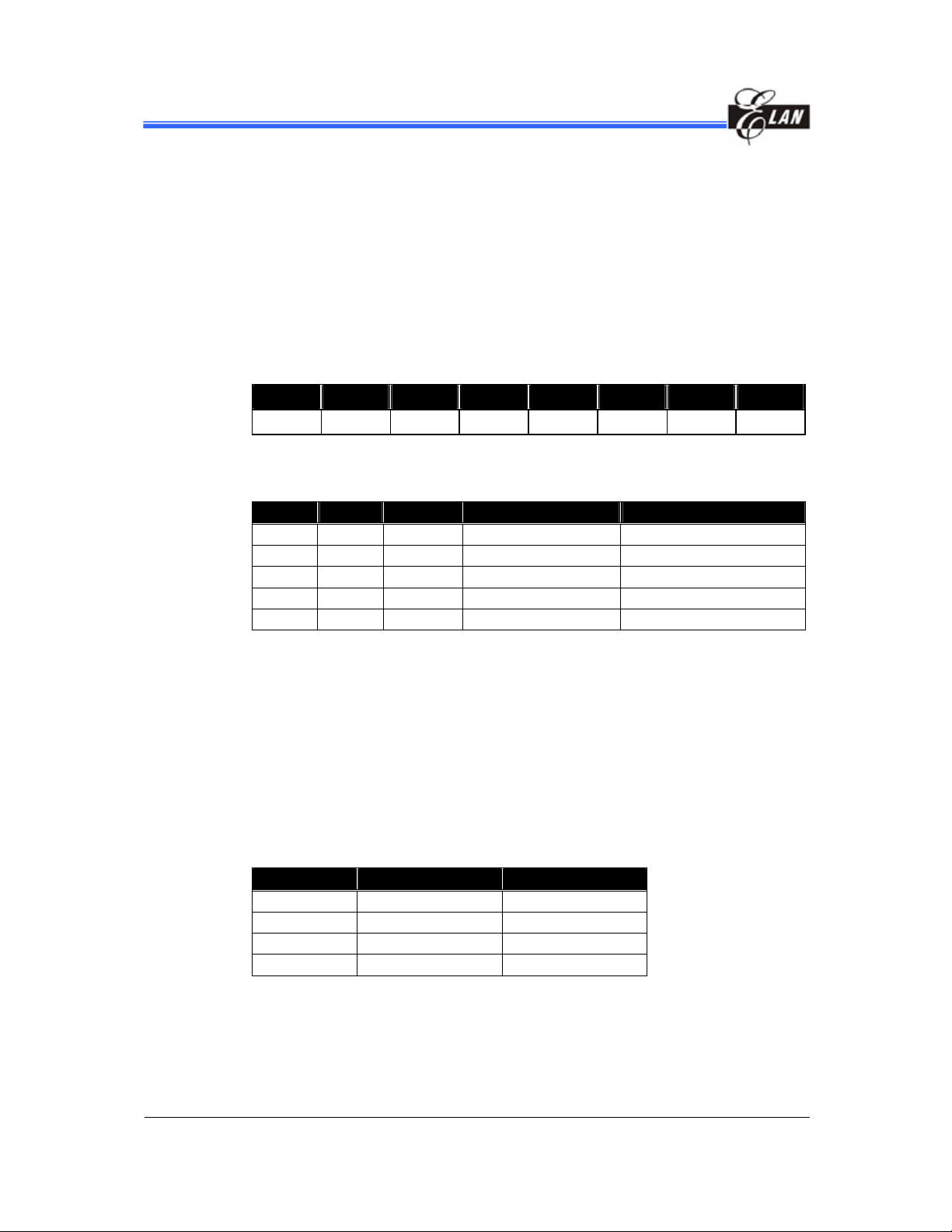
6.3 TCC and WDT Prescaler
Two 8-bit counters are available as prescalers for the TCC (Time Clock Counter) and
WDT (Wat chdog Timer) . The TCCP2~TCCP0 bit s of the IOC7 1 register are used to
determine the ratio of the TCC prescaler. Likewise, the WDTP2~WDTP0 bits of t he
IOC81 register are used to determine the WDT prescaler. The TCC prescaler
(TCCP2~TCCP0) is cleared by the instructions each time they are written into TCC,
while the WDT prescaler is cleared by the “WDTC” and “SLEP” instructions. Fig.7
depicts the circuit diagram of TCC and WDT.
R1 (TCC) is a n 8-bit timer/counter. The cloc k source of TCC can be selected by
internal instruc tion clo ck or ex terna l signal input (ed ge selec tabl e from the TCC contr ol
register). If the TCC signal source is from the internal instruction clock, the TCC will be
incremente d by 1 at every instruction cycle (without prescaler). If th e TCC signal
source is from a n extern al clock inpu t, the TCC wi ll be inc remented by 1 at eve ry falling
edge or rising edge of the TCC pin.
The Watchdog Timer is a free running on sub-oscillator. The WDT will keep on running
even after the oscillator driver has been turned off. During Normal mode, Green mode,
or Idle mode operati on, a WDT time-out (if enabled) will cause the device t o reset. The
WDT can be enabled or disabled at any time during the Normal mode and Green mode
by software programming. Refer to WDTE bit of IOC81 r egister. The WDT time-out
period is equal to (prescaler
× 256 / (Fs/2)).
EM78P468N/EM78P468L
8-Bit Microcontroller
Instruction Clock = Fosc /2
Fosc: CP U operate frequency
TCC
Pin
TE (IOC71 )
WDTE (IOC81)
MUX
TS (IOC71)
Prescaler
PSRE
(IOC71)
TCCP2~0
Fig. 6-4(a) Block Diagram of TCC
8 bit counterWDT
8 to 1 MUX
WDT Time ou t
Fig. 6-4(b) Block Diagr am of WDT
Prescaler
WDT P2~0
(IOC81)
(IOC71)
Dat a B u s
TCC (R1)
8 to 1 MUX
TC C overflow interrupt
Fs/2
(Fs:Sub osc illator)
Product Specification ( V 1 . 5) 02 . 1 5 . 2 007
(This specification is subject to change without further notice)
• 23
Page 30

EM78P468N/EM78P468L
8-Bit Microcontroller
WDT Setting Flowchart
START
Use WDT function ?
Y
N
Enable WDT function : set bit 7 of
Code option Word 0 to "0"
Setting WDT prescaler
(IOC81 register)
Enable WDT
(bit 3 of IOC81)
END
Disable WDT function : set bit 7 of
Code option Word 0 to "1"
WDTtime= prescaler*256/Fs
Fs: sub-oscillator frequency
TCC Setting Flowchart
START
from External Input
TCC clock source?
External/ instruction cycle
from Instruction Cycle
*set clock source from external TCC pin
(set bit 4 of IOC71 to "1")
*set P5.6/TCC for TCC input Pin
( set bit 2 of RE to "1" and set bit 6 of IOC 50 to "1")
*choose TCC pin operation edge
(set by bit 4 of IOC71)
*choose TCC prescaler
(set by bit 0 to bit 3 of IOC71)
* Enable TCC interrupt Mask
(set bit 0 of IOCF0 to "1")
*Clear TCC interrupt Flag
(set bit 0 of RF to "0")
Enable TCC to start count
(use ENI instruction)
END
24 •
Product Specific ati on (V1.5) 02.15.2007
*choose TCC clock source from instruction cycle
(set bit 4 of IOC71 to "0")
*choose TCC prescaler
(set by bit 0 to bit 3 of IOC71)
(This specification is subject to change without further notice)
Page 31

6.4 I/O Ports
EM78P468N/EM78P468L
8-Bit Microcontroller
The I/O registers, (Port 5, Port 6, Port 7 and Port 8), are bi-directional tri -state I/O ports .
Port 6 and Port 8 are p ulled-high internally by software; Port 6 is also pulled-low i nternally
by software. Fu rthermore, P o rt 6 has its open-drain output also through sof tware. Port 6
and Port 8 features an input status changed i nter rupt (o r wake-up) functi on and is
pulled-high by software. Each I/O pin can be defined as "input" or "output" pin by the I/O
control register (IOC50 ~ IOC80). The I/O registers and I/O control regist ers are both
readable and writable. The I/O interface circuits are shown in Fig . 6-5 .
Note: Open-drain, pull-hig h, and pull down are not shown in the figure.
Fig. 6-5 The Circuit of I/O Port and I/O Control Register for Port 5 ~ 8
6.5 Reset and Wake-up
A reset can be activated by
POR (Power-on Reset)
WDT timeout. (if enabled)
/RESET pin goes to low.
Note: The reset circuit is always enabled. It will reset the CPU at 1.9V.
Once a reset occurs, the f ollowing fun ctions are performed
The oscillat or is running, or will be started.
The program c ounter (R2/PC) is set to all "0".
All I/O port pins are configured as input mode (high-impedance state).
The TCC/Watchdog timer and prescaler are cleared.
When power is on, the Bits 5 and 6 of R3 and the upper two bits of R4 are cleared.
Bits of the IOC71 register are set to all "1" except for Bit 6 (INT flag).
For other re gisters, see Table 2.
Product Specification ( V 1 . 5) 02 . 1 5 . 2 007
(This specification is subject to change without further notice)
• 25
Page 32

EM78P468N/EM78P468L
8-Bit Microcontroller
Table 2 Summary of Regi st ers I nit ia lized Values
Address Name Reset Type Bit 7 Bit 6 Bit 5 Bit 4 Bit 3 Bit 2 Bit 1 Bit 0
Bit Name IOC57 IOC56 IOC55 IOC54 P8HS P8LS P7HS P7LS
0x05
0x06
0x07
0x08
0x09
0x0A
0x0B
0x0C
0x0D
0x0E
0x0F
0x06
IOC50
(P5CR)
IOC60
(P6CR)
IOC70
(P7CR)
IOC80
(P8CR)
IOC90
(RAM_ADDR)
IOCA0
(RAM_DB)
IOCB0
(CNT1PR)
IOCC0
(CNT2PR)
IOCD0
(HPWTPR)
IOCE0
(LPWTPR)
IOCF0
(IMR)
IOC61
(WUCR)
Power-on 1 1 1 1 0 0 0 0
/RESET & WDT 1 1 1 1 0 0 0 0
Wake-up from
Pin Change
Bit Name IOC67 IOC66 IOC65 IOC64 IOC63 IOC62 IOC61 IOC60
Power-on 1 1 1 1 1 1 1 1
/RESET & WDT 1 1 1 1 1 1 1 1
Wake-up from
Pin Change
Bit Name IOC77 IOC76 IOC75 IOC74 IOC73 IOC72 IOC71 IOC70
Power-on 1 1 1 1 1 1 1 1
/RESET & WDT 1 1 1 1 1 1 1 1
Wake-up from
Pin Change
Bit Name IOC87 IOC86 IOC85 IOC84 IOC83 IOC82 IOC81 IOC80
Power-on 1 1 1 1 1 1 1 1
/RESET & WDT 1 1 1 1 1 1 1 1
Wake-up from
Pin Change
Bit Name X RAM_A6 RAM_A5 RAM_A4 RAM_A3 RAM_A2 RAM_A1
Power-on 0 0 0 0 0 0 0 0
/RESET & WDT 0 0 0 0 0 0 0 0
Wake-up from
Pin Change
Bit Name
Power-on U U U U U U U U
/RESET & WDT P P P P P P P P
Wake-U p from
Pin Change
Bit Name Bit 7 Bit 6 Bit 5 Bit 4 Bit 3 Bit 2 Bit 1 Bit 0
Power-on 0 0 0 0 0 0 0 0
/RESET & WDT 0 0 0 0 0 0 0 0
Wake-up from
Pin Change
Bit Name Bit 7 Bit 6 Bit 5 Bit 4 Bit 3 Bit 2 Bit 1 Bit 0
Power-on 0 0 0 0 0 0 0 0
/RESET & WDT 0 0 0 0 0 0 0 0
Wake-up from
Pin Change
Bit Name Bit 7 Bit 6 Bit 5 Bit 4 Bit 3 Bit 2 Bit 1 Bit 0
Power-on 0 0 0 0 0 0 0 0
/RESET & WDT 0 0 0 0 0 0 0 0
Wake-up from
Pin Change
Bit Name Bit 7 Bit 6 Bit 5 Bit 4 Bit 3 Bit 2 Bit 1 Bit 0
Power-on 0 0 0 0 0 0 0 0
/RESET & WDT 0 0 0 0 0 0 0 0
Wake-up from
Pin Change
Bit Name ICIE LPWTE HPWTE CNT2E CNT1E INT1E INT0E TCIE
Power-on 0 0 0 0 0 0 0 0
/RESET & WDT 0 0 0 0 0 0 0 0
Wake-up from
Pin Change
Bit Name IROCS X X X /WUE8H /WUE8L /WUE6H /WUE6L
Power-on 0 U U U 0 0 0 0
/RESET & WDT 0 U U U 0 0 0 0
Wake-up from
Pin Change
P P P P P P P P
P P P P P P P P
P P P P P P P P
P P P P P P P P
RAM_A0
P P P P P P P P
RAM_D7 RAM_D6 RAM_D5 RAM_D4 RAM_D3 RAM_D2 RAM_D1 RAM_D0
P P P P P P P P
P P P P P P P P
P P P P P P P P
P P P P P P P P
P P P P P P P P
P P P P P P P P
P U U U P P P P
26 •
Product Specific ati on (V1.5) 02.15.2007
(This specification is subject to change without further notice)
Page 33

EM78P468N/EM78P468L
8-Bit Microcontroller
Address Name Reset Type Bit 7 Bit 6 Bit 5 Bit 4 Bit 3 Bit 2 Bit 1 Bit 0
INT_EDGE
P P P P P P P P
U U U U P P P P
P P P P P P P P
P P P P P P P P
P P P P P P P P
P P P P P P P P
P P P P P P P P
P P P P P P P P
P P P P P P P P
P P P P P P P P
U P P t t P P P
P P P P P P P P
INT TS TE PSRE TCCP2 TCCP1 TCCP0
HPWTP2 HPWTP1 HPWTP0
Jump to address 0x0018 or continue t o execute next instruction
− − − − − −
0x07
0x08
0x09
0x0A
0x0B
0x0C
0x0D
0x0E
0x00
0x01
0x02
0x03
0x04
IOC71
(TCCCR)
IOC81
(WDTCR)
IOC91
(CNT12CR)
IOCA1
(HLPWTCR)
IOCB1
(P6PH)
IOCC1
(P6OD)
IOCD1
(P8PH)
IOCE1
(P6PL)
R0
(IAR)
R1
(TCC)
R2
(PC)
R3
(SR)
R4
(RSR)
Bit Name
Power-on 1 0 1 1 1 1 1 1
/RESET & WDT 1 0 1 1 1 1 1 1
Wake-up from
Pin Change
Bit Name X X X X WDTE WDTP2 WDTP1 WDTP0
Power-on U U U U 0 1 1 1
/RESET &WDT U U U U 0 1 1 1
Wake-up from
Pin Change
Bit Name CNT2S CNT2P2 CNT2P1 CNT2P0 CNT1S CNT1P2 CNT1P1 CNT1P0
Power-on 0 0 0 0 0 0 0 0
/RESET & WDT 0 0 0 0 0 0 0 0
Wake-up from
Pin Change
Bit Name LPWTS LPWTP2 LPWTP1 LPWTP0 HPWTS
Power-on 0 0 0 0 0 0 0 0
/RESET & WDT 0 0 0 0 0 0 0 0
Wake-up from
Pin Change
Bit Name PH67 PH66 PH65 PH64 PH63 PH62 PH61 PH60
Power-on 0 0 0 0 0 0 0 0
/RESET & WDT 0 0 0 0 0 0 0 0
Wake-up from
Pin Change
Bit Name OP67 OP66 OP65 OP64 OP63 OP62 OP61 OP60
Power-on 0 0 0 0 0 0 0 0
/RESET & WDT 0 0 0 0 0 0 0 0
Wake-up from
Pin Change
Bit Name PH87 PH86 PH85 PH84 PH83 PH82 PH81 PH80
Power-on 0 0 0 0 0 0 0 0
/RESET & WDT 0 0 0 0 0 0 0 0
Wake-up from
Pin Change
Bit Name PL67 PL66 PL65 PL64 PL63 PL62 PL61 PL60
Power-on 0 0 0 0 0 0 0 0
/RESET & WDT 0 0 0 0 0 0 0 0
Wake-up from
Pin Change
Bit Name Bit 7 Bit 6 Bit 5 Bit 4 Bit 3 Bit 2 Bit 1 Bit 0
Power-on U U U U U U U U
/RESET & WDT P P P P P P P P
Wake-up from
Pin Change
Bit Name Bit 7 Bit 6 Bit 5 Bit 4 Bit 3 Bit 2 Bit 1 Bit 0
Power-on 0 0 0 0 0 0 0 0
/RESET & WDT 0 0 0 0 0 0 0 0
Wake-up from
Pin Change
Bit Name Bit 7 Bit 6 Bit 5 Bit 4 Bit 3 Bit 2 Bit 1 Bit 0
Power-on 0 0 0 0 0 0 0 0
/RESET & WDT 0 0 0 0 0 0 0 0
Wake-up from
Pin Change
Bit Name X PS1 PS0 T P Z DC C
Power-on U 0 0 1 1 U U U
/RESET & WDT U 0 0 t t P P P
Wake-up from
Pin Change
Bit Name Bank 1 Bank 0
Power-on 0 0 U U U U U U
/RESET & WDT 0 0 P P P P P P
Wake-up from
Pin Change
Product Specification ( V 1 . 5) 02 . 1 5 . 2 007
(This specification is subject to change without further notice)
• 27
Page 34

EM78P468N/EM78P468L
8-Bit Microcontroller
Address Name Reset Type Bit 7 Bit 6 Bit 5 Bit 4 Bit 3 Bit 2 Bit 1 Bit 0
0x05
0x06
0x7
0x8
0x9
0xA
0xB
0xC
0xD
0xE
0xF
0x10
~
0x3F
Note: This bit is equal to the Code Option HLFS bit data
Legend: “×” = not used “P” = previous value before reset
R5
(Port 5)
R6
(Port 6)
R7
(Port 7)
R8
(Port 8)
R9
(LCDCR)
RA
(LCD_ADDR)
RB
(LCD_DB)
RC
(CNTER)
RD
(SBPCR)
RE
(IRCR)
RF
(ISR)
R10~R3F
“−” = Not defined “t” = check R3 register explanation
“u” = unknown or don’t care “N” = Monitors interrupt operation status
Bit Name R57 R56 R55 R54 X X X
Power-on 1 1 1 1 U U U 0
/RESET & WDT 1 1 1 1 U U U 0
Wake-up from
Pin Change
Bit Name R67 R66 R65 R64 R63 R62 R61 R60
Power-on 1 1 1 1 1 1 1 1
/RESET & WDT 1 1 1 1 1 1 1 1
Wake-up from
Pin Change
Bit Name R77 R76 R75 R74 R73 R62 R71 R70
Power-on 1 1 1 1 1 1 1 1
/RESET & WDT 1 1 1 1 1 1 1 1
Wake-up from
Pin Change
Bit Name R87 R86 R85 R84 R83 R82 R81 R80
Power-on 1 1 1 1 1 1 1 1
/RESET & WDT 1 1 1 1 1 1 1 1
Wake-up from
Pin Change
Bit Name BS DS1 DS0 LCDEN X
Power-on 1 1 0 0 U 0 0 0
/RESET & WDT 1 1 0 0 U 0 0 0
Wake-up from
Pin Change
Bit Name X X X LCD_A4 LCD_A3 LCD_A2 LCD_A1 LCD_A0
Power-on 0 0 0 0 0 0 0 0
/RESET & WDT 0 0 0 0 0 0 0 0
Wake-up from
Pin Change
Bit Name X X X X
Power-on U U U U U U U U
/RESET & WDT U U U U P P P P
Wake-up from
Pin Change
Bit Name X X X X
Power-on 0 1 0 0 0 0 0 0
/RESET & WDT 0 1 0 0 0 0 0 0
Wake-up from
Pin Change
Bit Name X CLK2 CLK1 CLK0 IDLE BF1 BF0 CPUS
Power-on U 0 0 0 1 0 0 *1
/RESET & WDT U 0 0 0 1 0 0 *1
Wake-up from
Pin Change
Bit Name IRE HF LGP X IROUTE TCCE EINT1 EINT0
Power-on 0 0 0 U 0 0 0 0
/RESET & WDT 0 0 0 U 0 0 0 0
Wake-up from
Pin Change
Bit Name ICIF LPWTF HPWTF CNT2F CNT1F INT1F INT0F TCIF
Power-on 0 0 0 0 0 0 0 0
/RESET & WDT 0 0 0 0 0 0 0 0
Wake-up from
Pin Change
Bit Name Bit 7 Bit 6 Bit 5 Bit 4 Bit 3 Bit 2 Bit 1 Bit 0
Power-on U U U U U U U U
/RESET & WDT P P P P P P P P
Wake-up from
Pin Change
P P P P U U U P
P P P P P P P P
P P P P P P P P
P P P P P P P P
LCDTYPE
P P P P U P P P
P P P P P P P P
LCD_D 3 LCD_D 2 LCD_D 1 LCD_D 0
U U U U P P P P
LPWTEN HPWTEN CNT2EN CNT1EN
P P 0 P P P P P
U P P P P P P P
P P P U P P P P
N P P P P P P P
P P P P P P P P
IOCPAGE
LCDF1 LCDF0
28 •
Product Specific ati on (V1.5) 02.15.2007
(This specification is subject to change without further notice)
Page 35

EM78P468N/EM78P468L
8-Bit Microcontroller
The controller can be awakened from sleep mode and idle mode. The wake-up signals
are listed as follows:
Wake-up Signal Sleep Mode Idle Mode Green Mode Normal Mode
TCC time out
IOCF0 Bit 0=1
INT0 pin
IOCF0 Bit 1=1
INT1 pin
IOCF0 Bit 2=1
Counter 1
IOCF0 Bit 3=1
Counter 2
IOCF0 Bit 4=1
High-pulse timer
IOCF0 Bit 5=1
Low-pulse timer
IOCF0 Bit 6=1
Port 6, Port 8
(input status
change wake-up)
Bit 7 of IOCF0 = “0”
Port 6, Port 8
(input status
change wake-up)
Bit 7 of IOCF0 = “1”
WDT time out
× ×
Wake-up
+ interrupt
+ next instruction
Wake-up
+ interrupt
+ next instruction
×
×
×
×
Wake-up
+ next instruction
Wake-up
+ interrupt
+ next instruction
×
Wake-up
+ interrupt
+ next instr uctio n
Wake-up
+ interrupt
+ next instr uctio n
Wake-up
+ interrupt
+ next instr uctio n
Wake-up
+ interrupt
+ next instr uctio n
Wake-up
+ interrupt
+ next instr uctio n
Wake-up
+ interrupt
+ next instr uctio n
Wake-up
+ next instr uctio n
Wake-up
+ interrupt
+ next instruction
RESET RESET RESET
Interrupt Interrupt
Interrupt Interrupt
Interrupt Interrupt
Interrupt Interrupt
Interrupt Interrupt
Interrupt Interrupt
Interrupt Interrupt
× ×
× ×
Product Specification ( V 1 . 5) 02 . 1 5 . 2 007
(This specification is subject to change without further notice)
• 29
Page 36

EM78P468N/EM78P468L
8-Bit Microcontroller
6.6 Oscillator
6.6.1 Oscillator Modes
The EM78P468N/EM78P468L can operate in three di fferent oscillator modes i.e.,
a.) Main oscillator (R-OSCI, OSCO), such as RC oscillator with external resistor and
Internal capacit or mode (ERIC); b.) Crystal osc illator mode; and c.) PLL operation
mode (R-OSCI connected to 0.01
mode by programming FMMD1 and FMMD0 in the Code Options Register. The
sub-oscillator can be operated in Crystal mode and ERIC mode. Table 3 below shows
how these three modes are defined.
Table 3 Oscillator Modes as defined by FSMD, FMMD1, FMMD0.
FSMD FMMD1 FMMD0 Main Clock Sub-clock
0 0 0 RC type (ERIC) RC type (ERIC)
0 0 1 Crys tal type RC type (ERIC)
0 1
1 0 0 RC type (ERIC) Crystal type
1 0 1 Crys tal t ype Crystal type
1 1
μF capacitor to Ground). User can select which
×
×
PLL type RC type (ERIC)
PLL type Crys tal type
Table 4 Summary of maximum ope ra ti ng spe ed s
Conditions VDD Fxt Max. (MHz)
2.3 4
Two clocks
3.0 8
5.0 10
6.6.2 Phas e Loc k Loop (P L L Mode)
When operate on PLL mode, the High frequency determined by sub-oscillator. We can
choose RD re gister to change hig h oscillator frequen cy. The relation be tween high
frequency (Fm) and sub-oscillator is shown as below table:
R-OSCI
0.01uF
C1
Xin
EM78P468N
XTAL
Xout
C2
Fig. 6-6 PLL Mode Ci rcuit
30 •
Product Specific ati on (V1.5) 02.15.2007
(This specification is subject to change without further notice)
Page 37

EM78P468N/EM78P468L
8-Bit Microcontroller
Bits 6~4 (CLK2~0) of RD: main clock selection bits for PLL mode (code option select)
CLK2 CLK1 CLK0 Main clock Example Fs=32.768KHz
0 0 0 Fs×130 4.26 MHz
0 0 1 Fs×65 2.13 MHz
0 1 0 Fs×65/2 1.065 MHz
0 1 1 Fs×65/4 532 kHz
1 × × Fs×244 8 MHz
6.6.3 Crystal Oscillator/Ceramic Resonators (Crystal)
This LSI can be driven by an external clock signal through the R-OSCI pin as shown in
Fig.6-7 below. In most applications, the R-OSCI pin and the OSCO pin can be
connected with a cr ystal or ceramic resonator to generate oscillation. Fig. 6-8 depicts
such circuit . T able 5 provides the recommended values of C1 and C2. Since each
resonator h as its own attribute, user should refer t o its specificat ion for appropriate
values of C1 and C2. RS, a serial resistor, may be necessary for AT strip cut crystal or
low frequency mode.
R-OSCI
EM78P468N
OSCO
Fig. 6-7 External Clock Input Ci rcuit
R-OSCI
EM78P468N
OSCO
XTAL
Rs
C1
EM78P468N
C2
Fig. 6-8 Circuit for Crystal/Resonator
Xin
Xout
XTAL
Rs C2
Table 5 Capacitor Selection Guide f or Crystal Oscillator or Ceramic Resonators
Oscillator Source Oscillator Type Frequency C1 (pF) C2 (pF)
455 kHz 100~150 100~150
Ceramic Resonators
Main oscillator
Crystal O sci llator
Sub-oscillator Crystal Oscillator 32.768kHz 25 25
2.0 MHz 20~40 20~40
4.0MHz 10~30 10~30
455kHz 20~40 20~150
1.0MHz 15~30 15~30
2.0MHz 15 15
4.0MHz 15 15
C1
Product Specification ( V 1 . 5) 02 . 1 5 . 2 007
(This specification is subject to change without further notice)
• 31
Page 38

EM78P468N/EM78P468L
8-Bit Microcontroller
6.6.4 RC Oscillator Mode w ith Intern al Capa cit o r
If both precision and cost are taken into consideration, this LSI also offers a special
oscillation mode, which has an on-chip internal capacitor and an external resistor
connected to VDD. The internal capacitor functions as temperature compensator. In
order to obtain more accurate frequency, a precise resistor is recommended.
Table 6 RC Oscillator Frequencies
VDD
Rext
R-OS CI or X in
EM78P468N
Fig. 6-9 Circuit for Internal C Osci ll ator Mode
Pin Rext
51k 2.2221 MHz 2.1972 MHz
R-OSCI
Xin 2.2M 32.768kHz 32.768kHz
Note: Measured from QFP packages with frequenc y drift of about ±30%.
Values are provided for design referenc e only.
100k 1.1345 MHz 1.1203 MHz
300k 381.36kHz 374.77kHz
Average Fosc 5V, 25°C Averag e Fosc 3 V, 25°C
6.7 Power-on Considerations
Any microcontroller (as with this LSI) is not warranted to start operating properly before
the power supply stabilizes in a steady state. This LSI has an on-chip Power-on Reset
(POR) with detection level range as shown on the table below. The circuitry eliminates
the extra external res et circuit but will wo rk well only if the VDD rises quickly en ough (50
ms or less). However, under cr i tic al app li cati ons , ext ra dev ic es are still req ui red to
assist in solvin g power - on pr obl em s .
Power-on voltage detector pro vid e d
IC Voltage Range
EM78P468N 1.9V to 2.1V
EM78P468L 1.6V to 1.8V
32 •
Product Specific ati on (V1.5) 02.15.2007
(This specification is subject to change without further notice)
Page 39

EM78P468N/EM78P468L
8-Bit Microcontroller
6.7.1 External Power-on Reset Circuit
This circuit implements an external RC to produce a reset pu lse (see Fig. 6-10). The
pulse width (time constant) should be kept long enough to allow VDD to reach minimum
operation voltage. This circuit is used when the p ower su pply ris e tim e is slow.
Because the current leakage from the /RESET pin i s
±5μA, it is recommended that R
should not be greater than 40K . In this way , the vol tage at Pin /RESET is held below
0.2V. The diode (D) acts as a short circuit at power-down. The capacitor, C, is
discharged rapidly and fully. Rin , the current-limited resistor, prevents high current
discharge or ESD (electrostatic discharge) from flowing into Pin /RESET.
Fig. 6-10 External Power-on Reset Circuit
6.7.2 Residue-Voltage Protection
When battery is replaced, device power (VDD) is dis connected but residue-voltage
remains. The r esidue-voltage ma y trips below minim um VDD, but above zero. This
condition may cause poor power on reset. Fig. 6-11 and Fig. 6-12 show how to build a
residue-voltage pr otection circuit
Fig. 6-11 Residue Voltage Protection Circuit 1
Fig. 6-12 Residue Voltage Protection Circuit 2
Product Specification ( V 1 . 5) 02 . 1 5 . 2 007
(This specification is subject to change without further notice)
• 33
Page 40

EM78P468N/EM78P468L
8-Bit Microcontroller
6.8 Interrupt
This LSI ha s eight interrupt sources as listed below:
TCC overflow interrupt.
External interrupt P5.4/INT0 pin
External interrupt P5.5/INT1 pin
Counter 1 underflow interrupt
Counter 2 underflow interrupt
High-pulse width timer un derflow interrupt
Low-pulse width timer underflow interrupt
Port 6, Port 8 input status change wake-up
This IC has internal interrupts which are falling edge triggered or as follows:
TCC timer overflow interrupt
Four 8-bits down counter/timer underflow interrupt
If these interrupt sources change signal from high to low, the RF register will generate a
“1” flag to the corresponding regist er if the IOCF0 register is enabled.
RF is the interrup t status register. It records the interrupt request in flag bit. IOCF0 is
the interrup t ma s k r eg ister. Global interrupt is enabled by ENI instructio n a nd d isabled
by DISI instruction. When one of the interrupts (when enabled) is generated, it wi ll
cause the next instructio n to be fetch fr om add ress 0003H~0018H according to
interrupt source.
With this LSI, each individual interrupt source has its own interrupt vector as depicted in
Table 3. Before the int errupt subroutine is executed, the contents of the ACC and the
R3 register are in itially saved by the hardware. After the interrupt service routine is
completed, the ACC and R3 are restored. The exist ing interrup t service routine does
not allow other interrupt service routine to be executed. Hence, if other interrupts occur
while an existing interrupt service routine is being executed, the hardware will save the
later inter rupts. Only after the existing interrupt service routine is completed that the
next interrupt service routine is executed.
Interrupt Source
ENI / DISI
ACC
R3
Interrupt
Occurs
RETI
STACKACC
STACKR3
Fig. 6-13 Interrupt Back-up Di agram
34 •
Product Specific ati on (V1.5) 02.15.2007
(This specification is subject to change without further notice)
Page 41
Table 3 Interrupt Vector
6.9 LCD Driver
This LSI can drive an LCD of up to 32 segments and 4 commons that can drive a tota l
of 4
output pins, common output pins, and LCD operating power supply pins. This circuit
works on normal mode, green mode and idle mode. The LCD duty; bias; the number of
segment; the number of common and frame frequency are determined by the LCD
controller register.
EM78P468N/EM78P468L
8-Bit Microcontroller
Interrupt Vector Interrupt Status
0003H TCC overflow i nterrupt.
0006H External interrupt P5.4/INT0 pin
0009H External interrupt P5.5/INT1 pin
000CH Counter 1 underflow interrupt
000FH Counter 2 underflow interrupt
0012H High-pulse width timer underflow interrupt
0015H Low-pulse width timer underflow interrupt
0018H Port 6, Port 8 input status change wake up
×32 dots. The LCD block is made up of an LCD driver, display RAM, segment
The basic structure con tains a timi ng co nt rol that uses a subsys tem cloc k to gene rate
the proper timing for different duty and disp lay accesse s. The R9 register is a
command regi ster fo r the LCD driv er whi ch includ es LCD ena ble/di sable, bias (1 /2 an d
1/3), duty (1/2, 1/3, 1/4), and LCD frame frequency control. The register RA is an LCD
contrast and LCD RA M addre ss co ntrol r egi ster. The re gis ter RB is an LCD RAM da ta
buffer. LCD booster ci rcuit can change t he operation frequ ency to improve VLCD2 and
VLCD3 drive capability. T he control register is de scribed as follows.
6.9.1 R9/LCDCR (LCD Control Register)
Bit 7 Bit 6 Bit 5 Bit 4 Bit 3 Bit 2 Bit 1 Bit 0
BS DS1 DS0 LCDEN
Bit 7 (B S ) : LCD bias select bit, 0/1=> (1 /2 bias) / (1/3 bias)
Bits 6 ~ 5 (DS1 ~ DS0): LCD duty select
DS1 DS0 LCD Duty
0 0 1/2 duty
0 1 1/3 duty
1
×
1/4 duty
Bit 4 (LCDEN): LCD enable bit
“0”: disable the LCD circuit
LCDTYPE LCDF1 LCDF0
−
“1”: enable the LCD circuit
Product Specification ( V 1 . 5) 02 . 1 5 . 2 007
(This specification is subject to change without further notice)
• 35
Page 42

EM78P468N/EM78P468L
8-Bit Microcontroller
When the LCD function is dis abled, all commo n/segment o utput is set to ground (GND)
level
Bit 3: Not used
Bit 2 (LCDTYPE): LCD drive waveform type select bit
LCDTYPE = “0”: “A” type waveform
LCDTYPE = “1”: “B” type waveform
Bits 1 ~ 0 (LCDF1 ~ LCDF0):
LCDF1 LCDF0
0 0
0 1
1 0
1 1
Note: Fs: sub-oscillator frequency
LCD frame frequency control bits
LCD Frame Frequency (e.g. Fs=32.768kHz)
1/2 Duty 1/3 Duty 1/4 Duty
Fs/(256×2)=64.0 Fs/(172×3)=63.5 Fs/(128×4)=64.0
Fs/(280×2)=58.5 Fs/(188×3)=58.0 Fs/(140×4)=58.5
Fs/(304×2)=53.9 Fs/(204×3)=53.5 Fs/(152×4)=53.9
Fs/(232×2)=70.6 Fs/(156×3)=70.0 Fs/(116×4)=70.6
6.9.2 RA/LCD_ADDR (LCD Address)
Bit 7 Bit 6 Bit 5 Bit 4 Bit 3 Bit 2 Bit 1 Bit 0
0 0 0 LCD_A4 LCD_A3 LCD_A2 LCD_A1 LCD_A0
Bits 7 ~ 5: Not used, fixed to “0”
Bits 4 ~ 0 (LCDA4 ~ LCDA0):
RA
(LCD Addres s )
00H
01H
02H
| | |
1DH
1EH
1FH
Common X COM3 COM2 COM1 COM0
Bits 7 ~4
− − − − −
− − − − −
− − − − −
− − − − −
− − − − −
− − − − −
LCD RAM address
RB (LCD Data Buffer)
Bit 3
(LCD_D3)
Bit 2
(LCD_D2)
Bit 1
(LCD_D1)
Bit 0
(LCD_D0)
Segment
SEG0
SEG1
SEG2
SEG29
SEG30
SEG31
6.9.3 RB/LCD_DB (LCD Data Buffer)
Bit 7 Bit 6 Bit 5 Bit 4 Bit 3 Bit 2 Bit 1 Bit 0
− − − −
Bits 7 ~ 4: Not used
Bit 3 ~ 0 (LCD_D3 ~ LCD_D0): LCD RAM data transf er registers
36 •
Product Specific ati on (V1.5) 02.15.2007
(This specification is subject to change without further notice)
LCD_D 3 LCD_D 2 LCD_D 1 LCD_D 0
Page 43

EM78P468N/EM78P468L
8-Bit Microcontroller
6.9.4 RD/SBPCR (System, Booster and PLL Control Registers)
Bit 7 Bit 6 Bit 5 Bit 4 Bit 3 Bit 2 Bit 1 Bit 0
−
Bit 2 ~ 1 (BF1 ~ 0): LCD booster frequency select bits
The initial setting flowchart for LCD function
CLK2 CLK1 CLK0 IDLE BF1 BF0 CPUS
BF1 BF0 Booster Frequency
0 0 Fs
0 1 Fs/4
1 0 Fs/8
1 1 Fs/16
IC RESET occu r
*Set Por t 7 snd Por t 8 for gener al I/O or L CD segment ( IOC50)
*it m ust be set to output port w hen the pin of port 7 and the pin of port 8 for LCD
segemnt (IOC70 and IOC80)
Set LCD Type, duty, bias, LCD frame frequency (R9)
Set LCD Booster Frequenc y ( RD)
Clear all LCD RAM (RA and RB)
Enable LCD function (R9)
Use LCD addres s and LCD d ata buffer to implment user' s applications . ( RA and RB)
END
Fig.6-14 The Initial Setting Flowchart for LCD Function
Product Specification ( V 1 . 5) 02 . 1 5 . 2 007
(This specification is subject to change without further notice)
• 37
Page 44

EM78P468N/EM78P468L
8-Bit Microcontroller
Boosting circuits connection for LCD voltage
VDD
VLCD2(2*VDD/3)
VA
VLCD3(1*VDD/3)
VB
GND
External circuit for 1/3 Bias
VDD
VLCD2(VDD/2)
VA
VLCD3(VDD/2)
VB
GND
External circuit for 1/2 Bias
Fig. 6-15 Charge Bump Circuit Connection (Cext=0.1μf )
38 •
Product Specific ati on (V1.5) 02.15.2007
(This specification is subject to change without further notice)
Page 45

SEG N - COM0
SEG N - COM1
SEG N - COM0
SEG N - COM1
COM 0
COM 1
SEG N
ON
OFF
COM 0
COM 1
COM 2
SEG N
ON
OFF
1 frame
1/2 bias, 1/2 duty
A type
1 frame
1/2 bias, 1/3 duty
A type
EM78P468N/EM78P468L
1 frame
VDD
VLCD2,3
GND
VDD
VLCD2,3
GND
VDD
VLCD2,3
GND
VDD
VLCD2,3
GND
-VLCD2,3
-VDD
VDD
VLCD2,3
GND
-VLCD2,3
-VDD
COM 0
COM 1
SEG N
SEG N - COM0
ON
SEG N - COM1
OFF
1/2 bias, 1/2 duty
Fig. 6-16 LCD Waveform for 1/2 Bias, 1/2 Duty
1 frame
VDD
VLCD2,3
GND
VDD
VLCD2,3
GND
VDD
VLCD2,3
GND
VDD
VLCD2,3
GND
VDD
VLCD2,3
GND
-VLCD2,3
-VDD
VDD
VLCD2,3
GND
-VLCD2,3
-VDD
COM 0
COM 1
COM 2
SEG N
SEG N - COM0
ON
SEG N - COM1
OFF
1/2 bias, 1/ 3 duty
Fig. 6-17 LCD Waveform for 1/2 Bias, 1/3 Duty
8-Bit Microcontroller
B type
B type
VDD
VLCD2,3
GND
VDD
VLCD2,3
GND
VDD
VLCD2,3
GND
VDD
VLCD2,3
GND
-VLCD2,3
-VDD
VDD
VLCD2,3
GND
-VLCD2,3
-VDD
VDD
VLCD2,3
GND
VDD
VLCD2,3
GND
VDD
VLCD2,3
GND
VDD
VLCD2,3
GND
VDD
VLCD2,3
GND
-VLCD2,3
-VDD
VDD
VLCD2,3
GND
-VLCD2,3
-VDD
Product Specification ( V 1 . 5) 02 . 1 5 . 2 007
• 39
(This specification is subject to change without further notice)
Page 46

EM78P468N/EM78P468L
8-Bit Microcontroller
COM 0
COM 1
COM 2
SEG N
SEG N - COM0
ON
SEG N - COM1
OFF
1 frame
COM 0
COM 1
COM 2
SEG N
SEG N -
COM0
ON
SEG N -
COM1
OFF
1 frame
1/3 bias, 1/3 duty
1/3 bias, 1/4 duty
A type
A type
Fig. 6-18 LCD Waveform for 1/3 Bias, 1/3 Duty
Fig. 6-19 LCD Waveform for 1/3 Bias, 1/4 Duty
VDD
VLCD2
VLCD3
GND
VDD
VLCD2
VLCD3
GND
VDD
VLCD2
VLCD3
GND
VDD
VLCD2
VLCD3
GND
VDD
VLCD3
GND
-VLCD3
-VDD
VDD
VLCD3
GND
-VLCD3
-VDD
VDD
VLCD2
VLCD3
GND
VDD
VLCD2
VLCD3
GND
VDD
VLCD2
VLCD3
GND
VDD
VLCD2
VLCD3
GND
VDD
VLCD3
GND
-VLCD3
-VDD
VDD
VLCD3
GND
-VLCD3
-VDD
COM 0
COM 1
COM 2
SEG N
SEG N - COM0
ON
SEG N - COM1
OFF
COM 0
COM 1
COM 2
SEG N
SEG N -
COM0
ON
SEG N -
COM1
OFF
1 frame
1 frame
1/3 bias, 1/4 duty
1/3 bias, 1/3 duty
B type
B type
VDD
VLCD2
VLCD3
GND
VDD
VLCD2
VLCD3
GND
VDD
VLCD2
VLCD3
GND
VDD
VLCD2
VLCD3
GND
VDD
VLCD3
GND
-VLCD3
-VDD
VDD
VLCD3
GND
-VLCD3
-VDD
VDD
VLCD2
VLCD3
GND
VDD
VLCD2
VLCD3
GND
VDD
VLCD2
VLCD3
GND
VDD
VLCD2
VLCD3
GND
VDD
VLCD3
GND
-VLCD3
-VDD
VDD
VLCD3
GND
-VLCD3
-VDD
40 •
Product Specific ati on (V1.5) 02.15.2007
(This specification is subject to change without further notice)
Page 47

EM78P468N/EM78P468L
8-Bit Microcontroller
6.10 Infrared Remote Control Application/PWM Waveform Generate
This LSI can output infrared carrier in user-friendly or in PWM standard waveform. The IR
and PWM waveform generated functions include an 8-bit down count timer/counter,
high-pulse width timer, low-pulse width timer, and IR control register. The IR system block
diagram is shown in Fig. 6-20. The IR OUT pin waveform is d etermined by IR con trol
register (RE), IOC90 (Counters 1 and 2 control register), IOCA0 (high-pulse width timer,
low-pulse width timer control register), IOCC0 (Counter 2 preset), IOCD0 (high-pulse width
timer preset register), and IOCE0 (low-pulse width timer preset r egister). De tails o n
Fcarrier, high-pulse time, and low pulse time are explained as follows
If Counter 2 clock source is FT (this clock source can be set by IOC91), then
F
F
carrier
=
T
If the hi gh-pul se wi dth ti me r cloc k sou rce i s FT (this c loc k source can be se t by IOCA1 ), th en
:
))0(2C1(2
prescalerIOCCvaluepresetounterofdecimal
×+×
T
=
timepulsehigh
F
T
If the low-pulse width timer clock source is FT (this clock source can be set by IOCA1);
IOCEvaluetimerwidthpulselowofdecimalprescaler
T
Fs
Pr e -sc aler
(IOC91)
8 bit dow n counter
timepulselow
Fm
=
High-Pulse Width Timer
(IOCD0)
88
Auto-reload buffer
Pre-scaler
(IOC A1)
8 bit dow n counter
Fcarrier
8
8
F
T
Low -Puls e Width Timer
Auto-reload bu ff er
8 bit dow n counter
Pr e- sc aler
(IOCA1)
( IOCE0)
8
8
H/W Mo d ulato r C i rc uit
8
IROU T pin
IOCDvaluetimerwidthpulsehighofdecimalprescaler
))0(1( +×
))0(1( +×
Auto-reload buffer
8
Counter 2
(IOCC0)
Fm: main oscillator frequency Fs: sub-oscillator frequency
HF
Fig. 6-20 IR/PWM System Block Diagram
Product Specification ( V 1 . 5) 02 . 1 5 . 2 007
(This specification is subject to change without further notice)
• 41
LGP
RE register
IRE
Page 48

EM78P468N/EM78P468L
8-Bit Microcontroller
The IROUT output waveform is further explained in the following figures:
Fig. 6-21 LGP=0, HF=1, the IROUT waveform can modulate Fcarrier waveform when
in low-pulse width time.
Fig. 6-22 LGP=0, HF=0, the IROUT waveform cannot modulate Fcarrier waveform
when in low-pulse width time. So IROUT waveform is determined by
high-pulse time and low-pulse time. This mode can produce standard PWM
waveform.
Fig. 6-23 LGP=0, HF=1, the IROUT waveform can modulate Fcarrier waveform when
in low-pulse width time. When IRE goes from high to low, the output
waveform o f IROUT will ke ep on transmitting until high-pu lse width timer
interrupt occurs.
Fig. 6-24 LGP=0, HF=0, the IROUT wavefor m can not modulate Fcarrier waveform
when in low-pulse width time. So IROUT waveform is determined by
high-pulse time and low-pulse time. This mode ca n produc e s tan dar d PWM
waveform. When IRE goes from high to low, the output waveform of IROUT
will keep on transmitting till high-puls e width timer int errupt occur s.
Fcarrier
HF
IRE
IROUT
Fcarrier
HF
IRE
Fig.6-25 LGP=1, when this bit is set to high level, the high-pulse width timer is
ignored. So IROUT waveform output from low-pulse width timer is
established.
low-pulse width high-puls e width
start
Fig. 6-21 LGP=0, IROUT Pin Output Waveform
low-pulse width high-pulse width
start
low-pulse width
low-pulse width
high-pulse width
high-pulse width
IRO UT
Fig. 6-22 LGP=0, IROUT Pin Output Waveform
42 •
Product Specific ati on (V1.5) 02.15.2007
(This specification is subject to change without further notice)
Page 49

Fcarrier
EM78P468N/EM78P468L
8-Bit Microcontroller
HF
IRE
IROUT
Fcarrier
HF
IRE
IROU T
low-pulse width high-pulse width
start
Fig. 6-23 LGP=0, IROUT Pin Output Waveform
low-pulse width high-pulse width
start
Fig. 6-24 LGP=0, IROUT Pin Output Waveform
low-pu lse width
low-pulse width
high-pulse width
IR disable
Always high-level
high-pulse width
IR disable
Always high-level
Fcarrier
low-pulse width Low-pulse wid th
HF
IRE
start
IROUT
Fig. 6-25 LGP=1, IROUT Pin Output Waveform
Product Specification ( V 1 . 5) 02 . 1 5 . 2 007
(This specification is subject to change without further notice)
• 43
low-pulse width
high-pulse width
IR disable
Always high-level
Page 50

EM78P468N/EM78P468L
r
r
r
r
r
r
8-Bit Microcontroller
IR/PWM Function Enable Flowchart
Start
SET P5.7 to Output state (IOC 50)
SET P5.7 fo r IR/PWM Function Output Pin (RE)
SET Counter 2 clock source and prescaler (IOC91)
SET High pulse width timer, Low pulse width time
clock source and prescaler (IOCA1)
SET Counter 2
(IOD0)
Enable IR
HF="1", and IRE="1"
Enable HPWT and LPWT Interrupt
IOCF0
Set
Enable Counter 2, High pulse width timer and Low
pulse width time
(IOC0)
, Low pulse width time
(RE)
and ENI instruction
, High pulse width time
(RC)
(IOCE0)
preset value
Start
SET P5.7 to Output state (IOC 50)
SET P5.7 for IR/PWM Function Output Pin (RE)
SET High pulse width timer, Low pulse width time
clock source and prescaler (IOCA1)
High pulse width timer
(IOCE0) preset value
Enable IR (RE)
HF="0", and IRE="1"
Enable HPWT and LPWT Interrupt
IOCF0
Set
Enable high pulse width timer and Low pulse width
Timer (RC)
and ENI instruction
(IOD0)
, Low pulse width time
END
END
(a) IR application (b) PWM application
Fig. 27 IR/PWM Function Enable Flowchart
44 •
Product Specific ati on (V1.5) 02.15.2007
(This specification is subject to change without further notice)
Page 51

6.11 Code Options
The EM78P468N/L has one Code Option word that is not a part of the normal program
memory. The option bit s c anno t be acc es sed durin g nor ma l pro gr am ex ec ut io n.
Code Option Register and Customer ID Register arrangement distrib ution:
Word 1 of code options is for customer ID code ap plication.
Bit 12~Bit 0
Word 0 of Code Options is for IC function setting. The following are the settings for
OTP IC programming
Bits12~10 Bit 9 Bit 8 Bit 7 Bit 6 Bit 5 Bit 4 Bit 3 Bit 2 Bit 1 Bit 0
1 CYES HLFS ENWDTB FSMD FMMD1 FMMD0 HLP PR2 PR1 PR0
Bits 12 ~ 10: Not used.
Word 1
EM78P468N/EM78P468L
8-Bit Microcontroller
:
Word 0
These bits are set to “1” all the time.
Bit 9 (CYES): Cycle sel ect for JMP and CALL instructions
CYES = “0”: only one instruction cycle (JMP or CALL) can be executed
CYES = “1”: two instru cti ons cycles (JMP and CAL L) can be exec ut e d
Bit 8 (HLFS): main or sub-oscillator select
HLFS = “0”: CPU is set to select sub-oscillator when reset occurs.
HLFS = “1”: CPU is set to select main-oscillator when reset occurs.
Bit 7 (ENWDTB): Watchdog timer enable/dis ab l e bit.
ENWDTB = “0”: Enable watchdog timer.
ENWDTB = “1”: Disable watchdog timer.
Bit 6 (FSMD): sub-oscillator type selection.
Bits 5, 4 (FMMD1, 0): Main Oscillator Type Selection
FSMD FMMD1 FMMD0 Main Oscillator Type Sub Oscillator Type
0 0 0 RC type RC type
0 0 1 Crystal type RC type
0
1 0 0 RC type Crystal type
1 0 1 Crystal type Crystal type
1
1
1
×
×
PLL typ e RC ty pe
PLL type Crystal type
Product Specification ( V 1 . 5) 02 . 1 5 . 2 007
(This specification is subject to change without further notice)
• 45
Page 52

EM78P468N/EM78P468L
8-Bit Microcontroller
Bit 3 (HLP): Power consumption sel ection. If the sy stem usually runs in green mod e, it
must be set to low power consumption to help support the energy saving issue. It is
recommended that low power consumption mode is selected.
HLP = “0”: Low power consumption mode
HLP = “1”: High power consumption mode
Bits 2~0 (PR2~PR0):
PR2~PR0 are protection bits. Each protect status is as follows:
PR2 PR1 PR0 Protect
0 0 0 Enable
1 1 1 Disable
6.12 Instruction Set
Each instruction in the instruction set is a 13-bit word divided into an OP code and one
or more operands. Norm al ly , all ins t ruc tions are executed within one single instructio n
cycle (one instruction consists of 2 oscillator periods), unless the program counter is
changed by instruction "MOV R2,A", "ADD R2,A", or by instructions of arithmetic or
logic operation on R2 (e. g. "SUB R2,A", "BS(C) R2,6", "CLR R2",
execution takes two instruction cycles.
If for some reasons, the specification of the instruction cycle is not suitable for certain
applications, try modifying the instruction as fol lows
Execute within two instruction cycles the "JMP", "CALL", "RET", "RETL", & "RETI"
instructions, or the conditiona l skip instructions ( "JBS", "JBC", "JZ", "JZA", "DJZ",
"DJZA") which were tested to be true. Also execute within two instruction cycles the
instructions that are written to the program counter.
Protect Bit
⋅⋅⋅⋅). In this case, the
:
Additionally, the instruction set offers the following features
:
(1) Every bit of any register can be set, cleared, or tested directly.
(2) The I/O register can be regarded as general register. That is, t he same instruction
can operate on I/O register.
46 •
Product Specific ati on (V1.5) 02.15.2007
(This specification is subject to change without further notice)
Page 53

EM78P468N/EM78P468L
8-Bit Microcontroller
Convention:
R = Register designator that specifies which one of the registers (including operation and general purpose
registers) is to be utilized by the instruction.
b = Bit field designator that selects the value f or the bit located in the register R and which affects the
operation.
k = 8 or 10-bit constant or literal value
Binary Instru c tion Hex Mnemonic Operation
0 0000 0000 0000 0000 NOP No Operation None
0 0000 0000 0001 0001 DAA Decimal Adjust A C
0 0000 0000 0010 0002 CONTW A → CONT None
0 0000 0000 0011 0003 SLEP
0 → WDT, Stop
oscillator
0 0000 0000 0100 0004 WDTC 0 → WDT T, P
0 0000 0000 rrrr 000r IOW R A → IOCR None 1
0 0000 0001 0000 0010 ENI Enable Interrupt None
0 0000 0001 0001 0011 DISI Disable Interrupt None
0 0000 0001 0010 0012 RET [Top of Stack] → PC None
0 0000 0001 0011 0013 RETI
[Top of S t ac k] → PC,
Enable Interrupt
0 0000 0001 rrrr 001r IOR R IOCR → A None 1
0 0000 01rr rrrr 00rr MOV R, A A → R None
0 0000 1000 0000 0080 CLRA 0 → A Z
0 0000 11rr rrrr 00rr CLR R 0 → R Z
0 0001 00rr rrrr 01rr SUB A, R R-A → A Z,C,DC
0 0001 01rr rrrr 01rr SUB R, A R-A → R Z,C,DC
0 0001 10rr rrrr 01rr DECA R R-1 → A Z
0 0001 11rr rrrr 01rr DEC R R-1 → R Z
0 0010 00rr rrrr 02rr OR A, R A ∨ R → A Z
0 0010 01rr rrrr 02rr OR R, A A ∨ R → R Z
0 0010 10rr rrrr 02rr AND A, R A & R → A Z
0 0010 11rr rrrr 02rr AND R, A A & R → R Z
0 0011 00rr rrrr 03rr XOR A, R A ⊕ R → A Z
0 0011 01rr rrrr 03rr XOR R, A A ⊕ R → R Z
0 0011 10rr rrrr 03rr ADD A, R A + R → A Z, C, DC
0 0011 11rr rrrr 03rr ADD R, A A + R → R Z,C,DC
0 0100 00rr rrrr 04rr MOV A, R R → A Z
0 0100 01rr rrrr 04rr MOV R, R R → R Z
0 0100 10rr rrrr 04rr COMA R /R → A Z
0 0100 11rr rrrr 04rr COM R /R → R Z
0 0101 00rr rrrr 05rr INCA R R+1 → A Z
0 0101 01rr rrrr 05rr INC R R+1 → R Z
0 0101 10rr rrrr 05rr DJZA R R-1 → A, skip if zero None
0 0101 11rr rrrr 05rr DJZ R R-1 → R, skip if zero None
Status
Affected
T, P
None
Product Specification ( V 1 . 5) 02 . 1 5 . 2 007
(This specification is subject to change without further notice)
• 47
Page 54

EM78P468N/EM78P468L
8-Bit Microcontroller
Binary Instru c tion Hex Mnemonic Operation
0 0110 00rr rrrr 06rr RRCA R
0 0110 01rr rrrr 06rr RRC R
0 0110 10rr rrrr 06rr RLCA R
0 0110 11rr rrrr 06rr RLC R
0 0111 00rr rrrr 07rr SWAPA R
0 0111 01rr rrrr 07rr SWAP R R(0-3) → ( R(4-7) None
0 0111 10rr rrrr 07rr JZA R R+1 → A, skip if zero None
0 0111 11rr rrrr 07rr JZ R R+1 → R, skip if zero None
0 100b bbrr rrrr 0xxx BC R, b 0→ ( R(b) None
0 101b bbrr rrrr 0xxx BS R, b 1→ ( R(b) None
0 110b bbrr rrrr 0xxx JBC R, b if R(b)=0, skip None
0 111b bbrr rrrr 0xxx JBS R, b if R(b)=1, skip None
1 00kk kkkk kkkk 1kkk CALL k
1 01kk kkkk kkkk 1kkk JMP k (Page, k) → (PC) None
1 1000 kkkk kkkk 18kk MOV A, k k → A None
1 1001 kkkk kkkk 19kk OR A, k A v k → A Z
1 1010 kkkk kkkk 1Akk AND A, k A & k → A Z
1 1011 kkkk kkkk 1Bkk XOR A, k A ⊕ k → A Z
1 1100 kkkk kkkk 1Ckk RETL k
1 1101 kkkk kkkk 1Dkk SUB A, k k-A → A Z,C,DC
1 1111 kkkk kkkk 1Fkk ADD A, k k+A → A Z,C,DC
1 1110 1000 kkkk 1E8k PAGE k K->R5(6:4) None
1 1110 1001 kkkk 1E9k BANK k K->R4(7:6) None
1
Note:
This instruction is applicable to IOC50~IOF0, IOC61~IOCE1.
R(n) → A(n-1),
R(0) → C, C → A(7)
R(n) → R(n-1),
R(0) → C, C → R(7)
R(n) → A(n+1),
R(7) → C, C → A(0)
R(n) → R(n+1),
R(7) → (C), C → (R(0)
R(0-3) → ( A(4-7),
R(4-7) → ( A(0-3)
PC+1 → [SP],
(Page, k) → (PC)
k → A, [Top of Stack] →
PC
Status
Affected
C
C
C
C
None
None
None
48 •
Product Specific ati on (V1.5) 02.15.2007
(This specification is subject to change without further notice)
Page 55

r
6.13 Timing Diagram
AC Test Input/Output Waveform
EM78P468N/EM78P468L
8-Bit Microcontroller
2.4
0.4
AC Test ing : Input is driven at 2.4V for logic "1",and 0.4V for logic "0".Timing me asurements are
made at 2.0V for logic "1",and 0.8V for logic "0".
2.0
0.8
TEST POINTS
2.0
0.8
RESET Timing (CLK="0")
NOP
CLK
/RESET
Tdrh
Instruction 1
Executed
TCC Input Timing (CLKS="0")
Tins
CLK
TCC
Ttcc
Port (n+1)
Port (n)
Ttrf
90%
10%
Tiod
Ttr
90%
10%
*n = 0 , 2 , 4 , 6
Product Specification ( V 1 . 5) 02 . 1 5 . 2 007
(This specification is subject to change without further notice)
• 49
Page 56

EM78P468N/EM78P468L
8-Bit Microcontroller
7 Absolute Maximum Ratings
Items Symbol Condition
Supply voltage VDD − GND-0.3 +7.0 V
Input voltage VI Port 5 ~ Port 8 GND-0. 3 VDD+0.3 V
Output voltage VO Port 5 ~ Port 8 GND-0.3 VDD+0.3 V
Operation tempe rature T
Storage temperature T
Power consumption PD − − 500 mW
Operating F requency − − 32.768K 10M Hz
− -40 85 °C
OPR
− -65 150 °C
STG
Rating
Min. Max.
Unit
50 •
Product Specific ati on (V1.5) 02.15.2007
(This specification is subject to change without further notice)
Page 57

EM78P468N/EM78P468L
8-Bit Microcontroller
8 Electrical Characteristic
8.1 DC Electrical Characteristics
Ta= -40°C ~85 °C, VDD= 5.0V, GND= 0V
Symbol Parameter Condition Min. Typ. Max. Unit
FXT Crystal: VDD to 5V Two cycles with two clocks 32.768 8M 10M kHz
Fs Sub-oscillator Two cycles with two clocks
External R, Internal C for
ERIC
VIH1
VIL1
VIHT1
VILT1
VIHT2
VILT2
IOH1 Output High Voltage (Ports 5~8) VOH = 2.4V, IROCS=”0” -10
IOL1 Output Low V oltag e (Port s 5~8) VOL = 0.4V, IR OCS=”0”
IOH1
IOL2
IPH Pull-high current Pull-high active, input pin at GND -55 -75 -95
IPL Pull-low current Pull-low active, input pin at VDD 55 75 95
ISB Sleep mode current
ICC1 Idle mode current
ICC2 Green mode current
ICC3 Normal mode
ICC4 Normal mode
Sub-oscillator
External R, Internal C for
Sub-oscillator
IIL Input Leakage Current for Input pins VIN = VDD, GND -1 0 1
Input High Threshold Voltage
(Schmitt Trigger)
Input High Threshold Voltage
(Schmitt Trigger)
Input High Threshold Voltage
(Schmitt Trigger)
Input Low Threshold Voltage
(Schmitt Trigger)
Input High Threshold Voltage
(Schmitt Trigger)
Input Low Threshold Voltage
(Schmitt Trigger)
Output high voltage
(P5.7 / IROUT pin)
Output Low Volt a g e
(P5.7/IR OUT pin)
R: 300KΩ, internal capacitance
R: 2.2MΩ, internal capac itance
Ports 5, 6, 7, 8 2.4
Ports 5, 6, 7, 8
/RESET 2.4
/RESET
TCC, INT0, INT1 2.4
TCC, INT0, IN T1
VOH = 2.4V, IROCS=”1” -20
VOL = 0.4V, I R OCS=”1”
All input and I/O pins at VDD,
Output pin floating,
WDT di sable d
/RESET= 'High', CPU OFF,
Sub-oscillator c lock (32.768kHz)
ON, output pin floating,
LCD enabled, no load
/RESET= 'High', CPU ON,
Sub-oscillator clock (3 2 .768 kHz),
Output pin floating,
WDT enabled, LCD enabled
/RESET= 'High', Fosc=4MHz
(Crystal type, CLKS="0"),
Output pi n fl oatin g
/RESET= 'High', Fosc=10MHz
(Crystal type, CLKS="0"),
Output pi n fl oatin g
Product Specification ( V 1 . 5) 02 . 1 5 . 2 007
(This specification is subject to change without further notice)
• 51
32.768
−
270 384 500 kHz
22.9 32.768 42.6 kHz
− −
− −
− −
− −
− −
0.5 1.5
−
14 18
−
22 30
−
2.2 3 mA
−
3.1 4 mA
−
−
− −
0.8 V
− −
0.8 V
− −
0.8 V
− −
10 mA
− −
20 mA
kHz
μA
V
V
V
mA
mA
μA
μA
μA
μA
μA
Page 58

EM78P468N/EM78P468L
8-Bit Microcontroller
Ta= -40
Symbol Parameter Condition Min. Typ. Max. Unit
FXT Crystal: VDD to 5V Two cycles with two clocks 32.768 8M 10M kHz
Fs Sub-oscillator Two cycles with two clocks
External R, Internal C for
ERIC
VIH1
VIL1
VIHT1
VILT1
VIHT2
VILT2
IOH1 Output High Voltage (Ports 5~8) VOH = 2.4V, IROCS=”0” -1.8
IOL1 Output Low V oltag e (Port s 5~8) VOL = 0.4V, IR OCS=”0”
IOH1
IOL2
IPH Pull-high current Pull-high active, input pin at GND -16 -23 -30
IPL Pull-low current Pull-low active, input pin at VDD 16 23 30
ISB Sleep mode current
ICC1 Idle mode current
ICC2 Green mode current
ICC3 Normal mode
Sub-oscillator
External R, Internal C for
Sub-oscillator
IIL Input Leakage Current for Input pins VIN = VDD, GND -1 0 1
Input High Threshold Voltage
(Schmitt Trigger)
Input High Threshold Voltage
(Schmitt Trigger)
Input High Threshold Voltage
(Schmitt Trigger)
Input Low Threshold Voltage
(Schmitt Trigger)
Input High Threshold Voltage
(Schmitt Trigger)
Input Low Threshold Voltage
(Schmitt Trigger)
Output high voltage
(P5.7 / IROUT pin)
Output Low Volt a g e
(P5.7/IR OUT pin)
°C ~85 °C, VDD= 3.0V, GND= 0V
R: 300KΩ, internal capacitance
R: 2.2MΩ, internal capac itance
Ports 5, 6, 7, 8 1.8
Ports 5, 6, 7, 8
/RESET 1.8
/RESET
TCC, INT0, INT1 1.8
TCC, INT0, IN T1
VOH = 2.4V, IROCS=”1” -3.5
VOL = 0.4V, I R OCS=”1”
All input and I/O pins at VDD,
Output pin floa ting,
WDT di sable d
/RESET= 'High', CPU OFF,
Sub-oscillator c lock (32.768kHz)
ON, output pin floating,
LCD enabled, no load
/RESET= 'High', CPU ON,
Sub-oscillator clock (3 2 .768 kHz),
Output pin floa ting,
WDT enabled, LCD enabled
/RESET= 'High', Fosc=4MHz
(Crystal type, CLKS="0"),
Output pi n fl oatin g
32.768
−
270 384 500 kHz
22.9 32.768 42.6 kHz
− −
− −
− −
− −
− −
0.1 1
−
−
10 20
−
0.73 1.2 mA
−
−
− −
0.6 V
− −
0.6 V
− −
0.6 V
− −
6 mA
− −
12 mA
4 8
kHz
μA
V
V
V
mA
mA
μA
μA
μA
μA
μA
52 •
Product Specific ati on (V1.5) 02.15.2007
(This specification is subject to change without further notice)
Page 59

8.2 AC Electrical Characteristics
Ta=- 40°C ~ 85 °C, V DD=5 V ±5%, GND=0V
Symbol Parameter Conditions Min Typ Max Unit
Dclk Input CLK duty cycl e − 45 50 55 %
Tins
Ttcc TCC input period − (Tins+20)/N* − − ns
Tdrh Device reset hold time Ta = 25°C 11.3 16.2 21.6 ms
Trst /RESET pulse width Ta = 25°C 2000 − − ns
Twdt Watchdog timer period Ta = 25°C 11.3 16.2 21.6 ms
Tset Input pin setup ti me − − 0 − ns
Thold Input pin hold time − − 20 − ns
Tdelay Output pin delay time Cload=20pF − 50 − ns
* N= selected prescaler ratio
Instruction cycle time
(CLKS="0")
EM78P468N/EM78P468L
8-Bit Microcontroller
Crystal type 100 − DC ns
RC type 500 − DC ns
Product Specification ( V 1 . 5) 02 . 1 5 . 2 007
(This specification is subject to change without further notice)
• 53
Page 60
EM78P468N/EM78P468L
)
)
8-Bit Microcontroller
8.3 Device Characteristic
The graphs p rov id e d i n th e foll o win g pages were derived based on a l imite d num be r
of samples an d are shown here for reference only. The device characteristics
illustrated herein are not guaranteed for its accuracy. In some graphs, the data may
be out of the specified warranted op erating range.
Vih/Vil (/RESET pins with schmitt inverter)
2.5
Vih Max. (-40℃ to +85
2
1.5
1
Vih/Vil (Volt
Vih Typ. (+2 5
Vih Min. (-40℃ to +85
)
℃
)
℃
)
℃
Vil Max. (-40℃ to +85
0.5
Vil Typ. (+25
)
℃
Vil Min. (-40℃ to +85
0
22.533.544.555.5
Vdd (Volt)
)
℃
)
℃
Fig. 8-1 Vih, Vil of /RESET Pin vs. VDD
Vih/ Vil (Port 5, Po r t 6 All Input p ins wit h s c hmit t t r ig g er)
2.5
Vih Max. (-40℃ to +85
2
Vih Typ. (+25
)
℃
Vih Min. (-40℃ to +85
1.5
1
Vih Vil (Volt
0.5
0
22.533.544.555.5
Fig. 8-2 Vih, Vil of Port 5 and Port 6 vs. VDD
)
℃
)
℃
Vdd (Volt)
Vil Max. (-40℃ to +85
Vil Typ. (+25
)
℃
Vil Min. (-40℃ to +85
)
℃
)
℃
54 •
Product Specific ati on (V1.5) 02.15.2007
(This specification is subject to change without further notice)
Page 61

EM78P468N/EM78P468L
)
8-Bit Microcontroller
Vih/Vil (Port 7, Por t 8 All Input pins with schmitt inver t e r )
2.5
Vih Max. (-40℃ to +85
2
Vih Typ. (+25
)
℃
Vih Min. (-40℃ to +85
1.5
1
Vih Vil (Volt
0.5
0
22.533.544.555.5
Fig. 8-3 Vih, Vil of Port 7 and Port 8 vs. VDD
P5.7 Voh/Ioh (VDD=5V, IROCS="0")
0
-5
)
℃
)
℃
Vdd (Volt)
Vil Max. (-40℃ to +85
Vil Typ. (+25
)
℃
Vil Min. (-40℃ to +85
)
℃
)
℃
P5.7 Voh/Ioh (VDD=3V, IROCS="0")
0
-2
-10
Ioh (mA)
-15
Min : +85
Typ : +25℃
℃
Min : +85
-4
Typ : +25
Ioh ( m A)
-6
Max : -40
℃
℃
℃
Max : -40℃
-20
-25
012345
Voh ( Vo l t)
-8
-10
0 0.5 1 1.5 2 2.5 3
Voh ( Volt)
Fig. 8-4 Port 5.7 Voh vs. Ioh, [ VDD=3V, 5V, IROCS (Bit 7 of IOC61) =” 0 ” ]
Product Specification ( V 1 . 5) 02 . 1 5 . 2 007
(This specification is subject to change without further notice)
• 55
Page 62

EM78P468N/EM78P468L
8-Bit Microcontroller
P5.7 Voh/Ioh (VDD=5V, IROCS="1")
0
P5.7 Voh/Ioh (VDD=3V, IROCS="1")
0
-2
-10
-20
Min : +85
Typ : +25
Ioh (mA)
-30
Max : -40
-40
-50
012345
℃
℃
℃
Voh (Vol t)
Fig. 8-5 Port 5.7 Voh vs. Ioh, [ VDD=3V, 5V, IROCS (Bit 7 of IOC61) =” 1 ” ]
P5.4~6, PORT 6~8 Voh/Ioh (VDD=5V)
0
-5
-4
-6
Min : +85
-8
Typ : +25
-10
Ioh (mA)
-12
-14
Max : -40
-16
-18
00.511.522.53
℃
℃
℃
Voh ( Vo l t)
P5.4~6, PO RT 6~8 Voh/I oh ( VDD=3V)
0
-2
-10
Ioh (mA)
-15
Min : +85
℃
Typ : +25℃
Min : +85
-4
Typ : +25
Ioh (mA)
-6
℃
℃
Max : -40℃
Max : -40℃
-20
-25
012345
Voh (Volt)
-8
-10
00.511.522.53
Voh (Vol t)
Fig. 8-6 Port 6, Port 7 and Port 8 Voh vs. Ioh [ VDD=3V, 5V ]
56 •
Product Specific ati on (V1.5) 02.15.2007
(This specification is subject to change without further notice)
Page 63

EM78P468N/EM78P468L
8-Bit Microcontroller
P5.7 Voh/I oh ( VDD=5V, I RO CS="0")
80
Max : -40℃
70
P5.7 Voh/Ioh (VDD=3V, IROCS="0")
35
Max : -40
30
℃
60
50
40
Ioh (mA)
30
20
10
0
012345
Typ : +2 5℃
Min : +85
℃
Voh ( Volt)
Fig. 8-7 Port 5.7 Vol vs. Iol, [ VDD=3V, 5V, IROCS (Bit 7 of IOC61) =” 0 ” ]
P5.7 Voh/Ioh (VDD=5V, IROCS="1")
160
Max : -40℃
140
120
Typ : +25℃
25
20
Ioh (mA)
15
10
5
0
00.511.522.53
Voh (Volt)
P5.7 Voh/Ioh (VDD=3V, IROCS="1")
70
60
50
Max : -40
Typ : + 25
Min : +85℃
℃
Typ : +25℃
℃
100
80
Ioh (m A)
60
40
20
0
012345
Min : +85
℃
Voh ( Vo lt)
Fig. 8-8 Port 5.7 Vol vs. Iol, [ VDD=3V, 5V, IROCS (Bit 7 of IOC61) =” 1 ” ]
Product Specification ( V 1 . 5) 02 . 1 5 . 2 007
(This specification is subject to change without further notice)
• 57
40
Ioh (mA)
30
20
10
0
0 0.5 1 1.5 2 2.5 3
Min : +85℃
Voh (Volt)
Page 64

EM78P468N/EM78P468L
8-Bit Microcontroller
P5.4~5.6, PORT 6, 7, 8 Voh/Ioh (V DD=5V)
90
80
Max : -40
℃
P5.4~5.6, PORT 6, 7, 8 Voh/Ioh (VDD=3V)
40
35
Max : -40
℃
70
60
50
40
Ioh (mA)
30
20
10
0
012345
Typ : +25
Min : +85℃
℃
Voh (Volt)
Fig. 8-9 Port 6, Port 7 and Port 8 Vol vs. Iol [ VDD= 3V , 5V ]
Setup time from Power ON Reset
35
30
30
25
20
Typ : +25℃
Ioh (mA)
15
10
5
0
00.511.522.53
Min : +85℃
Voh (Volt )
25
20
15
setup time ( m S)
10
5
0
23456
VDD (Volt)
Fig. 8-10 WDT Time-out Period vs. VDD, with prescaler set to 1:1
58 •
Product Specific ati on (V1.5) 02.15.2007
(This specification is subject to change without further notice)
Page 65

EM78P468N/EM78P468L
)
)
8-Bit Microcontroller
Typical RC OSC Fre que ncy (R-OS CI Pin)
2.4
2.1
1.8
1.5
1.2
R = 51 K
R = 100 K
0.9
Frequency (M Hz
0.6
0.3
0
2 2.5 3 3.5 4 4.5 5 5.5
R = 300 K
VDD (Volt)
Fig. 8-11 Typical ERIC OSC Fre quency vs. VDD (Temperature at 25°C)
Typical RC OSC Frequency (Xin Pin)
35
34
33
32
R = 2.2 M
Frequency (K Hz
31
30
22.533.544.555.5
VDD (Volt)
Fig. 8-12 Typical ERIC OSC Frequency vs. Temperature (R-OSCI Pin)
Product Specification ( V 1 . 5) 02 . 1 5 . 2 007
(This specification is subject to change without further notice)
• 59
Page 66

EM78P468N/EM78P468L
8-Bit Microcontroller
Fig. 8-13 Typical ERIC OSC Frequency vs. Temperature (Xin Pin)
There are four conditions or modes for the Operating Current ICC1 to ICC4. These
conditions are as fol low s:
ISB (Sleep Mode): Fm and Fs is stop, all function are off.
ICC1 (Idle Mode): Fm Stop and Fs =32kHz, two clocks, CPU off, LCD enable and WD T
Enable.
ICC2 (Green Mode): Fm Stop and Fs=32kHz, two clocks, CPU running on Fs
frequenc y, LC D ena ble and WDT Enable
ICC3 (Normal Mode): Fm=4M Hz and Fs=32kHz, tw o clocks, CPU ru nning on Fm
frequenc y, LC D ena ble and WDT Enable
60 •
Product Specific ati on (V1.5) 02.15.2007
(This specification is subject to change without further notice)
Page 67

EM78P468N/EM78P468L
8-Bit Microcontroller
Typical ICC3 vs. Temera ture
2
1.6
VDD=5V
1.2
0.8
Current (mA)
VDD=3V
0.4
0
-40 -20 0 25 50 70 85
Temperature (℃)
Fig. 8-14 Typical Power Consumpti on on Normal Mode Operation (Fm=4MHz)
Maximum ICC3 vs. Temerature
2.8
2.4
2
1.6
1.2
Cur r en t (m A)
0.8
0.4
0
-40 -20 0 25 50 70 85
VDD=5V
VDD=3V
Temperature (℃)
Fig. 8-15 Maximum Power Consumption on Normal Mode Operation (Fm=4M Hz)
Product Specification ( V 1 . 5) 02 . 1 5 . 2 007
(This specification is subject to change without further notice)
• 61
Page 68

EM78P468N/EM78P468L
8-Bit Microcontroller
Typical
30
25
I CC2 vs. Temerat ur e
VDD=5V
20
15
Current (uA)
10
VDD=3V
5
0
-40-200 25507085
Temperature (℃)
Fig. 8-16 Typical Power Consumption on Green Mode Operation
Maximum ICC2 vs. Temerature
35
30
25
VDD=5V
20
15
Current (uA )
10
VDD=3V
5
0
-40-200 25507085
Temperature (℃)
Fig. 8-17 Maximum Power Consumption on Green Mode Operation
62 •
Product Specific ati on (V1.5) 02.15.2007
(This specification is subject to change without further notice)
Page 69

EM78P468N/EM78P468L
8-Bit Microcontroller
Typical ICC1 vs. Temerature
20
15
VDD=5V
10
Cur r en t ( u A)
5
VDD=3V
0
-40-200 25507085
Temperature (℃)
Fig. 8-18 Typical Power Consu mption on Idle Mode Operation
Maximum ICC1 vs. Temerature
25
20
15
10
Cur r en t ( u A)
5
0
-40-200 25507085
VDD=5V
VDD=3V
Temperature (℃)
Fig. 8-19 Maximum Power Cons um pti on on Idle Mode Operation
Product Specification ( V 1 . 5) 02 . 1 5 . 2 007
(This specification is subject to change without further notice)
• 63
Page 70

EM78P468N/EM78P468L
8-Bit Microcontroller
0.8
0.6
0.4
Current (uA )
1
Typical IS B vs. Temerature
VDD=5V
0.2
VDD=3V
0
-40-20 0 25507085
Temperature (℃)
Fig. 8-20 Typical Power Consumptio n on Sle ep Mode Operation
Maximun ISB vs. Temerature
1.2
0.9
VDD=5V
0.6
Current (uA )
0.3
VDD=3V
0
-40-200 25507085
Temperature (℃)
Fig. 8-21 Maximum Power Consum pti on on Sleep Mode Operation
64 •
Product Specific ati on (V1.5) 02.15.2007
(This specification is subject to change without further notice)
Page 71

EM78P468N/EM78P468L
8-Bit Microcontroller
Fig. 8-22 Operating Voltage under Temperature Range of 0°C to 70°C
Fig. 8-23 Operating Voltage under T em perature Range of -40°C to +85°C
Product Specification ( V 1 . 5) 02 . 1 5 . 2 007
(This specification is subject to change without further notice)
• 65
Page 72

EM78P468N/EM78P468L
8-Bit Microcontroller
9 Application Circuit
COM0
|
COM3
SEG0
|
SEG31
IROUT
P6.7
P6.6
P6.5
P6.4
LCD PANEL
VDD
EM78P468N
P6.3
P6.2
P6.1
P6.0
5162738
D9EAFBG
4
C
Fig. 9-1 IROUT Control External BJT Circuit to Drive Infrared Emitting Diodes
COM0
COM3
SEG0
SEG31
IROUT
P6.7
P6.6
P6.5
P6.4
EM78P468N
P6.3
|
|
LCD P ANEL
VDD
4
P6.2
P6.1
P6.0
5162738
C
D9EAFBG
Fig. 9-2 IROUT Direct Drive Infrare d E mitting Diodes
66 •
Product Specific ati on (V1.5) 02.15.2007
(This specification is subject to change without further notice)
Page 73

A Package Type
Name Package Type Pin Count Package Size
EM78P468LH Dice 59 −
EM78P468NQ QFP 64 14 mm × 20 mm
EM78P468NQS/NQJ QFP 64 14 mm × 20 mm
EM78P468NAQ LQFP 64 7 mm × 7 mm
EM78P468NAQS/NAQJ LQFP 64 7 mm × 7 mm
EM78P468NBQ LQFP 44 10 mm × 10 mm
EM78P468NBQS/NBQJ LQFP 44 10 mm × 10 mm
EM78P468NCQ QFP 44 10 mm × 10 mm
EM78P468NCQS/NCQJ QFP 44 10 mm × 10 mm
Note: Green products do not contain hazardo us substances.
APPENDIX
EM78P468N/EM78P468L
8-Bit Microcontroller
These are compatible with the third edition of Sony SS-00259 standard.
The Pb content should be less than 100ppm, and should meet Sony specifications or
requirements.
Part No. EM78P468NxS/xJ
Electroplate type Pure Tin
Ingredient (%) Sn:100%
Melting point (°C) 232°C
Electrical resistivity (μΩ-cm) 11.4
Hardness (hv) 8~10
Elongation (%) >50%
Product Specification ( V 1 . 5) 02 . 1 5 . 2 007
(This specification is subject to change without further notice)
• 67
Page 74

EM78P468N/EM78P468L
8-Bit Microcontroller
B Package Information
QFP – 64
Symbal Min Normal Max
A
A1
A1 0.25
A2 2.55 2.72 3.05
D
D1
E
E1
c 0.11 0.15 0.23
L1
一一
25.00 BASIC
20.00 BASIC
19.00 BASIC
θ 0°
L 1.15 1.3 1.45
b0.35
e
14.00 BASIC
2.50 REF
1.00 BSC
3.40
一一
3. 5
0. 4
7°
0.50
TITLE:
QFP-64 L(14*20 MM) FOOTPRINT 5.0mm
PACKAGE OUTLINE DIMENSION
File :
QFP 64L
Edtion: A
Unit : mm
Scale: Free
Material:
Sheet:1 of 1
68 •
Product Specific ati on (V1.5) 02.15.2007
(This specification is subject to change without further notice)
Page 75

θ
03.5
7
LQFP – 64
E
E1
EM78P468N/EM78P468L
8-Bit Microcontroller
DETAIL " A "
D
D1
L
L1
64
1
b
DETAIL " B "
e
A2
A
A1
c1 c
b
b1
Symbal Min Normal Max
A--1.60
A1 0.05 - 0.15
A2 1.35 1.40 1.45
D 8.90 9.00 9.10
D1 6.90 7.00 7.10
E 8.90 9.00 9.10
E1 6.900 7.00 7.100
e
c0.09-0.20
c1 0.09 - 0.16
b 0.13 0.18 0.23
b1 0.13 0.16 0.19
L
L1
0.4 BSC
0.45
0.60
1.00 REF.
0° 3.5° 7°
TITLE:
LQFP 64L ( 7*7 MM ) FOOT PRINT 2.0 mm
PACKAGE OUTLINE DIME N SION
Fi le :
LQFP 64L
0.75
Edti on: A
Unit : mm
Scal e: Fr ee
Material:
Sheet:1 of 1
LQFP – 44
Symbal
c
Min Normal Max
A
A1
0.050 0.150
A2
1.350 1.400 1. 450
b
0.300 0.370 0. 450
c
0.090 0.200
E1
E
L
L1
e
12.00 BASIC
10.00 BASIC
0.450 0.600 0. 750
1.0(BASIC)
0.8(BASIC)
1.600
θ
TITLE:
LQFP-44L(10*10 MM) FOOTPRINT 2.0mm
PACKAGE OUTLINE DIMENSION
File :
LQFP44
Edtion: A
Unit : mm
Scale: Free
Material:
Sheet:1 of 1
Product Specification ( V 1 . 5) 02 . 1 5 . 2 007
• 69
(This specification is subject to change without further notice)
Page 76

EM78P468N/EM78P468L
0
7
8-Bit Microcontroller
QFP – 44
Symbal
c
Min Normal Max
A
A1
0.15 0.50
A2
1.80 2.00 2.20
b
c
E1
13.00 13.20 13. 40
E
9.90 10.00 10.10
L
0.73 0.88 1.03
L1
1.50 1.60 1.70
e
2.70
0.30(TYP)
0.15(TYP)
0.80(TYP)
θ
TITLE:
QFP-44L(10*10 MM) FOOTPRINT 3.2mm
PACKAGE OUTLINE DIMENSION
File :
QFP44
Edtion: A
Unit : mm
Scale: Free
Material:
Sheet:1 of 1
70 •
Product Specific ati on (V1.5) 02.15.2007
(This specification is subject to change without further notice)
Page 77

C EM78P468N/L Program Pin List
DWRT is used to pr ogra m the EM78 P4 68N/L IC ’s. The con necto r of D WTR are select
by CON4 (EM78P451), and the software is selected by EM78P468N/L.
EM78P468N/EM78P468L
8-Bit Microcontroller
Program Pin Name IC Pin Name
VPP /RESET 25 14
ACLK P54/INT0 32 21
DINCLK P55/INT1 33 22
DATAIN P56/TCC 34 23
/PGMB P60 38 25
/OEB P61 39 26
VDD VDD 29 18
GND GND 26 15
L/QFP-64
Pin Number
L/QFP-44
Pin Number
Wiring diagram is for ELAN DWTR
Product Specification ( V 1 . 5) 02 . 1 5 . 2 007
(This specification is subject to change without further notice)
• 71
Page 78

EM78P468N/EM78P468L
8-Bit Microcontroller
D ICE 468XA
D.1 ICE 468XA Oscillator Circuit (JP 5)
Mode 1:
Main oscillator : Crystal mode, Sub oscil l at or : Crystal mode
Crystal
GND
GNDXin Xout Xin
VDD
JP 5
GND R-OSCI OSCO GND
VDD
Crystal
Mode 2:
Main oscillator: PLL mode, Sub oscillator: Crystal mode
Crystal
GND
GNDXin Xout Xin
VDD
JP 5
GND R-OSCI OSCO GND
VDD
PLL
Mode 3:
R-OSCI
R-OSCI
Sub oscillator
Main oscillator
Sub oscillator
Main oscillator
Main oscillator : R C mode, Sub oscillator : Cr yst a l
Crystal
GND
GNDXin Xout Xin
VDD
Sub oscillator
JP 5
GND R-OSCI OSCO GND
VDD
R-OSCI
Main oscillator
RC
72 •
Product Specific ati on (V1.5) 02.15.2007
(This specification is subject to change without further notice)
Page 79

EM78P468N/EM78P468L
8-Bit Microcontroller
Mode 4:
Main oscillator: Crystal mode, Sub oscil lat or : RC mod e
RC
GND
GNDXin Xout Xin
VDD
JP 5
GND R-OSCI OSCO GND
VDD
R-OSCI
Crystal
Mode 5:
Main oscillator: PLL mode, Sub oscillator: RC mode
RC
GND
GNDXin Xout Xin
VDD
JP 5
GND R-OSCI OSCO GND
VDD
Mode 6:
Sub oscillator
Main oscillator
R-OSCI
PLL
Sub oscillator
Main oscillator
Main oscillator: R C mode , Sub os cil lat or : RC mod e
RC
GND
JP 5
GND R-OSCI OSCO GND
RC
Product Specification ( V 1 . 5) 02 . 1 5 . 2 007
(This specification is subject to change without further notice)
• 73
GNDXin Xout Xin
VDD
VDD
R-OSCI
Sub oscillator
Main oscillator
Page 80

EM78P468N/EM78P468L
8-Bit Microcontroller
D.2 ICE 468XA Output Pin As signment (JP 3)
JP 3
VA
VLCD3
4 6 8 1012141618202224262830323436384042444648505254565860
123VB5 7 9 11131517192123252729313335373941434547495153555759
VLCD2
GND
/RESET
Xin
OSCO
P5.4/INT0
VDD
Xout
R-OSCI
P5.6/TCC
P5.5/INT1
P6.2
P6.0
P6.4
P6.6
SEG31/P8.7
SEG29/P8.5
SEG27/P8.3
SEG25/P8.1
SEG23/P7.7
SEG21/P7.5
P6.1
P6.3
P6.5
P6.7
P5.7/IROUT
SEG28/P8.4
SEG26/P8.2
SEG24/P8.0
SEG30/P8.6
SEG22/P7.6
SEG15
SEG19/P7.3
SEG17/P7.1
SEG20/P7.4
SEG18/P7.2
SEG16/P7.0
SEG9
SEG7
SEG5
SEG13
SEG11
SEG14
SEG12
SEG10
SEG3
SEG8
SEG6
SEG4
SEG1
COM3
COM1
SEG2
SEG0
COM2
COM0
74 •
Product Specific ati on (V1.5) 02.15.2007
(This specification is subject to change without further notice)
Page 81

EM78P468N/EM78P468L
E Quality Assurance and Reliability
Test Category Test Conditions Remarks
Solderability
Pre-condition
Temperature cycle test -65°C (15mins)~150°C ( 15m ins), 200 cycles –
Pressure cooker test
High temperature /
High humidity test
High-temperature
storage life
High-temperature
operating life
Latch-up TA=25°C, VCC = Max. operating voltage, 150mA/2 0V –
ESD (HBM) TA=25°C, ≥∣± 3KV∣
ESD (MM) TA=25°C, ≥ ∣± 30 0V∣
Solder temp erature=245±5°C, for 5 seconds up to the
stopper using a rosin-type flux
Step 1: TCT, 65°C (15mins)~ 150°C (15mins), 10 cycles
Step 2: Bake at 125°C, T D (endurance)=24 hrs
Step 3: Soak at 30°C/60%,TD (en durance)=192 hrs
Step 4: IR flow 3 cycles
(Pkg thickness ≥ 2.5mm or
Pkg volume ≥ 350mm3 ----225±5°C)
(Pkg thickness ≤ 2.5mm or
Pkg volume ≤ 350mm3 ----240±5°C)
TA =121°C, RH=100%, pressure=2 atm,
TD (endurance)= 96 hrs
TA=85°C , RH=85%,TD (endurance) = 168 , 50 0 hrs –
TA=150°C, TD (endurance) = 500, 1000 hrs –
TA=125°C, VCC = Max. operating voltage,
TD (endurance) = 168, 500, 1000 hrs
8-Bit Microcontroller
–
For SMD IC (suc h as
SOP, QFP, SOJ, etc)
–
–
IP_ND,OP_ND,IO_ND
IP_NS,OP_NS,IO_NS
IP_PD,OP_PD,IO_PD
IP_PS,OP_PS,IO_PS
VDD-VSS(+),VDD_VSS
(-) Mode
E.1 Address Trap Detect
An address trap detect is one of the MCU embedded fail-safe functions that detects
MCU malfunction caused by noise or the like. Whenever the MCU attempts to fetch an
instruction from a certain section of ROM, an internal recovery circuit is auto started. If
a noise-cau se d address error is detec ted, the MCU will repeat exe cution of the
program unt il the noise is e lim inated. The MCU will then continue to execute the next
program.
Product Specification ( V 1 . 5) 02 . 1 5 . 2 007
(This specification is subject to change without further notice)
• 75
Page 82

EM78P468N/EM78P468L
8-Bit Microcontroller
CONTENTS.............................................................................................................III
6.1 Operational Registers ············································································································ 6
6.2 Special Purpose Registers··································································································· 15
6.6.1 Oscillator Mode s 30
6.6.2 Phase Lock Loop (PLL Mode) 30
6.6.3 Cr ystal Oscillator/Ceramic Resonators (Crystal) 31
6.6.4 RC Oscillator Mode with Internal Capacitor 32
6.7 Power-on Considerations····································································································· 32
6.7.1 External Power-on Reset Circuit33
6.7.2 Residue-Voltage Protection 33
6.8 Interrupt································································································································34
6.9 LCD Driver····························································································································35
6.9.1 R9/LCDCR (LCD Control Register) 35
6.9.2 RA/LCD_ADDR (LCD Address) 36
6.9.3 RB/LCD_DB (LCD Data Buffer) 36
6.9.4 RD/S BPCR (System, Booster and PLL Control Registers) 37
6.10 I n f r a r e d R e m o t e C o n t r o l A p p l i c a t ion / PWM W a v e f o r m Ge n e r a t e······················· ··············· ············ ··41
6.11 Code Options·······················································································································45
6.12 Instruction Set·····················································································································46
6.13 Ti ming Diagram························································································· ··························49
7 Abso lute M aximum Ratings ·········· ··· ·· ················· ·· ··· ··· ··· ················ ··· ·· ··· ··· ······ 50
8 El ectrical Char a cteri sti c··········· ··· ················· ·· ··· ··· ·· ················· ··· ·· ··· ··· ·············· 51
8.1 DC Electrical Characteristics································································································ 51
8.2 AC Electrical Characteristics································································································ 53
8.3 Device Characteristic···········································································································54
9 Application Circuit······· ·· ··· ··· ················ ··· ··· ··· ·· ················· ·· ··· ··· ··· ················ ··· ·· · 66
A Package Type ······················ ··· ················ ··· ··· ·· ··· ··· ················ ··· ··· ·· ··· ················· 67
B Package Informat ion ················ ··· ··· ················ ··· ··· ·· ··· ················ ··· ··· ··· ·· ············ 68
C EM78P468N/L Progr am Pi n Li st ············ ··· ·· ················· ··· ·· ··· ················ ··· ··· ··· ··· 71
D ICE 468XA ··· ··· ································· ··· ·· ··· ··· ··· ················ ··· ·· ··· ··· ························· 72
E Quality Assurance and Reliability· ········ ······ ········ ········ ········ ········ ······ ········ ······ 75
E.1 Address Trap Detect ········· ··································································· ································75
76 •
Product Specific ati on (V1.5) 02.15.2007
(This specification is subject to change without further notice)
 Loading...