

Page 1

S00K-0286-02
OEM HARD DISK DRIVE SPECIFICATIONS
for
DTTA-3xxxxx ( 16.8GB - 3.2GB )
3.5-Inch Hard Disk Drive with ATA Interface
Revision (2.0)
Page 2

Page 3

S00K-0286-02
OEM HARD DISK DRIVE SPECIFICATIONS
for
DTTA-3xxxxx ( 16.8GB - 3.2GB )
3.5-Inch Hard Disk Drive with ATA Interface
Revision (2.0)
Page 4

1st Edition (0.1) S00K-0286-00 (Dec. 03, 1997) Preliminary
2nd Edition (1.0) S00K-0286-01 (Feb. 06, 1998)
3rd Edition (2.0) S00K-0286-02 (Aug. 07, 1998)
The following paragraph does not apply to the United Kingdom or any country where such provisions are
inconsistent with local law: INTERNATIONAL BUSINESS MACHINES CORPORATION PROVIDES
THIS PUBLICATION “AS IS” WITHOUT WARRANTY OF ANY KIND, EITHER EXPRESS O R
IMPLIED, INCLUDING, BUT NOT LIMITED TO, THE IMPLIED WARRANTIES OF
MERCHANTABILITY O R FITNESS FO R A PARTICULAR PURPOSE. Some states d o not allow
disclaimer o r express or implied warranties in certain transactions, therefore, this statement may not apply to
you.
This publication could include technical inaccuracies or typographical errors. Changes are periodically made
to the information herein; these changes will be incorporated in new editions of t he publication. IBM may
make improvements and/or changes in t h e product(s) and/or the program(s) described in this publication at
any time.
It is possible that this publication may contain reference t o, or information about, I BM products (machines
and programs), programming, or services that are not announced in your country. Such references or in f o r mation must not be construed t o mean that I BM intends to announce such IBM products, programming, or
services in your country.
Technical information about this product is available by contacting with local IB M representative o r the
following.
Tel:+1-507-253-4110 / Fax:+1-507-253-4111 ------ U.S.A
Tel:+81-466-45-1441 / Fax:+81-466-45-1045 ------ Japan
Tel:+44-1705-561567 / Fax:+44-1705-210266 ----- England
Tel:+49-6131-845050 / Fax:+49-6131-846442 ----- Germany
Internet: http://www.storage.ibm.com/
IBM may have patents or pending patent applications covering subject matter in this document. The furnishing of this document does no t give you any license t o these patents. You can send license inquiries, in
writing, to the I BM Dire c to r of Commercial Relations, IBM Corporation, Armonk, N Y 10577.
Copyright International Business Machines Corporation 1998. All rights reserved.
Note to U.S. Government Users — Documentation related t o restricted rights —Use, duplication or disclosure is subject to restrictions set forth in G S A A D P Schedule Contract with IB M Corp.
Page 5

Contents
1.0 General ..................................................... 1
1.1 Glossary ..................................................... 1
1.2 General Caution ................................................ 1
2.0 General Features ................................................ 3
Part 1. Functional Specification ...................................... 5
3.0 Drive Characteristics .............................................. 7
3.1 Default Logical Drive Parameter ....................................... 7
3.2 Data Sheet .................................................... 8
3.3 Performance Characteristics .......................................... 9
3.3.1 Command Overhead ............................................ 9
3.3.2 Mechanical Positioning .......................................... 9
3.3.3 Drive Ready Time ............................................ 11
3.3.4 Data Transfer Speed ...........................................
3.3.5 Throughput ................................................
3.3.6 Operating Mode Definition ......................................
12
13
14
4.0 Data Integrity .................................................
4.1 Data loss at Power Off ............................................
4.2 Write Cache ..................................................
4.3 Equipment Status ...............................................
5.0 Physical Format ...............................................
5.1 Shipped Fo r m a t ...............................................
6.0 Specification ..................................................
6.1 Electrical interface specification .......................................
6.1.1 Connectors ................................................
6.1.2 Signal Definition ............................................. 20
6.1.3 Interface Logic Signal Levels ...................................... 23
6.2 Signal Timings ................................................. 24
6.2.1 Reset Timings .............................................. 24
6.2.2 P IO Timings ............................................... 25
6.2.3 DMA Timings ..............................................
6.2.4 Ultra D M A Timings ...........................................
6.2.5 Addressing of HDD Registers .....................................
6.2.6 Cabling ..................................................
6.3 Jumper Settings ................................................
6.3.1 Location of Jumper Pin ........................................
6.3.2 Jumper Pin Assignment ........................................
6.3.3 Jumper Function ............................................. 38
6.3.4 Jumper Set Position ........................................... 39
6.4 Environment ................................................. 43
6.5 D C Power Requirements ..........................................
6.5.1 Start Up Current .............................................
6.6 Reliability ...................................................
6.6.1 Contact Start S to p (CSS) .......................................
6.6.2 Preventive Maintenance ........................................
15
15
15
15
17
17
19
19
19
27
29
37
37
38
38
38
44
46
48
48
48
Copyright IBM Corp. 1998 iii
Page 6

6.6.3 Data Reliability ............................................. 48
6.6.4 Cable Noise Interference ........................................ 48
6.7 Mechanical Specifications .......................................... 49
6.7.1 Outline .................................................. 49
6.7.2 Mechanical Dimensions a nd Weight ................................. 49
6.7.3 Connector Locations .......................................... 51
6.7.4 Hole Locations ............................................. 52
6.7.5 Mounting Orientation ......................................... 53
6.7.6 S hipp i ng Zone and Lock ........................................ 53
6.8 Vibration an d Shock ............................................. 54
6.8.1 Operating Vibration ........................................... 54
6.8.2 Non-Operating Vibrations ....................................... 55
6.8.3 Operating Shock ............................................. 55
6.8.4 Non-Operating Shock .......................................... 55
6.9 Acoustics .................................................... 56
6.9.1 Sound Power Levels ........................................... 56
6.9.2 Sound Pressure (Reference) ....................................... 57
6.10 Identification ................................................. 58
6.10.1 Labels .................................................. 58
6.11 Electromagnetic Compatibility ......................................
6.11.1 CE Mar k ................................................
6.11.2 C-Tick Mark
6.12 Safety .....................................................
6.12.1 Underwriters Lab(UL) Approval ..................................
6.12.2 Canadian Standards Authority(CSA) Approval ..........................
6.12.3 IEC Compliance ............................................
6.12.4 German Safety Ma rk .........................................
6.12.5 Flammability ..............................................
6.12.6 Secondary Circuit Protection .....................................
6.13 Packaging ..................................................
..............................................
58
58
58
59
59
59
59
59
59
59
59
Part 2. ATA Interface Specification ...................................
7.0 General .....................................................
7.1 Introduction .................................................. 63
7.2 Terminology .................................................. 63
8.0 Deviations From Standard .......................................... 65
9.0 Registers ....................................................
9.1 Alternate S tatu s Register ...........................................
9.2 Command Register ..............................................
9.3 Cylinder High Register ............................................
9.4 Cylinder Low Register ............................................
9.5 Data Register .................................................
9.6 Device Control Register ...........................................
9.7 Drive Address Register ............................................ 69
9.8 Device/Head Register ............................................. 69
9.9 Error Register .................................................
9.10 Features Register ...............................................
9.11 Sector Count Register ............................................
9.12 Sector Number Register ...........................................
9.13 Status Register ................................................
61
63
67
67
68
68
68
68
69
70
71
71
71
71
iv O EM Specifications fo r DTTA-3xxxxx
Page 7

10.0 General Operation Descriptions ...................................... 73
10.1 Reset Response ................................................ 73
10.1.1 Register Initialization .......................................... 74
10.2 Diagnostic an d Reset considerations .................................... 74
10.3 Sector Addressing Mode .......................................... 75
10.3.1 Logical C HS Addressing Mode .................................... 76
10.3.2 LB A Addressing Mode ......................................... 76
10.4 Overlapped and Queued Feature ...................................... 76
10.5 Power Management Feature ........................................ 77
10.5.1 Power Mode ............................................... 78
10.5.2 Power Management Commands ................................... 78
10.5.3 Standby timer .............................................. 78
10.5.4 Interface Capability for Power Modes ................................ 78
10.6 S.M.A.R.T. Function ............................................ 79
10.6.1 Attributes ................................................ 79
10.6.2 Attribute values ............................................. 79
10.6.3 Attribute thresholds .......................................... 79
10.6.4 Threshold exceeded condition ..................................... 79
10.6.5 S.M.A.R.T. commands ........................................ 80
10.7 Security Mode Feature Set .........................................
10.7.1 Security mo de ..............................................
10.7.2 Security level ..............................................
10.7.3 Password .................................................
10.7.4 Operation example ...........................................
10.7.5 Command Table ............................................
10.8 Protected Area Function ..........................................
10.8.1 Example for operation (In LB A mode) ...............................
10.9 Write Cache Function ............................................
10.10 Reassign Function .............................................
10.10.1 Auto Reassign Function .......................................
10.11 Automatic Drive Maintenance (ADM) .................................
80
80
80
80
81
84
86
86
87
87
88
88
11.0 Command Protocol ..............................................
11.1 PIO Data In Commands ..........................................
89
89
11.2 PIO Data Out Commands ......................................... 90
11.3 Non-Data Commands ............................................ 91
11.4 DMA Commands .............................................. 92
11.5 D M A Queued Commands ......................................... 93
12.0 Command Descriptions ...........................................
12.1 Check Power Mode (E5h/98h) ......................................
12.2 Execute Device Diagnostic (90h) .....................................
12.3 Flush Cache (E7h) ..............................................
12.4 Fo r ma t Track (50h) .............................................
12.5 Identify Device (ECh) ...........................................
12.6 Idle (E3h/97h) ................................................
12.7 Idle Immediate (E1h/95h) .........................................
95
99
100
101
102
104
110
112
12.8 Initialize Device Parameters (91h) .....................................113
12.9 N OP (00h) .................................................. 114
12.10 Read Buffer (E4h) .............................................
12.11 Read D M A (C8h/C9h) ..........................................
12.12 Read D M A Queued (C7h) ........................................
12.13 Read Long (22h/23h) ...........................................
12.14 Read Multiple (C4h) ...........................................
12.15 Read Native Max LBA/CYL (F8h) ...................................
115
116
118
120
122
124
Contents v
Page 8

12.16 Read Sectors (20h/21h) .......................................... 125
12.17 Read Verify Sectors (40h/41h) ...................................... 127
12.18 Recalibrate (1xh) .............................................. 129
12.19 Security Disable Password (F6h) .................................... 130
12.20 Security Erase Prepare (F3h) .......................................131
12.21 Security Erase Uni t (F4h) .........................................132
12.22 Security Freeze Lock (F5h) ........................................ 134
12.23 Security Set Password (F1h) ....................................... 135
12.24 Security Unlock (F2h) .......................................... 137
12.25 Seek (7xh) .................................................139
12.26 Service (A2h) ................................................ 140
12.27 Set Featu res (EFh) ............................................ 141
12.28 Set Max LBA/CYL (F9h) ......................................... 143
12.29 Set Multiple (C6h) ............................................. 145
12.30 Sleep (E6h/99h) .............................................. 146
12.31 S.M.A.R.T. Function Set (B0h) ..................................... 147
12.31.2 Device Attributes Data Structure .................................. 150
12.31.3 Device Attribute Thresholds Data Structure ............................ 154
12.31.4 Error Reporting ............................................ 155
12.32 Standby (E2h/96h) .............................................
12.33 Standby Immediate (E0h/94h) ......................................
12.34 Write Buffer (E8h) .............................................
12.35 Write DMA (CAh/CBh) .........................................
12.36 Write DMA Queued (CCh) ........................................
12.37 Write Long (32h/33h) ...........................................
12.38 Write Multiple (C5h) ...........................................
12.39 Write Sectors (30h/31h) ..........................................
157
159
160
161
163
165
167
169
13.0 Timeout Values ................................................
14.0 Appendix ...................................................
14.1 Commands Support Coverage .......................................
14.2 SET FEATURES Command Support Coverage ............................
Index .........................................................177
171
173
173
175
vi O EM Specifications fo r DTTA-3xxxxx
Page 9

1.0 General
This document describes the specifications of th e following IBM 3.5-inch, ATA interface hard disk drives:
DTTA-351680 ( 16.8 GB ) ( 5400 rpm )
| DTTA-351350 ( 13.5 GB ) ( 5400 rpm )
DTTA-351290 ( 12.9 GB ) ( 5400 rpm )
DTTA-351010 ( 10.1 GB ) ( 5400 rpm )
DTTA-350840 ( 8.4 G B ) ( 5400 rpm )
DTTA-350640 ( 6.4 G B ) ( 5400 rpm )
DTTA-350430 ( 4.3 G B ) ( 5400 rpm )
DTTA-350320 ( 3.2 G B ) ( 5400 rpm )
DTTA-371440 ( 14.4 GB ) ( 7200 rpm )
DTTA-371290 ( 12.9 GB ) ( 7200 rpm )
DTTA-371010 ( 10.1 GB ) ( 7200 rpm )
Note: The specifications are subject t o change without notice.
1.1 Glossary
Word Meaning
Kbpi 1 000 Bit Per Inch
Mbps 1 000 000 Bit per second
GB 1 000 000 000 bytes
MB 1 000 000 bytes
KB 1 000 bytes
32 KB 32 x 1 024 bytes
64 KB 64 x 1 024 bytes
Mb/sq.in 1 000 000 bits per square inch
MLC Machine Level Control
S.M.A.R.T. Self Monitoring and Analysis Reporting Technology
1.2 General Caution
The drive c an be easily damaged by shocks or ES D (Electric Static Discharge), so any damages applied t o
the drive after taking out from shipping package and opening E S D protective bag are user's responsibilities.
Copyright I BM Corp. 1998 1
Page 10

2 OEM Specifications for DTTA-3xxxxx
Page 11

2.0 General Features
Data capacity 16.8GB - 3.2GB
Spindle 7200 / 5400 rpm
Sector format of 512 bytes/sector
Closed-loop actuator servo (Embedded Sector Servo)
Dedicated head landing zone
Automatic Actuator lock
Interleave factor 1:1
Seek t ime of 9.5 msec in Read Operation
Segmented Sector Buffer 464 Kbytes
Write Cache
Queued feature support
On T h e Fly correction 12 Bytes
Automatic Error Recovery procedures for read a nd write commands
Self Diagnostics on Power on and resident diagnostics
Data Trandfer
− PI O - Mode 4 (16.6 MB/sec)
− Ultra DMA/33 (33.3 MB/sec)
CHS and LBA mode
Transparent Defect Management with A D R (Automatic Defect Reallocation)
Power Saving modes
S.M.A.R.T. function support
Seculity function support
| Default Logical Head Number (16 or 15) selectable with jumper
Copyright I BM Corp. 1998 3
Page 12

4 OEM Specifications for DTTA-3xxxxx
Page 13

Part 1. Functional Specification
Copyright I BM Corp. 1998 5
Page 14

6 OEM Specifications for DTTA-3xxxxx
Page 15

3.0 Drive Characteristics
This chapter provides the characteristics of the drives.
3. 1 Default Logical Drive Parameter
Default of logical drive parameters in Identify Device d a t a are as follows.
Figure 1. Default Drive Parameters
Model Capacity
(GB)
DTTA-351680 16.9 16383 16*
| DTTA-351350| 13.5| 16383| 16*
|63| 26,414,640| 13,524,295,680
|15
DTTA-351290 12.9 16383 16*
DTTA-351010 10.1 16383 16*
DTTA-350840 8.4 16383 16*
DTTA-350640 6.4 12592
DTTA-350430 4.3 8400
DTTA-350320 3.2 6296
DTTA-371440 14.4 16383 16*
Word 1
(Cyl)
13431
8960
6715
Word 3
(Head)
15
15
15
15
16
15*
16
15*
16*
15
15
Word 6
(Sect/Trk)
63 33,022,080 16,907,304,960
63 25,385,472 12,997,361,664
63 19,807,200 10,141,286,400
63 16,514,064 8,455,200,768
63 12,692,736 6,498,680,832
63 8,467,200 4,335,206,400
63 6,346,368 3,249,340,416
63 28,229,040 14,453,268,480
Word 60-61
(LBA)
Customer Usable
Data Bytes
DTTA-371290 12.9 16383 16*
DTTA-371010
(Clip Version)
Note:
The values w i t h * i n column of Word 3 (Head) of the above list indicate Ship Default.
Th e default value of Word 3 (Head) can be changed by jumper.
For jumper setting, refer to 6.3, “Jumper Settings” on page 38.
Copyright I BM Corp. 1998 7
10.1
9.1
16383
16383
15
16*
15
16*
15
63 25,385,472 12,997,361,664
63
63
19,746,720
17,803,440
10,110,320,640
9,115,361,280
Page 16

3.2 Data Sheet
DTTA-35xxxx DTTA-37xxxx
Media Transfer Rate (Mb/sec) 92.2 - 163.7 111.6 - 175.6
Interface Transfer Rate (MB/sec) 16.6 (PIO Mode-4)
33.3 (Ultra DMA/33)
Data Buffer Size (KB) 464 464
Rotational Speed (RPM) 5400 7200
Average Latency (msec) 5.56 4.17
Recording Density (Kbpi) 196.1 max 178.1 max
Track Density (TPI) 13,700 13,700
Areal Density (Gb/sq.in.) 2.687 max 2.440 max
Number of Zone 8 8
Number of Data Disks 5/4/3/3/2/2/1 5/5/4
Number of Data Heads 10/8/6/5/4/3/2 10/9/7
Servo M ethod Embeded Sector Servo Embeded Sector Servo
Figure 2. Mechanical Positioning Performance
16.6 (PIO Mode-4)
33.3 (Ultra DMA/33)
8 OEM Specifications for DTTA-3xxxxx
Page 17

3.3 Performance Characteristics
A file performance is characterized by the following parameters:
Command Overhead
Mechanical Positioning
− Seek Time
− Latency
Data Transfer Speed
Buffering Operation (Look ahead/Write cache)
Note: All the above parameters contribute to file performance. There are other parameters that contribute
to the performance of th e actual system. This specification tries to define th e bare file characteristics, not the
system throughput which will depends o n the system an d the application.
3.3.1 Command Overhead
Command overhead is defined as th e time required:
from the command is written into the command register by a host
to the assertion of D RQ for the first data byte of a READ command when the requested dat a is n o t in
the buffer
exclude
− Physical seek time
− Latency time
Command Type (File is in quiescence state) Time(Typical) Time(Typical)
for Queued
command
Read(Cache no t hit) (from Command Write t o Seek Start) 0.60 msec 0.60 msec
Read(Cache hit) (from Command Write to DRQ) 0.10 msec 0.10 msec
Write (from Command Write to DRQ) 0.015 msec 0.01 msec
Seek (from Command Write t o Seek Start) 0.50 msec Not applicable
Figure 3. Command Overhead
Note: Th e above table gives an average time.
3.3.2 Mechanical Positioning
3.3.2.1 Average Seek Time (Without Command Overhead, Including Settling)
Command Type Typical Max
Read 8.5 msec 9.5 msec
Write 9.5 msec 10.5 msec
Figure 4. Mechanical Positioning Performance
"Typical" a n d "Max" are given throughout the performance specification by;
Typical Average of the drive population tested at nominal environmental and voltage conditions.
Drive Characteristics 9
Page 18

Max Maximum value measured o n any one drive over th e full range of the environmental a nd
voltage conditions. (See section o n Environment and D.C. Power Requirement.)
The seek ti me is measured from the start of motion of the actuator until a reliable read or write operation
may be started. Reliable read or write implies that error correction/recovery is no t employed t o correct for
arrival problems. Th e Average Seek Time is measured as th e weighted average of all possible seek combinations.
max
SUM (max + 1
Ä
n) (Tn.in + Tn.out)
n=1
Weighted Average =
ДДДДДДДДДДДДДДДДДДДДДДДДДДДДДДДДДДДДДДДДДДДДДДДДД
(max + 1) (max)
Where:
max = Maximum Seek Length
n = Seek Length(1tomax)
Tn.in = Inward measured seek time for a n track seek
Tn.out = Outward measured seek time for a n track seek
3.3.2.2 Full Stroke Seek (Without Command Overhead, Including Settling)
Function Typical Max
Read 15.0 msec 18.0 msec
Write 16.0 msec 19.0 msec
Figure 5. Full Stroke Seek Time
Full stroke seek is measured as the average of 1000 full stroke seeks w ith a random head switch from b o th
directions (inward and outward).
3.3.2.3 Head Switch Time (Head Skew)
DTTA-35xxxx DTTA-37xxxx
Head Switch Time (Typical) 2.0 msec 1.8 msec
Figure 6. Head Switch Time
A head switch tim e is defined as t h e amount of time required by the fixed disk to complete seek th e next
sequential track after reading the last sector in the current track.
The measurement method is given i n 3.3.5, “Throughput” on page 13.
10 OE M Specifications fo r DTTA-3xxxxx
Page 19

3.3.2.4 Cylinder Switch Time (Cylinder Skew)
DTTA-35xxxx DTTA-37xxxx
Cylinder Switch Time (Typical) 3.4 msec 2.6 msec
Figure 7. Cylinder Switch Time
A cylinder switch time is defined as the amount of time required by the fixed disk to complete seek the next
sequential block after reading the last track in the current cylinder.
The measurement method is given i n 3.3.5, “Throughput” on page 13.
3.3.2.5 Single Track Seek Time (Without Command Overhead, Including Settling)
Function Typical Max
Read 1.7 msec 2.4 msec
Write 2.2 msec 2.9 msec
Figure 8. Single Track Seek Time
Single track seek is measured as the average of one (1) single track seek from every track with a random head
switch in both direction (inward and outward).
3.3.2.6 Average Latency
Model Time for a revolution Average Latency
DTTA-35xxxx 11.1 msec 5.56 msec
DTTA-37xxxx 8.3 msec 4.17 msec
Figure 9. Latency Time
3.3.3 Drive Ready Time
DTTA-35xxxx DTTA-37xxxx
Power O n to Ready 13 sec (typical) / 31 sec (max) 18 sec (typical) / 31 sec (max)
Figure 10. Drive Ready Time
Ready T he condition in which the drive is ab l e to perform a media access command (e.g.
read, write) immediately.
Power On This includes t he time required for the internal self diagnostics.
Note: M ax Power On t o ready Time is the maximum time period Device 0 waits up t o for
Device 1 to assert -PDIAG.
Drive Characteristics 11
Page 20

3.3.4 Data Transfer Speed
Description DTTA-35xxxx DTTA-37xxxx
Disk-Buffer Transfer (Zone 0)
Instantaneous - typical 15.2 Mbyte/sec 16.2 Mbyte/sec
Sustained - typical 12 Mbyte/sec 13 Mbyte/sec
Disk-Buffer Transfer (Zone 7)
Instantaneous - typical 8.3 Mbyte/sec 10.1 Mbyte/sec
Sustained - typical 6 Mbyte/sec 8 Mbyte/sec
Buffer-Host (max) 33.3 Mbyte/sec 33.3 Mbyte/sec
Figure 11. Data Transfer Speed
Instantaneous Disk-Buffer Transfer Rate (Mbyte/sec) is derived by:
(Number of Sectors o n a track) * 512 * (Revolution/sec)
Note: Number of sectors per track will vary because of the linear density recording.
Sustained Disk-Buffer Transfer Rate (Mbyte/sec) is defined b y considering head/cylinder change time.
This gives a local average data transfer rate. It is derived by:
(Sustained Transfer Rate) = A/ (B+C+D)
A = (Number of Data Sectors per Cylinder) * 512
B = (# of Surface per cylinder) - 1) * (Head Switch Time)
C = (Cylinder Change Time)
D = (# of Surface) * (One Revolution Time)
Instantaneous Buffer-Host Transfer Rate (Mbyte/sec) defines the maximum data transfer rate on AT
Bus. It also depends on t he speed of the host.
The measurement method is given i n 3.3.5, “Throughput” on page 13.
12 OE M Specifications fo r DTTA-3xxxxx
Page 21

3.3.5 Throughput
3.3.5.1 Simple Sequential Access
Operation DTTA-35xxxx
typical / max.
Sequential Read (Zone 0) 1.4 sec / 1.5 sec 1.3 sec / 1.4 sec
Sequential Read (Zone 7) 2.6 sec / 2.7 sec 2.2 sec / 2.3 sec
Figure 12. Simple Sequential Access Performance
| Th e above table gives the time required to read for a total of 8000x consecutive blocks (16,777,216 bytes)
| accessed by 128 read commands. Typical an d Ma x values are given by 105% and 110% of T respectively
throughout following performance description.
Note: Assumes a host system responds instantaneously and host data transfer is faster than sustained data
rate.
|
T=A+B+C+16,777,216/D + 512/E + DRQ
DTTA-37xxxx
typical / max.
where:
T = Calculated Time (sec)
A = Command Process Time (Command overhead) (sec)
B = Average Seek Time (sec)
C = Average Latency (sec)
D = Sustained Disk
E = Buffer
Ä
Host Transfer Rate (byte/sec)
Ä
Buffer Transfer Rate (byte/sec)
DRQ = Data ReQuest interval (sec)
3.3.5.2 Random Access
Operation DTTA-35xxxx DTTA-37xxxx
Random Read ( typical / m a x ) 63 sec / 66 sec 58 sec / 60 sec
| Th e above table gives the time required t o execute a total of 1000x read commands which access a random
LBA.
|
T=(A+B+C+512/D + 512/E + DRQ) * 4096
where:
T = Calculated Time (sec)
A = Command Process Time (Command overhead) (sec)
B = Average Seek Time (sec)
C = Latency (sec)
D = Average Sustained Disk
E = Buffer
Ä
Host Transfer Rate (byte/sec)
Ä
Buffer Transfer Rate (byte/sec)
DRQ = Data ReQuest interval (sec)
Drive Characteristics 13
Page 22

3.3.6 Operating Mode Definition
Operating Mode Description
Spin-Up Start u p time period from spindle stop or power down.
Seek Seek operation mode
Write Write operation mode
Read Read operation mode
Idle Spindle motor and servo system are working normally.
Commands can be received and processed immediately.
Standby Spindle motor is stopped.
Commands can be received immediately, but write o r read operations cannot begin
until t he spindle is spun-up and the Servo system is ready.
Sleep Spindle motor is stopped.
Only soft reset o r hard reset can change t h e mo d e t o standby.
Notes:
1. U p on Power down or Spindle stopped, a head locking mechanism will secure th e heads in the ID
parking position.
3.3.6.1 Mode Transition Time
From ---> To DTTA-371440
| DTTA-351350
Standby - - > Idle (sec) 14 (typical) / 31 (max) 12 (typical) / 31 (max) 10 (typical) / 31 (max)
Idle - -> Standby (sec) Immediately Immediately Immediately
Standby - - > Sleep (sec) Immediately Immediately Immediately
Sleep - -> Standby (sec) Immediately Immediately Immediately
Figure 13. Mode Transition Time
Note: Th e actual spin down time will exist, however the command will be processed immediately.
DTTA-371290
DTTA-371010
DTTA-351680
DTTA-351290
DTTA-351010
DTTA-350840
DTTA-350640
DTTA-350430
DTTA-350320
14 OE M Specifications fo r DTTA-3xxxxx
Page 23

4.0 Data Integrity
4.1 Data loss at Power Off
The drive retains recorded d at a under all non-write operation.
No more than one sector c an be lost b y power d own during write operation while write cache is disa-
bled.
Power off during write operation may make an incomplete sector which will report hard data error w hen
read. The sector can be recovered by a re-write operation.
Hard reset does n ot cause any d a ta loss.
4.2 Write Cache
Power off while write cache is enabled may cause loss of d a ta which are remaining in t he cache and have
not been flushed o nt o t h e disk media.
This means that there is a possibility that power off even after write command completion may cause
loss of data.
There are three ways t o check if all d a t a in the write cache have been flushed o nt o the disk. Checking
just before power off is recommended t o prevent data loss.
− T o confirm successful completion of Software Reset.
− T o confirm successful completion of Flush Cache command.
− T o confirm successful completion of Check Power Mode command.
4.3 Equipment Status
Equipment status is available to th e host system any time the drive is n ot ready t o read, write, o r seek. T his
status normally exists a t power-on time and will be maintained until the following conditions are satisfied:
Access recalibration/tuning is complete.
Spindle speed meets requirements for reliable operation.
Self-check of drive is complete.
Appropriate error status is made available to the host system if any of th e following conditions occur after
the drive has once become ready:
Spindle speed outside requirements for reliable operation.
Occurrence of a WRITE FAULT condition.
Copyright I BM Corp. 1998 15
Page 24

16 OE M Specifications fo r DTTA-3xxxxx
Page 25

5.0 Physical Format
Media defects are remapped t o the next available sector during F or ma t Process in manufacturing. Th e
mapping from LBA to the physical locations is calculated by a n internal maintained table.
5.1 Shipped Format
Data areas are optimally used.
No extra sector is wasted as a spare throughout user data areas.
All pushes generated by defects are absorbed by spare tracks of inner zone.
Ä Ä ВДДДДДДВДДДДДДВДДДДДДВДДДДДДВДДДДДДВДДДДДДВ Ä Ä
³
N
³
N+1
³³
³³³
Ä Ä БДДДДДДБДДДДДДБДДДДДДБДДДДДДБДДДДДДБДДДДДДБ Ä Ä
Defect
³
АДДДДДДДДДДДДЩ АДДДДДДДДДДДДЩ
Skip Skip
Defects ar e skipped without any constraint, such as track or cylinder boundary. The calculation from LBA to physical
is done automatically by internal table.
N+2
³³
³³
A
Defect
³
N+3
³³
³
A
| Note: There is possibility to reallocate sectors during drive usage including early period. I t is mainly caused
| by handling problem, and the reallocation is normal maintenance work of Hard Disk Drive.
Copyright I BM Corp. 1998 17
Page 26

18 OE M Specifications fo r DTTA-3xxxxx
Page 27

6.0 Specification
6.1 Electrical interface specification
6.1.1 Connectors
6.1.1.1 Power
The D C power connector is designed to mate with A MP (part 1-480424-0) using AMP pins (part 350078-4)
strip o r (part 61173-4) loose piece, or their equivalents. Pi n assignments are shown below.
Figure 14. Power Connector Pin Assignments
6.1.1.2 AT Signal Connector
The AT signal connector is a 40-pin connector.
Pin
1
2
3
4
Voltage
+12V
GND
GND
+5V
Copyright I BM Corp. 1998 19
Page 28

6.1.2 Signal Definition
Th e pi n assignments of interface signals are listed as follows:
ЪДДДДДВДДДДДДДДДДВДДДДДВДДДДДДДДДВДДДДДВДДДДДДДДДДВДДДДДВДДДДДДДДДДД¿
³
PIN³SIGNAL³I/O
ГДДДДДЕДДДДДДДДДДЕДДДДДЕДДДДДДДДДЕДДДДДЕДДДДДДДДДДЕДДДДДЕДДДДДДДДДДД´
³
01
³Ä
RESET
³
03³DD07
³
05³DD06
³
07³DD05
³
09³DD04
³
11³DD03
³
13³DD02
³
15³DD01
³
17³DD00
³
19³GND
³
21³DMARQ
³
23
³Ä
DIOW(*)³I
³
25
³Ä
DIOR(*)³I
³
27³IORDY(*)³O
³
29
³Ä
DMACK
³
31³INTRQ
³
33³DA01
³
35³DA00
³
37
³Ä
CS0
³
39
³Ä
DASP
АДДДДДБДДДДДДДДДДБДДДДДБДДДДДДДДДБДДДДДБДДДДДДДДДДБДДДДДБДДДДДДДДДДДЩ
³
³
³
³
³
³
³
³
³
³³ ³
³
³
³
³
³
³
³
³
Type³PIN³SIGNAL³I/O
I
³
TTL
³
02³GND
I/O³3Ästate³04³DD08
I/O³3Ästate³06³DD09
I/O³3Ästate³08³DD10
I/O³3Ästate³10³DD11
I/O³3Ästate³12³DD12
I/O³3Ästate³14³DD13
I/O³3Ästate³16³DD14
I/O³3Ästate³18³DD15
(20)³Key
O
³3Ä
state³22³GND
³
I
O
I
I
I
I/O
TTL
³
TTL
³3Ä
state³28³CSEL
³
TTL
³3Ä
state³32
³
TTL
³
TTL
³
TTL
³
OC
³
24³GND
³
26³GND
³
30³GND
³Ä
³
34
³Ä
³
36³DA02
³
38
³Ä
³
40³GND
HIOCS16³O
PDIAG³I/O
CS1
³
Type
³³ ³
³
I/O³3Ästate
³
I/O³3Ästate
³
I/O³3Ästate
³
I/O³3Ästate
³
I/O³3Ästate
³
I/O³3Ästate
³
I/O³3Ästate
³
I/O³3Ästate
³³ ³
³³ ³
³³ ³
³³ ³
³
I
³
TTL
³³ ³
³
OC
³
OC
³
I
³
TTL
³
I
³
TTL
³³ ³
³
³
³
³
³
³
³
³
³
³
³
³
³
³
Figure 15. Table of signals
Notes:
1. "O" designates an output from the Drive.
2. "I" designates an input to the Drive.
3. "I/O" designates an input/output common.
4. "OC" designates Open-Collector or Open-Drain output.
5. The signal lines marked with (*) are redefined during the Ultra D MA protocol t o provide special functions. These lines change from the conventional to special definitions at the moment the Host decides to
allow a DMA burst, if the Ultra DMA transfer mode was previously chosen via SetFeatures. Th e Drive
becomes aware of this change upon assertion of the -DMACK line. These lines revert back to their original definitions upon the deassertion of -DMACK at the termination of the DM A burst.
ЪДДДДДДДДДДДДДДДВДДДДДДДДДДДДДДДДДДДДДДДДДВДДДДДДДДДДДДДДДДДДДДДДДДД¿
³³
³³
ГДДДДДДДДДДДДДДДЕДДДДДДДДДДДДДДДДДДДДДДДДДЕДДДДДДДДДДДДДДДДДДДДДДДДД´
³
Write
³
Operation
³³
ГДДДДДДДДДДДДДДДЕДДДДДДДДДДДДДДДДДДДДДДДДДЕДДДДДДДДДДДДДДДДДДДДДДДДД´
³
Read
³
Operation
³³
АДДДДДДДДДДДДДДДБДДДДДДДДДДДДДДДДДДДДДДДДДБДДДДДДДДДДДДДДДДДДДДДДДДДЩ
Special Definition
(for Ultra DMA)
³Ä
³
DDMARDY
HSTROBE
STOP
³Ä
³
HDMARDY
DSTROBE
STOP
³
Conventional Definition
³³
³
³Ä
³Ä
³Ä
³
³Ä
IORDY
DIOR
DIOW
DIOR
IORDY
DIOW
³
³
³
³
³
³
³
Figure 16. Signal Special Definitions for Ultra D M A
20 OE M Specifications fo r DTTA-3xxxxx
Page 29

DD00-DD15 16-bit bi-directional data bus between the host and the HDD. The lower 8 lines, DD00-07,
are used for Register and E CC access. All 16 lines, DD00-15, are used for da t a transfer.
These are 3-State lines with 24 mA current sink capability.
DA00-DA02 Address used t o select t h e individual register in th e HDD.
-CS0 Chip select signal generated from the Host address bus. When active, one of th e Command
Block Registers (Data, Error{Features when written}, Sector Count, Sector Number, Cylinder Low, Cylinder High, Drive/Head and Status{Command when written} register) can be
selected.
(SeeFigure 29 on page 37 .)
-CS1 Chip select signal generated from the Host address bus. When active, one of the Control
Block Registers (Alternate Status{Device Control when written} a n d Drive Address register)
can be selected.
(SeeFigure 29 on page 37 .)
-RESET Thi s line is used to reset the HDD. It shall be kept L ow logic state during power up a nd
kept High thereafter.
-DIOW Its rising edge holds data from the host data bus to a register or data register of the HDD.
-DIOR When low, this signal enables data from a register or d ata register of the drive ont o dat a bus.
Th e da ta o n th e bus shall be latched on th e rising edge of -DIOR.
INTRQ Interrupt is enabled only wh en the drive is selected, and the host activates t h e -IEN bit in
the Device Control Reg. Otherwise, this signal is in high impedance state regardless of th e
state of the IRQ bit. The interrupt is set when the IR Q bit is set by the drive CPU. IRQ is
reset to zero b y a host read of th e status register or a write to th e Command Reg. This
signal is a 3-State line with 24 m A sink capability.
-HIOCS16 Indication t o the host that a 16-bit wide dat a register has been addressed and that the drive
is prepared t o send or receive a 16-bit wide dat a word. This signal is an Open-Drain output
with 24 mA sink capability an d an external resistor is needed t o pull this line to 5 volts.
-DASP This is a time-multiplexed signal which indicates that a drive is active, or that device 1 is
present. Th is signal is driven by Open-Drain driver a n d internally pulled-up to 5 volts
through a 10kΩ resistor.
During Power-On initialization or after -RESET is negated, -DASP shall b e asserted by
Device 1 within 400 msec to indicate that device 1 is present. Device 0 shall allow u p to
450msec for device 1 to as ser t -DASP. If device 1 is not present, device 0 may asse r t -DASP
to drive a LE D indicator.
-DASP shall be negated following acceptance of the first valid command by device 1.
Anytime after negat i o n of -DASP, either drive may as ser t -DASP to indicate that a drive is
active.
-PDIAG Thi s signal shall b e asserted by device 1 to indicate to device 0 that it has completed diag-
nostic s. Th is line is pulled-up to 5 volts i n the HDD through a 10kΩ resistor.
Following a Power O n Reset, software reset or -RESET, drive 1 shall negate -PDIAG
within 1 msec ( to indicate to device 0 that it is busy). Drive 1 shall then assert -PDIAG
within 30 seconds to indicate that it is no longer busy, and is able to provide status.
Following the receipt of a valid Execute Drive Diagnostics command, device 1 shall negate
-PDIAG within 1 msec to indicate to device 0 that it is busy and has n o t yet passed its drive
diagnostics. If device 1 is present the n device 0 shall wait u p to 6 seconds from the receipt
of a valid Execute Drive Diagnostics command for drive 1 to asse rt -PDIAG. Device 1
should clear B SY before asserting -PDIAG, as -PDIAG is used to indicate that device 1 has
passed its diagnostics and is ready to post status.
If -DASP was not asserted by device 1 during reset initialization, device 0 shall post its own
status immediately after it completes diagnostics, a nd clear the device 1 St atu s register to
Specification 21
Page 30

00h. Device 0 may be unable to accept commands until it has finished its reset procedure
and is ready (DRDY=1).
CSEL (Cable Select) (Optional)
Th e drive is configured as either Device 0 o r 1 depending upon the value of CSEL.
If CSEL is grounded then the device address is 0.
If CSEL is open then the device address is 1.
KEY Pin position 20 has no connection pin. It is recommended to close the respective position of
the cable connector in order to avoid incorrect insertion by mistake.
IORDY This signal is negated to extend the host transfer cycle when a drive is not ready t o respond
to a data transfer request, an d may b e negated when the host transfer cycle is less than 2 40
nsec for PIO d a t a transfer. T h i s signal is an open-drain output with 24 m A sink capability
and an external resistor is needed to pull this line to 5 volts.
-DMACK Thi s signal shall be used by t he host in response t o DMARQ to either acknowledge that
data has been accepted, or that data is available.
This signal is internally pulled-up to 5Volt through 15 K ohm resistor and t he tolerance of
the resistor value is -50% to +1 0 0 % .
DMARQ Thi s signal, used for DMA data transfers between host and drive, shall be asserted b y t h e
drive whe n it is ready to transfer dat a to or from the host. The direction of da ta transfer is
controlled by -HIOR and -HIOW. This signal is used on a handshake manner with
-DMACK. This signal is a 3-state line wi t h 24mA sink capability a n d internally pulled-down
to GND through 10 kΩ resistor.
-HDMARDY (Ultra DMA)
This signal is used only for Ultra D MA data transfers between host and drive.
-HDMARDY is a flow control signal for Ultra D M A data in bursts. This signal is h e l d
asserted b y th e host to indicate t o t h e device that the host is ready to receive Ultra D MA
data i n transfers. The host may negate -HDMARDY to pause a n Ultra D M A data in
transfer.
HSTROBE (Ultra DMA)
This signal is used only for Ultra D MA data transfers between host and drive.
HSTROBE is the data out strobe signal from the host for a n Ultra DM A data out transfer.
Both the rising and falling edge of HSTROBE latch the data from DD(15:0) into the device.
The host may stop toggling HSTROBE to pause an Ultra DM A data o ut transfer.
STOP (Ultra DMA)
This signal is used only for Ultra D MA data transfers between host and drive.
STOP shall be asserted by t h e host prior t o initiation of an Ultra D MA burst. STOP shall
be negated by the host before dat a is transferred i n an Ultra DMA burst. Assertion of STOP
by the host during or after d a ta transfer in an Ultra D M A mode signals the termination of
the burst.
-DDMARDY (Ultra DMA)
This signal is used only for Ultra D MA data transfers between host and drive.
-DDMARDY is a flow control signal fo r Ultra DMA data out bursts. T his signal is hel d
asserted by the device to indicate to the host that the device is ready to receive Ultra D M A
data out transfers. T he device may negate -DDMARDY to pause an Uptra DM A data out
transfer.
22 OE M Specifications fo r DTTA-3xxxxx
Page 31

DSTROBE (Ultra DMA)
This signal is used only for Ultra D MA data transfers between host and drive.
DSTROBE is the data int strobe signal from the device for a n Ultra DM A data in transfer.
Both the rising and falling edge o f DSTROBE latch the data from DD(15:0) into the host.
The device ma y stop toggling DSTROBE to pause an Ultra D M A data in transfer.
Note : The termination resistors at the device side are implemented as follows :
Device Termination (implemented o n H DD side)
33 ohm for D D0 thru DD15, DMARQ, INTRQ
82 oh m for -CS0, -CS1, DA00, DA01, DA02, -D IO R , DIOW, -DMACK
22 ohm for IORDY
6.1.3 Interface Logic Signal Levels
The interface logic signal h as the following electrical specifications:
Inputs : Input High Voltage
Input Low Voltage
Outputs : Output High Voltage
Output Low Voltage
Ä
2.0 V min.
Ä
0.8 V max.
Ä
2.4 V min.
Ä
0.5 V max.
Specification 23
Page 32
6.2 Signal Timings
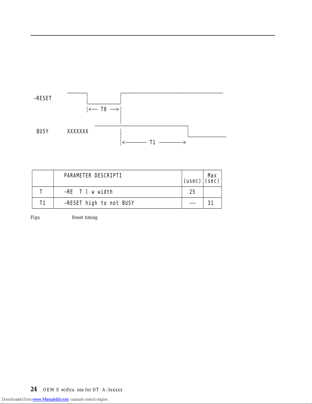
6.2.1 Reset Timings
HDD reset timing.
ДДДДДД¿ ЪДДДДДДДДДДДДДДДДДДДДДДДДДДДДДДДДД
Ä
RESET
BUSY XXXXXXX
ЪДДДДДДВДДДДДДДДДДДДДДДДДДДДДДДДДДДДДДДДДДДДДДДДДВДДДДДДВДДДДД¿
³³
³³ ³
ГДДДДДДЕДДДДДДДДДДДДДДДДДДДДДДДДДДДДДДДДДДДДДДДДДЕДДДДДДЕДДДДД´
³
T0
ГДДДДДДЕДДДДДДДДДДДДДДДДДДДДДДДДДДДДДДДДДДДДДДДДДЕДДДДДДЕДДДДД´
³
T1
АДДДДДДБДДДДДДДДДДДДДДДДДДДДДДДДДДДДДДДДДДДДДДДДДБДДДДДДБДДДДДЩ
PARAMETER DESCRIPTION
³Ä
RESET low width
³Ä
RESET high to not BUSY
³³
АДДДДДДДДДДЩ
³<ÄÄ
T0ÄÄ>
ДДДДДДДДДДДДДДДДДДДДДДДДДДДДДД¿
³
³
³
³³
³ АДДДДДДДДДДДД
³<ДДДДДДД
T1
ДДДДДДДД
>
³
Min³Max
(usec)³(sec)
³
25
³³
³Äij31³
³
³
Figure 17. System Reset timing
24 OE M Specifications fo r DTTA-3xxxxx
Page 33

6.2.2 PIO Timings
The PIO cycle timings meet Mode 4 of the ATA-3 description.
ЪДДДДДДДДДДДДДДДДДДДДДДДДДДДДДДДДДДДДДДДДД¿
Ä
CS0,ÄCS1
+DA0Ä2
Ä
DIOR,ÄDIOW
Write data
+DD00Ä15
Read data
+DD00Ä15
Ä
HIOCS16
+IORDY
ДДДДДДДД´ ГДДДДДДДДДДДД
АДДДДДДДДДДДДДДДДДДДДДДДДДДДДДДДДДДДДДДДДДЩ
³³
³<ÄÄT1Ä>³<ДДДДДДДДДДДДДДДДДT0ДДДДДДДДДДДДДДДДДД>³
ДДДДДДДДДДДДДДДД¿ ЪДДДДДДДДДДДДДД¿
³³ ³ ³³
³ АДДДДДДДДДДДДДДДДДДДДДДДДЩ ³ АДДДДДД
³³
³³ ³ ³
³ ³ ЪДДДДДДДДДДДДДДДДДДДД¿ ³
ДДДДДДДДДДДДДДДДДДДДДДДДДДД´ ГДДДДДДДДДДДДДД
³ ³ АДДДДДДДДДДДДДДДДДДДДЩ ³
³³ ³
³³ ³ ³
³ ³ ЪДДДДДДДДДДДДД¿ ³
ДДДДДДДДДДДДДДДДДДДДДДДДДДДДДД´ ГДДДДДДДДДДДДДДДДДД
³ ³ АДДДДДДДДДДДДДЩ ³
³³ ³
Ä>³
T7³<
ДДДДДДДДДДДДД¿ ³ ЪДДДДДДДДД
ДДДДДДДДДДДДДДДДДДДДДДДД¿ ЪДДДДДДДДДДДДДДДДДДДДДДДДДДДД
<
ДДДДДДДДДДT2ДДДДДДДДДД>³<ÄÄÄÄ
<
ДДДДДT3ÄÄÄÄ>³<ÄT4Ä>³³
<
ij Ä>³T8³<Ä
³³ ³
АДДДДДДДДДДДДДДДДДДДДДДДДДДДДДДДДДДДДДДДЩ
³<Ä
T10Ä>
³
³
³³
АДДДДДДДДДЩ
³<ÄÄ
T11ÄÄ>
<ÄÄT9ÄÄ>
ÄÄÄT5ДДДДДД>³T6³<ij
³
³
T2I
ДДДДД>³
ЪДДДДВДДДДДДДДДДДДДДДДДДДДДДДДДДДДДДДДДДДДДДДДДДДДДДДДВДДДДДДВДДДДДДВДДДДД¿
³³
³³ ³
ГДДДДЕДДДДДДДДДДДДДДДДДДДДДДДДДДДДДДДДДДДДДДДДДДДДДДДДЕДДДДДДЕДДДДДДЕДДДДД´
³
T0³Cycle time
³
T1
³
T2
³
T2I
³
T3³+DD00Ä15 setup toÄDIOW high
³
T4
³
T5³+DD00Ä15 setup toÄDIOR high
³
T6
³
T7
³
T8
³
T9
³
T10
³
T11³+IORDY pulse width
АДДДДБДДДДДДДДДДДДДДДДДДДДДДДДДДДДДДДДДДДДДДДДДДДДДДДДБДДДДДДБДДДДДДБДДДДДЩ
Figure 18. PI O cycle timings
Notes:
1. Apply t o ATA-2 (mode 0,1,2)
PARAMETER DESCRIPTION
³Ä
CS0Ä1, +DA00Ä02 valid toÄDIOR,ÄDIOW active
³Ä
DIOR,ÄDIOW pulse width
³Ä
DIOR,ÄDIOW recovery
³Ä
DIOW high to +DD00Ä15 hold
³Ä
DIOR high to +DD00Ä15 hold
³Ä
CS0Ä1, +DA00Ä02 valid toÄHIOCS16 assertion
³Ä
CS0Ä1, +DA00Ä02 invalid toÄHIOCS16 negation
³Ä
DIOR,ÄDIOW high toÄCS0Ä1, +DA00Ä02 hold
³Ä
DIOR,ÄDIOW low to +IORDY low
³
MIN³MAX³Note
(nsec)³(nsec)
³
120
³Ä³ ³
³
25
³Ä³ ³
³
70
³Ä³ ³
³
25
³Ä³ ³
³
20
³Ä³ ³
³
10
³Ä³ ³
³
20
³Ä³ ³
³
5
³Ä³ ³
³Ä³40³
³Ä³30³
³
10
³³³
³Ä³35³³
³Ä³
1250
³³
1
1
³³
³
³
³
Specification 25
Page 34

6.2.2.1 Write DRQ Interval Time
For write sectors a n d write multiple operations, 4.8µsec is inserted from the end of negation of the DRQ bit
until setting of th e next DRQ bi t.
6.2.2.2 Read DRQ Interval Time
For read sectors a nd read multiple operations, the interval from the end of negation of the DR Q bit until
setting of the nex t DRQ bit is as follows;
In case that a host reads the status register only before the sector or block transfer DRQ interval
DRQ interval ............ 5.2µsec.
In case that a host reads the status register after or bot h before and after th e sector or block transfer
DRQ interval ............ 14.4µsec.
26 OE M Specifications fo r DTTA-3xxxxx
Page 35

6.2.3 DMA Timings
6.2.3.1 Single Word DMA Timings
The Single Word D M A timing meets Mode 2 of the ATA-2 description.
³<ÄÄTCÄÄ>³
ЪДДДДДДДДДДД¿ ЪДДДДДДДДДДД
+DMARQ
Ä
DMACK
Ä
HIOR/ÄHIOW
READ DATA
WRITE DATA
ДДДДДДДДДДЩ ³ АДДДДДДДДДДДДДДДДДДДДДДДДДДДДЩ
ДДДДДДДДДДДДД¿ ЪДДДДДДДДДДДД¿
ДДДДДДДДДДДДДДДД¿ ЪДДДДДДДДДДДДДДДДДДДДДДДДД
ДДДДДДДДДДДДДДДДДДДДДДДДД´ ГДДДДДДДДДДДДДДДДДДДД
ДДДДДДДДДДДДДДДДДДДДДД´ ГДДДДДДДДДДДДДДДДДДДД
³³ ³ ³
³<ДДДДДДДДДДДДДДДДДT0ДДДДДДДДДДДДДДДДДД>³
³³³
АДДДДДДДДДДДДДДДДДДДДДДДДДДЩ АДДДДДДДДД
Ä>³TI³<ÄÄ
³<ДДДДДДДДTDДДДДДДДД>³
АДДДДДДДДДДДДДДДДДДДДЩ
³<ÄÄTEÄÄ>³ÄÄ
ЪДДДДДДДДДДДДДДДД¿
АДДДДДДДДДДДДДДДДЩ
³<ДДДДДTGДДДДД>³
ЪДДДДДДДДДДДДДДДДДДД¿
АДДДДДДДДДДДДДДДДДДДЩ
>³TJ³<
>³TF³<
Ä
TH³<
ÄÄ
Ä
[nsec]
ЪДДДДВДДДДДДДДДДДДДДДДДДДДДДДДДДДДДДДДДДДДДДДДДДДДДДДДВДДДДДДВДДДДДДВДДДДД¿
³³
ГДДДДЕДДДДДДДДДДДДДДДДДДДДДДДДДДДДДДДДДДДДДДДДДДДДДДДДЕДДДДДДЕДДДДДДЕДДДДД´
³
T0³Cycle time
³
TC
³
TD
³
TE
³
TF
³
TG
³
TH
³
TI
³
TJ
АДДДДБДДДДДДДДДДДДДДДДДДДДДДДДДДДДДДДДДДДДДДДДДДДДДДДДБДДДДДДБДДДДДДБДДДДДЩ
Figure 19. Single Word D M A cycle timings
PARAMETER DESCRIPTION
³Ä
DMACK active to +DMARQ inactive
³Ä
HIOR,ÄHIOW pulse width
³Ä
HIOR data access
³Ä
HIOR data hold
³Ä
HIOW data setup
³Ä
HIOW data hold
³Ä
DMACK toÄHIOR/ÄHIOW setup
³Ä
HIOR/ÄHIOW toÄDMACK hold
³
MIN³MAX³Note
³
240
³Ä³ ³
³Ä³80³³
³
120
³Ä³ ³
³Ä³60³³
³
5
³Ä³ ³
³
35
³Ä³ ³
³
20
³Ä³ ³
³
0
³Ä³ ³
³
0
³Ä³ ³
³
Specification 27
Page 36

6.2.3.2 Multiword DM A Timings
The Multiword D M A timing meets Mode 2 of the ATA-4 description.
ЪДДДДДДДДДДДДДДДДДДДДДДДДДДДДДДДДДДДДДДДДД¿
DMARQ
Ä
DMACK
Ä
HIOR/ÄHIOW
READ DATA
WRITE DATA
³³³
ДДДДЩ ³ АДДДДДДДДДДДДДДДД
ДДДДДДДДДДДД¿ ³ ³ ЪДДДДДДД
³³<ДДДДДДДДT0ДДДДДДДДДДД>³³³
АДДДДДДДДДДДДДДДДДДДДДДДДДДДДДДДДДДДДДДДДДДЩ
Ä>³TI³<ÄÄÄÄTDÄÄÄÄ>³<ÄÄÄTKÄÄÄ>³³
ДДДДДДДДДДДДДДД¿ ЪДДДДДДДДДД¿ ЪДДДДДДДДДД
³³³³
АДДДДДДДДДДДДЩ АДДДДДДДДДДДДЩ
³<ÄTEÄ>³TF³<ÄÄ
ЪДДДДДДДДД¿ ЪДДДДДДДДДДД¿
ДДДДДДДДДДДДДДДДДДДДД´ ГДДДДДДДДДДДДДД´ ГДДДД
АДДДДДДДДДЩ АДДДДДДДДДДДЩ
³<ÄÄTGÄÄ>³TH³<Ä
ЪДДДДДДДДДДД¿ ЪДДДДДДДДДДД¿
ДДДДДДДДДДДДДДДДДДД´ ГДДДДДДДДДДД´ ГДДДДДДД
АДДДДДДДДДДДЩ АДДДДДДДДДДДЩ
³<ÄTLÄ>³
³Ä
>³TJ³<
Ä
>³TZ³<
Ä
[nsec]
ЪДДДДВДДДДДДДДДДДДДДДДДДДДДДДДДДДДДДДДДДДДДДДДДДДДДДДДВДДДДДДВДДДДДДВДДДДД¿
³³
ГДДДДЕДДДДДДДДДДДДДДДДДДДДДДДДДДДДДДДДДДДДДДДДДДДДДДДДЕДДДДДДЕДДДДДДЕДДДДД´
³
T0³Cycle time
³
TD
³
TE
³
TF
³
TG
³
TH
³
TI
³
TJ
³
TK
³
TL
³
TZ
АДДДДБДДДДДДДДДДДДДДДДДДДДДДДДДДДДДДДДДДДДДДДДДДДДДДДДБДДДДДДБДДДДДДБДДДДДЩ
Figure 20. Multiword D MA cycle timings
PARAMETER DESCRIPTION
³Ä
HIOR,ÄHIOW pulse width
³Ä
HIOR data setup
³Ä
HIOR data hold
³Ä
HIOW data setup
³Ä
HIOW data hold
³Ä
DMACK toÄHIOR/ÄHIOW setup
³Ä
HIOR/ÄHIOW toÄDMACK hold
³Ä
HIOR/ÄHIOW nagated pulse width
³Ä
HIOR/ÄHIOW toÄDMARQ delay
³Ä
DMACK to tristate
³
MIN³MAX³Note
³
120
³Ä³ ³
³
70
³Ä³ ³
³
20
³Ä³ ³
³
5
³Ä³ ³
³
20
³Ä³ ³
³
10
³Ä³ ³
³
0
³Ä³ ³
³
5
³Ä³ ³
³
25
³Ä³ ³
³Ä³35³³
³Ä³25³³
³
28 OE M Specifications fo r DTTA-3xxxxx
Page 37

6.2.4 Ultra DMA Timings
The Ultra DM A timing meets Mode 0, 1 and 2 of the Ultra DMA/33 -- a Proposal for a New Protocol in
ATA/ATAPI-4 (X3T13/1153D Revision 16)
6.2.4.1 Initiating Read DMA
ЪДДДДДДДДДДДДДДДДДДДДДДДДДДДДДДДДДДДДДДДДДДДДДДДДДДДДДДДДДДДДД
DMARQ
Ä
DMACK
STOP
Ä
HDMARDY
DSTROBE
DB(15:00) XXXXXXXXXXXXXXX
³
ÄÙ
³<ÄÄ
TuiÄÄ>
ДДДДДДДДДДД¿
³
<Tack>³<Tenv>
ДДДДВДДДДДДДДДДДДД¿
³³³
ДДДДЩ ³ АДДДДДДДДДДДДДДДДДДДДДДДДДДДДДДДДДДДДДДДДДДДД
³
<Tack>³<Tenv>
ДДДДВДДДДДДДДДДДДД¿
³³³ ³
ДДДДЩ ³ АДДДДДДДДДДДДДДДДДДДДДДДДДДДДДДДДДДДДДДДДДДДД
TzrdyÄ>
ДДДДДДДДДДДДДДЩ ³ ³ ³ ³
ДДДДДДДДДДДДДД>³³
³
³
АДДДДДДДДДДДДДДДДДДДДДДДДДДДДДДДДДДДДДДДДДДДДДДДДДДД
³
³
<
ДДДДДДДДДД
³Äij<ij<ÄÄÄÄ
³ ЪДДДДДДДДДДДДДДДД¿ ЪДДДДДДДДДДДДД¿
³ ³ АДДДДДДДДДДДДДЩ ÀÄÄÄ
Taz³<Ä>
³³<Ä>³
ДДДДДДДД
Tfs
ÄÄÄ>³<ÄÄÄÄ
Tcyc
Tzad
ЪДДДДДДДДД¿ ЪДДДДДДДДД¿ ЪДДДДДДДД
XXX RD Data XXX RD Data XXX RD Data
АДДДДДДДДДЩ АДДДДДДДДДЩ АДДДДДДДД
<
ДДДДДДДДДДДДДДДДДДДДДДДДДДДДДДДДДДДДДДД
T2cyc
ÄÄÄ>³<ÄÄÄÄ
Ä>³
Tdvs³Tdvh³<
ДДДДДДДДДД>³
Tcyc
ÄÄÄ>³
Ä
Host drives DB Device drives DB
[nsec]
ЪДДДДДВДДДДДДДДДДДДДДДДДДДДДДДДДДДДДДДДДДДДДВДДДДДДДДДВДДДДДДДДДВДДДДДДДДД¿
³³ ³
³³
³³ ³
ГДДДДДЕДДДДДДДДДДДДДДДДДДДДДДДДДДДДДДДДДДДДДЕДДДДЕДДДДЕДДДДЕДДДДЕДДДДЕДДДД´
³
Tui³Unlimited interlock time
³
Tack³Setup time beforeÄDMACK assertion³20
³
Tenv³Envelope time
³
Tzrdy³Wait time before driving DSTROBE
³
Tfs³First strobe time
³
Tcyc³Cycle Time
³
T2cyc³2 Cycle time
³
Taz³Output release time
³
Tzad³Output enable time
³
Tdvs³Data setup time (at device side)
³
Tdvh³Data Hold time (at device side)
АДДДДДБДДДДДДДДДДДДДДДДДДДДДДДДДДДДДДДДДДДДДБДДДДБДДДДБДДДДБДДДДБДДДДБДДДДЩ
Figure 21. Ultra D M A cycle timings (Initiating Read)
PARAMETER DESCRIPTION
MODE0³MODE1³MODE2
ГДДДДВДДДДЕДДДДВДДДДЕДДДДВДДДД´
MIN³MAX³MIN³MAX³MIN³MAX
³
0
³Ä³0³Ä³0³Ä³
³Ä³20³Ä³20³Ä³
³
20³70³20³70³20³70
³
0
³Ä³0³Ä³0³Ä³
³
0³230³0³200³0³170
³
114
³Ä³75³Ä³55³Ä³
³
235
³Ä³
³Ä³10³Ä³10³Ä³10³
³
0
³Ä³0³Ä³0³Ä³
³
70
³Ä³48³Ä³34³Ä³
³
6
³Ä³6³Ä³6³Ä³
156
³Ä³
117
³Ä³
³
³
³
³
Specification 29
Page 38

6.2.4.2 Host Pausing Read DMA
ДДДДДДДДДДДДДДДДДДДДДДДДДДДДДДДДДДДДДДДДДДДДДДДДДДДДДДДДДДДДДДД
DMARQ
Ä
DMACK
ДДДДДДДДДДДДДДДДДДДДДДДДДДДДДДДДДДДДДДДДДДДДДДДДДДДДДДДДДДДДДДД
STOP
ДДДДДДДДДДДДДДДДДДДДДДДДДДДДДДДДДДДДДДДДДДДДДДДДДДДДДДДДДДДДДДД
³<Ä
TsrÄ>
³
³ ЪДДДДДДДДДДДДДДДДДДДДДДДДДДДДДДДДДДДДДДДДДДДДДДДДДД
Ä
HDMARDY
DSTROBE
³³
ДДДДДДДДДДДДЩ
³³
ДДДДВДДДДДДДДДДДДДДДДДДДДДДДДВДДДДДДДДДДДДДДДДДДДДДДДДДДДДДДДДД
³³
ДДДДБДДДДДДДДДДДДДДДДДДДДДДДДБДДДДДДДДДДДДДДДДДДДДДДДДДДДДДДДДД
<
ДДДДД
Trfs
ДДДДД>³
[nsec]
ЪДДДДДВДДДДДДДДДДДДДДДДДДДДДДДДДДДДДДДДДДДДДВДДДДДДДДДВДДДДДДДДДВДДДДДДДДД¿
³³ ³
³³
³³ ³
ГДДДДДЕДДДДДДДДДДДДДДДДДДДДДДДДДДДДДДДДДДДДДЕДДДДЕДДДДЕДДДДЕДДДДЕДДДДЕДДДД´
³
Tsr³Strobe to ready response time
³
Trfs³Ready to final strobe time
АДДДДДБДДДДДДДДДДДДДДДДДДДДДДДДДДДДДДДДДДДДДБДДДДБДДДДБДДДДБДДДДБДДДДБДДДДЩ
PARAMETER DESCRIPTION
MODE0³MODE1³MODE2
ГДДДДВДДДДЕДДДДВДДДДЕДДДДВДДДД´
MIN³MAX³MIN³MAX³MIN³MAX
³Ä³50³Ä³30³Ä³20³
³Ä³75³Ä³60³Ä³50³
Note : When a host does not meet Tsr, it should be ready to receive 2
more strobes after
Ä
HDMARDY is negated.
³
³
Figure 22. Ultra D M A cycle timings (Host pausing Read)
30 OE M Specifications fo r DTTA-3xxxxx
Page 39

6.2.4.3 Host Terminating Read DMA
³<ДДДДД
ДДДДДДДДДДДДДДДДДДДДДДДДДДДДДДДДД¿
DMARQ
Ä
DMACK
STOP
Ä
HDMARDY
DSTROBE
ДДДДДДДДДДДДДДДДДДДДДДДДДДДДДДДДДДДДДДДДДДДДДДДДЩ
³<ДДДДД
³ ЪДДДДДДДДДДДДДДДДДДДДДДДДДДДДДДДДДДДДДДДВДДДДД
³³ ³³³
ДДДДДДДДДДДДДДДДДЩ ³ ³ АДДДДД
³³ ³³
ЪДДДДДДДДДДДДДДДДДДДДДДДДДДДДДДДДДДДДДДДДДДДДДДДДДДДДДДВДДДДД
³³ ³³³
ÄÄÙ ³ ³ ³ АДДДДД
³<ÄÄÄ
ДДДДДДДДДДДДДДДВДДДДДДДДДДДДДДДДДВДДДДДДДДДДДДДДДДДДДД¿
ДДДДДДДДДДДДДДДБДДДДДДДДДДДДДДДДДЩ ³
¿ ЪДДДДДДДДДДДДД¿ ЪДДДДДДД¿
Trp
Trfs
ÄÄÄ>³³<ДДДДД
³³
³ АДДДДДДДДДДДДДДДДДДДДДДДДДДДДД
³³
³ ³ ЪДДДДДДДДДДДДДД
³³³
ÄÄÄÄ>³³³
³ ³ ³ АДДДДДДДД
DB(15:00) XXX RD Data XXXXXXXXXXXXXXXXXX
Ù АДДДДДДДДДДДДДЩ АДДДДДДДЩ
ДДДДДДДДДДДДДДДДДДДДДДДДДДДДДДДДДДДД>³³<ДДДДДДДДДДДДДДДДДДДДД
Tli
ДДДДД>³
<
ÄÄÄÄ
Tmli
ÄÄÄÄ>³
Tli
ДДДДД>³³
Taz³<Ä>
³
ÄÄÄÄ
³
<Tzah>
Tds³<Ä>³<Ä>³Tdh
XXX CRC XXXXXXXXXX
³
Device drives DB Host drives DB
<ÄTackÄ>
<ÄTackÄ>
<
ÄÄÄ>³
Trdyz
³
³
[nsec]
ЪДДДДДВДДДДДДДДДДДДДДДДДДДДДДДДДДДДДДДДДДДДДВДДДДДДДДДВДДДДДДДДДВДДДДДДДДД¿
³³ ³
³³
³³ ³
ГДДДДДЕДДДДДДДДДДДДДДДДДДДДДДДДДДДДДДДДДДДДДЕДДДДЕДДДДЕДДДДЕДДДДЕДДДДЕДДДД´
³
Trfs³Ready to final strobe time
³
Trp³Ready to pause time
³
Tli³Limited interlock time
³
Taz³Output release time
³
Tzah³Output enable time
³
Tmli³Interlock time
³
Tds³Data setup time (at device side)
³
Tdh³Data Hold time (at device side)
³
Tack³Hold time afterÄDMACK negation
³
Trdyz³PullÄup time before DSTROBE release
АДДДДДБДДДДДДДДДДДДДДДДДДДДДДДДДДДДДДДДДДДДДБДДДДБДДДДБДДДДБДДДДБДДДДБДДДДЩ
Figure 23. Ultra D M A cycle timings (Host terminating Read)
PARAMETER DESCRIPTION
MODE0³MODE1³MODE2
ГДДДДВДДДДЕДДДДВДДДДЕДДДДВДДДД´
MIN³MAX³MIN³MAX³MIN³MAX
³Ä³75³Ä³60³Ä³50³
³
160
³Ä³
³
0³150³0³150³0³150
³Ä³10³Ä³10³Ä³10³
³
20
³Ä³20³Ä³20³Ä³
³
20
³Ä³20³Ä³20³Ä³
³
15
³Ä³10³Ä³7³Ä³
³
5
³Ä³5³Ä³5³Ä³
³
20
³Ä³20³Ä³20³Ä³
³Ä³20³Ä³20³Ä³20³
125
³Ä³
100
³Ä³
³
³
³
Specification
31
Page 40

6.2.4.4 Device Terminating Read DMA
³<Ä>³
ДДДДДД¿
DMARQ
Ä
DMACK
STOP
Ä
HDMARDY
DSTROBE
³³
³ АДДДДДДДДДДДДДДДДДДДДДДДДДДДДДДДДДДДДДДДДДДДДДДДДДДДДДДДД
³³ ³<ÄÄÄÄ
³ ³ ³ ЪДДДДДДДДДДДДДД
³³ ³ ³
ДДДДДДДДДДДДДДДДДДДДДДДДДДДДДДДДДДДДДДДДДДДДДДДДЩ
³³<ÄÄÄ
³ ³ ЪДДДДДДДДДДДДДДДДДДДДДДДДДДДДДДДДДДДДДДДВДДДДД
³³ ³ ³ ³ ³
ДДДДДДДДДДДДДДДДДЩ ³ ³ АДДДДД
³³<ÄÄÄ
ДДДДДДДДДДДДДДДДДВДДДДДДДДДДДДДДДДДДДДДДДДДДДДДДДДДДДДДДДВДДДДД
ДДДДДДДДДДДДДДДДДЩ ³ ³ АДДДДД
³³ ³<ДДДДД
ДДВДДДДДДДДДДДДДДДДДДДДДДДДДДДДДДВДДДДДДДДДДДДДДДДДДДД¿
³ ³ ³ АДДДДДДДД
ДДБДДДДДДДДДДДДДДДДДДДДДДДДДДДДДДЩ ³
ÄÄÄÄ¿ ЪДДДДДДД¿
DB(15:00) XXXXX
ДДДДЩ АДДДДДДДЩ
ДДДДДДДДД>³³
Tss
³<Ä>³
ДДДДДДДДДДДД
³<ÄÄÄÄ
Device drives DB Host drives DB
Tmli
ÄÄÄÄ>³
TliÄÄ>
TliÄÄ>
³³³
³³³
³³³³
Tli
ДДДДД>³³
<ÄTackÄ>
<ÄTackÄ>
<
ÄÄÄ>³
Trdyz
Taz Tds³<Ä>³<Ä>³Tdh
XXXXXXXXXXXXXXXXXXXXXX CRC XXXXXXXXXX
Tzah
ÄÄÄÄ>³
<
ДДДДДДДДДДДДДДДДДДДДДДДДДДДДДДДДДДДДДДДД
³
³
[nsec]
ЪДДДДДВДДДДДДДДДДДДДДДДДДДДДДДДДДДДДДДДДДДДДВДДДДДДДДДВДДДДДДДДДВДДДДДДДДД¿
³³ ³
³³
³³ ³
ГДДДДДЕДДДДДДДДДДДДДДДДДДДДДДДДДДДДДДДДДДДДДЕДДДДЕДДДДЕДДДДЕДДДДЕДДДДЕДДДД´
³
Tss³Time from strobe to stop assertion³50
³
Tli³Limited interlock time
³
Taz³Output release time
³
Tzah³Output enable time
³
Tmli³Interlock time
³
Tds³Data setup time (at device side)
³
Tdh³Data Hold time (at device side)
³
Tack³Hold time afterÄDMACK negation
³
Trdyz³PullÄup time before DSTROBE release
АДДДДДБДДДДДДДДДДДДДДДДДДДДДДДДДДДДДДДДДДДДДБДДДДБДДДДБДДДДБДДДДБДДДДБДДДДЩ
Figure 24. Ultra D M A cycle timings (Device terminating Read)
PARAMETER DESCRIPTION
MODE0³MODE1³MODE2
ГДДДДВДДДДЕДДДДВДДДДЕДДДДВДДДД´
MIN³MAX³MIN³MAX³MIN³MAX
³Ä³50³Ä³50³Ä³
³
0³150³0³150³0³150
³Ä³10³Ä³10³Ä³10³
³
20
³Ä³20³Ä³20³Ä³
³
20
³Ä³20³Ä³20³Ä³
³
15
³Ä³10³Ä³7³Ä³
³
5
³Ä³5³Ä³5³Ä³
³
20
³Ä³20³Ä³20³Ä³
³Ä³20³Ä³20³Ä³20³
³
³
³
32 OE M Specifications fo r DTTA-3xxxxx
Page 41

6.2.4.5 Initiating Write DMA
ЪДДДДДДДДДДДДДДДДДДДДДДДДДДДДДДДДДДДДДДДДДДДДДДДДДДДДДДДДДДДДД
DMARQ
Ä
DMACK
STOP
Ä
DDMARDY
HSTROBE
³
ÄÙ
³<ÄÄ
TuiÄÄ>
ДДДДДДДДДДД¿
³
<Tack>³<Tenv>
ДДДДВДДДДДДДДДДДДД¿
³³³
ДДДДЩ ³ АДДДДДДДДДДДДДДДДДДДДДДДДДДДДДДДДДДДДДДДДДДДД
TzrdyÄ>
ДДДДДДДДДДДДДДЩ ³ ³<ДДДДДДДДДД
³
<Tack>
ДДДДВДДДДДДДДДДДДДДДДДДДДДДДДДД¿ ЪДДДДДДДДДДДДД¿
³ ³³³
ДДДДЩ АДДДДДДДДДДДДДЩ ÀÄÄÄ
³
³
АДДДДДДДДДДДДДДДДДДДДДДДДДДДДДДДДДДДДДДДДДДДДДДДДДДД
³
³Äij<ij<Ä
³ ЪДДДДДДДДДДД¿
³ АДДДДДДДДДДДДДДДДДДДДДДДДДДДДДДДДДДДД
³
TliÄ>
³
Tui³<ÄÄ>³<
ÄÄÄÄ
Tcyc
ÄÄÄ>³<ÄÄÄÄ
T2cyc
ДДДДДДДДДД>³
Tcyc
ÄÄÄ>³
Tds³<ÄÄ>³<ÄÄ>³Tdh
ЪДДДДДДДДД¿ ЪДДДДДДДДД¿ ЪДДДДДДДД
DB(15:00) XXXXXXXXXXXXXXXXXXXXXXXXXX WT Data XXX WT Data XXX WT Data
АДДДДДДДДДЩ АДДДДДДДДДЩ АДДДДДДДД
<
ДДДДДДДДДДДДДДДДДДДДДД
Host drives DB
ДДДДДДДДДДДДДДДДДДДДДДД
>
[nsec]
ЪДДДДДВДДДДДДДДДДДДДДДДДДДДДДДДДДДДДДДДДДДДДВДДДДДДДДДВДДДДДДДДДВДДДДДДДДД¿
³³ ³
³³
³³ ³
ГДДДДДЕДДДДДДДДДДДДДДДДДДДДДДДДДДДДДДДДДДДДДЕДДДДЕДДДДЕДДДДЕДДДДЕДДДДЕДДДД´
³
Tui³Unlimited interlock time
³
Tack³Setup time beforeÄDMACK assertion³20
³
Tenv³Envelope time
³
Tzrdy³Wait time before driving DSTROBE
³
Tli³Limited interlock time
³
Tcyc³Cycle Time
³
T2cyc³2 Cycle time
³
Tds³Data setup time (at device side)
³
Tdh³Data Hold time (at device side)
АДДДДДБДДДДДДДДДДДДДДДДДДДДДДДДДДДДДДДДДДДДДБДДДДБДДДДБДДДДБДДДДБДДДДБДДДДЩ
Figure 25. Ultra D M A cycle timings (Initiating Write)
PARAMETER DESCRIPTION
MODE0³MODE1³MODE2
ГДДДДВДДДДЕДДДДВДДДДЕДДДДВДДДД´
MIN³MAX³MIN³MAX³MIN³MAX
³
0
³Ä³0³Ä³0³Ä³
³Ä³20³Ä³20³Ä³
³
20³70³20³70³20³70
³
0
³Ä³0³Ä³0³Ä³
³
0³150³0³150³0³150
³
114
³Ä³75³Ä³55³Ä³
³
235
³Ä³
³
15
³Ä³10³Ä³7³Ä³
³
5
³Ä³5³Ä³5³Ä³
156
³Ä³
117
³Ä³
³
³
³
³
Specification
33
Page 42

6.2.4.6 Device Pausing Write D MA
ДДДДДДДДДДДДДДДДДДДДДДДДДДДДДДДДДДДДДДДДДДДДДДДДДДДДДДДДДДДДДДД
DMARQ
Ä
DMACK
ДДДДДДДДДДДДДДДДДДДДДДДДДДДДДДДДДДДДДДДДДДДДДДДДДДДДДДДДДДДДДДД
STOP
ДДДДДДДДДДДДДДДДДДДДДДДДДДДДДДДДДДДДДДДДДДДДДДДДДДДДДДДДДДДДДДД
³<Ä
TsrÄ>
³
³ ЪДДДДДДДДДДДДДДДДДДДДДДДДДДДДДДДДДДДДДДДДДДДДДДДДДД
Ä
DDMARDY
HSTROBE
³³
ДДДДДДДДДДДДЩ
³³
ДДДДВДДДДДДДДДДДДДДДДДДДДДДДДВДДДДДДДДДДДДДДДДДДДДДДДДДДДДДДДДД
³³
ДДДДБДДДДДДДДДДДДДДДДДДДДДДДДБДДДДДДДДДДДДДДДДДДДДДДДДДДДДДДДДД
<
ДДДДД
Trfs
ДДДДД>³
[nsec]
ЪДДДДДВДДДДДДДДДДДДДДДДДДДДДДДДДДДДДДДДДДДДДВДДДДДДДДДВДДДДДДДДДВДДДДДДДДД¿
³³ ³
³³
³³ ³
ГДДДДДЕДДДДДДДДДДДДДДДДДДДДДДДДДДДДДДДДДДДДДЕДДДДЕДДДДЕДДДДЕДДДДЕДДДДЕДДДД´
³
Tsr³Strobe to ready response time
³
Trfs³Ready to final strobe time
АДДДДДБДДДДДДДДДДДДДДДДДДДДДДДДДДДДДДДДДДДДДБДДДДБДДДДБДДДДБДДДДБДДДДБДДДДЩ
PARAMETER DESCRIPTION
MODE0³MODE1³MODE2
ГДДДДВДДДДЕДДДДВДДДДЕДДДДВДДДД´
MIN³MAX³MIN³MAX³MIN³MAX
³Ä³50³Ä³30³Ä³20³
³Ä³75³Ä³60³Ä³50³
Note : When a device does not meet Tsr, it shall be ready to receive 2
more strobes after
Ä
DDMARDY is negated.
³
³
Figure 26. Ultra D M A cycle timings (Device pausing Write)
34 OE M Specifications fo r DTTA-3xxxxx
Page 43

6.2.4.7 Device Terminating Write D MA
DMARQ
Ä
DMACK
STOP
Ä
DDMARDY
HSTROBE
³<ДДДДД
ДДДДДДДДДДДДДДДДД¿
³³
³ АДДДДДДДДДДДДДДДДДДДДДДДДДДДДДДДДДДДДДДДДДДДДД
³³ ³
³ ³ ³ ЪДДДДДДДДДДДДДД
³³ ³³
ДДДДДДДДДДДДДДДДДДДДДДДДДДДДДДДДДДДДДДДДДДДДДДДДЩ
³³ ³³
³ ³ ЪДДДДДДДДДДДДДДДДДДДДДДДВДДДДД
³³ ³³³
ДДДДДДДДДДДДДДДДДДДДДДДДДДДДДДДДДЩ ³ АДДДДД
³³ ³³
ЪДДДДДДДДДДДДДДДДДДДДДДДДДДДДДДДДДДДДДДДДДДДДДДДДДДД¿
³ ³ ³ ³ АДДДДДДДД
ÄÄÙ ³ ³ ³
³<ÄÄÄ
ДДДДДДДДДДДДДДДВДДДДДДДДДДДДДДДДДВДДДДДДДДДДДДДДДДДДДДДДДВДДДДД
ДДДДДДДДДДДДДДДБДДДДДДДДДДДДДДДДДЩ ³ АДДДДД
Trp
ÄÄÄÄ>³
Trfs
ÄÄÄ>³³<ДДДДД
<
ÄÄÄÄ
Tmli
ÄÄÄÄ>³
<ÄTackÄ>
<
ÄÄÄ>³
Tli
ДДДДД>³³
³³³³
<ÄTackÄ>
³
Trdyz
³
Tds³<Ä>³<Ä>³Tdh
¿ ЪДДДДДДДДДДДДД¿ ЪДДДДДДД¿
DB(15:00) XXX WT Data XXXXXXXXXXXXXXXXXXXXXXXXX CRC XXXXXXXXXX
Ù АДДДДДДДДДДДДДЩ АДДДДДДДЩ
<
ДДДДДДДДДДДДДДДДДДДДДД
Host drives DB
ДДДДДДДДДДДДДДДДДДДДДДД
>
[nsec]
ЪДДДДДВДДДДДДДДДДДДДДДДДДДДДДДДДДДДДДДДДДДДДВДДДДДДДДДВДДДДДДДДДВДДДДДДДДД¿
³³ ³
³³
³³ ³
ГДДДДДЕДДДДДДДДДДДДДДДДДДДДДДДДДДДДДДДДДДДДДЕДДДДЕДДДДЕДДДДЕДДДДЕДДДДЕДДДД´
³
Trfs³Ready to final strobe time
³
Trp³Ready to pause time
³
Tli³Limited interlock time
³
Tmli³Interlock time
³
Tds³Data setup time (at device side)
³
Tdh³Data Hold time (at device side)
³
Tack³Hold time afterÄDMACK negation
³
Trdyz³PullÄup time before HSTROBE release
АДДДДДБДДДДДДДДДДДДДДДДДДДДДДДДДДДДДДДДДДДДДБДДДДБДДДДБДДДДБДДДДБДДДДБДДДДЩ
Figure 27. Ultra D M A cycle timings (Device terminating Write)
PARAMETER DESCRIPTION
MODE0³MODE1³MODE2
ГДДДДВДДДДЕДДДДВДДДДЕДДДДВДДДД´
MIN³MAX³MIN³MAX³MIN³MAX
³Ä³75³Ä³60³Ä³50³
³
160
³Ä³
³
0³150³0³150³0³150
³
20
³Ä³20³Ä³20³Ä³
³
15
³Ä³10³Ä³7³Ä³
³
5
³Ä³5³Ä³5³Ä³
³
20
³Ä³20³Ä³20³Ä³
³Ä³20³Ä³20³Ä³20³
125
³Ä³
100
³Ä³
³
³
³
Specification
35
Page 44

6.2.4.8 Host Terminating Write DMA
³<ÄÄÄ
DMARQ
Ä
DMACK
STOP
Ä
DDMARDY
HSTROBE
TliÄÄ>
ДДДДДДДДДДДДДДДДД¿
³³
³ АДДДДДДДДДДДДДДДДДДДДДДДДДДДДДДДДДДДДДДДДДДДДД
³³ ³
³ ³ ³ ЪДДДДДДДДДДДДДД
³³ ³ ³
ДДДДДДДДДДДДДДДДДДДДДДДДДДДДДДДДДДДДДДДДДДДДДДДДЩ
³<Ä>³
³ ЪДДДДДДДДДДДДДДДДДДДДДДДДДДДДДДДДДДДДДДДДДДДДДДДДДДВДДДДД
³³ ³ ³ ³ ³
ДДДДДДЩ ³ ³ ³ АДДДДД
³³<ÄÄÄ
³ ЪДДДДДДДДДДДДДДДДДДДДДДДДДДДДДДДДДДДД¿
³ ³ ³ ³ АДДДДДДДД
ДДДДДДДДДДДДДДДДДЩ ³ ³
³³
ДДВДДДДДДДДДДДДДДДДДДДДДДДДДДДДДДВДДДДДДДДДДДДДДДДДДДДДДДВДДДДД
³³³³
ДДБДДДДДДДДДДДДДДДДДДДДДДДДДДДДДДЩ ³ АДДДДД
Tss
TliÄÄ>
³
<
ÄÄÄÄ
Tmli
ÄÄÄÄ>³
³³³
³³³
<
ДДДДД
Tli
ДДДДД>³³
<ÄTackÄ>
<
ÄÄÄ>³
Trdyz
<ÄTackÄ>
³
³
Tds³<Ä>³<Ä>³Tdh
ÄÄÄÄ¿ ЪДДДДДДД¿
DB(15:00) XXXXXXXXXXXXXXXXXXXXXXXXXXXXXXXXXXXXXXX CRC XXXXXXXXXX
ДДДДЩ АДДДДДДДЩ
<
ДДДДДДДДДДДДДДДДДДДДДД
Host drives DB
ДДДДДДДДДДДДДДДДДДДДДДД
>
[nsec]
ЪДДДДДВДДДДДДДДДДДДДДДДДДДДДДДДДДДДДДДДДДДДДВДДДДДДДДДВДДДДДДДДДВДДДДДДДДД¿
³³ ³
³³
³³ ³
ГДДДДДЕДДДДДДДДДДДДДДДДДДДДДДДДДДДДДДДДДДДДДЕДДДДЕДДДДЕДДДДЕДДДДЕДДДДЕДДДД´
³
Tss³Time from strobe to stop assertion³50
³
Tli³Limited interlock time
³
Tmli³Interlock time
³
Tds³Data setup time (at device side)
³
Tdh³Data Hold time (at device side)
³
Tack³Hold time afterÄDMACK negation
³
Trdyz³PullÄup time before DSTROBE release
АДДДДДБДДДДДДДДДДДДДДДДДДДДДДДДДДДДДДДДДДДДДБДДДДБДДДДБДДДДБДДДДБДДДДБДДДДЩ
Figure 28. Ultra D M A cycle timings (Host terminating Write)
PARAMETER DESCRIPTION
MODE0³MODE1³MODE2
ГДДДДВДДДДЕДДДДВДДДДЕДДДДВДДДД´
MIN³MAX³MIN³MAX³MIN³MAX
³Ä³50³Ä³50³Ä³
³
0³150³0³150³0³150
³
20
³Ä³20³Ä³20³Ä³
³
15
³Ä³10³Ä³7³Ä³
³
5
³Ä³5³Ä³5³Ä³
³
20
³Ä³20³Ä³20³Ä³
³Ä³20³Ä³20³Ä³20³
³
³
³
36 OE M Specifications fo r DTTA-3xxxxx
Page 45

6.2.5 Addressing of HDD Registers
The host addresses the drive through a set of registers called the Task File. These registers a r e mapped into
the host's I /O space. Tw o chi p select lines (-CS0 a nd -CS1) and three address lines (DA00-02) are used t o
select on e of these registers, while a -DIOR or -DIOW is provided at the specified time.
The -CS0 is used to address Command Block registers. while the -CS1 is used to address Control Block
registers.
The following table shows t he I/ O address map.
ЪДДДДДВДДДДДВДДДДВДДДДВДДДДВДДДДДДДДДДДДДДДДДДДВДДДДДДДДДДДДДДДДДДДДД¿
³Ä
CS0³ÄCS1³DA02³DA01³DA00
ГДДДДДЕДДДДДЕДДДДЕДДДДЕДДДДЕДДДДДДДДДДДДДДДДДДДБДДДДДДДДДДДДДДДДДДДДД´
³ ³ ³³³³
ГДДДДДЕДДДДДЕДДДДЕДДДДЕДДДДЕДДДДДДДДДДДДДДДДДДДВДДДДДДДДДДДДДДДДДДДДД´
³
0
³
1
³
0
³
0
³
³
0
³
1
³
0
³
0
³
³
0
³
1
³
0
³
1
³
³
0
³
1
³
0
³
1
³
³
0
³
1
³
1
³
0
³
³
0
³
1
³
1
³
0
³
0
³
1
³
1
³
1
³
³
0
³
1
³
1
ГДДДДДЕДДДДДЕДДДДЕДДДДЕДДДДЕДДДДДДДДДДДДДДДДДДДБДДДДДДДДДДДДДДДДДДДДД´
³ ³ ³³³³
ГДДДДДЕДДДДДЕДДДДЕДДДДЕДДДДЕДДДДДДДДДДДДДДДДДДДВДДДДДДДДДДДДДДДДДДДДД´
³
1
³
0
³
1
³
1
³
0
³
1
АДДДДДБДДДДДБДДДДБДДДДБДДДДБДДДДДДДДДДДДДДДДДДДБДДДДДДДДДДДДДДДДДДДДДЩ
³
³
1
³
³
1
³
³
1
³
³Ä
DIOR = 0 (Read)
³Ä
DIOW = 0 (Write)
Command Block Registers
0³Data Reg.
1³Error Reg.
³
Data Reg.
³
Features Reg.
0³Sector count Reg.³Sector count Reg.
1³Sector number Reg.³Sector number Reg
0³Cylinder low Reg.³Cylinder low Reg.
1³Cylinder high Reg.³Cylinder high Reg.
0³Drive/Head Reg.³Drive/Head Reg.
1³Status Reg.
³
Command Reg.
Control Block Registers
0³Alt. Status Reg.³Device control Reg
1³Drive address Reg.
³Ä ³
³
³
³
³
³
³
³
³
³
³
³
³
Figure 29. I/O address map
Note: "Addr." field is shown just as an example.
During DM A operation (from writing to the command register until an interrupt), all registers are no t accessible.
For example, the host is n ot supposed t o read status register contents before interrupt (the value is invalid).
6.2.6 Cabling
The maximum cable length from the host system to th e HD D plus circuit pattern length in th e host system
shall not exceed 18 inches.
For higher d a ta transfer application(>8.3MB/sec), a consideration in system design is recommended to
reduce cable noise and/or cross-talk, such as shorter cable, bus termination, shielded cable, etc.
Specification 37
Page 46
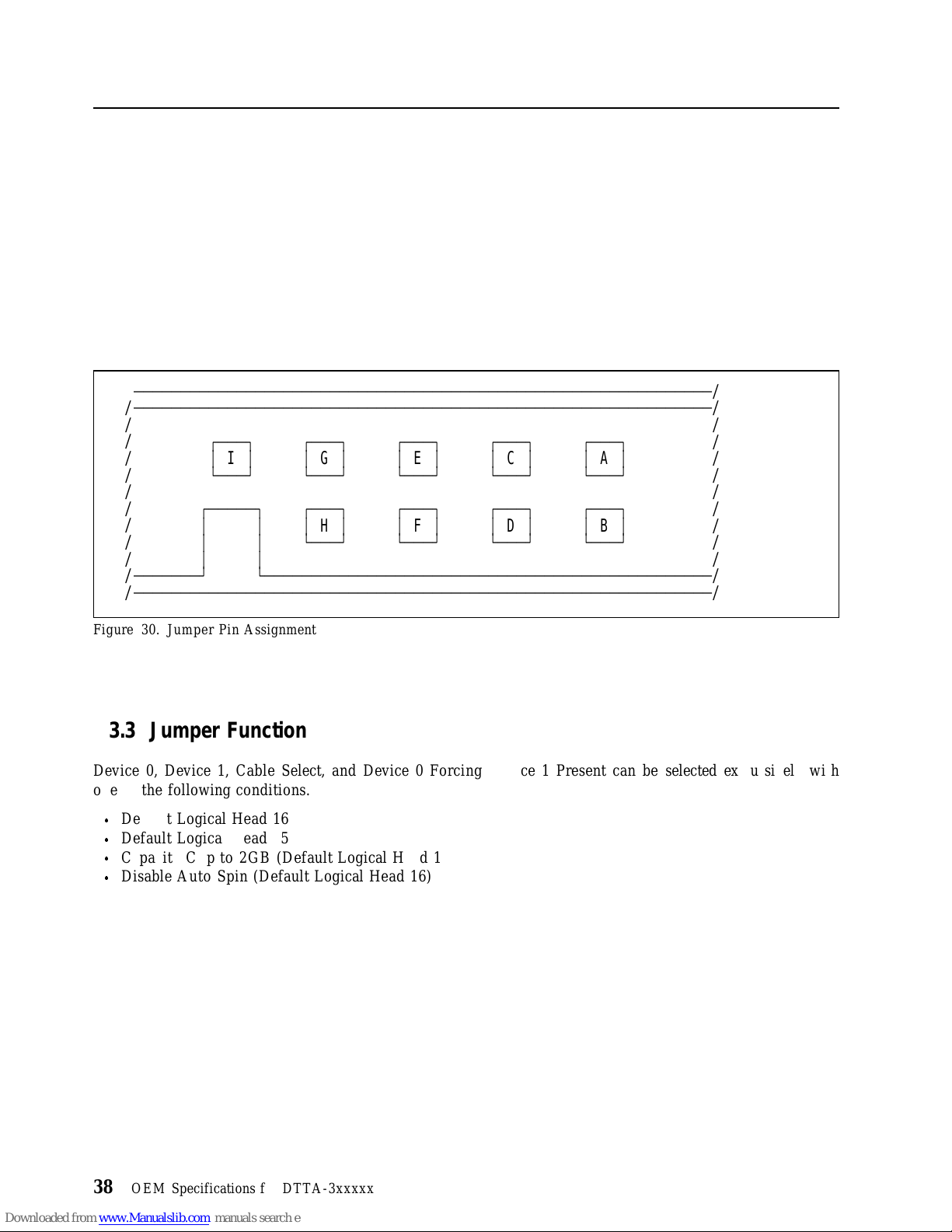
6.3 Jumper Settings
6.3.1 Location of Jumper Pin
Jumper pins are located between power pins and AT interface pins.
Refer t o 6.7.3, “ Connector Locations” o n page 51 for location of the jumper pins. Pin position A is indicated in the figure.
6.3.2 Jumper Pin Assignment
Pin number A through I are prepared for jumper setting.
/
ДДДДДДДДДДДДДДДДДДДДДДДДДДДДДДДДДДДДДДДДДДДДДДДДДДДДДДДДДДДДДД
/
ДДДДДДДДДДДДДДДДДДДДДДДДДДДДДДДДДДДДДДДДДДДДДДДДДДДДДДДДДДДДДД
/ /
/
/
/
ÚÄÄÄ¿ ÚÄÄÄ¿ ÚÄÄÄ¿ ÚÄÄÄ¿ ÚÄÄÄ¿
³I³³G³³E³³C³³A³
АДДДЩ АДДДЩ АДДДЩ АДДДЩ АДДДЩ
/ /
/
/
/
/
/
ДДДДДДДЩ АДДДДДДДДДДДДДДДДДДДДДДДДДДДДДДДДДДДДДДДДДДДДДДДД
/
ДДДДДДДДДДДДДДДДДДДДДДДДДДДДДДДДДДДДДДДДДДДДДДДДДДДДДДДДДДДДДД
ЪДДДДД¿ ÚÄÄÄ¿ ÚÄÄÄ¿ ÚÄÄÄ¿ ÚÄÄÄ¿
³³³H³³F³³D³³B³
³ ³ АДДДЩ АДДДЩ АДДДЩ АДДДЩ
³³
/
/
/
/
/
/
/
/
/
/
/
Figure 30. Jumper Pin Assignment
6.3.3 Jumper Function
Device 0, Device 1, Cable Select, and Device 0 Forcing Device 1 Present can be selected exclussively with
one of the following conditions.
Default Logical Hea d 16
Default Logical Head 15
Capacity Clip to 2GB (Default Logical Hea d 16)
Disable Auto Spin (Default Logical Head 16)
38 OE M Specifications fo r DTTA-3xxxxx
Page 47

6.3.4 Jumper Set Position
6.3.4.1 For Default Logical Head 16
ДДДДДДДДДДДДДДДДДДДДДДДДДДДДДДДДД
ÚÄ¿ ÚÄ¿
I
³G³
³³ ³³
³H³
ÀÄÙ ÀÄÙ
ДДДДДДДДДДДДДДДДДДДДДДДДДДДДДДДДД
ДДДДДДДДДДДДДДДДДДДДДДДДДДДДДДДДД
IGE
HF
ДДДДДДДДДДДДДДДДДДДДДДДДДДДДДДДДД
ДДДДДДДДДДДДДДДДДДДДДДДДДДДДДДДДД
IG
H
ДДДДДДДДДДДДДДДДДДДДДДДДДДДДДДДДД
ДДДДДДДДДДДДДДДДДДДДДДДДДДДДДДДДД
ÚÄ¿ ÚÄ¿
I
³G³³E³
³³ ³³
³H³³F³
ÀÄÙ ÀÄÙ
ДДДДДДДДДДДДДДДДДДДДДДДДДДДДДДДДД
EC
FD
ÚÄ¿ ÚÄ¿
³C³³A³
³³ ³³
³D³³B³
ÀÄÙ ÀÄÙ
ÚÄ¿ ÚÄ¿
³E³
³³ ³³
³F³
ÀÄÙ ÀÄÙ
³A³
³B³
C
³A³
D
³B³
CA
D B Forcing DEVICE 1 PRESENT
DEVICE 0 <ÄÄShipping Default
except
DTTAÄ350640/350430
DEVICE 1
CABLE SELECT
DEVICE 0
Figure 31. Jumper Block Setting Position
Notes:
1. All other setting patterns are reserved. D o not make other setting.
2. When CABLE SELECT is specified, AT interface signal #28 CSEL is referred to determin the drive
address as follows:
When CSEL is grounded or at a low level, the drive address is 0 (Device0).
When CSEL is open or at a high level, t he drive address is 1 (Device1).
Specification 39
Page 48

6.3.4.2 For Default Logical Head 15
ДДДДДДДДДДДДДДДДДДДДДДДДДДДДДДДДД
ÚÄ¿ ЪДДДДДДД¿
I
³G³
³ ³ АДДДДДДДЩ
³H³
ÀÄÙ
ДДДДДДДДДДДДДДДДДДДДДДДДДДДДДДДДД
ДДДДДДДДДДДДДДДДДДДДДДДДДДДДДДДДД
IGE
E
³
CA³DEVICE 0 <ÄÄShipping Default
F D B DTTAÄ350640/350430
ЪДДДДДДД¿
³
CA
АДДДДДДДЩ
HFDB
ДДДДДДДДДДДДДДДДДДДДДДДДДДДДДДДДД
ДДДДДДДДДДДДДДДДДДДДДДДДДДДДДДДДД
ÚÄ¿ ЪДДДДДДД¿
IG
H
ДДДДДДДДДДДДДДДДДДДДДДДДДДДДДДДДД
ДДДДДДДДДДДДДДДДДДДДДДДДДДДДДДДДД
ÚÄ¿ ÚÄ¿ ЪДДДДДДД¿
I
³G³³E³³
³ ³ ³ ³ АДДДДДДДЩ
³H³³F³
ÀÄÙ ÀÄÙ
ДДДДДДДДДДДДДДДДДДДДДДДДДДДДДДДДД
³E³³
³ ³ АДДДДДДДЩ
³F³
ÀÄÙ
CA
DB
CA
D B Forcing DEVICE 1 PRESENT
for
³
DEVICE 1
³
CABLE SELECT
³
DEVICE 0
Figure 32. Jumper Block Setting Position
Notes:
1. All other setting patterns are reserved. D o not make other setting.
2. When CABLE SELECT is specified, AT interface signal #28 CSEL is referred to determin the drive
address as follows:
When CSEL is grounded or at a low level, the drive address is 0 (Device0).
When CSEL is open or at a high level, t he drive address is 1 (Device1).
40 OE M Specifications fo r DTTA-3xxxxx
Page 49

6.3.4.3 For Capacity Clip to 2 GB with Default Logical Head 16
ДДДДДДДДДДДДДДДДДДДДДДДДДДДДДДДДД
ÚÄ¿
I
³G³
³³
³ ³ ЪДДДДДДД¿
³H³
ÀÄÙ АДДДДДДДЩ
ДДДДДДДДДДДДДДДДДДДДДДДДДДДДДДДДД
ДДДДДДДДДДДДДДДДДДДДДДДДДДДДДДДДД
ECA
F
³
DB
³
DEVICE 0
IGECA
DEVICE 1
ЪДДДДДДД¿
HF
ДДДДДДДДДДДДДДДДДДДДДДДДДДДДДДДДД
ДДДДДДДДДДДДДДДДДДДДДДДДДДДДДДДДД
ÚÄ¿
IG
ДДДДДДДДДДДДДДДДДДДДДДДДДДДДДДДДД
ДДДДДДДДДДДДДДДДДДДДДДДДДДДДДДДДД
ÚÄ¿ ÚÄ¿
I
³G³³E³
³³ ³³
³ ³ ³ ³ ЪДДДДДДД¿
³H³³F³³
ÀÄÙ ÀÄÙ АДДДДДДДЩ
ДДДДДДДДДДДДДДДДДДДДДДДДДДДДДДДДД
³E³
³³
³ ³ ЪДДДДДДД¿
H
³F³³
ÀÄÙ АДДДДДДДЩ
³
DB
АДДДДДДДЩ
³
CA
DB
³
CA
DB
³
CABLE SELECT
DEVICE 0
Forcing DEVICE 1 PRESENT
Figure 33. Jumper Block Setting Position
Notes:
1. All other setting patterns are reserved. D o not make other setting.
2. When CABLE SELECT is specified, AT interface signal #28 CSEL is referred to determin the drive
address as follows:
When CSEL is grounded or at a low level, the drive address is 0 (Device0).
When CSEL is open or at a high level, t he drive address is 1 (Device1).
Specification 41
Page 50

6.3.4.4 For Disabling Auto Spin with Default Logical Head 16
ДДДДДДДДДДДДДДДДДДДДДДДДДДДДДДДДД
ÚÄ¿ ЪДДДДДДД¿
I
³G³
³ ³ АДДДДДДДЩ
³ ³ ЪДДДДДДД¿
³H³
ÀÄÙ АДДДДДДДЩ
ДДДДДДДДДДДДДДДДДДДДДДДДДДДДДДДДД
ДДДДДДДДДДДДДДДДДДДДДДДДДДДДДДДДД
IGE
HF
ДДДДДДДДДДДДДДДДДДДДДДДДДДДДДДДДД
ДДДДДДДДДДДДДДДДДДДДДДДДДДДДДДДДД
IG
H
ДДДДДДДДДДДДДДДДДДДДДДДДДДДДДДДДД
ДДДДДДДДДДДДДДДДДДДДДДДДДДДДДДДДД
ÚÄ¿ ÚÄ¿ ЪДДДДДДД¿
I
³G³³E³³
³ ³ ³ ³ АДДДДДДДЩ
³ ³ ³ ³ ЪДДДДДДД¿
³H³³F³³
ÀÄÙ ÀÄÙ АДДДДДДДЩ
ДДДДДДДДДДДДДДДДДДДДДДДДДДДДДДДДД
E
³
CA
F
³
DB
ЪДДДДДДД¿
³
CA
АДДДДДДДЩ
ЪДДДДДДД¿
³
DB
АДДДДДДДЩ
ÚÄ¿ ЪДДДДДДД¿
³E³³
³ ³ АДДДДДДДЩ
³ ³ ЪДДДДДДД¿
³F³³
ÀÄÙ АДДДДДДДЩ
CA
DB
CA
DB
³
DEVICE 0
³
³
DEVICE 1
³
³
CABLE SELECT
³
³
DEVICE 0
Forcing DEVICE 1 PRESENT
³
Figure 34. Jumper Block Setting Position
Notes:
1. All other setting patterns are reserved. D o not make other setting.
2. When CABLE SELECT is specified, AT interface signal #28 CSEL is referred to determin the drive
address as follows:
When CSEL is grounded or at a low level, the drive address is 0 (Device0).
When CSEL is open or at a high level, t he drive address is 1 (Device1).
42 OE M Specifications fo r DTTA-3xxxxx
Page 51

6.4 Environment
Figure 35. Environmental Condition
Operating Conditions
Temperature 5 to 55˚C (See note)
Relative Humidity 8 to 90 %RH non-condensing
Maximum Wet Bulb Temperature 29.4˚C non-condensing
Maximum Temperature Gradient 15˚C / Hour
Altitude − 300 to 3048 m
Non-Operating Conditions
Temperature − 40 to 65˚C
Relative Humidity 5 to 95 %RH non-condensing
Maximum Wet Bulb Temperature 35˚C non-condensing
Maximum Temperature Gradient 15˚C / Hour
Altitude − 300 to 12,000 m
Note:
The system has t o provide sufficient ventilation to maintain a surface temperature below 60˚C at the
center of the top cover of the drive.
Non-operating condition should no t continue beyond one year.
Specification 43
Page 52

6.5 DC Power Requirements
Connection to the product should be made in isolated secondary circuits (SELV). T h e following voltage
specification is applied at the power connector of the drive. Damage t o the file electronics may result if t h e
power supply cable is connected or disconnected while power is being applied to th e file (Hot plug/unplug is
not allowed). There is no special power on/off sequencing required.
Figure 36. Input Voltage
During run and spin up Absolute max voltage
+ 5 Volts Supply 5V +/-5% 7V
+12 Volts Supply DTTA-35xxxx 12V +10%,-8%
DTTA-37xxxx 12V +/-5%
Figure 37. Power Supply Current of DTTA-37xxxx
+5Volts +12Volts Total
(All values in Amps.)
Idle Average 0.29 0.02 0.45 0.1 6.9
Idle ripple (peak-to-peak) 0.25 0.04 0.7 0.15
Seek peak 0.55 0.02 1.7 0.2
Seek average (*1) 0.33 0.02 0.7 0.1 10.1
Start u p (max) 0.7 0.02 2 0.1
R ND R /W peak 0.8 0.15 0.75 0.1
RND R/W average (*2) 0.42 0.15 0.65 0.1 9.9
Standby/Sleep average 0.165 0.01 0.0045 0.001 0.9
Figure 38. Power Supply Current of DTTA-351680/351350/351290
(All values in Amps.)
Pop Mean Std.Dev Pop Mean Std.Dev
+5Volts +12Volts Total
Pop Mean Std.Dev Pop Mean Std.Dev
15V
(W)
(W)
Idle Average 0.29 0.02 0.29 0.1 4.9
Idle ripple (peak-to-peak) 0.25 0.04 0.6 0.15
Seek peak 0.55 0.02 1.6 0.2
Seek average (*1) 0.33 0.02 0.6 0.1 8.9
Start u p (max) 0.7 0.02 2 0.1
R ND R /W peak 0.8 0.15 0.65 0.1
RND R/W average (*2) 0.42 0.15 0.55 0.1 8.7
Standby/Sleep average 0.165 0.01 0.0045 0.001 0.9
44 OE M Specifications fo r DTTA-3xxxxx
Page 53

Figure 39. Power Supply Current of DTTA-351010/350840/350640/350430/350320
+5Volts +12Volts Total
(All values in Amps.)
Pop Mean Std.Dev Pop Mean Std.Dev
Idle Average 0.29 0.02 0.16 0.05 3.4
Idle ripple (peak-to-peak) 0.22 0.04 0.3 0.1
Seek peak 0.5 0.02 1.23 0.2
Seek average (*1) 0.33 0.02 0.37 0.1 6.1
Start u p (max) 0.7 0.02 1.2 0.1
R ND R /W peak 0.6 0.15 0.38 0.1
RND R/W average (*2) 0.42 0.15 0.34 0.1 6.2
Standby/Sleep average 0.165 0.01 0.0045 0.001 0.9
Notes:
1. Random Seeks at 4 0% duty cycle.
2. Seek Duty = 30%, W/ R Duty = 45%, Idle Duty = 25%.
Figure 40. Power Supply Generated Ripple as seen a t file power connector
(W)
Maximum Notes
+5V DC 100 [m V pp] 0-10 [MHz]
+12V DC 150 [m V pp] 0-10 [MHz]
During file start up an d seeking, 12 volt ripple is generated b y the file (referred to as dynamic loading). If
several files have their power daisy chained together t hen the power supply ripple plus other file's dynamic
loading must remain within the above regulation tolerance. A common supply with separate power leads t o
each file is a more desirable method of power distribution.
To prevent external electrical noise from interfering with the file's performance, the file must be held by four
screws in a user system frame which h as n o electrical level difference at the four screws position, and has less
than +/-300 millivolts peak t o peak level difference to the file power connector ground.
Specification 45
Page 54

6.5.1 Start Up Current
6.5.1.1 DTTA-351010/350840/350640/350430/350320
Figure 41. Typical Current Wave Form of 12V at Start U p of DTTA-351010/350840/350640/350430/350320.
|
6.5.1.2 DTTA-351680/351350/351290
| Figure 42. Typical Current Wave Form of 12V at Start U p of DTTA-351680/351350/351290.
46 OE M Specifications fo r DTTA-3xxxxx
Page 55

6.5.1.3 DTTA-371440/371290/371010
Figure 43. Typical Current Wave Form of 12V at Start U p of DTTA-371440/371290/371010.
Specification
47
Page 56

6.6 Reliability
6.6.1 Contact Start Stop (CSS)
The drive is designed to withstand a minimum of 40,000 contact start/stop cycles at 40˚C with 13-25% relative humidity.
The drive is designed to withstand a minimum of 10,000 contact start/stop cycles at operating environment
conditions specified in 6.4, “ Environment” on page 43.
6.6.2 Preventive Maintenance
None.
6.6.3 Data Reliability
Probability of n ot recovering data ....... 1 in 1013bits read
EC C implementation
On-The-Fly correction, performed as a part of read channel function, recovers up to 12 symbols of error
in 1 sector. (1 symbol is 8 bits.)
6.6.4 Cable Noise Interference
To avoid a ny degradation of performance throughput or error when the interface cable is routed o n to p or
comes in contact with the HDA assembly, th e drive must be grounded electrically to the system frame by
four screws. The common mode noise or voltage level difference between t he system frame and power cable
ground or AT interface cable ground should be in the allowable level specified in th e power requirement
section.
48 OE M Specifications fo r DTTA-3xxxxx
Page 57

6.7 Mechanical Specifications
6.7.1 Outline
Figure 44. Outline of DTTA-3xxxxx
6.7.2 Mechanical Dimensions and Weight
The following chart describes the dimensions for the 3.5" hard disk drive form factor.
DTTA-371440
| DTTA-351350
Height (m m ) 25.4 ± 0.4 25.4 ± 0.4 25.4 ± 0.4
Width (mm) 101.6 ± 0.4 101.6 ± 0.4 101.6 ± 0.4
Length (mm) 146.0 ± 0.6 146.0 ± 0.6 146.0 ± 0.6
Weight (gram) 630 Max 630 Max 530 Max
Figure 45. Physical Dimension an d Weight
DTTA-371290
DTTA-371010
DTTA-351680
DTTA-351290
DTTA-351010
DTTA-350840
DTTA-350640
DTTA-350430
DTTA-350320
Specification 49
Page 58

Figure 46. Mechanical Dimension
50 OE M Specifications fo r DTTA-3xxxxx
Page 59

6.7.3 Connector Locations
Figure 47. Connector Locations
Specification
51
Page 60

6.7.4 Hole Locations
The Figure 48 on page 52 shows t he outline of DTTA-3xxxxx which includes the hole locations.
Figure 48. Mounting Positions an d the Tappings
52 OE M Specifications fo r DTTA-3xxxxx
Page 61

6.7.5 Mounting Orientation
The drive will operate in all axes (6 directions). T he drive will operate within the specified error rates when
tilted ± 5 degree from these positions.
Performance and error rate will stay within specification limits if the drive is operated in the other permissible orientat ion s from which it was formatted. Thus a drive formatted in a horizontal orientation will be
able to run vertically and vice versa.
The recommended mounting screw torque is 0.6 - 1.0 [Nm] (6 - 10 [ Kgf.cm]).
The recommended mounting screw depth is 4 [m m ] Max for bottom and 4.5 [ mm ] Max for horizontal
mounting.
In case electrical screw driver is used for mounting screws, Current Control Type Electrical Screw Driver
should be used.
Mechnical Latch Type Electrical Screw Driver is not recommended because of possibility of mechanical
shock higher than specification value which m ay cause HDD damage.
Th e system is responsible for mounting the drive securely enough to prevent from excessive motion or
vibration of the drive at seek operation or spindle rotation, using appropriate screws o r equivalent mounting
hardware.
Vibration test a nd shock test are to be conducted by mounting the drive to t he table using bottom four
screws.
6.7.6 Shipping Zone and Lock
A "shipping" (o r "landing") zone on the disk, not on t h e d a t a area of th e disk, is provided t o protect the disk
data during shipping, movement, or storage. Upon power down, a head locking mechanism will secure the
heads in this zone. See Non-Operating Shock section for additional details.
Specification 53
Page 62

6.8 Vibration and Shock
All vibration a nd shock measurements in this section are ma d e w ith the drive that has no mounting attachments for the systems. Th e input power for the measurements is applied to the normal drive mounting
points.
6.8.1 Operating Vibration
6.8.1.1 Random Vibration
The drive is designed to operate without unrecoverable errors while being subjected to the following
vibration levels.
The measurements are carried out during 30 minutes of random vibration using th e power spectral density
(PSD) levels as following.
Figure 49. Random Vibration P S D Profile Breakpoints (Operating)
Random Vibration PSD Profile Breakpoints (Operating)
[Hz] 5 17 45 48 62 65 150 200 500
Holizontal
vibration
×10-³ [ G²/Hz]
Vertical
vibration
×10-³ [ G²/Hz]
Overall RMS (root mean square) level of holizontal vibration is 0.67G RMS.
Overall RMS (root mean square) level of vertical vibration is 0.56G RMS.
Note: T he specified levels a re measured at the mounting points.
0.02 1.1 1.1 8.0 8.0 1.0 1.0 0.5 0.5
0.02 1.1 1.1 8.0 8.0 1.0 1.0 0.08 0.08
6.8.1.2 Swept Sine Vibration
The hard disk drive will meet the criteria shown below while operating in respective conditions.
No errors 0.5 G 0-peak, 5-300-5 Hz sine wave, 0.5 oct/min sweep rate
with 3 minutes dwells at 2 major resonances
No data loss 1 G 0-peak, 5-300-5 H z sine wave, 0.5 oct/min sweep rate
with 3 minutes dwells at 2 major resonances
54 OE M Specifications fo r DTTA-3xxxxx
Page 63

6.8.2 Non-Operating Vibrations
The drive does n o t sustain permanent damage or loss of recorded dat a after being subjected to t he environment described below.
6.8.2.1 Random Vibration
Th e test consists of a random vibration applied for each of three mutually perpendicular axes wit h th e ti me
duration of 10 minutes per axis. T he PSD levels for the test simulates t he shipping and relocation environment which is shown below.
Figure 50. Random Vibration P S D Profile Breakpoints (Non-Operating)
Random Vibration PSD Profile Breakpoints (Non-Operating)
Hz 2 4 8 40 55 70 200
[G ² /Hz] 0.001 0.03 0.03 0.003 0.01 0.01 0.001
Overall RMS (Root Mean Square) level of vibration is 1.04G (RMS).
6.8.2.2 Swept Sine Vibration
2 G (Zero to peak), 5 t o 500 to 5 Hz sine wave
0.5 oct/min sweep rate
3 minutes dwell at two major resonances
6.8.3 Operating Shock
The drive meets the following criteria.
N o dat a loss with 10G 11msec half-sine shock pulse
N o dat a loss with 65G 2msec half-sine shock pulse
The shock pulses of each level are applied to the drive, ten pulses for each direction and for all three axes.
There must be a minimum of 30 seconds delay between shock pulses. Th e input level is applied to a base
plate where the drive is a t tached with four screws.
6.8.4 Non-Operating Shock
The drive withstands the following half-sine shock pulse
N o data loss with 75G 11ms
N o data loss with 175G 2ms
The shocks are applied for each direction of the drive for three mutually perpendicular axes and one axis at a
time. Input levels are measured on a base plate where the drive is attached with four screws.
The drive withstands the following Rotational Shock.
N o data loss with Rotational Shock 12,000 rad/s² 2ms applied around the axis of actuator pivot.
Note: Actuator is automatically locked at power-off to keep the heads on a landing zone.
Specification 55
Page 64

6.9 Acoustics
The following shows the acoustic levels.
6.9.1 Sound Power Levels
The upper limit criteria of the A-weighted sound power levels are given in Bel relative to one pico w att and
are shown in the following table. T h e measurment method is in accodance with ISO7779.
Figure 51. Sound Power Levels of DTTA-35xxxx
Mode A-weighted Sound Power Level [Bel]
Idle 3.7 (Typical) 4.1 (Max)
Operating 4.2 (Typical) 4.5 (Max)
Figure 52. Sound Power Levels of DTTA-37xxxx
Mode A-weighted Sound Power Level [Bel]
Idle 3.8 (Typical) 4.2 (Max)
Operating 4.5 (Typical) 4.8 (Max)
Background power levels of the acoustic test chamber for each octave band are to be recorded.
Sound power levels are measured with the drive supported by spacers so that the lower surface of the drive is
located 25 ± 3 m m height from the chamber desk. No sound absorbing material shall be used.
Th e acoustical characteristics of the drive subsystem are measured under the following conditions.
Idle mode:
Powered on, disks spinning, track following, unit ready to receive and respond to control line
commands.
Operating mode:
Continuous random cylinder selection a nd seek operation of actuator with a delay for a tim e
period achieving the required seek rate Ns according to th e following formula:
Ns = 0.4 / (Tt + Tl)
where:
Ns = average seek rate in seeks/sec.
Tt = published random seek time.
Tl = t ime for t h e drive to rotate by half a revolution.
56 OE M Specifications fo r DTTA-3xxxxx
Page 65

6.9.2 Sound Pressure (Reference)
6.9.2.1 Unit Sound Pressure Level Measurment
The hard disk drives are measured in a semi-anechoic chamber, with background noise = < 25 dBA. Surfaces to be measured are top cover side and card side. Microphone is set one meter above the drive surface.
Random operation mode is simulated with 40 % seek and 60% idle in time.
6.9.2.2 Sound Pressure Level
The hard disk drives meet the following sound pressure level.
Figure 53. Sound Pressure Level of DTTA-35xxxx
Mode Mean Max
Idle on Track 33 dBA 37 dBA
Random Operation 38 dBA 41 dBA
Figure 54. Sound Pressure Level of DTTA-37xxxx
Mode Mean Max
Idle on Track 34 dBA 38 dBA
Random Operation 39 dBA 42 dBA
Specification 57
Page 66

6.10 Identification
6.10.1 Labels
The following labels are affixed to every disk drive .
1. A label containing I B M logo, IB M part number and the statement 'Made by IBM' or equivalent.
2. A label containing drive model number, date code, formatted capacity, place of manufacture, and
UL/CSA/TUV/CE/C-Tick mark logos.
3. A ba r code label containing t he drive serial number.
4. A label containing jumper pin description.
The labels may be integrated wit h other labels.
6.11 Electromagnetic Compatibility
The drive, w hen installed in a suitable enclosure a nd exercised with a random accessing routine at maximum
data rate, shall meet the worldwide EMC requirements listed below.
IBM will provide technical support to assist users in complying with the E MC requirements.
United States Federal Communications Commission (FCC) Rules an d Regulations (Class B), Part 15.
European Economic Community (EEC) directive number 76/889 related t o the control of radio frequency interference an d th e Verband Deutscher Elektrotechniker (VDE) requirements of Germany
(GOP).
6.11.1 CE Mark
The DTTA-3xxxxx complies with E C directive 89/336/EEC. C E mark for the certification is indicated on
the drive label.
6.11.2 C-Tick Mark
The DTTA-3xxxxx complies with t he following Australian E MC standard.
Limits an d methods of measurement of radio disturbance characteristics of information technology
equipment, AS/NZS 3548:1995 CLASS-B.
58 OE M Specifications fo r DTTA-3xxxxx
Page 67

6.12 Safety
6.12.1 Underwriters Lab(UL) Approval
DTTA-3xxxxx complies with UL 1950.
6.12.2 Canadian Standards Authority(CSA) Approval
DTTA-3xxxxx complies with CAN/CSA-22.2 No.0M91 and No.950-93.
6.12.3 IEC Compliance
DTTA-3xxxxx complies with IE C 950.
6.12.4 German Safety Mark
DTTA-3xxxxx are approved by TU V o n Test Requirement:
E N 60 950:1988/A1:1990/A2:1991.
6.12.5 Flammability
Printed Circuit boards used in this product are made of material with a UL recognized flammability rating of
V-1 or better. The flammability rating is marked or etched on the board. All other parts not considered
electrical components are made of material with a U L recognized flammability rating of V-1 or bette r except
minor mechanical parts.
6.12.6 Secondary Circuit Protection
Fuses are provided in 12V input of the hard disk drive for over current protection.
6.13 Packaging
Drives are shipped in ES D protective bags.
Specification 59
Page 68

60 OE M Specifications fo r DTTA-3xxxxx
Page 69

Part 2. ATA Interface Specification
Copyright I BM Corp. 1998 61
Page 70

62 OE M Specifications fo r DTTA-3xxxxx
Page 71

7.0 General
7.1 Introduction
Thi s specification describes th e host interface t o DTTA-3xxxxx.
The interface conforms to the Working Document of Information technology - AT Attachment with Packet
Interface Extension (ATA/ATAPI-4) Revision 17 dated on 30 October 1997 wit h certain limitations
described in 8.0, “Deviations From Standard” on page 65.
7.2 Terminology
Device Device indicates DTTA-3xxxxx.
Host Host indicates the system that the device is at tac hed to.
Copyright I BM Corp. 1998 63
Page 72

64 OE M Specifications fo r DTTA-3xxxxx
Page 73

8.0 Deviations From Standard
The device conforms to the referenced specifications, w ith deviations described below.
Check Power Mode Check Power Mode command returns F Fh to Sector Count Register when the device
is in Idle mode. This command does no t support 80h as the return value.
Hard Reset Hard reset response is n o t t he same as that of power o n reset. Refer to section 10.1,
“Reset Response” on page 73 for detail.
Copyright I BM Corp. 1998 65
Page 74

66 OE M Specifications fo r DTTA-3xxxxx
Page 75

9.0 Registers
ЪДДДДДДДДДДДДДДДДДДДДДДДДДДДДДДДВДДДДДДДДДДДДДДДДДДДДДДДДДДДДДДДДДДДДДДДДДДДД¿
³
ГДДДДДДВДДДДДДВДДДДДВДДДДДВДДДДДЕДДДДДДДДДДДДДДДДДДДДДДДВДДДДДДДДДДДДДДДДДДДД´
³
CS0
ij
ГДДДДДДЕДДДДДДЕДДДДДЕДДДДДЕДДДДДЕДДДДДДДДДДДДДДДДДДДДДДДЕДДДДДДДДДДДДДДДДДДДД´
³
N
ГДДДДДДБДДДДДДБДДДДДБДДДДДБДДДДДЕДДДДДДДДДДДДДДДДДДДДДДДБДДДДДДДДДДДДДДДДДДДД´
³³
ГДДДДДДВДДДДДДВДДДДДВДДДДДВДДДДДЕДДДДДДДДДДДДДДДДДДДДДДДВДДДДДДДДДДДДДДДДДДДД´
³
N
³
N
³
N
³
N
ГДДДДДДБДДДДДДБДДДДДБДДДДДБДДДДДЕДДДДДДДДДДДДДДДДДДДДДДДБДДДДДДДДДДДДДДДДДДДД´
³³
ГДДДДДДВДДДДДДВДДДДДВДДДДДВДДДДДЕДДДДДДДДДДДДДДДДДДДДДДДВДДДДДДДДДДДДДДДДДДДД´
³
A
³
A
³
A
³
A
³
A
³
A
³
A
³
A
³
A
³
A
³
A
³
A
ГДДДДДДЕДДДДДДЕДДДДДЕДДДДДЕДДДДДЕДДДДДДДДДДДДДДДДДДДДДДДЕДДДДДДДДДДДДДДДДДДДД´
³
A
АДДДДДДБДДДДДДБДДДДДБДДДДДБДДДДДБДДДДДДДДДДДДДДДДДДДДДДДБДДДДДДДДДДДДДДДДДДДДЩ
Addresses
CS1
ij
³
N
³
A
³
A
³
A
³
A
³
N
³
N
³
N
³
N
³
N
³
N
³
N
³
N
³
N
³
N
³
N
³
N
³
A
DA2³DA1³DA0
³
x
³
x
³
³
0
³
x
³
³
1
³
0
³
³
1
³
1
³
³
1
³
1
³
³
0
³
0
³
³
0
³
0
³
³
0
³
1
³
³
0
³
1
³
³
0
³
1
³
³
1
³
0
³
³
1
³
0
³
³
1
³
0
³
³
1
³
0
³
³
1
³
1
³
³
1
³
1
³
³
1
³
1
³
³
x
³
x
³
³
³
x
³
READ(DIORÄ)
Data bus high imped*1³Not used
Functions
³
WRITE(DIOW
Ä
)
Control block registers
x
³
Data bus high imped*1³Not used
x
³
Data bus high imped*1³Not used
0
³
Alternate Status
1
³
Device Address
³
Device Control
³
Not used
Command block registers
0
³
Data
1
³
Error Register
0
³
Sector Count
1
³
Sector Number
1
³
*2 LBA bits 0Ä7
0
³
Cylinder Low
0
³
*2 LBA bits 8Ä15
1
³
Cylinder High
1
³
*2 LBA bits 16Ä23
0
³
Device/Head
0
³
*2 LBA bits 24Ä27
1
³
Status
x
³
Invalid address
³
Data
³
Features
³
Sector Count
³
Sector Number
*2 LBA bits 0Ä7
³
³
Cylinder Low
³
*2 LBA bits 8
³
Cylinder High
³
*2 LBA bits 16
³
Device/Head
³
*2 LBA bits 24
³
Command
³
Invalid address
Ä15³
Ä23³
Ä27³
*1 "imped" stands for "impedance".
*2 Mapping of registers in LBA mode
³
³
³
³
³
³
³
³
³
³
³
³
³
³
³
³
³
³
³
Logic conventions : A = signal asserted
Figure 55. Register Set
Communication to or from the device is through an I /O Register that routes the input or output data to or
from registers addressed by the signals from the host (CS0-, CS1-, DA2 , DA1 , DA0, DIOR- and DIOW-).
The Command Block Registers are used for sending commands t o the device or posting status from the
device.
The Control Block Registers are used for device control and to post alternate status.
9.1 Alternate Status Register
Copyright I BM Corp. 1998 67
N = signal negated
x = does not matter which it is
Page 76

ЪДДДДДДДДДДДДДДДДДДДДДДДДДДДДДДДДДДДДДДДДДДДДДДД¿
³
ГДДДДДВДДДДДВДДДДДВДДДДДВДДДДДВДДДДДВДДДДДВДДДДД´
³
7
³
³
BSY³RDY³DF³DSC³DRQ³COR³IDX³ERR
³³³³
АДДДДДБДДДДДБДДДДДБДДДДДБДДДДДБДДДДДБДДДДДБДДДДДЩ
Figure 56. Alternate Status Register
This register contains the same information as the Status Register. T h e only difference is that reading this
register does no t imply interrupt acknowledge o r clear a pending interrupt. See 9.13, “Status Register” o n
page 71 for the definition of t he bits in this register.
Alternate Status Register
6
³
5
³
4
³
3
³
2
/SERV
³³³³³
³
³
1
³
0
³
³
9.2 Command Register
This register contains the command code being sent to the device. Command execution begins immediately
after this register is written. T h e command set is shown in Figure 71 on page 95.
All other registers required for the command must be set up before writing t h e Command Register.
9.3 Cylinder High Register
This register contains the high order bits of the starting cylinder address for any disk access. At t he en d of
the command, this register is updated to reflect the current cylinder number.
In LBA Mode this register contains Bits 16-23. At the en d of th e command, this register is updated to reflect
the current LBA Bits 16-23.
The cylinder number may be from zero t o the number of cylinders minus one.
9.4 Cylinder Low Register
This register contains the low order bits of the starting cylinder address for any disk access. At t he en d of
the command, this register is updated to reflect the current cylinder number.
In LBA Mode this register contains Bits 8-15. At the end of the command, this register is updated to reflect
the current LBA Bits 8-15.
The cylinder number may be from zero t o the number of cylinders minus one.
9.5 Data Register
This register is used to transfer data blocks between the device da ta buffer and the host. It is also the register
through which sector information is transferred on a Fo rm at Track command, and configuration information
is transferred on an Identify Device command.
All data transfers are 16 bits wide, except for ECC byt e transfers, which are 8 bits wide. Data transfers are
PIO only.
68 OE M Specifications fo r DTTA-3xxxxx
Page 77

The register contains valid dat a on ly whe n DRQ=1 in the Status Register.
9.6 Device Control Register
ЪДДДДДДДДДДДДДДДДДДДДДДДДДДДДДДДДДДДДДДДДДДДДДДД¿
³
ГДДДДДВДДДДДВДДДДДВДДДДДВДДДДДВДДДДДВДДДДДВДДДДД´
³
7
³
³Ä³Ä³Ä³Ä³1³
АДДДДДБДДДДДБДДДДДБДДДДДБДДДДДБДДДДДБДДДДДБДДДДДЩ
Figure 57. Device Control Register
Bit Definitions
SRST (RST) Software Reset. The device is held reset when RST=1. Setting RST=0 re-enables
the device.
The host must set RST=1 and wait for at least 5 microseconds before setting
RST=0, to ensure that the device recognizes t he reset.
-IEN Interrupt Enable. When -IEN=0, and the device is selected, device interrupts to the
host will be enabled. When -IEN=1, or the device is n ot selected, device interrupts
to the host will be disabled.
Device Control Register
6
³
5
³
4
³
3
³
2
³
1
³
SRST³ÄIEN³0
³
0
³
³
9. 7 Drive Address Register
ЪДДДДДДДДДДДДДДДДДДДДДДДДДДДДДДДДДДДДДДДДДДДДДДД¿
³
ГДДДДДВДДДДДВДДДДДВДДДДДВДДДДДВДДДДДВДДДДДВДДДДД´
³
7
³
³
HIZ³ÄWTG
АДДДДДБДДДДДБДДДДДБДДДДДБДДДДДБДДДДДБДДДДДБДДДДДЩ
Figure 58. Drive Address Register
This register contains the inverted drive select an d head select addresses of th e currently selected drive.
Bit Definitions
HIZ High Impedance. This bit is no t drived a nd will always be in a high impedance state.
-WTG -Write Gate. This bit is 0 when writing t o t h e disk device is in progress.
-H3,-H2,-H1,-H0 -Head Select. These four bits are the one's complement of the binary coded address
of the currently selected head. -H0 is the least significant.
-DS1 -Drive Select 1. Drive select bit for device 1, active l o w . DS1=0 when device 1
(slave) is selected and active.
-DS0 -Drive Select 0. Drive select bit for device 0, active low . DS0=0 when device 0
(mas t e r) is selected an d active.
Drive Address Register
6
³
5
³
4
³
3
³
³ÄH3³ÄH2³ÄH1³ÄH0³Ä
³
2
³
1
³
0
³
DS1³ÄDS0
³
9.8 Device/Head Register
Registers 69
Page 78

ЪДДДДДДДДДДДДДДДДДДДДДДДДДДДДДДДДДДДДДДДДДДДДДДД¿
³
ГДДДДДВДДДДДВДДДДДВДДДДДВДДДДДВДДДДДВДДДДДВДДДДД´
³
7
³
6
³
1
³
L
АДДДДДБДДДДДБДДДДДБДДДДДБДДДДДБДДДДДБДДДДДБДДДДДЩ
Figure 59. Device/Head Register
This register contains the device and head numbers.
Bit Definitions
L Binary encoded address mode select. When L=0, addressing is b y C HS mode. When
L=1, addressing is by LB A mode.
DRV Device. When DRV=0, device 0 (master) is selected. When DRV=1, device 1
(slave) is selected.
HS3,HS2,HS1,HS0 Hea d Select. These four bits indicate binary encoded address of the head. HS0 is the
least significant bit. At command completion, these bits are updated to reflect the currently selected head.
The head number may be from zero t o the number of heads minus one.
In LBA mode, HS3 through HS0 contain bits 24-27 of t he LBA. At command com-
pletion, these bits are updated to reflect the current LBA bits 24-27.
Device/Head Register
³
5
³
4
³
3
³
³
1
³
DRV³HS3³HS2³HS1³HS0
³
2
³
1
³
0
³
³
9.9 Error Register
ЪДДДДДДДДДДДДДДДДДДДДДДДДДДДДДДДДДДДДДДДДДДДДДДД¿
³
ГДДДДДВДДДДДВДДДДДВДДДДДВДДДДДВДДДДДВДДДДДВДДДДД´
³
7
³
6
³
³
ICRCE³UNC³0
АДДДДДБДДДДДБДДДДДБДДДДДБДДДДДБДДДДДБДДДДДБДДДДДЩ
Figure 60. Error Register
This register contains status from the last command executed by the device, or a diagnostic code.
At the completion of any command except Execute Device Diagnostic, t he contents of this register are valid
always even if ERR=0 in the Status Register.
Following a power o n, a reset, or completion of an Execute Device Diagnostic command, this register contains a diagnostic code. See Figure 64 on page 74 for the definition.
Bit Definitions
ICRCE (CRC) Interface C RC Error. CRC=1 indicates a C RC error has occurred on the data b u s
during a Ultra-DMA transfer.
UNC Uncorrectable Data Error. UNC=1 indicates an uncorrectable data error has been
encountered.
Error Register
5
³
4
³
3
³
IDNF³0
³
2
³
1
³
³
ABRT³TK0NF³AMNF
³
0
³
³
IDNF (IDN) ID Not Found. IDN=1 indicates the requested sector's ID field could n o t be found.
ABRT (ABT) Aborted Command. ABT=1 indicates the requested command has been aborted
due to a device status error or an invalid parameter in an output register.
70 OE M Specifications fo r DTTA-3xxxxx
Page 79

TK0NF (T0N) Track 0 No t Found. T0N=1 indicates track 0 was no t found during a Recalibrate
command.
AMNF (AMN) Address Mark Not Found. AMN=1 indicates the da t a address mark has not been
found after finding the correct ID field for the requested sector.
9.10 Features Register
This register is command specific. This is used w ith the Set Featu re s command and S.M.A.R.T. Function
Set command.
9.11 Sector Count Register
This register contains the number of sectors of data requested t o b e transferred on a read or write operation
between the host and the device. If the value in th e register is se t to 0, a count of 256 sectors is specified.
If th e register is zero at command completion, the command was successful. If not successfully completed,
the register contains the number of sectors which need to be transferred in order to complete the request.
The contents of the register are defined otherwise o n some commands. These definitions are given in the
command descriptions.
9.12 Sector Number Register
This register contains th e starting sector number for any disk data access for t he subsequent command. Th e
sector number is from one to the maximum number of sectors p er track.
In LB A mode, this register contains Bits 0-7. A t t h e end of th e command, this register is updated to reflect
the current LBA Bits 0-7.
9.13 Status Register
ЪДДДДДДДДДДДДДДДДДДДДДДДДДДДДДДДДДДДДДДДДДДДДДДД¿
³
ГДДДДДВДДДДДВДДДДДВДДДДДВДДДДДВДДДДДВДДДДДВДДДДД´
³
7
³
6
³
BSY³DRDY³DF³DSC³DRQ³CORR³IDX³ERR
³³³³
АДДДДДБДДДДДБДДДДДБДДДДДБДДДДДБДДДДДБДДДДДБДДДДДЩ
Figure 61. Status Register
This register contains the device status. Th e contents of this register are updated whenever an error occurs
and at the completion of each command.
If the host reads this register when an interrupt is pending, it is considered to be th e interrupt acknowledge.
Any pending interrupt is cleared whenever this register is read.
Status Register
³
5
³
4
³
/SERV
³³³³³
³
3
³
2
³
1
³
0
³
³
If BSY=1, no other bits in t he register a r e valid.
Registers 71
Page 80

The use of bit 4 is command dependent. After th e DMA Queued commands, it is used as SERV. After an y
other commands or reset, it is used as DSC.
Bit Definitions
BSY Busy. BSY=1 whenever the device is accessing the registers. Th e host should no t
read or write any registers when BSY=1. If the host reads an y register when
BSY=1, the contents of the Status Register will be returned.
DRDY (RDY) Device Re a d y . RDY=1 indicates that the device is capable of responding to a
command. R D Y will be set t o 0 during power on until the device is ready t o accept
a command. If the device detects an error while processing a command, R D Y is set
to 0 until the Status Register is read b y the host, at which time RDY is set back to 1.
DF Device Fault. D F = 1 indicates that the device has detected a write fault condition.
DF is set to 0 after the Status Register is read by the host.
DSC Device Seek Complete. DSC=1 indicates that a seek has completed and the device
head is settled over a track. DSC is set to 0 by th e device just before a seek begins.
When an error occurs, this bit is n o t changed until t he Status Register is read by the
host, at which time the bit again indicates the current seek complete status.
When the device enters into or is in Standby mode or Sleep mode, this b it is set by
device i n spite of no t spinning up.
SERV (SRV) Service. SRV is set to o ne w hen the device is ready to transfer da t a after it releases
bus for execution of a DMA Queued command.
DRQ Data Request. DRQ=1 indicates that the device is ready to transfer a word or byte
of data between th e host and the device. Th e host should no t write t h e Command
register when DRQ=1.
CORR (COR) Corrected Data. Always 0.
IDX Index. IDX=1 once per revolution. Since IDX=1 only for a very short time during
each revolution, the host may n ot see it set t o 1 even if the host is reading the Sta t u s
Register continuously. Therefore the host should not attempt to use I DX for timing
purposes.
ERR Error. ERR=1 indicates that an error occurred during execution of t he previous
command. The Error Register s hou ld be read t o determine the error type. The
device sets ERR=0 when the next command is received from the host.
72 OE M Specifications fo r DTTA-3xxxxx
Page 81

10.0 General Operation Descriptions
10.1 Reset Response
There are three types of reset in ATA as follows:
Power On Reset (POR)
The device executes a series of electrical circuitry diagnostics, spins up the
HDA, tests speed an d other mechanical parametrics, and sets default
values.
Hard Reset (Hardware Reset) RESET- signal is negated in AT A Bus.
The device resets th e interface circuitry as well as Soft Reset.
Soft Reset (Software Reset) S RS T b it in the Device Control Register is set, the n is reset.
The device resets the interface circuitry according t o the Set Fe at u r e s
requirement.
The actions of each reset is shown in Figure 62
ЪДДДДДДДДДДДДДДДДДДДДДДДДДДДДДДДДДДДДДДДДДДВДДДДДВДДДДДВДДДДД¿
³³
³³³
ГДДДДДДДДДДДДДДДДДДДДДДДДДДДДДДДДДДДДДДДДДДЕДДДДДЕДДДДДЕДДДДД´
³
Aborting Host interface
³
Aborting Device operation
³
Initialization of hardware
³
Internal diagnostic
³
Spinning spindle
³
Initialization of registers (*2)
³
DASP handshake
³
PDIAG handshake
³
Reverting programmed parameters to default³o³(*3)³(*3)
³Ä
Number of CHS
³
(set by Initialize Device Parameter)
³Ä
Multiple mode
³Ä
Write cache
³Ä
Read lookÄahead
³Ä
ECC bytes
³
Disable Standby timer
³
Power mode
АДДДДДДДДДДДДДДДДДДДДДДДДДДДДДДДДДДДДДДДДДДБДДДДДБДДДДДБДДДДДЩ
POR³hard³soft
reset³reset
³Ä³o³
³Ä³
³
³
³
³
³
³
³³³³
³³³³
³³³³
³³³³
³³³³
³³³³
³
³
Idle³(*4)³(*4)
(*1)³(*1)
o
³
x
o
³
x
o
³
x
o
³
o
o
³
o
o
³
o
o
³
x
³
³
³
³
³
³
³
³
³
o
³
³
x
³
x
³
x
³
o
³
x
³
o
³
³
x
³
³
o
ÄÄ
execute
x
ÄÄ
not execute
Figure 62. Reset Response Table
Note.
(*1) Execute after th e dat a in write cache has been written.
(*2) Default value o n PO R is shown in Figure 63 on page 74.
(*3) Th e Set Features command with Feature register = C Ch enables the device to revert these
parameters t o the power on defaults.
Copyright I BM Corp. 1998 73
Page 82

(*4) I n the case of Sleep mode, the device goes t o Standby mode. In other case, t he device does no t
change current mode.
10.1.1 Register Initialization
ЪДДДДДДДДДДДДДДДДДДДДВДДДДДДДДДДДДДДДДДДД¿
³
ГДДДДДДДДДДДДДДДДДДДДЕДДДДДДДДДДДДДДДДДДД´
³
ГДДДДДДДДДДДДДДДДДДДДЕДДДДДДДДДДДДДДДДДДД´
³
ГДДДДДДДДДДДДДДДДДДДДЕДДДДДДДДДДДДДДДДДДД´
³
ГДДДДДДДДДДДДДДДДДДДДЕДДДДДДДДДДДДДДДДДДД´
³
ГДДДДДДДДДДДДДДДДДДДДЕДДДДДДДДДДДДДДДДДДД´
³
ГДДДДДДДДДДДДДДДДДДДДЕДДДДДДДДДДДДДДДДДДД´
³
ГДДДДДДДДДДДДДДДДДДДДЕДДДДДДДДДДДДДДДДДДД´
³
ГДДДДДДДДДДДДДДДДДДДДЕДДДДДДДДДДДДДДДДДДД´
³
АДДДДДДДДДДДДДДДДДДДДБДДДДДДДДДДДДДДДДДДДЩ
Figure 63. Default Register Values
Register
Error
Sector Count
Sector Number
Cylinder Low
Cylinder High
Device/Head
Status
Alternate Status
³
Default Value
³
Diagnostic Code
³
³
³
³
³
³
³
01h
01h
00h
00h
A0h
50h
50h
³
³
³
³
³
³
³
³
³
After power on, hard reset, or software reset, the register values are initialized as shown in Figure 63.
ЪДДДДДДДДВДДДДДДДДДДДДДДДДДДДДДДДДДДДДДДДДДДД¿
³
Code
ГДДДДДДДДЕДДДДДДДДДДДДДДДДДДДДДДДДДДДДДДДДДДД´
³
ГДДДДДДДДЕДДДДДДДДДДДДДДДДДДДДДДДДДДДДДДДДДДД´
³
ГДДДДДДДДЕДДДДДДДДДДДДДДДДДДДДДДДДДДДДДДДДДДД´
³
ГДДДДДДДДЕДДДДДДДДДДДДДДДДДДДДДДДДДДДДДДДДДДД´
³
ГДДДДДДДДЕДДДДДДДДДДДДДДДДДДДДДДДДДДДДДДДДДДД´
³
ГДДДДДДДДЕДДДДДДДДДДДДДДДДДДДДДДДДДДДДДДДДДДД´
³
АДДДДДДДДБДДДДДДДДДДДДДДДДДДДДДДДДДДДДДДДДДДДЩ
Figure 64. Diagnostic Codes
The meaning of the Error Register diagnostic codes resulting from power on, hard reset o r the Execute
Device Diagnostic command are shown in Figure 64.
01h
02h
03h
04h
05h
8xh
³
³
No error detected
³
Formatter device error
³
Sector buffer error
³
ECC circuitry error
³
Controller microprocessor error
³
Device 1 failed
Description
³
³
³
³
³
³
³
10.2 Diagnostic and Reset considerations
For each Reset and Execute Device Diagnostic, t h e diagnostic is done as follows:
Power On Reset
DASP- is read by Device 0 to determine if Device 1 is present. If Device 1 is present
Device 0 shall read PDIAG- to determine when it is valid to clear the BS Y bit an d
whether Device 1 h a s powered o n or reset without error, otherwise Device 0 clears
74 OE M Specifications fo r DTTA-3xxxxx
Page 83

the BSY bit whenever it is ready to accept commands. Device 0 m a y assert DASPto indicate device activity.
Hard Reset, Soft Reset
If Device 1 is present Device 0 shall read PDIAG- to determine when it is valid t o
clear the BSY bit and whether Device 1 ha s reset without any errors, otherwise
Device 0 shall simply reset and clear the BSY bi t. DASP- is asserted by Device 0
(and Device 1 if it is present) in order to indicate device active.
Execute Device Diagnostic
If Device 1 is present, Device 0 shall read PDIAG- to determine whe n it is valid to
clear t h e B S Y b it and if Device 1 passed or failed the EXECUTE DEVICE DIAGNOSTIC command, otherwise Device 0 shall simply execute its diagnostics and th e n
clear the BSY bit. DASP- is asserted by Device 0 (and Device 1 if it is present) in
order t o indicate the device is active.
In all the above cases: Power on, RESET-, Soft reset, and the EXECUTE DEVICE DIAGNOSTIC
command the Device 0 Error register is shown in Figure 65.
ЪДДДДДДДДДДДВДДДДДДДДДДДДВДДДДДДДДДДДВВДДДДДДДДДДДДДД¿
³
Device 1
³
Present?³Asserted?³Passed
ГДДДДДДДДДДДЕДДДДДДДДДДДДЕДДДДДДДДДДДЕЕДДДДДДДДДДДДДД´
³
Yes
³
Yes
³
Yes
³
Yes
³
No
³
No
АДДДДДДДДДДДБДДДДДДДДДДДДБДДДДДДДДДДДББДДДДДДДДДДДДДДЩ
³
PDIAG
ij
³
Yes
³
Yes
³
No
³
No
³
(not read)
³
(not read)
Device 0
³
Yes
³
No
³
Yes
³
No
³
Yes
³
No
³³
³³
³³
³³
³³
³³
³³
³³
Error
Register
01h
0xh
81h
8xh
01h
0xh
³
³
³
³
³
³
³
³
Where x indicates the appropriate Diagnostic Code for
the Power on, RESET-, Soft reset, or Device Diagnostic
error.
Figure 65. Reset error register values
10.3 Sector Addressing Mode
All addressing of data sectors recorded on the device's media is by a logical sector address. The logical CHS
address for DTTA-3xxxxx is different from the actual physical CH S location of t he data sector on t he disk
media.
DTTA-3xxxxx support bot h Logical C HS Addressing Mode and LBA Addressing Mode as the sector
addressing mode.
The host system may select either th e currently selected CHS translation addressing or LBA addressing on a
command-by-command basis by using t h e L bi t in th e DEVICE/HEAD register. So a host system must set
the L bit to 1 if the host uses LBA Addressing mode.
General Operation Descriptions 75
Page 84

10.3.1 Logical CHS Addressing Mode
The logical CHS addressing is mad e up of three fields: the cylinder number, the head number and the sector
number. Sectors are numbered from 1 to the maximum value allowed b y the current CHS translation mode
but can not exceed 255(0FFh). Heads are numbered from 0 t o the maximum value allowed by t h e current
CH S translation mode buf can no t exceed 15(0Fh). Cylinders are numbered from 0 t o the maximum value
allowed b y the current C H S translation mode but cannot exceed 65535(0FFFFh).
When the host selects a CHS translation mode using t h e INITIALIZE DEVICE PARAMETERS
command, the host requests th e number of sectors pe r logical track and the number of heads per logical
cylinder. The device then computes the number of logical cylinders available in requested mode.
Th e default CHS translation mod e is described in the Identify Device Information. T h e current C H S translation mo de also is described in the Identify Device Information.
10.3.2 LBA Addressing Mode
Logical sectors on th e device shall be linearly mapped with the first LBA addressed sector (sector 0) being
the same sector as the first logical CHS addressed sector ( cylinder 0, head 0, sector 1). Irrespective of th e
logical CHS translation mode currently in effect, th e LBA address of a given logical sector does no t change.
The following is always true:
LBA = ( (cylinder * heads_per_cylinder + heads)
* sectors_per_track ) + sector - 1
where heads_per_cylinder and sectors_per_track
are the current translation mode values.
On LBA addressing mode, the L BA value is set to the following register.
Device/Head <--- LBA bits 27-24
Cylinder High <--- LBA bits 23-16
Cylinder Low <--- LBA bits 15- 8
Sector Number <--- LBA bits 7- 0
10.4 Overlapped and Queued Feature
Overlap allows devices to perform a bus release so that the other device on t he bus may b e used. To
perform a bus release the device clears both DRQ an d BS Y to zero. When selecting the other device during
overlapped operations, th e host shall disable interrupts via the nI EN bit on the currently selected device
before writing the Device/Head register to select the other device.
The only commands that may be overlapped are:
NOP (with 01h subcommand code) ('00'h)
Read DMA Queued ('C7'h)
Service ('A2'h)
Write DMA Queued ('CC'h)
76 OE M Specifications fo r DTTA-3xxxxx
Page 85

For the READ D MA QUEUED and WRITE DMA QUEUED commands, the device may or may not
perform a b us release. If the device is ready to complete execution of th e command, it may complete the
command immediately. If the device is not ready to complete execution of the command, the device may
perform a bus release and complete the command via a service request.
Command queuing allows the host to issue concurrent commands to the same device. Only commands
included in the overlapped feature set ma y be queued. If a queue exists w hen a non-queued command is
received, the non-queued command shall be aborted and the commands in the queue shall be discarded.
The ending status shall be ABORT command and the results are indeterminant.
The maximum queue depth supported by a device is indicated in word 73 of the Identify Device information.
A queued command shall have a Tag provided b y t he host in the Sector Count register to uniquely identify
the command. When the device restores register parameters during t he execution of the SERVICE
command, this T ag shall b e restored so that the host may identify the command for which status is being
presented. If a queued command is issued with a T ag value that is identical to the Tag value for a command
already in the queue, the entire queue is aborted including the new command. The ending status is ABORT
command and the results are indeterminant. If any error occurs, the command queue is aborted.
When the device is ready to continue the processing of a bu s released command and BSY and D R Q are
bot h cleared to zero, th e device requests service by setting SERV to one, setting a pending interrupt, and
asserting INTRQ if selected a nd if nIEN is cleared to zero. SERV shall remain set until all commands ready
for service have been serviced. The pending interrupt shall be cleared an d INTRQ negated b y a Status register read or a write to th e Command register.
When the device is ready t o continue the processing of a bus released command and BSY or D R Q is set to
on e (i.e., the device is processing another command on the bus), the device requests service by setting SERV
to one. SERV shall remain set until all commands ready for service have been serviced. At command completion of the current command processing (i.e., when bot h B S Y an d DRQ are cleared to zero), t he device
shall process interrupt pending and INTRQ per the protocol for the command being completed. No additional interrupt shall occur due to other commands ready for service until after the device's SERV bit has
been cleared to zero.
When the device receives a new command while queued commands are ready for service, th e device shall
execute th e ne w command and process interrupt pending and INTRQ per the protocol for the new
command. If the queued commands ready for service still exist at command completion of this command,
SERV remains set to one but no additional interrupt shall occur due t o commands ready for service.
When queuing commands, the host shall disable interrupts via the nI E N bit before writing a new command
to the Command register and m ay re-enable interrupts after writing th e command. When reading status at
command completion of a command, the host shall check t h e SERV bit since t he SERV bit may be set
because the device is ready for service associated wit h another queued command. The host receives no additional interrupt to indicate that a queued command is ready for service.
10.5 Power Management Feature
The power management feature set permits a host t o modify the behavior of a manner which reduces the
power required t o operate. Th e power management feature set provides a set of commands and a timer that
enable a device to implement low power consumption modes.
DTTA-3xxxxx implement the following set of functions.
1. A Standby timer
General Operation Descriptions 77
Page 86

2. Idle command
3. Idle Immediate command
4. Sleep command
5. Standby command
6. Standby Immediate command
10.5.1 Power Mode
Th e lowest power consumption when the device is powered on occurs in Sleep Mode. When in sleep mode,
the device requires a reset t o be activated.
In Standby Mode the device interface is capable of accepting commands, but as the media may n o t immediately accessible, there is a delay while waiting for t h e spindle to reach operating speed.
In Idle Mode the device is capable of responding immediately t o media access requests.
In Active Mode the device is under executing a command or accessing the disk media with read look-ahead
function or write cache function.
10.5.2 Power Management Commands
The Check Power Mode command allows a host to determine if a device is currently in, going to or leaving
standby mode.
Th e Idle and Idle Immediate commands move a device to idle mo de immediately from the active or standby
modes. T he idle command also sets th e standby timer count and starts the standby timer.
The Standby and Standby Immediate commands move a device to standby mode immediately from the
active or idle modes. The standby command also sets the standby timer count.
The Sleep command moves a device to sleep mode. T he device's interface becomes inactive at the completion of the sleep command. A reset is required to move a device ou t of sleep mode. When a device exits
sleep mode it will enter Standby mode.
10.5.3 Standby timer
The standby timer provides a method for the device to automatically enter standby mode from either active
or idle mode following a host programmed period of inactivity. If th e device is in t he active or idle mode,
the device waits for the specified time period and if no command is received, t he device automatically enters
the standby mode.
If the value of SECTOR COUNT register on Idle command or Standby command is set to 00h, the standby
timer is disabled.
10.5.4 Interface Capability for Power Modes
Th e each power mode affects the physical interface as defined in the following table:
78 OE M Specifications fo r DTTA-3xxxxx
Page 87

ЪДДДДДДДДДДВВДДДДДДДВДДДДДДДВДДДДДДДДДДДДДДДДДДДДВДДДДДДДДДДДДДД¿
³
Mode
ГДДДДДДДДДДЕЕДДДДДДДЕДДДДДДДЕДДДДДДДДДДДДДДДДДДДДЕДДДДДДДДДДДДДД´
³
Active
³
Idle
³
Standby
³
Sleep
АДДДДДДДДДДББДДДДДДДБДДДДДДДБДДДДДДДДДДДДДДДДДДДДБДДДДДДДДДДДДДДЩ
Figure 66. Power conditions
Ready(RDY) is not a power condition. A device may post ready at the interface even though the media may
not be accessible.
³³
³³
³³
³³
³³
BSY
x
0
0
0
³
RDY
³
Interface active
³
x
³
³
1
³
³
1
³
³
1
³
Yes
Yes
Yes
No
³
Media
³
Active
³
Active
³
Inactive
³
Inactive
³
³
³
³
³
10.6 S.M.A.R.T. Function
The intent of Self-monitoring, analysis a n d reporting technology (S.M.A.R.T) is to protect user data a nd
prevent unscheduled system downtime that may be caused by predictable degradation and/or fault of the
device. By monito ri n g a n d storing critical performance and calibration parameters, S.M.A.R.T devices
employ sophisticated d ata analysis algorithms to predict the likelihood of near-term degradation or fault condition. By alerting the host system of a negative reliability status condition, the host system can warn the
user of the impending risk of a data loss a nd advise t he user of appropriate action.
10.6.1 Attributes
Attributes are the specific performance or calibration parameters that are used in analyzing the status of the
device. Attributes are selected b y the device manufacturer based o n that attribute's ability t o contribute to
the p re d ic t i on of degrading or faulty conditions for that particular device. The specific set of attributes being
used an d the identity of these attributes is vendor specific a nd proprietary.
10.6.2 Attribute values
Attribute values are used to represent the relative reliability of individual performance o r calibration attribut es. The valid range of attribute values is from 1 to 253 decimal. Higher attribute values indicate that the
analysis algorithms being used by t he device a r e predicting a lower probability of a degrading or faulty condition existing. Accordingly, lower attribute values indicate that the analysis algorithms being used b y the
device ar e predicting a higher probability of a degrading o r faulty condition existing.
10.6.3 Attribute thresholds
Each attribute value has a corresponding attribute threshold limit which is used for direct comparison to the
attribute value t o indicate the existence of a degrading or faulty condition. T he numerical value of t he attribute thresholds are determined by the device manufacturer through design and reliability testing and analysis.
Each attribute threshold represents the lowest limit t o which its corresponding attribute value can be equal
while still retaining a positive reliability status. Attribute thresholds are set at the device manufacturer's
factory and cannot be changed in the field. The valid range for attribute thresholds is from 1 through 253
decimal.
10.6.4 Threshold exceeded condition
If one or more attribute values, whose Pre-failure bit of their status flag is set, are less than or equal to their
corresponding attribute thresholds, the n the device reliability status is negative, indicating an impending
degrading o r faulty condition.
General Operation Descriptions 79
Page 88

10.6.5 S.M.A.R.T. commands
The S.M.A.R.T. commands provide access to attribute values, attribute thresholds and other logging and
reporting information.
10.7 Security Mode Feature Set
Security Mode Feature Set is a powerful security feature. With a device lock password, a user can prevent
unauthorized access to hard disk device even if the device is removed from the computer.
The following commands are supported for this feature.
Security Set Password ('F1'h)
Security Unlock ('F2'h)
Security Erase Prepare ('F3'h)
Security Erase Unit ('F4'h)
Security Freeze Lock ('F5'h)
Security Disable Password ('F6'h)
10.7.1 Security mode
Following security modes are provided.
Device Locked mode The device disables media access commands after power on. Media access com-
mands are enabled by either a security unlock command or a security erase unit
command.
Device Unlocked mode The device enables all commands. If a password is no t set this mode is entered
after power o n, otherwise it is entered b y a security unlock or a security erase
unit command.
Device Frozen mode The device enables all commands except those which can update the device
lock function, set/change password. Th e device enters this mode via a Security
Freeze Lock command. It cannot quit this mo de until power off.
10.7.2 Security level
Following security levels are provided.
High level security When the device lock function is enabled and th e User Password is forgotten
the device can be unlocked via a Master Password.
Maximum level security When the device l ock function is enabled an d the User Password is forgotten
then only the Master Password with a Security Erase Un i t command can
unlock the device. Then user data is erased.
10.7.3 Password
This function can have 2 types of passwords as described below.
80 OE M Specifications fo r DTTA-3xxxxx
Page 89

Master Password When the Master Password is set, the device does NOT enable t he Device Lock
Function, and the device can NOT b e locked with t he Master Password, but
the Master Password can be used for unlocking the device locked.
User Password The User Password should be given or changed b y a system user. When the
User Password is set, t h e device enables the Device Lock Function, and then
the device is locked on next power on reset or hard reset.
The system manufacturer/dealer w h o intends to enable the device lock function for the end users, must set
the master password even if on ly single level password protection is required.
10.7.4 Operation example
10.7.4.1 Master Password setting
The system manufacturer/dealer can set a new Master Password from default Master Password using t h e
Security Set Password command, without enabling the Device Lock Function.
10.7.4.2 User Password setting
When a User Password is set, th e device will automatically enter lock m od e the next time th e device is
powered o n.
< Setting password > < No setting password >
Set Password with User Password Normal operation
Normal operation Power off
Power off POR
Ä
> Device locked mode
POR
Figure 67. Initial Setting
( Ref.)
POR POR
³³
VV
³³
VV
³
V
Ä
> Device unlocked mode
General Operation Descriptions 81
Page 90

10.7.4.3 Operation from POR after User Password is set
When Device Lock Function is enabled, the device rejects media access command until a Security Unlock
command is successfully completed.
POR
³
ЪДДДДДДДДДДД
³³ ³
³ ЪДДДДДДДДДДДДЕДДДДДДДДДДДДДДДДДВДДДДДДДДДДДДДДД¿ ³
³
³
Unlock CMD Erase Prepare Media access NonÄmedia access
³³ ³
³³ ³ ³ ³ ³
³
Password Erase Unit
ÀÄ
Match ? Password
N
Y
> Device Locked mode <
VV V V
ДДДДДД¿ ³ ³ ³
³
³³Y³³ ³ ³
³³³³ ³ ³
³
³
³³³
Match ? N
Complete
Erase Unit
VV
ДДДДДДДДДДДДДДДДДДДДДДДДДДДДДДДДД¿
³
³
command (*1) command (*1)
³³³
³³ ³ ³
³
Reject Complete
³³ ³ ³
VV
АДДДДДБДДДДДДДДДДДДДДДБДДДДДДДДДДДДДЩ
³
³
³
Enter Device Lock function
Unlock mode Disable
³³
³³
³
АДДДД
> Normal operation : All commands are available
V
³
V
Freeze Lock command
³
V
Enter Device Frozen mode
Normal Operation except Set Password,
Disable Password, Erase Unit, Unlock commands.
(*1) refer to Figure 70 on page 85
Figure 68. Usual Operation
82 OE M Specifications fo r DTTA-3xxxxx
Page 91

10.7.4.4 User Password Lost
If the User Password is forgotten an d High level security is set, th e system user can't access any data.
However the device can be unlocked using the Master Password.
If a system user forgets the User Password and Maximum security level is set, dat a access is impossible.
However the device can b e unlocked using th e Security Erase Un i t command to unlock the device and erase
all user data with the Master Password.
User Password Lost
³
LEVEL ? High
ДДДДДДДДД
> Unlock CMD with Master Password
Maximum
³³
³
VV
Erase Prepare Command Normal operation
Erase Unit Command
with Master Password
³
V
Normal operation but data lost
Figure 69. Password Lost
10.7.4.5 Attempt limit for SECURITY UNLOCK command
The SECURITY UNLOCK command has an attempt limit. The purpose of this attempt limit is to prevent
that someone attempts t o unlock the drive b y using various passwords m a ny times.
The device counts the password mismatch. If the password does not match, the device counts it u p without
distinguishing t h e Master password an d the User password. If the count reaches 5, EXPIRE bit(bit 4) of
Word 128 in Identify Device information is set, and then SECURITY ERASE UNIT command and SECURITY UNLOCK command are aborted until a hard reset o r a power off. The count and EXPIRE bit are
cleared after a power on reset o r a hard reset.
General Operation Descriptions 83
Page 92

10.7.5 Command Table
This table shows th e device's response to commands when the Security Mode Feature Set (Device lock function) is enabled.
Command Locked Mode Unlocked Mode Frozen Mode
Check Power Mode Executable Executable Executable
Execute Device Diagnostic Executable Executable Executable
Flush Cache Executable Executable Executable
Form at Track Command aborted Executable Executable
Identify Device Executable Executable Executable
Idle Executable Executable Executable
Idle Immediate Executable Executable Executable
Initialize Device Parameters Executable Executable Executable
NOP Executable Executable Executable
Read Buffer Executable Executable Executable
Read D M A (w/o retry) Command aborted Executable Executable
Read D M A (w/retry) Command aborted Executable Executable
Read D M A Queued Command aborted Executable Executable
Read Long (w/o retry) Command aborted Executable Executable
Read Long (w/retry) Command aborted Executable Executable
Read Multiple Command aborted Executable Executable
Read Native Ma x LBA/CYL Executable Executable Executable
Read Sector(s) (w/o retry) Command aborted Executable Executable
Read Sector(s) (w/retry) Command aborted Executable Executable
Read Verify Sector(s) (w/o retry) Command aborted Executable Executable
Read Verify Sector(s) (w/retry) Command aborted Executable Executable
Recalibrate Executable Executable Executable
Security Disable Password Command aborted Executable Command aborted
Security Erase Prepare Executable Executable Executable
Security Erase Unit Executable Executable Command aborted
Security Freeze Lock Command aborted Executable Executable
Security Set Password Command aborted Executable Command aborted
Security Unlock Executable Executable Command aborted
Seek Executable Executable Executable
Service Command aborted Executable Executable
Set Features Executable Executable Executable
Set Max LBA/CYL Executable Executable Executable
Set Multiple Mode Executable Executable Executable
Sleep Executable Executable Executable
SMART Disable Operations Executable Executable Executable
SMART Enable/Disable Attribute Autosave Executable Executable Executable
SMART Enable Operations Executable Executable Executable
SMART Execute Off-line Immediate Executable Executable Executable
SMART Read Attribute Values Executable Executable Executable
SMART Read Attribute Thresholds Executable Executable Executable
SMART Return Status Executable Executable Executable
84 OE M Specifications fo r DTTA-3xxxxx
Page 93

Command Locked Mode Unlocked Mode Frozen Mode
SMART Save Attribute Values Executable Executable Executable
Standby Executable Executable Executable
Standby Immediate Executable Executable Executable
Write Buffer Executable Executable Executable
Write DM A (w/o retry) Command aborted Executable Executable
Write DM A (w/retry) Command aborted Executable Executable
Write DM A Queued Command aborted Executable Executable
Write Lo ng (w/o retry) Command aborted Executable Executable
Write Lo ng (w/retry) Command aborted Executable Executable
Write Multiple Command aborted Executable Executable
Write Sector(s) (w/o retry) Command aborted Executable Executable
Write Sector(s) (w/retry) Command aborted Executable Executable
Write Verify Command aborted Executable Executable
Figure 70. Command table for device lock operation
General Operation Descriptions 85
Page 94

10.8 Protected Area Function
Protected Area Function is to provide th e 'protected area' which can not be accessed via conventional
method. This 'protected area' is used to contain critical system d ata such as B IO S or system management
information. Th e contents of entire system main memory may also be dumped into 'protected area' to
resume after system power off.
The LBA/CYL changed by following command affects t he Identify Device Information.
The following set of commands are implemented for this function.
Read Native Max LBA/CYL ('F8'h)
Set Max LBA/CYL ('F9'h)
10.8.1 Example for operation (In LBA mode)
Assumptions :
Fo r better understanding, following example uses actual values for LBA, size, etc. Since it is just a n example,
those value could be different.
Device characteristics
Capacity (native) : 6,498,680,832 byte (6.4GB)
Maximum LBA (native) : 12,692,735 (C1ACFFh)
Required size for protected area : 206,438,400 byte
Required blocks for protected area : 403,200 (062700h)
Customer usable device size : 6,292,242,432 byte (6.2GB)
Customer usable sector count : 12,289,536 (BB8600h)
LBA range for protected area : BB8600h to C1ACFFh
1. Shipping HDDs from HDD manufacturer
When the HDDs are shipped from HDD manufacturer,the device has been tested to have usable
capacity of 6.4GB besides flagged media defects n ot to be visible by system.
2. Preparing HDDs at system manufacturer
Special utility software is required to define the size of protected area a n d store t he data into it. The
sequence is :
Issue Read Native Max LBA/CYL command to get the real device maximum LBA. Returned
value shows that native device maximum LBA is 12,692,735 (C1ACFFh) regardless of the current
setting.
Make entire device be accessible including th e protected area by setting device maximum LBA as
12,692,735 (C1ACFFh) via Set Max LBA/CYL command. The option could be either nonvolatile
or volatile.
Test the sectors for protected area (LBA > = 12,289,536 (BB8600h)) if required.
Write information data such as BIOS code within the protected area.
Change maximum LBA using Set M a x LBA/CYL command to 12,289,535 (BB85FFh) with non-
volatile option.
86 OE M Specifications fo r DTTA-3xxxxx
Page 95

From this point, the protected area cannot be accessed till n ext S e t Max LBA/CYL command is
issued. Any BIOSes, device drivers, o r application software access th e HDD as if that is the 6.2GB
device because the device acts exactly same as real 6.2GB device does.
3. Conventional usage without system software support
Since t he HDD works as 6.2GB device, there are no special care to use this device for normal use.
4. Advanced usage using protected area
The data in protected area is accessed by following.
Issue Read Native Max LBA/CYL command to get the real device maximum LBA. Returned
value shows that native device maximum LBA is 12,692,735 (C1ACFFh) regardless of the current
setting.
Make entire device be accessible including th e protected area by setting device maximum LBA as
12,692,735 (C1ACFFh) via Set Max LBA/CYL command with volatile option. By using this
option, unexpected power removal or reset will not ma ke the protected area remained accessible.
Read information data from protected area.
Issue hard reset o r POR to inhibit any access to the protected area.
10.9 Write Cache Function
Write cache is a performance enhancement whereby t he device reports as completing the write command
(Write Sectors, Write Multiple and Write DMA) to the host as soon as the device has received all of the data
into its buffer. An d the device assumes responsibility to write th e data subsequently ont o the disk.
While writing dat a after completed acknowledgment of a write command, soft reset or hard reset does
not affect i t s operation. Bu t power off terminates writing operation immediately a n d unwritten data are
to be lost.
Soft reset, Check Power Mode and Flush Cache commands during writing the cached data are executed
after t h e completion of writing t o media. So the host system can confirm the completion of write cache
operation by issuing Soft reset, Check Power Mode command or Flush Cache command and then confirming its completion. We developer of th e device recommend that a host system checks t he completion of write cache operation by issuing Soft reset, Check Power Mode command or Flush Cache
command to the device before power off.
Th e retry bit of Write Sectors is ignored when write cache is enabled.
10.10 Reassign Function
Reassign Function is used with read commands and write commands. The sectors of data for reassignment
are prepared as the spare data sector.
This reassignment information is registered internally, and the information is available right after completing
the reassign function. Also the information is used on next power on reset or hard reset.
If the number of the spare sector reaches 0 sector, the reassign function will be disabled automatically.
Th e spare sectors for reassignment are located at the e nd of device. As a result of reassignment, th e physical
location of logically sequenced sectors will be dispersed.
General Operation Descriptions 87
Page 96

10.10.1 Auto Reassign Function
Th e sectors those show some errors may be reallocated automatically when specific conditions are met. Th e
spare sectors for reallocation are located a t th e en d of drive. The conditions for auto-reallocation are
described below.
Non recovered write errors
When a write operation can not be completed after t h e Error Recovery Procedure(ERP) is fully carried out,
the sector(s) are reallocated to t h e spare location. An error is reported to the host system o nly whe n the
write cache is disabled and the au t o reallocation is failed.
If the write cache function is E NABLED, and when the number of available spare sectors reaches 0 sector,
both a ut o reassign function a nd write cache function are disabled automatically.
If the command is without retry a n d t he write cache function is disabled, th e auto reassign function is not
invoked.
Non recovered read errors
When a read operation is failed after defined ERP is fully carried out, a hard error is reported to the host
system. This location is registered internally as a candidate for the reallocation. When a registered location is
specified as a target of a write operation, a sequence of media verification is performed automatically. When
the result of this verification meets the criteria, this sector is reallocated.
Recovered read errors
When a read operation for a sector failed once then recovered at the specific ERP step, this sector of data is
reallocated automatically. A media verification sequence may be ru n prior to t he relocation according to th e
pre-defined conditions.
10.11 Automatic Drive Maintenance (ADM)
ADM function is equipped t o maintain the reliability even in continuous usage. ADM function is to go into
Standby mode automatically after detecting idle mode at intervals of 6 days. Th is function is always enabled
regardless of Standby Timer value.
The detail of Standby Timer is described in 12.6, “Idle (E3h/97h)” on page 110, and 12.32, “Standby
(E2h/96h)” o n page 157.
Th e 6 days counter is reset a t th e following.
Power o n Ready
Entering Standby mod e by Standby Command
Entering Standby mode by Standby Timer
Both Soft Reset and Hard Reset do not disturb the spin down of ADM.
If a command is received during spin down of ADM, the drive quits the spin dow n and tries t o complete the
command as soon as possible.
In case th e spin down of A DM is disturbed by a command, it is retried 12 hours later.
For timeout concern, refer to 13.0, “Timeout Values” on page 171.
88 OE M Specifications fo r DTTA-3xxxxx
Page 97

11.0 Command Protocol
The commands are grouped into different classes according to th e protocols followed for command execution. The command classes with their associated protocols are defined below.
For all commands, the host must first check if BSY=1, and should proceed no further unless and until
BSY=0. For all commands, the host must also wait for RDY=1 before proceeding.
A device must maintain either BSY=1 or DRQ=1 at all times until the command is completed. Th e
INTRQ signal is used b y the device to signal most, but not all, times wh en the BSY bit is changed from 1 to
0 during command execution.
A command shall o n l y be interrupted with a hardware or software reset. The result of writing t o the
Command register while BSY=1 or DRQ=1 is unpredictable an d may result in data corruption. A
command should only be interrupted by a reset at times when t he host thinks there may be a problem, such
as a device that is no longer responding.
Interrupts are cleared when th e host reads the St at us Register, issues a reset, or writes to th e Command
Register.
Figure 128 o n page 171 shows the device timeout values.
11.1 PIO Data In Commands
These commands are:
Identify Device
Read Buffer
Read Long
Read Multiple
Read Sectors
SMART Read Attribute Values
SMART Read Attribute Thresholds
Execution includes the transfer of o n e o r more 512 byte (>512 bytes o n Read Long) sectors of da t a from
the device to the host.
1. T he host writes an y required parameters t o the Features, Sector Count, Sector Number, Cylinder, a n d
Device/Head Registers.
2. T he host writes the command code to the Command Register.
3. F o r each sector (o r block) of d ata to be transferred:
a. T he device sets BSY=1 and prepares for da ta transfer.
b. When a sector (or block) of data is available for transfer to th e host, the device sets BSY=0, sets
DRQ=1, and interrupts the host.
c. In response t o the interrupt, the host reads the Statu s Register.
d. The device clears the interrupt in response to the Status Register being read.
e. Th e host reads one sector ( or block) of data via t he Data Register.
Copyright I BM Corp. 1998 89
Page 98

f. T he device sets DRQ=0 after the sector (or block)has been transferred t o th e host.
4. F or the Read Long command:
a. T he device sets BSY=1 and prepares for da ta transfer.
b. When the sector of da ta is available for transfer to the host, the device sets BSY=0, sets DRQ=1,
and interrupts the host.
c. In response t o the interrupt, the host reads the Statu s Register.
d. The device clears the interrupt in response to the Status Register being read.
e. Th e host reads the sector of data including EC C bytes via the Data Register.
f. T he device sets DRQ=0 after the sector has been transferred to the host.
The Read Multiple command transfers one block of data for each interrupt. The other commands transfer
one sector of data for each interrupt.
Note that the status data for a sector of data is available in the Stat us Register before the sector is transferred
to the host.
If t he device detects an invalid parameter, then it will abort the command by setting BSY=0, ERR=1,
ABT=1, and interrupting the host.
If an error occurs, the device will set BSY=0, ERR=1, and DRQ=1. The device will then store the error
status in the Error Register, and interrupt the host. Th e registers will contain the location of the sector in
error. Th e errored location will be reported with CH S mode or LBA mode, the mode is decided b y mo de
select bit (bit 6) of Device/Head register on issuing the command.
If an Uncorrectable Data Error (UNC=1) occurs, t he defective da ta will be transferred from t he media t o
the sector buffer, and will be available to be transferred to the host, at the host's option. I n case of Read
Multiple command, the host should complete transfer t h e block which includes error from the sector buffer
and terminate whatever kind of type of error occurred.
If an error occurs that is correctable by retries, the da ta will be corrected and the transfer will continue
normally. There will be no indication to the host that any retry occurred.
All data transfers t o the host through the Data Register are 16 bits, except for th e E CC bytes, which are 8
bits.
11.2 PIO Data Out Commands
These commands are:
For ma t Track
Security Disable Password
Security Erase Un i t
Security Set Password
Security Unlock
Write Buffer
Write Long
Write Multiple
90 OE M Specifications fo r DTTA-3xxxxx
Page 99

Write Sectors
Execution includes the transfer of o n e o r more 512 byte (>512 bytes on Write Long) sectors of data from
the host to the device.
1. T he host writes an y required parameters t o the Features, Sector Count, Sector Number, Cylinder, a n d
Device/Head Registers.
2. T he host writes the command code to the Command Register.
3. The device sets BSY=1.
4. F o r each sector (o r block) of d ata to be transferred:
a. T he device sets BSY=0 and DRQ=1 when it is ready to receive a sector (or block).
b. Th e host writes one sector (or block) of data via the Data Register.
c. The device sets BSY=1 after it has received t he sector (or block).
d. When the device has finished processing the sector (o r block), it sets BSY=0, and interrupts the
host.
e. In response t o the interrupt, the host reads the Statu s Register.
f. The device clears the interrupt in response to the Status Register being read.
5. F o r t he Write Long command:
a. T he device sets BSY=0 and DRQ=1 when it is ready to receive a sector.
b. Th e host writes one sector of data including EC C bytes via the Data Register.
c. The device sets BSY=1 after it has received t he sector.
d. After processing the sector of data the device sets BSY=0 and interrupts the host.
e. In response t o the interrupt, the host reads the Statu s Register.
f. The device clears the interrupt in response to the Status Register being read.
The Write Multiple command transfers o n e block of data for each interrupt. The other commands transfer
one sector of data for each interrupt.
If the device detects an invalid parameter, then it will abort the command by setting BSY=0, ERR=1,
ABT=1, and interrupting the host.
If an uncorrectable error occurs, the device will set BSY=0 and ERR=1, store the error status in the Error
Register, a n d interrupt the host. T he registers will contain the location of the sector in error. The errored
location will be r eported with CHS mode or LBA mode, the mode is decided by m ode select bi t (bit 6) of
Device/Head register on issuing the command.
All data transfers t o the device through the Data Register are 16 bits, except for th e E CC bytes, which are 8
bits.
11.3 Non-Data Commands
These commands are:
Check Power Mode
Execute Device Diagnostic
Flush Cache
Command Protocol 91
Page 100

Idle
Idle Immediate
Initialize Device Parameters
NOP
Read Native Max LBA/CYL
Read Verify Sectors
Recalibrate
Security Erase Prepare
Security Freeze Lock
Seek
Set Features
Set Max LBA/CYL
Set Multiple Mode
Sleep
SMART Disable Operations
SMART Enable/Disable Attribute Autosave
SMART Enable Operations
SMART Execute Off-line Data Collection
SMART Return Status
SMART Save Attribute Values
Standby
Standby Immediate
Execution of these commands involves no da t a transfer.
1. T he host writes a n y required parameters to the Features, Sector Count, Sector Number, Cylinder, and
Device/Head Registers.
2. T he host writes the command code to the Command Register.
3. The device sets BSY=1.
4. When the device h a s finished processing th e command, it sets BSY=0, and interrupts the host.
5. In response to th e interrupt, the host reads the Statu s Register.
6. The device clears th e interrupt in response to the Status Register being read.
11.4 DMA Commands
These commands are:
Read D M A
Write DMA
Data transfer using DMA commands differ in two ways from P I O transfers:
92 OE M Specifications fo r DTTA-3xxxxx
 Loading...