

Page 1

6550-23N/23S/33N/63N/63S/73N
* Recommended horizontal and vertical timing condition
• Horizontal sync width should be more than 1.0 µsec.
• Horizontal blanking width should be more than
3.0␣ µsec.
• Vertical blanking width should be more than 500 µsec.
Design and specifications are subject to change without
notice.
6550-23N/63N
SERVICE MANUAL
Canadian Model
6550-23N : Chassis No. SCC-L29D-A
6550-63N : Chassis No. SCC-L29G-A
S. Hemisphere Model
6550-23S : Chassis No. SCC-L29E-A
6550-63S : Chassis No. SCC-L29H-A
6550-33N : Chassis No. SCC-L29F-A
6550-73N : Chassis No. SCC-L29J-A
US Model
AEP Model
6550-23S/63S
6550-33N/73N
Japan Model
Picture tube 0.24 mm aperture grille pitch
Viewable image size Approx. 327 × 243 mm (w/h)
Resolution Horizontal: Max. 1600 dots
Standard image area Approx. 312 × 234 mm (w/h)
Deflection frequency Horizontal: 30 to 94 kHz
AC input voltage/current
Power consumption Max. 130 W
Dimensions Approx. 406 × 416 × 431 mm
Mass Approx. 20 kg (44 lb 1 oz)
17 inches measured diagonally
90-degree deflection
7
5
/
8
× 9
3
/
8
/8 inches)
1
× 9
/4 inches)
1
/
2
× 17 inches)
(12
16.0” viewable diagonal
Vertical: Max. 1200 lines
(12
Vertical: 48 to 120 Hz
300 < Total Line < 1700
100 to 240 V, 50 – 60 Hz, Max. 1.7 A
(w/h/d)
(16 × 16
SPECIFICATIONS
MODEL
6550-23N US, CND, AEP
6550-23S WHITE TYPE SH
6550-33N J
6550-63N US, CND, AEP
6550-63S BLACK TYPE SH
6550-73N J
D99
SPEC.
BODY COLOR DEST.
CHASSIS
COLOR MONITOR
Page 2

6550-23N/23S/33N/63N/63S/73N
DIAGNOSIS
Failure Power LED
HV/+B Failure Blink Amber (On 0.5 sec, Off 0.5 sec)
H Stop or V Stop (Included S-Cap) Blink Amber (On 0.5 sec, Off 0.5 sec)
ABL Failure Blink Amber (On 0.5 sec, Off 1.5 sec)
Aging/Self-Test Blink Amber (On 0.5 sec, Off 0.5 sec) .... Blink Green (On 0.5 sec, Off 0.5 sec)
TIMING SPECIFICATION
PRIMARY MODE PRIMARY
MODE AT PRODUCTION
RESOLUTION 640 X 480 640 X 480 640 X 480 800 X 600 800 X 600 1024 X 768 1024 X 768 1280 X 1024 1280 X 1024 1600 X 1200
CLOCK 25.175 MHz 31.500 MHz 36.000 MHz 49.500 MHz 56.250 MHz 78.750 MHz 94.500 MHz 135.000 MHz 157.500 MHz 202.500 MHz
— HORIZONTAL —
H-FREQ 31.469 kHz 37.500 kHz 43.269 kHz 46.875 kHz 53.674 kHz 60.023 kHz 68.677 kHz 79.976 kHz 91.146 kHz 93.750 kHz
H. TOTAL 31.778 26.667 23.111 21.333 18.631 16.660 14.561 12.504 10.971 10.667
H. BLK 6.356 6.349 5.333 5.172 4.409 3.657 3.725 3.022 2.844 2.765
H. FP 0.636 0.508 1.556 0.323 0.569 0.203 0.508 0.119 0.406 0.316
H. SYNC 3.813 2.032 1.556 1.616 1.138 1.219 1.016 1.067 1.016 0.948
H. BP 1.907 3.810 2.222 3.232 2.702 2.235 2.201 1.837 1.422 1.501
H. ACTIV 25.422 20.317 17.778 16.162 14.222 13.003 10.836 9.481 8.127 7.901
— VERTICAL —
V. FREQ(HZ) 59.940 Hz 75.000 Hz 85.008 Hz 75.000 Hz 85.061 Hz 75.029 Hz 84.997 Hz 75.025 Hz 85.024 Hz 75.000 Hz
V. TOTAL 525 500 509 625 631 800 808 1066 1072 1250
V. BLK 45 20 29 25 31 32 40 42 48 50
V. FP 10 1 1 1 1 1 1 1 1 1
V. SYNC 2 3 3 3 3 3 3 3 3 3
V. BP 33 16 25 21 27 28 36 38 44 46
V. ACTIV 480 480 480 600 600 768 768 1024 1024 1200
— SYNC —
INT(G) NO NO NO NO NO NO NO NO NO NO
EXT(H/V)/POLARITY YES -/- YES -/- YES +/+ YES +/+ YES +/+ YES +/+ YES +/+ YES +/+ YES +/+ YES +/+
EXT(CS)/POLARITY NO NO NO NO NO NO NO NO NO NO
INT/NON INT NON INT NON INT NON INT NON INT NON INT NON INT NON INT NON INT NON INT NON INT
MODE 1 MODE 2 MODE 3 MODE 4 MODE 5 MODE 6 MODE 7 MODE 8 MODE 9 MODE 10
usec usec usec usec usec usec usec usec usec usec
lines lines lines lines lines lines lines lines lines lines
99.5.18 VER.
Power Saving Function
This monitor meets the power-saving guidelines set by
VESA and
NUTEK .
If the monitor is connected to a computer or video graphics
board that is VESA DPMS (Display Power Management
Signaling) compliant, the monitor will automatically reduce
power consumption in three stages as shown below.
E
NERGY STAR, as well as the more stringent
Power consumption
mode
Normal operation
1
Standby (1st mode)
2
Suspend (2nd mode)
3
(sleep)*
Active-off (3rd mode)
4
(deep sleep)*
Power-off
5
Screen
active
blank
blank
blank
—
Horizontal
sync signal
present
absent
present
absent
—
Notes
When your computer is in a power saving mode, MONITOR IS IN
POWER SAVE MODE appears on the screen if you press any
button on the monitor (page 15). After a few seconds, the monitor
enters the power saving mode again. Once the horizontal and
vertical sync signals are detected, the monitor automatically
resumes its normal operation mode.
Vertical
sync signal
present
present
absent
absent
—
Power
consumption
≤ 130 W
≤ 15 W
≤ 15 W
≤ 3 W
≤ 0.5 W
Recovery time
—
Approx. 5 sec.
Approx. 5 sec.
Approx. 15 sec.
—
– 2 –
u indicator
Green
Green and orange
alternate
Green and orange
alternate
Orange
Off
Page 3

SAFETY CHECK-OUT
r
6550-23N/23S/33N/63N/63S/73N
After correcting the original service problem, perform the following safety checks before releasing the set to the customer:
1. Check the area of your repair for unsoldered or poorly-soldered connections. Check the entire board surface for solder
splashes and bridges.
2. Check the interboard wiring to ensure that no wires are
“pinched” or contact high-wattage resistors.
3. Check that all control knobs, shields, covers, ground straps,
and mounting hardware have been replaced. Be absolutely
certain that you have replaced all the insulators.
4. Look for unauthorized replacement parts, particularly transistors, that were installed during a previous repair. Point
them out to the customer and recommend their replacement.
5. Look for parts which, though functioning, show obvious
signs of deterioration. Point them out to the customer and
recommend their replacement.
6. Check the line cords for cracks and abrasion. Recommend
the replacement of any such line cord to the customer.
7. Check the B+ and HV to see if they are specified values.
Make sure your instruments are accurate; be suspicious of
your HV meter if sets always have low HV.
8. Check the antenna terminals, metal trim, “metallized”
knobs, screws, and all other exposed metal parts for AC
Leakage. Check leakage as described below.
To Exposed Metal
Parts on Set
0.15 µF
1.5 k
Ω
AC
Voltmete
(0.75 V)
LEAKAGE TEST
The AC leakage from any exposed metal part to earth ground
and from all exposed metal parts to any exposed metal part having a return to chassis, must not exceed 0.5 mA (500
microampers).
Leakage current can be measured by any one of three methods.
1. A commercial leakage tester, such as the Simpson 229 or
RCA WT-540A. Follow the manufacturers’ instructions to
use these instruments.
2. A battery-operated AC milliammeter. The Data Precision
245 digital multimeter is suitable for this job.
3. Measuring the voltage drop across a resistor by means of a
VOM or battery-operated AC voltmeter. The “limit” indication is 0.75 V, so analog meters must have an accurate lowvoltage scale. The Simpson 250 and Sanwa SH-63Trd are
examples of a passive VOMs that are suitable. Nearly all
battery operated digital multimeters that have a 2 V AC
range are suitable. (See Fig. A)
WARNING!!
NEVER TURN ON THE POWER IN A CONDITION IN
WHICH THE DEGAUSS COIL HAS BEEN REMOVED.
SAFETY-RELATED COMPONENT WARNING!!
COMPONENTS IDENTIFIED BY SHADING AND MARK
¡ ON THE SCHEMATIC DIAGRAMS, EXPLODED
VIEWS AND IN THE PARTS LIST ARE CRITICAL FOR
SAFE OPERATION. REPLACE THESE COMPONENTS
WITH SONY PARTS WHOSE PART NUMBERS APPEAR AS SHOWN IN THIS MANUAL OR IN SUPPLEMENTS PUBLISHED BY SONY. CIRCUIT ADJUSTMENTS THAT ARE CRITICAL FOR SAFE OPERATION
ARE IDENTIFIED IN THIS MANUAL. FOLLOW THESE
PROCEDURES WHENEVER CRITICAL COMPONENTS
ARE REPLACED OR IMPROPER OPERATION IS SUSPECTED.
Earth Ground
Fig. A. Using an AC voltmeter to check AC leakage.
AVERTISSEMENT!!
NE JAMAIS METTRE SOUS TENSION QUAND LA
BOBINE DE DEMAGNETISATION EST ENLEVÉE.
ATTENTION AUX COMPOSANTS RELATIFS À LA
SÉCURITÉ!!
LES COMPOSANTS IDENTIFIÉS PAR UNE TRAME ET
UNE MARQUE
¡ SONT CRITIQUES POUR LA SÉCURITÉ.
NE LES REMPLACER QUE PAR UNE PIÈCE PORTANT LE
NUMÉRO SPECIFIÉ. LES RÉGLAGES DE CIRCUIT DONT
L’IMPORTANCE EST CRITIQUE POUR LA SÉCURITÉ DU
FONCTIONNEMENT SONT IDENTIFIÉS DANS LE
PRÉSENT MANUEL. SUIVRE CES PROCÉDURES LORS
DE CHAQUE REMPLACEMENT DE COMPOSANTS CRITIQUES, OU LORSQU’UN MAUVAIS FONCTIONNEMENT
EST SUSPECTÉ.
– 3 –
Page 4

6550-23N/23S/33N/63N/63S/73N
Section Title Page
1. GENERAL .................................................................. 1-1
2. DISASSEMBLY
2-1. Cabinet and EMI Shield Removal ...................... 2-1
2-2. A and D Boards Removal ................................... 2-2
2-3. Service Position .................................................... 2-2
2-4. Picture Tube Removal .......................................... 2-3
3. SAFETY RELATED ADJUSTMENT............. 3-1
4. ADJUSTMENTS ...................................................... 4-1
5. DIAGRAMS
5-1. Block Diagrams ................................................... 5-1
5-2. Circuit Boards Location ...................................... 5-5
5-3. Schematic Diagrams and Printed Wiring Boards ...... 5-6
(1) Schematic Diagram of D Board ........................... 5-7
(2) Schematic Diagram of A Board .......................... 5-19
5-4. Semiconductors ................................................... 5-21
TABLE OF CONTENTS
6. EXPLODED VIEWS
6-1. Chassis ................................................................. 6-1
6-2. Picture Tube.......................................................... 6-2
6-3. Packing Materials ................................................ 6-3
7. ELECTRICAL PARTS LIST ............................ 7-1
– 4 –
Page 5

The operating instructions mentioned here are partial abstracts
from the Operating Instruction Manual. The page numbers of
the Operating Instruction Manual remein as in the manual.
2
Getting Started
Use of the Tilt-Swivel
This monitor can be adjusted within the angles shown
below. To find the center of the monitor’s turning radius,
align the center of the monitor’s screen with the centering
dots on the stand.
Hold the monitor at the bottom with both hands when you
turn it horizontally or vertically. Be careful not to pinch
your fingers at the back of the monitor when you tilt the
monitor up vertically.
Note
Do not remove the tilt-swivel base from the monitor.
Warning on power connection
• Use an appropriate power cord for your local power
supply.
Examples of plug types:
• Before disconnecting the power cord, wait at least 30
seconds after turning off the power to allow the static
electricity on the CRT display surface to discharge.
• After the power has been turned on, the CRT is
demagnetized (degaussed) for about 5 seconds. This
generates a strong magnetic field around the metal frame,
which may affect the data stored on magnetic tapes and
disks near the bezel. Place magnetic recording equipment,
tapes, and disks away from this monitor.
The equipment should be installed near an easily
accessible electrical outlet.
Precautions
Installation
• Prevent internal heat build-up by allowing adequate air
circulation. Do not place the monitor on surfaces (rugs,
blankets, etc.) or near materials (curtains, draperies) that
may block the ventilation holes.
• Do not install the monitor near heat sources such as
radiators or air ducts, or in a place subject to direct
sunlight, excessive dust, mechanical vibration, or shock.
• Do not place the monitor near equipment which generates
magnetism, such as a transformer or high voltage power
lines.
Maintenance
• Clean the cabinet, panel and controls with a soft cloth
lightly moistened with a mild detergent solution. Do not
use any type of abrasive pad, scouring powder, or
solvent, such as alcohol or benzine.
• Do not rub, touch, or tap the surface of the screen with
sharp or abrasive items such as a ballpoint pen or
screwdriver. This type of contact may result in a scratched
picture tube.
• Clean the screen with a soft cloth. If you use a glass
cleaning liquid, do not use any type of cleaner containing
an anti-static solution or similar additive as this may
scratch the screen’s coating.
Transportation
When you transport this monitor for repair or shipment, use
the original carton and packing materials.
Getting started
for 100 to 120 V AC for 200 to 240 V AC
for 240 V AC only
90°
90°
15°
5°
Centering dots
3
Getting Started
Getting Started
F
EN
ES
C
Identifying Parts and Controls
See the pages in parentheses for further details.
Front
1 ? (reset) button (page 13)
Resets the adjustments to the factory settings.
2 ¨ (brightness) down and up (./>) buttons
(pages 5 – 13)
Adjust the picture brightness.
Function as the (./>) buttons when adjusting other
items.
3 (menu) button (pages 5 – 13, 15)
Displays the MENU OSD.
4 > (contrast) left and right (?//) buttons
(pages 5 – 13, 18)
Adjust the contrast.
Function as the (?//) buttons when adjusting other
items.
5 u (power) switch and indicator (pages 14,
18)
Turns the monitor on or off.
The power indicator lights up in green when the
monitor is turned on, and either flashes in green and
orange, or lights up in orange when the monitor is in
power saving mode.
Rear
6 AC IN connector (page 4)
Provides AC power to the monitor.
7 Video input connector (HD15) (page 4)
Inputs RGB video signals (0.700 Vp-p, positive) and
SYNC signals.
Pin No.
1
2
3
4
5
6
7
Pin No.
8
9
10
11
12
13
14
15
Signal
Red
Green
(Sync on Green)
Blue
ID (Ground)
DDC Ground*
Red Ground
Green Ground
Signal
Blue Ground
—
Ground
ID (Ground)
Bi-Directional
Data (SDA)*
H. Sync
V. Sync
Data Clock(SCL)*
* Display Data Channel (DDC) Standard of VESA
1 2
3 4
5
876
11 12 13 14 15
10
9
SECTION 1
GENERAL
1-1
Page 6

4
Getting Started
to a power outlet to AC IN
Power cord
Setup
This monitor works with platforms running at horizontal
frequencies between 30 and 94 kHz.
Step 1: Make sure the computer and
monitor are switched off
Step 2: Connect the monitor to the
computer
Connect the video signal cable to the video output of the
computer.
Note
Do not short the pins of the video signal cable.
Step 3: Connect the power cord
With the monitor switched off, connect one end of the
proper power cord for your local supply to the monitor and
the other end to a power outlet.
Step 4: Turn on the monitor and computer
To a computer video
output connector
Step 5: Adjust the monitor’s controls
according to your personal
preference
The installation of your monitor is complete.
Note
If no picture appears on the screen and “MONITOR IS WORKING”
or “MONITOR IS IN POWER SAVE MODE” appears on the screen,
see “Warning Messages” on page 15.
Workplace Preparation
Positioning the Monitor
Choose a suitable place to position the monitor where it is
not near fluorescent desk lighting or any equipment that
produces magnetic fields that could cause interference.
Ensure that the furniture or equipment can support the
weight of the monitor. Allow at least 2 inches (50mm)
ventilation space around the monitor.
Height
The monitor should be positioned so that the top of the
screen is slightly below your eye level when you sit at your
workstation.
Orientation
Choose a position that gives the least reflection from lights
and windows, usually at a right angle to any windows. The
monitor should be positioned directly in front of you so that
you do not have to twist your body. Tilt the monitor to a
comfortable viewing angle.
Working Practices
Rest
Take regular breaks. Vary your posture, and stand up and
stretch occasionally as prolonged use of computer
workstations can be tiring.
Back
You should sit back in the chair and use the backrest.
Hands
Use a light touch on the keyboard, keeping your hands and
fingers relaxed. Allow a space in front of the keyboard to
rest your wrists when not typing. Consider using a
wristpad.
Eyesight
Working with monitors, in common with any kind of
prolonged close work, can be visually demanding. Look
away from the screen periodically and have your eyesight
checked regularly.
Screen settings
Set the screen brightness and contrast to a comfortable level.
You may have to adjust this as the lighting changes during
the day. Many application programs let you select color
combinations which can help you to view in comfort.
5
Getting Started
F
EN
ES
C
Customizing Your Monitor
Before adjusting
• Connect the monitor and the computer, and turn them on.
Selecting the On-screen Display
Language
If you need to change the OSD language, see “Using the
LANGUAGE
On-screen Display” on page 10.
The default setting is English.
Adjusting the Picture Brightness
and Contrast
Once the setting is adjusted , it will be stored in memory for
all input signals received.
1
Press the ¨ (brightness) ./> or > (contrast) ?//
buttons.
The BRIGHTNESS/CONTRAST OSD appears.
2
For brightness adjustment
Press the ¨./> buttons.
> . . . for more brightness
. . . . for less brightness
For contrast adjustment
Press the >?// buttons.
/ . . . for more contrast
? . . . for less contrast
The OSD automatically disappears after about 3 seconds.
To reset, press the ? (reset) button while the OSD is on.
The brightness and contrast are both reset to the factory
settings.
Customizing Your Monitor
26 26
BRI GHTNESS / CONTRAST
EX I T
SI ZE / CENTER
GEOMETRY
CONVE RG ENCE
COLOR
HELP
LA NGU AGE
OPT I ON
MENU
OK
68.7kHz/ 85Hz
1024x 768
Introducing the On-screen
Display System
Most adjustments are made using the MENU OSD.
MENU OSD
Press the
button to display the MENU OSD.
This MENU OSD contains links to the other OSDs described
below.
1 EXIT
Closes the MENU OSD.
2 SIZE/CENTER
Displays the SIZE/CENTER OSD for adjusting the
picture’s size, centering, or zoom.
3 GEOMETRY
Displays the GEOMETRY OSD for adjusting the picture
rotation and pincushion, etc.
4
COLOR
Displays the COLOR OSD for adjusting the color
temperature.
5 CONVERGENCE
Displays the CONVERGENCE OSD for adjusting the
picture’s horizontal and vertical convergence.
6 LANGUAGE
Displays the LANGUAGE OSD for selecting the
language.
7 OPTION
Displays the OPTION OSD for adjusting the OSD
position, degaussing the screen, etc.
8
HELP
Displays the HELP OSD for viewing helpful hints and
information about this monitor.
9 The horizontal and vertical frequencies of
the current input signal
The horizontal and vertical frequencies of the current
input signal are displayed.
!º The resolution of the current input signal
If the signal matches one of this monitor’s factory preset
modes, the resolution is displayed.
1-2
Page 7

Customizing Your Monitor
6
To
adjust the horizontal centering of the
picture
adjust the vertical centering of the
picture
adjust the horizontal size of the
picture
adjust the vertical size of the picture
enlarge or reduce the picture
Using the SIZE/CENTER
On-
screen Display
The SIZE/CENTER settings allow you to adjust the
picture’s size, centering, or zoom.
Once the setting is adjusted, it will be stored in memory for
the current input signal.
1
Press the button.
The MENU OSD appears.
2
Press the ./> buttons to select “
SIZE/CENTER”
and press the
button again.
The SIZE/CENTER OSD appears.
3
Press the ./> buttons to select the item you want to
adjust.
Select
(Horizontal Centering)
(Vertical Centering)
(Horizontal Sizing)
(Vertical Sizing)
(Zoom)
4
Press the ?// buttons to adjust the settings.
Select
(Horizontal Centering)
(Vertical Centering)
(Horizontal Sizing)
(Vertical Sizing)
(Zoom)
Press the button once to return to the MENU OSD, and
twice to return to normal viewing. If no buttons are pressed,
the OSD closes automatically after about 30 seconds.
To reset, press the ? (reset) button while the OSD is on.
The selected item is reset to the factory setting.
Notes
The
(Zoom) adjustment stops when the horizontal or vertical
size reaches its maximum or minimum value. The horizontal
adjustment value is not displayed in the menu.
To
/ . . . to move the picture right
? . . . to move the picture left
/ . . . to move the picture up
? . . . to move the picture down
/ . . . to increase picture width
? . . . to decrease picture width
/ . . . to increase picture height
? . . . to decrease picture height
/ . . . to enlarge the picture
? . . . to reduce the picture
26
SI ZE/ CENTER
7
Getting Started
F
EN
ES
C
Customizing Your Monitor
Using the GEOMETRY
On-
screen Display
The GEOMETRY settings allow you to adjust the shape and
orientation of the picture.
Once the
(Rotation) is adjusted, it will be stored in
memory for all input signals received. All other adjustments
will be stored in memory for the current input signal.
1
Press the
button.
The MENU OSD appears.
2
Press the ./> buttons to select “
GEOMETRY” and
press the
button again.
The GEOMETRY OSD appears.
3
Press the ./> buttons to select the item you want
to adjust.
Select
(Rotation)
(Pincushion)
(Pin Balance)
(Keystone)
(Key Balance)
To
adjust the picture rotation
adjust the picture sides
adjust the picture side balance
adjust the picture width
adjust the picture shape balance
For
(Rotation)
(Pincushion)
(Pin Balance)
(Keystone)
(Key Balance)
Press
/ . . . to rotate the picture clockwise
? . . . to rotate the picture counterclockwise
/ . . . to expand the picture sides
? . . . to contract the picture sides
/ . . . to move the picture sides to the right
? . . . to move the picture sides to the left
/ . . . to increase the picture width at the
top
? . . . to decrease the picture width at the
top
/ . . . to move the top of the picture to
the right
? . . . to move the top of the picture to
the left
4
Press the ?// buttons to adjust the settings.
Press the
button once to return to the MENU OSD, and
twice to return to normal viewing. If no buttons are pressed,
the OSD closes automatically after about 30 seconds.
To reset, press the ? (reset) button while the OSD is on.
The selected item is reset to the factory setting.
26
GEOMETRY
1-3
Page 8

8
Customizing Your Monitor
9300K
5000K
COLOR
Using the COLOR
On-screen
Display
You can change the monitor’s color temperature. For
example, you can adjust or change the colors of a picture on
the screen to match the actual colors of a printed picture.
Once the setting is adjusted, it will be stored in memory for
all input signals received.
1
Press the
button.
The MENU OSD appears.
2
Press the ./> buttons to select “
COLOR” and press
the
button again.
The COLOR OSD appears.
3
Press the ./> buttons to select the color
temperature.
There are two color temperature modes in the OSD.
The preset adjustments are 9,300K and 5,000K.
Selecting your own color temperature between
9,300K and 5,000K
Press the ./> buttons to select “
(Variable)” and
adjust by pressing the ?// buttons.
/ . . . for a higher temperature (bluish)
? . . . for a lower temperature (reddish)
Press the
button once to return to the MENU OSD, and
twice to return to normal viewing. If no buttons are pressed,
the OSD closes automatically after about 30 seconds.
To reset, press the ? (reset) button while the OSD is on.
The selected color temperature is reset to the factory
settings.
9300K
5000K
26
COLOR
Getting Started
Customizing Your Monitor
F
EN
ES
C
9
Using the CONVERGENCE
On-
screen Display
The CONVERGENCE settings allow you to adjust the
quality of the picture by controlling the convergence.
The convergence refers to the alignment of the red, green,
and blue color signals.
If you see red or blue shadows around letters or lines, adjust
the convergence.
Once the setting is adjusted, it will be stored in memory for
all input signals received.
1
Press the button.
The MENU OSD appears.
2
Press the ./> buttons to select “
CONVERGENCE”
and press the
button again.
The CONVERGENCE OSD appears.
3
Press the ./> buttons to select the item you want to
adjust.
Select
(Horizontal Convergence)
(Vertical Convergence)
To
adjust the horizontal convergence
adjust the vertical convergence
For
(Horizontal Convergence)
(Vertical Convergence)
4
Press the ?// buttons to adjust the settings.
Press the
button once to return to the MENU OSD, and
twice to return to normal viewing. If no buttons are pressed,
the OSD closes automatically after about 30 seconds.
To reset, press the ? (reset) button while the OSD is on.
The selected item is reset to the factory setting.
Press
/ . . . to shift red shadows to the right
and blue shadows to the left
? . . . to shift red shadows to the left
and blue shadows to the right
/ . . . to shift red shadows up and blue
shadows down
? . . . to shift red shadows down and
blue shadows up
26
CONVERGENCE
1-4
Page 9

10
Customizing Your Monitor
Using the LANGUAGE
On-
screen Display
English, French, German, Spanish, Italian, Dutch, Swedish,
Russian, and Japanese versions of the OSDs are available.
1
Press the button.
The MENU OSD appears.
2
Press the ./> buttons to select “
LANGUAGE” and
press the
button again.
The LANGUAGE OSD appears.
3
Press the ./> buttons to select the desired language.
• ENGLISH
• FRANÇAIS: French
• DEUTSCH: German
• ESPAÑOL: Spanish
• ITALIANO: Italian
• NEDERLANDS: Dutch
• SVENSKA: Swedish
•
: Russian
•
: Japanese
Press the
button once to return to the MENU OSD, and
twice to return to normal viewing. If no buttons are pressed,
the OSD closes automatically after about 30 seconds.
To reset to English, press the ? (reset) button while the
OSD is on.
Using the OPTION
On-screen
Display
The OPTION OSD allows you to manually degauss the
screen, adjust the moire cancellation level, and adjust the
OSD position. It also allows you to lock the controls.
Degaussing the screen
The monitor screen is automatically degaussed
(demagnetized) when the power is turned on.
You can also manually degauss the monitor.
1
Press the button.
The MENU OSD appears.
2
Press the ./> buttons to select “
OPTION” and
press the
button again.
The OPTION OSD appears.
3
Press the ./> buttons to select “
(DEGAUSS).”
4
Press the / button.
The screen is degaussed for about 5 seconds.
If you need to degauss the screen a second time, wait for at
least 20 minutes before repeating the steps above.
Press the
button once to return to the MENU OSD, and
twice to return to normal viewing. If no buttons are pressed,
the OSD closes automatically after about 30 seconds.
ENGL I SH
FRANÇA I S
DEUTSCH
ESPAÑOL
ITALIANO
NEDERLANDS
SVENSKA
LA NGU AGE
DEGAUSS
ON
OPT ION
11
Getting Started
F
EN
ES
C
Customizing Your Monitor
Changing the on-screen display position
You can change the OSD position (for example, when you
want to adjust the picture behind the OSD).
1
Press the button.
The MENU OSD appears.
2
Press the ./> buttons to select “
OPTION” and
press the
button again.
The OPTION OSD appears.
3
Press the ./> buttons to select “
(OSD H
POSITION)” or “
(OSD V POSITION).”
Select “
(OSD H POSITION)” to adjust the horizontal
position.
Select “
(OSD V POSITION)” to adjust the vertical
position.
4
Press the ?// buttons to move the OSD to the
desired position.
Press the
button once to return to the MENU OSD, and
twice to return to normal viewing. If no buttons are pressed,
the OSD closes automatically after about 30 seconds.
To reset, press the ? (reset) button while the OSD is on.
Adjusting the moire
If elliptical or wavy patterns appear on the screen, adjust the
moire cancellation level.
1
Press the button.
The MENU OSD appears.
2
Press the ./> buttons to select “
OPTION” and
press the
button again.
The OPTION OSD appears.
3
Press the ./> buttons to select “
MOIRE* ADJUST.”
4
Press the ?// buttons to adjust the amount of
moire cancellation until the moire effect is at a
minimum.
* Moire is a type of natural interference which produces soft,
wavy lines on your screen. It may appear due to interference
between the pattern of the picture on the screen and the
phosphor pitch pattern of the monitor.
Example of moire:
Press the button once to return to the MENU OSD, and
twice to return to normal viewing. If no buttons are pressed,
the OSD closes automatically after about 30 seconds.
To reset, press the ? (reset) button while the OSD is on.
DEGAUSS
ON
OPT ION
MO I R E
ADJUST
26
OPT ION
DEGAUSS
ON
OPT ION
OSD H
POS I T ION
26
OPT ION
OSD V
POS I T ION
26
OPT ION
1-5
Page 10

12
Customizing Your Monitor
Locking the controls
You can protect adjustment data by locking the controls.
1
Press the
button.
The MENU OSD appears.
2
Press the ./> buttons to select “
OPTION” and
press the
button again.
The OPTION OSD appears.
3
Press the ./> buttons to select “
(CONTROL
LOCK).”
4
Press the / button to select “ON.”
Press the
button once to return to the MENU OSD, and
twice to return to normal viewing. If no buttons are pressed,
the OSD closes automatically after about 30 seconds.
Only the u (power) switch, EXIT, and “
(CONTROL
LOCK)” of the “
OPTION” OSD will operate. If any other
items are selected, the
mark appears on the screen.
To cancel the control lock
Repeat steps 1 through 3 above and press the ? button to
select “OFF.”
Using the HELP
On-screen
Display
The HELP OSD contains helpful hints and information
about this monitor. If your monitor is displaying symptoms
that match those listed in the HELP OSD, follow the onscreen instructions to resolve the problem. If the symptoms
do not match those listed in the HELP OSD or if the
problem persists, see “Troubleshooting” on page 16.
1
Press the button.
The MENU OSD appears.
2
Press the ./> buttons to select “
HELP” and press
the
button again.
The HELP OSD appears.
3
Press the ./> buttons to select a HELP menu item
and press the
button again.
Instructions or information to resolve the problem
appears on the screen. An explanation of each menu
item is given below.
RECOMMENDED RESOLUTION
If the picture does not fill the screen to the edges or if the
picture appears too large for the screen, adjust the
resolution to the figures shown in the OSD using your
computer. If the input signal matches one of this monitor’s
factory preset modes, the resolution and refresh rate of the
current input signal are displayed.
FLICKER
If the picture is flickering, adjust the refresh rate to figures
shown in the OSD. If the input signal matches one of this
monitor’s factory preset modes, the refresh rate of the
current input signal is displayed.
THIN HORIZONTAL LINE
The lines that appear on your screen are damper wires. See
page 14 for more information about the damper wires.
RETURN TO MA I N MENU
RECOMMENDED RE SOL UT ION
FLI CKER
TH I N HOR I ZONT AL L I N E
DI STORTED SHAPE
OUT O F FOCUS
D I SCOLORAT ION
HELP
DEGAUSS
ON
OPT ION
CONTROL
LOCK
OFF ON
OPT ION
13
Getting Started
F
EN
ES
C
Customizing Your Monitor
Resetting the Adjustments
Resetting an adjustment item
1
Press the and ./>buttons to select the OSD
containing the item you want to reset, and press the
button again.
2
Press the ./> buttons to select the item you want to
reset.
3
Press the ? (reset) button.
Resetting all of the adjustment data for
the current input signal
When there is no OSD displayed, press the ? (reset)
button.
All of the adjustment data for the current input signal is
reset to the factory settings.
Note that adjustment data not affected by changes in input
signal (OSD language , OSD position, and the control lock
function) is not reset to the factory settings.
Resetting all of the adjustment data for all
input signals
Press and hold the ? (reset) button for more than two
seconds.
All of the adjustment data, including the brightness and
contrast, is reset to the factory settings.
Note
The ? (reset) button does not function when
(CONTROL
LOCK) is set to ON.
DISTORTED SHAPE
If the shape of the picture on the screen seems distorted, try
adjusting the picture’s geometry. Press the / button to
jump directly to the GEOMETRY OSD.
OUT OF FOCUS
The picture may seem to be out of focus when the red and
blue color signals are not aligned properly, causing red or
blue shadows to appear around letters and lines. Try
adjusting the picture’s convergence to make the shadows
disappear. Press the / button to jump directly to the
CONVERGENCE OSD. When the CONVERGENCE OSD is
displayed, the contrast, brightness, and moire adjustment
settings are automatically reset for all input signals.
DISCOLORATION
If the picture’s color appears abnormal in certain areas of
the screen, first check for any loose signal cables. After you
have checked the cables, try degaussing (demagnetizing)
the screen manually. Press the / button to jump directly to
the OPTION OSD, then select
(DEGAUSS).
Press the
button once to return to the MENU OSD, and
twice to return to normal viewing. If no buttons are pressed,
the OSD closes automatically after about 30 seconds.
1-6
Page 11

14
Technical Features
Plug & Play
This monitor complies with the DDC1, DDC2B and DDC2Bi
Display Data Channel (DDC) standards of VESA.
When a DDC1 host system is connected, the monitor
synchronizes with the V. CLK in accordance with the VESA
standards and outputs the EDID (Extended Display
Identification Data) to the data line.
When a DDC2B or DDC2Bi host system is connected, the
monitor automatically switches to the appropriate standard.
Power Saving Function
This monitor meets the power-saving guidelines set by
VESA and
E
NERGY
S
TAR, as well as the more stringent
NUTEK .
If the monitor is connected to a computer or video graphics
board that is VESA DPMS (Display Power Management
Signaling) compliant, the monitor will automatically reduce
power consumption in three stages as shown below.
1
2
3
4
5
Recovery time
—
Approx. 5 sec.
Approx. 5 sec.
Approx. 15 sec.
—
u indicator
Green
Green and orange
alternate
Green and orange
alternate
Orange
Off
Power
consumption
≤ 130 W
≤ 15 W
≤ 15 W
≤ 3 W
≤ 0.5 W
Screen
active
blank
blank
blank
—
Horizontal
sync signal
present
absent
present
absent
—
Vertical
sync signal
present
present
absent
absent
—
Notes
• When your computer is in a power saving mode, MONITOR IS
IN POWER SAVE MODE appears on the screen if you press any
button on the monitor (page 15). After a few seconds, the
monitor enters the power saving mode again. Once the
horizontal and vertical sync signals are detected, the monitor
automatically resumes its normal operation mode.
• The power management feature is invoked when the computer
recognizes that you have not used your mouse or keyboard for a
user-definable period of time.
• IBM recommends that you switch off your monitor at the end of
each working day, or whenever you expect to leave it unused for
long periods during the day.
Damper Wires
When viewing a white background, very thin horizontal
lines may be visible on the screen as shown below. These
lines are the shadows of the damper wires and are
characteristic of CRTs that use aperture grilles. The wires
are attached to the aperture grille on the inside of the
Trinitron tube and prevent the vibration of the aperture
grille.
Damper wires
Power consumption
mode
Normal operation
Standby (1st mode)
Suspend (2nd mode)
(sleep)*
Active-off (3rd mode)
(deep sleep)*
Power-off
* “Sleep” and “deep sleep” are power saving modes defined by the Environmental Protection Agency.
15
Getting Started
F
EN
ES
C
Technical Features
Preset Modes
No.
1
2
3
4
5
6
7
8
9
10
Resolution
(dots × lines)
640 × 480
640 × 480
640 × 480
800 × 600
800 × 600
1024 × 768
1024 × 768
1280 × 1024
1280 × 1024
1600 × 1200
Horizontal
Frequency
31.5 kHz
37.5 kHz
43.3 kHz
46.9 kHz
53.7 kHz
60.0 kHz
68.7 kHz
80.0 kHz
91.1 kHz
93.8 kHz
Vertical
Frequency
60 Hz
75 Hz
85 Hz
75 Hz
85 Hz
75 Hz
85 Hz
75 Hz
85 Hz
75 Hz
Graphics
Mode
VGA
VESA
VESA
VESA
VESA
VESA
VESA
VESA
VESA
VESA
Displaying the Monitor’s
Information
You can display the model name, serial number and year of
manufacture using the monitor‘s INFORMATION OSD.
Press and hold the button for 5 seconds.
The INFORMATION OSD appears.
Example:
The INFORMATION OSD includes the model name, serial
number, and manufactured year.
The OSD automatically disappears after about 30 seconds.
MODE L : I BM P 7 6
SER NO:12 -34567
MANUFACTURED: 1 9 9 9 - 5 2
INFORMATION
Warning Messages
If no pictures appears on the screen, one of the following
messages appears on the screen.
MONITOR IS WORKING or MONITOR IS IN POWER
SAVE MODE appears in the row 1.
If MONITOR IS WORKING appears on the screen
1 The monitor’s condition
MONITOR IS WORKING
This indicates that the monitor is working properly.
2 The input signal condition and the remedies
CHECK SIGNAL CABLE
This indicates that no signal is input. Check that the
video signal cable is properly connected and all plugs
are firmly seated in their sockets.
OUT OF SCAN RANGE and CHANGE PC SETTING
These indicate that the input signal is not supported by
the monitor’s specifications. Check that the video
frequency range is within that specified for the monitor.
(Horizontal: 30 – 94 kHz, Vertical: 48 –120 Hz)
If MONITOR IS IN POWER SAVE MODE appears on the
screen
1 The monitor’s condition
MONITOR IS IN POWER SAVE MODE
This indicates that the computer is in power saving
mode. This message is displayed only when your
computer is in a power saving mode and you press any
of the buttons on the monitor.
2 The remedies
ACTIVATE USING PC
Try pressing any key on the computer keyboard or
moving the mouse, and confirm that your computer’s
graphic board is completely seated in the correct bus
slot.
For more information, see “Troubleshooting” on page 16.
MON I TOR I S WOR K I NG
OUT OF SCAN RANGE
CHANGE PC SETT I NG
INFORMATION
Technical Features
Additional Information
1-7
Page 12

16
Additional Information
Troubleshooting
This section may help you isolate the cause of a problem and as a result, eliminate the need to contact technical support.
Symptom Check these items
No picture
If the u indicator is not lit
If the “CHECK SIGNAL
CABLE” message appears on
the screen, or if the u
indicator is either orange or
alternating between green and
orange
If the “MONITOR IS IN
POWER SAVE MODE”
message appears on the
screen, or if the u indicator is
either orange or alternating
between green and orange
If the “OUT OF SCAN
RANGE” message appears on
the screen
If no message is displayed
and the u indicator is green
or flashing orange
Picture is scrambled
Color is not uniform
You cannot adjust the
monitor with the buttons on
the front panel
• Check that the power cord is properly connected.
• Check that the u (power) switch is in the “on” position.
• Check that your computer power switch is in the “on” position.
• Check that the video signal cable is properly connected and all plugs are firmly seated
in their sockets.
• Ensure that no pins are bent or pushed in the video input connector.
• Check that the graphic board is completely seated in the proper bus slot.
• The computer is in power saving mode. Try pressing any key on the computer
keyboard, or moving the mouse.
• Check that your computer power switch is in the “on” position.
• Check that the graphic board is completely seated in the proper bus slot.
• Check that the video frequency range is within that specified for the monitor.
(Horizontal: 30 – 94 kHz, Vertical: 48 – 120 Hz)
Refer to your computer’s instruction manual to adjust the video frequency range.
• If you are using a video signal cable adapter, check that it is the correct one.
• See “Self-diagnosis Function” (page 18).
• Check your graphics board manual for the proper monitor setting.
• Check this manual and confirm that the graphics mode and the frequency you are
trying to operate at is supported. Even if the frequency is within the proper range,
some graphic boards may have a sync pulse that is too narrow for the monitor to sync
correctly.
• Degauss the monitor (page 10).
If you place equipment which generates a magnetic field, such as a loudspeaker, near
the monitor, or you change the direction of the monitor, color may lose uniformity.
The degauss function demagnetizes the metal frame of the CRT to obtain a neutral
field for uniform color reproduction. If a second degauss cycle is needed, allow a
minimum interval of 20 minutes for the best result.
• If the control lock function is set to ON, set it to OFF using the OPTION OSD
(page␣12).
Additional Information
17
Getting Started
F
EN
ES
C
Additional Information
Additional Information
Symptom Check these items
Screen image is not centered
or sized properly
Edges of the image are
curved
White lines show red or blue
shadows at edges
Picture is fuzzy
Picture bounces or has wavy
oscillations
Picture is flickering
Picture appears to be
ghosting
Wavy or elliptical (moire)
pattern is visible
Two fine horizontal lines
(wires) are visible
Hum is heard right after the
power is turned on
• Adjust the size or centering (page 6).
Some video modes do not fill the screen to the edges. This problem tends to occur with
certain graphic boards.
• Adjust the geometry (page 7).
• Adjust the convergence (page 9).
• Adjust the contrast and brightness (page 5).
• Degauss the monitor (page 10).
If you place equipment which generates a magnetic field, such as a loudspeaker, near
the monitor, or you change the direction of the monitor, color may lose uniformity.
The degauss function demagnetizes the metal frame of the CRT to obtain a neutral
field for uniform color reproduction. If a second degauss cycle is needed, allow a
minimum interval of 20 minutes for the best result.
• If red or blue shadows appear along the edges of images, adjust the convergence
(page␣9).
• Select MOIRE ADJUST and adjust the moire cancellation effect (page 11).
• Isolate and eliminate any potential sources of electric or magnetic fields. Common
causes for this symptom are electric fans, fluorescent lighting, or laser printers.
• If you have another monitor close to this monitor, increase the distance between them
to reduce the interference.
• Try plugging the monitor into a different AC outlet, preferably on a different circuit.
• Try the monitor on a different computer in a different room.
• Set the refresh rate on the computer to obtain the best possible picture by referring to
your computer’s manual.
• Eliminate the use of video cable extensions and/or video switch boxes if this symptom
occurs. Excessive cable length or a weak connection can produce this symptom.
• Select MOIRE ADJUST and adjust the moire cancellation effect (page 11).
The moire may be modified depending on the connected computer.
• Due to the relationship between resolution, monitor dot pitch and the pitch of some
image patterns, certain screen backgrounds sometimes show moire. Change your
desktop pattern.
• These wires stabilize the vertically striped aperture grille (page 14). This aperture grille
allows more light to pass through to the screen giving the Trinitron CRT more color
and brightness.
• When the power is turned on, the auto-degauss cycle is activated. While the autodegauss cycle is activated, a hum may be heard. The same hum is heard when the
monitor is manually degaussed. This is not a malfunction.
• If the problem persists, call the IBM HelpCenter.
In the US. call 1-800-772-2227
In Canada call 1-800-565-3344
• Note the model name and the serial number of your monitor. Also note the make and name of your computer and graphic
board.
1-8
Page 13

18
Additional Information
Specifications
Picture tube 0.24 mm aperture grille pitch
17 inches measured diagonally
90-degree deflection
Viewable image size Approx. 327 × 243 mm (w/h)
(12
7
/8 × 9
5
/8 inches)
16.0” viewable diagonal
Resolution Horizontal: Max. 1600 dots
Vertical: Max. 1200 lines
Standard image area Approx. 312 × 234 mm (w/h)
(12
3
/8 × 9
1
/4 inches)
Deflection frequency Horizontal: 30 to 94 kHz
Vertical: 48 to 120 Hz
300 < Total Line < 1700
AC input voltage/current
100 to 240 V, 50 – 60 Hz, Max. 1.7 A
Power consumption Max. 130 W
Dimensions Approx. 406 × 416 × 431 mm
(w/h/d)
(16 × 16
1
/
2
× 17 inches)
Mass Approx. 20 kg (44 lb 1 oz)
* Recommended horizontal and vertical timing condition
• Horizontal sync width should be more than 1.0 µsec.
• Horizontal blanking width should be more than
3.0␣µsec.
• Vertical blanking width should be more than 500 µsec.
Design and specifications are subject to change without
notice.
Self-diagnosis Function
This monitor is equipped with a self-diagnosis function. If
there is a problem with your monitor or computer, the
screen will go blank and the u indicator will either light up
green or flash orange.
If the u indicator is green
1
Disconnect the video input cable or turn off the
connected computer.
2
Press the u button twice to turn the monitor off and
then on.
3
Press and hold the / button for 2 seconds before
the monitor enters power saving mode.
If all four color bars appear (white, red, green, blue), the
monitor is working properly. Reconnect the video input
cable and check the condition of your computer.
If the color bars do not appear, there is a potential monitor
failure. Inform the IBM HelpCenter of the monitor’s
condition.
If the u indicator is flashing orange
Press the u button twice to turn the monitor off and
then on.
If the u indicator lights up green, the monitor is working
properly.
If the u indicator is still flashing, there is a potential
monitor failure. Inform the IBM HelpCenter of the monitor’s
condition. Be sure to note the model name and serial
number of your monitor. Also note the make and model of
your computer and video board.
u indicator
1-9
Page 14
6550-23N/23S/33N/63N/63S/73N
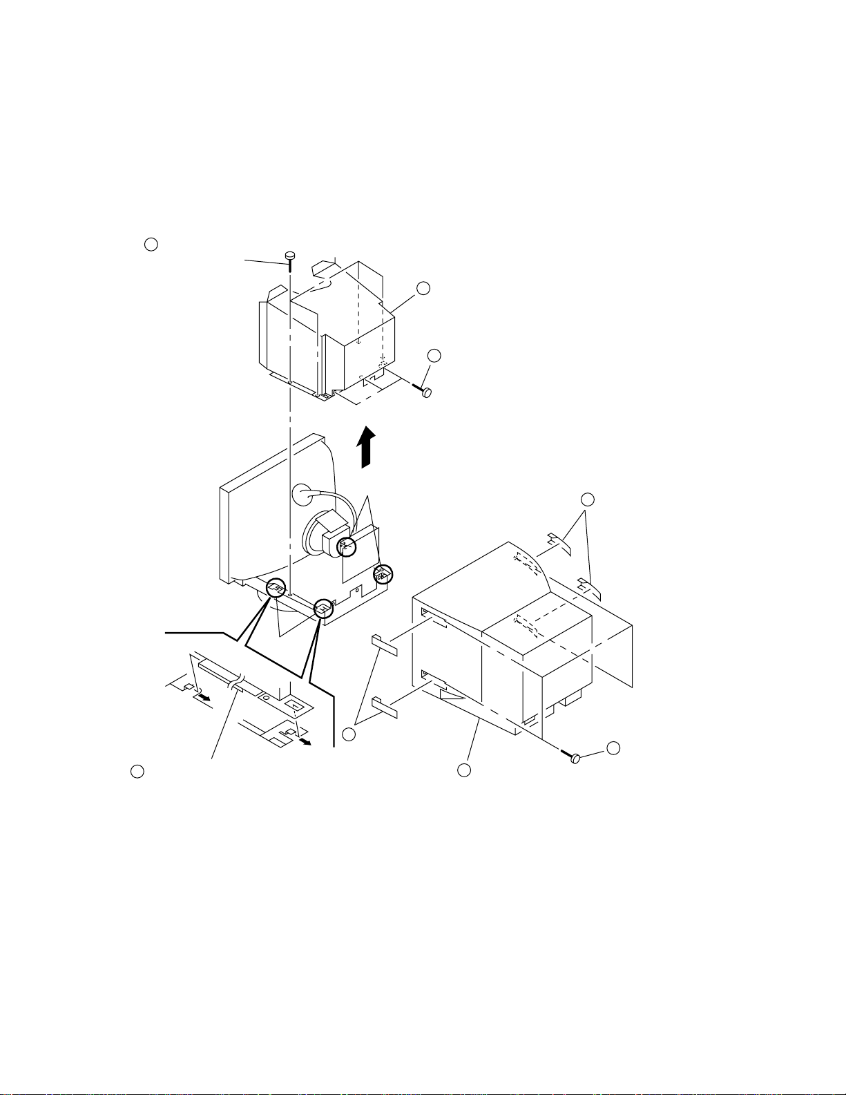
2-1. CABINET AND EMI SHIELD REMOVAL
5
Four screws
(+BVTT 3 x 8)
SECTION 2
DISASSEMBLY
8
EMI shield
6
Three screws
(+BVTT 3 x 8)
Claw
Claw
1
Two screw covers
(UR and LR)
7
Release from four claws after slide EMI shield
to direction of arrows.
4
Cabinet
2
Two screw covers
(UL and LL)
3
Four screws
(+BVTP 4 x 16)
2-1
Page 15

2-2. A AND D BOARDS REMOVAL
6550-23N/23S/33N/63N/63S/73N
5
A board
7
Four screws
(Washer head +P 3 x 8)
6
Three screws
(+BVTT 3 x 12)
2-3. SERVICE POSITION
CN601
GND
8
D board
GND
4
2
Cable stopper
Cable holder
1
3
Cable cover
Screw
(+BVTT 3 x 8)
A board
1
3
(Note) The electric potential of heat sink of IC401 is not GND.
So please do not touch it absolutely to the base chassis
D board
2
and etc., which make an ultimate cause of the bad movement or break.
2-2
Page 16

6550-23N/23S/33N/63N/63S/73N
2-4. PICTURE TUBE REMOVAL
11
Degaussing coil assembly
13
Neck assembly
14
Deflection yoke
9
Four screws
(Tapping screw 5)
1
Anode cap
CN2
2
A board
3
12
Two extention coils
4
CN303
2 pin
8 pin
CN601
GND
15
Two degaussing coil holders
Two claws
7
Screw
(+BVTT 4 x 8)
5
Stand assembly
6
Two screws
(+BVTP 4 x 16)
8
Base assembly
Two screws
(+BVTT 4 x 8)
16
Two degaussing coil holder
Cushion
10
Picture tube
Bezel assembly
• REMOVAL OF ANODE-CAP
NOTE: Short circuit the anode of the picture tube and the anode cap to the metal chassis, CRT shield or carbon painted on the CRT,
• REMOVING PROCEDURES
1 Turn up one side of the rubber cap in
• HOW TO HANDLE AN ANODE-CAP
1
2 Don’t press the rubber hardly not to damege inside of anode-caps!
3 Don’t turn the foot of rubber over hardly!
after removing the anode.
b
a
2 Using a thumb pull up the rubber cap
the direction indicated by the arrow a.
Don’t scratch the surface of anode-caps with shartp shaped material!
A material fitting called as shatter-hook terminal is built in the
rubber.
The shatter-hook terminal will stick out or damage the rubber.
firmly in the direction indicated by the
arrow b.
c
Anode Button
3 When one side of the rubber cap is
separated from the anode button, the
anode-cap can be removed by turning
up the rubber cap and pulling up it in
the direction of the arrow c.
2-3
Page 17

6550-23N/23S/33N/63N/63S/73N
MEMO
○○○○○○○○○○○○○○○○○○○○○○○○○○○○○○○○○○○○○○○○○○○○○○○○○○○○○○○○○○○○○○
○○○○○○○○○○○○○○○○○○○○○○○○○○○○○○○○○○○○○○○○○○○○○○○○○○○○○○○○○○○○○○
○○○○○○○○○○○○○○○○○○○○○○○○○○○○○○○○○○○○○○○○○○○○○○○○○○○○○○○○○○○○○○
○○○○○○○○○○○○○○○○○○○○○○○○○○○○○○○○○○○○○○○○○○○○○○○○○○○○○○○○○○○○○○
○○○○○○○○○○○○○○○○○○○○○○○○○○○○○○○○○○○○○○○○○○○○○○○○○○○○○○○○○○○○○○
○○○○○○○○○○○○○○○○○○○○○○○○○○○○○○○○○○○○○○○○○○○○○○○○○○○○○○○○○○○○○○
○○○○○○○○○○○○○○○○○○○○○○○○○○○○○○○○○○○○○○○○○○○○○○○○○○○○○○○○○○○○○○
○○○○○○○○○○○○○○○○○○○○○○○○○○○○○○○○○○○○○○○○○○○○○○○○○○○○○○○○○○○○○○
○○○○○○○○○○○○○○○○○○○○○○○○○○○○○○○○○○○○○○○○○○○○○○○○○○○○○○○○○○○○○○
○○○○○○○○○○○○○○○○○○○○○○○○○○○○○○○○○○○○○○○○○○○○○○○○○○○○○○○○○○○○○○
○○○○○○○○○○○○○○○○○○○○○○○○○○○○○○○○○○○○○○○○○○○○○○○○○○○○○○○○○○○○○○
○○○○○○○○○○○○○○○○○○○○○○○○○○○○○○○○○○○○○○○○○○○○○○○○○○○○○○○○○○○○○○
○○○○○○○○○○○○○○○○○○○○○○○○○○○○○○○○○○○○○○○○○○○○○○○○○○○○○○○○○○○○○○
○○○○○○○○○○○○○○○○○○○○○○○○○○○○○○○○○○○○○○○○○○○○○○○○○○○○○○○○○○○○○○
○○○○○○○○○○○○○○○○○○○○○○○○○○○○○○○○○○○○○○○○○○○○○○○○○○○○○○○○○○○○○○
○○○○○○○○○○○○○○○○○○○○○○○○○○○○○○○○○○○○○○○○○○○○○○○○○○○○○○○○○○○○○○
○○○○○○○○○○○○○○○○○○○○○○○○○○○○○○○○○○○○○○○○○○○○○○○○○○○○○○○○○○○○○○
○○○○○○○○○○○○○○○○○○○○○○○○○○○○○○○○○○○○○○○○○○○○○○○○○○○○○○○○○○○○○○
○○○○○○○○○○○○○○○○○○○○○○○○○○○○○○○○○○○○○○○○○○○○○○○○○○○○○○○○○○○○○○
○○○○○○○○○○○○○○○○○○○○○○○○○○○○○○○○○○○○○○○○○○○○○○○○○○○○○○○○○○○○○○
○○○○○○○○○○○○○○○○○○○○○○○○○○○○○○○○○○○○○○○○○○○○○○○○○○○○○○○○○○○○○○
○○○○○○○○○○○○○○○○○○○○○○○○○○○○○○○○○○○○○○○○○○○○○○○○○○○○○○○○○○○○○○
○○○○○○○○○○○○○○○○○○○○○○○○○○○○○○○○○○○○○○○○○○○○○○○○○○○○○○○○○○○○○○
○○○○○○○○○○○○○○○○○○○○○○○○○○○○○○○○○○○○○○○○○○○○○○○○○○○○○○○○○○○○○○
○○○○○○○○○○○○○○○○○○○○○○○○○○○○○○○○○○○○○○○○○○○○○○○○○○○○○○○○○○○○○○
○○○○○○○○○○○○○○○○○○○○○○○○○○○○○○○○○○○○○○○○○○○○○○○○○○○○○○○○○○○○○○
○○○○○○○○○○○○○○○○○○○○○○○○○○○○○○○○○○○○○○○○○○○○○○○○○○○○○○○○○○○○○○
○○○○○○○○○○○○○○○○○○○○○○○○○○○○○○○○○○○○○○○○○○○○○○○○○○○○○○○○○○○○○○
○○○○○○○○○○○○○○○○○○○○○○○○○○○○○○○○○○○○○○○○○○○○○○○○○○○○○○○○○○○○○○
○○○○○○○○○○○○○○○○○○○○○○○○○○○○○○○○○○○○○○○○○○○○○○○○○○○○○○○○○○○○○○
2-4
Page 18

6550-23N/23S/33N/63N/63S/73N
SAFETY RELATED ADJUSTMENT
SECTION 3
When replacing or repairing the shown below table, the
following operational checks must be performed as a
safety precaution against X-rays emissions from the unit.
Part Replaced ([)
RV501HV ADJ
Part Replaced (])
HV Regulator
Circuit Check
D board IC501, C532, C534,
C539, C553, C554,
C555, C556, C558,
C561, R540, R541,
R542, R544, R564,
R567, R568, RV501,
T501 (FBT)
HV Protector
Circuit Check
D board IC607, IC901, D515,
D517, C540, C542,
C544, R510, R543
R547, R549, R552,
R595,
T501 (FBT)
Beam Current
Protector Circuit
Check
D board IC605, IC607, IC901,
C535, C541, R545,
R546, R548, R550,
R596, R934,
T501 (FBT)
Confirm one minute later turning on the power.
*
• HV Protector Circuit Check
Using an external DC Power Supply, apply the voltage
shown below between cathode of D517 on D board and
GND, and confirm that the HV HOLD DOWN circuite
works. (TV Rester disappears)
Standard voltage : 35.80
+0.00
-0.10
V DC
Check Condition
• Input voltage : 120 ± 2 V AC
• Input signal : Cross hatch (White lines on Black
back ground) at 68.7kHz / 85Hz
(Mode 7)
• Beam control : CONT : 0 (min), BRT : 0 (min)
• Beam Current Protector Check
An ammeter in series between FBT pin !] on D board
and GND, then, decrease gradually the resistance of the
variable resistor from maximum to minimum, and confirm that the Beam Current Protector Circuite works
(TV Rester disappears). The current must be within the
range shown below.
• Standard current : 1.55
+0.00
-0.10
mA
Check Condition
• Input voltage : 120 ± 2 V AC
• Input signal : Cross hatch (Black lines on white) at
31.5kHz / 60Hz (Mode 1)
• Beam control : CONT : 0 (min), BRT : 0 (min)
• B+ Voltage Check
Standard voltage : 179.0 ± 3.0 V DC
Check Condition
• Input voltage : 120 V AC
Note : Use NF power supply or make sure that
distortion factor is 3% or less.
• Input signal : Cross hatch (White lines on black) at
68.7 kHz / 85Hz (Mode 7)
• Beam control : CONT : 255 (max), BRT : 255 (max)
3-1
Page 19

SECTION 4
6550-23N/23S/33N/63N/63S/73N
ADJUSTMENTS
Connect the communication cable of the computer to the connector located on the D board on the monitor. Run the service software
and then follow the instruction.
IBM AT Computer
as a Jig
1-690-391-21
1
D-sub
(9 Pin [female])
*The parts above ( ) are necessary for DAS adjustment.
mini Din
(8Pin)
1
A-1500-819-A
2
Interface Unit
3
• Landing Rough Adjustment
1. Enter the full white signal. (or the full black dots signal)
2. Set the contrast to “CONT”=MAX.
3. Make the screen monogreen.
Note: Off the outputs from R ch and B ch of SG.
4. Reverse the DY, and adjust coarsely the purity magnet so
that a green raster positions in the center of screen.
5. Moving the DY forward, adjust so that an entire screen becomes monogreen.
6. Adjust the tilt of DY, and fix lightly with a clamp.
Note: "TILT" shall be set at 0
• Landing Fine Adjustment
1. Put the set inside the Helmholtz coil.
2. Input the single green signal.
3. Demagnetize the CRT surface with the hand degausser , and
perform auto degaussing.
4. Attach the wobbling coil to the designated part of the CRT
neck.
5. Attach the sensor of the landing adjustment unit on the CRT
surface.
3-702-691-01
3
Connector Attachment
To BUS CONNECTOR
4 Pin
4 Pin 4 Pin
8. Adjust each top and bottom pins by two wedges and then not
swing DY neck right and left. Adjust H. Trap to become
horizontal trapezoid(c = d).
(When fixing DY with wedges, insert wedges completely so
that the DY does not shake.)
a
cd
b
“a” and “b” must be equal, and
“c” and “d” must be equal.
Signal : Inverted crosshatch (Make the monogreen)
B
R
R
A
B
A1
“A” and “B”,
“A1” and “B1”
B
R
R
B
B
B1
must be equal.
<How to drive in wedges>
Purity Magnet <<Zero Position>>
Purity magnet position
L/D control specification
± 5 ± 7 ± 5
± 5 ± 7 ± 5
± 5 ± 7 ± 5
6. Adjust the DY position and purity, and the DY tilt.
7. Fasten DY with screw.
Note: Torque 22 ±2kgcm (2.2 ± 0.2 Nm)
Perform auto degaussing.
9. If the L/D is not within the standards adjust purity magnet
and in front and behind of DY to satisfy L/D adjustment
standards. If the corner is not within the standards, adjust
disc magnet to satisfy L/D adjustment standards.
Note:
(1) When necessary to paste magnets more than 2 pieces, be
careful that the convergence and the distortion would be alterable.
(2) Paste within 80 to 120 mm from the DY on the diagonal line
of the magnet.
10. If using the magnet, be sure to demagnetize with the degausser and check.
11. Remove the sensor and wobbling coil.
12. Check that the DY is not tilting.
4-1
Page 20

6550-23N/23S/33N/63N/63S/73N
A
312 mm
B
MODE All mode
234 mm
a 1.8 mm
b 1.8 mm
a
B
A
b
• Convergence Rough Adjustment
1. Enter the white crosshatch signal (white lines on black).
2. Adjust roughly the horizontal and vertical convergence at
four-pole magnet.
3. Adjust roughly HMC and VMC at six-pole magnet.
• Convergence Adjustment
Static convergence
1. Receive the crosshatch of R and B.
2. Recieve H. STAT and V. STAT by 4 pole magnet.
3. Recieve the white crosshatch signal.
4. Recieve HMC and VMC by 6 pole magnet.
5. Recieve the crosshatch of R and B.
Note: Adjust H. STAT and V. STAT in the beggining by 4 pole
magnet not adjuust them by register immediately.
6. Insert to TLH correction board and correct H. TILT.
7. Correct XCV by XCV core.
8. Correct V. TILT bu TLV-VR.
9. Adjust Y cross by YCH-VR.
10. Correct to get the most suitable convergence pattern.
When necessary, adjust above mentioned from step 1 to step
10 reiterate.
11. Paint lock TLH corection board, neck assy 4 and 6 pole
magnet.
Purity Mg
4-pole Mg
6-pole Mg
XCV
• Convergence Specification
B
A
MODE All mode
0.20 mm
A
0.24 mm
B
• White Balance Adjustment Specification
(1) 9300K
x = 0.283 ± 0.005
y = 0.298 ± 0.005
(2) 5000K
x = 0.346 ± 0.005
y = 0.359 ± 0.005
• Vertical and Horizontal Position and Size
Specification
XCV YCH
TLV
B
R
R
B
B
R
RB
TLH
R
B B
R
<<Neck Assy's Zero Position>>
Purity
4 Pole 6 Pole
TLH
YCH
TLV
H-Trap
• Focus adjustment
Adjust the focus volume 1 and 2 for the optimum focus.
Standard: HMC, VMC ± 0.1 mm (In the center of screen)
FBT
Focus volume 1 (V)
Focus volume 2 (H)
4-2
Page 21

5-1. BLOCK DIAGRAMS
5
4
3
2
1
SIGNAL IN
(PIG-TAIL)
15
10
14
9
13
8
12
7
11
6
HD15
CN313
B GND 1
BLUE 1
G GND 1
GREEN
R GND 1
RED 1
GND
VD 1
HD 1
CN310
NC
DDC SCL
DDC SDA
HOST GND 1
SECTION 5
DIAGRAMS
1
2
3
4
5
6
7
8
9
1
2
3
4
IC006 H BUFF
8
9
4
CN305
+180V1
IC001
RGB DRIVE, OSD MIX
7
B IN
9
G IN
11
R IN
10
10
5
6
SYNC IN
B OUT
G OUT
R OUT
B BKG
G BKG
27
24
20
3
4
5R BKG
IC002
RGB OUT
11
B IN
9
G IN
8
R IN
RGB CUT - OFF CONT
5
B IN
4
G IN
3
R IN
B OUT
G OUT
R OUT
IC004
B OUT
G OUT
R OUT
J001
1
3
5
9
8
7
9
KB
8
KG
7
KR
G2
4
H
10
2
3
4
5
6
7
8
9
NC
+80V
GND
H1
+12V
GND
+5V
STBY +5V
D
TO
D BOARD
CN502
A
TO
D BOARD
CN902
1 - 4
B
TO
D BOARD
CN903
C
TO
D BOARD
CN902
5 - 0
CN311
NC
HOST GND 1
DDC SDA
DDC SCL
NC
CN309
C BLK
INPUT SELECT
BP CLP
C SYNC
VS OUT
GND
H SYNC
SYNC DET
CN306
IIC SDA
GND
IIC SCL
HOST GND 2
HR TRC
VR TRC
1
2
3
4
5
1
2
3
4
5
6
7
8
6
5
4
3
2
1
INV.
Q006
1
2
18
12
30
7
8
10
5
SDA
SCL
BLK
CLAMP
C SYNC
SDA
SCL
V FLB
H FLB
IC003 OSD
OSD BLK
R OSD
G OSD
6G2
13B OSD
14G OSD
15 R OSD
17 OSD BLK
12
15
14
13 B SOD
IC005
G2 CUT - OFF CONT
5
+
-
6
7
SPOT KILLER
Q001
A
(VIDEO)
CN301
1
1.2KV
E
TO
D BOARD
CN510
5-1 5-2
B-SS9180<U/C>-BD1-24
Page 22

TO
A BOARD
CN311
TO
A BOARD
CN306
+12V
15
KEY SCAN
LED RED
48
47
LED GRN
38
RDI
39
TDO
C BLK
46
22
CLP
28
CSI
20
VSI1
30
HSI1
34
DDC SCL
35
DDC SDA
33
HOST GND
37
SDA
36
SCL
25
PD3
VSO
26
54
RESET
21
VSI2
7
DEGAUSS
HEATER SW
24
6
REMOTE ON/OFF
IC901 CPU
44
OSC OUT
OSC IN
THERMAL
H CENT
ROTATION
X901
24MHz
45
17
TH501
HSO
27 26
23
LOCK
32
HFB
4
19
VFB
18
HV
49
S0
53
S4
16
ABL
2
STBY
3
X902
S901-S906,S908
D912
CN901
1
D GND
2
+5V
RXD
3
4
TXD
CN903
1
C BLANK
2
INPUT SELECT
BP CLAMP
TO
A BOARD
B
CN309
CN902
1
DDC SCL
2
A
C
DDC SDA
HOST GND 1
NC
11C DATA
GND
11C CLK
HOST GND 2
HRTRC
VRTRC
3
4
5
6
7
8
9
10
STBY
+5V
5
8
5
6
C SYNC
V SYNC
GND
H SYNC
SYNC DET
IC904 RESET
OUT
VCC
IC905 EEPROM
VCC
SDA
WC
SCL
3
4
5
6
7
8
4
7
29
X5
3
SDA
4
SCL
H IN
25
V IN
IC902 DEF CONTR0L
V DF
E/W
H OUT
H FLY
V SAW
V SIN
V DIV
LOCK
BUFF
Q505
7 3
H DRIVE
Q501,502
IC401 V OUT
-IN
+IN
DF AMP
Q504
OUT
D517
12
9
H AMP
17
Q903
14
8 1 5
10
27
2
FB
+
T503
DFT
64
82
H DRIVE
OUT
Q511
H BLK
BUFF
Q508
SYNC LOCK
Q522, 524
BUFF
Q506
RY500
L509
HLC
T504
HDT
H CENT
CONT
Q518
RELAY
DRIVE
Q519
S-CAP CHANGE
Q512-516
64
H OUT
81
Q507
S0-S4
L511
S0-S4
S4
T505
HST
52
31
BUFF
Q521
IC503
H CENT AMP
-IN
+IN
1 3
IC502 ROTATION DRIVE
REF V
+IN
1
+IN
2 4
OUT
H REG
Q520
42
5
BUFF
3
23
2
8
4
H CENT
5
2
OUT
L503
+
24 22
IC501 PWM CONTROL
REF
HV REG OUT
Q510
CHOPPER
Q503
D515
+
20
+
19
-
18
+
AMP
13
14
+
12
T501 FBT
2
1
7
6
D522
D523
HV
13
16
FV1
15
14
FV2
11
12
TO
PICTURE TUBE
RV501
HV
ADJ
FOCUS
FOCUS
ABL
CN501
1
H DY+
2
H DY+
3
H DY-
4
H DY-
5
V DY-
6
V DY+
CN510
1.2kV1
H -DY
V-DY
TO
A BOARD
E
CN301
TO
A BOARD
CN305
IC702
H FLY
BUFF
Q525
+12V
RY601
RELAY
DRIVE
CN601
1
DGC
D
DGC 2
DGC 1
AC IN
CN602
THP600A
THP600
CN502
+180V
NC
+80V
GND
H1
+12V
GND
+5V
SRBY +5V
2
N
3
TH601
CN600
F601
L21
G
N
2
1
1
2
3
4
5
6
7
8
9
34
+180V
+80V
+12V
+5V-2
STBY +5V
HEATER OUT
4
Q601
D612
D613
REG SW
+5V REG
I O
I O
IC605
+12V REG
IC607
Q603
I O
IC608
+5V REG
+180V
+80V
+15V
STBY +5V
-15V
+12V
+5V-2
LF602
S602
LFT
TH600
IC602
CTL
1
OUT
VCC
2
5
VADJ
D601
AC RECT
Q605
T601
SRT
9
IC601
SW REG CONT
1
V IN
D609
SW
DRIVER
14
OOB
I SENSE
9
VCTL
8
IREF
V AUX
DEM
11
GND
IC603
5
1
4
2
DS
4
5
7
6
13
POWER
SWITCHING
Q602
OVP/OCP
Q604
3 1
IC604 ERROR AMP
8
7
5
D620
2
3
D605
D619
D611
10
D617
11
12
D618
13
D614
14
D622
15
D615
16
17
D616
18
D CONVERGENCE OUT
11
STBY
+IN B
3
+IN A
IC701 CONVERGENCE CONTROL
16
SDA
SCL
17
14
HD IN
VS IN
2
V POS IN
3
V REF OUT
5
H CONV OUT
V CONV OUT
H STATIC OUT
V STATIC OUT
IC703
S CONVERGENCE OUT
4 3
+IN A
+IN B
OUT B
OUT A
-IN A
I OUT A
OUT A
-IN B
I OUT B
OUT B
-IN B
-IN A
1
2
6
54
1
2
3
6
8
8
9
1
2
76
9
8
4
5
6
7
8
9
10
CN701
ROTATION+
ROTATION-
CY1+
CY1CY2+
CY2CY3+
CY3CY4+
CY4-
ROTATION
CY-DY
D
CONVERGENCE CONTROL,
DEFLECTION, CPU,
POWER SUPPLY
B-SS9180<U/C>-BD2-24
5-3
5-4
Page 23

5-2. CIRCUIT BOARDS LOCATION
D
5-3. SCHEMATIC DIAGRAMS AND PRINTED
WIRING BOARDS
Note:
• All capacitors are in µF unless otherwise noted. (pF: µµF)
Capacitors without voltage indication are all 50 V.
• Indication of resistance, which does not have one for rating
electrical power, is as follows.
Pitch: 5 mm
Rating electrical power 1/4 W (CHIP : 1/10 W)
• All resistors are in ohms.
f : nonflammable resistor.
•
• F : fusible resistor.
¢ : internal component.
•
p : panel designation, and adjustment for repair.
A
•
• All variable and adjustable resistors have characteristic curve B,
unless otherwise noted.
e : earth-ground.
•
• E : earth-chassis.
• All voltages are in V.
• Readings are taken with a 10 MΩ digital multimeter.
• Readings are taken with a color-bar signal input.
• Voltage variations may be noted due to normal production
tolerances.
•
• Circled numbers are waveform references.
•
• S : B – bus.
• The components identified by
• When replacing components identified by
• When replacing the part in below table, be sure to perform the
: Can not be measured.
*
s : B + bus.
have been carefully factory-selected for each set in order to
satisfy regulations regarding X-ray radiation.
Should replacement be required, replace only with the value
originally used.
necessary adjustments indicated. (See page 3-1)
related adjustment.
[ in this basic schematic diagram
], make the
Part Replaced ([)
RV501HV ADJ
Part Replaced (])
HV Regulator
Circuit Check
D board IC501, C532, C534,
C539, C553, C554,
C555, C556, C558,
C561, R540, R541,
R542, R544, R564,
R567, R568, RV501,
T501 (FBT)
HV Protector
Circuit Check
D board IC607, IC901, D515,
D517, C540, C542,
C544, R510, R543
R547, R549, R552,
R595,
T501 (FBT)
• Divided circuit diagram
One sheet of D board circuit diagram is divided into four
sheets, each having the code D-a to D-d . For example, the
destination ab1 on the D-a sheet is connected to ab1 on the
D-b sheet.
1
a
b
Ref. No.
Circuit diagram division code
Terminal name of semiconductors in silk screen
printed circuit ( )
Device Printed symbol Terminal name
Transistor
1
Transistor
2
3
Diode
4
Diode
Diode
5
Diode
6
Diode
7
8
Diode
Diode
9
Diode
0
Diode
!¡
Diode
!™
Transistor
!£
(FET)
Transistor
!¢
(FET)
Transistor
!∞
(FET)
Transistor
!§
Discrete semiconductot
–
(Chip semiconductors that are not actually used are included.)
Note: The components identified by shading and mark
! are critical for safety. Replace only with part
number specified.
*
Collector
Base
Collector
Base
Cathode
Cathode
Anode
Cathode
Anode
Common
Anode
Common
Anode Cathode
Common
Anode
Common
Anode Anode
Common
Cathode
Common
Cathode
Anode
Anode
Cathode
Drain
Drain
Emitter
Emitter
Anode
(NC)
(NC)
Cathode
Anode
Cathode
Cathode
Cathode
Anode
Anode
Source
Gate
Source
Gate
Source
Drain
Gate
Emitter
Collector
Base
Circuit
D
G
D
S
D
G
S
S
D
G
G
S
Ver.1.6
5-5
Beam Current
Protector Circuit
Check
D board IC605, IC607, IC901,
C535, C541, R545,
R546, R548, R550,
R596, R934,
T501 (FBT)
Note: Les composants identifiés par un tramé et une
marque ! sont critiques pour la sécurité. Ne les
remplacer que par une pièce portant le numéro
spécifié.
5-6
Page 24

(1) Schematic Diagram of D (a-d) Boards
123456789101112
A
D
G
H
B
C
E
KEY SCAN
ab1
ab2
C929
STBY 5V
0.001
B:CHIP
R705
4.7k
R719
15k
:RN-CP
OUTA
R940
2.7k
:RN-CP
R943
470
R944
560
:CHIP
R945
1k
:CHIP
R946
1.5k
:CHIP
R947
3.3k
:CHIP
R755
4.7k
:RN-CP
R706
R753
4.7k
15k
:RN-CP
:RN-CP
C725
0.01
B:CHIP
3.8 3.8 3.8 0.2
INA+
VEE
INB+
INA-
R727
15k
:RN-CP
B:CHIP
R747
2.2
:CHIP
INB-
C733
330p
OUTB
I OUTB
R711
0.56
1W
R729
2.2
1W
:RS
VCC
R712
33
1W
:RS
C711
0.1
:PT
C716
0.033
25V
B:CHIP
C718
0.033
25V
B:CHIP
C702
4.7
R707
R709
2.2k
2.2k
:RN-CP
:RN-CP
C706
R731
0
68p
:CHIP
CH:CHIP
R728
100
1W
:RS
R730
12
1W
:RS
2.5 2.5 2.5 2.5-0.2
1 2 3 4 5 6 7 8 9 10 11 12
OUTB
INB-
RESET
BRIGHT-
BRIGHT+
MENU
CONT-
CONT+
CN701
10P
YEL
:S-MICRO
10
CY-DY
ROTATION
F
CY4CY4+
CY3CY3+
CY2CY2+
CY1-
CY1+
ROTATIONROTATION+
9
8
7
6
5
4
3
2
1
R718
100
1W
:RS
R724
18
1W
C708
0.1
:PT
OUT
C549
0.068
:PT
-15V
IN-
1.1
IN+
R560
15k
:RN-CP
C547
12345
1.0
R559
2.7k
:RN-CP
1.0
STBY5V
R558
6.8k
:RN-CP
R562
18k
R566
22
1W
:RS
ROTATION DRIVE
:RN
R563
1.5
:FPRD
IC502
LA6500-FA
15V
-0.6
C513
10
S901
S903
S904
S905
S906
S908
:RN-CP
R717
2.2
1W
:RS
C729
330p
B:CHIP
R745
2.2
:CHIP
1 2 3 4 5 6 7 8 9 10
I OUTA
1 3
I
CONVERGENCE
4.9
123456789
4.9
5.0
4.9
5.0
5.0
5.0
5.0
5.0
V.SIN
C707
68p
CH:CHIP
R735
2.2k
:RN-CP
INB+
IC701
CXA8070AP
CONTROL
A_GND
D_GND
V_SIN
SCL
VPOSIN
SDL
V_DF
D_VCC
VREF OUT
HD.IN
H_CONVOUT
V_REFIN
V.CONVOUT
H-SAW_CAP
H_STATICOUT
H-AGC_CAP
V_STATICOUT
A_VCC
R710
R708
2.2k
2.2k
:RN-CP
:RN-CP
R733
0
:CHIP
C723
0.01
B:CHIP
R737
2.2k
:RN-CP
INA+
INA-
D CONVERGENCE OUTS CONVERGENCE OUT
ab6
ab7
ab8
ab9
ac1
ab10
4.7
4.2
C714
390p
CH:CHIP
3.7
4.9
4.9
10 11 12 13 14 15 16 17 18
C705
0.1
:PT
D935
HZS5.1N
D704
1SS119
R704
8.2k :RN-CP
C701
0.1
25V
B:CHIP
C704
220p
CH:CHIP
C703
0.22
:MPS
C715
470
16V
12V
C712
0.1
:PT
C713
2200
10V
5V-2
R703
270
1/4W
JW901
JW(5)
ab11
ab12
R743
0.47
R741
0.47
C710C709
470
25V
ab13
15V
STK391-110LA6510
R716
33
1W
:RS
OUTA
42
IC702IC703
VEE
R713
0.68
1W
VCC
R739
10k
:CHIP
3.2
STBY
-15V
470
25V
:FPRD
:FPRD
ab14
-a
D
(CONVERGENCE CONTROL)
B-SS9180<U/C>-D..-P1-24
• Divided circuit diagram
One sheet of D board circuit diagram is divided into four
sheets, each having the code D-a to D-d . For example, the
destination ab1 on the D-a sheet is connected to ab1 on the
D-b sheet.
1
a
b
Ref. No.
Circuit diagram division code
5-7
Schematic diagram
-a board
D
ll
l
ll
•D - a BOARD WAVEFORMS
1
0.1 Vp-p (V)
23
0.16 Vp-p (V)
5-8
2.4Vp-p (V)
4
2.0 Vp-p (V)
Page 25

1234567891011 1312
A
D
B
C
E
STBY
D901
5V
R905
0
:CHIP
R921
0 :CHIP
R912
1k :CHIP
R913
100
:CHIP
R914
100
:CHIP
R923
0 :CHIP
H FLY
CBLANK
1k :CHIP
R904
1k
:CHIP
R918
1k
:CHIP
D507
HZS5.1N
R935
100
:CHIP
R938
100
:CHIP
:CHIP
ab1
ab2
ab6
ab13
ab7
ab9
ab8
ab10
ab11
C901
R907
0.47
100
16V
1/2W
B:CHIP
C903
0.01
B:CHIP
C902
470
16V
C938
220
16V
C906
1.0
:MPS
C934
100p
CH:CHIP
D937
HZS5.6NB2
R915
4.7k
:CHIP
IIC DATA
IIC CLK
C905
0.068
:PT
V SAW
E/W
V.SIN
C913
0.1
:PT
ab12
F
V SAW
E/W
V.DF
IIC CLK
123456789101112131415
D.GND
D VCC
4.8
LOCK
4.2
4.0
6.0
4.9
4.2
4.9
6.1
4.7 5.2
0.7
V-REF
H BLK
V.IN
SDA
V.DIV
SCL
H.IN
V.GND
H.PH.FI
V.OSC
AFC1
V.AGC
1
V.SAW
2
E/W
VCO.FI
V.SIN
R.F/V
H.AGC
DELAY CAP
3
V.DF
AFC2
H.DF
4
H.OUT
H.FLY
0.4
H.GND
IC902
CXA8071CP
DEF CONTROL
C937
0.47
16V
B:CHIP
X5
REF
9V
VCC
B:CHIP
C936
100p
CH:CHIP
X902
0.4
V-USYNC
5.04.5
4.7
H-USYNC
3.6
4.9
V-REF
10.2
2.4
9.4
C916
22
C917
0.01
B:CHIP
R933
1k
16 17 18 19 20 21 22 23 24 25 26 27 28 29 30
C925
0.01
C918
10
R504
0.47
:FPRD
Q501
2SC2412
H DRIVE
5.5
12V
2SA1037
H DRIVE
:RN-CP
D903
RB441QT
0.4
C926
470
16V
C935
0.47
16V
B:CHIP
R594
220
:CHIP
5.5
5.5
Q502
R931
2.2k
5.5
R929
4.7k
:CHIP
C922
1.0
C920
0.01
B:CHIP
Q903
2SC2412
H AMP
V-REF
R951
:CHIP
D920
RB501V-40
C923
470p
CH:CHIP
C924
C921
22
470
16V
D925
MA111
D922
1.2k
:CHIP
D927
MA111
D923
0
D926
MA111
D924
MA111
LOCK
100
H-USYNC
ABL
ABL
THERMAL
R922
10k
:CHIP
KEY SCAN
R934
10k
C927
0.01
B:CHIP
V-USYNC
C930
0.01
:PT
12V
C928
0.01
B:CHIP
R932
15k
:CHIP
V FLY
5.0
2.7
ROTATION
1.9
H.CENT
D921
MA111
5.0
0
DEGAUSS
D936
HZS5.6NB2
D902
HZU5.6B2TRF
0.8
D938
HZU5.6B2TRF
4.8
4.8
D918
HZU5.6B2TRF
D919
MA111
HV
3.6
V FLY
4.2
V-SYNC
5.0
0
4.8
5.0
HEATER
10
H-USYNC
4.7
CSYNC
0.5
12 13
H CENT
12345678910111213141516171819202122232425262728
DA0
DA1
5
DA2
6
DA3
DA4
DA5
DA6
DA7
DA8
VSS2
7
VDD2
8
PB7
OSCOUT
PB6
CLKOUT
PB5
PB4
4.0
PB3
2.8
PB2
PB1
VFB
9
VSI1
VSI2
CLP
DDCSDA
ITA
DDCSCL
PD4
PD3
14
VSO
HSO
11
CSI
IC901
CXD9529S
CPU
TEST
RESET
PA0
4.9
PA1
0.4
PA2
4.9
PA3
0.4
PA4
0.4
PA5
PA6
CBLK
OSCIN
2.2
2.4
TDO
RDI
SDA
SCL
PC1
HFB
VDD
HSI1
VSS
IR
NC
NC
NC
IIC CLK
IIC DATAIIC DATA
4.8
HZU5.6B2TRF
HZU5.6B2TRF
LED RED
4.4
LED GREEN
1.0
CBLANK
C914
15p CH:CHIP
X901
24MHz
C915
15p
CH:CHIP
5.0
TXD
5.0
RXD
4.2
IIC DATA
4.6
IIC CLK
1.6
DDC DATA
4.4
DDC CLKLOCK
5.0
HOST GND
0.7
C909
1000
10V
4.6
C908
29 30 31 32 33 34 35 36 37 38 39 40 41 42 43 44 45 46 47 48 49 50 51 52 53 54 55 56
0.01
B:CHIP
RESET
D904
D934
D933
HZS5.6NB2
D932
HZS5.6NB2
HZS5.6NB2
R920
:CHIP
HZU5.6B2TRF
FB904
STBY
:CHIP
D915
MA111
D931
1k
D930
D929
HZU5.6B2TRF
5V
:CHIP
R908
2.2k
:CHIP
D917
MA111
R909
2.2k
R927
:CHIP
S0
S1
S2
S3
S4
0
C910
4.7
:BP
STBY
5V
D912
SML16751WN
R911
820
R910
330
D928
HZU5.6B2TRF
R957
47 :CHIP
R958
47 :CHIP
IC904
PST9143NL
RESET
123
VCC
NC
SUB
GND
OUT
HV
4 5
4.8
IIC DATA
IIC CLK
R925
470k
:CHIP
C912
100
16V
RXD
TXD
R916
15k
:CHIP
D909
HZU5.6B2TRF
VSSSDA
5 6 7 8
4.1
4.7
D911
MA111
V FLY
CSYNC
BPCLAMP
D913
MA111
R917
15k
:CHIP
D906
MA111
ICC DATA
IIC CLK
D907
MA111
D910
HZU5.6B2TRF
1234
A0
A1
A2
SCLWCVCC
5.0
C911
0.01
1SS119
D908
MA111
DDC CLK
IC905
M24C08-MN6T
EEPROM
:PT
R906
:CHIP
D905
R901
JW(5)
10k
MA111
R903
R936
100
R924
100
:CHIP
R937
100
:CHIP
1
D GND
2
+5V
3
RXD
4
TXD
CN901
4P
WHT
:S-MICRO
1
DDCSCL
2
DDCSDA
3
HOST GND1
4
NC
5
IICDATA
6
GND
7
IICCLK
8
HOST GND2
9
HRTRC
10
VRTRC
CN902
10P
WHT
:S-MICRO
CN903
8P
WHT
:S-MICRO
1
CBLANK
2
INPUT SELECT
3
BPCLAMP
4
CSYNC
5
VSYNC
6
GND
7
HSYNC
8
SYNC DET
TO A BOARD
CN309
TO A BOARD
CN311
TO A BOARD
CN306
G
H
ab14
ROTATION
bc2
bc1
D
-b
bc3 bc4 bc5 bc6 bc7
(DEFLECTION,CPU)
• Divided circuit diagram
One sheet of D board circuit diagram is divided into four
sheets, each having the code D-a to D-d . For example, the
destination ab1 on the D-a sheet is connected to ab1 on the
D-b sheet.
1
a
b
Ref. No.
Circuit diagram division code
5-9
bc8
CH:CHIP
bc9
C931
470p
H BLK
HEATER
DEGAUSS
REMOTE ON/OFF
V-SYNC
D916D914
MA111MA111
H-SYNC
bd2
bd1
bd3 bc10 bc11 bc12 bc13 bc14
•D - b BOARD WAVEFORMS
1
2.6 Vp-p (V)
8
3.2 Vp-p (24NHz)
23
0.3 Vp-p (V)
1.0 Vp-p (V)
90
4.0 Vp-p (V)
5.0 Vp-p (V)
4
0.7 Vp-p (H)
!¡
5.0 Vp-p (H)
5-10
B-SS9180<U/C>-D..-P2-24
5
5.0 Vp-p (H)
!™
4.0 Vp-p (H)
6
5.0 Vp-p (H)
!£
5.0 Vp-p (H)
7
4.0 Vp-p (H)
!¢
4.6 Vp-p (H)
Page 26

1234567891011 141312
A
B
C
D
E
G
H
C545
R556
0.022
47k
B:CHIP
:RN-CP
C546
220p
CH:CHIP
C562
100
16V
:HT
123
4.2 4.2 4.5 5.6 8.2 6.7
B1 B2
CP1 CP2 CP3
RR R R R
R557
18k
:CHIP
12V
:RN
B3
R
R
SAW GEN2 NON AGC TYPE
C548
0.001
:PT
C576
47p
CH:CHIP
TO PICTURE TUBE
DP1 B4
4
B4
4.2
1 2 3 4 5 6 7
4.2 5.5 8.9 4.2 8.3 4.5 5.9
91k
1M
C550
100
16V
R552
56k
:RN
L507
10µH
ABL
R550
1.2k
:RN
C541
4.7
C552
0.01
B:CHIP
C563
470p
B:CHIP
R596
1.2k
C544
0.01
:PT
C582
:RN
C564
0.47
16V
B:CHIP
R541
1k
:RN
R545
47k
:RN-CP
R546
33k
:RN
R510
4.7k
:RN
R553
:RN-CP
C539
0.01
100V
R544R542
R548
1.2k
:RN
D517
HZT33-02
R549
62k
:RN
D
CN512
(DEFLECTION)
1P
:TUB
L513
10µH
8
R584
4.7k
:CHIP
-c
ABL
Q524
2SA1037
SYNC LOCK
5.5
HV
13
16
C532
0.22
100V
FV1
FOCUS(V)
15
14
SG501
FV2
FOCUS
HSS82
11
NX4404
12
bc2bc7bc11bc12bc10
E/W
R569
470
:RN-CP
C543
100p
CH:CHIP
C534
0.033
100V
:PT
(H)
D514
T501
:FBT
R554
150k
:RN-CP
IC501
µPC6757CS
PWM CONTROL
R551
33k
0.022
:RN-CP
B:CHIP
C551
0.01
B:CHIP
R597
R540
2.2M
200k
1k
:RN
RV501
100k
HV ADJ
C535
0.1
:PT
R595
R547
220k
220k
:RN
:RN
C542
10
50V
C540
10000p
630V
:PP
bc8bc9bc6bc14bc5bc4bc1ac1 bc13
IC401
TDA8177
V OUT
1 2 3 4 5 6 7
1.6 -14.2 1.60.3 14.1
-15V
C402
C401
0.47
1000
250V
:PT
D518
HZS10N
175.0
D516
D2L40
C518
4300p
1.8kV
L506
820µH
38.6
C410
0.47
F:CHIP
R402
330 1W :RS
R403
C574
0.01
250V
C521
100p
2kV
SL
12V
1
1SS119
2
R576
47k
S-CAP CHANGE
R519
56k
:RN
S3
25V
:HT
R401
1.0
V SAW
:FPRD
180V
7
R512
4.7
C507
0.19
400V
B
C575
33
200V
97.5
-0.5
R522
47
2SC5302
H OUT
C573
4.7
250V
R515
:FPRD
S4
2SJ516
Q507
C511
0.22
250V
:PP
1k
0.4
B:CHIP
R581
10k
S
FB506
1.1
97.4
Q520
H REG
FB504
1.1
D506
FMQ-G2FS
RY500
R578
39
2W
:RS
2SK3155
S-CAP CHANGE
C512
0.01
T504
:HDT
1
8
12V
T503
:DFT
7
D502
D3S4M
6
R518
L509
HLC
C583
0.1
:PT
56
4
3
2
1
2.2
3W
:RS
R517
2.2
3W
:RS
2
6
-0.2
R513
220
:RS
S
3
4
2W
C510
470p
500V
108V
B
cd1
C502
0.01
:PT
Q511
IRFU110
H DRIVE OUT
R508
D501
100
HZS12N
R509
-10.6
22k
5
cd2
23
15
:PT
C504
330p
500V
R532
2.2
:FPRD
B
C508
-15V
R590
22k
:RN
R565
330k
:RN
100
25V
:HT
R511
1
:FPRD
R589
4.7k
5.7
5.0
8
Q521
2SA1309A
BUFFER
7
8
R516
150
1/2W
:RN
L508
HLC
R591
1/2W
150
:RN
R592
150
1/2W
:RN
4
T505
HST
D512
1SS119
C517
0.01
cd3
D505
ERB91-02TP1
R577
33
3W
:RS
F
Q504
12V
2SC3941A
DF AMP
1.0
R507
C503
2.7k
0.01
:RN
B:CHIP
D510
ERA34-10TP1
C528
D520
0.01
C578
2kV
F
C505
47p
2kV
167.7
R506
330k
:RN
0.5
22p
2kV
SL
R
bc3
910 1112
12345
H DY+
H DY+
H DY-
H DY-
V DY-
R501
100
:CHIP
6
CN501
6P
V DY+
:DY
R502
180k
:RN-CP
C501
0.7
10
R503
10k
:RN-CP
Q505
2SA1309A
BUFFER
D521
ERA34-10TP1
C577
0.01
2kV
F
1
CN510
1.2KV
1P
TO A BOARD
CN301
R505
10k
:CHIP
0.9
-15V
ERA34-10TP1
25V
C406
0.0047
:PT
:RN-CP
R405
1.5
1.5
:RN
:RN
D525
HSS83
C522
0.0022
100V
:PT
D519
C514
0.82
250V
:PP
Q513Q514
2SK2098
37.9
R521
1k
:FPRD
0.4
C515
0.01
B:CHIP
C403
220
:HT
R408
10k
:CHIP
C405
0.047
B:CHIP
R404
5.6k
:RN-CP
C579
22p
2kV
SL
D524
HSS83
R585
1k
1/4W
R586
2.2k
RELAY DRIVE
11.9
C572
4.7
250V
R575
68
1/2W
:FPRD
L505
2.2mH
C516
0.3
250V
:PP
0.12 250V :PP
SS
R406
12k
HZS5.1N
DTC114TSA
C530
D401
D1NL40
R407
2.2k
:CHIP
D403
MA111
D402
HZS4.7N
C407
0.022
:PT
R582
56
L503
:FPRD
5mH
1
2
4
5 6
H BLK
D527
-90V
Q519
0.4
Q512
2SK3155
S-CAP CHANGE
R525
4.9
1k
:FPRD
R524
C520
56k
0.01
:RN
B:CHIP
S2
15V
V-REF
C404
1000
25V
:HT
R410
12k
:RN-CP
R409
5.6k
:RN-CP
H FLY
12V
10
9
R599
1k
0.2
L510
C580
3.3µH
0.01
13
:PT
97.3 96.3
97.2
R573
220k
D511
HZS5.6NB2
C523
0.12
250V
:PP
C531
0.068
250V
:PP
0
S
D404
RB501V-40
Q525
2SC3311A
H FLY BUFFER
12V
C569
0.2
0.1
:PT
0.7
R587
Q508
1k
2SC3311
H BLK BUFFER
R539
10
3W
:RS
R579
IC503
LA6500-FA
H CENT AMP
12345
R572
R570
47k
R571
33k
:RS
47.9
R580
2.0
15k
:CHIP
C568
0.047
400V
:PP
Q515
2SK3155
S-CAP CHANGE
38.0
R533
1k
0.4
:FPRD
R523
C536
56k
0.01
:RN
B:CHIP
S1
R538
10
3W
:RS
150k
1k
3W
12V
R529
10k
:FPRD
2.6
R500
0.47
C509
:FPRD
100p
500V
B
H BLK
C570
100
25V
:HT
C559
0.0047
:PT
2.6
Q518
2SC2610TZ
H CENT
CONTROL
C525
0.047
400V
STBY
5V
:PP
C538
R536
0.01
1k
B:CHIP
:FPRD
R535
56k
S S
:RN
4.9
S0
Q506
2SA1309A
BUFFER
2.0
L511
47µH
C529
0.047
400V
:PP
0
S-CAP CHANGE
R514
22k
:CHIP
C506
1
Q516
2SK3155
R537
56k
:RN
C560
0.36
250V
:PP
S4
THERMAL
TH501
10K
600MW
C524
33
200V
Q503
2SJ449
CHOPPER
98.2
R561
82 3W :RS
R530
82 3W :RS
R531
82 3W :RS
D513
D1NL40
FB502
0.45UH
R574
2.2k
D504
MTZJ-18
R520
22
:FPRD
12V
R528
22k
:CHIP
180V
R527
10k
D509
HZS10N
S
175.6
L501
47µH
21
L502
47µH
Q510
2SK2605LBSONY
HV REG OUT
8.2
S
D515
ERA34-10TP1
C526
4700p
500V
R543
4.7
98.7
:FPRD
C519
0.0012
1.2kV
:PP
4.8
C527
0.01
250V
5.0
PDTA114EK
SYNC LOCK
1
2
6
7
4
5
10
3
8
9
R534
100
:FPRD
Q522
C566
22
25V
5.0
C553
0.001
B:CHIP
C555
0.1
12V
:PT
R567
R564
15k
47k
C557
:CHIP
:RN-CP
22
:HT
R
R
SAW GEN1 AGC TYPE
109 11 12
C554
C561
0.1
0.001
25V
B:CHIP
B:CHIP
R583
10k
:CHIP
R568
47k
B:CHIP
C556
220p
CH:CHIP
C584
0.01
B-SS9180<U/C>-D..-P3-24
131415161718192021222324
REF
R
C558
1
5.95.95.211.5
D522
1SS119
D523
1SS119
I
• Divided circuit diagram
One sheet of D board circuit diagram is divided into four
sheets, each having the code D-a to D-d . For example, the
destination ab1 on the D-a sheet is connected to ab1 on the
D-b sheet.
a
Schematic diagram
ÒÒ
Ò -b board
ÒÒ
D
H DY V DY
1
b
Ref. No.
Circuit diagram division code
•D - c BOARD WAVEFORMS
1
10.0 Vp-p (H)
7
13.0 Vp-p (H)
Schematic diagram
5-11 5-12
-c board
D
ll
l
ll
23
14.0 Vp-p (H)
12.0 Vp-p (H)
89
0.7 Vp-p (V)
1000 Vp-p (H)
4
0.3 Vp-p (V)
0
60.0 Vp-p (H)
5
10.0 Vp-p (H)
!¡
1.4 Vp-p (V)
6
28.0 Vp-p (H)
!™
60.0 Vp-p (V)
Page 27

A
B
C
D
G
H
1234567891011
R626
2.2k
:CHIP
0
D621
1SS119
16V
C625
2200
16V
:HT
bd2bd1
5.0
Q603
PDTC114EK
REG SW
PQ12RF11
15V
100
25V
-d
D
(POWER SUPPLY)
R633
10k
C626C628
220
16V
12V
IC608
5V-2
L7805CV
5V REG
IO
G
C627
B-SS3483<U/C>-D..-P4-24
IC605
12V REG
IO
5.0
G
220
10V
:HT
cd1
cd2
cd3
bd3
C620
100p
L602
22µH
D618
D622
D616
C636
0.047
250V
:PT
R645
10k
:RN-CP
R646
39k
:CHIP
VCC
47
C622 R629
100V
C630
470
16V
CTL
12345
3.1
D612
UF4007G23
180V
R627
0.47
:FPRD
BT149G
R637
47k
2W
L603
100µH
100
100k
L604
100µH
C632
2200
25V
:HT
D614
D1NS6
-15V
C631
470
25V
STBY
G
C608
220
16V
5V REG
:HT
IC602
BA00AST-V5
HEATER OUT
D603
1SS119
R607
22k
:CHIP
80V
987
11
12
L652
*
1
3
4
5
2
JW601
*
JW602
*
R613
4.7M
1/2W
:RN-HV
R602
4.7M
1/2W
:RN-HV
DEGAUSS
R615
680k
:CHIP
D610
HZS4.7NB2
Q601
DTC143ESA-TP
RELAY DRIVE
0
12V
D602
CN601
E
DGC
3P
DGC2
NC
DGC1
CN602
2P
THP600
THP600A
1
2
3
1
2
1SS119
1
3
TH601
:POS
F
JW604
JW605
5MM
5MM
C660
4700p
250V
12.0
R603
68
RY601
65
43
21
D4SB60L
VA602
R604
560k
1/2W
F601
T4H
250V
CN600
AC IN
1
2 3
LNG
D601
VA601
LGN
JW606
7.5MM
D609
1SS119
R618
220
:RN-CP
R610
1k
:RN-CP
3
4
C605
0.47
250V
4
2
S602
POWER
JW607
15MM
0.01
B:CHIP
C615
0.022
B:CHIP
TH600
3.9
3.84A
R600
1
10W
C643
0.0047
250V
E
LF602
:LFT
C604
0.47
250V
1
R616C614
1.0M
:CHIP
R606
470k
:RN-CP
6
TEA1504-N2
SW REG CONT
4.7
OOB
1.0
DEM
NC
GND
NC
2.7
VCTRL
2.5
8 9 10 11 12 13 14
IREF
R620
33k
:RN-CP
C647
470p
500V
B
IC601
DRIVER
ISENSE
CN604
1P
VIN
HVS
12.2
VAUX
12.0
NC
DS
TO Q602
HEATSINK
1234567
117.0
3.5
0
R622
22
R655
100
C616
22
25V
JR604
0
:CHIP
R605
0.1
1/2W
:RF
R621
110k
:CHIP
117.5
Q602
2SK2843
POWER
SWITCHING
3.5
R612
S
22
D608
0.2
MTZJ-18
R623
33
C650
6800p
:RN-CP
B:CHIP
R624
22
:RN-CP
C617
22
25V
JR606
0
:CHIP
12.3
3.3
VA603
*
C610
330
450V
R635
C612
0.033
UF4007G23
R619
1.5k
C618
R654
R614
0.39
0.47
1W
:RS
6
0
5
43
TLP621D4-Y
22k
200V
:RS
D606
C613
330p
2kV
B
R656
1.5k
2W
2W
:RS
:RS
D607
UF4007G23
0.1
:PT
R640
1
:FPRD
RGP10DG23
1W
:RS
1
7.6
2
6.4
IC603
IC604
TL1431CZT
ERROR AMP
CN502
9P
WHT
:S-MICRO
3W
D620
:RN-CP
STBY
C640
0.0033
250V
T601
D611
:SRT
FMC-26UA
9 10
B:CHIP
R642
390
2 3
5V
5V-2
8
7
5
3
2
C633
0.1
25V
C611
680p
B:CHIP
1
2.5
:RN-CP
:RN-CP
5V
R617
100
:CHIP
2SC3311A
OVP/OCP
7.6
C634
4700p
B:CHIP
R650
120k
:RN
R643
82k
:RN
R609
3.9k
:RN-CP
C641
100
16V
:HT
R628
9.1k
R649
3.3k
12V
GND
GND
+12VH1+80V
11
12
13
14
15
16
17
18
Q604
R608
150k
:RN
R648
5.6k
:RN-CP
1SS119
R663
3.3k
:RN-CP
R665
3.3k
:RN-CP
STBY 5V
TO A BOARD CN305
R625
2.2k
1/2W
:FPRD
C621
47
200V
D617
RGP10JPKG23
R630
0.12
1/2W
:RF
R631
0.12
1/2W
:RF
FMN-G12S
R634
0.12 1/2W :RF
C602
100p
500V
FMN-G12S
R638
0.12 :RF
D615
EGP10DPKG23
R639
0.12
EGP10DPKG23
:RF
R611
22
:CHIP
D605
HZS12N
R647
10k
0
:CHIP
D604
VADJ
OUT
GND
C637
47
1.2
6.3
25V
:HT
C601
10V
Q605
PDTC114EK
SW
5.0
180V
123456789
NC
+180V
D613
R661
47k
2W
15V
L606
0.47
:FPRD
C603
1000
25V
5V
IO
IC607
BA05T
500V
R636
47k
1/2W
R660
47k
2
1/2W
3
1
C619
0.0022
B:CHIP
C623
220
25V
:HT
D619
FMN-G12S
C624
3300
• Divided circuit diagram
One sheet of D board circuit diagram is divided into four
sheets, each having the code D-a to D-d . For example, the
destination ab1 on the D-a sheet is connected to ab1 on the
D-b sheet.
a
1
b
Ref. No.
Circuit diagram division code
5-13
D BOARD * MARK LIST
6550-23N/23S/63N/63S 6550-33N/73N
JW601 12.5MM Not used
JW602 12.5MM Not used
L652 Not used Used
VA603 Used Not used
5-14
Page 28

(d)
— D BOARD —
CONVERGENCE CONTROL, DEDFLECTION, CPU, POWER SUPPLY
1234567
A
B
C
D
E
Schematic diagram
ÒÒ
Ò -d board
ÒÒ
D
5-15
5-16
Page 29

123
A
B
C
• D BOARD
SEMICONDUCTOR LOCATION
IC
IC401 C-5
IC501 C-1
IC502 B-1
IC503 C-3
IC601 A-4
IC602 B-3
IC603 A-3
IC604 A-3
IC605 C-3
IC607 C-2
IC608 C-2
IC701 A-2
IC702 B-3
IC703 A-2
IC901 D-1
IC902 D-1
IC904 E-1
IC905 D-1
TRANSISTOR
Q501 D-2 1
Q502 D-2 1
Q503 C-7 –
Q504 E-6 –
Q505 E-6 –
Q506 C-3 –
Q507 D-4 –
Q508 D-5 –
Q510 C-6 –
Q511 E-3 –
Q512 E-2 –
Q513 E-2 –
Q514 E-2 –
Q515 E-2 –
Q516 E-2 –
Q518 D-3 –
Q519 D-3 –
Q520 D-4 –
Q521 D-3 –
Q522 C-1 1
Q524 C-1 1
Q525 D-5 –
Q601 C-7 –
Q602 A-4 –
Q603 C-5 1
Q604 A-3 –
Q605 B-3 1
Q903 D-2 1
: Refer to Terminal name of semiconductors
*
in silk screen printed circuit (see page 5-6
*
DIODE
D401 C-4 –
D402 C-5 –
D403 D-5 3
D404 C-5 3
D501 E-3 –
D502 E-4 –
D504 C-6 –
D505 D-4 –
D506 E-5 –
D507 D-2 –
D509 C-7 –
D510 C-6 –
D511 C-3 –
D512 D-3 –
D513 D-6 –
D514 D-7 –
D515 E-7 –
D516 D-4 –
D517 E-6 –
D518 D-4 –
D519 D-4 –
D520 C-6 –
D521 C-6 –
D522 E-1 –
D523 E-1 –
D524 D-5 –
D525 D-5 –
D527 C-5 –
D601 B-6 –
D602 C-7 –
D603 B-3 –
D604 A-3 –
D605 A-3 –
D606 A-4 –
D607 A-4 –
D608 A-4 –
D609 A-3 –
D610 A-4 –
D611 C-5 –
D612 B-5 –
D613 C-5 –
D614 B-4 –
D615 B-4 –
D616 B-4 –
D617 B-5 –
D618 C-4 –
D619 B-4 –
D620 A-4 –
D621 C-5 –
D622 B-4 –
NOTE:
The circuit indicated as left contains high voltage of over
600 Vp-p. Care must be paid to prevent an electric shock in
inspection or repairing.
D704 B-1 –
D901 E-2 3
D902 D-1 3
*
D903 C-2 –
D904 E-1 3
D905 D-1 –
D906 D-1 3
D907 D-1 3
D908 D-2 3
D909 D-2 3
D910 D-2 3
D911 D-2 3
D912 A-1 –
D913 D-2 3
D914 D-2 3
D915 D-2 3
D916 D-2 3
D917 E-2 3
D918 D-1 3
D919 D-1 3
D920 D-1 3
D921 D-1 3
D924 D-2 3
D925 D-2 3
D926 D-2 3
D927 D-2 3
D928 D-1 3
D929 D-1 3
D930 E-1 3
D931 E-1 –
D932 E-1 –
D933 E-1 –
D934 E-1 3
D935 B-1 –
D936 D-1 –
D937 C-2 –
D938 D-2 3
RV501 E-7
X901 E-1
X902 D-1
)
VARIABLE
RESISTOR
CRYSTAL
(a)
VIDEO
— A BOARD —
• A BOARD
SEMICONDUCTOR LOCATION
IC
IC001 A–2
IC002 A–3
IC003 A–1
IC004 B–3
IC005 B–3
IC006 B–1
TRANSISTOR
Q001 B-3 –
Q006 B-1 1
DIODE
D001 B-3 –
:Refer to Terminal name of semiconductors
*
in silk screen printed circuit (see page 5-6
D002 B-1 –
D003 B-1 –
D004 B-1 –
D005 C-3 –
D007 C-2 –
D008 C-2 –
D014 B-3 –
D015 B-1 –
D104 A-3 –
D105 A-2 –
D106 A-2 –
D111 B-1 6
D204 A-3 –
*
D205 A-3 –
D206 A-3 –
D211 B-1 6
D304 A-3 –
D305 A-3 –
D306 A-3 –
*
D311 B-2 6
NOTE:
The circuit indicated as left contains high voltage of over
600 Vp-p. Care must be paid to prevent an electric shock in
inspection or repairing.
)
5-17
5-18
Page 30

H
(2) Schematic Diagram of A Board
1234567891011 141312
A
B
C
D
G
H
D002
1SS119
R013
100
:CHIP
JW202
5MM
CN311
5P
WHT
:S-MICRO
D311
1PS226-115
:PROT
D211
1PS226-115
:PROT
D111
1PS226-115
:PROT
D004
1SS119
12345
NC
DDC SDA
DDC SCL
HOST GND1
R330
:CHIP
R230
:CHIP
R130
:CHIP
JW120
5MM
SN74HCT02ANSR
NC
TO D BOARD
CN902
1 - 4 PIN
75
27
75
C061
0.1
25V
B:CHIP
IC006
H BUFF
JW301
20MM
JW201
20MM
JW101
20MM
R007
100
:CHIP
L003
1µH
0.3
1 2 3 4 5 6 7
4.7
R062
0
:CHIP
R052
10k
:CHIP
JW102
15MM
3.9
891011121314
0.3
C008
47
25V
R024
4.7k
:CHIP
R028
4.7k
:CHIP
R318
0
:CHIP
L010
R118
:CHIP
L007
100µH
R218
47
:CHIP
0
JW017
5MM
C330
0
:CHIP
R319
470k
R219
470k
C230
0
:CHIP
R119
470k
C130
0
:CHIP
R030
100
:CHIP
CXA2067S RGB DRIVE, OSD MIX
4.1
123456789101112131415
SDA
4.6
SCL
2.8
B BKG
2.6
G BKG
2.5
R BKG
2.8
G2
C312
22p
CH:CHIP
2.0
2.0
3.2
2.0
0
0
0
0
R004 R002
1.8k
:CHIP
:CHIP
C044
0.0068
B:CHIP
C046
0.01
B:CHIP
R051
1k
:CHIP
-0.3
B IN
+5V
G IN
SYNC IN
R IN
CLAMP
B OSD
G OSD
R OSD
560
R005
:CHIP
C009
220
10V
B:CHIP
C212
CH:CHIP
B:CHIP
C112
27p
CH:CHIP
C047
47
25V
L002
470µH
C010
0.1
25V
22p
C004
0.01
IC001
C. SYNC
S/H B
B OUT
B GND
S/H G
3
G OUT
G GND
2
S/H R
1
R OUT
R GND
OSD BLK
C042
0.0047
B:CHIP
0.5
R003
1.1
5.6k
:CHIP
1.1
1M
L009
3.9
4.2
4.6
4.0
Q006
2SC2412K
INV
VCC
VCC
BLK
VCC
CXD9516P
VSSA
12345678
VCO
RP
VDDA
HFLB
SS
SDA
SCL
0.5
3.4
2.2
3.4
2.1
3.4
2.2
0.9
0
16 17 18 19 20 21 22 23 24 25 26 27 28 29 30
IC003
OSD
R_OSD
G_OSD
B_OSD
OSD_BLK
B:CHIP
6
B:CHIP
5
B:CHIP
B:CHIP
4
VSS
INT
VFLB
VDD
B:CHIP
C104
0.1
25V
R317
:CHIP
C204
0.1
25V
C012
0.1
25V
C304
0.1
25V
R117
:CHIP
R009
:CHIP
C092
0.1
25V
0
R217
0
:CHIP
0
10k
9 10 11 12 13 14 15 16
0
0
0
0
0
C022
47
25V
R035
0
:CHIP
C050
0.1
25V
B:CHIP
C049
0.1
25V
B:CHIP
C007
25V
FL002
EMI
FB012
47
R014
100
:CHIP
B:CHIP
C090
0.01
R306
8.2k
:RN-CP
C305
0.1
25V
B:CHIP
JW003
15MM
R206
8.2k
:RN-CP
C205
0.1
25V
B:CHIP
VBIAS
B_IN
R304
47
2.2
:CHIP
R204
47 :CHIP
C015
0.1
25V
B:CHIP
GND
1 2 3 4 5 7 8 9 11
C053
0.1
25V
B:CHIP
R106
8.2k
:RN-CP
R107
1k
:RN-CP
C105
R108
0.1
R207
15k
25V
1k
:RN-CP
B:CHIP
:RN-CP
R307
1k
:RN-CP
GND3
VCC
G_IN
R_IN
2.2
2.1
R104
C055
47 :CHIP
0.1
100V
:CHIP
:CHIP
C011
0.1
100V
:PT
C014
47
100V
D104
HSS82
D105
HSS82
IC004
H8D2957
RGB CUT-OFF CONT
VCC
R_IN
G_IN
B_IN
R_OUT
4.9
4.9
C102
250V
:MPS
R308
15k
:RN-CP
93.6
0.1
94.2
C202 C302
0.1
250V
:MPS
4.9
R208
15k
:RN-CP
GND2
GND1
R_OUT
G_OUT
B_OUT
1234567891011
55.4
56.7
L205
0.47µH
D304
HSS82
D305
HSS82
+B
C018
10
250V
C206
0.1
250V
:MPS
C054
0.1
250V
:MPS
55.8
L105
0.47µH
C036
0.1
100V
:CHIP
C306
0.1
250V
:MPS
R111 R211 R311
47
:FPRD47:FPRD47:FPRD
L305
0.47µH
L102
1µH
D204
HSS82
D205
HSS82
C106
0.1
250V
:MPS
B_OUT
G_OUT
97.0
0.1
250V
:MPS
1SS119
STBY+5V
H
IC002
LM2415T
RGB OUT
D306
HSS82
D014
C028
47
25V
C035
470p
2kV
B
R233
470
L201
D206
JW(5)
HSS82
SPOT KILLER
R133
470
L101
JW(5)
D106
HSS82
R109
R209
470k
470k
:CHIP
:CHIP
R102 R202 R302
470k
470k
:CHIP
:CHIP
R029
120k
:CHIP
C029
0.1
25V
B:CHIP
R045
2.2k
11.6
:CHIP
Q001
2SC4634LS
R031
:CHIP
+5V
+12V
V901
PICTURE
TUBE
HV
R053
22M
:RN
453.0
11.0
1k
SG001
R333
1k
L301
JW(5)
R151
100
1/2W
:RC
R309
470k
:CHIP
470k
:CHIP
R049
82k
:RN-CP
C017
R047
10k
:CHIP
25V
47
11
10
R064
10k
1/2W
:RC
SG301
R351
100
1/2W
:RC
R251
100
1/2W
:RC
10.6
R046
100k
:CHIP
G2
G2
2.8
2.8
RCV
11
KB
2
1
J001
G3
12
1
13
10
9
9
G2 CUT-OFF CONT
G1
3
H
4
5
H
6
KR
78
6
KRKG
78
R048
789
2.2M
1W
:RN
SG101
SG201
IC005
NJM4558M-TE2
5678
+
GND
-
OUT
VCC
C027
0.01
B:CHIP
FB008
JW(5)
FB011
C016
470
16V
(VIDEO)
A
3
4
5
SG002
L005
22µH
+12V
+80V
+180V
1 2 3 4
D001
1SR139-400
FB004
FB005
FB001
FB006
C001
0.001
500V
B
C002
0.1
100V
B-SS9180<U/C>-A..-24
1
1.2KV
TO D BOARD
CN510
CN303
CN304
1P
CN305
:S-MICRO
9
STBY+5V
8
+5V
7
GND
6
+12V
5
H1
4
GND
3
+80V
2
NC
1
+180V
TO D BOARD
CN502
CN301
9P
WHT
C351
0.1
R011
10k
:CHIP
R012
10k
:CHIP
R161
75
:RN
FB302
0
:CHIP
R361
75
:RN
FB202
0
:CHIP
R261
75
:RN
FB102
0
:CHIP
25V
B:CHIP
C251
0.1
25V
B:CHIP
C151
0.1
25V
B:CHIP
1SS119
1SS119
D003
D015
5
15
10
4
14
9
3
13
8
2
12
7
1
11
6
SIGNAL IN
HD-15
(PIG-TAIL)
CN313
9P
WHT
:S-MICRO
B.GND1
BLUE1
G.GND1
GREEN1
R.GND1
RED1
GND
VD1
HD1
1
2
3
4
5
6
7
8
9
E
CN309
8P
WHT
:S-MICRO
SYNC DET
CN903
HSYNC
VSOUT
CSYNC
BPCLP
INPUT SELECT
CN306
6P
WHT
:S-MICRO
IICSDA
IICSCL
HOST GND2
HRTRC
VRTRC
CN310
4P
WHT
:S-MICRO
HOST GND1
DDCSDA
DDCSCL
F
TO D BOARD
TO D BOARD
CN902
5 - 10 PIN
GND
CBLK
GND
R042
100
:CHIP
R022
FB014
FB016
FB017
FB010
FB009
FB018
FB019
C033
B:CHIP
FB015
D005
1SS119
0.1
25V
220
:CHIP
FB002
C032
0.1
25V
B:CHIP
R023
1k
:CHIP
100 :CHIP
R018
100
:CHIP
R017
100
:CHIP
D007D008
HZS5.6NB2HZS5.6NB2
R041
R021
100
:CHIP
R020
100
:CHIP
R006
100
:CHIP
STBY+5V
8
7
6
5
4
3
2
1
6
5
4
3
2
1
4
3
2
1
NC
I
• A BOARD WAVEFORMS
1
H
0.7 Vp-p (H)
Schematic diagram
5-19
A
23
board
1.1 Vp-p (H)
ll
l
ll
0.7 Vp-p (H)
4
4.0 Vp-p (H)
5
4.0 Vp-p (H)
6
4.0 Vp-p (H)
5-20
7
50.0 Vp-p (H)
8
50.0 Vp-p (H)
9
50.0 Vp-p (H)
Page 31

5-4. SEMICONDUCTORS
1
TOP VIEW
n
1
TOP VIEW
n
1
TOP VIEW
n
1
TOP VIEW
n
BA00AST
LA6500FA
1
5
BA05T
L7805CV
TA7805S
CXA2067S
CXA8071CP
30 pin DIP
CXA8070AP
LA6510
1
LM2415T
MARKING SIDE VIEW
1
11 pin ZIP
M24C08-MN6T
n
1
TOP VIEW
8 pin DIP
NJM4558M
UPC4558G2
n
1
TOP VIEW
8 pin SOP
STK391-110
DTC114TSA
2SC5302-SONY-CC
PETA114EK-115
PDTC114EK-115
2SA1037AK-T146-QR
2SA1037AK-T146-R
1
2
10
MARKING SIDE VIEW
n
TDA8177
2SC1623-L5L6
2SC2412K-T-146-QR
C
B
E
B
C
2SC2610
E
2SC3941A-Q
DTC143ESA
n
1
7
E
C
TEA1504-N2
n
1
TOP VIEW
14 pin DIP
E
C
IRFU110
IRFU110A
B
B
2SK2098-01MR-F119
2SK2605LBSONY
TL1431CZ
G
D
G
D
S
S
18 pin DIP
CXD9516P
16 pin DIP
CXD9529S
56 pin DIP
H8D2957
MARKING SIDE VIEW
1
11 pin SIP
PQ12RF11
1
2
3
4
PST9143N6
n
1
5 pin CHIP
SN74HC02ANSR
n
1
TOP VIEW
14 pin SOP
UPC6757CS
n
1
TOP VIEW
24 pin DIP
2SA1175-HFE
2SA1309A-QRSTA
2SC2785-HFE
2SC3311A-QRSTA
LETTER SIDE
E
C
B
2SC4634LS-CB11
B
C
E
5-21
Page 32

D1NL40-TA
D2L40-TA
ERA34-10
ERB91-02
HSS82
HSS83TD
HZS5.1NB2
HZT33-02
RGP02-20EL-6394
RGP10DG23
RL3Z-LF014-302
CATHODE
ANODE
D3S4M
EGP10D
ERC81-004
RH-1A
RGP10JPKG23
CATHODE
FMQ-G2FS
1
2
1
2
HZS10NB2
HZS12NB2
HZS4.7NB2
HZS5.6NB2
MTZJ-T-77-18
RB4410QT-77
RD10ES-B2
RD12ES-B2
RD18ES-B2
RD5.1ES-B2
RD5.6ES-B2
1SR139-400
1SS119-25
CATHODE
ANODE
D4SB60L
-
-
~
-
-
~
FMC-26UA
FMN-G12S
CATHODE
~
-
ANODE
ANODE
HZU5.6B2TRF
MA111
ANODE
~
-
CATHODE
SPR-325MVW
1 ANODE (RED)
2 CATHODE
3 ANODE (GRN)
2
3
1
5-22
Page 33

NOTE:
• Items with no part number and no
description are not stocked because they
are seldom required for routine service.
• The construction parts of an assembled
part are indicated with a collation number
in the remark column.
• Items marked " * " are not stocked since
6-1. CHASSIS
7-685-874-09 +BVTT 3X12
7-685-872-09 +BVTT 3X8
7-685-646-79 Screw (washer head) +P3X8
7-685-663-71 +BVTP 4X16
SECTION 6
EXPLODED VIEWS
they are seldom required for routine
service. Some delay should be anticipated
when ordering these items.
5
6550-23N/23S/33N/63N/63S/73N
The components identified by mark
are critical for safety.
Replace only with part number specified.
Les composants identifiés par une
marque
¡
sécurité. Ne les remplacer que par une
pièce portant le numéro spécifié.
sont critiques pour la
4
10
¡
9
3
14
1
6
12
7
11
2
REF.NO. PART NO. DESCRIPTION REMARK REF.NO. PART NO. DESCRIPTION REMARK
1 * A-1294-732-A A BOARD, COMPLETE
2 4-071-262-01 COVER, CABLE [23N, 23S, 33N]
2 4-071-262-11 COVER, CABLE [63N, 63S, 73N]
3 * 4-045-131-01 STOPPER, CABLE
4 X-4036-915-1 CABINET ASSY [23N, 23S, 33N]
4 X-4036-917-1 CABINET ASSY [63N, 63S, 73N]
5 4-071-263-01 COVER (UL), SCREW [23N, 23S, 33N]
5 4-071-263-11 COVER (UL), SCREW [63N, 63S, 73N]
6 4-071-265-01 COVER (LL), SCREW [23N, 23S, 33N]
6 4-071-265-11 COVER (LL), SCREW [63N, 63S, 73N]
7 4-071-264-01 COVER (UR), SCREW [23N, 23S, 33N]
7 4-071-264-11 COVER (UR), SCREW [63N, 63S, 73N]
8 4-071-266-01 COVER (LR), SCREW [23N, 23S, 33N]
8 4-071-266-11 COVER (LR), SCREW [63N, 63S, 73N]
9 4-071-454-11 LABEL (A), INFORMATION
[63N, 63S, 73N]
13
9 * 4-071-454-01 LABEL (A), INFORMATION
10 * 4-071-456-01 LABEL (B), INFORMATION [23N]
10 * 4-071-456-11 LABEL (B), INFORMATION [23S]
10 * 4-071-456-21 LABEL (B), INFORMATION [33N]
10 4-071-456-31 LABEL (B), INFORMATION [63N]
10 * 4-071-456-41 LABEL (B), INFORMATION [63S]
10 * 4-071-456-51 LABEL (B), INFORMATION [73N]
11 * A-1346-856-A D BOARD, COMPLETE 12
11 * A-1346-864-A D BOARD, COMPLETE [33N, 73N] 12
12 ¡ X-4560-154-1 TRANSFORMER ASSY, FLY BACK
13 * 4-394-972-31 CAP, POWER
14 1-791-491-11 CABLE ASSY (15P D-SUB CONNECTOR)
14 1-791-491-21 CABLE ASSY (15P D-SUB CONNECTOR)
8
[23N, 23S, 33N]
[23N, 23S, 63N, 63S]
(NX-4404//J1L4)
[23N, 23S, 33N]
[63N, 63S, 73N]
6-1
Page 34

6550-23N/23S/33N/63N/63S/73N
6-2. PICTURE TUBE
7-685-663-71 +BVTP 4X16
7-685-881-09 +BVTT 4X8
67
68
69
The components identified by mark
are critical for safety.
Replace only with part number specified.
¡
60
59
64
58
57
56
55
54
59
Les composants identifiés par une
¡
marque
sécurité. Ne les remplacer que par une
pièce portant le numéro spécifié.
sont critiques pour la
62
63
62
61
51
65
52
53
REF.NO. PART NO. DESCRIPTION REMARK REF.NO. PART NO. DESCRIPTION REMARK
51 X-4036-871-1 BEZEL ASSY [23N, 23S, 33N] 52,53
51 X-4036-916-1 BEZEL ASSY [63N, 63S, 73N] 52,53
52 4-071-258-01 BUTTON, POWER [23N, 23S, 33N]
52 4-071-258-11 BUTTON, POWER [63N, 63S, 73N]
53 3-653-339-01 SPRING, COMPRESSION
54 ¡ 8-738-550-61 ITC ASSY (17TKB-R1) 55-58
55 ¡ 8-738-549-05 PICTURE TUBE 17TKB (SOUTH)
[23S, 63S]
55 ¡ 8-738-550-00 PICTURE TUBE 17TKB(NORTH)
[33N, 73N]
55 ¡ 8-738-550-05 PICTURE TUBE 17TKB(NORTH)
[23N, 63N]
56 ¡ 8-451-435-12 DEFLECTION YOKE (Y17TKJ-M)
57 ¡ 1-452-923-41 NECK ASSEMBLY (NA-2915)
66
58 2-162-100-21 SPACER, DY
59 4-045-123-01 HOLDER, DEGAUSSING COIL
60 3-704-372-01 HOLDER, HV CABLE
61 * 4-047-316-01 SPRING, EXTENSION
62 * 4-369-319-00 BAND, COIL
63 1-419-255-21 COIL, DEMAGNETIC
64 4-365-808-01 SCREW (5), TAPPING
65 X-4036-872-1 STAND ASSY [23N, 23S, 33N] 66
65 X-4036-918-1 STAND ASSY [63N, 63S, 73N] 66
66 * 4-061-996-01 CUSHION
67 4-308-870-00 CLIP, LEAD WIRE
68 1-452-032-00 MAGNET, DISK ; 10mmø
69 1-452-094-00 MAGNET, ROTATABLE DISK ; 15mmø
6-2
Page 35

6550-23N/23S/33N/63N/63S/73N
6-3. PACKING MATERIALS
103
The components identified by mark
are critical for safety.
Replace only with part number specified.
105
¡
106 107
Les composants identifiés par une
marque
sécurité. Ne les remplacer que par une
pièce portant le numéro spécifié.
¡
sont critiques pour la
104
102
101 * 4-071-253-01 INDIVIDUAL CARTON
102 * 4-071-248-01 CUSHION (LOWER) (ASSY)
103 * 4-071-247-01 CUSHION (UPPER) (ASSY)
104 * 4-071-496-11 BAG, POLYETHYLEN [23N, 23S, 33N]
104 * 4-072-315-11 BAG, PROTECTION [63N, 63S, 73N]
101
REF.NO. PART NO. DESCRIPTION REMARKREF.NO. PART NO. DESCRIPTION REMARK
105 ¡ 1-783-507-11 CORD SET, POWER [63N(U/C)]
105 ¡ 1-783-507-21 CORD SET, POWER [23N(U/C)]
105 ¡ 1-783-533-11 CORD SET, POWER [33N, 73N]
105 ¡ 1-791-651-11 CORD SET, POWER [23S, 63S]
106 3-867-449-01 MANUAL, INSTRUCTION [33N, 73N]
106 3-867-449-11 MANUAL, INSTRUCTION
[23N, 23S, 63N, 63S]
107 1-772-399-11 DISK, INFORMATION
6-3
Page 36

6550-23N/23S/33N/63N/63S/73N
6550-23N/23S/33N/63N/63S/73N
(a)
REF.NO. PART NO. DESCRIPTION REMARK REF.NO. PART NO. DESCRIPTION REMARK
NOTE:
The components identified by mark
are critical for safety.
Replace only with part number specified.
Les composants identifiés par une
marque
sécurité. Ne les remplacer que par une
pièce portant le numéro spécifié.
When indicating parts by reference
number, please include the board name.
¡
sont critiques pour la
ELECTRICAL PARTS LIST
The components identified by [ in this
¡
manual have been carefully factoryselected for each set in order to satisfy
regulations regarding X-ray radiation.
Should replacement be required, replace
only with the value originally used.
• All variable and adjustable resistors have
characteristic curve B, unless otherwise
noted.
Les composants identifiés par une
SECTION 7
¡
marque
Ne les remplacer que par une pièce
portant le numéro spécifié.
sont critiques pour la sécurité.
The components identified by mark ¡
are critical for safety.
Replace only with part number specified.
RESISTORS
• All resistors are in ohms
• F : nonflammable
• Items marked " * " are not stocked since
they are seldom required for routine
service. Some delay should be
anticipated when ordering these items.
• CAPACITORS
MF : µF
• COILS
UH : µH
REF.NO. PART NO. DESCRIPTION REMARK
*A-1294-732-A A BOARD, COMPLETE
***************************
4-382-854-11 SCREW (M3X10), P, SW (+) (IC002)
<CAPACITOR>
C001 1-162-318-11 CERAMIC 0.001MF 10% 500V
C002 1-106-220-00 MYLAR 0.1MF 10% 100V
C004 1-163-021-91 CERAMIC CHIP 0.01MF 10% 50V
C007 1-107-888-11 ELECT 47MF 20% 25V
C008 1-104-664-11 ELECT 47MF 20% 25V
C009 1-107-889-11 ELECT 220MF 20% 10V
C010 1-164-004-11 CERAMIC CHIP 0.1MF 10% 25V
C011 1-106-220-00 MYLAR 0.1MF 10% 100V
C012 1-164-004-11 CERAMIC CHIP 0.1MF 10% 25V
C014 1-107-932-11 ELECT 47MF 20% 100V
C015 1-164-004-11 CERAMIC CHIP 0.1MF 10% 25V
C016 1-128-528-11 ELECT 470MF 20% 16V
C017 1-104-664-11 ELECT 47MF 20% 25V
C018 1-107-961-91 ELECT 10MF 20% 250V
C022 1-104-664-11 ELECT 47MF 20% 25V
C027 1-163-021-91 CERAMIC CHIP 0.01MF 10% 50V
C028 1-104-664-11 ELECT 47MF 20% 25V
C029 1-164-004-11 CERAMIC CHIP 0.1MF 10% 25V
C032 1-164-004-11 CERAMIC CHIP 0.1MF 10% 25V
C033 1-164-004-11 CERAMIC CHIP 0.1MF 10% 25V
REF.NO. PART NO. DESCRIPTION REMARK
C105 1-164-004-11 CERAMIC CHIP 0.1MF 10% 25V
C106 1-137-528-11 FILM 0.1MF 10% 250V
C112 1-163-237-11 CERAMIC CHIP 27PF 5% 50V
C130 1-216-295-91 SHORT 0
C151 1-164-004-11 CERAMIC CHIP 0.1MF 10% 25V
C202 1-137-528-11 FILM 0.1MF 10% 250V
C204 1-164-004-11 CERAMIC CHIP 0.1MF 10% 25V
C205 1-164-004-11 CERAMIC CHIP 0.1MF 10% 25V
C206 1-137-528-11 FILM 0.1MF 10% 250V
C212 1-163-235-11 CERAMIC CHIP 22PF 5% 50V
C230 1-216-295-91 SHORT 0
C251 1-164-004-11 CERAMIC CHIP 0.1MF 10% 25V
C302 1-137-528-11 FILM 0.1MF 10% 250V
C304 1-164-004-11 CERAMIC CHIP 0.1MF 10% 25V
C305 1-164-004-11 CERAMIC CHIP 0.1MF 10% 25V
C306 1-137-528-11 FILM 0.1MF 10% 250V
C312 1-163-235-11 CERAMIC CHIP 22PF 5% 50V
C330 1-216-295-91 SHORT 0
C351 1-164-004-11 CERAMIC CHIP 0.1MF 10% 25V
<CONNECTOR>
CN301 1-506-108-41 PIN, CONNECTOR (TERMINAL PIN)
CN303 1-695-915-11 TAB (CONTACT)
CN304 1-695-915-11 TAB (CONTACT)
CN305*1-564-512-11 PLUG, CONNECTOR 9P
CN306*1-564-509-11 PLUG, CONNECTOR 6P
C035 1-162-134-11 CERAMIC 470PF 10% 2KV
C036 1-104-503-12 CERAMIC CHIP 0.1MF 10% 100V
C042 1-163-017-00 CERAMIC CHIP 0.0047MF 10% 50V
C044 1-163-019-00 CERAMIC CHIP 0.0068MF 10% 50V
C046 1-163-021-91 CERAMIC CHIP 0.01MF 10% 50V
C047 1-107-888-11 ELECT 47MF 20% 25V
C049 1-164-004-11 CERAMIC CHIP 0.1MF 10% 25V
C050 1-164-004-11 CERAMIC CHIP 0.1MF 10% 25V
C053 1-164-004-11 CERAMIC CHIP 0.1MF 10% 25V
C054 1-137-528-11 FILM 0.1MF 10% 250V
C055 1-104-503-12 CERAMIC CHIP 0.1MF 10% 100V
C061 1-164-004-11 CERAMIC CHIP 0.1MF 10% 25V
C090 1-163-021-91 CERAMIC CHIP 0.01MF 10% 50V
C092 1-164-004-11 CERAMIC CHIP 0.1MF 10% 25V
C102 1-137-528-11 FILM 0.1MF 10% 250V
C104 1-164-004-11 CERAMIC CHIP 0.1MF 10% 25V
CN309*1-564-511-11 PLUG, CONNECTOR 8P
CN310*1-564-507-11 PLUG, CONNECTOR 4P
CN311*1-564-508-11 PLUG, CONNECTOR 5P
CN313*1-564-512-11 PLUG, CONNECTOR 9P
<DIODE>
D001 8-719-970-02 DIODE 1SR139-400T31
D002 8-719-911-19 DIODE 1SS119-25
D003 8-719-911-19 DIODE 1SS119-25
D004 8-719-911-19 DIODE 1SS119-25
D005 8-719-911-19 DIODE 1SS119-25
D007 8-719-109-89 ZENER DIODE RD5.6ESB2
D008 8-719-109-89 ZENER DIODE RD5.6ESB2
D014 8-719-911-19 DIODE 1SS119-25
D015 8-719-911-19 DIODE 1SS119-25
D104 8-719-970-83 DIODE HSS82
7-1
Page 37

The components identified by mark ¡
are critical for safety.
Replace only with part number specified.
REF.NO. PART NO. DESCRIPTION REMARK REF.NO. PART NO. DESCRIPTION REMARK
Les composants identifiés par une
¡
marque
Ne les remplacer que par une pièce
portant le numéro spécifié.
sont critiques pour la sécurité.
6550-23N/23S/33N/63N/63S/73N
(a)
D105 8-719-970-83 DIODE HSS82
D106 8-719-970-83 DIODE HSS82
D111 8-719-062-51 DIODE 1PS226-115
D204 8-719-970-83 DIODE HSS82
D205 8-719-970-83 DIODE HSS82
D206 8-719-970-83 DIODE HSS82
D211 8-719-062-51 DIODE 1PS226-115
D304 8-719-970-83 DIODE HSS82
D305 8-719-970-83 DIODE HSS82
D306 8-719-970-83 DIODE HSS82
D311 8-719-062-51 DIODE 1PS226-115
<FERRITE BEAD>
FB001 1-412-911-11 FERRITE
FB002 1-412-911-11 FERRITE
FB004 1-412-911-11 FERRITE
FB005 1-412-911-11 FERRITE
FB006 1-412-911-11 FERRITE
FB009 1-412-911-11 FERRITE
FB010 1-412-911-11 FERRITE
FB011 1-412-911-11 FERRITE
FB012 1-412-911-11 FERRITE
FB014 1-412-911-11 FERRITE
FB015 1-412-911-11 FERRITE
FB016 1-412-911-11 FERRITE
FB017 1-412-911-11 FERRITE
FB018 1-412-911-11 FERRITE
FB019 1-412-911-11 FERRITE
FB102 1-216-295-91 SHORT 0
FB202 1-216-295-91 SHORT 0
FB302 1-216-295-91 SHORT 0
<FILTER>
JR016 1-216-296-91 SHORT 0
JR017 1-216-296-91 SHORT 0
JR018 1-216-295-91 SHORT 0
JR019 1-216-296-91 SHORT 0
JR020 1-216-296-91 SHORT 0
JR021 1-216-296-91 SHORT 0
<COIL>
L002 1-410-682-31 INDUCTOR 470UH
L003 1-408-397-00 INDUCTOR 1UH
L005 1-412-529-11 INDUCTOR 22UH
L007 1-410-482-31 INDUCTOR 100UH
L009 1-216-295-91 SHORT 0
L010 1-412-911-11 FERRITE
L102 1-412-052-21 INDUCTOR CHIP 1UH
L103 1-414-137-31 INDUCTOR 0.22UH
L105 1-410-750-41 INDUCTOR 0.47UH
L203 1-414-137-31 INDUCTOR 0.22UH
L205 1-410-750-41 INDUCTOR 0.47UH
L303 1-414-137-31 INDUCTOR 0.22UH
L305 1-410-750-41 INDUCTOR 0.47UH
<TRANSISTOR>
Q001 8-729-046-80 TRANSISTOR 2SC4634LS-CB11
Q006 8-729-120-28 TRANSISTOR 2SC1623-L5L6
<RESISTOR>
R002 1-216-043-91 RES,CHIP 560 5% 1/10W
R003 1-216-067-00 RES,CHIP 5.6K 5% 1/10W
R004 1-216-055-00 RES,CHIP 1.8K 5% 1/10W
R005 1-216-121-91 RES,CHIP 1M 5% 1/10W
R006 1-216-025-91 RES,CHIP 100 5% 1/10W
FL002 1-412-911-11 FERRITE
<IC>
IC001 8-752-090-63 IC CXA2067S
IC002 8-759-593-11 IC LM2415
IC003 8-759-589-35 IC CXD9516P
IC004 8-749-016-27 IC H8D2957
IC005 8-759-100-96 IC uPC4558G2
IC006 8-759-269-07 IC SN74HCT02ANSR
<JACK>
J001 ¡ 1-451-499-11 SOCKET, PICTURE TUBE
<CHIP CONDUCTOR>
JR002 1-216-296-91 SHORT 0
JR005 1-216-296-91 SHORT 0
JR006 1-216-296-91 SHORT 0
JR007 1-216-296-91 SHORT 0
R007 1-216-025-91 RES,CHIP 100 5% 1/10W
R009 1-216-073-00 RES,CHIP 10K 5% 1/10W
R011 1-216-073-00 RES,CHIP 10K 5% 1/10W
R012 1-216-073-00 RES,CHIP 10K 5% 1/10W
R013 1-216-025-91 RES,CHIP 100 5% 1/10W
R014 1-216-025-91 RES,CHIP 100 5% 1/10W
R017 1-216-025-91 RES,CHIP 100 5% 1/10W
R018 1-216-025-91 RES,CHIP 100 5% 1/10W
R020 1-216-025-91 RES,CHIP 100 5% 1/10W
R021 1-216-025-91 RES,CHIP 100 5% 1/10W
R022 1-216-033-00 RES,CHIP 220 5% 1/10W
R023 1-216-049-91 RES,CHIP 1K 5% 1/10W
R024 1-216-065-91 RES,CHIP 4.7K 5% 1/10W
R028 1-216-065-91 RES,CHIP 4.7K 5% 1/10W
R029 1-216-099-00 RES,CHIP 120K 5% 1/10W
R030 1-216-025-91 RES,CHIP 100 5% 1/10W
R031 1-216-049-91 RES,CHIP 1K 5% 1/10W
R035 1-216-295-91 SHORT 0
R041 1-216-025-91 RES,CHIP 100 5% 1/10W
R042 1-216-025-91 RES,CHIP 100 5% 1/10W
R045 1-216-057-00 RES,CHIP 2.2K 5% 1/10W
7-2
Page 38

6550-23N/23S/33N/63N/63S/73N
(a)(d)
REF.NO. PART NO. DESCRIPTION REMARK REF.NO. PART NO. DESCRIPTION REMARK
Les composants identifiés par une
¡
marque
Ne les remplacer que par une pièce
portant le numéro spécifié.
sont critiques pour la sécurité.
The components identified by mark ¡
are critical for safety.
Replace only with part number specified.
R046 1-216-097-91 RES,CHIP 100K 5% 1/10W
R047 1-216-073-00 RES,CHIP 10K 5% 1/10W
R048 1-211-885-21 METAL 2.2M 5% 1W
R049 1-216-697-91 METAL CHIP 82K 0.50%1/10W
R051 1-216-049-91 RES,CHIP 1K 5% 1/10W
R052 1-216-073-00 RES,CHIP 10K 5% 1/10W
R053 1-219-621-91 METAL 22M 10% 1/4W
R062 1-216-295-91 SHORT 0
R064 1-202-830-00 SOLID 10K 20% 1/2W
R102 1-216-113-00 RES,CHIP 470K 5% 1/10W
R104 1-216-017-91 RES,CHIP 47 5% 1/10W
R106 1-216-673-11 METAL CHIP 8.2K 0.50%1/10W
R107 1-216-651-11 METAL CHIP 1K 0.50%1/10W
R108 1-216-679-11 METAL CHIP 15K 0.50%1/10W
R109 1-216-113-00 RES,CHIP 470K 5% 1/10W
R111 1-249-401-11 CARBON 47 5% 1/4W F
R117 1-216-295-91 SHORT 0
R118 1-216-295-91 SHORT 0
R119 1-216-113-00 RES,CHIP 470K 5% 1/10W
R130 1-216-022-00 RES,CHIP 75 5% 1/10W
R133 1-249-413-11 CARBON 470 5% 1/4W
R151 1-202-549-00 SOLID 100 20% 1/2W
R161 1-215-394-00 METAL 75 1% 1/4W
R202 1-216-113-00 RES,CHIP 470K 5% 1/10W
R204 1-216-017-91 RES,CHIP 47 5% 1/10W
R206 1-216-673-11 METAL CHIP 8.2K 0.50%1/10W
R207 1-216-651-11 METAL CHIP 1K 0.50%1/10W
R208 1-216-679-11 METAL CHIP 15K 0.50%1/10W
R209 1-216-113-00 RES,CHIP 470K 5% 1/10W
R211 1-249-401-11 CARBON 47 5% 1/4W F
R217 1-216-295-91 SHORT 0
R218 1-216-017-91 RES,CHIP 47 5% 1/10W
R219 1-216-113-00 RES,CHIP 470K 5% 1/10W
R230 1-216-011-00 RES,CHIP 27 5% 1/10W
R233 1-249-413-11 CARBON 470 5% 1/4W
R251 1-202-549-00 SOLID 100 20% 1/2W
R261 1-215-394-00 METAL 75 1% 1/4W
R302 1-216-113-00 RES,CHIP 470K 5% 1/10W
R304 1-216-017-91 RES,CHIP 47 5% 1/10W
R306 1-216-673-11 METAL CHIP 8.2K 0.50%1/10W
R307 1-216-651-11 METAL CHIP 1K 0.50%1/10W
R308 1-216-679-11 METAL CHIP 15K 0.50%1/10W
R309 1-216-113-00 RES,CHIP 470K 5% 1/10W
R311 1-249-401-11 CARBON 47 5% 1/4W F
R317 1-216-295-91 SHORT 0
R318 1-216-295-91 SHORT 0
R319 1-216-113-00 RES,CHIP 470K 5% 1/10W
R330 1-216-022-00 RES,CHIP 75 5% 1/10W
R333 1-249-417-11 CARBON 1K 5% 1/4W
R351 1-202-549-00 SOLID 100 20% 1/2W
R361 1-215-394-00 METAL 75 1% 1/4W
SG101 1-517-499-21 GAP, SPARK
SG201 1-517-499-21 GAP, SPARK
SG301 1-517-499-21 GAP, SPARK
*******************************************************************************
A-1346-856-A D BOARD, COMPLETE
****************************
(23N, 23S, 63N, 63S)
A-1346-864-A D BOARD, COMPLETE (33N, 73N)
****************************
3-710-578-01 COVER, VOLUME, 6 MOLD (RV501)
4-072-322-01 HOLDER, LED (D912)
4-382-854-01 SCREW (M3X8), P, SW (+) (IC401, IC503,
IC602, IC605, IC607, IC608, Q503, Q510,
Q520, Q602, D601, D611, D618)
4-382-854-11 SCREW (M3X10), P, SW (+) (D506, Q507)
4-382-854-21 SCREW (M3X14), P, SW (+) (IC702)
<CAPACITOR>
C401 1-107-914-11 ELECT 1000MF 20% 25V
C402 1-117-667-31 FILM 0.47MF 5% 250V
C403 1-107-911-11 ELECT 220MF 20% 50V
C404 1-107-914-11 ELECT 1000MF 20% 25V
C405 1-104-760-11 CERAMIC CHIP 0.047MF 10% 50V
C406 1-137-368-11 FILM 0.0047MF 5% 50V
C407 1-137-372-11 FILM 0.022MF 5% 50V
C410 1-164-005-11 CERAMIC CHIP 0.47MF 25V
C501 1-126-964-11 ELECT 10MF 20% 50V
C502 1-137-370-11 FILM 0.01MF 5% 50V
C503 1-163-021-91 CERAMIC CHIP 0.01MF 10% 50V
C504 1-102-030-00 CERAMIC 330PF 10% 500V
C505 1-109-879-11 CERAMIC 22PF 5% 2KV
C506 1-126-960-11 ELECT 1MF 20% 50V
C507 1-131-653-11 FILM 0.19MF 5% 400V
C508 1-128-526-11 ELECT 100MF 20% 25V
C509 1-162-117-00 CERAMIC 100PF 10% 500V
C510 1-102-228-00 CERAMIC 470PF 10% 500V
C511 1-117-663-11 FILM 0.22MF 5% 250V
C512 1-163-021-91 CERAMIC CHIP 0.01MF 10% 50V
C513 1-107-906-11 ELECT 10MF 20% 50V
C514 1-115-521-11 FILM 0.82MF 5% 250V
C515 1-163-021-91 CERAMIC CHIP 0.01MF 10% 50V
C516 1-119-862-11 FILM 0.3MF 5% 250V
C517 1-137-370-11 FILM 0.01MF 5% 50V
C518 1-117-954-11 FILM 4300PF 3% 1.8KV
C519 1-117-621-11 FILM 1200PF 3% 1.2KV
C520 1-163-021-91 CERAMIC CHIP 0.01MF 10% 50V
C521 1-107-444-11 CERAMIC 100PF 5% 2KV
C522 1-136-684-51 MYLAR 0.0022MF 10% 100V
<SPARK GAP>
SG001 1-519-422-11 GAP, SPARK
SG002 1-517-499-21 GAP, SPARK
C523 1-117-660-21 FILM 0.12MF 5% 250V
C524 1-110-641-51 ELECT 33MF 20% 200V
C525 1-136-060-91 FILM 0.047MF 5% 400V
C526 1-165-137-41 CERAMIC 4700PF 10% 500V
C527 1-117-879-91 CAPACITOR 0.01MF 10% 250V
7-3
Page 39

The components identified by mark ¡
are critical for safety.
Replace only with part number specified.
REF.NO. PART NO. DESCRIPTION REMARK REF.NO. PART NO. DESCRIPTION REMARK
Les composants identifiés par une
¡
marque
Ne les remplacer que par une pièce
portant le numéro spécifié.
sont critiques pour la sécurité.
6550-23N/23S/33N/63N/63S/73N
(d)
C528 1-115-349-51 CERAMIC 0.01MF 2KV
C529 1-136-060-91 FILM 0.047MF 5% 400V
C530 1-117-660-21 FILM 0.12MF 5% 250V
C531 1-119-858-11 FILM 0.068MF 5% 250V
C532 1-137-401-11 FILM 0.22MF 10% 100V
C534 1-137-419-11 FILM 0.033MF 10% 100V
C535 1-130-495-00 FILM 0.1MF 5% 50V
C536 1-163-021-91 CERAMIC CHIP 0.01MF 10% 50V
C538 1-163-021-91 CERAMIC CHIP 0.01MF 10% 50V
C539 1-137-150-11 FILM 0.01MF 10% 100V
C540 1-136-203-11 FILM 10000PF 5% 630V
C541 1-126-963-11 ELECT 4.7MF 20% 50V
C542 1-126-964-11 ELECT 10MF 20% 50V
C543 1-163-251-11 CERAMIC CHIP 100PF 5% 50V
C544 1-137-370-11 FILM 0.01MF 5% 50V
C545 1-163-037-11 CERAMIC CHIP 0.022MF 10% 50V
C546 1-163-259-91 CERAMIC CHIP 220PF 5% 50V
C547 1-107-902-11 ELECT 1MF 20% 50V
C548 1-130-471-00 FILM 0.001MF 5% 50V
C549 1-137-375-11 FILM 0.068MF 5% 50V
C550 1-126-933-11 ELECT 100MF 20% 16V
C551 1-163-021-91 CERAMIC CHIP 0.01MF 10% 50V
C552 1-163-021-91 CERAMIC CHIP 0.01MF 10% 50V
C553 1-163-009-11 CERAMIC CHIP 0.001MF 10% 50V
C554 1-164-004-11 CERAMIC CHIP 0.1MF 10% 25V
C555 1-130-495-00 FILM 0.1MF 5% 50V
C556 1-163-259-91 CERAMIC CHIP 220PF 5% 50V
C557 1-107-907-11 ELECT 22MF 20% 50V
C558 1-126-960-11 ELECT 1MF 20% 50V
C559 1-137-368-11 FILM 0.0047MF 5% 50V
C560 1-119-859-71 FILM 0.36MF 5% 250V
C561 1-163-009-11 CERAMIC CHIP 0.001MF 10% 50V
C562 1-128-526-11 ELECT 100MF 20% 16V
C563 1-163-005-11 CERAMIC CHIP 470PF 10% 50V
C564 1-107-823-11 CERAMIC CHIP 0.47MF 10% 16V
C566 1-128-551-11 ELECT 22MF 20% 25V
C568 1-136-060-91 FILM 0.047MF 5% 400V
C569 1-130-495-00 FILM 0.1MF 5% 50V
C570 1-128-526-11 ELECT 100MF 20% 25V
C572 1-107-960-11 ELECT 4.7MF 20% 250V
C573 1-107-651-11 ELECT 4.7MF 20% 250V
C574 1-117-879-91 CAPACITOR 0.01MF 10% 250V
C575 1-110-641-51 ELECT 33MF 20% 200V
C576 1-163-243-11 CERAMIC CHIP 47PF 5% 50V
C577 1-115-349-51 CERAMIC 0.01MF 2KV
C578 1-107-974-11 CERAMIC 47PF 5% 2KV
C579 1-109-879-11 CERAMIC 22PF 5% 2KV
C580 1-137-370-11 FILM 0.01MF 5% 50V
C582 1-163-037-11 CERAMIC CHIP 0.022MF 10% 50V
C583 1-130-495-00 FILM 0.1MF 5% 50V
C584 1-163-021-91 CERAMIC CHIP 0.01MF 10% 50V
C601 1-104-664-11 ELECT 47MF 20% 10V
C602 1-162-117-00 CERAMIC 100PF 10% 500V
C603 1-107-914-11 ELECT 1000MF 20% 25V
C604¡ 1-104-708-51 FILM 0.47MF 20% 250V
C605¡ 1-104-708-51 FILM 0.47MF 20% 250V
C608 1-104-653-11 ELECT 220MF 20% 16V
C610 1-117-752-11 ELECT (BLOCK)330MF 20% 450V
C611 1-163-007-11 CERAMIC CHIP 680PF 10% 50V
C612 1-106-379-12 MYLAR 0.033MF 10% 200V
C613 1-162-115-00 CERAMIC 330PF 10% 2KV
C614 1-163-021-91 CERAMIC CHIP 0.01MF 10% 50V
C615 1-163-037-11 CERAMIC CHIP 0.022MF 10% 50V
C616 1-107-907-11 ELECT 22MF 20% 25V
C617 1-107-907-11 ELECT 22MF 20% 25V
C618 1-130-495-00 FILM 0.1MF 5% 50V
C619 1-164-161-11 CERAMIC CHIP 0.0022MF 10% 50V
C620 1-162-117-00 CERAMIC 100PF 10% 500V
C621 1-104-712-11 ELECT 47MF 0 200V
C622 1-107-933-11 ELECT 100MF 20% 100V
C623 1-107-889-11 ELECT 220MF 20% 25V
C624 1-107-885-11 ELECT 3300MF 20% 16V
C625 1-128-339-11 ELECT 2200MF 20% 16V
C626 1-104-653-11 ELECT 220MF 20% 16V
C627 1-107-889-11 ELECT 220MF 20% 10V
C628 1-128-526-11 ELECT 100MF 20% 25V
C630 1-128-528-11 ELECT 470MF 20% 16V
C631 1-128-528-11 ELECT 470MF 20% 25V
C632 1-111-070-51 ELECT 0.0022F 20% 25V
C633 1-164-004-11 CERAMIC CHIP 0.1MF 10% 25V
C634 1-163-017-00 CERAMIC CHIP 0.0047MF 10% 50V
C636 1-113-979-51 FILM 0.047MF 10% 1.5KV
C637 1-107-888-11 ELECT 47MF 20% 25V
C640 1-117-701-51 CERAMIC 0.0033MF 250V
C641 1-128-526-11 ELECT 100MF 20% 16V
C643¡ 1-117-703-51 CERAMIC 0.0047MF 20% 250V
C647 1-102-228-00 CERAMIC 470PF 10% 500V
C650 1-163-019-00 CERAMIC CHIP 0.0068MF 10% 50V
C660¡ 1-117-703-51 CERAMIC 0.0047MF 20% 250V
C701 1-164-004-11 CERAMIC CHIP 0.1MF 10% 25V
C702 1-126-963-11 ELECT 4.7MF 20% 50V
C703 1-136-169-00 FILM 0.22MF 5% 50V
C704 1-163-259-91 CERAMIC CHIP 220PF 5% 50V
C705 1-130-495-00 FILM 0.1MF 5% 50V
C706 1-163-113-00 CERAMIC CHIP 68PF 5% 50V
C707 1-163-113-00 CERAMIC CHIP 68PF 5% 50V
C708 1-130-495-00 FILM 0.1MF 5% 50V
C709 1-126-941-11 ELECT 470MF 20% 25V
C710 1-126-941-11 ELECT 470MF 20% 25V
C711 1-130-495-00 FILM 0.1MF 5% 50V
C712 1-130-495-00 FILM 0.1MF 5% 50V
C713 1-126-927-11 ELECT 2200MF 20% 10V
C714 1-163-131-00 CERAMIC CHIP 390PF 5% 50V
C715 1-126-935-11 ELECT 470MF 20% 16V
C716 1-163-989-11 CERAMIC CHIP 0.033MF 10% 25V
C718 1-163-989-11 CERAMIC CHIP 0.033MF 10% 25V
C723 1-163-021-91 CERAMIC CHIP 0.01MF 10% 50V
C725 1-163-021-91 CERAMIC CHIP 0.01MF 10% 50V
C729 1-163-003-11 CERAMIC CHIP 330PF 10% 50V
C733 1-163-003-11 CERAMIC CHIP 330PF 10% 50V
C901 1-107-823-11 CERAMIC CHIP 0.47MF 10% 16V
C902 1-126-935-11 ELECT 470MF 20% 16V
7-4
Page 40

6550-23N/23S/33N/63N/63S/73N
(d)
REF.NO. PART NO. DESCRIPTION REMARK REF.NO. PART NO. DESCRIPTION REMARK
Les composants identifiés par une
¡
marque
Ne les remplacer que par une pièce
portant le numéro spécifié.
sont critiques pour la sécurité.
The components identified by mark ¡
are critical for safety.
Replace only with part number specified.
C903 1-163-021-91 CERAMIC CHIP 0.01MF 10% 50V
C905 1-137-375-11 FILM 0.068MF 5% 50V
C906 1-136-177-00 FILM 1MF 5% 50V
C908 1-163-021-91 CERAMIC CHIP 0.01MF 10% 50V
C909 1-126-926-11 ELECT 1000MF 20% 10V
C910 1-107-713-11 ELECT 4.7MF 20% 50V
C911 1-137-370-11 FILM 0.01MF 5% 50V
C912 1-126-933-11 ELECT 100MF 20% 16V
C913 1-130-495-00 FILM 0.1MF 5% 50V
C914 1-163-231-11 CERAMIC CHIP 15PF 5% 50V
C915 1-163-231-11 CERAMIC CHIP 15PF 5% 50V
C916 1-107-907-11 ELECT 22MF 20% 50V
C917 1-163-021-91 CERAMIC CHIP 0.01MF 10% 50V
C918 1-126-964-11 ELECT 10MF 20% 50V
C920 1-163-021-91 CERAMIC CHIP 0.01MF 10% 50V
C921 1-126-935-11 ELECT 470MF 20% 16V
C922 1-109-889-11 ELECT 1MF 20% 50V
C923 1-163-133-00 CERAMIC CHIP 470PF 5% 50V
C924 1-126-965-11 ELECT 22MF 20% 50V
C925 1-163-021-91 CERAMIC CHIP 0.01MF 10% 50V
C926 1-126-935-11 ELECT 470MF 20% 16V
C927 1-163-021-91 CERAMIC CHIP 0.01MF 10% 50V
C928 1-163-021-91 CERAMIC CHIP 0.01MF 10% 50V
C929 1-163-009-11 CERAMIC CHIP 0.001MF 10% 50V
C930 1-137-370-11 FILM 0.01MF 5% 50V
C931 1-163-133-00 CERAMIC CHIP 470PF 5% 50V
C934 1-163-251-11 CERAMIC CHIP 100PF 5% 50V
C935 1-107-823-11 CERAMIC CHIP 0.47MF 10% 16V
C936 1-163-251-11 CERAMIC CHIP 100PF 5% 50V
C937 1-107-823-11 CERAMIC CHIP 0.47MF 10% 16V
C938 1-104-653-11 ELECT 220MF 20% 16V
D506 8-719-075-18 DIODE FMQ-G2FS
D507 8-719-109-85 ZENER DIODE RD5.1ESB2
D509 8-719-110-17 ZENER DIODE RD10ESB2
D510 8-719-018-82 DIODE RGP02-20EL-6394
D511 8-719-109-89 ZENER DIODE RD5.6ESB2
D512 8-719-911-19 DIODE 1SS119-25
D513 8-719-052-90 DIODE D1NL40-TA2
D514 8-719-970-83 DIODE HSS82
D515 8-719-018-82 DIODE RGP02-20EL-6394
D516 8-719-052-86 DIODE D2L40-TA
D517 8-759-157-40 IC uPC574J
D518 8-719-110-17 ZENER DIODE RD10ESB2
D519 8-719-911-19 DIODE 1SS119-25
D520 8-719-018-82 DIODE RGP02-20EL-6394
D521 8-719-018-82 DIODE RGP02-20EL-6394
D522 8-719-911-19 DIODE 1SS119-25
D523 8-719-911-19 DIODE 1SS119-25
D524 8-719-051-85 DIODE HSS83TD
D525 8-719-051-85 DIODE HSS83TD
D527 8-719-109-85 ZENER DIODE RD5.1ESB2
D601¡ 8-719-510-63 DIODE D4SB60L-F
D602 8-719-911-19 DIODE 1SS119-25
D603 8-719-911-19 DIODE 1SS119-25
D604 8-719-911-19 DIODE 1SS119-25
D605 8-719-110-31 ZENER DIODE RD12ESB2
D606 8-719-053-19 DIODE UF4007G23
D607 8-719-053-19 DIODE UF4007G23
D608 8-719-110-49 ZENER DIODE RD18ESB2
D609 8-719-911-19 DIODE 1SS119-25
D610 8-719-928-85 ZENER DIODE HZS4.7NB2
D611 8-719-067-68 DIODE FMC-26UA
D612 8-719-053-19 DIODE UF4007G23
<CONNECTOR>
CN501*1-580-798-11 CONNECTOR PIN (DY) 6P
CN502*1-564-512-11 PLUG, CONNECTOR 9P
CN512 1-695-915-11 TAB (CONTACT)
CN600¡1-251-644-11INLET,AC 3P (WITH NOISE FILTER)
CN601*1-691-960-11 PIN, CONNECTOR (PC BOARD) 3P
CN602*1-506-371-00 PIN, CONNECTOR 2P
CN604 1-695-915-11 TAB (CONTACT)
CN701*1-564-513-11 PLUG, CONNECTOR 10P
CN901*1-508-879-11 BASE POST
CN902*1-564-513-11 PLUG, CONNECTOR 10P
CN903*1-564-511-11 PLUG, CONNECTOR 8P
<DIODE>
D401 8-719-052-90 DIODE D1NL40-TA2
D402 8-719-928-85 ZENER DIODE HZS4.7NB2
D403 8-719-073-01 DIODE MA111-(K8).S0
D404 8-719-058-24 DIODE RB501V-40TE-17
D501 8-719-110-31 ZENER DIODE RD12ESB2
D502 8-719-981-00 DIODE ERC81-004
D504 8-719-110-49 ZENER DIODE RD18ESB2
D505 8-719-941-74 DIODE ERB91-02
D613 8-719-076-20 DIODE BT149G-412-OT359
D614 8-719-032-12 DIODE D1NS6
D615 8-719-979-58 DIODE EGP10D
D616 8-719-979-58 DIODE EGP10D
D617 8-719-947-06 DIODE RGP10JPKG23
D618 8-719-058-38 DIODE FMN-G12S
D619 8-719-058-38 DIODE FMN-G12S
D620 8-719-300-76 DIODE RH-1A
D621 8-719-911-19 DIODE 1SS119-25
D622 8-719-058-38 DIODE FMN-G12S
D704 8-719-911-19 DIODE 1SS119-25
D901 8-719-073-01 DIODE MA111-(K8).S0
D902 8-719-047-98 ZENER DIODE HZU5.6B2TRF
D903 8-719-050-84 DIODE RB441Q-40T-77
D904 8-719-047-98 ZENER DIODE HZU5.6B2TRF
D905 8-719-911-19 DIODE 1SS119-25
D906 8-719-073-01 DIODE MA111-(K8).S0
D907 8-719-073-01 DIODE MA111-(K8).S0
D908 8-719-073-01 DIODE MA111-(K8).S0
D909 8-719-047-98 ZENER DIODE HZU5.6B2TRF
D910 8-719-047-98 ZENER DIODE HZU5.6B2TRF
D911 8-719-073-01 DIODE MA111-(K8).S0
D912 8-719-075-53 DIODE SML16751WN
D913 8-719-073-01 DIODE MA111-(K8).S0
7-5
Page 41

The components identified by mark ¡
are critical for safety.
Replace only with part number specified.
REF.NO. PART NO. DESCRIPTION REMARK REF.NO. PART NO. DESCRIPTION REMARK
Les composants identifiés par une
¡
marque
Ne les remplacer que par une pièce
portant le numéro spécifié.
sont critiques pour la sécurité.
6550-23N/23S/33N/63N/63S/73N
(d)
D914 8-719-073-01 DIODE MA111-(K8).S0
D915 8-719-073-01 DIODE MA111-(K8).S0
D916 8-719-073-01 DIODE MA111-(K8).S0
D917 8-719-073-01 DIODE MA111-(K8).S0
D918 8-719-047-98 ZENER DIODE HZU5.6B2TRF
D919 8-719-073-01 DIODE MA111-(K8).S0
D920 8-719-058-24 DIODE RB501V-40TE-17
D921 8-719-073-01 DIODE MA111-(K8).S0
D922 1-216-051-00 RES,CHIP 1.2K 5% 1/10W
D923 1-216-295-91 SHORT 0
D924 8-719-073-01 DIODE MA111-(K8).S0
D925 8-719-073-01 DIODE MA111-(K8).S0
D926 8-719-073-01 DIODE MA111-(K8).S0
D927 8-719-073-01 DIODE MA111-(K8).S0
D928 8-719-047-98 ZENER DIODE HZU5.6B2TRF
D929 8-719-047-98 ZENER DIODE HZU5.6B2TRF
D930 8-719-047-98 ZENER DIODE HZU5.6B2TRF
D931 8-719-109-89 ZENER DIODE RD5.6ESB2
D932 8-719-109-89 ZENER DIODE RD5.6ESB2
D933 8-719-109-89 ZENER DIODE RD5.6ESB2
D934 8-719-047-98 ZENER DIODE HZU5.6B2TRF
D935 8-719-109-85 ZENER DIODE RD5.1ESB2
D936 8-719-109-89 ZENER DIODE RD5.6ESB2
D937 8-719-109-89 ZENER DIODE RD5.6ESB2
D938 8-719-047-98 ZENER DIODE HZU5.6B2TRF
<FUSE>
F601 ¡ 1-576-231-11 FUSE (H.B.C.) 4A/250V
1-533-223-11 CLIP, FUSE ; F601
<FERRITE BEAD>
FB502 1-410-396-41 FERRITE 0.45UH
FB504 1-412-911-11 FERRITE
FB506 1-412-911-11 FERRITE
FB904 1-543-961-22 FERRITE
IC904 8-759-352-91 IC PST9143NL
IC905 8-759-527-76 IC M24C08-MN6T
<CHIP CONDUCTOR>
JR001 1-216-296-91 SHORT 0
JR003 1-216-295-91 SHORT 0
JR004 1-216-295-91 SHORT 0
JR006 1-216-295-91 SHORT 0
JR007 1-216-295-91 SHORT 0
JR008 1-216-296-91 SHORT 0
JR009 1-216-295-91 SHORT 0
JR010 1-216-296-91 SHORT 0
JR011 1-216-296-91 SHORT 0
JR012 1-216-295-91 SHORT 0
JR013 1-216-295-91 SHORT 0
JR014 1-216-296-91 SHORT 0
JR015 1-216-295-91 SHORT 0
JR016 1-216-295-91 SHORT 0
JR017 1-216-295-91 SHORT 0
JR018 1-216-295-91 SHORT 0
JR019 1-216-296-91 SHORT 0
JR020 1-216-296-91 SHORT 0
JR021 1-216-296-91 SHORT 0
JR022 1-216-295-91 SHORT 0
JR023 1-216-295-91 SHORT 0
JR024 1-216-296-91 SHORT 0
JR025 1-216-296-91 SHORT 0
JR027 1-216-296-91 SHORT 0
JR028 1-216-296-91 SHORT 0
JR029 1-216-295-91 SHORT 0
JR030 1-216-295-91 SHORT 0
JR032 1-216-296-91 SHORT 0
JR033 1-216-296-91 SHORT 0
JR034 1-216-295-91 SHORT 0
JR038 1-216-296-91 SHORT 0
JR604 1-216-295-91 SHORT 0
JR606 1-216-295-91 SHORT 0
<IC>
IC401 8-759-339-59 IC TDA8177
IC501¡8-759-570-29 IC uPC6757CS
IC502 8-759-803-42 IC LA6500-FA
IC503 8-759-803-42 IC LA6500-FA
IC601¡8-759-594-75 IC TEA1504-N2
IC602 8-759-592-79 IC BA00AST-V5
IC603 8-749-016-36 IC TLP621D4-YLF2
IC604 8-759-586-17 IC TL1431CZT
IC605 8-759-513-72 IC PQ12RF11
IC607 8-759-450-47 IC BA05T
IC608 8-759-231-53 IC TA7805S
IC701 8-759-595-52 IC CXA8070AP
IC702 8-749-015-00 IC STK391-110
IC703 8-759-822-38 IC LA6510
IC901 8-759-640-86 IC CXD9529S-LHX
IC902 8-759-594-40 IC CXA8071CP
<COIL>
L501 1-406-663-21 INDUCTOR 47UH
L502 1-406-663-21 INDUCTOR 47UH
L503 1-411-594-41 INDUCTOR 5mH
L505 1-412-552-11 INDUCTOR 2.2mH
L506 1-412-548-31 INDUCTOR 820UH
L507 1-414-856-11 INDUCTOR 10UH
L508 1-419-198-21 COIL, HORIZONTAL LINEARITY
L509 1-419-198-21 COIL, HORIZONTAL LINEARITY
L510 1-416-367-11 COIL, HORIZONTAL CENTER
L511 1-414-187-11 INDUCTOR 47UH
L513 1-414-856-11 INDUCTOR 10UH
L602 1-412-529-11 INDUCTOR 22UH
L603 1-412-537-31 INDUCTOR 100UH
L604 1-406-665-11 INDUCTOR 100UH
L606 1-249-377-11 CARBON 0.47 5% 1/4W F
7-6
Page 42

6550-23N/23S/33N/63N/63S/73N
(d)
REF.NO. PART NO. DESCRIPTION REMARK REF.NO. PART NO. DESCRIPTION REMARK
Les composants identifiés par une
¡
marque
Ne les remplacer que par une pièce
portant le numéro spécifié.
sont critiques pour la sécurité.
The components identified by mark ¡
are critical for safety.
Replace only with part number specified.
L652 1-419-177-11 INDUCTOR (33N, 73N)
<FILTER>
LF602¡1-429-180-41 TRANSFORMER, LINE FILTER
<TRANSISTOR>
Q501 8-729-120-28 TRANSISTOR 2SC1623-L5L6
Q502 8-729-026-49 TRANSISTOR 2SA1037AK-T146-R
Q503 8-729-048-61 TRANSISTOR 2SK2843LBS2SONY
Q504 8-729-031-89 TRANSISTOR 2SC3941A-Q(TA)
Q505 8-729-119-76 TRANSISTOR 2SA1175-HFE
Q506 8-729-119-76 TRANSISTOR 2SA1175-HFE
Q507 8-729-049-17 TRANSISTOR 2SC5302-SONY-CC
Q508 8-729-119-78 TRANSISTOR 2SC2785-HFE
Q510 8-729-046-60 TRANSISTOR 2SK2605LBSONY
Q511 8-729-042-34 TRANSISTOR IRFU110A
Q512 8-729-047-72 TRANSISTOR 2SK3155-01
Q513 8-729-043-41 TRANSISTOR 2SK2098-01MR-F119
Q514 8-729-047-72 TRANSISTOR 2SK3155-01
Q515 8-729-047-72 TRANSISTOR 2SK3155-01
Q516 8-729-047-72 TRANSISTOR 2SK3155-01
Q518 8-729-301-46 TRANSISTOR 2SC2610
Q519 8-729-029-68 TRANSISTOR DTC114TSA
Q520 8-729-048-51 TRANSISTOR 2SJ516LBS2SONY
Q521 8-729-119-76 TRANSISTOR 2SA1175-HFE
Q522 8-729-043-32 TRANSISTOR PDTA114EK-115
R507 1-215-431-00 METAL 2.7K 1% 1/4W
R508 1-247-807-31 CARBON 100 5% 1/4W
R509 1-247-863-91 CARBON 22K 5% 1/4W
R510 1-215-437-00 METAL 4.7K 1% 1/4W
R511 1-249-381-11 CARBON 1 5% 1/4W F
R512 1-249-389-11 CARBON 4.7 5% 1/4W
R513 1-215-888-00 METAL OXIDE 220 5% 2W F
R514 1-216-081-00 RES,CHIP 22K 5% 1/10W
R515 1-249-417-11 CARBON 1K 5% 1/4W F
R516 1-214-844-81 METAL 150 1% 1/2W
R517 1-216-393-00 METAL OXIDE 2.2 5% 3W F
R518 1-216-393-00 METAL OXIDE 2.2 5% 3W F
R519 1-215-463-00 METAL 56K 1% 1/4W
R520 1-249-397-11 CARBON 22 5% 1/4W F
R521 1-249-417-11 CARBON 1K 5% 1/4W F
R522 1-249-401-11 CARBON 47 5% 1/4W
R523 1-215-463-00 METAL 56K 1% 1/4W
R524 1-215-463-00 METAL 56K 1% 1/4W
R525 1-249-417-11 CARBON 1K 5% 1/4W F
R527 1-249-429-11 CARBON 10K 5% 1/4W
R528 1-216-081-00 RES,CHIP 22K 5% 1/10W
R529 1-249-429-11 CARBON 10K 5% 1/4W F
R530 1-216-474-11 METAL OXIDE 82 5% 3W F
R531 1-216-474-11 METAL OXIDE 82 5% 3W F
R532 1-249-385-11 CARBON 2.2 5% 1/4W F
R533 1-249-417-11 CARBON 1K 5% 1/4W F
R534 1-249-405-11 CARBON 100 5% 1/4W F
R535 1-215-463-00 METAL 56K 1% 1/4W
Q524 8-729-026-49 TRANSISTOR 2SA1037AK-T146-R
Q525 8-729-119-78 TRANSISTOR 2SC2785-HFE
Q601 8-729-029-92 TRANSISTOR DTC143ESA
Q602 8-729-048-61 TRANSISTOR 2SK2843LBS2SONY
Q603 8-729-043-27 TRANSISTOR PDTC114EK-115
Q604 8-729-119-78 TRANSISTOR 2SC2785-HFE
Q605 8-729-043-27 TRANSISTOR PDTC114EK-115
Q903 8-729-120-28 TRANSISTOR 2SC1623-L5L6
<RESISTOR>
R401 1-249-381-11 CARBON 1 5% 1/4W F
R402 1-215-866-11 METAL OXIDE 330 5% 1W F
R403 1-214-661-21 METAL 1.5 1% 1/4W
R404 1-216-669-11 METAL CHIP 5.6K 0.50%1/10W
R405 1-214-661-21 METAL 1.5 1% 1/4W
R406 1-216-677-11 METAL CHIP 12K 0.50%1/10W
R407 1-216-057-00 RES,CHIP 2.2K 5% 1/10W
R408 1-216-073-00 RES,CHIP 10K 5% 1/10W
R409 1-216-669-11 METAL CHIP 5.6K 0.50%1/10W
R410 1-216-677-11 METAL CHIP 12K 0.50%1/10W
R500 1-249-377-11 CARBON 0.47 5% 1/4W F
R501 1-216-025-91 RES,CHIP 100 5% 1/10W
R502 1-218-758-11 METAL CHIP 180K 0.50%1/10W
R503 1-216-675-91 METAL CHIP 10K 0.50%1/10W
R504 1-249-377-11 CARBON 0.47 5% 1/4W F
R505 1-216-073-00 RES,CHIP 10K 5% 1/10W
R506 1-215-481-00 METAL 330K 1% 1/4W
R536 1-249-417-11 CARBON 1K 5% 1/4W F
R537 1-215-463-00 METAL 56K 1% 1/4W
R538 1-215-905-11 METAL OXIDE 10 5% 3W F
R539 1-215-905-11 METAL OXIDE 10 5% 3W F
R540¡ 1-215-476-91 METAL 200K 1% 1/4W
R541 1-215-421-00 METAL 1K 1% 1/4W
R542 1-215-421-00 METAL 1K 1% 1/4W
R543 1-249-389-11 CARBON 4.7 5% 1/4W F
R544 1-247-903-00 CARBON 1M 5% 1/4W
R545 1-216-691-11 METAL CHIP 47K 0.50%1/10W
R546 1-215-457-00 METAL 33K 1% 1/4W
R547 1-215-477-00 METAL 220K 1% 1/4W
R548 1-215-423-00 METAL 1.2K 1% 1/4W
R549 1-215-464-00 METAL 62K 1% 1/4W
R550 1-215-423-00 METAL 1.2K 1% 1/4W
R551 1-216-687-11 METAL CHIP 33K 0.50%1/10W
R552 1-215-463-00 METAL 56K 1% 1/4W
R553 1-216-698-11 METAL CHIP 91K 0.50%1/10W
R554 1-218-756-11 METAL CHIP 150K 0.50%1/10W
R556 1-216-691-11 METAL CHIP 47K 0.50%1/10W
R557 1-216-079-00 RES,CHIP 18K 5% 1/10W
R558 1-216-671-11 METAL CHIP 6.8K 0.50%1/10W
R559 1-216-661-11 METAL CHIP 2.7K 0.50%1/10W
R560 1-216-679-11 METAL CHIP 15K 0.50%1/10W
R561 1-216-474-11 METAL OXIDE 82 5% 3W F
R562 1-215-451-00 METAL 18K 1% 1/4W
R563 1-249-383-11 CARBON 1.5 5% 1/4W F
R564 1-216-089-91 RES,CHIP 47K 5% 1/10W
7-7
Page 43

The components identified by mark ¡
are critical for safety.
Replace only with part number specified.
REF.NO. PART NO. DESCRIPTION REMARK REF.NO. PART NO. DESCRIPTION REMARK
Les composants identifiés par une
¡
marque
Ne les remplacer que par une pièce
portant le numéro spécifié.
sont critiques pour la sécurité.
6550-23N/23S/33N/63N/63S/73N
(d)
R565 1-215-481-00 METAL 330K 1% 1/4W
R566 1-215-859-00 METAL OXIDE 22 5% 1W F
R567 1-216-077-91 RES,CHIP 15K 5% 1/10W
R568 1-249-437-11 CARBON 47K 5% 1/4W
R569 1-216-643-11 METAL CHIP 470 0.50%1/10W
R570 1-249-417-11 CARBON 1K 5% 1/4W
R571 1-215-926-00 METAL OXIDE 33K 5% 3W F
R572 1-249-437-11 CARBON 47K 5% 1/4W
R573 1-247-887-00 CARBON 220K 5% 1/4W
R574 1-249-421-11 CARBON 2.2K 5% 1/4W
R575 1-260-314-11 CARBON 68 5% 1/2W
R576 1-249-437-11 CARBON 47K 5% 1/4W
R577 1-215-908-00 METAL OXIDE 33 5% 3W F
R578 1-216-448-11 METAL OXIDE 39 5% 2W F
R579 1-247-883-00 CARBON 150K 5% 1/4W
R580 1-216-077-91 RES,CHIP 15K 5% 1/10W
R581 1-249-429-11 CARBON 10K 5% 1/4W
R582 1-249-402-11 CARBON 56 5% 1/4W F
R583 1-216-073-00 RES,CHIP 10K 5% 1/10W
R584 1-216-065-91 RES,CHIP 4.7K 5% 1/10W
R585 1-249-417-11 CARBON 1K 5% 1/4W
R586 1-249-421-11 CARBON 2.2K 5% 1/4W
R587 1-249-417-11 CARBON 1K 5% 1/4W
R589 1-249-425-11 CARBON 4.7K 5% 1/4W
R590 1-215-453-00 METAL 22K 1% 1/4W
R591 1-214-844-81 METAL 150 1% 1/2W
R592 1-214-844-81 METAL 150 1% 1/2W
R594 1-216-033-00 RES,CHIP 220 5% 1/10W
R595 1-215-477-00 METAL 220K 1% 1/4W
R596 1-215-423-00 METAL 1.2K 1% 1/4W
R597 1-259-880-11 CARBON 2.2M 5% 1/4W
R599 1-249-417-11 CARBON 1K 5% 1/4W
R600¡ 1-205-998-11 CEMENTED 1 5% 10W
R602 1-219-513-11 CARBON 4.7M 5% 1/2W
R603 1-249-403-11 CARBON 68 5% 1/4W
R604¡ 1-220-827-91 REGISTER 560K 5% 1/2W
R605 1-220-778-81 FUSIBLE 0.1 10% 1/2W
R606 1-218-768-11 METAL CHIP 470K 0.50%1/10W
R607 1-216-081-00 RES,CHIP 22K 5% 1/10W
R608 1-215-473-00 METAL 150K 1% 1/4W
R609 1-216-665-11 METAL CHIP 3.9K 0.50%1/10W
R610 1-216-651-11 METAL CHIP 1K 0.50%1/10W
R611 1-216-009-91 RES,CHIP 22 5% 1/10W
R612 1-247-791-91 CARBON 22 5% 1/4W
R613 1-219-513-11 CARBON 4.7M 5% 1/2W
R614 1-216-345-11 METAL OXIDE 0.47 5% 1W F
R615 1-216-117-00 RES,CHIP 680K 5% 1/10W
R616 1-216-121-91 RES,CHIP 1M 5% 1/10W
R617 1-216-025-91 RES,CHIP 100 5% 1/10W
R618 1-216-635-11 METAL CHIP 220 0.50%1/10W
R619 1-215-893-11 METAL OXIDE 1.5K 5% 2W F
R620 1-216-687-11 METAL CHIP 33K 0.50%1/10W
R621 1-216-098-00 RES,CHIP 110K 5% 1/10W
R622 1-247-791-91 CARBON 22 5% 1/4W
R623 1-216-615-91 METAL CHIP 33 0.50%1/10W
R624 1-216-611-11 METAL CHIP 22 0.50%1/10W
R625 1-260-332-51 CARBON 2.2K 5% 1/2W
R626 1-216-057-00 RES,CHIP 2.2K 5% 1/10W
R627 1-249-377-11 CARBON 0.47 5% 1/4W F
R628 1-216-674-11 METAL CHIP 9.1K 0.50%1/10W
R629 1-249-441-11 CARBON 100K 5% 1/4W
R630¡ 1-211-874-71 FUSIBLE MELF 0.12 10% 1/2W
R631¡ 1-211-874-71 FUSIBLE MELF 0.12 10% 1/2W
R633 1-249-429-11 CARBON 10K 5% 1/4W
R634¡ 1-211-874-71 FUSIBLE MELF 0.12 10% 1/2W
R635 1-215-925-11 METAL OXIDE 22K 5% 3W F
R636 1-260-119-11 CARBON 47K 5% 1/2W
R637 1-215-902-11 METAL OXIDE 47K 5% 2W F
R638¡ 1-211-874-71 FUSIBLE MELF 0.12 10% 1/2W
R639¡ 1-211-874-71 FUSIBLE MELF 0.12 10% 1/2W
R640 1-249-381-11 CARBON 1 5% 1/4W F
R642 1-216-641-11 METAL CHIP 390 0.50%1/10W
R643 1-215-467-00 METAL 82K 1% 1/4W
R645 1-216-675-91 METAL CHIP 10K 0.50%1/10W
R646 1-216-689-11 RES,CHIP 39K 5% 1/10W
R647 1-216-073-00 RES,CHIP 10K 5% 1/10W
R648 1-216-669-11 METAL CHIP 5.6K 0.50%1/10W
R649 1-216-663-11 METAL CHIP 3.3K 0.50%1/10W
R650 1-215-471-00 METAL 120K 1% 1/4W
R654 1-216-344-00 METAL OXIDE 0.39 5% 1W F
R655 1-247-807-31 CARBON 100 5% 1/4W
R656 1-215-893-11 METAL OXIDE 1.5K 5% 2W F
R660 1-260-119-11 CARBON 47K 5% 1/2W
R661 1-215-902-11 METAL OXIDE 47K 5% 2W F
R663 1-216-663-11 METAL CHIP 3.3K 0.50%1/10W
R665 1-216-663-11 METAL CHIP 3.3K 0.50%1/10W
R703 1-249-410-11 CARBON 270 5% 1/4W
R704 1-216-673-11 METAL CHIP 8.2K 0.50%1/10W
R705 1-216-667-11 METAL CHIP 4.7K 0.50%1/10W
R706 1-216-667-11 METAL CHIP 4.7K 0.50%1/10W
R707 1-216-659-11 METAL CHIP 2.2K 0.50%1/10W
R708 1-216-659-11 METAL CHIP 2.2K 0.50%1/10W
R709 1-216-659-11 METAL CHIP 2.2K 0.50%1/10W
R710 1-216-659-11 METAL CHIP 2.2K 0.50%1/10W
R711 1-216-346-00 METAL OXIDE 0.56 5% 1W F
R712 1-215-860-11 METAL OXIDE 33 5% 1W F
R713 1-216-347-11 METAL OXIDE 0.68 5% 1W F
R716 1-215-860-11 METAL OXIDE 33 5% 1W F
R717 1-216-353-00 METAL OXIDE 2.2 5% 1W F
R718 1-215-863-11 METAL OXIDE 100 5% 1W F
R719 1-216-679-11 METAL CHIP 15K 0.50%1/10W
R724 1-216-422-11 METAL OXIDE 18 5% 1W F
R727 1-216-679-11 METAL CHIP 15K 0.50%1/10W
R728 1-215-863-11 METAL OXIDE 100 5% 1W F
R729 1-216-353-00 METAL OXIDE 2.2 5% 1W F
R730 1-216-421-11 METAL OXIDE 12 5% 1W F
R731 1-216-295-91 SHORT 0
R733 1-216-295-91 SHORT 0
R735 1-216-659-11 METAL CHIP 2.2K 0.50%1/10W
R737 1-216-659-11 METAL CHIP 2.2K 0.50%1/10W
R739 1-216-073-00 RES,CHIP 10K 5% 1/10W
R741 1-249-377-11 CARBON 0.47 5% 1/4W F
7-8
Page 44

6550-23N/23S/33N/63N/63S/73N
The components identified by [ in this
manual have been carefully factory-
(d)
REF.NO. PART NO. DESCRIPTION REMARK REF.NO. PART NO. DESCRIPTION REMARK
selected for each set in order to satisfy
regulations regarding X-ray radiation.
Should replacement be required, replace
only with the value originally used.
Les composants identifiés par une
¡
marque
Ne les remplacer que par une pièce
portant le numéro spécifié.
sont critiques pour la sécurité.
The components identified by mark ¡
are critical for safety.
Replace only with part number specified.
6550-23N/23S/33N/63N/63S/73N
R743 1-249-377-11 CARBON 0.47 5% 1/4W F
R745 1-216-298-00 RES,CHIP 2.2 5% 1/10W
R747 1-216-298-00 RES,CHIP 2.2 5% 1/10W
R753 1-216-679-11 METAL CHIP 15K 0.50%1/10W
R755 1-216-667-11 METAL CHIP 4.7K 0.50%1/10W
R903 1-216-049-91 RES,CHIP 1K 5% 1/10W
R904 1-216-049-91 RES,CHIP 1K 5% 1/10W
R905 1-216-295-91 SHORT 0
R906 1-216-073-00 RES,CHIP 10K 5% 1/10W
R907 1-260-087-81 CARBON 100 5% 1/2W
R908 1-216-057-00 RES,CHIP 2.2K 5% 1/10W
R909 1-216-057-00 RES,CHIP 2.2K 5% 1/10W
R910 1-249-411-11 CARBON 330 5% 1/4W
R911 1-249-416-11 CARBON 820 5% 1/4W
R912 1-216-049-91 RES,CHIP 1K 5% 1/10W
R913 1-216-025-91 RES,CHIP 100 5% 1/10W
R914 1-216-025-91 RES,CHIP 100 5% 1/10W
R915 1-216-065-91 RES,CHIP 4.7K 5% 1/10W
R916 1-216-077-91 RES,CHIP 15K 5% 1/10W
R917 1-216-077-91 RES,CHIP 15K 5% 1/10W
R918 1-216-049-91 RES,CHIP 1K 5% 1/10W
R920 1-216-049-91 RES,CHIP 1K 5% 1/10W
R921 1-216-295-91 SHORT 0
R922 1-216-073-00 RES,CHIP 10K 5% 1/10W
R923 1-216-295-91 SHORT 0
R924 1-216-025-91 RES,CHIP 100 5% 1/10W
R925 1-216-113-00 RES,CHIP 470K 5% 1/10W
R927 1-216-295-91 SHORT 0
R929 1-216-065-91 RES,CHIP 4.7K 5% 1/10W
R931 1-216-659-11 METAL CHIP 2.2K 0.50%1/10W
R932 1-216-077-91 RES,CHIP 15K 5% 1/10W
R933 1-249-417-11 CARBON 1K 5% 1/4W
R934 1-249-429-11 CARBON 10K 5% 1/4W
R935 1-216-025-91 RES,CHIP 100 5% 1/10W
R936 1-216-025-91 RES,CHIP 100 5% 1/10W
<RELAY>
RY500 1-515-669-21 RELAY
RY601¡1-755-279-11RELAY
<SWITCH>
S602 ¡ 1-771-757-11 SWITCH, PUSH (1 KEY) (POWER)
S901 1-692-431-21 SWITCH, TACTILE (RESET)
S903 1-692-431-21 SWITCH, TACTILE (BRIGHT -)
S904 1-692-431-21 SWITCH, TACTILE (BRIGHT +)
S905 1-692-431-21 SWITCH, TACTILE (MENU)
S906 1-692-431-21 SWITCH, TACTILE (CONT -)
S908 1-692-431-21 SWITCH, TACTILE (CONT +)
<SPARK GAP>
SG501 1-519-422-11 GAP, SPARK
<TRANSFORMER>
T501 ¡ X-4560-154-1 TRANSFORMER ASSY, FLY BACK
(NX-4404//J1L4)
T503 1-433-979-11 TRANSFORMER, FERRITE (DFT)
T504 1-433-978-11 TRANSFORMER, HORIZONTAL DRIVE
T505 1-431-413-11 TRANSFORMER, FERRITE (HST)
T601 ¡ 1-433-847-14 TRANSFORMER, CONVERTER (SRT)
<THERMISTOR>
TH501 1-807-796-11 THERMISTOR
TH600¡1-803-339-11THERMISTOR, NTC
TH601¡1-803-540-11THERMISTOR
<VARISTOR>
9-978-650-01 99GL24029-1
R937 1-216-025-91 RES,CHIP 100 5% 1/10W
R938 1-216-025-91 RES,CHIP 100 5% 1/10W
R940 1-216-661-11 METAL CHIP 2.7K 0.50%1/10W
R943 1-249-413-11 CARBON 470 5% 1/4W
R944 1-216-043-91 RES,CHIP 560 5% 1/10W
R945 1-216-049-91 RES,CHIP 1K 5% 1/10W
R946 1-216-053-00 RES,CHIP 1.5K 5% 1/10W
R947 1-216-061-00 RES,CHIP 3.3K 5% 1/10W
R951 1-216-025-91 RES,CHIP 100 5% 1/10W
R957 1-216-017-91 RES,CHIP 47 5% 1/10W
R958 1-216-017-91 RES,CHIP 47 5% 1/10W
<VARIABLE RESISTOR>
[ RV501¡1-241-767-21RES, ADJ, CERMET 100K (HV ADJ)
9-978-650-01
VA601¡1-801-268-51VARISTOR ERZV14D471
VA602¡1-801-268-51VARISTOR ERZV14D471
VA603 1-801-268-51 VARISTOR ERZV14D471
<CRYSTAL>
X901 1-767-641-11 VIBRATOR, CRYSTAL
X902 ¡ 1-767-933-11 OSCILLATOR, CERAMIC
– 54 –
(23N, 23S, 63N, 63S)
English
99GL24029-1
Printed in Japan
1999.7
 Loading...