

Page 1

06J0536
S76H-7587-01
Page 2

Note
Before using this information and the product it supports, be sure to read the
general information under “Notices” on page B-1.
Second Edition (July 1997)
The following paragraph does not apply to the United Kingdom or any country
where such provisions are inconsistent with local law: INTERNATIONAL
BUSINESS MACHINES CORPORATION PROVIDES THIS PUBLICATION “AS IS”
WITHOUT WARRANTY OF ANY KIND, EITHER EXPRESS OR IMPLIED,
INCLUDING, BUT NOT LIMITED TO, THE IMPLIED WARRANTIES OF
MERCHANTABILITY OR FITNESS FOR A PARTICULAR PURPOSE. Some states
do not allow disclaimer of express or implied warranties in certain transactions,
therefore, this statement may not apply to you.
This publication could include technical inaccuracies or typographical errors. Changes
are periodically made to the information herein; these changes will be incorporated in
new editions of the publication. IBM may make improvements or changes in the
products or the programs described in this publication at any time.
Requests for technical information about IBM products should be made to your IBM
Authorized Dealer or your IBM Marketing Representative.
Copyright International Business Machines Corporation 1996, 1997. All rights
reserved.
Note to U.S. Government Users — Documentation related to restricted rights — Use,
duplication or disclosure is subject to restrictions set forth in GSA ADP Schedule
Contract with IBM Corp.
Page 3

Contents
Figures . . . . . . . . . . . . . . . . . . . . . . . . . . . . . . . . . v
Tables . . . . . . . . . . . . . . . . . . . . . . . . . . . . . . . . . . vi
Preface . . . . . . . . . . . . . . . . . . . . . . . . . . . . . . . . . vii
Section 1. System Overview . . . . . . . . . . . . . . . . . . . 1-1
Description . . . . . . . . . . . . . . . . . . . . . . . . . . . . . . 1-2
System Board Devices and Features ............... 1-3
System Board I/O Address Map .................. 1-6
Specifications . . . . . . . . . . . . . . . . . . . . . . . . . . . . . 1-8
Power Supply . . . . . . . . . . . . . . . . . . . . . . . . . . . . 1-11
Voltages . . . . . . . . . . . . . . . . . . . . . . . . . . . . . 1-11
Output Protection . . . . . . . . . . . . . . . . . . . . . . . . 1-12
Voltage Sequencing . . . . . . . . . . . . . . . . . . . . . . . 1-12
Power Supply Connector .................... 1-12
Battery Pack . . . . . . . . . . . . . . . . . . . . . . . . . . . . 1-13
Section 2. System Board . . . . . . . . . . . . . . . . . . . . . 2-1
Description . . . . . . . . . . . . . . . . . . . . . . . . . . . . . . 2-2
Microprocessor . . . . . . . . . . . . . . . . . . . . . . . . . . . . 2-2
Cache Memory Operation .................... 2-2
Cacheable Address Space .................... 2-3
Keyboard/Mouse Connector . . . . . . . . . . . . . . . . . . . . . 2-4
Signals . . . . . . . . . . . . . . . . . . . . . . . . . . . . . . . 2-4
Connector . . . . . . . . . . . . . . . . . . . . . . . . . . . . . 2-4
Scan Codes . . . . . . . . . . . . . . . . . . . . . . . . . . . . 2-5
Keyboard ID . . . . . . . . . . . . . . . . . . . . . . . . . . . . 2-6
Displayable Characters and Symbols .............. 2-7
Hard Disk Drive Connector ..................... 2-8
External Connector . . . . . . . . . . . . . . . . . . . . . . . . . . 2-9
Diskette Drive and Controller ................... 2-11
Diskette Drive Connector ..................... 2-12
Memory . . . . . . . . . . . . . . . . . . . . . . . . . . . . . . . 2-13
ROM Subsystem . . . . . . . . . . . . . . . . . . . . . . . . 2-13
RAM Subsystem . . . . . . . . . . . . . . . . . . . . . . . . . 2-13
System Memory Map ...................... 2-14
System Board Memory Connector for DIMM ........ 2-14
RT/CMOS RAM . . . . . . . . . . . . . . . . . . . . . . . . . 2-16
Miscellaneous System Functions and Ports .......... 2-26
Nonmaskable Interrupt (NMI) ................. 2-26
Copyright IBM Corp. 1996, 1997 iii
Page 4

System Control Port B (Hex 0061) .............. 2-27
System Control Port A (Hex 0092) .............. 2-28
Power-On Password . . . . . . . . . . . . . . . . . . . . . . 2-29
Selectable Drive-Startup Sequence .............. 2-29
Hardware Compatibility . . . . . . . . . . . . . . . . . . . . . . 2-30
Error Codes . . . . . . . . . . . . . . . . . . . . . . . . . . . . . 2-31
Section 3. Subsystems . . . . . . . . . . . . . . . . . . . . . . 3-1
Video Subsystem . . . . . . . . . . . . . . . . . . . . . . . . . . . 3-2
Video Modes . . . . . . . . . . . . . . . . . . . . . . . . . . . . 3-3
Audio Subsystem . . . . . . . . . . . . . . . . . . . . . . . . . . . 3-6
Sound Blaster Support Function ................ 3-6
Audio Port Specifications ..................... 3-6
Infrared (IR) Subsystem ....................... 3-7
System Settings . . . . . . . . . . . . . . . . . . . . . . . . . . 3-7
PCMCIA Subsystem . . . . . . . . . . . . . . . . . . . . . . . . . 3-7
Pin Assignments . . . . . . . . . . . . . . . . . . . . . . . . . . 3-9
Appendix A. System Management API (SMAPI) BIOS
Overview . . . . . . . . . . . . . . . . . . . . . . . . . . . . . . A-1
What is SMAPI BIOS? ........................ A-3
Header Image . . . . . . . . . . . . . . . . . . . . . . . . . . . . . A-4
Calling Convention . . . . . . . . . . . . . . . . . . . . . . . . . . A-6
Parameter Structure . . . . . . . . . . . . . . . . . . . . . . . A-6
Calling Convention Pseudo Code ................ A-9
Return Codes . . . . . . . . . . . . . . . . . . . . . . . . . . . . A-11
Function Description . . . . . . . . . . . . . . . . . . . . . . . . A-12
System Information Service .................. A-12
System Configuration Service ................. A-20
Power Management Service .................. A-27
Event Bit Definition ....................... A-32
Samples . . . . . . . . . . . . . . . . . . . . . . . . . . . . . A-53
Function Declaration . . . . . . . . . . . . . . . . . . . . . . A-57
Installation Check . . . . . . . . . . . . . . . . . . . . . . . . A-58
BIOS Call . . . . . . . . . . . . . . . . . . . . . . . . . . . . . A-62
Appendix B. Notices . . . . . . . . . . . . . . . . . . . . . . . . B-1
Trademarks . . . . . . . . . . . . . . . . . . . . . . . . . . . . . . B-2
Index . . . . . . . . . . . . . . . . . . . . . . . . . . . . . . . . . . X-1
iv
Page 5

Figures
1-1. Model and Submodel Bytes ............... 1-2
1-2. System Board Devices and Features .......... 1-3
1-3. System Board I/O Address Map ............. 1-6
1-4. Performance Specifications for the ThinkPad 560/560E 1-8
1-5. Physical Specifications for the ThinkPad 560/560E .. 1-9
1-6. Electrical Specifications for the ThinkPad 560/560E 1-10
1-7. Acoustical Readings for the ThinkPad 560/560E .. 1-10
1-8. Power Supply Maximum Current ........... 1-11
1-9. Voltage Pin Assignments for 35W AC Adapter ... 1-12
1-10. Battery Pack Specifications ............... 1-13
2-1. Keyboard and Mouse Signals .............. 2-4
2-2. Keyboard/Mouse Connector Pin Assignments ..... 2-4
2-3. Key Numbers for the 84-Key Keyboard ......... 2-5
2-4. Key Numbers for the 85-Key Keyboard ......... 2-6
2-5. Key Numbers for the External Numeric Keypad .... 2-7
2-6. Hard Disk Drive Connector Pin Assignments ..... 2-8
2-7. 100-Pin External Connector Pin Assignments ..... 2-9
2-8. Diskette Drive Read, Write, and Format Capabilities 2-11
2-9. Diskette Drive Connector Pin Assignments ...... 2-12
2-10. System Memory Map .................. 2-14
2-11. DIMM Connector Pin Assignments .......... 2-15
2-12. RT/CMOS RAM Address Map ............. 2-16
2-13. RT/CMOS Address and NMI Mask Register (Hex
0070) . . . . . . . . . . . . . . . . . . . . . . . . . . . 2-17
2-14. RT/CMOS Data Register (Hex 0071) ......... 2-17
2-15. Real-Time Clock Bytes (Hex 000–00D) ........ 2-19
2-16. Status Register A (Hex 00A) .............. 2-19
2-17. Status Register B (Hex 00B) .............. 2-20
2-18. Status Register C (Hex 00C) .............. 2-21
2-19. Status Register D (Hex 00D) .............. 2-21
2-20. Diagnostic Status Byte (Hex 00E) ........... 2-22
2-21. Diskette Drive Type Byte (Hex 010) .......... 2-23
2-22. Diskette Drive Type Bits 7–4 .............. 2-23
2-23. Hard Disk Type Byte (Hex 011) ............ 2-23
2-24. Hard Disk Drive Type 2 (Bits 7–4) ........... 2-23
2-25. Hard Disk Drive Type 3 (Bits 3–0) ........... 2-23
2-26. Hard Disk Drive Type Byte ............... 2-24
2-27. Equipment Byte . . . . . . . . . . . . . . . . . . . . . 2-24
2-28. Installed Diskette Drive Bits .............. 2-24
2-29. Display Operating Mode Bits .............. 2-24
2-30. System Control Port B (Hex 0061, Write) ...... 2-27
Copyright IBM Corp. 1996, 1997 v
Page 6

2-31. System Control Port B (Hex 0061, Read) ...... 2-27
2-32. System Control Port A (Hex 0092) .......... 2-28
2-33. Error Codes . . . . . . . . . . . . . . . . . . . . . . . . 2-31
3-1. PCMCIA Standards and Specifications ......... 3-8
3-2. PCMCIA PC Card Slot Pin Assignments ........ 3-9
Tables
3-1. BIOS Video Modes for the ThinkPad Computer .... 3-4
vi
Page 7

Preface
This technical reference contains hardware and software interface
information specific to the IBM* ThinkPad* 560/560E computer. This
technical reference is intended for those who develop hardware and
software products for the computer. Users should understand
computer architecture and programming concepts.
This publication consists of the following sections and appendixes:
Section 1, “System Overview,” describes the system, features,
and specifications.
Section 2, “System Board,” describes the system-specific
hardware implementations.
Section 3, “Subsystems,” describes the hardware functions
specific to the ThinkPad 560/560E computers.
Appendix A, “System Management API (SMAPI) BIOS
Overview,” describes the system software interface built into the
system, called the System Management Application Program
Interface (SMAPI) BIOS, which controls the system information,
system configuration, and power management features of the
ThinkPad system.
Appendix B, “Notices,” contains special notices and trademark
information.
An index is also included.
This technical reference should be used with the following
publications:
IBM Personal System/2 Hardware Interface Technical Reference
IBM Personal System/2 and Personal Computer BIOS Interface
These publications contain additional information on many of the
subjects discussed in this technical reference. Information about
diskette drives, hard disk drives, adapters, and external options are
in separate technical references.
Copyright IBM Corp. 1996, 1997 vii
Page 8

Attention
The term
Reserved
describes certain signals, bits, and registers
that should not be changed. Use of reserved areas can cause
compatibility problems, loss of data, or permanent damage to the
hardware. When the contents of a register are changed, the
state of the reserved bits must be preserved. When possible,
read the register first and change only the bits that must be
changed.
viii ThinkPad 560/560E Preface
Page 9

Section 1. System Overview
Description . . . . . . . . . . . . . . . . . . . . . . . . . . . . . . 1-2
System Board Devices and Features ............... 1-3
System Board I/O Address Map .................. 1-6
Specifications . . . . . . . . . . . . . . . . . . . . . . . . . . . . . 1-8
Performance Specifications . . . . . . . . . . . . . . . . . . 1-8
Physical Specifications . . . . . . . . . . . . . . . . . . . . 1-9
Acoustical Readings . . . . . . . . . . . . . . . . . . . . . 1-10
Power Supply . . . . . . . . . . . . . . . . . . . . . . . . . . . . 1-11
Voltages . . . . . . . . . . . . . . . . . . . . . . . . . . . . . 1-11
Output Protection . . . . . . . . . . . . . . . . . . . . . . . . 1-12
Voltage Sequencing . . . . . . . . . . . . . . . . . . . . . . . 1-12
Power Supply Connector .................... 1-12
Battery Pack . . . . . . . . . . . . . . . . . . . . . . . . . . . . 1-13
Copyright IBM Corp. 1996, 1997 1-1
Page 10

Description
The
IBM Personal System/2 Hardware Interface Technical Reference
describes devices common to the PS/2* AT-bus system family.
The IBM ThinkPad 560/560E computer (hereafter called the 560,
ThinkPad computer
, or
computer
) is a notebook-size computer that
features the AT* bus architecture. Each computer supports one
external diskette drive and one internal hard disk drive.
Programs can distinguish the foregoing models of computers from
other ThinkPad models by reading the system ID: Interrupt 15H,
function code (AH)=23H, (AL)=10H, returns (AL)=0EH for the
560/560E.
The system microprocessor contains an internal cache and cache
controller.
Figure 1-1 lists the model bytes, submodel bytes, and system clock
speed of the system board.
Model Model Byte
(Hex)
560/560E FC 01 66 MHz / 60 MHz
Figure 1-1. Model and Submodel Bytes
For a listing of the other systems, refer to the
System/2 and Personal Computer BIOS Interface
Submodel Byte
(Hex)
System Clock
IBM Personal
.
1-2 ThinkPad 560/560E System Overview
Page 11

System Board Devices and Features
Figure 1-2 lists the system board devices and their features. The
IBM Personal System/2 Hardware Interface Technical Reference
describes devices common to PS/2 products by type number.
Device Type Features
Microprocessor – ThinkPad 560:
Intel** Pentium**
100/120/133MHz
16KB on-chip cache
ThinkPad 560E:
Intel Pentium processor with the MMX
technology
150/166MHz
32KB on-chip cache
Level 2 cache – ThinkPad 560:
None
ThinkPad 560E:
256KB
System timers 1 Channel 0: system timer
ROM subsystem – 128KB by 4 banks (1KB equals 1024 bytes)
RAM subsystem – ThinkPad 560:
CMOS RAM
subsystem
– 128 bytes CMOS RAM with real-time
Channel 1: refresh generation
Channel 2: tone generator for speaker
8 to 40MB (1MB equals 1048576 bytes)
ThinkPad 560E:
16MB (standard). Expandable up to 48MB
with the 32MB DIMM.
Expandable up to 80MB with the 2-bank-type
64MB DIMM.
clock/calendar
Figure 1-2 (Part 1 of 3). System Board Devices and Features
ThinkPad 560/560E System Overview 1-3
Page 12

Device Type Features
Video subsystem – SVGA video functions:
ThinkPad 560:
Up to 256 colors on the DSTN LCD
Up to 16 777 216 colors on an external
display
Up to 65 536 colors on the TFT LCD
Up to 16 777 216 colors on an external
display
ThinkPad 560E:
Up to 65 536 colors on the DSTN LCD
Up to 16 777 216 colors on an external
display
Up to 262 144 colors on the TFT LCD
Up to 16 777 216 colors on an external
display
See “Video Subsystem” on page 3-2 for more
DMA controller 1 Seven DMA channels (AT compatible)
Interrupt controller 1 15 levels of system interrupts
Keyboard/auxiliary
device controller
Diskette drive
controller
Hard disk controller – Supports IDE controller
Serial controller
port
Parallel controller
port
Expansion bus
adapter
PCMCIA**ñ slots – Conforms to the standards and
1 Internal keyboard
2 Supports:
2 EIA-232-E interface (16550 compatible)
1 Programmable as parallel port 1, 2, or 3
– Supports externally attached devices:
details of the video subsystem.
Four 8-bit channels and three 16-bit channels
(interrupts are edge-triggered)
TrackPoint III
Auxiliary device connector
Password security
3.5-in. diskette (1.44MB)
3.5-in. diskette (1.2MB) (Japan Unique)
3.5-in. diskette (720KB)
Programmable as serial port 1, 2, 3, or 4
One 9-pin, D-sub connector
IEEE P1284-A compatible
Supports bidirectional input and output
Enhanced Parallel Port (EPP) compatible
Extended Capabilities Port (ECP) compatible
Port replicator
specifications listed in Figure 3-1 on
page 3-8.
Two Type I or II PC cards
One Type III PC card
Figure 1-2 (Part 2 of 3). System Board Devices and Features
1-4 ThinkPad 560/560E System Overview
Page 13

Device Type Features
Audio subsystem – Sound Blaster**-Pro compatible
Infrared subsystem – Supports:
ThinkPad 560:
IrDA 1.0
ThinkPad 560E:
IrDA 1.1
ñ Personal Computer Memory Card International Association
Figure 1-2 (Part 3 of 3). System Board Devices and Features
ThinkPad 560/560E System Overview 1-5
Page 14

System Board I/O Address Map
Figure 1-3 shows the I/O address map.
Address (Hex) Device
0000–001F DMA controller (0–3)
0020, 0021 Interrupt controller (Master)
0022–003F Reserved
0040–0043 System timer 1
0048–004B Reserved
0060 Keyboard, auxiliary device
0061 System control port B
0064 Keyboard, auxiliary device
0070, 0071 RT/CMOS and NMI mask
0072–0077 Reserved
0078–007C Reserved
0081–0083, 0087 DMA page registers (0–3)
0089–008B, 008F DMA page registers (4–7)
0092 System control port A
0094 Reserved
0096 Reserved
0098 System flash ROM control register
00A0, 00A1 Interrupt controller (slave)
00C0–00DF DMA controller (4–7)
00F0–00FF Reserved
0102–0107 Reserved
0170–0177 Reserved
01A0–01DF Reserved
01F0–01F7 Hard disk drive registers
0201 Reserved
0220–022F Audio subsystem - Sound Blaster 1
0240–024F Audio subsystem - Sound Blaster 2
026E–026F Reserved
0278–027A Parallel port 3
027B–027F Reserved
02E8–02EF Serial port 4
02F8–02FF Serial port 2
0300–0302 Reserved
0330–0331 Reserved
0338–038B Reserved
0376–0377 Reserved
0378–037A Parallel port 2
037B–037F Reserved
0388–038B Audio subsystem - FM synthesizer
0398–0399 Reserved
Figure 1-3 (Part 1 of 2). System Board I/O Address Map
1-6 ThinkPad 560/560E System Overview
Page 15

Address (Hex) Device
03B4, 03B5, 03BA Video subsystem
03BC–03BE Parallel port 1
03C0–03C5 Video subsystem
03C6–03C9 Video DAC
03CA, 03CC, 03CE, 03CF Video subsystem
03D4, 03D5, 03DA, 3D8,
3D9
03E0–03E3 PCMCIA interface
03E8–03EF Serial port 3
03F0–03F7 Diskette drive controller
03F6–03F7 Hard disk drive registers
03F8–03FF Serial port 1
0D00, 0D01 Reserved
15E8–15EF Reserved
2100–21FF Reserved
23C0–23C7 Reserved
43C6, 43C7, 43C8, 43C9 Reserved
46E8 Reserved
83C6, 83C8 Reserved
CF8–CFB PCI Configuration Address Register
CFC–CFF PCI Configuration Data Register
F104 Reserved
Video subsystem
Figure 1-3 (Part 2 of 2). System Board I/O Address Map
ThinkPad 560/560E System Overview 1-7
Page 16

Specifications
Figure 1-4 to Figure 1-7 on page 1-10 list the specifications for the
computer.
Performance Specifications
Device
Microprocessor (66 MHz–15 ns clock)
Access to RAM:ñ
Memory read Page hit, burst
Page miss, burst
Memory write Page miss, burst 45 ns
Access to ROM: 1000
Refresh rate (typically performed every 15.6 µs) 750 (minimum)
DMA controller (4 MHz–250 µs clock): 1250
Bus cycles (AT):
8 bit
16 bit
ñ The cycle times shown for access to system-board RAM are based on 70 ns
EDO memory.
Device
Microprocessor (60 MHz–16.5 ns clock)
Memory read Page hit, burst
Page miss, burst
Memory write Page miss, burst 50 ns
Cycle
Time (ns)
240 ns
360 ns
1000
625
Cycle
Time (ns)
216 ns
350 ns
Figure 1-4. Performance Specifications for the ThinkPad 560/560E
1-8 ThinkPad 560/560E System Overview
Page 17

Physical Specifications
Size
Width: 297 mm (11.7 in.)
Depth: 222 mm (8.7 in.)
Height: 31.0 mm (1.22 in.)
Weightñ (approximate value)
Air Temperature
Humidity
Maximum altitudeò: 3048 m (10000 ft) in unpressurized conditions
Heat output: 35 W (119.4 BTUs/hour) at maximum configuration
Acoustical readings (see Figure 1-7 on page 1-10)
Electrical (see Figure 1-6 on page 1-10)
Electromagnetic compatibility: FCC class B
ñ With battery pack installed.
ò This is the maximum altitude at which the specified air temperatures apply. At
higher altitudes, the maximum air temperatures are lower than those specified.
DSTN display:
1.87 kg (4.12 lb)
TFT display:
1.86 kg (4.10 lb)
System on (without diskette)
5.0°C to 35.0°C (41°F to 95°F)
System on (with diskette)
10.0°C to 35.0°C (50°F to 95°F)
System off
5.0°C to 43.0°C (41°F to 110°F)
System (without diskette)
8% to 95%
System (with diskette)
8% to 80%
Figure 1-5. Physical Specifications for the ThinkPad 560/560E
ThinkPad 560/560E System Overview 1-9
Page 18

Electrical Specifications
(35 W)
Input Voltageñ
(V ac)
Frequency (Hz) 50/60
Inputò (kVA) 0.132
ñ Range is automatically selected; sine wave input is required.
ò At maximum configuration.
100–240
Figure 1-6. Electrical Specifications for the ThinkPad 560/560E
Acoustical Readings
L
Operate Idle Operate Idle Operate Idle
4.0 3.4 34 30 27 22
Notes:
L
WAd
L
pAm
<L
pA>m
Operate Shows the value while using the hard disk drive.
All measurements made in accordance with ANSI S12.10 and reported in
conformance with ISO 9296.
in bels L
WAd
Is the declared sound power level for the random sample of
machines.
Is the mean value of the A-weighted sound pressure levels at the
operator position (if any) for the random sample of machines.
Is the mean value of the A-weighted sound pressure levels at the
one-meter position for the random sample of machines.
in dB <L
pAm
pA>m
in dB
Figure 1-7. Acoustical Readings for the ThinkPad 560/560E
1-10 ThinkPad 560/560E System Overview
Page 19

Power Supply
The power supply converts the ac voltage to dc voltage and provides
power for the following:
System board set
Diskette drive
Hard disk drive
Auxiliary devices
Keyboard
LCD panel
PCMCIA cards
Voltages
The power supply generates five different dc voltages: VCCCPU,
VCC3A, VCC5M, VCCSW, and VCC12M. Figure 1-8 shows the
maximum current for each voltage.
Output Voltage (V dc) Current (A)
VCCCPU +2.9 or +2.5 2.20
VCC3A +3.3 2.00
VCC5M +5.0 3.00
VCCSW +5.0 0.01
VCC12M +12.0 0.11
Figure 1-8. Power Supply Maximum Current
ThinkPad 560/560E System Overview 1-11
Page 20

Output Protection
A short circuit placed on any dc output (between outputs or between
an output and a dc return) latches all dc outputs into a shutdown
state, with no hazardous condition to the power supply.
If an overvoltage fault occurs in the power supply, the power supply
latches all dc outputs into a shutdown state before any output
exceeds 135% of the nominal value of the power supply.
Voltage Sequencing
When power is turned on, the output voltages reach their operational
voltages within 2 seconds.
Power Supply Connector
The following connector is used with the AC Adapter. The total
power capacity of this connector must not exceed 4.0 A.
2
1
Refer to Figure 1-9 for the appropriate adapter pin assignments.
Pin Voltage
1 +7.0 V dc to +16.0 V dc (depending on charging conditions)
2 Ground
Figure 1-9. Voltage Pin Assignments for 35W AC Adapter
1-12 ThinkPad 560/560E System Overview
Page 21

Battery Pack
The ThinkPad computer uses a lithium-ion (Li-Ion) battery pack that
meets the following electrical specifications:
Nominal Voltage +10.8 V dc
Capacity (average) 2.2 ampere hours (AH)
Protection Overcurrent protection
Figure 1-10. Battery Pack Specifications
Overvoltage protection
Overdischarge protection
Thermal protection
ThinkPad 560/560E System Overview 1-13
Page 22

1-14 ThinkPad 560/560E System Overview
Page 23

Section 2. System Board
Description . . . . . . . . . . . . . . . . . . . . . . . . . . . . . . 2-2
Microprocessor . . . . . . . . . . . . . . . . . . . . . . . . . . . . 2-2
Cache Memory Operation .................... 2-2
Cacheable Address Space .................... 2-3
Keyboard/Mouse Connector . . . . . . . . . . . . . . . . . . . . . 2-4
Signals . . . . . . . . . . . . . . . . . . . . . . . . . . . . . . . 2-4
Connector . . . . . . . . . . . . . . . . . . . . . . . . . . . . . 2-4
Scan Codes . . . . . . . . . . . . . . . . . . . . . . . . . . . . 2-5
Keyboard ID . . . . . . . . . . . . . . . . . . . . . . . . . . . . 2-6
Displayable Characters and Symbols .............. 2-7
Hard Disk Drive Connector ..................... 2-8
External Connector . . . . . . . . . . . . . . . . . . . . . . . . . . 2-9
Diskette Drive and Controller ................... 2-11
Diskette Drive Connector ..................... 2-12
Memory . . . . . . . . . . . . . . . . . . . . . . . . . . . . . . . 2-13
ROM Subsystem . . . . . . . . . . . . . . . . . . . . . . . . 2-13
RAM Subsystem . . . . . . . . . . . . . . . . . . . . . . . . . 2-13
System Memory Map ...................... 2-14
System Board Memory Connector for DIMM ........ 2-14
RT/CMOS RAM . . . . . . . . . . . . . . . . . . . . . . . . . 2-16
RT/CMOS Address and NMI Mask Register (Hex 0070) 2-17
RT/CMOS Data Register (Hex 0071) ........... 2-17
RT/CMOS RAM I/O Operations .............. 2-18
CMOS RAM Configuration ................. 2-22
Miscellaneous System Functions and Ports .......... 2-26
Nonmaskable Interrupt (NMI) ................. 2-26
System Control Port B (Hex 0061) .............. 2-27
System Control Port A (Hex 0092) .............. 2-28
Power-On Password . . . . . . . . . . . . . . . . . . . . . . 2-29
Selectable Drive-Startup Sequence .............. 2-29
Hardware Compatibility . . . . . . . . . . . . . . . . . . . . . . 2-30
Error Codes . . . . . . . . . . . . . . . . . . . . . . . . . . . . . 2-31
Copyright IBM Corp. 1996, 1997 2-1
Page 24

Description
This section describes the microprocessor, connectors, memory
subsystems, and miscellaneous system functions and ports for the
ThinkPad computers. You can find additional information about
these topics in
Reference–AT-Bus Subsystems
Microprocessor
The ThinkPad 560 uses the Intel Pentium 100/120/133MHz
microprocessor. This microprocessor contains a full 32-bit RISC
integer core, a built-in math coprocessor, and a 16KB internal cache
memory.
The ThinkPad 560E uses the Intel Pentium 150/166MHz
microprocessor with the MMX technology. This microprocessor
contains a full 32-bit RISC integer core, a built-in math coprocessor,
and a 32KB on-chip cache memory.
IBM Personal System/2 Hardware Interface Technical
.
Cache Memory Operation
The cache memory in the Intel Pentium microprocessor enables the
microprocessor to read instructions and data much faster than if the
microprocessor had to access system memory. When an instruction
is first used or data is first read or written, it is transferred to the
cache memory from main memory. This enables future accesses to
the instructions or data to occur much faster.
The cache is disabled and empty when the microprocessor comes
out of the reset state. The cache is tested and enabled during the
power-on self-test (POST).
The cache memory in the Intel Pentium microprocessor is loaded
from system memory in 32-byte increments, each referred to as a
cache line
reference to any byte contained in a cache line results in the entire
line being read into the cache memory (if the data was not already in
the cache). When the microprocessor gives up control of the system
bus, the cache memory enters “snoop” mode and monitors all write
and read operations. If memory data is written to a location in the
cache and the cache line is in the “modified” state, the corresponding
cache line is written back to system memory and is invalidated.
2-2 ThinkPad 560/560E System Board
. A cache line is aligned on a paragraph boundary. A
Page 25

When the microprocessor performs a memory read, the data address
is used to find the data in the cache. If the data is found (a hit), it is
read from the cache memory and no external bus cycle occurs. If
the data is not found (a miss), an external bus cycle is used to read
the data from system memory. If the address of the missed data is
in a cacheable address space, the data is stored in the cache
memory and the remainder of the cache line is read.
When the microprocessor performs a memory write, the data
address is used to search the cache. If the address is found (a hit),
the data is written to the cache and no external bus cycle is used to
write the data to system memory. (If the address of the write
operation was not in the cache memory but was in cacheable
address space, the data is read back into the cache memory and the
remainder of the cache line is read.)
Cacheable Address Space
Cacheable address space is defined as system memory that resides
on the system board (0–640KB and 1MB–40MB or 80MBñ). Nothing
in address range hex A0000–BFFFF, I/O address space, or memory
in any AT slot is cached.
ROM address space (hex C0000–C7FFF) is L1 cacheable for
read operations only
. If data in this address range is already in
code
cache memory and the address range is written to, the cached line is
invalidated and is read again from RAM (in which the BIOS is
shadowed in).
ñ
Cacheability of system memory is up to 64MB in the L2 cache, and is up to 4GB in
the on-chip L1 cache.
ThinkPad 560/560E System Board 2-3
Page 26

Keyboard/Mouse Connector
Each ThinkPad computer has a keyboard/mouse connector where
the IBM mouse, keyboard, or numeric keypad is connected.
Signals
The keyboard and mouse signals are driven by open-collector drivers
pulled to 5 V dc through a pull-up resistor. Figure 2-1 lists the
signals.
Sink current 20 mA Maximum
High-level output voltage 5.0 V dc minus pullup Minimum
Low-level output voltage 0.5 V dc Maximum
High-level input voltage 2.0 V dc Minimum
Low-level input voltage 0.8 V dc Maximum
Figure 2-1. Keyboard and Mouse Signals
Connector
The keyboard/mouse connector uses a 6-pin, miniature DIN
connector.
56
34
12
Pin I/O Signal Name
1 I/O Mouse Data
2 I/O Keyboard Data
3–Ground
4–+5 V dc
5 I/O Mouse Clock
6 I/O Keyboard Clock
Figure 2-2. Keyboard/Mouse Connector Pin Assignments
Note: The maximum current for +5 V dc (pin 4) is 0.5 A for both the
mouse and the numeric keypad.
2-4 ThinkPad 560/560E System Board
Page 27
Scan Codes
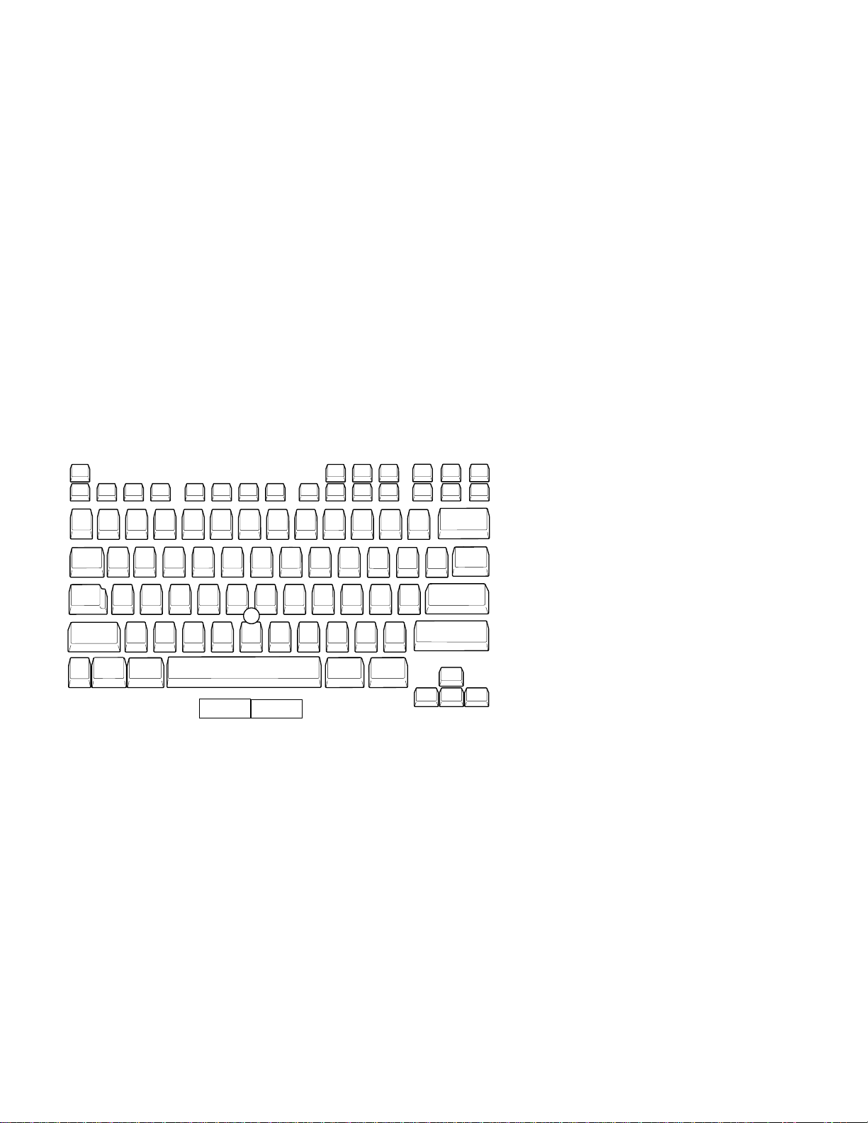
Figure 2-3 shows the key numbers assigned to keys on the 84-key
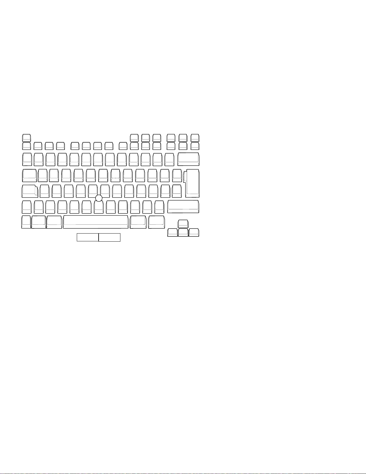
keyboard (for the U.S. and Japan). Figure 2-4 on page 2-6 shows
the key numbers assigned to keys on the 85-key keyboard (for
countries other than the U.S. and Japan). For scan codes assigned
to each numbered key, refer to the
Interface Technical Reference
IBM Personal System/2 Hardware
.
110
112
113
1
16
30 31
44
Fn
114
2
3
17
18
46
58
60
116
115
4
19
32
47
5
33
48
117 118 119
6
20
21
34
35 36
49
Left Right
7
22
50 51
61
8
120
9
23 24
37
52 53
124
125
122 123 76 81
121
10 11
25
38
39
62 64
Figure 2-3. Key Numbers for the 84-Key Keyboard
54
126
12
26
40 41
55
80
75
13
27
79
85
86
15
29
28
43
57
83
89
84
ThinkPad 560/560E System Board 2-5
Page 28
110
112
113
1
16
30 31
44
Fn
124
125
126
114
2
3
17
18
46
45
58
60
116
115
4
19
32
47
5
33
48
117 118 119
6
20
21
34
35 36
49
Left Right
7
22
50 51
61
8
23 24
120
37
121
9
10 11
38
52 53
122 123 76 81
12
26
25
39
62 64
54
27
40 41
55
80
75
13
28
42
79
85
86
15
43
57
83
89
84
Figure 2-4. Key Numbers for the 85-Key Keyboard
Keyboard ID
The keyboard ID consists of 2 bytes: hex 83AB (the built-in keyboard
with the external numeric keypad) or hex 84AB (the built-in keyboard
only). Interrupt 16H, function code (AH)=0AH, returns the keyboard
ID.
2-6 ThinkPad 560/560E System Board
Page 29

Figure 2-5 shows the key numbers assigned to keys on the external
numeric keypad. For scan codes assigned to each numbered key,
refer to the
Reference
IBM Personal System/2 Hardware Interface Technical
.
90 95
91
96
92
97
93
98
99
100
101
102
103
104
105
106
108
Figure 2-5. Key Numbers for the External Numeric Keypad
Displayable Characters and Symbols
For displayable characters and symbols that are keyable from the
keyboard, refer to the
Technical Reference
IBM Personal System/2 Hardware Interface
.
ThinkPad 560/560E System Board 2-7
Page 30

Hard Disk Drive Connector
The hard disk drive is connected to the system board. The following
shows the pin assignments for the connector on the system board.
1
49
2
Pin Signal Description Pin Signal Description
1 JP1 Jumper
(master)
2 JP1 Jumper
(master)
3 JP2 Jumper (slave) 28 GND Ground
4 JP2 Jumper (slave) 29 −HIOW I/O write
5 – Not connected 30 GND Ground
6 – Not connected 31 −HIOR I/O read
7 −HRESET Reset 32 GND Ground
8 GND Ground 33 IORDY I/O ready
9 HD07 Data 7 34 – Not connected
10 HD08 Data 8 35 – Not connected
11 HD06 Data 6 36 GND Ground
12 HD09 Data 9 37 HIRQ Interrupt
13 HD05 Data 5 38 – Not connected
14 HD10 Data 10 39 HA01 Address 1
15 HD04 Data 4 40 – Not connected
16 HD11 Data 11 41 HA00 Address 0
17 HD03 Data 3 42 HA02 Address 2
18 HD12 Data 12 43 −HCS0 Chip select 0
19 HD02 Data 2 44 −HCS1 Chip select 1
20 HD13 Data 13 45 −DASP Drive
21 HD01 Data 1 46 GND Ground
22 HD14 Data 14 47 +5V +5V dc
23 HD00 Data 0 48 +5V +5V dc
24 HD15 Data 15 49 GND Ground
25 GND Ground 50 – Not connected
26 – Not connected
27 – Not connected
50
Request
(active/slave
drive present)
Figure 2-6. Hard Disk Drive Connector Pin Assignments
2-8 ThinkPad 560/560E System Board
Page 31

External Connector
The Port Replicator is connected through the 100-pin external
connector at the bottom of the computer. This connector is installed
on the system board and has the following pin assignments:
(Rear of the Computer)
100 51
50 1
Pin Signal Type Pin Signal Type
1 GND G 51 GND G
2 NC – 52 NC –
3 AC/DC Power W 53 AC/CD Power W
4 AC/DC Power W 54 AC/DC Power W
5 AC/DC Power W 55 AC/DC Power W
6 AC/DC Power W 56 AC/DC Power W
7 NC – 57 NC –
8 GND G 58 GND G
9 NC – 59 NC –
10 5V W 60 5V W
11 NC – 61 NC –
12 GND G 62 GND G
13 GND G 63 NC –
14 Data Rate Select1F64−Index F
15 −Drive Select 1 F 65 NC –
16 Data Rate Select0F66NC –
17 −Motor Enable 0 F 67 −Track 0 F
18 −Direction In F 68 NC –
19 −Step F 69 −Write Protect F
20 Write Data F 70 Read Data F
21 −Write Enable F 71 GND G
22 −Head 1 Select F 72 −Diskette
Change
Type Legend:
G: Ground W: Power line
F: Diskette drive signal K: Keyboard/Mouse signal
S: Serial port signal P: Parallel port signal
V: Video signal
F
Figure 2-7 (Part 1 of 2). 100-Pin External Connector Pin Assignments
ThinkPad 560/560E System Board 2-9
Page 32

Pin Signal Type Pin Signal Type
23 GND G 73 GND G
24 NC – 74 SAFE5V W
25 Mouse Data K 75 Keyboard Data K
26 Mouse Clock K 76 Keyboard Clock K
27 GND G 77 GND G
28 NC – 78 NC –
29 NC – 79 NC –
30 GND G 80 GND G
31 Ring Indicator S 81 Data Terminal
Ready
32 Clear to Send S 82 Transmit Data S
33 Request to Send S 83 Receive Data S
34 Data Set Ready S 84 Data Carrier
Detect
35 GND G 85 GND G
36 GND G 86 −STROBE P
37 −AUTO FD XT P 87 Data Bit 0 P
38 −ERROR P 88 Data Bit 1 P
39 −INIT P 89 Data Bit 2 P
40 −SLCT IN P 90 Data Bit 3 P
41 Data Bit 4 P 91 Data Bit 5 P
42 Data Bit 6 P 92 Data Bit 7 P
43 −ACK P 93 BUSY P
44 PE P 94 SLCT P
45 GND G 95 GND G
46 RED V 96 −VIDEO_PDN V
47 BLUE V 97 GREEN V
48 HSYNC V 98 DDCDATA V
49 VSYNC V 99 DDCCLOCK V
50 GND G 100 GND G
Type Legend:
G: Ground W: Powerline
F: Diskette drive signal K: Keyboard/Mouse signal
S: Serial port signal P: Parallel port signal
V: Video signal
S
S
Figure 2-7 (Part 2 of 2). 100-Pin External Connector Pin Assignments
2-10 ThinkPad 560/560E System Board
Page 33

Diskette Drive and Controller
Figure 2-8 shows the read, write, and format capabilities of the
diskette drive for the ThinkPad computer.
Format Size
Diskette Type
3.5-inch 1.0MB Diskette RWF − −
3.5-inch 2.0MB Diskette − RWF RWF
Legend: :
1KB (kilobyte) 1024 bytes
1MB (megabyte) 1 048 576 bytes
R Read
W Write
F Format
Figure 2-8. Diskette Drive Read, Write, and Format Capabilities
720KB 1.2MB 1.44MB
ThinkPad 560/560E System Board 2-11
Page 34

Diskette Drive Connector
The external diskette drive is connected through the diskette drive
connector, located on the left side of the computer. Figure 2-9
shows the pin assignments of the connector:
25
1
26
Pin Signal Type
1 GND Ground
2 DRATE1 Data Rate Select 1
3 VCC5B +5V dc
4– Reserved
5 GND Ground
6– Reserved
7 GND Ground
8 −INDEX Index
9– Reserved
10 – Reserved
11 −DRVSEL0 Drive Select 0
12 DRATE0 Data Rate Select 0
13 −MOTEN0 Motor Enable 0
14 – Reserved
15 −FDIR Direction In
16 −FSTEP Step
17 WRDATA Write Data
18 −FWREN Write Enable
19 GND Ground
20 −TRAK0 Track 0
21 – Reserved
22 −FWPROTECT Write Protect
23 RDDATA Read Data
24 −FSIDE1SEL Side 1 Select
25 – Reserved
26 −DISKCHG Disk Change
2
Figure 2-9. Diskette Drive Connector Pin Assignments
2-12 ThinkPad 560/560E System Board
Page 35

Memory
The ThinkPad computers use the following types of memory:
Read-only memory (ROM)
Random access memory (RAM)
Real-time clock/complementary metal-oxide semiconductor RAM
(RT/CMOS RAM)
ROM Subsystem
The ROM subsystem consists of four banks of 128KB memory.
ROM is active when power is turned on and is assigned to the top of
the first and last 1MB of address space (hex 000F0000–000FFFFF
and hex FFFF0000–FFFFFFFF). After POST checks that system
memory is operating correctly, the ROM code is copied to RAM at
the same address space, and ROM is disabled.
RAM Subsystem
The RAM subsystem on the system board starts at address
hex 00000000 of the address space. The RAM subsystem for the
ThinkPad 560 is 64 bits wide.
The 8MB (ThinkPad 560) or 16MB (ThinkPad 560E) base memory is
on the system board. One 144-pin 8-byte dual inline memory
module (DIMM) connector is provided on the system board. This
connector accepts a 8MB, 16MB, 32MB, or 64MB
1
DIMM. The
memory capacity can be increased up to 40MB (ThinkPad 560) or
80MB (ThinkPad 560E) when a DIMM is used (see “System Board
Memory Connector for DIMM” on page 2-14).
The total amount of usable memory is less than the amount of
memory installed because of ROM-to-RAM remapping and power
management.
1
A 64MB DIMM is supported by ThinkPad 560E only.
ThinkPad 560/560E System Board 2-13
Page 36

System Memory Map
Memory is mapped by the memory controller registers.
Figure 2-10 shows the memory map for a correctly functioning
system. Memory can be mapped differently if POST detects an error
in system board memory or RT/CMOS RAM. In the figure, the
variable
memory starting at or above the hex 100000 boundary.
Hex Address Range Function
00000000 to 0009FFFF 640KB system board RAM
000A0000 to 000BFFFF Video RAM
000C0000 to 000C7FFF System board video BIOS ROM mapped to
000C8000 to 000EFFFF Channel ROM
000F0000 to 000FFFFF 64KB system board ROM mapped to RAM
00100000 to (00100000 +
x
FFFF0000 to FFFFFFFF 64KB system board ROM
Figure 2-10. System Memory Map
MB)
x
represents the number of 1MB blocks of system board
RAM
x
MB system board RAM
(same as 000F0000 to 000FFFFF)
System Board Memory Connector for DIMM
The system board of ThinkPad 560 has one DIMM connector that
directly accepts one 144-pin DIMM of one of the following three
different capacities: 8MB, 16MB, or 32MB.
The system board of ThinkPad 560E has one DIMM connector that
directly accepts one 144-pin DIMM of one of the following four
different capacities: 8MB, 16MB, 32MB, or 64MB (2-bank type).
Figure 2-11 on page 2-15 shows the pin assignments for the DIMM
connector.
2-14 ThinkPad 560/560E System Board
Page 37

Pin Signal Pin Signal Pin Signal
1 Ground 49 MD42 97 MD25
2 Ground 50 MD21 98 MD38
3 MD15 51 MD41 99 MD24
4 MD48 52 MD22 100 MD39
5 MD14 53 MD40 101 +3.3V dc
6 MD49 54 MD23 102 +3.3V dc
7 MD13 55 Ground 103 MA6
8 MD50 56 Ground 104 MA7
9 MD12 57 Ground 105 MA8
10 MD51 58 Ground 106 MA11
11 +3.3V dc 59 Ground 107 Ground
12 +3.3V dc 60 Ground 108 Ground
13 MD11 61 not connected 109 MA9
14 MD52 62 Not connected 110 Ground
15 MD10 63 +3.3V dc 111 MA10
16 MD53 64 +3.3V dc 112 Ground
17 MD9 65 Not connected 113 +3.3V dc
18 MD54 66 Not connected 114 +3.3V dc
19 MD8 67 −WE 115 −CAS3
20 MD55 68 Not connected 116 −CAS4
21 Ground 69 −RAS2 117 −CAS7
22 Ground 70 Not connected 118 −CAS0
23 −CAS1 71 −RAS3 119 Ground
24 −CAS6 72 Not connected 120 Ground
25 −CAS5 73 Ground 121 MD56
26 −CAS2 74 Not connected 122 MD7
27 +3.3V dc 75 Ground 123 MD57
28 +3.3V dc 76 Ground 124 MD6
29 MA0 77 Ground 125 MD58
30 MA3 78 Ground 126 MD5
31 MA1 79 Ground 127 MD59
32 MA4 80 Ground 128 MD4
33 MA2 81 +3.3V dc 129 +3.3V dc
34 MA5 82 +3.3V dc 130 +3.3V dc
35 Ground 83 MD31 131 MD60
36 Ground 84 MD32 132 MD3
37 MD47 85 MD30 133 MD61
38 MD16 86 MD33 134 MD2
39 MD46 87 MD29 135 MD62
40 MD17 88 MD34 136 MD1
41 MD45 89 MD28 137 MD63
42 MD18 90 MD35 138 MD0
43 MD44 91 Ground 139 Ground
44 MD19 92 Ground 140 Ground
45 +3.3V dc 93 MD27 141 IòC Data
46 +3.3V dc 94 MD36 142 IòC Clock
47 MD43 95 MD26 143 +3.3V dc
48 MD20 96 MD37 144 +3.3V dc
Figure 2-11. DIMM Connector Pin Assignments
ThinkPad 560/560E System Board 2-15
Page 38

RT/CMOS RAM
The RT/CMOS RAM (real-time clock/complementary metal-oxide
semiconductor RAM) module contains the real-time clock and 128
bytes of CMOS RAM. The clock circuitry uses 14 bytes of this
memory; the remainder is allocated to configuration and
system-status information. A battery is built into the module to keep
the RT/CMOS RAM active when the power supply is not turned on.
Figure 2-12 lists the RT/CMOS RAM bytes and their addresses.
Address (Hex) RT/CMOS RAM Bytes
000–00D Real-time clock
00E Diagnostic status
00F Shutdown status
010 Diskette drive type
011 Hard disk 2 and 3 drive type
012 Hard disk 0 and 1 drive type
013 Reserved
014 Equipment
015, 016 Low and high base memory
017, 018 Low and high expansion memory
019 Hard disk 0 extended byte
01A Hard disk 1 extended byte
01B Hard disk 2 extended byte
01C Hard disk 3 extended byte
01D–02D Reserved
02E, 02F Checksum
030, 031 Low and high usable memory above 1MB
032 Date-century
033–07F Reserved
Figure 2-12. RT/CMOS RAM Address Map
2-16 ThinkPad 560/560E System Board
Page 39

RT/CMOS Address and NMI Mask Register (Hex 0070)
The NMI mask register is used with the RT/CMOS data register (hex
0071) to read from and write to the RT/CMOS RAM bytes.
Attention
The operation following a write to hex 0070 should access hex
0071; otherwise, intermittent failures of the RT/CMOS RAM can
occur.
Bit Function
7 NMI mask
6–0 RT/CMOS RAM address
Figure 2-13. RT/CMOS Address and NMI Mask Register (Hex 0070)
Bit 7 When this write-only bit is set to 1, the NMI is masked
(disabled). This bit is set to 1 by a power-on reset.
Bits 6–0 These bits are used to select RT/CMOS RAM
addresses.
RT/CMOS Data Register (Hex 0071)
The RT/CMOS data register is used with the RT/CMOS address and
NMI mask register (hex 0070) to read from and write to the
RT/CMOS RAM bytes.
Bit Function
7–0 RT/CMOS data
Figure 2-14. RT/CMOS Data Register (Hex 0071)
ThinkPad 560/560E System Board 2-17
Page 40

RT/CMOS RAM I/O Operations
During I/O operations to the RT/CMOS RAM addresses, you should
mask interrupts to prevent other interrupt routines from changing the
RT/CMOS address register before data is read or written. After I/O
operations, you should leave the RT/CMOS address and NMI mask
register (hex 0070) pointing to status register D (hex 00D).
Attention
The operation following a write to hex 0070 should access hex
0071; otherwise, intermittent failures of the RT/CMOS RAM can
occur.
Writing to the RT/CMOS RAM requires the following:
1. Write the RT/CMOS RAM address to the RT/CMOS address and
NMI mask register (hex 0070).
2. Write the data to the RT/CMOS data register (hex 0071).
3. Write the address, hex 0F, to the RT/CMOS and NMI mask
register; this leaves hex 0070 pointing to the shutdown status
byte (hex 0F).
4. Read address hex 0071 to restore the RT/CMOS.
Reading from the RT/CMOS RAM requires the following steps:
1. Write the RT/CMOS RAM address to the RT/CMOS and NMI
mask register (hex 0070).
2. Read the data from the RT/CMOS data register (hex 0071).
3. Write the address, hex 0F, to the RT/CMOS and NMI mask
register; this leaves hex 0070 pointing to the shutdown status
byte (hex 0F).
4. Read address hex 0071 to restore the RT/CMOS.
2-18 ThinkPad 560/560E System Board
Page 41

Real-Time Clock Bytes (Hex 000–00D):
Bit definitions and
addresses for the real-time clock bytes are shown in Figure 2-15.
Address
(Hex)
000 Seconds 0
001 Second alarm 1
002 Minutes 2
003 Minute alarm 3
004 Hours 4
005 Hour alarm 5
006 Day of week 6
007 Date of month 7
008 Month 8
009 Year 9
00A Status register A 10
00B Status register B 11
00C Status register C 12
00D Status register D 13
Figure 2-15. Real-Time Clock Bytes (Hex 000–00D)
Function
Byte Number
Note: The Setup program initializes status registers A and B when
the time and date are set. Interrupt 1AH is the BIOS
interface to read and set the time and date; it initializes the
registers in the same way that the Setup program does.
Status Register A (Hex 00A)
Bit Function
7 Update in progress
6–4 22-stage divider
3–0 Rate-selection bits
Figure 2-16. Status Register A (Hex 00A)
Bit 7 When set to 1, this bit indicates that the time-update
cycle is in progress. When set to 0, it indicates that the
current date and time can be read.
Bits 6–4 These bits identify which time-base frequency is being
used. The system initializes these bits to binary 010,
which selects a 32.768-kHz time base. This is the only
value supported by the system for proper timekeeping.
Bits 3–0 These bits allow the selection of a divider output
frequency. The system initializes the rate-selection bits
to a binary 0110, which selects a 1.024-kHz
ThinkPad 560/560E System Board 2-19
Page 42

square-wave output frequency and a
976.562-microsecond periodic interrupt rate.
Status Register B (Hex 00B)
Bit Function
7 Set
6 Enable periodic interrupt
5 Enable alarm interrupt
4 Enable update-ended interrupt
3 Enable square wave
2 Date mode
1 24-hour mode
0 Enable daylight-saving time
Figure 2-17. Status Register B (Hex 00B)
Bit 7 When set to 0, this bit updates the cycle, normally by
advancing the count at a rate of one cycle per second.
When set to 1, it immediately ends any update cycle in
progress, and the program can initialize the 14 time bytes
without any further updates occurring until this bit is set
to 0.
Bit 6 This is a read/write bit that allows an interrupt to occur at
a rate specified by the rate and divider bits in status
register A. When set to 1, this bit enables the interrupt.
The system initializes this bit to 0.
Bit 5 When set to 1, this bit enables the alarm interrupt. The
system initializes this bit to 0.
Bit 4 When set to 1, this bit enables the update-ended
interrupt. The system initializes this bit to 0.
Bit 3 When set to 1, this bit enables the square-wave
frequency as set by the rate-selection bits in status
register A. The system initializes this bit to 0.
Bit 2 This bit indicates whether the binary-coded-decimal (BCD)
or binary format is used for time-and-date calendar
updates. When set to 1, this bit indicates the binary
format. The system initializes this bit to 0.
Bit 1 This bit indicates whether the hours byte is in 12-hour or
24-hour mode. When set to 1, this bit indicates the
24-hour mode. The system initializes this bit to 1.
2-20 ThinkPad 560/560E System Board
Page 43

Bit 0 When set to 1, this bit enables the daylight-saving-time
mode. When set to 0, this bit disables the
daylight-saving-time mode, and the clock reverts to
standard time. The system initializes this bit to 0.
Status Register C (Hex 00C)
Bit Function
7 Interrupt request flag
6 Periodic interrupt flag
5 Alarm interrupt flag
4 Update-ended interrupt flag
3–0 Reserved
Figure 2-18. Status Register C (Hex 00C)
Note: Interrupts are enabled by bits 6, 5, and 4 in status register B.
Bit 7 When set to 1, this bit indicates that an interrupt has
occurred; bits 6, 5, and 4 indicate the type of interrupt.
Bit 6 When set to 1, this bit indicates that a periodic interrupt
has occurred.
Bit 5 When set to 1, this bit indicates that an alarm interrupt
has occurred.
Bit 4 When set to 1, this bit indicates that an update-ended
interrupt has occurred.
Bits 3–0 These bits are reserved.
Status Register D (Hex 00D)
Bit Function
7 Valid RAM
6–0 Reserved
Figure 2-19. Status Register D (Hex 00D)
Bit 7 This read-only bit monitors the internal battery. When
set to 1, this bit indicates that the real-time clock has
power. When set to 0, it indicates that the real-time
clock has lost power and the data in CMOS is no longer
valid.
Bits 6–0 These bits are reserved.
ThinkPad 560/560E System Board 2-21
Page 44

CMOS RAM Configuration
Figure 2-20 shows the bit definitions for the CMOS RAM
configuration bytes.
Diagnostic Status Byte (Hex 00E)
Bit Function
7 Real-time clock power
6 Configuration record and checksum status
5 Incorrect configuration
4 Memory size mismatch
3 Hard disk controller/drive C initialization status
2 Time status indicator
1, 0 Reserved
Figure 2-20. Diagnostic Status Byte (Hex 00E)
Bit 7 When set to 1, this bit indicates that the real-time clock
has lost power.
Bit 6 When set to 1, this bit indicates that the checksum is
incorrect.
Bit 5 This bit indicates the results of a power-on check of the
equipment byte (hex 014). When set to 1, this bit
indicates that the configuration information is incorrect.
Bit 4 When set to 1, this bit indicates that the memory size
does not match the configuration information.
Bit 3 When set to 1, this bit indicates that the controller or hard
disk drive failed initialization.
Bit 2 When set to 1, this bit indicates that the time is invalid.
Bits 1, 0 These bits are reserved.
Shutdown Status Byte (Hex 00F):
power-on diagnostic programs.
2-22 ThinkPad 560/560E System Board
This byte is defined by the
Page 45

Diskette Drive Type Byte (Hex 010):
This byte indicates the type
of the installed diskette drive.
Bit Drive Type
7–4 Diskette drive type
3–0 Reserved
Figure 2-21. Diskette Drive Type Byte (Hex 010)
Bits 7–4 These bits indicate the diskette drive type.
Bits 7–4 Description
0 1 1 0
0 1 0 0
Note: Combinations not shown are reserved.
Diskette drive (2.88MB)
Diskette drive (1.44MB)
Figure 2-22. Diskette Drive Type Bits 7–4
Bits 3–0 These bits are reserved.
Hard Disk Drive Type Byte (Hex 011):
This byte defines the type
of hard disk drive installed. Hex 00 indicates that no hard disk drive
is installed.
Bit Drive Type
7–4
3–0
Hard disk drive type 2
Hard disk drive type 3
Figure 2-23. Hard Disk Type Byte (Hex 011)
Bit 7–4 Description
0 0 0 0
1 1 1 1
No drive installed for hard disk drive 2
Use CMOS 1BH for hard disk drive 2
Figure 2-24. Hard Disk Drive Type 2 (Bits 7–4)
Bit 3–0 Description
0 0 0 0
1 1 1 1
No drive installed for hard disk drive 3
Use CMOS 1CH for hard disk drive 3
Figure 2-25. Hard Disk Drive Type 3 (Bits 3–0)
ThinkPad 560/560E System Board 2-23
Page 46

Hard Disk Drive Type Byte (Hex 012):
This byte defines the type
of hard disk drive installed. Hex 00 indicates that no hard disk drive
is installed.
Bit Drive Type
7–4 Hard disk drive 0
3–0 Hard disk drive 1
Figure 2-26. Hard Disk Drive Type Byte
Reserved Bytes (Hex 013):
Equipment Byte (Hex 014):
These bytes are reserved.
This byte defines the basic equipment
in the system for the power-on diagnostic tests.
Bit Description
7, 6 Number of diskette drives
5, 4 Display operating mode
3, 2 Reserved
1 Coprocessor presence
0 Diskette drive 0 presence
Figure 2-27. Equipment Byte
Bits 7, 6 These bits indicate the number of installed diskette
drives.
Bits 7,6 Number of Diskette Drives
0 0 One drive
0 1 Reserved
1 0 Reserved
1 1 Reserved
Figure 2-28. Installed Diskette Drive Bits
Bits 5, 4 These bits indicate the operating mode of the display
attached to the video port.
Bits 5,4 Display Operating Mode
0 0 Reserved
0 1 40-column mode
1 0 80-column mode
1 1 Monochrome mode
Figure 2-29. Display Operating Mode Bits
2-24 ThinkPad 560/560E System Board
Page 47

Bits 3–2 These bits are reserved.
Bit 1 When set to 1, this bit indicates that a coprocessor is
installed.
Bit 0 When set to 1, this bit indicates that physical diskette
drive 0 is installed.
Low and High Base Memory Bytes (Hex 015 and Hex 016):
The
low and high base memory bytes define the amount of memory
below the 640KB address space.
The value in these bytes represents the number of 1KB blocks of
base memory. For example, hex 0280 indicates 640KB. The low
byte is hex 015; the high byte is hex 016.
Low and High Expansion Memory Bytes (Hex 017 and Hex
018):
The low and high expansion memory bytes define the amount
of memory above the 1MB address space.
The value in these bytes represents the number of 1KB blocks of
expansion memory. For example, hex 0800 indicates 2048KB. The
low byte is hex 017; the high byte is hex 018.
Reserved Bytes (Hex 01D–02D):
Configuration Checksum Bytes (Hex 02E and Hex 02F):
These bytes are reserved.
The
configuration checksum bytes contain the checksum character for
bytes hex 010 through hex 02D of the 64-byte CMOS RAM. The
high byte is hex 02E; the low byte is hex 02F.
Low and High Usable Memory Bytes (Hex 030 and Hex 031):
The low and high usable memory bytes define the total amount of
contiguous memory from 1MB to 20MB.
The hexadecimal values in these bytes represent the number of 1KB
blocks of usable memory. For example, hex 0800 is equal to
2048KB. The low byte is hex 30; the high byte is hex 31.
Date-Century Byte (Hex 032):
Bits 7 through 0 of the date-century
byte contain the binary-coded decimal value for the century. For
information about reading and setting this byte, refer to the
Personal System/2 and Personal Computer BIOS Interface
Reserved Bytes (Hex 033–07F):
These bytes are reserved.
ThinkPad 560/560E System Board 2-25
IBM
.
Page 48

Miscellaneous System Functions and Ports
This section provides information about nonmaskable interrupts
(NMIs), the power-on password, and hardware compatibility.
Nonmaskable Interrupt (NMI)
The NMI signals the system microprocessor that a parity error or a
channel check timeout has occurred. This situation can cause lost
data or an overrun error on some I/O devices. The NMI masks all
other interrupts. The interrupt return (IRET) instruction restores the
interrupt flag to the state it was in before the interrupt occurred. A
system reset causes a reset of the NMI.
The NMI requests from system board parity and channel check are
subject to mask control with the NMI mask bit in the RT/CMOS
Address register. See “RT/CMOS Address and NMI Mask Register
(Hex 0070)” on page 2-17. The power-on default of the NMI mask is
1 (NMI disabled). Before the NMI is enabled after a power-on reset,
the parity-check states are initialized by POST.
Attention
The operation following a write to hex 0070 should access hex
0071; otherwise, intermittent failures of the RT/CMOS RAM can
occur.
2-26 ThinkPad 560/560E System Board
Page 49

System Control Port B (Hex 0061)
Bit definitions for the write and read functions of this port are shown
in the following figures:
Bit Function
7–4 Reserved
3 Reserved (should be 0)
2 Enable parity check
1 Enable speaker data
0 Timer 2 gate to speaker
Figure 2-30. System Control Port B (Hex 0061, Write)
Bit Function
7 Parity check
6 Channel check
5 Timer 2 output
4 Toggles with each refresh request
3 Reserved
2 Enable parity check
1 Enable speaker data
0 Timer 2 gate to speaker
Figure 2-31. System Control Port B (Hex 0061, Read)
Bit 7 When set to 1, this bit indicates that the PCI System Error
(SERR#) was pulsed active.
Bit 6 When set to 1, this bit indicates a channel check has
occurred.
Bit 5 When read, this bit indicates the condition of the
timer/counter 2 ‘output’ signal.
Bit 4 When read, this bit toggles for each refresh request.
Bit 3 Reserved.
Bit 2 When set to 0, this bit enables the PCI System Error
(SERR#). This bit is set to 1 during a power-on reset.
Bit 1 When set to 1, this bit enables the speaker data.
Bit 0 When set to 1, this bit enables the timer 2 gate.
ThinkPad 560/560E System Board 2-27
Page 50

System Control Port A (Hex 0092)
Bit Function
7–3 Reserved
2 Reserved (must be set to 0)
1 Alternate gate A20
0 Alternate hot reset
Figure 2-32. System Control Port A (Hex 0092)
Bits 7–3 These bits are reserved.
Bit 2 This bit is reserved.
Bit 1 This bit is used to enable the ‘address 20’ signal (
when the microprocessor is in the real address mode.
When this bit is set to 0, A20 cannot be used in real
mode addressing. This bit is set to 0 during a system
reset.
Bit 0 This bit provides an alternative method of resetting the
system microprocessor. This alternative method
supports operating systems requiring faster operation
than that provided on the IBM Personal Computer AT.
Resetting the system microprocessor switches the
microprocessor from protected mode to real address
mode.
This bit is set to 0 by either a system reset or a write
operation. When a write operation changes this bit from
0 to 1, the ‘processor reset’ signal is pulsed after the
reset has occurred. While the reset is occurring, the
latch remains set so that POST can read this bit. If the
bit is set to 0, POST assumes that the system was just
powered on. If the bit is set to 1, POST assumes that
the microprocessor has been switched from protected
mode to real mode.
When bit 0 is used to reset the system microprocessor
to the real mode, use the following procedure:
1. Disable all maskable and nonmaskable interrupts.
2. Reset the system microprocessor by writing a 1 to
bit 0.
3. Issue a Halt instruction to the system
microprocessor.
4. Reenable all maskable and nonmaskable interrupts.
A20)
2-28 ThinkPad 560/560E System Board
Page 51

If you do not follow this procedure, the results are
unpredictable.
Note: Whenever possible, use BIOS as an interface to
reset the system microprocessor to the real
mode. For more information about resetting the
system microprocessor, refer to the
IBM Personal
System/2 and Personal Computer BIOS
Interface
.
Power-On Password
RT/CMOS RAM has 8 bytes reserved for the power-on password
and the check character. The 8 bytes are initialized to hex 00. The
microprocessor can access these bytes only during POST. After
POST is completed, if a power-on password is installed, the
password bytes are locked and cannot be accessed by any program.
During power-on password installation, the password (1 to 7
characters) is stored in the security space.
Installing the password is a function of the built-in system program
Easy-Setup
when it is installed, changed, or removed. After the power-on
password has been installed, it can be changed or removed only
during POST.
. The power-on password does not appear on the screen
The computer also can have a keyboard password. For more
information, see the keyboard and auxiliary device controller section
of the
IBM Personal System/2 Hardware Interface Technical
Reference
.
Selectable Drive-Startup Sequence
Selectable drive-startup (selectable boot) allows you to control the
startup sequence of the drives in your computer. The order in which
the computer looks for the drives for your operating system is the
drive-startup sequence
systems, you might want to change the drive-startup sequence to
load the operating system from the hard disk without first checking
the diskette drive, or to do a remote program load (RPL).
. If you are working with multiple operating
ThinkPad 560/560E System Board 2-29
Page 52

Attention
When changing your startup sequence, you must be extremely
careful when doing write operations (such as copying, saving, or
formatting). Your data or programs can be overwritten if you
select the wrong drive.
For more information about the selectable drive-startup sequence,
refer to the
Hardware Compatibility
The computer supports most of the interfaces used by the IBM
Personal Computer AT* and the Personal System/2* (PS/2*)
products. In many cases, command and status organization of these
interfaces are maintained.
The functional interfaces for the computer are compatible with the
following:
The Intel 8259 interrupt controllers (edge trigger mode).
The Intel 8254 timers driven from 1.193 MHz (channels 0, 1, and
2).
The Intel 8237 DMA controller-address/transfer counters, page
registers, and status fields only. The command and request
registers, and the rotate and mask functions, are not supported.
The mode register is partially supported.
The NS16550 serial communications controller.
The Intel Pentium microprocessor (ThinkPad 560)
the Intel Pentium processor with the MMX technology (ThinkPad
560E).
The Intel 8086**, 8088**, 80286**, 80386**, and i486DX
microprocessors.
The Intel 8087**, 80287**, 80387** math coprocessors.
The Intel 82077AA** diskette drive controller.
The keyboard interface at addresses hex 0060 and hex 0064.
Display modes supported by the IBM Monochrome Display and
Printer Adapter, the IBM Color/Graphics Monitor Adapter, and the
IBM Enhanced Graphics Adapter.
ThinkPad User's Guide
.
or
2-30 ThinkPad 560/560E System Board
Page 53

The parallel printer ports (Parallel 1, Parallel 2, and Parallel 3) in
compatibility mode.
Error Codes
POST returns a three or more character code message to indicate
the type of test that failed. Figure 2-33 lists the failure indicated with
the associated error code.
Error
Code
101 Interrupt failure.
102 Timer failure.
103 Timer interrupt failure.
104 Protected mode failure.
105 Last 8042 command not accepted.
107 NMI test failure.
108 Timer bus test failure.
109 Low meg-chip select test.
110 Planar parity.
111 I/O parity.
118 Planar parity error logged.
158 A supervisor password is set, but no hard disk password is set.
159 The hard disk password is not identical to the supervisor password.
161 Dead battery.
163 Date and time are not set; clock not updated.
173 CMOS CRC error.
174 Configuration error.
175 Bad EEPROM CRC 1.
177 Bad supervisor password checksum.
178 EEPROM is not functional.
179 NVRAM error log full.
183 Supervisor password is needed.
184 Bad power-on password checksum.
185 Corrupted startup boot sequence.
186 Inconsistency between EEPROM and security lock latch 2.
188 Bad EEPROM CRC 2.
189 Too many passwords attempted.
190 Critically low battery condition detected.
191XX PM initialization error.
195 Configuration mismatch error found during hibernation wake-up.
196 Critical error found during hibernation wake-up.
201 Memory data error.
202 Memory line error 00 through 15.
203 Memory line error 16 through 23.
215 Memory test failure on on-board memory.
221 ROM to RAM remap error.
301 Keyboard error.
Description
Figure 2-33 (Part 1 of 2). Error Codes
ThinkPad 560/560E System Board 2-31
Page 54

Error
Code
601 Diskette drive or controller error.
602 No valid boot record on diskette.
604 Invalid diskette drive error.
1101 Serial-A test failure.
1201 Serial-B test failure.
1701 Hard disk controller failure.
1780, 1790 Hard disk 0 error.
1781, 1791 Hard disk 1 error.
2401 System board video error.
8081 PCMCIA presence test failure (PCMCIA revision number also
8082 PCMCIA register test failure.
8601 System bus error (8042 mouse interface).
8602 External mouse error.
8603 System bus error or mouse error.
8611 System bus error (I/F between 8042 and IPDC).
8612 TrackPoint III error.
8613 System board or TrackPoint III error.
I9990301 Hard disk error.
I9990302 Invalid hard disk boot record.
I9990303 Bank-2 flash ROM checksum error.
I9990305 No bootable device.
Description
checked).
Figure 2-33 (Part 2 of 2). Error Codes
2-32 ThinkPad 560/560E System Board
Page 55

Section 3. Subsystems
Video Subsystem . . . . . . . . . . . . . . . . . . . . . . . . . . . 3-2
Video Modes . . . . . . . . . . . . . . . . . . . . . . . . . . . . 3-3
Audio Subsystem . . . . . . . . . . . . . . . . . . . . . . . . . . . 3-6
Sound Blaster Support Function ................ 3-6
Audio Port Specifications ..................... 3-6
Infrared (IR) Subsystem ....................... 3-7
System Settings . . . . . . . . . . . . . . . . . . . . . . . . . . 3-7
PCMCIA Subsystem . . . . . . . . . . . . . . . . . . . . . . . . . 3-7
Pin Assignments . . . . . . . . . . . . . . . . . . . . . . . . . . 3-9
This section describes the video, DSP, IR, and PCMCIA subsystems
of the ThinkPad computers. If also provides the Programmable
Option Select (POS) information for the video, DSP, and IR
subsystems.
Copyright IBM Corp. 1996, 1997 3-1
Page 56

Video Subsystem
The video subsystem consists of the SVGA video controller and
video random-access memory. The video subsystem supports TFT
and DSTN displays.
The video subsystem also supports PS/2 analog displays without any
additional adapters.
Note: Use of any video subsystem features not documented in this
book can result in future incompatibility.
ThinkPad 560
Displaying output on the LCD or both on the LCD and monitor:
Supported Color Depth
Resolution
640×480 256 and 65536 256
800×600 256 and 65536 256
1024×768 (virtual
screen)
TFT models DSTN models
256 and 65536 256
Displaying output on the monitor:
Supported Color Depth
TFT models DSTN models
256, 65536, and
16 777 216
256 and 65536 256 and 65536
256 2561024x768
Resolution
640x480
800x600
Frame
Rate
60Hz
72Hz
75Hz
85Hz
60Hz
75Hz
85Hz
60Hz
75Hz
85Hz
43.5Hz
(interlace)
3-2 ThinkPad 560/560E Subsystems
256, 65536, and
16 777 216
Page 57

ThinkPad 560E
Displaying output on the LCD or both on the LCD and monitor:
Resolution Supported Color Depth
640×480 256, 65 536, and 16777216
800×600
1024×768 (virtual
screen)
256 and 65536
Displaying output on the monitor:
Resolution Refresh Rate Supported Color
640×480 60Hz 256, 65536, and
72Hz
75Hz
85Hz
800×600 60Hz
75Hz
85Hz 256 and 65536
1024×768 60Hz
75Hz
43.5Hz (interlace)
1280×1024 60Hz 256
43.5Hz (interlace)
Depth
16 777 216
Video Modes
The video subsystem supports the modes listed in Table 3-1 on
page 3-4. VESA105 and VESA112 modes are supported only for
the external PS/2 display.
ThinkPad 560/560E Subsystems 3-3
Page 58

3-4 ThinkPad 560/560E Subsystems
Table 3-1 (Page 1 of 2). BIOS Video Modes for the ThinkPad Computer
Mode
(Hex)
0, 1
0*, 1*
0#, 1#
2, 3
2*, 3*
2#, 3#
4, 5
6
7*
7#
D
E
F
10
11
12
13
VESA101
Type
A/N
A/N
A/N
A/N
A/N
A/N
APA
APA
A/N
A/N
APA
APA
APA
APA
APA
APA
APA
APA
Colors
16
16
16
16
16
16
4
2
–
–
16
16
–
16
2
16
256
256
Alpha-
numeric
Format
40×25
40×25
40×25
80×25
80×25
80×25
40×25
80×25
80×25
80×25
40×25
80×25
80×25
80×25
80×30
80×30
40×25
–
Buffer
Start
Address
B8000
B8000
B8000
B8000
B8000
B8000
B8000
B8000
B0000
B0000
A0000
A0000
A0000
A0000
A0000
A0000
A0000
A0000
Box
Size
8×8
8×14
8×16
8×8
8×14
8×16
8×8
8×8
8×14
8×16
8×8
8×8
8×14
8×14
8×16
8×16
8×8
–
Maximum
Pages
8
8
8
8
8
8
1
1
8
8
8
4
2
2
1
1
1
1
Pels
320×200
320×350
320×400
640×200
640×350
640×400
320×200
640×200
640×350
640×400
320×200
640×200
640×350
640×350
640×480
640×480
320×200
640×480
Expanded Size
(to 800×600)
800×600
800×525
800×600
800×600
800×525
800×600
800×600
800×600
800×525
800×600
800×600
800×600
800×525
800×525
800×600
800×600
800×600
800×600
Page 59

ThinkPad 560/560E Subsystems 3-5
Table 3-1 (Page 2 of 2). BIOS Video Modes for the ThinkPad Computer
Mode
(Hex)
VESA103
VESA105
VESA107
VESA110
VESA111
VESA112
VESA114
VESA115
VESA117
Note:
A border screen is not supported on the LCD.
Modes VESA107, VESA115, and VESA117 are supported by ThinkPad 560E only.
Type
APA
APA
APA
APA
APA
APA
APA
APA
APA
Colors
256
256
256
32768
65536
16 777 216
65536
16 777 216
65536
Alpha-
numeric
Format
–
–
–
–
–
–
–
–
–
Buffer
Start
Address
A0000
A0000
A0000
A0000
A0000
A0000
A0000
A0000
A0000
Box
Size
–
–
–
–
–
–
–
–
–
Maximum
Pages
1
1
1
1
1
1
1
1
1
Pels
800×600
1024×768
1280×1024
640×480
640×480
640×480
800×600
800×600
1024×768
Expanded Size
(to 800×600)
–
–
–
–
–
–
–
–
–
Page 60

Audio Subsystem
Sound Blaster Support Function
The Sound Blaster support function provides three system settings:
I/O address, IRQ level, and DMA channel.
I/O Address IRQ Level DMA Channel
0220–022F (Default)
0240–024F
0338–033F (FM synthesizer)
IRQ 5 (Default)
IRQ 7
IRQ 10
IRQ 11
DMA 0
DMA 1 (Default)
–
–
Audio Port Specifications
Audio Output:
– ⅛-inch mini-jack for headphone
– Headphone speaker output: 22 mW (32 ohm) maximum
– Maximum output level: 2.4 V pp
– Output impedance: 75 ohm
Audio Input:
– ⅛-inch mini-jack for microphone or line input
– Microphone gain: 26 dB minimum, 48.5 dB maximum
– Maximum input level:
Microphone: 125 mV pp
Line In: 4.0 V pp
– Input impedance:
Microphone: 47 k ohm
Line In: 30 k ohm
3-6 ThinkPad 560/560E Subsystems
Page 61

Infrared (IR) Subsystem
The IR subsystem of ThinkPad 560 is designed to be compatible
with the IrDA** Serial Infrared Physical Layer Link Specification
Version 1.0 and Data Link Specification Version 1.0.
The IR subsystem of ThinkPad 560E is designed to be compatible
with the IrDA** Serial Infrared Physical Layer Link Specification
Version 1.0 or 1.1 and Data Link Specification Version 1.0.
System Settings
The I/O address can be selected from the following with the system
utility program. The IR subsystem uses one serial port address.
I/O Address
03F8–03FF Serial port 1 (Default)
02F8–02FF Serial port 2
03E8–03EF Serial port 3
02E8–02EF Serial port 4
PCMCIA Subsystem
The system board has two 68-pin PCMCIA (Personal Computer
Memory Card International Association) slots that support three
different types of PC cards: Type I, Type II, and Type III PC cards.
The Type I and Type II PC cards can be installed into either the
upper or the lower slot, or into both slots at the same time. The
Type III PC card, however, must be installed only in the lower slot.
The Type II PC card cannot be used in the upper slot when a Type
III PC card is used.
The PCMCIA slots are designed according to the following PCMCIA
standards and specifications:
ThinkPad 560/560E Subsystems 3-7
Page 62

Standards and Specifications Characteristics
PCMCIA Card Standard Release 2.0 or 2.1
PCMCIA Socket Services Interface Specifications Release 2.0 or 2.1
PCMCIA Card Services Interface Specifications Release 2.0 or 2.1
PC Card Physical Configuration Type II and Type III
Supported voltage 5.0 V dc only
Figure 3-1. PCMCIA Standards and Specifications
3-8 ThinkPad 560/560E Subsystems
Page 63

Pin Assignments
Figure 3-2 shows the pin assignments for the PCMCIA slots.
Pin Signal Pin Signal
1 Ground 35 Ground
2D3 36−CD1
3D4 37D11
4D5 38D12
5D6 39D13
6D7 40D14
7 −CE1 41 D15
8 A10 42 −CE2
9 −OE 43 RFSH
10 A11 44 RFU (−IOR)
11 A9 45 RFU (−IOW)
12 A8 46 A17
13 A13 47 A18
14 A14 48 A19
15 −WE/−PGM 49 A20
16 RDY/−BSY (IREQ) 50 A21
17 +5 V dc 51 +5 V dc
18 V pp1 52 V pp2
19 A16 53 A22
20 A15 54 A23
21 A12 55 A24
22 A7 56 A25
23 A6 57 RFU
24 A5 58 RESET
25 A4 59 −WAIT
26 A3 60 RFU (−INPACK)
27 A2 61 −REG
28 A1 62 BVD2 (−SPKR)
29 A0 63 BVD1 (−STSCHG)
30 D0 64 D8
31 D1 65 D9
32 D2 66 D10
33 WP (−IOIS16) 67 −CD2
34 Ground 68 Ground
Figure 3-2. PCMCIA PC Card Slot Pin Assignments
The maximum current for +5 V dc (±5%) is 0.5 A for each slot, total
of 1.0 A for both slots.
The maximum current for +12 V dc is 0.1 A (including both slots and
V pp). When the computer is in suspend mode, it requires a current
of 0.05 A.
ThinkPad 560/560E Subsystems 3-9
Page 64

3-10 ThinkPad 560/560E Subsystems
Page 65

Appendix A. System Management API (SMAPI) BIOS Overview
What is SMAPI BIOS? ........................ A-3
Header Image . . . . . . . . . . . . . . . . . . . . . . . . . . . . . A-4
Calling Convention . . . . . . . . . . . . . . . . . . . . . . . . . . A-6
Parameter Structure . . . . . . . . . . . . . . . . . . . . . . . A-6
Sample in Assembler Language ............... A-7
Sample in C Language .................... A-8
Calling Convention Pseudo Code ................ A-9
Return Codes . . . . . . . . . . . . . . . . . . . . . . . . . . . . A-11
Function Description . . . . . . . . . . . . . . . . . . . . . . . . A-12
System Information Service .................. A-12
Get System Identification .................. A-12
Get CPU Information .................... A-13
Get Display Device Information .............. A-14
Get Slave Micro Control Unit Information ......... A-15
Get System Sensor Status ................. A-16
Get Video Information .................... A-17
Get Refresh Rate Capability ................ A-18
System Configuration Service ................. A-20
Get Display Device State .................. A-20
Set Display Device State .................. A-22
Get Pointing Device State .................. A-23
Set Pointing Device State .................. A-24
Get Hotkey Sticky/Lock ................... A-25
Set Hotkey Sticky/Lock Support .............. A-26
Power Management Service .................. A-27
Get Power Management Mode (BL=00h) ......... A-27
Set Power Management Mode ............... A-28
Get Timer Control ...................... A-29
Set Timer Control ...................... A-31
Event Bit Definition ....................... A-32
Get System Event Global Condition ............ A-33
Set System Event Global Condition ............ A-34
Get System Event 1 Condition ............... A-35
Set System Event 1 Condition ............... A-36
Get System Event 2 Condition ............... A-37
Set System Event 2 Condition ............... A-38
Get System Timer ...................... A-39
Set System Timer ...................... A-40
Get Standby Timer ...................... A-41
Set Standby Timer ...................... A-42
Copyright IBM Corp. 1996, 1997 A-1
Page 66

Get Hibernation Timer .................... A-43
Set Hibernation Timer .................... A-44
Get System Event 3 Condition ............... A-45
Set System Event 3 Condition ............... A-46
Get System Resume Condition .............. A-47
Set System Resume Condition ............... A-48
Get System Resume Timer ................. A-49
Set System Resume Timer ................. A-50
Request System Standby .................. A-51
Request System Suspend ................. A-51
Request System Hibernation ................ A-52
Request System Off ..................... A-52
Samples . . . . . . . . . . . . . . . . . . . . . . . . . . . . . A-53
Data Structure . . . . . . . . . . . . . . . . . . . . . . . . A-53
Function Declaration . . . . . . . . . . . . . . . . . . . . . . A-57
Installation Check . . . . . . . . . . . . . . . . . . . . . . . . A-58
BIOS Call . . . . . . . . . . . . . . . . . . . . . . . . . . . . . A-62
A-2 ThinkPad 560/560E SMAPI BIOS
Page 67

What is SMAPI BIOS?
The ThinkPad Basic Input/Output System (BIOS) provides a special
software interface, called the System Management Application
Program Interface (SMAPI) BIOS, to control the following unique
features of the ThinkPad system:
System Information
This BIOS provides unique ThinkPad information, such as
the system identifier (system ID).
System Configuration
The ThinkPad SMAPI BIOS provides system configuration
control for such features as display device selection or
resource configuration for built-in devices.
Power Management
Through the SMAPI BIOS, the operating system or
application software can control the ThinkPad power
management features (the Power mode or
Suspend/Hibernation/Resume options).
“Header Image” on page A-4 describes how to use the SMAPI BIOS.
ThinkPad 560/560E SMAPI BIOS A-3
Page 68

Header Image
Systems that support SMAPI BIOS must provide the following header
image in the F000 segment system ROM area at the 16-byte
boundary. The client needs to search and find this SMAPI BIOS
header image to get the entry point for the service.
Field Offset Length Value
Signature 00h 4 bytes '$SMB' (ASCII)
Version (Major) 04h Byte 01h
Version (Minor) 05h Byte 00h
Length 06h Byte 20h
Checksum 07h Byte –
Information Word 08h Word –
Reserved 1 0Ah Word –
Real mode 16-bit offset to entry
point
Real mode 16-bit code segment
address
Reserved 2 10h Word –
16-bit protected mode offset to
entry point
16-bit protected mode code
segment base address
32-bit protected mode offset to
entry point
32-bit protected mode code
segment base address
0Ch Word –
0Eh Word –
12h Word –
14h Dword –
18h Dword –
1Ch Dword –
Signature ASCII Code '$SMB' is stored at the top of the header
image.
Version (Major/Minor)
Indicates the SMAPI BIOS version.
Length The length of the header image.
Checksum Checksum byte area. The client verifies that this
header image is valid by using this checksum; the client
should check all header image bytes, and the result will
be zero bytes.
A-4 ThinkPad 560/560E SMAPI BIOS
Page 69

Information Word
This area identifies the BIOS service level defined
below.
Information Word
Bit ð : Real/V86 mode interface support
Bit 1 : 16-bit protected mode support
Bit 2 : 32-bit protected mode support
Bit 3-15 : Reserved
Real Mode Entry Point
The entry point is specified in segment, offset format.
Clients using Real/V86 mode can use this area for the
far-call value.
16-bit/32-bit Protected Mode Entry Point
The code base code address specifies the physical
address for this BIOS, and the client must prepare the
selector for this BIOS. The length should be 64KB.
ThinkPad 560/560E SMAPI BIOS A-5
Page 70

Calling Convention
The client can invoke the SMAPI BIOS with a far-call to the entry
point that is specified in the header file. All parameters for the BIOS
and other results are stored in the client data area; the client needs
to prepare an input parameter / output parameter area in its data
area, and informs this area by pushing those pointers onto the its
stack before the far-calls.
The SMAPI BIOS uses the stack/data area directly with the selector
when the BIOS is invoked. Therefore, the caller needs to define the
same privilege level as the BIOS.
Parameter Structure
The memory allocation for the input/output field should be prepared
by the caller. The input field specifies the function request to the
SMAPI BIOS, and the BIOS fills in the return value to the output
field.
Input Field
Field Offset Length
Major Function Number 00h Byte
Minor Function Number 01h Byte
Parameter 1 02h Word
Parameter 2 04h Word
Parameter 3 06h Word
Parameter 4 08h Dword
Parameter 5 0Ch Dword
Output Field
Field Offset Length
Return Code 00h Byte
Auxiliary Return Code 01h Byte
Parameter 1 02h Word
Parameter 2 04h Word
Parameter 3 06h Word
Parameter 4 08h Dword
Parameter 5 0Ch Dword
A-6 ThinkPad 560/560E SMAPI BIOS
Page 71

Sample in Assembler Language
;
; Input Parameter Structure
;
SMB_INPARM STRUC
@SMBIN_FUNC DB ?
@SMBIN_SUB_FUNC DB ?
@SMBIN_PARM_1 DW ?
@SMBIN_PARM_2 DW ?
@SMBIN_PARM_3 DW ?
@SMBIN_PARM_4 DD ?
@SMBIN_PARM_5 DD ?
SMB_INPARM ENDS
;
; Output Parameter Structure
;
SMB_OUTPARM STRUC
@SMBOUT_RC DB ?
@SMBOUT_SUB_RC DB ?
@SMBOUT_PARM_1 DW ?
@SMBOUT_PARM_2 DW ?
@SMBOUT_PARM_3 DW ?
@SMBOUT_PARM_4 DD ?
@SMBOUT_PARM_5 DD ?
SMB_OUTPARM ENDS
ThinkPad 560/560E SMAPI BIOS A-7
Page 72

Sample in C Language
//
// Input Parameter Structure
//
typedef struct {
BYTE SMBIN_FUNC ;
BYTE SMBIN_SUB_FUNC ;
WORD SMBIN_PARM_1 ;
WORD SMBIN_PARM_2 ;
WORD SMBIN_PARM_3 ;
DWORD SMBIN_PARM_4 ;
DWORD SMBIN_PARM_5 ;
} INPARM, \PINPARM ;
//
// Output Parameter Structure
//
typedef struct {
BYTE SMBOUT_RC ;
BYTE SMBOUT_SUB_RC ;
WORD SMBOUT_PARM_1 ;
WORD SMBOUT_PARM_2 ;
WORD SMBOUT_PARM_3 ;
DWORD SMBOUT_PARM_4 ;
DWORD SMBOUT_PARM_5 ;
} OUTPARM, \POUTPARM ;
typedef INPARM far \ FPINPARM ;
typedef OUTPARM far \ FPOUTPARM ;
A-8 ThinkPad 560/560E SMAPI BIOS
Page 73

Calling Convention Pseudo Code
The following describes the calling convention using pseudo code.
Assembler Language
InputParm SMB_INPARM < >
OutputParm SMB_OUTPARM < >
16-bit
push ds
mov ax, offset OutputParm
push ax
push ds
mov ax, offset InputParm
push ax
call dword ptr SmapiBios
add sp, 8
32-bit
push ds
mov eax, offset OutputParm
push eax
push ds
mov eax, offset InputParm
push eax
call fword ptr SmapiBios
add sp, 16
ThinkPad 560/560E SMAPI BIOS A-9
Page 74

C Language
typedef WORD (far \ SMB)(FPINPARM, FPOUTPARM) ;
SMB SmapiBios ;
INPARM InputParm ;
OUTPARM OutputParm ;
WORD RC ;
RC = SmapiBios(&InputParm, &OutputParm) ;
A-10 ThinkPad 560/560E SMAPI BIOS
Page 75

Return Codes
The following return codes are stored in both the AL (AX) register
and the return code field of the output parameter.
ððh No Error
53h SMAPI function is not available
81h Invalid parameter
86h Function is not supported
9ðh System error
91h System is invalid
92h System is busy
Aðh Device error (Disk Read Error)
A1h Device is busy
A2h Device is not attached
A3h Device is disabled
A4h Request parameter is out of range
A5h Request parameter is not accepted
All other values are reserved.
ThinkPad 560/560E SMAPI BIOS A-11
Page 76

Function Description
System Information Service
Get System Identification
Input Field
Major Function Number - ððh
Minor Function Number - ððh
Parameter 1 - Reserved
Parameter 2 - Reserved
Parameter 3 - Reserved
Parameter 4 - Reserved
Parameter 5 - Reserved
Output Field
Return Code - Error Status
Auxiliary Return Code - Return Value Format
= ððh - ASCII Format
= ð1h - Binary Format
Parameter 1 - System ID
Parameter 2 - Country Code
Parameter 3 - System BIOS revision
Parameter 4 - (Bit 16-31) Reserved
- (Bit ð-15) System Management BIOS revision
Parameter 5 - (Bit 16-31) Reserved
- (Bit ð-15) SMAPI BIOS Interface revision
A-12 ThinkPad 560/560E SMAPI BIOS
Page 77

Get CPU Information
Input Field
Major Function Number - ððh
Minor Function Number - ð1h
Parameter 1 - Reserved
Parameter 2 - Reserved
Parameter 3 - Reserved
Parameter 4 - Reserved
Parameter 5 - Reserved
Output Field
Return Code - Error Status
Auxiliary Return Code - Reserved
Parameter 1 - Reserved
Parameter 2 - CPU ID
(Bit 15- 8) Microprocessor Type
(Bit 7- ð) Microprocessor Stepping Level
= FFFFh : Unknown
Parameter 3 - Clock Information
(Bit 15- 8) CPU clock (units: MHz)
= FFh : Unknown
(Bit 7- ð) Internal clock (units: MHz)
= FFh : Unknown
Parameter 4 - Reserved
Parameter 5 - Reserved
ThinkPad 560/560E SMAPI BIOS A-13
Page 78

Get Display Device Information
Input Field
Major Function Number - ððh
Minor Function Number - ð2h
Parameter 1 - (Bit 8 ) LCD information
(Bit 9 ) External CRT information
(Bit 15-1ð) Reserved
(Bit 7- ð) Reserved
Parameter 2 - Reserved
Parameter 3 - Reserved
Parameter 4 - Reserved
Parameter 5 - Reserved
Output Field
Return Code - Error Status
Auxiliary Return Code - Reserved
Parameter 1 - (Bit 15- 8)
Built-in display device (panel)
information 1
= ððh : Monochrome STN LCD
= ð1h : Monochrome TFT LCD
= ð2h : Color STN LCD
= ð3h : Color TFT LCD
= FFh : Unknown
(Bit 7- ð)
Built-in display device (panel)
information 2
= ððh : 64ðx48ð
= ð1h : 8ððx6ðð
= ð2h : 1ð24x768
= FFh : Unknown
Parameter 2 - (Bit 15- 8) External CRT monitor
information
= ððh : External CRT is not attached
= 1ðh : Color monitor
= 2ðh : Monochrome monitor
= FFh : Unknown
(Bit 7- ð) Reserved
Parameter 3 - Reserved
Parameter 4 - Reserved
Parameter 5 - Reserved
A-14 ThinkPad 560/560E SMAPI BIOS
Page 79

Get Slave Micro Control Unit Information
Input Field
Major Function Number - ððh
Minor Function Number - ð6h
Parameter 1 - Reserved
Parameter 2 - Reserved
Parameter 3 - Reserved
Parameter 4 - Reserved
Parameter 5 - Reserved
Output Field
Return Code - Error Status
Auxiliary Return Code - Return Value Format
= ððh - ASCII Format
= ð1h - Binary Format
Parameter 1 - Reserved
Parameter 2 - Slave Controller Revision
(= ðFFFFh) - Not valid
Parameter 3 - Reserved
Parameter 4 - Reserved
Parameter 5 - Reserved
ThinkPad 560/560E SMAPI BIOS A-15
Page 80

Get System Sensor Status
Input Field
Major Function Number - ððh
Minor Function Number - ð7h
Parameter 1 - Reserved
Parameter 2 - Reserved
Parameter 3 - Reserved
Parameter 4 - Reserved
Parameter 5 - Reserved
Output Field
Return Code - Error Status
Auxiliary Return Code - Reserved
Parameter 1 - Reserved
Parameter 2 - Current Status
Bit 8 - LID Status
= ð : Open
= 1 : Close
Bit 9 - Keyboard Status
= ð : Close
= 1 : Open
Bit 1ð- AC Adapter
= ð : Not attached
= 1 : Attached
Bit 15- 11 : Reserved
(Bit 7- ð) Reserved
Parameter 3 - Reserved
Parameter 4 - Reserved
Parameter 5 - Reserved
A-16 ThinkPad 560/560E SMAPI BIOS
Page 81

Get Video Information
Input Field
Major Function Number - ððh
Minor Function Number - ð8h
Parameter 1 - Reserved
Parameter 2 - Reserved
Parameter 3 - Reserved
Parameter 4 - Reserved
Parameter 5 - Reserved
Output Field
Return Code - Error Status
Auxiliary Return Code - Reserved
Parameter 1 - Video BIOS revision
Parameter 2 - Reserved
Parameter 3 - Reserved
Parameter 4 - Reserved
Parameter 5 - Reserved
ThinkPad 560/560E SMAPI BIOS A-17
Page 82

Get Refresh Rate Capability
Input Field
Major Function Number - ððh
Minor Function Number - ð9h
Parameter 1 - Reserved
Parameter 2 - mode
= ððxxh - VGA modes.
(Bit ð-7 is ignored.)
= ð1ððh - 64ðx4ððx256
= ð1ð1h - 64ðx48ðx256
= ð11ðh - 64ðx48ðx32K
= ð111h - 64ðx48ðx64K
= ð112h - 64ðx48ðx16M
= ð1ð2h - 8ððx6ððx16
= ð1ð3h - 8ððx6ððx256
= ð113h - 8ððx6ððx32K
= ð114h - 8ððx6ððx64K
= ð1ð4h - 1ð24x768x16
= ð1ð5h - 1ð24x768x256
= ð116h - 1ð24x768x32K
= ð117h - 1ð24x768x64K
= ð118h - 1ð24x768x16M
= ð1ð6h - 128ðx1ð24x16
= ð1ð7h - 128ðx1ð24x256
= ð119h - 128ðx1ð24x32K
= ð11Ah - 128ðx1ð24x64K
= ð11Bh - 128ðx1ð24x16M
= ðAððh - 16ððx12ððx16
= ðAð1h - 16ððx12ððx256
= ðAð2h - 16ððx12ððx32K
= ðAð3h - 16ððx12ððx64K
= ðAð4h - 16ððx12ððx16M
= ð1ð9h - 1ð56x35ðx16
= ð1ðAh - 1ð56x473x16
= ð1ðCh - 1ð56x48ðx16
= Others : Reserved
Parameter 3 - Reserved
Parameter 4 - Reserved
Parameter 5 - Reserved
A-18 ThinkPad 560/560E SMAPI BIOS
Page 83

Output Field
Return Code - Error Status
Auxiliary Return Code - Reserved
Parameter 1 - Reserved
Parameter 2 - Refresh rate capability for
specified mode:
Bit ð - 6ðHz available.
Bit 1 - 72Hz available.
Bit 2 - 75Hz available.
Bit 3 - 43Hz(I) available.
Bit 4 - 56Hz available.
Bit 5 - 7ðHz available.
Bit 6 - 85Hz available.
Bit 7 - 48Hz(I) available.
Bit 8-15 : Reserved (must be B'ð').
Parameter 3 - Reserved
Parameter 4 - Reserved
Parameter 5 - Reserved
ThinkPad 560/560E SMAPI BIOS A-19
Page 84

System Configuration Service
Get Display Device State
Input Field
Major Function Number - 1ðh
Minor Function Number - ððh
Parameter 1 - Reserved
Parameter 2 - Request Type
= ððððh : Current hardware
= ððð1h : CMOS (effective after reboot)
Parameter 3 - Reserved
Parameter 4 - Reserved
Parameter 5 - Reserved
A-20 ThinkPad 560/560E SMAPI BIOS
Page 85

Output Field
Return Code - Error Status
Auxiliary Return Code - Reserved
Parameter 1 - Display Device Function Capability
(Bit ð) Display Function Type
= ð : Not Supported
= 1 : Supported
(Bit 15- 1) Reserved
Parameter 2 - (Bit 15- 8) Display current status
Bit ð - Built-in display (panel) status
= ð : Disable
= 1 : Enable
Bit 1 - CRT status
= ð : Disable
= 1 : Enable
Bit 2 - TV status
= ð : Disable
= 1 : Enable
Bit 6 - 3 : Reserved
Bit 7 - Dual Enable Flag
= ð : Disable
= 1 : Enable
(Bit 7- ð) Display Fucntion Type
= ððh : Model with no TV out
= ð1h : Model with no simultaneous
display of TV and CRT
Parameter 3 - Reserved
Parameter 4 - Reserved
Parameter 5 - Reserved
ThinkPad 560/560E SMAPI BIOS A-21
Page 86

Set Display Device State
Input Field
Major Function Number - 1ðh
Minor Function Number - ð1h
Parameter 1 - Reserved
Parameter 2 - Request display status
Bit ð - Built-in display (panel) status
= ð : Disable
= 1 : Enable
Bit 1 - CRT status
= ð : Disable
= 1 : Enable
Bit 2 - TV status
= ð : Disable
= 1 : Enable
Bit 5 - 3 : Reserved
Bit 6 - Monitor Detection Ignore
= ð : Do not ignore (should be)
= 1 : Ignore
Bit 7 - Dual Enable Flag
= ð : Disable
= 1 : Enable
Parameter 3 - Reserved
Parameter 4 - Reserved
Parameter 5 - Reserved
Output Field
Return Code - Error Status
Auxiliary Return Code - Reserved
Parameter 1 - Reserved
Parameter 2 - Reserved
Parameter 3 - Reserved
Parameter 4 - Reserved
Parameter 5 - Reserved
A-22 ThinkPad 560/560E SMAPI BIOS
Page 87

Get Pointing Device State
Input Field
Major Function Number - 11h
Minor Function Number - ð2h
Parameter 1 - Reserved
Parameter 2 - (Bit 15- 8) Request Type
= ððh - Current hardware
= ð1h - CMOS (effective after reboot)
(Bit 7- ð) Reserved
Parameter 3 - Reserved
Parameter 4 - Reserved
Parameter 5 - Reserved
Output Field
Return Code - Error Status
Auxiliary Return Code - Reserved
Parameter 1 - Reserved
Parameter 2 - (Bit 15- 8) Pointing device current status
Bit 8 - Built-in Pointing device status
= ð : Disable
= 1 : Enable
Bit 9 - External Pointing device status
= ð : Disable
= 1 : Enable
Bit 15- 1ð: Reserved
(Bit 7- ð) Pointing device capability
Bit ð - Built-in Pointing device status
= ð : Status is not controllable
= 1 : Status is controllable
Bit 1 - External Pointing device status
= ð : Status is not controllable
= 1 : Status is controllable
Parameter 3 - Reserved
Parameter 4 - Reserved
Parameter 5 - Reserved
ThinkPad 560/560E SMAPI BIOS A-23
Page 88

Set Pointing Device State
Input Field
Major Function Number - 11h
Minor Function Number - ð3h
Parameter 1 - Reserved
Parameter 2 - (Bit 15- 8)
Pointing device current status
Bit 8 - Built-in Pointing device status
= ð : Disable
= 1 : Enable
Bit 9 - External Pointing device status
= ð : Disable
= 1 : Enable
Bit 15- 1ð: Reserved
(Bit 7- ð) Request Type
= ððh - Current hardware
= ð1h - CMOS (effective after reboot)
Bit 7- 2: Reserved
Parameter 3 - Reserved
Parameter 4 - Reserved
Parameter 5 - Reserved
Output Field
Return Code - Error Status
Auxiliary Return Code - Reserved
Parameter 1 - Reserved
Parameter 2 - Reserved
Reserved
Parameter 3 - Reserved
Parameter 4 - Reserved
Parameter 5 - Reserved
A-24 ThinkPad 560/560E SMAPI BIOS
Page 89

Get Hotkey Sticky/Lock
Input Field
Major Function Number - 13h
Minor Function Number - ð2h
Parameter 1 - Reserved
Parameter 2 - Reserved
Parameter 3 - Reserved
Parameter 4 - Reserved
Parameter 5 - Reserved
Output Field
Return Code - Error Status
Auxiliary Return Code - Reserved
Parameter 1 - Reserved
Parameter 2 - (Bit 15- 8) Capability
Bit 9-8 - Fn Key Lock
(Bit 9, bit 8) =
(ð, ð) - Not Supported
(ð, 1) - Sticky Fn Key support
(1, 1) - Sticky and
Lock Fn Key support
(1, ð) - Reserved
Bit 15-1ð - Reserved
(Bit 7- ð) Current Status
Bit 1-ð - Fn Key Lock
(Bit 1, bit ð) =
(ð, ð) - Disable
(ð, 1) - Enable Sticky
Fn Key support
(1, 1) - Enable Sticky and
Lock Fn Key support
(1, ð) - Reserved
Bit 7- 2 - Reserved
Parameter 3 - Reserved
Parameter 4 - Reserved
Parameter 5 - Reserved
ThinkPad 560/560E SMAPI BIOS A-25
Page 90

Set Hotkey Sticky/Lock Support
Input Field
Major Function Number - 13h
Minor Function Number - ð3h
Parameter 1 - Reserved
Parameter 2 - (Bit 15- 8) Reserved
(Bit 7- ð) Request Status
Bit 1-ð - Sticky/Lock Fn
key support
(Bit 1, bit ð) =
(ð, ð) - Disable
(ð, 1) - Enable Sticky
Fn Key support
(1, 1) - Enable Sticky and
Lock Fn Key support
(1, ð) - Reserved
Bit 7-2 - Reserved
Parameter 3 - Reserved
Parameter 4 - Reserved
Parameter 5 - Reserved
Output Field
Return Code - Error Status
Auxiliary Return Code - Reserved
Parameter 1 - Reserved
Parameter 2 - Reserved
Parameter 3 - Reserved
Parameter 4 - Reserved
Parameter 5 - Reserved
A-26 ThinkPad 560/560E SMAPI BIOS
Page 91

Power Management Service
Get Power Management Mode (BL=00h)
Input Field
Major Function Number - 22h
Minor Function Number - ððh
Parameter 1 - Reserved
Parameter 2 - Reserved
Parameter 3 - Reserved
Parameter 4 - Reserved
Parameter 5 - Reserved
Output Field
Return Code - Error Status
Auxiliary Return Code - Reserved
Parameter 1 - Reserved
Parameter 2 - (Bit 15- 8) Power management mode
Battery operation
= ððh - High Performance mode
= ð1h - Auto Power Management mode
= ð2h - Manual Power Management mode
(Bit 7- ð) Power management mode
AC operation
= ððh - High Performance mode
= ð1h - Auto Power Management mode
= ð2h - Manual Power Management mode
Parameter 3 - Reserved
Parameter 4 - Reserved
Parameter 5 - Reserved
ThinkPad 560/560E SMAPI BIOS A-27
Page 92

Set Power Management Mode
Input Field
Major Function Number - 22h
Minor Function Number - ð1h
Parameter 1 - Reserved
Parameter 2 - (Bit 15- 8) Power management mode
Battery operation
= ððh - High Performance mode
= ð1h - Auto Power Management mode
= ð2h - Manual Power Management mode
(Bit 7- ð) Power management mode
AC operation
= ððh - High Performance mode
= ð1h - Auto Power Management mode
= ð2h - Manual Power Management mode
Parameter 3 - Reserved
Parameter 4 - Reserved
Parameter 5 - Reserved
Output Field
Return Code - Error Status
Auxiliary Return Code - Reserved
Parameter 1 - Reserved
Parameter 2 - Reserved
Reserved
Parameter 3 - Reserved
Parameter 4 - Reserved
Parameter 5 - Reserved
A-28 ThinkPad 560/560E SMAPI BIOS
Page 93

Get Timer Control
Input Field
Major Function Number - 22h
Minor Function Number - ð2h
Parameter 1 - Reserved
Parameter 2 - Reserved
Parameter 3 - Reserved
Parameter 4 - Reserved
Parameter 5 - Reserved
ThinkPad 560/560E SMAPI BIOS A-29
Page 94

Output Field
Return Code - Error Status
Auxiliary Return Code - Reserved
Parameter 1 - Reserved
Parameter 2 - (Bit 15- 8) Capability of Timer Control
Bit 8 - System
(Hibernation/Suspend) timer
= ð : Not Supported
= 1 : Supported
Bit 9 - Standby timer
= ð : Not Supported
= 1 : Supported
Bit 1ð - LCD off timer
= ð : Not Supported
= 1 : Supported
Bit 11 - HDD off timer
= ð : Not Supported
= 1 : Supported
Bit 15-12 - Reserved
(Bit 7- ð) Timer Control
Bit ð - System (Hibernation/Suspend)
timer
= ð : Disable
= 1 : Enable
Bit 1 - Standby timer
= ð : Disable
= 1 : Enable
Bit 2 - LCD off timer
= ð : Disable
= 1 : Enable
Bit 3 - HDD off timer
= ð : Disable
= 1 : Enable
Bit 7-4 - Reserved
Parameter 3 - Reserved
Parameter 4 - Reserved
Parameter 5 - Reserved
A-30 ThinkPad 560/560E SMAPI BIOS
Page 95

Set Timer Control
Input Field
Major Function Number - 22h
Minor Function Number - ð3h
Parameter 1 - Reserved
Parameter 2 - (Bit 15- 8) Reserved
(Bit 7- ð) Timer Control
Bit ð - System
(Hibernation/Suspend) timer
= ð : Disable
= 1 : Enable
Bit 1 - Standby timer
= ð : Disable
= 1 : Enable
Bit 2 - LCD off timer
= ð : Disable
= 1 : Enable
Bit 3 - HDD off timer
= ð : Disable
= 1 : Enable
Bit 7-4 - Reserved
Parameter 3 - Reserved
Parameter 4 - Reserved
Parameter 5 - Reserved
Output Field
Return Code - Error Status
Auxiliary Return Code - Reserved
Parameter 1 - Reserved
Parameter 2 - Reserved
Reserved
Parameter 3 - Reserved
Parameter 4 - Reserved
Parameter 5 - Reserved
ThinkPad 560/560E SMAPI BIOS A-31
Page 96

Event Bit Definition
Bit 2-ð - Reserved
Bit 3 - Standby
Bit 4 - Suspend
Bit 5 - RediSafe
Bit 6 - Hibernation
Bit 7 - Power off
Note: If bits are duplicated, the highest bit is available.
A-32 ThinkPad 560/560E SMAPI BIOS
Page 97

Get System Event Global Condition
Input Field
Major Function Number - 3ðh
Minor Function Number - ððh
Parameter 1 - Reserved
Parameter 2 - Reserved
Parameter 3 - Reserved
Parameter 4 - Reserved
Parameter 5 - Reserved
Output Field
Return Code - Error Status
Auxiliary Return Code - Reserved
Parameter 1 - Reserved
Parameter 2 - (Bit 15- 8) Capability for event
Bit 8 - RediSafe is
controlled by global conditions.
(RediSafe bit is ignored
in each event condition.)
= ð - Not Supported
= 1 - Supported
(Bit 7- ð) Global event condition
Bit ð - Enable RediSafe
if suspend is selected.
= ð - Disable
= 1 - Enable
Parameter 3 - Reserved
Parameter 4 - Reserved
Parameter 5 - Reserved
ThinkPad 560/560E SMAPI BIOS A-33
Page 98

Set System Event Global Condition
Input Field
Major Function Number - 3ðh
Minor Function Number - ð1h
Parameter 1 - Reserved
Parameter 2 - (Bit 15- 8) Reserved
(Bit 7- ð) Global condition for event
Bit ð - Enable safe suspend if suspend
is selected.
= ð - Disable
= 1 - Enable
Parameter 3 - Reserved
Parameter 4 - Reserved
Parameter 5 - Reserved
Output Field
Return Code - Error Status
Auxiliary Return Code - Reserved
Parameter 1 - Reserved
Parameter 2 - Reserved
Reserved
Parameter 3 - Reserved
Parameter 4 - Reserved
Parameter 5 - Reserved
A-34 ThinkPad 560/560E SMAPI BIOS
Page 99

Get System Event 1 Condition
Input Field
Major Function Number - 31h
Minor Function Number - ððh
Parameter 1 - Reserved
Parameter 2 - Reserved
Parameter 3 - Reserved
Parameter 4 - Reserved
Parameter 5 - Reserved
Output Field
Return Code - Error Status
Auxiliary Return Code - Reserved
Parameter 1 - Reserved
Parameter 2 - hardware and software
event definition
Bit 15-8 - Capability
(See page A-32.)
Bit 7-ð - Condition
(See page A-32.)
Parameter 3 - Reserved
Parameter 4 - (Bit 31-16) Reserved
(Bit 15- ð) Power switch detection
event definition
Bit 15-8 - Capability
(See page A-32.)
Bit 7-ð - Condition
(See page A-32.)
Parameter 5 - (Bit 31-16) Reserved
(Bit 15- ð) LID close detection
event definition
Bit 15-8 - Capability
(See page A-32.)
Bit 7-ð - Condition
(See page A-32.)
ThinkPad 560/560E SMAPI BIOS A-35
Page 100

Set System Event 1 Condition
Input Field
Major Function Number - 31h
Minor Function Number - ð1h
Parameter 1 - Reserved
Parameter 2 - Condition for hardware and software event
Bit 15-8 - Capability
(See page A-32.)
Bit 7-ð - Condition
(See page A-32.)
Parameter 3 - Reserved
Parameter 4 - (Bit 31-16) Reserved
(Bit 15- ð) Condition for power
switch detection
Bit 15-8 - Capability
(See page A-32.)
Bit 7-ð - Condition
(See page A-32.)
Parameter 5 - (Bit 31-16) Reserved
(Bit 15- ð) Condition for
LID close detection
Bit 15-8 - Capability
(See page A-32.)
Bit 7-ð - Condition
(See page A-32.)
Output Field
Return Code - Error Status
Auxiliary Return Code - Reserved
Parameter 1 - Reserved
Parameter 2 - Reserved
Parameter 3 - Reserved
Parameter 4 - Reserved
Parameter 5 - Reserved
A-36 ThinkPad 560/560E SMAPI BIOS
 Loading...