

Page 1
----
----
-----
- -
---
- -
---
-
--
--
----
---
---
---
- -
-
- - -
- - -~ -
-
-
--
Maintenance
Library
=-=-=-=-
=~
ffff:
- s 3 G
~
Color
Models 2A, 28, 3A,
Maintenance
Display
Station
and
Infonnation
38
SY33-0069-3
(Part
1)
Page 2

Maintenance
Library
=~ff-;:
~
Color Display
Models
Maintenance
2A,
Station
28,
3A, and
Information
38
SY33-0069-3
(Part
1)
Page 3

3279
MIM
Preface
Part
This publication contains the information needed
service
and
Station Models 2A, 2B, 3A,
Part 1 comprises the Maintenance Information
Parts Catalog.
maintain the IBM
and
3279
Color Display
3B.
to
and
Fourth Edition, November 1981
This is a major revision of,
and
specifications contained herein shall
part without written permission.
IBM has prepared this maintenance manual for the use of IBM customer
engineers in the installation. maintenance, or repair
machines indicated.
any
other
purpose.
Information contained in this manual
time.
Any
Technical Newsletters.
It
abollt, IBM products (machines or programs), programming,
that
must
products, programming,
Publications are not stocked
IBM publications should be made
IBM
A form for reader's comments
if the form has been removed, comments may be addressed
• International Business Machines Corporation, Department
or
IBM
believes appropriate without incurring
e Copyright International Business Machines Corporation 1979, 1980,
1981
sllch change will be reported in subsequent revisions
is possible
that
are
not
announced in your country. Such references
not
be construed
branch
office serving your locality.
1133 Westchester Avenue, White Plains,
IBM United Kingdom Laboratories Limited,
Point 95, Hursley Park, Winchester, Hampshire
may use or distribute whatever information you supply
and
obsoletes, SY33-0069-2.
not
he reproduced
to
to
at
the back
New
York 10604.
Product
obligation
of
that
change from time
announce such IBM
S021
to
IBM makes no representations
is
subject
this material may contain references to,
to
mean
that
or
IBM intends
services in your country.
at
the addresses given below; requests for
to
your IBM representative
is
provided
any
2 comprises the Maintenance Analysis
Procedures.
If
this machine
extra
RPQ
under
the keyboard.
The
drawings
in
whole
or
the specific
it is suitable for
to
or
or
information
or
services
or
information
or
to
the
of
this publication;
to
either:
812H,
Publications, Mail
2JN, England.
in
any
you.
way
is
fitted with
documentation
in
it
can
any
he
RPQ
found
features,
in a tray
ii
any
Page 4
Contents
Chapter
1.
1.1 Introduction
1.2 Display Unit 1-2
1.3 Keyboards 1-9
1.4 Tools and Test Equipment 1-9
Chapter 2. Maintenance Aids 2-1
2.1 Maintenance
2.2 General Failure Index 2-1
2.3
2.4 Intensity Override 2-1
2.S Test Modes (Offline) 2-1
2.S.\
2.S.2 Test Mode 2: Keyboard 2-3
2.S.3 Test Mode 3: Commands 2-4
2.6 Online Tests (Control
2.6.1 Running Online Tests 2-6
2.6.2 Test
2.6.3 Test
2.6.4 Test 3:
2.6.S Test 4: Error Log Reset
2.6.6 Test 7: Operator Convergence Utility
2.6.7 Test 8: 7-Color and
2.6.8 Error Codes
2.7 Jumper Positions 2-13
Chapter 3. Functional Components
3.1 Power Supply 3-2
3.2 Analog Card 3-2
3.3 Amplifier Card
3.3.1 Convergence Circuits 3-4
3.3.2 Color Controls
3.4
General Description and Locations
1.1. 1 Controls 1-1
1. 1.
2 Indicators 1-2
1.2.1 Electrical Grounding 1-2
1.2.2 Equipment Lightning
1.2.3 Video
Scan Codes 1-9
1.3.1
1.3.2 Break Codes 1-9
1.3.3 Keyboard Cable 1-9
System Upshift 1-9
1.3.4
1.3.5 Keyboard Type Identification 1-9
1.3.6 Keyboard Lock 1-9
1.3.7 Numeric Lock (Feature) 1-9
1.4.1 General Logic Probe
MAPs 2-1
Test Mode
Station)
Symbols (PS) 2-10
Video Card 3-6
1-1
1:
and
Pattern
2-\\
Inputs
Protection 1-2
Unit to Display
Programmed
3-6
01)tput Facility 1-2
Plan 2-1
2-S
0
2-6
1:
Error Log 2-9
Status Summary
1-10
2-\
3-4
2-\0
2-\0
3-1
3.S
Cathode
1-1
3.6 Convergence Logic
3.7 Line Control Card (Location
3.8 Base Logic Card (Location
3.9
3.10
3.11 Selector Light
3.12
Chapter 4. Removal and Replacement
4.1 General 4-1
4.2 Logic
4.3 Rear Cover 4-1
4.4 Bezel 4-1
4.4.1
4.4.2 Brightness and Audible Alarm
4.4.3
4A.4
4A.S Security Keylock 4-3
4.S Power Units 4-3
4.S.1 Fuse 4-3
4.S.2 Power Supply 4-3
4.S.3 Prime Power Box 4-3
4.S.4 Analog Card 4-4
4.6 Logic Cards
4.6. I Removal
4.6.2 Replacement 4-4
4.7 Connectors 4-5
2-10
4.7.\
4.7.2 Internal Coaxial Connection 4-S
4.8 Video Components 4-7
4.8.\
4.8.2 Video Card 4-7
4.8.3
4.8.4
4.8.S Degauss Coil 4-10
4.9 Logic. Board
4.9.1 Removal
4.9.2 Replacement
4.10
Ray Tube and Coil Assembly
APL/Extended
(Location E2) 3-11
Programmed Symbols (PS) Card (Feature)
(Location
(Location
Magnetic Reader Control (MRC) Card
(Feature) (Location
Procedures 4-1
Gate
ON/OFF
Volume Controls 4-2
Normal/Test,
Oualcase/Monocase Switches 4-2
Indicator LEOs 4-3
Multi-Pin Connections 4-S
Amplifier Card 4-7
CRT
and Coil Assembly 4-7
EHT
Bleed Assembly 4-9
Audible Alarm 4-1 \
Card
(Location B2)
C2)
Character Set (ECS) Card
F2)
Pen (LP) Card (Feature)
G4)
4-\
Switch 4-2
4-4
4-4
Planar Strips 4-10
4-10
02)
3-12
3-13
G2)
3-13
Base Color. and
4-\0
3-9
3-9
3-6
3-8
3279 MIM
iii
Page 5
3279 MIM
6.
4.1 I Keyboard Units 4-11
4.11.1 Keyboard From Display
4.11.2 Keyboard Top Cover 4-11
4.11.3 Keyboard Assembly From Base 4-11
4.11.4 Clicker Assembly 4-11
4.11.5 Keybutton 4-11
4.11.6 Key Modules 4-12
4.11.7
Spacebar 4-13
4.11.8 Logic Card Assembly 4-13
Chapter 5. Display Adjustments 5-1
5.1
Initial Checks 5-2
5.2 Coarse Adjustments 5-2
5.2.1 Coarse Color Balance 5-3
5.2.2 Coarse Raster Adjustment 5-3
5.2.3 Coarse Focus 5-3
5.2.4 Coarse
5.2.5 Coarse Color
5.3 Fine Adjustments 5-4
5.3.1
5.3.2 Purity 5-4
5.3.3 Dynamic Convergence (Online Test
5.3.4 Focus Adjustments 5-5 Abbreviations G-I
5.3.5 Raster Controls 5-6
5.3.6 Red Brightness 5-7
5.3.7 Color Balance 5-7
5.3.8 Repetition 5-8
5.3.9 Convergence Amplifier Gain Controls 5-8
Static Convergence 5-3
Purity 5-4
Static Convergence 5-4 Information Area
Station 4-11
7)
Chapter
6.
1 Block Diagram 6-1
6.2 3279 Control
6.2.1 Waveforms 6-2
6.2.2 Activation
6.3 Top Card Connector and Planar
6.4 Grounding and Cables 6-18
6.5
6.6 Bezel Wiring 6-26
6.7 Keyboard Jumpers and Cables 6-28
6.8 Attachment Cabling
6.9 ECS and
6.10 Power Supplies 6-33
6.11 Display Attributes and Modified
6.12 Extended Character
Appendix
5-5
Abbreviations and Glossary
Glossary G-3
Parts Catalog
Index
Support Information 6-1
Strip Wiring 6-5
CRT
Drive Circuits 6-25
Data Tags 6-34
A.
Indicators In Operator
X-I
Signals 6-2
Sequence 6-5
PS
6-30
Card Layouts 6-32
Set Buffer 6-35
G-I
iY'
A-I
Page 6
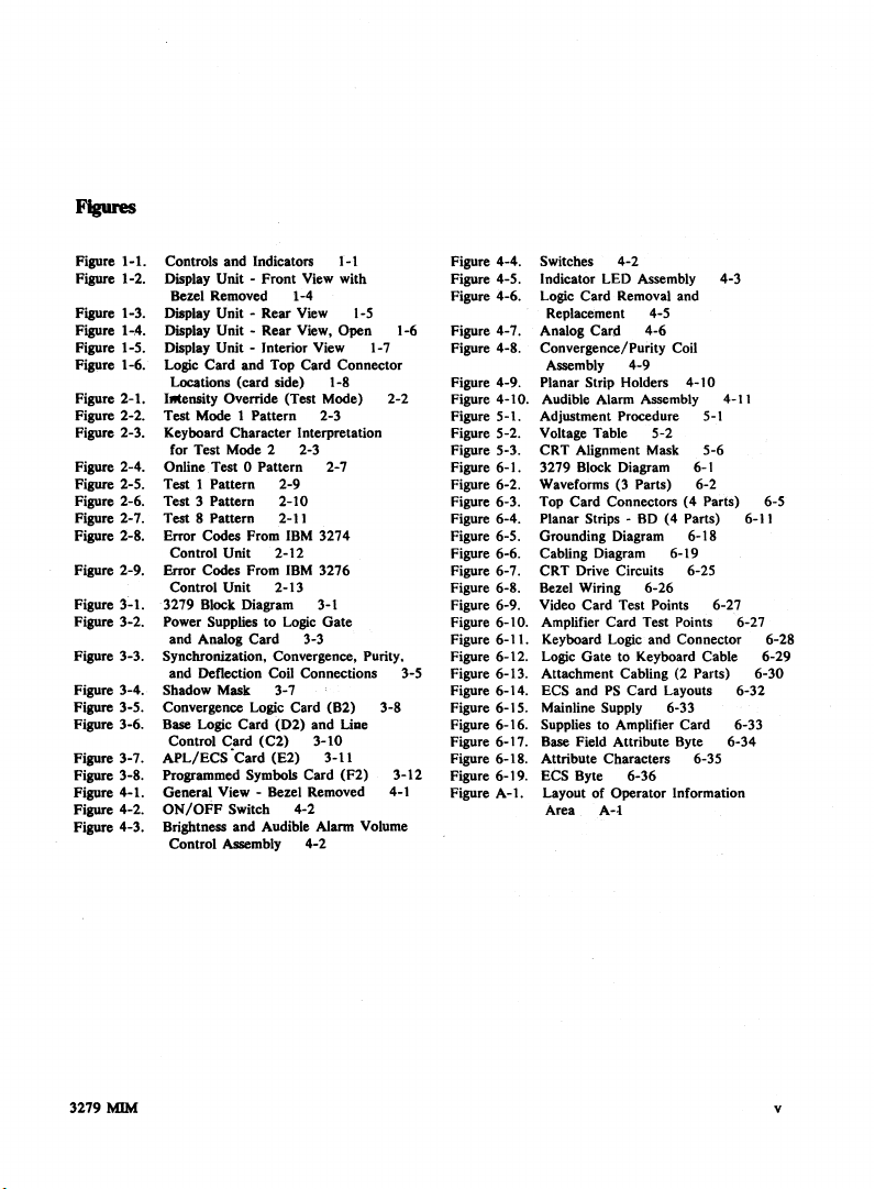
Figure
1-l.
Figure 1-2.
Figure 1-3.
1-4.
Figure
Figure 1-5.
Figure 1-6.
Figure
2-l.
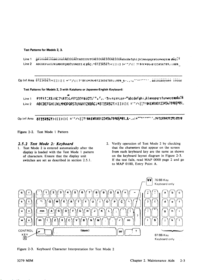
Figure 2-2.
Figure 2-3.
Figure 2-4.
Figure 2-5.
Figure 2-6.
Figure 2-7.
Figure 2-8.
Figure 2-9.
Figure 3-1.
Figure 3-2.
Figure 3-3.
Figure 3-4.
Figure 3-5.
Figure 3-6.
Figure 3-7.
Figure 3-8.
Figure 4-1.
Figure 4-2.
Figure 4-3.
2-10
IBM
IBM
(02)
3274
3276
and
3-10
I-I
Uoe
(F2)
1-5
3-12
Controls and Indicators
Display Unit - Front View with
Bezel Removed 1-4
Display Unit - Rear View
Display Unit - Rear View, Open 1-6
Display Unit - Interior View 1-7
Logic Card and Top Card Connector
Locations (card side) 1-8
Illtensity Override (Test Mode) 2-2
Test Mode 1 Pattern 2-3
Keyboard Character Interpretation
for Test Mode 2 2-3
Online Test
Test 1 Pattern 2-9
Test 3 Pattern
Test 8 Pattern 2-11
Error Codes From
Control Unit 2-12
Error Codes From
Control Unit 2-13
3279 Block Diagram 3-1
Power Supplies to Logic Gate
and Analog Card 3-3
Synchronization, Convergence, Purity.
and Deflection Coil Connections 3-5
Shadow Mask 3-7
Convergence Logic Card (B2) 3-8
Base Logic Card
Control Card
APL/ECS
Programmed
General View - Bezel Removed 4-1
ON/OFF
Brightness and Audible Alarm Volume
Control Assembly 4-2
0 Pattern 2-7
(C2)
'Card (E2) 3-11
Symbols Card
Switch 4-2
Figure 4-4.
Figure 4-5.
Figure 4-6.
Figure 4-7.
Figure 4-8.
Figure 4-9.
4-10.
Figure
Figure 5-1.
Figure 5-2.
Figure 5-3.
Figure 6-1.
Figure 6-2.
Figure 6-3.
Figure 6-4.
Figure 6-5.
Figure 6-6.
Figure 6-7.
Figure 6-8.
Figure 6-9.
Figure
6-10.
Figure 6-I
Figure 6-12.
Figure 6-13.
Figure 6-14.
Figure 6-15.
Figure 6-16.
Figure 6-17.
Figure 6-18.
Figure 6-19.
A-I.
Figure
Switches 4-2
Indicator LED Assembly 4-3
Logic Card Removal and
Replacement 4-5
Analog Card 4-6
Convergence/Purity Coil
Assembly 4-9
Strip Holders 4-10
Planar
Audible Alarm Assembly 4-11
Adjustment Procedure
Voltage Table 5-2
CRT Alignment Mask 5-6
3279 Block Diagram 6-1
Waveforms (3 Parts) 6-2
Top Card Connectors (4 Parts) 6-5
Planar
Strips Grounding Diagram 6-18
Cabling Diagram 6-19
CRT Drive Circuits 6-25
Bezel Wiring 6-26
Video Card Test Points 6-27
Amplifier Card Test Points 6-27
1.
Keyboard Logic and Connector 6-28
Logic Gate to Keyboard Cable 6-29
Attachment Cabling (2 Parts)
and
PS
ECS
Mainline
Supplies to Amplifier Card 6-33
Base Field Attribute Byte 6-34
Attribute Characters 6-35
ECS Byte 6-36
Layout of Operator Information
Area
Card Layouts 6-32
Supply 6-33
A-I
BD
5-1
(4
Parts) 6-11
6-30
3279 MIM
v
Page 7

3279 MIM
Safety
If
with
practice these
with
You
respect
You should take every
possible
pactices
1.
2. Remove all
3.
4. Unplug the
5.
Guidelines
you are aware
electrical and mechanical equipment and
this
need.
You should
conditions or around equipment with
dangerous voltage.
manager
assembling
the immediate area
performing
supplies,
Circuitry.
Power
generators, and other units
Which exceed 30 V ac
be serviced
removed
within the machine, unless maintenance
documentation clearly states otherwise.
(This
grounding is maintained.)
possible
The
be locked in the
a DO NOT OPERATE tag
Be
aware
IBM machine may be
source and be controlled
disconnect
When
equipment having exposed live electrical
circuitry, observe the
a.
Another
controls
(Someone
power
of
the guidelines
guidelines, you can
equipment.
not
fear
it.
and observe the
while
is
wall
it
electricity,
safety
'maintaining IBM equipment:
not
if
this is a potential problem.
power
major
mechanical inspection
or
installing changes
supplies, pumps, blowers,
with
from
done
power
before
box
that a non-IBM
or
is
absolutely necessary
person familiar
must
if it
following
work
alone under hazardous
Always
before removing
components,
of
power
or
power
on when the
its
normal installed position
to
ensure
that
supply
working
switch
circuit breaker.
must
should become necessary.)
on the machine.
when
off
position
(form
powered
by a different
following
be in immediate vicinity.
be there
but
precaution
advise
supplies,
with
42.4 V
proper
cord
turned
or
attachment
with
to
for
working
work
safely
you
must
safety
your
or
working
of
power
in
machine
motor
voltages
dc
must
unit
whenever
off
should
tagged
with
Z229-0237).
to
from
another
to
work
precautions:
power
off
turn
off
vi
b. Do
not
wear
any
jewelry,
frame
eyeglasses,
of
the event
current
contact
c. Use
and appropriate probe
(Remember,
unsafe.)
d. Use only one hand
energized equipment. Keep the
hand in
(Remember there
circuit
procedure helps eliminate a path
in
not
is
an
on
could complete a circuit through you!)
e.
When
that
insulated
used.
f.
Avoid
floor
suitable
necessary.
6.
Follow
working
These instructions are outlined in CEMs and
the
safety
documentation. Use extreme care
checking high voltage.
7.
Avoid
have
not
tools
hand
should be inspected periodically.)
8. Replace
equipment.
-After maintenance, restore all
9.
such as guards, shields, signs, and
leads. Replace
worn
or
are
there
Don't
defeat
them
at
contact, there
flowing
because
area
afforded
only
insulated pliers, screwdrivers,
worn
your
pocket
for
electrical shock. This
using
test
controls are
probes
contacting
strips, machine frames, etc.). use
rubber
mats
special
safety
with
extremely high voltages.
portion
of
use
of
tools
[wire
wrap
or
broken
any
protect
their
purpose
completion
and
been apPllf)ved
worn
.defective. (These
to
the
chains, metallic
or
metal
cuff
links. (In
will
be
of
by
tips/
or
cracked insulation
when
or
behind
must
be a complete
equipment, be certain
set
correctly and
of
proper
ground
purchased locally
instructions
maintenance
test
equipment
by
IBM. (Electrical
guns, drills, etc.]
tools
safety
device
safety
you
from
by
of
the
more
the greater
the metaL)
extenders.
working
on
other
your
that
that
capacity are
potential (metal
when
when
and
test
safety
devices,
ground
that
is
devices
a hazard.
not
replacing
service call.)
is
back.
if
that
Page 8

10.
Safety
glasses
must
be
worn
Using
a hammer
Power
hand drilling.
•
Using spring hooks, attaching springs.
Soldering,
bands.
Parts
cleaning, using solvents, chemicals,
to
wire
cutting, removing steel
when:
drive pins, etc.
and cleaners.
All
other
conditions
hazardous
11.
Never
assume
(Check
it
first.)
Always
12.
your
nongrounded extension cords,
missing safety
13. Do
surface
surface
and can
personal injury.
14. Four
event
a.
be alert
working
not
touch live electrical circuits
of
the plastic dental mirrors. The
of
the dental
result in machine damage and
steps
that
of
an
electrical accident:
USE CAUTION - DON'T
YOURSELF.
b. TURN POWER
c. HAVE SOMEONE
HELP.
d.
ADMINISTER RESCUE BREATHING
VICTIM
IS
15. Do
not
use solvents, cleaners,
have
not
been approved
16.
Lift
by
standing
stronger
leg muscles. This takes strain
back muscles. Do
parts
which
you
17. Each
18. Place removed machine covers in a safe
customer
be certain
renders the
hazards
out-of-the-way
machine. These covers
the machine
to
that
product
to
customer
the customer.
before
which
to
your
eyes.
that
a circuit is deenergized.
to
potential hazards in
environment (i.e.,
grounds,
etc.).
mirror
is conductive
should be taken in the
BE
OFF.
ELSE
GET
NOT BREATHING.
by
IBM.
or
pushing up
not
lift
engineer
action on
unsafe
personnel.
while
the machine
any
is
responsible
his/her
or
must
feel uncomfortable
no
location
might be
damp
floors,
power
surges,
with
A VICTIM
MEDICAL
IF
or
oils
that
with
off
equipment
with.
part
exposes
servicing the
be in place on
is
returned
3279 MIM
to
the
or
19.
Always
place
CE
tool
kit
away
areas
where
no
under
desk
20.
Avoid
caught in machinery.
left
buttoned
Long hair and scarves
21. Ties
clasp (preferably non-conductive)
approximately three inches
when
servicing a machine.
22. Before starting equipment, make sure
fellow
in a hazardous position.
23. Maintain
the machines
completing maintenance.
24.
Avoid
when
lubricating, checking
Prevention
should
always
and practice
Making certain
receptacle meets IBM equipment
requirements.
Inspect line
loose, damaged
Before removing a
retain a charge from the machine, review the
procedure in the maintenance documentation.
CAREFULLY discharge the necessary
components
service procedure.
not
Do
trouble
Never
assume
circuit.
No
time. The exact condition
unknown.
The
power
wired.
Safety
or
defective.
The maintenance and /
may
be uncertain
one can
or
table).
wearing
loose
clothing
Shirt sleeves
or
rolled
up
must
must
be tucked in
CEs
and
customer
good
housekeeping in the area
while
performing and
touching
moving
is the key
good
to
be conscious
cords
electrical safety. You
habits
such as:
that
the customer's
and plugs. Check
or
worn
component
exactly as directed
use
an
ordinary
light.
anything
machine
Here are some
receptacle could be incorrectly
devices
about
is
completely safe a/l
or
features could be missing
or
or
unclear.
from
trip
ovor
it
(i.e.,
that
may be
must
above the
be
secured.
shirt
or
have a
from
the end
personnel are
after
mechanical parts
for
play, etc.
of
electrical safety
power
Pl,lrts.
for
which
by
the
lamp as
an
extension
a machine
of
a machine may be
of
the reasons
modification
elbow.
can
walk
be
tie
that
not
or
of
the
why:
history
of
vii
Page 9
3279 MIM
A
possible
The
machine
transportation
The machine
or
attachment.
An
EC
improperly
The machine
age
or
design
may
damage.
might
or
sales change
installed.
may
environmental
deficiency
have
suffered
have an
may
have
deteriorated
extr8mes.
could
exist.
unsafe
alteration
have been
due
viii
A
component
hazard.
Some
been
Relating
the
condition
to
Before
exercise
caution.
component
incorrectly
to
safety,
of
the
you
begin a service
good
jud!!ment
could
be
of
assembled.
these
machine can
defective,
the
machine
are
and
some
call
proceed
creating
may
of
the
be
affected.
or
procedure,
a
have
ways
with
Electrical
Administering
In
implementing
electrical accident
Use
with
necessary
Power
the
disconnect
dry
pull
with
Act
hel she
possibly
heart
Call
Emergency,
someone
Determine
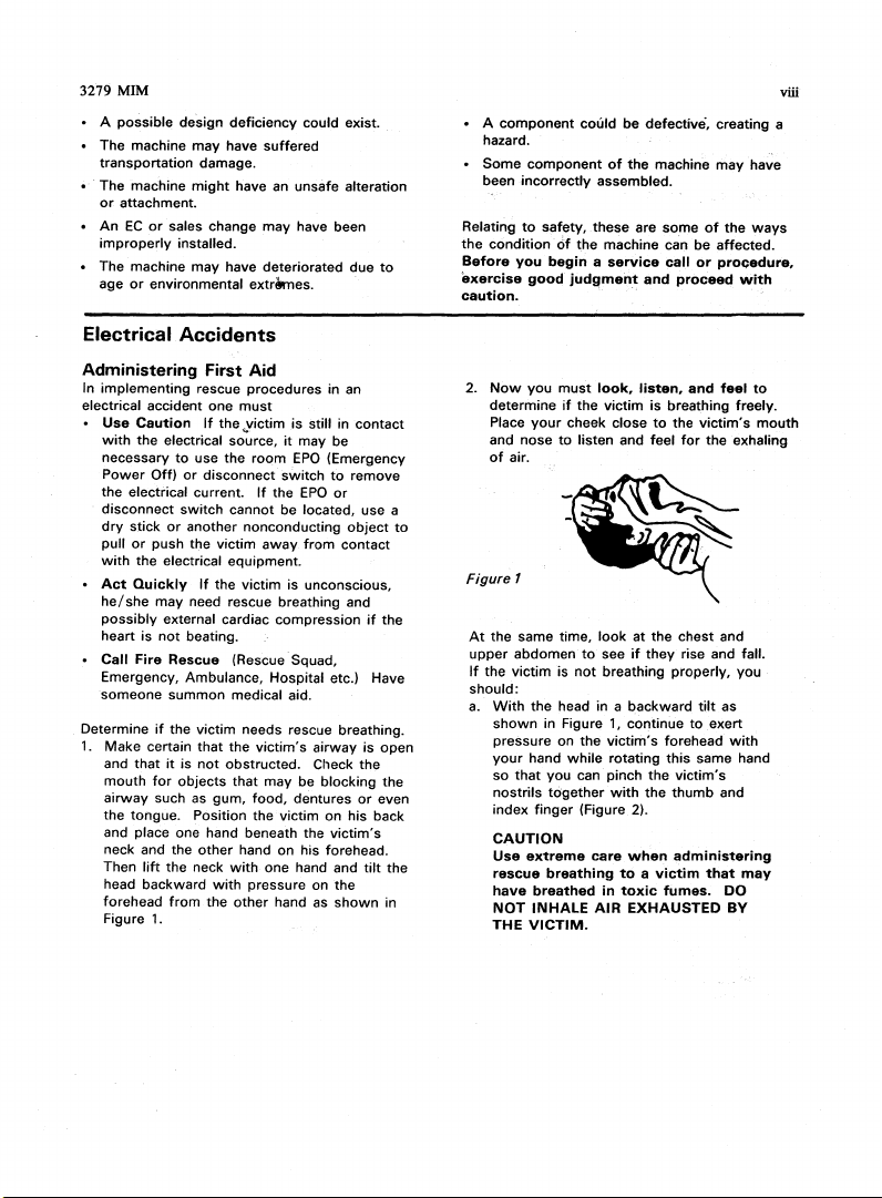
Make
1.
and
mouth
airway
the
and place one hand beneath the
neck
Then
head
forehead
Figure 1.
Accidents
First
rescue
Caution
the electrical
electrical current.
stick
or
the
Quickly
is
Fire
that
tongue.
and the
lift
backward
one
If
the
so~rce,
to
use the
Off)
or
disconnect
switch
cannot
or
another
push
the
victim
electrical
equipment.
If
the
may
need rescue breathing and
external
cardiac
not
beating.
Rescue
(Rescue Squad,
Ambulance,
summon
medical aid.
if
the
victim
certain
that
the
it
is
not
objects
the
from
obstructed.
that
gum,
Position
other
neck
with
with
the
other
for
such as
Aid
procedures
must
victim
room
If
nonconducting
away
victim
needs rescue breathing.
victim's
food,
the
hand
pressure
is
still in
it
may
EPO
switch
the
EPO
be located,
from
is
unconscious,
compression
Hospital
airway
Check
may
be
blocking
dentures
victim
on
his
one
hand and
on
hand as
in an
contact
be
(Emergency
to
remove
or
use
object
contact
if
the
etc.) Have
is
open
the
the
or
even
on
his
back
victim's
forehead.
tilt
the
shown
in
a
the
2.
Now
you
must
look,
listen,
and
feel
determine
Place
and
of
to
Figure
At
the
upper
If
the
should:
a.
With
shown
pressure
your
so
nostrils
index
CAUTION
Use
reSCue
have
NOT
THE
your
nose
air,
1
same
abdomen
victim
the
in Figure
hand
that
you
together
finger
extreme
breathin!!
breathed
INHALE
VICTIM,
if
the
cheek
to
listen
time,
to
is
not
head
in a backward
on
the
while
can
(Figure 2),
care
AIR
victim
close
and feel
look
at
see
if
breathing
1,
continue
victim's
rotating
pinch
with
when
to a victim
in
toxic
EXHAUSTED
is
breathing
to
the
for
the
chest
they
rise and fall,
properly,
forehead
this
the
victim's
the
thumb
administering
fumes,
freely,
victim's
the
exhaling
and
you
tilt
as
to
exert
with
same hand
and
that
may
DO
BY
to
mouth
Page 10
Figure
b. Open
your
breath. Make a
mouth
blow
into the
2
mouth
around the
victim's
wide
tight
victim's
seal
mouth
and take a deep
with
your
mouth
and
(Figure 3).
Figure
4
Figure
3
c.
Remove
your
to
exhale
chest
while
to
fall (Figure
mouth
watching
4).
Cathode Ray Tube
The primary hazard
result·
of
an implosion. The
deal
with
phases are equally
any area could result in
employee
Any
information
unit's
Storage
1.
different
or
additional
CEM/Service
Cathode Ray
received,
from
area
carton,
one
of
sealed
to
of
CRTs
phases
important
customer.
will
of
Cathode Ray Tubes
transported,
to
they
equivalent strength, and securely
prevent accidental opening.
possible
information
be included under
Aids.
Tubes
must
area.
If
must
be in the original carton
and
allow
the
for
the
Safety
is
flying
following
of
CRT SAFETY,
and negligence in
injury
or
variation
that
be enclosed
or
otherwise
they
are shipped in a
victim
victim's
glass
sections
to
an
from
specific
when
moved
Also,
as a
All
this
d. Repeat this cycle once every five
seconds until the victim breathes
himself
or
medical help arrives.
Reporting Accidents
It is
aCE's
accidents, potential electrical hazards, and
miss"
Remember, a linear miss!! accident might be the
result
reporting
resolved quickly.
It's
since the conditions
be varied
2. CRTs should be stacked as per directions on
3.
or
responsibility
accidents
of
a design deficiency and
will
ensure
important
original
and/
carton
protection.
or
be able
should
manufacturer's carton.
with
Cartons should
two
CRT storage areas
flow
pedestrian
be
moisture
to
slightly
or
equivalent packing materials
or
forms
to
give the
piece
of
equipment, the equipment
to
contain the glass fragments
an
implosion occur.
faceplate (viewing surface)
high.
of
material handling equipment and
traffic.
dry
to
insure
and collapse.
to
to
your
field
that
the situation
report
even a
which
to
If
caused
cause serious injury.
must
be placed inside the
tube
proper
tubes
are transported in a unit
When
not
be stacked more than
will
be away
Also, storage areas
that
cartons
for
report all electrical
manager.
minor
prompt
shock
it
need
support
in
doubt,
down.
from
will
not
will
"near
be
only
and
must
stack
normal
must
absorb
3279 MIM
ix
Page 11
3279
MIM
Maintenance and Installation
1.
No one shall be permitted
maintain, replace, or handle high-vacuum
tubes
until
he
has reviewed this CEM.
2. Cathode Ray Tubes
transported,
to
area should be
their original shipping carton and sealed.
3.
When
safety
safety
a.
b. Long-Sleeved Garment.
4.
Tubes
remain
under
5.
Avoid
tube
possibly
6. Prior
discharge all stored potential which
exist
socket
high-voltage
Ray Tubes
both
capacitor.
capacitive
original
discharge
immediately
7. Do
neck alone. The neck is the
the
handle
shipped
be used
placement
container.
or
otherwise
handling CRTs, personnel
equipment at all times. The required
equipment is:
Safety
Glasses - IBM Part 5715010
und<;>r
vacuum
out
of
their
test
or
inspection.
scratching
because
this
cause
it
to
removal
of
on the
tube's
pins and the capacitor
supply. (NOTE: Some Cathode
contain a conductive
the
inside
and
Within
charge
discharge.
each
tube a second
before
not
handle Cathode Ray Tubes
tube
and
is
easily broken.
tubes
with
with a lifting
for
the removal
of a tube
to
install, adjust,
when
received,
moved
completely
carton unless
or
bumping any
may
to
any high-vacuum tube,
anode button
outside
some
builds
It
removal.)
two
enclosed in
will
not
be permitted
weaken
implode.
surfaces
tubes, a
up
following
is
therefore
time
weakest
hands.
strap, this strap should
of a tube
into,
the shipping
from
area
will
wear
they
are
part
of
the glass and
may
or
base
in
the
coating
on
to
form
second
the
important
by
the
part
Always
If
the CRT is
from,
the
and
x
8.
When
inserting
or
equipment,
large end
or
out
of
present, can be used in this process.
9.
Avoid
placing the
when
there
rolling.
If
anywhere except in its special carton, a
of
felt
piece
placed under
glass. Place larger tubes vertically on
faces, and
to
a
to
of
possibility
10.
When
removing a
should be enclosed in
as soon as
of
breaking. Cathode Ray Tubes should be
placed in the carton
up
and the neck
weight
of
neck. The container should be sealed
with
securely
tipping,
turned
positioned
Disanning Cathode Ray Tubes
Field personnel should
Tubes. Tubes
in
accordance with existing Environmental
Protection
return.
Disposal
An
Inventory/Distribution
to
the Branch
disposal
of
July
14, 1980
removing tubes
they
must
while
position. The
is
it
is necessary
not
of
possible
the
face
Agency
of
CRTs.
be supported
carefully guiding
lifting
tubes
any
or
it
rolling.
tube
strong
will
on a table
possibility
to
other
soft
to
prevent scratching the
on their sides,
tube
its
to
reduce the chances
with
down.
Be
is
not
tape
over
so the tube is
down.
not
be disarmed and
requirements at the plant
Cathode Ray Tubes
Office
with
from
by
the
the
neck in
strap,
if
or
bench
of
the
tube
place a
tube
material should be
their
to
prevent the
from
equipment,
shipping container
the large face end
sure
that
resting on the
and,
disarm Cathode Ray
letter
instructions on the
the
to
prevent
disposed
has been issued
it
of
of
Page 12
hand
Chapter
1.
General
Description
and
Locations
1.1 Introduction
The
IBM
3279
by
a coaxial cable
or the IBM
an
Integrated Display Printer
processor.
color display
Four
3B. Model 2 has
Model 3 has
additional model
system-control console. see
Color Display Console Maintenance Information
SY33-0090. Models with an A-suffix
four colors. Models with a B-suffix have
highlighting and 7-color capability
additional font for
Control
B-suffix,
model2A.
Optional features include a selector light pen, a
security keylock, and magnetic reader control (for
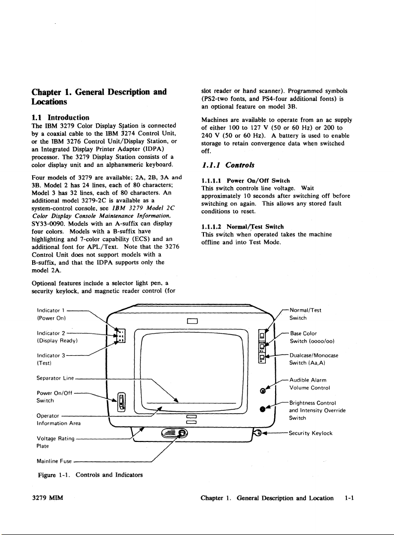
Indicator
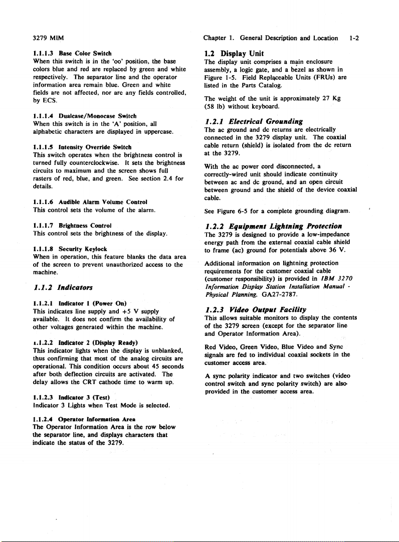
(Power Onl 0 Switch
Indicator
(Display Ready)
Indicator 3 I
ITestl
Color Display Sfation
to
the IBM :1274 Control Unit,
3276
Control
Unit/Display
The
3279
Display Station consists of a
unit
and an alphanumeric keyboard.
models of 3279 are available; 2A, 2B,
24
lines,
32
lines, each of 80 characters.
3279-2C
and
APL/Text.
not
support models with a
that
the
IDPA
Unit does
each
is available as a
'~i
2.~
is
connected
Station, or
Adapter
(IDPA)
3A
characters;
An
Model
display
and
an
the
3276
2C
and
..
of
80
IBM
3279
can
(ECS)
Note
that
supports only the
r-"(-=============-::,
••
slot reader or
(PS2-two fonts, and PS4-four additional fonts)
an
optional feature
Machines are available
of
either
100
240 V (50
storage to retain convergence data when switched
off.
1.1.1
COli
1.1.1.1 Power
This switch controls line voltage. Wait
approximately
switching on again. This allows any stored fault
conditions
1.1.1.2
NormallTest
This switch when' operated takes the machine
and
offline
scanner). Programmed symbols
on
model 3B.
to
127 V
Hz).
operate
(SO
or
A battery
to
or
60
trois
On/Off
Switch
10 seconds after switching off before
to
reset.
Switch
into Test Mode.
iNormal/Test
Q
ea
~
I Switch IAaAI
from an ac supply
60
Hz)
or
200
is
used
to
Base
Color
Switch (oooo/col
Dualcase/Monocase
is
to
enable
:::~:::/~~:----~
Switch
Operator ,
Information
Voltage Rating
Plate
Mainline Fuse
Figure 1-1. Controls
3279
-------!-....
Area
-------
-----------
MIM
I--~-,
-++-----'"
___
\
~~L._______
'--
."
~
.-/
'-"----r-7---::=====;:-=---------r:::--
V,
-r@A)h_securitYKeYIOCk
1...
____
~_:;;.?-:..---------..JJ-
and
Indicators
Chapter
I.
~~~~~~:
.J.---arightness
• ) and Intensity Override
General Description
~~~:Ol
Control
Switch
and
Location
1-1
Page 13
3279
MLM
1.1.1.3
Base Color Switch
is
in the
'00'
When this switch
colors blue and red are replaced by green and white
respectively. The separator line and the operator
information area remain blue. Green and white
fields are not affected, nor arc any fields controlled,
ECS.
by
1.1.1.4
Dualcase/Monocase Switch
When this switch
alphabetic characters are displayed
1.1.1.5 Intensity Override Switch
This switch operates when the brightness control
turned fully counterclockwise. It sets the brightness
circuits to maximum and the screen shows
rasters
of
details.
1.1.1.6
This control sets the volume of the alarm.
1.1.1. 7 Brightness Control
This control sets the brightness of the display.
1.1.1.8
When in operation, this feature blanks the data area
of
the screen
machine.
1.1.2
1.1.2.1 Indicator I (Power On)
This indicates line supply and
available.
other voltages generated within the machine.
1.1.2.2 Indicator 2 (Display Ready)
This indicator lights when the display
thus confirming that most
operational. This condition occurs about 45 seconds
after both deflection circuits are activated. The
delay allows the CRT cathode time to warm up.
1.1.2.3 Indicator 3 (Test)
Indicator 3 Lights when Test Mode
1.1.2.4 Operator Information Area
The Operator Information Area is the row below
the separator line, and displays characters that
indicate the status of the 3279.
is
in the
red, blue, and green. See section 2.4 for
Audible Alarm Volume Control
Security Keylock
to
prevent unauthorized access to the
Indicators
It
does not confirm the availability of
position, the base
'A'
position, all
in
uppercase.
+5
V supply
is
is
selected.
unblanked,
of
the analog circuits are
is
fuU
Chapter
1.
General Description and Location
1.2 Display Unit
The display unit comprises a main enclosure
assembly, a logic gate, and a
Figure 1-5. Field Repl""eable Units (FRUs) are
in
the Parts Catalog.
listed
The weight of the unit
(58 lb) without keyboard.
1.2.1
Electrical Grounding
The ac ground and de returns are electrically
connected in the 3279 display unit. The coaxial
cable return (shield)
at
the 3279.
With the ac power cord disconnected, a
correctly-wired unit should indicate continuity
between ac and de ground, and an open circuit
between ground and the shield of the device coaxial
b~zel
as shown
is
approximately 27
is
isolated from the dc return
in
Kg
cable.
See Figure 6-5 for a complete grounding diagram.
1.2.2
Equipment Lightning Protection
The 3279
energy path from the external coaxial cable shield
to frame (ac) ground for potentials above 36
Additional information on lightning protection
requirements for the customer coaxial cable
This allows suitable monitors to display the contents
of
and Operator Information Area).
Red Video, Green Video. Blue Video and
signals are fed to individual coaxial sockets
customer access area.
is
designed to provide a low-impedance
V.
is
(customer responsibility)
Information Display Station Installation Manual Physical Planning. GA27-2787.
1.2.3
Video Output Facility
provided in
IBM
3270
the 3279 screen (except for the separator line
Sync
in
the
A sync polarity indicator and two switches (video
control switch and sync polarity switch) are
provided in the customer access area.
also-
1-2
Page 14
1.2.3.1 Video Control Stritch
This switch has three positions:
1.
Central position: The monitor receives the same
balance of color signals
2. ENHANCE position: The blue color of the
monitor
is brightened by the addition of a
fifty-percent-green signal.
3.
TEST position: The color signals to the monitor
are internally connected to the 3279 CRT, thus
allowing direct comparison of the two displays
(except for the separator line and Operator
Information Area).
1.2.3.2
Sync Polarity Stritcb
This switch is used to select either positive or
negative sync pulses at the sync output socket.
devices attached at the same time will receive the
same polarity.
1.2.3.3
SIgDaI
This indicator lights when either
Test Indicator
as
the 3279 CRT.
• The synchronizing signal is faulty,
or
• The Video Control Switch is set to TEST.
All
3279MfM
Chapter
1.
General
De8o;riptil>n
and
Location
Page 15
3279 MlM
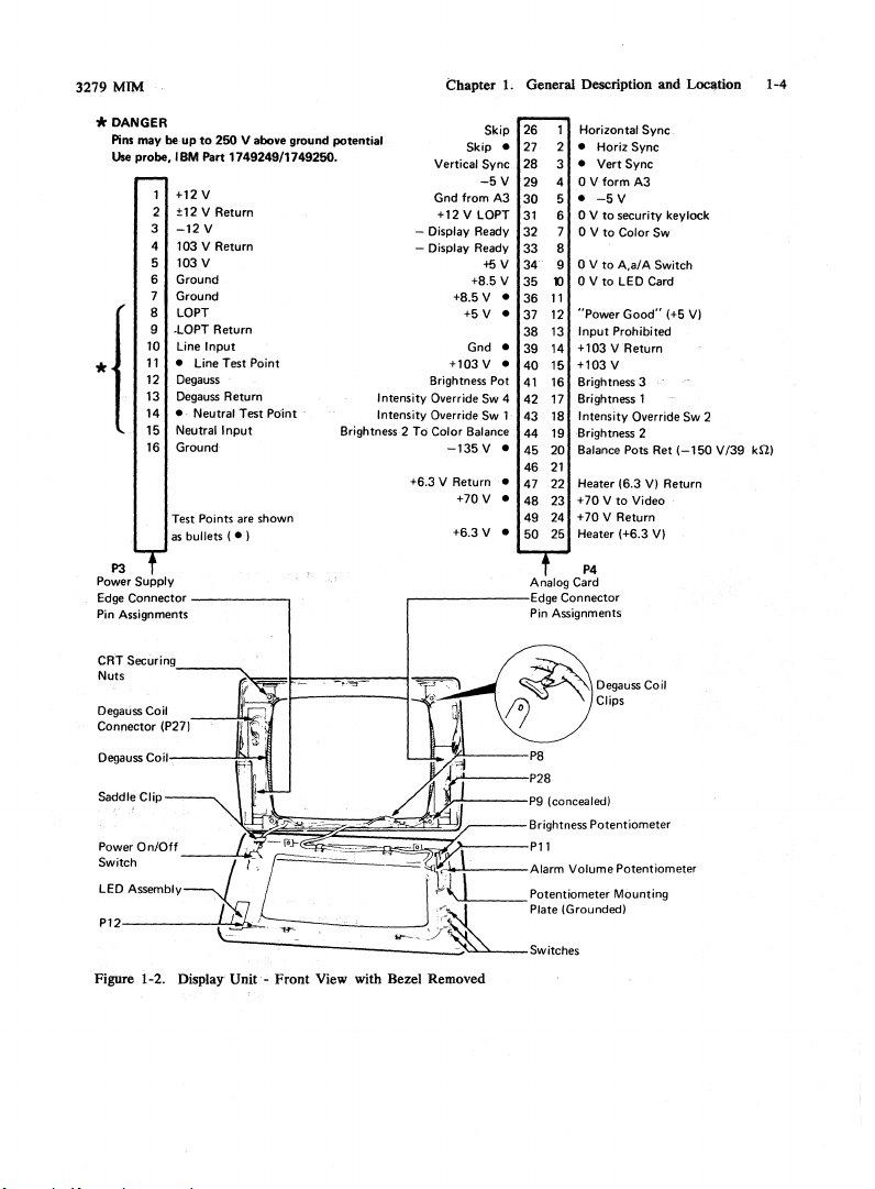
*
DANGER
Pins
Use
*1
P3
Power
Edge
Connector
Pin Assignments
~~~
Securing,
Degauss
may be-up
to
probe,
IBM
Part 1749249/1749250.
+12 V
±12 V Retum
3
-12
V
103 V Return
4
103 V
5
Ground
6
Ground
7
8
LOPT
.lOPT
9
10
Line
Input
Line
11
•
Degauss
12
Degauss Return
13
• - Neutral
14
Neutral
15
Ground
16
Test Points are shown
as
bullets ( • )
Supply
-------,
___
COil
250 V above ground potential
Return
Test
Point
Test
Po-int
Input
---..
Brightness 2 To
Chapter 1. General Description and
Skip
Skip.
Vertical
Sync
-5V
Gnd from
A3
+12 V LOPT
Display Ready
-
- Display Ready
I ntensity Override Sw 4
Intensity Override Sw 1
+6.3 V Return •
+5V
+8.5 V
+8.5 V •
+5 V •
Gnd •
+103 V •
Brightness
Color Balance
-135
V •
+70
V •
+6.3 V •
Pot
26 Horizontal
27
28
29 4
30 5
31
32
33 8
34
35
36
37
38
39 14
40
41
42 17
43
44
45 20
46
47 22
48 23
49
50
Analog Card
Hariz
•
Vert
3
•
o V
form
-5
•
o V
to
6
7
o V
to
9 o V
to
l)
o V
to
11
"Power
12
Input
13
+103 V Return
+103 V
15
Brightness 3
16
Brightness 1
18
Intensity Override
Brightness 2
19
Balance Pots Ret
21
Heater (6.3
+70 V to
+70 V Return
24
Heater (+6.3
25
P4
Edge
Connector
Pin Assignments
V
security key
Color
A,af
LED Card
Prohibited
Sync
Sync
Sync
A3
A
Good"
V)
Video
Sw
Switch
(+5 VI
Return
VI
Loclltion
lock
Sw
2
(-150
V/39
1-4
kUI
P12-----~~~
Figure 1-2. Display Unit -
Front
View with Bezel Removed
Page 16
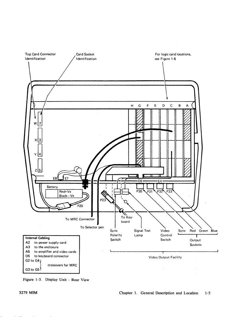
Top
Card Connector
Identification
Card Socket
Identification
For logic card locations,
see Figure 1-6
Internal
Cabling
A2
to
power supply card
A3
to
the
enclosure
to
amplifier and video cards
to
keyboard connector
to
G4f
crossovers for M
to
G5
RC
G2
G3
A5
05
Figure 1-3. Display Unit - Rear View
3279 MIM
Sync
Polarity
Switch
Signal Test
Lamp Control
Chapter
1.
Video
Switch
I
Video
Output
Facility
General
Description and Location 1-5
Sync
,
Red Green
Output
Sockets
Blue
,
Page 17

3279 MIM Chapter
1.
General Description and Location
\-6
Analog Card
,
View
hole
CRT
filament
Jumper
*
**
*
**
**
o HCENT
for
***
Two
Factory
preset (some presets are
Four
Static Convergence Controls
DANGER
Ensure the insulated covers are
transistor
in
these
(1
kV pkl
two
potentials
Amplifier
(J)Q:.~:PURITyA
BLAT0B~}
G0R~
MIN ~ 0
MAX
~
PI?
All
ground
wires
only
on
positions
as
the
Card
o STATIC
4BLAT
GAIN*
Q}COLOR
~
S BALANCE
1011
I
(
In'
\"
~p'4
I'
•
\
1'1'2
L."'.l_
Video Card
(for
Test Points,
see
Figure 6·10)
early
level cards)
in
place on
cases are
Test Points
alpl?S
any
at
dangerous
(see
Figure 6-11) Power Supply Card ***
N
Convergence and Purity
Coil Assembly
Figure
\-4.
Display Unit - Rear View, Open
Page 18
Cathode
Tube
& Coil
Assembly
Bezel
Ray
EHT
Connection
CRT
Label
Main
Enclosure
Assembly
Audible
Alarm
Deflection
Coils
Analog
Card
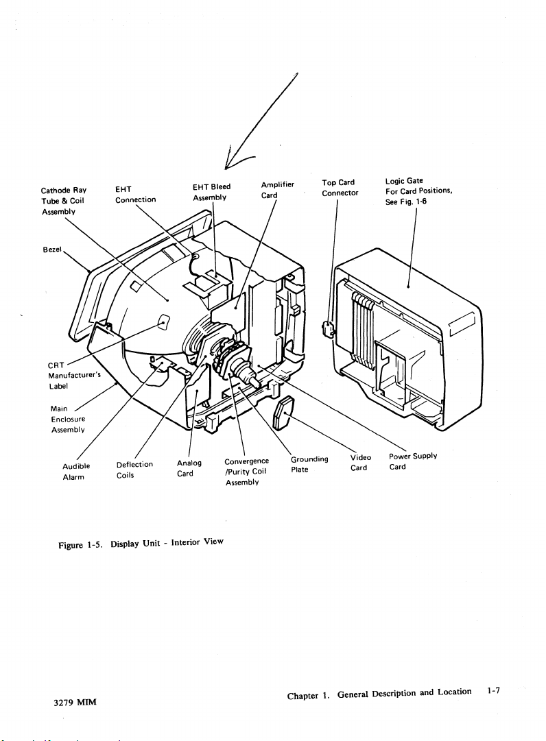
Figure 1-5. Display Unit - Interior View
EHT Bleed
Assembly
Convergence
IPurity Coil
Assembly
Amplifier
Card
Grounding
Plate
Top
Card
Connector
Video
Card
Logic
Power
Card
Gate
Supply
3279
MIM
Chapter
1.
General Description
and
Location
1-7
Page 19
3279
MIM
Chapter
I.
General Description and Location
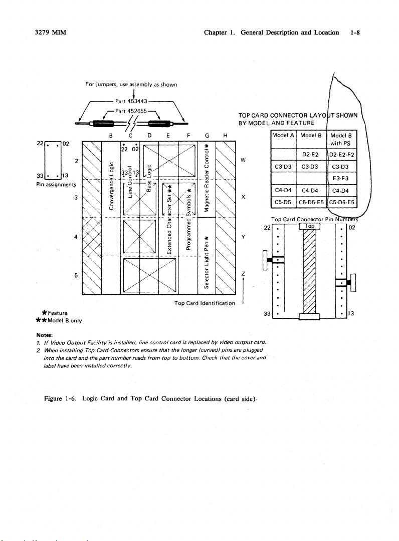
1-8
220'
02
33,
,13
Pin
assignments
For jumpers, use assembly
~
Pon
/ Lpan
..bcSIa:=!
BCD
3
4
as
shown
j
453443:-\
452655~
!==CIIIIa~
.~
.::
~
'"
E F
-+--+---
it
i<
\
~i<
•
"'-
--
"0
.c
~
til
"0
~
~
0
0:
G
i<
~
o
u
~-
a:
u
~
§,
~
i<
c
~
a.
.c
0>
.J
TOP
BY
H
w
x
Y
§ Z
Top
Card
Id:ntlflcatlon
* Feature
** Model B
Notes:
1.
2.
only
If
Video
Output
Facility
is
Mlhen
installing Top Card Connectors ensure
into the card and the part number reads from top to bottom. Check that the cover and
label have been installed correctly.
installed, line
control
card
is
replaced
that
the longer (curved) pins are plugged
J
by
video
output
CARD
MODEL
card.
22
33
CONNECTOR
AND
Model A Model B
C3·D3 C3·D3
C4·D4
C5·D5
~-----L
LA
FEATURE
D2·E2
C4·D4 C4·D4
____
YO
with
D2·E2·F2
C3·D3
E3·F3
i---~-"
PS
Figure 1-6. Logic Card
and
Top Card
Connector
Locations (card side)·
Page 20

1.3 Keyboards
1.3.1
Scan Codes
Pressing a key generates a seven-bit scan code that
is presented serially
code for a specific key position
The control unit translates each scan code into the
appropriate character
1.3.2
Break Codes
Several keys, including the reset key, produce a
second scan code (called a
is released. The break code for the reset key
ignored by
1.3.3
Keyboard Cable
This cable carries the control and data signals
between
the
provides the
Figure 6-12 for details).
1.3.4
System Upshift
System upshift cannot be selected from the
keyboard; it is controlled by the application program
and
applies
is
in upshift mode,
or
IDPA,
Characters
entered by an operator using the override capability.
1.3.5
Keyboard Type Identification
The keyboard logic card contains four pairs
that
must
keyboard (see Figure
1.3.6
Keyboard Lock
The
keyboard can
characters are ignored by the control unit).
data, for example a 'reset'
accepted.
The
operator
change in
clicker normally clicks
but
stops clicking
operator
has chosen
normal operation, then- keyboard lock will cause
to
click at each key depression.
An
)(
is displayed
Area
when
to
the control unit. The scan
is
a1ways
the same.
or
function.
'break
code') as the key
the
control unit.
keyboard
and
+5
V supply for the keyboard (see
to
all keyboard types. When the system
processes only specified characters.
other
be
jumpered
is
made
the
action
the
keyboard
the display unit.
the
control unit
than
those specified may be
to
6-11).
be
'locked'
aware of keyboard lock by a
of
the
once
after
keyboard lock.
to
turn
in
the
is
(3274
indicate the type of
(that
is, keyed
scan
code, may still be
keyboard clicker.
for each key depression,
off
the clicker for
Operator Information
locked.
If
It
or
of
Specific
the
is
also
3276),
pins
The
it
1.3.7
Numeric Lock (Feature)
The numeric lock feature
keyboard jumper in position 1
jumper block. This feature limits the characters
that
can be
entered
o through 9
period
(.)
or comma (,)
(-)
minus
The DUP key remains active. Depression
other key while the cursor
causes
the
keyboard
)(
* NUM in the operator infonnation area.
RESET
Press
1.4 Tools
The following tools and test equipment are required
for maintenance of the 3279.
Item
Insulated probes·
General
Miniprobe**
GLP
Key top puller
Keylock retaining nut wrench
MR
C test card
SLT jumper (3)
SLT
Adjusting tool
Metric tools
Alignment mask
Isopropyl Alcohol
Lint-free
to clear the locked condition.
and
logic probe
extension cable
pins···
cloth
For use with standard
This probe
(up
to
15 volts)
For use with jumpers on some top
card connectors
is
selected by installing a
of
into a numeric field to:
is
in
to
a numeric field
lock with the symbol
Test Equipment
CE
is
for use on low voltage
meter
the keyboard
of
IBM
Part
Number
1749249
and
1749250
453212
453718
453605
9900373
4418787
1742659
452655
453443
1864853
1749235
4423472
2200200
2108930
1D
any
3279
MIM
Chapter
1.
General
Description
and
Location
1-9
Page 21
3279
MIM
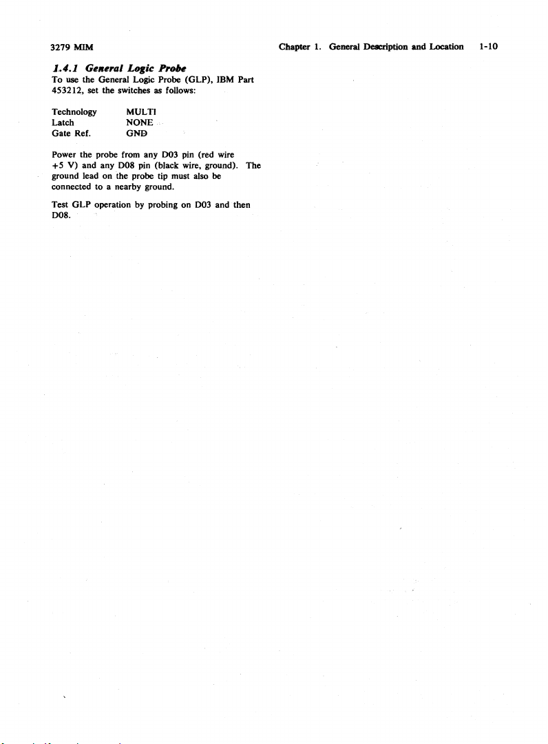
1.4.1
Ge"eral Logic Probe
To use the General Logic Probe (GLP),
453212, set the switches as follows:
Technology
Latch
Gate
Ref.
Power the probe from any D03 pin (red wire
+5
V) and any D08 pin (black wire, ground). The
ground lead
connected to a nearby ground.
Test
GLP
D08.
MULTI
NONE
GND
on
the probe tip must also be
operation by probing on D03 and then
IBM
Chapter 1. General Description
Part
and
Location
1-10
Page 22
Chapter 2. Maintenance
1.1 Maintenance Plan
The maintenance plan for
of:
1.
Problem determination procedures (performed by
the customer using
Guide,
which is located under keyboard
handrest).
2.
The
General Failure Index
QOOO)
for simple symptoms.
3. The Maintenance Analysis Procedures (MAPs)
(referred
2
of
this manual.
4. Intensity override (section 2.4).
5. Offline test modes (section 2.5).
6. Online tests (section 2.6).
7. Adjustment procedures (see Chapter 5).
FRU
removal and replacement (see Chapter 4).
8.
FRU
locations
Catalog
at
DANGER
Do
.."
Iltmltpt
It.
lfItIdti,..
f-
1.1 General Failure Index
This section has been moved to MAP 0000.
1.3
MAPs
This section also has
1.4
Intensity Override
To
engage intensity override, turn and hold
brightness control
override turns
electron-guns
the
to
in section 2.3) which comprise Part
can
be
the back of this manual.
to
...-.It% FR
been
fully
on
the
red, green, and blue
at
maximum brightness.
Aids
the
3279
assumes the use
Problem Determination
(GFI)
(see MAP
found in the Parts
Us
"".,
ptJW#"
OIImM
moved to MAP 0000.
counterclockwise. Intensity
the
When the
three rasters
unless the Test Mode 3 jumper (D2Y08 to D2Y09)
is installed. Test mode checks analog and
associated circuits.
When the
the 3279 is connected to an active control unit, the
red. green, and blue rasters should be converged.
Skip and display geometry can be inspected.
Normal/Test
will
Normal/Test
switch is set to Test, Ihe
be unconverged (see Figure
switch
is
set to Normal
2-1)
and
1.S Test Modes (Offline)
Note: When the display station is offline. the
convergence correction circuits are no/ active. This
will
be obvious when more than one color
displayed.
2.5.1
Test Mode
1. Set the Dualcase/Monocase
A,a.
2. Set the
3. Verify operation of Test Mode 1 by checking
Normal/Test
to Test. The Test Mode 1 pattern
the displayed pattern carefully against the
pattern shown in Figure 2-2.
MAP 0000 page 2 and then go to MAP
read
0100,
Entry Point
1:
Patterll
(A,a/
switch to Normal and back
BB.
is
A) switch to
is
displayed.
If the test fails,
3279
M1M
Chapter
2. Maintenance Aids 2-1
Page 23

3279 MIM
Chapter
2.
Maintenance Aids 2-2
*At
regular intervals across
double
skipline
as a dark
line when converged.
the
appears on Maqel 3. Each
screen on Model 2. Only the
skipline
Figure 2-1. Intensity Override (Test Mode)
appears
Page 24
Test Pattems for Models 2, 3.
Line
1
~e
laUa';
i.ouae
Line 2
iounAEiOUAOY
ABCDEt'~UlJKLMNOPQRSTUVWXYZ
AEEIOUYCA.EIotiAi:i60fi-Ei6uNabcde
A':
~Ac;'e
ii'ig67><l1 ) ()
(='"
/'1:
fghi
jk
7'
lmnopqrstuvwxyz22
$¢£"PtoB
12
3456
~ac;-;;
789"
H@%
OplnfArea
Figure 2-2. Test Mode 1 Pattern
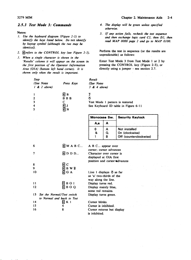
2.5.2
1.
61234567><{})
Test Patterns for Models
Line 1
f·)fft::<~JJ)tJ"I*~:"/H137')I>~O'J:'''·.
Line 2
ABCDEFGHI
Test Mode
Test
Mode 2 is
display is loaded with the Test Mode 1
of characters. Ensure
switches are set as described in section 2.5.1.
(}
(='"/\I:?I$¢£¥Pt<le123456789~~t@,_&-.,q-'-o,,"'-··",
2,
3 with Katakana or Japanese-English Keyboard:
-
JKLMNOPQRSTUVWXYZli0flCi
2:
Keyboard
entered
automatically
that
the display unit
after
pattern
the
~elou~oy~e~
r
J,
"7<
?IH
13,-"abcdefgh I
*012345b7)
( (1) () ( =
2. Verify operation of Test Mode 2 by
that
the characters
from each keyboard key are the same as shown
on the keyboard layout diagram in Figure 2-3.
If the test fails, read MAP
to
MAP 0100, Entry Point A.
Jklmnop~rs\uvwxyza.kii
".
/\1:
?ISU¥P.1I01Z3451078'11l§'@%-
that
appear
!i¥\
U
on
0000
page 2
76/BB·Key
Keyboard
lOUUC
checking
the screen
and
only
go
Figure 2-3. Keyboard
3279
MIM
Character
Interpretation for Test Mode 2
Chapter
2. Maintenance Aids 2-3
Page 25
3279
MIM
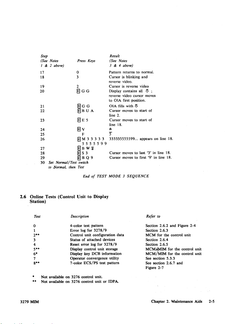
2.5.3
Test Mode
Notes:
1.
Use
the keyboard diagram (Figure 2-3) to
identify the keys listed below.
by
key
top symbol (although the
identical).
2.
I9refers to the
3. When a single character
'Results' cl!/umn it will appear
the first
(OIA) (bol/om left hand corner). It
Area
shown only
4
6
8
9
10
11
12
13 Set the Normal/Test switch
14
15
16
J:
Commands
CONTROL
pOSition
of
the Operator Information
when
the
r~sult
Step
(See Notes
1
& 2 above)
I
2
3
to Normal and bock to
Do
two
key
(see
is
shown
on
is important.
Press Keys
I9B
BBB
C
@lJ
@IN
19
M
19
DO
I9c
@lBW;
@lGA
@I
B 0 I
@lBOQ
@I
K I
4
8
not identify
may be
Figure 2-3).
in
the
the screen in
is
ABC
...
D ...
Test
Chapter 2. Maintenance Aids
4.
The display will
otherwise.
5.
If
any action fails, recheck the test sequence
and the
MAP
read
Perform the test in sequence (or the results are
unpredictable)
Enter
Test Mode 3 from Test Mode I
pressing the
directly using a jumper - see section 2.7.
Result
(See Notes
3 & 4 above)
2
6
Test Mode 1
See Keyboard
Monocasa
ABC
cursor; cursor advances
Character over cursor is
displayed
position and cursor
Line I displays
as
'a'
way along the line.
Display turns red.
Display mainly blue,
some red remains.
Display turns green.
Cursor blinks.
Cursor
Cursor returns but display
is
inhibited.
pattern
ID
Sw_
A,a A
0 A
a.
&
1 B
... appear over
at
OIA first
two-thirds
is inhibited.
table in Figure 6-11
<5
of
be
green unless specified
.. exchange logic card C2, then D2, then
0000' page 2 and go to MA.P 0100.
as
follows:
CONTROL key (Figure 2-3),
is restored
Sacurity
Kaylock
Not
installed
On
(clockwise)
Off
(counterclockwise)
.dvances
as far
the
or
2 by
or
2-4
Page 26
Step
(See Notes
I & 2 above)
17
18
19
20
21
22
23
24
25 F
26
27
28
29
30
Set Normal/Test switch
to
-1!Iormal,
then
Press Keys
o
2
@lGG
@lGG
@lBVA
@lE5
@lv
@lM
@lB
@l
19
Test
3 3 3 3 3
5555599
W
iii
S 3
B Q 9
End
of
Result
Notes
(See
3 & 4 above)
Pattern returns to normal.
Cursor
is
blinking
reverse video.
is
reverse video
Cursor
Display contains all
reverse video cursor moves
to
OIA
first position.
OIA
fills with
Cursor moves to start of
line 2.
CUTsor
moves to start
line 18.
A
5
333335555599
CUTsor
moves to last '3'
Cursor moves
TEST
MODE 3
SEQUENCE
and
(5
<5
of
... appears
to
on
in
first '9' in line 18.
line 18.
line 18.
2.6 Online Tests (Control Unit
Station)
Description
4-color
Error
log for
Control
Status of
Reset error log for
Display control unit storage
Display key
Operator
7-color
on
3276
control unit.
on
3276
control unit or IDPA.
3219
Test
o
2"
3
4
5··
6·
7
8··
MIM
Not
Not
available
available
to
Display
test
pattern
3278/9
unit configuration
attached
devices
3278/9
DCB
information
convergence utility
ECS/PS
test
pattern
data
Refer
10
Section 2.6.2
Section 2.6.3
MCM
Section 2.6.4
Section 2.6.5
MCMfoMIM for
MCMiMIM
See section 5.3.3
See section 2.6.7
Figure
Chapter
and
for the control unit
for the control unit
2-7
2.
Figure
2-4
the
control unit
and
Maintenance Aids 2-5
Page 27
3279
MIM
2.6.1
Running Online Tests
I.
If the
'READY'
symbol
is
OIA, set the
back to Normal.
2.
Hold down the ALT key, press the TEST key,
and release both keys.
OIA.
3. Key in
number,
reported upon, and n
Notes:
a.
b.
c.
Normal/Test
pp/
n and press ENTER. (pp
0-31,
of
~
If
pfJ
is omitted the test
requesting terminal.
The / must always be keyed in.
If
n
is
omitted, test 0
not displayed in the
switch to Test and
TEST appears
the device to be tested
is
the number
is
is
run on the
run.
in
is
of
the
the
port
or
tile test.)
4. To end the online tests:
ALT
Hold down the
key, and release both keys. TEST
disappears from the OIA.
key, press the TEST
5. Error Indicators. (Press RESET to continue.)
)C
-f
(Do
a.
... you tried to select an in-session terminal
for
b.
)C
number) ...
or
test format
slash / and no spaces).
Note:
an IDPA.
2.6.2
2.6.2.1 Routines Only
The IBM 3276 control unit precedes the main test
with two transmission test routines.
Note: Before going
read the danger notice at the start
not enter, Function not available)
Test
O.
*.#? (Do not enter,
yOll
address,
)C
used an invalid test number,
or
wrong test format. (Begin
at
position 0
c-f will appear instead
Test 0
for
IBM
3276
Terminals Connected to
Controller
to
a specific
Op
check, What
and
use only
if
MAP
of
MAP
connected
reference,
0000.
one
Test 0 - Routine 1 (3276 only)
This routine 'verifies the basic
Adapter) card functions
command decode, and so on. Driver/Receiver
TA
(Terminal
- register, SERDES,
operations are not tested.
the test stops.
Display Station Maintenance Information
Manual,
Test 0 - Routine 2 (3276 only)
This routine
communications link
receiving a
the
test stops.
to MAP
2.6.2.2 Four-color
This test is used to verify
The correct control
attribute byte.
3279
The
The interaction
or
IDPA.
The action of the
To
run
test 0, see section 2.6.1.
J. Ensure the
2. The alarm sounds when one
Figare 2-4 appears.
3. Verify
white
and
changed to
If
to
this test fails read MAP
to Map
the
4. Reset
5. The
pattern
port number pp.
Chapter 2. Maintenance Aids
See
If
IBM
3276 Control Unit
SYlS-2oo4.
is
the
Link
test.
by
POR
0100,
issuing reset
response.
Read
MAP
Entry
Point CC.
Pattern
Test
the
of
a field by the field
0000
following:
alarm.
of
the 3279 with the control unit
0000/00
switch.
0000/00
switch is set to
that
the red
and
green when the
00.
0500
entry point A.
0000/00
appears
blue fields become
0000/00
0000
switch to
on
the device connected to
an
eITor occurs,
It
verifies the
and
If
an error occurs,
page 2
0000
of
the patterns
switch is
page 2, and go
0000.
and
•
2-6
go
in
Page 28
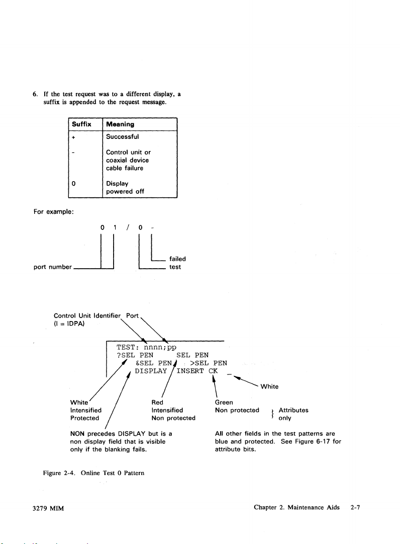
6.
If
the
test request was to a different display, a
suffix
is
For example:
Control
(I
= IDPA)
appended to
Suffix Meaning
+
-
0
Unit
the
Successful
Control
coaxial device
cable failure
Display
powered
Identifier
I/,
/
/
White
IntensIfIed
Protected
NON precedes DISPLAY
non
display
only
field
if
the blanking fails.
request message.
unit
or
off
o
I L failed
~test
Port
TEST:
nnnn;pp
?SEL
that
PEN
&SEL
DISPLAj
is visible
SEL
P'~I
Red Green
Intensified
Non
but
INSERT
protected
is
a
>SEL
PEN
PEN
C\
-~
Non
protected t Attributes
All
other
fields
blue and
protected.
attribute
bits.
White
f
only
in
the
See Figure 6-17
test
patterns are
for
Figure 2-4. Online Test 0 Pattern
3279
MIM
Chapter 2. Maintenance Aids 2-7
Page 29
3279 MIM Chapter 2. Maintenance Aids 2-8
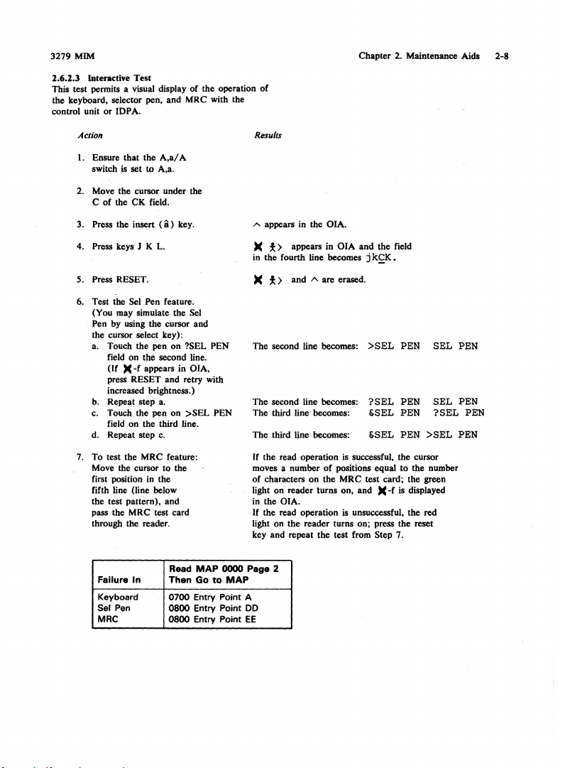
Interactive Test
2.6.2.3
This test permits a visual display of the operation of
the keyboard, selector pen. and
control unit or
IDPA.
Action
1. Ensure that the
2. Move the cursor under the
3.
4.
5.
6.
7.
is
set to A.a.
switch
C of the CK field.
Press the insert
Press keys J K
Press RESET.
Test the Sel Pen feature.
(You may simulate the Sel
Pen by using the cursor and
the cursor select key):
a. Touch the pen
field on the second line.
(If
)(
-f
press RESET and retry with
increased brightness.)
b. Repeat step
c. Touch the pen
field on the third line.
d. Repeat step
To test the MRC feature:
Move the cursor to the
first position in the
fifth line (line below
the test pattern), and
pass the MRC test card
through the reader.
MR
C with the
A,a/
A
(II)
key.
L.
on
?SEL PEN
appears in OIA,
a.
on
>SEL
c.
Results
A appears in the OIA.
)(
* > appears in OIA
in the fourth line becomes
)(
* > and A are erased.
The second line becomes:
The second line becomes:
PEN
The third line becomes: &SEL
The third line becomes: &SEL
If the read operation
moves a number of positions equal to the number
of characters
light on reader turns on, and
in
the OIA.
If
the read operation
light on the reader turns on; press the reset
key and repeat the test from Step 7.
on
and
j
>SEL
?SEL
is
successfUl, the cursor
the MRC test card; the green
is
unsuccessful, the red
the field
k£K
)(
-f
•
is
PEN
PEN
PEN
PEN
SEL
SEL
?SEL
>SEL
displayed
PEN
PEN
PEN
PEN
Failure In
Keyboard
Sel
Pen
MRC
Read
MAP
0000 Page 2
Then Go to
0700 Entry Point A
0800
0800
MAP
Entry Point
Entry Point
DO
EE
Page 30
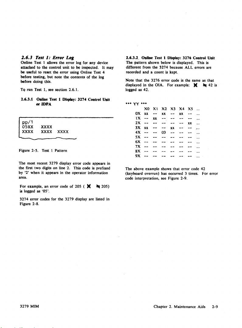
2.6.3 Test 1: Error Log
Online Test 1 allows the error log for any device
attached
to
be useful to reset the error using Online Test 4
before testing, but note the contents of the log
before doing this.
TQ
2.6.3.1 Oaline Test 1 DIsplay:
pp/1
05XX
XXXX
Figure 2-5. Test 1 Pattern
The most recent 32 79 display error code appears in
the first two digits
by
area.
For
is logged as '05'.
3274 error codes for the 3279 display are listed in
Figure 2-8.
the control unit to be inspected. It may
run Test I, see section 2.6.1.
3274
205
Control
()(
or
mBA
XXXX
XXXX
XXXX
on
'2'
when it appears in the operator information
example, an error code
line 2. This code is prefixed
of
~
UDit
205)
2.6.3.2. OnIIoe Test 1 Display: 3276 Control Unit
The pattern shown below is displayed. This
different from the 3274 because
recorded and a count is kept.
Note that the 3276 error code is the same as that
displayed in the OIA. For example:
logged as 42.
•••
yy
•••
Xl
XO
xx
xx
xx
X2
xx xx
03
OX
IX
2X
3X
4X
5X
6X
7X
8X
9X
The above example shows that error code 42
(keyboard overrun) has occurred 3 times. For error
code interpretation, see Figure 2-9.
X3
xx
ALL
X4
)(
X5
xx
is
errors are
~ 42
is
3279 MIM
Chapter
2.
Maintenance Aids
2-9
Page 31

3279 MIM
1.6.4
Test
3:
Status
Summary
Chapter
2. Maintenance Aids
1-10
01234567
11101-11.
DPS C DD
~
XXXX
Notes:
Line 2 symbols
1
Attached
TA
detected
a
No
is
Figure 2-6. Test 3 Pattern
Test 3 gives
to the control
To run Test 3, see section 2.6.1.
1.6.5
Test
Test 4 resets the error log. Its operation can be
verified with tcst
the Reset operation was successful.
To run Test
1.6.6
Test 7: Operator Convergence
Utility.
See section 5.3.3 to use this test.
refer
device
card
failed,
or
error.
T A
card
is
attached
installed,
to
this
data
about each display unit attached
unit/IOPA.
4:
Error
1.
A'
4,
see section 2.6.
....
.
.. ..
.•...
XXXX
XXXX
to
line 1 port
has
device
port.
Log
power
or
Reset
on.
is
disabled
the
numbers
device
+' response indicates
I.
-------
-
..
------
XXXX
because
has
that
as
follows:
power
Configured
See
Note,
D = Display
P =
Console
I
S =
System
C =
1052
Blank =
---
of
control
off,
or
1.6.7
To
run Test 8, see section 2.6.1. The
in Figure
Extended
If
not
OIA
If Test 8 fails, read
MAP
Not
The
last
line
error
summary
documentation).
unit/IDPA
no
device
Test
8:
Symbols
2-7
is
Character
installed, the symbol
and
the test will not run.
0800,
Entry Point
Port
printer,
printer,
Console
connected
may
7-Color
(PS)
displayed.
MAP
Numbers
for
example
for
example
Printer
contain
counts
(see
and
Set (Models 2A
)(
* #? appears in the
0000
page 2
Cc.
3287
3289
control
unit
Programmed
pattern
shown
and
3A)
and
go
is
to
Page 32

Une
1
(~'#,J
5
8
10
11
12
rmD
~:~~:~,~2
PS
<;:()~()~
if
~A
~A
iB
~B
~B
2 3
2 3
~A
~B
~A
~c
~c
~D
~D
4 5
4 5
~E
~E
Une
3
iFl \ ~ are
5 (C) ~ are
6
7 7 (F) P
6
7 8
(C) ~ 5
10
11
12
Notes:
1.
If
PS
fonts
rep/aced
lines
10,
2.
Feature PS2 gives fonts A and
gives 4 extra fonts, C through
3.
Color
is
(C)
Character
Attribute.
AND
IC)
& TEST
IF)
with
white
is
red, 3
is
yellow, 7 is
font
A
font
B (skip supressed)
font
A
installed, the
or
(F)
are reserve video
centers
pink, 4 is
omitted
B.
F.
Extended Field
PS
IC)
& COLOR IF) blink
red
red
is
blue, 2
is
turquoise, 6 is
~
is
red
from
~
is
red
from
~js
red
from
are
not
by
green period and
11
and
12.
green unless stated. Control
Attribute
green
white
~ & ~
is
on
Feature
PS4
is
by
Figure 2-7. Test 8
2.6.8
Error Codes
Try
to
reset
key
or
by setting
then
back
recurs, consult the appropriate table below.
In
the
following error code tables, FRUs are listed
in
order
of probability
following before exchanging any
Seating
• Dirty
or
connector contacts.
Voltages
3279
MIM
Pattern
the
error by either pressing the RESET
the
to
Normal.
of cards
bent
on
Normal/Test
If
of
and
board pins
board pins.
cables.
switch to Test
the failure persists,
failure. Check the
FRU:
or
card/top
card
or
See Figures 6-4 and 3-2 for voltage pin locations
and
section 5. t for voltage tolerances.
Exchange or repair suspected
and verify correct operation each time.
suggested actions do
investigate seating
cables and board wiring, then read MAP
and
go
2
to
MAP
and
0100
FRUs one
not
cure
the
Entry
Point
problem,
A.
continuity of associated
at
If
0000
a time,
the
Chapter 2. Maintenance Aids 2-11
page
Page 33

3279
MIM
Chapter
2.
Maintenance Aids 2-12
3274
Code
202
203
204
205 *
206
207 *
208
209
210 * Keyboard
211
212
222
223
224
225
226
227
228
229 82,
234
295
299
2%%
2EE
* Do
Check
Note:
Figure 2-8.
Repair
(3279
02.
02,
02,
02,
02,
02,
02,
02,
then cable, then
02,
*
Keyboard logic,
*
then
G4, (selector pen),
then
E2,
G2
E2,
E2,
E2,
82, then 02, then
E2.
02,
02,
}
the
control unit and the customization
ECS
card switches,
For
other error codes,
Error
Action
logic
card)
then features then
or
C2.
then
C2,
then features. Unsupported feature attached
then B2, then features. Incorrect feature response
then
C2.
then
C2.
then
C2.
10
jumpers,
then features. Invalid status received
cable; then 02.
02,
then
then
02.
(MRC), then 02.
then
02.
then
02.
then
02.
or
02,
or
then
C2.
then
C2.
Codes
From
B2.
02.
C2.
C2.
C2.
PS
jumper, and keyboard jumpers (see Figure 6-14).
see
control
IBM
3274 Control
Error
Code
Control
unit
buffer
overflow
Feature Bus
Storage
error
on
initialization
Lost
Operation Complete
Invalid (unexpected) Operation
Complete
Command queue failure
Invalid keyboard attached
(not configured)
Invalid scan code received
Invalid selector pen status
or
command queue failure
ECS
buffer
Invalid MRC status
command queue failure
ECS
status/initialization failure
ECS
command queue failure
ECS
write
queue failure
Storage
parity
Storage
parity
Switches
not
Invalid
type
Non-command queue cycle
sharing machine check
Not
customized
support
the 3279 features?
unit
or installed
RPQ
Unit
Explanation
keystroke/status
error
(Device Check)
parity
error
or
alternate command
error
error
set
to
include APL
A adapter status
for
attached features
documentation.
this
display
Page 34

Repair
3276
Code
41
42
43 G2 (MRC), then
44
45
55
56
60
61
70
71
72
73·
74
77
78
Action
(3279
logic
card)
Keyboard logic, then
cable, then
Keyboard logic, then 02.
G4 (selector pen), then
02,
then
C2.
G2 (MRC), then
82
then
02,
82
G2 (MRC), then
G4 (selector pen), then
02,
C2,
C2,
C2, then
02.
02,
02,
02,
then
then
02,
then
then
C2.
then coaxial cable, then
then coaxial then 02. Adapter receive parity error
02.
then features. Feature timeout
then
C2.
then
C2.
02.
02.
02.
02.
C2.
C2.
Error
Code
Explanation
Invalid scan code received
Keyboard overrun
MRC data parity
Selector pen data parity
No response
Storage parity
Storage parity
MRC timeout
Selector pen timeout
02.
No
response
Data parity
Lost Operation Complete this display
Device check
POR
signal
error
from
MRC
error
error
from
terminal (timeout)
error
(buffer
error
parity)
error
• Do the control
Check
Note:
For
Figure 2-9. Error
1.7 Jumper Positions
A number
d!splay adjustments
MIM
3279
unit
ECS
card switches, and keyboard jumpers (see Figure 6-14).
other error codes,
Codes
of
jumper positions
and
and its features support the 3279 features?
see
control
unit
From
IBM
are
fault-finding.
available to
or installed
3276 Control
aid
Unit
RPQ
documentation.
Chapter
2.
Maintenance Aids 2-13
Page 35

3279
MIM
The
positions and their uses are listed below. Note
that
every jumper position is activated when
grounded. A recommended ground pin is listed.
Chapter 2. Maintenance Aids
2-14
Name
Force White
Color Balance Bars
Reverse Video
CE
Jumper
Pen Detect Lines
Power
Storage
Force Characters
Disable Skip
Force Green
Force Blue
Force Red
Pin Ground
C2W07'
C2W28
C2W09" C2W28
D2Y02'
D2Z04
or
E2Z04
D2Y09" D2Y08
D2YlO'
D2Y08
B2B08 B2D08
C2G06
C2J04
D2108
D2J08
C2S11 C2U08
C2S12
C2U08
C2U11 C2U08
Use/Description
All characters
Good test
screen, used to
(at
A number
high, are displayed (must be characters
on
All characters are reversed.
check purity.
When the
Test position, this jumper allows
directly
the
attributes are blank,
are interchanged.
of
screen center).
of
screen). Color balance.
Normal/Test
to
Test Mode 3 without resetting
refresh buffer. Nulls display,
])isplays selector pen detect lines.
Removes power from
convergence check. Used in setting
convergence.
Easy method
characters when online to check overall
convergence.
Inter-row skip (Mod 2 only) is disabled.
Separator line moves
adjusting image height.
Green video
Used to check green video amplifier
gun.
Blue video is forced permanently on.
to check blue video amplifier and gun.
Red video is forced permanently on.
to check red video amplifier and gun.
"See Figures 1-6 and 6-3 for top card connector pin numbering.
on
the screen become white.
convergence over whole
set
up static convergence
colored bars, 2 characters
Used to
switch is set
entry
and
red
and
white
storage
to
force a
of
filling screen with
up.
Used when
is
forced permanently on.
to
up
and
Used
Used
the
Page 36

Chapter
3. Functional
Components
LCC
BLC
Input!
Output
SEROES
Control
Logic
F81l
FBO
C2
02
Convergence
Logic
B2
LCC
BLC
LCC
Clocks
Refresh
Storage
Character
Generator
Color
Control
Video
Outputs
C2
02
02
C2
Video
Output
FacilitY
*Optional
Figure 3-1. 3279 Block Diagram
3279 MIM
MSR/MHS
Power
Supply
Card
Chapter 3. Functional Components
3.1
Page 37

3279 MIM
3.1 Power Supply
The power supply switches the line voltage at high
frequency using pulse width modulation.
The modulated voltagc
windings of a power transformer. The outputs from
the secondary windings are rectified to produce the
following voltages:
Voltage Tolerance Max. Ripple
(V
de)
+103
+12
-12
+8.5
+5
-5 10 0.15
The transformer incorporates a feedback winding to
control the pulse width and hence the output
voltages.
A signal from the analog card (LOPT sense) locks
the power supply oscillator to lhe line timebase
frequency, to eliminate interference on the display
caused by the high frequency modulation. This
signal also indicates to the power supply an
overvoltage condition on the analog card.
If
either the overvoltage or the overcurrent
protection mechanism shuts down the power supply,
up to seven times, approximately once per
it retries
second and the
flashes at this rate, provided that the failure
on
the
+5
V line. An audible click may
the supply at each retry by listening near the
from
ventilation slots above
is
located
A fuse
fails, the power supply card must
is
fed to the primary
(±%)
6 0.7
10 0.4
10 0.4
10
10
'POWER
on
(V
0.26
0.15
GOO~'
the
power supply card.
the power supply card.
pk-pk)
indicator light 1
is
be
heard
exchanged.
If
be
not
it
Chapter 3. Functional Components
3.2 Analog Card
The analog
drives for the CRT scan coils and includes the
extra-high-voltage
logic
synchronizing signals, the time bases on the analog
card lock to the imposed frequency.
The line output transformer
horizontal drive circuit. provides the following
card
generates horizontal
(EHT)
is
supplying horizontal and vertical
power "'pply. When the
(LOPT).
and
in
vertical
the
supplies:
Voltage
(V
de)
+25
-25
+12
+70
-150
+280
to
+6
kV
+6.3
+25
kV
The analog card receives a further signal ('skip'),
which forces the raster to move vertically a defined
amount (see Figure 2-1).
To
start up, the analog card requires ±S V dc,
+8.5
V dc, and + 103 V
turned
on
produces the additional supplies. These enable the
vertical drive circuit to start and this initiates a
delay. After
(indicator
voltage unblanks the screen.
Where Used
- On-card use, deflection
amplifiers
- On-card use, deflection
amplifiers
- On-card use and card B2
- To video card
- Through brightness control,
amplifier card, and color
balance controls to CRT grid
- Focus circuits and CRT anode
+450
- Focus circuits
- CRT filament (see Figure 6-7)
- EHT supply to CRT
the horizontal drive circuit
45 seconds DISPLAY READY
2)
turns
dc.When
on
and a change in CRT grid
the power
starts
and
is
3-2
Page 38

LOPT
-
LOPT
-:-.0
Retur
n
See Figure
Power Supply Card
9 8 S 4
*
*
(
P3
I-r--
IS
..
~+103
1++103
-::-
-
14
[~8
~
Sense
(0
HI
Analog Card
6·4
for
voltage pins on Planar strips
V
V dc return
P4
340
290
30v
3SV
de
+S
-S
+8.5 V
+S V de
A2D03 - A3D03
-5 V de
A2B06 - A3B06 are each connected
o V
de
A3DOB - A3DOB
+8.SVdeA2Bll
d..
+S
V
-S
V
~
OV
+8.SV
A3
===
~
V
V
OV
'---
AS
rD
To
Video
Card
and
Amplifier
Card
*DANGER
Pins may be
-A3Bll
up
82
-
I"'
fo--+-
......
I
~
I
I
I
I
I
~
I
I
I
-
--
I
I I
.....l.-
Logic Gate: Card Side
to
250
V above ground potential
-S
V and
+8.S
through logic card
B2
only.
C2
r---
D2
-
u...
1---1-
r-
~
r---+-
I-----
~
_.1-
---
I
~
-2-
V
-'"
t-
I
I~
I
I
I
I
I
I
I
I
I
I
I
Ve
rtical
Co
nnections
de
Ma
Lo
gic Cards
by
Figqre 3-2. Power Supplies to Logic Gate and Analog Card
3279
MIM
Chapter 3. Functional Components 3-3
Page 39

3279 MIM
3.3 Amplifier Card and Inputs
3.3.1
Conpergence Circuits
The convergence amplifiers drive the convergence
coils. which provide the necessary correction for all
points on the
3-3).
The current in the convergence coils
by data in a store which
scanning of the screen. The data
be altered by
ageing.
As
data
lost when power is turned off. the convergence
store
When the 3279 display
convergence logic card
reset' to the logic. This resets most registers and
sets the status to 'power on reset'. The next poll
from the control unit to which the 3279
connected detects the status and then reada the
SCreen
to the three beams (see Figure
is
is
read
the operator to compensate for CRT
in
the convergence store
is
supported by battery-maintained storage.
is
switched
B2
generates a 'power
controlled
in
step with the
in
this store may
in
the display
On.
the
is
is
on
Chapter 3. Functional Components
data from the battery-maintained storage and
processes it to set up the correct data in the
convergence store. This is normally complete
before the screen unblanks. The power
procedure also occurs when the Normal/Test switch
is
returned to Normal.
3-4
on
When the operator uses the convergence procedure
in the online tests. the data in the
battery-maintained storage
convergence store
Note that the convergence control circuits are
packaged
on
two carda (see Figure 3-3):
Logic caril
non-volatile stores and the logic.
• The amplifier card receives four convergence
analog signals from the logic card and amplifies
these to drive the convergence correction coils.
• The amplifier also may contain gain controls that
are factory-preset.
82.
is
is updated.
modified and the
(4Wx3H) carries the volatile
and
Page 40

Line
Control G12
Card
»>-0-------'-4»
r;I3
012
Tp
Vert. 5nyc
P4
3
~
I;
PIS
Analog
Card
I
f,g
L...-.-.....t...:::..J" » I I
»l,J;16
>~>'1
[J
5kip
TP~--&...:..::...J
!~I
Convergence
Logic Card
5
503
>~)
U07
4
/:0
DO
7
I
)>-+---+»
506 0 06
)~)
505
0 05
L---..l...::!...J:1
Figure 3-3. Synchronization, Convergence, Purity. and Deflection Coil Connections
LJ
f'~
-12
V
I
I I
)>HB!d~:~:",
lsi
>>t-ffi!t
)+cm~1
~~::~ial
I
Amplifier
I
ItO
1
1'2
I
dl
I I Radial Card
Card
Deflection Coils
Convergence/Purity
Assembly
l'
II
j'50l!
2 Vertical
II;~~~,;~",
II
Purity Card
Lateral Card
I:
1
II
J
~~u;'al
113
IIJ~:~~:I
115
3279 MIM
Chapter 3. Functional Components 3-5
Page 41

3279
MIM
3.3.2
Color Controls
Also located
color-balance potentiometers. These receive a
voltage
brightness control
minimum
color.
Two more potentiometers allow color purity
adjustments.
3.4
The
signals
cathodes (see Figure
supplies, the anode supply, and
voltages go through this
focus supply
3.5
The
and
Other
these.
of
light
The
pure,
blue dots are impure,
with a little green
balance
blue
that
of
colors will
colored.
Phosphor Dots
llIuminated
Red
Green
Blue
Red and
Red and Blue
Green
Red.
on
the
amplifier
of
between
-150 V de
and
and
Video
video
(tube
and
amplifies them to drive
Cathode
human
eye contains detectors for red. green,
blue light. These are
colors (and white) are
The
screens
3 phosphors which
when
they are hit by electrons.
red and green phosphor
that
is, they emit only
of
the colors. This
is
too dark. This means that
include blue will
the primary colors
not
Green
and
Blue
Green.
work in pairs
maximum brightness levels for each
Card
neck)
card
6-7).
The
is
Blue
card
wired directly to the
Ray
Tube
the
of
color
emit
red. green,
that
is, the blue light
and
red to improve the overall
is
be
changed. If the brightness
is
not balanced, the mixed
be correct
and
Color seen on
3279
Red
Green
Blue
Yellow
Pink
Magenta)
Turquoise (Light
Blue.
White
card
are the six
and
0 V from the
to
set the
receives the three video
the
CRT
CRT
filament
the
grid (brightness)
to
the
CRT
pins.
CRT
socket.
and Coil Assembly
3 primary colors.
seen
as mixtures
CR
T5
are made
and
dots
in
the
red
done
3279
or
green light.
because pure
any
mixed colors
the white will
Screen
(Violet.
Cyan)
of
blue
is
be
The
of
dots
are
The
mixed
Chapter
3.
Functional
Each
primary color has a
with a separate grid
figure 3-4.
accelerated and focused by a single
and
deflected across
deflection coils.
screen
at
slightly
Figure
3-4)
few millimeters from
small holes in the mask break each
seven smaller beams before they hit
phosphor.
directs
the
dots.
Another
group
of
the
CRT
anode.
These
convergence.
1.
Purity - These coils move
together under horizontal
to strike the shadow mask
2. Sialic Convergence
(mounted
and
the blue lateral static convergence
potentiometer
amplifier
be
aligned individually
screen.
3. Dynamic Convergence
distortion is corrected
correction controls.
beam is. however, slightly different. These
differences are corrected by the dynamic
convergence circuits. Voltage waveforms are
generated on the convergence logic card
fed
to
3 primary color images lie on top
another
difference in quality
Test Mode 3 compared with concurrent test
to
The
three electron beams are
the
The
three
different
which is
at
the
The
angle
beam
the
of
to
the
of
coils
between
the
are used to improve purity
on
an
assembly
(mounted
card)
allow
coils via the amplifier card.
all over the screen. Observe
Components
separate
control
EHT
correctly-colored
is
-
The
of
electron gun,
its brightness. see
screen by a single set
screen phosphor.
the beam
arranged
cathodes
Three
the
anode
beams
arrive
angles. A mask
voltage is located a
beam
the
at
the mask
around
and
the
three beams
and
vertical controls
at
the correct angles.
thumbwheels
on
the
CRT
on
the
convergence
three color beams to
at
the
center
-
The
overall deflection
by
normal pincushion
distortion
of
multi-colored images in
assembly
at
The
into six
screen
phosphor
the
the
common
and
neck)
of
the
of
each
Thus
one
the
the
(see
B2
3-6
of
neck
and
the
O.
or
Page 42

Gun
Shadow
~ask
Shadow
Mask
Phosphor
Dots
(Triadsl
F 19ure 3-4.
MIM
3279
Sh
d a ow Mask
Chapter
3
. Functional C
omponents 3-7
Page 43

3279
MIM
3.6 Convergence Logic Card (Location B2)
The convergence logic card (see Figure 3-5)
provides digitally-controlled analog signals for
convergence
storage areas that hold the definitions
currents required
digital information
and
assembly.
The·
through the
accessed and updated.
of
the display unit. The card has two
in
the convergence coils. The
is
fed to the amplifier
card
is
converted
card
connected to the base logic card
featUl"e
bus so that the stores
to
analog signals
in
the
of
main
the
enclosure
can
be
Chapter 3. Functional Components
3-8
Horizontal
Retrace
Store
Zone
Add,
Add,/
Cmd
Ply
Dec
Figure 3-5. Convergence Logic Card (B2)
Timing Model
Controls and
Horizontal
Sync Retaining
Hor'z
Chan
Reg
Vert
Chan
Reg
D/A
D/A
Sum
Horizontal Sync
IAnalog Ca,dl
Convergence
(Amplifier
Signals
Card)
Page 44

3.7 Line Control
The
line control card (see lower part
contains:
• Circuits
• Main oscillator
• A serializer that converts the ROS outputs from
• Test circuits that force colored bar patterns
to
data
down the coaxial
feature clock.
the base logic card to drive the three video
outputs.
the screen adjustments.
(Video Output Facility only) Circuits
produce red, blue, green, and sync signals for
external monitors.
Card
(Location
handle transmission and reception
(14
Une
MHz),
Cl)
of
Figure
to the control unit.
dot
counter and
that
3-6)
on
of
3.8 Base Logic
The base logic card (see upper part
contains:
The display buffer, which holds the character
code for each position on the screen.
ROS which stores the character shapes.
The
is addressed by the display buffer and the
outputs are fed
• Attribute control circuits. The base attribute
byte defines the characteristics of the field.
Keyboard control circuits for keystrokes and
responses.
Logic for handling
display buffer. This involves the base
address counter which is also used by the
features as an address for
• The character counters.
• Feature bus controls. The feature bus is the
main path for transmitting
machine.
Card
(Location
to
the
Une
I/O
operations with the.
Dl)
of
Figure
control card.
I/O
operations.
data
around the
I/O
3-6)
It
3279 MIM
Chapter 3. Functional Components 3-9
Page 45

3279 MIM
Model Bits
Feature I
Bus
In
_____
Counter
Chapter 3. Functional Components
Internal
Control
--<'---r~~~;,-l"----~t~~~~--I
14-
....
S
E
R
o
E
S
'1--
..
3-10
~NE-----
CTL.
I
CARD
I
(C21
I
PS ! --Red-
Serial,
I
--Blue----j
I
Figure 3-6. Base Logic Card
________________
.-_....IL
__
Serializer
'-
(02)
-, ----
__
.......J
and Line Control Card
Clocks I BASE
--
-
---
Dot
Counter Retlme
14
MHz
R
G
------+-r-------
B
r.O::-P:::t:::io::n::a:-1
(C2)
------.-
Osc
:-:V::id;::e~o~o~u::-tp:::u~t-1------..
lOGIC
~RD
(D~
--
V.r~n~
\.to
Analog
Card I
g~:~~:1
\
Cable
Video
f
S.'.·9
to
Card
_ Sync
R,G.B
nals
Video
J
I
I
I
I
I
Page 46

3.9 APL/Extended Character Set (ECS)
Card
The ECS card (sec Figure
define the color
by
information for each character position
display buffer. This shadow buffer (see Figure
6-19) can select characters from the APL ROS (or
several programmable fonts if the Programmed
(Location E2)
of
3-7)
characters
allows the user to
on
a character basis
providing a shadow buffer with a byte
CMD
DEC.
of
in
the
PTY
A
Decode
{lSI 0
Attrb
Font
Select
Parity
Check
Extended
Attribute
Symbols feature
characters
highlight the characters. The APL ROS
although it is standard with the
the 3279. The switches are set as
6-14. These return the correct response when the
control unit addresses a 'Read ID' command to the
ECS feature.
PS
L-_C_o_n_t_ro_ls_..J
is
installed).
to
appear
in
any
l-------....,r--'\..
It
can cause the
of
seven colors and can
is
ECS/
APL card in
shown in Figure
L-../
pluggable,
PS
Controls
To
PS
Logic Card
FBO
Redriven
To
PS
Logic Card
Select
Bits
To
PS
Logic
Card
RAM
Bits
Figure 3-7.
3279 MIM
Address
AOI
APL/ECS
Card
APL
AOll--------~~~
ROS
(E2)
FBI
Video
Serializer
PS
Address
To PS
Logic
Card
Chapter 3. Functional Components 3-11
Page 47

3279
MIM
3.10
Programmed
(Feature) (Location F2)
The
PS
(Programmed Symbols) card (see . Figure
3-8)
allows the host,
to
program the shapes
the screen. Special character sets
characters may be programmed. Two fonts
B, PS2 feature) or six fonts
Select Bits
From
ECS
PS
Controls
From
ECS
PS
Address
From
ECS
FBO
Redriven
From
ECS
Symbols (PS)
or
the user through the host,
of
characters for display on
(A
Card
and
graphic
through F, PS2 and
(A
and
Address
Chapter 3. Functional Components 3-12
PS4 feature) may be installed. Each font is used in
the same manner as the APL
ECS. When PS2 only is included the jumper is
by
installed. This rearranges the addressing
second programmed font within the storage module,
see Figure 6-14,
ReadIWrite
----I
ROS, selection being
to
bring the
I
I
I
I
I
I
I
_J
Figure 3-8. Programmed Symbols Card
(F2)
(Also Green Data
Serializer
on
Ble)
Video Data
To
LCC
PS
Data
To
ECS
to
Base
Page 48

Each PS font contains 190 programmable
characters. The user can program each pel in the 9
x 12 matrix of each character. The color of the
character
is
(see section 6.12).
For the triple fonts
program the color of each pel separately when the
ECS 'byte color field
of the color field bits, the color of the complete
character
other fonts. .
3.11 Selector Light Pen
This card contains the logic for the operation of the
selector light pen (see Figure 6-13).
3.12 Magnetic Reader Control
This card contains the logic for the operation of the
magnetic slot reader
scanner
defined by the base or ECS attribute
C, D, and F only, the user can
is
Ill.
For other combinations
is
defined by the ECS attribute, as for the
(LP)
(Feature) (Location G4)
Card (Feature) (Location G2)
(MHS) (see Figure 6-13).
(MSR) or magnetic hand
Card
(MRC)
3279 MIM
Chapter 3. Functional Components
3-13
Page 49

Page 50

Chapter 4. Removal
and
Replacement Procedures
4.1 General
It
is
recommended that the display be positioned
near
the corner of a table with the right-hand side
of
the bzzel nearest the corner, 1eaving sufficient
clearance for
the table in front of the display.
table is used, lock it
4.2 Logic Gale
To open the logic gate, insert
each of the two slots on the right-hand side of the
display and tUTn the wrench a quarter tUTn
slot. The rear enclosure assembly can then
swung open
the
bezel to be placed face down on
in
on
the hinges.
If
an
allen wrench
Logic Gate
a
the horizontal position.
tilt/rotate
in
be
in
each
4.3 Rear Cover
To
remove the rear cover, open the customer
panel by pressing up
three screws located along the hinged section
cover.
4.4 Bezel
1. Switch power
power
cable
2.
Remove the two
side
of
from
the enclosure assembly.
on
the two clips. Remove the
off
and remove the mainline
from
the
power
socket.
aBen
screws
the bezel and lift the bezel up and away
CRT
and
from the under
Coil
access
of
the
Control
Switches
Figure 4-1. General View - Bezel Removed
3279
MIM
Alarm
Volume
Potentiometer
Chapter
Brightness Potentiometer
and
Intensity
Override Switch
4. Removal
and
Replacement Procedures
4_1
Page 51

3279
MIM
4.4.1
ON/OFF
1. Remove
2. Release the internal power cable from the clamp
near
the
3. Press to one side the plastic catch
the switch, and pull the switch out. Remove
the power supply (see section 4.5.2).
Unplug connector
4.
5. Reinstall in reverse sequence ..
Switch
the
bezel (see section 4.4).
ON/OFF
switch.
P2
from the prime power box.
at
the side
Chapter 4. Removal
of
and
Replacement Procedures
4-2
Figure 4-2.
4.4.2
I.
2. Pull
3. Remove the tape from around
4. Reinstall
5. Wrap two turns
ON/OFF
Switch
Brightness
Volume Controls
Remove the bezel (see section 4,4).
off
it. Release the mounting bracket from the
inside
of
insulate
and
socket together.
and
the two knobs.
the
bezel.
in
reverse sequence.
of
the
adhesive tape around
contacts
Audible Alarm
PII
(150
V)
and hold
and unplug
PII
the
plug
Figure 4-3. Brightness and Audible Alarm Volume
4.4.3
Three switches
removed as follows:
I.
2. Disconnect the wiring to the switch.
3. Pinch
4. Reinstall
to
Figure 4-4. Switches
Control Assembly
Normal/Test, Base Color,
Dualcase/Monocase Switches
on
the upper right of
Remove the bezel (see section 4.4).
the
spring clips together and push the
and
clip
out
switch
bezel.
in
through the front
reverse sequence.
the
and
bezel are
of
the
.
Page 52

4.4.4
Indicator LEDs
Before removing the
power
and
the
contained
4"'.5
1. Remove
2. Disconnect P9
3.
4. Replacement is
Figure 4-5. Indicator
remove
power socket.
on
a PCB as shown in Figure 4-S.
Secllrity Keylock
the
analog card (see section
(use wrench. IBM
Withdraw
ensure
way up so
hitting
and
the
keylock assembly.
that
the
that
the
side of the display unit.
4.S Power Units
DANGER
IkfolY
/lily
po_
"nit
tM
Fllse
from
tM
display
Ctlble
off
po_
aad
perftmned,
mainliM powe,
socUf.
4.5.1
DANGER
Switdt powe,
Ctlble
f--
LED
assembly. switch
the
mainline power cable from
The
indicator LEDs are
remove
the
Part
the
reverse
keylock is inserted
the
key
LED
repl_"t
mil$(
discolrneded
IYmaVf!
SOCUf
retaining
4418787).
of
removal.
be
turned
procedures are
at
the powe,
1M
mai"liM powe,
the
off
can
Assembly
be powered
before c""ng;ng
off
4.SA).
nut
but
correct
without
aad
tM
tM
The
main supply fuse is located in the front
enclosure assembly below the bezel. Push
and
turn
cover
fuse.
4.5.2
The
CRT
power
it counterclockwise
Power SlIpply
supply is located
as viewed from behind.
to
the right of the
to
release
the
the
fuse
DANGER
Compt>lfl!nls
the
""ned
1. Switch power off
2. Remove the rear cover (see section
3. Unplug the
4. Remove the retaining clip
S.
6. Remove the two screws
7. Reinstall in reverse sequence, ensuring
8. See
4.5.3
1.
2. Remove the power supply as described in
3. Remove connectors
4. Disconnect the ground wires from the assembly.
5. Remove
6.
7. Reinstall in reverse sequence.
DANGER
EIWI,."
powe, assembly are
on t"is
Ctlrd
are
""t.
card, allow ;t to cool
for
5 minutes with
Before ""adUng
off.
and
power cable from the power socket.
A2
to
the
inside
Pull the flat cable through the gap (it
the connector shroud is removed).
supply card.
card
is
correctly located in the bottom guide
both
top
guides.
Chapter
Prime Power
Switch power off
power cable from the power socket.
section 4.5.2.
power
box assembly.
the
to
the base of the enclosure.
Remove
the
tIrot
all grouad conned/om
remove the mainline
cable connector.
that
of
the
logic gate.
S for adjustments.
and
P1
two
screws
assembly from the display.
tw:rJnnected;·
holds the cable
and
pul) out the poweT
Box
remove the mainline
and
P2 from the prime
that
secure the assembly
to,
the prime
4.3).
is
powr
easier if
that
the
and
3279
MIM
Chapter
'4. Removal
and
Replacement Procedures
4-3
Page 53

3279
MIM
4.5.4
Analog
The
analog card is located
when viewed from behind.
I.
Switch power
power cord from the power outlet.
2. Disconnect the two ground wires from the
ground screw
assembly.
3. Remove
of the analog card assembly and the
clamp.
4. Withdraw the assembly toward the rear
machine taking care
connected
5. Unplug P5, P6, P7.
from the analog card.
6. Unscrew the clamp
wire
connector, P21. Pull out the wire
to
it
7.
Remove the analog card.
8.
To
reinstall. first check
the CRT.
Note: There are alternative positions
CRT
analog card, see Figure
a.
If
Matsushita Electronics Corporation (see label
on
card).
b. If the tube is manufactured by the
Mitsubishi Electric Corporation (see label on
the bell of the
card).
9. Insert the
socket. P21 and screw down the cable clamp.
10. Continue installation in reverse sequence.
Ensure
top
It.
Reconnect 2 ground wires
DANGER
Verify that
sec"rely.
tkt;'i/s.
12. See
Card
to
the left
off
and
remove the mainline
at
the
bottom
the
two
screws
at
the
not
to
to
the
at
the Line
Output
the frame.
jumper
depending
the tube
is
the bell
of
install the
install the jumper in position H.
EHT
cable
that
the card is correctly located in the
and
bottom guides.
1111
ground
Reier
to
Chapter
5 for adjustments.
damage the cables
card.
and
P26 (see Figure
that
holds the red
Transformer
that
on
the level
4·7.
manufactured by the
the
CRT
behind the analog
jumper
CRT
behind the analog
fully
into the
wires
liN!
Figllre
6-6
of
the
of
the card
top
and
bottom
center
of
EHT
(LOPT)
and
discharge
the jumper matches
for
of
the
in position
and
screw down.
ream_ted
lor
grounding
L.
LOPT
CRT
4-7)
the
the
Chapter
4. Removal
and
Replacement Procedures
4.6 Logic Cards
4.6.1
Removal
Switch power off. Remove
connectors.
shown
the
4.6.2
Push
operate the levers as shown
the
CAUTION
Always use a card shroud when reinstalUng a card,
prevent
For
6-14
jumper positions.
Note:
video output card instead
location C2. The video output card has
modules. When
C2, the resistance between each
and
Operate
by
the
card.
top
arrows
Replacement
the
card
firmly into its socket
card connectors, see Figure 1-6.
contact
with
ECS
and
PS feature cards (E2.
for details
32
ground falls to less than 10 kilohms.
of
79s with the Video Output Facility have a
this card is installed in location
any
the levers
in
in
Figure 4-6
in
adjacent
cards.
switch settings
of
a line control card in
attached
the directions
and
and
Figure 4-6. Replace
F2)
and
video
4-4
top
card
withdraw
then
see Figure
module
and
two extra
output socket
to
Page 54

Removal
4.7
Connectors
Most internal connectors have mechanical locking
devices.
4.7.1 M"'ti-Pin Connections
Removal - Pinch the latch tabs together and pull
the connector free from the pins.
Replacement
the tabs are latched.
4.7.2 Internal Coaxial Connection
Removal - Press and hold the latch button and pull
the connector free.
Replacement - Reseat the connector ensuring that
is
latched (see Figure 6-13 for location).
- Reseat the connector ensuring that
it
Figure 4-6. Logic
3279
MIM
Card
Removal and Replacement
Chapter 4. Removal and Replacement Procedures 4-5
Page 55

3279 MIM
Chapter 4. Removal and Replacement Procedures
4-6
DANGER
Dangerous voltages
exist at all these
connectors
P26
(6kV)
P21
(EHT)
View
Hole
for
CRT
fiJamentq
jumper
Alternative
CRT
filament
jumper location
: ] L
.J H
Jumper Position
CRT
Manufacture -
behind analog card.
CRT
filament
Filament configuration
Filament resistance (Cold)
current
See
label on bell
Symbol
Note: When exchanging a
CRT
or
Analog Card, match
the
jumper
position to
the CRT. This sets the
.-.--~--
I+----'~-
P6
P5
(280 - 450
filament voltage
6.3 Vdc.
Incorrect setting
reduce
dip/ay brightness .
V)
CR
T life
to
may
or
the
-P4
P7
CRT
filam~ent
location
L
of
CRT
Matsushita
Electronics Mitsubishi Electric Corporation
Corporation
Low (715 rnA)
Three
in
parallel
1.911
jumper
on
some
cards
High (800 rnA)
Three
in
series
1.411
H
Figure 4-7. Analog
Card
Page 56

4.8
Video Components
4.8.1
Amplifier
DANGER
C_ts
tIw t:tud,
1111019
""".j
off·
1.
Switch power off
power cable from the power socket.
2. Remove
PI7A,
card
(see Figure
3. Remove
and remove the cover.
4. Pull
the
S.
Reinstall
The multi-wire connectors cannot be mixed up
because they are different sizes.
tighten the safety
these connectors have been reconnected.
6. See
Chapter
4.8.2
Video Card
\.
Switch power off
power cable from the power socket.
2. Remove the analog card (see section 4.5.4, steps
I through 4 only).
3.
Unplug P5
Figure 4-7).
4.
Disconnect the
video card.
routing
5. Pull
the
6. Disconnect
card (see Figure
7. Reinstall
Chapter
8. See
4.8.1
CRT
DANGER W
TIIbe
SIIfely' lit tile fl'f1llt
Itmtdlbtg
CRT
Cllrd
011
tIdr t:tud
illY
/Jot.
it
to toOl
and
the
four push-in multi-wire connectors
P17B,
P18
and
6-10).
the
screws
amplifier card off its four locating
the
amplifier card
cov~r
5 for adjustments.
and
and
P26
three
Note
of
the connection points
the wires (see Figure 6-9).
video
card
P14,
PI5
1-4).
in
reverse sequence.
5 for adjustments.
lind
Coil
...
r SIIfely eqllipment
..
Befon
for 5 minll""
remove
the
mainline
P19
from the amplifier
that
secure the safety cover
in
reverse sequence.
Do
securing screws until
remove the mainline
from the analog
ground wires from
off
the
CRT
base.
and
Pl6
from the video
AS1embly
(_
tltis
m_l)
'Clltltotk
of
witlt power
not
IwIlItIlbtg
finally
card
(see
the
and
wilen
lUgs.
RII)I
4.8.3.1 Removal
CAUTION
tbe logic gate
Support
falling backward wben tbe
removed.
\.
Remove the mainline power cable from the
power socket.
2.
Position
the
with logic gate open.
3. Remove
4. Remove:
5.
6.
7. Disconnect
8. Disconnect the ground braid clamp
9. Remove
10.
the
down
face
internal power cable from the rubber clamp
the
ON/OFF
•
The
power supply (see section 4.5.2)
The
analog card (see section 4.5.4)
•
The
amplifier card (see section
The
EHT
but
do
the bracket)
Pull the video
place it
on
Loosen
the
assembly from
see Figure 1-2).
jumper link (Figure
can
move forward freely.
CAUTION
The
following
mounting. The
kg;
support
pressure
Handle the
neck.
the
from
Check
to
prevent tbe display from
CRT
aDd
coil assembly is
display as described in section
bezel (see section
in
front of the display. Release
switch.
bleed assembly (see section 4.8.4,
not
remove the bleed assembly from
card
from
the table.
clamp
and
the
CRT
P27
(front
6-9).
steps
free
CRT
it
aDd
protect
tbat
could damage It or
CRT
by the bell only,
the
four hexagonal nuts
comers
of
the
that
the
logic gate is supported.
4.4)
the
CRT
pull
the
convergence coil
neck.
left of the
Ensure
the
CRT
weighs approximately 7.5
it
from excessive
other
CRT
face.
and
4.8.1)
base
CRT
and
that
from its
NOT
and
washers
4.1,
place it
the
near
and
screen -
its
the braid
units.
by
the
3279
MIM
Chapter
4. Removal
and
Replacement Procedures
4-7
Page 57

3279 MIM
II.
Observing normal
"CRT
Safety"
move the
face down on the bezel.
12. Remove the wrap tie that secures
coil.
13. Remove the degauss coil, ground braid and
securing clips from the CRT.
Prepare a surface for the
14.
CRT
to that surface.
4.8.3.2 Replacement
I.
Ensure
that
is
the correct way up.
2. Remove the new
on
the
bezel with the
front.
3.
If you do not have a new piece of plastic foam
(acoustic shield) to fit around the deflection
coils, transfer the plastic foam from the old
CRT.
Pack the old
4.
neW
CRT.
5. Install the degauss coil, ground braid and
securing clips on the new CRT. Keep the
ground braid between the tube and the degauss
coil.
6. Secure the degauss coil
wrap.
7. Observing normal
install the CRT in the display unit, taking care
to avoid trapping or fouling any cables.
8. Insert the washers and nuts but do not tighten
the nuts.
9. Check that all cables and connectors within the
display unit
10.
Connect the degauss coil (P27).
11.
Center
the
nuts.
12. Check that the
the bezel and repeat
13. Remove the pin protector from the
insert it on the failed CRT.
CRT
safety precautions (see
the front
of
from the display unit
this manual),
CRT
and move
CRT
at
the case that contains the new
CRT
from its case and set it
EHT
connector to the
CRT
in the case provided with the
in
position with the
CRT
safety precautions,
are
free and accessible,
CRT
in the display and tighten the
CRT
is
centered by replacing
Step
,11
as necessary.
and
the
degauss
CRT
put
the
CRT
and
Chapler 4. Removal
14. Slide
it
CRT
interelectrode gap as shown
Adjust
tolerance. Use the machine base as a reference.
Note:
convergence
15. Secure
clamp but do
Note:
there will be
to
the rear. there will
16. Check
matches the
17. Reconnect the ground braid clamp (see Figure
6-9)
and
Replacement Procedures
the
convergence coil assembly
neck and position the assembly over
the
angular alignment to
If
the angular alignment
pattem will
the
convergence coil assembly by
not
If
the coil assembly is
too
that
the
CRT
and
replace
be
distorted.
over-tighten
little sensitivity,
be
too much sensitivity.
jumper
on
type (see Figure
the
jumper link,
18. Install:
EHT
bleed assembly (see section
The
4.8.4.2. steps 2 through
The amplifier card (see section
The video card (see section 4.8.2)
• The analog card (see section 4.5.4)
•
The
power supply (see section 4.5.2)
that
19. Reconnect ail plugs
during the removal procedure.
20. Ensure that all ground connections
reconnected securely. including the two
analog card heatsink.
that
21. Check
correctly seated.
22. Replace
power cable near the
Secure the bezel to the front
23.
unit (see section 4.4).
24. Carry
Chapter
On
25,
setting up procedures, replace all the safety
covers
all cards and connectors are
the
rubber clamp
out
Display Setup as detailed in
5.
completion of the initial checks and the
and
close the logic gate.
were disconnected
ON/OFF
in
Figure 4-8.
the
is
the
too
the
analog card
4)
on
the internal
switch.
of
onto
the
stated
incorrect, the
screw.
far forward
if
it is
too
4-7).
4.8.1)
are
on
the display
4-8
the
the
far
the
Page 58

CRT
Neck with Convergence
Assembly
Deflection Coils Deflection Coils
Coil
Centers
2mm
within
of
center line
CRT
Neck
I nterelectrode
gap
Alignment
Angular
Tolerance ± 5°
:=:
~
Figure 4-8.
4.8.4
4.8.4.1 Removal
1.
2. Remove the power supply card (section
3. Loosen the two screws holding the bleed
4.
Convergence/Purity
EHT
Bleed
Assembly
Switch power off
power cable from
analog card (section
(section
DANGER
Do not let
assembly/amplifier card bracket in the top of
the box,
DANGER
TIle
CRT
EHT
lead "...
be discharged to g,..,.,nd
befon
lead
is
ncolllll!CleJ.
COIUINIed
tile
CRT
Supporting the bleed assembly, unplug
cable from
cap
at
the
cap
finnly, rock it
and
the
4.8.1)
onytlling
and
remove the assembly.
retaim a capacitive charge after tile
bun
discolllll!Cled
tile
CRT
EllfNn that tile discharge lead
to gl'Ollnd
colllll!ClOl'.
the
top
of
edge
to
break
to
Coil Assembly
remove the mainline
power socket.
4.5.4),
and
amplifier card
fall
on
tile tube neck.
(step 4).
witll
a suitably i,.,talled
is
handled
or
tile
BEFORE
tONClling
the CRT. Lift the rubber
the
airlock, grasp the
one
side, and lift.
3279 MIM
4.5.2),
It
EHT
it
onto
the
must
lead
is
EBT
5. Disconnect the ground connector
power box (see Figure 6-5).
6. Withdraw the bleed assembly/bracket, remove
two
securing screws, and take the bleed
assembly from the bracket.
4.8.4.2
Replacemeot
1.
Mount
the bleed assembly
assembly/amplifier card bracket
the
two screws removed in step 6
using
section 4.8.4.1.
Connect
2.
3.
4.
5. Reinstall the analog card (see section
6. Reinstall the power supply card
7. Ensure
Chapter
the bleed assembly ground cable
prime power box.
Connect
the
EHT
Attach
the bracket
the
two screws loosened in step 3 of section
4.8.4.1.
CAUllON
Verify tbat all grouod
secorely.
details.
4. Removal
Refer
amplifier card
that
to
and
all ground connections
and
on
the bleed
cable
to
the CRT.
to
the display
..
ires
are
Figure
make all connections.
Replacement Procedures
recoooected
6-5
for grouoding
at
and
and
and
the prime
secure it
of
tighten
4.5.4).
the
are
replaced.
to
the
4-9
Page 59

3279
MIM
4.8.5
Degauss
To
remove
section 4.8.3 "CRT and Coil Assembly". For
removal, follow 'Removal' steps 1 through 13.
replacement, follow 'Replacement', steps 5 through
23 omitting step 13.
Display adjustments should not be affected,
refer
to
and
covers
4.9 Logic
4.9.1 Removal
1.
Switch power off
from the power socket.
2. Remove the rear cover (see section
3.
Disconnect
locations.
Coil
and
replace the degauss coil, go
Chapter
5 if necessary. Reinstall all safety
close the logic gate.
BOl!rd
Planar Strips
and
remove the mainline cable
all
connectors
and
to
but
4.3)
note their
4. Remove the logic cards.
5. Remove the two diagonally opposite screws
right
and
bottom left)
planar
strip holder
6. Remove the
4.9.2
Replacement
1.
Feed the cables
the
gap at the right-hand side of the logic gate
(as viewed from the rear),
shrouds are removed; replace them afterwards.
2. Ensure
3. Insert the planar strips
4.
5. Close the logic gate so
6.
that
strip holders are positioned the correct way
round (see Figure
approximately their correct positions. Insert, but
do
not
tighten, the strip-securing screws.
Plug all
the
them in position.
positions it at the correct height,
the
strip-securing screws.
Open
the
logic gate. Reinstall all connectors
(pass
the
keyboard cable through the
right
-hand
rear).
side
the
that
attach
logic gate.
and
planar strips.
It
is
each rear
easier if the
to
the
rear
holders
that
plug into the strips through
the card-locating shoulders
4-9).
and
rear
holders in
logic cards into the gate
that
the enclosure
then
of
the logic
gate
as viewed from
on
and
tighten
gap
the
clip
at
For
(top
Chapter
4. Removal
Shoulders
Note: Shoulders should be to the
for
both
up
from the appropriate
Figure
4-9.
the
and
Replacement Procedures
card
side
and
pin
side.
Planar
Strip Holders
left
and
side
of
holders when viewed
4-10
arrows pointing
Page 60

4.10 Audible Alann
1. Switch power
power cable from
2.
Remove.
4.5.4.
3. Remove
alarm assembly
Fi8ure 4-10).
Note
4..
the audible alarm assembly by push-in
connectors (see Figure
5.
Lift
connectors and withdraw
display.
6. Reinstall the audible alarm assembly
reverse sequence.
Figure 4-10. Audible Alann Assembly.
off
and
remove
the
power socket.
the
analog card as detailed
the
two screws
the
position
the
audible alarm assembly, remove
To
Alarm Potentiometer
'------+-r-SCrews
that
the
base
five
4-10).
the
secure
of
wires
alarm f
to
the
of
the
the
mainline
in
section
the
audible
enclosure
connected
the
... m the
in
the
4.11 Keyboard Units
4.11.1 Keyboard From Display Statioll
1.
Tum
power off.
2. Open the customer access panel
the display.
3. Remove the wing nut
cable to the frame.
the
4. Free
5. ReinstaU in
6. Ensure that
cable clamp, and remove the keyboard
cable connector from its socket.
the
reverse sequence.
aU
seated in the sockets and that the ground straps
are
attached.
cable connectors ·are ·tightly
at
that
holds the keyboard
the rear
of
4.11.2
Keyboard
I.
Invert
the
2. Remove
keyboard base.
3.
Place the keyboard base
(see
five
4. Lift the top cover
5. Reinstall
to
NOle: Check for cover clearance around the keys
cover has been reinstal/ed. Adjust
after the
required.
4.11.1
Keyboard Assembly
1.
Disconnect the keyboard from the display
station (see section 4.11.1).
2. Remove the keyboard top cover
4.11.2).
3. Disconnect the keyboard cable connector and
clicker connector
4. Remove the two screws
assembly to the base (mark for alignment
reference).
5. Handle
6. Reinstall in the reverse sequence.
7. Ensure
4.11.4
1. Disconnect the keyboard from the display
2. Remove the keyboard top cover (see section
3. Disconnect the· clicker_connector.
4. Remove the clicker assembly by sliding the bail
S.
4.11.5
Keybuttons are removed by sliding the key top puUer
over
the
lift
it
off
keys.
that
Clicker A.ssembly
station (see section 4.
4.11.2).
fastener from under the cast tabs.
Reinstall in
Keybllttoll
the
key top
Top
keyboard.
the
four screws
in
the
keyboard assembly by
the base, taking care not to press any
the cable connector is tightly seated.
the
and
Coper
in
on
off
the keyboard.
reverse sequence.
at
the logic card.
that
II.
I).
reverse sequence.
pulling straight up.
the
comers
of
a flat surface.
if
From
Base
(see
section
hold the keyboard
the
sides and
the
3279
MIM
Chapter 4. Removal
and
Replacement Procedures 4-11
Page 61

3279 MIM
4.11.6
Key
Modules
WamiDg: The work area must be clean during work
on the keyboard.
module f1yplate
problem.
4.11.6.1 Removal
see
Note:
to
be
exchanged.
1.
Disconnect the keyboard from the display
.
station (see section 4.11.1).
2.
Remove the keyboard top cover (see section
4.11.2).
3. Remove the keybutton from the module to be
exchanged (see section 4.11.5).
4.
Remove the keyboard assembly from the base
(see section 4.11.3).
Invert the keyboard assembly, and place it on
5.
the base using the locating pins on the left and
right sides.
6. Remove the screws that hold the bottom cover
and circuit
7. Lift the circuit board and bottom cover from
the keyboard assembly, and place them in a
clean area. The
is
known as the all-keys assembly.
Note: Exchange the
comes
module. Repaired modules can cause
intermittent failures.
8. Handle the all-keys assembly
take care not to press any keys. Turn it the
correct way up onto the base, locating it on the
pins
9. Press down on the key module until it is
relegsed from the holding plate.
10. Handle the all-keys assembly by the sides and
take care not to press any keys. Invert it
the base, locating it
I I . Remove the module.
Any
particle between the key
aod the prioted circuit is a potential
section
4.11.7
if
the spacebar module is
board to the keyboard assembly.
part
that remains on the base
key
module
off
Do
not attempt
on
to
the pins
if
repair the
by
the sides and
a flyplate
onto
Chapter 4. Removal and Replacement Procedures 4-12
4.11.6.2 Repiacement
I.
Ensure that the alignment tab and the angled
keystem are in the same position as those
other modules in the
2.
Install the new module by pressing the key
module into the holding pIate
3. Clean the printed circuit board by carefully
wiping it with a lint-free cloth moistened with
isopropyl alcohol. Inspect every key module
fly-plate for any foreign matter, and carefully
if
needed .
clean
4. Align the holding screw holes through the
bottom cover, circuit
insulator (if used). Lower the circuit board and
bottom cover onto the all-keys assembly.
Secuse the circuit board· to the all-keys assembly
with the holding screws.
5.
Reinstall the keyboard assembly on the base,
maintaining its original alignment.
6.
Reinstall the keybutton in the correct location.
If you have removed the spacebar, see section
4.11.7.2.
7. Reinstall the keyboard cable connector and
clicker cable to the logic card.
keyboard top cover, and reconnect the keyboard
to the display if it was removed.
8.
Use Test Mode 2 to check for correct operation
of
the keyboard.
all-keys assembly.
by
board,
insulator, and top
Reinstall the
hand.
of
the
Page 62

4.11.7
Spacebar
4.11.7.1
Removal
Perform the removals described in sections 4.11.1
and 4.11.2 for access to the keyboard assembly.
\.
Hold the spacebar
modules), and remove by pulling upward evenly.
2. Pivots can be removed (if necessary) by pushing
with a screwdriver in the slot in the side of the
pivot.
To
remove the module
4.11.7.2 Replacement
1. Press any pivots removed in step 2 (above) into
the base.
2. Place the spacebar
into position while engaging
pivots.
3. Press down on the spacebar
modules to seat it.
4. Check the spacebar operation for binds.
binds, the probable cause
stem. This stem can be shaped to free the
bind.
s.
Install the keyboard top cover, and reconnect
the keyboard
previously removed.
at
each
end
see
section
on
its modules, and lower it
is
to
the
display station
(beyond the
4.1\.6.
the
bar in the two
at
the spacebar
If
if
it
it was
a bent right module
Logic Card Assembly
1. Remove the keyboard top cover (see section
4.11.2).
2.
Disconnect the keyboard cable connector and
clicker connector
3.
Remove the two holding screws from each
of the logic card.
4. Remove the logic card.
S.
Reinstall in the reverse sequence.
Note:
Check that the keyboard I D jumpers
new logic card are
old logic card. See Figure
at
the logic card.
in
the same position as
6·
J J
if
necessary.
on
on
end
the
the
3279
MJM
Chapter 4. Removal and Replacement Procedures 4-13
Page 63

Page 64

Chapter S. Display Adjustments
The
complete adjustment procedure shown
detailed
in
this
chapter
display from a totally unadjusted condition.
If
only
one
<;olor
section 5.3 for
any
convergence. :
marginal range, readjust
Also,
to
necessary adjustments
1. Power Supply Card: Perform the initial checks
2. Analog Card: Perform the initial checks (section
3.
4. Amplifier Card: Perform the initial checks
5.
6.
7. Convergence/Purity Coil Assembly: Perform
control
balance, go directly
of
the
seven raster controls may disturb
after
a single
go through the complete procedure.
(section 5.1),
(section
5.3.1)
adjustments.
5.1),
then
and
work
Color Balance (sections 5.2.1, 5.3.6,
the
unless
Logic Card B2: Perform the initial checks
(section 5.1),
5.3.1)
(section
5.3.3)
(section
(section 5.1).
marked
GAIN
preset during manufacture. Go
adjustments (section
red
brightness, color balance, purity, static
convergence, and dynamic convergence only.
Video Card: Perform the initial checks (section
5.1),
then
color balance (section 5.3.6 and 5.3.7).
CRT:
Perform all the adjustments starting
section 5.
1.
initial checks (section
adjustments (section 5.2)
purity, static
convergence only.
is sufficient
needs
adjustment, for example
to
that
If
the
then
go
to
forward. Ignore
display
then
the procedure
control. Adjustment of purity or
dynamic
convergence has a
the
static convergence.
FRU
change, there is
are
listed below.
go
to
static convergence
and
work forward
coarse adjustments (section
and
only.
Do
on
Red
is
too dim or
adjust static convergence
dynamic convergence
not
adjust the four controls
early level cards; these are
5.2)
and
if necessary, adjust red brightness
5.1),
then go
convergen~e,
and
and dynamic
to
set up a
to
Brightness
too
bright.
to
coarse
carryon
to
carry
on
and
in
no
need
The
make minor
5.2)
and
and
5.3.7)
to
adjust
at
the
coarse
to
adjust
and
8.
Planar Strips: Perform the initial checks
5.1),
then
(section
(section 5.3.3).
Warning:
Use adjusting tool, IBM
adjust potentiometers; screwdriver blades
them.
(Section
5.11
(Section 5.2)
(Section 5.3.1)
(Section
5.3.2)
(Section 5.3.3)
(Section 5.3.4)
(Section 5.3.5)
(Section 5.3.6)
(Section 5.3.7)
(Section 5.3.8)
check dynamic convergence
Part
ADJUSTMENT PROCEDURE
Initial Checks
Figure 5-1. Adjustment Procedure
1864853,
will
damage
to
3279
MIM
Chapter
5. Display Adjustments 5-1
Page 65

3279
MIM
5.1 Initial Checks
I.
Make ready the control unit (see" control unit
problem determination guide).
2. Plug the mainline power cable into the
customer's outlet.
3.
Switch power
(Power Good) is on.
Check
4.
after
Note:
the Display Ready indicator is on.
CAUTION
Use insulated probes, IBM
similar, during
5. Measure the voltages in the following table
ensure they
you
Use the potentiometer mounting plate
bezel as a ground.
ANALOG
CARD
PIN
20
43
31
48
37
5
30
36
POWER
SUPPLY
PIN
(P3)
1
3
2
5
4
*
-150V
on
and
verify
that
indicator 1
that
indicator 2 (Display Ready) turns
approximately
The screen will probably brighten when
are
unable to
(P4)
CARD
through
45
seconds.
the
next
step.
are
correct.
obtain
TOLERANCE
VOLTS
(V
(de)
-135V*
-150
+12 ±1.5
+70 +10.
+5.0
-5.0
0
+8.5 ±0.9
TOLERANCE
VOLTS
(V
(de)
+12.0
-12.0
0
+103
0
39kfl
Part
1749249
Go
to
MAP
the correct voltages.
de)
±20
±20
-5
±0.5
±0.5
.....
de)
±1.0 0.4
±1.0
.....
±8 3.0
.....
0200
on
RIPPLE
(Vpk·-pk)
0.25
0.25
0.3
RIPPLE
(V
Q.4
.....
Figure 5-2. Voltage Table
or
and
if
the
pk-pk)
.....
6.
Turn
the
counterclockwise until
switch operates
(The
raster
purity/color
the potentiometer
7.
Set
the
on
screen
Notes:
J.
The Control Key is used extensively by
MODE
to the keyboard overlay in Figure 2-3 where the
key is shown labelled
keyboards this will be the
2.
During the set-up procedure.
)C
c-f
Dress
the
If
any
action does
repeat
the
section.
If the results are still
failure; go
5.2
Coarse
Start
here
replacing the CRT. See Page
adjustments
exchanges.
Note
that
give a display
subsequent
for
If
any
step fails, go
Try
to
adjust
MAX
potentiomenter (except
amplifier
card
Ready
the
1.
Switch power
Turn
the operator's brightness control fully
2.
clockwise.
3.
Wait
45
Chapter
5. Display Adjustments
BRIGHTNESS potentiometer
will probably
Normal/Test
of
characters
3 but is not labelled
appears in the operator information area,
RESET
action
to
MAP 0000,
Adjustments
to
completely
that
these coarse adjustments
that
fine adjustments (see section
the display without altering
change).
display unit as follows:
the
- a white raster may appear.
brightness imbalances.)
Intensity Override
be
to
its mid-point.
switch
may
appear.
tinted
due
to
Test. A full
CONTROL.
CONTROL. On most
RESET
key.
If)(
key
and retry the action.
not
produce the expected results.
and
then
try
repeating the whole
not
as expected you have a
Entry
Point A.
set
up
the
display
5-1
for
are
required
is
an
acceptable starting point
to
MAP
after
0000,
other
are
Entry
the
after a CRT
on
.
to
Now
TEST
-f
or
after
FRU
intended
5.3).
Point
the
or
set
Refer
A.
RED
seconds until Indicator 2 turns on.
5-2
to
Page 66

5.2.1
Coarse Color Balance
Note: See Figure 1-4 for locations
I.
Set the
Normal/Test
2.
If
the display
primary colors are approximately balanced (look
at
the cursor). then go
5.2.1.1 Greco Guo
I.
Set the
Normal/Test
to
Test.
back
2.
If the screen is completely blank. set the
HEIGHT
control fully counterclockwise.
If the screen
3.
GREEN
turn
MIN) clockwise until a reasonably bright image
appears.
The
static convergence or purity controls
out
of
adjustment.
4.
If
the
HEIGHT
adjust it to give a normal display height.
5.2.1.2
Blue Guo
1. Set the
2. Press the following keys:
3.
5.2.1.3
1.
2. Press the following keys:
3. It is
Normal/Test
back to Test.
(alphabetic)
If
the
screen
MAX
(and.
until a reasonably bright image appears.
Red Guo
Set
the
Normal/Test
back
to
Test.
(alphabetic)
better
potentiometer if you can continue the
adjustments
however, the screen is blank
the current position
potentiometer.
necessary.
reasonably bright image appears. If
acceptable image
RED
position
RED
MAX potentiometer back to its marked
and
switch to Normal.
is
reasonably bright
switch
is
either still blank or
MAX
(and.
image will be green unless the
control was altered in Step
switch
is
blank
if necessary.
switch to Normal
not
to
move the
at
the
existing brightness level. If,
of
Tum
RED
MfN) clockwise until a
cannot
go
to
MAP
to
section 5.2.2.
to
if necessary.
to
CONTROL
or
very dim. turn
BLUE
CONTROL
RED
or
the
RED
MAX
be obtained.
0000,
of
controls.
and
Normal then
is
are
Normal. then
MIN) clockwise
MAX
very dim, mark
MAX
(and. if
an
set
Entry
Point A.
the three
very dim.
GREEN
badly
2.
0 Q
BLUE
then
0
the
5.2.2
Coarse Raster A.djustment
I.
Set
the
Normal/Test
Lo
Test
to
display
2. If the four edges of the pallern are within 3
35
mm
(0.1 to 1.4 inches)
screen. then
adjust the WIDTH
(H
CENT)
of
the pallern are within 3 to 35
edges
to
1.4 inches)
3. Adjust the top margin
potentiometer
35
mm
(0.1 to 1.4 inches) of the top of the
screen.
4.
Adjust the
necessary the
pattern
is
inches)
Note:
5.2.3
1. Set the
to
2. See Figure 1-4. Adjust the static focus finger
control
center.
5.2.4
At
this point the raster may still be badly adjusted
and
The
uniform.
Note
color display must be available for the following
procedures.
1.
Display the convergence
a.
b. Hold down the
c. Press the following keys: / 7
2.
If
each
within 3 to 35
of
the bottom of the screen.
The picture will blank
control is set
Coarse Focus
Normal/Test
Test.
(FOCUS
Coarse
any
characters
color
of
the screen may still not be correct or
that
a control unit that can support the 3279
Set
Normal/Test
then release
the patterns
other. go
switch to Normal
the
test
pattern.
go
to
potentiometers until the vertical
of
until the
HEIGHT
SKIP potentiometer) until the
too
1)
Static
on
both
are
to
of
sectlon 5.2.3. Otherwise.
and
horizontal centering
the sides of the screen.
(TOP
lOP
line
potentiometer
mm
low.
switch
to
for best focus
Convergence
the screen may be distorted.
pattern
switch
to
AL
T key
keys.
within 5 mm
section 5.2.5.
and
the sides of the
MAR)
is
within 3
(and
(0.1 to 1.4
If
the Height
Normal
and
at
screen
as follows:
Normal
and
press TEST
ENTER
(0.2
inches) of
mm
if
back
to
(0.1
to
back
3279
MIM
Chapter
5. Display Adjustments 5-3
Page 67

3279
MIM
3. If necessary, adjust the red
G)
'STATIC
1-4) until the two patterns align vertically
horizontally.
4. Press the following key: R
5.
Adjust the blue
controls until the two patterns align horizontally
and
Note:
potentiometer
6. Press the following key: R
If the
step 2.
5.2.5
I. Set the
to
Test.
2. Press the following keys
red characters:
CONTROL
If necessary, adjust the two
3.
'PURITY'
the characters appear
CONY
and
vertically.
The static blue lateral control is a
OD the amplifier
two
patterns have moved apart. return to
Coarse Color Purity
Normal/Test
0 I (alphabetic)
potentiometers (see Figure
and
CONTROLS'
blue lateral (B and BL)
green
(see Figure
card.
switch
to
Normal
to
fill the screen with
(H
and
V)
RED
over
all the screen.
5.3 Fine Adjustments
Note: Do not attempt any fine adjustments
32
79
has been powered
(see
section 2,6.
5.1.1
Static
This procedure will result
correctly converged
1.
The
display must
that
can
support the
(b)
removes the power supply
convergence store.
a parity error
written
to
a.
Switch power off.
Connect
b.
(short circuit).
c. Remove the jumper
d. Switch
e.
Set
Normal/Test
error
code
screen. Press
on
I).
Convergence
the
a jumper from B2B08
power
for
in
the
at
the
CENTER
be
connected
3279
color display, Step
The
and
control unit will
the default values will
store.
after
on
and
wait
switch
'228'
or
'55'
may appear
RESET
and
at least
20
three colors being
of
the
to
a control unit
to
the
to
5 seconds.
45
seconds.
to
Normal.
ignore it.
(R
and
and
1-4)
unlil
minutes
screen.
detect
be
B2D08
An
on
and
back
until
the
the
Chapter
5. Display Adjustments
f.
Hold down
then
g. Press the following keys: / 7
The
pattern
center.
The
pattern
2.
if misconverged).
3. Adjust red
CONY
align horizontally
1-4).
4. Press the following key: R
The
pattern
misconverged).
5.
Adjust
until the patterns align vertically.
6. Adjust blue lateral
CONTROL'
align horizontally.
Go
back
7.
8. Press the following key: R
9.
If
the patterns diverge, return to Step 3
work forward again.
10. Hold down
release
5.1.2
Purity
1.
Jumper
Video
CAUTION
This jumper must
30
seconds
may distort. Remove and replace
Set
the
2.
to
Test. Press
CONTROL
'ALT'
release both keys.
and
CONTROLS'
blue (B)
to
both
D2Y02
se,e
Figure
at
Normal/Test
key
'-
I - I
-'
appears
displays in yellow (or green
green
(R
until the two patterns
and
verhcally (see Figure
displays in pink (or red
'STATIC
'STATIC
(see Figure
step 5 if necessary.
'ALT'
key
keys.
The
screen clears.
to
D2Y08. (Force Reverse
1-6.)
Dot
be left
a time, otherwise the shadow mask
switch
the
following keys:
0 I (alphabetic)
and
and
CONY
1-4)
and
press
ENTER
at
the screen
G)
'STATIC
CONTROL'
CONY
until the
press
'TEST',
00
for more thaD
at
to
Normal
'TEST',
and
and
blue if
patterns
and
each step.
and
5-4
red
then
then
Page 68

3. Unless
4.
5.
6.
7.
8. Remove jumper
5.3.3
This procedure converges the screen. The
convergence pattern is stepped through 13
and
Note:
)C
another operator
routine. Wait a few minutes before trying again.
[f
effect occurs
[f
operator information area at any other time.
press the
1.
the
raster is uniformly red, adjust
and
vertical
(H
and
V)
horizontal
potentiometers (see Figure
area
covers the screen. Pay close
the four corners.
Note: That as the color becomes pure
becomes brighter and the adjustment should thus
~
made to leave the color both as pure and as
bright as possible.
Set
the
Normal/Test
to
Test.
Check
green.
Press the following keys:
(alphabetic)
Check
that
If
the green
readjust
the
If
any
readjustment was necessary. return
step
1.
If
the
second time through the seq uenee, go to!
MAP
0000,
Dynamic Convergence (Online
Test
7)
each
is
converged in turn.
[f, after executing step I.e,
c-f
appears in the operator information area,
the terminal
when
)(
-f,
)(
c-f, or any other symbol appears in the
RESET
Display
the
a.
Set
the
b. Hold down the
then
release
the
operator information area.
Press
the
c.
The
pattern
the screen. Adjust the brightness control if
necessary.
switch
that
the raster is uniformly
the raster is uniformly blue.
and
blue rasters arc not uniform.
two purity potentiometers.
raster colors are not acceptable
Entry Point A.
D2Y02
to
is
probably using the convergence
is
attached
to
the IDPA
key and retry the action.
convergence
Normal/Test
'ALT'
both
keys. 'TEST' appears
following keys: / 7
'-
I -I
-'
appears
'PURITY'
1-4)
until the
red
attention
it
also
to
Normal
and
CONTROL
D2Y08.
an [DPA, the same
is
in manual mode.
pattern
switch
key and press 'TEST',
)(
-f
as follows:
to
at
the
0 Q
areai;)
or
Normal.
ENTER
center
to
on
of
to
back
in
The
following steps (2 through
times with the
screen.
2.
Use
green
superimposed
yellow pattern.
3.
Press
4.
Use
pattern
superimposed (as well as possible)
pink
5. Press
Go
6. Press the spacebar
pattern
7.
When
the
simultaneously in all
happens go back
converging.
8.
On the first pass through the complete fine
adjustments,
down
The
9.
On the second pass through the 'complete fine
adjustments.
the
further adjustment, press the spacebar once
return
10.
the screen, then there
position
Figure
have exchanged the amplifier card go
5.3.9; otherwise, go to
A.
J
1.
then release
5.3.4
J.
Set up a bright red
pattern
cursor control control keys
pattern
until the red
(as
the
following key: R
the
cursor keys again
until the blue
pattern.
the
following key: R
back
to
step 2
appears in the next position.
you press the spacebar after converging
13th
area,
the
to
when all J 3 patterns appear. hold
AL
T and press TEST
screen will clear.
when all 13 patterns appear. check
convergence
If,
on
Hold down the
Focus
Turn
Set
then
Press the following keys:
(alphabetic)
of
to
step 2.
the
second pass, you
of
the convergence coil assembly, see
4-8,
and correct it if necessary. If you
'AL
both
keys.
Adjustments
the
brightness control fully' clockwise.
the
Normal/Test
to
Test. .
7)
in different positions
closely as possible) to give a
at
once
(white) pattern appears
step 2
each pattern. If any need
pattern
are repeated 13
to
and
green images are
to
move the blue
and
red images are
and
least
once
to check.
or twice until the
J 3 positions. Until this
to
continue
then
Go
is
MAP 0600, Entry Point
T'
release both.
to
section 5.3.4.
cannot
a fault. Inspect the
key
and
press 'TEST',
The
screen will clear.
as follows:
switch to Normal
CONTROL
on
move the
give a
converge
to
section
and
0 I
the
and
3279
MIM
Chapter
5. Display Adjustments 5-5
Page 69

3279
MIM
2.
Turn
the
FOC2
control fully counterclockwise.
3. Adjust the
image in the center
4. While examining the upper right corner of
screen,
counterclockwise.
improves (ignore the
will improve the overall focus.
5.
Turn
6.
Adjust the FOCUS 1 control for the sharpest
image at the center
7. Repeat the three prev:ious steps until there is no
improvement.
S.
If
worse,
previous best setting
9.
Press the following keys:
Verify that the focus on green
to.
(alphabetic)
Verify
and
compromise between the focus
and blue images.
12.
an
Key in: (alphabetic)
a.
'FOCUS1'
turn
FOC2
the last movement of
tUTn
it
Press the following keys:
that
the focus on' blue
FOC2
a little to achieve a goud
Finally inspect all three colors and verify
optimum focus setting has been achieved.
Green:
b. Blue:
c.
Red:
Alignment Mask
PIN
4423472
EC394472
Width and
Horizontal
Centering
242
mm
19.5
in.}
control for the sharpest
of
the screen.
the
FOCUS
1 control slowly
[f
the focus in the corner
center).
the
FOC2
one eighth
of
a turn clockwise.
of
the screen.
FOC2
back one eighth turn to its
and
made the focus
readjust
FOCUS!.
CONTROL
is
good.
CONTROL
is
good.
of
the red,
CONTROL
C.
CONTROL C CONTROL
CONTROL C CONTROL
C
0 Q
the
control
grc;cn,
that
0
Q.
0
l.
Chapter
5. Display Adjustments
5.3.5
Raster Controls
Note:
The
when the display
viewed from a normal operating position.
I.
2. Hold
3.
4.
5.3.5.1
Figure 1-4 shows the location
referred
following controls has insufficient range to produce
the desired adjustment, set it as nearly as possible
and continue.
1. Adjust the top margin
2. Adjust the WIDTH
3. Model 2 only Jumper
4. Adjust the
5. Model 2 only Remove jumper
6. Adjust
7.
8.
raster controls
Set
the
Normal/Test
down
both.
Jumper
C2G06
will fill the screen.
Attach
the alignment mask (Figure
CRT
face.
Raster
to
in the following steps. If
potentiometer until the top character row
centered in the top space
mask.
(H
CENT)
edges
of
the images arc correctly aligned.
(ground). (Disable interrow skip.)
bottom trace
divider line centers
the correct model) on the alignment mask.
HEIGHT
D2DOS.
the
trace
Information Area
of
Repeat from the beginning of section 5.3.5.1.
until the picture height and interrow gaps
correct.
'SKIP' potentiometer until the bottom
of
the characters
the alignment mask.
Remove the alignment mask.
may
is
the
AL
to
Centering/Size Controls
potentiometers until the vertical
of
be set accurately only
online, that is, converged, and
switch
to
Normal.
T key, press TEST, release
D2JOS (ground). Characters
5-3)
to
of
the controls
any
of the
(TOP
MAR)
on
the alignment
and
horizontal centering
C2J04
to
D2DOS
potentiometer until the
the last character
on
the
in
is
centered
row
HEIGHT
C2J04
the Operator
in
the SKIP space
above the
space (for
to
the
is
are
5-6
Figure 5-3.
CRT
Alignment
Mask
Page 70

S.3.S.2
PiDcushioD
l.
Adjust the East and West
potentiometer
until
2.
Adjust the North and South
potentiometer so
of
the image are straight.
3.
Repeat steps 1 and 2 if necessary.
4. Remove the jumper
5.3.6
The adjustments
required
or
if
the
or too dim. Otherwise continue at section 5.3.7.
The maximum brightness
the screen is controlled by the R MAX and R MIN
potentiometers which
the display unit.
of
the
life
Compare
3279 if possible. before assuming that adjustment
necessary.
\.
Ensure
done
Set the
2.
back to Test.
3. Press
(alphabetic)
4. Turn
5. Turn the R MIN potentiometer to its mid
position.
6. Find an
fifteenth row. Adjust
until
View the display from directly in front
screen and tum back the potentiometer until the
'@'
legible.
7. Turn the brightness control fully
counterclockwise (but not past the intensity
override switch). Adjust the R MIN
potentiometer until the characters are just visible
(move
necessary) .
Turn
8.
Verify step
3279 MIM
on
the
vertical edges
Red
Brighilless_
in
after
red characters are known to be too bright
(see section 5.3.4).
the
the
the
is
the brightness control fully clockwise.
this section should only be
exchanging a
If
the
CRT
will be shortened.
the
red characters with those
that
the focus adjustments have been
Normal/Test
following keys:
brightness control fully clockwise.
'@'
near the right-hand side of the
center
of
clear, and the center
the
screen away from direct light if
6.
(E
the analog card (Figure 1-4)
that
are
brightness
the
+ W) pincushion
of
the image are straight.
(N
the top
C2G06
of
set during manufacture
switch to Normal then
the
+ S) pincushion
and
bottom edges
to 02108.
CRT
or amplifier card
the red characters on
is
set too high the
of
another
CONTROL
R MAX potentiometer
'@'
is
of
B 0
just filled in.
of
the screen is
the
.
5.3.7
Color Balance
Note: Do not mo.., the R
potentiometers during this procedure.
This procedure sets the brightness of the green
blue characters which also controls the mixed
colors: yellow, pink, turquoise, and white.
is
If the 3279
printer adapter, misconvergence may cause
difficulty.
1.
Set the
2. See
3.
Connect
(ground). This will maintain convergence during
Test Mode.
required.
Set the
4.
of
is
CONTROL
pattern
5. Jumper C2W09 to C2W28 (color bars).
6. Set
potentiometers
7. Ensure
clockwise.
8. Adjust the G MAX potentiometer until the
green areas are as bright as the red, and the
yeDow
9. Adjust the B
areas are as bright as the red, and the turquoise,
pink, and white areas are good.
10. Jumper D2Y02 to D2Z04 (reverse video); use
E2Z04 if D2Z04 is not available.
11. Turn the brightness control to minimum
(counterclockwise) but not past the switch into
intensity override.
12. Adjust the G MIN and B MIN potentiometers
so that the green and blue areas
the red; and the yellow, turquoise, pink, and
white areas are good.
,13.
not connected to an active display
Normal/Test
Figure 1-6 for jumper pin notation.
the
See section 5.3.3 for more details if
Normal/Test
of
characters.
the
B MIN
that
the brightness control is turned fully
is good.
Remove the jumper from D2Y02.
Chapter
MAX
switch to Normal.
CE
jumper D2Y09 to D2Y08
switch
C.
The screen fills with a
and
G MIN color balance
to
their
mid
MAX
potentiometer until the blue
5. Display Adjustment. 5-7
or R
to
Test
positions.
are
MIN
and
as
key in:
dim
and
as
Page 71

3279
MIM
14. Turn the brightness control
back again
good over the whole range
'special
further
to R
15. Remove the jumpers.
5.3.8
1.
If
adjustments.
should
within the procedure
section 5.3.
2. If you have been through
procedure three times.
satisfactory, go to
3.
Return
setting.
Replace the
covers.
5.3.9
The
amplifier card
controls for
amplifiers.
plant
if
you
exchanging this card, readjustment may be
necessary.
have
high,
insufficient control
Before making any adjustments:
1.
Use
move
See
to
check
attention
to
small adjustments if necessary
MAX
or R MIN).
Repetition
necessary repeat
and
too little
the
Only small changes in
be
necessary and the repetition steps
MAP
the
brightness control
Set
the
Normal/Test
Maintenance Manual
Convergence
Controls
fail
Online
MAP
may
one
or more
These
are
should
to
When
patterns
the
preset
NOT
achieve dynamic convergence
the
gain
movement
move
to
align precisely.
Test 7 to
pattern
in
0600.
to
that
the white areas. Make
the
can
Amplifier
contain
of
need
to-converge;
in
confirm
the
maximum
the
color balance
of
the control. Pay
sequence
of
fine
the
be omitted.
the
complete
and
the
display
0100,
Entry
to
a normal
switch
and
Gain
separate gain
the
four convergence
at
the
manufacturing
adjustment. However,
is
too
low.
the
large steps with
correct
when
that
you
direction.
(but
settings
Go
is
still
Point
to
Normal.
close
after
patterns
can
too
and
is
not
to
A.
not
the
Chapter
I 2. Measure
3.
4. Inspect
5. Normally controls R,
6.
7.
8.
If
convergence
5.3.3.
the
supplies to the amplifier card:
Amplifier
Test
Figure
If
page 2
settings
Blue) are set
Lateral)
If
any
set
routine again (section
gain
If
convergence still fails,
maximum gain
If
convergence still fails,
back
MAP
Card
Point
(see
6-10)
K + 12 V de
N
any
of
these checks fail, read
and
go
the
amplifier
of
the gain controls.
3/4
is set fully clockwise (Maximum
are
set
them
to
normal
is
set
wrongly adjust only
to
the
settings
0600
Entry
is
now
5. Display Adjustments 5-8
Voltage
and
Tolerance
to
MAP
card
G,
clockwise, and
to
a position
and
5.3.3).
and
try
you
Point
working
-12 V de
0600
and B (Red,
try
set
again (see section
put
wrote
A.
(Entry
and
write
that
is
the
convergence
If
you
that
all controls
the
down.
return
MAP
BLAT
not
gain
to
±1.S V
±1.S V
Point
down
know
control.
section
0000
A).
the
Green
(Blue
Gain).
normal.
which
to
5.3.3).
controls
Go
to
and
Page 72

Chapter
6.
Support Infonnation
6.1 Block Diagram
lCC
BlC
Inputl
Output
SERDES
Control
Logic
FBII
FBO
Clocks
C2
lCC
BlC
lCC
Refresh
Storage
Character
Generator
Color
Control
Video
Outputs
C2
D2
D2
Video
Output
Facility
C2
*
Optional
Figure 6-1. 3729 Block Diagram
MIM
3279
Power
Supply
Card
Chapter 6. Support Information 6-1
Page 73

3279 MIM
6.2 3279 Control Signals
6.2.1
Waveforms
I---
e-'
Chapter 6, Support Information
6-2
r
\
MHz
~
+-
-
Oock
C2
MOB
If
bad, change card C2
t-----
r
I
,/
- -
--
Oock
6-2
(Part 1 of
Sync.
It
I-H
3),
Internal
I{,-
-
Waveforms
~-
Feature
Scopepoint
x 10 probe.
1\
1\
'r
14
Scopepoint C2 P13 Sync. Internal
x 10 probe. If bad, change card C2.
Figure
0.2
then
h
--
20
I
-1--
j.1s/cm,
1 V fern
B2,
02,
E2.
]
.\
1">1
--
-
f-
ns/cm, 1 V/cm
ov
f--
ov
I---
Horizontal Retrace
Scopepoint
x
ov
c--
I--
10
probe.
82
G13 Sync.
If
bad, change card
I
64
~s
(nom)
Internal
02
20jis/cm, 2 V/cm
then 82.
l}
ov
:+
Horizontal Sync.
Scopepoint
x
82
J13
10
probe. I f bad, change card
Sync. Internal 10 ps/cm, 1 V/cm
82
then analog.
Page 74

-
-h.
1
Example
Screen
Scope
Parabola.
analog.
---~--
- -
--
J
Ir-l
L-
of
Convergence Parabola
point
82
S06
If
unable
-- --
--
--
r-'
i
for
Sync, etc. as
to
for
converge, change card
-
r-'r
f..J
Badly Converged
Convergence
82
then
~;..,
....
ov
--
M
r
}'
~
r~
.~
!~
~rt
ov
J,J
\
-
Convergence Parabola
Scopepoint
2
0.2 V/cm x 10 probe.
If bad, change card
ms/cm
82
506
Main sweep,
Sync
C2
Z08 (Indicator Row)
10
Jis/cm. Delayed sweep.
82
then
analog.
Use
~-}--+--+--~~~-+--+-~---r--t--0v
- Skip (Model 2
Scopepoinl
x
10
probe.
Figure 6-2 (Part 2 of 3). Waveforms
3279 MIM
only)
62
G 1 0 Sync. I nlernal 1 V fern, 0.1 msfem
If
bad. change
card
C2
then
02.
-
Scopepoint
If
10.8
ms
nom (Mod
13.8 ms
nom
(Mod
Skip
Out
(Model 2
82
bad, change card
21
3)
only)
Jl1
Sync, Internal 1 V/cm x 10 probe.
82
then
analog.
Chapter 6. Support Information 6-3
Page 75

3279
MIM
Chapter
6. Support Information
6-4
f-.-,
/
1
I
1\>..1
-
Dot 0
Scopepoint C2
x 10 probe. If bad, change card
+ Indicator Row
Seopepoint C2
If
bad, change card
-
--
804
Sync. Internal 0.1
zoa
Sync. Internal 1 V/cm x
02
- - -
then C2, E2.
1\
p.s/cm, 1 V/cm
C2
then
r
1-1-
02,
j
E2, F2.
10
V-
-
probe.
f-----
ov
+ Videotime land
Seopepoints
1 V/cm x
E2,
r-
Frame Sync.
Seopepoint
If
C2
10
probe.
F2.
-f--
~~::::
~::
C2
bad, change card
Ir
-f-
+7
x Trig)
002
C2
Jl0
Sync. Internal
If
bad, change card
-
:~::
~:-+-+-+----1f--+---l
t
G12 Sync. Internal 1 V/cm x 10 probe.
82
then analog.
0.2I's/cm,
02,
then C2,
-
f--
ov
Figure
6-2
(Part 3 of
3). Waveforms
Page 76

.,.,
-.b
6.2.2 Activation Sequence
14
MHz Clock
+
00tO-8_
I
B,
C, 0 Clocks _
I
Character Counter
I
Line Counter _
I
0
-..-.
Row
(Row
~ounter)
Vertical Retrace
I
Frame Sync
This diagram
main control signals in the 3279, and the sequence
in which they are developed_
The following connector strip diagrams show how
these signals are distributed around the machine.
is
Feature Clock
+7x Trig
VJdeo Clock
Horiz Sync
Convergence
Parabola
Skip
~
Vertical Skip
a representation of some of the
6.3 Top Card Connector and Planar
Strip Wiring
X22 X2
~
1QJ
I§)
!1.
IQJ
~
@1
(§]
(Q]
i§J
$er @
:s
I§)
~
BlC
03
lCC
X22
IQJ
~
IQJ
[Q)
[§j
@j
[§j
rQ]
@j
@
.z:
IQI
~
X33
Figure 6-3 (Part 1 of 4). Top Card Connectors
X2
(§J
Wld-Se,
o
[2l-
(§J
E
[QJ
lQJ
(g]
r§J
[§l
[Q1
fi1
I§J
[Q)
X13 X33 X13
C3
81t'-
-Gate
Shift
:~i~-ge~
Bit 2 @
+Vld-Se' Bit 3
;Hi.lnt
To Anl9
:0:~:~;
~i~
:~:~:~~
~:~
~~~;;~~jtt
~~R~~~ta
+6?~d
In
:~~!tl
~~M
~~OB~a~n~
PX"';;"T
L .....
~~~~tS~~Bjt
5
~
8
To
0
I2l
5'
IQl
I2l
5'
IQJ
[Q]
121
L2l
L2I
IQ)
[Q1
I2l
IQJ
.g
'"
]
.E
I
'"
-c
i
..c
U
~
.....
'"
'"
'"
Page 77

",
'"
i
i
..;
i
a
X22
(Q1
~
......
.QJ
E
[QI-
[Qi
[Ql
@j
[Qj
[Q]
@)
rQj
f01
t:p
X33
ECS
X2
l2J
:~~y
~~
[2J
~~:!
~~~ts~~p
An.
A ........ - -
l2l-ps
AddB~~B~tlTl
@~~~
~~~
l21-PS
Add
--PS Add Bus
[g)
;~
~~~
lW
-~~ :~~
~
r:h~~~
[§]-~~g
~:~~l~:
liJ-~~g
~:~~i~:
[g]-~:g
~:~~:~:
[Qj
FBO
Redr!ve
-FaO
Redrlvei3,lt9
X13 X33 X13
E3
X22
Data
Ga;~
--lQ)
Latch
(§]
:s
W?t(Q]
..........
:~;
p8SU~~~t
!!1...
B:~
256
(QJ
Bus
811
128
[§]
ell
64
~~:
~::
~~
iQ)
~~:
~:~:
iQ]
2
@J
g:!
~
iQ)
~:~
~
@ @
::: ~ [Q]
B.i.'
..
8
101
Er
Katakana
and
Japanese - English
MachInes
only
PS
X2
[QI
[QJ
[Q]
rgJ
rgJ
@1
(g)
12l
[gJ
(Q)
121
F3
Lee
Y22
~~~---'~;;iR"P~Q~M~O~d~e~TP~----
~
...z:: I
(Q]
@
@
[Q]
r§]
@1
@
(Q]
[Qj
[SJ
Y33 Y13
Y2 b
¥
-Rev""
Vi
deo
[§]
+~~~a
B~to~I~~ld
[§]
:M~dU~~1
TP
[Ql
+8lob
To Video
+Mod Bit 2 TP
(§1
!~
g~t ~ t~
lW
+
~S~~~~
g
i~
101.
+LSSD in B
TP
Ground
TP
ClookD
TP-~
Test Mode 3
TP
~F~~
Gated
SP
-~?:p~i~~dtntr
+~~aD~s~i~,~it
~~~r~~:aet"
Bit 7
--I§l+B
L
C4
~
121
[iJ
[§)
[Q]
TP
Reg
6
Le
Y22
\Q)
~
@
(Q]
121
[Q]
121
~
~
=-
LQJ
IQ]
[§I
Y33 Y13
Y2
0
~
-
-.
'01
~
LQJ
@
@
IQl
~_IQI
~
~
121
[§J
rgJ
L2J
121
04
~
::;
....
'"
'"
'"
Figure 6-3 (Part 2
of
4). Top Card Connectors
Page 78

Z22
IQI
TP@XB
+Xmit
Datil~TP
@TP
RecEnabl8[Q]TP
XRBC
[§lTP
XEIQITP
RB Data
[§I
R2FO[§lTP
Z33
lCC BlC
Z2
@
Data@W
IQ1
l,;!J l,;!J
[Qj
@]TP
@TP
~TP
TP
@]TP
~TP
Z13
C5
Z22
,J9J
IQI
IQI
IQI
10
1
1.::;,1
@
@
o ; --RAM
fQ1
~_
IQI
Z33
ECS
only
Z2
+Ch(l! 80
'@
.Take
Ros
[gj--~~;IJ~~d~
IoiQI
+ Last
~can
-RAM
Add
i.@
~Indicator
-RAM
--
HAM Atld Bit 8
-RAM
-RA
__
-=-B.A~
-RAM
Z13
Add Bit 64
Add Bit 2
Acid
... M ..
Ad.d
Add
Acid
Adcl
--L
[QJ
~-~RAKCA(ja~-I2J-
\Qj - RAM Add Bit
IQI-RAMAddBlt128
[Qj
_
'0'
l,;!J RAM
05
Z22
Cycle
~
~n;r
@
Line
[01 rQl
Blt16
.~
Row
~
fQ1
~
0
32
@
0
Bit 256
.Blt
512.
fQ1
Il.IU024~
B,t
2048@
Bit 4096
733
ECS
--lQ]
E5
Z2
I2J
=
fQI
IQ1
l,;!J
l"A10
l,;!J
I2J
~
@
I(y
~
213
c-
'"
.~
E
~
g
0-
'J:.
"
,,;
"
E.
.E
u
Figure 6-3
(Part
3 of 4). Top Card Connectors
::;:
~
R
~I
'"
Page 79

'?
'"
.2
""
~
.:
~
r/l
"
.0
~
c.
"
e
2:
~
r-
'"
M
'"
hgurc
tGate
o
LSSD Clock
6-3
(Part 4 of
W22
@
lQJ
-'"
[QJ
@
[Qj
@ECS
@
[QJ
[QJ
[Q]
lQJ
[§J
W33
BLC
~
-Odd
Frame
ij
:::g~~~
t:~;
g~:
~
ij
§~H::
~g~
~
~g~
~::
§~
~
~g
~:i
~6
-'i§j..@
B,t,@l
~~§
~::
~
lQJ-
T"yyered
·-Underllne
@~--~a:;c~-:~:
-L
lQJ~~R"v
LSSO~
From
ECS
;I~J:@
Cha, Feam ECSIQ)
[§]
Spare
[2J
-Su~
Sk,,)
TP
W33!9J
4).
02
Tor
W,3
Card
Connectors
ECS
lQ],JQ1
•
@
""@]..@
L;Qj
'-@..@
-X~B
!9J
W,
3
-Gt
Low
E2
ECS· Model B
W2
,.@l
~
____
[Q)
Load
@
5
@]
lQJ
-Rst PS Rey Latched
-*"
IQJ
+ Load Mask
Byte
PS
Rear
only
PS
only
W22
@)
@) @)
lQ]
j~=o],--_--,,@l
@
@J
Sk;~
Reg
(2nd
R~!ad)
@J
@)
@
~
W33@
PS
W2
JQJ
@l
@l
@
@
@)
@)
@)
[Q]
W13
F2
Page 80

3279
MIM
This page intentionally left hlank
6-9
Page 81

0
'"
c
.S:
E
"
..s
.::
::;
Q.
0.
"
'"
-0
~
"
c.
..c
"
U
0
[QJ
+5
[QJ
@
lQ]
lQ]
@
GND
@
lQ] lQ]
@
lQ]
[Q)
[Q)
*Note
.
G2
MRC*
G2
that there
and
G4
[QJ
[QJ
lQ]
lQ]
@
-5
lQ]
lQ]
lQ]
lQ]
+8.5
@
@
is
also a cable between
when
MRC
is
. ,
instdl'ed,
+5lQ]
GND
see
0
[QJ
@
@
@
@
lQ]
@
IQj
@
@
[Q)
Figure
2
3
4
5
6
7
8
9
10
11
12
13
F2
6-6
[QJ
lQ]
@
~
lQ]
TP
~
~
@
@
[Q)
+8.5
@
IQ]
.
+5@
TPlQ]
GND
TP(Qj
0
I§J
~
@J
@J
IQI
rQJ
~
iQ]
[§j
E2
[QJTP
[QJTP
@'
@TP
@TP
~
@,
@TP
@TP
[Q)
+8.5
~
-POR/RST
@
~
::;
r-
'"
N
'"
Page 82

______________
_________
_________
_________
____________
Figure
BASE
D +Vldeo
@J
IQ]
+5
,.@
TP(QJ
C Reg 1
TP
IQ)
C Reg 0 @
"'@_o__.
IQ]
GNO
......
,..IQ)"
--1$
~
......
~
+8.5@
~
~
-,Q]
I§.I
,.@
~
@
Clock
-C
Clock
+8
Clock D
=g~:
~
1
+~g~
:;-~C~;ck
::g~:
ci
-Dot
5
:~o;
~'ock
=g~"C~ock
-C3
Clock
-0
Clock
IQt @ +82 Clock @
~~
6-4
02
(Part 1 of
@r
4).
-POR
Planar
Delayed
LCC
0 D
@J
IQ]
,..IQJ
@
8
~@
IQJ
[QI
~~
"--
I2J
IQj
GNO
@l
I§l
~
IQJ
I§l
I§l
_~
~
~
~
~
C2 62
Strips -
131)
(Q)
+5
IQ]
@
~
GND
(Q)
TP
IQJ
IQ]
IQt----[QJ
I§l
CONV
+Col
Bit 1 Out
!QI+MOd
T :;pare
IQ]
(QJ
IQJ
[QJ
[QJ
+Col
IQ]
Out
+8.5
IDOOct.
Sal
2
CONN
D
3°2
+5 ° 3
,
° ° 4
1Q]5
~6
07
3
GNO
° ° 8
° ° 9
A2
[QJ1O
IQJ
13
[QJ
~11
~12
IQ]
.;;
c
.2
E
"
.2
.=
~
"
'"
,0
0.>
Q.
.<:
"
U
::<
~
a-
t-
'"
'"
Page 83

,
'"
'C>
c
.~
j
.E
'§
Co
Co
~
'"
.,;
~
3
Co
.c
"
U
MRC**
G
IQJ
+51QJ
IQJ
IQJ
IQJ
IQJ
IQJ
IQJ
~GND
IQJ
IQJ
Signal*[Q]
Yellow*[Q]
Gr~en*[Q]
~
@]
@]
@]+S.5
v*
@]Red*
[Q]
Beeper*
+5@]
GNDI
@]
@]
@]
IQJ
IQJ
IQJ
@]
lQ1
L
[§)
~
@]
PS
13
4
10
11
12
G
IQJ
IQJ
[QI
IQJ
lQJ,
@,
IQJ
@]
ECS
I2J
+51QJ
~
'0'"
~
[Q]
IQJGND
~r-
__
;~~==RO=S=A=dd=B=it=7=====================
@.I
~
lQJ
!pi
@] @]
G
-Ros
Add
Bit 0
@]
16
IQl,
Gated :Read Op
1(51
-Ros
Add
Bit
Add Bit 1
Add
Bit
Add
Bit
Add
Bit
3
4
5
6
___________
_
LTI
-Ros
f01
'-Ros
,.,
-Ros
IQJ
-Ros
~L.'~'II::,:O,",A~dd:..:.c::;.nt:;,,'.:..1
~
IQJ
GND
~
~
0-
r--
'"
'"
*Cable
**Note
When M
G3
to
MSR/MHS
that
there-is also a cable
RC
is
installed
..
see F
between
i~u
re 6·6.
G3
F2
and G5
E2
Page 84

@I
[QJ+5
IQ]
.
~f.Q1
IQ]GNO
-------,f21
~o-----
BASE
02
G
~
-Operate
----
+Vertical Retrace
o
1QI
+7
x Trig
~
Vertical Skip
-DUClI
Case
Mode
(Q]
rQJ
IQ]GNO
-@
LCC
C2
*Coaxial
G +Power Good
[Qj
....L
--
device cable
IQ]
CON
V
G
[QJ [QJ
~
B2
D
CONN
+5
A3
8
!pi
a
~
.§-
v;
~
c
'"
0:
~
'0
'"
t
'"
e:,
'1"
'"
~
OIl
li:
'"'
.~
~
.:
I
'"
,.;
i
o
::!!
~
0-
r-
'"
'"
Page 85

...
~
.g
"
E
.8
.:
t
~
§-
'"
-0
~
~
U
""
D
+5
@
[Q]
[Q]
~
~
[Q]
I9J
I9J
I9J
I9J
[Q]~
I I
@ @
[Q]GND
IQ!
P M
TP~~P----~
+5
[Q] [Q] [Q]
TPCQr-"@TP
r::.""---.I
TP[Q]
[Q]
[Q]TP
[Q]~
TP~I
GND[Q] I
I9J
• •
'"'@
'1Q]
~
l@
[Q]GNO
M
+FBO 0
~
...
..;.+F.;;BO;..l;.....
_____
+5
I§I,
+FBO 2
~
_
~
[Q]
+FBO
7
+FBO
8
~
@t'
-Feat
Clock
:;:
5E
c-
r-
N
'"
@
[Q]
[Q]
@
@
G4
19J
19J
@)
19J
~
TP~TP
TP
[Ql-"1Q]
@
TP[Ql-"1Q]TP
TP
[Q]+8.5
~
F2
i.@
'-@
'-@
~
~
~
I§l,,1lli
+8.5
[Q]
-FBI"
~
~~~=F~F~~:8~7
E2
______________
__
Page 86

________
l.@_o_-_
.....
IQI
+S!§h
l L
"'1Q)
~
"1Qi
------..,~,.@
[Q}GNO
~~~~~
@ ®,
~@.,
L1§J
+8.S
02
BASE
M
~
!§h.
wrap-;;@--lQIsyncsw---?§JlQ1
Enhance@
@l.,
@-S
@r'
Blob/Cursor @ GNO
IQI
-Rev
Video
LCC
M M
+SIQl
+2.9
V@
GNDIQI IQI +Green Video @
GNDIQI
IQI
Test Lamp IQI+S @
1QJ
+Sync Out
@+Red
Video
[Q}+Blue Video
@J
~
~
I§I
@-BBM
@)
C2
CONY
(QJ
~
@
@
IQI-S
1'2J@
IQIGNO @
@
(jj
@J@
iQ)
+8.S [Q}
B2
IQI
IQI
IQI
IQI
IQI
IQI
IQI
IQI
IQI
IQI
IQI
IQI
D
CONN
A4
1Q12
1Q13
1Q14
IQIS
1Q16
1Q17
1Q18
1Q19
1QI1O
IQIll
1QI12
1QI13
.,.,
J,
" .
.
~
e
~
~
"-
Co
"
'"
.,;
~
..c::
U
Figure
6-4
(Part 3 of
4). Planar Strips - MP
~
"
r-
'"
'"
'"
Page 87

""
:i
.~
j
i
\Ci
J
SP
SP
-6.2
SP
_
GUS
@1§)1Q)2
1Q)+5
~
@
IQJ"
If1
~
@ IQ)TP IQI 6 IQ)
SW
NI
Signal*1QI
VOIt.*1QI
~
IQ)
IQ)
0+12
C*IQI
IQ]
1Q)-12
~
lQ)a.5
IQIsp
SW
NIO*
IQ)
G4 F2
PS
IQ)
+51Q)
lID,
IQI
~----~--"'I.
3 IQ)
4 IQ)
5
f2I
1Q)71Q)
GNDIQ) B IQ) IQ)GND IQ)
9
IQ)
IQ)
IQ)
~
19.!
IQ) IQ)
10
IQ)
11
IQ)
12
lID,
13
@
ECS
U -Poll
~"'--,.J9J--~";""----~
+5IQ1;-.
__
rQI~o;:::.
l@
I.@
~
IQ)
TPIQ) Strobe
IQ)
IQ)
121
@
IQ)
IQJ----1Q]
IQ)
ij
IQ)
[QJ
E2
Req
-Feat
Aesp
=F.;;at;;A~Ck;:;;~=====
FBO
Col
Bit
2
~------------------
Col
Bit
4
Col
Bit
3
-Non
Display
Red
Video
'Blue Video
::.
~
....
'"
N
..,
*Selector Light
Pen
Cable,
see
Figure 6·6.
Page 88

------..,@
BlC
u
@)+5*
-ACK*'o'
~
Ji:\1
-+Clicker"'\QJ
rvlake/Break*(Q] (Q]1D1*
GND*'01
~
Scan
,*[Q)
-
Data
AVI*(Q]
Scan
3*[QI
ID3*{Q]
Scan
5*fQ]
1()1100*
~
In1 Gated
5
121-
'o'Scan
~
[QIPORIRST*
[QIID2
[QI8.5
[Q]Scan
=;;::=====::Lid~_,
~Scan
D2
* Key board cable
Figure
6-4
(Part 4 of
4).
Planar Strips -
-RST 1 POR
-TrIple
SP
* Step Row
End
Screen
SP
Detect
0*
*
_____
*
4 *
6*
lCC
IQ1
~
Dep
rn1
Cntr~
o
{Q]GND
IQ]
~
..;.;;;..
~
Ik
~
!Q]
SU
101
r
In1 Col Mode Bit 1
&J &J
~
Spare
ref
~
Col rvlodeBltO
o
__
.I~
Green Video
!§JJ
Red Video
l2J,
Blue Video
L-
~
C2
-b
CON V CONN
u
~
@"---~-~;;;;;'~-""@J
. [QIGND
TPIQr---[Q)TP
IQr;a~~~
TPIQI"--1Q)
PS
~--~
101
~
[§)
+8.5
TP
@
B2
SP
+12 Volts
I = J
+5[§)
~
I2J
'
~
o
6
,
8
10
11
12
13
AS
t:
0
.~
~
.=
'§
0.
0.
"
'"
v;
£
..
.c
U
::.
~
r-
'"
'"
'"
Page 89

3279
MIM
6.4
Grounding and
_
Soldered
-<
f Plug
o Screwed
~~:.o_~utPut
:
Coaxial-_---
: Sockets :
I I
I I
I I
I I
l I
_________
Ground
G,ound
Ground
RPO
-----"1
~:!:~~eJ
Cables
Chapter
CAUTION:
COHeet G d
Routings
:Und
And
Connections
FI
ashover
lO
h re Essential F
19
tning
Line
And
or
Effective
Protection.
Cor
1
6. Support Inform
Gmund
* Wires
may
alternative
Box
Metalization
Ground
P
ower
Assembly
6-18
t'
a Ion
CRT
be
con
screws~ected
To P .
to
nme
Figure
6-5.
Grounding
Diagram
Page 90

liil
MSR
+ G3
(kkl
G2
Video
O/P
(III
A2
Logic Gate
Degauss
P3
Power
Supply
(al
Card
(SMPSI
Pl
(bl
Coil
Note: See also Figure
ground connections.
Cable details are given in
the wiring table,
Flex
6·5
t page
for
Figure 6-6. Cabling Diagram
3279 MIM
(,I
P18
P178 P178
Amplifier
Card
(eel
Analog
Card
P4 P4
(tl
(51
A
r-----=-------l
P17
P178
P4
P5
(991
(iiI
(ul
Chapter
6. SUPl)ort Information
(ff)
P26
(aal
Switches
AalA
P16
Al
P13\
P15
P13
I
Video
Card
P14
6-19
Page 91

3279 MIM Chapter 6. Support
Wiring Table (see Figure
Cable Description From
+5
+5
+5 V de
+.5
+5 V de
+5 V de
+
12
-5 V de A2D06
-5 V de
o V de A2D07
o V de Power Supply A2B07
o V
o V de A2B08
o V de A2D09
o V de
-12 V de A2BlO
+8.5
+8.5
+8.5
+8.5
b
d Line (Switched)
e
g Security Key
h Battery
Line Hard-wired to fuseholder
Neutral P2-2 P3-15
Ground
Ground Screw
Degauss P3-12 P27-2
Neutral
Neutral
Neutral P2-3 2 switch
Line
EHT Anode Bleed Asm 2
+5
o V
Sound
Security
Security Key
Battery -ve
6-6)
V de
V de
V de
Y dc
de
V de
V de
V de
V dc
(Switched)
V dc (red)
dc
(black)
Alarm (yellow) A3D05
Op
Key Ins P9-4
Gnd
+ve
To
A2D02
A2B02
A2D03
A2B03
A2D04
Hard-Wired
at
Screw #6
#6
P3-13 P27-1
P2-1 6 hard-wired
P2-2
P2-4
A3D02
A3D08
P9-1 A3B03
P9-3
P20-4
P20-1 A3B07
A2B04
A2B05
A2B06
A2D08
A2B09
A2Dll
A2Bll
A2D12
A2B12
P3-1O
P3-7
P3-16
3 at power
5
P25
P8-1
P8-3
P8-4
A3D04
P4-6
A3D07
Info~ation
6-20
Page 92

Wiring Table (continued)
Cable
k
m
n
p
q
Description From
Vol Pot I
Vol Pot 2 1 (eew) + 2
+12
V de
± 12 V
de
-12 V
de
LOpT
Return 1'7-1
LOpT
Sense
de Return 1'3-4 1'4-14
103 V
103 V
de
EHT
Horiz Drive
Horiz Return 1'6-3
Vert Drive 1'6-1 yoke
Vert
Return 1'6-4
Horiz Supply Voltage 1'6-2 1'6-5
+5
V de
Scan
Bit 2 1'23-3
KB
Aek
KB
Ident Bit 0 1'23-17 DS80S
Clicker
-5 V de 1'23-19 DSB06
Make/Break
KB
Ident Bit I 1'23-18 O5B07
DC Return
Scan Bit 0 1'23-23
Bit 1 1'23-8
Scan
paR
Data Available 1'23-9 DSDIO
KB
(dent Bit 2 1'23-22
Scan
Bit 3 1'23-10 DSD11
+8.5 V de
KB
Ident Bit 3 1'23-7
Scan
Bit 4 1'23-14 DSBI2
Bit 5 1'23-12 1)5DI3
Scan
Scan Bit 6 1'23-2 D5B13
+5
V de A3D03
-5 V de
+8.5
V de
Skip
return
To
3 (ew)
1'3-1 1'178-3
1'3-2
1'3-3 p17B-6
1'7-2
1'3-5
1'21
1'6-6
1'23-16
1'23-4
1'23-5
Alarm
Alarm A3
P17B-4
1'3-9
1'3-8
1'4-15
Bleed I
liard-wired
at
1)51)03
I)SB04
1)51)05
I)SD06
1'23-6 I)SD07
1'23-11
1'23-21
DSDOS
1)5808
1)51)09
DSB09
I)SBIO
1'23-20
A3806
A3811
A3Dll
I)SBll
DSI)12
1'4-34
1'4-29
1'4-35
1'4-26
AI
3279
MIM
Chapter 6. Support Information 6-21
Page 93

3279 MIM
Wiring Table (continued)
Cable
q
Description
Vert Sync
Hafiz Sync
OV
Ground
Ground Separator A3B04
Ground Separator
12
V de LOPT
12 V de LOPT Return ASB02
Ground Separator ASD03
-12
V de ASB03
Lateral Blue ASD04
+
12
V de
Radial Red
Ground Separator
Radial Green ASD06
Ground Separator ASB06
Radial Blue
Ground Separator ASB07
Blue Bright-Up
Ground Separator ASB09
Display Ready
12
V de LOPT
Bri
Pot Wiper
Br;
Pot
Bri
Pot
Return
o V de ASDOS
Ground Separator
+S V de ASDIO
Ground Separator ASBlO
Green Video
+8.S
V de
Red Video
Ground Separator
Blue Video
Ground Separator
o V de P12-6
+S
V de P12-7
Display Ready P12-8 P4-33
(-ISO V)
Chapter
6. Support Information
From
A3DI2
A3DI3
A3B09
A3BIO
To
P4-2S
P4-1
P4-30
P4-4
A3BI2
ASD02
ASB04
ASDOS
ASBOS
ASD07 PIS-S
AS
009
P4-32
P4-31
P4-44
P4-41
P4-20
ASB08
ASDll
ASBll
ASDl2
ASBl2
ASDI3
ASBI3
PIS-13
P1S-12
P1S-1O
PIS-IS
PIS-II
PIS-14
PIS-9
P1S-S
P1S-7
P1S-6
PIS-4
PlS-3
PIS-l
P17B-7
PI7B-S
PI7A-1
P17A-3
PI7A-S
P14-4
P14-6
P14-1
PI4-S
PI4-S
Pl4-3
P14-7
P14-l0
P14-9
Pl4-ll
P4-10
P4-12
6-22
Page 94

Wiring Tahle (continued)
Cable Desaipfiofl
w
BRII
BRI2
BRI3
Intensity Override Sw. 4
Intensity Overriue Sw.
Intensity Override Sw.
Test
rest
o V
de
Du::tlcase
o V
aa
bb
ee
dd
cc
ff
gg
hh
de
Operate
Base Col
Supp
o V
de
Test
Operate
Color Switch
MOl1ocasc
70
V de
70 V de Return
+6.3 V de
+6.3
V de Return
1 tltcnsity
0\
(+2RO
Al
I:oeus (6 kV) P26
Blue Radial Return
HIue
R<ldial
Green Radial Return
Green Radial
Reel
Radial Return
Red Radial Drive
Vertical Purity
Purity Return
Horizontal Purity Drive
I.ateral Drive
I.alcral Return
1+3
f'rom
PII-6
PII-7
PII-X
PII-3
1'11-4
PII-5
1'12-3 P2X-3
rest
Sw.
Top
rest Sw.
Center
A.a/A
Sw. Bottom
A.a/A
Sw. Center
To
P4-17
P4-19
1'4-16
1'4-42
P4-IX
P4-43
1'12-4
1'12-5
P2X-5
P4-9
Test Sw. Bollom P28-4
0000/00
Sw. Bottom
0000/00
Sw. Center
P2X-3
P2X-4
Switch 1'28-5 A31113
crride
to
+450 V del
Drive
DriH'
Drive
1'28-1
P4-23
P4-24
P4-25
P4-22
P4-13
1'5-3 hard-wired
PI9-X
P19-7
PI9-IO
1'19-9
P
19-12
P19-11
P19-1 Purity Card I
P19-4
P 19-3 Purity Card 3
P19-5
P19-6
P2X-I
P4-7
A3B05
A3B02
A3J)06
P16-1
P16-7
P16-3
P16-4
1'16-5
hard-wired
Radial Card
Radial
Radial
Radial Card 4
Radial
Radial Card 6
Purity
I.ateral Card 2
I.ateral Card I
C~Hd
Card
Card
Card
2
3
5
2
3279
MIM
Chapter 6. Support Information
6-23
Page 95

3279
Wiring
Cahle
jj
kk
MIM
"I'ahlc (continued)
Desaiplion
Red
Grid
Green
Grid
Blue
Grid
Sync
Out
Rcd
Video
Grcl..'n
Video
Blw
...
' Video C41107 133
Wrap
Tesl
SYIl":
Polarity
Ground
Ground
+5
V de
Signal Test I.amp
Blue
Fnhancc
From To
P17A-7
P17A-9
PI7B-1
G2B02
G2D02
G2B03
GlB04
GlD04
G2BOS
G1DO)
G2D06
G2B07
GlD07
G2110X
G2B09
G2D09
G2BIO
G2DI0
GlDl1
G2BI2
G2f)
11
GlBI3
G2DI3
G2G02
G2J02
G2(;03
G2G04 G4G04
2J04
G2JO)
C4B04
CIBO)
C4BOl>
C4D02
Col
1102
C41)OX
(41)08
C41)03 P34-1
C-'lII03 P34--'I
(41)04
Chapter
6. Support Information 6-24
P 15-1
PI
S-S
PI S-3
·G4B02
G4D02
G4H03
G41104
G4D04
G4BOS
G4DO)
G4D06
G4B07
G4D07
G4BOX
G4B09
G4D09
G4BIO
G4DIO
G4DII
G4BI2
G4D
G4BI3
G4DI3
G4G02
G4J02
(;4(;03
G4J04
G4JOS
130
131
132
Video CII Sw.
Sync Pol Sw. - Bot
Video
Sync
Video
12
etl
PoiSw.
01
Sw. -
Sw.
-
-
Or
- Bot
Top
etr
Page 96

6.S
CRT
D·
five Circuits
Figure 6-7. CRT Drive Circuits
3279
MIM
Chapter 6 S . upport Information
6-25
Page 97

3279
MIM
6.6 Bezel Wiring
(Linked
by
Logic Card)
Power A2 D03 A3
gAI3110
A3DlO
----~
any
DO';.3~
____
rf34
~)30
I'~I
-
~~;-
1
.,
____
~'2~'~~~----~~-------~-------_K~.~7------_,
IOJ.,
I ,."
___
~
- 7
1
f--~)-
h4
<--
P4
1
6
---"-7/
P4
!~
_~»
I
.25
V
~)
I, l ::~)
)",..-1--------------------; '\ J Intensity
~
1
43
~
119l,
~/
I
I .",,'j,,
I
91
k{
l Sockets 1Il q
1 150 V
--
P4
11
Analo!=l Ccud
Chapter
6.
Support Information
.5
V
0 V I 6
Drsplay Ready 8 'V\I'- RDY
D2
GO~
C2
g05
A3~
C2
D2~~~.~4~
J06
B2
J06
A3
D06(,
D2ciG;:.lc::3'--..:.A..:.3::o-B'-13=-'.::o,~'\>1h5l[
-~--------------
.f.§.
~
Sound
Alarm
D2
f--.,
f--~nlPlrfre.
f---
L
A3
D02 1
15
V~3
J05
_
_______
008
0
va--.c....:+'I'>-I-='-k>
0-..........~~D~O::.5_4'+9>+'-yW"'-I-o
Card
-----
____
_____
D2
~~~~
02
J~ec.
______________
RD
3 BK
L-
L---
IPI7A~II~_
-----------1<
---
_ ___
- 1<26
~~t:03
Sec, Key Opecatod I
Pili
tJ11
r--~I
~
P28
L_
107_
~
~_
__
~
1
;(/
c.::.
I
L
__
~_..1?B
L.
Al
__
~-
A3
PI'
-------IK·«(-1
IS
18 3
__
Key Installed I
r-3'
'0--
~~0_~3~,1
1-1
~
3
(~TMeo'dte
5
4
~
Test/Normal
___
~
~
B
.l
K v
~
I
li-
~V
_rq3
- 2 AJorm Pot
1
3
"-------l
2 Pot
_I
r,
11
P9
14
T Keylock
-
1 I
__ 1 _____
Bezel
A"--
~
v Disp
Led Card
Colorl
Monochrome
0000100
A.a/A
11
kUI
Override
Brrghtness
1100k!li
NC
c/Secuntv
~O
6-26
PWR
Good
--1
Figure 6-8, Bezel Wiring
Page 98

~~~
~'-
Ground Braid
Clamp
""
Video Card - Rear
Figure 6-9. Video Card Test Points
View
Jumper
link
Test
Point
5
8.5
70
-'--
6
RI
GI
BI
400
GT
RG
GG
BG
Notes:
1.
Rllall
Cards
2.
RI
Icard IBM Part 5148396)
CAUTION:
short-circuit land patterns and damage cards.
Probing the wrong RI point may
Description
+5
V de
de
+8.5 V
+ 70 V de (video amps)
Return 0 V
+6.3
V de (Heater)
Red
Green Inputs
Blue
Anode Voltage (+-280 to
Intensity Override
Red
Green
Blue
except IBM Part 5148396)
Video Amp,
10.5
Grid
Voltages
10
to
V)
(0.5
-150
V)
+450
VI
V del
6)
6)
I I
1e1
Amplifier
Card
8
BO
,
co
DO
EO
FO
GO
J 0
"0
K
LO
MO
~
NO
---
\0
0:
:0
I
~)6)
-
-6)
6)
6)
6)
R G B
6)
6)
P17A P17B
Figure 6-10. Amplifier Card Test Points
3279
MIM
Test Points
~'
P19
~
0p18
A
Blue Lateral 1 Convergence
B Blue Coil
C Green Drive
0
Red
E
Red
F
Green Analog Inputs
Blue
14
16
G
H Blue Lateral
Blue Bright-up
J
K +12 V
-150 V de
M
+12 V de
N
-12 V de
1
from 82
card
de
IFused)
Chapter 6. Support Information 6-27
Page 99

3279
MIM
6.7 Keyboard Jumpers and Cables
Chapter 6. Suppon Information 6-28
Jumper
Position
Reserved
Reserved
Typewriter 3
Type'!Vriter
with
Numeric
ICO
ICO
Numeric
Lock
lock
is
Data Eottry 2
Data Entry with Numeric Lock
Data Entry. Keypunch
Data Entry. Keypunch
with
Numeric Lock
APL with
PSH
RPQ
Text
Text with Numeric Lock
APL
APL
with
Numeric Lock
Typewriter with PSHICO
Overlay with
Reserved
If
PSHICO = PS, Highlighting and Color select on PF Keys
PSH
ICO present,
PSH
1 U
1,3
1,2
2,3
1,2,3
0
0,1
0,3
0,1,3
0,2
0,1,2
0,2,3
}
0,1,2,3
specified at CU
customization
A B
Keyboard I D
normally
UP unless
jumpered
KeYboard_1
10
bits
~::Ig=gl
bits
~::::
8=8
10
Jumper
Block
Logic Card
Keyboard I D response (See Test Model 3)
Ensure that the Aa/A switch
Model 2
..
C S
E
B
c
e
U
LJ
4 6
U
jj
Model 3
M
W
G
~
w
Z
g
E
0
'It
I
0
is
set
4 b
and
not
by
the
keyboard
I/O
(not
valid
on
3276
CUI
Keyboard
Connector
"-"'-----B02
Clicker
to
Aa
Asm
CI
icker Pins
Figure 6-11. Keyboard Logic 'and Connector
Page 100

Keyboard
Cable
(within the
3279)
P23
,..----;-
~\
B13
604
003
005
B05
006
B07
007
806
012
Bll
009
809
010
Bl0
011
B08
008
013
'--0'5
t
Logic
Gate
Connector
14
15
0
16
17
lB
19
20
21
22
23
24
0
25
0
Keyboard
Connector
on 3279
~
0
2
3
4
5
6
7
8
9
10
11
12
13
0
---
14
2
3
16
4
17
5
18
6
19
7
20
8
21
9
22
10
23
11
12
Scan
Bit 4
Scan
Bit 6
Scan
Bil2
+5 V
KB
Ack
KB Ident
8it
Clicker
KB Ident Bit 1
Make/Break
-5V
KB Ident Bit 3
8.5V
Scan
Bit 1
POR
Data
Avail
KB Ident Bit 2
Scan
Bit 3
Scan Bit 0
de Return
Scan
Bit 5
External
Keyboard Cable
0
1
---
B09
B13
013
003
002
004
B03
DOS
B12
B06
010
Bll
006
007
B07
009
B08
B05
008
Bl0
Keyboard Internal
Connector
~4
Figure 6-12. l.ogic
3279
MIM
Gale
to Keyboard Cable
Chapter 6. Support Information 6-29
 Loading...