

Page 1

====-
- -
-
-
- -
-
- - -
- - -
-
-
-
---
----
---
_.-
---
--
---
---
---
.=
Maintenance Library
Display Station Models 1
Troubleshooting Guide
and
2
SY27-2314-5
Page 2

Preface
The
IBM
3270
Information Display System consists of
control units, display stations, printers, and optional
feature devices. This manual contains
required
to
maintain
IBM
3277 Display Stations and
all
the
information
features such as keyboards, selector-light pen, magnetic
card reader, security keylock, and audible alarm. The
purpose of this
manual
is
to
present maintenance and repair
information rather than theory of operation information.
This
manual
is
organized
in
eight sections. Sections 1
and 2 contain introductory and maintenance background
material. Sections 3, 4, and 5 contain the Symptom Index,
Troubleshooting Diagrams, and repair data. These three
all
sections contain
mation necessary
Miscellaneous reference data
Section 7 contains location diagrams
and locating
other
sections
display station are presented
To successfully use this
display stations, maintenance personnel
of training equivalent
Because the
units,
3277
an
understanding of
display station
diagnostic procedures and repair infor-
to
correct a display station malfunction.
is
included
the
display station components referenced
of
this manual. Instructions for installing the
in
Section 8.
manual and repair
to
aid
in
Section 6.
in
identifying
IBM
should have a
to
the
3270
attaches
is
attached
system basic
to
both local and remote control
the
control unit
is
also helpful.
FE
to
which the
in
3277
level
course.
The titles and form numbers
Trou
bleshooting
"Companion
tain a glossary
Manuals". Both Troubleshooting Guides con-
Guides are listed below under
of
terms
that
of
the
are applicable
two
and display stations.
Companion Manuals:
3271
•
Guide,
3272
•
Guide,
3275/3277
•
Catalog,
•
IDR-M
Catalog,
Control
SY27-2311
Control
SY27-2312
ID
Unit
Unit
Display
Models 1
Models 1
Station
and
and
Models
2
Troubleshooting
2
Troubleshooting
1 and
S 126-0006
Reader-Motorized Theory-Maintenance-Parts
SY26-4188
The following pUblications may also prove useful:
•
An
Introduction
System,
•
IBM
GA27-2739
3270
Description, GA27-2749
to
Information
the
3270
Information
Display System Component
control unit
to
control units
2 Parts
Display
Sixth
Edition
(July,
This
is a major
SN31-0146.
mation
Troubleshooting
This
periodically
subsequent revisions
Text
been removed,
Product
©Copyright
is
throughout
made
illustrations
edition
for
this
A
form
is
Publications,
ii
revision
The
TN L incorporated
included
Diagram in
are
indicated
applies
made
manual
provided
comments
International
1975)
of,
and obsoletes,
in
Chapters
the
manual.
by a vertical
to
display
to
the
or
Technical Newsletters.
has
been prepared
at
the
back
may
Dept.
4,
Chapter
Significant
stations
information
of
this
be addressed
52L,
Neighborhood
Business Machines
SY27-2314-4
maintenance
5, and 7. Several
4.
Other
line
at
Board EC level
herein;
with
publication
technical and
changes
to
the
left
any
the
IBM
for
to:
IBM
Road,
Corporation,
information
of
such changes
SELECTRIC
reader's
System
with
corrections
or
additions
the
change.
717946
comments.
Communications
Kingston,
1972, 1973,
Technical
about
editorial
and earlier. Changes are
will
®Composer.
N.Y.,
Newsletter
fuses.
This
are made
corrections
to
the
be
reported
If
the
Division,
12401
1974,
1975'
infor-
to
text
form
the
are
and
in
has
Page 3

Contents
Section
1.1
1.1.1
1.1.2
1.1.3
1.2
1.2.1
1.2.2
1.2.3
1.2.4
1.2.5
Section
2.1
2.1.1
2.1.2
2.1.3
2.1.3.1
2.1.3.2
2.1.3.3
2.1.3.4
2.1.4
2.1.5
2.2
Maintenance
1.
Introduction
Online/Offline
Field
Replaceable
Troubleshooting
Trouble
Obvious
Analysis
Symptoms
Isolation
Offline
Symptoms
Formatted
Customer-Reported
2.
Tools
and
Maintenance
Customer
Osci 1I0scope
Logic
Probes
Description
Probe
Usage
Probe
Checkout
Probe
Repair
Alignment
lOR
FE Test Card
Diagnostic Programs
to a Display
Diagnostic
Engineer
2.2.1 Test Patterns
2.2.2
2.2.2.1
2.2.2.2
2.2.3
Section
3.1
3.2
Section
Section
5.1
5.1.1
Requesting
Local Display
Remote
Online
Symptom
3.
Symptom I ndex
Developing
4.
Trouble!'hooting
5.
Checks,
Checks
Display
Display
Tests
Index
Adjustments,
Station
Pattern 1
5.1.2
Display
Station
(without
5.1.3
5.1.3.1
5.1.3.2
5.1.3.3
5.1.3.4
5.1.3.5
5.1.4
5.1.4.1
5.1.4.2
Voltage
Checks
low-Voltage
High·Voltage
Arc-Suppression Check
6.3V
AC
Check
High-Voltage
Keyboard
Voltages
Key
Module
Keyboards
5.1.4.3
5.1.4.4
5.1.4.5
5.2
5.2.1
5.2.1.1
5.2.1.2
5.2.1.3
5.2.1.4
5.2.1.5
5.2.1.6
Output
Codes
Shift
Key
Modules Spacebar Assembly Mechanical Checks
Adjustm
Display
ents
I mage
Brightness
Contrast
Focus
Yoke
Magnetic Centering Rings
Modell
Analog
Approach
1-1
1-1
Maintenance
Units
(FRU)
Aids
1-1
1-1
1-1
1-1
1-1
Station
1-1
1-2
Buffer
Tools
Symptoms
Failures
Programs
Tool
Kit
1-2
1-2
2-1
2-1
2-1
2·1
2-1
:2
~
2-1
2-1
2-3
Mask
2-3
2-3
2-3
2-3
RFT
Patterns
Stations
Stations
(Ol
Ts)
2-4
2-8
2-8
2-9
3-1
Usage
Symptoms
Diagrams
and Removals
3-1
3-1
4-1
5-1
5-1
Test Using Test 5.3.5.9
5-1
Test
Operational
Pattern
1)
Test
5-2
5-3
DC
Checks
Check
5-3
5-4
5-4
5-4
Power
Supply
Checks
Check
5·5
5-5
5-5
and
Encoding -Type
Only
Type A Keyboards
A
"
Only
5-5
5-6
5-6
5-6
5-6
Adjustments
5-6
5·7
5·7
5·7
5-7
5-7
Card
Adjustments
5-7
5.2.1.7
5.2.2
5.2.3
5.3
5.3.1
5.3.2
5.3.2.1
5.3.2.2
5.3.2.3
5.3.2.4
5.3.2.5
5.3.2.6
5.3.2.7
5.3.2.8
5.3.2.9
5.3.2.
Model 2 Analog
-12V
OFF-PUSH
Removals
Covers 5-9
Power
Low-Voltage
-12V
AC
Model 1 Prime
Model 2 Prime
Modell
Modell
Model 2 Ferro
Model 2 Ferro
High·
to
5.3.2.11 Fuses
~.3.3
5.3.3.1
5.3.3.2
5.3.3.3
5.3.3.4
5.3.3.5
5.3.3.6
5.3.3.7
5.3.4
5.3.4.1
5.3.4.2
5.3.5
5.3.5.1
5.3.5.2
5.3.5.3
5.3.5.4
5.3.5.5
5.3.5.6
5.3.5.7
5.3.5.8
Anaiog
CRT
Yoke
Modell
Model 2 Analog
Modell
Model
Power
Logic
Logic
logic
Keyboard
Keyboard
Keyboard
Keyboard
Audible
Keybutton
Type A Switch
Type
Keybutton
Keyboards
Type B Module
5.3.5.10
5.3.5.11
Type
Circuit
Type B Keyboards
5.3.6
5.3.7
5.3.8
5.3.9
Audible
Security
Selector
Operator
(Optional
5.4
5.4.1
5.4.2
5.4.3
5.4.4
5.4.5
5.4.6
5.4.7
5.4.8
Section
6.1
6,1.1
6.1.2
6.2
6.2.1
Type B Keyboard
Cleaning
Liquid
Key
Contamination
Protective
G rou nd Check
Ground
Crooked
6.
Reference
Controls
External
I
ntern:ll
I ndicatC' "
External I nd
Card
Regulator
Switch
Adjustments
Card 5-8
(Model 2 Only)
Components
Power
Regulator
Supply
Card
Capacitor
Power
Box
Power
Ferro
Ferro
Box
Transformer
Transformer
Transformer
Transformer
Vo lrage
Power
Supply
Components
and
Shields
Analog
Card
Card
Brightness and
2 Brightness and
Control
Switch
Components
Card
Board
Components
from
Display
Top
Cover
A~mbly
Feedback Assembly
A Spacebar Assemblies
Support
B Spacebar
Board
Alarm
Keylock
Light-Pen
Identification
Feature)
Spills
Modules
Membrane/Shield
Loop
or
Data
Controls
Cf'fltrols
Module
Only
and
(Optional
Shields
Isolation
loose
Icalo.
Electronics
(Optional
Maintenance
;,
from
Modules -Type
Only
(Optional
Key
A~mbly
(50-Hz)
(50-Hz)
(50-Hz)
(50-Hz)
Contrast
Contrast
Station
Bottom
Assembly
Feature)
Feature)
Feature)
Card Reader
Aids
tops
Controls
Controls
Pan
A
5-8
5-8
5-9
5-10
5-10
5-10
5-10
5-10
5-10
5-10
5-10
5-11
5-11
5-11
5-11
5-11
5-11
5-13
5-13
5-13
5-13
5-13
5-14
5-14
5-14
5-14
5-14
5-14
5-14
5-14
5-14
5-15
5-15
5-17'
5-17
5-18
5-20
5·20
5-20
5-20
5-21
5-21
5-21
5-21
5-21
5-21
5-21
5-22
5-22
5-22
5-22
6-1
6-1
6-1
6-2
6-2
6-2
Contents
iii
Page 4

6.2.2
6.2.3
6.3
6.3.1
6.3.2
6.4
6.4.1
6.4.2
6.5
Internal
Indicator
Arc-Suppression Neon
Keyboards
Types
of
EBCDIC
ASCII
ASCII
ASCII
Reference Diagrams
Keyboards
Keyboard
Options
Character Generators (Optional
Features)
Keyboards
(SWEEP
(Optional
(Optional
Feature)
Codes
INDIC)
Features) 6-4
6-3
6-3
6-3
6-3
6-3
6-3
6-3
64
Section
Section
8.1
8.2
8.2.1
8.2.2
8.2.3
8.2.4
8.2.5
Component
7.
I nstallation
8.
General
Installation
Line
Feature
Prepowe~-On
Power-On Checks 8-2
Hexadecimal Address Label 8-2
Locations
Instructions
Voltage Check 8·1
Installation
Checks
7-1
8-1
8·1
8·1
8·1
8·2
Diagrams
3277
1·1
2-1
2·2
2-3
24
2-5
2-6 Test Pattern 3
2·7
2-8
2·9
3-1
3·2
3·3
3-4 Test Pattern 3
3-5
3-6
3-7
3-8
3-9
3·10
3-11
3-12
3-13
3-14
3·15
3-16
3·17
3-18
3·19
3-20
3·21
3·22
3-23
4·1
5-1
5·2
5-3
54
5-5
5-6
5-7
5-8
5-9
5-10
Maintenance
Logic Probes
Alignment
Alignment
Test Pattern 1
T est Pattern 2
Test Pattern 5
Character Differences
WTC Languages
Test Pattern 10
Test Pattern 1, Model 1
Test Pattern 1,
Test Pattern 2 3·7
Yoke
Yoke
Centering Rings
Character
Glow
Single
Model 1 Raster
Model
Cursor
Box
No
No I nterrow
Correct 0 isplay
Out
Yoke
Open
1/2
Horizontal
Vertical
Display
(29
OFF-PUSH
Switch
Unsoldering Lead Frame
Lead Frame Removal
Switch
(Type
Switch
Torsion
Spacebar
Screw
Keyboard Assembly
Mask,
Mask,
Back
Too
Tilted
Height
Only
on
Horizontal
2 Raster
in
Every
in
Every Character Position
Horizontal
of
Focus I mage 3-9
Horizontal
in
Yoke
Vertical
Yoke
Yoke
Station
Sheets)
Module
Plunger
A)
Module
Bar Removal
Guide
Loosening
Approach
Model
1
Model
(USA
(USA
Model
CRT
Sync
Spacing 3-9
Horizontal
Yoke
Open 3-10
Switch
Removal
Return
Orientation
2
EBCDIC)
EBCDIC)
for
ASCII
Numbers
2
Far
on
CRT
Neck
Not
Adj
usted Properly 3-8
Too
Small
Line
on
CRT
Row
after
PO
R 3-9
Return
Line
Open
Winding
Open
Open
Troubleshooting
Adjustment
(Type
Terminals
(Type
A)
Spring
Positioning
(Type
(Type
A)
Module
Removal
(Type
B)
Separatio~
and
Di&grams
A)
(Type
A)
(Tyoe
(Typ".
A)
A)
HI
1·2
2·2
2·3
24
2-5
2-6
2-6
2·7
2-8
2-8
3-7
3-7
3-7
3-7
3-7
3-8
3-8
3-8
3-8
3-8
3-9
3-9
3-9
3-10
3·10
3·10
3·10
4-3
5-9
5·15
5-15
5-15
5-16
5·16
5-17
&17
E-l?
5~R
Index
Module
5·11
5·12
5-13
5·14
6·1
6-2
6-3
6-4
6·5
6-7
6=8
'6•
6·9
6-10
6-11
6·12
6-13
6-14
7-1
7-2
7-3
17-3.1
74
7·5
I 7·5.1
7-6 Model 2 Locations, Left-Side
7-7
7-8
7·9
7-10
7·11
7-12
7-13
7-14
7-15
7-16
7-17
7-18
7-19
8-1
f
;,)-1
Spacebar
External
Typewriter
Operator
Data
USA
WTC Language Keyboard Codes
6
ASCII
Logic
Probe Pin Data 6-12
Keyboard Feature Jumpers
Type
Board
Board
Board
Model 1 Locations,
Model
Model
Location
Model
Model
Location
Type
Type
Low-Voltage
Low-Voltage
Model 2 Voltage
Model
Brightness and Contrast
High-Voltage Power
Model
Analog Card (2
Type
Type
Type
50-Hz Ferro TB·1
Data
Removal
Circuit
Board and Electronics Assembly
(Type
B)
Base
Plate
Controls
Entry
EBCDIC
and WTC Language Keyboard Codes
Card Data (2 Sheets)
A Keyboard Encoding 6-13
Layout
Features (Card Side View)
Layout
Features (Card Side View)
Layout
(Pin Side
1 Locations, Left·Side
1 Locations, Rear
2 Locations,
2 Locations, Right-5ide
A Keyboard Locations
A Keyboard Pin Assembly and
Location
1 Prime Power
1 Arc-Suppression Board 7-14
B Keyboard Locations
B Keyboard Assembly
B Keyboard Assembly Pin and Terminal
Locations 7-19
F!ow
(Type
Ground
Pivot
Console Keyboard 6-5
of
of
Studs
Removal
and
Keyboard
Keyboards
Keyboard Codes (2 Sheets) 6-7
by
Card
by
Card
Pin
Identification
View)
Front
+5V
and
+34V
Front
+5V
and
+34V
Printed
Circuit
Printed
Circuit
Distribution
Box
Supply
Sheets)
(Foldout;
at
B)
(Type
B)
(Type
B)
Indicators
Function -Without
Function -With
Data
View
View
View
Fuses (Model 1) 7-4
View
View
Fuses (Model
View
Board
Board Shield 7-12
Board
Control
Terminals 7-13
back
of
manual)
2)
Terminal
. X-1
5-19
5·19
5·19
5-20
6-1
6-5
6-6
6-9
6-9
6-10
6-13
6-14
6·15
6-16
7-1
7-2
7-3
7·5
7-6
7·7
7-8
7·9
7·10
7·11
7-12
7·13
7·14
7-15
7-17
7·18
8-1
FO-1
iv
Page 5
Abbreviations
AID
ALD
ASCII
CE
CK
CNCL
CPU
CRT
CU
CW
DEL
DUP duplicate
EBCDIC
EC
EOF
FE
Ferro
FRU
GLP
HV
lOR
INS MODE
I/O
attention
automated
American
Interchange
Customer Engineer
check
cancel
control
cathode-ray
control
control
delete
extended
engineering change
end
of
field
Field Engineering
ferro-resonant transformer
field replaceable
General Logic Probe
high voltage
identification reader
insert
mode
input/output
identification
logic diagram
Standard
processing
unit
word
binary-coded-decimal interchange code
tube
unit
unit
Code
for
Information
KB
LV
MDT
NL
PA
PC
PCBD
PF
POR
PS
SLT
SMS
SOR
TB
TCU
TEST REO
TP
VOM
keyboard
low voltage
mod ified data tag
new line
program access
printed circuit
printed circuit board
program function
power
on
power supply
solid logic technology
standard modu lar system
start
terminal board
transmission
test request
test
volt-ohmmeter
reset
of
record
pattern,
control
test
point
unit
Abbreviations
y
Page 6

LEGEND
,
)
I:
<>
o
v
Terminal
Indicates beginning
Action
Indicates a major action. When
to
left of each action.
Annotation
Gives descriptive
Decision
Indicates a
is
pOSSible,
Probe
Indicates a
the
determilled
Car
d Chanqe
IndlCd(~
()+t
~f)dH,dtes
point
point
loqlc
probe. Pin
by
rhat card
Paqe Connector
connection
point
of
a Troubleshooting Diagram.
comment
in
a Troubleshooting Diagram
in a Troubleshooting Diagram
probe
or
or
is
specified in
result.
cards specified in symbol should
point
between
more
than
explanatory
the
symbol. Path
different
one
note.
sheets
action
is
described,
where
a branch
where
a logic pin should
to
be
be
of
the
bullet
symbols
to
alternate
followed
changed
Troubleshooting Diagrams.
and
data
paths
be
probed
after
probing is
new ones installed.
appear
with
o
7P
Uri
/)aqe Connector
Indicates
S',
t\.1
Millor
Data
Nlimber
Data Transfer
Identifies
Screwdriver
Switch
'!1t)C)1
I"
II
Bus
connection
points
Data
Path
Data Path
of
lines
data
between
to
correspondingly-numbered symbol (line-of·sight).
or
Control
on
bus
bits transferred
Adjustment
two
parts
Line
is
identified in circle.
to
or
from
of
the
same
sheet
a logic element.
or
diagram. Arrow leaving
vi
Page 7

Section 1. Maintenance Approach
1.1 INTRODUCTION
Maintenance
repair and adjustment
attached features
can
be
of
attached
IBM
3277 Display Stations (including
of
Model 1 and Model 2 units) and
is
described
to
a 3277 include keyboards, a selector
in
this manual. Features
of
that
light-pen, and an operator identification card reader.
The objective
the failing
unit
of
display station maintenance
to
customer service as quickly as possible.
is
to
return
This manual guides the Customer Engineer through
procedures
enable him
to
adjust
or
replace a
that
malfunctioning component.
1.1.1
Online/Offline Maintenance
Display Station maintenance and testing can be performed
online
and/or
unit
offline when possible because
possibility
system. Unnecessary delays
offline. It
of
interaction with
is
better, however,
other
in
normal customer infor-
it
units
to
service
eliminates
of
the display
the
the
mation processing are thereby avoided. The maintenance
approach described
offline analysis first
this manual
to
resolve reported troubles.
is
structured
to
perform
in
1.1.2 Field Replaceable Units (FRU)
Component replacement
replaceable units (FRU). When
the
FRU
unit should be replaced immediately rather
is
limited
the
trouble
to
certain field-
is
isolated
to
than
an
repaired. The FRU parts replacement philosophy
practical because functionally packaged logic and densely
the
packed components are used throughout
display
station.
1.1.3 Troubleshooting Aids
Several tools are available
the Customer Engineer
to
to
simplify trouble analysis. The following paragraphs describe
these aids.
1.1.3.1 Symptom Index
The Symptom Index (Section
malfunctions
that
may be encountered on display stations.
3)
lists (by category)
The categories include such areas as display malfunctions,
power malfunctions, keyboard malfunctions, etc.
In
each
category, subcategories specify unique trouble areas. The
subcategories direct the Customer Engineer
to
an entry
the Troubleshooting Diagrams (Section 4), which contain
step-by-step isolation procedures.
Symptom
I ndex points directly
In some cases, the
to
a replaceable unit
causing the problem.
1.1.3.2 Troubleshooting Diagrams
The Customer Engineer
Diagrams from
procedures
adjustment.
observations
procedure.
the
to
isolate a failing F
The
diagrams call
that
shou
The
logic probe test device
is
directed
Symptom Index.
RU
out
Id
be made during
to
Troubleshooting
The
diagrams detail
or
an out-of-tolerance
specific checks
the
is
used
the diagrammed procedures.
1.
1.3.3 Diagnostic Programs
Two types
of
diagnostic programs may be available
Customer Engineer. Diagnostic program aids are described
in
Section 2
1.1.3.4 Customer Engineer Tool
Special tools are
Stations. The basic Customer Engineer
volt-ohmmeter, and
of
this
manual.
Kit
not
required
to
maintain
3277
tool
the
logic probe can successfully isolate
most display station problems. An oscilloscope may
required
in
some instances when
the
basic tools fail
resolve a problem.
1.2 TROUBLE ANAL
The sequence
performed
is
Diagram
used
1-1
to
isolate display station failures.
in
is
important
shows
VSIS
which display station trouble analysis
in
minimizing machine down-time.
the
five-step procedure
that
The
main points
the display station maintenance approach are summarized
below.
1.2.1 Obvious Symptoms
that
Obvious symptoms are those
operator or Customer Engineer action
that
Failures
could cause obvious symptoms
do not require any
to
bep>me evident.
include display image quality and positioning, mechanical
problems, and component breakage. These failures should
be
remedied by going directly
to
the Symptom Index
the appropriate adjustment or removal procedure
5.
Use
the
in
first entry
1.2.2
Isolation
If
an obvious symptom does
the cause
of
that
matches the failure.
to
a Display Station
not
the failure must
exist on a display station,
be
isolated between the
control unit and the display station. Sheet 1
Troubleshooting Diagrams describes
of
isolating the cause
connecting coaxial cable,
a failure
or
display station.
to
the
either
procedure for
the
and
diagnostic
in
many
of
to
the
Display
kit,
the
IBM
be
to
should be
of
to
occur
or
in
Section
of
the
control unit,
is
to
Maintenance
Approach
1-1
Page 8

1.2.3 Offline Symptoms
Once it
is
determined
that
the
display station
is
the
cause
of
a failure, an offline symptom should be developed. A quick
offline
test
of
the
r---
.......
---or--------...---------..,
I.
~_.Ylie.s
.J'
____
,Obvious
focus,
physi col
'
Find
(Use
that
failure
first
matches
.. ~ Symptom
symptoms
tilt,
damage,
Index.
entry
include:
centering,
etc.
in
failure.)
That
3.2.
the
test
as soon as a symptom becomes evident, and match
the
symptom
the
first
Index tells
test should expose a repairable symptom.
entry
what
display station
with one listed in
that
matches
corrective action should be taken .
is
described
the
the
failure. The
Symptom
in
paragraph
Index.
Symptom
Stop
Use
2,
3.
4.
,-'
f
I
L
,':,>01-
persis
•
_____
...
_____
po
Yes
..
_____
,.. (Paragraph 5. 1 •
Yes
•
-----.~
...
.. ~ Use Troubleshooting
.. ~ Use keyboard
..
~Use
Sheet
Diagram,
(Paragraph
3.2).
failure
Find
Symptom
Index.
(Use
first
entry
that
matches foil
Test Pattern 1
Find
failure
Symptom
Index.
(Use first
entry
that
matches
Find
failure
Symptom Index .
(Use first
entry
that
matches
1.
check
in
ure.)
1).
in
failure.)
in
failure.)
1.2.4 Formatted Buffer Symptoms
If
an offline
symptom
does
not
become evident,
the
display station, including features, must be tested with
buffer formatted. The procedure described
5.1.1 should be used with Test Pattern 1
symptom.
evident, and match it
entry
what
Stop
the
test
as
soon as a
in
the
Symptom
that
matches
the
failure. The
corrective action should be taken.
Symptom
in
to
symptom
Index.
Use
paragraph
develop a
becomes
the
I ndex tells
1.2.5 Customer-Reported Failures
It may be necessary
failure if a
symptom
Test Pattern 1 using the procedures described
preceding paragraphs. Try
existed when
the
duplicated symptom
the
corrective action indicated.
matches the failure.
be duplicated, it must be assumed
error or an interm ittent failure
to
work with a customer-reported
cannot
be developed offline or with
in
to
duplicate the conditions
customer failure occurred. Match
in
the
Symptom
If
the
originally reported failure
that
Index and perform
Use
the
first
that
it was an
has failed
entry
operator
to
reappear.
cannot
entire
the
first
the
that
the
that
a>.·.:
'·2
·n
1·1.
3277
Malfltenance
Approach
Page 9

This
section describes
aids used
hensive description
proper
station maintenance.
2.1
to
maintain
use
of
MAINTENANCE TOO LS
this
of
tool
the
the
tools
and programmed diagnostic
3277
Display Stations. A compre-
logic probe
is essential
is
included because
to
successful display
2.1.1 Customer Engineer Tool Kit
The
Customer Engineer
necessary
standard
voltage measurements. The meter's
20,000 ohms per
checking
when a check
using
referenced
return and frame ground are
display station
the
to
maintain
IBM
volt-ohmmeter
the
400V
of
VOM,
to
dc return rather than
is
not
tool
kit
contains all basic tools
IBM
3277
Display Stations. The
(VOM)
volt
causes
an erroneous reading when
dc power supply. This effect
that
power
supply
all
dc
voltage measurements should
at
connected
to a control
is
adequate
input
is
called
to
frame ground. DC
different
levels when the
unit.
for
impedance
is
noted
out.
When
all
be
2.1.2 Oscilloscope
I n some
an
equivalent, should
However, the
whenever possible, rather than
cases
of
trouble
oscilloscope. The
be
logic probe
analysis,
Tektronix
used
when
it
may be necessary
* model
is
an
453
an
oscilloscope
recommended
oscilloscope.
to
oscilloscope,
is
required.
for
use
use,
2.1.3 Logic Probes
Either
of
two
styles
of
logic probes
levels
while
signal
FE ALDs. The older-style probe (PN453652)
completely in
Diagram
shown in Diagram 2-18.
includes the G LP, standard accessories, and the General
Logic Probe Manual,
features
feature,
duplicated here,
Customer
ordering procedures should
*Trademark
2·1
of
the
and
A probe should
Engineers
of
using the Troubleshooting Diagrams
the
following
A.
The newer General Logic Probe
An
available GLP
SY27-0113. The manual describes the
GLP,
the
functions and
a checkout procedure.
so
the
user
is
referred
be
obtained
who
service
be
used
Tektronix,
Inc.
can
be
used
to
probe
is
described
paragraphs and shown in
(G
LP)
Kit
(PN 453212)
limitations
(That
information
to
SY27-0113.)
from
Mechanicsburg by all
3270
units. Normal tool-
to
obtain the probe.
of
each
is
not
Section 2. Tools and Diagnostic Programs
2.
1.3.
1 Description
2-1
A)
is
The logic probe (Diagram
of
an
consisting
green indicator incorporated near the probe end. A cable
containing
from
the
sealed
threaded stud
green indicators tell the state
three signal states
plus level, (2) a solid minus level, and (3) a pulse
presence
push-on connectors are attached
logic board being probed. They carry the operating voltage
(+5V dc
tip
of
carries the
2.1.3.2 Probe
To
threaded stud.
equivalent) should
probe are attached
probed. The
Connect the
+6V
to
or
lead
connected, the red
in the Troubleshooting Diagrams
The
probe:
1.
or
2.
is
3.
2.1.3.3 Probe Checkout
Note: This checkout procedure applies
logic probe
General Logic
panies the GLP.
and
screws
use
the logic probe, a probe
lead
to
the board
onto
Connect the oscilloscope probe
following
Red
indication
a.
Probe
b.
Plus signal on
Green indication - Ground (negative) signal on the
being probed.
Red
and
plus
and
condition
This
indicator pulsing on
seemingly on at the
frequency
seen.
anodized aluminum
two
wires and
top
is
at
that
of
pulses. The
ground)
on
the threaded stud
input
signals
Usage
An
leads
GND
any
D03
by
pushing
the designated pin. When the last wire
conditions can
not
attached
green
indication
ground)
can
of
the pulsing signal). Single pulses
(PN
453652). G
Probe Manual, SY27-0113, which accom-
SL
T-type
end
of
the
the
probe end
can
be
two
for
the
to
the indicators.
SL
T probe
be
used. The
to
the back
are
clearly labeled:
lead
to
any D08 pin, and connect the
pin
(+5V dc). The leads are connected
the
indicator
the
should light.
to
a pin
net being probed.
- A pulsing signal (alternately
is
present on
appear
and
same
a self-contained device
tube
with
push-on terminals leads
probe. A plastic
of
the device.
of
the
net
being probed. The
distinguished are: (1) a solid
wires
with
to
pins on the back
probe.
An
oscilloscope probe
at
the
tip
of
the probe. This
tip
must
be
attached
tip
(PN 453163,
two
wires at
of
the
logic board being
GND
connector
be
either
off,
LP
at
the end
tip
to
the pin designated
or
as
determined in logic.
observed
(floating
time
checkout
condition),
the
net being probed.
as
the red and the green
or
as
both
(depending on the
to
the Older-style
is
a red and
head
with
Red
or
the SL
T-type
of
to
the
top
of
and
of
by
the logic
indicators
can
also
described in
a
and
the
the
the
or
the
+6V.
each
is
or
net
be
Tools
and
Diagnostic Programs 2-1
Page 10

Threaded
Tip
Cable
Red Green
A.
Tip
Older
Style
Probe
61
0
...J
0
Z
J:
U
W
.....
Q.
:>
~
0)
I11I1
~
t=
N
..J
:>
~
en
~
~
I
.-
~
~
Z
~
8
~
0)
J:
U
.....
«
...J
I 1II1 I
Q.
w
Z
:>
z
~
0
0
Z
0
I IIII I
~I
w
.....
«
<:J
>
~
+
Connect
003
0
>
Z
~
(!)
.,
pin
to
any
~@
.....
«
<:J
Push-Qn
Connectors
@
+
w
III
0
II:
Q.
u
e,:)
0
..J
..J
ct
II:
w
Z
W
e,:)
Z
.xl
.....
B.
IBM
General
Diagram 2·1.
2-2
Logic
Logic
Cable
Probe
Probes
Page 11
Power must be applied
1.
Attach
453163
2.
Connect probe
3. Connect probe +6V lead wire
red indicator should light as soon as this wire
4. Touch probe
should remain lighted.
5.
Touch probe tip
should
008
6. Remove probe tip from
should light again.
2.1.3.4
The logic probe
experienced during probe checkout, check for
conditions:
1.
Power
2.
Probe leads are on
3. Proper pins are being probed.
If
operate correctly, obtain a new probe before troubleshooting
2.1.4 Alignment Mask
Alignment masks are provided for both
models. The mask
ments. Diagram 2-2 illustrates
(PN
alignment mask
thin, clear plastic. Horizontal and vertical lines printed on
the
adjustments described
Each line
The mask
each edge are tucked under
probe
or
similar.
light and remain lighted
pin.
Probe Repair
is
applied
the
above conditions are met and
the
display station.
2577899), and Diagram 2-3 illustrates
mask serve
is
identified by an arrow and a letter designation.
is
centered against
to
the
3277
tip
to
probe. Use SL T probe tip
GN
0 lead wire
tip
to
any
003
to
any
008
008
is
not
field-repairable.
to
the
3277.
proper
source pins.
is
used during
the
(PN
2565170). The mask
as
boundaries when
in
Section 5 are being performed.
the
CRT bezel
during this procedure.
PN
to
any
008
pin.
to
any
003
pin. Probe's
is
attached.
pin. Probe's red indicator
pin. Probe's green indicator
as
long as probe
pin. Probe's red indicator
If
the
the
probe fails
display station
all
display image adjust-
Model 1 alignment mask
the
is
constructed
the
display image
the
CRT, and
to
keep
trouble
following
Model 2
the
tabs on
the
is
on
mask
in
position while adjusting
mask
is
not
being used, it should be
display station.
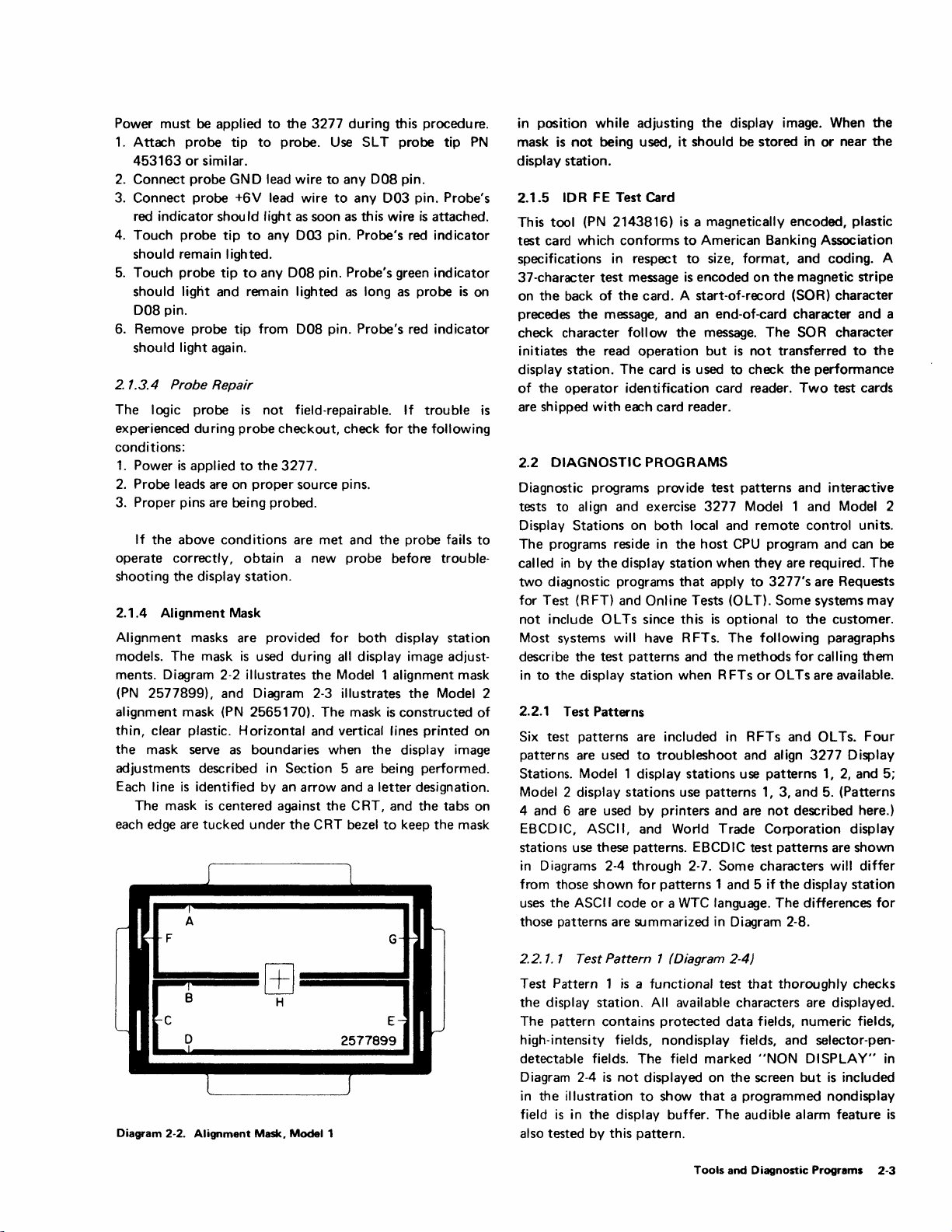
lOR FE Test Card
2.1.5
tool
(PN
This
test
card which
specifications
37-character
the
back of
on
precedes
check character
initiates
display station.
of
the
operator
are shipped with each card reader.
is
2.2
DIAGNOSTIC PROGRAMS
Diagnostic programs provide
tests to
Display
to
The programs reside
called
in
two
diagnostic programs
for Test (RFT) and
not
include OL Ts since this
Most
systems will have RFTs.
describe
in
to
the
2.2.1 Test Patterns
of
Six test patterns are included
patterns are used
Stations. Model 1 display
Model 2
4 and 6 are used by printers and are
EBCDIC, ASCII, and World Trade Corporation display
stations use these patterns. EBCDIC test
in
Diagrams 2-4 through 2-7. Some characters will differ
from those shown for
uses the ASCII code or a
those patterns are summarized
2143816)
conforms
in
respect
test
message
the
card. A start-of-record (SOR) character
the
message, and an end-of-card character
follow
the
read operation
The
card
identification card reader.
al
ign
and exercise
Stations
by
the
display station when R FTs
display
on both local and
the
display station when
Online Tests (OLT).
test
patterns and
to
stations
the
display image. When
stored
is
a magnetically encoded, plastic
to
American Banking Association
to
size, format,
is
encoded
the
message.
but
is
used
to
test
3277
in
the
host
CPU
that
apply
is
optional
The
the
in
troubleshoot
stations
use patterns 1, 3,
patterns
1 and 5 if
WTC
language. The differences
in
Diagram 2-8.
is
not
check
patterns and interactive
Model 1
to
methods
RFTs and OL Ts.
and align
use
and
on
the
magnetic stripe
The
SOR character
transferred
the
Two
remote
program and can
they
are required.
3277's
Some
to
following paragraphs
for
or
OL
Ts
patterns
and
not
described here.)
patterns
the
the
in
or
near
the
coding. A
and
a
to
the
performanct~
test cards
and
Model 2
control units.
be
The
are Requests
systems
the
calling them
are
3277
display
may
customer.
available.
Four
Display
1,
2,
and 5;
5. (patterns
are shown
station
for
~===
Diagram 2-2.
Alignment
[±]
=====
H
Mask. Model 1
2.2.1. 1
Test Pattern 1
the
The pattern contains
high-intensity
detectable fields.
Diagram 2-4
in
field
also tested by this pattern.
Test Pattern 1 (Diagram 2-4)
is
a functional test
display station.
is
the
illustration
is
in
the
All
protected
fields, nondisplay fields, and selector-pen-
The
not
displayed on
to
show
display buffer.
field marked "NON DISPLAY"
that
thoroughly checks
available characters are displayed.
data
fields, numeric fields,
in
the
screen
but
is
included
that
a programmed nondisplay
The
audible alarm feature
Tools
and
Diagnostic
Programs
2-3
is
Page 12
t'
r-
0
'-
E
'-
Diagram 2-3.
B
J
F
Alignment
11
-1.
-
Mask, Model 2
N
9
M
-
-
480
1920
CHAR
CHAR
H
.........
K
L
G
2565170
-----.
--
./
Paragraph 5.1.1 describes
procedure
during
2.2.1.2 Test Pattern 2 (Diagram 2-5)
Test Pattern 2
described in paragraph 5.2.1.
displayed in normal intensity. The audible alarm (if
installed) sounds when this pattern appears on
22.1.3
Test Pattern 3
described in paragraph 5.2.1.
displayed in normal intensity. The audible alarm (if
installed) sounds when this pattern appears on
22.1.4
Test Pattern 5 loads
available uppercase and lowercase character codes. The
that
uses Test Pattern
the
execution of several Troubleshooting Diagrams.
is
used
to
Test Pattern 3 (Diagram 2-6)
is
used
Test Pattern 5 (Diagram 2-7)
the
the
comprehensive checkout
1.
This
pattern
align
the
Modell
All
data
to
align the Model 2 image
All
data
display station buffer with
is
also used
display image
is
protected and
the
is
protected and
the
as
screen.
as
screen.
all
audible alarm (if installed) sounds when this pattern
on
the
appears
2.2.2 Requesting RFT Patterns
RFT patterns can be requested for
attached
control unit (3271). Patterns can be requested from
display station
patterns,
BTAM
Access Method)
Basic Telecommunications Access Method), and
cation program must
system programmer can verify
request RFT patterns are met. The eight test patterns (four
EBCDIC and four ASCII)
and their identification numbers are listed
screen.
3277
Display Stations
to
a local control
to
be displayed
the
controlling
(Operating System Basic Telecommunications
or
DOS
be
unit
(3272)
on
another.
CPU
must be operating under
BTAM
set
(Disc Operating System
up
to
accept test requests.
that
the
that
can be requested by RFTs
or
to a remote
To
display
the
appli-
requirements
in
Diagram 2-9.
one
as
The
to
2-4
Page 13

ABCDEFGHIJKLMNOPQRSTUVWXYZ
NON
DISPLAY
COpy
I Q # $ % ¢ &
COpy
?SEL
(Model 1 Patternl
ABOVE
~:
ABOVE
PEN
IN
( ) _ + ! ; f t < >? - =
IN
TEST
THIS LINE INSERT
I;
I /
01
2 3 4 5 6 7 8 9 ~ • - A
THIS LINE
> SEL
PEN
TEST
ADR-6G48
CK
(Model 2 Pattern)
Notes:
Diagram 2-4. Test Pattern 1
1.
AOR
NON
Use
- ctppears
OISPLA
Olawam
2.
3.
Y
2-8
only
Ie;
to
(USA
when
not
displayed
determlnP
EBCDIC)
patter')
unique
Ie;
called
chilrilctp.r
"'
Irr"n
()L
fEP
rr>p!.I(.;elr.~nts
wiWIl
A~";CII
vr
lllTe
1.1!)(ludges
.lrE'
u~ed
ToOls and Diagnostic Programs 2·5
Page 14

EEEEEEEEEEEEEEEEEEEEEEEEEEEEEEEEEEEEEEEE
H H
H H
H H
H H
,H
H
H
H
TEST
H *
0
00
DO
PATTERN
FOR
ALIGNMENT
UNPROTECTED
3275-1/3277-1
AREA
* H
H 0 ADR-6040 H
EEEEEEEEEEEEEEEEEEEEEEEEEEEEEEEEEEEEEEEE
appears
only
when
pattern
IS
called
In
from
OL
Note'
AOR
TEP
c
H
H
H
H
Diagram
2·5.
Test Pattern 2
Not£!
Diagram
2·6
AOR
2·6.
dpf..H.'ars
(HliV
Test Pattern 3
when
pattern
IS c<Jlled
111
from
OL
TEP
Page 15

ABCD~FGHI~«+I&JKLMNOPQR!);~
STU
V W x Y Z
~u
_ > ? :
~
~
, = ' , . $ * - / , G 1 2 34 5 6 7 8 9
ABCDEFGHIJKLMNOPQRSTUVWXYZG123456789
ABCDEFGHIJKLMNOPQRSTUVWXYZ8123456789
(Model
&-/
<;:.«+1
<;:.«+1
I"J/L
EOfVl
1
Pattern)
&-/
!$*);-,
!$*)j-'
,%
,~t=>?:#Qt="
CHECK55555
CHECK99
>?:n0'="
Note:
Diagram
I
Jse
27.
DlagrnJn
fest
28
to
deterrninf'
Pattern 5 (USA
unique
EBCDIC)
Lhdrdcter
repldU'n1t'nts
,,,,,'twn
A:,\::
I
l'
\",
T
~
1,!fHjlJd<WS
drt'
lJSPU,
Tools
dnd
Diagnostic
Programs
2-7
Page 16
Hex Code/Graphic
Language 4A 5A 5B 78
-USA
EBCDIC
USA ASCII-A
USA ASCII-B
Austrian/German
Danish/Norwegian
Finnish/Swedish
Portuguese
Spanish
United Kingdom
t
[
r
0 U U
{lS
0
A
~
$
! $
)
)
l
1
C
!
!
$
$
1
1
~
p+
t.
#
#
#
A
4-
A
cr
N
#
7C
@
@
fit
ii
0
0
A
-
•
@
7F
"
..
"
A
4-
A
0'
N
"
4F
I
I
I
I
I
I
I
t
I
SF
-.,
--,
~
-.,
--,
-.,
.....,
-.,
-.,
-Belgian,
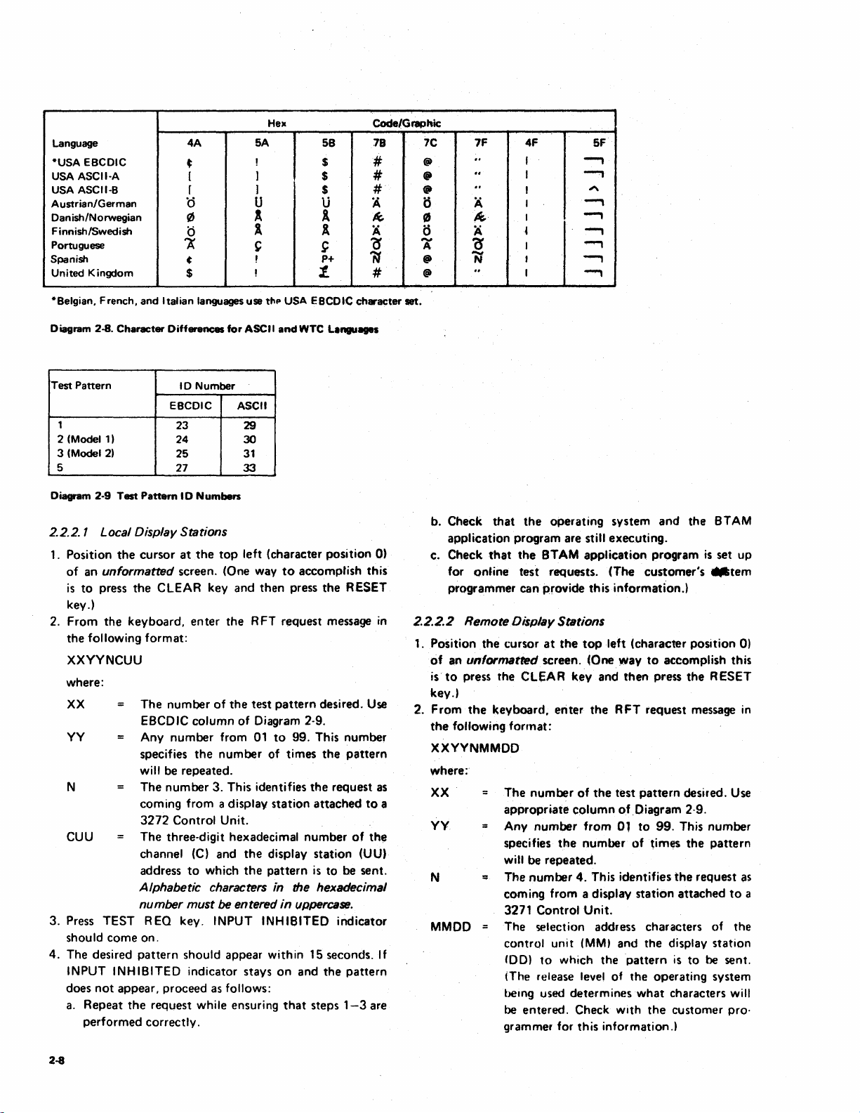
Diagram 2-8.
Test
1
2 (Model
3 (MocIe121
5
Diagram 2-9
2.2.2. 1 Local Display Stations
1. Position
2.
3. Press
4.
French,
and
Italian languages
Character
Pattern
1)
Test
the
of
an
unformatted
is
to
press
key.)
From
the
the
following
XXYYNCUU
where:
XX
YY
N
CUU
TEST
should
come
The
desired
INPUT INHIBITED
does
not
appear,
a.
Repeat
performed
Differences
EBCDIC
Pattern
cursor
the
CLEAR
keyboard,
format:
The
number
EBCDIC
Any
number
specifies
will be
The
number
com
ing
3272
The
three-digit hexadecimal
channel (C)
address
A/phabetic characters in the hexadecimal
number must
R EQ key. INPUT INHIBITED
on.
pattern
proceed
the
request
correctly.
10
Number
23
24
25
27
10
Numbers
at
the
top
screen. (One way
key
enter
of
column
from
the
number
repeated.
3. This identifies
from
a display
Control
Unit.
and
to
which
be entered
should
indicator
as follows:
while ensuring
use
for
ASCII
ASCII
29
30
31
33
left
and
the
RFT
the
test
of
Diagram 2-9.
01
the
the
appear
stays
t"p
USA
and
WTC L.nguages
(character
to
accomplish
then
press
request
pattern
to
99. This
of
times
station
display
pattern
in
uppercase.
within
on
and
that
eecotC
position
the
RESET
message
desired. Use
number
the
pattern
the
request
attached
number
15 seconds.
station
is
to
indicator
the
steps
of
be
pattern
1-3
character
0)
this
in
as
to
a
the
(UU)
sent.
If
are
set.
b.
Check
application
c.
Check
for
programmer
2.2.2.2 Remote Display Stations
1. Position
of
an
is
to
key.)
2.
From
the
that
that
online
the
cursor
unformatted
press
the
the
keyboard,
following
the
program
the
STAM
test
can
CLEAR
format:
operating
are still
requests.
provide
at
the
screen. (One
key
enter
XXYYNMMDD
where:
XX
YY
N
MMOD
The
number
appropriate
Any
number
specifies
witt be
:;
The
coming
3271
The
control
tOO)
(The release level of
bemg used
be
grammer
the
repeated.
number
from
Control
selection address
unit
to
which
entered.
for
of
column
4. This
determines
Check
this
system
executing.
application
(The
this
information.)
top
left
(character
way
and
then
the
RFT
the
test
of
.Diagram 2·9.
from
Ol
number
a display
Unit.
(MM)
of
identifies
and
the
pattern
the
with
information.!
and
the
program
customer's
to
accomplish this
press
the
request
pattern
to
station
what
desired. Use
99. This
times
the
the
attached
characters
the
display
is
to
operating
characters
the
customer
BTAM
is
set
_tern
position
RESET
message
number
pattern
request
of
station
be sent.
system
up
0)
in
~s
to
the
will
pro·
a
2-8
Page 17

3.
Press TEST REQ key. INPUT INHIBITED indicator
should
come
on.
4.
The
desired
iNPUT INHIBITED indicator slays
does
not
a. Repeat
pattern
shoUld appear within
appear, proceed
the
request while ensuring
as
follows:
on
that
15
and
steps
seconds. If
the
1-3
performed correctiy.
b. Check
application program are
c. Check
for
that
the
operating system and
stili executing.
that
the
BTAM application program
online test reQuests. (The
the
is
customer's
programmer can provide this information.)
pattern
are
BTAM
set up
system
2.2.3 Online Tests (OL
Online tests may
aid
in
maintaining 3277 Display Stations. Detailed descrip-
tions and instructions
diagnostic program binder
unit. Control unit
Most
OL T routines apply
three routines
apply
1. KEY - This routine handles
rupts from
the
function keyboard. The
presented on
CE
of
the
success
Th
is
routine also reads back
keyboard
2.
MAG
to
check lowercase character codes.
- This routine tests
Ts)
be
available,
for
ML
TGs also
to
display stations:
at
the
customer's
using OL Ts are
that
is
shipped with each
contain
to
control units. The following
contained
this information.
manually generated inter-
keyboard, selector light-pen, and program
results
the
display station screen, informing
or
failure
the
of
of
the
data
operator
the
interrupt
entered
identification card
reader and identification cards.
3. PAT - This routine
paragraph 2.2.1.
the
CRT after
message containing instructions
pattern
sequence precedes Test
displays
The
they
are initially called in. An explanatory
'test
the
test patterns described
patterns
appear in sequence on
for
running
Pattern
1.
option,
in
to
the
control
interrupts are
the
operation.
from
the
in
the
test
Tools
and
Diagnostic
Programs
2-9
Page 18

3.1
SYMPTOM INDEX USAGE
The
Symptom
encountered on
trations
images are
Index and illustrations as
method
Index lists
3277
that
show
also
contained
of
resolving display station problems.
trouble
Display
both
in
symptoms
Stations
correct and incorrect display
this section.
the
first step
that
could be
and features. Illus-
Use
the
Symptom
in
a systematic
The
index
divided into six major categories:
1. Display malfunctions.
2. Keyboard malfunctions.
Selector light-pen malfunctions.
3.
4. Power malfunctions.
CPU error indications.
5.
6. Operator identification card reader malfunctions.
Some categories are divided into subcategories, making it
easier
to
relate
the
trouble
in
the
index. Beginning
closely describes the display station trouble should
experienced
with
1A
1,
the
to
first
the
item
correct
that
be
item
most
used.
Categories and specific items are identified by a one-, two-,
or three-letter/number code (e.g., 1 A 1, 2G, or
of
the
column
into
the
Troubleshooting Diagrams
The right column of the
to take
index. The code specifies the
Symptom
to
remedy
the
display station problem.
in
Section 4.
I ndex specifies action
column directs the Customer Engineer
shooting diagram sheet
change. When more than
or
specifies a logic card (or cards)
one
card
is
4)
in
the
entry
to
a section trouble-
listed, isolate the
left
point
That
failing card by card swapping from among those specified.
the
others
to
Change the failing card and return
stock. The
right column may also specify an adjustment procedure
Section 5.
Diagrams 3-1 through 3-24 show both
incorrect display images.
illustrations
As an aid
to
aid in identifying display station symptoms.
to
rapid repair, diagrams
display images also specify
The
symptom
the
repair action.
correct
I ist refers
that
show incorrect
and some
to
these
Section 3. SYmptom Index
3.2 DEVELOPING SYMPTOMS
Display station malfunctions should be isolated offline
unless
the
trouble
through
type
the
control
are listed in Category 5 (CPU Error Indications).
Display station operations
is
for failure
1.
Selector light-pen operations.
symptoms
2. Display intensity
display).
3. Protected and numeric field operations.
4. Tab operations.
5. Erase input and erase field operations.
Test Pattern 1 contains fields
test
The
or
pattern may be loaded from
OL T.
Symptoms
marked with an asterisk
Offline
the
symptoms
following
removed.
1. Turn power on. (Always begin from a power-on reset
condition.)
2. Test cursor move keys
3. Test CLEAR key.
4. Enter four
to
5. Press Tab
6. Press Backspace
7.
Enter
four
8. Press Backspace
Enter
INS
four
in
9. Press
10.
11. Test DEL key.
Stop
the
when
the
first failure occurs.
occurs only when operating online
unit
to
the
host CPU. Failures
that
require a formatted buffer
to
become evident are:
control
that
(*)
(high intensity and non-
that
test
these operations.
the
system as an RFT
require a
in
the
formatted
Symptom
should be developed by performing
tl..'5t
sequence after
or
five characters.
(~)
key.
(+-) four times.
--+,
t,
..t.,
+-, ~ ,
the
I/O signal cable
~,
characters.
(+-) four times.
MODE.
or
five characters.
test sequence and go to
the
Symptom
Index.
+-'
of
buffer are
•
Index
this
is
Symptom
Index
3-1
Page 19

SYMPTOM
INDEX
Symptom
Note: Bad
failures ranging
checker
1.
DISPLAY
A.
B.
or
mIssing green
from
PN
9900453.
MALFUNCTIONS
No
Display:
1.
No
visible
characters,
Glow
2.
Intensity and Focus:
One
1.
2.
3. Block displayed
horizontal
Modell
Model 2 ten
scan
a.
INPUT
INPUT
b.
I 4. Display
effect
5. Characters
*6. Dual-intensity problems
7.
Display erratic (e.g., display flashes, characters move, more than one cursor)
I
8. Screen
9. Retrace unblanked
10. Random data on screen. INPUT
11. Cursor on
One
12.
dot
wire
grounds on display stations
intermittent
light
or
indicators displayed.)
only
on CRT (Diag 3-9)
line on
- Full raster on screen (Diag 3-11)
24
rows
lines) (Diag 3-12)
INHIBITED
INHIBITED
too
dim
usi
ng
display focus
out
of
full
of
lines
left
side
at character location zero cursor
to
catastrophic.
or
glow on CRT. (Device Check
CRT
(Diag 3-10)
of
nine
scan
lines
..................
in
every character
lighted
not
or
too
bright (No
control).
focus (Diag 3-18)
or
characters displayed
.............
.............
in all rows . . . . . . . . .
position;
................
lighted
control
INHIBITED
or
Verify
proper grounding
not
................
OR
with
space
between
cursor normal (Diag 3-14).
..............
of
intensity),
that
should
.
.
lighted
position
control
indicated;
each
or
dim
not
units can
by
row
and blurred (no
cause
using ground
no
cursor,
(one
row
.
.
.
Diagram Sheet
Direct
Action
Sheet 2
Sheet 4
Sheet 4
.
of
Sheet 5
Change card J2.
Change card
Sheet 5
Sheet 5
Sheet 6
Sheet 6
Sheet 6
Change cards H2, J2, K2.
Change card H
Change card H2.
Change card J2.
K2.
or
Repair
2.
C.
Display Position and Size:
Horizontal
1.
Vertical size
2.
Both
No
space
3.
•
Requ
ires a
formatted
3-2
size
too
horizontal
between rows
buffer.
too
large
or
too
large
or
too
and vertical size
of
characters (Model 2
small (vertical normal) OR
small (horizontal normal, Diag 3-8)
too
large
or
too
small
only)
(Diag 3-16) . . . . .
..
Adjust
analog card.
of
range
of
change analog card and
card J2.
If
less
than
direction, adjust analog
If
card.
if
change
supply.
Sheet 7
more than
display size erratic,
HV
If
adjustment,
1"
in either
1",
power
out
or
Page 20

Symptom
1.
DISPLAY MALFUNCTIONS (Cont)
C.
Display Position and Size: (Cont)
4. Rows
5. Display
of
characters
not
centered (Diag 3-7)
not
6. Display tilted (Diag 3-6) . . .
D.
Dlaracters:
1. No characters displayed,
problem only.) . . . . . . . . . . . . . . . . . . . . . . . . . .
0 isplay
2.
than one cursor
3. Character(s)
4.
Screen full
a. Quote mark
out
of sync. (Characters may be recognizable
is
seen. INPUT INHIBITED
not
formed correctly wherever displayed
of
quote
in
location 0 and cursor in location 1 after
5. Wrong character displayed from program, keyboard,
a. Without Device Check
b. With Device Check . . . . . . . . . . . . . . . . .
6.
Data displayed
Screen full
7.
8.
Screen slowly fills with character
INHIBITED
that
should
of
one character with
not
lighted
9. Attribute characters displayed
SYMPTOM
INDEX
(Cont)
Diagram Sheet or
Direct Action Repair
evenly spaced
Change analog card
See centering procedure
(5.2.1.5).
See
yoke
adjustment
procedure (5.2.1.4)
but
cursor displayed. (See Symptom 2B4 if keyboard
..
Sheet 7
but
are moving, and more
not
lighted.) (Diag 3-15) Sheet 6
on
screen Change card K2.
marks (no Device Check) . . . . . . . . Change cards A2, K2.
POR
Replug connector inside
keyboard.
or
POR:
Change card K2.
Sheet 7
not
............
or
without
of
INPUT INHIBITED lighted
last keyboard key pressed. INPUT
.
Sheet 8
Sheet 8
Change card A2.
Sheet 8
E.
Cursor:
1.
No cursor on screen,
No
cursor with INPUT INHIBITED lighted. Cursor cannot
2.
by
Power
Cursor appears normally. INPUT INHIBITED lighted
3.
4. Cursor under
INHIBITED
5.
Cursor under all character positions,
6. Cursor
7.
Cursor
No
8.
cursor, and INPUT INHIBITED
character enters until
character.
9.
Screen slowly fills with cursors . . . . . . . . . . . . . . . . . . . . .
10. Cursor appears
PORe
may blink
No
11.
cursor on screen after
each row displays
but
rest
of
On
Reset
or
CLEAR key
display normal (no Device Check)
be
..................
.....
returned
...........
all
or
most character positions, and Device Check indicated (INPUT
lighted) (Diag 3-13)
not
positioned correctly under a character; may be in character area
too
long
or
too
short
80
characters
...................
but
Device Check
not
indicated (Diag 3-13) .
. . . . . . . . . . . . . . . . . . . .
not
on. Partial cursor appears as each
in
row appear with partial cursor under each
Occurs on one row at a time . . . . . . . . . . . . . . . . . .
in
Characters
three or four rows equally spaced
mayor
may
not
enter and appear at cursor location. Display
on
left side
of
display after
.............................
PORe
Characters may enter,
as
character enters. (INPUT INHIBITED
but
only first scan
not
lighted)
to
screen
1ine
of
.
Change card
.
Sheet 9
.
Sheet 9
.
Sheet
K2.
10
Change card K2.
Change card
Change card
K2.
K2.
Change card J2.
Change cards A2, C2, H2.
.
Sheet 10
Change
card
Symtom
J2.
Index
3-3
Page 21
SYNIPTOM
INDEX
(Cont)
Symptom
1.
DISPLAY MALFUNCTIONS (Cont)
F. Indicators:
1.
No indicators light. (Characters and cursor normal.)
*2. One indicator fails to light . . . . .
One indicator lit when it should
*3.
2.
KEYBOARD MALFUNCTIONS
Note:
If
card reader feature
at
feature logic card
If
keyboard operates correctly with card removed and cable swapped, change card N2,
location N2, and move keyboard cable from socket Z4
and return keyboard cable
cable swapped, select symptom
A.
All
Keys
is
installed on failing display station, remove card reader
to
socket Z4.
that
not
be
.....
If
keyboard still fails with card removed and
best describes failure.
.
to
1. Keyboard inoperative . . . . . . . . . . . . . . . . . . . . . . .
2. Keyboard operation erratic (INPUT
3. Diagonal row of
INPUT INHIBITED not lighted
enter.
dots
appears starting
INHIBITED
at
..
on
after certain keys.) Sheet 12
lower left corner of screen as characters
. . . . . . . . . . . . . .
socket Z1.
..
..
Diagram Sheet
or
Direct Action Repair
11
Sheet
Sheet
11
Sheet 9
Sheet 12
Change card J2.
B.
Character Keys:
one
1. Wrong character for
key
2. Wrong character for more than one key
No
characters
3.
*3a. Correct character enters,
No
character enters for all keys; cursor advances with each key depression. Dots
4.
may appear
Alpha characters enter into "numeric
*5.
numeric lock feature
on
enter
for all keys .
but
one
line. (INPUT INHIBITED indicator does
is
installed. See
*6. Numeric characters cannot enter
7. Typamatic failures
...............
8. Cursor disappears when character enters
Cl)aracters entered
9.
INHIBITED
not
not
lighted.)
displayed. Cursor move keys work correctly. (INPUT
..
..............
INPUT INHIBITED lights for one or more keys
not
light.)
only"
Diag
in
"numeric
fields. (Verify
6-10.) . . . .
only"
fields
that
keyboard
.
....
. . . . . . . . .
...................
keyboard
See
check
procedure 5.1.4.
Sheet 12
.
Sheet 13
Sheet 7
Sheet 13
Sheet 13
Change card
See
B2.
keyboard
check
procedure 5.1.4.
Sheet 14
Change cards A2,
B2.
G2.
• Requires a
formatted
buffer.
Page 22

SYMPTOM INDEX (Cont)
Symptom
2. KEYBOARD MALFUNCTIONS (Cont)
C.
Cursor Control Key Failures:
1.
Failure
of
any
or
all cursor move keys:
2. Data moves
to
left when +-key pressed . . . . . . . .
D. Operator Function Key Failures:
*1.
ERASE FIELD
*2. ERASE INPUT
INS
3.
3a.
MODE
INPUT INHIBITED lights when
.....
......
.
.
4. DEL
5.
RESET
......
.
E. Program Access Key Failures:
1.
CLEAR
2. ENTER,
......
PAl,
PA2, PA3, TEST REO,
.
F. Keyboard Assembly
1.
Keyboard Mechanical Failures (includes audible feedback) .
2. Keyboard
Electrical Failures . . . . . . . . . . . . .
~
J.
c~rsor
moves from last
or
PFl-12
t......
-+t
+-
IE-
to
first character position
Diagram
Sheet
or
Direct Action Repair
Sheet
14
Change cards C2, H2.
Sheet
18
Sheet
18
Sheet
18
Change card
Sheet
Sheet
Sheet
Sheet
Sheet
J2.
19
19
20
20
20
Sheet 21
G. Audible Alarm Failures:
1.
Fails
to
sound
2. Sounds when it should
3.
SELECTOR LIGHT-PEN MALFUNCTIONS
A. Nothing happens when tip switch closed
*
*B. Lines appear and remain through
not
all detectable characters with
detect
*C. Lines always appear through all detectable characters, even when pen
*0.
Data
not
entered when selector light-pen initiates
1.
INPUT INHIBITED
INPUT INHIBITED lights
2.
does
not
light
..............
entry
into system:
.
*E. Selector light-pen action changes verification characters correctly,
INHIBITED lights
*
Requires a formatted
buffer.
...........................
attempted
not
used
but
INPUT
Sheet 21
Change cards G2, H2.
Sheet
22
Sheet
22
Sheet
22
Change card
Change cards G2,
Change card
.
M2.
M2.
02.
Symptom
Index
3-6
Page 23

SYMPTOM INDEX
(Cond
Symptom
4. POWER
5.
CPU
Note: (Device
condition.
A.
B.
C.
D.
E.
MALFUNCTION
ERROR
Device
Operator
Display
Control
characters
Error
1.
2.
INDICATIONS
)
not
cannot
station
unit
may
Printouts
Device
Device
available
Checks
Checks
*3. Device Checks (parity)
4.
Transmit
check
always
cannot
appear
Checks
is
indicated
use
attention-generating
appears
write
after
(no cursor)
(too
CLEAR
many
busy
to,
cursors)
by
INPUT INHIBITED light
keys
and/or
selector
to
or
control
read
key
unit
from,
display
operation.)
on
due
light-pen successfully
station
correctly.
to
an
(Random
error
Diagram
Direct
Action
Sheet
23
Sheet
26
Sheet
26
Sheet
26
Change
Sheet
9
Sheet
10
Sheet
7
Sheet
27
Sheet
cards
or
Repair
G2, H2,
J2.
F. Read Modified (MDT
1.
Selector
2.
Selector
3.
Keyboard
G.
Programmed
H.
Keyboard
I. Program erase
6.
OPERATOR
A. Cards
B.
Incorrect
c.
Cursor
*
Requires a formatted
pen
pen
audible
remains
IDENTIFICATION
do
not
feed
number
does
not
changes
fails
fails
to
disabled
of
unprotected
through
of
characters
move
buffer
bit)
to
set
set
alarm
as
card
Failure:
designator
MDT,
MDT .
failure
after
program
data
CARD
reader
read
feeds
character
and
unsuccessful; erase
READER
through
correctly,
INPUT INHIBITED
attempt
to
MALFUNCTIONS
reader
but
enable
from
INPUT INHIBITED lights Change
does
not
light Change
Change
Sheet
it
keyboard
successful
Change
Change
Sheet
Sheet
Sheet
card
card
cards
21
card
card
27
27
28
02.
M2.
A2,
G2.
G2.
C2.
3-6
Page 24

See Diagram
2-4
for
greater detail
of
the
test
pattern
data.
See Diagram
2-4
for
greater
detail
of
the
test
pattern
data.
Diagram
See Diagram
Diagram
3-1.
3-3.
Test
Pattern
2-5
for
Test
Pattern
Model 1
(Adjust
1,
Model 1
greater detail
2
malfunction
yoke,
5.2.1.4.)
of
the
test
produces
pattern
data.
similar results.
Diagram
See Diagram
Diagram
3-2.
3-4.
Test
Pattern
2-6
for greater detail
Test
Pattern
Model 1
(Adjust
yoke,
1, Model 2
3
malfunction
5.2.1.4.)
of
the
test
produces
pattern
data.
similar results.
Diagram
3-5.
Yoke
Back
Too
Far
on
CRT
Neck
Diagram
3-6.
Yoke
Tilted
Symptom Index 3-7
Page 25

Model 1 malfunction
(Adjust
centering rings, 5.2.1.5.)
produces
similar
results.
Model 1 malfunction
(Adjust
analog card.
Mod€1
2,5.2.1.7.)
produces
Model
similar
1,
5.2.1.6,
results.
Diagram
Diagram
3-7.
3-9.
Centering
(Troubleshoot
Glow
Only
Rings
Not
on
CRT
(Troubleshoot
Adjusted
on
Diag 4-1, Sh
on
Diag 4-1, Sh 5,
Properly
4,
1
A2.)
182.)
Diagram
Diagram
3-8.
3-10.
Character
(Troubleshoot
Single
Horizontal
(Troubleshoot
Height
Too
line
Small
on
Diag4-1,Sh
on
CRT
on
Diag 4-1, Sh
4,
181.)
5,182,)
Diagram
3-8
3-11.
Model 1 Raster
Diagram
3-12.
Model 2
Raster
Page 26

Model 1
malfunction
(Troubleshoot
INPUT
INHIBITED
K2')
card
produces similar results.
on
Diag 4-1, Sh
is
on.
Ifioft
10,
1E4
change
if
Model 1
(Change card
Change
malfunction
J2
if
card
K2
if
produces similar results.
INPUT
INHIBITED
off.)
is on.
Diagram
Diagram
3-13.
Cursor in Every
Model 1
The
number
.[Troubleshoot
3-15.
No
malfunction
density
of
each
of
characters
on
Horizontal
Model 1 display is
Sync
Row
produces similar results.
row
is determined
in
that
4-1,
row.
Sh
same
6102.)
except
Diag
by
for
the
size.
Diagram
Diagram
3-14.
Box in Every
This
failure applies
(Troubleshoot
3-16.
No
Interrow
Model 2
(Troubleshoot on Diag 4-1,
malfunction
Character
Position
to
Model 2 displays
on
Diag 4-1, Sh 7, 1 C3.)
Spacing
produces similar results.
Sh
only.
5, 1 B5.)
Diagram 3-17.
Correct
Display
after
POR
Diagram
3-18.
Out
of
Focus
I "lage
Symptom
Index
3-9
Page 27
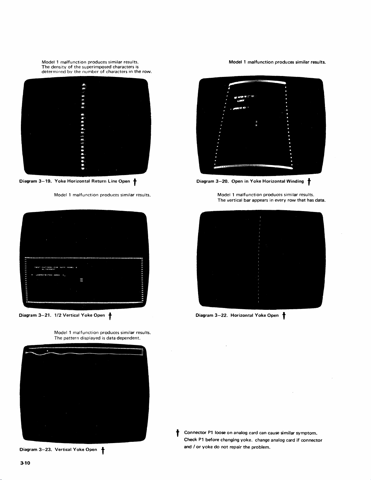
Model 1 malfunction
The
density
of
determined
bv
the
the
produces
superimposed
number
of
characters
similar
characters
results.
in
the
is
row.
Model 1 malfunction
produces
similar
results.
Diagram
Diagram
3-19.
Yoke
Model 1 malfunction
3-21.
1/2
Model 1 malfunction
The
Horizontal
Vertical
pattern
Return
Yoke
Open
displayed
Line
produces
t
produces
is
data
Open
t
similar
results.
similar
dependent.
results.
Diagram
Diagram
3-20.
Open
in
Yoke
Model 1 malfunction
The
vertical
bar
3-22.
Horizontal
Horizontal
produces
appears
Yoke
in
every
Open
Winding
similar
row
t
results.
that
t
has
data.
Diagram
3-10
3-23.
Vertical
Yoke
Open
t
t
Connector
Check
and /
or
P1
yoke
P1
before
do
loose
changing
not
on
analog card can cause
yoke.
change
repair
the
problem.
similar
analog
card
symptom.
if
connector
Page 28

Section 4. Troubleshooting Diagrams
I The Troubleshooting Diagrams (29 sheets)
be
used
as
should
3). The diagrams are flowcharts arranged in a sequence
ensures successful trouble resolution
The steps
because successive steps depend on
obtained
seem
discouraged to avoid unnecessary duplication
prolonged service
Sheet
caused by a display station problem or by a control
problem. Subsequent flowcharts cover display, keyboard,
selector pen, and card reader malfunctions. Additional
sheets analyze power troubles and miscellaneous keyboard
assembly
Observe good safety habits
station with power on.
anode,
voltage distribution points. Always remove power from the
display station when removing
avoids damaging circuitry
feeding it.
The flowcharts use
"change card XX". "Replace" means to reinstall the same
card
new card from stock. The
probable cause of the failure.
Two unique symbols are used
symbol
means
in
the symbol. Seven logic probe conditions can be seen
with
from the probe symbol specifies one
ditions.
specified
flowchart.
specified
"Other".
the flowcharts and their definitions are
1.
Red
2.
Green - solid green.
Red
3.
blink.
in
in
illogical and shortcuts may seem apparent, deviation
1 determines whether
electrical and mechanical troubles.
the
that
was earl
to
probe (with
the
older style probe
If
in
result, use
The seven logic probe observations specified
- solid red.
Blink - solid green with one (and only one) red
directed by
the
flowcharts must be followed
preceding steps. Although
calls.
yoke assembly,
ier
removed; "change" means
the
the observed condition
the
flowchart, continue down
If
the observed result
the
the
Symptom I ndex (Section
the
the
symptom experienced
while working on
High
voltage
the
HV
power supply, and
or
replacing logic cards. This
on
that
the
terms "replace card XX" and
old card being changed
in
logic probe) the point designated
(PN
453652).
is
part
of
the flowchart labeled
in
this section
in
a minimum time.
in
sequence
actions and resu Its
the
sequence may
of
effort and
the
display
is
present at
card
the flowcharts. The
of
is
the
different from the
as
follows:
the
or
other
cards
to
install a
is
An
output
the seven con-
same
as
that
part
of
CRT
that
is
is
unit
the
the
line
that
the
in
4. Green Blink - solid red with one (and only one) green
blink.
5. Pulsing Red - solid green with
of
pulses
as
frequency
stay on.)
6. Pulsing Green -
of
frequency
stay on.)
7.
Red and Green - approximately equal red and green
pulses (any frequency).
The same conditions can be observed using the new G
(General Logic Probe),
older-style logic probe
red
to
indicate a plus
indicate a minus level. This difference must be kept
when troubleshooting with
in
this manual were designed for use with the
logic probe. ' ,
The card-shaped symbol
appearing
location
problem.
1. Turn power off.
2.
3. Turn power on.
4. Verify
5.
6. Return display station
the
specified. Change
stock.
problem, check
these card locations.
voltages and voltage pins.
removal procedures. Because
utility
Section 5. Flowchart references
as
Section 5 where
of
It
Change card (5).
that
Replace covers.
When
more than one card
failing card by card-swapping from among those
If
changing
The flowcharts
as
three-
or
pulses
at
the
end
the
card(s)
also means
trouble
the
all voltages
standalone procedures, they are contained
four-digit numbers, indicating
the
long as green indicator appears
solid red with regular green pulses. (Any
as
long as red indicator appears
PN
453212. The difference from
is
that
level
and
of
a diagnostic sequence gives
to
be replaced
to
take
is
repaired.
to
failing card, and return the others
the
specified cards does not repair the
Use
call
out
procedures are found.
regular red pulses. (Any
to
LP
the
the G LP
DOWN
the
GLP because the flowcharts
the
user.
is
listed
on
the
Diagram 6-14
certain check, adjustment, and
uses
UP
in
place of
in place
that
following action:
in
the
A 1 board backpanel
of
their length and their
to
these procedures appear
of
green
ol~r-style
will
repair
symbol, isolate
to
identify
the
paragraphs
in
to
mind
the
the
to
the
to
at
in
In
Troubleshooting
Diagrams 4-1
Page 29

Check
properly before beginning
Basic cards
Model 2 basic cards
I should also
shows logic board card plugging
that
all
basic
for
Model 1 display stations
are
be
installed and seated properly. Diagram 6-12
cards
are
installed
the
troubleshooting procedure.
C-K. Applicable feature cards
for
display stations
are
C-E
and
and
with
seated
G-K.
features (1/2 board); Diagram 6-13 shows card plugging
. display stations
The
logic probe
isolate failing cards. Ensure
correctly before troubleshooting.
paragraph 2.1.3.3
no
that
have features installed (2/3 board).
is
used
extensively in this section
that
the logic probe
Use
to
check
out
the probe.
for
to
is
operating
the procedure in
4-2
Page 30

I
Example
not requi
1.
CLEAR
to Null
2.
CUf'IOr
3.
Image
4.
Image
of _ openItionr
..
CU:
key
does
not
••
PCIIitl_lng keys.
quality.
.iz
•.
clear
that do
buffer
Display station
troubl.
SWop
coo>ciai
betw
..
n the
stations.
reportee!.
cabl.,
two
di'pl
No
Trouble
is
probably in
display
stotion.
If
verlfic:otlon
pnlYe
trouble
stotion,
described
Yes
No
Assume
displ
ay
Symptom Index and
Troubleshooting Diagrams
to
resolve problem.
ay
further
is
required
is
in
display
perform operotions
at
left.
that
trouble is in
station.
Use
to
Dia
..... m 4-1. Display Station Troubleshooting Diagrams (Sheet 1
of
Yes
No
No
29)
Originol
probably
ccable
connection
intermittent
that
cannot
at
this tim
failur.
was
a loose cooxial
Or
on
problem
be
resolved
•.
Troublelhooting DWgrams 4-3
Page 31

1A1
•
Pr
i mary power
plugged
• Power switch turned
on (Pull).
• Turn
to maximum (full
clockwise).
Bri
in.
ghtness
cord
contra
I
Yes
• Turn power
•
Open
e
Check
poor
A-AIZ3.
e Check for loose
connector
card.
(5.3.1).
connector
off
side
covers
for loose or
on
•
ot
anaiog
• T urn power
• Remove
•
• Turn Brightness control
• Press
• Turn Brightness control
off
feature
A2, 82, M2. N?
T urn power
on.
to minimum (fully
counterel
ockwise).
and
hold INTEN
CRT
switch.
toward maximum.
.
card(s).
•
•
Compare
Diags
Release
switch.
3-19
INTEN
No
display
to
3-23.
CRT
with
Yes
Sheet
Yes
• Turn
4
•
•
• Power on ond
Replace
A2,
82,
Change
(Mod
Mod
2,
(5.2:
power
feature
analog
I,
5.3.3.4).
I).
off.
M2,
N2.
5.3.3.3;
adjust
card(s)
cord
Sheet
3
• T urn power off •
Change
analog
1,
2,
5.3.3.4).
5.3.3.3;
and
adjust
card
Sheet
4
•
(Mod
Mod
• Power on
(5.2.1).
Diagram 4-1. Display Station Troubleshooting Diagrams (Sheet 2
of
29)
• Turn
pawer
•
Replace
feature
A2, 82, M2, N2.
•
Chonge
analog
(Mod
1,
5.3.3.3
Mod
2,
5.3.3.4).
• Power on
(5.2.
and
n.
off.
card(s)
card
adjust
Yes
•
Tu"'"
pawer
•
Change
yoke
• Adjust
(5.2.1).
• Replace
A2, 82, M2, N2.
•
U~
check
(5.1.2)
to
functions
off.
(5.3.3.2).
feature
procedure
verify
are
card(s)
all
normal.
Page 32

Sheet
~
e Chonge fUM.
e
Turn
power
on.
Yes
e Remove
CRT
cone
shield
e Connect
e Turn power
socket and
(5.3.3.2).
CRT
on.
socket.
No
Check cables from
board
to
C/TB I ond
PC
board
from
fefTO
to
~onsformer.
No
e
Repoirfoult.
e Check
out
unit
for
pc-oper
operotion.
Sheet
~
e
Turn
power
CRT
cone shield
CRT
off.
sock.t
(5.3.3.2).
ond
e
Remove
e Connect
socket.
No
Yes
PC
e
Turn
power
Yes
Chonge vol toge
distribution board
!Diog.
7-6\.
CRT
CRT
I,
5.3.2.6,
5.3.2.7;
2,5.3.2.8,
5.3.2.9).
oH.
socket.
'4.
e Remove
e Measure resistance
between
pins I ond
Chonge ferro transforMer
(Mod
Mod
e
Tum
power aH.
e Remove
e Measure r
between
piN
I ond 14.
Check cobl
CRT
,ocket
or broken
CRT
socket.
..
istance
CRT
..
ond
for
l_
connections.
e
Turn power
e Reploce
e Chonge onalog cord
Mod
e Power
(Mod
2,
(5.2.1).
off.
cone
shield.
I,
5.3.3.3;
5.3.3.~).
on
ond odJust
Diagram 4-1. Display
Station
Troubleshooting
Diagrams
(Sheet 3 of
29)
Troubleshooting Di8gqms 4-6
Page 33

• Tum
power
• Remove
cover.
• Remove
A2, 82, M2,
• Turn
power
off.
right
feature
on
side
N2.
.
cordis)
Sheet 2 Sheet 2
Meaoure
following
voltage
at
PS2)
,.~
return, (Oiag
HVPS
(011/
10
7-14).
Remove
push-on connec:tar
Ifroln
supply
pin 3 (IN)
1
___
de
voltage
connector on wi
• Change analog ecwd.
(Mod
I,
Mod
2,
•
Power
on
(5.2.1).
at
...
5.3.3.3
5.3.3.-4) .
and
odj
and
..
t
Yes
• Turn
po_r
feoture
82,
M2,
1,5.3.3.3
2,5.3.3
off.
N2.
.•
cordh)
)
• Reploce
A2,
• Change analog cord
(Mod
Mod
• Power on and odjus
(5.2.1).
Meaoure
following
voltages
with
YOM
15Y
scale.
negotive
return.
t
Measure
voltage
board terminol
(Oiog
7-11)
distribution
•
Verify
Reference
leod to
de
voltage
distribution
11.
boord .
repoir.
on
on
Me
......
e
voltage
orc-wppression
terminol E8. (Oiag
7-\5)
on
board
S
.....
3
~m
4-1. Dispbtv
Stftion
Troubleshooting
Diegrems
(ShMt
4 of
29)
Page 34

• Remove
•
Adjvst
Contro'
ILlpp',5
left
Focus
0""
2.:
H V
cover.
using
JX)wer
3,
rocus
• Turn
• Change
Mod
Mod
• Power
(5.2.1
power
off
analog
1,5.3.3.3
2,
5.3.3.4
on
and
).
.
cord
adjust
Check
while
control
mini
....
um.
voltoge
turning
from
maximum
(Oiog
at
BIAI
Brightne
7-12)
..
to
P3-2
(~.
• Turn
• TUln
brig
clockwise
contrast
•
mwcin'1um
maxirnufT'
CheCk
vo"oge
....,~ile
tur~in9
control
f
..
o,.... ",0)(1"...:,.
Q'
B.
ight"'lE!''!t5
Yes
Checlo
vol'age
at
'''pply pic
whl
..
0d,u.'ing
iometer
eo·
oft
H
'.
IX>weo
10
r
H\
I.
'juDP!
•
y
power
CheCk
~
OCuS
potent
Diog 7-14)
;,
....
f)O
......
•
C~onge
) 3 2
•
'.;~rj~y
C
k2B
......
to
fi.
Diagram 4-1. Display
Station
• Turn
power
off •
Change
control
•
(5.3.3.5).
•
Verify
repair.
Troublnhooting
•
Turn
power
•
Model
1 -
Change
suppression
•
Model
2 -
Change
distribution
•
Verily
repair.
• T urn
power
•
Change
(Moo
Mod
2,5.3.3.4)
• Power
(5.2.1).
Diagrams (Sheet 5
off.
board.
boord.
analog
I,
5.3.3.3.
On
of
ono
orc-
(Diog
VOltage
(Dioq
off
odivst
29)
.
cord
7-3).
7-61.
•
Turn
power
•
Change
5.3.3.61.
•
Verdy repair.
con'rol
off.
Troubfnhooting
Diagrams 4-7
Page 35

I
• Turn
power
•
Change
analog
(Mod
1.
5.3.3.3
"""d 2. 5. 3 . 3 .4 )
• Power
on
and
(5.2.
I,.
off.
card
adju,t
• Turn
power
Open
Change
,Mod
Mod
Power
'5.2.
off.
right
side
feature
power
off
analog
1.
5.3.3.3'
2, 5. 3 . 3 . 4 I
on
and
I,.
•
• Remove
(A2, 82, M2, N21.
• r",n
•
•
cover.
cordIs)
.
card
adjust
•
Turn
power
• Remove
• Remove
A2,
82, M2,
•
Turn
power
off.
right
feature
on.
side
N2.
cover.
card(s)
Sheet 8
Diagram 4·1. Display Station Troubleshooting Diagrams (Sheet 6 of
29)
Page 36
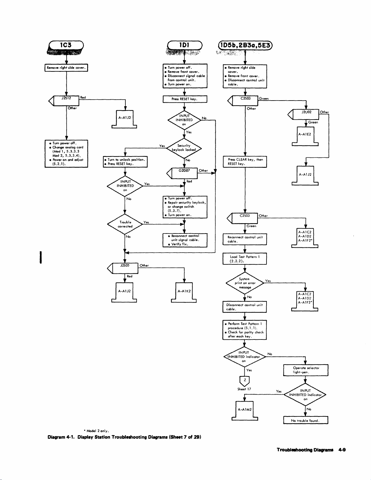
•
Tum
power off •
Remove
front
control
power
on.
unit.
cover.
•
• Disconnect signal cable
from
•
Turn
•
Remove
right side
cover.
•
Remove
front cover.
• Disconnect control unit
cable.
•
Tum
• Change anolog card
(Mood
Mod
• Power
(5.2.1).
I
power
1,
2,
5.3.3.4).
on
off.
5.3.3.3
and adj ust
Red
•
Tum
power
• Repair security keylock,
or change switch
(5.3.7).
off.
Green
Diagram
*
Moodel 2 only.
4·1.
Displav Station Troubleshooting Diagrams (Sheet 7 of
29)
• Perform Test Pattern 1
procedure
after
for
each
Sheet
(5.1.1).
parity check
key.
17
• Check
No
Yes
Troublelhooting Diagrams 4-9
Page 37

Sheet
Displ
include
cord
without
light-pen.
2,4,6,9,
ay
statio"
keyboard
reader
..
with
leclar
10,26
features
and
or
•
Move
from
•
Replace
feature
•
Tum
• Test
operations.
keyboard
Z4
Ia
keyboard
cards
power
keyboard
Zl.
on.
(A2,
cable
82).
Yes
•
Replace
feature
• Turn
• Test
operations.
keyboard
cards
power
keyboard
(A2,821.
on.
Yes
• T urI"
power
Replace
feature
Replace
feature
previolJsl y
Move
keyboard
ho'"
Zl to Z4.
off.
cord
card
light-pen
card
removed.
reader
(N21.
(M2)
coble
if
• Turn
power
off
light-pen
card
power
keyboard
off.
cord
cord
keyboard
to
Z4.
on.
reader
IN2l.
.
1M2,.
coble
• Replace
feature
•
Turn
• Test
operations.
• Turn
•
Replace
feature
•
Move
frolT'
power
Zl
-""od.1
•
•
•
2
onl
y.
Diagram 4-1. Display Station Troubleshooting Diagrams (Sheet 8
No
of
29)
4-10
Page 38
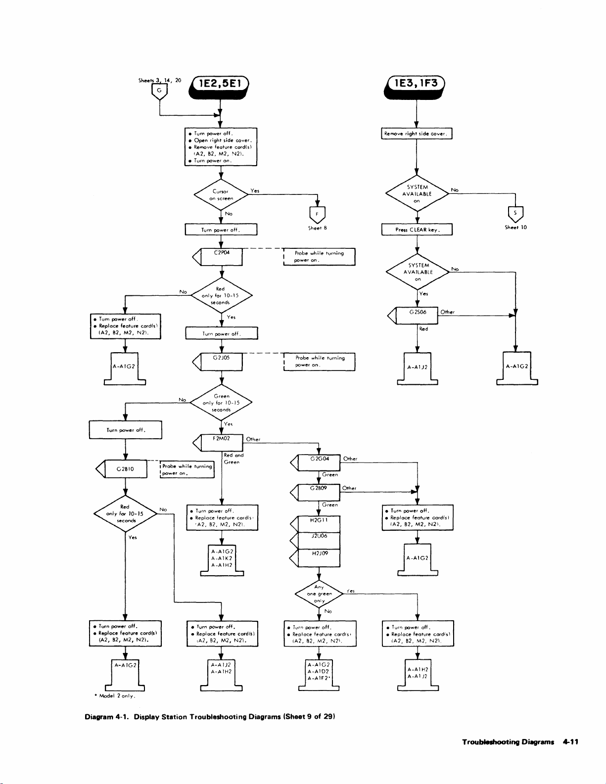
• Turn
•
Open
• Remove
IA2,
• Turn
power
right
82,
power
off.
side
feature
M2,
on.
cover.
card(s)
N21.
Probe
power
Probe
power
Sheet
while
on.
while
on.
8
turning
turning
Sheet
10
*
Model 2 only.
Diagram
I
Probe
while
on.
turning
I
power
Yes
4·1.
Display Station Troubleshooting Diagrams (Sheet 9 of
29)
Troubleshooting Diagrams 4-11
Page 39

Sheets
9,
28
•
Disconnect
from
• Remove
(A2,
• T
ur"
COr'ltrol
feature
82,
power
M2,
signal
unit.
on.
card(s)
N2I.
Yes
coble
Yes
• Turn power
•
•
• Remove
off.
Open
front
Disconnect
(A2, 82, M2, N2).
cover.
CU
feature
cable.
cord(s)
Green
Other
• Turn power
•
A2, 82, M2, N2.
• Turn power
Remove
off
feature
on.
•
cord(s)
Otfter
Other
Other
Green
Other
Model 2 Only
I
Diagram 4-1. Display Station Troubleshooting
4-12
Di.gr.ms
(Sheet
10
of
Other
Other
Other
29)
Page 40

• Turn POW"
• Remove
front
•
Disconnect
from control lJnil.
• Tu,n
po_'
off.
cove,.
lignal
on.
cabl.
•
Display
attached
station
10
an
mUlt
active
be
Diagram
4·1.
Displav
Station
Troubleshooting
Diagrams
(Sheet
11
of
291
•
Turn
po_r
• Repair
security
(5.
•
V.rl
off.
cabl.
Or
k.ylock
J.
7).
fi".
Troubleshooting
change
switch
Diagrams
4-13
Page 41

Probe
while
pressing a
and
RESET
alternately
character
key.
key
Remove
·
Disconnect
Press
·
·
Pre.s
·
RE5ET
Space
Probe
listed
right
CU
pin.
in
side
key.
bar.
cover.
cable.
2A2-2B2
Probe 1
B2505
B2S08
B2509
B2502
B2U05
B2Ml0
B2U09
B2Mll
B2513
Code
G
R
G
G
G
G
G
G
G G
Chart
G
R
Probe pins
PrObe
pi,,~
I
Diagram
No
Yes
4-1_
Display Station Troubleshooting Diagrar'ns (Sheet
12
of
P'ohif' pin,;
291
4-14
Page 42

• Press
CLEAR
and
key.
re
lease
Probe
whil.
a character
pr
key.
••
sing
Other
Red
and
Green
Sheet
21
Customer program
All fields
protected.
defined
error.
as
Diagram 4-1. Display Station Troubleshooting Diagrams (Sheet
13
of
29)
Troubltllhooti
..
0.......
4-15
Page 43

Probe while pressin8
a
choroc'-r
key.
2Cl
Shee'
18
K
Ves
Shee'
9
No
No
Ves
Probe while
_~,..".&-.,..."...---.
Shee'
D~
...
m 4-1. Display Stlltion Troubleshooting Dill8raml (Sheet
____
Pulsing
21
Green
key pressed.
L-_;"';"'
____
holdirIQ
...J
4-18
14
of
Shee'21
29)
Page 44

No
No
No
Y
..
---'--...,-- - -
Probe
while
while
holding
holdl",
leey..-d.
Sheet
21
f
Probe
keyp--'.
--.'---..,;.----~
Other
G
....
n
• Connect CU
•
Load
• Olaoonnect
e
.....
e
Press
CUl1Dl' up
e
Pr_
briefly.
T
..
t Pattem 1.
RESET.
•
leey
OM
.....
leey
M
Sheet 16
cable.
CU
to
cable.
IftOve
row.
Diagram 4-1. Display
No
Station
SM: Mod
I,
Olag
Mod 2,
Olag
$Met
21
Troubleshooting
3-1
3-2
Diagrams
Probe
key",...ed.
(Sheet
while holding
15
of
29)
Other
Troubleshooting
Diagrams 4-17
Page 45

Sheet
IS
Probe
while
holding
~
Sheet
key pre,sed.
17
Sheet
Probe while holding _
key
prnsed.
Red
ond
Gr
.... n
19
Diagram 4-1. Display Station Troubleshooting Diagrams (Sheet
4.18
16
of
29)
Either
or
buffer
protected
reported.
trouble
wos
when
disappeored,
fully
trouble
Page 46

Sheet
16
No
Sheet 7
No
_--1..---,-
Diagram 4-1. Display Station Troubleshooting Diagrams (Sheet
17
of
29)
- - -
Otner
Sheet
-r---------,
Probe
while
I
key
pressed.
21
holding
_
Yes
Troubleshooting Diagrams
4-19
Page 47

Sheet
>heet
11
14
Probe
while
ERA
holdir>9
Sf
EOF
key
pressed.
Probe
while
ERASE
EOF
Diagram 4-1. Display Station Troubleshooting Diagrams (Sheet 18
holdir>9
key
pressed.
of
29)
Probe
ERASE
pressed.
while
INPUT
~olding
key
4-20
Page 48

Sheet 16
Pulsing
Green
She.t
Probe
while
key.
pressing
Probe
while
holding
key
pressed.
21
_
RESET
Diagram 4-1. Display Station Troubleshooting Diagrams (Sheet 19
of
291
Troubleshooting Diagrams 4-21
Page 49
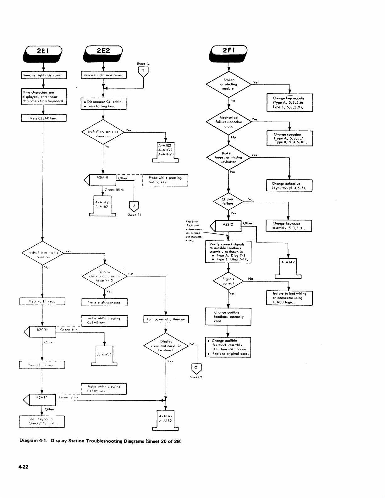
Sheet
26
No
.r--
........
----,
- - - - - -
Other
...--------..,
Probe
foiling
while
key,
pressing
Change
keybutton
defective
(5.3.5.5).
No
R~d
81'llk
IEcK:h
(Imp.
dlph~'vme'
Ie
kfl'Y
pr
..
~st!d
dno
character
Pro
hE>
whilp
fA"
key.
Nhilp
"'y
["e~\i"g
orp,>:.;"o
CfAR
Pro~)e
(I
Diagram 4-1. Display Station Troubleshooting Diagrams (Sheet
4-22
20
of
29)
Sheel9
•
Chonge
feedback
•
Replace
if
foilure
audible
assembly
still
original
occurs
cord.
.
Page 50

s •• parograp!.
descriptian
and 8
••
ybaarda.
5. 1 .•
for
~
Type
A
No
•
Type
A-
Chong"
keyboard
ossembly
(5.3.5.3\.
e
Type
8-
Chonge
circuit
board
(5.3.5.11).
No
Other
Probe
character
lost
position.
while
in
ent
ned-to-
...
ng
Yes
Yes
No
Diagram 4-1. Display Station Troubleshooting Diagrams (Sheet 21
of
29)
I •
~r:o~~s;:~:=~d
I
15.3.5.
I\,
I • Remove top
I
I •
I battom pon
cover
(5.3.5.2\.
::=~~~;!:,rd
(5.3.5.3).
Troubleshooting
Diagqms
~23
Page 51
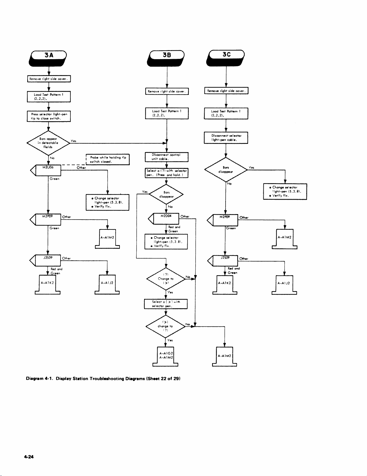
Other
Probe
switch
e
Chonge
light-pen
e Verify
while
closed.
holding tip
selector
(5.3.81.
fix.
Diagram
4-24
4·1.
Display Station Trouble.hooting Diagrams (Sheet
22
of
291
Page 52

• Model 1-Remove left
side
cover.
• Model 2-Remove front
cover.
• Unplug
lin.
cord
source.
-PULL
from
switch.
power
• Pull
OFF
e Set ohmmeter on X 1
range.
• Mealure resistance
across line cord plug.
Ves
Ves
Sheet 2
e
Turn
power off.
• Change
analog
(Mod
1,5.3.3.3
Mod
2,
5.3.3.4)
• Power on and
(5.2.1)
cord.
adiust.
e
Change,
in following
order:
1.
PC
board
(5.3.2.1).
2.
AC
capacitor
(5.3.2.3),
3.
Ferro transformer
1,5.3.2.6,
(Mod
5.3.2.7)
Mod
2,5.3.2.8,
unit
5.3.2.9)
installed.
• Check for repair ofter
each
Ves
No
No
ug
2-wire
connector
P2
on bock
pow.r
pi
ns
5.3.2.6,
5.3.2.7
5.3.2.
bal(.
of
pi
ug
range.
of pri mary
• Measure resistonce
ocross
removed.
• Ohmmeter on X 1
Change ferro transformer
1,
(Mod
Mod
2,5.3.2.8
Yes
• Turn power
e Remove plugs
e Change fuse F 1 •
•
Change line
and
pow.r
Tum
P4
bOl(o
pow.r
from
off.
prime
on.
cord.
P2
Ves
•
Ch.ck
prime power
• Change prime powerbox
(Mod
1,
5.3.2.4
Mod
2,5.3.2.5)
• Change fuse
•
Reconn.ct
Fl.
all
conn.ctors.
bOl(
if
and
no
connectors.
shorts
or.
evident.
•
Turn
power
power
board.
1,
5.3.2.6,
5.3.2.7
2,5.3.2.8,
5.3.2.9).
off.
plug
P2.
Fl.
on.
off.
P1
from
Fl.
Fl.
connectors.
•
Reconn.ct
• Change fuse
• Turn power
•
Turn
• Reconnect plug P4.
•
Remove plug
PC
• Change fuse
• Change ferro transformer
(Mod
Mod
• Change fuse
• Reconnect all
No
No
•
Ch.ck
cord
connectors.
• Change cord
no shorts are
• Reconnect all
Sheet 25
reader
reader
evident.
connectors.
and
if
Diagram 4-1. DispilY
Stltion
Troubleshooting Dillll'llmi (Sheet
23
of
29)
Troubl ..... ooting Diagrams 4-26
Page 53
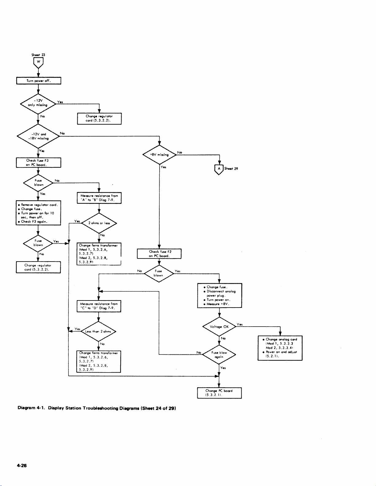
Sh
• Remove
regulator
•
Change
fuse.
• Turn power
sec,
then
•
Check
F3
•• t 23
on
off.
again.
No
V.s
card.
for 10
Change
ferro tronsformer
(Mod
1,
5.3.2.6,
5.3.2.7)
(Iv'tod 2,
5.3.2.8,
5.3.2."
Change
(Mod
5.3.2.7)
(Mod
5.3.2.9)
__
ferro transformer
I,
5.3.2.6,
2,5.3.2.8,
---1
Diagram 4-1. Display Station Troubleshooting Diagrams (Sheet
24
of
29)
•
Change
• Disconnect
power
• Turn power
• Measure +
No
Chonge
(5.3.2.
fuse.
plug.
Ves
PC
11.
analog
on.
8V
board
.
Ves
•
Change
onalog
1,5.3.3.3
2,
5.3.3.4\
on
and
card
adjust
(Mod
Mod
• Power
(5.2.11.
4-26
Page 54
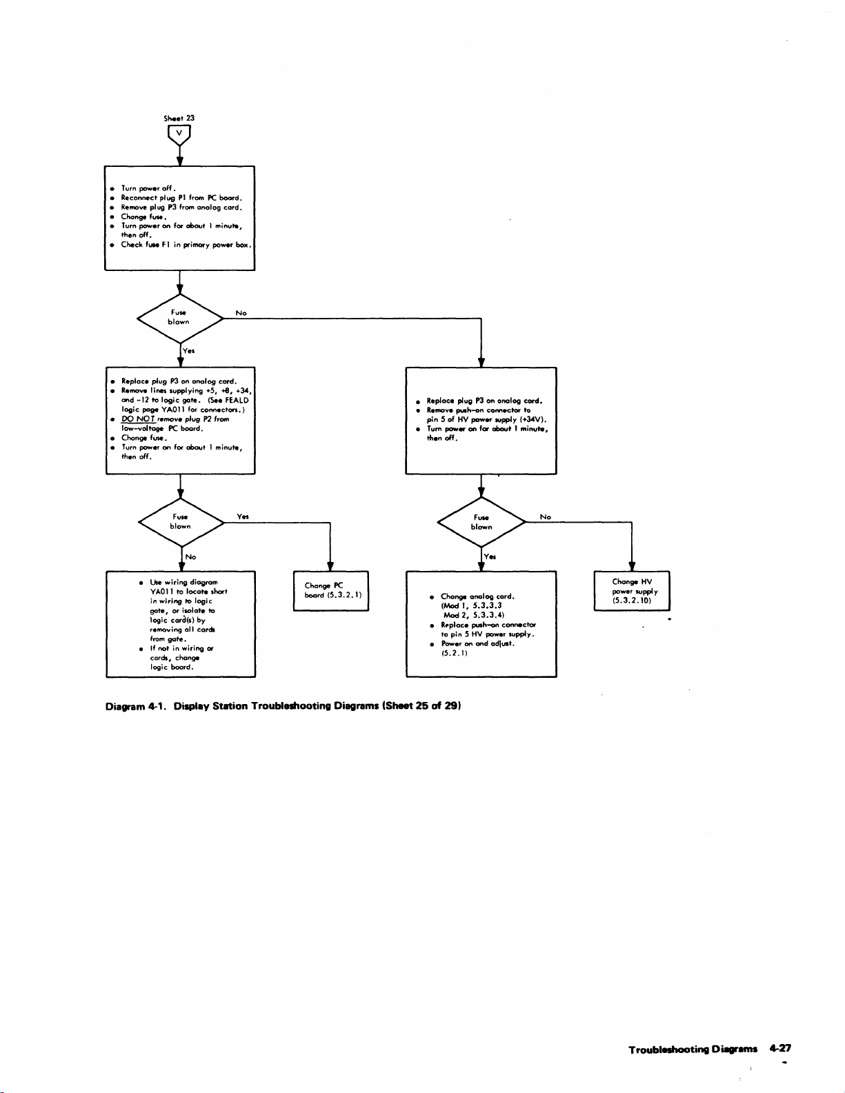
Sheet
23
• Turn power
• Reconnect
• Remove plug
• Change f
• Turn power on for
•
• Replace plug
• Remove lines supplying +5,
•
• Change fuse.
•
.....
then
off.
Check
flMe
and
-12
to
logic
page
DO
NO T remove plug
low-voltage
Turn
power
then off.
•
Use
Y
AO
in
gote,
logic card(s) by
removing
from
•
If
nat
cards,
logic
off.
plug
PI
from
P3
from
about I minute,
F 1 in primary
P3
on
analog
logic
gate.
YAOll for
PC
board.
on
for
about 1 minute,
wiring
diagram
11
to
locate
wiring
10
logic
or ilOlate 10
all
gate.
in wiring or
change
board.
analog
connectors.)
P2
cards
PC
paw.r
(See
short
board.
card.
-+6,
from
card.
box.
No
+~,
FEALD
Yes
Change
board
PC
(5.3.2.1)
• Replace plug
e Remove
push-an
pin 5 of
e Tum pawer
HV
then
off.
•
Change
(Mod
Mad 2,
•
R~place
to
pin
e Power on
(5.2.ll
1,
P3
on
connector
power IUpply
on
for
about 1 minute,
analog
card.
5.3.3.3
5.3.3.4)
push-an
5 HV pawer
and
adlUlt.
analog
connector
supply.
cord.
to
(+~V).
No
Change
pawer
suppl
(5.3.2.10)
HV
y
Diagram 4-1. Display
Station
Troubleshooting
Diagrams
(Sheet
25
of
29)
Troubleshooting
0 iagrams 4-27
Page 55

•
Verify
functIons
• Swap
cobl.
good
all
offline
are
coaxIal
wIth known
devic
•.
correct •
sIgnal
Yes
Yes
Diagram 4-1. Display
Station
Check
cooxial
connector
coble
to
input
Troubleshooting
from
board.
Diagrams
(Sheet
26
of
29)
Page 56

No
• Reseat ex>nnector.
•
Check
card
operations.
• Return to
reader
customer.
Check
connector.
that
card
reader
e Press
and
•
Feed
RESET,
RESET
test
keys.
card
No
CLEAR,
into
Yes
Sheet
28
---------,
Pins for
next
identified
reoder
coble
assembly.
Measure
resistance
A 1
and
A2
cable
plug for
approx
imote Iy
Check
display
power
cabling
reader
ex>nnector
transformer.
by
150Hz)
reoder
between
of
check
numbers on
plug
reoder
400
station
from
motor
to
are
pins
ohms.
card
ferro
- - - - -
No
Yes
--
Measure
resistance
and
10
cable
approximately
Refe'
10 Reode-;::MOtorized
Theory-Maintenance-
Par~
Diagram 4-1. Display Station Troubleshooting Diagrams (Sheet
reoder
between
24
of
plug for
to
IDR-M
Catalog.
27
motor
reoder
400
of
pins
ohms.
29)
Troubleshooting Diagrams
4-29
Page 57
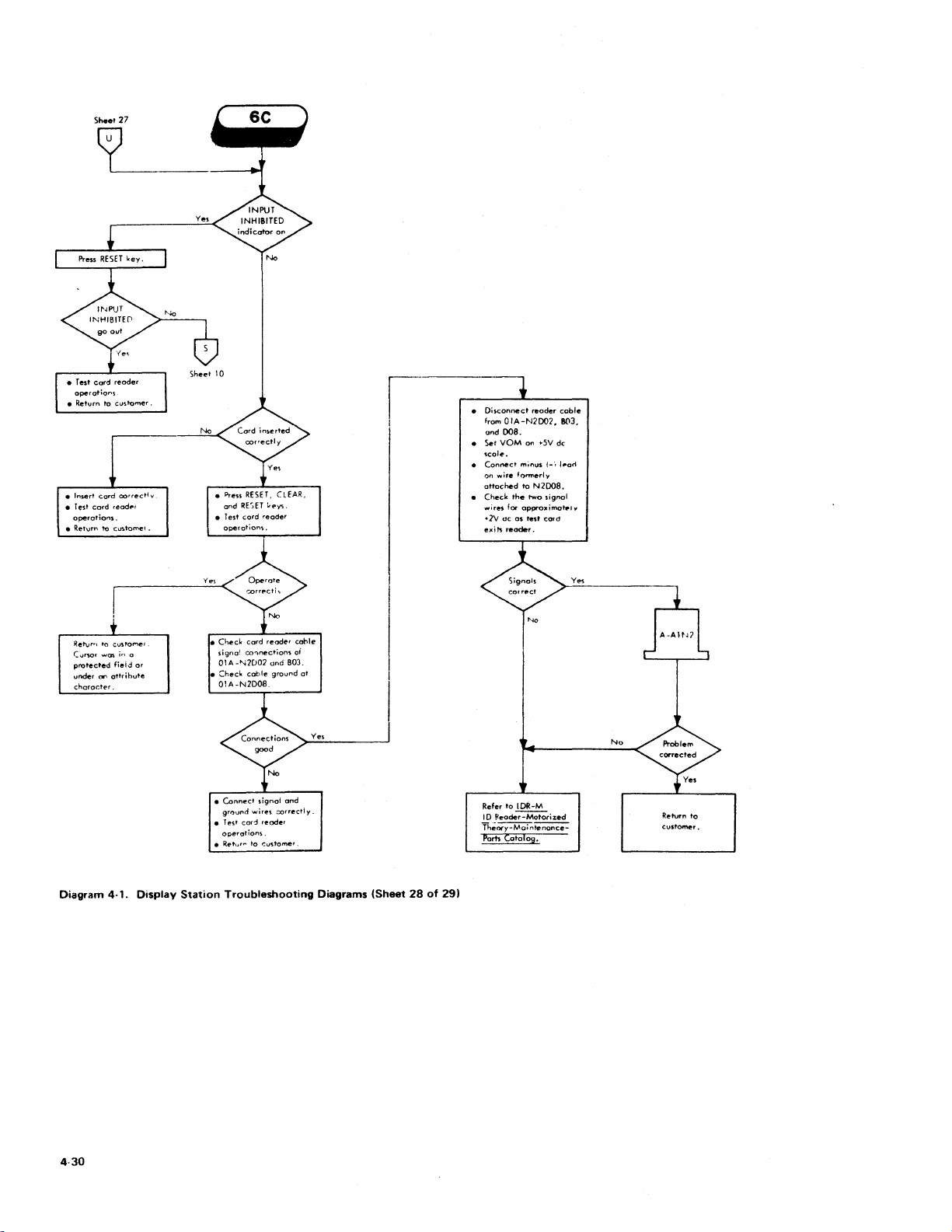
Sheel27
operotiOr"5
• Relurn 10
• Insert
• T
...
sl
cord
operations.
•
Retvf"
C(
cu,tomer.
card
corrC!ctly
read
.. ,
to
customet.
No
• Press
and
•
Jesl
RESE
RE,ET
cord
No
T,
CL
~eY'.
reoder
EAR,
I
I
•
Disconnect
from
and
•
Set
•
Connect
on
attached
•
Check
wires
.]V
I!xil'!
OIA-N2007,
008.
VOM
minus
wire
formerly
to
Ihe
for
approximateI
ac
as
reader.
reader
on
N2008.
two
lest
.5V
cord
de
1-"
signal
cable
8(\3,
l~ac1
v
Retvrq
Cursor
prolected
under
character.
Diagram
to
was.
CW'I
cvstoMef.
in
fiei.:!
attrihute
4-1.
a
or
Display
•
• :::heck
Station
Check
cord
co!')nections
coble
Connect
grl)vr'ld
Te,t
cad
operations.
wires
to
reader
and
signal
reade'
cudome
ground
.::orredly.
signa!
0IA-"<2D07
01A-N2DOB.
•
•
• Returr'"
Troubleshooting
B03.
and
cohle
of
r
.
01
Ye,
Diagrams
(Sheet
28
of
29)
Refer
10
IDR-M
ID
~"ader-Motorized
Th';~~
Ports
Catalog.
Ye,
No
Return
customer.
to
4-30
Page 58

Turn_oil
lie
Mealure ,
~
A/F2-B Mod I
01C1F2-B Mod 2
No
.......
+34V
....
tarec:.
CII
....
In
10110"'",
otdo<'
I
LVPC
Boord
(5.3.2.11
2.
Ferro transformer
(5.3.2.615.3.291
o..ck
for repeir after
..
chstep.
F
.....
0<
With
ohmme'.'
keybo.rd
tln\e
until
21124
to
connector
one.,
Short
c.rd.
stili
connected. remove
co,dsiftOIA/A1.nd
the
OIA/Al
•
ISOI.ted
or board
IS
connector
In
R
........
10<30
T ..
,n_on
tu,n
_
34VI
......
Chock In
ohm
.....
'.
__
_
oil.
ChocIl
'n_
Chongo
In
10110wt'"
ordlr.
1 An.IOIIcord
2.
HV
go
....
a.c:k
for
f'ePIi"
ooch '
...........
CIIocIIend,_rr
3CV
wi"",
L'o'_,suppiV
CirCUit boarel
t
...
hoidet. s..
1000IcPIfIOVAOII
for
WIr'
routine
, s .. pplv
.fte,
nl.
from
to
fol1owl",
o,do<
1.01A/A1M2cord
2
34
V
WIring
from
tu
..
10
boord. s..
1000Ie
pogo YAOII
wire
routine.
3 34'0'
ont'v
on
It
0IA/A1K8B04
bGo,d
fo'
Troubleshooting
Diegrams 4-31
Page 59

Section 5. Checks, Adjustments, and Removals
This section contains all alignment, adjustment, and
removal procedures
Display Stations.
checkout procedures
required and
to
nece~ry
to
maintain
IBM
It also contains service checks and
to
determine whether adjustments are
verify
the
accuracy
of
any adjustments
3277
made.
5.1 CHECKS
5.1.1 Display Station Test Using Test Pattern 1
A comprehensive test
features
is
performed
the procedures described
step-by-step procedures describe
various operations should be performed and
of
expected
each operation.
The tests should be performed
presented, because each test
the
screen from preceding tests. The observations described
in
paragraph 5.1.1.1 apply
testing depends on what features are attached
of
the
display station and
by
using diagnostic Test Pattern 1 and
in
the
following paragraphs. The
the
sequence
all
in
which
attached
the
in
the sequence
is
dependent on data left on
to
all display stations. Further
to
the
the
results
display
station.
If a problem
ational test, refer
shooting Diagrams
5.1.1.1 Initialization and Observations
1.
Load Test Pattern 1
is
discoverect while performing this oper-
to
the
to
Symptom I ndex or
resolve
the
problem.
on
display station being checked.
the
Trouble-
(See paragraph 2.2.1 for instructions for loading Test
Pattern 1.)
that
should
SYSTEM AVAILABLE
be
on
after
pattern
is
the only indicator
is
loaded.
2. Take display station offline by removing control unit
signal cable. Jack
under front cover. Do
removing cable
3. Compare image
is
located at front of display station,
not
turn
power off while
or
Test Pattern 1 wi" be lost.
on
screen with expected image shown
in
Diagram 2-4. The "NON DISPLAY" field should be
blank.
Top
two
rows are displayed
next two rows are displayed
is
of last row
displayed
4. Check for only
character position
in
high intensity.
one
cursor. Cursor should be
of
second row
5. Check quality of displayed image.
or
tilted
blurred, and characters should be formed
in
normal intensity,
in
high intensity, and half
of
displayed data.
Image should
in
not
first
be
properly with correct inter-row spacing.
6. Vary Brightness
control. Set it where high intensity
characters have proper brightness.
7. Vary Contrast control.
characters contrast with high intensity characters
Set
it
where normal intensity
at
desired level.
5.1.1.2 Security Keylock
1. Turn security key
disappear from screen,
should
light, and cursor should remain displayed.
2. Turn security key on. Original data should reappear
5.
1.
screen,
and
1.3 Tests
INPUT INHIBITED indicator should go
from
Test
(Optional Feature)
off
(vertical position).
All
INPUT INHIBITED indicator
Keyboard (Optional Feature)
data should
on
out.
Press the RESET key. The display image should appear as
shown
character C
indicators should
in
Diagram 2-4, with
in
the
second row of displayed data.
be
on.
1.
Key
in
the
row
of alphabetic characters and
space exactly as they appear
the
cursor located under the
in
the row above.
the
No
one
All
characters should enter correctly, and cursor should
move under
2.
Move
data, using
3. Press
I after Space bar
cursor under C of
~ (Right) key.
INS
MODE
key. INSERT
is
pressed.
CK
in
second row of displayed
MODE
indicator should
light.
4. Press A key. Field should now appear
A~K.
5. Press FIELD MARK key. (Use B key on Ope.ator
Console keyboard.) Field should now appear
A;
~K
(AB£K).
6. Press C key. The data should
not
change,
but
the
INPUT INHIBITEQ indicator should come on (in
addition
INSERT
MODE
indicator, which has
to
the
remained on.)
7. Press
8. Press DEL key. The
9.
RESET key. Both indicators should
C should disappear, and the field
A;~
should now appear
(AB~)'
Press +-I key (New Line). Cursor should move under C
character
in
fourth row of displayed data.
10. Enter the special characters as they appear
go
out.
in
the row
above, shifting where required. Cursor should appear
under 0 character after last special character enters.
11. Enter
the
digits 0 through 9 and the characters, . - and
A as they appear
in
the row above.
keyboards, use the , over
(On
Data Entry
* and . over $ keys
to
enter
the , and . characters.) The following results should
occur:
a. Typewriter and
out
numeric lock feature -
Operator Console keyboards with-
all
characters should
enter.
Checks, Adjustments, and Remova.. 5·1
Page 60

b. Data Entry keyboard without Ilumeric lock
feature -
characters,
character enters as
c.
All
keyboards with numeric lock feature - char-
acters . and -
lock and
INPUT INHIBITED should light
and A keys are pressed. (Use Reset and
. and - entpr .nnrrnally; the A
< symbol.
enter
normaHy; keyboard should
when,
-+
keys to
move cursor from those positions.)
Check t (Up),
12.
'"
(Down), and ~ (Backspace) cursor
move keys for proper operation.
Check
the
13.
other
in
the
Typamatic function of
key with Typamatic.capability. Use
fourth row
of
displayed data for this step.
14. Move cursor under first character displayed
the
Space bar
the
or
any
first field
of
test
message.
15. Press any alphameric key.
tor
should come on, and character should
display because field
INPUT INHIBITED indica-
not
enter
is
designated as a protected data
or
field.
16. Press
17. Press ENTER key. INPUT INHIBITED indicator
RESET key. INPUT INHIBITED indicator should
go
out.
should light, and keyboard should lock.
18. Press
RESET key. INPUT INHIBITED indicator should
go
out,
and keyboard should unlock.
Note: The following steps check tab, DUP, and new
line functions.
~
19. Press
character A
20. Press
position, and cursor should move under
(On
should move under
should
21.
Space one character position. The I should disappear.
22. Press
space
23. Press Tab key.
boards.) The cursor should appear in
position of
(Tab) key. Cursor should appear under
in
second row of characters.
DUP
key.
An
asterisk
(*)
should appear
in
cursor
I of INSERT.
Operator Console keyboard, use Tab key; cursor
I of INSERT,
not
appear.)
t+- (Backtab) key. Cursor should move back one
to
where
the
I was formerly located.
(Use
SKIP key on Data Entry key-
the
fourth row of displayed data.
but
the asterisk
the
first character
Note: The following steps test the erase and clear
functions.
in
24. Position cursor under character E
second row of
displayed data.
25. Press
26. Press E
27. Proceed
ERASE EOF key. Characters E through Z should
not
disappear, and cursor should
RASE I NPUT key.
including keyed-in characters and field
appeared as
INSERT CK, should disappear from screen.
to
paragraph 5.1.1.4 if display station being
tested has a selector light-pen attached.
move.
All
unprotected data,
that
If a pen
originally
is
not
attached, press CLEAR key. All characters remaining
on
screen should disappear, and cursor shou'd reappear
in
first character position
in
first row. Press RESET
key.
to
28. Proceed
operator identification card reader attached.
reader
off, and reconnect control
5.1.1.4 Selector Light-Pen Tests (Optional Feature)
1.
Fire pen on detectable field
as its first character. Question mark should change
greater-than
paragraph 5.1.1.5 if display station has an
is
not
attached,
(»
symbol. Remainder
test
is
completed. Turn power
unit
signal cable.
that
has
c:J
Question mark
of
field should
If a card
to
not
change.
2.
Fire pen again on the field. The greater-than symbol
to
should change back
not
field should
change.
3. Fire pen on next detectable field
a Question mark. Remainder of
that
has a greater-than
symbol as its first character. The greater-than symbol
to
should change
not
should
4.
Fire pen again on same field. Ouestion mark should
a Question mark. Remainder of field
change.
change back to a greater-than symbol. Remainder of
Id
not
field shou
5.
Press CLEAR key.
disappear, and cursor shou
O.
Press RESET key.
6.
Proceed
change.
All
to
paragraph 5.1.1.5
characters on screen should
Id
move
to
character location
if
display station being
tested has an operator identification card reader
attached.
a card reader
is
not
attached, test
If
completed. Turn power off, and reconnect control unit
signal cable.
5.
1.
1.5
(Optional Feature)
1.
Key
in
2.
Return cursor
Operator
a few characters
Identification
on
the screen.
to
character position
Card Reader
1.
(Do
not
Tests
use
CLEAR key.)
3. Read
card reader test card
(PN
2143816). The
in
following events should occur:
a.
Keyed-in data disappears from screen.
b.
Cursor moves
c.
INPUT INHIBITED indicator comes on and stays on.
If
cursor does not move
u nsuccessfu
4.
Tests are now completed. Turn power off, and reconnect
40
character positions.
40
spaces, read-in operation was
I.
control unit signal cable.
Display Station Operational Test (without Test
5.1.2
Pattern 1)
Quick
The following test sequence is a
that
can
be
used
as
an offline display station reliability test.
This procedure tests
is
not
as
but
comprehensive as the procedure described
display station circuitry extensively,
checkout procedure
paragraph 5.1.1. It can be used as a Quick checkout to
is
verify correct operation after maintenance
performed.
(7)
a
is
in
5-2
Page 61

Perform
2.
3.
4. Press
5. Exercise
6. Press several alphameric
7. Key in a
8.
9.
10. Exercise
11. Move
12. Backspace
the
steps
in
sequence
1.
Turn
power
off.
Take
display
cable
from
front
of
for
access
Turn
appear
should
-+ (Right) key,
move
through
reaching last
in first
station
display
display
to
it.
power
on
screen
be
lighted.
character
character
offline
station
station.
on.
Within
at
character
and
each
character
location in second row.
t (Up), + (Down), +-' (New Line),
(Left)
performs
ponding
move
character
character
Press
cursor
Exercise
Observe display screen as each
that
meric
just
cursor
one
an
location,
proper
cursor
move keys. Observe
its
operation
characters
space as
complete
of
row
position
correctly.
should
each
row
enters,
of
next
alphameric key. Char.acter
and
cursor
both
upper
characters
Typamatic
into
enter.
function
last row,
chararacters.
cursor
near
entered.
for
most
by
I/O jack.
Front
15
location
hold it
location in
location,
keys
in succession.
display,
new
character
of
cursor
row.
should
and
lower
of
and
middle
effective results.
removing coaxial signal
cover
seconds,
down.
cursor
characters. When last
should
advance
shift
key
is
each
key
of
group
13. Press INS MODE key. INSERT MODE
light.
14. Press
right
to
first row.
15. Press
enough
of
cursor
to
move
RESET key. INSERT MODE
to
times
end
to
of
cause
row
indicator
Space
bar
out.
16. Delete several
cursor
same
row
character
17. Move
18. Press
19. Press
20.
21.
cursor
ERASE EOF key.
tion
through
cursor
should
ERASE INPUT
and
cursor
Enter
several alphameric
If display
key
off.
INPUT INHIBITED
characters
position
at
should
right
position each
to
middle
last
not
should
station
Characters
of
time
of a row
position
move.
key~
move
to
has
the
should
should
using DEL
disappear,
cursor
should
DE L is pressed.
of
Characters
on
screen
All
characters
location
characters
security
key
disappear
light,
characters.
O.
as in
and
remain displayed.
Turn
22.
security
screen,
key
on.
and
INPUT INHIBITED
Original
data
should
should
Jack
is
located
must
be
removed
cursor
O.
the
No
indicators
Cursor
row.
should
should
should
After
appear
and
that
each
The
corres·
and
cursor
should
appears.
appear
should
appear
one
of
all keys.
in first
space.
pressed, checking
Typamatic
in
several alpha-
of
indicator
key.
characters
should
characters
and
wrap
around
should
key.
Character
and
characters
move
left
from
cursor
posi-
should
step
lock
erase,
should
6.
feature,
from
cursor
erase,
turn
screen,
should
reappear
go
out.
at
+-
key
in
at
go
in
in
one
and
on
23.
Press
CLEAR
should
reappear in
24. Press Backspace
25. Press
26.
sound
If
an
any
when
operator
proceed
control
27. Press
unit
CLEAR
alphameric
Return
28.
29. Read
30.
Observe
cursor
from
31.
If
cursor
in
moves
screen as
cursor
key,
disappear
from·
character
key
two
character
key
key.
is
pressed if
identification
to
step
27.
signal
cable
key,
characters
to
location 0 using +-(Left)
card
reader
test
that
INPUT INHIBITED
40
spaces,
card
passes
does
not
move
then
RESET
screen,
location·
times.
Audible
Turn
if a
RESET
as in
step
card
and
through
40
O.
feature
card
power
card
key,
6.
(PN
keyed-in
spaces, read-in
was unsuccessful.
32.
Offline
reconnect
5.1.3 Voltage
A
ferroresonant
and multiple secondary
voltages. (World
ferro
protected
is
located
consist
CRT
LV
tests
are
completed.
control
unit
signal cable.
Clecks
transformer
Trade
with a tapped
(ferro) with a
taps
provides
Corporation
primary winding.)
by fuse F 1 in series with its
in
the
prime
power
box.
of
low dc voltages, high dc voltages,
filament
printed
voltage. These voltages
circuit
(PC)
board
or
(TB1).
to
the
+8V
screws
Symptom
is
DC
and
on
the
Refer
Diagrams if a voltage
5.1.3.1 Low-Voltage
Modell:
the
For
capacitor
Diagram 7-9 shows
capacitor screws. Remove
the
circuit
board.
For
+5V
at
the
fuse holders
at
A/F
Index
incorrect
or
Checks
-12V, measure
the
LV
location and
the
left side cover
and
+34V, measure
1-B
for +5V
(Diagram 7-3).
Model 2:
through
printed circuit
designates
voltage.
fuse holders
For
+8V
the
access holes
the
For
+5V
at
and
board.
A line with
pairs
of
and
+34V, measure
01C/F
1-8 for +5V and
-12V, measure
in
the
terminals associated with
(Diagram 7-E). Diagram 7-10 illustrates
Remove
the
following voltages can
the
Observe
correct
front
cover for access
the
polarities
test
leads
of
the
to
prevent damage
be
measured
to
terminals,
at
key. All
and
cursor
alarm
(feature)
is installed.
reader
off,
reader
then
and
is
is
not
enter
key.
2143816).
indicator
data
reader.
Turn
power
110V
all
display
display
stations
The
primary
Display
winding. F 1
station
and
can
be
checked
at
Terminal Board 1
and
Troubleshooting
is
missing.
the
low
dc
printed
the
circuit
polarity
for
and
A/F2-B for +34V
the
low
shield
that
arrowheads
the
voltages
01C/F2-B
the
PC
board
the
circuit
and
to
the
the
PC
board:
characters
should
should
attached,
reconnect
attached.
several
comes
on,
disappears
operation
off,
and
ac
primary
station
use a
ferro
voltages
6.3V
at
voltages
board.
of
access
the
voltages
dc
voltages
covers
at
each
end
each
at
for
+34V
shield.
board.
probe
with
meter.
The
is
ac
the
at
the
to
the
the
Checks,
Adjustments,
and Removals
5-3
Page 62

+5V ± 1 0%
+8V ±12% (This voltage
+34V
-18V (This voltage
-12V ±4%
5.1.3.2 High-Voltage Check
The
only
high voltage
dc
(which
voltage
should
supply,
with
circuitry
1.
2.
3.
4.
5.
is
is
correct,
also
it
is
the
standard
whenever
Turn
power
Set
voltmeter
measure
Connect
terminal.
Connect
terminal
back slightly.
Turn
power
6. Check
(Because
impossible
with
the
is
given.) If voltage
test
leads
circuitry
proceed
7.
Turn
power
8. Remove push-on
terminals 1
9.
Turn
power
10. Check again for
voltage
from terminals,
nectors,
(paragraph
the
HV
5.1.3.3 Arc-Suppression Check
A defective arc-suppression
tive HV
experienced
power
(This
voltage
A/F 1 (Modell)
(Model 2) Diagram 7-5.)
PC
board.)
±10% (This voltage
A/F2
(Modell),
(Model
PC
regulator
-12V will also
be
for a meter
power
2),
Diagram 7-5.)
is
fuse-protected
board
derived
corre~t.
impossible
off.
up
to
minus
plus (+)
2 (Diagram 7-14)
on.
this
to
IBM
from
(paragraph
with
off.
and
on.
is
correct,
and
5.1.3.3).
supply
with
and
card.
be
that
from
the
other
Because
to
obtain
voltmeter.
HV
troubles
selector
+400V
measure
meter;
steps 7 -10.
either
(-)
meter
voltage
is
term
ina
connectors
2.
+400V
turn
reconnect
check
supply
or
dc.
meter
indication
therefore,
correct,
5.1.3.3).
If
(paragraph
analog
of
If
missing.)
should
the
switch
is
the
Is,
the
voltage is still
circuit
the
is
protected
Diagram 7-3
is
protected
is
protected
Diagram 7-3
is
the
input
this
voltage
be
checked
HV power
high voltages
the
+400V
an
accurate
Check
occur.
lead to HV
by
a low-current
+400V
and
±50V
power
power
the
to a position
lead
on
sliding push-on
of
dc
the
wide range
turn
power
check
the
If
voltage
from HV
dc
off, remove
supply
arc-suppression
5.3.2.10).
may
card.
If excessive
two
assemblies,
by
fuse
and
01C/F
by
fuse
by
fuse
and
01C/F2
by
fuse
to
the
is
missing,
is
the
supply).
for
the
is a low-current
measurement
arc-suppression
that
any
dc
power
connector
+400V
on
appear
±50V
supply,
operating
of
off,
arc-suppression
is
incorrect,
power
terminal 2. If
test
push-on
circuitry
incorrect,
as a defec-
trouble
check
at
1
F2
on
at
F3
on
-12V
the
+400V
If this
CRT
will
return
supply
dc.
it
voltage
±50V
remove
supply
leads
con-
change
the
arc-suppression
circuitry
Diagram 7-15)
voltage
display
Visual Checks:
1. Check
2. Check
other
3. Check
showing
Model
1.
2.
3. With
4.
Model 2 Resistance Checks:
1.
2.
3. With
is
4. Replace voltage
arc-suppression
change
distribution
4,
the
5.1.3.4
The
voltage
determine
filament
The
5.3.3.2,
located
1.
2.
is
is
located
distribution
stations.
for
bent,
for
bent
components
for
obvious
1 Resistance Checks:
Turn
power
Remove
pins
specified:
Replace
not
Turn
Disconnect
minals 12, 13,
pins
specified:
not
If
if
troubleshooting
Turn
Set
measure
arc-suppression
the
on
and
E9
El0
and
correct.
power
the
on
the
12
and
14
and
correct.
the
above
the
the
checks
6.3VAC
CRT
filament
used
if
at
CRT
cone
steps
on
the
power
voltmeter
CE VOM,
the
the
CE YOM,
13
15
arc-suppression
board
the
6.3V
circuitry
on
broken
off.
arc-suppression
E13
E14
arc-suppression
off.
wires
voltage
- 1 Megohm
- 1 Megohm
checks
circuit
were
in
6.3V
back
shield
1-3).
LV
off.
ac.
as
on
Model 1 display
board
broken,
capacitor
and
could
capacitors
damage.
check
- 1 Megohm
- 1 Megohm
from
14,
and
check
distribution
distribution
do
and
(Model 2).
performed
diagrams.
Check
voltage
the
display
ac
is
of
the
must
This
PC
board.
selector
listed
below.
the
arc-suppression
(TB1, Diagram 7-11)
or
missing wires.
leads
cause
board
from
between
board
board
voltage
15.
between
board
board
not
reveal
if excessive
board
(Model
Return
as a
of
6.3V
station. A quick
present
voltage
CRT
be
removed
switch
is
ne~k,
is
Arc-suppression
stations
that
are
arcing.
or
other
its
socket.
the
following pairs
for
E7
and
E13 -Infinity
E7
and
E14
if
the
distribution
the
following pairs
for
13
and
16
14
and
16 -Infinity
if
the
an
obvious
trouble
1)
to
Diagram 4-1,
result
of
ac (±10%)
to
look
near
to
see
protected
to a position
board
(Zl,
and
on
on
Model 2
too
close
components
the
resistances
- Infinity
resistances are
board
the
resistances
- Infinity
resistances are
fault
in
persists,
or
the
voltage
sheet
instructions
is
the
only
check
for
a glowing
the
tube
socket.
filament
by
fuse F 1
that
the
to
of
ter-
of
the
in
ac
to
(par.
will
5-4
Page 63

3. Remove fuse
display stations.)
4.
Connect a meter
5.
Tum
power
6. Check
7.
Turn
power
holder.
8. Reinstall fuse
5.1.3.5 High-Voltage Power
1.
Turn
power
2. Remove HV
retu rn).
3.
Set
CE
4.
Measure resistance
4.
5. Reverse
6. Replace HV
step 4 or
5.1.4
Keyboard Checks
Two
different
Display Stations. Both are identical in
only
slightly in external appearance.
Type
II
A"
top
to
bottom.
are
slightly concave.
with
the
and
type
regulator (large
keyboard
circuit
of
corner
board,
the
circuit
a 24-pin SL T
of
the
circuit
of
Fl.
on.
for a meter
off,
and
off.
power
See
Diagram 7 -14.
VOM
selector
meter
leads
power
5 indicate a
style
keyboards
The
keyboard
of
cable
the
cover
cable
connection
transistor
plugs
and
the
board.
connector
board,
circu it board.
(Remove
lead
indication
and
shield (if removed).
between
keyboards
have
rows
The
regulator
The
and
shield
on
each
end
of
6.3V
remove
supply
switch
and
measure
supply
shorted
an
of
two
removed by observing
into
Type B keyboard
which
the
meter
Supply
leads 3 (UV)
to
RX10
HV
power
again.
(par. 5.3.2.10) if readings in
or
open
may
even slope
keys
on
types
and
the
on
heat
the
rear edge
is
located
is
mounted
regulator
of
Check
be
for
access
on
Mode! 2
fuse holder.
ac.
leads
from
fuse
and
4 (DC
position.
supply pins 3
condition.
found
on
IBM
3277
operation
The
rows
downward
Type
can be distinguished
location
sink).
in
in
is
located in
and
of
keys
"B"
keyboards
the
location
of
the
The
Type
of
the
printed
the
left
corner
cable plugs
the
left
corner
the
vary
from
+5V
into
right
and
on
A
tronics assemblv (Type B
device. Do
While performing
assembly'
that
A faulty
good
the
factory
marked
and year.
5.1.4.1 Voltages
Type A Keyboards
keyboard locations):
1. Check
(ground).
2. Check
(ground).
3.
Check
voltage
keyboard
power
+8V
Type 8 Keyboards (See Diagram
locations) :
1.
Check
(ground).
2. Check
terminals
assembly)
the
regulator
circuit board
correct
connector
+5V
not
should
could
cause
keyboard
one. A
faulty
if
on
Type
for
for
for
is
supply. Replace
dc
is
correct
for
for
meter
is
and
are
incorrect.
attempt
be
erratic
it
is
less
A keyboard assemblies by week
-12V
+8V dc between
+5V
dc
developed (by
assembly) from
-12V
+8V
(under
and
+5V dc
negative
+8V dc,
and
the
and
display
only),
to
repair any
the
following
visually inspected
operation
assembly
Type
A assembly
than
one
(See Diagrams 7-7
dc
between
across
keyboard
the
the
and
the
+5V dc is
dc
between
dc
on
one
the
circuit
on
the
(-)
lead
to
and
the
electronics assembly if
+5V
dc
station
and
the
audible response
other
checks,
for
shorts
or
erroneous
should
year
the
keyboard
KB
output
is
be
should
old.
The
and
KB 1 pins
KB1
pins V(+)
capacitor
voltage regulator
display
assembly if
not
correct.
7-19
for
Type B keyboard
1 pin
002
of
the
voltage regulator
board
other
terminal.
test
pin
008.
is
+5V
incorrect.
power
supply
keyboard
the
keyboard
or
results.
replaced
be
returned
date
7-8
for
Z(-)
station
(-)
and
electronics
Reference
Input
dc. Replace
the
+8V
Check
if +8V and
units.
grounds
with
to
code
is
(01-52)
Type
A
and
X
and
X
C1. This
on
the
+8V dc
the
and
008
to
the
dc
is
KB
a
1
The following paragraphs
which can be used
check procedure differs for
and B),
procedure
one
1. External
2. A FRU in
3. The
I
Problems external
outlined in
include
support
I
the
is
of
three
to
keyboard
circuit board with key modules; Type B assembly
consists
key modules
of
the
keybuttons,
modules (Type A
to
isolate
differences are
used. Keyboard problems can
possible areas:
the
keyboard.
the
keyboard.
assembly. (Type A assembly consists of
circuit board
in
an all-keys assembly.)
to
the
Troubleshooting Diagrams. Keyboard FRUs
switch modules, spacebar assembly,
contain
keyboard
the
different
noted.
and
electronics assembly with
keyboard
only).
check procedures
problems. When
keyboard
Ensure
that
be
should be diagnosed
circuit board and elec-
types
the
correct
isolated
the
(A
to
as
5.1.4.2
Correctly
(2.5V dc minimum)
encoder. With
encoder
character
s;gnal
only
it
if
Strobe check:
Key
Only
functioning
generates
output.
is
generated properly, and
two
inputs
is
found
to
the
encoder
1. Set
selector
will
accurately measure
2.
Place minus
3.
Place plus
Module and Encoding - Type A Keyboards
(Diagram 6-11)
two
to
be
defective. Replace
or
the
switch
(-)
(+)
key
modules
input
lines
and
only
two
the
strobe
This
procedure
the
encoder. Replace
printed
meter
meter
circuit
on
vol
t-ohmmeter
5V
dc.
lead
on
lead
on
Checks, Adjustments.
present
to
the
keyboard
active
inputs
signal
checks
the
key
the
keyboard
board
KB 1 tab
KB 1 tab R (strobe
two
present,
and
the
that
the
modules
the
key
is
defective.
to a position
X (ground).
and
Removals
active
assembly
the
encoded
strobe
activate
module
assembly
that
signal).
5,),)
if
Page 64

4. With no keys pressed,
2.5V. If the
step
7.
meter
5. Press and hold one alphameric key.
indicate less than 0.6V.
hi~er,
replace
the
meter
should indicate
indicates 0.6V or lower, proceed
The
If
the
meter indicates 2.5V
the
keyboard assembly.
meter
at
least
should
6. Press and hold two alphameric keys simultaneously.
The
meter should indicate
paragraph 5.1.4.3
O.6V
(or
lower)
7. With
meter
if
the
with
no
keys pressed:
leads attached
alphameric keys simultaneously. If
0.6V
or
lower, replace keyboard assembly.
8. Probe
KB1
pins
D,
E,
and Parity, Diagram 7-8) with
9.
Note
bit configuration
probe, a red indication
is
a 0 bit. With voltmeter, greater than 2.5V
and
less
than 0.6V
10. Find code
in
is
a 0 bit.
Diagram 6-5
configuration observed
11. Check center
module
be
removed from
for
two
lead frame terminals
2.5V
or
higher. (Keyboard assembly must
bottom
at
least 2.5V. Proceed
preceding results are correct.
as
in
steps 2 and
F, H,
J,
K,
L,
M,
no
keys pressed.
of
encoded
is
a 1 bit, and a green indication
or
6-6
that
in
step 9.
3,
press
meter
indicates
and N (bits
output.
With logic
is
corresponds
of
suspected
a 1 bit,
pan for this voltage check.
two
0-7
to
See paragraph 5.3.5.3.)
is
12. Replace defective module if 2.5V or higher
both
on
13.
If only
measures 0.6V
center terminals in
one
terminal measures 2.5V
or
less, recheck steps 8 through 11.
step
11.
or
measured
higher and
other
same results are obtained, replace keyboard assembly.
14.
Replace keyboard assembly
measured
in
step 11.
if
less
than
0.6V
3. Compare bit configuration observed
to
configuration for desired character shown
in
6-5 or 6-6.
or
5.1.4.4
Two SHIFT keys and
NUM
to
input signal
encoder generates upshift character codes
appearing
Shift
Key
Modules - Type A Keyboards
LOCK keys on
to
the keyboard assembly encoder. The
on
the
top
the
shift LOCK key (NUMERIC and
data
entry
keyboards) generate an
of
half of
the
keyboard keys. The
following procedure isolates a shift module failure.
1.
Set
bit
volt-ohmmeter selector switch
accurately measure
2.
Place minus
3.
Check
all
(minimum) on both
up
to
+5V dc.
(-)
meter lead on
three shift keys individually for 2.5V
center
key module when each key
(maximum) when key
4.
Replace shift module
on
both leads.
5.
If shift module generates proper levels, and keyboard
is
restored.
that
fails
to
a position
KB 1 tab
leads
X (ground).
of
the corresponding
is
pressed and for
to
generate
generates incorrectly shifted characters (5.1.4.3), replace
keyboard assembly.
5.
1.4.5 Spacebar Assembly Mechanical Checks
The spacebar assembly and mountings should be checked
for easy motion and freedom from binds. The spacebar
should depress and return
drag
or
If
binds. Replace
broken mountings,
may
not
is
(actuator) if
be necessary
the
problem
or
to
the restored position
the
spacebar assembly if binds,
bent
components are discovered. It
to
replace the spacebar module
is
mechanical.
step
in
Only
the
characters
proper
2 with
Diagram
that
will
O.6V
levels
without
5.1.4.3
The unshifted and shifted codes for
Output
Codes
a"
keys
on
both
type
keyboards can be checked by the following procedure,
which uses the logic probe and
1. Press and release desired key. Hold
on
data
entry
keyboards) key down while pressing key
desired character
is
on
Diayram 6-5, 6-6, or 6-7.
SHIFT
top
half
of
keybutton.
(NUMERIC
2. Probe pins listed below with logic probe, and note bit
configuration observed. A red
and a green
5-6
Pin
(lA
S05
S08
S09
S02
U05
M10
U09
M11
S13
(DOWN)
1-B2)
indication
(UP}
indication
is
a 0 bit.
Keyboard
0
'}
..,
oj
4
5
6
7
Parity
Bit
is
a 1 bit,
ADJUSTMENTS
5.2
Adjustment procedures for the
should be performed after it
IBM
is
established
3277 Display Station
that
all
voltages are correct. Paragraph 5.1.3 details
checkout procedure.
if
5.2.1
Display Image Adjustments
A test pattern generated by the diagnostic program provides
the display image
Pattern 2
is
Test Pattern 3
The procedure for displaying
described
pattern
from
is
the
in
not
to
be used during image adjustment. Test
used
to
adjust
the
Model 1 display image, and
is
used
to
adjust
the
Model 2 display image.
the
required test
paragraph 2.2.
used,
the
If
the program-generated test
test
pattern image must be keyed
keyboard. Diagrams 2-5 and 2-6 show Test
Patterns 2 and 3, respectively.
Adjustments should be performed
However, if only minor
touchup
in
the sequence listed.
adjustment
analog card adjustments can be made separately. Use
operating
the
voltage
pattern
is
required,
is
in
Page 65
Diagrams
specified in the
equipment
7-1
throu~
is
required.
following
AI ignment mask:
Model 1 -
Model 2 -
PN
PN
Screwdriver (small blade)
T backpanel jumper
SL
5.2.
1.
1 Brightness
The Brightness control
Note:
OF F-PUSH switch.
7-6
to
locate the adjustments
procedu
res.
2577899 (Diagram 2-2)
2565170 (Diagram 2-3)
is
the outer knob on the
The
following
stations. The yoke shield must
makin J
2.
Short together the three test pins on analog card.
clip
HEIGHT
jumper
the
following
or
bare wire. (Pins
potentiometer
adjustments.
and
disables vertical deflection and produces a single
horizontal trace across approximate
3.
Loosen
trace
yoke
is
parallel to,
clamp and rotate yoke
or
coincides
be
on the yoke before
are
located between CHAR
SWEEP
INDIC
middle
of
until
with,
horizontal lines on
alignment mask.
4.
Ensure
that
yoke
is
firmly
seated
against CRT bell while
maintaining horizontal alignment obtained in step 3.
5.
Tighten
yoke
clamp loosened in step 3.
Use
neon.) This
screen.
horizontal
a
Adjust
as
follows:
1.
With Brightness control
image should
2.
At
full
be
visible.
clockwise rotation, raster may become visible.
fully
counterclockwise, no
Image may bloom and become excessively
comfortable viewing
fully
counterclockwise.
3. Set Brightness control
display image
5.2.1.2 Contrast
Test Pattern 1 or a customer program
Note:
for
dual brightness fields must
Contrast
control. The Contrast control
if
Contrast control (inner knob)
at
point
that
comfortable viewing.
be
loaded
to
properly adjust the
is
the inner knob on
produces best
the OFF-PUSH switch.
as
Adjust
1.
With Contrast control
between
follows:
normal
fully
counterclockwise, contrast
and
bright fields should be approxi-
matelyequal.
2.
At
full clockwise rotation, contrast should
Normal brightness characters may disappear from
if
Brightness control (outer knob)
3. Set Contrast control
desired amount
of
contrast between normal and bright
for
is
set
at a
comfortable viewing,
fields.
5.2.1.3 Focus
Adjust the Focus potentiometer
the sharpest display image. Observe
the center
screen.
entire
HV
power supply.
5.2.1.4 Yoke
1.
Place
of
the
screen
Set the potentiometer where the best focus over the
CRT
is
achieved. The Focus potentiometer
proper alignment
to
the
point
~Iosely
and those
mask
at
the
in position against face
the characters at
CRT.
Note:
Use
mask
PN
stations
and
mask
2577899
PN
2565170
to
adjust Model 1 display
to
adjust Model 2 display
bright
for
is
that
contains
be
maximum.
screen
low
level.
with
that produces
edges
of
the
is
on the
of
5.2.1.5 Magnetic Centering Rings
1.
Leave
vertical deflection grounding jumper (connected
in
step 2 of
alignment mask in place
2.
Loosen cone shield retaining screw, rotate cone counter-
clockwise
1
back
3.
Using tabs on centering rings, rotate rings
zontal
to
trace
(Geometric center
of
alignment mask. Vertical center
on the Model 1 mask and
mask.
Horizontal center
trace
to
vertical lines at
4.
Reinstall cone shield.
5.
Proceed
adjustments)
paragraph 5.2.1.4) attached
for
this adjustment.
until
locking tabs disengage, and slide cone
1-1/2 inches
to
expose tabs on centering rings.
until
passes
through geometric center
is
indicated
edges
to
paragraph 5.2.1.6 (Model 1 analog card
or
to
paragraph 5.2.1.7 (Model 2 analog
is
judged
by
crossed lines in center
is
indicated
by
line D on the Model 2
by
comparing ends
of
mask.)
of
and
screen.
by
the
hori-
line B
of
card adjustments).
5.2.1.6
Modell
Analog Card Adjustments
The procedures described in the following paragraphs apply
only
to the IBM 3277 Model 1 Display Stations.
paragraph 5.2.1.7
procedures.
alignment mask
face
of
the CRT.
Model 1
Horizontal
for
These
procedures require
(PN
2577899)
Model 2 analog card adjustment
that
be
positioned against the
Width: The vertical deflection
grounding jumper (connected in step 2
the Model 1
of
See
paragraph
5.2.1.4) should remain attached during this adjustment.
Proceed
1.
2.
3.
as
follows:
Adjust Horizontal Width potentiometer
horizontal trace on screen coincide
and E on
should
Check
through geometric center
centering rings
necessary
alignment mask. When adjusted correctly, trace
be 6.4 inches ±1/16 inch.
to
make sure
to
move trace back through center
that
horizontal trace still
of
CRT (Line B). Readjust
as
described in paragraph 5.2.1.5
so
with
vertical lines C
Remove vertical deflection grounding jumper.
that
of
ends
passes
if
CRT.
it
of
is
Checks,
Adjustments,
and Removals 5-7
Page 66

Model 1 Top Margin: Adjust
that
top
trace
of
first character row falls within line A
marked on alignment mask.
Top
Margin potentiometer so
3. Remove vertical skip disabling jumper. Display image
should appear nearly normal, with inter-row spacing.
Overall image may
be
too
large
or
too
small.
Model 1 Character Height: Adjust Character Height poten-
tiometer
within line 0
overall height
Model 1
ring, and analog card adjustments, check
characters on sixth and seventh rows
at
characters
adjustments if this specification
5.2.1.7
The procedures described in
to
the
following procedures require
mask
so
that
bottom
of
alignment mask. When adjusted correctly,
of
display image should
Linearity:
center
of
alignment mask. Test Pattern 2 provides
in
these four locations. Recheck preceding
Model 2 Analog Card Adjustments
trace
of
characters
After completing
is
not
the
foil owing paragraphs apply
in
last row falls
be
3.9
inches.
the
yoke, centering
that
20th and
fall
within rectangle H
met.
21
Model 2 display stations only. (See paragraph 5.2.1.6 for
Model 1 analog card adjustment procedures.) The
that
the Model 2 alignment
(PN
2565170)
be
in
place
at
the
face
of
the
CRT and
Test Pattern 3 be displayed.
Model 2
grounding jumper (connected in step 2
Horizontal
Width: The vertical deflection
of
paragraph
5.2.1.4) should remain attached during this adjustment.
as
Proceed
1.
Adjust Horizontal Width potentiometer so
follows:
that
ends of
horizontal trace on screen coincide with lines E and G
on
alignment mask. When adjusted correctly, trace
should be
2.
Check
through geometric center of CRT (line
centering rings
necessary
10.5 inches.
to
make sure
to
move trace back through center
as
described
that
horizontal trace still passes
in
paragraph 5.2.1.5 if
0).
of
Readjust
it
CRT.
3. Remove vertical deflection grounding jumper.
Model 2 Top Margin:
1. Connect a jumper between logic board pin A
and ground (any
skip circuit, causing
display image
2.
Adjust
Top
008
pin). This jumper disables vertical
i:1ter-row spacing
to
gather toward
top
of screen.
Margin potentiometer so
to
that
lJ2M03
disappear and
top
trace of
first character row falls within center of line A (marked
on alignment mask).
Model 2 Character Height:
1. Leave vertical skip disabling jumper attached for this
adjustment.
2.
Adjust Character
trace of characters in last row coincides with
line C
on
overall height
to
line A
line
Hei~t
potentiometer so
that
bottom
center
alignment mask. When adjusted correctly,
of
display image should be 3.3 inches from
C.
Model 2
tiometer
Inter-Row
so
that
bottom
Spacing: Adjust Row Spacing poten-
trace of characters in last row falls
within line F on alignment mask. When adjusted correctly,
of
overall height
from line B
st
Model 2
Linearity:
and analog card adjustments, check
characters
image should be approximately
to
line F.
After completing yoke, centering ring,
on
12th and
13th
rows fall within rectangle M on
that
40th
alignment mask. Test Pattern 3 provides characters in these
four locations. Recheck preceding adjustments if this
is
not
specification
5.2.2
-12V Regulator Card
This adjustment should
regulator card
that
-12V
is
are made on
Model 1 display stations and
in
CRT
1.
Model 2 display stations.
Set volt-ohmmeter selector switch
met.
be performed when
is
replaced or when a voltage check shows
not
at
Its nominal value. Voltage measurements
TB
1.
TB 1 is
located on
is
under
the
right side frame
the
left side
to
a position
accurately measure 12V dc.
2.
Attach meter plus
(+)
lead to a dc return
(-)
TB1.
3. Attach meter minus
lead to
the
-12V terminal on
(-)
TB1.
4. Adjust potentiometer on
small screwdriver.
Set potentiometer so voltmeter shows
-12V regulator card.
12V.
5. Remove meter leads from
TB
1.
is
5.2.3 OFF-PUSH Switch (Model 2 Only)
This adjustment should be made after replacing the prime
power box or switch actuator mechanism. Ensure
upper chassis
chassis clamps are latched, and power
proceeding.
specified
1.
Loosen the following components:
a.
is
seated properly on
Use
Diagram
in
this adjustment.
Front
control cable clamp.
5-1
to
the
lower chassis,
is
locate
removed before
the
b. Rear control cable clamp.
c. Control wire setscrew.
d. Actuator bracket mounting screw.
2. Position control assembly flush with
the
rear control cable clamp.
3. Tighten rear control cable clamp.
of
4. Adjust actuator mounting bracket (front
center actuator over power switch plungers.
5. Tighten actuator mounting bracket.
6. Tighten front control cable clamp.
8.0
inches
and 41st
the
-12V
in
of
the
that
will
terminal on
Use
a
that
the
the
components
rear edge of
to
rear)
to
5-8
Page 67

(Flush Here)
Set Screw
(Access
Actuotor
Hole For Side)
Mounting Bracket
Rear
Cable
Control
Clamp
Actuator
Center
Diagram
5·1.
7.
OFF-PUSH Switch
Pull
OFF-PUSH switch fully forward
Adjustment
position. Slider should be against
the
to
stop ring.
the
on
8. Press down and hold actuator so power switch plungers
are fully activated.
9. Tighten control wire setscrew. (Avoid overtightening
setscrew. Overtightening
cause control wire
to
will
bend and prevent proper operation.)
10. Activate
OFF-PUSH switch
to
check
that
slider remains
forward against stop ring with power switch plungers
fully depressed. Repeat steps 8 and 9
if
these condi-
tions are not met.
5.3
REMOVALS
The following paragraphs describe removal and replacement
procedures for
procedure for removing and replacing a
display station differs from the procedure used with
IBM
3277 Display Station FRUs. Where
unit
in
the
the
Modell
the
Model 2 display station, a separate paragraph describing the
unique procedure
is
presented.
All
removal and replacement
Power Switch Plungers
procedures require
accessible by the removal
the
removal of power. The
by
(2)
that
the
desired
of
necessary
top
unit
has been made
cOIIers
cover can
and made safe
be
left
on
the
display station while performing most maintenance procedures. This provides a degree
of
safety by keeping
the
CRT covered.
5.3.1 Covers
5.3.
1.
1 Model 1 Cover Removal
1. Front Cover: Pull
Note: Security key must be removed from lock before
out
on bottom edge.
removing right-side cover.
2.
Side Covers: Insert a stiff card
grillwork
at
edge
of
top
cover
3. Top/Rear Center Cover: Release the four
disconnect fasteners
center cover
to
that
frame.
or
badge
in
slot
to
unlatch side cover.
quick-
hold combination top/rear
in
Checks,
Adjustments,
and
Removals 5-9
Page 68

5.3.1.2 Model 2 Cover Removal
1.
Front
Cover:
underside
assembly at
bottom.
Side Covers: Security key
2.
before removing right-side cover. Pull
(under
When stud reaches
cover slightly away
simultaneously.
side covers
the
frontmost
screwdriver
3.
Top
Cover:
side covers are removed.
lower
right
top
cover back slightly
CRT
bezel. Carefully
Power Components
5.3.2
Note:
procedures
with
input
All
the
jack
power
Push
down
on latch (accessible at center
of
cover). The cover falls away
top
while
pivoting
Lift
cover
off
guide pins.
must
front
of
side cover) toward
limit
of
travel,
from
Lift
cover clear
use
a rear retainer spring
stud. Release retainer spring
in
spring and
Top
cover can be removed
and
lower
power component removal and replacement
must
be performed
cord removed
at
the
display station.
left
lift
twisting
Pull
out
of
top
to
disengage
cover
with
from
off
from
on
two
guide pins at
be
removed
pivot
base
of
display station. WTC
that
while pulling on stud.
spring-loaded knobs at
cover and
it
display station.
power turned
the wall
from
frontmost
front
of
rear
and
top
blocks travel
by
only
after both
pivot
from
guides in
or
from
display.
edge
cover
inserting
up. Pull
off
base
lock
stud
of
of
and
the
5.3.2.3
1.
2.
3. Pull
4.
5.
AC
Capacitor
Remove rubber
back on
Holding
capacitor terminals
ensure
Pull capacitor
Replace in reverse order.
wire
insulated handle
that
off
the
boot
leads.
capacitor
two
leads
from
with
is
from
spring holder.
from
top
of
metal shaft
fully
discharged.
terminals
5.3.2.4 Model 1 Prime Power Box
1.
Unplug line cord
previously removed.
2.
Unplug
box. (Three cable connectors
operator
units.)
3.
Pull Brightness and Contrast knobs
switch.
4.
Remove
frame.
5.
Replace
6.
If
and Contrast knobs
on the new one.
two
identification
the
in
reverse order.
a new prime power box
from
line cord jack
cable connectors plugged
card reader
two
screws
from
holding
is
the
of
capacitor, and slide
a screwdriver,
of
at
into
must
be
is
attached on 60-Hz
from
prime
being installed, Brightness
old
box must be installed
short
screwdriver
top
of
capacitor.
if
it
prime
removed
OF F-PUSH
power
was
power
if
box to
out
to
not
an
5.3.2. 1
1. (This step applies
2. Disconnect the
3. Disconnect
Low-
Voltage Power Supply Assembly
to
Remove shield covering
prying
through slot along
two
cable connectors plugged
wiring
from
(Diagram 7-9).
Model 2 display stations
printed
right
+5V
screw and
Note: For model 1 the wire attached
is
part
of
an
screw
be installed.
4. Remove screw holding assembly
located in center
Slide assembly
5.
6. Replace in reverse order.
installed, remove
assembly per paragraph 5.3.2.2.
5.3.2.2
1.
2.
3, Perform
-12V
Regulator Card
Lift
plastic retainer, and
socket in
card socket.
Replace card
into
5.2.2),
same
the
SMS socket.
-12V regulator card adjustment (paragraph
optional
bottom
from
machine.
-12V regulator card and replace in new
manner
by
lifting
change and
of
PC
If
pull
as
an
SMS card is removed
plastic retainer and sliding card
circuit
edge
to
board bracket.)
a new assembly
-12V regulator card
(PC) board by
of
shield.
into
+5V
return screw
to
the
+5V
mayor
frame. (The screw
only.)
board.
return
may
is
from
not
being
from
5.3.2.5 Model 2 Prime Power Box
1.
Unplug cable connector plugged
cable connectors must
identification
2.
Unplug line cord
previously removed.
3.
Remove
frame.
4. Remove assembly
5.
Replace
6.
When replacing box,
protruding
7.
linkage.
Adjust
within
pulled
is
card reader
the
two
in
reverse order.
from
position
1/32"
out.
screws holding prime power box to
from
top
of
of
switch
be
is
from
line cord jack
machine.
be
sure
of
box
box
so
body
attached on 60-Hz units.)
5.3.2.6 Model 1 Ferro Transformer (60 Hz)
1.
Unplug ferro transformer cable
circuit
wires
board.
from
ac
that
holds transformer
of
the
supply printed
2.
Unplug ferro transformer cable
power box.
3.
a
Remove
4. Remove rear screw
chassis.
5.
Remove
6.
Lift
7.
Replace
the
front
transformer clear
in
two
holding screw.
reverse order.
into
rear
of
box.
(Two
removed
that
are positioned under switch
switch plungers depress
with
that
capacitor.
machine.
if
an
if it
the
on-off
OFF-PUSH switch
plugs
into
LV
that
plugs
into
operator
was
not
switches
to
power
prime
to
base
5-10
Page 69
5.3.2.7 Model 1 Ferro Transformer
,.
Unplug ferro transformer cable
supply printed circuit board.
2. Remove
3. Refer
from ferro term inal block (TB
turning cam screw counterclockwise only.
wires were terminated (for later reconnection).
4. If a card reader
from ferro terminal block
Note
nection).
5. Remove rear screw
chassis.
6. Remove
7. Lift transformer clear
the
two
wires from ac capacitor.
to
Diagram 8-1. Disconnect two wires leading
is
attached, disconnect
where wires were
that
front
holding screw.
of
mach ine.
(50
Hz)
that
plugs
into
LV
1)
to
prime power box by
Note
two
wires leading
to
card reader I/O connector.
terminated
holds transformer
(for later recon-
to
power
where
8. Replace in reverse order. When connecting wires
terminal block, cam screw
5.3.2.8
3. If a card reader
4. If a selector-pen
6. Release spring catches
8.
9. Remove screw holding ferro cover, and remove cover.
10. Disconnect
11. Remove
12. Slide transformer
13. Replace
5.3.2.9
3.
4.
Model
2 Ferro Transformer
1.
Disconnect
chassis.
2. Remove
I/O).
prime power box.
lower right rear
5. Release
upper chassis
chassis slightly
guides.
7. Lift upper chassis
chassis
Remove ac capacitor
transformers.
Model 2 Ferro Transformer
1.
Disconnect
chassis.
2. Remove all I/O connectors (keyboard, card reader,
I/O).
If
a card reader
ferro transformer cover.
If a selector-pen
lower right rear
5. Release
chassis
LV
all I/O
the
two
to
on a flat
the
two
the
two
in
reverse order.
LV
the
two
to
base chassis.
cable
is
is
of
base chassis.
to
surface.
screws holding ferro
out
cable
is
is
of
clamps
must
be
turned clockwise.
(60
Hz)
connector
connectors
attached, unplug cable from rear
attached, remove cable from clip
frame.
clamps
at
on
front
off
base chassis, and place
per
paragraph 5.3.2.3.
cable
connectors
of
housing
connector
attached, unplug cable plugged
attached, remove cable from clip in
chassis.
at
(J2) between
(keyboard, card reader,
sides
of
chassis
rear guides, and slide
to
disengage
leading from ferro
to
and
clear
(50
Hz)
(J2) between
side
of
chassis holding
that
the
two
base chassis.
of
chassis.
the
upper
upper
the
upper
base
to
two
of
at
hold
rear
two
in
6.
Release spring catches on rear guides, and slide
chassis slightly
guides.
7. Lift
8.
9. If a card reader
10. Remove screw holding ferro cover and remove cover.
11. Disconnect
12. Remove
13. Slide transformer
14. Replace
5.3.2.10 High-Voltage Power
1.
2.
3.
4. Lift
5. Replace
5.3.2.11
1. Determine which fuse
2. Replace blown fuse with
3.
4. Check
5.3.3 Analog Components
5.3_3.1
I
upper
chassis
on
Remove ac capacitor
ferro cover over ferro terminal block (Diagram 8-1),
and disconnect
to
connector
counterclockwise only.
terminaled (for
block
to
counterclockwise
minated for later reinstallation.
the
terminal block, cam screw
Disconnect
Unplug input cable
where leads are terminated (for later reconnection).
Remove mounting screw.
power
in
firmly seated
Fuses
Turn power on.
that
Note: The +8V, -12V, and 6.3V ac fuses are held
clips located on
board. Remove plastic shield over
board on Model 2 display stations
The ac line fuse
the prime power box. The +5V and +34 V fuses are
located at:
+5V (Model 1):
(Model 1):
+34V
+5V (Model 2):
+34 V
(Model 2):
CRT
DANGER
All
persons handling a CRT or
CRT under vacuum must wear safety glasses
long-sleeved garments.
to
front
to
disengage
chassis
a flat surface.
the
prime power box by turning cam screw
in
anode
supply clear
reverse order. Ensure
in
fuse does
off
base chassis, and place
per
paragraph 5.3.2.3.
is
attached,
two
wires leading from terminal block
on
ferro cover by turning cam screw
later reinstallation).
two
wires leading from ferro terminal
only. Note
two
screws holding ferro
out
of
reverse order. When connecting wires
lead from CRT.
at
lower edge
of
CRT bell.
is
not
the
LV
is
located
A/F
A/F2
01
elF 1
01
C/F2
remove access cover
Note
where
housing and clear
must
be
Supply
of
machine.
blown.
another
blow again.
1
fuse
power supply printed-circuit
in
a screw-type fuse holder
I
who
the
where leads were
leads are ter-
to
base chassis.
turned
HV
assembly.
that
anode lead
of
same value.
the
LV
to
replace these fuses.
Diagram
Diagram
are
near an exposed
upper
two
upper
of
chassis.
clockwise.
in
power supply
7-3.1
7-5.1
rear
on
to
Note
is
fuse
on
and
Checks,
Adjustments,
and
Removals
5-11
Page 70

The yoke and shield assemblies are
To
remove the CRT from the display station, proceed as
removd<l
with
the
CRT.
follows:
Model 1
1.
Disconnect power cord
at
display station (under front
cover).
2.
Remove left, right, and
3. Remove mask/bezel assembly
captive knurled head screws
top
covers (5.3.1.1).
by
that
loosening the two
hold assembly
frame.
4.
Carefully disconnect CRT anode lead. Static charge
may be present.
5.
Using an insulated jumper wire, momentarily ground
CRT anode terminal
6. Disconnect yoke cable from analog card, and
to
discharge static charge.
discon-
nect ground wire(s) from yoke shield.
7.
Remove cone shield from base area of CRT:
a.
Loosen cone shield retaining shoulder screw.
b.
Rotate cone counterclockwise until locking tabs
disengage.
c.
Pull
cone straight back and clear of CRT neck.
8. Remove socket from base of
9. Open new CRT carton and place pad
close
to
display station so
when
old CRT
is
removed.
CRT.
that
a safe place
on
firm surface
is
available
CAUTION
The following steps free
the
CR
r trom its mounting.
The tube weighs about 4 pounds. Protect and support
CRT from excessive pressures that could cause damage
to
the CRT or other components.
10. Remove
top
two CRT holding nuts, and remove
grounding spring.
11. Loosen the bottom two holding nuts.
12.
Connect lifting strap
mounting ears.
(It
the threaded studs and
(PN
2565197)
may be necessary
to
to
slide CRT off
tilt it forward to attach strap
top
CRT
to
mounting ears.)
13. Remove bottom two holding nuts.
14.
Carefully slide CRT and yoke assembly toward front of
display station and clear of unit.
15. Place
CRT face down on pad.
16. Note approximate orientation of yoke with reference
to
CRT.
17. Loosen yoke and shield retaining clamp and carefully
slide assembly off CRT neck.
18.
Install yoke and shield assembly on new CRT
location noted
19.
Install new CRT
in
step 16.
in
reverse order, ensuring
grou nding spring (step 10) and yoke sh ield grou
that
in
CRT
nd
wire(s) (step 8) are reconnected.
20. Perform
all
Model 1 display image adjustments (5.2.1
through 5.2.1.6).
Model 2
1.
Disconnect power cord
at
display station (under front
cover).
2.
Remove left, right, and
top
covers (5.3.1.2).
3. Remove Contrast and Brightness control knobs.
4. Mark position
of
power control actuator assembly on
left side rail.
5.
to
Remove
screws.
other attaches
6. Remove power control actuator
lower
7.
On units with security keylock optional feature:
a.
the
two power control actuator mounting
(One screw attaches assembly
to
front frame.)
left CRT holding nut.
Mark location
of
keylock assembly mounting
to
assembly
bracket on front frame.
b.
Remove screws holding bracket
c.
Place keylock assembly aside
to
frame.
to
expose lower right
CRT holding nut.
8.
Carefully disconnect CRT anode lead. Static charge
be
may
9.
Using an insulated jumper wire, momentarily ground
CRT anode terminal
present.
to
discharge static charge.
10. Disconnect yoke cable from analog card, and disconnect ground wire(s) from yoke shield.
11. Remove socket from base of CRT.
12. Remove cone shield from base area of CRT:
a.
Loosen cone shield retaining shoulder screw.
b.
Rotate cone counterclockwise until locking tabs
disengage.
c.
Pull cone straight back and clear
13.
Open new CRT carton and place pad on firm surface
close
to
display station so
when old CRT
is
removed.
that
of
CRT neck.
a safe place
CAUTION
The following steps free the CRT from its mounting.
The
tube
weighs about 16 pounds. Protect and support
CRT from excessive pressures
to
the
CRT or other components.
14. Remove
top
two
CRT holding nuts, and remove
that
could cause damage·
grounding spring.
15. Loosen bottom two holding nuts.
16.
Connect lifting strap
(PN
2565197)
mounting ears.
17. Remove bottom two holding nuts.
18.
Carefully slide CRT and yoke assembly toward rear of
display station and clear
19. Place
CRT face down on pad.
of
unit.
20. Note approximate orientation of yoke with reference
to
CRT.
side rail;
to
is
available
to
top CRT
the
expose
5-12
Page 71

21. Loosen
slide assembly
22.
Install
location noted
23. Install new CRT
grounding spring (step 14)
yoke
and shield retaining clamp and carefully
off
CRT neck.
yoke
and shield assembly
in
step 20.
in
reverse order, ensuring
and
yoke
wire(s) (step 12) are reconnected.
24. Perform
(5.2.1
5.3.3.2 Yoke and Shields
The
yoke
as
neck
be separated.
Note:
removed before cone
all
Model 2 display station image adjustments
through 5.2.1.7).
and shield assemblies are removed from the CRT
a unit. After
Top
cover
the
assemblies are removed,
on
Model 2 display station
sh ield can be moved back
CRT filament.
1.
Disconnect
ground wire(s) from
2. Remove socket from base
stations
it
is
yoke
cable from analog card, and disconnect
yoke
shield.
of
CRT. (On Model 1 display
necessary
to
perform step 3 before socket
can be removed.)
3. Remove
a. Loosen
b.
cone
Rotate
shield from base area
of
shield retaining shoulder screw.
cone
counterclockwise until locking tabs
disengage.
c.
Pull
cone
straight back and clear
4. Note approximate orientation
of
of
yoke
CRT.
5. Loosen
slide assembly
6. Separate yoke from
7. Replace
in
screw shouid
yoke
and shield retaining clamp and carefully
off CRT neck.
shield.
in
reverse order. Position
step
4. (Yoke cable should be
be
on
left side as viewed from
yoke
at
display station.)
that
8. Ensure
is
in
contact
by pressing
tightening
9. Perform
grounding spring (fingers)
with
the
conductive coating
yoke
assembly toward face
clamp screw.
all
display image adjustments (5.2.1.4 through
5.2.1.7).
5.3.3.3
Modell
Analog Card
CAUTION
Perform
HV
power supply check (par. 5.1.3.5) before
installing a new analog card. Premature failure
analog card may result if power supply
1.
Unplug connectors
2. Loosen
the
card and into wire form. (These
knurled
heads and a spacer
at
top
of
analog card.
two
captive screws passing through analog
two
on
them.)
on
new CRT
that
shield ground
they
must
to
observe
CRT:
CRT neck.
with reference
on CRT
bottom,
as
and clamp
top·front
on
front
of
of
the
CRT bell
of
CRT before
of
is
defective.
screws have large
in
CRT
can
be
to
noted
of
yoke
new
3. UnpJug
bottom
connector.
4. Remove analog card from machine.
5. Remove
the
two
screws
and
spacers from old analog
card.
6. Reassemble screws
7.
Plug in
bottom
and
spacers in new analog card.
connector.
8. Replace analog card in machine.
Note:
The
two
open
slots
in
the
card
must
fit
into
the
slots
rear edge
in
the
rear leg
of
the
of
form.
9. Tighten
10. Plug in
11. Perform
and 5.2.1.7)
the
two
captive screws.
two
top
connectors.
analog card adjustments (paragraphs 5.2.1.6
if
a new card
is
installed
or
adjustments were disturbed.
5.3.3.4 Model 2 Analog Card
CAUTION
Perform
HV
power supply check (par. 5.1.3.5) before
installing a new analog card. Premature failure o'f
analog card may result if power supply
is
defective.
1. Open logic gate.
the
two
2. Remove
shield, and lift
3. Unplug cables plugged into
4. Remove
the
upper screws supporting analog card
off
shield.
front
of
analog card.
two
screws holding analog card
chassis.
5. Remove analog card from support.
6.
Unplug rear connector.
7.
Replace in reverse order.
8. Perform
new card
5.3.3.5
The
power box
these
5.3.2.4
analog card adjustments (paragraph 5.2.1.7) if a
is
installed
Modell
Brightness and Contrast controls are
on
Model 1 display stations. Do
controls; replace prime
for
prime power box replacement procedure.
or
if
the
adjustments are disturbed.
Brightness and Contrast Controis
part
power
box. See paragraph
ot
not
the
5.3.3.6 Model 2 Brightness and Contrast Controls
1.
Unsolder
the
three leads
on
each
of
the
two
tiometers. Note terminals from which wires are removed,
for
later reinstallation.
2.
Pull
the
two
knobs
off
3. Remove rear-most C
slider bracket
4.
Pull
off
to
potentiometer
large retaining clip
concentric
clip
control
on
slider bracket
shaft.
that
holds potentiometers
shafts.
that
mounting bracket.
5. Lift
assembly clear
of
unit
from rear.
analog
the
if
to
prime
replace
poten-
retains
wire
the
;:
a'b
base
to
Checks, Adjustments, and Removals
5-13
Page 72

6. Assemble in reverse order.
7.
Turn
power on.
8. Check
5.3.3.7 Power Control Switr:h
The
it
must
prime
5.3.2.5 for
procedure.
5.3.4
5.3.4. 1 Logic Card
1.
2. Pull
3. Pull logic
4. If card
5. Place card in
6.
7.
5.3.4.2 Logic Board
1.
2. Remove
3. Remove
4. Remove all cables on pin side
5. Remove plastic
6. Remove
7. Remove all socket-head screws with clamps
for
proper
operation
power
control
is
necessary
be replaced. See paragraph 5.3.2.4
power
logic
Turn
power
out
disengage
logic board.
is
card
and
Push card
sure card seats
Turn
power
Tum
pO\Ner
positions.
capacitor
wires were terminated,
labeled with
presence
Note terminations.
Note positions
board
to
switch
to
replace
box replacement procedure
the
Model 2 prime power box replacement
Components
off.
on
the
two
card
from
board.
card
from
being changed, remove card holder
install it on new
socket
guides.
on
logic
board
firmly, with a snap,
on.
off.
all cards from board
decoupling capacitor from clip, and remove
wires from
their
pin assignments.
bumper
of
Keyboard
voltage buses
for
re-installation.
gate.
of
is
part
of
the
switch,
handles
socket
evenly and perpendicular
card.
pins. Do
the
two
for
later reinstallation.
(yoke assembly). Check
Feature
from
board with cables attached.
both
controls.
the
prime
power
the
prime
power
for
the
Model 1
or
paragraph
on
plastic card holder
from
not
bend pins. Make
in
socket.
to
be
replaced, noting
board pins. Note where
of
board. Cables are
Jumpers (Diag. 6-10).
that
box.
8. Remove board from machine while unplugging connec-
tors plugged
9. Replace
replace wires, cables,
and
pins
10. Rewire Keyboard Feature
feature was present.
in
card side
in
reverse order.
to
replace logic cards in proper sockets.
of
and
connectors
board.
Be
extremely careful
on
Jumpers
onto
correct
board
new board
5.3.5 Keyboard Components
This section describes procedures
keyboard
are
paragraphs
and paragraphs
Type
following
5-14
components.
common
B.
Ensure
equipment
to
Type A and
5.3.5.6
Paragraphs 5.3.5.1
through
5.3.5.9
that
may be required:
5.3.5.8 apply only
through
the
correct
to
remove and replace
through
Type
B keyboard assemblies,
5.3.5.11 apply only
procedure is used.
to
5.3.5.5
Type
Key
top
puller
tool
I sopropyl alcohol
(lint-free)
If
box
to
to
old
Cloth
5.3.5.1 Keyboard from Display Station
1.
Turn
power off.
2. Remove display
3. Disconnect
4.
Remove keyboard cable
Model 2 display stations, I/O cable retainer must
unhooked
display stations,
5. Replace
6. Ensure
sockets
5.·3.5.2 Keyboard Top Cover
1.
Turn
2.
loosen
bottom
in
that
and
keyboard over.
the
pan.
station
keyboard
to
release keyboard
nylon
reverse
all
I/O cable
that
ground straps are
four
3. Place keyboard upright
4. Lift
top
cover
off
5. Replace
5.3.5.3 Keyboard Assembly from Bottom
1. Disconnect
graph
Remove keyboard
2.
Disconnect keyboard cable
3.
4. Remove
to
screws.)
5.
for
hold
to
if
A,
to
The
Lift
6.
Replace
7. Ensure
5.3.5.4 Audible Feedback Assembly
1. Disconnect keyboard from display station. (See para-
graph 5.3.5.1.)
Remove keyboard
2.
Note:
blies. The logic card
socket.
with steps
3. Disconnect
assembly
access
4.
keyboard
5.
in
reverse
keyboard
5.3.5.1.)
the
four fasteners
mounts. (Type A assemblies use nuts;
keyboard assembly
in
reverse
that
cable
connector
The
audible feedback device consists
To
remove
3 and 4.
the
at
connector
(blue wire). On
horizontally,
Remove
Replace
to
leads.
the
bottom
in
reverse
it
two
is
PN
9900373
75475,
PN
2200200 (or
transport
PN
2108930
or
PN
cleaner -
(preferred),
627953
IBM
PN
(or
tissue -
2123106)
front
cover.
cable
ground
connector
cable
order
0
connectors
captive screws in
on a flat
keyboard.
order.
from
top
cover. (See paragraph 5.3.5.2.)
connector.
that
off
mounts.
order.
top
cover. (See paragraph 5.3.5.2.)
is
removed by pulling
the
audible feedback assembly, proceed
two
leads
positions 8 (white wire)
assemblies where logic card
necessary
screws
pan.
order.
strap
from
chassi~
from
its socket.
connector.
clamp
must
attached.
corners
surface.
display station. (See para-
hold keyboard assembly
is
firmly seated.
from
to
remove card
that
hold relay assembly
On Model 1
be removed.
are firmly seated
of
keyboard
Pan
Type
of
two
it
out
audible feedback
is
socket
PN
tape
453511)
PN
011
be
in
B use
assem-
of
its
and
mounted
for
to
9
Page 73
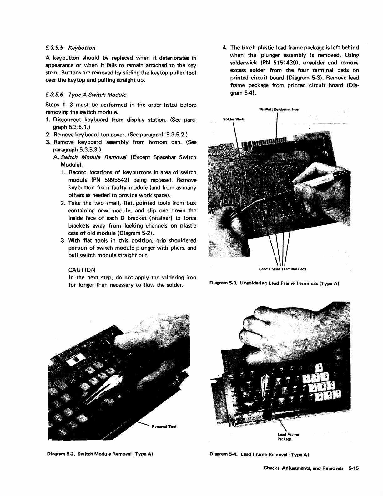
5.3.5.5 Keybutton
A keybutton should
appearance
or
when
stem. Buttons are removed
over the key
top
be
replaced when
it
fails
to
remain attached
by
sliding the key top puller tool
and pulling straight up.
it
deteriorates in
5.3.5.6 Type A Switch Module
Steps
1-3
must be performed in the order listed before
removing the switch module.
1.
Disconnect keyboard from display station.
graph 5.3.5.1.)
2.
Remove keyboard
top
cover.
(See
paragraph 5.3.5.2.)
3. Remove keyboard assembly from bottom
paragraph 5.3.5.3.)
Switch Module Removal (Except Spacebar Switch
A.
Module):
1.
Record locations
module
(PN
keybutton
as
others
2. Take the
needed
two
containing new module,
inside face
brackets away from locking channels on plastic
case
of
old module (Diagram 5-2).
3. With
flat
portion
tools in this position, grip shouldered
of
pull switch module straight out.
of
keybuttons in
area
5995542) being replaced. Remove
from
faulty
module (and from
to
provide
work
space).
small, flat, pointed tools
and
slip one down the
of
each
D bracket (retainer)
switch module plunger
with
to
the key
(See
para-
pan.
(See
of
switch
as
many
from
box
to
force
pliers, and
4. The black plastic lead frame package
when
the
plunger assembly
is
removed. Usinp
solderwick (PN 5151439), unsolder and
excess
printed
frame package from printed
solder from the fou r terminal
circuit
board (Diagram 5-3). Remove lead
circuit
gram 5-4).
15-Watt Soldering Iron
is
left
behind
remOVE
pads
board (Dia-
on
CAUTION
In the next step, do
for
longer than
necessary
not
apply the soldering iron
to
flo·"" the solder.
Lead Frame Terminal Pads
Diagram 5-3. U nsoldering Lead Frame
lead
Frame
Package
Terminals
(Type
A)
Diagram 5-2.
Switch
Module
Removal
(Type
A)
Diagram 5-4. Lead Frame Removal
Checks,
Adjustments,
(Type
A)
and Removals
5-15
Page 74

Note:
distorted during
it back
squeezing
seat firmly against the sides of
If
the
switch mounting frame becomes
removal
to
its normal position. This can
the
0 brackets together until they will
of
the
old module, form
the
be
done by
new module
housing.
B.
Switch Module Replacement:
Do
not
disassemble
replacement module. Lead frame and plunger
assemblies
follows:
as
1.
Check
boss on bottom
(Diagram 5-5). If it
that
boss. Compress and rotate spring until
expands around boss.
should be parallel
Note:
check the
not bent and
of
are matched during manufacture. Proceed
that
return spring
of
is
firmly seated on spring
plunger
is
of
new switch module
not, invert switch module so
lead frame terminals are up. Place spring on
last coil
When
properly seated, spring
to
long axis
When
the plunger return spring
lead frame terminals
that
they are parallel
of
switch module.
is
to
see
that
to
the long axis
in
they are
the switch module.
place,
2.
Insert module into keyboard switch mounting
frame, with orientation arrow on top of
pointed
modules (Diagram 5-6).
sure
bottom
terminals extend through
in
the same direction
As
as
module
plunger return spring seats on raised boss on
of
mounting frame and
holes
in
board.
Diagram 5-6. Switch Module Orientation (Type A)
module
arrows on other
is
inserted, be
that
the four
printed-circuit
Lead Frame
Terminals
Diagram
5·5.
,/
I(
I I
Switch Plunger
I~Spring
I
I
) Plunger
Return
Spring
Boss
Return
Spring POSitioning (Type
A)
Once new module
is
in
place, check for
the
following conditions:
• Plunger moves freely.
•
Top surface of module
modules.
other
• 0
brackets on mounting frame lock module
firmly
in
place.
Note: Should
module
careful not
it
be necessary
to
correct any of these conditions,
to
mar any portion
is
even with those of
to
remove the new
of
the plunger,
be
since operation of the module and/or retention
of the keybutton
would be affected.
CAUTION
In
the
next step, do not apply soldering iron for
longer than necessary
3.
Solder terminals
amount
of
solder.
of
to
flow the solder.
lead frame.
Use
a minimum
4. Reassemble key buttons on switch modules. Check
to
see
that
correct keybuttons are returned
to
correct module positions.
Install the assembly on the bottom pan, replace
5.
keyboard
top
cover, and reconnect keyboard
to
display station.
5-16
Page 75

5.3.5.7 Type A Spacebar Assemblies
Type A spacebar assemblies consist
(PN
5995544) and the spacebar switch module (identical
other
switch modules). The spacebar group comprises
spacebar,
modules. Replacement
removal
removals
the
torsion bar, and
of
any spacebar part requires
of
the spacebar and torsion bar. Perform the
in
paragraphs 5.3.5.1 through 5.3.5.3 for access
of
the
spacebar group
the
two spacebar guide
the keyboard assembly.
A.
Spacebar Removal:
1.
Grasp torsion bar near one end with thumb and
forefinger (Diagram 5-7) and flex it upward, snapping
it forward
out
of
retaining lugs on spacebar guide
module.
2. Swing loose end of torsion bar upward, and disengage
it from other spacebar guide module.
3.
Lift
spacebar straight up
out
of
spacebar guide
modules. This exposes spacebar guide modules and
spacebar switch
module.
to
the
to
5.
If spacebar switch module
switch
module as described
is
to
be replaced, remove
in
paragraph 5.3.5.6A,
steps 2 through 4.
B.
Spacebar Replacement:
1.
If spacebar switch module
procedure described
in
is
to
be
replaced, use
paragraph 5.3.5.68, steps 1
through 3.
If spacebar group
2.
is
to be replaced, insert new
spacebar guide modules into mounting frame;
careful
to
modules firmly
Insert spacebar guides
3.
drop spacebar
4.
Holding torsion bar
insert end
the
to
have torsion bar retaining lugs positioned
front.
Be
in
in
place.
of
torsion bar
sure
that
D brackets lock
place.
in
spacebar guide modules, and
at
a suitable angle and position,
in
the hole
in
one spacebar
guide (Diagram 5-8). At the same time, engage torsion
bar with retaining
torsion bar
to
lugs
on guide module. Lower
horizontal. Flex it as during removal,
and insert other end simultaneously into hole
spacebar guide and into retaining lugs on other guide
module.
5. Operate spacebar
freely and
to
see
that
switch module operates
that
torsion bar and spacebar guides
bind.
6.
Replace keyboard
to
display station.
top
cover and reconnect keyboard
in
do
be
gu
ide
other
not
Diagram 5-7. Torsion Bar Removal
4. If spacebar group
guide modules
as
step 2. (See Diagram 5-8).
(Type
is
to
be
explained
A)
replaced, remove spacebar
in
paragraph 5.3.5.6A,
Lift
module straight
with thumb and forefinger.
8ernoval
Toot
Diagram 5-8. Spacebar Guide Module Removal
(Type
A)
out
5.3.5.8 Keybutton Support Modules - Type A Keyboards
Only
The longer keybuttons, 1-3/4 and 2-3/4 units long,
A keyboard
utilize support modules
PN
5995543 and
·on
Type
PN
5995547, respectively.
A.
Support Module Removal:
1.
Remove keybutton(s)
to
provide adequate work
space.
2.
Take the two small, flat, pointed tools from box
containing new
of
each D bracket (retainer)
from
locking channels on plastic case
With
3.
flat tools
portion
module, and slip one down inside face
to
force brackets away
of
old module.
in
this position, grip shouldered
of
support module plunger with pliers, and
pull old module straight out.
B.Support
1.
Module Replacement:
Check
that
return spring
boss on bottom
it
is
not, invert module, place spring on boss, and
of
plunger of
is
firmly seated on spring
nfi!W
support module. If
compress and rotate spring until last coil expands
around boss.
2.
Insert new module into keyboard switch mounting
top
of
frame, with orientation arrow on
housing pointed
modules.
As
in
same direction as arrows on other
module
is
inserted, be sure plunger
module
Checks, Adjustments,
and
Removals 5-17
Page 76

return spring seats on raised boss on bottom
of
mounting frame.
Once new module
moves freely,
extend above other modules, and
mounting frame have locked module firmly
3. Reassemble key buttons
that
correct keybuttons are returned
that
is
top
in
su
on
place, check
rface of modu
that
Ie
that
D brackets on
plunger
does not
in
switch modules. Check
to
correct
place.
module positions.
5.3.5.9 Type B Module
Steps
1-3
must
be
performed
removing the module.
working
module flyplate and the
problem. Before keyboard disassembly, prepare a smooth,
on
the keyboard.
printed
in
Cleanliness
Any
particle between the key
circuit
the order listed before
is
important when
board
is
a potential
clean work area by wiping contamination away with a
lint-free cloth dampened with isopropyl alcohol. Gently
tap, brush, and shake the keyboard assembly
most loose particles
that
could get into the
to
PC
board and
remove
flyplate area during disassembly and reassembly.
1.
Disconnect keyboard from display station. (See para·
graph 5.3.5.1.)
2. Remove keyboard
top
cover. (See paragraph 5.3.5.2.)
3. Remove keyboard assembly from bottom pan. (See
paragraph 5.3.5.3.)
A.
Module Removal (Including Spacebar Module):
Diagram 5-9. Screw Loosening
6.
Lift
the all-keys assembly from the circuit board,
and place
up)
the
assembly right side up (keybuttons
in
the
clean area. Handle the all·keys assembly
by the sides (Diagram
depress any keys while removing assembly, since a
flyplate could detach.
(Type
B)
5-10).
Be
careful not
to
Note: See paragraph 5.3.5.10 for spacebar removal if
spacebar module
1. Ensure
inate
the
is
to
be replaced.
that
all
small particles
that
might contam-
keyboard assembly are removed from the
work area.
2. Record locations of keybuttons
that
is
being replaced. Remove key button from
faulty module and from as many others as may
required
to
provide enough work space. '
3. Place keyboard assembly upside down
in
area
of
module
in
be
the
cleaned area, and loosen the screws holding base
plate and circuit board
(Diagram
5·9).
Do
to
the all-keys assembly
not
remove the holding screws
at this time.
to
slide
expose
4. Place keyboard assembly right side up, and
one corner off
the
work surface edge
one holding screw. With fingers, remove hblding
screw from bottom.
5. Carefully rotate keyboard assembly and remove
remaining holding screws, one
all-keys assembly and
PC
at
a time. Keep the
board together.
Circuit Board and Electronics Assembly
Diagram
5·10.
Keyboard
Note: Replace
comes off.
Do
Assembly Separation
the
key module
not
attempt
to
(Type
repair the module.
Repaired modules can cause intermittent failures.
B)
if
the flyplate
5-18
Page 77

7. Raise
8.
the
module
key
down on
out
snaps
edge of
the
of
the
all-keys assembly nearest the
to
be replaced
shoulder
the
retaining plate (Diagram 5-11).
about
of
the
key module until it
Select either removal method, a
is
most conven ient.
a.
Lift
the
all-keys assembly, leaving behind the
defective key module.
assembly
b.
Lift
defective
rightside up
the
all-keys assembly, leaving behind the
module. Place the all-keys assembly
upside down, either
Place the all-keys
in
the
on
the existing system
or
clean area.
keyboard mounting hardware and brackets or
on prepared supports (such
or
standoffs).
B.
Module Replacement:
1.
Observe orientation
Ensure
that
in
the
same position as
in
the
all-keys assembly.
Install new module
2.
the
all-keys assembly over
Sa
step
the
key module
the
from
the
alignment
(PN
was used for removal)
in
the
bottom (if step
as
blocks of wood
of
the
new key module.
lug
and keystem are
the
rest of the modules
1772948) by lowering
the
new module (if
retaining plate by hand
8b
removal).
Clean the printed circuit board (Diagram 5-12)
3.
and key module
flyplates by carefully wiping
each with a lint-free cloth dampened with
isopropyl
remove flyplates from key modules.
4. Align
plate,
alcohol.
the
PC
board, insulator, and
8e
careful
not
holding screw holes through base
top
present). Diagram 7-18 shows the correct
locations
of
these components. Lower the
all-keys assembly into place.
5. Carefully slide one corner of the keyboard
assembly off
the
work area edge, and install
one holding screw finger tight. Rotate keyboard assembly carefully, and install remaining
screws finger tight.
6. Turn keyboard assembly upside down, and
all
tighten
7.
Turn keyboard assembly rightside up, and
reinstall keybuttons
holding screws with a screwdriver.
in
proper locations.
8. Manually check operation of each key module.
9. With an ohmmeter, check for continuity
between
pin
008.
the
base plate and
The
two
KB
base plate grounding studs
(Diagram 5-13) must contact the
ground circuit.
10. Install
the
keyboard assembly on the bottom
pa
n,
replace keyboard
reconnect keyboard
top
to
the display station.
1/4
inch. Press
b,
below,
or
by snapping
was used for
to dislodge
insulator (if
1 connector
PC
board
cover, and
that
or
Diagram
5-11.
Module
Removal
Circuit
Diagram 5-12.
Diagram 5-13. Base Plate G rou
Board and
(Type
B)
Electronics
nd
Studs
(Type
Assembly
Ground
B)
(Type
Stud
B)
(2)
Checks,
Adjustments,
and Removals
5-19
Page 78

5.3.5. 10 Type 8 Spacebar
Perform the removals described
through 5.3.5.3 for access
A. Spacebar Removal:
1.
Grasp spacebar button
of
the
modules) and remove by applying even upward
force.
2.
Pivots can be removed
the tip
the side
of
a screwdriver placed
of
the
to
the
keyboard assembly.
at
each extreme end (outboard
(if
pivot (Diagram 5-14).
in
paragraphs 5.3.5.1
required) by prying with
in
the
molded slot
in
1.
Clean
the
work area and prepare the keyboard.
steps
1-3
of paragraph 5.3.5.9.)
2. Disassemble keyboard.
5.3.5.9A.)
3. Reassemble keyboard.
5.3.5.9B.)
5.3.6 Audible Alarm (Optional Feature)
The audible alarm device circuitry
metal box mounted on
inside the front cover. The audible alarm box
vertically
Model 2 display stations.
1.
2.
3. Remove circuit board from
4. Remove cable wires from audible alarm circuit board
with long-nosed pliers
5. Replace
color code
on
Model 1 display stations and horizontally on
Remove front cover.
Remove audible alarm box from chassis. Box can be
removed from snap fasteners by rocking metal box while
pulling away from chassis.
in
reverse order. Circuit board
of
wires
(Use
steps
(Use
steps
is
the
base chassis beneath
the
metal box.
or
small blade screwdriver.
to
be replaced.
3-6
of
2-9
of
packaged
is
etched with
(Use
paragraph
paragraph
in
a small
the
CRT,
is
mounted
I Diagram
B.
5.3.5.11 Circuit Board and Electronics Assembly - Type B
The circuit board and electronics assembly
replaceable unit on Type B keyboards. To remove or
replace
as
5·14.
Spacebar
Spacebar Replacement:
1.
Snap any pivots removed
mounting frame.
2.
Place spacebar button over its respective modules,
and lower it into position while engaging the
stabilizer bar
3. Apply downward pressure on spacebar
directly over spacebar modules to seat
button.
4. Check spacebar operation for binds.
present,
right module stem. This stem can be straightened
eliminate the bind.
5. Replace keyboard
to
display station.
Keyboards Only
the
circuit board and electronics assembly, proceed
follows:
Pivot Removal (Type B)
in
the
two pivots.
the
most common problem
top
cover, and reconnect keyboard
in
step 2 (above) into
at
the points
the
If binds are
is
a slightly bent
is
spacebar
a field-
5.3.7 Security Keylock
5.3.7. 1 Model 1
1.
Remove screws that hold keylock assembly
2.
Release cable clamps
logic board.
3. Remove cable leads from connector
Note positions from which wires are removed (for later
reconnection) .
4.
Lift
switch cable assembly free
5.
Reassemble in reverse order.
removed
positions and
in right side cover.
to
5.3.7.2
1.
Remove screws
2.
Remove keylock assembly cover.
3. Remove cable leads from switch with pliers
screwdriver. Note terminals from which leads are
removed (for later connection).
4. Remove cable strain relief from hole
5. Remove cable from keylock assembly.
6. Reassemble
assembly with hole
in
Model2
in
step 3 are replaced
that
(Optional Feature)
that
route switch assembly cable
of
keylock assembly
that
hold keylock assembly
reverse order. Make sure
in
right side cover.
to
at
socket A 1 Z3.
machine.
Make
sure
in
proper connector
is
aligned with hole
to
in
switch assembly.
to
align keylock
frame.
that
frame.
or
to
leads
small
5-20
Page 79

5.3.8
Selector Ught-Pen (Optional Feature)
5.3.8.1 Model1
from
base
of
1. Remove screws
remove cable.
2.
Unplug feature cable from logic board cable
3. Unscrew nylon
center
rear
4. Remove screw
and
ground wire
5. Slip cable
of
out
cable
board
and
to
of
slotted
clamp
assembly.
retainer
rear
selector light pen holder;
screw
that
that
clamps routing cable
of
chassis.
hole
at
center
6. Replace in reverse order. Make sure
reconnected
so
slot
7. Position light-pen cable
from holder
to
chassis, and
that
extra insulation
to
cable
end
that
on
in
pen holder
of
pen is
,cable is positioned in
cable
about
holds cable
rear
of
that
ground wire
acts
as a grommet.
so
that
30
socket
chassis.
distance
inches.
Y 4.
to
not
aids are
CEMs,
5A.1
Ceaning
The importance
keyboards
the
key module flyplate and
potential problem.
5.4.1. 1 Work
Before beginning any keyboard disassembly, prepare a
is
smooth,
with a lint-free cloth dampened with isopropyl
Gently
remove most loose particles
and flyplate area during disassembly and reassembly.
intended
or
other
published
cannot
A,.
clean work area
tap,
brush,
to
replace
data.
of
cleanliness when servicing
be overemphasized.
and
shake
by
that
the
existing procedures,
Any
the
printed
wiping
contamination
the
keyboard assembly
can
get
particle between
circuit board
into
the
Type
away
alcohol.
PC
board
B
is
a
to
5.3.8.2 Model 2
1.
Remove screws from base
remove cable.
2. Unplug feature cable from logic board cable
3. Release cable from cable clamps
bottom
of
chassis.
of
selector light pen holder;
socket
that
route
cable
Y
4. Disconnect ground wire from frame.
5.
Slip cable
chassis.
Replace in reverse order. Make sure cable
6.
cable clamps so
grommet
Make sure
7. Position light pen
from holder
inches.
5.3.9
1. Disconnect card reader cable ground strap from chassis.
2. Remove card reader cable
Model 1 display stations, nylon cable clamp
removed. On Model 2 display stations,
retainer
3. Replace in reverse order.
4. Ensure
sockets
ground terminal.
out
of
slotted hole
that
extra
where cable passes through hole in chassis.
that
ground
to
Operator Identification Card Reader (Optional
Feature)
must
be
that
all
and
that
wire
cable
cable
end
unhooked
I/O cable
all grou nd straps are attached
at
bottom,
is
insulation
is
reconnected
in pen holder so
of
pen
connector
to
release cable connector.
connectors
on
cable acts as a
to
is
approximately
from its socket.
the
are firmly seated in
right, rear
positioned
frame.
that
distance
must
110
cable
to
chassis
30
On
5.4.1.2 Keyboard Assembly
Before reassembling
circuit board and key module flyplates
4.
cleaned by wiping each with a lint-free
to
with isopropyl alcohol.
remove flyplates from key modules while cleaning. Replace,
rather than
flyplate separates from
of
5.4.2
in
Some minor liquid
sugar, can be removed by first
affected
mixture
water-dampened, lint-free cloth. Finally, clean with lint-free
cloth dampened with isopropyl
Note: Sticky key modules
spill may necessitate replacement
assembly.
5.4.3
be
Two
types
module and a new
currently
modules
to
3277
mittent
attempt
Uquid
Spills
fly plates with a lint-free
of
water and mild hand soap.
Key Modules
of
in
use
must
display stations. These modules can cause inter-
errors.
the
keyboard assembly,
Be
to
repair,
the
spills, such as
must
key modules,
"super
on
Type
not
be used
must
cloth
careful
module.
"washing"
alcono!.
slick"
B keyboards.
on
keyboards
not
to
the
key
module if
soft
drinks
or
the
cloth
dampened with a
"Rinse"
be replaced. A severe liquid
of
the
entire
the
original "black
white
body
Super
that
the
printed
be
carefully
dampened
dislodge
coffee with
PC board and
module, are
are attached
or
the
with a
keyboard
body"
slick key
5.4 TYPE B
The
Symptom
Diagrams
tions.
in
this
keyboard faults. This section provides miscellaneous main-
tenance aids
KEYBOARD
Index
in
Chapter 4 isolate
The
check
chapter
to
MAINTENANCE AIDS
in
Chapter 3
and
removal procedures presented earl ier
provide detailed instructions
supplement
and
the
Troubleshooting
Type
B keyboard malfunc-
the
existing procedures. These
for
repairing
5.4.4 Contamination Shields
Some keyboards have foam
a 1.S-mil protective membrane/shield
contamination from entering
during customer use. The presence
of
the
function
shown
in
Diagram 7-18.
EC level
strips, foam side insulators, and
the
PC
board
of
of
the
keyboard.
Checks. Adjustments, and Removals 5-21
added
to
prevent
and
flyplate area
these shields
The
shields are
is
a
Page 80

5.4.5 Protective Membrane/Shield
When removing a key
protective
shield, care must be taken
shield when snapping
module from a keyboard with the
out
the defective module.
5.4.6 Ground Check
There
should
grounding studs (Diagram 5-13) and
on
the
ohmmeter connected between the
ground pin,
be
continuity between the two base plate
PC
board. Grounding can
008,
at
the
interface signal connector,
the
be
base
5.4.7 Ground Loop Isolation
Nonconductive inserts have been added
holding
base plate and
assembly. With
the 3277, check
assembly
screws on some keyboard assemblies
PC
board
dc
ground from
the
keyboard assembly disconnected from
to
ensure
that
the
base plate and all-keys
are
not
electrically shorted.
not
to
puncture
dc ground circuit
checked with an
plate and
KB
to
the base plate
to
isolate
the
all-keys
the
the
1.
the
5.4.8 Crooked
Key
module stems can
crooked
to
tighten loose key tops.
or
looking key top. The keystem ears can be widened
Loose
Key
tops
be
formed left
or
right
to
align a
5-22
Page 81

Section 6. Reference Data
This section contains miscellaneous reference information
that
can
be
helpful in maintaining
IBM
3277 Display
Stations.
CONTROLS
6.1
Controls are divided into two categories: external and
internal. External controls are those
without remov
ing
covers. I nternal controls are those
are under covers and are accessible
nel
only. The audible alarm volume control, although
located under
control because
the
front cover,
the
display station operator can adjust
that
are accessible
to
maintenance person-
is
considered an external
that
the
volume.
6.1.1 External Controls (Diagram
6.1.1.1 OFF-PUSH (Power, Brightness, and Contrast)
The OFF-PUSH switch
adjusts
the
display image brightneS5 and contrast. I t also
is
controls display station power. Pulling
CRT
Bezel
6-1
)
a triple-function control
the
switch
Indicators
that
out
(3)
toward
overall displayed image
Brightness control (outer knob) clockwise;
made dimmer by rotating
Contrast control (inner knob)
the
clockwise reduces
and normal intensity characters; rotating
counterclockwise increases
6.1.1.2 Security Keylock (Optional Feature)
This operator control
key must
position)
key must remain
station enabled.
unless it is returned
6.1.1.3 Selector Light-Pen Tip Switch (Optional Feature)
the
operator turns display station power on. The
is
made brighter by rotating
the
knob counterclockwise.
is
on a concentric shaft with
Brightness control. Rotating
the
difference in contrast between high
the
is
a key-operated switch lock. The
be inserted
to
enable
the
in
the
The
key cannot
to
in
the
lock and turned
display station for operation. The
On position
the
Off
the
difference
be
removed from
position.
Contrast control
in
to
keep
the
image
the
contrast.
on
(horizontal
the
the
the
The
control
display
lock
The selector light-pen contains a spring-loaded switch in its
tip. The switch
is
used
to
select detectable fields
on
the
is
OFF·PUSH
OFF-PUSH Switch
(Power/Contrast/Brightness)
Diagram 6-1. External Controls
and
IBM
CRT
Indicators
SYSTEM
AVAILABLE
INSERT
MODE
INPUT
INHIBITED
Security Key
Reference Datil 6-1
Page 82
screen by placing
field and pushing
Removing
the
the
point
the
barrel
tip from
the
of
of
screen
the
pen
the
pen toward
on
turns
the
the
desired
the
switch
automatically.
6.1.1.4 Audible Alarm Volume (Optional Feature)
The loudness
display station operator by turning
volume control.
to
the
protrudes downward from
right side
the
control protrudes frontward from
box
on
6.
1.1.5 Keyboard Audible
A knob
the volume
Volume can
depressed)
6.1.2
of
the
audible
tone
can be adjusted by
the
The
front
cover must be lowered for access
control. On Model 1 display stations,
the
audible alarm box
of
the
base chassis. On Model 2 display stations
the
the
left side
at
the
to
of
the
upper chassis.
Response
rear of
of
be
adjusted from
the
keyboard
the
keyboard audible response device.
bottom
off
(no click when a key
maximum loudness by rotating
Internal Controls
audible alarm
the
audible alarm
plate adjusts
the
knob.
data
screen.
off
the
control
on
the
is
spacing between character rows and, thus, determines
overall height
control
6.1.2.6
This control
located
reference line
image adjustments are made.
reference line remains stationary during
is
TOP
on
not
of
the
displayed image. The
used
in
Model 1 display stations.
MARGIN
is
a screwdriver-adjustable potentiometer
the
analog card.
on
the
CRT, from which all
The
Once
ROW
control sets
other
the
control
other
SPACING
the
vertical
is
set,
vertical
character and image adjustments.
6.1.2.7 Image
The deflection yoke, mounted
tilt
the
the
image for squareness with
6.1.2.8 Magnetic Centering Rings
The magnetic centering rings are mounted
neck, directly behind
rings are rotated
geometric center
Tilt
on
the
CRT neck, is used
entire displayed image. Rotating
the
edges
the
deflection yoke.
to
position the displayed image
of
the
CRT.
the
of
yoke
the
CRT bezel.
on
The
adjusts
the
centering
about
the
top
the
to
CRT
the
6.1.2.1
This momentary-contact switch
INTEN
CRT
is
located
on
the
display
station analog card. The switch overrides intensity and
blanking
complete raster
6.
1.2.2 Focus
This control
located
the sharpness
pulses generated by control logic and causes a
of
on
scan lines
is
a screwdriver-adjustable potentiometer
the
HV
power supply. Turning
of
the
dots
to
be displayed when pressed.
the
control varies
that
form
the
characters on
the
screen.
6.1.2.3 WIDTH
The WIDTH control
tiometer located
the
varies
total width
6.1.2.4 CHAR
This control
located
vertical
horizontal dot-to-dot spacing, which alters
of
the
HEIGHT
is
on
the
dot-toodot spacing
Model 1 display station, it determines
the
displayed image.
6.1.2.5 ROW SPACING (Model 2 Display Stations Only)
This control
located
on
is
the
is
a screwdriver-adjustable poten-
on
the
analog card. Turning this control
displayed image.
a screwdriver-adjustable potentiometer
analog card. Turning
of
the
the
control varies
displayed image. On
the
overall height
a screwdriver-adjustable potentiometer
analog card. Turning
the
control varies
the
the
of
6.1.29
This control
located on
the
6.2
Display
categories: external and
those
covers.
removed.
-12V Supply
is
a screwdriver-adjustable potentiometer
the
voltage
-12V regulator card. Turning
output
of
the
-12V power supply.
the
INDICATORS
indicators, like controls, are divided into two
internal. External indicators are
that
can be seen
To
observe internal indicators, covers must be
without
removing any machine
Internal indicators are accessible only
maintenance personnel.
6.2.1 External Indicators (Diagram 6-1)
The three external indicators on
displayed as
small boxes (blips) generated by analog
circuitry. They are displayed
at
3277
Display Stations are
the
right edge
Each indicator has its function identified by a
CRT bezel, adjacent
indicators
6.2.1.1 SYSTEM A
is
controlled by
This indicator
display stations and
stations.
signifies
control
In remote system configurations,
that
unit
(TCU)
is
displayed
the
carrier
to
the
indicator. The brightness of
the
Brightness control.
VAILABLE
at
character row
is
online when lighted.
Indicator
at
character row 4
is
on
and
lOon
Model 2 display
that
the
In
control sets
of
the
CRT.
label
on
on
Model 1
the
indicator
transmission
local system
to
the
the
6-2
Page 83

configurations,
channel 'operational
6.2.1.2
INSERT
This indicator
display stations and
stations.
the
on
station
keyboard
is
remains on, and
until
the
6.2.1.3
INPUT
This indicator
display stations and
stations. The
the
display station from
Operator Identification Card Reader
and
indicator
the
RESET key. When
the
indicator being
out'
MODE Indicator
is
displayed
at
character row
The
indicator lights when
is
pressed.
in
the
Insert mode
the
display station remains in Insert mode
RESET key
is
pressed.
INHIBITED
is
displayed
at
character row
tag line
is
active.
at
character row 6
12
the
It
signifies
of
operation.
Indicator
at
character row 8
14
lighted indicator signifies
the
keyboard, selector light pen,
is
extinguished by program control
the
security key lock
on
signifies
on
Model 2 display
INSERT
that
The
on
Model 2 display
that
manual input
is
blocked.
or
that
the
on
Model 1
MODE
key
the
display
indicator
on
Model 1
The
by pressing
is
off, this
to
indicator lights.
Internal Indicator (SWEEP INDIC)
6.2.2
The SWEEP INDIC indicator
is
a neon bulb mounted
on
the display station analog card. The lighted indicator
that
the
signifies
horizontal deflection circuits are oper-
ating.
6.2.3 Arc-Suppression Neon
a~c-suppression
The
board
in
Model 1 display stations and on
distribution board
indicator and will never be seen lighted. The
the
neon bu
of
and
the
display station frame ground. The neon acts
momentary short circuit whenever
neon
is
located
in
Model 2 display stations. It
Ib
are connected between de ground
on
the
the
difference
arc-suppression
the
two
voltage
is
not
an
elements
(R
ET)
as
in
potential between its two elements would have exceeded approx.imately 90V. The difference
the
generated by
to
tube
arc. Arcing causes transients
inherent characteristic of a cathode-ray
the tube. Restricting potentials
in
potential
to
in
the return path
90V
to
ground protects
is
occasionally
of
display station circuitry from possible damage.
KEYBOARDS (Optional Feature)
6.3
Four keyboards are used with
Keyboards
of
the
same type are interchangeable among
321"1
Display Stations.
display stations having keyboard adapter circuitry installed.
EBCDIC
is
the basic code used
on
all keyboards.
6.3.1 Types
6.3.1. 1 Typewriter Keyboard
of
Keyboards
The typewriter keyboard uses a standard typewriter key
of
66
layout
be
may
Diagram 6-2 illustrates
6.3.1.2 Operator Console Keyboard
The operator console keyboard uses an
keys. An additional 12 Program Function keys
incorporated
in
the
standard typewriter keyboard.
the
typewriter keyboard.
IBM
1052-7
key layout with an additional 12 Program Function keys.
the
Diagram 6-3 illustrates
6.3.1.3 Data
The two data
Entry
entry
alphameric keys and
trates the two data
EBCDIC Keyboard Codes
6.3.2
The
EBCDIC
entry
code
operator console keyboard.
Keyboards
keyboards use
30
control keys. Diagram 6-4 illus-
66
keys, consisting
keyboards.
is
the standard code used with
system keyboards. Diagram 6·5, sheet 1, shows the keyboard codes for the typewriter and operator console
keyboards.
Graphics column
Characters (and functions) are shown
as
they appear on typewriter keyboard
key tops. The operator console keyboard key layout
similar. Sheet 2 shows the EBCDIC code arrangement used
on the data entry keyboard(s). Diagrams 6-6 and 6-7 show
ASCI
I and
WTC
the codes for unique
6.4
ASCII OPTIONS
ASCII*
character generator and keyboard options may be
present on
available only
a
3277
Display Stations. ASCII options are
in
the United States and Canada. The
language characters.
following paragraphs describe the characteristics of these
options.
6.4.1
ASCII Character Generators (Optional Features)
Two
ASCII
character generator options allow
code set
symbols [,
EBCDIC code set. ASCII option A uses
-',
to
be displayed.
],
\ , and
The
ASCII code set includes
"which
are
while option B substitutes
not
used
in
the
symbols I and
the
symbols ! and 1\
respectively. Each option requires a different character
-ASCII
American
change, X3.4-1968.
National
Standard Code
for
Information
type
of
all
3270
in
the
ASCII
the 3277
Inter-
36
the
is
the
Reference Data
6·3
Page 84
generator
display
option;
same
6.4.2
Two
3277
writer
unique
keys
keyboards
tionally
but
installed
Option
symbols
provides
logic card in
station
is
not
however, if logic
type
number
ASCII Keyboards (Optional Features)
ASCII
typewriter
Display
Station.
keyboards
ASC
II
characters
1-12
are included
location
affected
card
must
keyboards
Tt-ey
described
are
card
in
are serviced like EBCDIC keyboards,
they
are
the
same. Unique logic
ASC
II
character
to
enter
A provides
I (logical or)
the
64
and
the
ASCII
generator
display
64
ASCII
and
character
(exclamation point) for logical
logical
not.
K2. Maintenance
by
the
presence
K2
must
be changed,
be
used.
can
be
attached
are
similar
in
paragraph
included
the
to
EBCDIC type-
6.3.1.1,
on
some
78-key version. ASCII
cards
option A or B must
the
unique
character
-,
(logical
or
ASCII characters.
set
not).
set
but
and 1\ (circumflex)
of
of
the
ASCII
to
except
key
tops.
and
opera-
are
not
used,
including
Option
substitutes
the
the
the
PF
be
the
B
for
6.5 REFERENCE
Diagrams
6· 7 through
be helpful
Display
foldout
station
page located
6-8 lists all logic cards used
describes
used as
the
probe
(Section 4) are listed
in
maintaining
data
function
points
DIAGRAMS
6-14
contain
flow
is
at
the
of
each card.
in
the
in
Diagram 6-9. ALD references are
reference
IBM
3277
shown
back
in
of
this manual. Diagram
in
the
display station and
All
troubleshooting
Display Stations.
Diagram
logic
data
card
also listed. Logic board jumpering data for the various
keyboard
Diagram 6-11 shows
feature
options
how
is
included
characters are
in
Diagram 6-10.
encoded
keyboard assembly. Diagrams 6-12 and 6-13 show logic
card plugging for
respectively. Logic board pin identification
the
one-half and two-thirds boards,
data
Diagram 6-14.
!
that
FO-l,
I/O pins
diagrams
in
is
given
can
a
the
in
Page 85
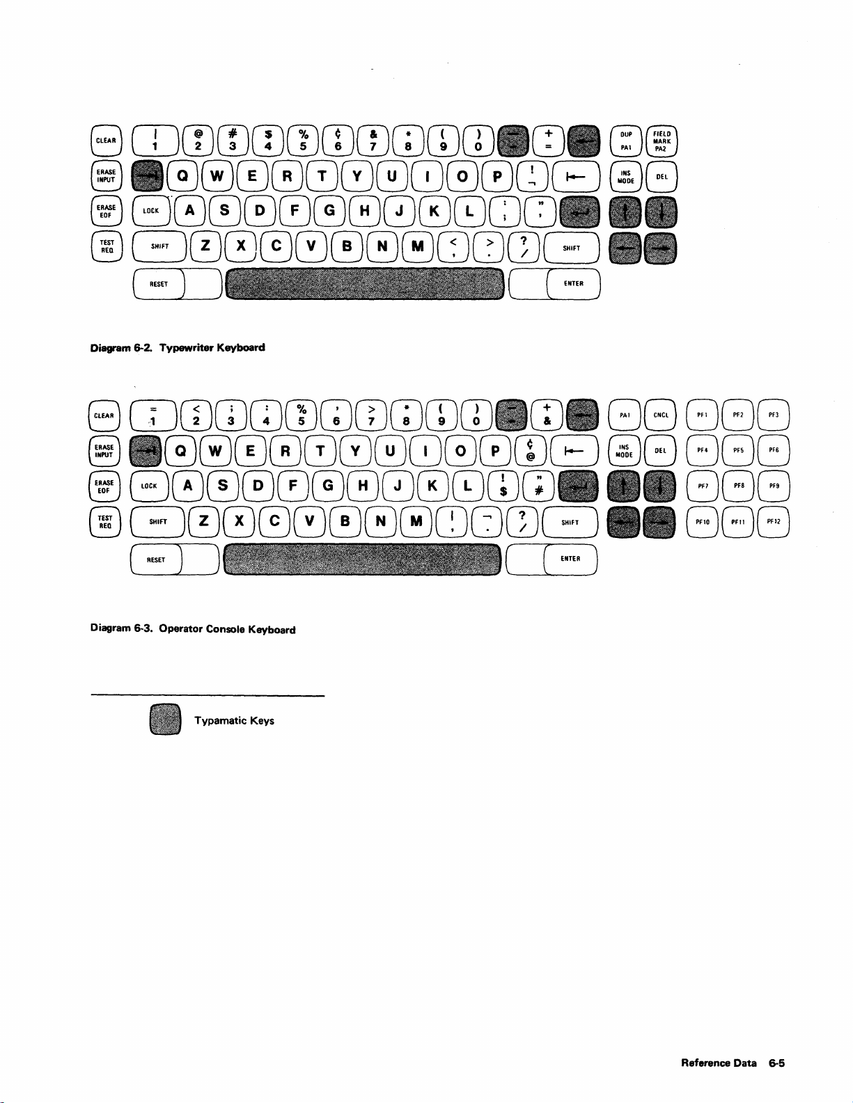
Diagram 6-2. Typewriter Keyboard
8
§)
@
@
CDCDCDCDwCDCDGJGJm
0000080GJG0wB
B000000008GJGJ
G000000GCJCJwG
(
.un
J ) (
Diagram
6·3.
Operator Console Keyboard
Typamatic Keys
CD . 880GO
@8
["',,)
GOG
GGG
8GB
Reference Data
6-5
Page 86

Data Entry Keyboard- Keypunch Layout
8
Q
~
~
~
c:JwGJCDGJ
ERASE
INPUT
r+\ommnmmmmm8r-=-l
lQj~WL!Ul!Jl!J\JUwww
~nl>\(T\mA0\mmm
~WWWWUUl!UWWUJ
r=::-lnm("\f=\mmmmm
L::JWWWWWl!UV!JWLJ
( ) )
Data Entry Keyboard
8
Q
~
~
~
c:JGJGJCDCD
r+\0m"
lQj~
~f<\l>\nmAmmmm
~WWWWUUl!UWWUJ
r=::-l(%"\mn~mmmmmo~
L:::-JwW
neD"
E L!U T
W W W
:~:
GOCIJBGGG
ENTER
~
GG
r::::lG
~
Gt:l
Pf4
U
~
L.::.-J
:~:
GOmGGG GG
f=\mmmmGr-=-l
l!Jl!UWWW
PF4
~
G
PF5
l!UV!VWLJ
. L.::.-J
r::::lG
~
DEL
DEL
(
'BET
J ) (
• Typamatic
Diagram 6-4. Data Entry Keyboards
Keys
[ENTER)
o Numeric Keys
Page 87
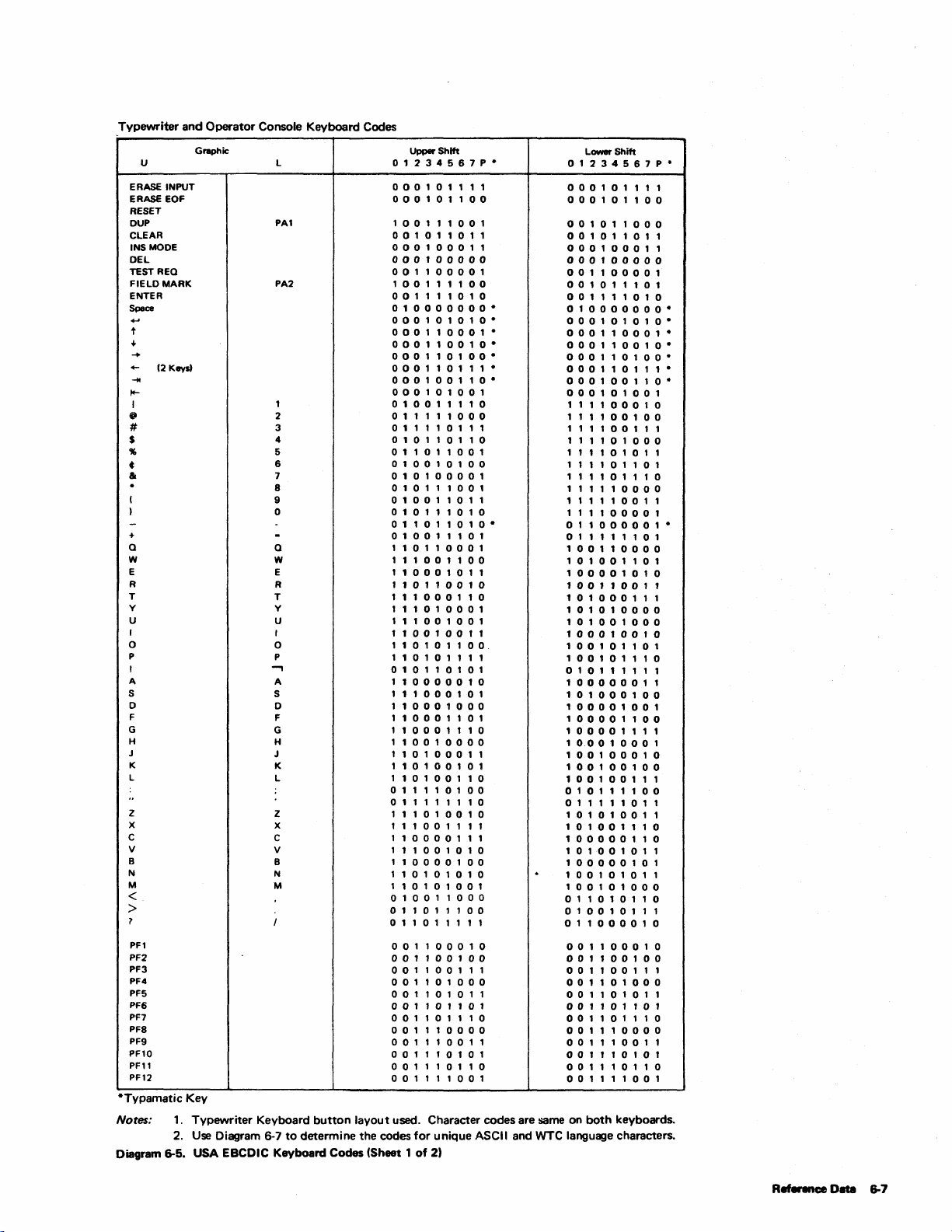
Typewriter
ERASE
ERASE EOF
RESET
DUP
CLEAR
INS MODE
DEL
TEST
FIELD
ENTER
Space
t
.j.
-+
+-
~
14-
I
•
#
$
"
C
&
+
a
w
E
R
T
y
U
I
o
P
I
A
5
o
F
G
H
J
K
L
z
x
c
V
B
N
M
and
INPUT
REa
MARK
(2
Keys)
Graphic
U
<
>
?
PF1
PF2
PF3
PF4
PF5
PF6
PF7
PF8
PF9
PF10
PF11
PF12
*Typamat,c Key
Notes:
Diagram 6-5.
1.
Typewriter Keyboard
2.
Use
USA
Operator Console Keyboard Codes
L
PA1
PA2
1
2
3
4
5
6
7
8
9
o
a
w
E
R
T
y
U
I
o
P
....,
A
S
D
F
G
H
J
K
L
z
x
c
V
B
N
M
button
layout used. Character codes are same on
Diagram 6-7
EBCDIC Keyboard Codes (Sheet 1
to
determine the codes for unique ASCII and
Upper
Shift
o 1
234
5 6 7 P •
000101111
000
1 0 1
100
100
1 1
1 0 1 0 1 0 •
001
101
000
000
000
101
001
101
0 1
001 1 000
100
100
100
101
1 0 1 0 1 1
1 0 1 1 0 1
101
of
2)
100
1
100
101
0 1 •
1 0 •
10·
1 1 1 0
1
000
1 0
0 1
010
0 a 1 0
1 1 1 0
1 0
010
0 1 0
1 0 0
1 1 1
000
1 1 0
0 0
0 1
0
001011011
000100011
000100000
001100001
10011
00111
o 1 0 0 0 0 0 0 0 •
000
000 1 100
000 1 100
000110100·
000"0,,,·
000 1 001
000101001
o 1
01111
011110111
o 1 0 1
011011001
010010100
o 1 0 1
010111001
010011011
o 1 0 1 1 1
011011010·
010011101
110110001
111001100
110001011
110110010
111000110
111010001
111001001
110010011
110101100.
110101111
010110101
1 1
111000101
110001000
110001101
1 1
110010000
110100011
110100101
1
011110100
o 1 1 1 1 1 1 1 0
111010010
1 1 1 0 0 1 1 1 1
110000111
111001010
110000100
1
110101001
o 1
011011100
o 1 1 0 1 1 1 1 1
001
001
001
001
001
001
001
001 1 100
001110011
001 1 101
001110110
001111001
Lower
o 1
000101111
000
1
00101
00101
000100011
000100000
001
001011101
001
o 1 0 0 0 0 0
000
000110001·
000 1 100
000110100·
000 1 101
000 1 001
000
111 1 000
111
111100111
111101000
111101011
111101101
111101110
1
111110011
111100001
011000001·
011111101
100 1 100
10100
1 0 0 0 0 1 0 1 0
100110011
101
101010000
10100
1
100
100 1 011
010111111
1 0 0 0
101
1 a 0 0 0 1
100001100
100001111
1
100 1 000
100 1 001
100100111
010111100
011111011
101010011
1 0 1
1 a 0 0 0 0 1 1 0
101001011
100
100
100
o 1
010010111
011000010
001100010
001
001
001
001
001
001
001
001 1 100
001
001 1 101
001
WTC
language characters.
Shift
234
5 6 7 P •
1 0 1
1
101
100
1 1
101
1 0 1 0 1 0 •
1 0 1
100
111
1 0 0 0 0
1
000
1
000 1 001
1 0 1
000
000
00
0 1 0 0 0 1
001
000
1 0 1
1 0 1
101
0 1 1 0
100
100
101
101
101
101
1 1
000
1 1 0
1 1
100
both
keyboards.
100
000
0 0 1
00·
1 0 •
1 1 •
10·
001
1 0
1 a 0
0 0
101
1 1 1
000
101
1 0
1 1
1 0 0
001
1 0
0 0
1 1 0
1 0 1
011
000
1 0 0
1 1 1
000
011
101
1 1 0
1 1
101
1 0
1
0
0
0
1
R
.....
ce Date 6-7
Page 88
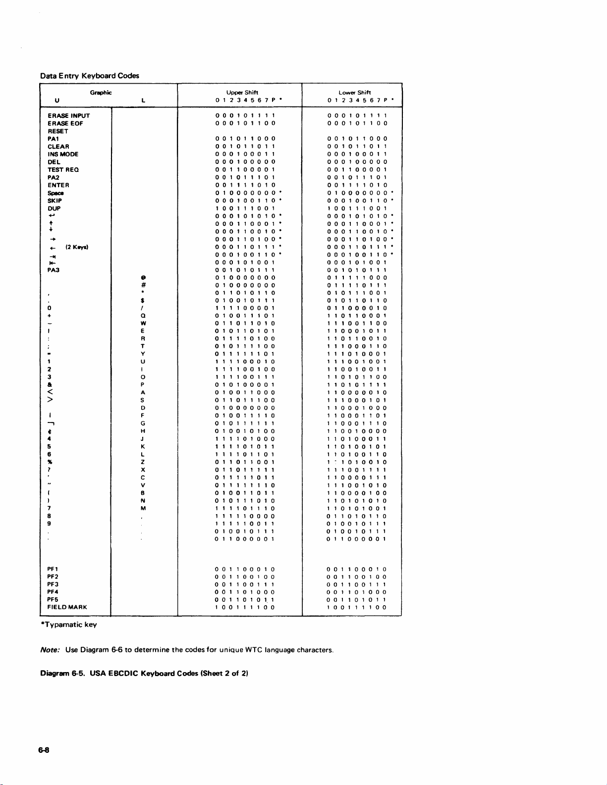
Data
Entry
U
ERASE INPUT
ERASE EOF
RESET
PA1
CLEAR
INS MODE
DEL
TEST REO
PA2
ENTER
Spec:e
SKIP
DUP
t
'"
+-
(2
.....
~
PA3
o
+
1
2
3
a
<
>
....,
~
..
5
6
?
"
(
)
7
8
9
Keyboard
Gl'lIPhic
Keys)
Codes
@II
#
$
I
a
w
E
R
T
y
U
I
o
P
A
S
o
F
G
H
J
K
L
Z
X
C
V
B
N
M
Upper
Shift
o 1
234
L
000
000101100
001011000
o 0 1 0 1 1 0 1 1
000100011
000 1 000
001100001
o 0 1 0 1 1 1 0 1
o 0 1 1 1 1 0 1 0
o 1 0 0 0 0 0
000 1 001
1 0 0 1 1 1 0 0 1
000
000110001·
000 1 100
000110100·
000110111·
000 1 001
000
o 0 1 0 1 0 1 1 1
o 1 0 0
o 1 0 0 0 0 0 0 0
o 1 1 0 1 0 1 1 0
o 1 0 0 1 0 1 1 1
1 1 1 1
o 1 0 0 1 1 1 0 1
o 1 1 0 1 1 0 1 0
o 1 0 1 1 0 1 0 1
o 1 1 1 1 0 1 0 0
o 1 0 1 1 1 1 0 0
o 1 1 1 1 1 1 0 1
1 1 1 1
1 1 1 1 0 0 1 0 0
1 1 1 1
010100001
o 1
o 1 1 0 1 1 1
o 1
o 1 0 0 1 1 1 1 0
o 1 0 1 1 1 1 1 1
o 1
1 1 1 1 0 1
1 1 1 1 0 1 0 1 1
1 1 1 1
o 1 1 0 1 1 0 0 1
o 1 1 0 1 1 1 1 1
o 1 1 1 1 1 0 1 1
o 1 1 1 1 1 1 1 0
o 1
o 1 0 1 1 1 0 1 0
1 1 1 1 0 1 1 1 0
1 1 1 1 1 0 0 0 0
1 1 1 1 1 0 0 1 1
o 1 0 0 1 0 1 1 1
011000001
5 6 7 P •
1 0 1 1 1 1
1 0 1 0 1 0 •
1 0 1
001
000
00
0 0 1
000
00
1 1 1
001 1 000
000
0 0 0 0
001
0 1 0 0
000
0 1 1 0 1
001
1 0 1 1
0 0
00·
10·
1 0 •
10·
0 0
1 0
00
Lower
Shift
o 1
234
5 6 7 P •
000
1 0 1 1 1 1
000
1 0 1
100
00101
o 0 1 0 1 1 0 1 1
000 1 000
000
001100001
o 0 1 0 1 1 1 0 1
o 0 1 1 1 1 0 1 0
o 1
000 1 001
1 0 0 1 1 1 0 0 1
000
000110001·
000 1 100
000 1 101
000110111·
000 1 001
000
o 0 1 0 1 0 1 1 1
o 1 1 1 1 1
o 1 1 1 1 0 1 1 1
o 1 0 1 1 1 0 0 1
o 1 0 1 1 0 1 1 0
o 1 1
1 1 0 1 1
1 1 1
1 1
1 1
1 1 1
1 1 1 0 1
1 1 1
1 1
1 1
1 1 0 1 0 1 1 1 1
1 1
1 1 1
1 1
1 1
1 1
110010000
1 1 0 1
1 1 0 1 0 0 1 0 1
1 1 0 1 0 0 1 1 0
1 1 0 1 0 0 1 0
1 1 1 0 0 1 1 1 1
1 1
1 1 1
110000100
1 1 0 1 0 1 0 1 0
1 1 0 1 0 1 0 0 1
o 1 1 0 1 0 1 1 0
o 1 0 0 1 0 1 1 1
o 1
011000001
1
000
1 1
1 0 0 0 0 0
000
0 0 0 0 •
10·
1 0 1 0 1 0 •
1 0 •
00·
10·
1 0 1
001
000
000
0 1 0
000
00
1 1 0 0
000
1 0 1 1
0 1 1 0 0 1 0
000
1 1 0
000
00
1 0 0 1
0 0 1 0 0 1 1
0 1 0 1 1 0 0
000
001
000
1 0 1
000 1 000
000
1 1 0 1
000
1 1 1 0
000
1 1
000
0 1 1 1
0 0 1 0 1 0
00
1 0 1 1 1
1
1
0
PFl
PF2
PF3
PF4
PF5
FIELD
MARK
*Typamatic
Note: Use Diagram 6-6
key
to
Diagrmn 6-5. USA EBCDIC
determine
Keyboard
the
Codes
codes
(Sheet 2 of
for
001
100
001100100
o 0 1 1 0 0 1 1 1
001101000
o 0 1 1 0 1 0
1 0 0 1 1 1 1 0 0
unique
0 1 0
1,1
WTC
language characters.
2)
001
100
101
0 1 0
000
001100100
o 0 1 1 0 0 1 1 1
001
o 0 1 1 0 1 0 1 1
0 0 1 1 1 1 0 0
1
Page 89

Data
Entry
Language
Key
Graphic
Key
Graphic
Key
Graphic
Key
Graphic
Key
Graphic
Key
Graphic
Keyboard
Codes
USA
EBCDIC
$
$ U
#
# A
@
@
!
!
..
..
4
t
Austrian!
German
U
..
A
0
0
X5A
U
X7F
A
X4A
0
Belgian!
French
$
$
:#
#
@
@
!
I
..
..
4
4
Danish!
Norwegian
l
"-
k
Ii,
(2J
(2J
X5A
Finnish!
Swedish
l
l
A :#
A
0
0
X5A
l l
X7F
k A
X5A X4A
(2J
X7F
b ¢ A
Italian
$
$
:1!
@
@)
!
I
..
..
4
Portuguese
~
Spanish
Pts
~
'0
'0
A
A
X5A
~
X7F
N
N
@ @
@
N
'0 N
X4A
4:
United
Kingdom
f..
Pt
f..
:it
:#
@
I
!
I
!
..
..
$
4
$
Keyboard
Code
01234567P
010110110
011110111
01
11 1 1000
010110101
01
1 1 1 1 1 1 0
010010100
Diagram 6-6. WTC Language
Typewriter
Language
Key
Graphic
Key
Graphic
Key
Graphic
Key
Graphic
Key
Graphic
Key
Graphic,
Key
Graphic
Key
Graphic
Key
Graphic
Keyboard
Codes
USA
EBCDIC
$ $
$
#
:#
@
@
!
I
..
..
•
4
I
I I
-.,
---,
USA USA
ASCII·A
$
:#
:#
@
@
I I
I I
..
..
r
f
I
---,
---,
Keyboard
ASCII-B
$
$
::::
@
(f.u
..
..
I
I
A
A
::
[
f
Codes
(Data
Entry
Austrian!
German
U
(Shift)
U
'j,.
(Shift)
A
o
(Shift)
0
U
U
A
A
0
a
I J
I I
----,
----,
X6A
(None)
Keyboard)
Belgian!
French
$
$
:r
:::
@
@
I
!
. .
..
4:
¢
--,
--,
Danish!
Norwegian
a
(Shift)
a
A:
(Shift)
k
o
(Shift)
0
a
.a
~
~
0
Ql
I I I
I
--,
---,
Finnish!
Swedish
l
(Shift)
l
A
(Shift)
A
o
(Shift)
0
R
a
A
Ii.
0
0
I I
--,
--,
Italian
$
s
:;:
::
(!')
(n)
I
I
..
--
t
t
---,
--,
Portuguese
~
(Shift)
~
'0
(Shift)
0'
A(Sh.tt)
A
~
~
'0
"0
A
A
I
I
--,
---,
United
SPJOISh
Pts
Pt
N
(Shift)
N
to)
,u:
!
1
N o 1 1 1 1 1 1
N
4
4
I
I
----,
---,
Kingdom
f.
£
:;:
=
lll'
(ftl
I
I
.-
S
$
I
I
---,
---,
Keyboard
Code
01234561P
0101
101
0111
101
1 1
01
1 1
o 1
01
10101
010010100
() 1 001
0101
1 1 1 1 1
01
10
10101
1 1 1
10
1 1
U
(j
()
10
()
Diagram
6-7.
ASCII
and
WTC Language
Keyboard
Codes
(Typewriter
Keyboard)
Reference
Data
6-9
Page 90

Location
*A2
Keyboard
*B2
Keyboard
C2
I/O Gating
02
(Modell)
480
Storage
and
Name
Controls
Controls
and
Parity
and
- 2
- 1
Gate
Type
9072
9069
9066
9057
Logic Page
Reference
KMl11-161
,
KM011-071
MG011-061
MB011-061
Function
Major
Tests
characters
protected
Contains
operation
control
or
Units
for
mod ified
and
data.
keyboard
latches, Load.
latches,
Input
Keybd
Reset;
Index; I/O Unlock Decode; MDT Load Bit 7.
Keybd; Allow Char
and MDT latch.
Contains
Tab
KB
controls, Cursor
Controls, and
decoder,
KB
Alpha
Shift;
Insert/Delete
Controls.
Contains
buffer
parity
message
register
check
circuits, late
reg ister,
register,
attribute
and
and
CR
Bits
1-7;
0--9; Load I/O
Load Message Buffer.
gating circuitry
buffer
for line
and
message buffer.
Modell
- Contains
FQ
480-character Serial
message
buffer
Shift
and gates.
Significant I/O Signals
Strobe;
Busy;
1-7,
Strobe.
Keybd
and
P;
NumeriC
CU
Bits
Shift;
KB
Bits0-9;SR
3-11;
KB
Fets
Bits
Out
Bits Bits
Data;
Ser in Bits
Shift
0-9;
Gt;
Fets.
Output
KB
lock; FF Enable; Ld
KB
to
Fets;
Char
KB
Op
Decoder
Char
Edit;
Op
Complete; I nsert Bit
9;
Csr Move; Keybd Bits
Csr
outputs;
Edit;
1-7.
FQ
Ser in Bits
Bfr Bits
2-6;
Fets
Out
0-9;
1-9;
Attb
P Chk Bfr.
Bits
0-9.
Rdy
Mesg
Reg
02
(Model 2)
960
Storage
E2
SE
R DES
Circuits
F2
960
Storage
G2
I/O Control
and
and
Special
and
Gate
Gate
9065
L514
9065
9068
MB011-061
KA111-121
MB111-161
KA011-081
Model 2 -
Contains
Ser in Bits
0-9.
TQ
960-character message
buffer
and
gates.
Contains
and
I/O serializer/
deserializer Bits
(SE
line driver Data
line receiver,
ROES) and gates,
to
Control
Unit;
to
Driver
Data
Receiver; Mesg Bfr
1-9;
3-7;
Keyb bits
Data.
Data
Data
SR
to
from
Bits
Control
1-12;Osc.
Unit;
Driver Receiver;
oscillator, and
5V relay switch.
Third
Quarter
Model 1 Model 2 960
Not
Contains
character
message buffer
used.
and
in Bits
card
02);
0-9
(from
Shift
Serial
Fets.
Fets
Out
Bits 0--9.
gates.
Contains
decoder,
controls,
register, SE ROES
controls,
operation
I/O gating
status
and
cursor
Osc,
End
Fets
Out
SR Bits
1-12;
from
Driver Receiver;
Attention
Screen;
Bit
7-8;
Data
Stop
Clock; Index;
Alarm; Write Latch;
System
Ready
Control
Word 1
inputs. Clock; Data; I
Latch;
and
nput
positioning controls. Device Busy; Read
Xmit
Check; Read
Shift;
Data
to
Receiver;
Input
I/O Data;
Driver
CU
Busy;
Inhibited; Load
Protected
Sound
2;
Data;
Sync;
Out
Bfr.
*OPtional
feature
Diagram 6-8. Logic
6-10
cards
Card
Data
(Sheet 1
of
2)
Page 91

Location
and
Name
Type
Logic Page
Reference Major
Function
or
Units
Significant I/O Signals
Input
Output
H2
and
Clock
J2
Display Control
K2
Line Buffer
Character
Step
and
Generator
Control
9071
9067
9058
(M1)
9070
(M2)
KF01'-07'
KFll'-18'
MC011-091
Contains
character
buffer
controls,
attribute
Contains
counter,
counter,
analog
and
display indicators. Horiz
Contains
line
register, line
buffer,
character
and
for analog.
dot
counter,
counter,
shifting Load Late Reg; Last
and
buffer
register. Ones;
retrace
line
row
counter,
controls,
controls
buffer,
data
to
gates
to
ROS
ROS
generator, Ind; Lines
serializer
Osc; Read
Set
Line. Char; Char
Step
Retrace
0-9;
Inhibited;
Ready; Insert Mode. Fets;
Fets
Shift
Blank
Output;
Out
Shift;
I/O
Fast
Shift;
Retrace
Ctr;
Blank; Lines
Csr Line;
Out
Line Buff;
CRT
Input
System
Bits
2-9;
at
Video
Unblank Display
0-8.
Interface
Ctr;
Next
Unformatted
Normal Gates; High
Intensity,
Blank;
Numeric Field.
Set
First
Gates;
Buff; Ld
CRT
Row 0;
0IIIt;
R
Unblank;
Vertical Retrace;
Bump
Shift
Pre ROS Bits 2, 3,
7;
Bits
from
Video
Op
Step
Dot
1-8;
to
Last Char; Last
Ctr
Fast
Shift
Display;
Non
Unprotected
Blank
for
9 Lines; Ld
Shift
Line
Atb
Reg
Step
Row
Sync;
Blank
at
Video
Row
1;
E nd Screen;
Shift
Display; Serial
GT.
4,
5,
6,
Line Buffer;
or
Hi
Data
Out.
Retrace
Char
0;
All
Latch;
Disp
Char;
Retrace;
LB
from
Ctr;
Output;
Last
Fets;
and
and 8
Non
Inten;
I
!
!
:
I
L2
(Not Used)
"M2
LP
Control
"N2
Card Reader card reader interface
·Optional
Diagram
feature
cards
6-8. Logic Card
Data
9088
2229
(Sheet 2
KT011-061
KR011-071
of
2)
Contains
light-pen interface
and
circuitry.
Contains
and
circuitry.
selector I/O Busy; Bits
control
magnetic
control
6,
and 8 from
Buffer; Pre ROS
bits
2,
3,
and
7.
0-7;
Keybd
Keybd
CR Data;
Bits
Parity Bit.
4,
Line
5,
Bit 7
and
LP
Busy;
3,4,
5,
Strobe;
Pty;
Gate
LB
and
LP
Aid Bits
and
6.
Bits
0-7;
Keyboard.
MB;
Reference
Data
6-11
Page 92

Card
Pin
ALO
Signal Name
Card
Pin
ALO
Signal Name
A-A2
A~2
A-C2
A-E2
DE
Up
B04
G04
*Ml0
P05 KM131 - Load Late
503
*509
512
U04
U06
G03
G09
Jl0
M03
*M10
*Ml1
P06
*S02
*S05
*S08
*509
*513
*U05
*U09
U13
P04 MG051
*502
503
*B02
B09
B12
J13
KM141
KMll1
KM141
KM141
KM141
KM141 +
KM141 +
KM121 - I nsert Mode
KM041
KM021 KM041 KM031
KM031
KM031
KM031
KM031 +
KM031
KM031
KM031
KM021
KM031 +
KM031
KM011
MG051
MG041
KA111
KAlll
KA121
KA121
+
-
Ld
KB
-
Keybd
-
Keybd
-
Keybd
KBTune
FF
Enable
-
Fill
Hole
KB
Attn
Clr
Norm
+ Erase Fld 6
+
Keybd
+
Keybd
- Set
EAU
Keybd
+
Keybd
+
Keybd
+
Keybd
+
Keybd
Keybd
+ Keybd
- Insert Csr
+POR
-
POR
+ P Chk
+ Relay Coil
+ Switched
+ 2.385 MHz
+ 4.770
Shift
to
Fets
Strobe
Reg
Lock
Reset
Lock
Gt
Bit
5
Bit
7
Lth
Bit
3
Bit
0
Bit
1
Bit
2
Parity
Bit
4
Bit
6
Bit
Bfr
5V
MHz
Lth
Osc
Osc
7
Bit
9
Gt
KB
A-H2
A-J2
A-K2
A-M2
B03
006
013
G03
Gl1
G13
J02 KF051
J09
MOO
M13
P06 KF031
Pl0
U06
B04
Bl0
GOa
M08
P04
502
505
509
512
S13
U02
Ul0
P11
S09 MC091
*004
P09
*U06
KF071
KF071
KF021
KF071
KF041
KF061 + High
KF051 +
KF051
KF031
KF021
KF021
KF131
KF131
KF161
KF151
KF181
KF151
KF141
KF141
KF171
KF171
KF141
KF141
MCOal
KT041
KT051
KT051
+
Null
Bet Cur and End
+
Numeric
Dot
·
Field
6
+ Unprotected Char
-
Shift
Fets
Intensity
+
Unformatted
Normal
+ Fast
Shift
- Char
-
Next
+ Blank
- Late
- Cond Fets
+
Ld
LB
- Unblank Ind
Screen
- End
Up
Line
+
+ Last
Row
+ Blank
Output
- Force Unblank Line
·
Bump
Gates
All
Ones
To
Last Char
For
Reg
Strobe
Gates
CRT
Display
Disp
Latch
First Frame
Bit
8
at
Video
+ Vertical Retrace
+ Dev Check
+
Horiz
Sync
+
Non
Dis
Or
Hi
+ V ideo Data
·
LP
Strike
Draw Bars
-
-
LP
Sw
Inten
Out
Closed
Lth
A-F2
A-G2
*Input
M02
B09
*Bl0
*007
G04
G07
G09
J05'
J13
M06
P02
504
506
509
510
pins
MB141 + Fets
KA081
KA071
KA061
KA081
KA071
KA061
KA081
KA071
KA061
KA021
KA031
KA031 - Syst
KA071 KA061
Diagram 6-9. Probe Pin
Data
Out
Bit
9
+ Insert
Null
-
Clr
Insert Csr Latch
- Security
+ Delete Csr
- Protected
- Device Busy Status
- Insert Cursor
- Set
1/0
Key
Bfr
Fast
Bit
9
Norm
Shift
+ CU Busy
+ Index
- Delete
-
Op
in Process
Input
MDT
Rdy
Inhibit
Lth
Bit
Set
7
Dot
6-12
Page 93

Feature Name Feature Number
Jumper
TypewritQr and Operator Console 4630, 4632, 4633,
Kevboards 2955
Data
Entry
Keybons
Kevboard
Nurruric
(USA English,
UK
Lock
English,
4631,2973
4690
Finnish, and Swedish)
Keyboard
Num
..
ic
Lock
4690
(Austrian, Belgian, Danish,
French,
German,
118lian,
Norwegian, Portuguese, and
Spanish)
·00
not
add
this
wire
if
Diligram 6-10.
Keybc8d
display station
Future
is
Jump«.
at
EC.717946 or highel!
o
*Key
Modules
Shift
Encoder 7
MOS }
""-
___
J"-P--**-S-tr-obe-(-p-in-R-)-II~
To
Connector
(May
not be present
all keyboards)
on
To
Connector
Add
wire:
•
A2B06
Remowwire:
A2B06
Add
wire:
B4B
12
Remove wire
B5B03
Add wires:
B4B
12
B5B03
KB
2
KB
1
to
to
to
to
to
to
A2008
A2008
B4oo8
(if
B5008
84008
B5008
installed):
*Each
key
module (except
inputs
active
are
generates two
**The strobe signal is
active
RESET
inputs
to
active
when two ond only twa
present
at
the
and
the
encoder.
encoder.
the shift keys)
Diagram 6-11. Type A Keyboard Encoding
Reset
(Pi
n C)
Reference Data 6-13
Page 94

A
'"
~
0-
-0
~
YI
(Spare)
~
~
f--+--+
~
C
---....-
.~
~
§
.g'-
o
"
~
I
0
t
i
U
~
OJ
..
""
I
~
1
l!
.~
u
1/2
Y2
(Spare)
Boord
;:n
-0
~
I I
G H
~
t
~
I
I
I
r:::
~
Y3
(Spare)
~
(Model
t
1
u
..
..
V'
Hinge
K
I
2)-1
I
I---
.....
_~~.+_+
(Optional
See
ALD
ZZIOI
Unique
Card
Chart
Location Model
02
02
F2
F2
K2
K2
K2
K2
K2
K2
K2
K2
K2
K2
K2
K2
K2
K2
K2
K2
K2
K2
(Languages not I isted use
__
~._~_~_~_z_
ZI
Keyboard
Feature)
to
correlate
card
I
2
I
2 All
I
I
I
I
I
I
I
I
I
2
2
2
2
2
2
2
2 Spanish
2 Portuguese
USA
'0
f--
~
I
~
I--
~
Z2
L-
_____
(_s_pa_r_e_I
____
~1
type
to
part
number.
Language
All
All
All
US
English EBCDIC
US
English ASCII-A Line Buffer
US
English ASCII-8 Line Buffer
UK
English
German
5wedish/F
i nnish
Norwegian/Danish
Spanish
Portuguese
US
English EBCDIC
US
Er>glish ASCII-A Line Buffer
US
English ASCII-B
UK
English
German
5wedish/F
i nnish
Norwegian/Danish
EBCDIC
card
types.
)
480
960 Stor
Spare -
960 Stor
Line Buffer
Line Buffer
Line Buffer
Line
Line Buffer
Line Buffer
Line Buffer
Li
Line Buffer
line
Li
Li
Line Buffer
line
Line Buffer
I--
~-+--.+-.-+-.-
IL-
_____
Name
Stor
and
Gate
and
Gate
Not
Used
and
Gate
and
and
and
and
and
Buffer
and
and
and
and
ne Buffer
and
and
and
Buffer
and
ne Buffer
and
ne Buffer
and
and
Buffer
and
and
._.-
Z3
A_~
__
'~
______
~
Char
Gen
Char
Gen
Char G en
Char
Gen
Char
Gen
Char
Gen
Char
Ger>
Char
Gen
Char
Gen
Char G en
Char
Gen
Char
Gen
Char
Gen
Char G
en
Char G en
Char
Gen
Char
Gen
Char
Gen
t Type
9057
9065
.
9065
9058
9103
9104
9102
9101
W068
W06?
W070
won
9070
9098
9099
9097
9096
W075
W076
won
W079
Diagram 6-12. Board Layout by Card Function - Without Features
6-14
(Card
Side View)
Page 95

A
t=:i
"
~
r--
~
I
N
I
"0
.I::
c
-~--
"l)
8
1-
:.£
(Spare)
~
-0
~
~
-
I
e
c
--~.-
"l)
8
1-
:.£
Yl
I
--.j
.£
£
0
0
:::,.
Hinge I
(Model
N
~
!:::!-
Ii
"l)
-,:-
'E
a
U
2)--'
I
I
2/3
Boord
Y2
~
~
)
l!
~~
u
"0
-'u--
&.
(Spare)
i
--
I I
G
CD
~
....---
I
I
D
C
t
1
u
"
VI
"
H
~
Y3
(Spare)
R
~
Y4
light
II
K
t
1
u
"
~
.-
-
-
- --
Pen
iii
00
~
M
-
$
~
~
~
--.;;--
e
g
u
~
g
~
U
__
"
0>:-
<":>c
j
~
"l)
c
--6
~
t
a
"
~
~o
ON
0-';
';;"8
~~
0-
-~-
]
c U
a
u_
-c-
>-
a
a-
(5
C
l')
"
i
"l)
a
"
~
c
"
:.:::;
'i
:S
--~
-
I
"
~
_u_
~
a
c
J!.
~
:.:::;
-
I
-'
6
-,--
Hinge
(Modelll
t See
-f-o-
~
ZI Z2
~
__
'K_e_~
ALD
ZZ101
to
'ZI
- Keyboard
Z4 - Keyboard socket with
Unique Card
Location Model Language
socket
Chart
D2
D2
F2
F2
K2
K2
K2
K2
K2 1
K2
K2
l::2
K2
K2
K2
K2
K2
K2
K2
K2
K'2
K2
(Languages not I isted use
f-o-
__
rd
___
~1
correlate
card
type to part number.
without
operator
operator
1 All 480 Star
All 960 Star
2
1 All
All 960 Star
2
1
US
1
US
1
US
1
UK
German
1
Swedish/l'innish Line Buffer and Char
1
Norwegian/Danish
I Spanish
I
Portuguese
'2
US
2
US
2
US
2
UK
2
German
2 Swedish/Finnish Line Buffer
2 Norwegi
'2
Spanish
2 Portuguese Line Buffer
USA
:;;
"
:'5
-
I
co
(s_pa_r_e_)
EBCDIC
cord
'-
cord
card
types.)
-
__
~1
reader
reader
feature.
Spare
line
line
line
line
Line Buffer
Line Buffer
Line Buffer
Line Buffer
Line Buffer
Li
Li
Line Buffer and
li
feature.
ne Buffer
ne
ne Buffer
--~
--
~1
___
identification
identification
English EBCDIC
English ASCII-A Line Buffer
English ASCII-B Line Buffer
English
English
English ASCII-A
English ASCII-B
English
an/Danish
EBCDIC
Z3
~1
___
A_n_OI_O_g
Name
and
Gate
and
Gate
-
Not
Used
and
Gate
Buffer
and
Char
and
Char
and
Char
Buffer and Char
Buffer and Char
Buffer and Char
and
Char
and
Char
and
Char
and
Char
and
Char
and
Char G
Buffer
and
Char G en
and
Char
Char
and
Char G en
and
Char
Gen
Gen
Gen
Gen
Gen
Gen
Gen
Gen
Gen
Gen
Gen
Gen
Gen
Gen
Gen
-
__
en
~
~1
~1
___
Type
9057
9065
-
9065
9058
9103
9104
9102
9101
W068
W069
W070
W072
9070
9098
9099
9097
9096
W075
W076
won
W079
"l)
co
:'5
~--
I
1 !
Z4
'_K_e_~
__
ar_d
___
~
Diagram 6-13. Board Layout
by
Carel
Function - With Features (Card Side View)
Ref
...
nce
Data
6-15
Page 96
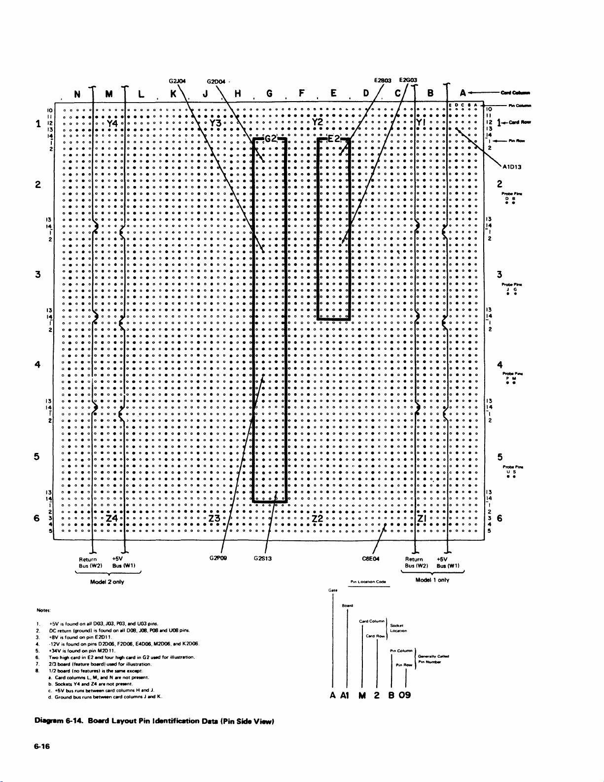
1 12
2
3
4
5
6 3
N
10
o 0
••••••••••••
II
o 0
13
I,!
1
oeoeoo.
2
oeoeoo.
oeo.ooeoeoo
13
14
r
2
o.
o.o.oo.oeoo.o.oo.
o • 0 • 0
oeo.o
13
14
i
2
0.0.00.0.00.0.00.0.
0.0.0
o.o.oo.o.oo.o.oo.oe
o •
o •
13
14
r
2
o.
13
14
I
2
o 0
4
5
o 0
••••••••••••
o •
oeooeoeo
o • 0
oeoeooeo
oeoeooeo
o • 0
o • 0 • 0
oeo.
oeooeoeo
oeo
o
oeoo.oeooeoeoo.
oeooeoeooeoeo
o • 0 • 0
oeo.ooeoeo
0
.0.00.0.00.0.
o.o.ooeoeo
oeo.ooeo.o
o • 0 • 0 • 0
o.oo.o.ooeo.o
o • 0 • 0
0 • 0 0 • 0 • 0 0 • a • 0 0 •
000.000
oeoo.o.oo.oeoo.
• 0 • 0
o • 0 • 0
o.oo.oeooeo.o
0.0.00.0.0
0.0.00.0.0
o.oo.oeo
0.0.00.
o.oeoo.
••••••••••••
o 0 0 0 0 Z40 0 0 0 0 0
••••••••••••
0000000000000
M
Y4
eo.ooeoeo
o.ooeo
oeo
•
0 0
o • 0 • 0
o • 0 • 0
o • 0
oeoeoo.
oeo.oo.
o • 0 • 0
~
• 0
000
L
o • 0
o • 0
.00.0.00.0.00.0
o • 0
G2J04
0
0 0
o •
o •
o •
o •
o • 0 •
0000
0
I<
o •
o •
o •
o •
o •
o •
o 0 •
ooeoeoo
o 0 •
ooeoeoo
00.0.0
o 0 • 0 •
o 0 • 0
o 0 •
••••
G2D04
oeooeo.
eo.ooeoeooeo.
o •
• 0 •
• 0 •
• 0 • a 0
• 0 • 0
a
• 0 •
• 0 •
• 0
eo.oo.o
.o.ooeo
• 0
• 0
• 0 0
.
• 0 •
eooeo.
• 0 0 •
eooeo.
E2B03 E2G03
G
.
•
eo.
o • 0 0 •
F E
o 0 •
oeoo.oeo
oeoeooeoeooeo
o • 0 • 0
oeo.oo.
o • 0 • 0
oeoeooeo.
eoo.oeooeo.
o • 0
0.00.0
o • 0 0 •
0000
0
oeo.ooeo.
• 0 0 •
• 0 0 •
oeoeooeo
o 0 • 0
0.0.00.0.
o.o.ooeo.
o.o.oo.o.ooeo
o.oeooeoe
0.0.00.0.
0.0.00.0.
0.0.00.
o • 0 • 0
o • 0 •
••••••••••••
•••••••••••
o.
•
o • 0 •
• 0 •
o • 0
o • 0
o •
oeoo.oeooeoeoo.
oeooeoeooeoeooecteooeoe
0.00.0.00.0.00.0.00.0.
0.00.0.00.0.00.0.00.0.
0.00.0.00.0.00.0.00
o.ooeo.oo.
eoeoo.
oeooeoeoo.
o.ooeo.oo.
oeoo.oeo
oeooeo.
0000000
00000000
0.00.0.00.0.00.0.00.0.
9.00.0.00.0.00.0.00.0.00eo.o
o.oeoo.o.ooeo.o
o • 0 • 0
00.0.00.0.00.
00.0.0
oo.oeoo.o.ooeo
00.0.00.0.00.0.00.
o •
o 0 •
••••••••••••
o 0 a 0 0 0 Z2 0 0 a a Z I 0 0 0 0 0 0
o
••••••••••••
0.0.00.0.00.0.00.0.00.0.0
o • 0
o • 0 • 0 o • 0
o • 0 • 0
0.00.0.00.
0.00.0
ooeo.o
00.0.0
0.00.0.0080.00.0
a • 0 0 • 0 • 0 0 • 0 • 0 0 • 0 • a 0 •
o.ooeoeo
o.oo.oeooeoeo
000000
eoo.o.o
.oo.oeo
o.
0.0.00.0.00.
o •
oeo.oo.o.o
oe
o •
o •
•
oeoo.o.o
o •
o.
a 0 • a
ooeo.o
o • 0
o 0 • a
• 0
• 0
• 0
• 0
0.0.0
• 0 • 0
o • 0 • 0
o • 0
A
...
·---c:..IIc......
2
• 0
13
14
-I
2
• 0
3
• 0
• 0
13
14
-I
2
• 0
4
13
14
-I
2
5
13
14
-I
0
2
3 6
0
4
5
A1D13
P.-
.....
o 8
· .
_
.....
J G
· .
_PinI
P M
· .
_PiN
U S
· .
Notes:
I.
+5V
IS
found
2.
DC
return (ground) is found on
3.
+8VisfoundonpinE2011.
4.
·12V
is
5.
6. Two high Clrd
7.
8.
Di
found
+J.4VisfoundonpinM2011.
2/3
board
(felture
112
board (no features 1
I.
Card columns
b.
Sock.ts
c. +5V bus runs
d. Ground bus runs
......
m 6-14.
6-16
Return +5V
Bus
(W21
Model 2
on
all
003.
J03.
on
pins
02006.
in
E2
and
four high
boardl used for illustrltion.
is
the _ except:
L.
M,
and
Ind
be_n
Board
Z4
.r.
not
card columns H
be_
N are
Layout
\,,4
Bus (Wl1
only
POJ.
InC! U03 pins.
III
008.
JOB.
F2006.
E4006.
c.d
in G2 used for illustratIon.
not
pre.."t.
~nt.
.nd
card columns J and
P08 InC! U08 pins.
M2D06. and K2D06.
J.
K.
G2P09
Pin Identific8tion D8ta (Pin Side View,
G2S13
Gate
A
A1
C8E04
c.dColumn
I
Card Row
M 2 B
Return +5V
Bus
Socke.
LOUiuon
Pon
Column
""Row
I
09
(W21
Bus
Model 1 only
1:::::-
(WlI
Page 97
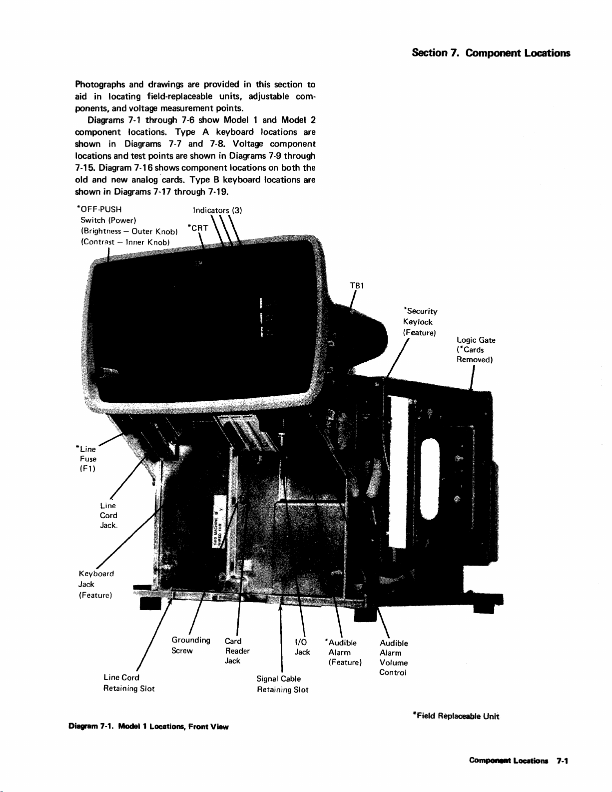
Section 7. Component Locations
Photographs and drawings are provided
aid
in
locating field-replaceable units, adjustable com-
in
this section
to
ponents, and voltage measurement points.
Diagrams
7-1
through 7-6 show Model 1 and Model 2
component locations. Type A keyboard locations are
shown
locations and
in
Diagrams 7-7 and 7-8. Voltage component
test
points are shown
in
Diagrams 7-9 through
7 -15. Diagram 7-16 shows component locations on both the
old and new analog 'cards. Type B keyboard locations are
shown in Diagrams 7-17 through 7-19.
*OFF-PUSH
(Power)
Switch
(Brightness (Contrast -
Outer Knob)
Inner Knob)
Indicators (3)
*Line
Fuse
(F1)
Jack
(Feature)
Line Cord
Retaining
Diagram 7-1.
Modell
Slot
Locations, Front View
Reader Jack
Jack
Signal Cable
Retaining
Slot
Volume
Control
*Field Replaceable Unit
Com
......
Locations 7·1
Page 98
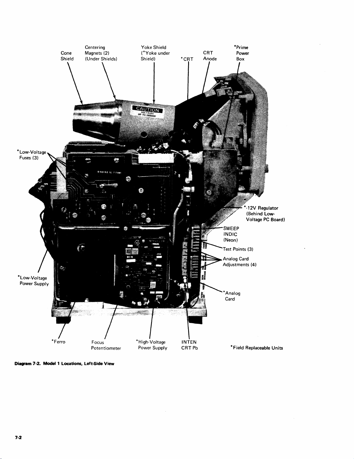
Cone
Shield
Centering
Magnets (2)
(Under Shields)
Yoke Shield
(*Yoke
under
Shield)
*CRT
CRT
Anode
*Prime
Power
Box
* -12V Regulator
(Behind LowVoltage
PC
Board)
*Ferro
Focus
Potentiometer
Diagram 7-2. Model 1 Locations, Left-Side View
*High-Voltage
Power
Supply
INTEN
CRTPb
~==Slj~
Analog Card
Adjustments (4)
*Field
Replaceable
Units
7-2
Page 99

*+5V
Decoupling
Capacitor
*CRT
Yoke
Shield
Cone
Shield
Diagram 7-3. Model 1 Locations. Rear View
*-12V
Regulator
* Arc-
Su
Board
ppression
*Field
Replaceable
Component Locations
Units
7-3
Page 100

+5V
Fuse
AI
(Fl)
+34V
Fuse
AI
(F2)
TB1
Diagram 7-3.1. Location
74
of
+5V and
+34V
Fuses (Model 1)
 Loading...