

Page 1
查询IBM31T1100供应商
IBM31T1100A
Integrated Infrared Transceiver Module
Highlights
x
IrDA 1.1, HP- SIR and Sharp ASK c ompliant
x
Supports IrDA data rates up to 4 Mbps
x
Low pro file (height = 5.6 mm max.)
x
Minimum external components
x
On-chip L ED pro tec tio n c irc uit
x
Low power consumption
x
5 V Supply Voltage
x
Com p le te d ifferential receiver design
x
Am bie n t light and no ise re jection circuitry
x
Shutdown pin for po w er management
x
Programmable bandwidth control
x
Com p a tib le with all major S u p e r I/Os
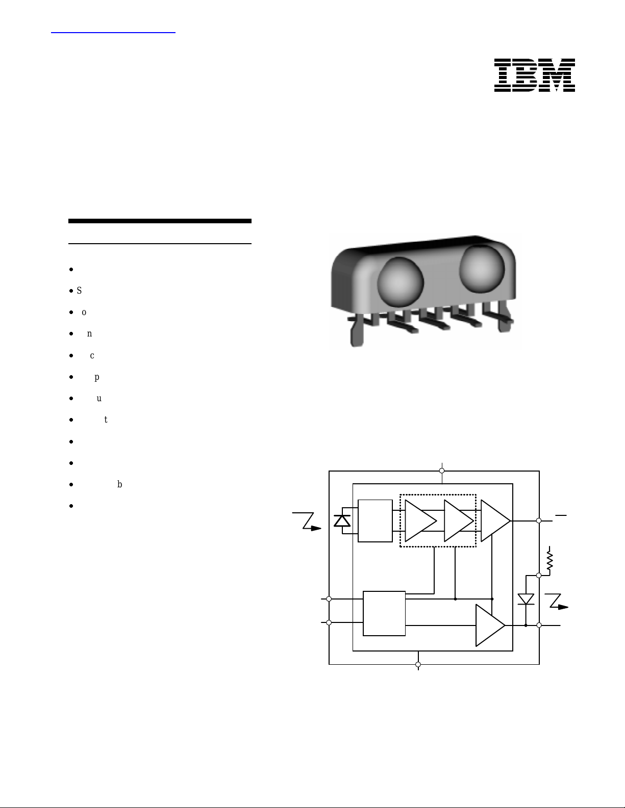
General Description
The IBM31T1100A is a multi-mode integrated
infrared (IR) transceiver module for data
communication systems. The transceiver supports
IrDA speeds up to 4 Mbps, HP-SIR and Sharp ASK
modes. Integrated into this tiny package is a
photodiode, LED and analog transceiver ASIC to
provide a total solution in a single package. A
current limiting resistor in series with the LED and
a Vcc bypass capacitor are the only external
components required to implement a complete
transceiver.
Pack a g e
Noise
Rejection
Circuit
TX
6
7
Control
logic
SD/BW
Block D ia g r a m
Amp
BW
SD
4
GND
3
Vcc
+
Comp
-
Driver
Driver
2
8
1
RX
Vcc
LEDA
LEDC
Page 2
IBM31T1100A
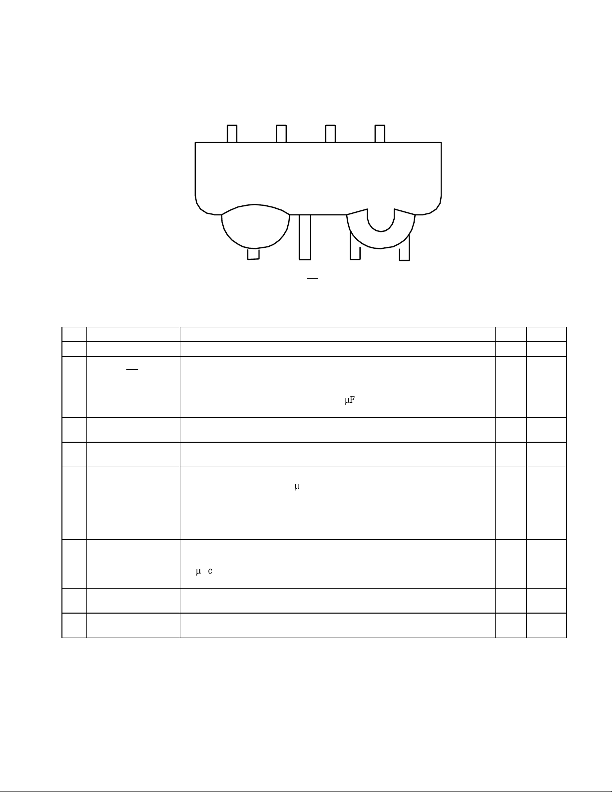
Pin Assignm e nts and De s c riptions
LEDA
8
LED
LEDC
Pin Pin Name Description I/O Active
1
2
3
4 GND Connect to ground of the pow er supply. A solid ground plane is recommended f or proper
5 NC This pin is res erved fo r sp e cial application use only. No signal shou ld b e connected to
6 SD/BW This CMOS input is used to put the IBM31T1 100A in shutdown mode. No m inal supply
7 TX Used to transmit serial data when SD/BW is low. This CMOS input controls the LED
8 LEDA Connect this input to Vc c through a resistor to set the proper LE D current. Add an
LEDC
RX
V
cc
Guide Pins
(not shown above)
Ind icates the state o f the internal L ED cathode. Norm ally not connected. O Lo w
Indicates received serial data. It is a push-pull CMOS driver capable of driving a
standard CMOS or TTL load. No external pull-up or pull-down resisto r is required. May
switch indeterminately when the IBM31T1100A is transmitting.
Connect to + 5 V power supply . Place a 1.0- 10 PF ceramic bypass capacitor as close as
possible to this pin.
operation.
this pin.
current draw in this mode is 35 PA versus 5 mA in normal mode. Together with th e T X
input, this pin also sets the receiver bandwidth. If TX is lo w w hen SD /BW transitions
from high to low, the re ceiver band width is optim ized for operation u p to 1.2 Mbps. If
TX is high when SD /BW transition s from high to low, the receiver b an d width is
optim ized for operation a t 4 Mb p s.
driver. A n on-chip protection c irc uit disables the LED driv er if TX is hig h f or more than
60 Psec. Th is pi n is a lso used to pr ogram th e b a n d width of th e receiver. See SD/B W pin
description.
external LED in series to increase output intensity if required. I
Two through-h ole guide pin s p rovide me chanical stab ility during boar d mounting. They
also improv e heat c onduction when the part is in operation.
TX SD/BW
7
1
2
RX
65
NC
Photodiode
V
CC
43
GND
OLow
IHigh
IHigh
NOTE: The IBM31T1100A is pin and plug com patible with the Temic TFDS6000D.
2
Page 3

IBM31T1100A
Electrical and Timing Specifications
Absolute Maximum Ratings
Symbol Parameter Min Typ Max Unit Condition
V
CC
P
D
T
J
I
LED
Recommended Operating Conditions
Supply Vo ltage R ange - 0.5 6 V
Power Dissipation 450 mW
Junction Temperature 125 °C
Storage Temp erature Rang e - 25 85 °C
Solder ing Tempera tur e 240 °C See application no te s
LED Current 0.8 A <2 µs, ton<10%
Voltage at An y Pin - 0.5 Vcc+ 0.5 V
Symbol Parameter Min Typ Max Unit Condition
V
CC
T
A
DC Electrical C haracteristics
Supply Vo ltage 4.5 5 5.5 V
Operating Temperature Range 0 70 °C
TA = 0 - 70 qC, V
= 5 V r 10 %, unless otherwise specified
CC
Symbol Parameter Min Ty p Max Unit Condition
I
V
V
I
I
LED
V
V
V
C
CC
CC
I
Dynam ic Supply Current 5 7 mA SD = 0 V
Standby Supply C urrent 35 100 uA SD = V
Repetitiv e P u ls ed LED Curre nt 0.55 A < 60 µs, t
RX
OL
OH
IL
IH
IH
L
I
Output Voltage Low @ IOL = 2.5 mA 0.3 0.5 V
RX
Output Voltage High @ -IOH = 2.5 mA V
- 0.5 V
CC
Input Voltage Low (TX, SD/BW) 0 0.8 V
Input Voltag e Hig h (TX ) 3.0 V
Input Voltag e Hig h (SD /BW) V
- 0.5 V
CC
Input Leakage Current - 10 +10 uA
Input Capacitance 5 pF
- 0.5, SC = NC
CC
d
25 %
on
3
Page 4

IBM31T1100A
AC Electrical C haracteristics
TA = 0 - 70 qC, V
= 5 V r 10 %, unless otherwise specified
CC
Symbol Parameter Min Typ Max Unit Condition
t
t
t
t
t
PW
t
PW
t
PW
t
PW
t
t
t
RXEN
t
DIS_LED
Optical Cha ract eris t ics
RX
R
F
S
H
D
L
Rise Time 10 40 ns R
RX
Fall Time 10 40 ns R
TX Setup Time to SD/BW L ow 200 ns
TX Hold Time fro m SD /BW Low 200 ns
RX
Pulse Width 0.8 20 us 9.6 kbps
RX
Pulse Width 100 500 ns 1.2 Mbps
RX
Pulse Width 60 165 ns 4 Mbps
RX
Pulse Width 185 290 ns 4 Mbps double pulse
Output Delay @ Ee = 40 mW/cm
2
12us
Latency 120 us
RX
Valid After Shutdown 60 us
LED C Inac tive Af te r T X High 60 us
TA = 0 - 70 qC, V
= 5 V r 10%, unless otherwise specified
CC
LED
LED
d
1.2 Mbps
= 2.0 K:, C = 50 pF
= 2.0 K:, C = 50 pF
Symbol Parameter Min Typ Max U nit Cond ition
E
E
E
E
emax
Minimum Detection Irradiance (SIR mode) 0.025 0.035 Wm-29.6 - 115 kbps
emin
Minimum Detection Irradiance 0.035 0.05 Wm-21.2 Mbps
emin
Minimum Detection Irradiance 0.07 0.08 Wm-24 Mbps
emin
Maximum Detection Irradiance 5000 Wm-2All spe ed s
100 140 320 (1) mW/sr Tx = High, SD = Low , R
I
Output R ad ia n t Intensity
e
=5.0, D=0 q, D=r15 q, TA=25 qC
V
CC
0.4 uW/sr Tx=Low or SD=High, R
=5.0, D=0 q, D=r15 q, TA=25 qC
V
CC
D
Output R ad ia n t Intensity Half Angle
O
Peak Wavelength 880 900 nm
P
r
24
q
Optical Overshoot 25 %
1. Maximum intensity specified for class 1 operation of IEC 825-1
LED
LED
= 5.6
=5.6
:
:
4
Page 5

IBM31T1100A
700
600
500
400
Min
Max
300
200
F
100
I Forward Current (mA)
2.0 2.2 2.4
VLEDA Forward Voltage (V) - T = 25°C
2.6
A
Figure 1. VLEDA to GND Voltage vs. peak LED current.
175
150
125
Typ
100
Min
75
50
25
Output Intensity in mW/Sr
0.2 0.4 0.6
I Forward Current in Amperes
F
0.8
700
600
500
Min
400
300
200
100
F
I LED Forward Current (mA)
1.5 1.7 1.9
V LED Forward Voltage (V) - T = 25°C
F
Figure 2. LED F orward Voltage vs . C u rre n t
1000
100
10.0
1.0
0.1
0.01
0.001
Input Irrad ia n c e in mW / cm **2
50
100 150
RX pulse width in ns
Max
2.1
A
200
Figure 3. Output Intensity vs. Current
2.4
2.3
2.2
I =430mA
2.1
F
2.0
1.9
1.8
VLEDA to GND Voltage (V)
20
10 30
50 70
40 60
Temperature in °C
Figure 5. VLEDA to GND Voltage vs. Temperature.
80
Figure 4.
RX
pulse width vs. Irradiance - 4 Mbps mode.
175
150
125
I =430mA
100
F
75
50
25
Output Intensity in mW/Sr
20
10 30 50 70
40 60
Temperature in °C
Figure 6. Output Intensity vs. Tem perature
80
5
Page 6

IBM31T1100A
Timing Diagrams
TX
RX
TX
LEDC
50%
50%
Figure 7.
t
L
Latency Timing
t
DIS_LED
50%
50%
V
V
V
V
V
V
Vcc
IH
IL
OH
OL
IH
V
IH
SD/BW
RX
Figure 8
t
PW
IL
RX
RX
.
valid after Shutdown.
50%
50%
t
RXEN
V
IL
50%
V
OH
V
OL
RX
Figure 11.
Figure 9.
t
PW
LED Protec tion T iming
t
RXH
50% 50%
RX
Timing, SIR mode. The output is indeterminate in the
shaded area . S p u rious transition s may occur.
Figure 10.
V
OH
RX
V
OL
Figure 12.
RX
Timing, 1.2 and 4 Mbps mode
t
F
t
R
10%
RX
Rise and F a ll timing measu re ments.
90%
V
OH
V
OL
6
Page 7

IBM31T1100A
Program m ing the Receiver Bandwidth
The IBM31T1100A powers on with the upper li mit of the receiver
bandwidth set to 1.2 Mbps operation. To set the bandwidth for
operation at 4 Mbps, apply timings as shown in Figure 14 to the
SD/BW and the TX inputs. Note that t he internal LED driver is
disabled when SD/BW is active and is not enabled until the next
rising edge of TX. This ensures that the LED(s) will not be active
during bandwidth adjustment. It is recommended that the SD/BW
pin be connected to GND i f bandwid th ad justme nt an d shut down
mode are not used.
To switch the IBM31T 1100A from the def ault state to 4 Mbps and
vice versa, the programming specific atio ns are as f ollows:
SD/BW
TX
(Setting high bandwidth mode)
TX
(Setting low bandwidth mode)
Figure 13. Bandwidth Programming
50%
t
S
50% 50%
t
H
V
IH
V
IL
V
IH
V
IL
V
IL
Setting t h e receiver to 4 M bps m o de
1. Set the SD/BW input to logic hig h.
2. Set the TX input to logic high. Wait t
t 200 ns.
S
3. Set the SD/BW to logic lo w. (This high- to-low tran s ition
latches th e s ta te of TX, w h ich determines th e re ceiver
bandwidth.)
4. After w a itin g t
t 200 ns, set the TX input to logic low. The
H
receiver is now in h igh bandwid th mode, the optimal setting
for 4 Mbps operatio n.
Package Dim e ns ions
5.45 ± 0.5
3.75 ± 0.5
5 ± 3°
Setting t h e receiver to 9.6 kbps-to-1.2 Mbps mode
1. Set the SD/BW input to logic hig h.
2. Ensure that the TX input is at logic low. W ait t
3. Set the SD/BW to logic lo w. (This high- to-low tran s ition
latches th e s ta te of TX, w h ich determines th e re ceiver
bandwidth.)
4. Ensure that the TX input remains low for t
receiver is now in low bandw id th mode, which is the optimal
setting for data rates from 9.6 kbps to 1.2 Mbps.
13 ± 0.5
6.5 ± 0.5
A
0.5
3.3 ± 0.5
3.7 ± 0.5
t 200 ns.
S
t 200 ns. The
H
A
4.0±0.3
5.3 ± 0.3
B
6.7 ± 0.4
0.275 ± 0.075
2.35 ± 0.3
0.5
0.635
0.6 ± 0.2
0.9 ± 0.1
B
0.5 ± 0.1
(7X) 1.27
(2X) 1.45
1.5±0.2
Dimensions in mm.
7
Page 8

IBM31T1100A
Revision History
The following changes have b e e n made in the spe cifications from
the IBM31T1100 data sheet.
1. Impro ved Irradiance values have been updated.
2. LED protec tio n circuit has been added.
3. The
rise time specification is 40 ns instea d of 35 ns.
RX
4. 200K internal pull-down resistor has been removed from the
SD/BW pin.
5. Output Intensity and
pulse width graphs have been
RX
updated.
Order ing I nf ormation
Order Part Number Qty/Reel
IBM31T1100A 750 Pieces
£
¤
Inte rn ati o nal Bus i ne s s M ac h in e s Co rp o rat io n 1995
Printed in the Unite d States of A merica
5-97
All Rights Re se rved
£¥IBM and the IBM logo are registered trademarks of the IBM Corporation.
IBM Microelectronics is a trademark of the IBM Corporation.
Hewlett-Packard is a registered trademark of Hewlett-Packard Corporation.
Sharp is a trademark of Sharp Electronics Corporation.
All other registered trademarks and trademarks are the properties of their
respective companies.
The information provided is believed to be accurate and reliable. IBM
reserves the right to make changes to the product described without notice.
No liability is assumed as a result of its use nor f or any infring eme nt of the
rights of others.
This document may contain preliminary information and is subject to
change by IBM without notice. IBM assumes no responsibility of liability
for any use of the information contained herein. Nothing in this document
shall operate as an express or implied license or indemnity under the
intellectual property rights of IBM or third parties. The products described
in this document are not intended for use in implantation or other direct life
support applications where malfunction may result in direct physical harm
or injury to pe rso ns . NO W AR RANTIES OF ANY K IND, INCLU DING,
BUT NOT LIMITED TO, THE IMPLIED WARRA NTIES OF
MERCHANTABILITY OR FITNESS FOR A PARTICULAR
PURPOSE ARE OFF ERED IN THIS DOCU MENT.
IBM Microelectronics Division
1580 Route 52, Bl dg . 504
Hopewell Junction, NY
12533-6531
The IBM home page can be found at http://www.ibm.com
The IBM Microelectronics Division home page can be found at
http://www.chips.ibm.com
GH45-5286-01
8
 Loading...