


MI930/MI930F
AMD Athlon™ 64 / Athlon™ 64 x2
(Dual Core) / Sempron™
Mini-ITX Motherboard
USER’S MANUAL
Version 1.0A

ii
MI930 User’s Manual
Acknowledgments
Award is a registered trademark of Award Software International,
Inc.
PS/2 is a trademark of International Business Machines
Corporation.
AMD Athlon™ 64 / Athlon™ 64 x2 (dual core) / Sempron™
processors are registered trademarks of AMD Corporation.
Microsoft Windows is a registered trademark of Microsoft
Corporation.
Winbond is a registered trademark of Winbond Electronics
Corporation.
All other product names or trademarks are properties of their
respective owners.

MI930 User’s Manual iii
Table of Contents
Introduction ....................................................... 1
Product Description ............................................................. 1
Checklist .............................................................................. 2
MI930 Specifications .......................................................... 3
Board Dimensions ............................................................... 4
Installations ....................................................... 5
Installing the CPU ............................................................... 6
Installing the Memory ......................................................... 7
Setting the Jumpers ............................................................. 8
Connectors on MI930 ........................................................ 12
BIOS Setup ....................................................... 23
Drivers Installation ...................................... 41
SM Bus Controller Driver Installation .............................. 42
VGA Drivers Installation .................................................. 45
Realtek Codec Audio Driver Installation .......................... 47
LAN Drivers Installation ................................................... 50
Appendix ........................................................... 51
A. I/O Port Address Map ................................................... 51
B. Interrupt Request Lines (IRQ) ...................................... 52
C. Watchdog Timer Configuration .................................... 53

iv
MI930 User’s Manual
This page is intentionally left blank.

INTRODUCTION
MI930 User’s Manual 1
Introduction
Product Description
The MI930 Mini ITX board incorporates the Mobile AMD M690T Express
Chipset for Embedded Computing, consisting of the AMD M690T (North
Bridge) and SB600 (South Bridge), an optimized integrated graphics solution
with an 800MHz front-side bus. Dimensions of the board are 170mm x 170mm.
The M690T integrates an ATi Radeon X700-based graphics engine supporting
dual display, an LVDS interface, an integrated TMDS controller, and operates at
core speeds of up to 400 MHz. MI930 features a low-power design, is validated
with the AMD Athlon™ 64 / Athlon™ 64 x2 (dual core) / Sempron™ on 65nm
process. With two dual channel DDR2 800MHz DIMM sockets on board, the
board supports up to 4GB of DDR2 system memory.
The main features of the board are:
Supports AMD Athlon™ 64 / Athlon™ 64 x2 (dual core) / Sempron™
Supports up to 2.8GHz, 800MHz FSB
Two DDR2 SDRAM DIMM, Max. 4GB memory
2x Marvell PCI-Express Gigabit LAN
AMD M690T Express VGA for CRT / LVDS / DVI
2x SATA, 6x USB 2.0, 2x COM, Watchdog timer
1x PCI slot (expansion to two PCI slots)

INTRODUCTION
2
MI930 User’s Manual
Checklist
Your MI930 package should include the items listed below.
• The MI930 Mini-ITX motherboard
• This User’s Manual
• 1 CD containing chipset drivers and flash memory utility
• Cable kit (IDE, Serial port, Serial ATA)

INTRODUCTION
MI930 User’s Manual 3
MI930 Specifications
CPU Supported
AMD Athlon™ 64 / Athlon™ 64 x2 (dual core) / Sempron™ 64-bit
processor integrated w/ DDRII memory controller in CPU.
CPU Voltage
0.700V ~ 1.5V
System Speed
Up to 2.8GHz or above
CPU FSB
800MHz FSB
Cache
128K/256K/512K1MB/2MB
Green /APM
APM1.2
CPU Socket
Socket AM2 (940pin)
Chipset
ATI M690T / SB600 chipset
NB: M690T, 465-ball FCBGA (21x21mm)
SB: ATi SB600, 549-ball FCBGA (23x23mm, 0.8mm pitch)
BIOS
Award BIOS, support ACPI Function
Memory
DDR2 800/667/533 SDRAM DIMM x2 (w/o ECC function), Max. 4GB
VGA
ATi M690T built-in Radeon X700 based graphic engine, supports full
DirectX9.0. RS690T integrates TMDS controller for DVI and 18 or
24-bit LVDS interface. Supports dual display for below display
combinations:
- Analog (CRT) + digital (DVI or LVDS)
- Both digital (DVI + LVDS)
LAN
Marvell 88E8053 PCI-e Gigabit LAN controller x2
USB
ATi SB600 built-in USB 2.0 host controller, support 6 ports
Serial ATA Ports
ATi SB600 built-in SATA II (3.0Gb/sec) host controller, supports 2
ports and RAID 0, 1 function
Parallel IDE
ATi SB600 built-in one channel Ultra DMA 33/66/100/133
Audio
ATi SB600 built-in audio controller + AC97 Codec ALC888 w/ 7.1
channels
LPC I/O
W83627EHG: COM1 (RS232), COM2 (RS232/422/485) & hardware
monitor (3 thermal inputs, 4 voltage monitor inputs, 2 fan headers).
Parallel, IrDA & Floppy not used
Digital IO
4 in & 4 out
Keyboard/Mouse
Supports PS/2 keyboard/mouse connector
Expansion Slots
PCI slot (32bits/33MHz) x1
8x2 pin-header x1 for LPC TPM adaptor card (reserved) or
8x2 pin-header x1 for LPC 2
nd
I/O adaptor card COM3 /COM4
(RS232) or COM3 /COM4 /COM5 /COM6 (RS232) (reserved)
Edge Connector
PS/2 connector x1 for keyboard/mouse
DB9 & DVI stack connector x1 for COM 1 and DVI
RJ-45 + dual USB stack connector x2 for LAN1, 2 & USB1~4
RCA jack 3x1 for audio (Line-in, Line-Out, Mic.) & pin header for front
panel (Line-Out2, Mic2)
Onboard Header/
Connector
DF13-20 x2 for LVDS
40-pin, 2.54mm, box-header x 1 for IDE1
5x2 pin-header x1 for USB5~6
5x2 pin-header x1 for front audio (headphone & Mic.)
10 pin-header x1 for COM2
8x2 pin-header x1 for VGA
Watchdog Timer
Yes (256 segments, 0, 1, 2…255 sec/min)
System Voltage
+5V, +3.3V, +12V, -12V, 5VSB (2A)
Others
Modem Wakeup, LAN Wakeup
Board Size
170mm x 170mm (Mini ITX)

INTRODUCTION
[
Board Dimensions
4
MI930 User’s Manual

INSTALLATIONS
MI930 User’s Manual 5
Installations
This section provides information on how to use the jumpers and
connectors on the MI930 in order to set up a workable system. The
topics covered are:
Installing the CPU ........................................................................ 6
Installing the Memory .................................................................. 7
Setting the Jumpers ...................................................................... 8
Connectors on MI930 ................................................................ 12

INSTALLATIONS
Installing the CPU
The MI930 board supports a Socket AM2 (940-pin) processor socket for
AMD
Athlon™ 64 / Athlon™ 64 x2 (dual core) / Sempron™ processors.
To install the CPU, unlock first the socket by pressing the lever
sideways, then lift it up to a 90 degree angle as shown below. Then,
position the CPU above the socket such that the CPU corner ali gns wi th
the gold triangle matching the socket corner with a small triangle.
Carefully insert the CPU into the socket and push down the lever to
secure the CPU. Then, install the heatsink and fan.
NOTE:
Ensure that the CPU heat sink and the CPU top surface are in
total contact to avoid CPU overheating problem that would
cause your system to hang or be unstable.
6
MI930 User’s Manual

INSTALLATIONS
Installing the Memory
The MI930 board supports two DDR2 memory socket for a maximum
total memory of 4GB in DDR2 memory type.
Installing and Removing Memory Modules
To install the DDR2 modules, locate the memory slot on the board and
perform the following steps:
1. Hold the DDR2 module so that the key of the DDR2 module aligned
with that on the memory slot.
2. Gently push the DDR2 module in an upright position until the clips of
the slot close to hold the DDR2 module in place when the DDR2
module touches the bottom of the slot.
3. To remove the DDR2 module, press the clips with both hands.
DDR2 Module
Lock Lock
Lock Lock
MI930 User’s Manual 7

INSTALLATIONS
8
MI930 User’s Manual
Setting the Jumpers
Jumpers are used on MI930 to select various settings and features
according to your needs and applications. Contact your supplier if you
have doubts about the best configuration for your needs. The following
lists the connectors on MI930 and their respective functions.
Jumper Locations on MI930 ........................................................... 9
JBAT1: Clear CMOS Setting ....................................................... 10
JP1: LCD Panel Power Selection.................................................. 10
JP2: PCI Riser Card Selection ...................................................... 10
JP3, JP4, JP5: RS232/422/485 (COM2) Selection ....................... 11

INSTALLATIONS
Jumper Locations on MI930
Jumpers on MI930 ............................................................................ Page
JP1: LCD Panel Power Selection ................................................. 10
JP2: PCI Riser Card Selection ...................................................... 10
JBAT1: Clear CMOS Setting ....................................................... 11
MI930 User’s Manual 9

INSTALLATIONS
JBAT1: Clear CMOS Setting
JBAT1 Setting
Normal
Clear CMOS
JP1: LCD Panel Power Selection
JP1 LCD Panel Power
3.3V
5V
JP2: PCI Riser Card Selection
JP2 Riser Card
IP390 Riser Card
Install
IP151, IP240 Riser Card
Install
10
MI930 User’s Manual

INSTALLATIONS
JP3, JP4, JP5: RS232/422/485 (COM2) Selection
COM1 is fixed for RS-232 use only.
COM2 is selectable for RS232, RS-422 and RS-485.
The following table describes the jumper settings for COM2 selection.
COM2
Function
RS-232 RS-422 RS-485
Jumper
Setting
(pin closed)
JP5:
1-2
JP4:
3-5 & 4-6
JP3:
3-5 & 4-6
JP5:
3-4
JP4:
1-3 & 2-4
JP3:
1-3 & 2-4
JP5:
5-6
JP4:
1-3 & 2-4
JP3:
1-3 & 2-4
COM2 is jumper selectable for RS-232, RS-422 and RS-485.
Pin # Signal Name
RS-232 R2-422 RS-485
1 DCD TX- DATA2 RX TX+ DATA+
3 TX RX+ NC
4 DTR RX- NC
5 Ground Ground Ground
6 DSR RTS- NC
7 RTS RTS+ NC
8 CTS CTS+ NC
9 RI CTS- NC
10 NC NC NC
MI930 User’s Manual 11

INSTALLATIONS
12
MI930 User’s Manual
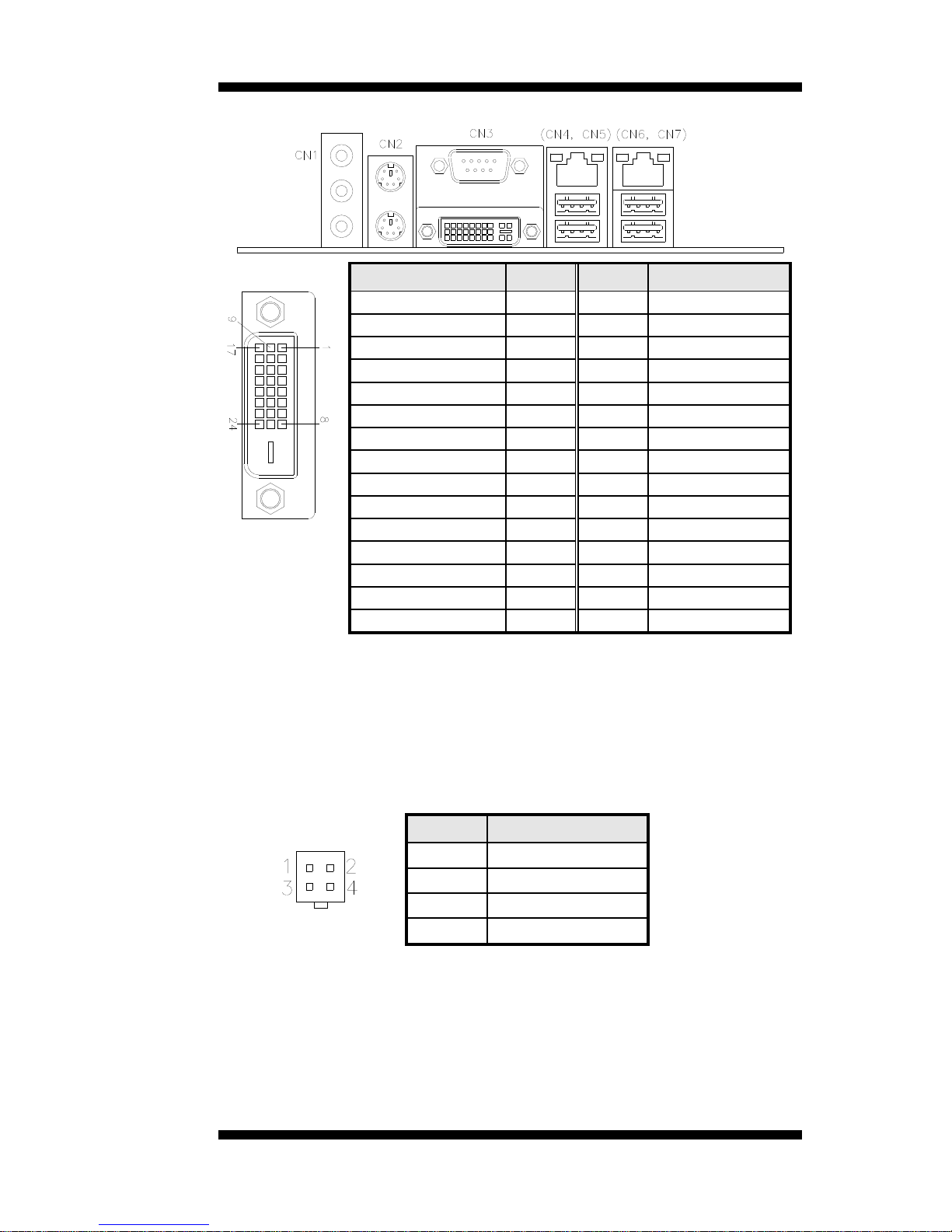
Connectors on MI930
Connector Locations on MI930 ........................................................... 13
CN1: Audio Connector ........................................................................ 14
CN2: PS/2 Keyboard and PS/2 Mouse Connectors ............................. 14
CN3: COM1 and DVI-I Connector ..................................................... 14
CN4, CN5: GbE RJ45 (MI930) and USB1/2 Ports ............................. 15
CN6, CN7: GbE RJ-45 (MI930F) and USB3/4 Ports .......................... 15
ATX1: ATX 12V Power Connector .................................................... 15
ATX2: ATX Power Supply Connector ................................................ 16
FAN1: System Fan Power Connector .................................................. 16
FAN2: CPU Fan Power Connector ...................................................... 16
F_USB1: USB0/USB1 Connector ....................................................... 16
IDE1: IDE Connector .......................................................................... 17
SATA1, SATA2: SATA Connectors ................................................... 17
COM2: COM2 Serial Port ................................................................... 17
LVDS1, LVDS2: LVDS Connectors (1st channel, 2nd channel) ........ 18
J2: Audio Pin Header for Chassis Front Panel..................................... 18
J3: CD-In Pin Header ........................................................................... 18
J4: For LPC I/F Adaptor Card ............................................................. 18
ID394 with Fintek F81216, 2 or 4 Serial Ports .................................... 18
ID395 Winbond WPCT200 x1 for TPM1.2 ........................................ 18
J5: SPI Flash Connector (factory use only) ......................................... 18
J6: Power LED Connector ................................................................... 18
J7 (F_PANEL): System Function Connector ...................................... 19
J8: LCD Backlight Connector .............................................................. 19
J9: Digital I/O ...................................................................................... 20
PCI1: PCI Slot (supports 2 Master) ..................................................... 20
ID395 WINBOND WPCT200 for TPM1.2 ......................................... 20
ID394 LPC Serial Ports Adaptor Card ................................................ 21

INSTALLATIONS
Connector Locations on MI930
Connector Locations on MI930
CN1: Audio Connector ............................................................................................................................. 14
CN2: PS/2 Keyboard and PS/2 Mouse Connectors .................................................................................. 14
CN3: COM1 and DVI-I Connector .......................................................................................................... 14
CN4, CN5: GbE RJ45 (MI930) and USB1/2 Ports .................................................................................. 15
CN6, CN7: GbE RJ-45 (MI930F) and USB3/4 Ports .............................................................................. 15
ATX1: ATX 12V Power Connector ......................................................................................................... 15
ATX2: ATX Power Supply Connector .................................................................................................... 16
FAN1: System Fan Power Connector ...................................................................................................... 16
FAN2: CPU Fan Power Connector .......................................................................................................... 16
F_USB1: USB0/USB1 Connector ............................................................................................................ 16
IDE1: IDE Connector ............................................................................................................................... 17
SATA1, SATA2: SATA Connectors ....................................................................................................... 17
COM2: COM2 Serial Port ........................................................................................................................ 17
LVDS1, LVDS2: LVDS Connectors (1st channel, 2nd channel) ............................................................ 18
J2: Audio Pin Header for Chassis Front Panel ......................................................................................... 18
J3: CD-In Pin Header ............................................................................................................................... 18
J4: For LPC I/F Adaptor Card .................................................................................................................. 18
ID394 with Fintek F81216, 2 or 4 Serial Ports ........................................................................................ 18
ID395 Winbond WPCT200 x1 for TPM1.2 ............................................................................................. 18
J5: SPI Flash Connector (factory use only) .............................................................................................. 18
J6: Power LED Connector ........................................................................................................................ 18
J7 (F_PANEL): System Function Connector ........................................................................................... 19
J8: LCD Backlight Connector .................................................................................................................. 19
J9: Digital I/O ........................................................................................................................................... 20
MI930 User’s Manual 13

INSTALLATIONS
CN1: Audio Connector
CN2: PS/2 Keyboard and PS/2 Mouse Connectors
PS/2 Mouse
PS/2 Keyboard
Signal Name Keyboard Mouse Signal Name
Keyboard data 1 1 Mouse data
N.C. 2 2 N.C.
GND 3 3 GND
5V 4 4 5V
Keyboard clock 5 5 Mouse clock
N.C. 6 6 N.C.
CN3: COM1 and DVI-I Connector
[
Signal Name Pin # Pin # Signal Name
DCD 1 6 DSR
RXD 2 7 RTS
TXD 3 8 CTS
DTR 4 9 RI
GND 5 10 Not Used
14
MI930 User’s Manual
INSTALLATIONS
Signal Name Pin # Pin # Signal Name
DATA 2- 1 16 HOT POWER
DATA 2+ 2 17 DATA 0Shield 2/4 3 18 DATA 0+
DATA 4- 4 19 SHIELD 0/5
DATA 4+ 5 20 DATA 5-
DDC CLOCK 6 21 DATA 5+
DDC DATA 7 22 SHIELD CLK
VSYNC 8 23 CLOCK -
DATA 1- 9 24 CLOCK +
DATA 1+ 10 C1 N.C.
SHIELD 1/3 11 C2 N.C.
DATA 3- 12 C3 N.C.
DATA 3+ 13 C4 N.C.
DDC POWER 14 C5 N.C.
A GROUND 1 15 C6 N.C.
CN4, CN5: GbE RJ45 (MI930) and USB1/2 Ports
CN6, CN7: GbE RJ-45 (MI930F) and USB3/4 Ports
ATX1: ATX 12V Power Connector
This connector supplies the CPU operation voltage
Pin # Signal Name
1 Ground
2 Ground
3 +12V
4 +12V
MI930 User’s Manual 15

INSTALLATIONS
ATX2: ATX Power Supply Connector
11 1
20 10
Signal Name Pin # Pin # Signal Name
3.3V 11 1 3.3V
-12V 12 2 3.3V
Ground 13 3 Ground
PS-ON 14 4 +5V
Ground 15 5 Ground
Ground 16 6 +5V
Ground 17 7 Ground
-5V 18 8 Power good
+5V 19 9 5VSB
+5V 20 10 +12V
FAN1: System Fan Power Connector
FAN1 is a 3-pin header for system fans. The fan must be a 12V
(500mA).
Pin # Signal Name
1 Ground
2 +12V
3 Rotation detection
FAN2: CPU Fan Power Connector
FAN2 is a 4-pin header for the CPU fan. The fan must be a 12V fan.
Pin # Signal Name
4 Control
3 Sense
2 +12V
1 Ground
F_USB1: USB0/USB1 Connector
Signal Name Pin Pin Signal Name
Vcc 1 2 Vcc
D0- 3 4 D1-
D0+ 5 6 D1+
Ground 7 8 Ground
NC 9 10 Ground
Note: This USB connector is compatible with USB 2.0 devices only.
16
MI930 User’s Manual

INSTALLATIONS
IDE1: IDE Connector
Signal Name Pin # Pin # Signal Name
Reset IDE 1 2 Ground
Host data 7 3 4 Host data 8
Host data 6 5 6 Host data 9
Host data 5 7 8 Host data 10
Host data 4 9 10 Host data 11
Host data 3 11 12 Host data 12
Host data 2 13 14 Host data 13
Host data 1 15 16 Host data 14
Host data 0 17 18 Host data 15
Ground 19 20 Protect pin
DRQ0 21 22 Ground
Host IOW 23 24 Ground
Host IOR 25 26 Ground
IOCHRDY 27 28 Host ALE
DACK0 29 30 Ground
IRQ14 31 32
N
o connec
t
Address 1 33 34
N
o connec
t
Address 0 35 36 Address 2
Chip select 0 37 38 Chip select 1
Activit
y
39 40 Ground
SATA1, SATA2: SATA Connectors
COM2: COM2 Serial Port
Pin # Signal Name
RS-232 R2-422 RS-485
1 DCD TX- DATA2 RX TX+ DATA+
3 TX RX+ NC
4 DTR RX- NC
5 Ground Ground Ground
6 DSR RTS- NC
7 RTS RTS+ NC
8 CTS CTS+ NC
9 RI CTS- NC
10 NC NC NC
MI930 User’s Manual 17

INSTALLATIONS
LVDS1, LVDS2: LVDS Connectors (1st channel, 2nd channel)
Signal Name Pin # Pin # Signal Name
TX0- 2 1 TX0+
Ground 4 3 Ground
TX1- 6 5 TX1+
5V/3.3V 8 7 Ground
NA 10 9 NA
TX2- 12 11 TX2+
Ground 14 13 Ground
TXC- 16 15 TXC+
5V/3.3V 18 17 ENABKL
+12V 20 19 +12V
J2: Audio Pin Header for Chassis Front Panel
Signal Name Pin Pin Signal Name
MIC2-L 1 2 Ground
MIC2-R- 3 4 +3.3V
LINE2-R 5 6 MIC2_JD
Front Sense 7 8 NC
LINE2-L 9 10 LINE2_JD
J3: CD-In Pin Header
Pin # Signal Name
1 CD Audio R
2 Ground
3 Ground
4 CD Audio L
J4: For LPC I/F Adaptor Card
ID394 with Fintek F81216, 2 or 4 Serial Ports
ID395 Winbond WPCT200 x1 for TPM1.2
J5: SPI Flash Connector (factory use only)
J6: Power LED Connector
Pin # Signal Name
1 LED+
2 No connect
3 Ground
18
MI930 User’s Manual

INSTALLATIONS
MI930 User’s Manual 19
J7 (F_PANEL): System Function Connector
ATX Power ON Switch: Pins 1 and 2
This 2-pin connector is an “ATX Power Supply On/Off Switch” on the
system that connects to the power switch on the case. When pressed, the
power switch will force the system to power on. When pressed again, it
will force the system to power off.
Hard Disk Drive LED Connector: Pins 3 and 4
This connector connects to the hard drive activity LED on control panel.
This LED will flash when the HDD is being accessed.
Pin # Signal Name
4 HDD Active
3 5V
Reset Switch: Pins 5 and 6
The reset switch allows the user to reset the system without turning the
main power switch off and then on again. Orientation is not required
when making a connection to this header.
+5V and 5VSB Signals: Pins 7 and 8
Pin # Signal Name
7 +5V
8 +5VSB
J8: LCD Backlight Connector
Pin # Signal Name
1 +12V
2 Backlight Enable
3 Ground

INSTALLATIONS
J9: Digital I/O
Signal Name Pin Pin Signal Name
GND 1 2 VCC
OUT3 3 4 OUT1
OUT2 5 6 OUT0
IN3 7 8 IN1
IN2 9 10 IN0
PCI1: PCI Slot (supports 2 Master)
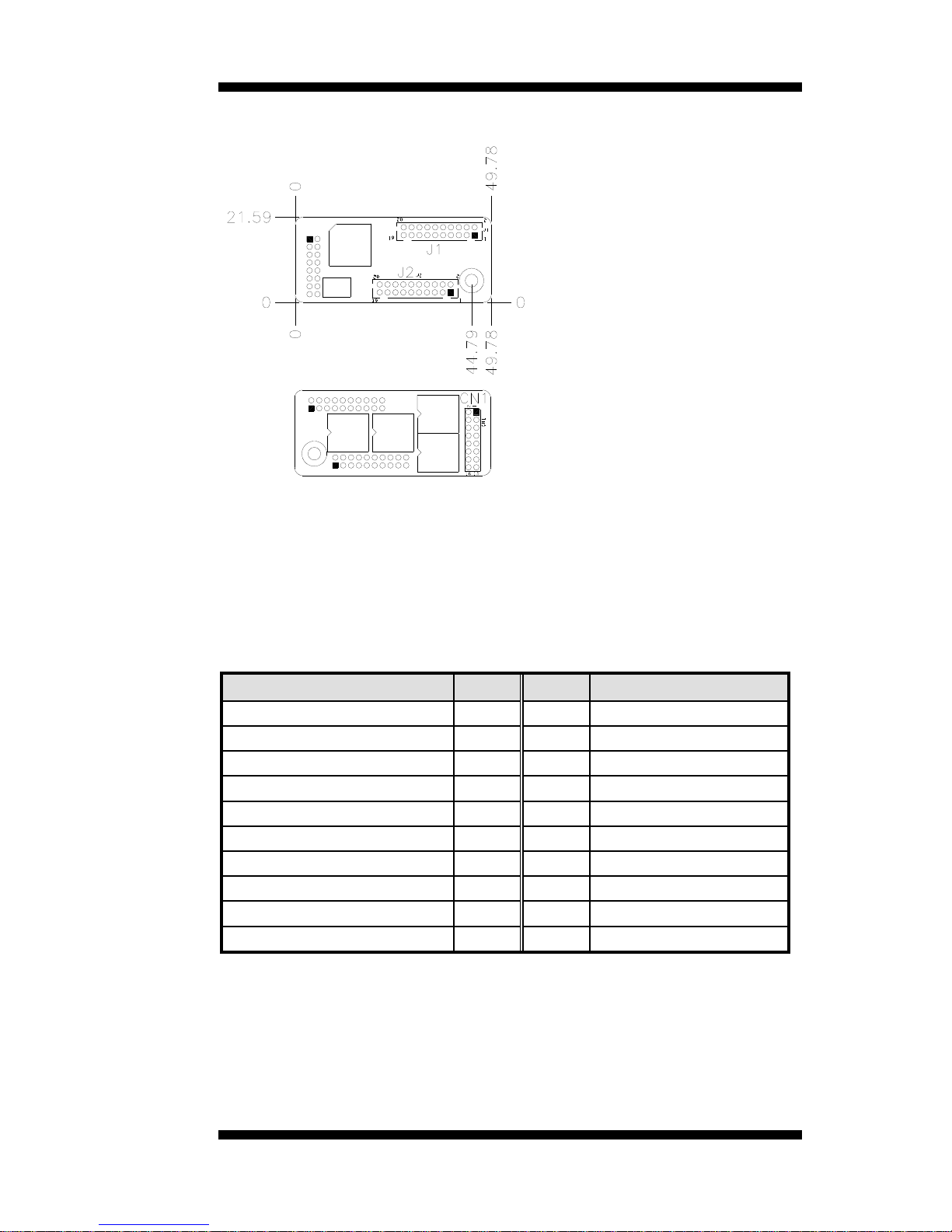
ID395 WINBOND WPCT200 for TPM1.2
CN1: LPC I/F connectors
Package list
Nylon Nut x 1
Screw x 2
Washer x2
20
MI930 User’s Manual
INSTALLATIONS
ID394 LPC Serial Ports Adaptor Card
J1 J2: COM3/4/5/6 Serial Ports
J1 - COM3/4 pin-header connector.
PIN1~PIN10 COM3
PIN11~PIN20 COM4
J2 - COM5/6 pin-header connector.
PIN1~PIN10 COM5
PIN11~PIN20 COM6
Signal Name Pin # Pin # Signal Name
DCD, Data carrier detect 1 2 DSR, Data set ready
RXD, Receive data 3 4 RTS, Request to send
TXD, Transmit data 5 6 CTS, Clear to send
DTR, Data terminal ready 7 8 RI, Ring indicator
GND, ground 9 10 Not Used
DCD, Data carrier detect 11 12 DSR, Data set ready
RXD, Receive data 13 14 RTS, Request to send
TXD, Transmit data 15 16 CTS, Clear to send
DTR, Data terminal ready 17 18 RI, Ring indicator
GND, ground 19 20 Not Used
CN1: LPC I/F connectors
Package list:
COM port cable (PK1-20B) x 2
Nylon Nut x 1
Screw x 2
Washer x2
MI930 User’s Manual 21

INSTALLATIONS
22
MI930 User’s Manual
This page is intentionally left blank.

BIOS SETUP
MI930 User’s Manual 23
BIOS Setup
This chapter describes the different settings available in the Award
BIOS that comes with the board. The topics covered in this chapter are
as follows:
BIOS Introduction ........................................................................ 24
BIOS Setup ................................................................................... 24
Standard CMOS Setup ................................................................. 26
Advanced BIOS Features ............................................................. 28
Advanced Chipset Features .......................................................... 31
Integrated Peripherals ................................................................... 33
Power Management Setup ............................................................ 35
PNP/PCI Configurations .............................................................. 37
PC Health Status ........................................................................... 38
Frequency/Voltage Control .......................................................... 39
Load Fail-Safe Defaults ................................................................ 40
Load Optimized Defaults ............................................................. 40
Set Supervisor/User Password ...................................................... 40
Save & Exit Setup ........................................................................ 40
Exit Without Saving ..................................................................... 40

BIOS SETUP
24
MI930 User’s Manual
BIOS Introduction
The Award BIOS (Basic Input/Output System) installed in your
computer system’s ROM supports various processors. The BIOS
provides critical low-level support for a standard device such as disk
drives, serial ports and parallel ports. It also adds virus and password
protection as well as special support for detailed fine-tuning of the
chipset controlling the entire system.
BIOS Setup
The Award BIOS provides a Setup utility program for specifying the
system configurations and settings. The BIOS ROM of the system stores
the Setup utility. When you turn on the computer, the Award BIOS is
immediately activated. Pressing the <Del> key immediately allows you
to enter the Setup utility. If you are a little bit late p ressing the <Del>
key, POST (Power On Self Test) will continue with its test routines, thus
preventing you from invoking the Setup. If you still wish to enter Setup,
restart the system by pressing the ”Reset” button or simultaneously
pressing the <Ctrl>, <Alt> and <Delete> keys. You can also restart by
turning the system Off and back On again. The following message will
appear on the screen:
Press <DEL> to Enter Setup
In general, you press the arrow keys to highlight items, <Enter> to
select, the <PgUp> and <PgDn> keys to change entries, <F1> for help
and <Esc> to quit.
When you enter the Setup utility, the Main Menu screen will appear on
the screen. The Main Menu allows you to select from various setup
functions and exit choices.

BIOS SETUP
MI930 User’s Manual 25
Phoenix - AwardBIOS CMOS Setup Utility
Standard CMOS Features Frequency/Voltage Control
Advanced BIOS Features Load Fail-Safe Defaults
Advanced Chipset Features Load Optimized Defaults
Integrated Peripherals Set Supervisor Password
Power Management Setup Set User Password
PnP/PCI Configurations Save & Exit Setup
PC Health Status Exit Without Saving
ESC : Quit Ç È Æ Å : Select Item
F10 : Save & Exit Setup
Time, Date, Hard Disk Type…
The section below the setup items of the Main Menu displays the control
keys for this menu. At the bottom of the Main Menu just below the
control keys section, there is another section, which displays information
on the currently highlighted item in the list.
Note:
If the system cannot boot after making and saving system
changes with Setup, the Award BIOS supports an override to
the CMOS settings that resets your system to its default.
Warning:
It is strongly recommended that you avoid making any
changes to the chipset defaults. These defaults have been
carefully chosen by both Award and your system
manufacturer to provide the absolute maximum performance
and reliability. Changing the defaults could cause the system
to become unstable and crash in some cases.

BIOS SETUP
26
MI930 User’s Manual
Standard CMOS Setup
“Standard CMOS Setup” choice allows you to record some basic
hardware configurations in your computer system and set the system
clock and error handling. If the motherboard is already installed in a
working system, you will not need to select this option. You will need to
run the Standard CMOS option, however, if you change your system
hardware configurations, the onboard battery fails, or the configuration
stored in the CMOS memory was lost or damaged.
Phoenix - AwardBIOS CMOS Setup Utility
Standard CMOS Features
Date (mm:dd:yy) Wed, Apr 28, 2007 Item Help
Time (hh:mm:ss) 00 : 00 : 00 Menu Level >
IDE Channel 0 Master None Change the day, month,
Year and century IDE Channel 0 Slave None
IDE Channel 2Master None
IDE Channel 2 Slave None
IDE Channel 3 Master None
IDE Channel 3 Slave None
Halt On No Errors
Base Memory 640K
Extended Memory 129024K
Total Memory 130048K
At the bottom of the menu are the control keys for use on this menu. If
you need any help in each item field, you can press the <F1> key. It will
display the relevant information to help you. The memory display at the
lower right-hand side of the menu is read-only. It will adjust
automatically according to the memory changed. The following
describes each item of this menu.
Date
The date format is:
Day : Sun to Sat
Month : 1 to 12
Date : 1 to 31
Year : 1999 to 2099

BIOS SETUP
MI930 User’s Manual 27
To set the date, highlight the “Date” field and use the PageUp/
PageDown or +/- keys to set the current time.
Time
The time format is:
Hour : 00 to 23
Minute : 00 to 59
Second : 00 to 59
To set the time, highlight the “Time” fi eld and use the <PgUp>/ <PgDn>
or +/- keys to set the current time.
IDE Channel Master/Slave
The onboard PCI IDE connector provides Primary and Secondary
channels for connecting up to two IDE hard disks or other IDE devices.
Press <Enter> to configure the hard disk. The selections include Auto,
Manual, and None. Select ‘Manual’ to define the drive information
manually. You will be asked to enter the following items.
CYLS : Number of cylinders
HEAD : Number of read/write heads
PRECOMP : Write precompensation
LANDING ZONE : Landing zone
SECTOR : Number of sectors
Remarks: The main board supports two serial ATA ports and are
represented in this setting as IDE Channel 0.
Halt On
This field determines whether or not the system will halt if an error is
detected during power up.
No errors The system boot will not be halted for any error
that may be detected.
All errors Whenever the BIOS detects a non-fatal error,
the system will stop and you will be prompted.
All, But Keyboard The system boot will not be halted for a
keyboard error; it will stop for all other errors
All, But Diskette The system boot will not be halted for a disk
error; it will stop for all other errors.
All, But Disk/Key The system boot will not be halted for a key-
board or disk error; it will stop for all others.

BIOS SETUP
28
MI930 User’s Manual
Advanced BIOS Features
This section allows you to configure and improve your system and
allows you to set up some system features according to your preference.
Phoenix - AwardBIOS CMOS Setup Utility
Advanced BIOS Features
CPU Feature Press Enter ITEM HELP
Hard Disk Boot Priority Press Enter
Virus Warning Disabled Menu Level >
USB Hard Disk Boot First Disabled
CPU Internal Cache Enabled
External Cache Enabled
Quick Power On Self Test Enabled
First Boot Device Hard Disk
Second Boot Device CDROM
Third Boot Device LS120
Boot Other Device Enabled
Boot Up Floppy Seek Disabled
Boot Up NumLock Status On
Gate A20 Option Fast
Typematic Rate Setting Disabled
Typematic Rate (Chars/Sec) 6
Typematic Delay (Msec) 250
Security Option Setup
APIC Mode Enabled
MPS Version Control for OS 1.4
OS Select For DRAM>64MB Non-OS2
HDD S.M.A.R.T. Capability Disabled
CPU Feature
Press Enter to configure the settings relevant to CPU Feature.
Hard Disk Boot Priority
With the field, there is the option to choose, aside from the hard disks connected,
“Bootable add-in Cards” which refers to other external devices.
Virus Warning
If this option is enabled, an alarm message will be displayed when trying to write
on the boot sector or on the partition table on the disk, which is typical of the
virus.
CPU Internal and External Cache
Cache memory is additional memory that is faster than conventional DRAM
(system memory). CPUs from 486-type on up contain internal cache memory,
and most, but not all, modern PCs have additional (external) cache memory.
When the CPU requests data, the system transfers the requested data from the
main DRAM into cache memory, for even faster access by the CPU. These allow
you to enable (speed up memory access) or disable the cache function.

BIOS SETUP
MI930 User’s Manual 29
Quick Power On Self Test
When enabled, this field speeds up the Power On Self Test (POST) after
the system is turned on. If it is set to Enabled, BIOS will skip some
items.
First/Second/Third Boot Device
These fields determine the drive that the system searches first for an
operating system. The options available include Floppy, LS120, Hard
Disk, CDROM, ZIP100, USB-Floppy, USB-ZIP, USB-CDROM, LAN
and Disable.
Boot Other Device
These fields allow the system to search for an OS from other devices
other than the ones selected in the First/Second/Third Boot Device.
Boot Up Floppy Seek
This feature controls whether the BIOS checks for a floppy drive while
booting up. If it cannot detect one (either due to improper configuration
or its absence), it will flash an error message.
Boot Up NumLock Status
This allows you to activate the NumLock function after you power up
the system.
Gate A20 Option
This field allows you to select how Gate A20 is worked. Gate A20 is a
device used to address memory above 1 MB.
Typematic Rate Setting
When disabled, continually holdin g down a key on your keyboard will
generate only one instance. When enabled, you can set the two typematic
controls listed next. By default, this field is set to Disabled.
Typematic Rate (Chars/Sec)
When the typematic rate is enabled, the system registers repeated
keystrokes speeds. Settings are from 6 to 30 characters per second.
Typematic Delay (Msec)
When the typematic rate is enabled, this item allows you to set the time
interval for displaying the first and second characters. By default, this
item is set to 250msec.

BIOS SETUP
30
MI930 User’s Manual
Security Option
This field allows you to limit access to the System and Setup. The default
value is Setup. When you select System, the system prompts for the User
Password every time you boot up. When you select Setup, the system
always boots up and prompts for the Supervisor Password only when t he
Setup utility is called up.
APIC Mode
APIC stands for Advanced Programmable Interrupt Controller. The
default setting is Enabled.
MPS Version Control for OS
This option is specifies the MPS (Multiprocessor Specification) version
for your operating system. MPS version 1.4 added extended
configuration tables to improve support for multiple PCI bus
configurations and improve future expandability. The default setting is
1.4.
OS Select for DRAM > 64MB
This option allows the system to access greater than 64MB of DRAM
memory when used with OS/2 that depends on certain BIOS calls to
access memory. The default setting is Non-OS/2.
HDD S.M.A.R.T. Capability
By default, this field is disabled.

BIOS SETUP
MI930 User’s Manual 31
Advanced Chipset Features
This Setup menu controls the configuration of the chipset.
Phoenix - AwardBIOS CMOS Setup Utility
Advanced Chipset Features
DRAM Configuration Press Enter ITEM HELP
HT Link Control Press Enter
PCIE Configuration Press Enter
IGX Configuration Press Enter
NB Azalia Disabled
Memory Hole Disabled
System BIOS Cacheable Disabled
Phoenix - AwardBIOS CMOS Setup Utility
DRAM Configuration
Timer Mode Auto ITEM HELP
Memory Clock value or Limi DDR 400 CKE based powerdown
DQS Training Control Skip DOS
CKE base power down mode Enabled
CKE based power down Per Channel
Memclock tri-stating Disabled
Memory Hole Remapping Enabled
Auto Optimize Bottom IO Enabled
Bottom of [31.24] IO space D8
Bottom of UMA DRAM [31.24] FC
Phoenix - AwardBIOS CMOS Setup Utility
HT Link Control
HT Link Width Auto ITEM HELP
HT Link Frequency Auto
HT Driver Strength Auto
HT Driver Strength (P) 5
HT Driver Strength (N) 4
HT Receiver Ctrl Auto
HT Receiver Ctrl Value 9
HT PLL Control High Speed
Phoenix - AwardBIOS CMOS Setup Utility
PCIE Configuration
GFX Link Width x16 ITEM HELP
GFX Overclocking Disabled
ASPM GFX Disabled
ASPM GPP Disabled
ASPM NB-SB Disabled
GFX Power Limit, Watt 75
GPP Power Limit, Watt 25
Debug Options Press Enter

BIOS SETUP
32
MI930 User’s Manual
Phoenix - AwardBIOS CMOS Setup Utility
Debug Options
GFX Core Payload Size 64 Bytes ITEM HELP
GPP Core Payload Size 64 Bytes
SB/GPP Port CFG Auto
GFX Clock Gating Enabled
GPPSB Clock Gating Enabled
TMDS Support On
NB-SB Virtual Channel Disabled
Port Reset Deassert Delay 40
Phoenix - AwardBIOS CMOS Setup Utility
IGX Configuration
Internal Graphic Mode UMA ITEM HELP
UMA Frame Buffer Size 128M
Current UMA Size 128M
IGX Engine Clock 400
IGX Multi Function Disabled
Video Display Devices Auto
LCD Panel Type Disabled
Memory Hole At 15M-16M
In order to improve performance, certain space in memory can be
reserved for ISA cards. This memory must be mapped into the memory
space below 16 MB. The choices are Enabled and Disabled.
System BIOS Cacheable
The setting of Enabled allows caching of the system BIOS ROM at
F000h-FFFFFh, resulting in better system performance. However, if
any program writes to this memory area, a system error may result.

BIOS SETUP
MI930 User’s Manual 33
Integrated Peripherals
This section sets configurations for your hard disk and other integrated
peripherals. The first screen shows three main items for user to select.
Once an item selected, a submenu appears. Details follow.
Phoenix - AwardBIOS CMOS Setup Utility
Integrated Peripherals
Onboard Device
Press Enter ITEM HELP
South OnChip IDE Device
Press Enter Menu Level >
South OnChip PCI Device
Press Enter
SuperIO Device
Press Enter
Init Display First
Onboard
Surroundview
Disabled
OnChip USB Controller
Enabled
USB EHCI Controller
Enabled
OnChip USB KBC Controller
Enabled
USB Mouse Support
Enabled
IDE HDD Block Mode
Enabled
Phoenix - AwardBIOS CMOS Setup Utility
Onboard Device
Onboard Marvell PCIE NIC 1
Enabled ITEM HELP
Onboard Marvell PCIE NIC 2
Enabled
Onboard LAN Boot ROM
Disabled Menu Level >
Phoenix - AwardBIOS CMOS Setup Utility
South OnChip IDE Device
IDE DMA transfer access
Enabled ITEM HELP
On-Chip IDE Channel0
Enabled
Primary Master PIO
Auto Menu Level >
Primary Slave PIO
Auto
Primary Master UDMA
Auto
Primary Slave UDMA Auto
Phoenix - AwardBIOS CMOS Setup Utility
South OnChip PCI Device
HD Azalia Audio
Auto ITEM HELP
OnChip SATA Controller
Enabled
OnChip SATA Type
Native IDE Menu Level >
SB600 Spread Spectrum
Enabled

BIOS SETUP
34
MI930 User’s Manual
Phoenix - AwardBIOS CMOS Setup Utility
SuperIO Device
POWER ON Function
BUTTON ONLY ITEM HELP
KB Power ON Password
Enter
Hot Key Power ON
Ctrl-F1
Onboard FDC Controller
Disabled
Onboard Serial Port 1
3F8/IRQ4
Onboard Serial Port 2
2F8/IRQ3
UART Mode Select
Normal
RxD, TxD Active
Hi, Lo
IR Transmission Delay Enabled
UR2 Duplex Mode
Half
Use IR Pins
IR-Rx2Tx2
PWRON After PWR Fail
Off
Power ON Function
This field is related to how the system is powered on – such as with th e
use of conventional power button, keyboard or hot keys. The default is
BUTTON ONLY.
KB Power ON Password
This field allows users to set the password when keyboard power on is
the mode of the Power ON function.
Hot Key Power ON
This field sets certain keys, also known as hot keys, on the keyboard that
can be used as a ‘switch’ to power on the system.
Onboard Serial Port
These fields allow you to select the onboard serial ports and their
addresses. The default values for these ports are:
Serial Port 1 3F8/IRQ4
Serial Port 2 2F8/IRQ3
UART Mode Select
This field determines the UART 2 mode in your computer. The default
value is Normal. Other options include IrDA and ASKIR.
PWRON After PWR-Fail
This field sets the system power status whether on or off when power
returns to the system from a power failure situation.

BIOS SETUP
MI930 User’s Manual 35
Power Management Setup
Phoenix - AwardBIOS CMOS Setup Utility
Power Management Setup
ACPI Suspend Type
S1(POS) ITEM HELP
C2 Disable/Enable
Disabled
Power Management Option
User Define Menu Level >
HDD Power Down
Disabled
Video Off Option
SuspendÆOff
Video Off Method
V/H SYNC+ Blank
Modem Use IRQ
3
Soft-Off by PWR-BTTN
Instant-Off
PowerOn by PCI Card
Disabled
Modem Ring Resume
Disabled
ACPI XSDT Table
Disabled
HPET Support Enabled
RTC Alarm Resume Disabled
Date (of Month) 0
Resume Time Alarm (hh:mm:ss) 0 : 0 : 0
ACPI Suspend Type
The default setting of the ACPI Suspend mode is S1(POS).
Power Management Option
This field allows you to select the type of power saving management
modes. There are four selections for Power Management.
Min. Power Saving Minimum power management
Max. Power Saving Maximum power management.
User Define Each of the ranges is from 1 min. to
1hr. Except for HDD Power Down
which ranges from 1 min. to 15 min.
HDD Power Down
When enabled, and after the set time of system inactivity, the hard disk
drive will be powered down while all other devices remain active.
Video Off Method
This field defines the Video Off features. There are three options.
V/H SYNC + Blank Default setting, blank the screen and turn
off vertical and horizontal scanning.
DPMS Allows BIOS to control the video display.
Blank Screen Writes blanks to the video buffer.
Modem Use IRQ
This field sets the IRQ used by the Modem. By default, the setting is 3.

BIOS SETUP
36
MI930 User’s Manual
Soft-Off by PWRBTN
This field defines the power-off mode when using an ATX power
supply. The Instant Off mode allows powering off immediately upon
pressing the power button. In the Delay 4 Sec mode, the system powers
off when the power button is pressed for more than four seconds or
enters the suspend mode when pressed for less than 4 seconds.
PowerOn by PCI Card
By default, this field is disabled.
Modem Ring Resume
This field enables or disables the power on of the system through the
modem connected to the serial port or LAN.
HPET Support
HPET, or High Precision Event Timer (formerly known as Multimedia
Timer) is a hardware timer that is supported under Linux and Windows
Vista. It can produce periodic interrupts at a m uch higher resolution than
the RTC and is often used to synchronize multimedia streams, providing
smooth playback and reducing the need to use other timestamp
calculations such as an x86 CPU’s RDTSC instruction.

BIOS SETUP
MI930 User’s Manual 37
PNP/PCI Configurations
This option configures the PCI bus system. All PCI bus systems on the
system use INT#, thus all installed PCI cards must be set to this value.
Phoenix - AwardBIOS CMOS Setup Utility
PnP/PCI Configurations
Reset Configuration Data
Disabled ITEM HELP
Resources Controlled By
Auto (ESCD) Menu Level
IRQ Resources
Press Enter
PCI/VGA Palette Snoop
Disabled
Assign IRQ For VGA
Enabled
Assign IRQ For USB
Enabled
PCI Latency Timer(CLK)
64
PCI Express Relative items
Maximum Payload Size
4096
Reset Configuration Data
This field allows you to determine whether to reset the configuration
data or not. The default value is Disabled.
Resources Controlled by
This PnP BIOS can configure all of the boot and compatible devices
with the use of a PnP operating system such as Windows 95.
PCI/VGA Palette Snoop
Some non-standard VGA display cards may not show colors properly.
This field allows you to set whether or not MPEG ISA/VESA VGA
cards can work with PCI/VGA. When this field is enabled, a PCI/VGA
can work with an MPEG ISA/VESA VGA card. When this field is
disabled, a PCI/VGA cannot work with an MPEG ISA/VESA card.
PCI Latency
PCI latency refers to the number of cycles that any device can hold an
IRQ before it is disconnected.
Maximum Payload Size
The default setting of the PCI Express Maximum Payload Size is 4096.

BIOS SETUP
38
MI930 User’s Manual
PC Health Status
This section shows the parameters in determining the PC Health Status.
These parameters include temperatures, fan speeds and voltages.
Phoenix - AwardBIOS CMOS Setup Utility
PC Health Status
CPU Warning Temperature Disabled
ITEM HELP
System Temp 45°C/113°F
CPU Temp 45°C/113°F
Menu Level >
North Bridge Temp 30°C/86°F
FAN1 Speed 5400 RPM
FAN2 Speed 5400 RPM
Vcore(V) 1.02 V
+12V 12.2 V
Vmem 1.8V
+5V 5.13 V
-12V 11.12V
3.3V -12.19V
VBAT (V) 3.21 V
3VSB(V) 3.21 V
1st Smart Fan Temperature Disabled
Fan1 Tolerance Value 5
2nd Smart Fan Temperature Disabled
Fan2 Tolerance Value 5
CPU Warning Temperature
This field allows the user to set the temperature so that when the
temperature is reached, the system sounds a warning. This function can
help prevent damage to the system that is caused by overheating.
Temperatures/Voltages
These fields are the parameters of the hardware monitoring function
feature of the motherboard. The values are read-only values as
monitored by the system and show the PC health status.
1st / 2nd Smart Fan Temperature
This field enables or disables the smart fan feature. At a certain
temperature, the fan starts turning. Once the temperature drops to a
certain level, it stops turning again.

BIOS SETUP
MI930 User’s Manual 39
Frequency/Voltage Control
This section shows the user how to configure the processor frequency.
Phoenix - AwardBIOS CMOS Setup Utility
Frequency/Voltage Control
Spread Spectrum
Disabled ITEM HELP
CPU Host/SRTC/ATIG
Default Menu Level >
Auto Detect PCI Clk
This field enables or disables the auto detection of the PCI clock.
CPU Host/SRC/ATIG
This field is set to Default.

BIOS SETUP
40
MI930 User’s Manual
Load Fail-Safe Defaults
This option allows you to load the troubleshooting default values
permanently stored in the BIOS ROM. These default settings are
non-optimal and disable all high-performance features.
Load Optimized Defaults
This option allows you to load the default values to your system
configuration. These default settings are optimal and enable all high
performance features.
Set Supervisor Password
These two options set the system password. Supervisor Password sets a
password that will be used to protect the system and Setup u tility. User
Password sets a password that will be used exclusively on the system. To
specify a password, highlight the type you want and press <Enter>. The
Enter Password: message prompt s on t he screen. Type t he password, up
to eight characters in length, and press <Enter>. The system confirms
your password by asking you to type it again. After setting a password,
the screen automatically returns to the main screen.
To disable a password, just press the <Enter> key when you are
prompted to enter the password. A message will confirm the password to
be disabled. Once the password is disabled, the system will boot and you
can enter Setup freely.
Save & Exit Setup
This option allows you to determine whether or not to accept the
modifications. If you type “Y”, you will quit the setup utility and save all
changes into the CMOS memory. If you type “N”, you will return to
Setup utility.
Exit Without Saving
Select this option to exit the Setup utility without saving the changes you
have made in this session. Typing “Y” will quit the Setup utility without
saving the modifications. Typing “N” will return you to Setu p utility.

DRIVERS INSTALLATION
MI930 User’s Manual 41
Drivers Installation
This section describes the installation procedures for software and
drivers under the Windows 2000 and Windows XP. The software and
drivers are included with the m otherboard. If you find the item s mi ssing,
please contact the vendor where you m ade the purchase. The contents of
this section include the following:
SM Bus Controller Driver Installation ....................................... 42
VGA Drivers Installation ........................................................... 45
Realtek Codec Audio Driver Installation ................................... 47
LAN Drivers Installation ........................................................... 50

DRIVER INSTALLATION
SM Bus Controller Driver Installation
1. In your Windows operating system, go to the Device Manager.
2. Double click SM Bus Controller which is under Other devices as
shown in the picture below to go to the SM Bus Controller Properties
window.
42
MI930 User’s Manual

DRIVERS INSTALLATION
3. Under the SM Bus Controller Properties window, click the Driver
tab and click Update Driver.
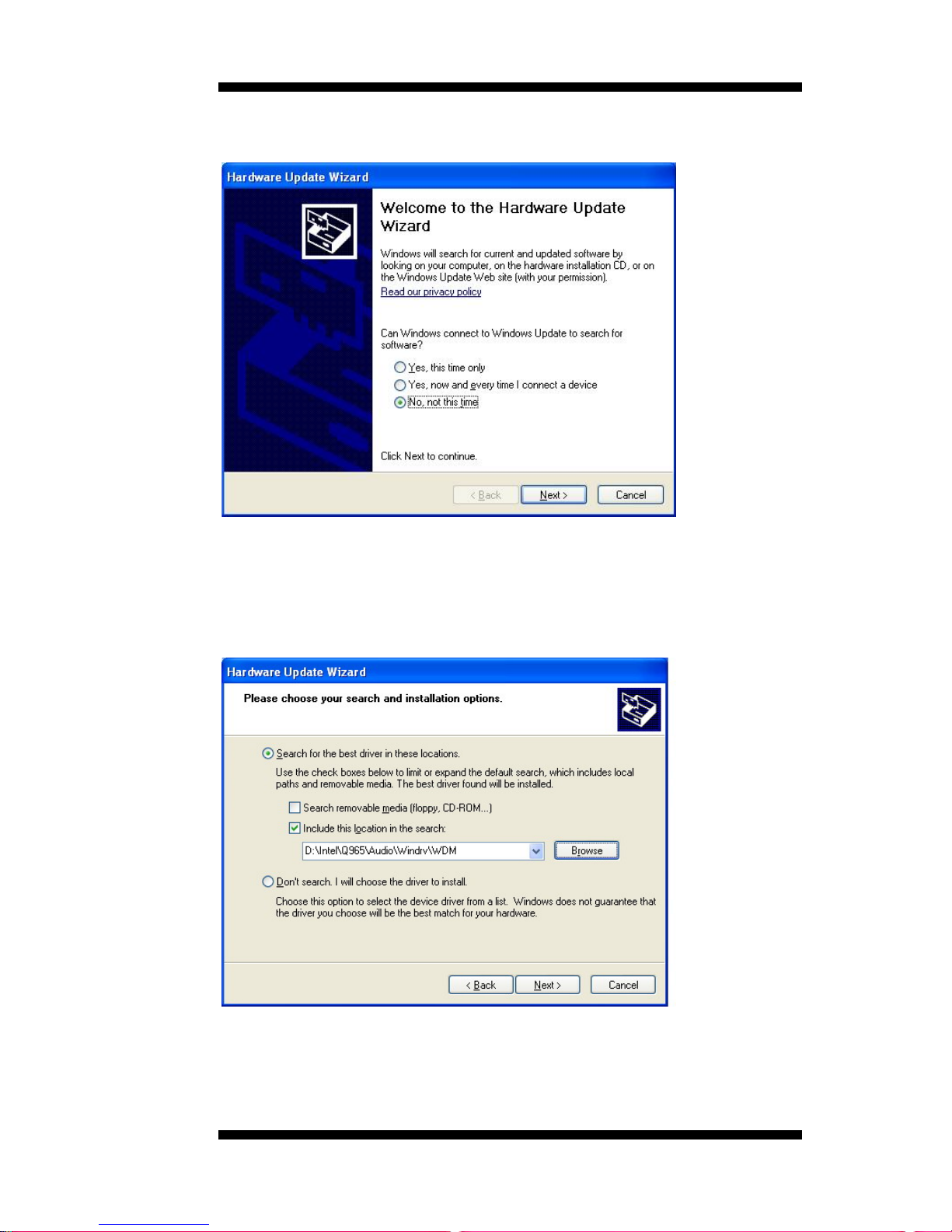
4. When the welcome screen of the Hardware Update Wizard appears,
click No, not this time, and Next to continue.
MI930 User’s Manual 43

DRIVER INSTALLATION
5. On the next screen, select Install from a list or specific location
(Advanced), and click Next to continue.
6. Select Search for the best driver in these locations., and enter the
path where the drivers are located. If E:\ is your CD ROM drive, enter
E:\Ali\AMD690T\SMBUS or click Browse to search for the path.
7. When driver installation is complete, click Finish for changes to take
effect.
44
MI930 User’s Manual

DRIVERS INSTALLATION
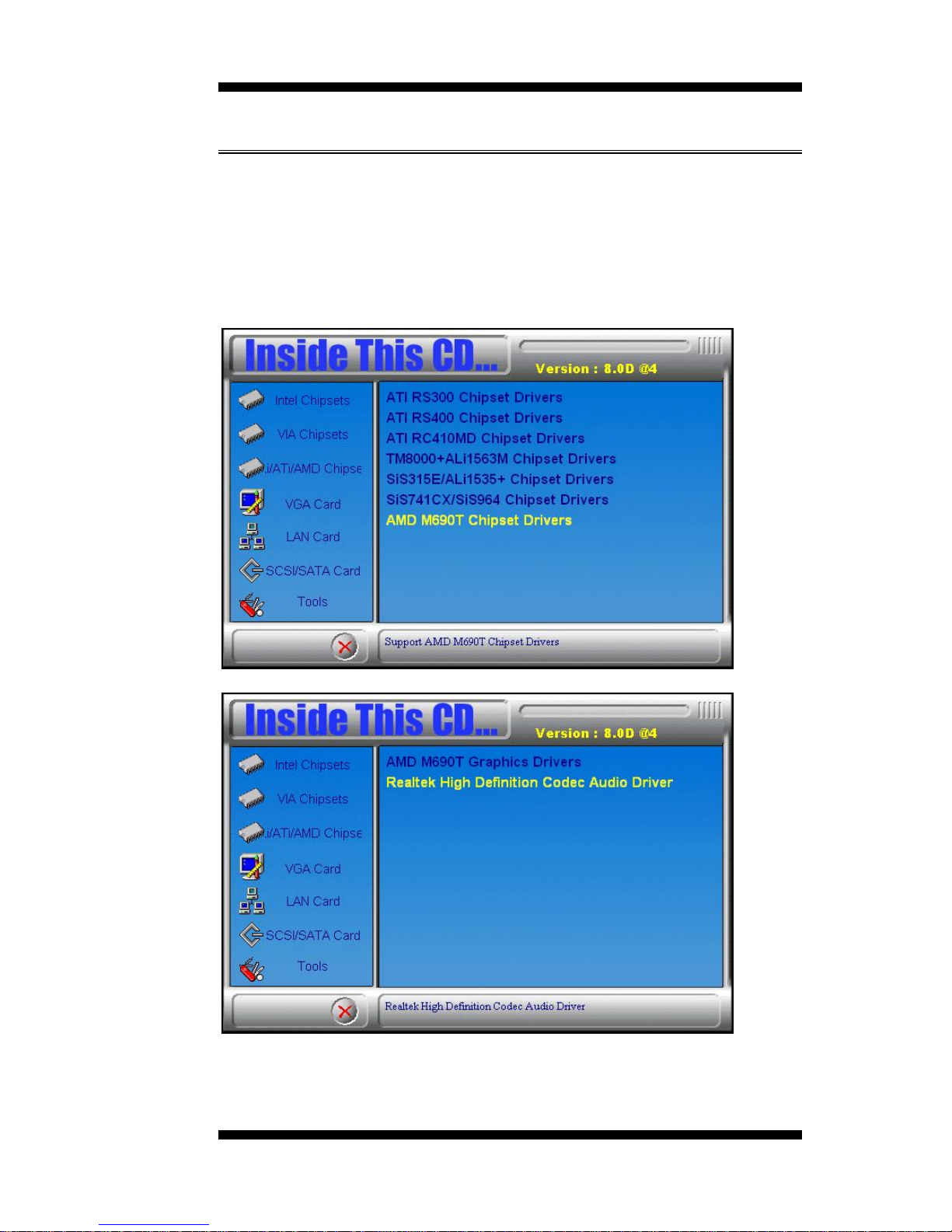
VGA Drivers Installation
To install the VGA drivers, follow the steps below to proceed with the
installation.
1. Insert the CD that comes with the motherboard. Click AMD M690T
Chipset Drivers.
2. Click ATI Radeon X1200 Serial Graphics Drivers as shown below.
Remarks: Before installing this driver, you have to install Microsoft
NET Framework 2.0. Please go the Microsoft website to do this.
MI930 User’s Manual 45

DRIVER INSTALLATION
3. In the Welcome screen, click Next to continue. Then, in the License
Agreement screen, also click Next to continue.
4. When the Select Components screen appears, click Express:
Recommended, in selecting the component thatbyou want to install.
5. When the message regarding Windows Logo testing appears, click
Continue Anyway to proceed with the driver installation.
5. Setup is now complete. Click Finish to restart the computer and for
changes to take effect.
46
MI930 User’s Manual
DRIVERS INSTALLATION
Realtek Codec Audio Driver Installation
Follow the steps below to install the Audio Drivers.
1. Insert the CD that comes with the motherboard. Click AMD M690T
Chipset Drivers. Then, select Realtek High Definition Codect Audio
Driver.
2. Click Realtek AC'97 Codec Audio Driver.
MI930 User’s Manual 47

DRIVER INSTALLATION
3. In the Welcome screen, click Next to continue. After the driver
installation, click Finish on the next screen to restart the computer.
4. In the Windows operating system, go the the Device Manager
window and click on PCI Device with the interjection mark as shown
below.
5. One in the PCI Device Properties window, click on the Driver tab,
and click Update Driver
48
MI930 User’s Manual
DRIVERS INSTALLATION
6. In the Hardware Update Wizard, select No, not this time, and click
Next.
7. In the next screen, the wizard will help you install software for ‘PCI
Device’. Select Install from a list or specific location (Advanced)
and , and click Next to continue. In the next screen (below), enter the
location (if D drive is the source drive for the driver CD) as
D:\Intel\Q965\Audio\Windrv\WDM and click Next to start installing.
8. The Hardware Update Wizard Update is now completed. Click
Finish to restart the computer and for changes to take effect.
MI930 User’s Manual 49
DRIVER INSTALLATION
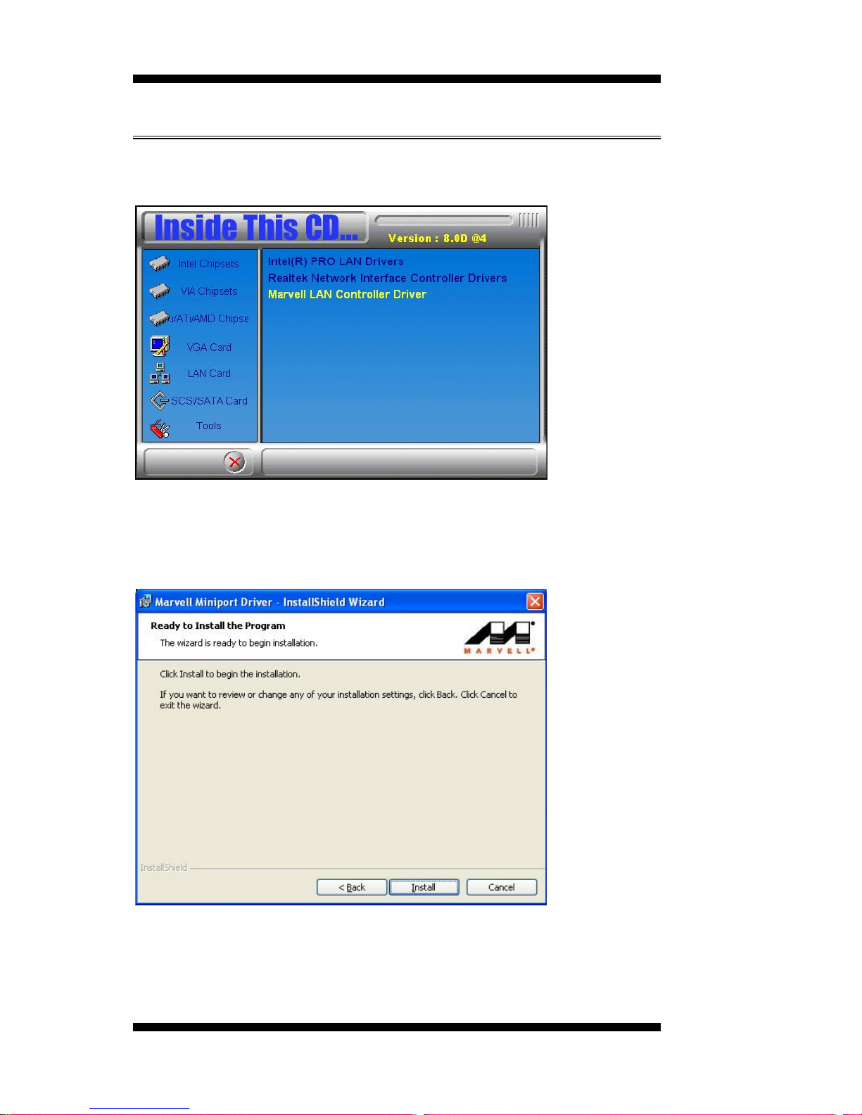
LAN Drivers Installation
1. Insert the CD that comes with the motherboard. Click LAN Card on
the left side and click Marvell LAN Controller Driver.
2. When the Welcome screen of the Marvell Mini port Driver –
InstallShield Wizard appears, click Next to continue. Then, in the next
screen, choose I accept the terms of the license agreement and click
Next to continue. Now, click Install to start begin the installation.
3. Installation is now complete, click Finish to exit the InstallShield
Wizard.
50
MI930 User’s Manual

APPENDIX
MI930 User’s Manual 51
Appendix
A. I/O Port Address Map
Each peripheral device in the system is assigned a set of I/O port
addresses which also becomes the identity of the device. The follo wing
table lists the I/O port addresses used.
Address Device Description
000h - 01Fh DMA Controller #1
020h - 03Fh Interrupt Controller #1
040h - 05Fh Timer
060h - 06Fh Keyboard Controller
070h - 07Fh Real Time Clock, NMI
080h - 09Fh DMA Page Register
0A0h - 0BFh Interrupt Controller #2
0C0h - 0DFh DMA Controller #2
0F0h Clear Math Coprocessor Busy Signal
0F1h Reset Math Coprocessor
1F0h - 1F7h IDE Interface
278 - 27F Parallel Port #2(LPT2)
2F8h - 2FFh Serial Port #2(COM2)
2B0 - 2DF Graphics adapter Controller
378h - 3FFh Parallel Port #1(LPT1)
360 - 36F Network Ports
3B0 - 3BF Monochrome & Printer adapter
3C0 - 3CF EGA adapter
3D0 - 3DF CGA adapter
3F0h - 3F7h Floppy Disk Controller
3F8h - 3FFh Serial Port #1(COM1)

APPENDIX
52
MI930 User’s Manual
B. Interrupt Request Lines (IRQ)
Peripheral devices use interrupt request lines to notify CPU for the
service required. The following tabl e shows the IRQ used by the devices
on board.
Level Function
IRQ0 System Timer Output
IRQ1 Keyboard
IRQ2 Interrupt Cascade
IRQ3 Serial Port #2
IRQ4 Serial Port #1
IRQ5 Reserved
IRQ6 Floppy Disk Controller
IRQ7 Parallel Port #1
IRQ8 Real Time Clock
IRQ9 Reserved
IRQ10 Reserved
IRQ11 Reserved
IRQ12 PS/2 Mouse
IRQ13 80287
IRQ14 Primary IDE
IRQ15 Secondary IDE

APPENDIX
MI930 User’s Manual 53
C. Watchdog Timer Configuration
The WDT is used to generate a variety of output signals after a user
programmable count. The WDT is suitable for use in the prevention of
system lock-up, such as when software becomes trapped in a deadlock.
Under these sorts of circumstances, the timer will count to zero and the
selected outputs will be driven. Under normal circumstance, the user
will restart the WDT at regular intervals before the timer counts to zero.
SAMPLE CODE:
//===========================================================================
//
// THIS CODE AND INFORMATION IS PROVIDED "AS IS" WITHOUT WARRANTY OF ANY
// KIND, EITHER EXPRESSED OR IMPLIED, INCLUDING BUT NOT LIMITED TO THE
// IMPLIED WARRANTIES OF MERCHANTABILITY AND/OR FITNESS FOR A PARTICULAR
// PURPOSE.
//
//===========================================================================
#include <stdio.h>
#include <stdlib.h>
#include "W627EHF.H"
//===========================================================================
int main (int argc, char *argv[]);
void copyright(void);
void EnableWDT(int);
void DisableWDT(void);
//===========================================================================
int main (int argc, char *argv[])
{
unsigned char bBuf;
unsigned char bTime;
char **endptr;
copyright();
if (argc != 2)
{
printf(" Parameter incorrect!!\n");
return 1;
}
if (Init_W627EHF() == 0)
{
printf(" Winbond 83627HF is not detected, program abort.\n");
return 1;
}
bTime = strtol (argv[1], endptr, 10);
printf("System will reset after %d seconds\n", bTime);
EnableWDT(bTime);
return 0;
}
//===========================================================================

APPENDIX
54
MI930 User’s Manual
void copyright(void)
{
printf("\n======== Winbond 83627EHF Watch Timer Tester (AUTO DETECT) ========\n"\
" Usage : W627E_WD reset_time\n"\
" Ex : W627E_WD 3 => reset system after 3 second\n"\
" W627E_WD 0 => disable watch dog timer\n");
}
//===========================================================================
void EnableWDT(int interval)
{
unsigned char bBuf;
bBuf = Get_W627EHF_Reg( 0x2D);
bBuf &= (!0x01);
Set_W627EHF_Reg( 0x2D, bBuf); //Enable WDTO
Set_W627EHF_LD( 0x08); //switch to logic device 8
Set_W627EHF_Reg( 0x30, 0x01); //enable timer
bBuf = Get_W627EHF_Reg( 0xF5);
bBuf &= (!0x08);
Set_W627EHF_Reg( 0xF5, bBuf); //count mode is second
Set_W627EHF_Reg( 0xF6, interval); //set timer
}
//===========================================================================
void DisableWDT(void)
{
Set_W627EHF_LD(0x08); //switch to logic device 8
Set_W627EHF_Reg(0xF6, 0x00); //clear watchdog timer
Set_W627EHF_Reg(0x30, 0x00); //watchdog disabled
}
//===========================================================================

APPENDIX
MI930 User’s Manual 55
//===========================================================================
//
// THIS CODE AND INFORMATION IS PROVIDED "AS IS" WITHOUT WARRANTY OF ANY
// KIND, EITHER EXPRESSED OR IMPLIED, INCLUDING BUT NOT LIMITED TO THE
// IMPLIED WARRANTIES OF MERCHANTABILITY AND/OR FITNESS FOR A PARTICULAR
// PURPOSE.
//
//===========================================================================
#include "W627EHF.H"
#include <dos.h>
//===========================================================================
unsigned int W627EHF_BASE;
void Unlock_W627EHF (void);
void Lock_W627EHF (void);
//===========================================================================
unsigned int Init_W627EHF(void)
{
unsigned int result;
unsigned char ucDid;
W627EHF_BASE = 0x2E;
result = W627EHF_BASE;
ucDid = Get_W627EHF_Reg(0x20);
if (ucDid == 0x88)
{ goto Init_Finish; }
W627EHF_BASE = 0x4E;
result = W627EHF_BASE;
ucDid = Get_W627EHF_Reg(0x20);
if (ucDid == 0x88)
{ goto Init_Finish; }
W627EHF_BASE = 0x00;
result = W627EHF_BASE;
Init_Finish:
return (result);
}
//===========================================================================
void Unlock_W627EHF (void)
{
outportb(W627EHF_INDEX_PORT, W627EHF_UNLOCK);
outportb(W627EHF_INDEX_PORT, W627EHF_UNLOCK);
}
//===========================================================================
void Lock_W627EHF (void)
{
outportb(W627EHF_INDEX_PORT, W627EHF_LOCK);
}
//===========================================================================
void Set_W627EHF_LD( unsigned char LD)
{
Unlock_W627EHF();
outportb(W627EHF_INDEX_PORT, W627EHF_REG_LD);
outportb(W627EHF_DATA_PORT, LD);
Lock_W627EHF();
}

APPENDIX
56
MI930 User’s Manual
//===========================================================================
void Set_W627EHF_Reg( unsigned char REG, unsigned char DATA)
{
Unlock_W627EHF();
outportb(W627EHF_INDEX_PORT, REG);
outportb(W627EHF_DATA_PORT, DATA);
Lock_W627EHF();
}
//===========================================================================
unsigned char Get_W627EHF_Reg(unsigned char REG)
{
unsigned char Result;
Unlock_W627EHF();
outportb(W627EHF_INDEX_PORT, REG);
Result = inportb(W627EHF_DATA_PORT);
Lock_W627EHF();
return Result;
}
//===========================================================================
//===========================================================================
//
// THIS CODE AND INFORMATION IS PROVIDED "AS IS" WITHOUT WARRANTY OF ANY
// KIND, EITHER EXPRESSED OR IMPLIED, INCLUDING BUT NOT LIMITED TO THE
// IMPLIED WARRANTIES OF MERCHANTABILITY AND/OR FITNESS FOR A PARTICULAR
// PURPOSE.
//
//===========================================================================
#ifndef __W627EHF_H
#define __W627EHF_H 1
//===========================================================================
#define W627EHF_INDEX_PORT (W627EHF_BASE)
#define W627EHF_DATA_PORT (W627EHF_BASE+1)
//===========================================================================
#define W627EHF_REG_LD 0x07
//===========================================================================
#define W627EHF_UNLOCK 0x87
#define W627EHF_LOCK 0xAA
//===========================================================================
unsigned int Init_W627EHF(void);
void Set_W627EHF_LD( unsigned char);
void Set_W627EHF_Reg( unsigned char, unsigned char);
unsigned char Get_W627EHF_Reg( unsigned char);
//===========================================================================
#endif //__W627EHF_H
 Loading...