


FWA8506
1U Rackmount
Enterprise Network Appliance
User’s Manual
Version 1.0
(Dec. 2017)

ii
FWA8506 User Manual
Copyright
© 2017 IBASE Technology, Inc. All rights reserved.
No part of this publication may be reproduced, copied, stored in a retrieval system, translated
into any language or transmitted in any form or by any means, electronic, mechanical,
photocopying, or otherwise, without the prior written consent of IBASE Technology, Inc.
(hereinafter referred to as “IBASE”).
Disclaimer
IBASE reserves the right to make changes and improvements to the products described in
this document without prior notice. Every effort has been made to ensure the information in
the document is correct; however, IBASE does not guarantee this document is error-free.
IBASE assumes no liability for incidental or consequential damages arising from
misapplication or inability to use the product or the information contained herein, nor for any
infringements of rights of third parties, which may result from its use.
Trademarks
All the trademarks, registrations and brands mentioned herein are used for identification
purposes only and may be trademarks and/or registered trademarks of their respective
owners.

FWA8506 User Manual
iii
Compliance
The product described in this manual complies with all applicable European Union
(CE) directives if it has a CE marking. For systems to remain CE compliant, only CEcompliant parts may be used. Maintaining CE compliance also requires proper cable
and cabling techniques.
This product has been tested and found to comply with the limits for a Class A
device, pursuant to Part 15 of the FCC Rules. These limits are designed to provide
reasonable protection against harmful interference in a residential installation. This
equipment generates, uses and can radiate radio frequency energy and, if not
installed and used in accordance with manufacturer’s instructions, may cause
harmful interference to radio communications.
WEEE
This product must not be disposed of as normal household waste, in
accordance with the EU directive of for waste electrical and electronic
equipment (WEEE - 2012/19/EU). Instead, it should be disposed of by
returning it to a municipal recycling collection point. Check local
regulations for disposal of electronic products.
Green IBASE
This product complies with the current RoHS directives restricting the
use of the following substances in concentrations not to exceed 0.1%
by weight (1000 ppm) except for cadmium, limited to 0.01% by weight
(100 ppm).
• Lead (Pb)
• Mercury (Hg)
• Cadmium (Cd)
• Hexavalent chromium (Cr6+)
• Polybrominated biphenyls (PBB)
• Polybrominated diphenyl ether (PBDE)

iv
FWA8506 User Manual
Important Safety Information
Carefully read the following safety information before using the device.
Setting up your system:
• Put the device horizontally on a stable and solid surface.
• Do not use this product near water or any heated source.
• Leave plenty of space around the device and do not block the ventilation
openings. Never drop or insert any objects of any kind into the openings.
• Use this product in environments with ambient temperatures between 0˚C and
40˚C.
Care during use:
• Do not place heavy objects on the top of the device.
• Make sure to connect the correct voltage to the device. Failure to supply the
correct voltage could damage the unit.
• Do not walk on the power cord or allow anything to rest on it.
• If you use an extension cord, make sure the total ampere rating of all devices
plugged into the extension cord does not cord’s ampere rating.
• Do not spill water or any other liquids on your device.
• Always unplug the power cord from the wall outlet before cleaning the device.
• Only use neutral cleaning agents to clean the device.
• Vacuum dust and particles from the vents by using a computer vacuum cleaner.
Product Disassembly
Do not try to repair, disassemble, or make modifications to the device. Doing so will
void the warranty and may result in damage to the product or personal injury.
CAUTION
There is a danger of explosion if the lithium-ion battery is replaced with an incorrect
battery. Replace only with the same or equivalent type recommended by the
manufacturer. Dispose of used batteries by observing local regulations.

FWA8506 User Manual
v
Warranty Policy
• IBASE standard products:
24-month (2-year) warranty from the date of shipment. If the date of shipment
cannot be ascertained, the product serial numbers can be used to determine
the approximate shipping date.
• 3rd-party parts:
12-month (1-year) warranty from delivery for the 3rd-party parts that are not
manufactured by IBASE, such as CPU, memory, HDD, power adapter, panel
and touchscreen.
* PRODUCTS, HOWEVER, THAT FAILS DUE TO MISUSE, ACCIDENT,
IMPROPER INSTALLATION OR UNAUTHORIZED REPAIR SHALL BE
TREATED AS OUT OF WARRANTY AND CUSTOMERS SHALL BE BILLED
FOR REPAIR AND SHIPPING CHARGES.
Technical Support & Services
1. Visit the IBASE website at www.ibase.com.tw to find the latest information about
the product.
2. If you encounter any technical problems and require assistance from your
distributor or sales representative, please prepare and send the following
information:
• Product model name
• Product serial number
• Detailed description of the problem
• The error messages in text or in screenshots if there is any
• The arrangement of the peripherals
• Software in use (such as OS and application software, including the version
numbers)
3. If repair service is required, you can download the RMA form at
http://www.ibase.com.tw/english/Supports/RMAService/. Fill out the form and
contact your distributor or sales representative.

vi
FWA8506 User Manual
Table of Contents
Compliance.................................................................................................... iii
Important Safety Information ....................................................................... iv
CAUTION ....................................................................................................... iv
Warranty Policy .............................................................................................. v
Technical Support & Services ...................................................................... v
Chapter 1 General Information ................................................................ 1
1.1 Introduction ............................................................................................. 2
1.2 Features .................................................................................................. 3
1.3 Packing List ............................................................................................ 3
1.4 Optional Accessories .............................................................................. 3
1.5 Specifications .......................................................................................... 4
1.6 Overview ................................................................................................. 6
1.7 Dimensions ............................................................................................. 8
Chapter 2 Hardware Configuration ......................................................... 9
2.1 Installations ........................................................................................... 10
2.1.1 Memory Installation / Replacement ......................................... 11
2.1.2 HDD Installation / Replacement .............................................. 12
2.1.3 CF Card Installation / Replacement ........................................ 13
2.1.4 Fan Module Installation / Replacement ................................... 14
2.2 Setting the Jumpers .............................................................................. 15
2.2.1 How to Set Jumpers ............................................................... 15
2.3 Jumper & Connector Locations on Motherboard ................................... 16
2.4 Jumpers Quick Reference ..................................................................... 17
2.4.1 CPU SV Mode Selection (JP2) ............................................... 17
2.4.2 Clear CMOS Data (JP3) ......................................................... 18
2.4.3 Clear RTC Data (JP5) ............................................................. 19
2.4.4 AT & ATX Mode Selection (JP6) ............................................. 20
2.5 Connectors Quick Reference ................................................................ 21
2.5.1 COM2 Port (CN3) ................................................................... 22
2.5.2 PM Bus Connector (J14) ........................................................ 22
2.5.3 SATA Power Connector (J7, J10) ........................................... 23
2.5.4 System Function Connector (JP8) .......................................... 23

FWA8506 User Manual
vii
2.5.5 Digital I/O Port (JP10) ............................................................. 25
2.5.6 Fan Power Connector (CPU_FAN1, SYS_FAN1, SYS_FAN2) .. 25
Chapter 3 BIOS Setup ............................................................................ 26
3.1 Introduction ........................................................................................... 27
3.2 BIOS Setup ........................................................................................... 27
3.3 Main Settings ........................................................................................ 28
3.4 Advanced Settings ................................................................................ 29
3.4.1 Trusted Computing ................................................................. 30
3.4.2 PCIE Link Configuration ......................................................... 31
3.4.3 NCT5523D Super IO Configuration ........................................ 32
3.4.4 Hardware Monitor ................................................................... 35
3.4.5 LAN Bypass Configuration ...................................................... 36
3.4.6 Serial Port Console Redirection .............................................. 37
3.4.7 Console Port Redirection Settings .......................................... 38
3.4.8 USB Configuration .................................................................. 39
3.4.9 CSM Configuration ................................................................ . 40
3.5 Intel RC Setup ....................................................................................... 41
3.5.1 Processor Configuration ......................................................... 42
3.5.2 System Event Log .................................................................. 43
3.5.3 South Bridge Chipset Configuration ........................................ 47
3.6 Security Settings ................................................................................... 49
3.7 Boot Settings......................................................................................... 50
3.8 Save & Exit Settings.............................................................................. 51
Appendix ...................................................................................................... 52
A. I/O Port Address Map ............................................................................ 53
B. Interrupt Request Lines (IRQ) ............................................................... 56
C. Watchdog Timer Configuration .............................................................. 58

1
Chapter 1
General Information
The information provided in this chapter includes:
• Features
• Packing List
• Optional Accessories
• Specifications
• Overview
• Dimensions

2
FWA8506 User Manual
1.1 Introduction
FWA8506 series is specifically designed for the network security and
management market. There are plenty of applications adopting network
security or network management as listed below.
Network Security Applications:
• Firewall
• Unified Threat Management (UTM)
• Virtual Private Network (VPN)
• Proxy Server
• Caching Server
Network Management Applications:
• Load balancing
• Quality of Service
• Remote Access Service
Photo of FWA8506

General Information
FWA8506 User Manual
3
1
1.2 Features
• 1U rackmount platform designed with Intel
®
Atom® C3000 processor
• 2 x DDR4 DIMM 2400 MHz, expandable up to 32 GB for UDIMM (ECC /
non-ECC) and up to 64 GB for RDIMM
• 6 x GbE LAN ports with 2 advanced LAN Bypass pairs
• 4 x 10 GbE SFP+ ports
• CF slot and PCIe (x8) expansion slot(s)
1.3 Packing List
Your product package should include the items listed below. If any of the
items below is missing, contact the distributor or the dealer from whom you
purchased the product.
• FWA8506 x 1
• Power Cord x 1
• Rackmount Bracket x 2
1.4 Optional Accessories
IBASE provide optional accessories as follows. Please contact us or your
dealer if you need any.
• Console Cable (160 cm, PK1-51)
• Riser Card (IPN104)

4
FWA8506 User Manual
1.5 Specifications
Product Name
FWA8506
System
Motherboard
MBN802-8C40G
Operating
System
• Windows 10 (64-bit)
• Linux Ubuntu 16.04.3
CPU
Intel® Atom® C3758
Chipset
Integrated
Memory
• 2 x DDR4 UDIMM 400 MHz, expandable to 32 GB
(ECC / non-ECC)
• 2 x DDR4 RDIMM 2400 MHz, expandable to 64 GB
Storage
• Max. 2 x 2.5” HDD or SSD internal drive bay
• On-board CF slot
Network
6 x Intel® I211AT GbE
Bypass
2 x segments (LAN3 / LAN4 & LAN5 / LAN6)
Super I/O
Nuvoton NCT5523D
IPMI
N/A
Power Supply
Full range 250W ATX power supply
BIOS
AMI BIOS
TPM
1.2
Watchdog
Watchdog Timer 256 segments, 0, 1, 2…255 sec/min
Chassis
Steel with textured black color paint
Dimensions
(W x H x D)
438 x 44 x 340 mm (17.24” x 1.73” x 13.38”)
Weight
8 kg (17.64 lb)
Certificate
CE / FCC Class A
Front I/O Ports
Console
1 x Console port
Traffic LAN
Port
6 x RJ45 GbE LAN ports
USB
2 x USB 3.0
Rear I/O Ports
Power Inlet
1 x AC inlet 100V ~ 240V, 47 ~ 63 Hz
CF
1 x CF slot
Fan
3 x system fan module

General Information
FWA8506 User Manual
5
1
Expansion
1 x PCIe (x8) slot (4-lane)
Environment
Temperature
• Operating: 0 ~ 40 °C (32 ~ 104 °F)
• Storage: -20~ 70 °C (-4 ~ 158 °F)
Relative
Humidity
5 ~ 90%
Vibration
Protection
• Operating: 0.25 Grms / 3 ~ 500 Hz (Z-axis)
• Non-operating: 1.0 Grms / 3 ~ 500Hz (Z-axis)
Shock
Protection
Half-sinewave 50G Z-axis
All specifications are subject to change without prior notice.

6
FWA8506 User Manual
1.6 Overview
Front View
No.
Name
No.
Name
1
LCM Display with 4 buttons
5
Reserved Area for HDD/SSD
or expansion card
2
LED Indicators(from top to
bottom: Status, HDD, Power)
6
USB 3.0 Ports
3
Console Port
7
User Self-defined Button
(with GPI Signal)
4
GbE LAN Ports
Oblique View
General Information
FWA8506 User Manual
7
1
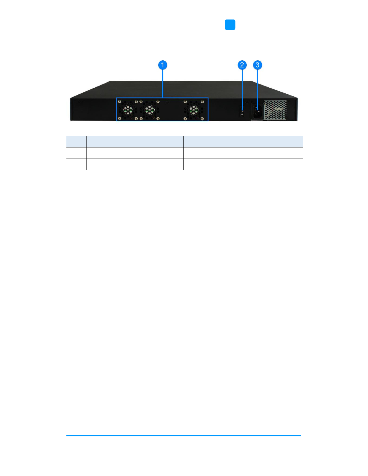
Rear View
No.
Name
No.
Name
1
System Fans
3
AC Power Inlet
2
Power Switch

8
FWA8506 User Manual
1.7 Dimensions
Unit: mm

9
Chapter 2
Hardware Configuration
The information provided in this chapter includes:
• installations
• Information and locations of connectors

10
FWA8506 User Manual
2.1 Installations
For installation or replacement of the memory modules, HDD/SSD, CF card
and fans, you need to disassemble the device cover first by loosening 9
screws as indicated below.
Configuration inside the device:
Area-A shown below can fit optional HDD/SSD and Area-B can fit one or two
optional HDD/SSD or an expansion card .

Hardware Configuration
FWA8506 User Manual
11
2
2.1.1 Memory Installation / Replacement
If you need to install or replace a memory module, follow the instructions
below after you have removed the device cover.
1. Locate the memory slots in the device.
2. Press the ejector tab of the memory slot down and outwards with your
fingertips.
3. Hold the memory module and align the key of the module with that on the
memory slot.
4. Gently push the module in an upright position until the ejector tabs of the
memory slot close to hold the module in place when the module touches
the bottom of the slot.
To remove the module, press the ejector tabs outwards with your fingertips to
eject the module.

12
FWA8506 User Manual
2.1.2 HDD Installation / Replacement
After removing the device cover, notice Optional Area-A for 2.5” HDD/SSD
and Optional Area-B for 2.5” HDD/SSD or expansion as shown below. If you
need to install or replace an HDD/SDD or an expansion card, follow the
instructions below.
1. Remove 4 screws as indicated below for each HDD/SSD (8 screws for two
HDD/SSD).
2. Install a new HDD/SDD onto the tray and fasten the 4 screws for each
HDD/SDD.

Hardware Configuration
FWA8506 User Manual
13
2
3. Secure the tray with HDD from the bottom of the device as ilustrated
below.
2.1.3 CF Card Installation / Replacement
If you need to replace a CF card, remove the device cover firstly, locate the
CF slot and Insert the CF card to the slot.
‘To remove the CF card, pull it out with your thumb and index finger directly.

14
FWA8506 User Manual
2.1.4 Fan Module Installation / Replacement
If you need to replace a fan module, remove the device cover and the
corresponding 4 screws of the fan module on the rear side as shown.
Take out the fan, replace with a new one, and fasten the screws.

Hardware Configuration
FWA8506 User Manual
15
2
2.2 Setting the Jumpers
Set up and configure your device by using jumpers for various settings and
features according to your needs and applications. Contact your supplier if
you have doubts about the best configuration for your use.
2.2.1 How to Set Jumpers
Jumpers are short-length conductors consisting of several metal pins with a
non-conductive base mounted on the circuit board. Jumper caps are used to
have the functions and features enabled or disabled. If a jumper has 3 pins,
you can connect either PIN1 to PIN2 or PIN2 to PIN3 by shorting.
A 3-pin jumper
A jumper cap
Refer to the illustration below to set jumpers.
Pin closed
Oblique view
Jumper Settings
Open
1-2
2-3
When two pins of a jumper are encased in a jumper cap, this jumper is
closed, i.e. turned On.
When a jumper cap is removed from two jumper pins, this jumper is open, i.e.
turned Off.
Pin# 1
2
3
1 2 3
1 2 3
1 2 3

16
FWA8506 User Manual
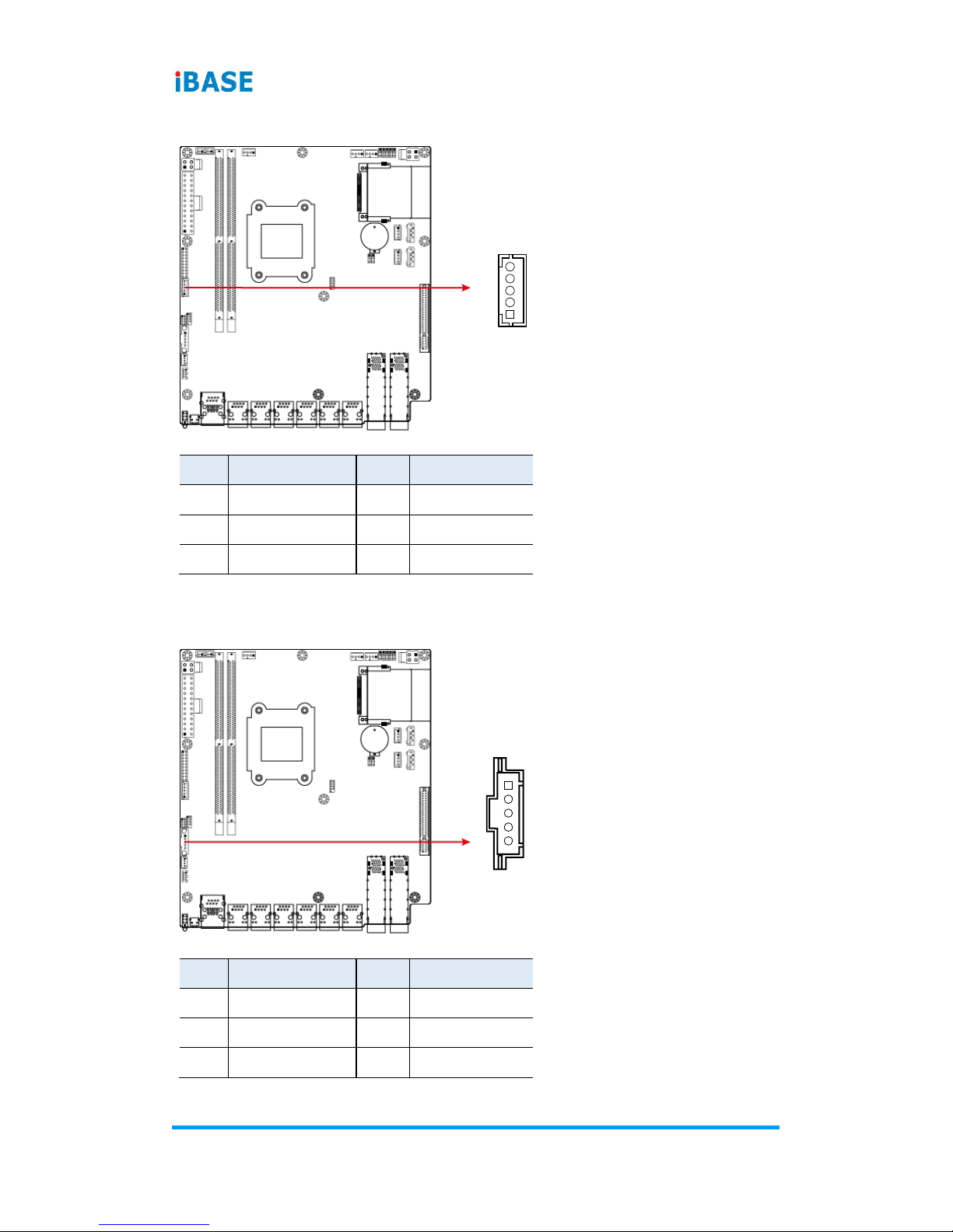
2.3 Jumper & Connector Locations on Motherboard
Motherboard: MBN802

Hardware Configuration
FWA8506 User Manual
17
2
2.4 Jumpers Quick Reference
Function
Connector
Page
CPU SV Mode Selection
JP2
17
Clear CMOS Data
JP3
18
Clear RTC Data
JP5
19
AT & ATX Mode Selection
JP6
20
Factory Use Only
JP4, JP7, JP11
--
2.4.1 CPU SV Mode Selection (JP2)
Function
Pin closed
Setting
CPU SV
1-2
Normal
(default)
2-3
1
1
1

18
FWA8506 User Manual
2.4.2 Clear CMOS Data (JP3)
Function
Pin closed
Setting
Normal
(default)
1-2
Clear CMOS
2-3
1
1
1

Hardware Configuration
FWA8506 User Manual
19
2
2.4.3 Clear RTC Data (JP5)
Function
Pin closed
Setting
Normal
(default)
1-2
Clear RTC
2-3
1
1
1

20
FWA8506 User Manual
2.4.4 AT & ATX Mode Selection (JP6)
Function
Pin closed
Setting
AT
(default)
1-2
ATX
2-3
1
1
1

Hardware Configuration
FWA8506 User Manual
21
2
2.5 Connectors Quick Reference
Function
Connector Name
Page
COM2 Port
CN3
22
PM Bus Connector
J14
22
SATA Power Connector
J7, J10
23
System Function Connector
JP8
23
Digital I/O Port
JP10
25
Fan Power Connector
CPU_FAN1, SYS_FAN1,
SYS_FAN2
25
USB 2.0 Connector
F_USB1
--
AT / ATX Power Switch Connector
J1 (AT), J2 (ATX)
--
ATX 12V Output Connector
J3
--
ATX Power Connector
J4, J6
--
CF Card Slot
J5
--
SATA Port
CN1, CN2
--
GbE RJ45 LAN Port
CN7, CN12
--
10 GbE SFP+ Port
CN4, CN5
--
Console Port & USB 3.0 Ports
CN6
--
User Self-defined Button (with GPI
Signal)
SW1
-PCIe (x8) Connector
PCIE1
--
LED Indicators
LED10
--
Factory Use Only
J11, J13, JP9
--
22
FWA8506 User Manual
2.5.1 COM2 Port (CN3)
Pin
Assignment
Pin
Assignment
1
SIN
4
VCC5
2
SOUT
5
NC
3
Ground
2.5.2 PM Bus Connector (J14)
Pin
Assignment
Pin
Assignment
1
CLK
4
Ground
2
DATA
5
+3.3V
3
NC
1
1

Hardware Configuration
FWA8506 User Manual
23
2
2.5.3 SATA Power Connector (J7, J10)
J7
J10
Pin
Assignment
Pin
Assignment
1
VCC5
3
Ground
2
Ground
4
VCC12
2.5.4 System Function Connector (JP8)
JP8 provides light indicators of the computer activities and status. It provides
interfaces for the following functions:
1
1
19 20
2

24
FWA8506 User Manual
• Power LED (Pins 1, and 5)
This connector connects to the system power LED on control panel. This
LED will light when the system turns on.
Pin
Assignment
Pin
Assignment
1
+5V
5
Ground
• ATX Power ON Switch (Pins 13 and 14)
The 2 pins make an “ATX Power Supply On/Off Switch” for the system
that connects to the power switch on the case. When pressed, the power
switch will force the system to power on. When pressed again, it will
power off the system.
Pin
Assignment
Pin
Assignment
13
Power_ON
14
Ground
• Reset Switch (Pins 17 and 18)
The reset switch allows you to reset the system without turning the main
power switch off and then on again. Orientation is not required when
making a connection to this header.
Pin
Assignment
Pin
Assignment
17
SYSRST#
18
Ground
• Hard Disk Drive LED Connector (Pins 19 and 20)
This connector connects to the hard drive activity LED on control panel.
This LED will flash when the HDD is being accessed.
Pin
Assignment
Pin
Assignment
19
+3.3V
20
-HDD_LED
• Bypass LED1 (Pins 9 and 10)
The two pins make an external LED connector light for LAN bypass.
Pin
Assignment
Pin
Assignment
9
+5V
10
BYPASS0_LED-
• Bypass LED2 (Pins 11 and 12)
The two pins make an external LED connector light for LAN bypass.
Pin
Assignment
Pin
Assignment
11
+5V
12
BYPASS1_LED-

Hardware Configuration
FWA8506 User Manual
25
2
2.5.5 Digital I/O Port (JP10)
Pin
Assignment
Pin
Assignment
1
Ground
2
VCC5
3
IN1
4
OUT1
5
IN2
6
OUT2
7
IN3
8
OUT3
2.5.6 Fan Power Connector (CPU_FAN1, SYS_FAN1, SYS_FAN2)
SYS_FAN1
SYS_FAN2
CPU_FAN1
Pin
Assignment
Pin
Assignment
1
Ground
3
Rotation detection
2
+12V
4
Rotation control
8
7
1
2
1

26
Chapter 3
BIOS Setup
This chapter describes the different settings available in the AMI
BIOS that comes with the board. The topics covered in this chapter
are as follows:
• Main Settings
• Advanced Settings
• Chipset Settings
• Security Settings
• Book Settings
• Save & Exit

BIOS Setup
FWA8506 User Manual
27
4
3.1 Introduction
The BIOS (Basic Input/Output System) installed in the ROM of your computer
system supports Intel® processors. The BIOS provides critical low-level
support for standard devices such as disk drives, serial ports and parallel
ports. It also provides password protection as well as special support for
detailed fine-tuning of the chipset controlling the entire system.
3.2 BIOS Setup
The BIOS provides a Setup utility program for specifying the system
configurations and settings. The BIOS ROM of the system stores the Setup
utility. When you turn on the computer, the BIOS is immediately activated.
Press the <Del> key immediately allows you to enter the Setup utility. If you
are a little bit late pressing the <Del> key, POST (Power On Self Test) will
continue with its test routines, thus preventing you from invoking the Setup.
If you still need to enter Setup, restart the system by pressing the ”Reset”
button or simultaneously pressing the <Ctrl>, <Alt> and <Delete> keys.
You can also restart by turning the system Off and back On again.
The following message will appear on the screen:
Press <DEL> to Enter Setup
In general, press the arrow keys to highlight items, <Enter> to select, the
<PgUp> and <PgDn> keys to change entries, <F1> for help, and <Esc> to
quit.
When you enter the BIOS Setup utility, the Main Menu screen will appear on
the screen. The Main Menu allows you to select from various setup functions
and exit choices.
Warning: It is strongly recommended that you avoid making any changes to
the chipset defaults.
These defaults have been carefully chosen by both AMI and your
system manufacturer to provide the absolute maximum
performance and reliability. Changing the defaults could make the
system unstable and crash in some cases.

28
FWA8506 User Manual
3.3 Main Settings
BIOS Setting
Description
System Date
Sets the date.
Use the <Tab> key to switch between the data
elements.
System Time
Set the time.
Use the <Tab> key to switch between the data
elements.

BIOS Setup
FWA8506 User Manual
29
4
3.4 Advanced Settings
This section allows you to configure, improve your system and allows you to
set up some system features according to your preference.

30
FWA8506 User Manual
3.4.1 Trusted Computing
BIOS Setting
Description
Security Device
Support
Enables / Disables TPM support. O.S. will not show
TPM. Reset of platform is required.
TPM State
Enables / Disables the security device.
Note: Your computer will reboot during restart in
order to change state of the device.
Pending operation
Schedule an operation for the security device.
Note: Your computer will reboot during restart in
order to change the state of security device.

BIOS Setup
FWA8506 User Manual
31
4
3.4.2 PCIE Link Configuration
BIOS Setting
Description
PCIE x4 Link Speed
Select upper limit on link operational speed for PCI
Express RootPort.
Options: Auto, Gen1, Gen2, Gen3

32
FWA8506 User Manual
3.4.3 NCT5523D Super IO Configuration
BIOS Setting
Description
Serial Port
Configuration
Sets Parameters of Serial Ports.
You can enable / disable the serial port and select
an optimal settings for the Super IO device.

BIOS Setup
FWA8506 User Manual
33
4
3.4.3.1. Serial Port 1 Configuration
BIOS Setting
Description
Serial Port
Enables / Disables serial port (COM).
Change Settings
Selects an optimal settings for the Super I/O device.
Options:
• Auto
• IO=3F8h ; IRQ=4
• IO=3F8h ; IRQ=3, 4, 5, 6, 7, 9. 10, 11, 12
• IO=2F8h ; IRQ=3, 4, 5, 6, 7, 9. 10, 11, 12
• IO=3E8h ; IRQ=3, 4, 5, 6, 7, 9. 10, 11, 12
• IO=2E8h ; IRQ=3, 4, 5, 6, 7, 9. 10, 11, 12

34
FWA8506 User Manual
3.4.3.2. Serial Port 2 Configuration
BIOS Setting
Description
Serial Port
Enables / Disables serial port (COM).
Change Settings
Selects an optimal settings for the Super I/O device.
Options:
• Auto
• IO=2F8h ; IRQ=3
• IO=3F8h ; IRQ=3, 4, 5, 6, 7, 9. 10, 11, 12
• IO=2F8h ; IRQ=3, 4, 5, 6, 7, 9. 10, 11, 12
• IO=3E8h ; IRQ=3, 4, 5, 6, 7, 9. 10, 11, 12
• IO=2E8h ; IRQ=3, 4, 5, 6, 7, 9. 10, 11, 12

BIOS Setup
FWA8506 User Manual
35
4
3.4.4 Hardware Monitor
BIOS Setting
Description
Power Failure
Selects S0/S5 for ACPI state after a G3.
Options: Power On, Power Off, Last State
ACPI Shutdown
Temperature
This field enables or disables the Shutdown
Temperature
Options: Disabled,. 70°C, 75°C, 80°C, 85°C,
90°C, 95°C
CPU Smart Fan
Control
Sets up or disable the fan control for start-up
temperature.
Options: Disabled, 40°C, 45°C, 50°C, 55°C,
60°C, 65°C, 70°C
Temperatures /
Voltages
These fields are the parameters of the hardware
monitoring function feature of the motherboard. The
values are read-only as monitored by the system
and showing the PC health status
36
FWA8506 User Manual
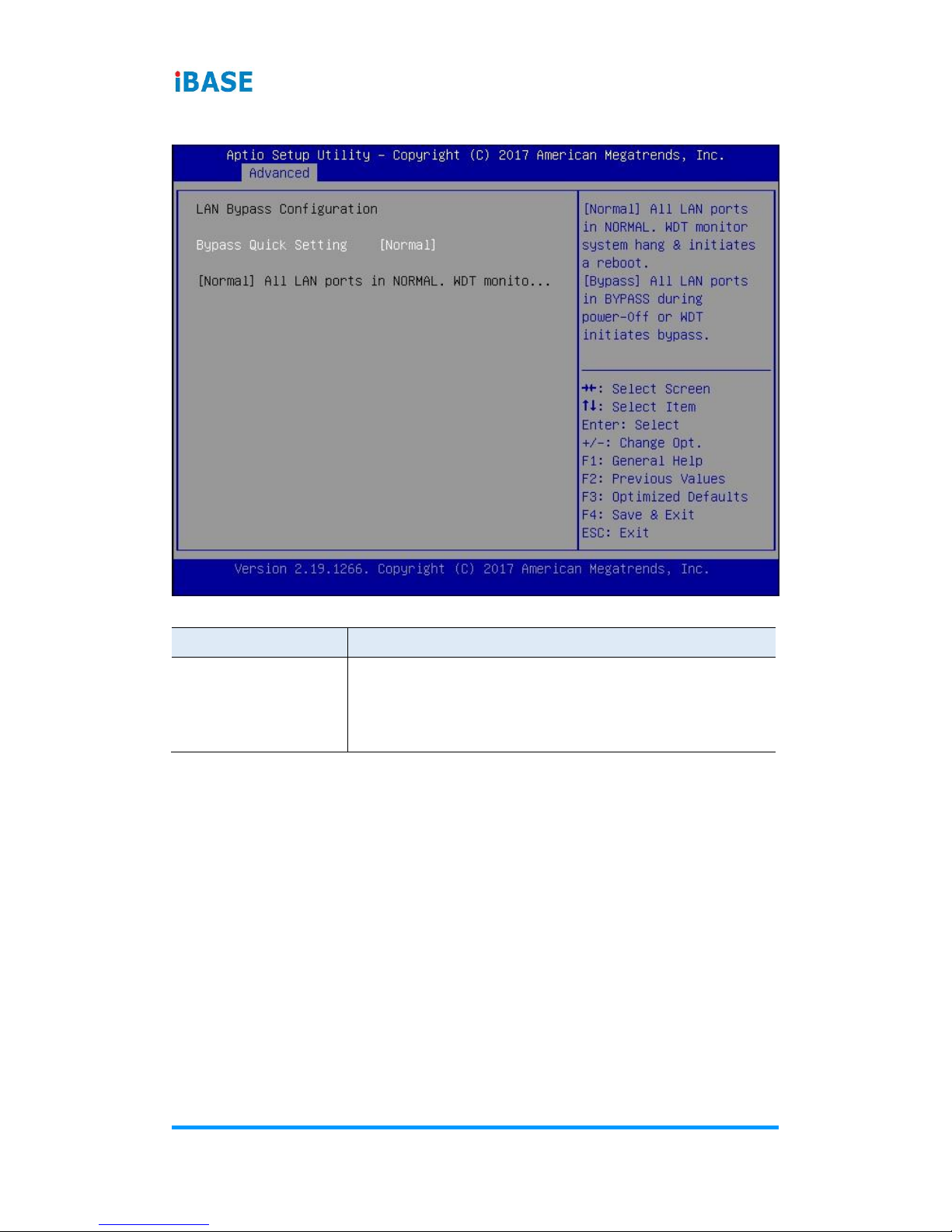
3.4.5 LAN Bypass Configuration
BIOS Setting
Description
Bypass Quick
Setting
Normal: All LAN ports in Normal state. WDT mointor
system hang & initiates a reboot.
Bypass: All LAN ports in BYPASS during power-off
or WDT initiates bypass.
BIOS Setup
FWA8506 User Manual
37
4
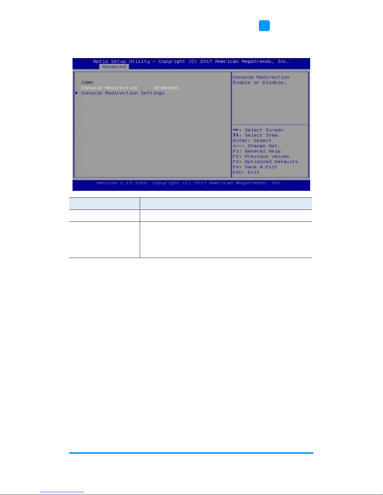
3.4.6 Serial Port Console Redirection
BIOS Setting
Description
Console Redirection
Enables / Disables the Console Redirection.
Console Recirection
Settings
The settings specify how the host computer and the
remote computer (which the user is using) will
exchange data. Both computers should have the
same or compatible settings.

38
FWA8506 User Manual
3.4.7 Console Port Redirection Settings
BIOS Setting
Description
Terminal Type
Emulation: ANSI: Extended ASCII char set.
VT100: ASCII char set.
VT100+: Extends VT100 to support color, function
keys, etc.
VT-UTF8: Uses UTF8 encoding to map Unicode
Options: VT100, VT100+, VT-UTF8, ANSI
Bits per second
Selects serial port transmission speed. The speed
must be matched on the other side. Long or noisy
lines may require lower speeds.
Options: 9600, 19200, 38400, 57600, 115200
Data Bits
Selects the data bits as 7 or 8.
Parity
A parity bit can be sent with the data bits to detect
some transmission errors.
Options: None, Even, Odd, Mark, Space
Stop Bits
Stop bits indicates the end of a serial data packet. (A
start bit indicates the beginning). The standard
setting is 1 stop bit.
Options: 1, 2
Flow Control
Flow control can prevent data loss from buffer
overflow. When sending data, if the receiving buffers
are full, a “stop” signal can be sent to stop the data
flow.
Options: None, Hardware RTS/CTS

BIOS Setup
FWA8506 User Manual
39
4
BIOS Setting
Description
VT-UTF8 Combo
Key support
Enables / Disables VT-UTF8 combination key
support for ANSI/VT100 terminals.
Recorder Mode
With this mode enabled only text will be sent. This is
to capture terminal data.
Resolution 100 x 31
Enables / Disables extended terminal resolution.
Putty KeyPad
Selects FunctionKey and KeyPad on Putty.
3.4.8 USB Configuration
BIOS Setting
Description
Legacy USB Support
Enables / Disables Legacy USB support.
• Auto disables legacy support if there is no USB
device connected.
• Disable keeps USB devices available only for
EFI applications.

40
FWA8506 User Manual
3.4.9 CSM Configuration
BIOS Setting
Description
Boot option filter
Controls Legacy/UEFI ROMs priority.
Options: UEFI and Legacy, Legacy only, UEFI only
Network
Controls the execution of UEFI and Legacy PXE
OpROM.
Options: Do not launch, Legacy

BIOS Setup
FWA8506 User Manual
41
4
3.5 Intel RC Setup

42
FWA8506 User Manual
3.5.1 Processor Configuration
BIOS Setting
Description
EIST (GV3)
Enables / Disables EIST. GV3 and TM1 must be
enabled for TM2 to be available. GV3 msut be
available for Turbo.
Turbo
Enables / Disables CPU Turbo capability. This option
only applies to EC2 and above.
VT-d
Enables / Disables VT-d.
VT-x
Enables / Disables VT-x.
BIOS Setup
FWA8506 User Manual
43
4
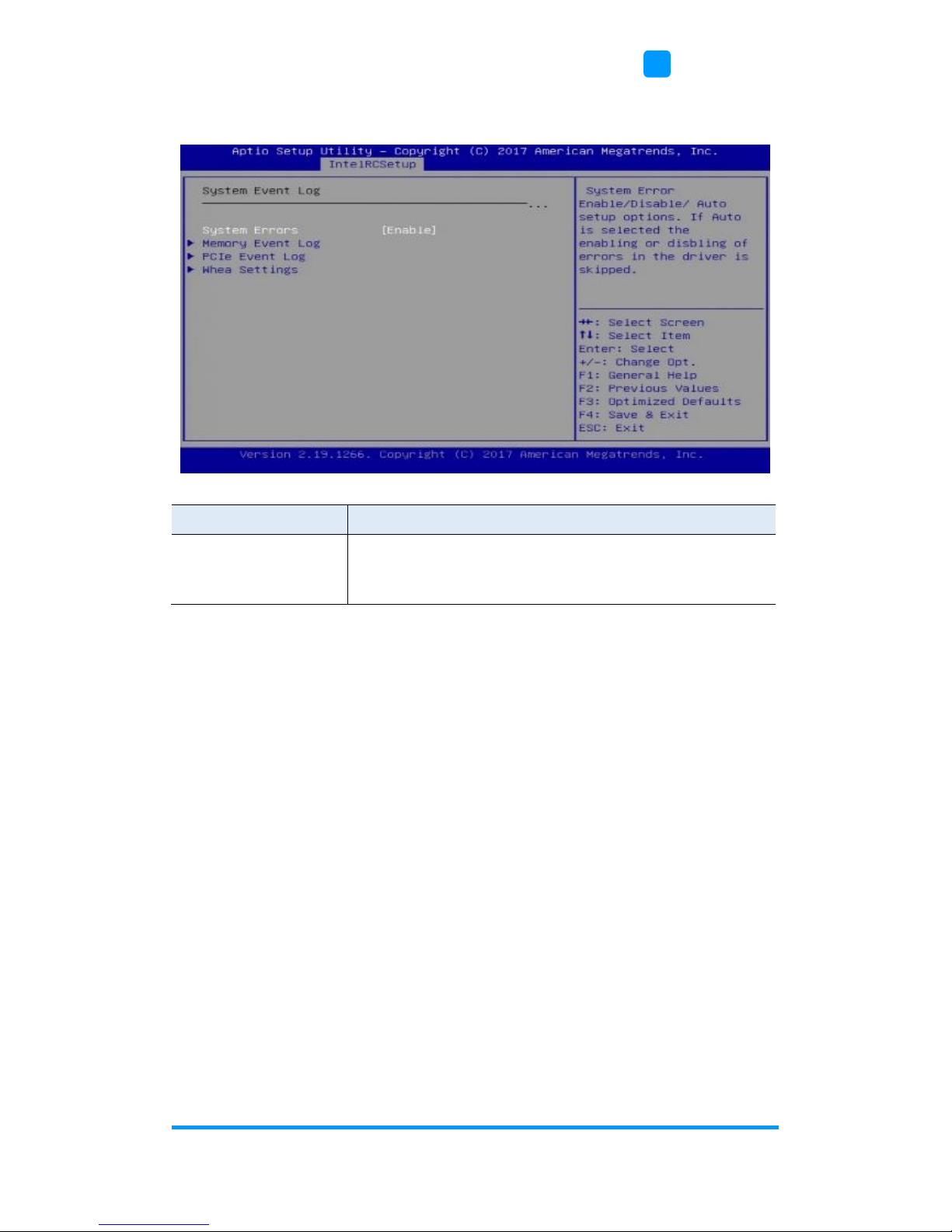
3.5.2 System Event Log
BIOS Setting
Description
System Errors
Enables / Disables / Automatically sets up options. If
Auto is selected, the enabling or disabling of errorsin
the driver is skipped.

44
FWA8506 User Manual
3.5.2.1. Memory Event Log
BIOS Setting
Description
Memory Elog Support
Enables Disables memory error logging support.
Parity Check
Enables / Disables parity check.
Log Correctable Error
Enables / Disables correctable memory error
logging support.
Log Uncorrectable
Error
Enables / Disables uncorrectable memory error
logging support.

BIOS Setup
FWA8506 User Manual
45
4
3.5.2.2. PCIe Event Log
BIOS Setting
Description
PCIe Elog Support
Enables / Disables PCIe error logging support.
Log Fatal Error
Send system event signal on fatal error.
Log Non-Fatal Error
Send system event signal on non-fatal error.
Log Correctable Error
Send system event signal on correctable error.
PCIe System Error
Enables / Disables system error reporting on all
enumerated root ports, bridges and devices.
PCIe Parity Error
Enables / Disables parity error reporting on all
enumerated root ports, bridges and devices.

46
FWA8506 User Manual
3.5.2.3. WHEA Settings
BIOS Setting
Description
WHEA Support
Enables / Disables WHEA ACPI support.
WHEA Error Injection
WHEA EINJ ACPI 5.0 allows you to set error type
with address and vendor extensions.
WHEA Logging
Enables / Disables WHEA Logging of errors.
WHEA PCIe Error
Injection
Enables / Disables WHEA PCIe error injection.

BIOS Setup
FWA8506 User Manual
47
4
3.5.3 South Bridge Chipset Configuration
BIOS Setting
Description
SATA Configuration
Configures of SATA controller.
IQAT Configuration
Hides IQAT device from an OS.
3.5.3.1. SATA Configuration

48
FWA8506 User Manual
BIOS Setting
Description
Enable Controller
Enables / Disables SATA Controller if supported by
current CPU SKU.
3.5.3.2. IQAT Configuration
BIOS Setting
Description
IQAT
Hides IQAT device from an OS.
Set IQAT FUSECTL
Enables / Disables the setting of IQAT FUSECTL
register.
Set 64B MRR/MPL
Enables / Disables the setting of 64B MRR/MPL in
IQAT DevCtl register.

BIOS Setup
FWA8506 User Manual
49
4
3.6 Security Settings
BIOS Setting
Description
Administrator
Password
Sets an administrator password for the setup utility.
User Password
Sets a user password.

50
FWA8506 User Manual
3.7 Boot Settings
BIOS Setting
Description
Setup Prompt Timeout
Number of seconds to wait for setup activation key.
65535 (0xFFFF) means indefinite waiting.
Bootup NumLock State
Selects the keyboard NumLock state.
Quiet Boot
Enables / Disables Quiet Boot option.
Boot Option Priorities
Sets the system boot order priorities for hard disk,
CD/DVD, USB, Network.
BIOS Setup
FWA8506 User Manual
51
4
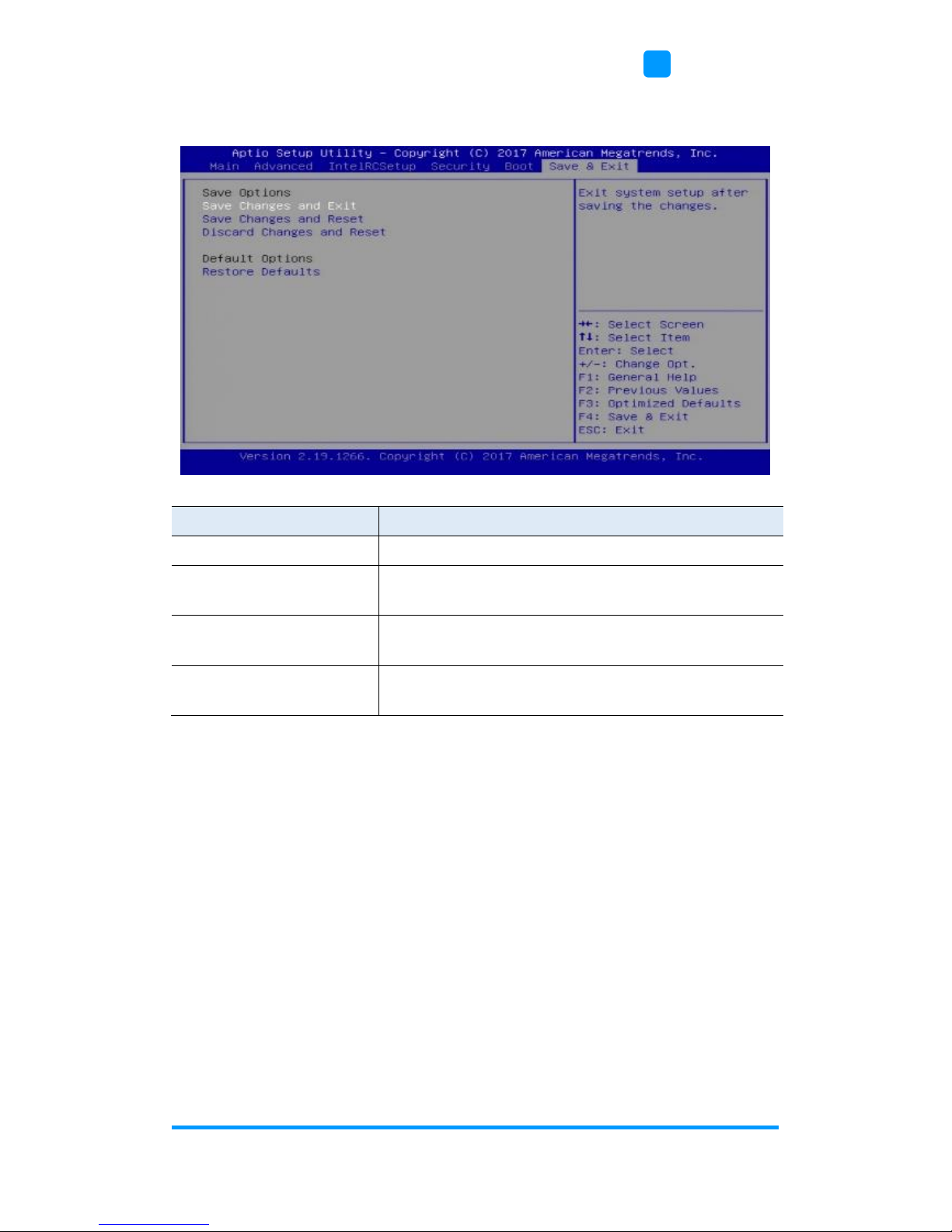
3.8 Save & Exit Settings
BIOS Setting
Description
Save Changes and Exit
Exits system setup after saving the changes.
Save Changes and
Reset
Resets the system after saving the changes.
Discard Changes and
Reset
Resets system setup without saving any changes.
Restore Defaults
Restores / Loads defaults values for all the setup
options.

52
Appendix
This section provides the mapping addresses of peripheral
devices and the sample code of watchdog timer configuration.
• I/O Port Address Map
• Interrupt Request Lines (IRQ)
• Watchdog Timer Configuration

Appendix
FWA8506 User Manual
53
A. I/O Port Address Map
Each peripheral device in the system is assigned a set of I/O port addresses
which also becomes the identity of the device. The following table lists the I/O
port addresses used.
Address
Device Description
0x00000A00-0x00000A0F
Motherboard resources
0x00000A10-0x00000A1F
Motherboard resources
0x00000A20-0x00000A2F
Motherboard resources
0x0000D000-0x0000D07F
NVIDIA GeForce GT 730
0x0000D000-0x0000D07F
Intel(R) Atom(TM) processor C3000 product
family PCIe Root Port 0 - 19A4
0x000003B0-0x000003BB
NVIDIA GeForce GT 730
0x000003B0-0x000003BB
Intel(R) Atom(TM) processor C3000 product
family PCIe Root Port 0 - 19A4
0x000003C0-0x000003DF
NVIDIA GeForce GT 730
0x000003C0-0x000003DF
Intel(R) Atom(TM) processor C3000 product
family PCIe Root Port 0 - 19A4
0x00000062-0x00000062
Microsoft ACPI-Compliant Embedded
Controller
0x00000066-0x00000066
Microsoft ACPI-Compliant Embedded
Controller
0x00000040-0x00000043
System timer
0x00000050-0x00000053
System timer
0x00007000-0x00007FFF
Intel(R) Atom(TM) processor C3000 product
family PCIe Root Port 7 - 19AB
0x0000E000-0x0000E01F
Intel(R) Atom(TM) processor C3000 product
family Legacy SMBus - 19DF
0x000003F8-0x000003FF
Communications Port (COM1)
0x000002F8-0x000002FF
Communications Port (COM2)
0x0000B000-0x0000BFFF
Intel(R) Atom(TM) processor C3000 product
family PCIe Root Port 3 - 19A7
0x00000000-0x00000CF7
PCI Express Root Complex
0x00000D00-0x0000FFFF
PCI Express Root Complex
0x00000070-0x00000077
System CMOS/real time clock
0x00000070-0x00000077
Motherboard resources

54
FWA8506 User Manual
Address
Device Description
0x00009000-0x00009FFF
Intel(R) Atom(TM) processor C3000 product
family PCIe Root Port 5 - 19A9
0x00008000-0x00008FFF
Intel(R) Atom(TM) processor C3000 product
family PCIe Root Port 6 - 19AA
0x0000002E-0x0000002F
Motherboard resources
0x0000004E-0x0000004F
Motherboard resources
0x00000061-0x00000061
Motherboard resources
0x00000063-0x00000063
Motherboard resources
0x00000065-0x00000065
Motherboard resources
0x00000067-0x00000067
Motherboard resources
0x00000080-0x00000080
Motherboard resources
0x00000092-0x00000092
Motherboard resources
0x000000B2-0x000000B3
Motherboard resources
0x00000680-0x0000069F
Motherboard resources
0x00000500-0x000005FE
Motherboard resources
0x0000C000-0x0000CFFF
Intel(R) Atom(TM) processor C3000 product
family PCIe Root Port 2 - 19A6
0x0000E050-0x0000E057
Standard SATA AHCI Controller
0x0000E040-0x0000E043
Standard SATA AHCI Controller
0x0000E020-0x0000E03F
Standard SATA AHCI Controller
0x00000020-0x00000021
Programmable interrupt controller
0x00000024-0x00000025
Programmable interrupt controller
0x00000028-0x00000029
Programmable interrupt controller
0x0000002C-0x0000002D
Programmable interrupt controller
0x00000030-0x00000031
Programmable interrupt controller
0x00000034-0x00000035
Programmable interrupt controller
0x00000038-0x00000039
Programmable interrupt controller
0x0000003C-0x0000003D
Programmable interrupt controller
0x000000A0-0x000000A1
Programmable interrupt controller
0x000000A4-0x000000A5
Programmable interrupt controller
0x000000A8-0x000000A9
Programmable interrupt controller
0x000000AC-0x000000AD
Programmable interrupt controller

Appendix
FWA8506 User Manual
55
Address
Device Description
0x000000B0-0x000000B1
Programmable interrupt controller
0x000000B4-0x000000B5
Programmable interrupt controller
0x000000B8-0x000000B9
Programmable interrupt controller
0x000000BC-0x000000BD
Programmable interrupt controller
0x000004D0-0x000004D1
Programmable interrupt controller
0x0000A000-0x0000AFFF
Intel(R) Atom(TM) processor C3000 product
family PCIe Root Port 4 - 19A8

56
FWA8506 User Manual
B. Interrupt Request Lines (IRQ)
Peripheral devices use interrupt request lines to notify CPU for the service
required. The following table shows the IRQ used by the devices on board.
Level
Function
IRQ 0
System timer
IRQ 3
Communications Port (COM2)
IRQ 4
Communications Port (COM1)
IRQ 8
System CMOS/real time clock
IRQ 11
Intel(R) Atom(TM) processor C3000 product family
Trace Hub - 19E2
IRQ 11
Intel(R) Atom(TM) processor C3000 product family
Management Engine Interface - 19D3
IRQ 11
Intel(R) Atom(TM) processor C3000 product family
Host SMBus - 19AC
IRQ 15
Intel(R) Atom(TM) processor C3000 product family
Legacy SMBus - 19DF
IRQ 16
NVIDIA GeForce GT 730
IRQ 17
High Definition Audio Controller
IRQ 23
Intel(R) Atom(TM) processor C3000 product family
RCEC - 19A2
IRQ 54 ~ IRQ 204
Microsoft ACPI-Compliant System
IRQ 256 ~ IRQ 511
Microsoft ACPI-Compliant System
IRQ 4294967096 ~
IRQ 4294967113
Intel(R) I211 Gigabit Network Connection #3
IRQ 4294967114 ~
IRQ 4294967131
Intel(R) I211 Gigabit Network Connection #5
IRQ 4294967132 ~
IRQ 4294967149
Intel(R) I211 Gigabit Network Connection #2
IRQ 4294967150 ~
IRQ 4294967167
Intel(R) I211 Gigabit Network Connection
IRQ 4294967168 ~
IRQ 4294967185
Intel(R) I211 Gigabit Network Connection #6
IRQ 4294967186 ~
IRQ 4294967203
Intel(R) I211 Gigabit Network Connection #4
IRQ 4294967204
Intel(R) USB 3.0 eXtensible Host Controller - 1.0
(Microsoft)

Appendix
FWA8506 User Manual
57
Level
Function
IRQ 4294967205 ~
IRQ 4294967222
Intel(R) Ethernet Connection X553 10 GbE SFP+ #7
IRQ 4294967223 ~
IRQ 4294967240
Intel(R) Ethernet Connection X553 10 GbE SFP+ #6
IRQ 4294967241 ~
IRQ 4294967258
Intel(R) Ethernet Connection X553 10 GbE SFP+ #8
IRQ 4294967259 ~
IRQ 4294967276
Intel(R) Ethernet Connection X553 10 GbE SFP+ #5
IRQ 4294967277 ~
IRQ 4294967284
Standard SATA AHCI Controller
IRQ 4294967285
Intel(R) Atom(TM) processor C3000 product family
PCIe Network Root Port 1 - 19D2
IRQ 4294967286
Intel(R) Atom(TM) processor C3000 product family
PCIe Network Root Port 0 - 19D1
IRQ 4294967287
Intel(R) Atom(TM) processor C3000 product family
PCIe Root Port 7 - 19AB
IRQ 4294967288
Intel(R) Atom(TM) processor C3000 product family
PCIe Root Port 6 - 19AA
IRQ 4294967289
Intel(R) Atom(TM) processor C3000 product family
PCIe Root Port 5 - 19A9
IRQ 4294967290
Intel(R) Atom(TM) processor C3000 product family
PCIe Root Port 4 - 19A8
IRQ 4294967291
Intel(R) Atom(TM) processor C3000 product family
PCIe Root Port 3 - 19A7
IRQ 4294967292
Intel(R) Atom(TM) processor C3000 product family
PCIe Root Port 2 - 19A6
IRQ 4294967293
Intel(R) Atom(TM) processor C3000 product family
PCIe Root Port 0 - 19A4
IRQ 4294967294
PCI Express Root Port

58
FWA8506 User Manual
C. Watchdog Timer Configuration
The Watchdog Timer (WDT) is used to generate a variety of output signals
after a user programmable count. The WDT is suitable for the use in the
prevention of system lock-up, such as when software becomes trapped in a
deadlock. Under these sorts of circumstances, the timer will count to zero and
the selected outputs will be driven.
Under normal circumstance, you will need to restart the WDT at regular
intervals before the timer counts to zero.
1. WDT Sample Code: The file NCT5523D.H
//--------------------------------------------------------------------------//
// THIS CODE AND INFORMATION IS PROVIDED "AS IS" WITHOUT WARRANTY OF ANY
// KIND, EITHER EXPRESSED OR IMPLIED, INCLUDING BUT NOT LIMITED TO THE
// IMPLIED WARRANTIES OF MERCHANTABILITY AND/OR FITNESS FOR A
PARTICULAR
// PURPOSE.
//
//--------------------------------------------------------------------------#ifndef __NCT5523D_H
#define __NCT5523D_H 1
//--------------------------------------------------------------------------#define NCT5523D_INDEX_PORT (NCT5523D_BASE)
#define NCT5523D_DATA_PORT (NCT5523D_BASE+1)
//--------------------------------------------------------------------------#define NCT5523D_REG_LD 0x07
//--------------------------------------------------------------------------#define NCT5523D_UNLOCK 0x87
#define NCT5523D_LOCK 0xAA
//--------------------------------------------------------------------------unsigned int Init_NCT5523D(void);
void Set_NCT5523D_LD( unsigned char);
void Set_NCT5523D_Reg( unsigned char, unsigned char);
unsigned char Get_NCT5523D_Reg( unsigned char);
//--------------------------------------------------------------------------#endif //__NCT5523D_H

Appendix
FWA8506 User Manual
59
2. WDT Sample Code: The file MAIN.CPP
//--------------------------------------------------------------------------//
// THIS CODE AND INFORMATION IS PROVIDED "AS IS" WITHOUT WARRANTY OF ANY
// KIND, EITHER EXPRESSED OR IMPLIED, INCLUDING BUT NOT LIMITED TO THE
// IMPLIED WARRANTIES OF MERCHANTABILITY AND/OR FITNESS FOR A
PARTICULAR
// PURPOSE.
//
//--------------------------------------------------------------------------#include <dos.h>
#include <conio.h>
#include <stdio.h>
#include <stdlib.h>
#include "NCT5523D.H"
//--------------------------------------------------------------------------int main (void);
void WDTInitial(void);
void WDTEnable(unsigned char);
void WDTDisable(void);
//--------------------------------------------------------------------------int main (void)
{
char SIO;
SIO = Init_NCT5523D();
if (SIO == 0)
{
printf("Can not detect Nuvoton NCT5523D, program abort.\n");
return(1);
}
WDTInitial();
WDTEnable(10);
WDTDisable();
return 0;
}
//--------------------------------------------------------------------------void WDTInitial(void)
{
unsigned char bBuf;
Set_NCT5523D_LD(0x08); //switch to logic device 8
bBuf = Get_NCT5523D_Reg(0x30);
bBuf &= (~0x01);
Set_NCT5523D_Reg(0x30, bBuf); //Enable WDTO
}
//---------------------------------------------------------------------------

60
FWA8506 User Manual
void WDTEnable(unsigned char NewInterval)
{
unsigned char bBuf;
Set_NCT5523D_LD(0x08); //switch to logic device 8
Set_NCT5523D_Reg(0x30, 0x01); //enable timer
bBuf = Get_NCT5523D_Reg(0xF0);
bBuf &= (~0x08);
Set_NCT5523D_Reg(0xF0, bBuf); //count mode is second
Set_NCT5523D_Reg(0xF1, NewInterval); //set timer
}
//--------------------------------------------------------------------------void WDTDisable(void)
{
Set_NCT5523D_LD(0x08); //switch to logic device 8
Set_NCT5523D_Reg(0xF1, 0x00); //clear watchdog timer
Set_NCT5523D_Reg(0x30, 0x00); //watchdog disabled
}
//---------------------------------------------------------------------------

Appendix
FWA8506 User Manual
61
3. WDT Sample Code: The file NCT5523D.CPP
//--------------------------------------------------------------------------//
// THIS CODE AND INFORMATION IS PROVIDED "AS IS" WITHOUT WARRANTY OF ANY
// KIND, EITHER EXPRESSED OR IMPLIED, INCLUDING BUT NOT LIMITED TO THE
// IMPLIED WARRANTIES OF MERCHANTABILITY AND/OR FITNESS FOR A
PARTICULAR
// PURPOSE.
//
//--------------------------------------------------------------------------#include "NCT5523D.H"
#include <dos.h>
//--------------------------------------------------------------------------unsigned int NCT5523D_BASE;
void Unlock_NCT5523D (void);
void Lock_NCT5523D (void);
//--------------------------------------------------------------------------unsigned int Init_NCT5523D(void)
{
unsigned int result;
unsigned char ucDid;
NCT5523D_BASE = 0x4E;
result = NCT5523D_BASE;
ucDid = Get_NCT5523D_Reg(0x20);
if (ucDid == 0xC4) //NCT5523D??
{ goto Init_Finish; }
NCT5523D_BASE = 0x2E;
result = NCT5523D_BASE;
ucDid = Get_NCT5523D_Reg(0x20);
if (ucDid == 0xC4) //NCT5523D??
{ goto Init_Finish; }
NCT5523D_BASE = 0x00;
result = NCT5523D_BASE;
Init_Finish:
return (result);
}
//--------------------------------------------------------------------------void Unlock_NCT5523D (void)
{
outportb(NCT5523D_INDEX_PORT, NCT5523D_UNLOCK);
outportb(NCT5523D_INDEX_PORT, NCT5523D_UNLOCK);
}
//---------------------------------------------------------------------------

62
FWA8506 User Manual
void Lock_NCT5523D (void)
{
outportb(NCT5523D_INDEX_PORT, NCT5523D_LOCK);
}
//--------------------------------------------------------------------------void Set_NCT5523D_LD( unsigned char LD)
{
Unlock_NCT5523D();
outportb(NCT5523D_INDEX_PORT, NCT5523D_REG_LD);
outportb(NCT5523D_DATA_PORT, LD);
Lock_NCT5523D();
}
//--------------------------------------------------------------------------void Set_NCT5523D_Reg( unsigned char REG, unsigned char DATA)
{
Unlock_NCT5523D();
outportb(NCT5523D_INDEX_PORT, REG);
outportb(NCT5523D_DATA_PORT, DATA);
Lock_NCT5523D();
}
//--------------------------------------------------------------------------unsigned char Get_NCT5523D_Reg(unsigned char REG)
{
unsigned char Result;
Unlock_NCT5523D();
outportb(NCT5523D_INDEX_PORT, REG);
Result = inportb(NCT5523D_DATA_PORT);
Lock_NCT5523D();
return Result;
}
//-----------------------------------------------------------------------
 Loading...