


FWA8408
FWA8406
1U Rackmount
Network Appliance
User’s Manual
Version 1.0
(Aug. 2017)

ii
FWA8408 & FWA8406 User Manual
Copyright
© 2017 IBASE Technology, Inc. All rights reserved.
No part of this publication may be reproduced, copied, stored in a retrieval system, translated
into any language or transmitted in any form or by any means, electronic, mechanical,
photocopying, or otherwise, without the prior written consent of IBASE Technology, Inc.
(hereinafter referred to as “IBASE”).
Disclaimer
IBASE reserves the right to make changes and improvements to the products described in
this document without prior notice. Every effort has been made to ensure the information in
the document is correct; however, IBASE does not guarantee this document is error-free.
IBASE assumes no liability for incidental or consequential damages arising from
misapplication or inability to use the product or the information contained herein, nor for any
infringements of rights of third parties, which may result from its use.
Trademarks
All the trademarks, registrations and brands mentioned herein are used for identification
purposes only and may be trademarks and/or registered trademarks of their respective
owners.

FWA8408 & FWA8406 User Manual
iii
Compliance
This product has passed CE tests for environmental specifications and limits. This
product is in accordance with the directives of the Union European (EU). If users
modify and/or install other devices in this equipment, the CE conformity declaration
may no longer apply.
This product has been tested and found to comply with the limits for a Class A
device, pursuant to Part 15 of the FCC Rules. These limits are designed to provide
reasonable protection against harmful interference in a residential installation. This
equipment generates, uses and can radiate radio frequency energy and, if not
installed and used in accordance with manufacturer’s instructions, may cause
harmful interference to radio communications.
WEEE
This product must not be disposed of as normal household waste, in
accordance with the EU directive of for waste electrical and electronic
equipment (WEEE - 2012/19/EU). Instead, it should be disposed of by
returning it to a municipal recycling collection point. Check local
regulations for disposal of electronic products.
Green IBASE
This product is compliant with the current RoHS restrictions and
prohibits use of the following substances in concentrations exceeding
0.1% by weight (1000 ppm) except for cadmium, limited to 0.01% by
weight (100 ppm).
• Lead (Pb)
• Mercury (Hg)
• Cadmium (Cd)
• Hexavalent chromium (Cr6+)
• Polybrominated biphenyls (PBB)
• Polybrominated diphenyl ether (PBDE)

iv
FWA8408 & FWA8406 User Manual
Important Safety Information
Carefully read the precautions before using the device.
Environmental conditions:
• Lay the device horizontally on a stable and solid surface in case the device may
fall, causing serious damage.
• Slots and openings on the chassis are for ventilation. Do not block or cover these
openings. Make sure you leave plenty of space around the device for ventilation.
NEVER INSERT OBJECTS OF ANY KIND INTO THE VENTILATION
OPENINGS.
• Use this product in environments at ambient temperatures 0˚C ~ 40˚.
• DO NOT LEAVE THIS DEVICE IN AN ENVIRONMENT WHERE THE
STORAGE TEMPERATURE MAY GO BELOW -20˚C OR ABOVE 70˚C. This
could damage the device. The device must be used in a controlled environment.
Care for your IBASE products:
• Before cleaning the device, turn it off and unplug all cables such as power in case
a small amount of electrical current may still flow.
• Use neutral cleaning agents or diluted alcohol to clean the device chassis with a
cloth. Then wipe the chassis with a dry cloth.
• Vacuum the dust with a computer vacuum cleaner to prevent the air vent or slots
from being clogged.
WARNING
Attention during use:
• Do not use this product near water.
• Do not spill water or any other liquids on your device.
• Do not place heavy objects on the top of the device.
• Operate this device from the type of power indicated on the marking label. If you
are not sure of the type of power available, consult your distributor or local
power company.
• Do not walk on the power cord or allow anything to rest on it.
• If you use an extension cord, make sure that the total ampere rating of the
product plugged into the extension cord does not exceed its limits.
• When handling processor chips or memory modules, avoid touching their pins or
gold fingers. Put modules or peripherals back into antistatic bags when they are
not in use or not installed in the chassis.
Avoid Disassembly
You are not suggested to disassemble, repair or make any modification to the device.
Disassembly, modification, or any attempt at repair could generate hazards and
cause damage to the device, even bodily injury or property damage, and will void any
warranty.

FWA8408 & FWA8406 User Manual
v
CAUTION
Danger of explosion if internal lithium-ion battery is replaced by an incorrect type.
Replace only with the same or equivalent type recommended by the manufacturer.
Dispose of used batteries according to the manufacturer’s instructions. Under no
circumstances should the Lithium battery cell be shorted; otherwise the battery cell
may heat up or cause potential burn hazards.
Warranty Policy
• IBASE standard products:
24-month (2-year) warranty from the date of shipment. If the date of shipment
cannot be ascertained, the product serial numbers can be used to determine
the approximate shipping date.
• 3rd-party parts:
12-month (1-year) warranty from delivery for the 3rd-party parts that are not
manufactured by IBASE, such as CPU, memory, HDD, power adapter, panel
and touchscreen.
* PRODUCTS, HOWEVER, THAT FAILS DUE TO MISUSE, ACCIDENT,
IMPROPER INSTALLATION OR UNAUTHORIZED REPAIR SHALL BE
TREATED AS OUT OF WARRANTY AND CUSTOMERS SHALL BE BILLED
FOR REPAIR AND SHIPPING CHARGES.
Technical Support & Services
1. Visit the IBASE website at www.ibase.com.tw to find the latest information about
the product.
2. If you need any further assistance from your distributor or sales representative,
prepare the following information of your product and elaborate upon the
problem.
• Product model name
• Product serial number
• Detailed description of the problem
• The error messages in text or in screenshots if there is any
• The arrangement of the peripherals
• Software in use (such as OS and application software, including the version
numbers)
3. If repair service is required, you can download the RMA form at
http://www.ibase.com.tw/english/Supports/RMAService/. Fill out the form and
contact your distributor or sales representative.

vi
FWA8408 & FWA8406 User Manual
Table of Contents
Compliance.................................................................................................... iii
Important Safety Information ....................................................................... iv
WARNING ...................................................................................................... iv
CAUTION ........................................................................................................ v
Warranty Policy .............................................................................................. v
Technical Support & Services ...................................................................... v
Chapter 1 General Information ................................................................ 1
1.1 Introduction ............................................................................................. 2
1.2 Features .................................................................................................. 3
1.3 Packing List ............................................................................................ 3
1.4 Optional Accessories .............................................................................. 3
1.5 Specifications .......................................................................................... 4
1.6 Overview ................................................................................................. 6
1.7 Dimensions ............................................................................................. 8
Chapter 2 Hardware Configuration ....................................................... 12
2.1 Essential Installations Before You Begin ............................................... 13
2.1.1 CPU Installation / Replacement .............................................. 14
2.1.2 Memory Installation / Replacement ......................................... 15
2.1.3 HDD Installation / Replacement .............................................. 16
2.1.4 CF Card & IPMI Module Installation / Replacement ................ 18
2.1.5 Fan Module Installation / Replacement ................................... 19
2.1.6 Redundant Power Supply Unit Installation / Replacement ...... 19
2.1.7 IBN Module Installation / Replacement ................................... 20
2.2 Setting the Jumpers .............................................................................. 21
2.2.1 How to Set Jumpers ............................................................... 21
2.3 Jumper & Connector Locations on Motherboard ................................... 22
2.4 Jumpers Quick Reference ..................................................................... 24
2.4.1 ME Register Clearance (JBAT3) .......................................... 24
2.4.2 CMOS Data Clearance (JBAT4) ........................................... 25
2.5 Connectors Quick Reference ................................................................ 26
2.5.1 System Function Connector (JP3) ........................................ 27
2.5.2 Digital I/O Port (JP4) ................................ ............................ 29

FWA8408 & FWA8406 User Manual
vii
Chapter 3 BIOS Setup ............................................................................ 30
3.1 Introduction ........................................................................................... 31
3.2 BIOS Setup ........................................................................................... 31
3.3 Main Settings ........................................................................................ 32
3.4 Advanced Settings ................................................................................ 33
3.4.1 CPU Configuration .................................................................. 33
3.4.2 Trusted Computing ................................................................. 34
3.4.3 SATA Configuration ................................................................ 35
3.4.4 SMART Setting ................................................................ ....... 35
3.4.5 NCT5523D Super IO Configuration ........................................ 36
3.4.6 Hardware Monitor ................................................................... 39
3.4.7 LAN Bypass Configuration ...................................................... 40
3.4.8 Console Port Configuration ..................................................... 40
3.4.9 USB Configuration .................................................................. 42
3.5 Security Settings ................................................................................... 43
3.6 Boot Settings......................................................................................... 44
3.7 Save & Exit Settings.............................................................................. 45
3.8 Server Management.............................................................................. 46
3.8.1 BMC SOL Function ................................................................. 47
3.8.2 BMC Network Configuration ................................................... 48
Appendix ...................................................................................................... 49
A. I/O Port Address Map ............................................................................ 50
B. Interrupt Request Lines (IRQ) ............................................................... 55
C. Digital I/O Sample Code ........................................................................ 59
D. Watchdog Timer Configuration .............................................................. 64

1
Chapter 1
General Information
The information provided in this chapter includes:
• Features
• Packing List
• Optional Accessories
• Specifications
• Overview
• Dimensions

2
FWA8408 & FWA8406 User Manual
1.1 Introduction
FWA8408 & FWA8406 series are specifically designed for the network
security and management market. There are plenty of applications adopting
network security or network management as listed below.
FWA8408 & FWA8406 include the following models:
• FWA8408 (with a single PSU)
• FWA8408-RPSU (with 1+1 redundant PSU)
• FWA8406 (with a single PSU)
• FWA8406-RPSU (with 1+1 redundant PSU)
Photo of FWA8408
Photo of FWA8406
Network Security Applications:
• Firewall
• Unified Threat Management (UTM)
• Virtual Private Network (VPN)
• Proxy Server
• Caching Server
Network Management Applications:
• Load balancing
• Quality of Service
• Remote Access Service
The FWA networking appliance product line covers the spectrum from offering
platforms designed for:
• SOHO
• SMB
• Enterprise
Each product is designed to address the distinctive requirements of its
respective market segment from cost effective entry-level solutions to high
throughput and performance-bound systems for the enterprise level.

General Information
FWA8408 & FWA8406 User Manual
3
1
1.2 Features
• 1U rackmount platform designed with Intel
®
Xeon® 6th Gen. Core™
i7/i5/i3 processor
• DDR4 DIMM 2133 MHz (ECC supported per CPU SKUs)
• GbE LAN ports with 2 advanced LAN Bypass pairs
• Optional IPMI 2.0 module to output through VGA port for FWA8408
• CF slot and PCIe (x8) expansion slot(s)
• 250W single power supply or 300W 1+1 redundant power supply
1.3 Packing List
Your product package should include the items listed below. If any of the
items below is missing, contact the distributor or the dealer from whom you
purchased the product.
Models with a single PSU:
• FWA8408 / FWA8406 x 1
• Power Cord x 1
• CPU Heatsink x 1
• Rack Mount Bracket x 2
Models with 1+1 redundant PSU:
• FWA8408-RPSU / FWA8406-RPSU x 1
• Power Cord x 2
• CPU Heatsink x 1
• Rack Mount Bracket x 2
1.4 Optional Accessories
IBASE provide optional accessories as follows. Please contact us or your
dealer if you need any.
• Console Cable (160 cm, PK1-51)
• VGA Cable (40 cm, VGA21A)

4
FWA8408 & FWA8406 User Manual
1.5 Specifications
Product Name
FWA8408
FWA8406
System
Motherboard
MBN800-8L
MBN800-6L
Operating
System
• Windows 10 (64-bit)
• Linux Ubuntu 16.04.3
CPU
Intel® Xeon® / 6th Gen. Core™
i7/i5/i3 processor LGA1151
Intel® 6th Gen. Core™ i7/i5/i3
processor LGA1151
Chipset
Intel® C236 PCH
Intel® H110 PCH
Memory
4 x DDR4 DIMM 2133 MHz,
expandable to 64 GB
* ECC supported per CPU
SKUs
2 x DDR4 DIMM 2133 MHz,
expandable to 32 GB
(non-ECC)
Storage
• 2 x 2.5” / 3.5” HDD or SSD drive bay
• On-board CF slot
Network
8 x Intel® I210AT GbE
6 x Intel® I211AT GbE
Bypass
2 x segments (LAN1 / LAN2 & LAN3 / LAN4)
NIC Slot
1 x IBN card series
N/A
Super I/O
Nuvoton NCT5523D
IPMI
IPMI module compliant with
IPMI 2.0 (Optional)
N/A
Power Supply
• Full range 250W ATX power supply
• For RPSU type: Full range 300W 1+1 redundant power
supply
Power
Requirement
100 ~ 240V AC
BIOS
AMI BIOS
TPM
1.2
Watchdog
Watchdog Timer 256 segments, 0, 1, 2…255 sec/min
Chassis
Steel with textured black color paint
Dimensions
(W x H x D)
438 x 44 x 422 mm (17.24” x 1.73” x 16.61”)
Weight
9 kg (19.84 lb)
Certificate
CE / FCC Class A / LVD

General Information
FWA8408 & FWA8406 User Manual
5
1
Product Name
FWA8408
FWA8406
Front I/O Ports
Console
1 x Console port
Traffic LAN
Port
8 x RJ45 GbE LAN ports
6 x RJ45 GbE LAN ports
USB
2 x USB 3.0
Rear I/O Ports
AC Power
Inlet
• 1 x AC inlet 100 ~ 240V, full range 250W, single power
supply (for FWA8408 & FWA8406)
• 2 x AC inlet 100 ~ 240V, full range 300W, 1+1 redundant
power supply (for FWA8408-RPSU & FWA8406-RPSU)
CF
1 x CF slot
Display
1 x VGA port (Reserved and optional)
Fan
3 x system fan module
Expansion
• 1 or 2 x PCIe (x8) slot
• 1 x mini-PCIe slot with
PCIe, USB & SATA
• 1 x M.2 M2280
1 x PCIe (x8) slot
Environment
Temperature
• Operating: 0 ~ 40 °C (32 ~ 104 °F)
• Storage: -20~ 70 °C (-4 ~ 158 °F)
Relative
Humidity
5 ~ 90%
Vibration
Protection
• Operating: 0.25 Grms / 3 ~ 500 Hz (Z-axis)
• Non-operating: 1.0 Grms / 3 ~ 500Hz (Z-axis)
Shock
Protection
Sawtooth wave 40G
All specifications are subject to change without prior notice.

6
FWA8408 & FWA8406 User Manual
1.6 Overview
Front View
No.
Name
No.
Name
1
LCM Display with 4 buttons
5
Reserved Area
(FWA8408: for IBN module or
HDD
FWA8406: for HDD)
2
LED Indicators
(from top to bottom: Status,
HDD, Power)
6
USB 3.0 Ports
3
Console Port
7
Factory Default Button
(GPIO Signal)
4
GbE LAN Ports
Oblique View
• FWA8408 / FWA8408-RPSU
• FWA8406 / FWA8406-RPSU
General Information
FWA8408 & FWA8406 User Manual
7
1
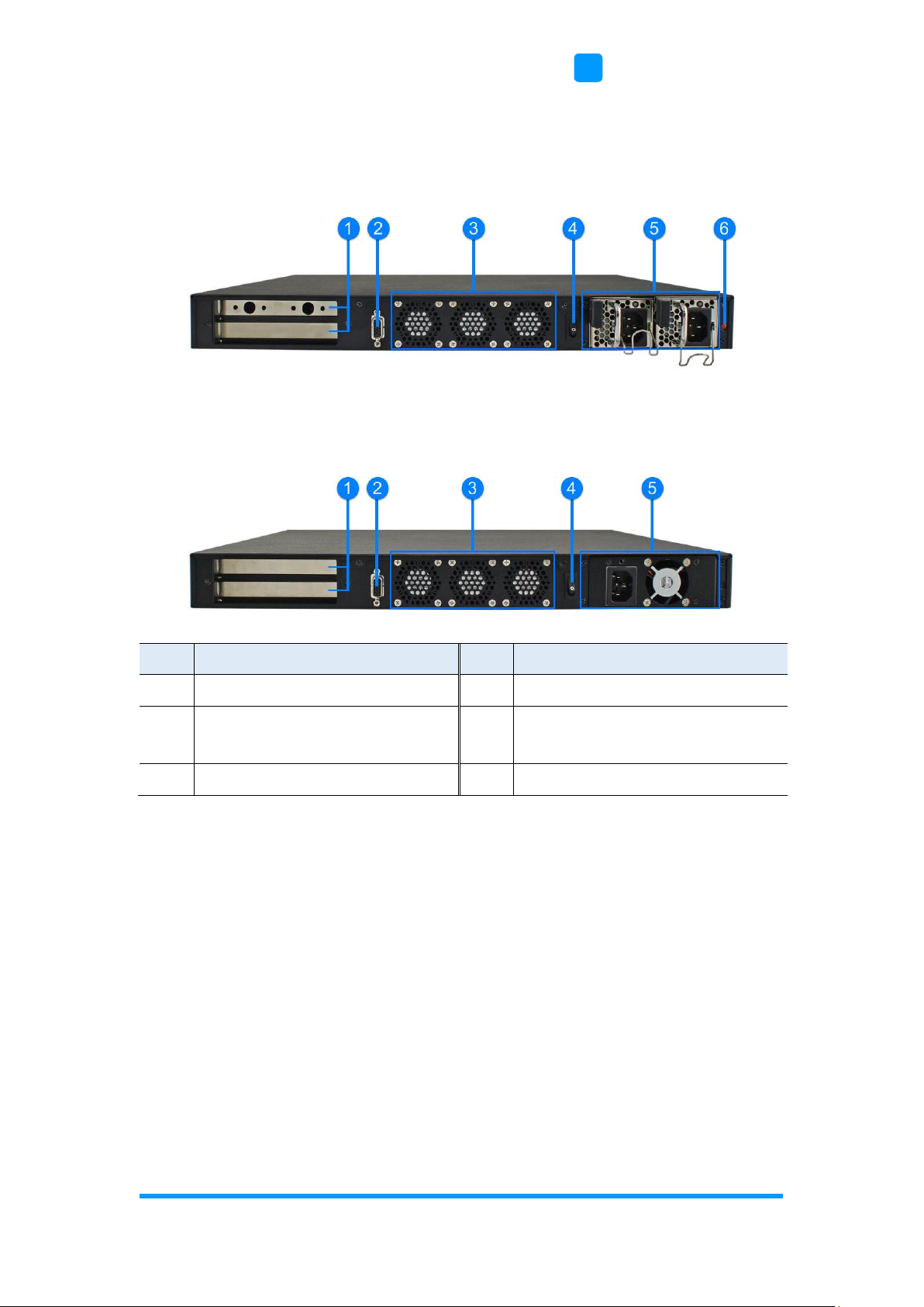
Rear View
• Models with redundant PSUs (FWA8408-RPSU / FWA8406-RPSU)
• Models with a single PSU (FWA8408 / FWA8406)
No.
Name
No.
Name
1
Expansion Slots
4
Power Switch
2
VGA Port
(Reserved & optional)
5
Single PSU / Reduntant PSU
3
System Fans
6
Alarm Beep Switch*
* The alarm beep switch allows you to turn on or off the alarm beep sound that
goes off as one of the redundant power supplies is out of work.

8
FWA8408 & FWA8406 User Manual
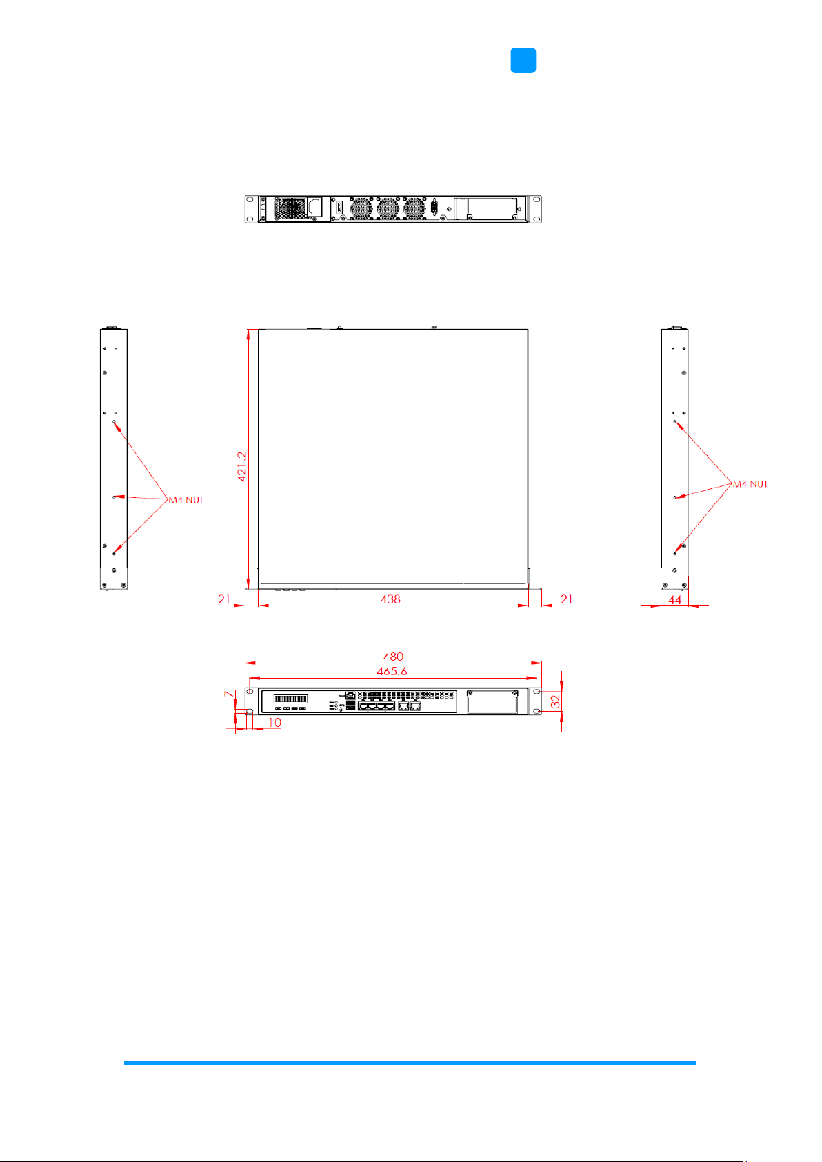
1.7 Dimensions
Unit: mm
• FWA8408-RPSU

General Information
FWA8408 & FWA8406 User Manual
9
1
Unit: mm
• FWA8408

10
FWA8408 & FWA8406 User Manual
Unit: mm
• FWA8406-RPSU
General Information
FWA8408 & FWA8406 User Manual
11
1
Unit: mm
• FWA8406

12
Chapter 2
Hardware Configuration
The information provided in this chapter includes:
• Essential installations before you begin
• Information and locations of connectors
Hardware Configuration
FWA8408 & FWA8406 User Manual
13
2
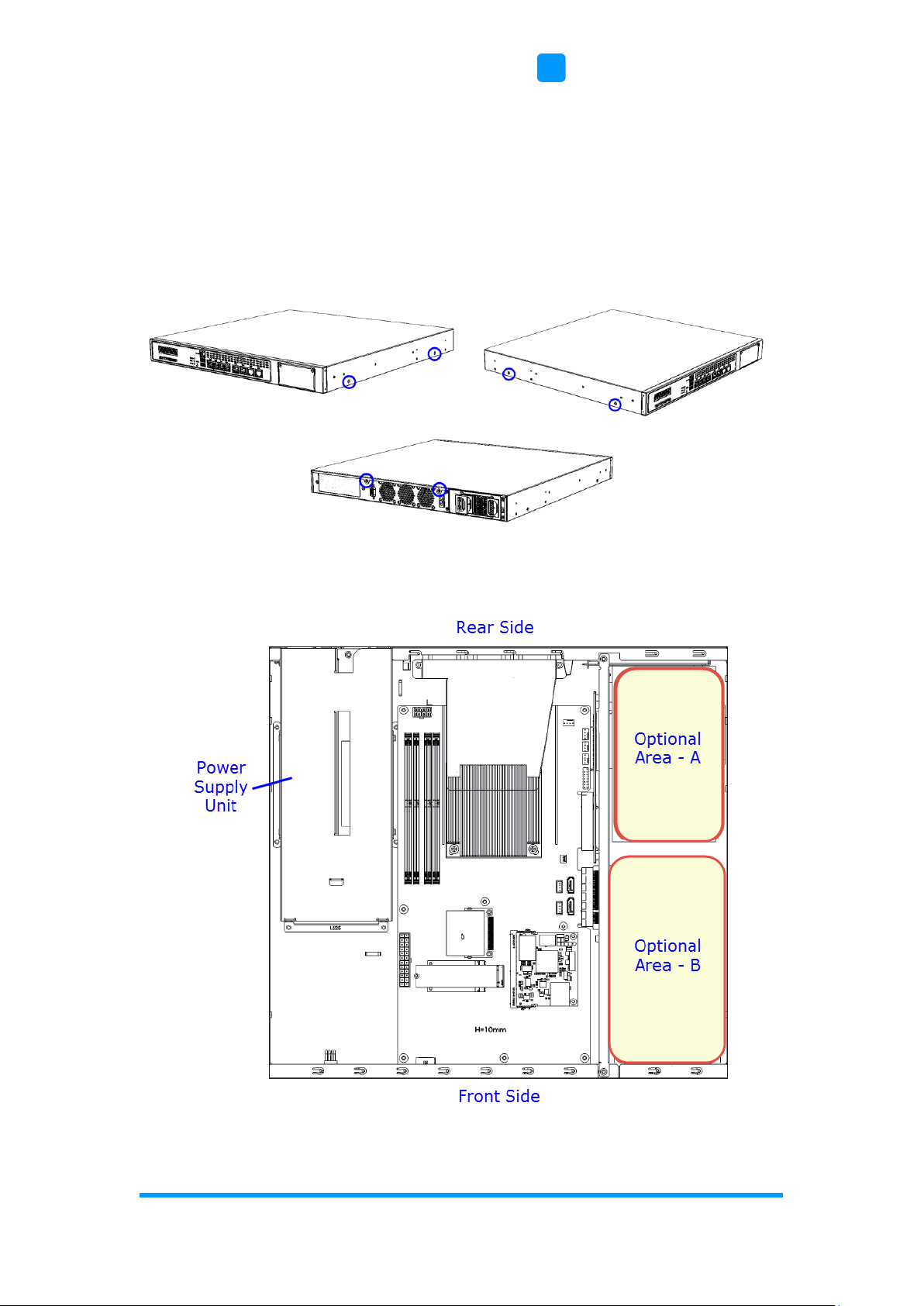
2.1 Essential Installations Before You Begin
For installation or replacement of CPU, memory modules, HDD/SSD, CF card,
IPMI card & mini-PCIe card (IPMI & mini-PCIe slots are both available for
FWA8408 only), fans, you need to disassemble the device cover first by
loosening 6 screws. This is illustrated by the example of FWA8408 as below.
Configuration inside FWA8408 & FWA8406:
Areas A and B allow for optional HDD/SSD and expansion cards installation.

14
FWA8408 & FWA8406 User Manual
2.1.1 CPU Installation / Replacement
Follow the instructions below to install or replace the CPU if necessary.
1. Take away the wind scooper as marked below. Then remove the CPU
heatsink.
2. Unlock the CPU socket by pressing the lever sideways, then lift up the
lever and the metal lid.
3. Position the CPU above the socket such that the CPU corner aligns with
the gold triangle matching the socket corner with a small triangle.
4. Carefully insert the CPU into the socket and push down the lever to
secure the CPU.
Then you can install the CPU cooler and fan back.
Note: Ensure that the CPU cooler and the CPU top surface are in total contact
to avoid CPU overheating problem that would cause your system to hang
or be unstable.

Hardware Configuration
FWA8408 & FWA8406 User Manual
15
2
2.1.2 Memory Installation / Replacement
If you need to install or replace a memory module, follow the instructions
below for installation after you disassemble the device cover.
1. Locate the memory slots in the device.
2. Press the ejector tab of the memory slot down and outwards with your
fingertips.
3. Hold the memory module and align the key of the module with that on the
memory slot.
4. Gently push the module in an upright position until the ejector tabs of the
memory slot close to hold the module in place when the module touches
the bottom of the slot.
To remove the module, press the ejector tabs outwards with your fingertips to
eject the module.

16
FWA8408 & FWA8406 User Manual
2.1.3 HDD Installation / Replacement
After you disassemble the device cover, you can see the optional areas A and
B as shown below allow for optional HDD/SSD and expansion cards
installation. If you need to install or replace an HDD/SDD, follow the
instructions below for installation.
1. Remove 4 screws for each HDD/SSD (8 screws for two HDD/SSD) and
take out from the tray.
2. Install a new HDD/SDD onto the tray and fasten 4 screws for each
HDD/SDD.

Hardware Configuration
FWA8408 & FWA8406 User Manual
17
2
3. Secure the tray with HDD from the bottom of the device. Note the screw
holes for different sizes of HDD/SSD as ilustrated below.

18
FWA8408 & FWA8406 User Manual
2.1.4 CF Card & IPMI Module Installation / Replacement
If you need to install a CF card or an IPMI module, remove the device cover
firstly and then follow the instructions below.
Note: IPMI module is optional for purchase.
IPMI module:
1. Locate the IPMI slot and align the key of the module with that on the slot.
2. Insert the module slantwise and gently push the module straight down
until the clips of the slot close to hold the module in place when the
module touches the bottom of the slot.
.
To remove the module, press the clips outwards with your thumb and index
finger of both hands.
CF card:
Locate the CF slot and Insert the CF card to the slot.
To remove the CF card or IPMI module, pull it out with your thumb and index
finger directly.

Hardware Configuration
FWA8408 & FWA8406 User Manual
19
2
2.1.5 Fan Module Installation / Replacement
If you need to install or replace a fan module, after disassembling the device
cover, release 4 screws of the fan module on the rear side of the device, take
out the fan, replace with a new one, and tighten these screws.
2.1.6 Redundant Power Supply Unit Installation / Replacement
If you need to install or replace a redundant power supply unit, push the latch
downwards, grasp the handle, pull the PSU out carefully and replace with a
new one.

20
FWA8408 & FWA8406 User Manual
2.1.7 IBN Module Installation / Replacement
IBN module is optional for FWA8408 only. To install or replace an IBN
module, follow the steps below.
1. Remove the IBN door by releasing two screws as below.
2. Install the module into the device.
3. Note the screw holes for IBN rail bracket as ilustrated below.

Hardware Configuration
FWA8408 & FWA8406 User Manual
21
2
2.2 Setting the Jumpers
Set up and configure your FWA8408 & FWA8406 by using jumpers for various
settings and features according to your needs and applications. Contact your
supplier if you have doubts about the best configuration for your use.
2.2.1 How to Set Jumpers
Jumpers are short-length conductors consisting of several metal pins with a
non-conductive base mounted on the circuit board. Jumper caps are used to
have the functions and features enabled or disabled. If a jumper has 3 pins,
you can connect either PIN1 to PIN2 or PIN2 to PIN3 by shorting.
A 3-pin jumper
A jumper cap
Refer to the illustration below to set jumpers.
Pin closed
Oblique view
Schematic illustration in the manual
Open
1-2
2-3
When two pins of a jumper are encased in a jumper cap, this jumper is
closed, i.e. turned On.
When a jumper cap is removed from two jumper pins, this jumper is open, i.e.
turned Off.
Pin# 1
2
3
1 2 3
1 2 3
1 2 3
22
FWA8408 & FWA8406 User Manual
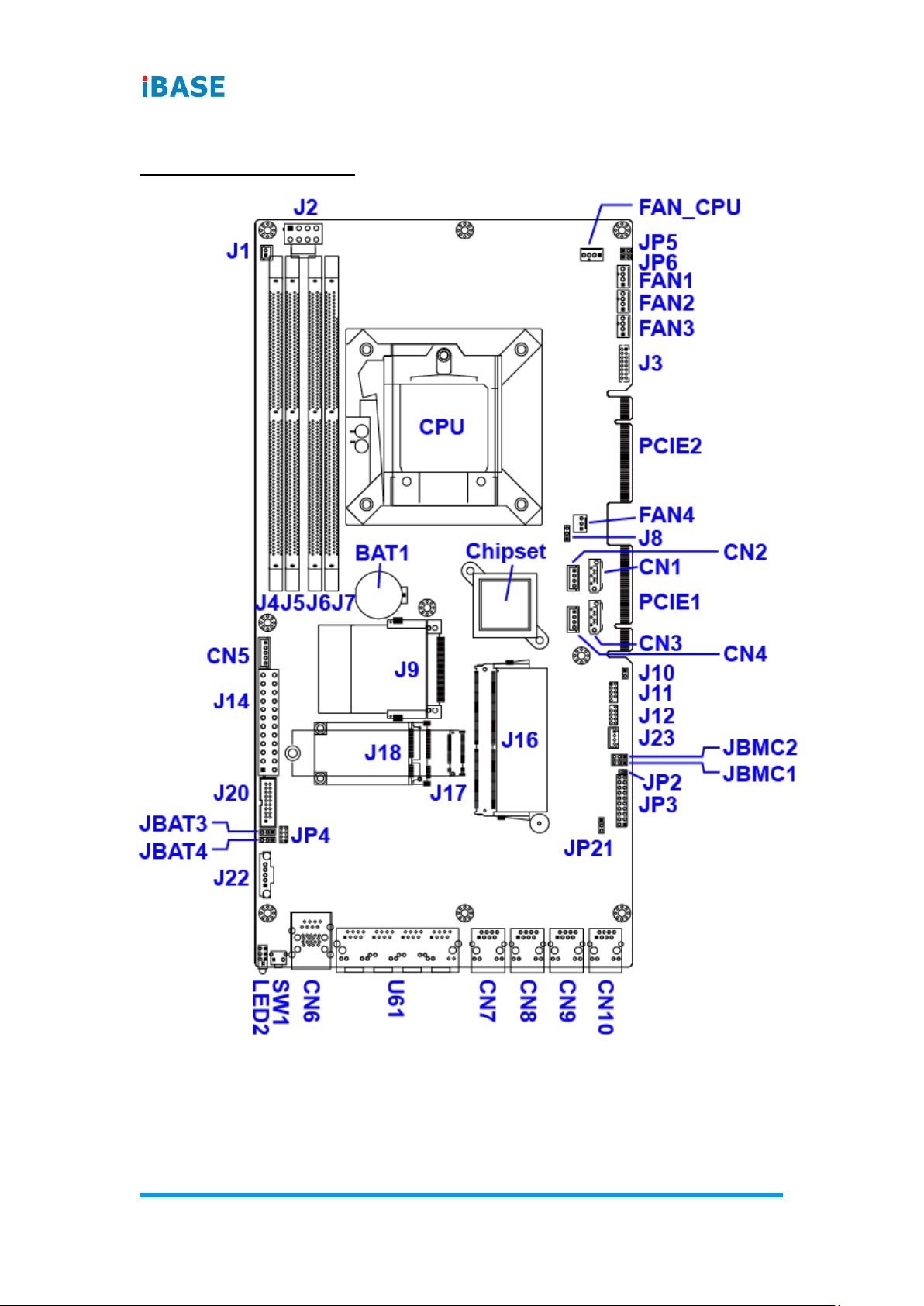
2.3 Jumper & Connector Locations on Motherboard
Motherboard: MBN800-8L

Hardware Configuration
FWA8408 & FWA8406 User Manual
23
2
Motherboard: MBN800-6L

24
FWA8408 & FWA8406 User Manual
2.4 Jumpers Quick Reference
Function
Connector Name
Page
ME Register Clearance
JBAT3
24
CMOS Data Clearance
JBAT4
25
2.4.1 ME Register Clearance (JBAT3)
Function
Pin closed
Illustration
Normal
(default)
1-2
Clear ME Register
2-3
1
1
1

Hardware Configuration
FWA8408 & FWA8406 User Manual
25
2
2.4.2 CMOS Data Clearance (JBAT4)
Function
Pin closed
Illustration
Normal
(default)
1-2
Clear CMOS
2-3
1
1
1

26
FWA8408 & FWA8406 User Manual
2.5 Connectors Quick Reference
Function
Connector Name
Page
System Function Connector
JP3
26
Digital I/O Port
JP4
29
External SATA Power
CN2, CN4
--
LCM Port
CN5
--
Fan Connector
FAN_CPU, FAN1, FAN2, FAN3,
FAN4
-System Power Switch
J1
--
ATX Power Connector
J2, J14
--
External VGA Port
J3
--
IPMI Connector*
J16
--
M.2 M2280 Slot*
J17
--
Mini-PCIe Slot*
J18
--
USB 3.0 Port
J20
--
DDR4 Slot
FWA8408: J4, J5, J6, J7
1-1
FWA8406: J5, J7
--
LAN Port
FWA8408:
U61 (quadruple),
CN7, CN8, CN9, CN10 (single)
1-2
FWA8406:
U61 (quadruple),
CN7, CN8 (single)
--
CF Card Slot
J9
--
SATA 3.0 Port
CN1, CN3
--
Console Port & USB 3.0 Ports
CN6
--
PCIe Gold Finger
FWA8408:
PCIE1 (with x8 / x4 / x4 signals)
PCIE2 (with x8 signals)
FWA8406:
PCIE2 (with x8 signals)
--
Factory Use Only
J11, J12, J23
--
* Available only for FWA8408

Hardware Configuration
FWA8408 & FWA8406 User Manual
27
2
2.5.1 System Function Connector (JP3)
Pin
Assigment
Pin
Assigment
1
VCC5
2
SPEAKER
3
NC
4
NC
5
GND
6
GND
7
NC
8
VCC5
9
5VDUAL
10
BYPASS8_LED-
11
5VDUAL
12
BYPASS9_LED-
13
GND
14
ATXPWR_BTN#
15
NC
16
NC
17
GND
18
FRST_OUT
19
VCC3_3
20
-HDD_LED
JP3 is utilized for system indicators to provide light indication of the computer
activities and switches to change the computer status. It provides interfaces
for the following functions.
2
20 19
1

28
FWA8408 & FWA8406 User Manual
• ATX Power ON Switch (Pins 13 and 14)
The 2 pins make an “ATX Power Supply On/Off Switch” for the system
that connects to the power switch on the case. When pressed, the power
switch will force the system to power on. When pressed again, it will
power off the system.
• Hard Disk Drive LED Connector (Pins 19 and 20)
This connector connects to the hard drive activity LED on control panel.
This LED will flash when the HDD is being accessed.
• Reset Switch (Pins 17 and 18)
The reset switch allows you to reset the system without turning the main
power switch off and then on again. Orientation is not required when
making a connection to this header.
• Power LED (Pins 1, 3 and 5)
This connector connects to the system power LED on control panel. This
LED will light when the system turns on.
• Bypass LED1 (Pins 9 and 10)
The two pins make an external LED connector light for LAN bypass.
• Bypass LED2 (Pins 11 and 12)
The two pins make an external LED connector light for LAN bypass.

Hardware Configuration
FWA8408 & FWA8406 User Manual
29
2
2.5.2 Digital I/O Port (JP4)
Pin
Assigment
Pin
Assigment
1
GND
2
5VDUAL
3
INT0_SIOGP22
4
INT0_SIOGP25
5
INT0_SIOGP23
6
INT0_SIOGP26
7
INT0_SIOGP24
8
INT0_SIOGP27
1
2
8
7

30
Chapter 3
BIOS Setup
This chapter describes the different settings available in the AMI
BIOS that comes with the board. The topics covered in this
chapter are as follows:
• Main Settings
• Advanced Settings
• Chipset Settings
• Security Settings
• Book Settings
• Save & Exit

BIOS Setup
FWA8408 & FWA8406 User Manual
31
4
3.1 Introduction
The BIOS (Basic Input/Output System) installed in the ROM of your computer
system supports Intel® processors. The BIOS provides critical low-level
support for standard devices such as disk drives, serial ports and parallel
ports. It also provides password protection as well as special support for
detailed fine-tuning of the chipset controlling the entire system.
3.2 BIOS Setup
The BIOS provides a Setup utility program for specifying the system
configurations and settings. The BIOS ROM of the system stores the Setup
utility. When you turn on the computer, the BIOS is immediately activated.
Press the <Del> key immediately allows you to enter the Setup utility. If you
are a little bit late pressing the <Del> key, POST (Power On Self Test) will
continue with its test routines, thus preventing you from invoking the Setup.
If you still need to enter Setup, restart the system by pressing the ”Reset”
button or simultaneously pressing the <Ctrl>, <Alt> and <Delete> keys.
You can also restart by turning the system Off and back On again.
The following message will appear on the screen:
Press <DEL> to Enter Setup
In general, press the arrow keys to highlight items, <Enter> to select, the
<PgUp> and <PgDn> keys to change entries, <F1> for help, and <Esc> to
quit.
When you enter the BIOS Setup utility, the Main Menu screen will appear on
the screen. The Main Menu allows you to select from various setup functions
and exit choices.
Warning: It is strongly recommended that you avoid making any changes to
the chipset defaults.
These defaults have been carefully chosen by both AMI and your
system manufacturer to provide the absolute maximum
performance and reliability. Changing the defaults could make the
system unstable and crash in some cases.

32
FWA8408 & FWA8406 User Manual
3.3 Main Settings
BIOS Setting
Description
System Date
Sets the date.
Use the <Tab> key to switch between the data
elements.
System Time
Set the time.
Use the <Tab> key to switch between the data
elements.

BIOS Setup
FWA8408 & FWA8406 User Manual
33
4
3.4 Advanced Settings
This section allows you to configure, improve your system and allows you to
set up some system features according to your preference.
3.4.1 CPU Configuration
BIOS Setting
Description
Intel(R) SpeedStep (tm)
Enables / Disables the function to allow more
than two frequency ranges to be supported.
Turbo Mode
Enables / Disables Turbo Mode.
34
FWA8408 & FWA8406 User Manual
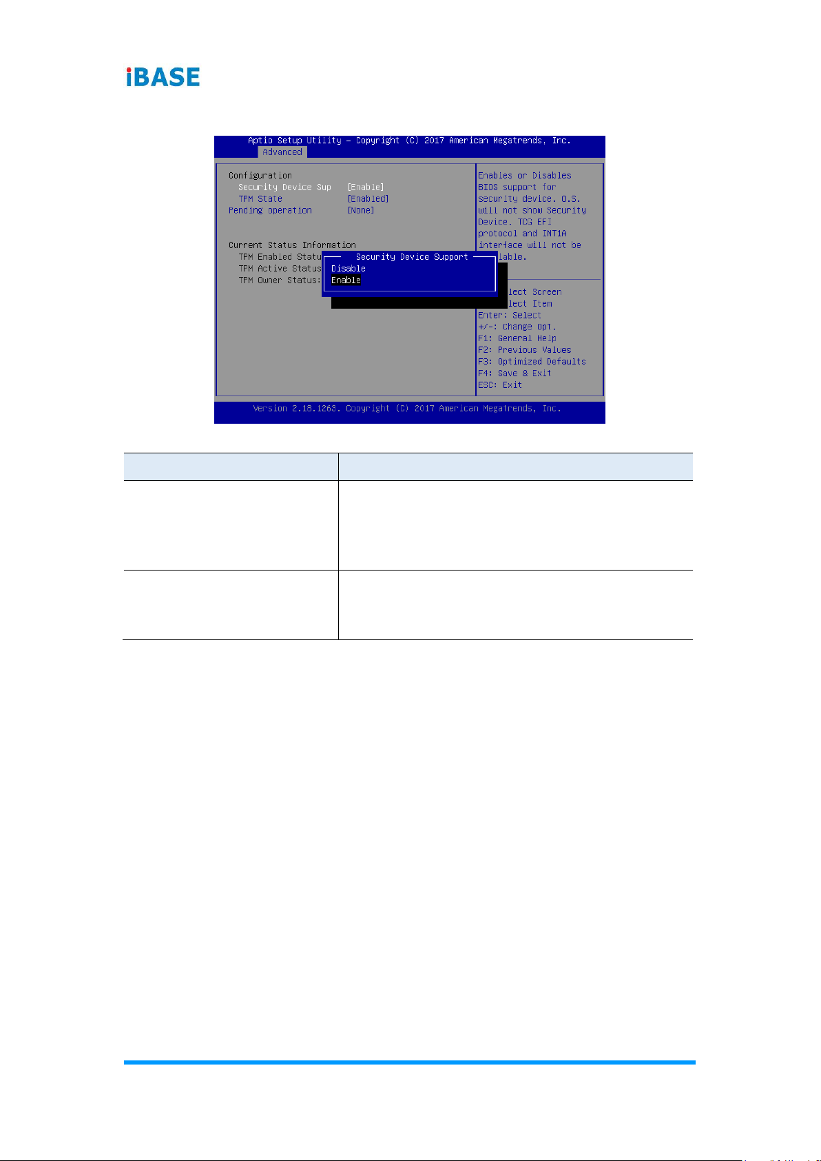
3.4.2 Trusted Computing
BIOS Setting
Description
Security Device Support
Enables / Disables TPM support. O.S. will not
show TPM. Reset of platform is required.
Note: This feature is not supported on
IB990AF-C236.
Pending operation
Schedule an operation for the security device.
Note: Your computer will reboot during restart
in order to change the state of security device.
BIOS Setup
FWA8408 & FWA8406 User Manual
35
4
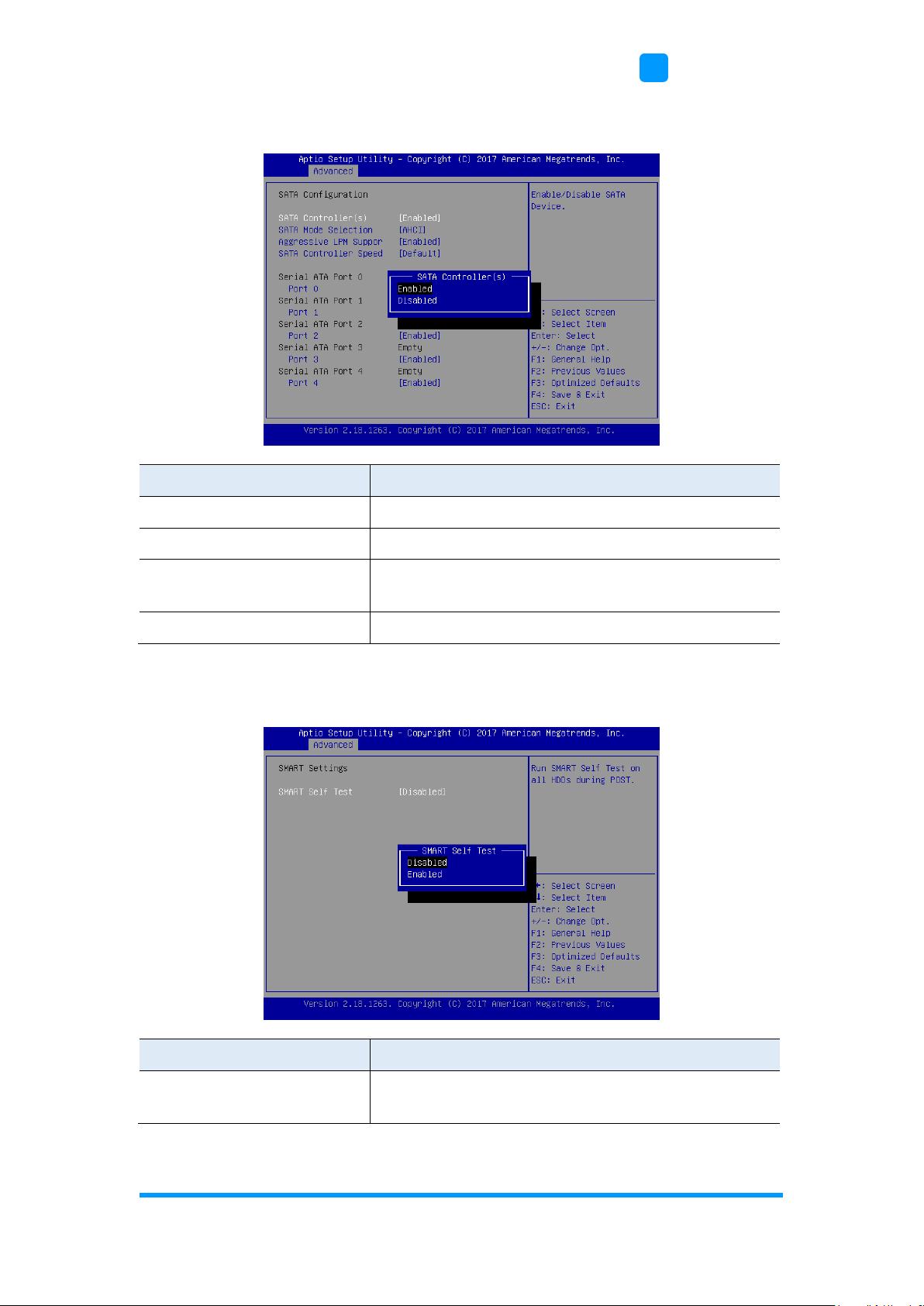
3.4.3 SATA Configuration
BIOS Setting
Description
SATA Controller(s)
Enables / Disables SATA device.
SATA Mode Selection
Selects IDE / AHCI Mode.
SATA Controller Speed
Selects the SATA controller speed as Default /
Gen1 / Gen2 / Gen3.
Serial ATA Port 0~4
Enables / Disables Serial Port 0 ~ 5.
3.4.4 SMART Setting
BIOS Setting
Description
SMART Selft Test
Enables / Disables SMART selft test on all
HDDs during POST.

36
FWA8408 & FWA8406 User Manual
3.4.5 NCT5523D Super IO Configuration
BIOS Setting
Description
Serial Port Configuration
Sets Parameters of Serial Ports.
You can enable / disable the serial port and
select an optimal settings for the Super IO
device.
Restore AC Power Loss
Chooses an AC power state to apply after a
power failure.
Options: Power On, Power Off, Last State

BIOS Setup
FWA8408 & FWA8406 User Manual
37
4
3.4.5.1. Serial Port 1 Configuration
BIOS Setting
Description
Change Settings
Selects an optimal settings for the Super I/O
device.
Options:
• Auto
• IO=3F8h ; IRQ=4
• IO=3F8h ; IRQ=3, 4, 5, 6, 7, 9. 10, 11, 12
• IO=2F8h ; IRQ=3, 4, 5, 6, 7, 9. 10, 11, 12
• IO=3E8h ; IRQ=3, 4, 5, 6, 7, 9. 10, 11, 12
• IO=2E8h ; IRQ=3, 4, 5, 6, 7, 9. 10, 11, 12

38
FWA8408 & FWA8406 User Manual
3.4.5.2. Serial Port 2 Configuration
BIOS Setting
Description
Change Settings
Selects an optimal settings for the Super I/O
device.
Options:
• Auto
• IO=2F8h ; IRQ=3
• IO=3F8h ; IRQ=3, 4, 5, 6, 7, 9. 10, 11, 12
• IO=2F8h ; IRQ=3, 4, 5, 6, 7, 9. 10, 11, 12
• IO=3E8h ; IRQ=3, 4, 5, 6, 7, 9. 10, 11, 12
• IO=2E8h ; IRQ=3, 4, 5, 6, 7, 9. 10, 11, 12

BIOS Setup
FWA8408 & FWA8406 User Manual
39
4
3.4.6 Hardware Monitor
BIOS Setting
Description
Smart Fan Control
Sets up or disable the fan control for start-up
temperature.
Options: Disabled, 40°C, 45°C, 50°C, 55°C,
60°C
Shutdown Temperature
This field enables or disables the Shutdown
Temperature
Options: Disabled (default),. 70°C, 75°C, 80°C,
85°C, 90°C, 95°C
Temperatures / Voltages
These fields are the parameters of the
hardware monitoring function feature of the
motherboard. The values are read-only as
monitored by the system and showing the PC
health status

40
FWA8408 & FWA8406 User Manual
3.4.7 LAN Bypass Configuration
BIOS Setting
Description
Bypass Quick
Setting
Normal: All LAN ports are in a normal state. WDT
monitor system hang and initiates a reboot.
Bypass: All LAN ports in Bypass during power-off or
WDT initiates bypass.
Options: Bypass, Normal, Firewall, Custom Define
3.4.8 Console Port Configuration
BIOS Setting
Description
Console Redirection
Enables / Disables console redirection.
Console Redirection
Settings
Sets up the terminal type, bits, parity, flow control,
combo key, recorder mode, resolution and putty
keypad.

BIOS Setup
FWA8408 & FWA8406 User Manual
41
4
BIOS Setting
Description
Therminal Type
Sets the terminal type as VT100, VT100+, VT-UTF8,
or ANSI.
Bits per second
Selects serial port transmission speed. The speed
msut be matched on the other side. Long or noisy
lines may require lower speeds.
Options: 9600 19200, 38400, 57600, 115200
Data Bits
Options: 7, 8
Parity
A parity bit can be sent with the data bits to detect
some transmission errors.
Options: None, Even, Odd, Mark, Space
Stop Bits
Stop bits indicate the end of a serial data packet. (A
start bit indicates the beginning.) The standard
setting is 1 stop bit.
Options: 1, 2
Flow Control
Flow control can prevent data loss from buffer
overflow. When sending data, if the receiving buffers
are full, a “stop” signal can be sent to stop the data
flow.
Options: None, Hardware RTS/CTS
VT-UTFB Combo
Key Support
Enables / Disables VT-UTFB combination key
support for ANSI/VT100 terminals.
Recorder Mode
Enabling this mode allows only text to be sent. This
is to capture terminal data.
Resolution 100x31
Enables / Disables extended terminal resolution.
Putty Keypad
Selects function eky and keypad on Putty.
Options: VT100, Linux, XTERMR6, SC0, ESCN,
VT400

42
FWA8408 & FWA8406 User Manual
3.4.9 USB Configuration
BIOS Setting
Description
Legacy USB Support
Enables / Disables Legacy USB support.
• Auto disables legacy support if there is no
USB device connected.
• Disable keeps USB devices available only
for EFI applications.
XHCI Hand-pff
This is a workaround for OSes without XHCI
hand-off support. The XHCI ownership change
should be claimed by XHCI driver.
USB Mass Storage Driver
Support
Enables / Disables USB mass storage driver
support.

BIOS Setup
FWA8408 & FWA8406 User Manual
43
4
3.5 Security Settings
BIOS Setting
Description
Administrator Password
Sets an administrator password for the setup
utility.
User Password
Sets a user password.

44
FWA8408 & FWA8406 User Manual
3.6 Boot Settings
BIOS Setting
Description
Setup Prompt Timeout
Number of seconds to wait for setup activation
key.
65535 (0xFFFF) means indefinite waiting.
Bootup NumLock State
Selects the keyboard NumLock state.
Quiet Boot
Enables / Disables Quiet Boot option.
New Boot Option Policy
Controls the placement of newly detected UEFI
boot options.
Options: Default, Place First, Place Last
Boot Option Priorities
Sets the system boot order priorities for hard
disk, CD/DVD, USB, Network.

BIOS Setup
FWA8408 & FWA8406 User Manual
45
4
3.7 Save & Exit Settings
BIOS Setting
Description
Save Changes and Reset
Resets the system after saving the changes.
Discard Changes and
Reset
Resets system setup without saving any
changes.
Restore Defaults
Restores / Loads defaults values for all the
setup options.

46
FWA8408 & FWA8406 User Manual
3.8 Server Management
BIOS Setting
Description
BMC Support
Enables / Disables interfaces to communicate
with BMC.
Wait for BMC
Wait for BMC response for specificed time out.
In PILOTII, BMC starts at the same time when
BIOS starts during AC power On. It takes
around 30 seconds to initialize Host to BMC.
BMC SOL Function
Enables / Disables BMC Sol features.
System Event Log
Erases log options.
Options: Yes (on every reset), No
BMC network
Configuration
Configures IPV4 and IPV6 support.

BIOS Setup
FWA8408 & FWA8406 User Manual
47
4
3.8.1 BMC SOL Function
BIOS Setting
Description
SEL Components
Change this to enable or disable all features of
system event logging during boot.
Erase SEL
Chooses options for erasing SEL.
Options: No, Yes (on next reset),Yes (on every
reset)
When SEL is Full
Chooses options for reactions to a full SEL.
Options: Do nothing, Erase Immediately
Log EFI Status Codes
Disables the logging of EFI status codes or log
only error code or only progress code or both.
Option: Disables, Both, Error Code, Progress
Code

48
FWA8408 & FWA8406 User Manual
3.8.2 BMC Network Configuration
BIOS Setting
Description
Configuration Address
Source
Configures LAN channel parameters statically or
dynamically (by BIOS or BMC).
Options: Unspecified, Static, DynamicBmcDhcp,
DynamicBmcNonDhcp
BIOS Setting
Description
IPV6 Support
Enables / Disables LAN1 IPV6 support.
Configuration Address
Source
Configures LAN channel parameters statically or
dynamically (by BIOS or BMC).
Options: Unspecified, Static, DynamicBmcDhcp

49
Appendix
This section provides the mapping addresses of peripheral
devices and the sample code of watchdog timer configuration.
• I/O Port Address Map
• Interrupt Request Lines (IRQ)
• Watchdog Timer Configuration

50
FWA8408 & FWA8406 User Manual
A. I/O Port Address Map
Each peripheral device in the system is assigned a set of I/O port addresses
which also becomes the identity of the device. The following table lists the I/O
port addresses used.
FWA8408:
Address
Device Description
0x00000A00-0x00000A0F
Motherboard resources
0x00000A10-0x00000A1F
Motherboard resources
0x00000A20-0x00000A2F
Motherboard resources
0x0000002E-0x0000002F
Motherboard resources
0x0000004E-0x0000004F
Motherboard resources
0x00000061-0x00000061
Motherboard resources
0x00000063-0x00000063
Motherboard resources
0x00000065-0x00000065
Motherboard resources
0x00000067-0x00000067
Motherboard resources
0x00000070-0x00000070
Motherboard resources
0x00000070-0x00000070
System CMOS/real time clock
0x00000080-0x00000080
Motherboard resources
0x00000092-0x00000092
Motherboard resources
0x000000B2-0x000000B3
Motherboard resources
0x00000680-0x0000069F
Motherboard resources
0x0000FFFF-0x0000FFFF
Motherboard resources
0x0000FFFF-0x0000FFFF
Motherboard resources
0x0000FFFF-0x0000FFFF
Motherboard resources
0x00001800-0x000018FE
Motherboard resources
0x0000164E-0x0000164F
Motherboard resources
0x0000D000-0x0000DFFF
Intel(R) 100 Series/C230 Series Chipset
Family PCI Express Root Port #9 - A118
0x00000040-0x00000043
System timer
0x00000050-0x00000053
System timer
0x00000800-0x0000087F
Motherboard resources
0x0000A000-0x0000AFFF
Intel(R) 100 Series/C230 Series Chipset
Family PCI Express Root Port #6 - A115

Appendix
FWA8408 & FWA8406 User Manual
51
Address
Device Description
0x0000F090-0x0000F097
Standard SATA AHCI Controller
0x0000F080-0x0000F083
Standard SATA AHCI Controller
0x0000F040-0x0000F05F
Standard SATA AHCI Controller
0x000003F8-0x000003FF
Communications Port (COM1)
0x000002F8-0x000002FF
Communications Port (COM2)
0x00007000-0x00007FFF
Intel(R) 100 Series/C230 Series Chipset
Family PCI Express Root Port #3 - A112
0x0000C000-0x0000CFFF
Intel(R) 100 Series/C230 Series Chipset
Family PCI Express Root Port #8 - A117
0x00000000-0x00000CF7
PCI Express Root Complex
0x00000D00-0x0000FFFF
PCI Express Root Complex
0x00000020-0x00000021
Programmable interrupt controller
0x00000024-0x00000025
Programmable interrupt controller
0x00000028-0x00000029
Programmable interrupt controller
0x0000002C-0x0000002D
Programmable interrupt controller
0x00000030-0x00000031
Programmable interrupt controller
0x00000034-0x00000035
Programmable interrupt controller
0x00000038-0x00000039
Programmable interrupt controller
0x0000003C-0x0000003D
Programmable interrupt controller
0x000000A0-0x000000A1
Programmable interrupt controller
0x000000A4-0x000000A5
Programmable interrupt controller
0x000000A8-0x000000A9
Programmable interrupt controller
0x000000AC-0x000000AD
Programmable interrupt controller
0x000000B0-0x000000B1
Programmable interrupt controller
0x000000B4-0x000000B5
Programmable interrupt controller
0x000000B8-0x000000B9
Programmable interrupt controller
0x000000BC-0x000000BD
Programmable interrupt controller
0x000004D0-0x000004D1
Programmable interrupt controller
0x00009000-0x00009FFF
Intel(R) 100 Series/C230 Series Chipset
Family PCI Express Root Port #5 - A114
0x00001854-0x00001857
Motherboard resources

52
FWA8408 & FWA8406 User Manual
Address
Device Description
0x0000F000-0x0000F03F
Intel(R) HD Graphics 630
0x000003B0-0x000003BB
Intel(R) HD Graphics 630
0x000003C0-0x000003DF
Intel(R) HD Graphics 630
0x0000FF00-0x0000FFFE
Motherboard resources
0x0000E000-0x0000EFFF
Intel(R) 100 Series/C230 Series Chipset
Family PCI Express Root Port #10 - A119
0x0000F060-0x0000F07F
Intel(R) 100 Series/C230 Series Chipset
Family SMBus - A123
0x0000B000-0x0000BFFF
Intel(R) 100 Series/C230 Series Chipset
Family PCI Express Root Port #7 - A116
0x000000F0-0x000000F0
Numeric data processor
0x00008000-0x00008FFF
Intel(R) 100 Series/C230 Series Chipset
Family PCI Express Root Port #4 - A113
FWA8406:
Address
Device Description
0x00000A00-0x00000A0F
Motherboard resources
0x00000A10-0x00000A1F
Motherboard resources
0x00000A20-0x00000A2F
Motherboard resources
0x0000002E-0x0000002F
Motherboard resources
0x0000004E-0x0000004F
Motherboard resources
0x00000061-0x00000061
Motherboard resources
0x00000063-0x00000063
Motherboard resources
0x00000065-0x00000065
Motherboard resources
0x00000067-0x00000067
Motherboard resources
0x00000070-0x00000070
Motherboard resources
0x00000070-0x00000070
System CMOS/real time clock
0x00000080-0x00000080
Motherboard resources
0x00000092-0x00000092
Motherboard resources
0x000000B2-0x000000B3
Motherboard resources
0x00000680-0x0000069F
Motherboard resources

Appendix
FWA8408 & FWA8406 User Manual
53
Address
Device Description
0x0000FFFF-0x0000FFFF
Motherboard resources
0x0000FFFF-0x0000FFFF
Motherboard resources
0x0000FFFF-0x0000FFFF
Motherboard resources
0x00001800-0x000018FE
Motherboard resources
0x0000164E-0x0000164F
Motherboard resources
0x0000D000-0x0000DFFF
Intel(R) 100 Series/C230 Series Chipset
Family PCI Express Root Port #9 - A118
0x00000800-0x0000087F
Motherboard resources
0x0000A000-0x0000AFFF
Intel(R) 100 Series/C230 Series Chipset
Family PCI Express Root Port #6 - A115
0x000000F0-0x000000F0
Numeric data processor
0x0000F090-0x0000F097
Standard SATA AHCI Controller
0x0000F080-0x0000F083
Standard SATA AHCI Controller
0x0000F040-0x0000F05F
Standard SATA AHCI Controller
0x000003F8-0x000003FF
Communications Port (COM1)
0x000002F8-0x000002FF
Communications Port (COM2)
0x0000C000-0x0000CFFF
Intel(R) 100 Series/C230 Series Chipset
Family PCI Express Root Port #8 - A117
0x00000040-0x00000043
System timer
0x00000050-0x00000053
System timer
0x00000000-0x00000CF7
PCI Express Root Complex
0x00000D00-0x0000FFFF
PCI Express Root Complex
0x00009000-0x00009FFF
Intel(R) 100 Series/C230 Series Chipset
Family PCI Express Root Port #5 - A114
0x0000F000-0x0000F03F
Intel(R) HD Graphics 630
0x000003B0-0x000003BB
Intel(R) HD Graphics 630
0x000003C0-0x000003DF
Intel(R) HD Graphics 630
0x0000FF00-0x0000FFFE
Motherboard resources
0x0000E000-0x0000EFFF
Intel(R) 100 Series/C230 Series Chipset
Family PCI Express Root Port #10 - A119
0x0000F060-0x0000F07F
Intel(R) 100 Series/C230 Series Chipset
Family SMBus - A123

54
FWA8408 & FWA8406 User Manual
Address
Device Description
0x0000B000-0x0000BFFF
Intel(R) 100 Series/C230 Series Chipset
Family PCI Express Root Port #7 - A116
0x00000020-0x00000021
Programmable interrupt controller
0x00000024-0x00000025
Programmable interrupt controller
0x00000028-0x00000029
Programmable interrupt controller
0x0000002C-0x0000002D
Programmable interrupt controller
0x00000030-0x00000031
Programmable interrupt controller
0x00000034-0x00000035
Programmable interrupt controller
0x00000038-0x00000039
Programmable interrupt controller
0x0000003C-0x0000003D
Programmable interrupt controller
0x000000A0-0x000000A1
Programmable interrupt controller
0x000000A4-0x000000A5
Programmable interrupt controller
0x000000A8-0x000000A9
Programmable interrupt controller
0x000000AC-0x000000AD
Programmable interrupt controller
0x000000B0-0x000000B1
Programmable interrupt controller
0x000000B4-0x000000B5
Programmable interrupt controller
0x000000B8-0x000000B9
Programmable interrupt controller
0x000000BC-0x000000BD
Programmable interrupt controller
0x000004D0-0x000004D1
Programmable interrupt controller
0x00001854-0x00001857
Motherboard resources

Appendix
FWA8408 & FWA8406 User Manual
55
B. Interrupt Request Lines (IRQ)
Peripheral devices use interrupt request lines to notify CPU for the service
required. The following table shows the IRQ used by the devices on board.
FWA8408:
Level
Function
IRQ 0
System timer
IRQ 3
Communications Port (COM2)
IRQ 4
Communications Port (COM1)
IRQ 8
System CMOS/real time clock
IRQ 9
Intel(R) Xeon(R) E3 - 1200/1500 v5/6th Gen Intel(R)
Core(TM) Gaussian Mixture Model - 1911
IRQ 9
Intel(R) 100 Series/C230 Series Chipset Family
SMBus - A123
IRQ 11
Intel(R) 100 Series/C230 Series Chipset Family
Thermal subsystem - A131
IRQ 13
Numeric data processor
IRQ 14
Motherboard resources
IRQ 54 ~ IRQ 204
Microsoft ACPI-Compliant System
IRQ 256 ~ IRQ 511
Microsoft ACPI-Compliant System
IRQ 4294967232
Intel(R) Management Engine Interface
IRQ 4294967233 ~
IRQ 4294967238
Intel(R) I210 Gigabit Network Connection #8
IRQ 4294967239 ~
IRQ 4294967244
Intel(R) I210 Gigabit Network Connection #7
IRQ 4294967245 ~
IRQ 4294967250
Intel(R) I210 Gigabit Network Connection #6
IRQ 4294967251 ~
IRQ 4294967256
Intel(R) I210 Gigabit Network Connection #5
IRQ 4294967257 ~
IRQ 4294967262
Intel(R) I210 Gigabit Network Connection #4
IRQ 4294967263 ~
IRQ 4294967268
Intel(R) I210 Gigabit Network Connection #3
IRQ 4294967269
Intel(R) USB 3.0 eXtensible Host Controller - 1.0
(Microsoft)
IRQ 4294967270
Intel(R) HD Graphics 630

56
FWA8408 & FWA8406 User Manual
Level
Function
IRQ 4294967271 ~
IRQ 4294967276
Intel(R) I210 Gigabit Network Connection #2
IRQ 4294967277 ~
IRQ 4294967282
Intel(R) I210 Gigabit Network Connection
IRQ 4294967283
Standard SATA AHCI Controller
IRQ 4294967284
Intel(R) 100 Series/C230 Series Chipset Family PCI
Express Root Port #10 - A119
IRQ 4294967285
Intel(R) 100 Series/C230 Series Chipset Family PCI
Express Root Port #9 - A118
IRQ 4294967286
Intel(R) 100 Series/C230 Series Chipset Family PCI
Express Root Port #8 - A117
IRQ 4294967287
Intel(R) 100 Series/C230 Series Chipset Family PCI
Express Root Port #7 - A116
IRQ 4294967288
Intel(R) 100 Series/C230 Series Chipset Family PCI
Express Root Port #6 - A115
IRQ 4294967289
Intel(R) 100 Series/C230 Series Chipset Family PCI
Express Root Port #5 - A114
IRQ 4294967290
Intel(R) 100 Series/C230 Series Chipset Family PCI
Express Root Port #4 - A113
IRQ 4294967291
Intel(R) 100 Series/C230 Series Chipset Family PCI
Express Root Port #3 - A112
IRQ 4294967292
Intel(R) Xeon(R) E3 - 1200/1500 v5/6th Gen Intel(R)
Core(TM) PCIe Controller (x4) - 1909
IRQ 4294967293
Intel(R) Xeon(R) E3 - 1200/1500 v5/6th Gen Intel(R)
Core(TM) PCIe Controller (x8) - 1905
IRQ 4294967294
Intel(R) Xeon(R) E3 - 1200/1500 v5/6th Gen Intel(R)
Core(TM) PCIe Controller (x16) - 1901

Appendix
FWA8408 & FWA8406 User Manual
57
FWA8406:
Address
Device Description
IRQ 0
System timer
IRQ 3
Communications Port (COM2)
IRQ 4
Communications Port (COM1)
IRQ 8
System CMOS/real time clock
IRQ 9
Intel(R) Xeon(R) E3 - 1200/1500 v5/6th Gen
Intel(R) Core(TM) Gaussian Mixture Model 1911
IRQ 9
Intel(R) 100 Series/C230 Series Chipset
Family SMBus - A123
IRQ 11
Intel(R) 100 Series/C230 Series Chipset
Family Thermal subsystem - A131
IRQ 13
Numeric data processor
IRQ 14
Motherboard resources
IRQ 54 ~ IRQ 204
Microsoft ACPI-Compliant System
IRQ 256 ~ IRQ 511
Microsoft ACPI-Compliant System
IRQ 4294967248
Intel(R) Management Engine Interface
IRQ 4294967249 ~ IRQ
4294967254
Intel(R) I211 Gigabit Network Connection #3
IRQ 4294967255 ~ IRQ
4294967260
Intel(R) I211 Gigabit Network Connection #5
IRQ 4294967261 ~ IRQ
4294967266
Intel(R) I211 Gigabit Network Connection #6
IRQ 4294967267 ~ IRQ
4294967272
Intel(R) I211 Gigabit Network Connection #2
IRQ 4294967273
Intel(R) USB 3.0 eXtensible Host Controller
- 1.0 (Microsoft)
IRQ 4294967274
Intel(R) HD Graphics 630
IRQ 4294967275 ~ IRQ
4294967280
Intel(R) I211 Gigabit Network Connection #4
IRQ 4294967281 ~ IRQ
4294967286
Intel(R) I211 Gigabit Network Connection
IRQ 4294967287
Standard SATA AHCI Controller
IRQ 4294967288
Intel(R) 100 Series/C230 Series Chipset
Family PCI Express Root Port #10 - A119

58
FWA8408 & FWA8406 User Manual
Address
Device Description
IRQ 4294967289
Intel(R) 100 Series/C230 Series Chipset
Family PCI Express Root Port #9 - A118
IRQ 4294967290
Intel(R) 100 Series/C230 Series Chipset
Family PCI Express Root Port #8 - A117
IRQ 4294967291
Intel(R) 100 Series/C230 Series Chipset
Family PCI Express Root Port #7 - A116
IRQ 4294967292
Intel(R) 100 Series/C230 Series Chipset
Family PCI Express Root Port #6 - A115
IRQ 4294967293
Intel(R) 100 Series/C230 Series Chipset
Family PCI Express Root Port #5 - A114
IRQ 4294967294
Intel(R) Xeon(R) E3 - 1200/1500 v5/6th Gen
Intel(R) Core(TM) PCIe Controller (x16) 1901

Appendix
FWA8408 & FWA8406 User Manual
59
C. Digital I/O Sample Code
1. DIO Sample Code: The file NCT5523D.H
//--------------------------------------------------------------------------// THIS CODE AND INFORMATION IS PROVIDED "AS IS" WITHOUT WARRANTY OF ANY
// KIND, EITHER EXPRESSED OR IMPLIED, INCLUDING BUT NOT LIMITED TO THE
// IMPLIED WARRANTIES OF MERCHANTABILITY AND/OR FITNESS FOR A
PARTICULAR
// PURPOSE.
//--------------------------------------------------------------------------#ifndef __NCT5523D_H
#define __NCT5523D_H 1
//--------------------------------------------------------------------------#define NCT5523D_INDEX_PORT (NCT5523D_BASE)
#define NCT5523D_DATA_PORT (NCT5523D_BASE+1)
//--------------------------------------------------------------------------#define NCT5523D_REG_LD 0x07
//--------------------------------------------------------------------------#define NCT5523D_UNLOCK 0x87
#define NCT5523D_LOCK 0xAA
//--------------------------------------------------------------------------unsigned int Init_NCT5523D(void);
void Set_NCT5523D_LD( unsigned char);
void Set_NCT5523D_Reg( unsigned char, unsigned char);
unsigned char Get_NCT5523D_Reg( unsigned char);
//--------------------------------------------------------------------------#endif //__NCT5523D_H

60
FWA8408 & FWA8406 User Manual
2. DIO Sample Code: The file MAIN.CPP
//--------------------------------------------------------------------------// THIS CODE AND INFORMATION IS PROVIDED "AS IS" WITHOUT WARRANTY OF ANY
// KIND, EITHER EXPRESSED OR IMPLIED, INCLUDING BUT NOT LIMITED TO THE
// IMPLIED WARRANTIES OF MERCHANTABILITY AND/OR FITNESS FOR A
PARTICULAR
// PURPOSE.
//--------------------------------------------------------------------------#include <dos.h>
#include <conio.h>
#include <stdio.h>
#include <stdlib.h>
#include "NCT5523D.H"
//--------------------------------------------------------------------------int main (void);
void Dio5Initial(void);
void Dio5SetOutput(unsigned char);
unsigned char Dio5GetInput(void);
void Dio5SetDirection(unsigned char);
unsigned char Dio5GetDirection(void);
//--------------------------------------------------------------------------int main (void)
{
char SIO;
SIO = Init_NCT5523D();
if (SIO == 0)
{
printf("Can not detect Nuvoton NCT5523D, program abort.\n");
return(1);
}
Dio5Initial();
//for GPIO20..27
Dio5SetDirection(0x0F); //GP20..23 = input, GP24..27=output
printf("Current DIO direction = 0x%X\n", Dio5GetDirection());
printf("Current DIO status = 0x%X\n", Dio5GetInput());
printf("Set DIO output to high\n");
Dio5SetOutput(0x0F);
printf("Set DIO output to low\n");
Dio5SetOutput(0x00);
return 0;
}
//---------------------------------------------------------------------------

Appendix
FWA8408 & FWA8406 User Manual
61
void Dio5Initial(void)
{
unsigned char ucBuf;
ucBuf = Get_NCT5523D_Reg(0x1C);
ucBuf &= ~0x02;
Set_NCT5523D_Reg(0x1C, ucBuf);
Set_NCT5523D_LD(0x07); //switch to logic device 7
//enable the GP2 group
ucBuf = Get_NCT5523D_Reg(0x30);
ucBuf |= 0x04;
Set_NCT5523D_Reg(0x30, ucBuf);
}
//--------------------------------------------------------------------------void Dio5SetOutput(unsigned char NewData)
{
Set_NCT5523D_LD(0x07); //switch to logic device 7
Set_NCT5523D_Reg(0xE1, NewData);
}
//--------------------------------------------------------------------------unsigned char Dio5GetInput(void)
{
unsigned char result;
Set_NCT5523D_LD(0x07); //switch to logic device 7
result = Get_NCT5523D_Reg(0xE1);
return (result);
}
//--------------------------------------------------------------------------void Dio5SetDirection(unsigned char NewData)
{
//NewData : 1 for input, 0 for output
Set_NCT5523D_LD(0x07); //switch to logic device 7
Set_NCT5523D_Reg(0xE8, NewData);
}
//--------------------------------------------------------------------------unsigned char Dio5GetDirection(void)
{
unsigned char result;
Set_NCT5523D_LD(0x07); //switch to logic device 7
result = Get_NCT5523D_Reg(0xE8);
return (result);
}
//---------------------------------------------------------------------------

62
FWA8408 & FWA8406 User Manual
3. DIO Sample Code: The file NCT5523D.CPP
//--------------------------------------------------------------------------// THIS CODE AND INFORMATION IS PROVIDED "AS IS" WITHOUT WARRANTY OF ANY
// KIND, EITHER EXPRESSED OR IMPLIED, INCLUDING BUT NOT LIMITED TO THE
// IMPLIED WARRANTIES OF MERCHANTABILITY AND/OR FITNESS FOR A
PARTICULAR
// PURPOSE.
//--------------------------------------------------------------------------#include "NCT5523D.H"
#include <dos.h>
//--------------------------------------------------------------------------unsigned int NCT5523D_BASE;
void Unlock_NCT5523D (void);
void Lock_NCT5523D (void);
//--------------------------------------------------------------------------unsigned int Init_NCT5523D(void)
{
unsigned int result;
unsigned char ucDid;
NCT5523D_BASE = 0x4E;
result = NCT5523D_BASE;
ucDid = Get_NCT5523D_Reg(0x20);
if (ucDid == 0xC4) //NCT5523D??
{ goto Init_Finish; }
NCT5523D_BASE = 0x2E;
result = NCT5523D_BASE;
ucDid = Get_NCT5523D_Reg(0x20);
if (ucDid == 0xC4) //NCT5523D??
{ goto Init_Finish; }
NCT5523D_BASE = 0x00;
result = NCT5523D_BASE;
Init_Finish:
return (result);
}
//--------------------------------------------------------------------------void Unlock_NCT5523D (void)
{
outportb(NCT5523D_INDEX_PORT, NCT5523D_UNLOCK);
outportb(NCT5523D_INDEX_PORT, NCT5523D_UNLOCK);
}
//--------------------------------------------------------------------------void Lock_NCT5523D (void)
{
outportb(NCT5523D_INDEX_PORT, NCT5523D_LOCK);
}
//---------------------------------------------------------------------------

Appendix
FWA8408 & FWA8406 User Manual
63
void Set_NCT5523D_LD( unsigned char LD)
{
Unlock_NCT5523D();
outportb(NCT5523D_INDEX_PORT, NCT5523D_REG_LD);
outportb(NCT5523D_DATA_PORT, LD);
Lock_NCT5523D();
}
//--------------------------------------------------------------------------void Set_NCT5523D_Reg( unsigned char REG, unsigned char DATA)
{
Unlock_NCT5523D();
outportb(NCT5523D_INDEX_PORT, REG);
outportb(NCT5523D_DATA_PORT, DATA);
Lock_NCT5523D();
}
//--------------------------------------------------------------------------unsigned char Get_NCT5523D_Reg(unsigned char REG)
{
unsigned char Result;
Unlock_NCT5523D();
outportb(NCT5523D_INDEX_PORT, REG);
Result = inportb(NCT5523D_DATA_PORT);
Lock_NCT5523D();
return Result;
}
//---------------------------------------------------------------------------

64
FWA8408 & FWA8406 User Manual
D. Watchdog Timer Configuration
The Watchdog Timer (WDT) is used to generate a variety of output signals
after a user programmable count. The WDT is suitable for the use in the
prevention of system lock-up, such as when software becomes trapped in a
deadlock. Under these sorts of circumstances, the timer will count to zero and
the selected outputs will be driven.
Under normal circumstance, you will need to restart the WDT at regular
intervals before the timer counts to zero.
1. WDT Sample Code: The file NCT5523D.H
//--------------------------------------------------------------------------//
// THIS CODE AND INFORMATION IS PROVIDED "AS IS" WITHOUT WARRANTY OF ANY
// KIND, EITHER EXPRESSED OR IMPLIED, INCLUDING BUT NOT LIMITED TO THE
// IMPLIED WARRANTIES OF MERCHANTABILITY AND/OR FITNESS FOR A
PARTICULAR
// PURPOSE.
//
//--------------------------------------------------------------------------#ifndef __NCT5523D_H
#define __NCT5523D_H 1
//--------------------------------------------------------------------------#define NCT5523D_INDEX_PORT (NCT5523D_BASE)
#define NCT5523D_DATA_PORT (NCT5523D_BASE+1)
//--------------------------------------------------------------------------#define NCT5523D_REG_LD 0x07
//--------------------------------------------------------------------------#define NCT5523D_UNLOCK 0x87
#define NCT5523D_LOCK 0xAA
//--------------------------------------------------------------------------unsigned int Init_NCT5523D(void);
void Set_NCT5523D_LD( unsigned char);
void Set_NCT5523D_Reg( unsigned char, unsigned char);
unsigned char Get_NCT5523D_Reg( unsigned char);
//--------------------------------------------------------------------------#endif //__NCT5523D_H

Appendix
FWA8408 & FWA8406 User Manual
65
2. WDT Sample Code: The file MAIN.CPP
//--------------------------------------------------------------------------//
// THIS CODE AND INFORMATION IS PROVIDED "AS IS" WITHOUT WARRANTY OF ANY
// KIND, EITHER EXPRESSED OR IMPLIED, INCLUDING BUT NOT LIMITED TO THE
// IMPLIED WARRANTIES OF MERCHANTABILITY AND/OR FITNESS FOR A
PARTICULAR
// PURPOSE.
//
//--------------------------------------------------------------------------#include <dos.h>
#include <conio.h>
#include <stdio.h>
#include <stdlib.h>
#include "NCT5523D.H"
//--------------------------------------------------------------------------int main (void);
void WDTInitial(void);
void WDTEnable(unsigned char);
void WDTDisable(void);
//--------------------------------------------------------------------------int main (void)
{
char SIO;
SIO = Init_NCT5523D();
if (SIO == 0)
{
printf("Can not detect Nuvoton NCT5523D, program abort.\n");
return(1);
}
WDTInitial();
WDTEnable(10);
WDTDisable();
return 0;
}
//--------------------------------------------------------------------------void WDTInitial(void)
{
unsigned char bBuf;
Set_NCT5523D_LD(0x08); //switch to logic device 8
bBuf = Get_NCT5523D_Reg(0x30);
bBuf &= (~0x01);
Set_NCT5523D_Reg(0x30, bBuf); //Enable WDTO
}
//---------------------------------------------------------------------------

66
FWA8408 & FWA8406 User Manual
void WDTEnable(unsigned char NewInterval)
{
unsigned char bBuf;
Set_NCT5523D_LD(0x08); //switch to logic device 8
Set_NCT5523D_Reg(0x30, 0x01); //enable timer
bBuf = Get_NCT5523D_Reg(0xF0);
bBuf &= (~0x08);
Set_NCT5523D_Reg(0xF0, bBuf); //count mode is second
Set_NCT5523D_Reg(0xF1, NewInterval); //set timer
}
//--------------------------------------------------------------------------void WDTDisable(void)
{
Set_NCT5523D_LD(0x08); //switch to logic device 8
Set_NCT5523D_Reg(0xF1, 0x00); //clear watchdog timer
Set_NCT5523D_Reg(0x30, 0x00); //watchdog disabled
}
//---------------------------------------------------------------------------

Appendix
FWA8408 & FWA8406 User Manual
67
3. WDT Sample Code: The file NCT5523D.CPP
//--------------------------------------------------------------------------//
// THIS CODE AND INFORMATION IS PROVIDED "AS IS" WITHOUT WARRANTY OF ANY
// KIND, EITHER EXPRESSED OR IMPLIED, INCLUDING BUT NOT LIMITED TO THE
// IMPLIED WARRANTIES OF MERCHANTABILITY AND/OR FITNESS FOR A
PARTICULAR
// PURPOSE.
//
//--------------------------------------------------------------------------#include "NCT5523D.H"
#include <dos.h>
//--------------------------------------------------------------------------unsigned int NCT5523D_BASE;
void Unlock_NCT5523D (void);
void Lock_NCT5523D (void);
//--------------------------------------------------------------------------unsigned int Init_NCT5523D(void)
{
unsigned int result;
unsigned char ucDid;
NCT5523D_BASE = 0x4E;
result = NCT5523D_BASE;
ucDid = Get_NCT5523D_Reg(0x20);
if (ucDid == 0xC4) //NCT5523D??
{ goto Init_Finish; }
NCT5523D_BASE = 0x2E;
result = NCT5523D_BASE;
ucDid = Get_NCT5523D_Reg(0x20);
if (ucDid == 0xC4) //NCT5523D??
{ goto Init_Finish; }
NCT5523D_BASE = 0x00;
result = NCT5523D_BASE;
Init_Finish:
return (result);
}
//--------------------------------------------------------------------------void Unlock_NCT5523D (void)
{
outportb(NCT5523D_INDEX_PORT, NCT5523D_UNLOCK);
outportb(NCT5523D_INDEX_PORT, NCT5523D_UNLOCK);
}
//---------------------------------------------------------------------------

68
FWA8408 & FWA8406 User Manual
void Lock_NCT5523D (void)
{
outportb(NCT5523D_INDEX_PORT, NCT5523D_LOCK);
}
//--------------------------------------------------------------------------void Set_NCT5523D_LD( unsigned char LD)
{
Unlock_NCT5523D();
outportb(NCT5523D_INDEX_PORT, NCT5523D_REG_LD);
outportb(NCT5523D_DATA_PORT, LD);
Lock_NCT5523D();
}
//--------------------------------------------------------------------------void Set_NCT5523D_Reg( unsigned char REG, unsigned char DATA)
{
Unlock_NCT5523D();
outportb(NCT5523D_INDEX_PORT, REG);
outportb(NCT5523D_DATA_PORT, DATA);
Lock_NCT5523D();
}
//--------------------------------------------------------------------------unsigned char Get_NCT5523D_Reg(unsigned char REG)
{
unsigned char Result;
Unlock_NCT5523D();
outportb(NCT5523D_INDEX_PORT, REG);
Result = inportb(NCT5523D_DATA_PORT);
Lock_NCT5523D();
return Result;
}
//-----------------------------------------------------------------------
 Loading...