


CSB200-898
Slim & Compact SBC System
User’s Manual
Version 1.0b
(Feb. 2019)

ii
CSB200-898 User Manual
Copyright
© 2019 IBASE Technology, Inc. All rights reserved.
No part of this publication may be reproduced, copied, stored in a retrieval system, translated
into any language or transmitted in any form or by any means, electronic, mechanical,
photocopying, or otherwise, without the prior written consent of IBASE Technology, Inc.
(hereinafter referred to as “IBASE”).
Disclaimer
IBASE reserves the right to make changes and improvements to the products described in
this document without prior notice. Every effort has been made to ensure the information in
the document is correct; however, IBASE does not guarantee this document is error-free.
IBASE assumes no liability for incidental or consequential damages arising from
misapplication or inability to use the product or the information contained herein, nor for any
infringements of rights of third parties, which may result from its use.
Trademarks
All the trademarks, registrations and brands mentioned herein are used for identification
purposes only and may be trademarks and/or registered trademarks of their respective
owners.

CSB200-898 User Manual
iii
Compliance
This is a class B product. This product has passed CE tests for environmental
specifications and limits. This product is in accordance with the directives of the
Union European (EU). If users modify and/or install other devices in this equipment,
the CE conformity declaration may no longer apply.
This product has been tested and found to comply with the limits for a Class B
device, pursuant to Part 15 of the FCC Rules. These limits are designed to provide
reasonable protection against harmful interference in a residential installation. This
equipment generates, uses and can radiate radio frequency energy and, if not
installed and used in accordance with manufacturer’s instructions, may cause
harmful interference to radio communications.
WEEE
This product must not be disposed of as normal household waste, in
accordance with the EU directive of for waste electrical and electronic
equipment (WEEE - 2012/19/EU). Instead, it should be disposed of by
returning it to a municipal recycling collection point. Check local
regulations for disposal of electronic products.
Green IBASE
This product is compliant with the current RoHS restrictions and
prohibits use of the following substances in concentrations exceeding
0.1% by weight (1000 ppm) except for cadmium, limited to 0.01% by
weight (100 ppm).
• Lead (Pb)
• Mercury (Hg)
• Cadmium (Cd)
• Hexavalent chromium (Cr6+)
• Polybrominated biphenyls (PBB)
• Polybrominated diphenyl ether (PBDE)

iv
CSB200-898 User Manual
Important Safety Information
Carefully read the precautions before using the device.
Environmental conditions:
• Lay the device horizontally on a stable and solid surface in case the device may
fall, causing serious damage.
• Leave plenty of space around the device and do not block the openings for
ventilation. NEVER DROP OR INSERT ANY OBJECTS OF ANY KIND INTO
THE VENTIILATION OPENINGS.
• Slots and openings on the chassis are for ventilation. Do not block or cover these
openings. Make sure you leave plenty of space around the device for ventilation.
NEVER INSERT OBJECTS OF ANY KIND INTO THE VENTILATIN OPENINGS.
• Use this product in environments with ambient temperatures between -30˚C and
65˚C for SSD, and between -10˚C and 45˚C for HDD.
• DO NOT LEAVE THIS DEVICE IN AN ENVIRONMENT WHERE THE
STORAGE TEMPERATURE MAY GO BELOW -40˚C OR ABOVE 85˚C. This
could damage the device. The device must be used in a controlled environment.
Care for your IBASE products:
• Before cleaning the device, turn it off and unplug all cables such as power in case
a small amount of electrical current may still flow.
• Use neutral cleaning agents or diluted alcohol to clean the device chassis with a
cloth. Then wipe the chassis with a dry cloth.
• Vacuum the dust with a computer vacuum cleaner to prevent the air vent or slots
from being clogged.
WARNING
Attention during use:
• Do not use this product near water.
• Do not spill water or any other liquids on your device.
• Do not place heavy objects on the top of the device.
• Operate this device from the type of power indicated on the marking label. If you
are not sure of the type of power available, consult your distributor or local
power company.
• Do not walk on the power cord or allow anything to rest on it.
• If you use an extension cord, make sure that the total ampere rating of the
product plugged into the extension cord does not exceed its limits.
Avoid Disassembly
You are not suggested to disassemble, repair or make any modification to the device.
Disassembly, modification, or any attempt at repair could generate hazards and
cause damage to the device, even bodily injury or property damage, and will void any
warranty.

CSB200-898 User Manual
v
CAUTION
Danger of explosion if internal lithium-ion battery is replaced by an incorrect type.
Replace only with the same or equivalent type recommended by the manufacturer.
Dispose of used batteries according to the manufacturer’s instructions.
Warranty Policy
• IBASE standard products:
24-month (2-year) warranty from the date of shipment. If the date of shipment
cannot be ascertained, the product serial numbers can be used to determine
the approximate shipping date.
• 3rd-party parts:
12-month (1-year) warranty from delivery for the 3rd-party parts that are not
manufactured by IBASE, such as CPU, memory, HDD, power adapter, panel
and touchscreen.
* PRODUCTS, HOWEVER, THAT FAILS DUE TO MISUSE, ACCIDENT,
IMPROPER INSTALLATION OR UNAUTHORIZED REPAIR SHALL BE
TREATED AS OUT OF WARRANTY AND CUSTOMERS SHALL BE BILLED
FOR REPAIR AND SHIPPING CHARGES.
Technical Support & Services
1. Visit the IBASE website at www.ibase.com.tw to find the latest information about
the product.
2. If you need any further assistance from your distributor or sales representative,
prepare the following information of your product and elaborate upon the
problem.
• Product model name
• Product serial number
• Detailed description of the problem
• The error messages in text or in screenshots if there is any
• The arrangement of the peripherals
• Software in use (such as OS and application software, including the version
numbers)
3. If repair service is required, you can download the RMA form at
http://www.ibase.com.tw/english/Supports/RMAService/. Fill out the form and
contact your distributor or sales representative.

vi
CSB200-898 User Manual
Table of Contents
Compliance.................................................................................................... iii
Important Safety Information ....................................................................... iv
WARNING ...................................................................................................... iv
CAUTION ........................................................................................................ v
Warranty Policy .............................................................................................. v
Technical Support & Services ...................................................................... v
Chapter 1 General Information ................................................................ 1
1.1 Introduction ............................................................................................. 2
1.2 Features .................................................................................................. 2
1.3 Packing List ............................................................................................ 3
1.4 Optional Accessories .............................................................................. 3
1.5 Specifications .......................................................................................... 4
1.6 Overview ................................................................................................. 6
1.7 Dimensions ............................................................................................. 8
Chapter 2 Hardware Configuration ......................................................... 9
2.1 Essential Installations Before You Begin ............................................... 10
2.1.1 Memory Installation ................................................................ 10
2.1.2 Mini PCIe Card / mSATA Card Installation .............................. 12
2.1.3 HDD Installation ...................................................................... 14
2.1.4 WiFi / 3G / 4G Antenna Installation ......................................... 15
2.1.5 Device Exploded Diagram ...................................................... 16
2.1.6 Mounting Brackets Installation ................................................ 18
2.1.7 Pinout for DC Power Input Connector ..................................... 20
2.2 Setting the Jumpers .............................................................................. 21
2.2.1 How to Set Jumpers ............................................................... 21
2.3 Jumper & Connector Locations on Motherboard ................................... 22
2.4 Jumpers Quick Reference ..................................................................... 24
2.4.1 LVDS Panel Power Selection (JP1) ..................................... 24
2.4.2 LVDS Panel Brightness Control Selection (JP2) .................. 25
2.4.3 CMOS Data Clearance (JP4) ............................................... 25
2.4.4 ME Register Clearance (JP5) ............................................... 26
2.5 Connectors Quick Reference ................................................................ 27

CSB200-898 User Manual
vii
2.5.1 USB 2.0 Port (CN4) .............................................................. 28
2.5.2 USB 3.0 Port (CN1) .............................................................. 28
2.5.3 LAN Port (GbE) (CN3) ......................................................... 28
2.5.4 Display Port (CN5) ............................................................... 29
2.5.5 VGA Port (CN6) ................................................................... 29
2.5.6 COM1 RS-232/422/485 Port (CN7) ...................................... 30
2.5.7 Audio Connector (J1) ........................................................... 31
2.5.8 Amplifier Connector (J3) ...................................................... 31
2.5.9 DDR3L SO-DIMM Socket (J4) ............................................. 32
2.5.10 LCD Backlight Connector (J7) .............................................. 32
2.5.11 SATA II / mSATA Port (J9) ................................................... 32
2.5.12 SATA II Port (J12) ................................................................ 33
2.5.13 SATA HDD Power Connector (J10, J11) .............................. 33
2.5.14 Full-Size Mini-PCIe Connector (J13) .................................... 33
2.5.15 Full-Size Mini-PCIe / mSATA Connector (J14) ..................... 34
2.5.16 Half-Size Mini-PCIe Connector (J15).................................... 34
2.5.17 Front Panel Setting Connector (J16) .................................... 34
2.5.18 Motherboard Power Input Connector (J17) .......................... 35
2.5.19 COM2 RS-232 Port (J18) ..................................................... 35
2.5.20 Digital I/O Connector (J19) ................................................... 36
2.5.21 USB 2.0 Connector (J22) ..................................................... 36
Chapter 3 Driver Installation ................................................................. 37
3.1 Introduction ........................................................................................... 38
3.2 Intel® Chipset Software Installation Utility .............................................. 39
3.3 Intel® Graphics Driver Installation .......................................................... 40
3.4 HD Audio Driver Installation .................................................................. 41
3.5 Intel® Trusted Execution Engine Installation .......................................... 42
3.6 USB 3.0 Driver Installation .................................................................... 43
3.7 LAN Driver Installation .......................................................................... 44
Chapter 4 BIOS Setup ............................................................................ 45
4.1 Introduction ........................................................................................... 46
4.2 BIOS Setup ........................................................................................... 46
4.3 Main Settings ........................................................................................ 47
4.4 Advanced Settings ................................................................................ 48
4.4.1 ACPI Settings ......................................................................... 49
4.4.2 iSMART Controller .................................................................. 50
4.4.3 Super IO Configuration ........................................................... 52
4.4.4 Hardware Monitor ................................................................... 55
4.4.5 CPU Configuration .................................................................. 56

viii
CSB200-898 User Manual
4.4.6 IDE Configuration ................................................................... 57
4.4.7 USB Configuration .................................................................. 58
4.5 Chipset Settings .................................................................................... 60
4.5.1 North Bridge ........................................................................... 60
4.6 Security Settings ................................................................................... 61
4.7 Boot Settings......................................................................................... 62
4.8 Save & Exit Settings.............................................................................. 64
Appendix ...................................................................................................... 65
A. I/O Port Address Map ............................................................................ 66
B. Interrupt Request Lines (IRQ) ............................................................... 69
C. Digital I/O Sample Code ........................................................................ 70
D. Watchdog Timer Configuration .............................................................. 75

1
Chapter 1
General Information
The information provided in this chapter includes:
• Features
• Packing List
• Specifications
• Overview
• Dimensions

2
CSB200-898 User Manual
1.1 Introduction
The CSB200-898 is a product series of IBASE embedded computing system,
applicable to thin clients, smart industrial automation or controller, and retail
equipment. It is a compact and fanless design with an Intel®-Atom™ DC
E3825 processor and an Intel® I210IT Ethernet controller. This product
features iSMART that allows the device capable of auto-scheduling for
general applications and gives energy savings on power. It is able to be
operated at the ambient operating temperature ranging from -30 ~ 65 °C for
SSD, -10 ~ 45 °C for HDD, and even from -40 ~ 85 °C for storage.
1.2 Features
• Slim and compact fanless design with IBASE 3.5” disk-sized SBC
• On board Intel
®
Atom™ DC E3825 SoC at 1.33 GHz
• iSMART for auto-scheduler and power resume
• 2.5” drive tray for SATA HDD or SSD
• 1 x USB 3.0, 3 x USB2.0, 3 x mini PCIe
• 12V DC power input

General Information
CSB200-898 User Manual
3
1
1.3 Packing List
Your CSB200-898 package should include the items listed below. If any of the
items below is missing, contact the distributor or the dealer from whom you
purchased the product.
• CSB200-898 x 1
• Female Terminal Block x 1
(If the optional DC Jack is used, this terminal block
will not be enclosed.)
• Wall Mount Kit x 1
• Screws for Wall Mount Kit x 4
• Disk (including drivers) x 1
• Motherboard IB898 User’s Manual x 1
(You can download CSB200-898 User’s Manual from
our website.)
1.4 Optional Accessories
IBASE provide optional accessories as follows. Please contact us or your
dealer if you need any.
• Power Adapter x 1
• Power Cord x 1
• mSATA Installation Kit (if an mSATA card is used) x 1
Including:
mSATA Plate x 1
Thermal Pad x 1
Screw x 2
Nut x 2

4
CSB200-898 User Manual
1.5 Specifications
Product Name
CSB200-898
System
Motherboard
IB898-I25-ASB
Operating
System
• Windows 7 / 8.1 (32-bit & 64-bit)
• Windows Embedded 8
• Linux (Fedora)
CPU
Intel® Atom™ DC Processor E3825 APU at 1.33 GHz
Chipset
Integrated
Memory
1 x DDR3L-1333 SO-DIMM 2GB, upgradable to 8 GB
Graphics
Intel® HD graphics Gen. 7 with 4EU
Supports DX 11, OGL 3.0, OCL 1.1, OGLES 2.0
Super I/O
Nuvoton NCT5523D
Storage
2.5” drive bay for SSD / HDD
Audio Codec
Realtek ALC269QHD, two-way audio
Network
Intel® I210IT GbE LAN
Power Supply
60W power adaptor (Optional)
BIOS
AMI BIOS
Watchdog
Watchdog Timer 256 segments, 0, 1, 2…255 sec/min
Chassis
Aluminum & steel, black
Mounting
Desktop or wall mount
Dimensions
(W x H x D)
172 x 52 x 111.6 mm
(6.77” x 2.05” x 4.39”)
Net Weight
2.55 kg (5.62 lb)
Certificate
CE / LVD / FCC Class B
I/O Ports
DC Input
Terminal block for 12V DC-In (DC Jack type is optional.)
LAN
1 x RJ45 GbE LAN
USB
• 1 x USB 3.0
• 3 x USB 2.0
Serial
• 1 x COM1 (RS-232/422/485)
• 1 x COM2 (RS-232 only)
Display
• 1 x Display Port
• 1 x VGA

General Information
CSB200-898 User Manual
5
1
Audio Jack
• 1 x Microphone input
• 1 x Line-out
SATA
2 x SATA II connector
Expansion
• 2 x Mini PCIe slot (full-sized, a combo Mini PCIe / mSATA
slot is included.)
• 1 x Mini PCIe slot (half-sized)
Environment
Temperature
• Operating:
With SSD: -30 ~ 65 °C (22 ~ 149 °F)
With HDD: -10 ~ 45 °C (14 ~ 113 °F)
• Storage: -40~ 85 °C (-40 ~ 185 °F)
Relative
Humidity
5 ~ 90% at 45 °C (non-condensing)
Vibration
Protection
• Operating: 0.25 Grms / 5 ~ 500 Hz
• Non-operating: 1 Grms / 5 ~ 500Hz
Shock
Protection
• Operating: 20 g / 11 ms
• Non-operating: 40 g / 11 ms
All specifications are subject to change without prior notice.

6
CSB200-898 User Manual
1.6 Overview
Front View
No.
Name
No.
Name
1
Power Button
5
USB 2.0 Ports
2
Reset Button
6
Audio Jack – Line-Out
3
Power LED Indicator
7
Audio Jack – Microphone Input
4
HDD LED Indicator
8
Antenna Hole

General Information
CSB200-898 User Manual
7
1
Rear View
No.
Name
No.
Name
1
DC-In Power Connector
5
Display Port
2
USB 2.0 Port
6
VGA Port
3
USB 3.0 Port
7
COM Ports
4
LAN Port
8
Antenna Holes
Oblique View

8
CSB200-898 User Manual
1.7 Dimensions
Unit: mm

9
Chapter 2
Hardware Configuration
The information provided in this chapter includes:
• Essential installations before you begin
• Information and locations of connectors

10
CSB200-898 User Manual
2.1 Essential Installations Before You Begin
2.1.1 Memory Installation
There is one SO-DIMM DDR3L memory slots inside CSB200-898 and the
maximum memory is expandable up to 8 GB.
If you need to install or replace a memory module, you will have to remove the
metal plate (i.e. PCB bracket as shown below) with I/O module locating above
the memory slot. Follow the instructions to remove the plate.

Hardware Configuration
CSB200-898 User Manual
11
2
1. Loosen 6 screws from the bottom cover.
2. Loosen the 3 screws (M3) to free up the PCB bracket for removal.
3. Take out the PCB bracket with the I/O module carefully.
4. Align the key of your memory module with that on the memory slot and
insert the module slantwise.
5. Gently push the module in an upright position until the clips of the slot click
to hold the module in place when the module touches the bottom of the
slot.
To remove the module, press the clips outwards with both hands.

12
CSB200-898 User Manual
2.1.2 Mini PCIe Card / mSATA Card Installation
If you are using a model type of CSB200-898 that doesn’t include a mSATA
card, you can follow the instructions below to install a mSATA card.
1. Loosen 6 screws from the bottom cover and remove it.
2. Loosen 2 brass standoffs to release COM2 Port.

Hardware Configuration
CSB200-898 User Manual
13
2
3. Loosen 2 brass standoffs in front of the mini PCIe slot.
4. Align the key of your mini PCIe card / mSATA card to the Mini PCIe
interface (the J14 connector shares mSATA signal), and insert the card
slantwise.
5. Push the card down and fix it with the 2 brass standoffs mentioned in step
3.
6. Put the thermal pad and heatsink onto the mini PCIe / mSATA card, and
fix the heatsink with 3 screws (M2 x 2, M3 x 1).
7. Fasten the COM2 port back in place.

14
CSB200-898 User Manual
2.1.3 HDD Installation
If you are using a model type of CSB200-898 that doesn’t include a HDD card,
you will need to install one. Follow the instructions below for installation.
1. Loosen 6 screws from the bottome cover and remove it.
2. Loosen 4 screws to attach your HDD and then tighten these screws to fix
the HDD.

Hardware Configuration
CSB200-898 User Manual
15
2
2.1.4 WiFi / 3G / 4G Antenna Installation
Thread the WiFi / 3G / 4G antenna cable through an antenna hole. Then
fasten the antenna as shown below.
Info: The diameter of the nut is around 6.35 mm (0.25”-36UNC).

16
CSB200-898 User Manual
2.1.5 Device Exploded Diagram
Item
Name
Q’ty
1
Stickcer-12V Only
1 2 3.81 3 Pins Female
1 3 3.81 3 Pins Male
1 4 CSB200-898 Rear Plate Ver. B1A
1

Hardware Configuration
CSB200-898 User Manual
17
2
Item
Name
Q’ty
5
CSB200-898 Bottom Cover Ver. A1
1 6 SATA Cable-12
1 7 2.5” SSD 370
1 8 CSB200-898 Base Ver. B1A
1 9 CSB200-897 Bracket-B1
2
10
EMI Gasket
1
11
ID737
1
12
CSB200-898 PCB Bracket Ver. B1A
1
13
Nut (M3 x 11.25L)
3
14
CSB200-898 mSATA Plate Ver. B1A
1
15
Thermal Pad RS-300 (18 x 28 mm, T = 4 mm)
1
16
IB898-A1
1
17
CSB200-898 Heatsink Ver. A1
1
18
#4-40 Hex Stud (Short)
6
19
Screw (M3 x 1.5L + 5L)
2
20
Nut (M2 x 4L)
2
21
Screw (M3 x 4L)
20
22
Screw (M3 x 6L)
5
23
Screw (M2 x 5L)
2
24
Screw (M2 x 4L)
2
25
VGA
1

18
CSB200-898 User Manual
2.1.6 Mounting Brackets Installation
Note: Before mounting the system on wall, ensure that you are following all
applicable building and electric codes.
Requirements
When mounting, ensure that you have enough room for power and signal
cable routing. And have good ventilation for power adapter. The method of
mounting must be able to support weight of the CSB200-898 plus the suspend
weight of all the cables to be attached to the system. Use the following
methods for mounting your system:
Selecting the Location
Plan the mounting location thoroughly. Locations such as walkway areas,
hallways, and crowded areas are not recommended. Mount the product to a
flat, sturdy, structurally sound column or wall surface.
The best mounting surface is a standard countertop, cabinet, table, or other
structure that is minimally the width and length of the product. This will reduce
the risk that someone may accidentally wall into and damage the product.
Local laws governing the safety of individuals might require this type of
consideration.
Selecting the type of wall construction
1. Mounting on a hollow wall
• Wood surface
Use construction-grade wood and the recommended minimum
thickness is 38 x 25.4 mm (1.5” x 10”).
Note: This method provides the most reliable attachment for the
product with little risk that the product may come loose or
require ongoing maintenance.
• Drywall
Drywall over wood studs is acceptable.
2. Mounting on a solid concrete or brick wall with flat and smooth surface

Hardware Configuration
CSB200-898 User Manual
19
2
Wall Mount Installation instructions:
1. Turn your CSB200-898 upside down, attach the mounting brackets to the
device, and secure with the supplied four screws as below.
2. Then prepare at least four screws (M3, 6 mm) to mount the device on
wall .
You can install CSB200-898 on plastic (LCD monitor), wood, drywall surface
over studs, or a solid concrete or metal plane directly. The types of fasteners
required are dependent on the type of wall construction.
Fasteners are not supplied in the product package. You will need to prepare
the fasteners. Choose fasteners that are rated either Medium Duty or Heavy
Duty. To assure proper fastener selection and installation, follow the fastener
manufacturer’s recommendations.

20
CSB200-898 User Manual
2.1.7 Pinout for DC Power Input Connector
• DC Power Input (terminal block)
Pin
Assigment
Pin
Assigment
1
GND
3
+12V
2
Chassis GND
1 3

Hardware Configuration
CSB200-898 User Manual
21
2
2.2 Setting the Jumpers
Set up and configure your CSB200-898 by using jumpers for various settings
and features according to your needs and applications. Contact your supplier
if you have doubts about the best configuration for your use.
2.2.1 How to Set Jumpers
Jumpers are short-length conductors consisting of several metal pins with a
non-conductive base mounted on the circuit board. Jumper caps are used to
have the functions and features enabled or disabled. If a jumper has 3 pins,
you can connect either PIN1 to PIN2 or PIN2 to PIN3 by shorting.
A 3-pin jumper
A jumper cap
Refer to the illustration below to set jumpers.
Pin closed
Oblique view
Schematic illustration in the manual
Open
1-2
2-3
When two pins of a jumper are encased in a jumper cap, this jumper is
closed, i.e. turned On.
When a jumper cap is removed from two jumper pins, this jumper is open, i.e.
turned Off.
Pin# 1
2
3
1 2 3
1 2 3
1 2 3

22
CSB200-898 User Manual
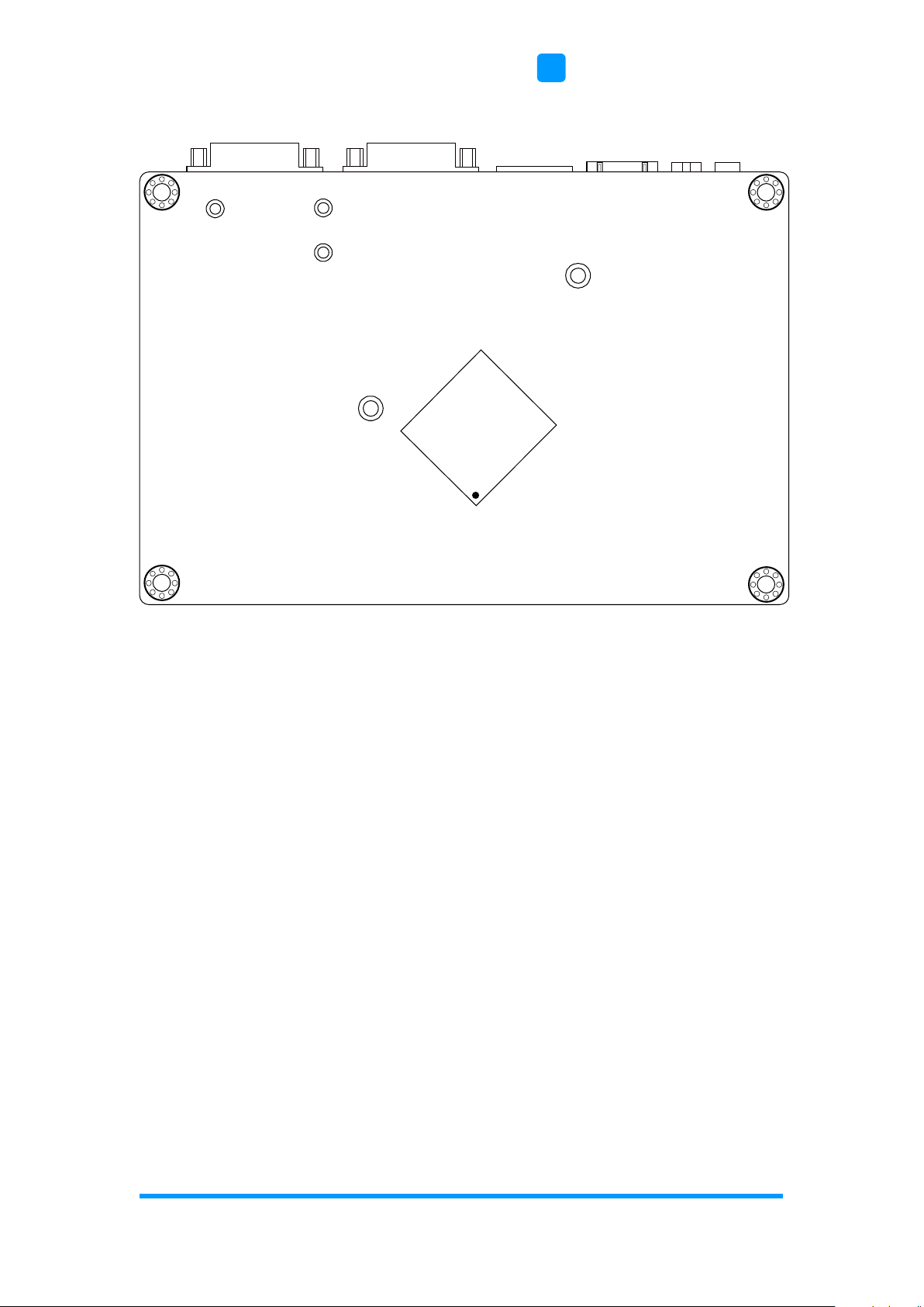
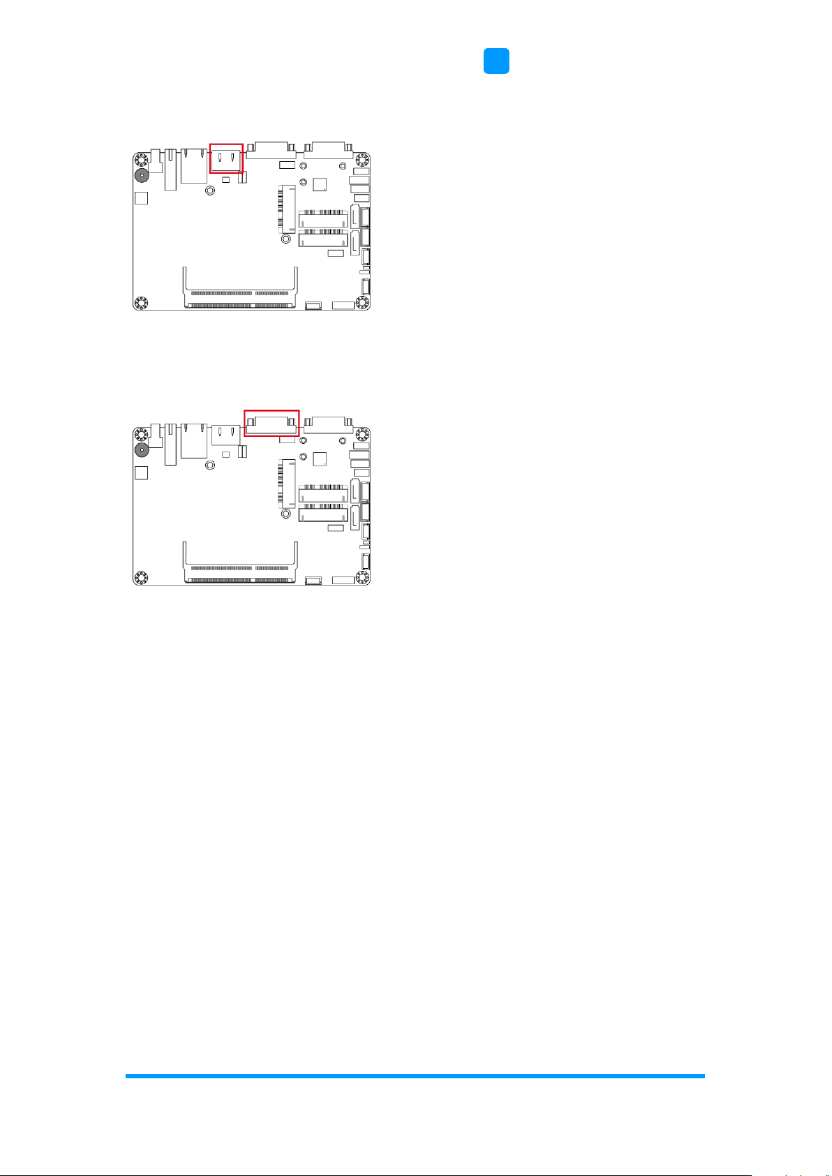
2.3 Jumper & Connector Locations on Motherboard
Motherboard: IB898
IB898 - top
BZ1
J15
J14
J4
2 72
203737471
204
1
J17
1
J16
J11
J10
J7
JP2
JP1
J3
J12
J9
J8
J1J2
J18
J19
J21
9
2
1
9
10
2
1
12
11
1
2
10
9 1
2
1
1
1
1
1
SIO
J13
J22
1
1
1
9
10
2
1
7
28
1
1 1
JP5
J20
CN4 CN1 CN3
CN5
CN6 CN7
JP4
7
2 8
1
Hardware Configuration
CSB200-898 User Manual
23
2
IB898 - bottom
Intel
®
Atom™
E3825
Dual-Core

24
CSB200-898 User Manual
2.4 Jumpers Quick Reference
Function
Connector Name
Page
LVDS Panel Power Selection
JP1
24
LVDS Panel Brightness Control Selection
JP2
25
CMOS Data Clearance
JP4
25
ME Register Clearance
JP5
26
2.4.1 LVDS Panel Power Selection (JP1)
Function
Pin closed
Illustration
3.3V
(default)
1-2
5V
2-3
1
1
1

Hardware Configuration
CSB200-898 User Manual
25
2
2.4.2 LVDS Panel Brightness Control Selection (JP2)
Function
Pin closed
Illustration
3.3V
Open
5V
(default)
Close
2.4.3 CMOS Data Clearance (JP4)
Function
Pin closed
Illustration
Normal
(default)
1-2
Clear CMOS
2-3
1
1
1
1
1
1

26
CSB200-898 User Manual
2.4.4 ME Register Clearance (JP5)
Function
Pin closed
Illustration
Normal
(default)
1-2
Clear ME
Register
2-3
1
1
1

Hardware Configuration
CSB200-898 User Manual
27
2
2.5 Connectors Quick Reference
Function
Connector Name
Page
USB 2.0 Port
CN4
28
USB 3.0 Port
CN1
28
LAN Port (GbE)
CN3
28
Display Port
CN5
29
VGA Port
CN6
29
COM1 Port
CN7
30
Audio Connector
J1
31
Amplifier Connector
J3
31
DDR3L SO-DIMM Socket
J4
32
LCD Backlight Connector
J7
32
SATA II / mSATA Port
J9
32
SATA II Port
J12
33
SATA HDD Power Connector
J10, J11
33
Full-Size Mini-PCIe Connector
J13
33
Full-Size Mini-PCIe / mSATA Connector
J14
34
Half-Size Mini-PCIe Connector
J15
34
Front Panel Setting Connector
J16
34
Motherboard Power Input Connector
J17
35
COM2 (RS-232) Port
J18
35
Digital I/O Connector
J19
36
USB 2.0 Connector
J22
36
Factory Use Only
J2, J8, J21
--

28
CSB200-898 User Manual
2.5.1 USB 2.0 Port (CN4)
2.5.2 USB 3.0 Port (CN1)
2.5.3 LAN Port (GbE) (CN3)
Hardware Configuration
CSB200-898 User Manual
29
2
2.5.4 Display Port (CN5)
2.5.5 VGA Port (CN6)

30
CSB200-898 User Manual
2.5.6 COM1 RS-232/422/485 Port (CN7)
COM1 port is jumper-less and configurable in BIOS.
Pin
Assigment
Pin
Assigment
1
DCD, Data carrier detect
6
DSR, Data set ready
2
RXD, Receive data
7
RTS, Request to send
3
TXD, Transmit data
8
CTS, Clear to send
4
DTR, Data terminal ready
9
RI, Ring indicator
5
GND, ground
Pin
Assignment
RS-232
RS-422
RS-485
1
DCD
TX-
DATA-
2
RX
TX+
DATA+
3
TX
RX+
NC
4
DTR
RX-
NC
5
Ground
Ground
Ground
6
DSR
NC
NC
7
RTS
NC
NC
8
CTS
NC
NC
9
RI
NC
NC
1
6
5
9

Hardware Configuration
CSB200-898 User Manual
31
2
2.5.7 Audio Connector (J1)
Pin
Assigment
Pin
Assigment
1
Lineout_L
7
JD_Linein
2
Lineout_R
8
GNd
3
JD_Front
9
MIC_L
4
GND
10
MIC-R
5
Linein_L
11
JD_MIC1
6
Linein_R
12
GND
2.5.8 Amplifier Connector (J3)
Pin
Assigment
Pin
Assigment
1
OUTL+
3
OUTR-
2
OUTL-
4
OUTR+
11
12 2
1
1

32
CSB200-898 User Manual
2.5.9 DDR3L SO-DIMM Socket (J4)
2.5.10 LCD Backlight Connector (J7)
Pin
Assigment
Pin
Assigment
1
+12V(1A)
3
Brightness Control
2
Backlight Enable
4
Ground
2.5.11 SATA II / mSATA Port (J9)
1

Hardware Configuration
CSB200-898 User Manual
33
2
2.5.12 SATA II Port (J12)
2.5.13 SATA HDD Power Connector (J10, J11)
Pin
Assigment
Pin
Assigment
1
+5V (1A)
3
Ground
2
Ground
4
+12V (1A)
2.5.14 Full-Size Mini-PCIe Connector (J13)
1

34
CSB200-898 User Manual
2.5.15 Full-Size Mini-PCIe / mSATA Connector (J14)
2.5.16 Half-Size Mini-PCIe Connector (J15)
2.5.17 Front Panel Setting Connector (J16)
Pin
Assigment
Pin
Assigment
1
Power BTN
5
Reset BTN
2
Power BTN
6
Reset BTN
3
HDD LED+
7
Power LED+
4
HDD LED-
8
Power LED-
8
7 1
2

Hardware Configuration
CSB200-898 User Manual
35
2
2.5.18 Motherboard Power Input Connector (J17)
Pin
Assigment
1
VCC12
2
GND
2.5.19 COM2 RS-232 Port (J18)
Pin
Assigment
Pin
Assigment
1
DCD, Data carrier detect
6
DSR, Data set ready
2
RXD, Receive data
7
RTS, Request to send
3
TXD, Transmit data
8
CTS, Clear to send
4
Data terminal ready
9
RI, Ring indicator
5
GND, ground
10
Not Used
1
2
19
10

36
CSB200-898 User Manual
2.5.20 Digital I/O Connector (J19)
Pin
Assigment
Pin
Assigment
1
GND
6
OUT0
2
VCC(500mA)
7
IN3
3
OUT3
8
IN1
4
OUT1
9
IN2
5
OUT2
10
IN0
2.5.21 USB 2.0 Connector (J22)
Pin
Assigment
Pin
Assigment
1
VCC
5
D0+
2
GND
6
D1-
3
D0-
7
GND
4
D1+
8
VCC
1
210
9
2
1 7
8

37
Chapter 3
Driver Installation
The information provided in this chapter includes:
• Intel
®
Chipset Software Installation Utility
• Intel
®
Graphics Driver Installation
• HD Audio Driver Installation
• Intel
®
Trusted Execution Engine Installation
• USB 3.0 Driver Installaion
• LAN Driver Installation

38
CSB200-898 User Manual
3.1 Introduction
This section describes the installation procedures for software drivers. The
software drivers are in a disk enclosed with the product package. If you find
anything missing, please contact the distributor where you made the
purchase.
Note: After installing your Windows operating system, you must install the
Intel® Chipset Software Installation Utility first before proceeding with
the drivers installation.

Driver Installation
CSB200-898 User Manual
39
3
3.2 Intel® Chipset Software Installation Utility
The Intel® Chipset drivers should be installed first before the software drivers
to install INF files for Plug & Play function for the chipset components. Follow
the instructions below to complete the installation.
1. Insert the disk enclosed in the package. Click Intel and then Intel(R)
Baytrail Chipset Drivers.
2. Click Intel(R) Chipset Software Installation Utility.
3. When the Welcome screen to the Intel
®
Chipset Device Software appears,
click Next to continue.
4. Click Yes to accept the software license agreement and proceed with the
installation process.
5. The driver has been completely installed. Click Finish to restart the
computer and for changes to take effect.

40
CSB200-898 User Manual
3.3 Intel® Graphics Driver Installation
1. Insert the disk enclosed in the package. Click Intel and then Intel(R)
Baytrail Chipset Drivers.
2. Click Intel(R) Baytrail Graphics Driver.
3. When the Welcome screen appears, click Next to continue.
4. Click Yes to agree with the license agreement and continue the
installation.
5. The driver has been completely installed. Click Finish to restart the
computer and for changes to take effect.

Driver Installation
CSB200-898 User Manual
41
3
3.4 HD Audio Driver Installation
1. Insert the disk enclosed in the package with the board. Click Intel and
then Intel(R) Baytrail Chipset Drivers.
2. Click Realtek High Definition Audio Driver.
3. On the Welcome screen of the InstallShield Wizard, click Next for
installation.
4. The driver has been completely installed. Click Finish to restart the
computer and for changes to take effect.

42
CSB200-898 User Manual
3.5 Intel® Trusted Execution Engine Installation
Note: The driver is for Windows 7 only.
1. Insert the disk enclosed in the package with the board. Click Intel and
then Intel(R) Baytrail Chipset Drivers.
2. Click Intel(R) TXE Drivers.
3. When the Weocome screen appears, click Next.
4. Click Next to agree with the license agreement and continue the
installation.
5. The driver has been completely installed. Click Finish to restart the
computer and for changes to take effect.

Driver Installation
CSB200-898 User Manual
43
3
3.6 USB 3.0 Driver Installation
1. Insert the disk enclosed in the package with the board. Click Intel and
then Intel(R) Baytrail Chipset Drivers.
2. Click Intel(R) USB 3.0 Drivers.
3. On the Welcome screen of the InstallShield Wizard, click Next.
4. Click Yes to agree with the license agreement.
5. On the Readme File Information screen, click Next for installation.
6. The driver has been completely installed. Click Finish to restart the
computer and for changes to take effect.

44
CSB200-898 User Manual
3.7 LAN Driver Installation
1. Insert the disk enclosed in the package with the board. Click LAN Card on
the left pane. Then click Intel(R) LAN Controller Drivers, and Intel(R)
I21x Gigabit Network Drivers.
2. On the Welcome screen of the InstallShield Wizard, click Next.
3. Click Next to agree with the license agreement.
4. When the wizard is ready for installation, click Install.
5. The driver has been completely installed. Click Finish to restart the
computer and for changes to take effect.

45
Chapter 4
BIOS Setup
This chapter describes the different settings available in the AMI
BIOS that comes with the board. The topics covered in this
chapter are as follows:
• Main Settings
• Advanced Settings
• Chipset Settings
• Security Settings
• Book Settings
• Save & Exit

46
CSB200-898 User Manual
4.1 Introduction
The BIOS (Basic Input/Output System) installed in the ROM of your computer
system supports Intel® processors. The BIOS provides critical low-level
support for standard devices such as disk drives, serial ports and parallel
ports. It also provides password protection as well as special support for
detailed fine-tuning of the chipset controlling the entire system.
4.2 BIOS Setup
The BIOS provides a Setup utility program for specifying the system
configurations and settings. The BIOS ROM of the system stores the Setup
utility. When you turn on the computer, the BIOS is immediately activated.
Press the <Del> key immediately allows you to enter the Setup utility. If you
are a little bit late pressing the <Del> key, POST (Power On Self Test) will
continue with its test routines, thus preventing you from invoking the Setup.
If you still need to enter Setup, restart the system by pressing the ”Reset”
button or simultaneously pressing the <Ctrl>, <Alt> and <Delete> keys.
You can also restart by turning the system Off and back On again.
The following message will appear on the screen:
Press <DEL> to Enter Setup
In general, press the arrow keys to highlight items, <Enter> to select, the
<PgUp> and <PgDn> keys to change entries, <F1> for help, and <Esc> to
quit.
When you enter the BIOS Setup utility, the Main Menu screen will appear on
the screen. The Main Menu allows you to select from various setup functions
and exit choices.
Warning: It is strongly recommended that you avoid making any changes to
the chipset defaults.
These defaults have been carefully chosen by both AMI and your
system manufacturer to provide the absolute maximum
performance and reliability. Changing the defaults could make the
system unstable and crash in some cases.

BIOS Setup
CSB200-898 User Manual
47
4
4.3 Main Settings
BIOS Setting
Description
System Date
Sets the date.
Use the <Tab> key to switch between the data
elements.
System Time
Set the time.
Use the <Tab> key to switch between the data
elements.

48
CSB200-898 User Manual
4.4 Advanced Settings
This section allows you to configure, improve your system and allows you to
set up some system features according to your preference.
BIOS Setting
Description
OnBoard LAN PXE Rom
Enables or disables the execution of UEFI and
Legacy PXE OpROM.

BIOS Setup
CSB200-898 User Manual
49
4
4.4.1 ACPI Settings
BIOS Setting
Description
Enable ACPI Auto
Configuration
Enables / Disables the ACPI Auto
configuration.
Enable Hibernation
Enables / Disables the system ability to
hibernate (OS/S4 Sleep State). This option
may not be effective with some OS.
ACPI Sleep State
Selects a ACPI sleep state for the system to
enter.
Options:
• Suspend Disabled
• S3 (Suspend to RAM)

50
CSB200-898 User Manual
4.4.2 iSMART Controller

BIOS Setup
CSB200-898 User Manual
51
4
BIOS Setting
Description
Power-On after Power
failure
Enables / Disables the system to be turned on
automatically after a power failure.
Power Resume Delay
Enables / Disables to delay the time for system
to turn on.
Power Resume Delay
Value (Seconds)
Sets the delay timer for the system to resume
power if power failure occurs.
The minimum delay timer is 5 seconds, and the
maximum is 255 seconds.
Temperature Guardian
Generate the reset signal when system hands
up on POST.
Schedule Slot 1 / 2
Sets up the hour / minute / day for the poweron schedule for the system.
Options:
• None
• Power On
• Power On / Off

52
CSB200-898 User Manual
4.4.3 Super IO Configuration
BIOS Setting
Description
Serial Port Configuration
Sets Parameters of Serial Ports.
You can enable / disable the serial port and
select an optimal settings for the Super IO
device.

BIOS Setup
CSB200-898 User Manual
53
4
4.4.3.1. Serial Port 1 Configuration
BIOS Setting
Description
Change Settings
Selects an optimal settings for the Super I/O
device.
Options:
• Auto
• IO=3F8h ; IRQ=4
• IO=3F8h ; IRQ=3, 4, 5, 6, 7, 9. 10, 11, 12
• IO=2F8h ; IRQ=3, 4, 5, 6, 7, 9. 10, 11, 12
• IO=3E8h ; IRQ=3, 4, 5, 6, 7, 9. 10, 11, 12
• IO=2E8h ; IRQ=3, 4, 5, 6, 7, 9. 10, 11, 12
Device Mode
Changes the mode of serial port.
Options:
• RS232 Enable
• RS485 Enable
• RS422 Enable

54
CSB200-898 User Manual
4.4.3.2. Serial Port 2 Configuration
BIOS Setting
Description
Change Settings
Selects an optimal settings for the Super I/O
device.
Options:
• Auto
• IO=3E8h ; IRQ=3
• IO=3E8h ; IRQ=3, 4, 5, 6, 7, 9. 10, 11, 12
• IO=2E8h ; IRQ=3, 4, 5, 6, 7, 9. 10, 11, 12
• IO=2F0h ; IRQ=3, 4, 5, 6, 7, 9. 10, 11, 12
• IO=2E0h ; IRQ=3, 4, 5, 6, 7, 9. 10, 11, 12

BIOS Setup
CSB200-898 User Manual
55
4
4.4.4 Hardware Monitor
BIOS Setting
Description
CPU Shutdown
Temperature
This field enables or disables the Shutdown
Temperature
Options:
• Disabled
• 70 ℃
• 75 ℃
• 80 ℃
• 85 ℃
• 90 ℃
• 95 ℃

56
CSB200-898 User Manual
4.4.5 CPU Configuration
BIOS Setting
Description
Socket 0 CPU Information
Displays the specific socket CPU Information.

BIOS Setup
CSB200-898 User Manual
57
4
4.4.6 IDE Configuration
BIOS Setting
Description
Serial-ATA (SATA)
Enables / Disables the Serial ATA.
SATA Speed Support
Supports SATA speed Gen.1 or Gen. 2.
SATA Mode
Selects IDE / AHCI Mode.
Serial –ATA Port 0
Enables / Disables Serial Port 0.
SATA Port0 HotPlug
Enables / Disables SATA Port 0 HotPlug.
Serial –ATA Port 1
Enables / Disables Serial Port 1.
SATA Port1 HotPlug
Enables / Disables SATA Port 1 HotPlug.

58
CSB200-898 User Manual
4.4.7 USB Configuration
BIOS Setting
Description
Legacy USB Support
Enables / Disables Legacy USB support.
• “Auto” disables legacy support if there is no
USB device connected.
• “Disable” keeps USB devices available only
for EFI applications.
XHCI Hand-off
This is a workaround for OSes without XHCI
hand-off support. The XHCI ownership change
should be claimed by XHCI driver.
USB Mass Storage Driver
Support
Enables / Disables the support for USB mass
storage driver.
USB Transfer time-out
The time-out value for Control, Bulk, and
Interrupt transfers.
Options: 1, 5, 10, 20 sec(s)
Device reset time-out
Seconds of delaying execution of start unit
command to USB mass storage device.
Options: 10, 20, 30, 40 secs

BIOS Setup
CSB200-898 User Manual
59
4
BIOS Setting
Description
Device power-up delay
Maximum time it will take the device before the
device properly reports itself to the Host
Controller.
“Auto” uses default value: for a Root port it is
100 ms; for a Hub port, the delay is taken from
Hub descriptor.

60
CSB200-898 User Manual
4.5 Chipset Settings
4.5.1 North Bridge

BIOS Setup
CSB200-898 User Manual
61
4
4.6 Security Settings
BIOS Setting
Description
Administrator Password
Sets an administrator password for the setup
utility.
User Password
Sets a user password.

62
CSB200-898 User Manual
4.7 Boot Settings
BIOS Setting
Description
Setup Prompt Timeout
Number of seconds to wait for setup activation
key.
65535 (0xFFFF) means indefinite waiting.
Bootup NumLock State
Selects the keyboard NumLock state as On or
Off.
Quiet Boot
Enables / Disables Quiet Boot option.
Fast Boot
Enables / Disables boot with initialization of a
minimal set of devices required to launch the
active boot option. Has no effect for BBS boot
options.
Boot Option Priorities
Sets the system boot order.
Options:
• Hard Disk
• CD/DVD
• USB - Hard Disk, CD/DVD, Key, Floppy, Lan
• Network
• Disabled

BIOS Setup
CSB200-898 User Manual
63
4
BIOS Setting
Description
Hard Disk Drive BBS
Priorities
Specificies the priority sequence of the bood
devices from available hard disk drives.

64
CSB200-898 User Manual
4.8 Save & Exit Settings
BIOS Setting
Description
Save Changes and Exit
Exits system setup after saving the changes.
Discard Changes and
Exit
Exits system setup without saving any changes.
Save Changes and Reset
Resets the system after saving the changes.
Discard Changes and
Reset
Resets system setup without saving any
changes.
Save Changes
Saves changes done so far to any of the setup
options.
Discard Changes
Discards changes done so far to any of the
setup options.
Restore Defaults
Restores / Loads defaults values for all the
setup options.
Save as User Defaults
Saves the changes done so far as user defaults.
Restore User Defaults
Restores the user defaults to all the setup
options.

65
Appendix
This section provides the mapping addresses of peripheral
devices and the sample code of watchdog timer configuration.
• I/O Port Address Map
• Interrupt Request Lines (IRQ)
• Digital I/O Sample Code
• Watchdog Timer Configuration

66
CSB200-898 User Manual
A. I/O Port Address Map
Each peripheral device in the system is assigned a set of I/O port addresses
which also becomes the identity of the device. The following table lists the I/O
port addresses used.
Address
Device Description
0x00000070-0x00000077
System CMOS/real time clock
0x00000070-0x00000077
Motherboard resources
0x00000A00-0x00000A0F
Motherboard resources
0x00000290-0x0000029F
Motherboard resources
0x00000A20-0x00000A2F
Motherboard resources
0x00000A30-0x00000A3F
Motherboard resources
0x0000E070-0x0000E077
Intel(R) Pentium(R) processor N- and Jseries / Intel(R) Celeron(R) processor Nand J-series AHCI - 0F23
0x0000E060-0x0000E063
Intel(R) Pentium(R) processor N- and Jseries / Intel(R) Celeron(R) processor Nand J-series AHCI - 0F23
0x0000E050-0x0000E057
Intel(R) Pentium(R) processor N- and Jseries / Intel(R) Celeron(R) processor Nand J-series AHCI - 0F23
0x0000E040-0x0000E043
Intel(R) Pentium(R) processor N- and Jseries / Intel(R) Celeron(R) processor Nand J-series AHCI - 0F23
0x0000E020-0x0000E03F
Intel(R) Pentium(R) processor N- and Jseries / Intel(R) Celeron(R) processor Nand J-series AHCI - 0F23
0x0000D000-0x0000D01F
Ethernet Controller
0x0000D000-0x0000D01F
Intel(R) Pentium(R) processor N- and Jseries / Intel(R) Celeron(R) processor Nand J-series PCI Express - Root Port 1 0F48
0x0000002E-0x0000002F
Motherboard resources
0x0000004E-0x0000004F
Motherboard resources
0x00000061-0x00000061
Motherboard resources
0x00000063-0x00000063
Motherboard resources
0x00000065-0x00000065
Motherboard resources

Appendix
CSB200-898 User Manual
67
Address
Device Description
0x00000067-0x00000067
Motherboard resources
0x00000080-0x0000008F
Motherboard resources
0x00000092-0x00000092
Motherboard resources
0x000000B2-0x000000B3
Motherboard resources
0x00000680-0x0000069F
Motherboard resources
0x00000400-0x0000047F
Motherboard resources
0x00000500-0x000005FE
Motherboard resources
0x00000600-0x0000061F
Motherboard resources
0x0000E080-0x0000E087
Intel(R) Atom(TM) Processor E3800
Series/Intel(R) Celeron(R) Processor
N2920/J1900
0x000003B0-0x000003BB
Intel(R) Atom(TM) Processor E3800
Series/Intel(R) Celeron(R) Processor
N2920/J1900
0x000003C0-0x000003DF
Intel(R) Atom(TM) Processor E3800
Series/Intel(R) Celeron(R) Processor
N2920/J1900
0x0000E000-0x0000E01F
Intel(R) Pentium(R) processor N- and Jseries / Intel(R) Celeron(R) processor Nand J-series Platform Control Unit - SMBus
Port - 0F12
0x00000020-0x00000021
Programmable interrupt controller
0x00000024-0x00000025
Programmable interrupt controller
0x00000028-0x00000029
Programmable interrupt controller
0x0000002C-0x0000002D
Programmable interrupt controller
0x00000030-0x00000031
Programmable interrupt controller
0x00000034-0x00000035
Programmable interrupt controller
0x00000038-0x00000039
Programmable interrupt controller
0x0000003C-0x0000003D
Programmable interrupt controller
0x000000A0-0x000000A1
Programmable interrupt controller
0x000000A4-0x000000A5
Programmable interrupt controller
0x000000A8-0x000000A9
Programmable interrupt controller
0x000000AC-0x000000AD
Programmable interrupt controller
0x000000B0-0x000000B1
Programmable interrupt controller

68
CSB200-898 User Manual
Address
Device Description
0x000000B4-0x000000B5
Programmable interrupt controller
0x000000B8-0x000000B9
Programmable interrupt controller
0x000000BC-0x000000BD
Programmable interrupt controller
0x000004D0-0x000004D1
Programmable interrupt controller
0x00000040-0x00000043
System timer
0x00000050-0x00000053
System timer
0x000003F8-0x000003FF
Serial port #1 (COM1)
0x000003E8-0x000003EF
Serial port #2 (COM2)
0x00000000-0x0000006F
PCI bus
0x00000078-0x00000CF7
PCI bus
0x00000D00-0x0000FFFF
PCI bus

Appendix
CSB200-898 User Manual
69
B. Interrupt Request Lines (IRQ)
Peripheral devices use interrupt request lines to notify CPU for the service
required. The following table shows the IRQ used by the devices on board.
Level
Function
IRQ 0
System Timer
IRQ 3
Serial Port #2 (COM2)
IRQ 4
Serial Port #1 (COM1)
IRQ 8
High precision event timer
IRQ 11
Ethernet Controller
IRQ 11
Intel(R) Pentium(R) processor N-series and J-series /
Intel(R) Celeron(R) processor N- and J-series Platform
Control Unit - SMBus Port - 0F12
IRQ 19
Intel(R) Pentium(R) processor N-series and J-series /
Intel(R) Celeron(R) processor N-series and J-series
AHCI - 0F23
IRQ 19
Intel(R) Pentium(R) processor N-series and J-series /
Intel(R) Celeron(R) processor N-series and J-series
PCI Express - Root Port 4 - 0F4E
IRQ 16
Intel(R) Pentium(R) processor N-series and J-series /
Intel(R) Celeron(R) processor N- and J-series PCI
Express - Root Port 1 - 0F48
IRQ 17
Intel(R) Pentium(R) processor N-series and J-series /
Intel(R) Celeron(R) processor N- and J-series PCI
Express - Root Port 2 - 0F4A
IRQ 18
Intel(R) Pentium(R) processor N-series and J-series /
Intel(R) Celeron(R) processor N-series and J-series
PCI Express - Root Port 3 - 0F4C
IRQ 22
High Definition Audio Controller
IRQ 81 - IRQ 190
Microsoft ACPI-Compliant System
IRQ 4294967292
Intel(R) Trusted Execution Engine Interface
IRQ 4294967293
Intel(R) USB 3.0 Extensible Host Controller
IRQ 4294967294
Intel(R) Atom(TM) Processor E3800 Series/Intel(R)
Celeron(R) Processor N2920/J1900

70
CSB200-898 User Manual
C. Digital I/O Sample Code
1. The file NCT5523D.H
//--------------------------------------------------------------------------// THIS CODE AND INFORMATION IS PROVIDED "AS IS" WITHOUT WARRANTY OF ANY
// KIND, EITHER EXPRESSED OR IMPLIED, INCLUDING BUT NOT LIMITED TO THE
// IMPLIED WARRANTIES OF MERCHANTABILITY AND/OR FITNESS FOR A
PARTICULAR
// PURPOSE.
//--------------------------------------------------------------------------#ifndef __NCT5523D_H
#define __NCT5523D_H 1
//--------------------------------------------------------------------------#define NCT5523D_INDEX_PORT (NCT5523D_BASE)
#define NCT5523D_DATA_PORT (NCT5523D_BASE+1)
//--------------------------------------------------------------------------#define NCT5523D_REG_LD 0x07
//--------------------------------------------------------------------------#define NCT5523D_UNLOCK 0x87
#define NCT5523D_LOCK 0xAA
//--------------------------------------------------------------------------unsigned int Init_NCT5523D(void);
void Set_NCT5523D_LD( unsigned char);
void Set_NCT5523D_Reg( unsigned char, unsigned char);
unsigned char Get_NCT5523D_Reg( unsigned char);
//--------------------------------------------------------------------------#endif //__NCT5523D_H

Appendix
CSB200-898 User Manual
71
2. The file MAIN.CPP
//--------------------------------------------------------------------------// THIS CODE AND INFORMATION IS PROVIDED "AS IS" WITHOUT WARRANTY OF ANY
// KIND, EITHER EXPRESSED OR IMPLIED, INCLUDING BUT NOT LIMITED TO THE
// IMPLIED WARRANTIES OF MERCHANTABILITY AND/OR FITNESS FOR A
PARTICULAR
// PURPOSE.
//--------------------------------------------------------------------------#include <dos.h>
#include <conio.h>
#include <stdio.h>
#include <stdlib.h>
#include "NCT5523D.H"
//--------------------------------------------------------------------------int main (void);
void Dio5Initial(void);
void Dio5SetOutput(unsigned char);
unsigned char Dio5GetInput(void);
void Dio5SetDirection(unsigned char);
unsigned char Dio5GetDirection(void);
//--------------------------------------------------------------------------int main (void)
{
char SIO;
SIO = Init_NCT5523D();
if (SIO == 0)
{
printf("Can not detect Nuvoton NCT5523D, program abort.\n");
return(1);
}
Dio5Initial();
//for GPIO20..27
Dio5SetDirection(0x0F); //GP20..23 = input, GP24..27=output
printf("Current DIO direction = 0x%X\n", Dio5GetDirection());
printf("Current DIO status = 0x%X\n", Dio5GetInput());
printf("Set DIO output to high\n");
Dio5SetOutput(0x0F);
printf("Set DIO output to low\n");
Dio5SetOutput(0x00);
return 0;
}
//---------------------------------------------------------------------------

72
CSB200-898 User Manual
void Dio5Initial(void)
{
unsigned char ucBuf;
ucBuf = Get_NCT5523D_Reg(0x1C);
ucBuf &= ~0x02;
Set_NCT5523D_Reg(0x1C, ucBuf);
Set_NCT5523D_LD(0x07); //switch to logic device 7
//enable the GP2 group
ucBuf = Get_NCT5523D_Reg(0x30);
ucBuf |= 0x04;
Set_NCT5523D_Reg(0x30, ucBuf);
}
//--------------------------------------------------------------------------void Dio5SetOutput(unsigned char NewData)
{
Set_NCT5523D_LD(0x07); //switch to logic device 7
Set_NCT5523D_Reg(0xE1, NewData);
}
//--------------------------------------------------------------------------unsigned char Dio5GetInput(void)
{
unsigned char result;
Set_NCT5523D_LD(0x07); //switch to logic device 7
result = Get_NCT5523D_Reg(0xE1);
return (result);
}
//--------------------------------------------------------------------------void Dio5SetDirection(unsigned char NewData)
{
//NewData : 1 for input, 0 for output
Set_NCT5523D_LD(0x07); //switch to logic device 7
Set_NCT5523D_Reg(0xE8, NewData);
}
//--------------------------------------------------------------------------unsigned char Dio5GetDirection(void)
{
unsigned char result;
Set_NCT5523D_LD(0x07); //switch to logic device 7
result = Get_NCT5523D_Reg(0xE8);
return (result);
}
//---------------------------------------------------------------------------

Appendix
CSB200-898 User Manual
73
3. The file NCT5523D.CPP
//--------------------------------------------------------------------------// THIS CODE AND INFORMATION IS PROVIDED "AS IS" WITHOUT WARRANTY OF ANY
// KIND, EITHER EXPRESSED OR IMPLIED, INCLUDING BUT NOT LIMITED TO THE
// IMPLIED WARRANTIES OF MERCHANTABILITY AND/OR FITNESS FOR A
PARTICULAR
// PURPOSE.
//--------------------------------------------------------------------------#include "NCT5523D.H"
#include <dos.h>
//--------------------------------------------------------------------------unsigned int NCT5523D_BASE;
void Unlock_NCT5523D (void);
void Lock_NCT5523D (void);
//--------------------------------------------------------------------------unsigned int Init_NCT5523D(void)
{
unsigned int result;
unsigned char ucDid;
NCT5523D_BASE = 0x4E;
result = NCT5523D_BASE;
ucDid = Get_NCT5523D_Reg(0x20);
if (ucDid == 0xC4) //NCT5523D??
{ goto Init_Finish; }
NCT5523D_BASE = 0x2E;
result = NCT5523D_BASE;
ucDid = Get_NCT5523D_Reg(0x20);
if (ucDid == 0xC4) //NCT5523D??
{ goto Init_Finish; }
NCT5523D_BASE = 0x00;
result = NCT5523D_BASE;
Init_Finish:
return (result);
}
//--------------------------------------------------------------------------void Unlock_NCT5523D (void)
{
outportb(NCT5523D_INDEX_PORT, NCT5523D_UNLOCK);
outportb(NCT5523D_INDEX_PORT, NCT5523D_UNLOCK);
}
//--------------------------------------------------------------------------void Lock_NCT5523D (void)
{
outportb(NCT5523D_INDEX_PORT, NCT5523D_LOCK);
}
//---------------------------------------------------------------------------

74
CSB200-898 User Manual
void Set_NCT5523D_LD( unsigned char LD)
{
Unlock_NCT5523D();
outportb(NCT5523D_INDEX_PORT, NCT5523D_REG_LD);
outportb(NCT5523D_DATA_PORT, LD);
Lock_NCT5523D();
}
//--------------------------------------------------------------------------void Set_NCT5523D_Reg( unsigned char REG, unsigned char DATA)
{
Unlock_NCT5523D();
outportb(NCT5523D_INDEX_PORT, REG);
outportb(NCT5523D_DATA_PORT, DATA);
Lock_NCT5523D();
}
//--------------------------------------------------------------------------unsigned char Get_NCT5523D_Reg(unsigned char REG)
{
unsigned char Result;
Unlock_NCT5523D();
outportb(NCT5523D_INDEX_PORT, REG);
Result = inportb(NCT5523D_DATA_PORT);
Lock_NCT5523D();
return Result;
}
//---------------------------------------------------------------------------

Appendix
CSB200-898 User Manual
75
D. Watchdog Timer Configuration
The Watchdog Timer (WDT) is used to generate a variety of output signals
after a user programmable count. The WDT is suitable for the use in the
prevention of system lock-up, such as when software becomes trapped in a
deadlock. Under these sorts of circumstances, the timer will count to zero and
the selected outputs will be driven.
Under normal circumstance, you will need to restart the WDT at regular
intervals before the timer counts to zero.
1. Sample Code: The file NCT5523D.H
//--------------------------------------------------------------------------//
// THIS CODE AND INFORMATION IS PROVIDED "AS IS" WITHOUT WARRANTY OF ANY
// KIND, EITHER EXPRESSED OR IMPLIED, INCLUDING BUT NOT LIMITED TO THE
// IMPLIED WARRANTIES OF MERCHANTABILITY AND/OR FITNESS FOR A
PARTICULAR
// PURPOSE.
//
//--------------------------------------------------------------------------#ifndef __NCT5523D_H
#define __NCT5523D_H 1
//--------------------------------------------------------------------------#define NCT5523D_INDEX_PORT (NCT5523D_BASE)
#define NCT5523D_DATA_PORT (NCT5523D_BASE+1)
//--------------------------------------------------------------------------#define NCT5523D_REG_LD 0x07
//--------------------------------------------------------------------------#define NCT5523D_UNLOCK 0x87
#define NCT5523D_LOCK 0xAA
//--------------------------------------------------------------------------unsigned int Init_NCT5523D(void);
void Set_NCT5523D_LD( unsigned char);
void Set_NCT5523D_Reg( unsigned char, unsigned char);
unsigned char Get_NCT5523D_Reg( unsigned char);
//--------------------------------------------------------------------------#endif //__NCT5523D_H

76
CSB200-898 User Manual
2. Sample Code: The file MAIN.CPP
//--------------------------------------------------------------------------//
// THIS CODE AND INFORMATION IS PROVIDED "AS IS" WITHOUT WARRANTY OF ANY
// KIND, EITHER EXPRESSED OR IMPLIED, INCLUDING BUT NOT LIMITED TO THE
// IMPLIED WARRANTIES OF MERCHANTABILITY AND/OR FITNESS FOR A
PARTICULAR
// PURPOSE.
//
//--------------------------------------------------------------------------#include <dos.h>
#include <conio.h>
#include <stdio.h>
#include <stdlib.h>
#include "NCT5523D.H"
//--------------------------------------------------------------------------int main (void);
void WDTInitial(void);
void WDTEnable(unsigned char);
void WDTDisable(void);
//--------------------------------------------------------------------------int main (void)
{
char SIO;
SIO = Init_NCT5523D();
if (SIO == 0)
{
printf("Can not detect Nuvoton NCT5523D, program abort.\n");
return(1);
}
WDTInitial();
WDTEnable(10);
WDTDisable();
return 0;
}
//--------------------------------------------------------------------------void WDTInitial(void)
{
unsigned char bBuf;
Set_NCT5523D_LD(0x08); //switch to logic device 8
bBuf = Get_NCT5523D_Reg(0x30);
bBuf &= (~0x01);
Set_NCT5523D_Reg(0x30, bBuf); //Enable WDTO
}
//---------------------------------------------------------------------------

Appendix
CSB200-898 User Manual
77
void WDTEnable(unsigned char NewInterval)
{
unsigned char bBuf;
Set_NCT5523D_LD(0x08); //switch to logic device 8
Set_NCT5523D_Reg(0x30, 0x01); //enable timer
bBuf = Get_NCT5523D_Reg(0xF0);
bBuf &= (~0x08);
Set_NCT5523D_Reg(0xF0, bBuf); //count mode is second
Set_NCT5523D_Reg(0xF1, NewInterval); //set timer
}
//--------------------------------------------------------------------------void WDTDisable(void)
{
Set_NCT5523D_LD(0x08); //switch to logic device 8
Set_NCT5523D_Reg(0xF1, 0x00); //clear watchdog timer
Set_NCT5523D_Reg(0x30, 0x00); //watchdog disabled
}
//---------------------------------------------------------------------------

78
CSB200-898 User Manual
3. Sample Code: The file NCT5523D.CPP
//--------------------------------------------------------------------------//
// THIS CODE AND INFORMATION IS PROVIDED "AS IS" WITHOUT WARRANTY OF ANY
// KIND, EITHER EXPRESSED OR IMPLIED, INCLUDING BUT NOT LIMITED TO THE
// IMPLIED WARRANTIES OF MERCHANTABILITY AND/OR FITNESS FOR A
PARTICULAR
// PURPOSE.
//
//--------------------------------------------------------------------------#include "NCT5523D.H"
#include <dos.h>
//--------------------------------------------------------------------------unsigned int NCT5523D_BASE;
void Unlock_NCT5523D (void);
void Lock_NCT5523D (void);
//--------------------------------------------------------------------------unsigned int Init_NCT5523D(void)
{
unsigned int result;
unsigned char ucDid;
NCT5523D_BASE = 0x4E;
result = NCT5523D_BASE;
ucDid = Get_NCT5523D_Reg(0x20);
if (ucDid == 0xC4) //NCT5523D??
{ goto Init_Finish; }
NCT5523D_BASE = 0x2E;
result = NCT5523D_BASE;
ucDid = Get_NCT5523D_Reg(0x20);
if (ucDid == 0xC4) //NCT5523D??
{ goto Init_Finish; }
NCT5523D_BASE = 0x00;
result = NCT5523D_BASE;
Init_Finish:
return (result);
}
//--------------------------------------------------------------------------void Unlock_NCT5523D (void)
{
outportb(NCT5523D_INDEX_PORT, NCT5523D_UNLOCK);
outportb(NCT5523D_INDEX_PORT, NCT5523D_UNLOCK);
}
//---------------------------------------------------------------------------

Appendix
CSB200-898 User Manual
79
void Lock_NCT5523D (void)
{
outportb(NCT5523D_INDEX_PORT, NCT5523D_LOCK);
}
//--------------------------------------------------------------------------void Set_NCT5523D_LD( unsigned char LD)
{
Unlock_NCT5523D();
outportb(NCT5523D_INDEX_PORT, NCT5523D_REG_LD);
outportb(NCT5523D_DATA_PORT, LD);
Lock_NCT5523D();
}
//--------------------------------------------------------------------------void Set_NCT5523D_Reg( unsigned char REG, unsigned char DATA)
{
Unlock_NCT5523D();
outportb(NCT5523D_INDEX_PORT, REG);
outportb(NCT5523D_DATA_PORT, DATA);
Lock_NCT5523D();
}
//--------------------------------------------------------------------------unsigned char Get_NCT5523D_Reg(unsigned char REG)
{
unsigned char Result;
Unlock_NCT5523D();
outportb(NCT5523D_INDEX_PORT, REG);
Result = inportb(NCT5523D_DATA_PORT);
Lock_NCT5523D();
return Result;
}
//-----------------------------------------------------------------------
 Loading...