

Page 1

MI912
Intel ® CoreTM 2 Duo/
Celeron GME965
Mini-ITX Motherboard
USER’S MANUAL
Version 1.0A
Page 2

Acknowledgments
Award is a registered trademark of Award Software International,
Inc.
PS/2 is a trademark of International Business Machines
Corporation.
Intel and Intel Core 2 Duo and Intel Celeron processors are
registered trademarks of Intel Corporation.
Microsoft Windows is a registered trademark of Microsoft
Corporation.
Winbond is a registered trademark of Winbond Electronics
Corporation.
All other product names or trademarks are properties of their
respective owners.
ii
MI912 User’s Manual
Page 3

Table of Contents
Introduction ...................................................... 1
Product Description ............................................................ 1
Checklist ............................................................................. 2
MI912 Specifications ......................................................... 3
Board Dimensions .............................................................. 4
Installations ...................................................... 5
Installing the CPU .............................................................. 6
Installing the Memory......................................................... 7
Setting the Jumpers............................................................. 8
Connectors on MI912 ....................................................... 12
BIOS Setup.......................................................27
Drivers Installation ......................................49
Intel Chipset Software Installation Utility ......................... 50
VGA Drivers Installation .................................................. 52
AC97 Codec Audio Driver Installation ............................ 54
LAN Drivers Installation .................................................. 55
Appendix ...........................................................59
A. I/O Port Add ress Map .................................................. 59
B. Interrupt Request Lines (IRQ) ...................................... 60
C. Watchd og Timer Configuration ................................... 61
IMPORTANT NOT E: Wh en t he syst em boots without th e CRT being
connected, there will be no image on screen when you insert the
CRT/VGA cable. To show th e image on screen, the hotkey m ust be
pressed (CTRL-ALT-F1).
MI912 User’s Manual iii
Page 4

This page is intentionally left bla nk.
iv
MI912 User’s Manual
Page 5

INTRODUCTION
Introduction
Product Description
The MI912 Mini IT X board incorporates t he Mobile Intel® GME965 Express
Chipset for Embedded Computing, consist ing of the Intel® GME965 Graphic
Memory Controller Hub (G MCH) and Intel® I/O Contr oller Hub (ICH8-M), an
optimized integrat ed graphics solut ion with a 533MHz and 800MHz front-side
bus. Dimensions of the board are 170mm x 170mm.
The integrated powerful 3D graphics engine, based on Intel® Graphics Media
Accelerator X3000 (Intel® GMA X3000) architecture, operates at core speeds of
up to 400 MHz. It features a low-power design, is validated with the Intel® Core 2
Duo and Intel® Celeron processors on 65nm process. With dual channel DDR2
667MHz two DIMM sockets, the board su pports up to 4GB of DDR2 system
memory.
Intel® Graphics supports a unique intelligent memory management scheme called
Dynamic Video Memory Technology (DVMT). DVMT handles diverse
applications by providing the maximum (384MB) availability of system memory
for general computer usage, while supplying additional graphics memory when a
3D-intensive application requests it. The Intel® GMA X3000 graphics
architecture also takes advantage of the high-performance Intel processor. Intel®
GMA X3000 graphics supports Dual Independent Display technology.
The main features of the board are:
Supports Inte l® CoreTM 2 Duo (Merom 800MHz), Intel® Celeron
Supports up to 2.4GHz, 533MHz/800MHz FSB
Two DDR2 SDRAM DIMM, Max. 4GB memory
Onboard 10/100/100 and optio nal Intel 82574L Gigabit LAN
Intel® GME965 Express VGA for CRT / LVDS
2x SATA, 6x USB 2.0, 2x C OM, Watchdo g tim er, 1394
1x Mini PCI, 1x P CI, 1xPCI-E(x1) slots, optional DVI
Optional daughter cards:
ID390: Chrontel 7308, supports 24 bit single or dual LVDS channel
ID390C: Chro ntel 7021, supports CRT
ID391: Chrontel 7307C, single DVI (connector on cable)
ID391D: Chrontel 7307C, dual DVI (connector on cable)
ID392D: Chrontel 7307C, dual DVI (one connector on card and one on cable)
MI912E/M I912EL only
MI912 User’s Manual 1
Page 6

INTRODUCTION
Checklist
Your MI912 package should include the items listed below.
• The MI912 Mini-ITX motherboard
• This User’s Manual
• 1 C D containing chipset drivers and f lash memo ry utility
• Cable k it (IDE, S erial por t, Serial AT A )
2
MI912 User’s Manual
Page 7

CPU Supported
Intel® CoreTM 2 Duo, Intel® Celeron mobile processors
CPU Voltage
0.700V ~ 1.5V (IMVP-6)
System Speed
Up to 2.4GHz or above
CPU FSB
533MHz/800MHz FSB
Cache
1MB/2MB/4MB
Green /APM
APM1.2
CPU Socket
mPGA 478MN Socket
Chipset
Intel® GME965 Chipset
ICH8M: 82801HBM 678-pin mBGA
BIOS
Award BIOS, supports ACPI Function
Memory
DDR2 667/533 SDRAM DIMM x2 (w/o ECC function), Max. 4GB
VGA
GMA965 built-in, supports CRT,RCA,S-VIDEO,HDTV
SDVO (Dual CH)
Through ID390 card (Chrontel 7308, 24 bit single/dual channel
Through ID391 card (Chrontel 7307C,DVI single or Dual)
LVDS LCD Panel
GME965 built-in, supports 24-bit (Type 1 only), single or dual channel
LVDS
LAN
1. ICH8M 10/100/gigabit MAC + PHY
2. Intel® 82574L Gigabit LAN controller x1 (MI912EF)
USB
ICH8M built-in USB 2.0 host controller, support 6 ports
Serial ATA Ports
ICH8M built-in SATA controller, supports 2 ports
1394
TI TSB43LV22 (dual port)
Parallel IDE
ICH8M built-in one channel Ultra DMA 33/66/100,CF Type II
Audio
ICH8M built-in Audio controller + High Definition Audio Codec ALC885 w/
7.1 channels, SPDIF-OUT
LPC I/O
W83627EHF: COM1, COM2 (RS232/RS422/RS485), Slim FDC 1.44MB,
headers)
Digital IO
4 in & 4 out
Keyboard/Mouse
Supports PS/2 Keyboard/Mouse Connector
Expansion Slots
PCI slot x1, PIC-E (x1) slot x1 and Mini PCI socket x1
Edge Connectors
PS/2 Connector x1 for keyboard/mouse
Surround Back)
Onboard Header/
40-pin box-header x1 for IDE1; 26-pin header x1 for Slim Floppy
SATA connector x2 for SATA ports
Watchdog Timer
Yes (256 segments, 0, 1, 2…255 sec/min)
System Voltage
+5V, +3.3V, +12V, -12V, 5VSB (2A)
Others
Modem Wakeup, LAN Wakeup
Board Size
170mm x 170mm (Mini ITX)
MI912 Specifications
GMCH: GME965 1299-pin Micro-FCBGA
LVDS, Chrontel 7021, CRT, RCA, S-VIDEO or HDTV)
• Intel 82566DM Nineveh 10/100/1000 (MI912E)
IrDA x1 & hardware monitor (3 thermal, 4 voltage monitor inputs, 2 fan
INTRODUCTION
Gigabit LAN1 RJ-45 + dual USB stack connector
Gigabit LAN2 RJ45 (option) + dual USB stack connector
DB9 x1 for COM 1; DB15 x1 for VGA
SPDIF-out connector x1; 1394 connector x1
RCA Jack 3x2 for Audio (Front-Out, Line-In, Mic , C enter/LFE, Surround &
Connectors
MI912 User’s Manual 3
CF Connector x1 @ solder side
10-pin headerx1 for Digital I/O; 10-pin header x1 for COM2
10-pin header x 1 for USB 5,6; 5-pin header x 1 for IrDA
DF13 connector x2 for LVDS;
10-pin header x1 for audio Line-Out & Mic
7-pin header x1 for 1394
Page 8
INTRODUCTION
[
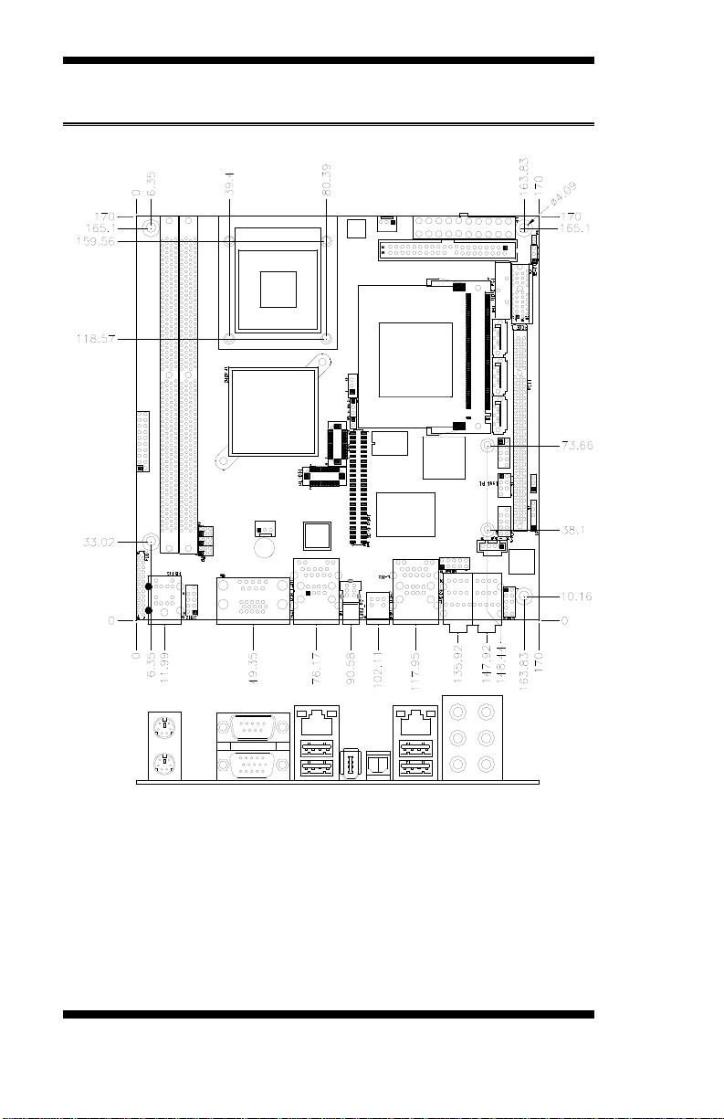
Board Dimensions
4
MI912 User’s Manual
Page 9

INSTALLATIONS
Installations
This section provides information on how to use the jumpers and
connectors on the MI912 in order to set up a workable system. The topics
covered are:
Inst alling the CPU ...................................................................... 6
Inst alling the Memory ................................................................. 7
Setting the Jumpers .................................................................... 8
Conne c to rs on MI912 ............................................................... 12
MI912 User’s Manual 5
Page 10
INSTALLATIONS
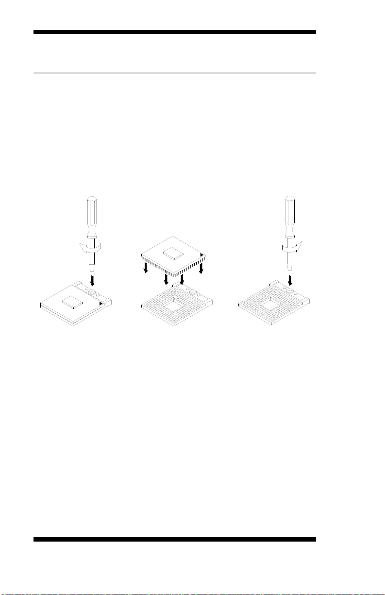
NOTE:
Ensure that the CPU heat sink and the CPU top surface are in
total contact to avoid CPU overheating problem that would
cause your system to hang or be unstable.
Installing the CPU
The MBI910 board supports a Socket 478MN (Merom) processor socket
for Intel® CoreTM 2 Duo, Intel® Ce leron mobile processors.
The processor so cket comes with a screw to secure t he processor. As
shown in the picture below, loosen the screw first before insert ing the
processor. Place the processor into the socket by making sure the notch
on the corner of the CPU corresponds with the notch on the inside of the
socket . Once the processor has slide into the sock et, fasten the screw.
6
MI912 User’s Manual
Page 11
INSTALLATIONS
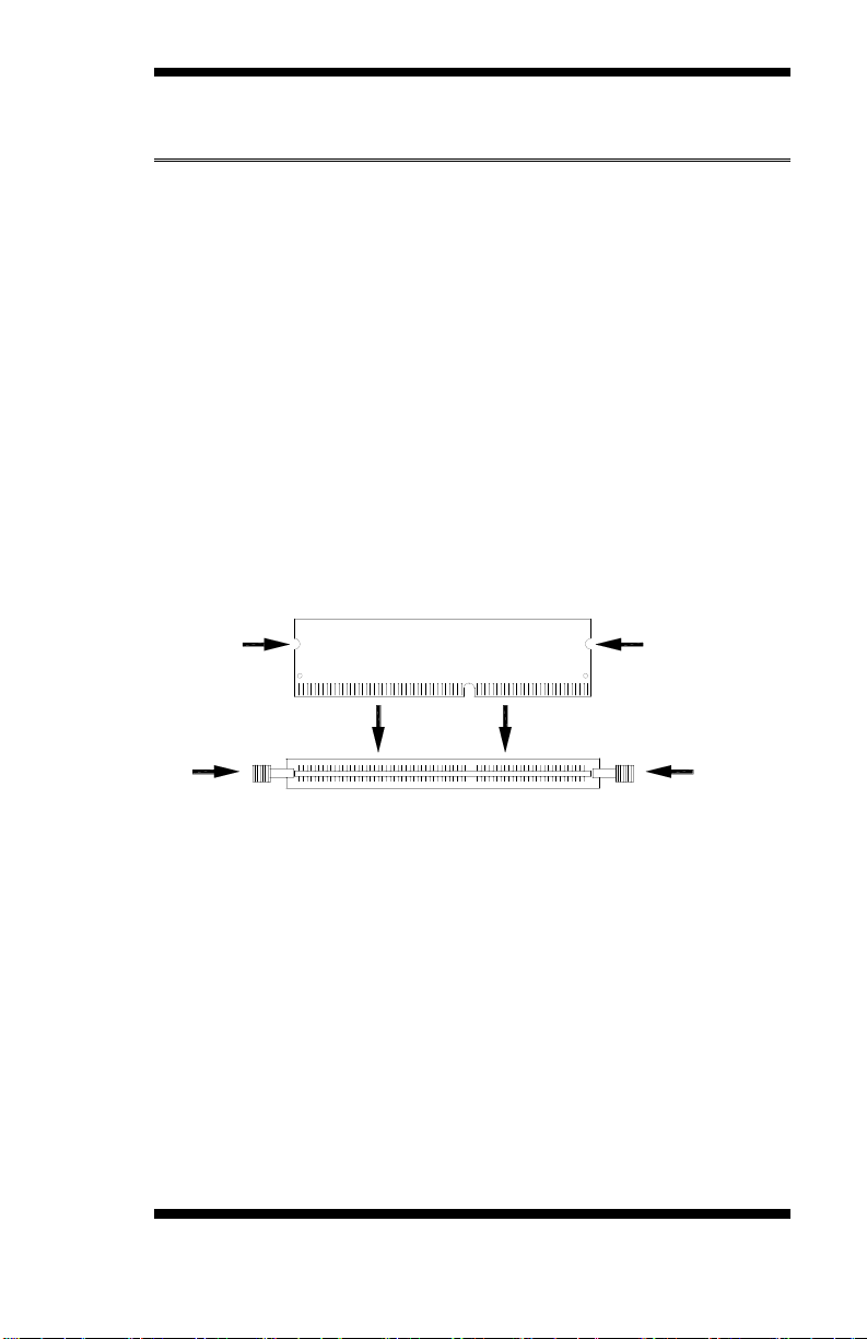
DDR2 Module
Lock
Lock
Lock Lock
Installing the Memory
The MI912 board supports two DDR2 memory sockets fo r a ma ximu m
total memory of 4GB in DDR2 memory t ype.
Installing and Removing Memory Modules
To install the DDR2 modules, locate the memory slot on the boar d and
pe rform the fo llow ing s te ps:
1. Hold the DDR2 module so that the key of the DDR2 module aligned
with that on the memory slot .
2. Gently push the DDR2 module in an uprigh t position until t he c lips of
the slot close to hold the DDR2 module in place when the DDR2
module touches the bottom of the slot.
3. To remove the DDR2 module, press the clips w ith both hands.
MI912 User’s Manual 7
Page 12

INSTALLATIONS
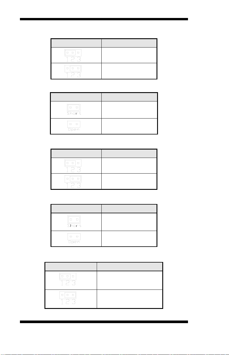
Setting the Jumpers
Jumpers are used on MI912 to select various settings and features
according to your needs and applications. Contact your supplier if you
have doubt s about the best c onfiguration for you r needs . The following
lists the connecto r s on MI912 and their respective functions.
Jumper Locations on MI912 ......................................................... 9
JBAT1: Clear CMOS Setting ...................................................... 10
JP4: CPU FSB Selection (reserved) ............................................ 10
JP5: LCD Panel Power Selection ................................................ 10
JP8: CompactFlash Slave/Master Selection ................................. 10
JP9: PCI/PCIE Riser Card Selection ........................................... 10
JP15: Keyboard/Mouse Power Selection ..................................... 11
JP17: 82574L Gigabit LAN Enable/Disable Selection.................. 11
IMPORTANT NOTE: When the system boots without the CRT being
connected, there will be no image on screen when you insert the
CRT/VGA cable. To show th e image on screen, the hotkey m ust be
pressed.
8
MI912 User’s Manual
Page 13
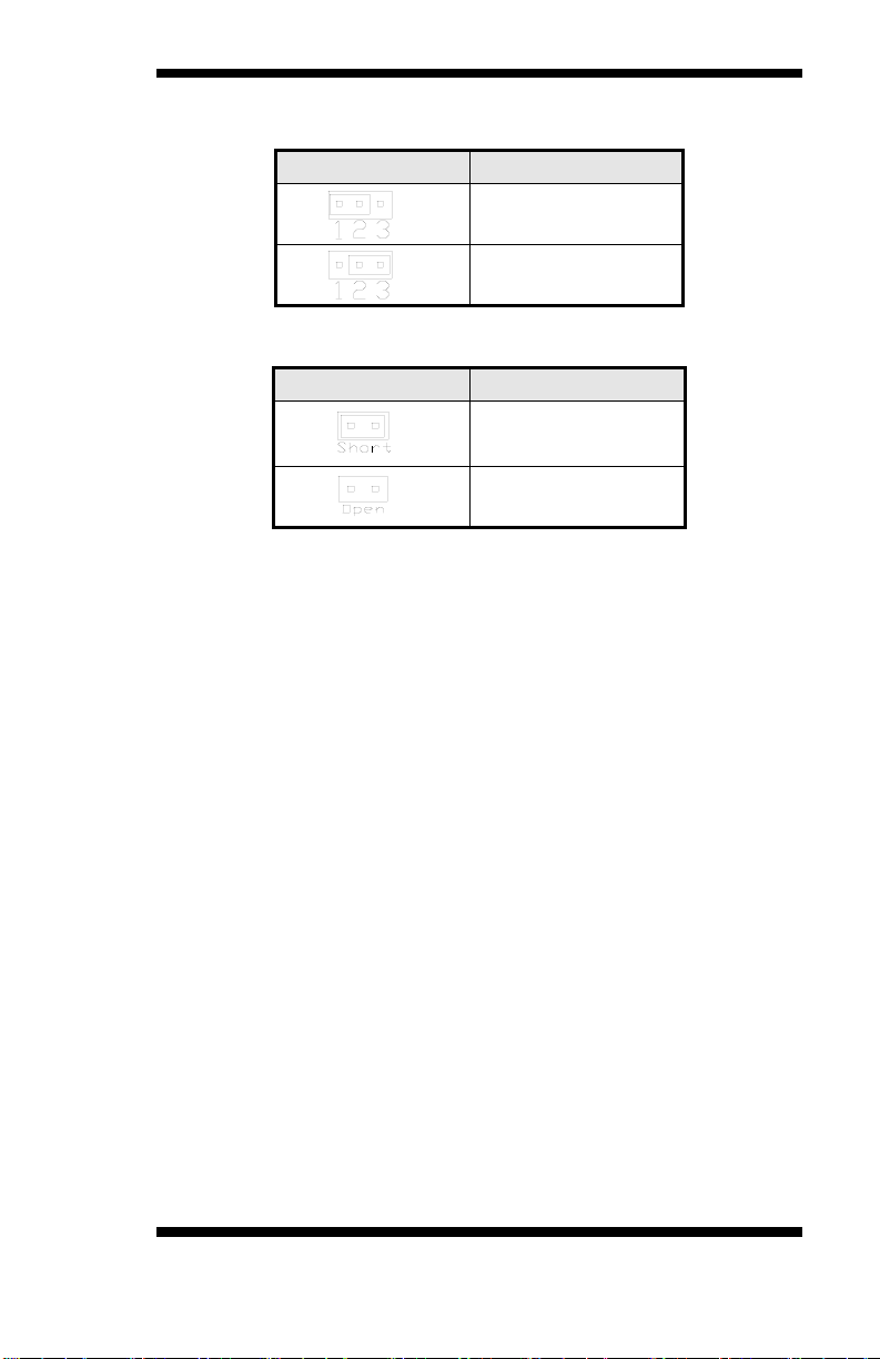
Jumper Locations on MI912
INSTALLATIONS
Jumpers on MI912 ..........................................................................Page
JP4: CPU FSB Selection ............................................................. 10
JP5: LCD Panel Power Selection ................................................ 10
JP9: PCI/P CI E Riser Card Selection ........................................... 10
JBAT1: Clear CMOS Set ting ...................................................... 10
JP8: CompactFlash Slave/Master Selection ................................. 10
MI912 User’s Manual 9
Page 14
INSTALLATIONS
JBAT1
Setting
JP4
CPU FSB
JP5
LCD Panel Power
JP8
CF Setting
JP9
Riser Card
JBAT1: Clear CMOS Setting
JP4: CPU FSB Selection (reserved)
JP5: LCD Panel Power Selection
Normal
Clear CMOS
533MHz
800MHz
3.3V
JP8: CompactFlash Slave/Master Selection
JP9: PCI/PCIE Riser Card Selection
[
10
MI912 User’s Manual
5V
Master
Slave
IP390 Riser Card
Install
IP151, IP240 Riser Card
Install
Page 15
INSTALLATIONS
JP15
KB/ MS Power
JP17
82574L GbE
JP15: Keyboard/Mouse Power Selection
+5V
5VSB
JP17: 82574L Gigabit LAN Enable/Disable Selection
Disable
Enable
MI912 User’s Manual 11
Page 16

INSTALLATIONS
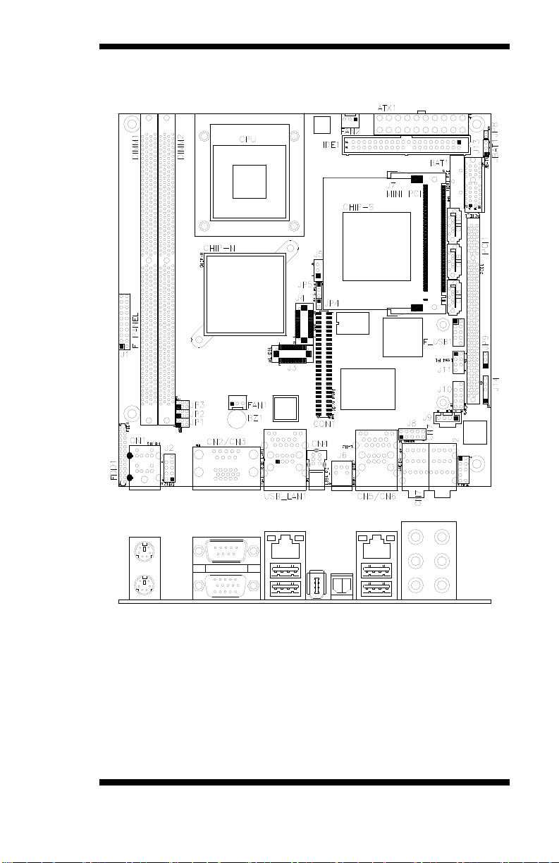
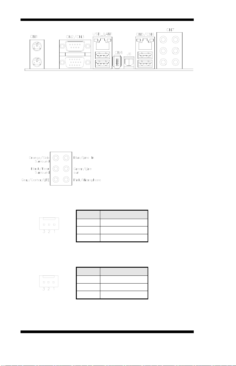
Connectors on MI912
CN1: PS/2 Keyboard and PS/2 Mouse Connectors...................... 15
CN2, CN3: COM1 and VGA Connector ..................................... 15
USB_LAN1: GbE RJ45((MI912E/MI912EF)) and USB1/2 Ports ............ 16
CN4: 1394 Connector ................................................................. 16
J6: SPDIF Out C onnector ........................................................... 16
CN5, CN6: GbE RJ-45 (MI912EF) and USB3/4 Ports ................ 16
CN7: Audio Connector ............................................................... 16
FAN1: System Fan Power Connector .......................................... 16
FAN2: CPU Fan Power Connector ............................................. 16
IDE 1: ID E Connector ................................................................. 17
FDD1: Flopp y Drive Conne c to r .................................................. 17
ATX1: ATX Power Supply Connector........................................ 18
J1 (F_PANE L ): System Function Connect or ............................... 18
F_USB1: USB0/U S B1 Connector .............................................. 20
JP1, JP2, JP3: RS232/422/485 (COM2) Selection ....................... 20
J2 : COM2 Serial Po rt ................................................................. 21
J3, J 4: LVD S Conne ctors (1st c hannel, 2nd c hannel)................... 21
J5: LCD Backlight Connector ..................................................... 21
J7: Mini PCI Connector .............................................................. 21
CN8, CN9: SATA Co nnect ors .................................................... 21
J8 : Digit al I/O ............................................................................. 22
J9: CD-In Pin Header .................................................................. 22
J10: SPI Flash Connector (factory use only) ................................ 22
J11: 1394 Connector ................................................................... 22
J12: Front Audio Connector........................................................ 22
J13: PCI-E(x1) Slot .................................................................... 22
J14: IrDA Connector .................................................................. 23
J15: Compact Flash Connector.................................................... 23
PCI1: PCI Slot (supports 2 Master) ............................................ 23
CON1: SDVO Port Co nnecto r .................................................... 23
Headers and Connectors o n Optional Daug ht er Card s ................. 24
ID390 – JP4 LCD Panel Power Selection ........................................................... 24
ID390 – J1 LCD Backlight Setting .................................................................... 24
ID390 – J3 and J2 1st/2
ID390C – J4 VGA Connector ........................................................................... 25
ID391 – J2 DVI Connector ............................................................................... 26
ID391D – J1, J2 1st/2
nd
LVDS Channel Connectors .......................................... 24
nd
DVI Connectors ............................................................ 26
12
MI912 User’s Manual
Page 17
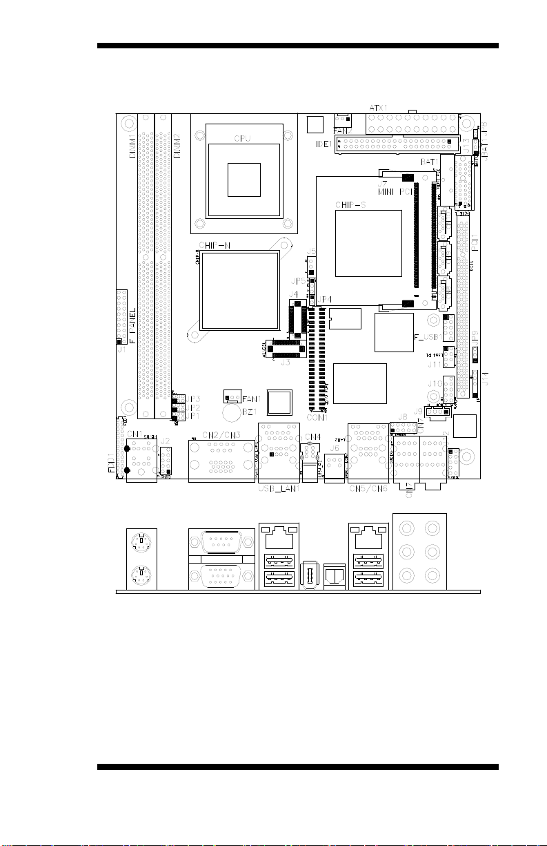
Connector Locations on MI912
INSTALLATIONS
MI912 User’s Manual 13
Page 18
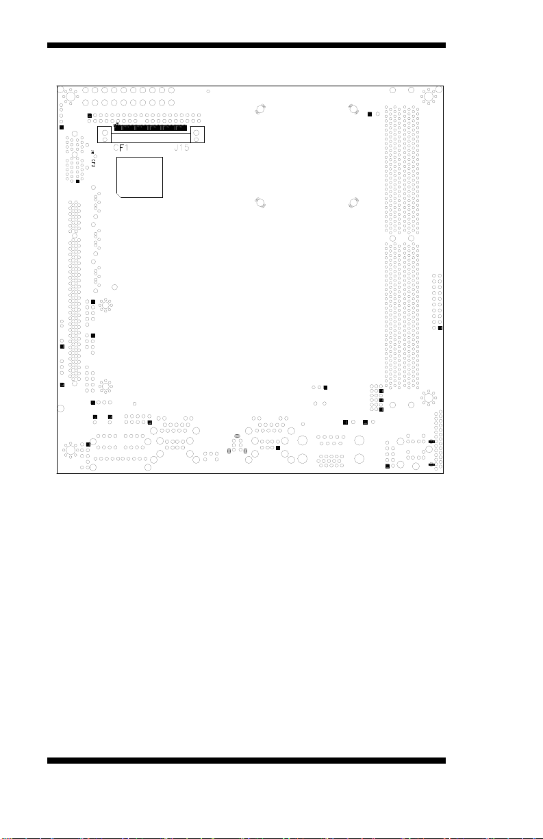
INSTALLATIONS
14
MI912 Solder Side
MI912 User’s Manual
Page 19

INSTALLATIONS
Signal Name
Keyboard
Mouse
Signal Name
Keyboard dat a
1
1
Mouse data
N.C.
2 2 N.C.
GND
3 3 GND
5V
4 4 5V
Keyboard clock
5
5
Mouse clock
N.C.
6 6 N.C.
Signal Name
Pin #
Pin #
Signal Name
DCD
1 6 DSR
RXD
2 7 RTS
TXD
3 8 CTS
DTR
4 9 RI
GND
5
10
Not Used
Signal Name
Pin #
Pin #
Signal Name
Red
1 2 Green
Blue
3 4 N.C.
GND
5 6 GND
GND
7 8 GND
N.C.
9
10
GND
N.C.
11
12
N.C.
HSYNC
13
14
VSYNC
NC
15
CN1: PS/2 Keyboard and PS/2 Mouse Connectors
PS/2 Mouse
PS/2 Keyboard
CN2, CN3: COM1 and VGA Connector
[
[[[[
MI912 User’s Manual 15
Page 20
INSTALLATIONS
Pin #
Signal Name
1
Ground
2
+12V
3
Rotat ion det ection
Pin #
Signal Name
1
Ground
2
+12V
3
Rotat ion det ection
USB_LAN1: GbE RJ45 (MI912E/MI912EF) and USB1/2 Ports
CN4: 1394 Connector
J6: SPDIF Out Connector
CN5, CN6: GbE RJ-45 (MI912EF) and USB3/4 Ports
CN7: Audio Connector
FAN1: System Fan Power Connector
FAN1 is a 3-pin header f or system fans. The fan must be a 12V (500mA).
FAN2: CPU Fan Power Connector
FAN2 is a 3-pin header for the CPU fan. The fan must be a 12V fan.
16
MI912 User’s Manual
Page 21
INSTALLATIONS
Signal Name
Pin #
Pin #
Signal Name
Reset IDE
1 2 Ground
Host data 7
3 4 Host data 8
Host data 6
5 6 Host data 9
Host data 5
7 8 Host data 10
Host data 4
9
10
Host data 11
Host data 3
11
12
Host data 12
Host data 2
13
14
Host data 13
Host data 1
15
16
Host data 14
Host data 0
17
18
Host data 15
Ground
19
20
Prot ect pin
DRQ0
21
22
Ground
Host IOW
23
24
Ground
Host IOR
25
26
Ground
IOCHRDY
27
28
Hos t ALE
DACK0
29
30
Ground
IRQ14
31
32
No connect
Address 1
33
34
No connect
Address 0
35
36
Address 2
Chip select 0
37
38
Chip se lect 1
Activity
39
40
Ground
Signal Name
Pin #
Pin #
Signal Name
VCC
1 2 INDEX
VCC
3 4 DRV_SEL
VCC
5 6 DSK_CH
NC
7 8 NC
NC
9
10
MOTOR
DINST
11
12
DIR
NC
13
14
STEP
GND
15
16
WDATA
GND
17
18
WGATE
GND
19
20
TRACK
NC
21
22
WPROT
GND
23
24
RDATA
GND
25
26
SIDE
IDE1: ID E Connector
FDD1: Floppy Drive Connector
FDD1is a slim 26-pin connector and will support up to 2.88MB FDD.
MI912 User’s Manual 17
Page 22

INSTALLATIONS
11 1
Signal Name
Pin #
Pin #
Signal Name
3.3V
11 1 3.3V
-12V
12 2 3.3V
Ground
13 3 Ground
PS-ON
14 4 +5V
Ground
15 5 Ground
Ground
16 6 +5V
Ground
17 7 Ground
-5V
18 8 Power good
+5V
19 9 5VSB
+5V
20
10
+12V
Hard Disk Drive LED
Reset Switch
Not Defined
ATX Power On Switch
Not Defined
Power LED
Pin #
Signal Name
1
Speaker out
2
No connect
3
Ground
4
+5V
ATX1: ATX Power Supply Connector
20 10
J1 (F_PANEL): System Function Connector
J1 provides connectors fo r syste m indic ators that provide light indication
of the computer activities and switches to change the computer status. J1
is a 20-p in header that provides interfaces for the following functions.
Speaker
Speaker: Pins 1 - 4
This connector provides an interface to a speaker for aud io
tone gene ration. An 8-ohm speaker is recommended.
18
MI912 User’s Manual
Page 23

Pin #
Signal Name
11
Power LED
12
No connect
13
Ground
14
No connect
15
Ground
Pin #
Signal Name
10
HDD Active
20
5V
Power LED: Pins 11 - 15
INSTALLATIONS
ATX Power ON Switch: Pins 7 and 17
This 2-pin connec tor is an “ATX Powe r Supply On/Off
Switch” on the system that connects to the power switch on
the case. When pressed, the power switch will force the
system to power on. When pressed again, it will force the
system to power off.
Reset Switch: Pins 9 and 19
The reset switch allows the user to reset the system without
turning the main power switc h off and t hen on ag ain.
Orientation is not required when making a connection to this
header.
Hard Disk Drive LED Connector: Pins 10 and 20
This connector connects to the hard drive activity LED on
contro l panel. This LED w ill f lash whe n the HDD is being
accessed.
MI912 User’s Manual 19
Page 24

INSTALLATIONS
Signal Name
Pin
Pin
Signal Name
Vcc
1 2 Vcc
D0-
3 4 D1-
D0+
5 6 D1+
Ground
7 8 Ground
NC
9
10
Ground
COM2
Function
JP3:
3-5 & 4-6
JP3:
1-3 & 2-4
JP3:
1-3 & 2-4
Pin #
Signal Name
RS-232
R2-422
RS-485
1
DCD
TX-
DATA-
2
RX
TX+
DATA+
3
TX
RX+
NC
4
DTR
RX-
NC
5
Ground
Ground
Ground
6
DSR
RTS-
NC
7
RTS
RTS+
NC
8
CTS
CTS+
NC 9 RI
CTS-
NC
10
NC
NC
NC
F_USB1: USB0/USB1 Connector
JP1, JP2, JP3: RS232/422/485 (COM2) Selection
CO M1 is f ix ed for RS-232 use only.
COM2 is selectable for RS232, RS-422 and RS-485.
The following table describes the jumper settings for COM2 selection.
RS-232 RS-422 RS-485
Jumper
Setting
(pin closed)
COM2 is jumper selectable for RS-232, RS-422 and RS-485.
1-2
JP2:
3-5 & 4-6
JP1:
3-4
JP2:
1-3 & 2-4
JP1:
5-6
JP2:
1-3 & 2-4
JP1:
20
MI912 User’s Manual
Page 25

Signal Name
Pin #
Pin #
Signal Name
DCD, Data carrier det ect
1 6 DSR, Data set r eady
RXD, Receive data
2 7 RTS, Request to send
TXD, Tran smit data
3 8 CTS, Clear to send
DTR, Data terminal ready
4 9 RI , Ring indicator
GND, ground
5
10
Not Used
Signal Name
Pin #
Pin #
Signal Name
TX0-
2 1 TX0+
Ground
4 3 Ground
TX1-
6 5 TX1+
5V/3.3V
8 7 Ground
TX3-
10 9 TX3+
TX2-
12
11
TX2+
Ground
14
13
Ground
TXC-
16
15
TXC+
5V/3.3V
18
17
ENABKL
+12V
20
19
+12V
Pin #
Signal Name
1
+12V
2
Backlight Enable
3
Ground
J2: COM2 Serial Port
INSTALLATIONS
COM2
J3, J4: LVDS Connectors (1st channel, 2nd channel)
The LVDS connectors on board consist of the first channel (J 3) and
second channel (J4).
J5: LCD Backlight Connector
J7: Mini PCI Connector
CN8, CN9: SATA Connectors
MI912 User’s Manual 21
Page 26

INSTALLATIONS
Signal Name
Pin
Pin
Signal Name
GND
1 2 VCC
OUT3
3 4 OUT1
OUT2
5 6 OUT0
IN3
7 8 IN1
IN2
9
10
IN0
Pin #
Signal Name
1
CD Audio R
2
Ground
3
Ground
4
CD Audio L
Signal Name
Pin
Pin
Signal Name
TPA+
1 2 TPB+
TPA-
3 4 TPB-
+12V
5 6 NC
GND
7 8 NC
Signal Name
Pin #
Pin #
Signal Name
MIC2_L
1 2 Ground
MIC2_R
3 4 Presence#
Line2_L
5 6 MIC2_ID
Sense
7 8 NC
Line2_R
9
10
Line2_ID
J8: Digital I/O
J9: CD-In Pin Header
J10: SPI Flash Connector (factory use only)
J11: 1394 Connector
J12: Front Audio Connector
J13: PCI-E(x1) Slot
22
MI912 User’s Manual
Page 27

Pin #
Signal Name
1
+5V
2
No connect
3
Ir RX
4
Ground
5
Ir TX
Signal Name
Pin #
Pin #
Signal Name
+12V
A1
B1
+12V
+12V
A2
B2
+12V
+5V
A3
B3
+5V
3.3V
A4
B4
3.3V
RESET
A5
B5
GND
GND
A6
B6
GND
SDVOC_CLK+
A7
B7
SDVOC_CLK-
SDVOC_Blue+
A8
B8
SDVOC_Blue-
GND
A9
B9
GND
SDVOC_Green+
A10
B10
SDVOC_Green-
SDVOC_Red+
A11
B11
SDVOC_Red-
GND
A12
B12
GND
SDVO TVClkIn+
A13
B13
SDVO TVClkIn-
SDVOB Int+
A14
B14
SDVOB Int-
GND
A15
B15
GND
SDVO CtrlData
A16
B16
SDVO CtrlClk
SDVOB Clk+
A17
B17
SDVOB Clk-
GND
A18
B18
GND
SDVOB Blue+
A19
B19
SDVOB Blue-
SDVOB Green+
A20
B20
SDVOB Green-
GND
A21
B21
GND
SDVOB Red+
A22
B22
SDVOB Red-
SDVO Stall+
A23
B23
SDVO Stall-
GND
A24
B24
GND
J14: IrDA Connector
J15: Compact Flash Connector
PCI1: PCI Slot (supports 2 Master)
CON1: SDVO Port Connector
INSTALLATIONS
MI912 User’s Manual 23
Page 28

INSTALLATIONS
JP4
Voltage
Pin #
Signal Name
1
+12V
2
Backlight Enable
3
Ground
Signal Name
Pin #
Pin #
Signal Name
TX0-
2 1 TX0+
Ground
4 3 Ground
TX1-
6 5 TX1+
5V/3.3V
8 7 Ground
TX3-
10 9 TX3+
TX2-
12
11
TX2+
Ground
14
13
Ground
TXC-
16
15
TXC+
5V/3.3V
18
17
ENABKL
+12V
20
19
+12V
Headers and Connectors on Optional Daughter Cards
ID390 – JP4 LCD Panel Powe r Selection
3.3V
5V
ID390 – J1 LCD Backlight Se t t ing
ID390 – J3 and J2 1st/2nd LVDS Channel Connec t ors
24
MI912 User’s Manual
Page 29

Signal Name
Pin #
Pin #
Signal Name
+5V
2 1 RED
Ground
4 3 GREEN
N.C.
6 5 BLUE
SDA
8 7 N.C.
HSYNC
10 9 Ground
VSYNC
12
11
Ground
SCL
14
13
Ground
N.C.
16
15
Ground
ID390C – J4 V G A Connect or
[[[[
INSTALLATIONS
MI912 User’s Manual 25
Page 30

INSTALLATIONS
Signal Name
Pin #
Pin #
Signal Name
TDC1-
2 1 TDC1+
Ground
4 3 Ground
TLC-
6 5 TLC+
+5V
8 7 Ground
NC
10 9 HPDET
TDC2-
12
11
TDC2+
Ground
14
13
Ground
TDC0-
16
15
TDC0+
NC
18
17
NC
DDC_SC
20
19
DDC_SD
Signal Name
Pin #
Pin #
Signal Name
TDC1-
2 1 TDC1+
Ground
4 3 Ground
TLC-
6 5 TLC+
+5V
8 7 Ground
NC
10 9 HPDET
TDC2-
12
11
TDC2+
Ground
14
13
Ground
TDC0-
16
15
TDC0+
NC
18
17
NC
DDC_SC
20
19
DDC_SD
ID391 – J2 DVI Connector
ID391D – J1, J2 1st/2nd DVI Connector s
Remarks: When using dual DVI, the first DVI video output is through J1. After
setting the drivers in Windows, then the second DVI output (via J2) will function.
ID391D and ID391 are diff erent since the latter (I D391) has video output via J2.
The pi n assignments of J1 a nd J2 are the same.
26
MI912 User’s Manual
Page 31

BIOS SETUP
BIOS Setup
This chapter describes the different settings available in the Award BIOS
that comes with the board. The topics covered in this chapter are as
follows:
BIOS Introduction ...................................................................... 28
BIOS Setup ................................................................................ 28
Standard CMOS Set u p ................................................................ 30
Advanced BIOS Features ............................................................ 33
Advanced Chipset Features ......................................................... 36
Integrated Peripherals ................................................................. 38
Power Management Setup .......................................................... 41
PNP/PCI Configurations ............................................................. 44
PC Health Status ......................................................................... 45
Frequency/Voltage Control ......................................................... 46
Load Fail-Safe Defaults ............................................................... 47
Load Optimized Defaults ............................................................ 47
Set Supervisor/User Password .................................................... 47
Save & Exit Setup....................................................................... 47
Exit Wit hout Saving .................................................................... 47
MI912 User’s Manual 27
Page 32

BIOS SETUP
BIOS Introduction
The Award BIOS (Basic Input/Output System) installed in your
computer system’s ROM suppor ts I ntel pro cessor s. T he BIOS pro vides
critical low-level support for a st andard device such as disk drives, serial
ports and parallel ports. It also adds vi rus and password protection as well
as special support for detailed fine-tuning o f the chip set co ntr olling the
entire system.
BIOS Setup
The Award BIOS provides a Setup utility program for specifying the
system configurations and settings. The BIOS RO M of the system store s
the Setup utility. When you turn on the computer, the Award BIOS is
im mediately activ ated. Pressing the <Del> key immediately allows y ou to
enter the Setu p ut ility. If you are a little bit late p ressing the <Del> key,
POST (Power On Self Test) will continue wit h its test routines, thus
preventing you from invoking the Setup. If you still wish to enter Setup,
restart the system by pressing the ”Reset” button or simultaneously
pressing the <Ctrl>, <Alt> and <Delete> keys. You can also restart by
turning the system Off and back On again. The following message will
appear on the screen:
Press <DEL> to Enter Setup
In general, you press the arrow keys to highli gh t items, <Enter> to select,
the <PgUp> and <PgDn> keys to change entries, <F1> for help and
<Esc> to quit.
When you enter the Set u p utility, the Main Menu screen will appear on
the screen. The Main Menu allows you to select from various setup
functions and exit choices.
28
MI912 User’s Manual
Page 33

BIOS SETUP
Advanced BIOS Features
Load Fail-Safe Defaults
Advanced Chipset Features
Load Optimized Defaults
Integrated Peripherals
Set Supervisor Password
Power Management Setup
Set User Password
PC Health Status
Exit Without Saving
F10 : Save & Exit Setup Time, Date, Hard Disk Type…
Note:
If the system cannot boot after making and saving system
with Setup, the Award BIOS supports an override to
the CMOS settings that resets your system to its default.
Warning:
It is strongly recommended that you avoid making any
manufacturer to provide the absolute maximum performance
and reliability. Changing the defaults could cause the system
Phoenix - AwardBIOS CMOS S etup Utility
Standard CMOS Features Frequency/Voltage Control
PnP/PCI Configurations Save & Exit Setup
ESC : Quit : Select Item
The section below the setup items of the Main Menu displays the control
ke ys for this menu. At the bo ttom of the Main Menu jus t below the
contro l keys section, there is another section, which displays information
on the curren tly highlig hted item in the list.
changes
changes to the chipset defaults. These defaults have been
carefully chosen by both Award and your system
to become unstable and crash in some cases.
MI912 User’s Manual 29
Page 34

BIOS SETUP
Date (mm:dd:yy)
Wed, Apr 28, 2007
Item Help
Time (hh:mm:ss)
00 : 00 : 00
Menu Level >
IDE Channel 0 Master
None
Change the day, month,
IDE Channel 0 Slave
None
IDE Channel 1 Master
None
IDE Channel 1 Slave
None
Drive A
1.44M, 3.5 in.
Drive B
None
Video
EGA/VGA
Base Memory
640K
Extended Memory
129024K
Total Memory
130048K
Standard CMOS Setup
“Standard CMOS Setup” cho ice allows you to record some basic
hardware configurations in your computer system and set the system
clock and error handling. If the motherboard is already installed in a
working s yst em, you w ill not need to s elect this option. You will n eed t o
run the Standard CMO S opt ion, however, if you change your system
hardware configurations, the onboard batter y fails, or t he configuration
stored in the CMOS memory was lost or d amaged.
Halt On No Errors
Phoenix - AwardBIOS CMOS Se tup Utility
Standard CMOS Features
Year and century
At the bottom of the menu are the control keys for use on this menu. If
you need any help in each item field, you can press the <F1> key. It will
display the relevant information to help you. The memory display at the
lower right-hand side of the m enu i s read-only. It will adjust automatically
according to t he memory changed. The following describes each item of
this menu.
Date
The date forma t is:
Day : Sun to Sat
Month : 1 to 12
Date : 1 to 31
Year : 1999 to 2099
30
MI912 User’s Manual
Page 35

BIOS SETUP
360KB
5.25 in.
1.2MB
5.25 in.
720KB
3.5 in.
1.44MB
3.5 in.
2.88MB
3.5 in.
To set the date, highli ght the “Date” fi eld an d use the PageUp/ PageDown
or +/- keys to set the current t ime.
Time
The time format is: Hour : 00 to 23
Minute : 00 to 59
Second : 00 to 59
To set the time, highlight the “Time” field and use the <PgUp>/ <PgDn>
or +/- keys to set the current t ime.
IDE Channel Master/Slave
The onboard PCI IDE connector provides Primary and Secondary
channels fo r connecting up to two IDE hard disks or ot her ID E devices.
Press <Enter> t o configure the hard disk. The selections include Auto,
Manual, and None. Select ‘Manual’ to define the drive information
manually. You will be asked to en ter the f ollowin g items.
CYLS : Number of cylinders
HEAD : Number of read/write heads
PRECOMP : Write precompensation
LANDING ZONE : Landing zone
SECTOR : Number of sectors
The Access Mode selections are as follows:
CHS (HD < 528MB)
LBA (HD > 528MB and supports
Logical Block Addressing)
Large (for MS-DOS only)
Auto
Remarks: The main board supports tw o serial ATA ports and are
represented in this setting as IDE Channel 0.
Drive A / Drive B
These fields identify the types of floppy disk drive A or drive B t ha t ha s
been installed in the computer. The available specifications are:
MI912 User’s Manual 31
Page 36

BIOS SETUP
No errors
The sys tem boot will not be halted for any error
that may be detected.
All errors
Whenever the BIOS det ects a non-fatal error,
the syst em will stop and you will be prompted.
All, But Keyboar d
The system boot will not be halted for a
keyboard error; it will stop for all other errors
All, But D iskette
The syste m boo t w ill not be halt ed fo r a d isk
error; it will stop for all other errors.
All, But D isk/Key
The syst em boot will not be halted for a keybo ard or disk error; it w ill st op for all othe rs.
Video
This field selects the type of video display card installed in your system.
You can choos e the following video displa y cards:
EGA/VGA For EGA, VGA, SEGA, SVGA
or PGA monitor adapter s. ( Default)
C GA 40 Power up in 40 column mode.
C GA 80 Power up in 80 column mode.
MONO For Hercules or MDA adapters.
Halt On
This field d et ermin es wh ethe r or not th e syst em will ha lt if an erro r is
detected during power up.
32
MI912 User’s Manual
Page 37

BIOS SETUP
CPU Feature
Press Enter
ITEM HELP
Hard Disk Boot Priority
Press Enter
Virus Warning
Disabled
Menu Level >
USB Hard Disk Boot First
Disabled
CPU L3 Cache
Enabled
Quick Power On Self Test
Enabled
First Boot Device
Hard Disk
Second Boot Device
CDROM
Third Boot Device
LS120
Boot Other Device
Enabled
Swap Floppy Drive
Disabled
Boot Up Floppy Seek
Disabled
Boot Up Num Lo ck St atus
On
Gate A20 Option
Fast
Typematic Rate Setting
Disabled
Typematic Rate (Chars/Sec)
6
Typematic Delay (Msec)
250
Security Option
Setup
APIC Mode
Enabled
MPS Version Control fo r O S
1.4
OS Select For DRAM>64MB
Non-OS2
Report No FDD For WI N 95
No
Small Logo (EPA) Show
Disabled
Advanced BIOS Features
This section allows you to configure and improve your system and allows
you to set u p some system features according to your preference.
Phoenix - AwardBIO S CM OS Setup Ut ility
Advanced BIOS Features
CPU Feature
Press Enter to configure the settings relevant to CPU Feature.
Hard Disk Boot Priority
With the field, there is the option to choose, aside from the har d dis ks connected,
“Bootable add-in Cards” which refers to other external devices.
Virus Warning
If this option is enabled, an alarm message will be displayed when trying to write
on the boot sector or on the part ition table on the disk, which is typical of the
virus.
CPU L1 and L2 Cache
Cache memory is additional memory that is faster than conventional DRAM
(system memory). CPUs from 486-type on up contain internal cache memory , and
most, but not all, modern PCs have additional (external) cache memory. When the
CPU re qu e sts d ata , th e system tr an sfers the re qu e ste d data fro m the ma i n DR A M
into cache memory, for even faster access by the CPU. These allow you to enable
(speed up memory access) or disable the cache function.
MI912 User’s Manual 33
Page 38

BIOS SETUP
Quick Power On Self Test
When enabled, this field speeds up the Power On Self Test ( P OS T ) after
the s yste m is tur n e d on . If it is s e t to Enabled, BIOS will skip some items.
First/Second/Third Boot Device
These fields determine the drive that the system searches first for an
operating system. The options available include Floppy, LS120, Hard
Disk, CDROM, ZIP100, USB-Floppy, USB-ZIP, USB-CDROM, LAN
and Disable.
Boot Other Device
These fields allow the system to search for an OS from other devices
other t han the ones selected in the First/Second/Third Boot Device.
Swap Floppy Drive
This i tem allows you to determine wh ether or not to enable Swap Floppy
Drive. When enabled, the BIOS swaps floppy drive assignments so that
Drive A b ecomes Dri ve B, an d Driv e B becom es Driv e A . By def aul t, this
field is set to Disabled.
Boot Up Floppy Seek
This feature contro ls whether the BIOS checks for a floppy dr ive while
booting up. If it cannot detect one (either due t o improper configuration
or its absence), it will flash an error message.
Boot Up NumLock Status
This al lows you to activate the NumLock function after you power up the
system.
Gate A20 Option
This field allows you to select how Gat e A20 is worked. Gate A20 is a
device used to address memory above 1 MB.
Typematic Rate Setting
When dis able d, co ntinua lly holding down a key on you r k eyboard will
generate only one instance. When enab led, you can set the two typem ati c
controls list ed n ext. By default, this field is set to Disabled.
Typematic Rate (Chars/Sec)
When the typematic rate is enabled, the system registers repeated
keystrokes speeds. Set tings are from 6 to 30 characters per second.
34
MI912 User’s Manual
Page 39

BIOS SETUP
Typematic Delay (Msec)
When the typematic rate is enabled, this item allows you to set the t ime
interval f or displ ayi ng the f irst and second characters. By defaul t, this item
is set to 250msec.
Security Option
This field allows you to limit access to the System and Setup. The default
value is Setup. When you select System, the system prompts for the User
Password every time you boot up. When you select Setup, t he system
always boots up and prompts for the Supervisor Password only when the
Se tup utility is called up.
APIC Mode
APIC stands for Advanced Programmable Interrupt Controller. The
de f ault set ting is Enabled.
MPS Version Control for OS
This o ption is spec ifies the MP S ( Multiproce ssor Specification) v ersio n
for your o p e r a ting system. MPS version 1.4 added ext ended
config uration tables to improve suppor t for multiple PCI bus
configurations and improve future expandability. The default sett ing is
1.4.
OS Select for DRAM > 64MB
This option allows the system to access greater t han 64MB of DRAM
memory when used with OS/2 that depends on certain BIOS calls to
access memory. The default setting is Non-OS/2.
Report No FDD For WIN 95
If you are using Windows 95/98 without a floppy disk drive, select
Enabled to release IRQ6. This is required to pass Windows 95/98's SCT
tes t. Y ou should also disable t he Onboard FDC C ont roller in t he
Integrated P er ipherals screen when there's no floppy drive in the system.
If you set this feature to Disabled, the BIOS will not repo rt t h e missing
floppy drive to Win95/98.
Small Logo (EPA) Show
The EPA logo appears at the right side of the monitor screen when the
syste m is boot up. Th e default setting is Disabled.
MI912 User’s Manual 35
Page 40

BIOS SETUP
System BIOS Cache able
Enabled
ITEM HELP
Memory Hole at 15M-16M
Disabled
PCI Express Roo t Port Func
Press Enter
** VGA S etting **
PEG/On Chip VGA Co ntrol
Auto
PEG Force X1
Disabled
On-Chip Frame Buffer Size
8MB
DVMT Mode
DVMT
DVMT/FIXED me mory Size
128MB
SDVO De v ic e Setting
None SDVO LVDS Protocol
1CH 18bit
SDVO Panel Number
852x480
Boot Dis play
CRT
Panel Scaling
Auto Panel Number
1024x768 18 bit SC
LAN PXE Option ROM
All Disable
Advanced Chipset Features
This Setup menu controls the configuration of the chipset.
System BIOS Cacheable
The setting of Enabled allows caching of the system BIOS ROM at
F000h-FFFFFh, resulting in better system performance. However, if any
program writes to this memory area, a system error may result.
Video BIOS Cacheable
The Setting Enabled allows caching of the video BIOS ROM at
C0000h-F7FFFh, resulting i n better video performance. However, if any
program writes to this memory area, a system error may result.
Memory Hole At 15M-16M
In order t o improve performance, certain space in memory can be
reserved for ISA cards. This memory must be mapped into the memory
space below 16 MB. The choices are Enabled and Disabled.
Phoenix - Awa rdBIOS CMOS Setup Utility
Advanced Chipset Features
36
MI912 User’s Manual
Page 41

BIOS SETUP
640x480
18bit SC
800x480
18bit SC
800x600
18bit SC
1024x768
18bit SC
1280x1024
18bit DC
1280x768
18bit SC
1400x1050
18bit DC
1600x1200
18bit DC
On-Chip VGA Setting
The fields under the On-Chip VGA Setting and their default settings are:
PEG/On Chip VGA Control: Auto
On-Chip Frame Buffer Size: 8MB
DVMT Mode: DVTM
DVMT/Fixed Memory Size: 128MB
SDVO Device Setting: (LVDS, DVI, Dual DVI, CRT)
Remarks: Set to LVDS for ID390, Set to CRT to ID390C, Set to DVI for
ID391/ID392/ID391D/ID392D
SDVO LVDS Protocol: 1Ch SPWG, 18bit
SDVO Panel Number: 1024x768
Boot Display: CRT+LVDS
Panel Scaling: Auto
Panel Number: 1024x768 18 bit SC
Panel Scaling
The default setting is Auto. T he op tions available include On and Off.
Panel Number
These fields allow you to select the LCD Panel type. The default values
for these port s ar e:
LAN PXE Option ROM
The default setting is All Disable.
MI912 User’s Manual 37
Page 42

BIOS SETUP
OnChip IDE Device
Press Enter
ITEM HELP
SuperIO Device
Press Enter
Menu Level >
USB Device Setting
Press Enter
IDE HDD Block Mode
Enabled
ITEM HELP
IDE DMA transfe r access
Enabled
Menu Level >
***On-Chip Seria l ATA Se tting***
SATA Mode
IDE
On-Chip Serial A T
Combined Mode
***On-Chip PATA S etting***
On-chip Primary PCI IDE
Enabled
IDE Primary Master PIO
Auto
IDE Primary Slave PIO
Auto
IDE Primary Master UDMA
Auto
IDE Primary Slave UDMA
Auto
On-Chip Secondar y P CI IDE
Enabled
IDE Secondary Mast er PIO
Auto
IDE Secondary Slave PIO
Auto
IDE Secondary Mast er UDMA
Auto
IDE Secondary Slave UDMA
Auto
POWER ON Function
BUTTON ONLY
ITEM HELP
KB Power ON Passw ord
Enter Hot Key power ON
Ctrl-F1
Onboard Serial Port 1
3F8/IRQ4
Menu Level >
Onboard Serial Port 2
2F8/IRQ3
UART Mode Select
Normal
RxD, TxD Active
Hi, Lo
IR Transm is s ion Delay
Disabled
UR2 Duplex Mode
Half
Use IR P ins
IR-Rx2Tx2
PWRON After PWR-Fail
Off
Integrated Peripherals
This section sets configurations for your hard disk and other integrat ed
peripherals. T he first screen shows three main items for user to select.
Once an item selected, a submenu appears. Details follow.
Phoenix - AwardBIOS CMOS Se tup Utility
Inte gr ated Peripherals
Phoenix - AwardBIOS CMOS Se tup Utility
OnChip IDE Device
Phoenix - AwardBIOS CMOS Se tup Utility
SuperIO Devi ce
38
MI912 User’s Manual
Page 43

BIOS SETUP
USB 1.0 Contr oller
Enabled
ITEM HELP
USB 2.0 Controller
Enabled
USB Keyboard Function
Enabled
USB Mouse Function
Enabled
Menu Level >
USB Storage Function
Enabled
*** USB Mass St orage Device Boot Se tting ***
Phoenix - AwardBIOS CMOS Se tup Utility
USB Device Setti ng
IDE HDD Block Mode
This f ie ld a llow s yo ur ha rd disk c ontr oller to use the fast block mode to
transfer data to and from your hard disk drive.
IDE DMA transfer access
This field, by default, is enabled
On-chip Primary PCI IDE Enabled
This field, by default, is enabled
On-chip Primary/Secondary PCI IDE
The integrated peripheral controller contains an IDE interface with
support for two I DE channels. Select Enabled to activate each channel
separately.
IDE Primary/Secondary Master/Slave PIO
These fi el ds allow y our system h ard dis k controller to work faster. Rather
than have the BIOS issue a series of commands that transfer to or from
the disk drive, PIO (Programmed Input/Output) allows the BIOS to
communicate with the controller and CPU directly.
The system supports five modes, numbered from 0 (default) to 4, which
primarily differ in timing. When Auto is selected, the BIOS will select the
best available mode.
IDE Prim ary /Secondary Master /Slav e UDMA
These fields allow your system to improve disk I/O throughput to
33Mb/sec with the Ultra DMA/33 feature. The options are Auto and
Disabled.
On-Chip Serial ATA Setting
The fields under the SATA setting include Ser ial ATA Mode (IDE) and
ON-Chip Serial AT (Combin ed Mode).
MI912 User’s Manual 39
Page 44

BIOS SETUP
Power ON Function
This f ie ld is related to how the system is powered on – s uch a s wit h t he
use of convent ional po wer but to n, ke yboar d or hot keys. The d efault is
BUTTON ONLY.
KB Power ON Password
This field allows users to set the password when keyb oard power on is the
mode of the Power ON function.
Hot Key Power ON
This field sets certain keys, also know n a s hot keys, on the keyboard that
can be used as a ‘switch’ t o power o n t he system.
Onboard Serial Port
These fields allow you to select the onboard serial ports and their
addresses. The default values for these ports are:
Serial Po rt 1 3F8/IRQ4
Serial Po rt 2 2F8/IRQ3
UART Mode Select
This field determines the UART 2 mode in your computer. The default
value is Normal. Other opt ions include IrDA and ASKIR.
PWRON After PWR-Fail
This field sets the system power status whether on or off when po wer
returns to the system from a power failure situat ion.
USB 1.0 Controller
The options for this field are Enabled and Disabled. B y default, this fie ld
is set to Enabled.
USB 2.0 Controller
The options for this field are Enabled and Disabled. By default, this field
is set to Enabled. In order to use USB 2.0, necessary OS drivers must be
installed first. Please update your system to Windows 2000 SP4 or
Windows XP SP2.
USB Keyboard/Mouse/Storage Function
The options for this field are Enabled and Disabled. B y default, this fie ld
is set to Enabled.
40
MI912 User’s Manual
Page 45

ACPI Function
Enabled
ITEM HELP
ACPI S us pend
S3(POS)
RUN VGA B IOS if S3 Resume
Auto
Menu Level >
Power Management
User Define
Video Off Method
DPMS
Yes
Suspend Type
Stop Grant
Modem Use IRQ
3
Suspend Mode
Disabled
HDD Powe r Down
Disabled
Soft-Off by PWR-BTTN
Instant-Off
CPU THRM-Throttling
50.0%
Wake-Up by PCI Card
Disabled
Power On by Ring
Disabled
USB KB Wake-Up From S3
Disabled
Resume by Alarm
Disabled
Date (of Month) Alarm
0
Time (hh:mm:ss) Alarm
0 : 0 : 0
** Reload Global Time r E v ents **
Primary IDE 0
Disabled
Primary IDE 1
Disabled
Secondary IDE 0
Disabled
Secondary IDE 1
Disabled
FDD, COM, LPT Port
Disabled
PCI PIRQ[A-D] #
Disabled
Min. Power Saving
Minimum power management
Max. Powe r Saving
Maximum power management.
User Define
Each of the ranges is from 1 min. to 1hr.
Power Management Setup
Video Off In S us pend
Phoenix - AwardBIOS CMOS Se tup Utility
Power Management Setup
BIOS SETUP
ACPI Function
Enable this function to support ACPI (Advance Configuration and Power
Interface).
ACPI Suspend
The default setting of the ACPI Suspend mode is S3(POS).
RUN VGABIOS if S3 Resume
The default setting of this field is Auto.
Power Management
This field allows you to select the type of power saving management
modes. There are four selections for Power Management.
MI912 User’s Manual 41
Except for HDD Power Do wn which
ranges from 1 min. t o 1 5 min.
Page 46

BIOS SETUP
Video Off Method
This field defines the Video Off features. There are t hree options.
V/H SYNC + Blank Defaul t setting, bl ank the screen an d turn off
vertical and horizontal scanning.
DPMS Allo ws BIOS to control the vide o disp lay.
Blank Screen Writes blanks to the video buffer.
Video Off In Suspend
When enabled, the vide o is off in susp end mode. The default setting is
Yes.
Suspend Type
The default setting for the Suspend Type field is Stop Grant.
Modem Use IRQ
This field sets the IRQ used by the Modem. By default, the sett ing is 3.
Suspend Mode
When enabled, and after the set time of system inactivity, all devices
except the CPU will be shut off.
HDD Power Down
When enabled, and after the set t ime of system inactivity, the hard disk
drive will be powered down while all other devices remain active.
CPU THRM-Throttling
When the system enters Doze mode, the CPU clock runs only part of the
time. You may select the percent of time that the clock runs.
Soft-Off by PWRBTN
This f ield defines the power-off mode when using an ATX power supply .
The Instant Off mode allows powering off immediately upon pressin g the
power button. In the Del ay 4 S ec mode, the system powers off when the
power button is pressed for more than four seconds or enters the suspend
mode when pressed for less than 4 seconds.
Wake up by PCI Card
By d efault , this field is disabled.
42
MI912 User’s Manual
Page 47

BIOS SETUP
Power On by Ring
This field enables or disables the power on of t he system through t he
modem connected to the serial port o r LAN.
USB KB Wake-Up From S3
This field, by de fault, is d isabled.
Resume by Alarm
This field enables or disables the resumpt ion of the sys tem o pera tion.
When enabled, the user is allowed to set t he Date and Time.
Reload Global Timer Events
The HDD, FDD, COM, LPT Ports, and PCI PIRQ are I/O events that can
prevent the system from en tering a power savi ng m ode or can awaken the
system f rom such a m ode. When an I/O device wan ts to gain the attention
of the operating system, it si gnals thi s by causing an IRQ to occur. When
the operating system i s ready to respond to the request, it interrupts itself
and performs the service.
MI912 User’s Manual 43
Page 48

BIOS SETUP
PCI Slot
ITEM HELP
Reset Configuration Data
Disabled
Menu Level
Resources Controlled By
Auto (ESCD)
IRQ Resources
Press Enter
PCI/VGA Palette Snoop
Disabled
Auto
INT Pin 2 As s ignm ent
Auto
INT Pin 3 As s ignm ent
Auto
INT Pin 4 As s ignm ent
Auto
INT Pin 5 As s ignm ent
Auto
INT Pin 6 As s ignm ent
Auto
INT Pin 7 As s ignm ent
Auto
INT Pin 8 As signment
Auto
**PCI Express relative items**
Maximum Payload Size
128
PNP/PCI Conf igurations
This option co nfigures the PCI bus system. All PCI bus systems on the
system use INT#, thus all installed PCI cards must be set to t his value.
Init Display First
INT Pin 1 As s ignm ent
Init Display First
The default setting is PCI Card.
Reset Configuration Data
This f i el d al l ows y ou to determi ne wh ether to reset the configuration data
or not . T he default value is Disabled.
Resources Controlled by
This PnP BIOS can configure all of the b oot and compatible dev ices with
the use of a PnP operat ing system such as Windows 95.
PCI/VGA Palette Snoop
Some non-standard VGA display cards may not show colors pro perly.
This f i eld al l ows y ou to set whether or not MPEG ISA/VESA VGA cards
can work with PCI/VGA. When this field is enabled, a PCI/VGA can
work with an MPEG ISA/VESA VGA card. When this fi eld is disab l ed, a
PCI/VGA cannot work with an MPEG ISA/VESA card.
Maximum P ayload Size
The default setting of the PCI Express Maximum Payload Size is 4096.
Phoenix - AwardBIOS CMOS Se tup Utility
PnP/PCI Configurat ions
Select Yes if you are
using a Plug and Play
capable operating
system Select No if
you need the BIOS to
configure non-boot
devices
44
MI912 User’s Manual
Page 49

BIOS SETUP
Shutdown Temperat ur e
Disabled
ITEM HELP
CPU Warning Temperature
Disabled
Current System Temp
45°C/113°F
Menu Level >
Current CPU Te m p
45°C/113°F
FAN1 Spe ed
5400 RPM
FAN2 Spe ed
5400 RPM
+12 V
1.32 V
V1.9
1.8V
+5V
5.25 V
-12V
-12.59
VBAT (V)
3.21 V
5VSB(V)
5.67 V
1st Smart Fan Temperat ure
Disabled
2st
Smart Fan Temperat ure
Disabled
PC Health Status
This section shows the parameters in determining the PC Health Status.
These parameters include temperatures, fan speeds and voltages.
Vcore 1.02 V
3.3V 3.37V
CPU Warning Temperature
This field allows the user to set the temperature so that when the
temperature is reached, the system sounds a warning. This function can
help prevent damage to the system that is caused by overheating.
Temperatures/Voltages
These fields are the parameters of the hardware monitoring function
feature of the motherboard. The values are read-only values as monitored
by the system and show t he PC healt h status.
Shutdown Temperature
This field allows the user to set the temperature by which the system
automatically s huts down once the threshold temperature is reached. This
function can help prevent damage to the system that is caused by
overheating.
1st 2st Smart Fan Temperature
This field enables or disables the smart fan feature. At a certain
temperature, the fan starts turning. Once the temperature drops to a
certain level, it stops turning again.
Phoenix - AwardBIO S CM OS Setup Ut ility
PC Health S tatus
MI912 User’s Manual 45
Page 50

BIOS SETUP
Auto Detect P CI Clk
Disabled
ITEM HELP
Spread Spectrum Modulated
Disabled
Menu Level >
Frequency/Voltage Control
This section shows the user how to configure the processor frequency.
Auto Detect PCI Clk
This field enables or disables the auto detection of the PCI clock.
Spread Spectrum Modulated
This field sets the value of the spread spectrum. The default setting is
Disabled. This field is for CE testing use only.
Phoenix - AwardBIOS CMOS Se tup Utility
Frequency/Voltage Control
46
MI912 User’s Manual
Page 51

BIOS SETUP
Load Fail-Safe Def aults
This option allows you to load the troubleshooting default values
permanently stored in the BIOS ROM. These default settings are
non-optimal and dis able all hig h-performance features.
Load Optimized Defaults
This option allows you to load the default values to your system
configuration. These default settings are optimal and enable all high
performance features.
Set Supervisor Passwor d
These two o pt ions set t he system passwo rd . S upe rvisor P asswo r d set s a
password that will be used to prot ect the system and Setup utility. User
Password sets a password that will b e used ex clusively on the system. To
specify a password, highlight the type you want and press <Enter>. T he
Enter P a ssword: message prompts on the screen. Type the passwor d , up
to eight characters in length, and press <Enter>. The system confirms
your password by asking you to type it again. After setting a password,
the screen automatically returns to the main screen.
To disabl e a password, just press the <Enter> key when you are prompted
to enter the password. A message will confirm the password to be
disabl ed. Once the password is di sabled, the system wi l l boot and you can
enter Setup freely.
Save & Exit Setup
This option allows you to determine whether or not to accept the
modificat ions. If you type “Y”, you will quit the setup ut ility a nd s ave all
changes into the CMOS memory. If you type “N”, you will return to
Se tup utility.
Exit Wi thout Saving
Select this optio n to exit the Setup utility without saving the changes you
hav e ma d e in this s e s s ion. Typin g “ Y ” w ill quit t h e S e tu p u tility w ithout
saving the mo dificat ions. Typin g “N ” will retu rn you to Set up ut ility.
MI912 User’s Manual 47
Page 52

BIOS SETUP
This page is intentionally left bla nk.
48
MI912 User’s Manual
Page 53

DRIVERS INSTALLATION
Drivers Installation
This section descri bes the i n stall ati on procedures for software and drivers
under the Windows 2000 and Windows XP. The software and drivers are
included w ith the motherboard. If you find the items missing, please
contact the vendor where you made the purchase. The contents of this
section inclu de the fo llow ing:
Intel Chipse t Software I nstallation Ut ility .................................. 50
VG A Drivers Insta llat ion .......................................................... 52
AC97 C odec A udio D river Insta llat ion ..................................... 54
LAN Drivers Insta llat ion ........................................................... 55
IMPORTANT NOTE:
After installing your Windows operating system (Windows 2000/ XP),
you must install first the Intel Chipset Software Installation Utility before
proceeding with the drive rs in st allation.
MI912 User’s Manual 49
Page 54

DRIVERS INSTALLATION
Intel Chipset Soft ware Insta llatio n Utility
The I ntel Chipset Drivers should be installed first before the software
drivers to enable Plug & Play INF support for I nt el chipset components.
Follow the instructions bel ow to c om plete the install ation under Wi ndows
2000/XP.
1. Insert the CD that comes with the board. Click Intel Chipsets and then
Intel(R)GM 965Chipset Drive rs.
2. Clic k Intel(R) Chipset Software Installation Utility.
3. When the Welcome screen appears, click Next t o continue.
50
MI912 User’s Manual
Page 55

DRIVERS INSTALLATION
4. C lick Yes to accept t he software license agreement and pro ceed with
the installation process.
5. On Readme Informati on screen, click Next to continue the installation.
6. The Setup pr ocess is now complete. Click Finish to restart the
computer and for changes to t ake effect.
MI912 User’s Manual 51
Page 56

DRIVERS INSTALLATION
VGA Drivers I n sta lla tio n
To ins t all the VGA drivers, follow the steps below to proceed with the
installation.
1. Insert t he CD t hat comes with the motherboard. C lick Intel Chipsets
and then Intel(R) GME965Chipset Dri ve rs.
2. Clic k Intel(R) GME965Chipset Family Graphics Driver.
3. When the Welcome screen appears, click Next to continue.
52
MI912 User’s Manual
Page 57

DRIVERS INSTALLATION
4. Click Yes to to agree with the license agreement and continue the
installation.
5. Proceed as instructed and restart the co mputer as pr ompted and for
changes to take effect.
IMPORTANT NOTE:
When you have restarted the computer, your com pu ter screen wil l b e
blank. At this point, press CTRL-ALT-F1 simultan eously, if you are
using CRT monitor. If you are using LVDS LCD panel, press
CTRL-ALT-F3. If you a re using DVI m o n i t o r, press CTRL-ALT-F4.
MI912 User’s Manual 53
Page 58

DRIVERS INSTALLATION
AC97 Codec Audio Driver Installation
Follow the steps below to install the Realtek AC97 Codec Audio Drivers.
1. Insert t he CD t hat comes with the motherboard. Click Intel Chipsets
and then Intel(R) GME965Chipset Drive rs.
2. Clic k Realtek AC'97 Codec Audio Driver.
3. Click Finish to restart the computer and for changes to t ake effect.
54
MI912 User’s Manual
Page 59

DRIVERS INSTALLATION
LAN D riv e r s In s ta llat ion
Follow th e st ep s b elo w to complete the installation of t he In t el PR O
LAN drivers.
1. Insert t he CD t hat comes with the motherboard. C lick Intel Chipsets
and then Intel(R) GME965Chipset Drive rs, then In t el ( R) PRO LAN
Network Drivers.
2. Click Install Base Software to continue.
3. When prompted, restar t the computer for new settings to take effect.
MI912 User’s Manual 55
Page 60

DRIVERS INSTALLATION
Follow the steps below to install the Intel 82574L Gigabit LAN
drivers.
1. Insert the CD that comes with the motherboard. C lick L AN Ca rd and
then Intel(R) PRO 82574L LAN Drivers.
2. Click Install Drivers and Software. When the Welcome screen
appears, click Next to c ontinu e .
3. Click Next to to agree with the license agreement.
56
MI912 User’s Manual
Page 61

DRIVERS INSTALLATION
4. Click the Drivers checkbox as sh own bel ow and cl i ck Next to continue
installation. Then, click Install to begin the installatio n.
4. When InstallShie ld Wiz ard ha s complet ed in st allation, click Finish.
MI912 User’s Manual 57
Page 62

DRIVERS INSTALLATION
This page is intentionally left bla nk.
58
MI912 User’s Manual
Page 63

APPENDIX
Address
Device Description
000h - 01Fh
DMA Controller # 1
020h - 03Fh
Interrupt Controller #1
040h - 05Fh
Timer
060h - 06Fh
Keyboard Cont r oller
070h - 07Fh
Real Time Clock, NMI
080h - 09Fh
DMA Page Register
0A0h - 0BFh
Interrupt Controller #2
0C0h - 0DFh
DMA Controller # 2
0F0h
Clear Math Coprocessor Busy Signal
0F1h
Reset Math Coprocessor
1F0h - 1F7h
IDE Interface
278 - 27F
Pa rallel Port #2(LPT2)
2F8h - 2FFh
Serial Port #2(COM2)
2B0 - 2DF
Graphics adapter Contro ller
378h - 3FFh
Pa rallel Port #1(LPT1)
360 - 36F
Network Ports
3B0 - 3BF
Monochrome & Printer adapter
3C0 - 3CF
EGA adapter
3D0 - 3DF
CGA ad apter
3F0h - 3F7h
Flopp y Disk Controlle r
3F8h - 3FFh
Serial Port #1(COM1)
Appendix
A. I/O Port Address Map
Each peripheral device in the system is assigned a set of I/O port
addresses which also becomes the identity of the device. The following
table lists the I/O port addresses used.
MI912 User’s Manual 59
Page 64

APPENDIX
Level
Function
IRQ0
Sys te m Timer Output
IRQ1
Keyboard
IRQ2
Interrupt Cascade
IRQ3
Se rial Port # 2
IRQ4
Se rial Port # 1
IRQ5
Reserved
IRQ6
Flopp y Disk Controlle r
IRQ7
Pa rallel Port #1
IRQ8
Real Time Clock
IRQ9
Reserved
IRQ10
Reserved
IRQ11
Reserved
IRQ12
PS/2 Mo u se
IRQ13
80287
IRQ14
Primary IDE
IRQ15
Secondary IDE
B. Interrupt Request Lines (IRQ)
Peripheral devi ces use i nterrupt request li nes to notify C PU for the service
required. The following table shows the IRQ used by the devices on
board.
60
MI912 User’s Manual
Page 65

APPENDIX
C. Watchdog Timer Configuration
The WDT is used to generate a variety of output signals after a user
programmable count. The WDT is suitable for use in the prevention of
syste m loc k-up, such as when software becomes trapped in a deadlock.
Under these sorts of circumstances, the timer will count to zero and the
selected outputs will be driven. Under normal circumstance, the user will
restart the WDT at regular intervals before the timer counts to zer o.
SAMPLE CODE:
//===========================================================================
//
// THIS CODE AND INFORMATION IS PROVIDED "AS IS" WITHOUT WARRANTY OF ANY
// KIND, EITHER EXPRESSED OR IMPLIED, INCLUDING BUT NOT LIMITED TO THE
// IMPLIED WARRANTIES OF MERCHANTABILITY AND/OR FITNESS FOR A PARTICULAR
// PURPOSE.
//
//===========================================================================
#include <stdio.h>
#include <stdlib.h>
#include "W627EHF.H"
//===========================================================================
int main (int argc, char *argv[]);
void copyright(void);
void EnableWDT(int);
void DisableWDT(void);
//===========================================================================
int main (int argc, char *argv[])
{
unsigned char bBuf;
unsigned char bTime;
char **endptr;
copyright();
if (argc != 2)
{
printf(" Parameter incorrect!!\n");
return 1;
}
if (Init_W627EHF() == 0)
{
printf(" Winbond 83627HF is not detected, program abort.\n");
return 1;
}
bTime = strtol (argv[1], endptr, 10);
printf("System will reset after %d seconds\n", bTime);
EnableWDT(bTime);
return 0;
}
//===========================================================================
MI912 User’s Manual 61
Page 66

APPENDIX
void copyright(void)
{
printf("\n======== Winbond 83627EHF Watch Timer Tester (AUTO DETECT) ========\n"\
" Usage : W627E_WD r eset_time\n"\
" Ex : W627E_WD 3 => reset system after 3 second\n"\
" W627E_WD 0 => disable watch dog timer\n");
}
//===========================================================================
void EnableWDT(int interval)
{
unsigned char bBuf;
bBuf = Get_W627EHF_Reg( 0x2D);
bBuf &= (!0x01);
Set_W627EHF_Reg( 0x2D, bBuf); //Enable WDTO
Set_W627EHF_LD( 0x08); //switch to logic device 8
Set_W627EHF_Reg( 0x30, 0x01); //enable timer
bBuf = Get_W627EHF_Reg( 0xF5);
bBuf &= (!0x08);
Set_W627EHF_Reg( 0xF5, bBuf); //count mode is second
Set_W627EHF_Reg( 0xF6, interval); //set timer
}
//===========================================================================
void DisableWDT(void)
{
Set_W627EHF_LD(0x08); //switch to logic device 8
Set_W627EHF_Reg(0xF6, 0x00); //clear watchdog timer
Set_W627EHF_Reg(0x30, 0x00); //watchdog disabled
}
//===========================================================================
62
MI912 User’s Manual
Page 67

APPENDIX
//===========================================================================
//
// THIS CODE AND INFORMATION IS PROVIDED "AS IS" WITHOUT WARRANTY OF ANY
// KIND, EITHER EXPRESSED OR IMPLIED, INCLUDING BUT NOT LIMITED TO THE
// IMPLIED WARRANTIES OF MERCHANTABILITY AND/OR FITNESS FOR A PARTICULAR
// PURPOSE.
//
//===========================================================================
#include "W627EHF.H"
#include <dos.h>
//===========================================================================
unsigned int W627EHF_BASE;
void Unlock_W627EHF (void);
void Lock_W627EHF (void);
//===========================================================================
unsigned int Init_W627EHF(void)
{
unsigned int result;
unsigned char ucDid;
W627EHF_BASE = 0x2E;
result = W627EHF_BASE;
ucDid = Get_W627EHF_Reg(0x20);
if (ucDid == 0x88)
{ goto Init_Finish; }
W627EHF_BASE = 0x4E;
result = W627EHF_BASE;
ucDid = Get_W627EHF_Reg(0x20);
if (ucDid == 0x88)
{ goto Init_Finish; }
W627EHF_BASE = 0x00;
result = W627EHF_BASE;
Init_Finish:
return (result);
}
//===========================================================================
void Unlock_W627EHF (void)
{
outportb(W627EHF_INDEX_PORT, W627EHF_UNLOCK);
outportb(W627EHF_INDEX_PORT, W627EHF_UNLOCK);
}
//===========================================================================
void Lock_W627EHF (void)
{
outportb(W627EHF_INDEX_PORT, W627EHF_LOCK);
}
//===========================================================================
void Set_W627EHF_LD( unsigned char LD)
{
Unlock_W627EHF();
outportb(W627EHF_INDEX_PORT, W627EHF_REG_LD);
outportb(W627EHF_DATA_PORT, LD);
Lock_W627EHF();
}
MI912 User’s Manual 63
Page 68

APPENDIX
//===========================================================================
void Set_W627EHF_Reg( unsigned char REG, unsigned char DATA)
{
Unlock_W627EHF();
outportb(W627EHF_INDEX_PORT, REG);
outportb(W627EHF_DATA_PORT, DATA);
Lock_W627EHF();
}
//===========================================================================
unsigned char Get_W627EHF_Reg(unsigned char REG)
{
unsigned char Result;
Unlock_W627EHF();
outportb(W627EHF_INDEX_PORT, REG);
Result = inportb(W627EHF_DATA_PORT);
Lock_W627EHF();
return Result;
}
//===========================================================================
//===========================================================================
//
// THIS CODE AND INFORMATION IS PROVIDED "AS IS" WITHOUT WARRANTY OF ANY
// KIND, EITHER EXPRESSED OR IMPLIED, INCLUDING BUT NOT LIMITED TO THE
// IMPLIED WARRANTIES OF MERCHANTABILITY AND/OR FITNESS FOR A PARTICULAR
// PURPOSE.
//
//===========================================================================
#ifndef __W627EHF_H
#define __W627EHF_H 1
//===========================================================================
#define W627EHF_INDEX_PORT (W627EHF_BASE)
#define W627EHF_DATA_PORT (W627EHF_BASE+1)
//===========================================================================
#define W627EHF_REG_LD 0x07
//===========================================================================
#define W627EHF_UNLOCK 0x87
#define W627EHF_LOCK 0xAA
//===========================================================================
unsigned int Init_W627EHF(void);
void Set_W627EHF_LD( unsigned char);
void Set_W627EHF_Reg( unsigned char, unsigned char);
unsigned char Get_W627EHF_Reg( unsigned char);
//===========================================================================
#endif //__W627EHF_H
64
MI912 User’s Manual
 Loading...