

Page 1

MI802
Intel® Cedar Trail + NM10
Mini-ITX Motherboard
USER’S MANUAL
Version 1.0A
Page 2

Acknowledgments
AMI BIOS is a trademark of American Megatrends Inc.
PS/2 is a trademark of International Business Machines
Corporation.
Intel and Luna-Pier are registered trademarks of Intel
Corporation.
Microsoft Windows is a registered trademark of Microsoft
Corporation.
Winbond is a registered trademark of Winbond Electronics
Corporation.
All other product names or trademarks are properties of their
respective owners.
ii
MI802 User’s Manual
Page 3

Table of Contents
Introduction ...................................................... 1
Checklist ............................................................................. 2
MI802 Specifications ......................................................... 3
Board Dimensions .............................................................. 4
Installations ...................................................... 5
Installing the Memory......................................................... 6
Setting the Jumpers............................................................. 7
Connectors on MI802 ....................................................... 12
BIOS Setup.......................................................21
Drivers Installation ......................................41
Intel Chipset Software Installation Utility ......................... 42
VGA Drivers Installation .................................................. 43
Realtek HD Audio Driver Installation .............................. 44
LAN Drivers Installation .................................................. 45
Appendix ...........................................................47
A. I/O Port Add ress Map .................................................. 47
B. Interrupt Request Lines (IRQ) ...................................... 48
C. Watchdo g Ti mer Configuration ................................... 49
D. Digital I/O Sample Cod e ............................................. 53
MI802 User’s Manual iii
Page 4

This pa ge is intent iona lly left blank .
iv
MI802 User’s Manual
Page 5

INTRODUCTION
Introduction
MI802 is a Mini ITX boar d (170 mm x 170mm) tha t comes with the Int el
Atom D2550 processor that runs 1.86GHz and has a 1M B L 2 cach e. The
board is based on the Intel® CG82NM10 PCH chipset and supports two
SODIMM for a maximum memory support of 4 GB.
MI802 features the integrated GMA3650 Int el graphics controller and
supports both CRT and DVD-D video displ ay i n terface, as wel l asa 24-bit
dual channel interface with the help of Chrontel CH7511B device.
Onboard functional connections are available for two SATA por ts, six
COM ports, eight USB 2.0 ports, audio and a PS/2 keyboard/m ouse stack
conne ctor . Ad dit iona l Exp ansion c omes in o ne slim PCI slo t, two M ini
PCI-e(x1) slots. P ower connections is with a +12~24V DC in (ATX
4-pin).
Remarks: Currently, the board comes in two versions:
MI802 – with Cedar T r ail-D / Atom D2550 1.86G TDP=10W
DDR3-1066MHz SO-DIMM x 2 (w/o ECC), Max. 4GB, Single channel
MI802N – with Cedar T r ail-M / Atom N2600 1.6G TDP=3.5W
DDR3-800MHz SO-DIMM x 1 (w/o ECC), M ax. 2GB , Single channe l
MI802 User’s Manual 1
Page 6

INTRODUCTION
Checklist
Your MI802 package should include the items listed below.
• The MI802 Mini-IT X motherboard
• This User’s Manual
• 1 C D containing chipset d rivers and flash me mor y utility
• Serial ATA cable
• I/O sh ield
2
MI802 User’s Manual
Page 7

Form Factor
Mini-ITX
CPU Type
Intel® AtomTM D2550/N2600 processor (32nm Technology)
22mm x 22mm, Micro-F CB GA 559 [TDP=10W/3/5W]
CPU Speed
1.86GHz / 1MB L2 cache (MI802)
1.6GHz / 1MB L2 cache (MI802N)
BIOS
AMI BIOS, support ACPI Func tion
Chipset
Intel® CG82NM10 PCH: 17mm x 17mm, 360-pin BGA (2.1W)
Memory
DDR3-1066MHz
SO-DIMM x 1 (w/o ECC), Max. 2GB , Single channel (MI802N)
VGA
Int el® Integrated Graphics Con troll er (G MA3650)
Int erface: CRT and DVI-D (thru level shi fter ASM1442)
LVDS
Chrontel CH7511B for 24-bit dual channel LVDS interface
LAN
Realtek 8111E-VL GbE x 2
USB
NM10 built-in USB 2. 0 host controller, support 8 ports
- 2 ports via Min i PCIe slot
Serial ATA Ports
NM10 built-in SATA controller, supports 2 ports
Audio
NM10 built-in HD audio controller w/ Realtek ALC269QHD Codec
LPC I/O
Fintek F81866AD-I:
- COM1/2 with pin-9 with power for 2 ports (500 mA for each port)
Digital IO
4 in & 4 out
Keyboard/Mouse
Connector
Yes
Expansion Slots
Slim PCI slot x 1
moun ting holes for Half-sized also x1]
Edge Connector
PS/2 KB+MS stack connector x 1
HD Audio Jack 3x1 connector x 1 (Line-out, Line-in, MIC)
Onboard Header/
2x4 pin header x 1 for 2 USB ports
4-pin header f or sp eaker ou t (from A LC269 internal amplifier)
Watchdog Timer
Yes (256 segments, 0, 1, 2…255 sec/min)
Power C onnector
+12~24V DC-in (ATX 4-pins)
Others
1. iSMART function [Auto-scheduler & Power fail resume ]
2. EuP/ErP thru Super I/O [WOL from 1ST GbE]
Board Size
170mm x 170mm
MI802 Specifications
SO-DIMM x 2 (w/o ECC), Max. 4GB , Single channel (MI802)
DDR3-800MHz
Supports DirectX 9 Gr aphic, OpenG L 3.0
INTRODUCTION
Connector
- 4 ports in the rear panel
- 3 ports for onbo ard pin heade r (3
rd
port signal shared with Mini PCIe)
- COM1 (RS-232/422/485) , COM2 (RS-232), COM3 (RS-232),
COM4 (RS-232), COM5 ( RS-232), COM6 (RS-232)
- Hardware monitor (2 thermal inputs, 4 voltage monitor inputs, VID0~4
& 2 x Fan Header)
Mini PCI-e(x1) x 2, Mounting holes for full-sized (x2) [Reserved
DB15 + DVI-D stack connector x 1 for CRT + DVI
Dual DB9 s tack connector x1 for COM#1 + COM#2
Dual USB + RJ45 x2 for USB + LAN
1x5 pin header x 1 for USB 4 [Shared with Mini PCIe USB signal]
2x6 pin header x 1 for fr ont aud io
DF11 type 10 pin box header x 4 for CO M # 3~6
2x5 pin header x 1 for Digital I/O
DF13 box header x 2 for LVDS
4 pin box header x1 for LCD backlight control
SATA connector x 2
4-pin HDD power conn ector x 2 for SATA device
4-pin ATX power conn ector for DC-in power
MI802 User’s Manual 3
Page 8
INTRODUCTION
Board Dimensions
4
MI802 User’s Manual
Page 9

INSTALLATIONS
Installations
This section provides information on how to use the jumpers and
connectors on the MI802 i n order to set up a workable system . The topics
covered are:
Installing the Memory .......................................................................... 6
Setting the Jumpers .............................................................................. 7
Conne c tors on MI802 ........................................................................ 12
MI802 User’s Manual 5
Page 10
INSTALLATIONS
DDR3 Module
Lock
Lock
Lock
Lock
Installing the Memory
The MI802 board supports two DDR3-1066 memory.
The MI802N board supports one DDR3-800 memory.
Remarks:
D2550 supports SO-DIMM x 2 (w/o ECC), Max. 4GB, Single channel
N2600 supports SO-DIMM x 1 (w/o ECC), Max. 2GB, Single channel
Installing and Removing Memory Modules
To install the DDR3 modules, locate the memory slot on the board and
pe rform the following st eps :
1. Hold the DDR3 module so that the key of the DDR3 module aligned
with that on the memory slot.
2. Gently push the DDR3 mo dule in an upright positio n until t he clips of
the slot close to hold the DDR3 module in place when the DDR3
module touches the bottom of the slot.
3. To remove the D DR3 module, pr e s s the clips w ith bot h hands.
6
MI802 User’s Manual
Page 11

INSTALLATIONS
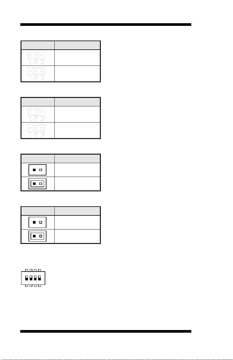
Setting the Jumpers
Jumpers are used on MI802 to select various settings and features
according to your needs and applications. Contact your supplier if you
have doubts about the be s t configu ration for your need s . The fo llowing
lists t he connectors on MI 802 and their respective functions.
Jumper Locations on MI802 ................................................................ 8
JP1: COM1 RS232 RI/+5V/+12V Power Setting ................................. 9
JP2: COM2 RS232 RI/+5V/+12V Power Setting ................................. 9
JP3: LCD Panel Power Selection ......................................................... 9
JP4: LCD Backlight Power Selection ................................................... 9
JP5: LCD BackLight Control Selection .............................................. 10
JP7: Clear CMOS Setting .................................................................. 10
JP8: LCD BackLight Co ntr ol Output Level........................................ 10
JP9: LCD Boot ROM Pro tect (factor y use only) ................................ 10
SW1: Panel Type Selection ................................................................ 10
MI802 User’s Manual 7
Page 12
INSTALLATIONS
Jumper Locations on MI802
Jumper Locations on MI802 ........................................................... Page
JP1: COM1 RS232 RI/+5V/+12V Power Setting ................................. 9
JP2: COM2 RS2 32 RI/ +5V/+12V Po wer Setting ................................. 9
JP3: LCD Panel Power Selection ......................................................... 9
JP4: LCD Backlight Power S election ................................................... 9
JP5: LCD BackLight Control Selection .............................................. 10
JP7: Clear CMOS Setting .................................................................. 10
JP8: LCD BackLight Co ntr ol Output Level ....................................... 10
JP9: LCD Boot ROM Pro tect (factor y use only) ................................ 10
SW1: Panel Type Selection ................................................................ 10
8
MI802 User’s Manual
Page 13
INSTALLATIONS
Pin 1-2
Short/Closed
Pin 3-4
Short/Closed
Pin 5-6
Short/Closed
Pin 1-2
Short/Closed
Pin 3-4
Short/Closed
Pin 5-6
Short/Closed
JP3
LCD Panel Power
1
3
2
4
5
6
Pin 1-2
Short/Closed
Pin 3-4
Short/Closed
Pin 5-6
Short/Closed
JP1: COM1 RS232 RI/+5V/+12V Power Setting
JP1 Setting Function
+12V
+5V
RI*
JP2: COM2 RS232 RI/+5V/+12V Power Setting
JP2 Setting Function
+12V
RI*
+5V
JP3: LCD Panel Power Selection
+3.3V*
+5V
JP4: LCD Backlight Power Selection
JP4 Setting Backlight Voltage
+3.3V
+5V
+12V*
MI802 User’s Manual 9
Page 14
INSTALLATIONS
JP5
Setting
JP7
Setting
JP8
Setting
21
21
JP9
Setting
21
21
1ON32
4
321 4
78 56
JP5: LCD BackLight Control Selection
Super I/O*
Reserved
JP7: Clear CMOS Setting
Normal*
Clear CMOS
JP8: LCD BackLight Control Output Level
+3.3V*
+5V
JP9: LCD Boot ROM Protect (factory use only)
*Default
SW1: Panel Type Selection
Default: Pin 1,2,3,4 OFF(1111)
10
Write
Normal*
MI802 User’s Manual
Page 15

INSTALLATIONS
SW1-4
SW1-3
SW1-2
SW1-1
Panel Type
ON ON ON ON 800*600 18bit 1ch
ON ON ON OFF 1024* 768 18bi t 1c h
ON ON OFF ON 1024*768 24bit 1ch
ON ON OFF OFF 1280* 768 18bit 1ch
ON OFF ON ON 1280*800 18bit 1ch
ON OFF ON OFF 1280*960 18bit 1ch
ON OFF OFF ON 1280*1024 24bit 2ch
ON OFF OFF OFF 1366* 768 18bi t 1c h
OFF ON ON ON 1366*768 24bit 1c h
OFF ON ON OFF 1440*900 24bit 2c h
OFF ON OFF ON 1440*1050 24bit 2ch
OFF ON OFF OFF 1600*900 24bit 2c h
OFF OFF ON ON 1680*1050 24bit 2c h
OFF OFF ON OFF 1600*1200 24bit 2ch
OFF OFF OFF ON 1920*1080 24bit 2c h
OFF OFF OFF OFF 1920*1200 24bit 2c h
MI802 User’s Manual 11
Page 16

INSTALLATIONS
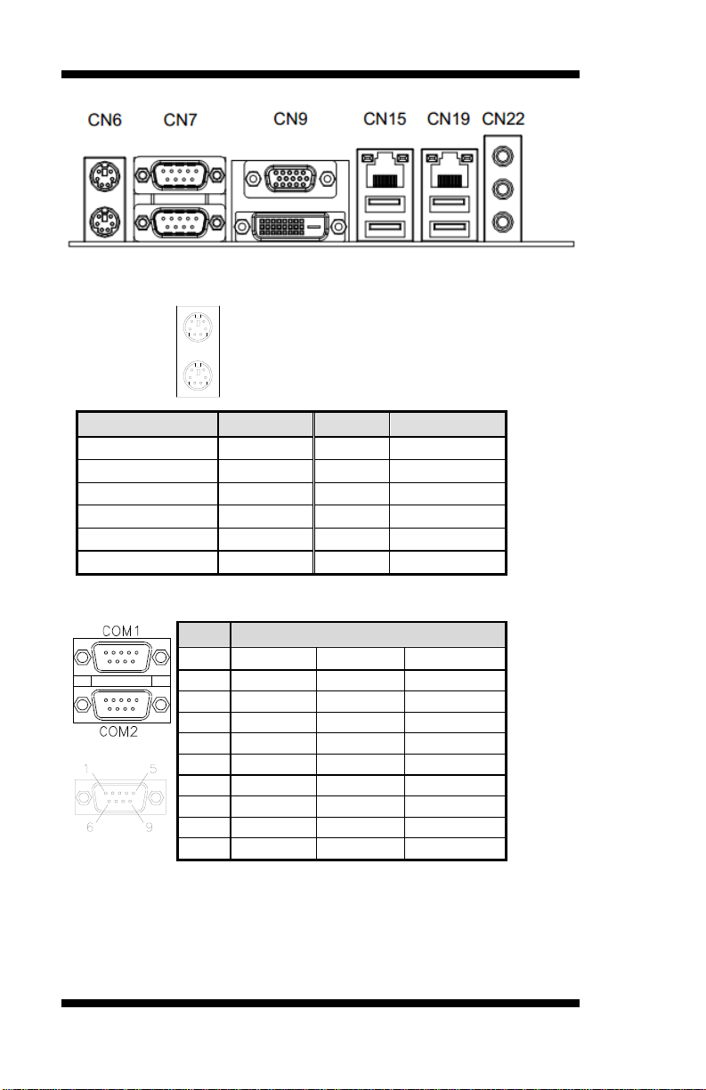
Connectors on MI802
The connectors on MI802 allows you to connect external devices such as
keyboard, fl oppy dis k driv es, hard di sk dri ves, pri nters, etc. The followi ng
table lists the connectors on MI802 and their respective fu nct ions.
Connect or Locations on MI802 ......................................................... 13
CN6: PS/2 Keyboard and PS/2 Mouse Connector s ............................ 14
CN7: COM1/RS232/422/485, COM2/RS232 Serial Po r t ................... 14
CN9: VGA and DVI-D Connecto r ..................................................... 15
CN15: GbE 1st RJ-45 and USB0/1 Ports ........................................... 15
CN19: GbE 2nd RJ-45 and USB2/3 Ports .......................................... 15
CN22: Line-in, Line-out & Microphone Connector ............................ 15
CN1, CN2, CN3, CN4: COM3/4/5/6 RS232 Serial Port .................... 16
CN5: ATX 4P +12V~24V Connector ................................................ 16
CN8, CN11: HDD Power Connecto r ................................................. 16
CN10, CN12: LVDS Connec tors (1st channel, 2nd channel) .............. 16
CN13: LCD Backlight Connector ...................................................... 17
CN14, CN1 6: SAT A C onnector s ....................................................... 17
CN17: USB6/7 Ports Header ............................................................. 17
CN18: iSMART JTAG Pin Header (factory use only) ........................ 17
CN20, CN21: Mini PCIE Connector .................................................. 17
CN23: Audio Connector (DF11 Connector)....................................... 18
CN24: Speaker Connector (JST Connector ) ...................................... 18
CPU_FAN1: CPU Fan Power Connector ........................................... 18
DIMM1, DI MM2 : D D R3 S O -DIMM ................................................ 18
J1: LPC Debug Connector (factory use only) ..................................... 18
J2 : Digital I/ O .................................................................................... 18
J3: System Function Connector .......................................................... 19
J5: USB4 Port ................................................................................... 19
J6: SPI Flash Connector (factory use only)......................................... 19
PCI1: PCI Slot (supports 2 Master) ................................................... 19
SYS_FAN1: System Fan Power Connector ....................................... 19
12
MI802 User’s Manual
Page 17
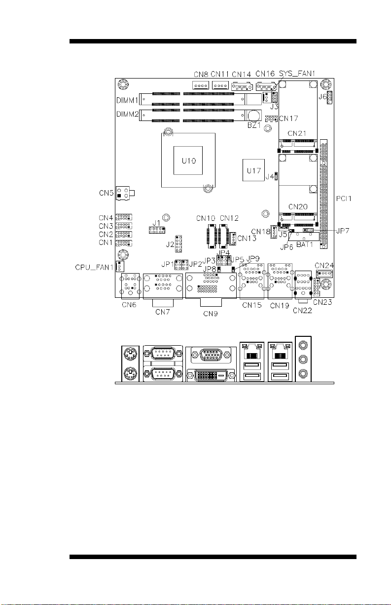
Connector Locations on MI802
INSTALLATIONS
MI802 User’s Manual 13
Page 18
INSTALLATIONS
Signal Name
Keyboard
Mouse
Signal Name
Keyboard dat a
1
7
Mouse data
N.C.
2 8 N.C.
GND
3 9 GND
+5V
4
10
+5V
Keyboard clock
5
11
Mouse clock
N.C.
6
12
N.C.
Pin #
Signal Name
RS-232
R2-422
RS-485
1
DCD
TX-
DATA-
2
RX
TX+
DATA+
3
TX
RX+
NC
4
DTR
RX-
NC
5
Ground
Ground
Ground
6
DSR
NC
NC
7
RTS
NC
NC
8
CTS
NC
NC
9*
RI
NC
NC
CN6: PS/2 Keyboard and PS/2 Mouse Connectors
PS/2 Mouse
PS/2 Keyboard
CN7: COM1/RS232/422/485, COM2/RS232 Serial Port
[
* Pin 9 supports RI/+5V/+12V function.
14
MI802 User’s Manual
Page 19
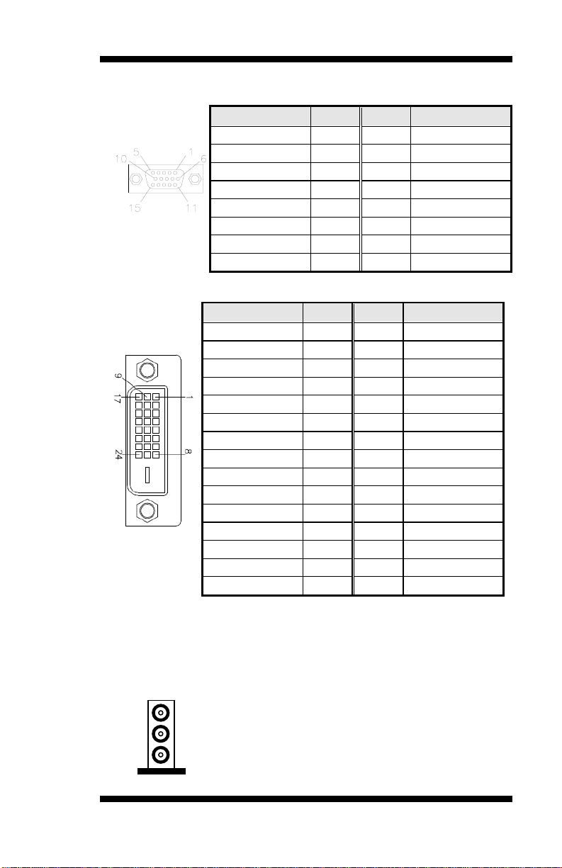
Signal Name
Pin #
Pin #
Signal Name
Red
1 2 Green
Blue
3 4 N.C.
GND
5 6 GND
GND
7 8 GND
+5V
9
10
GND
N.C.
11
12
DDC DATA
HSYNC
13
14
VSYNC
DDC CLOCK
15
Signal Name
Pin #
Pin #
Signal Name
DATA 2 -
1
16
HOT PLUG
DATA 2 +
2
17
DATA 0 -
Shield 2
3
18
DATA 0 +
N.C.
4
19
SHIELD 0
N.C.
5
20
N.C.
DDC CLOCK
6
21
N.C.
DDC DATA
7
22
SHIELD CLK
N.C
8
23
CLOCK-
DATA 1 -
9
24
CLOCK+
DATA 1 +
10
C1
N.C.
SHIELD 1
11
C2
N.C.
N.C.
12
C3
N.C.
N.C.
13
C4
N.C.
+5V
14
C5
N.C.
GROUND
15
C6
N.C.
L-IN
L-OUT
MIC
CN9: VGA and DVI-D Connector
VGA
[[[[
INSTALLATIONS
DVI-D
CN15: GbE 1st RJ-45 and USB0/1 Ports
CN19: GbE 2nd RJ-45 and USB2/3 Ports
CN22: Line-in, Line-out & Microphone Connector
MI802 User’s Manual 15
Page 20

INSTALLATIONS
2
1
10
9
Signal Name
Pin #
Pin #
Signal Name
DCD, Data carrier det ect
1 2 RXD, Receive data
TXD, Transmit data
3 4 DTR, Data termi n al ready
GND, ground
5 6 DSR, Data set r eady
RTS, Request to send
7 8 CTS, Clear to send
RI , Rin g indicator
9
10
Not Used
Signal Name
Pin #
Pin #
Signal Name
GND
1 2 GND
+12~24V
3 4 +12~24V
1
4
Pin #
Signal Name
1
+5V
2
Ground
3
Ground
4
+12V
2 1
1920
Signal Name
Pin #
Pin #
Signal Name
TX0-
2 1 TX0+
Ground
4 3 Ground
TX1-
6 5 TX1+
+5V/3.3V
8 7 Ground
TX3-
10 9 TX3+
TX2-
12
11
TX2+
Ground
14
13
Ground
TXC-
16
15
TXC+
+5V/3.3V
18
17
ENABKL
NC
20
19
NC
CN1, CN2, CN3, CN4: COM3/4/5/6 RS232 Serial Port
2X5_2.0mm_Straight_Male_DF11 (Haoguo DF11-10S-PA66H, Mating
connector: Hirose DF11-10DS-2C or compatible)
CN5: ATX 4P +12V~24V Connector
[[[[
CN8, CN11: HDD Power Connector
1X4_2.5mm_Straight_Male_Wafer (Haoguo W7-03H104142S1WT)
CN10, CN12: LVDS Connectors (1st channel, 2nd channel)
DF13-20
16
MI802 User’s Manual
Page 21

4 1
Pin #
Signal Name
1
+3.3V/5V/12V*
2
Backlight Enable
3
Brightness Control
4
Ground
17 4
Pin #
Signal Name
1
Ground
2
TX+
3
TX-
4
Ground
5
RX-
6
RX+
7
Ground
1
7
28
Signal Name
Pin #
Pin #
Signal Name
+5V
1 2 Ground
Data-
3 4 Data+
Data+
5 6 Data-
Ground
7 8 +5V
LVDS C onnectors : 2X10_1.25mm_Straight_Male_DF13 (Hirose
DF13-20DP-1.25V)
The LVDS (24bit) connectors on board consist of the first channel
(LVDS1) and second channel (LVDS2).
INSTALLATIONS
CN13: LCD Backlight Connector
1X4_2.0mm_Straight_M(JST B4B-PH-K-S)
CN14,CN16: SATA Conne ctors
CN17: USB6/7 Ports Header
2X4_2.0mm_Straight_Male_DF11 (Haoguo DF11-8S-PA66H, Mating
connector: Hirose DF11-8DS-2C or compatible)
CN18: iSMART JTAG Pin Header (factory use only)
CN20, CN21: Mini PCIE Connector
Remarks: CN20 USB signal is shared with J5.
MI802 User’s Manual 17
Page 22

INSTALLATIONS
1
12 11
2
Signal Name
Pin #
Pin #
Signal Name
LINEOUT_R
2 1 LINEOUT_L
Ground
4 3 JD LINEOUT
LINEIN R
6 5 LINEIN L
Ground
8 7 JD_LINEIN
MIC_R
10 9 MIC_L
Ground
12
11
JD MIC1
14
Pin #
Signal Name
1
Speaker-L+
2
Speaker-L-
3
Speaker-R-
4 Speaker-R+
3 1
Pin #
Signal Name
1
Ground
2
+12V
3
Rotat ion det ection
2
8
6
4
5
3
1
7
10
9
Signal Name
Pin #
Pin #
Signal Name
GND
1 2 +5V
OUT3
3 4 OUT1
OUT2
5 6 OUT0
IN3
7 8 IN1
IN2
9
10
IN0
CN23: Audio Connector (DF11 Connector)
2X6_2.0mm_Straight_Male_DF11 (Haoguo DF11-12S-PA66H, Mating
connector: Hirose DF11-12DS-2C or compatible)
CN24: Speaker Connector (JST Connector)
1X4_2.5mm_Straight_Male_Wafer (E-CALL 0110-071-040, Mating
connector: JST XHP-4 or compatible)
CPU_FAN1: CPU Fan Power Connector
DIMM1, DIMM2: DDR3 SO-DIMM
J1: LPC Debug Connector (factory use only)
J2: Digital I/O
2X5_2.54mm_Straight_Male_Pin Header ( E-CALL 0126-01-203-100)
18
MI802 User’s Manual
Page 23

INSTALLATIONS
2
8
6
4
1
7
5
3
Signal Name
Pin #
Pin #
Signal Name
Power BT N
1 2 Power BT N
Power LED+
3 4 Power LED-
HDD LED+
5 6 HDD LED-
Reset BTN
7 8 Reset BTN
1
5
Pin #
Signal Name
1
Ground
2
+5V
3
Ground
4
Data+
5
Data-
3 1
Pin #
Signal Name
1
Ground
2
+12V
3
Rotat ion det ection
J3: System Function Connector
2X4_2.0mm_Straight_Male_Pin Header (E-CALL 0196-01-200-080)
J5: USB4 Port
Remarks: Signal is shared w ith M ini PCIe(CN20)
1X5_1.25mm_Straight_Male_Wafer (E-CALL 0110-26110050, Mating
connector: Molex 51021-0500 or compatible)
J6: SPI Flash Connector (factory use only)
PCI1: PCI Slot (supports 2 Master)
SYS_FAN1: System Fan Power Connector
MI802 User’s Manual 19
Page 24

INSTALLATIONS
This page is intentionally left blank.
20
MI802 User’s Manual
Page 25

BIOS SETUP
BIOS Setup
This chapter describes the different sett ings available in the AMI BIOS
that comes with the board. The topics covered in this chapter are as
follows:
BIOS Introduction ............................................................................. 22
BIOS Setup ....................................................................................... 22
Advanced Settings ............................................................................. 24
Chipset Settings ................................................................................. 33
Boot Settings ..................................................................................... 38
Security Settings ................................................................................ 39
Save & Exit Settings .......................................................................... 40
MI802 User’s Manual 21
Page 26

BIOS SETUP
BIOS Introduction
The BIOS (Basic Input/Output System) installed in your computer
system’s ROM supports Intel processors. The BIOS provides critical
low-level support for a standard device such as disk drives, serial ports
and parallel po rt s. It also password p ro t ection as well as special suppo r t
for detailed fine-t uning of the chipset cont rolling the entire system.
BIOS Setup
The BIOS provides a Setup utility program for specifying the system
configurations and settings. The BIOS ROM of the system stores the
Se t u p u t ility. Whe n yo u t u r n on t h e c o mp u t e r, t he B I O S is imme dia t e ly
activated. Pressing the <Del> key immediately allows you to ent er the
Setup utility. If you are a little bit late pressing the <Del> key, POST
(Power On Self Tes t) will continue with its test rou tines, thus preventing
you f r om invokin g the S e tup. If yo u s till wis h to e n ter S etup, restart the
system by pressing the ”Reset” button or simultaneously pressing the
<Ctrl>, <Alt> and <Delete> keys. You can also restart by turning the
system Off and b ack On again. The following mes sage wi ll appear on the
screen:
Press <DEL> to Enter Setup
In general, you press the arrow keys to highli gh t items, <Enter> to select,
the <PgUp> and <PgDn> keys to change entries, <F1> for help and
<Esc> to quit.
When you enter the Setu p u tility, the Main Menu screen will appear on
the screen. The Main Menu allows you to select from various setup
functions and exit choices.
22
MI802 User’s Manual
Page 27

BIOS SETUP
Warning:
It is strongly recommended that you avoid making any
urer
↑↓
F3: Optimized Default
ESC: Exit
System Date
Sat 07/21/2012
System Time
13:03:22
changes to the chipset defaults. These defaults have been
carefully chosen by both AMI and your system manufact
to provide the absolute maximum performance and
reliability. Changing the defaults could cause the system to
become unstable and crash in some cases.
Main Advanced Chipset Boot Security Save & Exit
BIOS Information
→ ← Select Screen
Select Item
Enter: Select
+- Change Opt
F1: General Help
F2: Previous Values
F4: Save & EXIT
System Date
Set the Dat e. U se Tab t o switch between Data elements.
System Time
Set the Time. Use Tab to switch between Data elements.
MI802 User’s Manual 23
Page 28

BIOS SETUP
Legacy O pROM Support
↑↓
F3: Optimized Default
ESC: Exit
Launch PXE OpROM
Disabled
► PCI Subsystem Settings
►Auto Power On Schedule
► IDE Configur ation
Advanced Settings
This section allows you to configure and improve your system and allows
you to set u p some system features accor ding to your pr eference.
Main Advanced Chipset Boot Security Save & Exit
Lannch Sto r age OpROM Disabled
► ACPI Settings
► Wake up event setting
► CPU Configuration
► USB Configurat ion
► F81866 Super IO Configura tion
► FB81866 H/W Monitor
► PPM Configuration
Launch PXE OpROM
Enable or Disable Boot Opt ion for Legacy Networ k D evices.
Aptio Setup Utility
→ ← Select Screen
Select Item
Enter: Select
+- Change Opt
F1: General Help
F2: Previous Values
F4: Save & EXIT
24
MI802 User’s Manual
Page 29

Main Advanced Chipset Boot Security Save & Exit
↑↓
ESC: Exit
PCI ROM Priority
Legacy RO M
PCI Com m on Settings
VGA Palette Snoop
Disabled
PERR# Gene r ation
Disabled
SERR# Gene r ation
Disabled
PCI Subsystem Settings
BIOS SETUP
Aptio Setup Utility
PCI Bus Driver Version V 2.05.01
PCI Latency Timer 32 PCI Bus Clocks
→ ← Select Screen
Select Item
Enter: Select
+- Change Opt
F1: General Help
F2: Previous Values
F3: Optimized Default
F4: Save & EXIT
PCI ROM Priority
In case of multiple Option ROMs (Legacy and EFI Compatib le), specifies what
PCI Option ROM to launch.
PCI Latency Timer
Value to be programmed into PCI Latency Timer Register.
VGA Palette Snoop
Enables or Disables VGA Palette Registers Snooping.
PERR# Generation
Enables or Disables PCI Device to Generate PERR#.
SERR# Generation
Enables or Disables PCI Device to Generate SERR#.
MI802 User’s Manual 25
Page 30

BIOS SETUP
Main Advanced Chipset Boot Security Save & Exit
Enable ACPI Auto Conf igur ation Disabled
↑↓
ESC: Exit
Enable Hibe r nation
Enabled
ACPI Settings
Aptio Setup Utility
ACPI S ettings
→ ← Select Screen
Select Item
Enter: Select
+- Change Opt
F1: General Help
F2: Previous Values
F3: Optimized Default
F4: Save & EXIT
Enabled ACPI Auto Configuration
Enables or Disables BIOS ACPI Auto Configuration.
Enable Hibernation
Enabl e s o r D i sabl e s System abili ty to H i be rn a te (OS /S4 Sl e e p State). This option
may be not effective with some OS.
26
MI802 User’s Manual
Page 31

Main Advanced Chipset Boot Security Save & Exit
↑↓
ESC: Exit
Wake on Ring
Disabled
Wake on PCIE PME
Disabled
Wake Up Event Setting
Aptio Setup Utility
Wake on Ring
The optio ns are Disabled and Enabled.
Wake on PCIE PME
The options are Disabled and Enabled.
BIOS SETUP
→ ← Select Screen
Select Item
Enter: Select
+- Change Opt
F1: General Help
F2: Previous Values
F3: Optimized Default
F4: Save & EXIT
MI802 User’s Manual 27
Page 32

BIOS SETUP
Main Advanced Chipset Boot Security Save & Exit
CPU Configura tion
↑↓
ESC: Exit
Processor Type
Intel(R) Atom(TM) CPU
EMT64
Not Suppor ted
Processor Speed
1865 MHz
System Bus Speed
533 MHz
14 Actua l Ratio
14
System Bus Speed
533 MHz
Processor Stepping
30661
Microcode Revision
265
L1 Cache RAM
2x56 k
L2 Cache RAM
2x512 k
Processor Core
Dual
Hyper-Threading
Supported
Hyper-Threading
Enabled
Enabled Limit CPUID Maximum
Disabled
CPU Configuration
This section shows t he CPU configu r ation parameters.
Aptio Setup Utility
Ratio Status
→ ← Select Screen
Select Item
Enter: Select
+- Change Opt
F1: General Help
F2: Previous Values
Execute Disable Bit
F3: Optimized Default
F4: Save & EXIT
Hyper-threading
Enabl e d for Windows XP and Linux (OS optimized for Hyper-Threading
Technology) and Disabled for ot her OS (OS not optimized for
Hyper-Threa ding Technology). When Disabled, only one thread per
enabled core is enabled.
Execute Disable Bit
XD can prevent certain classes of m al i ci ous buf f er overfl ow attacks when
combined with a supporting OS (Windows Server 2003 SP1, Windows
XP SP2, SuSE Linux 9.2, Re33dHat Enterprise 3 Update 3.)
Limit CPUID Maximum
Disabled fo r Windows XP.
28
MI802 User’s Manual
Page 33

Main Advanced Chipset Boot Security Save & Exit
Auto P ower O n S c hedule
↑↓
ESC: Exit
Disable
Schedule Slot 1
None
Schedule Slot 2
None
Advanced
↑↓
ESC: Exit
SATA Port0
Not Present
SATA Port1
Not Present
SATA Controller(s)
Enabled
Configure S ATA a s
IDE
BIOS SETUP
iSmart Co ntroller
Aptio Setup Utility
Power-On after Power failure
→ ← Select Screen
Select Item
Enter: Select
+- Change Opt
F1: General Help
F2: Previous Values
F3: Optimized Default
F4: Save & EXIT
EuP/ErP Standby Power Control
Saving the po w er co ns umption on power o ff.
Power-On after Power Failure
This field sets the system power status whether on or off when power returns to
the system from a power failure situation.
Schedule Slot
None / Power On / Power On/Off – Setup the hour/minute for system power on
IDE Configuration
Main
Chipset Boot Security Save & Exit
Aptio Setup Utility
→ ← Select Screen
Select Item
Enter: Select
+- Change Opt
F1: General Help
F2: Previous Values
F3: Optimized Default
F4: Save & EXIT
SATA Controller(s)
Enable / Dis able Serial ATA Controller.
Configure SATA as
(1) IDE Mode.
(2) AHCI Mode.
MI802 User’s Manual 29
Page 34

BIOS SETUP
Main Advanced Chipset Boot Security Save & Exit
↑↓
USB Devices:
None
Enabled EHCI Hand-off
Enabled
USB hardware delays and time-outs:
USB Transfer time-out
20 sec
20 sec Device power-up delay
Auto
USB Configuration
Aptio Setup Utility
USB Configuration
→ ← Select Screen
Select Item
Enter: Select
Legacy USB Support
Device reset time-out
+- Change Opt
F1: General Help
F2: Previous Values
F3: Optimized Default
F4: Save & EXIT
ESC: Exit
Legacy USB Support
Enables Legacy USB supp ort.
AUTO option disables legacy support if no USB devices are connected.
DISABLE option will keep USB devices availab le only for EF I
applications.
EHCI Hand-off
Enabled/Disabled. This is a workaround for OSes without EHCI hand-off
support. The EHCI ownership change sh ould be cl ai m ed by EHCI driver.
USB Tra nsfer Time-out
The time-out value for Control, Bulk, and Interrupt t r ansfers.
Device Reset Time-out
USB mass Storage device start Unit command time-out.
Device Power-up Delay
Maximu m time the device will take before it properly reports itself to the
Host C ontr ol l e r. ‘Auto’ uses def aul t value: for a Root port it is 100ms, f or
a Hub port the delay is taken from Hub descriptor.
30
MI802 User’s Manual
Page 35

Main Advanced Chipset Boot Security Save & Exit
↑↓
F81866 Super IO Chip
F81866
►Serial Port 0 Configur ation
►Serial Port 1 Configur ation
►Serial Port 3 Configur ation
►Serial Port 4 Configur ation
Power Failure I
Always off
KB/MS Power on
None
All Enable
Super IO Configuration
Aptio Setup Utility
F81866 Super IO Configuration
►Serial Port 2 Configur ation
►Serial Port 5 Configurat ion
BIOS SETUP
→ ← Select Screen
Select Item
Enter: Select
+- Change Opt
F1: General Help
F2: Previous Values
F3: Optimized Default
F4: Save & EXIT
ESC: Exit
F81866 ERP Support
Serial Port Configuration
Set Parameters o f Serial Ports. User can Enable/Disable the serial port
and Select an optimal settings for the Super IO Device.
MI802 User’s Manual 31
Page 36

BIOS SETUP
Main Advanced Chipset Boot Security Save & Exit
↑↓
CPU temperature
+52 C
System temperat ure
+54 C
Fan1 Speed
N/A
N/A Vcore
+1.208
VCC5V
+5.129V
VCC12V
+11.528 V
+1.5V
+1.520 V
+5.040 V VCC3V
+3.392 V
VSB3V
+3.376 V
CPU FAN1
Disabled
SYS FAN1
Disabled
Main Advanced Chipset Boot Security Save & Exit
PPM Configuration
↑↓
ESC: Exit
EIST
Enabled
H/W Monitor
Aptio Setup Utility
PC Health S tatus
Fan2 Speed
→ ← Select Screen
Select Item
Enter: Select
VSB5V
+- Change Opt
F1: General Help
F2: Previous Values
F3: Optimized Default
F4: Save & EXIT
ESC: Exit
Temperatures/Voltages
These fields are the parameters of the hardware monitoring function
feature of the motherboard. The values are read-only values as monitored
by the system and sho w the P C health statu s .
CPU Fan1 Control
Options are: Disabled (default), 50 ℃, 60 ℃, 70 ℃, 80 ℃
SYS Fan2 Control
Options are: Disabled (default), 50 ℃, 60 ℃, 70 ℃, 80 ℃
PPM Configuration
Aptio Setup Utility
32
MI802 User’s Manual
→ ← Select Screen
Select Item
Enter: Select
+- Change Opt
F1: General Help
F2: Previous Values
F3: Optimized Default
F4: Save & EXIT
Page 37

BIOS SETUP
Chipset
↑↓
ESC: Exit
► South Bridge
Main Advanced Chipset Boot Security Save & Exit
↑↓
► Intel IGD Configur ation
************Memory Information************
Memory Frequency
1067 MHz(DDR3)
Total Memory
2048 MB
DIMM#0
Not Present
DIMM#1
2048 MB
Chipset Settings
This section allows you to configure and improve your system and allows
you to set u p some system features accor ding to your pr eference.
Main Advanced
Aptio Setup Utility
Boot Security Save & Exit
► Host Bridge
→ ← Select Screen
Select Item
Enter: Select
+- Change Field
F1: General Help
F2: Previous Values
F3: Optimized Default
F4: Save
Host Bridge
This item shows the Host Bridge Parameters.
South Bridge
This item shows the South Bridge Parameters.
Host Bridge
This section allows you to co nfigure the Host Bridge Chipset.
► Memory Frequency and Timing
Aptio Setup Utility
→ ← Select Screen
Select Item
Enter: Select
+- Change Opt
F1: General Help
F2: Previous Values
F3: Optimized Default
F4: Save & EXIT
ESC: Exit
MI802 User’s Manual 33
Page 38

BIOS SETUP
Main Advanced Chipset Boot Security Save & Exit
↑↓
ESC: Exit
MRC Fast Boot
Enabled
Dynamic
Main Advanced Chipset Boot Security Save & Exit
↑↓
ESC: Exit
IGFX-Boot Type
VBI OS Default
Memory Frequency and Timing
Aptio Setup Utility
Memory Frequency and Timing
Max TOLUD
MRC Fast Boot
The options are Disabled and Enabled.
Max TOLUD
The defa ult settin g is D ynamic.
Intel IGD Configuration
Aptio Setup Utility
Inte l IGD Configuration
→ ← Select Screen
Select Item
Enter: Select
+- Change Opt
F1: General Help
F2: Previous Values
F3: Optimized Default
F4: Save & EXIT
→ ← Select Screen
Select Item
Enter: Select
+- Change Opt
F1: General Help
F2: Previous Values
F3: Optimized Default
F4: Save & EXIT
IGFX-Boot Type
Select the video Device which will be activated during POST.
34
MI802 User’s Manual
Page 39

BIOS SETUP
Chipset
↑↓
ESC: Exit
►
TPT Device
►
PCI Express Roo t Port0
► PCI Express Roo t Port1
► PCI Express Roo t Port3
DMI Link ASPM Control
Enabled
PCI-Exp. High Priority Port
Disabled
High Precisio n E v ent Timer Configuration
High Precisio n Timer
Enabled
1
South Bridge
This section allows you to configure the South Bridge Chipset .
Main Advanced
Aptio Setup Utility
Boot Security Save & Exit
► PCI Express Roo t Port2
→ ← Select Screen
Select Item
SLP_SP4 Assertion Width
-2 Seconds
Enter: Select
+- Change Opt
F1: General Help
F2: Previous Values
F3: Optimized Default
F4: Save & EXIT
DMI Clink ASPM Control
The control of Active State Power Managemen t on both NB side and SB
sid e of the DMI Link.
PCI-Exp. High Priority Port
The options are Disabled, Port1, Port2, Port3, and Port4.
High Precision Event Timer Configuration
Enable/or Disable the High Precision Event Timer.
SLP_S4 Assertion Stretch Enable
Select a minimum assertion width of the SLP_S4# signal.
MI802 User’s Manual 35
Page 40

BIOS SETUP
Main Advanced Chipset Boot Security Save & Exit
↑↓
Azalia Contro ller
HD Audio Select USB Mode
By Controllers
UHCI #1 (por t 0 and 1)
Enabled
Enabled UHCI #3 (por t 4 and 5)
Enabled
UHCI #4 (por t 6 and 7)
Enabled
USB 2.0(EHCI ) S upport
Enabled
Main Advanced Chipset Boot Security Save & Exit
↑↓
ESC: Exit
Enabled Port 0 IOx APIC
Disabled
Automatic A SPM
Manual
ASPM L0s
Root Port Only
ASPM L1
Enabled
Chipset
↑↓
ESC: Exit
PCI Express Port 1
Auto
Port 0 IOx APIC
Disabled
Auto
TPT Device
Aptio Setup Utility
UHCI #2 (por t 2 and 3)
PCI Express Root Port0
Aptio Setup Utility
→ ← Select Screen
Select Item
Enter: Select
+- Change Opt
F1: General Help
F2: Previous Values
F3: Optimized Default
F4: Save & EXIT
ESC: Exit
PCI Express Port 0
PCI Express Root Port1
Main Advanced
Automatic A SPM
Boot Security Save & Exit
→ ← Select Screen
Select Item
Enter: Select
+- Change Opt
F1: General Help
F2: Previous Values
F3: Optimized Default
F4: Save & EXIT
Aptio Setup Utility
→ ← Select Screen
Select Item
Enter: Select
+- Change Opt
F1: General Help
F2: Previous Values
F3: Optimized Default
F4: Save & EXIT
36
MI802 User’s Manual
Page 41

Main Advanced Chipset Boot Security Save & Exit
↑↓
ESC: Exit
PCI Express Port 2
Auto
Port 0 IOx APIC
Disabled
Automatic A SPM
Auto
Main Advanced Chipset Boot Security Save & Exit
↑↓
ESC: Exit
PCI Express Port 3
Enabled
Disabled Automatic A SPM
Auto
PCI Express Root Port2
Aptio Setup Utility
PCI Express Root Port3
Aptio Setup Utility
Port 0 IOx APIC
BIOS SETUP
→ ← Select Screen
Select Item
Enter: Select
+- Change Opt
F1: General Help
F2: Previous Values
F3: Optimized Default
F4: Save & EXIT
→ ← Select Screen
Select Item
Enter: Select
+- Change Opt
F1: General Help
F2: Previous Values
F3: Optimized Default
F4: Save & EXIT
MI802 User’s Manual 37
Page 42

BIOS SETUP
Main Advanced Chipset Boot Security Save & Exit
↑↓
Setup Prompt Timeout
1
Bootup NumLock State
On
Quiet Boot
Disabled
CSM16 Module Version
07.68
Option ROM Me ssages
Force BIO S
Inte r r upt 19 Canture
Enabled
CSM Support
Enabled
Boot Settings
Aptio Setup Utility
Boot Configuration
Fast Boot
Disabled
→ ← Select Screen
Select Item
GateA20 Active Upon Reques t
Boot Option Prio r ities
Enter: Select
+- Change Opt
F1: General Help
F2: Previous Values
F3: Optimized Default
F4: Save & EXIT
ESC: Exit
Setup Prompt Timeout
Number of seconds to wait for setup activation key.
65535(0xFFFF) means indefinite waiting.
Bootup NumLock State
Select the keyboard NumLock state.
Quiet Boot
Enables/Disables Quiet Boot option.
Fast Boot
Enables/Disables boot with initialization of a minimal set of devices required
to launch active boot option. Has no effect for BBS boot options.
GateA20 Active
UPON REQUEST – GA20 can be disabled using BIOS services.
ALWAYS – do not allow disabling GA20; this option is useful when any RT
code is executed above 1MB.
Option ROM Messages
Set display mode for Option ROM. Options: Force BIOS and Keep Current.
Interrupt 19 Capture
Enable: Allows Option ROMs to trap Int 19.
CSM Support
Enables/Disables/Auto CSM Support.
38
MI802 User’s Manual
Page 43

BIOS SETUP
Main Advanced Chipset Boot Security Save & Exit
Password Description
↑↓
ESC: Exit
If ONLY the Administrator’s password is set, t he n
to Setup and is only asked
Administrator Password
Security Settings
This section allows you to configure and improve your system and allows
you to set up some system features according to your preference.
this only limits access
for when entering Setup.
If ONLY the User’s password is set, then this is a
power on password and must be entered to boot or
enter S etup. I n S etup the User will have
Administrator right s
User Password
Administra tor Password
Set Set up Administrator Password.
User Password
Set User Password.
Aptio Setup Utility
→ ← Select Screen
Select Item
Enter: Select
+- Change Opt
F1: General Help
F2: Previous Values
F3: Optimized Default
F4: Save & EXIT
MI802 User’s Manual 39
Page 44

Save & Exit
Save Changes and Exit
↑↓
Discard Changes and Ex it
Save Changes and Reset
Discard Changes and Res et
Save Options
Save Changes
Discard Changes
Restore Defaults
Restore User Defaults
Boot Override
BIOS SETUP
Save & Exit Settings
Main Advanced Chipset Boot Security
Aptio Setup Utility
→ ← Select Screen
Select Item
Enter: Select
+- Change Opt
F1: General Help
F2: Previous Values
Save as User Defaults
F3: Optimized Default
F4: Save & EXIT
ESC: Exit
Save Changes and Exit
Exit system setup after saving the changes.
Discard Changes and Exit
Exit system set up without s aving any changes.
Save Changes and Reset
Reset the system after saving the changes.
Discard Changes and Reset
Reset system setup without saving any changes.
Save Changes
Save Changes done so far to any of the setup options.
Discard Changes
Discard Changes done so far to any of the setup options.
Restore Defaults
Restore/Lo ad Defaults values for all the setup options.
Save as User Defaults
Save the changes done so far as User Defaults.
Restore User Defaults
Restore the User Defaults to all the setup options.
40
MI802 User’s Manual
Page 45

DRIVERS INSTALLATION
Drivers Installation
This section describes the installation procedures for software and
drivers. The software and drivers are included with the motherboard. I f
you fi nd the i tems m issing, please contact the vendor where you made the
purchase. The contents of this s ection include the followin g:
Intel Chipset Soft ware I nst allation Utility ........................................... 42
VG A Driver s Installation ................................................................... 43
Realtek HD Audio Dr iver Insta llation ................................................ 44
LAN Driver s Installation .................................................................... 45
IMPORTANT NOTE:
After installing your Windows operating system, you must install first the
Intel Chipset Softwar e I nstallation Utility before proceeding with the
drivers ins tallation.
MI802 User’s Manual 41
Page 46

DRIVERS INSTALLATION
Intel Chipset Software Installation U t ility
The I ntel Chipset D rivers should be installed first before the softwar e
drivers to enable Plug & Play INF support for I nt el chipset components.
Follow th e instructions be low to complete the installa tion.
1. Insert the disc that comes with the board. Click Intel and then Intel(R)
Cedarview Chipset Drivers.
2. Click Intel(R) Chipset Software Installation Utility.
3. When the Welcome screen to the Intel® Chipset Device S oftware
appears, click Next to c ontinue .
4. Click Yes to accept the software license agreement and proceed with
the installation process.
5. O n the Readme File Information screen, click Next to cont inue the
installation.
6. The Setup pr ocess is now complete. Click Finish to restart the
computer and for changes to take effect.
42
MI802 User’s Manual
Page 47

DRIVERS INSTALLATION
VGA Drivers I n sta lla tio n
1. Click Intel(R) Cedarview Graphic s Dri v er.
2. When the Welcome screen appears, click Next to continue .
4. Click Yes to t o agree with the license agreement and continue the
installation.
5. O n the Readme File Information screen, click Next to cont inue the
installation of the Intel® Graphics Media Accelerator Driver.
6. On Setup Progress screen, click Next to continue.
7. Setup complete. Click Finish to restart t he computer and for changes
to t ak e effect.
MI802 User’s Manual 43
Page 48

DRIVERS INSTALLATION
Realtek HD Audio Driver Installation
1. Click Realtek High Definition Audio Driver.
2. On the Welcome to the InstallShield Wizard screen, click Next to
proceed with and complete the installation process.
3. Restart the computer when prompted.
44
MI802 User’s Manual
Page 49

DRIVERS INSTALLATION
LAN D riv e r s In s ta llat ion
1. Insert the CD t hat comes with the board. Click LAN Card and then
Realtek LAN Controller Drivers.
2. Click Realtek RTL8111E LAN Drivers.
3. In the Welcome screen, click Next.
4. In the License Agreement screen, click I accept the terms in li cense
agreement and Next to accept the software license agreement and
proceed with the installation process.
5. Click the checkb ox for Drivers in the Setup Options screen to select it
and click Next to c ontinue.
6. When the Ready to Install the Program screen appears, click Install to
continue.
7. When InstallShield Wiz ard is complete, click Finish.
MI802 User’s Manual 45
Page 50

DRIVERS INSTALLATION
This pa ge is intent iona lly left blank .
46
MI802 User’s Manual
Page 51

Address
Device Description
000h - 01Fh
DMA Controller #1
020h - 03Fh
Interrupt Controller #1
040h - 05Fh
Timer
060h - 06Fh
Keyboard Cont r oller
070h - 07Fh
Real Time Clock, NMI
080h - 09Fh
DMA Page Register
0A0h - 0BFh
Interrupt Controller #2
0C0h - 0DFh
DMA Contro ller #2
0F0h
Clear Math Coprocessor Busy Signal
0F1h
Reset Math Coprocessor
1F0h - 1F7h
IDE Interface
2B0h - 2DFh
Graphics adapter Contro ller
2E8h - 2EFh
Se rial Port #4(COM4)
2F8h - 2FFh
Serial Port #2(COM2)
360h - 36Fh
Network Ports
3B0h - 3BFh
Monochrome & Printer adapter
3C0h - 3CFh
EGA adapter
3D0h - 3DFh
CGA adapter
3E8h - 3EFh
Se rial Port #3(COM3)
3F8h - 3FFh
Serial Port #1(COM1)
Appendix
A. I/O Port Address Map
Each peripheral device in the system is assigned a set of I/O port
addresses that al so becomes the iden tity of the devi ce. The foll owing table
lists the I/O po r t addresses use d.
APPENDIX
MI802 User’s Manual 47
Page 52

APPENDIX
Level
Function
IRQ0
Sys tem Timer Ou tp ut
IRQ1
Keyboard
IRQ2
Interrupt Cascade
IRQ3
Se rial Port #2
IRQ4
Se rial Port #1
IRQ5
Reserved
IRQ6
Reserved
IRQ7
Reserved
IRQ8
Real Time Clock
IRQ9
Reserved
IRQ10
Seria l Po rt #4
IRQ11
Se rial Port #3
IRQ12
PS/2 Mo u se
IRQ13
80287
IRQ14
Primary IDE
B. Interrupt Request Lines (IRQ)
Peripheral devi ces use i nterrupt request li nes to notify CPU for the service
required. The following table shows the IRQ used by the devices on
board.
48
MI802 User’s Manual
Page 53

APPENDIX
C. Watchdog Timer Configuration
The WDT is used to generate a variety of output signals after a user
programmable count. The WDT is suitable for use in the prevention of
system lock-up, such as when software becomes trapped in a deadlock.
Under these sorts of circumstances, the timer will count to zero and t he
selected outputs will be driven. Under normal cir cu mstance, t he user will
restart the WDT at regular intervals before the timer counts to zero.
SAMPLE CODE:
//--------------------------------------------------------------------------#include <dos.h>
#include <conio.h>
#include <stdio.h>
#include <stdlib.h>
#include "F81866.H"
//--------------------------------------------------------------------------int main (int argc, char *argv[]);
void EnableWDT (int);
void DisableWDT(void);
//--------------------------------------------------------------------------int main (int argc, char *argv[])
{
unsigned char bBuf;
unsigned char bTime;
char **endptr;
char SIO;
printf("Fintek 81865 watch dog program\n");
SIO = Init_F81866();
if (SIO == 0)
{
printf("Can not detect Fintek 81865, program abort.\n");
return(1);
}//if (SIO == 0)
if (argc != 2)
{
printf(" Parameter incorrect!!\n");
return (1);
}
bTime = strtol (argv[1], endptr, 10);
printf("System will reset after %d seconds\n", bTime);
if (bTime)
{ EnableWDT(bTime); }
else
{ DisableWDT(); }
return 0;
}
//--------------------------------------------------------------------------void EnableWDT (int interval)
{
unsigned char bBuf;
MI802 User’s Manual 49
Page 54

APPENDIX
bBuf = Get_F81866_Reg(0x2B);
bBuf &= (~0x20);
Set_F81866_Reg(0x2B, bBuf); //Enable WDTO
Set_F81866_LD(0x07); //switch to logic device 7
Set_F81866_Reg(0x30, 0x01); //enable timer
bBuf = Get_F81866_Reg(0xF5);
bBuf &= (~0x0F);
bBuf |= 0x52;
Set_F81866_Reg(0xF5, bBuf); //count mode is second
Set_F81866_Reg(0xF6, interval); //set timer
bBuf = Get_F81866_Reg(0xFA);
bBuf |= 0x01;
Set_F81866_Reg(0xFA, bBuf); //enable WDTO output
bBuf = Get_F81866_Reg(0xF5);
bBuf |= 0x20;
Set_F81866_Reg(0xF5, bBuf); //start co un ting
}
//--------------------------------------------------------------------------void DisableWDT(void)
{
unsigned char bBuf;
Set_F81866_LD(0x07); //switch to logic device 7
bBuf = Get_F81866_Reg(0xFA);
bBuf &= ~0x01;
Set_F81866_Reg(0xFA, bBuf); //disable WDTO output
bBuf = Get_F81866_Reg(0xF5);
bBuf &= ~0x20;
bBuf |= 0x40;
Set_F81866_Reg(0xF5, bBuf); //d isable WDT
}
//---------------------------------------------------------------------------
50
MI802 User’s Manual
Page 55

//--------------------------------------------------------------------------#include "F81866.H"
#include <dos.h>
//--------------------------------------------------------------------------unsigned int F81866_BASE;
void Unlock_F81866 (void);
void Lock_F81866 (void);
//--------------------------------------------------------------------------unsigned int Init_F81866(void)
{
unsigned int result;
unsigned char ucDid;
F81866_BASE = 0x4E;
result = F81866_BASE;
ucDid = Get_F81866_Reg(0x20);
if (ucDid == 0x07) //Fintek 81865
{ goto Init_Finish; }
F81866_BASE = 0x2E;
result = F81866_BASE;
ucDid = Get_F81866_Reg(0x20);
if (ucDid == 0x07) //Fintek 81865
{ goto Init_Finish; }
F81866_BASE = 0x00;
result = F81866_BASE;
Init_Finish:
return (result);
}
//--------------------------------------------------------------------------void Unlock_F81866 (void)
{
outportb(F81866_INDEX_PORT, F 81866_U NLOCK );
outportb(F81866_INDEX_PORT, F 81866_U NLOCK );
}
//--------------------------------------------------------------------------void Lock_F81866 (void)
{
outportb(F81866_INDEX_PORT, F 81866_LOCK );
}
//--------------------------------------------------------------------------void Set_F81866_LD( unsigned char LD)
{
Unlock_F81866();
outportb(F81866_INDEX_PORT, F 81866_REG_LD);
outportb(F81866_DATA_PORT, LD);
Lock_F81866();
}
//--------------------------------------------------------------------------void Set_F81866_Reg( unsigned char REG, unsigned char DATA)
{
Unlock_F81866();
outportb(F81866_INDEX_PORT, REG);
outportb(F81866_DATA_PORT, D ATA);
Lock_F81866();
}
//--------------------------------------------------------------------------unsigned char Get_F81866_Reg(unsigned char REG)
{
unsigned char Result;
Unlock_F81866();
outportb(F81866_INDEX_PORT, REG);
Result = inportb(F81866_DATA_PORT);
Lock_F81866();
return Result;
}
//---------------------------------------------------------------------------
APPENDIX
MI802 User’s Manual 51
Page 56

APPENDIX
//--------------------------------------------------------------------------#ifndef __F81866_H
#define __F81866_H 1
//--------------------------------------------------------------------------#define F81866_INDEX_PORT (F81866_BASE)
#define F81866_DATA_PORT (F81866_BASE+1)
//--------------------------------------------------------------------------#define F81866_REG_LD 0x07
//--------------------------------------------------------------------------#define F81866_UNLOCK 0x87
#define F81866_LOCK 0xAA
//--------------------------------------------------------------------------unsigned int Init_F81866(void);
void Set_F81866_LD( unsigned char);
void Set_F81866_Reg( unsigned char, unsigned char);
unsigned char Get_F81866_Reg( unsigned char);
//--------------------------------------------------------------------------#endif //__F81866_H
52
MI802 User’s Manual
Page 57

D. Digita l I/O S a mple C o d e
Files of the MAIN.CPP
//--------------------------------------------------------------------------#include <dos.h>
#include <conio.h>
#include <stdio.h>
#include <stdlib.h>
#include "F81866.H"
#define BIT0 0x01
#define BIT1 0x02
#define BIT2 0x04
#define BIT3 0x08
#define BIT4 0x10
#define BIT5 0x20
#define BIT6 0x40
#define BIT7 0x80
//--------------------------------------------------------------------------int main (void) ;
void Dio3Initial(void);
void Dio3SetOutput(unsigned char);
unsigned char Dio3GetInput(void);
void Dio3SetDirection(unsigned char);
unsigned char Dio3GetDirection(void);
//--------------------------------------------------------------------------int main (void)
{
char SIO;
unsigned char DIO;
printf("Fintek 81866 digital I/O test program. Ver 2.0\n");
SIO = Init_F81866();
if (SIO == 0)
{
printf("Can not detect Fintek 81866, program abort.\n");
return(1);
}//if ( S I O == 0)
Dio3Initial();
/*
//for GPIO30..37
Dio3SetDirection(0xF0); //GP30..33 = input, GP34..37=output
printf("Current DIO direction = 0x%X\n", Dio3GetDirection());
printf("Current DIO status = 0x%X\n", Dio3GetInput());
printf("Set DIO output to high\n");
Dio3SetOutput(0x0F);
printf("Set DIO output to low\n");
Dio3SetOutput(0x00);
*/
//for GPIO30..37
Dio3SetDirection(0xF0); //GP30..33 = input, GP34..37=output
Dio3SetOutput(0x00); //clear
// DIO = Dio3GetInput() & 0x0F;
APPENDIX
MI802 User’s Manual 53
Page 58

APPENDIX
Dio3SetOutput(0x00); //clear
DIO = Dio3GetInput() & 0x0F;
if (DIO != 0x0A)
{
printf("The Fintek 81866 digital IO abnormal, abort.\n");
return(1);
}//if ( DIO != 0x0 A)
Dio3SetOutput(0xA0); //clr# is high
Dio3SetOutput(0xF0); //clk and clr# is high
Dio3SetOutput(0xA0); //clr# is high
DIO = Dio3GetInput() & 0x0F;
if (DIO != 0x05)
{
printf("The Fintek 81866 digital IO abnormal, abort.\n");
return(1);
}
pr intf("!!! Pa ss !!!\n");
return 0;
}
//--------------------------------------------------------------------------void Dio3Initial(void)
{
unsigned char ucBuf;
// Switc h GPIO multi-function pin for gpio 30~37
// Multi Pin Select UART2/GPIOs
// bit[6:5] 0:UART2 / 1:GPIOs
ucBuf = Get_F81866_Reg(0x28);
ucBuf |= BIT5;
Set_F81866_Reg(0x28, ucBuf);
Set_F81866_LD(0x06); //sw itch to logic device 6
//enable the GP3 group
ucBuf = Get_F81866_Reg(0x30);
ucBuf |= 0x01;
Set_F81866_Reg(0x30, ucBuf);
Set_F81866_Reg(0x88, 0x00); //define as input mode
//Set_F81866_Reg(0xA3, 0xFF); //push pull mode
}
//--------------------------------------------------------------------------void Dio3SetOutput(unsigned char NewData)
{
Set_F81866_LD(0x06); //sw itch to logic device 6
Set_F81866_Reg(0x89, NewData);
}
//--------------------------------------------------------------------------unsigned char Dio3GetInput(void)
{
unsigned char result;
Set_F81866_LD(0x06); //sw itch to logic device 6
result = Get_F81866_Reg(0x8A);
return (result);
}
54
MI802 User’s Manual
Page 59

APPENDIX
//--------------------------------------------------------------------------void Dio3SetDirection(unsigned char NewData)
{
//NewData : 1 for input, 0 for output
Set_F81866_LD(0x06); //sw itch to logic device 6
Set_F81866_Reg(0x88, NewData);
}
//--------------------------------------------------------------------------unsigned char Dio3GetDirection(void)
{
unsigned char result;
Set_F81866_LD(0x06); //sw itch to logic device 6
result = Get_F81866_Reg(0x88);
return (result);
}
//---------------------------------------------------------------------------
MI802 User’s Manual 55
Page 60

APPENDIX
Files of the F81866.CPP
//--------------------------------------------------------------------------#include "F81866.H"
#include <dos.h>
//--------------------------------------------------------------------------unsigned int F81866_BASE;
void Unlock_F81866 (void);
void Lock_F81866 (void);
//--------------------------------------------------------------------------unsigned int Init_F81866(void)
{
unsigned int result;
unsigned char ucDid;
F81866_BASE = 0x4E;
result = F81866_BASE;
ucDid = Get_F81866_Reg(0x20);
if (ucDid == 0x10) //Fintek 81801
{ goto Init_Finish; }
F81866_BASE = 0x2E;
result = F81866_BASE;
ucDid = Get_F81866_Reg(0x20);
if (ucDid == 0x07) //Fintek 81801
{ goto Init_Finish; }
F81866_BASE = 0x00;
result = F81866_BASE;
Init_Finish:
return (result);
}
//--------------------------------------------------------------------------void Unlock_F81866 (void)
{
outportb(F81866_INDEX_PORT, F81866_UNLOCK);
outportb(F81866_INDEX_PORT, F81866_UNLOCK);
}
//--------------------------------------------------------------------------void Lock_F81866 (void)
{
outportb(F81866_INDEX_PORT, F81866_LOCK);
}
//--------------------------------------------------------------------------void Set_F81866_LD( unsigned char LD)
{
Unlock_F81866();
outportb(F81866_INDEX_PORT, F81866_REG_LD);
outportb(F81866_DATA_PORT, LD);
Lock_F81866();
}
//--------------------------------------------------------------------------void Set_F81866_Reg( unsigned char REG, unsigned char DATA)
{
Unlock_F81866();
outportb(F81866_INDEX_PORT, REG);
outportb(F81866_DATA_PORT, DATA);
Lock_F81866();
56
MI802 User’s Manual
Page 61

}
//--------------------------------------------------------------------------unsigned char Get_F81866_Reg(unsigned char REG)
{
unsigned char Result;
Unlock_F81866();
outportb(F81866_INDEX_PORT, REG);
Result = inportb(F81866_DATA_PORT);
Lock_F81866();
return Result;
}
//---------------------------------------------------------------------------
APPENDIX
MI802 User’s Manual 57
Page 62

APPENDIX
Files of the F81866.H
//--------------------------------------------------------------------------#ifndef __F81866_H
#define __F81866_H 1
//--------------------------------------------------------------------------#define F81866_INDEX_PORT (F81866_BASE)
#define F81866_DATA_PORT (F81866_BASE+1)
//--------------------------------------------------------------------------#define F81866_REG_LD 0x07
//--------------------------------------------------------------------------#define F81866_UNLOCK 0x87
#define F81866_LOCK 0xAA
//--------------------------------------------------------------------------unsigned int Init_F81866(void);
void Set_F81866_LD( unsigned char);
void Set_F81866_Reg( unsigned char, unsigned char);
unsigned char Get_F81866_Reg( unsigned char);
//--------------------------------------------------------------------------#endif //__F81866_H
58
MI802 User’s Manual
 Loading...