

Page 1

MB837-D25
MB837-D25-R
Intel® Atom™ D2550
5.25-inch SBC
USER’S MANUAL
Version 1.2
Page 2

Acknowledgments
Award is a registered trademark of Award Software
International, Inc.
PS/2 is a trademark of International Business Machines
Corporation.
Intel® and Atom™ are registered trademark of Award
Software International, Inc. registered trademark and
trademark of Intel Corporation.
Microsoft Windows is a registered trademark of Microsoft
Corporation.
Winbond is a registered trademark of Winbond Electronics
Corporation.
All other product names or trademarks are properties of their
respective owners.
ii
MB837-D25 User’s Manual
Page 3

Table of Contents
Introduction .............................................................. 1
Product Description............................................................. 1
Checklist .............................................................................. 2
MB837-D25 / MB837-D25 –R Specifications ................... 3
Board Dimensions ............................................................... 4
Installations .............................................................. 5
Installing the Memory ......................................................... 6
Setting the Jumpers ............................................................. 7
Jumper & Connector Location on MB837-D25 /
MB837-D25-R ..................................................................... 8
JP1: Clear CMOS Contents ................................................. 8
JP4, JP5: LAN Bypass & WDT Reboot Setting .................. 9
MB837-D25 ......................................................................... 9
MB837-D25-R ..................................................................... 9
Setting the Connectors ...................................................... 10
FAN1: System Fan Power Connector ................................ 11
CN1, CN2, CN3, CN4: 10 / 100 / 1000 LAN Ports........... 11
CN5: USB Connector ........................................................ 11
CN6: COM1 RJ45 Connector ............................................ 11
CN7: SATA HDD Dock .................................................... 12
J1: SO-DIMM DDR3 Socket ............................................. 12
J2: Mini PCI-e Connector (USB signal only) .................... 12
J3: SPI Debug Port (Factory use only) .............................. 12
J4: VGA Header ................................................................ 12
J7: Slim Type II Compact Flash Connector ....................... 13
J8: COM2 Serial Port ........................................................ 13
J9: AT_12V Connector ................................ ...................... 13
J10: USB Header ............................................................... 13
J11: DC Power Jack (+12V only) ...................................... 14
LED1, LED2, LED3 & LED4: LAN Port Link, Active
LEDs .................................................................................. 14
LED5: Power, Alarm & Status LEDs ................................ 14
SW3: Software Reset Button ............................................. 14
SW2: Power Switch ........................................................... 14
JP3: Mini-PCI Connector .................................................. 14
MB837-D25 User’s Manual iii
Page 4

BIOS Setup ............................................................. 15
BIOS Introduction ............................................................. 16
BIOS Setup ........................................................................ 16
Advanced Settings ................................ ............................. 18
Chipset Settings ................................................................. 27
Security Settings ................................................................ 33
Save & Exit Settings .......................................................... 34
Drivers Installation ................................................. 37
Intel Chipset Software Installation Utility ........................ 38
VGA Drivers Installation .................................................. 39
LAN Drivers Installation .................................................. 41
Appendix ................................................................. 43
A. I/O Port Address Map .................................................. 43
B. Interrupt Request Lines (IRQ) ...................................... 44
C. Watchdog Timer Configuration ................................... 45
D. Digital I/O Sample Code .............................................. 51
iv
MB837-D25 / MB837-D25-R User’s Manual
Page 5

This page is intentionally left blank.
MB837-D25 User’s Manual v
Page 6

Page 7

INTRODUCTION
Introduction
Product Description
The MB837-D25 is a small footprint single board computer that is configured
with the Intel Atom processor D2550 and Intel® NM10 Chipset.
This 5.25-inch SBC provides greater flexibility for developers of embedded
computing solutions. It is ideally suited for rugged and compact designs as in
Internet devices and applications in automation, industrial control, data
acquisition, thin client and other embedded PC applications.
MB837-D25 features the Intel's Graphics Media Accelerator, making it
compatible with Windows Vista Premium. One DDR3 SO-DIMM on board
implements up to 4GB of system memory. Four Gigabit LAN ports are also
available.
Advanced connectivity and expansion interfaces are provided by one CF
socket, one SATA-II, one Mini PCI, one Mini PCI-e and one USB 2.0.
MB837-D25 & MB837-D25-R Features
Supports 4 Intel® Gigabit LAN ports
Supports D2550 at 1.86GHz processor
DDR3 SO-DIMM x1, up to 4GB
Mini-PCI slot x1
Mini PCI-E slot x1 (USB signal only)
Compact Flash socket
LAN Bypass Enable/Disable pre-setting by BIOS (GPIO Control Mode)
on Eth 1 & 2
MB837-D25 / MB837-D25-R User’s Manual
1
Page 8

INSTALLATIONS
Checklist
Your MB837-D25 package should include the items listed below.
The MB837-D25 or MB837-D25-R embedded board
Driver DVD containing chipset drivers and flash memory utility
Cables are optional.
2
MB837-D25 / MB837-D25-R User’s Manual
Page 9

Product Name
MB837-D25, MB837-D25-R
Form Factor
5.25” Disk Size SBC
CPU Type
Operating Frequency
Intel “Cedar view” Processor, 32nm Bulk
Atom D2550 = 1.86 GHz [TDP= 10W], Cores = Dual Core
Chipset
Intel “Tiger Point” PCH, CG82NM10 [TDP = 2.1W, 130 nm]
BIOS
AMI BIOS w/ACPI
Ethernet controller
Intel 82583V PCI Express Gigabit ethernet controller x4
Memory
CPU on-die memory controller supporting up to 4GB
One DDR3-1066/1333 SO-DIMM socket, Non-ECC, unbuffered
LAN
Console: RS-232 @ RJ45
Eth1, 2, 3 & 4: Intel 82583V @ RJ45 with LED
Network Bypass
One segment hardware Bypass (Eth1 & 2)
Control by GPIO / Watchdog
Watchdog Timer
Yes (256 segments, 0, 1, 2…255 sec/min)
Storage
Onboard CF Socket x1
22-pin SATA Right Angle Connector Onboard for 2.5” SSD x1
Rear Panel
Cylindrical (Tip) Connector DC +12V inlet with Screw Lock
Factory Mode Restore Reset Switch (GPIO control)
Power On / Off Switch
Optional opening for Wireless LAN antenna
RJ45 x1 for Console
RJ45 with LED x4 for GLAN
USB 2.0 x1
Front Panel
LED: Power (Green) / Alarm (Red) / Status (Yellow)
LAN Speed LED (Yellow / Green) x4
LAN Link / Act LED (Green) x4
USB 2.0
USB 2.0 x4
External x1
[2x4] Pin header Onboard x1
Mini PCI-e Socket x1 (USB Signal Only)
Video
VGA pin header onboard x1
LPC I/O
Nuvoton NCT6627UD:
RS-232 [2x5] Pin Header Onboard x1
RJ45 Console x1
KB/Mouse [1x6] Pin header
Hardware monitors
Fan Connector x1
Internal I/O Headers
4-pin Smart Fan Connector x1
2-pin header for DC-in (12V) x1
Keyboard + Mouse ([1x6] Pin Header) x1
Expansion Interface
Mini PCI Socket x1
Mini PCI-e Socket x1 (USB Signal Only)
Power Supply
Full range 40W Adapter / 12V (Optional)
Dimensions
203(W) x 149.5(D) mm
Operation Temperature
0 ~ 60 ˚C (32 ~ 140 ˚F)
Storage Temperature
-20 ~ 80 ˚C (-4 ~ 176 ˚F)
INTRODUCTION
MB837-D25 / MB837-D25 –R Specifications
MB837-D25 / MB837-D25-R User’s Manual
3
Page 10
INSTALLATIONS
[
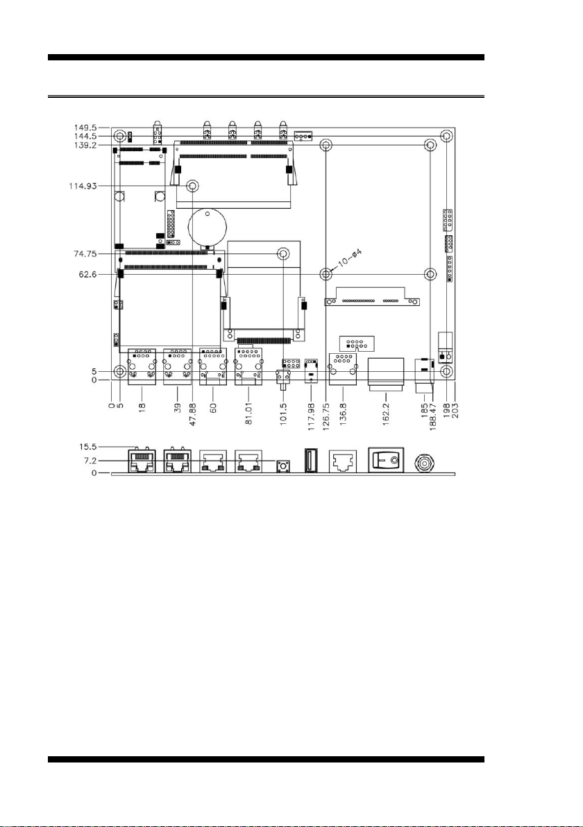
Board Dimensions
4
MB837-D25 / MB837-D25-R User’s Manual
Page 11

INSTALLATIONS
Installations
This section provides information on how to use the jumpers and connectors on
theMB837-D25 in order to set up a workable system. The topics covered are:
Installing the Memory ............................................................................ 6
Setting the Jumpers ................................................................................ 7
Setting the Connectors ......................................................................... 10
MB837-D25 / MB837-D25-R User’s Manual
5
Page 12
INSTALLATIONS
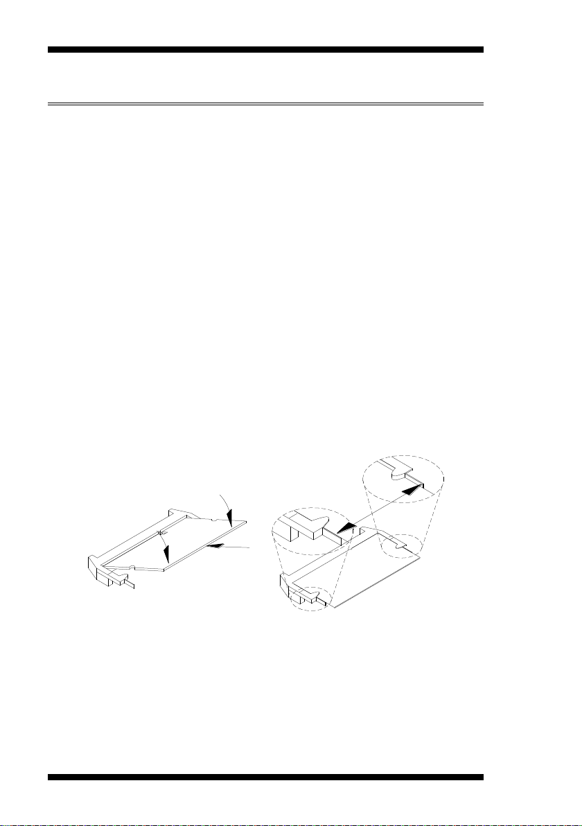
Installing the Memory
The MB837-D25 board supports one DDR3 memory socket that can support
up to 4GB memory, DDR3 1066/1333 (w/o ECC function).
Installing and Removing Memory Modules
To install the DDR3 module, locate the memory slot on the board and perform
the following steps:
1. Hold the DDR3 module so that the key of the DDR3 module aligns with that
on the memory slot. Insert the module into the socket at a slight angle
(approximately 30 degrees). Note that the socket and module are both keyed,
which means that the module can be installed only in one direction.
2. To seat the memory module into the socket, apply firm and even pressure to
each end of the module until you feel it slip down into the socket.
3. With the module properly seated in the socket, rotate the module downward.
Continue pressing downward until the clips at each end lock into position.
4. To remove the DDR3 module, press the clips with both hands.
6
MB837-D25 / MB837-D25-R User’s Manual
Page 13

INSTALLATIONS
Setting the Jumpers
Jumpers are used on MB837-D25 to select various settings and features
according to your needs and applications. Contact your supplier if you have
doubts about the best configuration for your needs. The following lists the
connectors on MB837-D25 and their respective functions.
JP1: Clear CMOS Contents ................................................................... 8
JP4, JP5: LAN Bypass & WDT Reboot Setting .................................... 9
MB837-D25 / MB837-D25-R User’s Manual
7
Page 14
INSTALLATIONS
JP1
Setting
Function
Pin 1-2
Short/Closed
Normal
Pin 2-3
Short/Closed
Clear CMOS
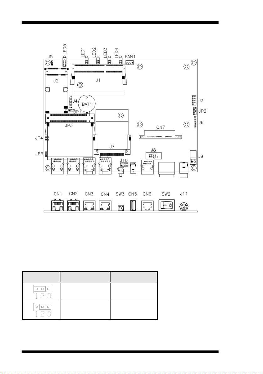
Jumper & Connector Location on MB837-D25 / MB837-D25-R
JP1: Clear CMOS Contents
Use JP1 to clear the CMOS contents.
Note that the power connector or jack should be disconnected from the board
before clearing CMOS.
8
MB837-D25 / MB837-D25-R User’s Manual
Page 15
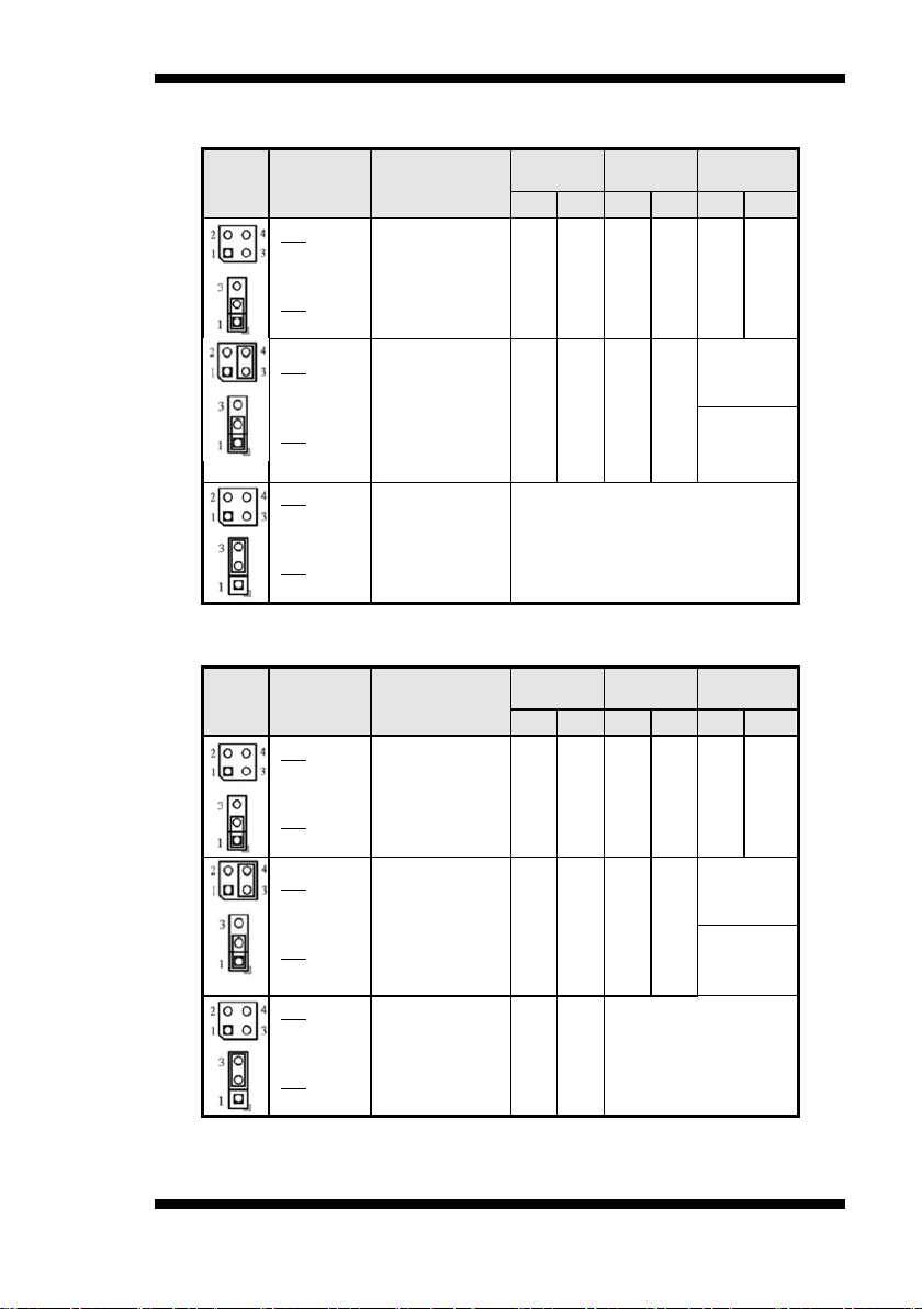
JP4, JP5: LAN Bypass & WDT Reboot Setting
JP4
JP5
Setting
Function
Power
OFF
Power
ON
Power ON
OS run software
Normal
Bypass
Normal
Bypass
Normal
Bypass
JP4
1-2 & 3-4
Open
JP5
1-2 Closed
LAN bypass
upon the time out
of WDT.
JP4
3-4 Closed
1-2 Open
JP5
1-2 Closed
LAN bypass &
system reboot
upon the time out
of WDT.
LAN
Always
Normal
WDT
Reboot
System
JP4
1-2 & 3-4
Open
JP5
2-3 Closed
LAN bypass
controlled by
Super IO GP54
or setting in
BIOS.
BIOS Setting **
GP54 Active:
Low: Bypass
High: Normal
JP4
JP5
Setting
Function
Power
OFF
Power
ON
Power ON
OS run software
Normal
Bypass
Normal
Bypass
Normal
Bypass
JP4
1-2 & 3-4
Open
JP5
1-2 Closed
LAN bypass
upon the time out
of WDT.
JP4
3-4 Closed
1-2 Open
JP5
1-2 Closed
LAN bypass &
system reboot
upon the time out
of WDT.
LAN
Always
Normal
WDT
Reboot
System
JP4
1-2 & 3-4
Open
JP5
2-3 Closed
LAN bypass
controlled by
Super IO GP54
or setting in
BIOS.
BIOS Setting **
GP54 Active:
Low: Bypass
High: Normal
Default Setting
Default Setting
MB837-D25
MB837-D25-R
INSTALLATIONS
** Note that the Bypass setting in BIOS is only working when JP4 & JP5 are
set as this configuration.
MB837-D25 / MB837-D25-R User’s Manual
9
Page 16

INSTALLATIONS
Setting the Connectors
FAN1: System Fan Power Connector .................................................. 11
CN1, CN2, CN3, CN4: 10 / 100 / 1000 LAN Ports ............................. 11
CN5: USB Connector .......................................................................... 11
CN6: COM1 RJ45 Connector .............................................................. 11
CN7: SATA HDD Dock ...................................................................... 12
J1: SO-DIMM DDR3 Socket ............................................................... 12
J2: Mini PCI-e Connector (USB signal only) ...................................... 12
J3: SPI Debug Port (Factory use only) ................................................. 12
J4: VGA Header ................................................................................... 12
J7: Slim Type II Compact Flash Connector ......................................... 13
J8: COM2 Serial Port ........................................................................... 13
J9: AT_12V Connector ........................................................................ 13
J10: USB Header ................................................................................. 13
J11: DC Power Jack (+12V only) ........................................................ 14
LED1, LED2, LED3 & LED4: LAN Port Link, Active LEDs ............. 14
LED5: Power, Alarm & Status LEDs................................................... 14
SW3: Software Reset Button ............................................................... 14
SW2: Power Switch ............................................................................. 14
JP3: Mini-PCI Connector ................................................................ ..... 14
10
MB837-D25 / MB837-D25-R User’s Manual
Page 17

INSTALLATIONS
Pin #
Signal Name
1
Ground
2
+12V
3
Rotation detection
4
Control
Pin #
Signal Name (RS-232)
1
RTS, Request to send
2
DTR, Data terminal ready
3
TXD, Transmit data
4
Ground
5
Ground
6
RXD, Receive data
7
DSR, Data set ready
8
CTS, Clear to send
FAN1: System Fan Power Connector
FAN1 is 4-pin header for System fan power. The fan must be a 12V fan.
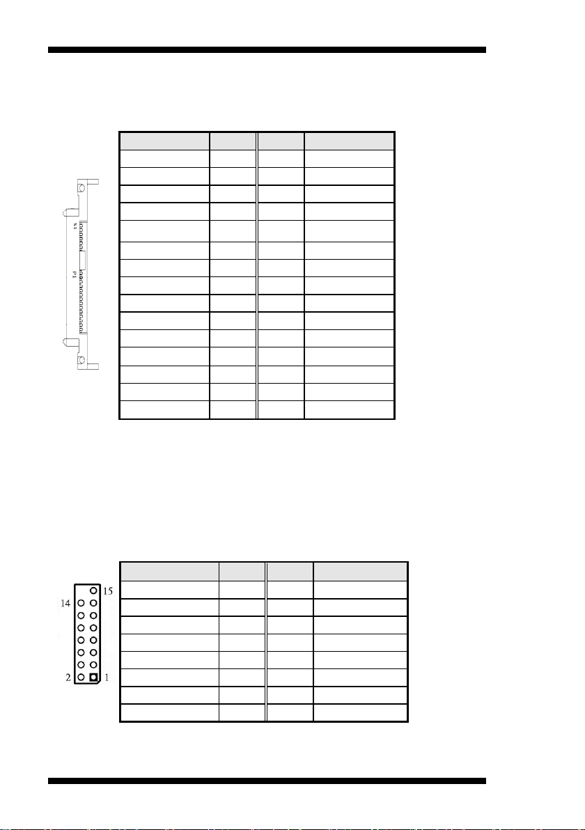
CN1, CN2, CN3, CN4: 10 / 100 / 1000 LAN Ports
CN5: USB Connector
CN6: COM1 RJ45 Connector
MB837-D25 / MB837-D25-R User’s Manual
11
Page 18
INSTALLATIONS
Signal Name
Pin #
Pin #
Signal Name
GND
S1
P1
+3.3V
A+
S2
P2
+3.3V
A-
S3
P3
+3.3V
GND
S4
P4
GND
B+
S5
P5
GND
B-
S6
P6
GND
GND
S7
P7
+5V
P8
+5V
P9
+5V
P10
GND
P11
GND
P12
GND
P13
+12V
P14
+12V
P15
+12V
Signal Name
Pin #
Pin #
Signal Name
DACR
1 2 +5VCRT
DACG
3 4 GND
DACB
5 6 NC
NC
7 8 CRT_SPD
GND
9
10
HSYNC_C
+5VCRT
11
12
VSYNC_C
GND
13
14
CRT_SPCLK
GND
15
CN7: SATA HDD Dock
The SATA HDD dock combines a SATA power connector and a SATA
interface connector.
J1: SO-DIMM DDR3 Socket
J2: Mini PCI-e Connector (USB signal only)
J3: SPI Debug Port (Factory use only)
J4: VGA Header
12
MB837-D25 / MB837-D25-R User’s Manual
Page 19
Pin #
Signal Name
1
KBDATA
2
KBCLK
3
MSDATA
4
MSCLK
5
GND
6
+5V
Pin #
Signal Name (RS-232)
1
DCD, Data carrier detect
2
RXD, Receive data
3
TXD, Transmit data
4
DTR, Data terminal ready
5
Ground
6
DSR, Data set ready
7
RTS, Request to send
8
CTS, Clear to send
9
RI, Ring indicator
10
No Connect.
Pin #
Signal Name
1
+12V
2
Ground
Signal Name
Pin #
Pin #
Signal Name
VCC
1 2 Ground
USB1-
3 4 USB2+
USB1+
5 6 USB2-
Ground
7 8 VCC
J6:PS2 KB/MS Header
J7: Slim Type II Compact Flash Connector
J8: COM2 Serial Port
INSTALLATIONS
J9: AT_12V Connector
J9 is a DC-in internal connector supporting +12V.
Note: Do not connect J9 and J11 at the same time.
J10: USB Header
MB837-D25 / MB837-D25-R User’s Manual
13
Page 20

INSTALLATIONS
Signal
Name
Pin #
Pin #
Signal
Name
PWR
LED+
A1
C1
PWR LED-
ALARM
LED+
A2
C2
SIO GPIO55
STATUS
LED+
A3
C3
SIO
GPIO56
Signal Name
Pin #
Pin #
Signal Name
GND
1
2
Intel NM10 PCH
GPIO7
J11: DC Power Jack (+12V only)
Note: Do not connect J9 and J11 at the same time.
LED1, LED2, LED3 & LED4: LAN Port Link, Active LEDs
LED5: Power, Alarm & Status LEDs
Index port: 4E
Data port: 4F
Device: 08
30h bit1 = 1
E0h bit5, bit6 = 0
E1h bit5, bit6 (Control pin)
SW3: Software Reset Button
Note: SW3 is controlled by GPIO only.
SW2: Power Switch
JP3: Mini-PCI Connector
14
IO Base:
Read IO 0x500 and set bit 7 to “1” (Enabled GPIO function)
Read IO 0x504 and set bit 7 to “1” (GPIO act as GPI )
Read IO 0x50C and check the bit 7 (Control Pin)
MB837-D25 / MB837-D25-R User’s Manual
Page 21

BIOS Setup
BIOS Setup
This chapter describes the different settings available in the AMI BIOS that
comes with the board. The topics covered in this chapter are as follows:
BIOS Introduction ............................................................................... 16
BIOS Setup .......................................................................................... 16
Advanced Settings ............................................................................... 18
Chipset Settings ................................................................................... 27
Security Settings .................................................................................. 33
Save & Exit Settings ............................................................................ 34
MB837-D25 / MB837-D25-R User’s Manual
15
Page 22

BIOS Setup
BIOS Introduction
The BIOS (Basic Input/Output System) installed in your computer system’s
ROM supports Intel processors. The BIOS provides critical low-level support
for a standard device such as disk drives, serial ports and parallel ports. It also
password protection as well as special support for detailed fine-tuning of the
chipset controlling the entire system.
BIOS Setup
The BIOS provides a Setup utility program for specifying the system
configurations and settings. The BIOS ROM of the system stores the Setup
utility. When you turn on the computer, the BIOS is immediately activated.
Pressing the <Del> key immediately allows you to enter the Setup utility. If you
are a little bit late pressing the <Del> key, POST (Power On Self Test) will
continue with its test routines, thus preventing you from invoking the Setup. If
you still wish to enter Setup, restart the system by pressing the ”Reset” button
or simultaneously pressing the <Ctrl>, <Alt> and <Delete> keys. You can also
restart by turning the system Off and back On again. The following message
will appear on the screen:
Press <DEL> to Enter Setup
In general, you press the arrow keys to highlight items, <Enter> to select, the
<PgUp> and <PgDn> keys to change entries, <F1> for help and <Esc> to quit.
When you enter the Setup utility, the Main Menu screen will appear on the
screen. The Main Menu allows you to select from various setup functions and
exit choices.
16
MB837-D25 / MB837-D25-R User’s Manual
Page 23

Warning:
It is strongly recommended that you avoid making any
changes to the chipset defaults. These defaults have been
carefully chosen by both AMI and your system manufacturer
to provide the absolute maximum performance and
reliability. Changing the defaults could cause the system to
become unstable and crash in some cases.
System Date
Set the Date. Use Tab to switch between Data elements.
System Time
Set the Time. Use Tab to switch between Data elements.
BIOS Setup
MB837-D25 / MB837-D25-R User’s Manual
17
Page 24

BIOS Setup
Main Advanced Chipset Boot Security Save & Exit
Legacy OpROM Support
→ ← Select Screen
↑↓ Select Item
Enter: Select
+- Change Field
F1: General Help
F2: Previous Values
F3: Optimized Default
F4: Save ESC: Exit
Launch PXE OpROM
Disabled
LAN Configuration State
Normal
► PCI Subsystem Settings
► ACPI Settings
► Wake up event setting
► CPU Configuration
► IDE Configuration
► USB Configuration
► W83627UHG Super IO Configuration
► H/W Monitor
► Serial Port Console Redirection
► PPM Configuration
Advanced Settings
This section allows you to configure and improve your system and allows you
to set up some system features according to your preference.
Launch PXE OpROM
Enable or Disable Boot Option for Legacy Network Devices.
LAN Configuration State
Enable (Bypass) or Disable (Normal) LAN Bypass. This function is only
working on GPIO control mode.
Refer to page 9 to set JP5 pin 2-3 closed.
Aptio Setup Utility
18
MB837-D25 / MB837-D25-R User’s Manual
Page 25

Main Advanced Chipset Boot Security Save & Exit
PCI Bus Driver Version V 2.05.01
→ ← Select Screen
↑↓ Select Item
Enter: Select
+- Change Field
F1: General Help
F2: Previous Values
F3: Optimized Default
F4: Save ESC: Exit
PCI Option ROM Handling
PCI ROM Priority
Legacy ROM
PCI Common Settings
PCI Latency Timer
32 PCI Bus Clocks
VGA Palette Snoop
Disabled
PERR# Generation
Disabled
SERR# Generation
Disabled
PCI Subsystem Settings
Aptio Setup Utility
PCI ROM Priority
In case of multiple Option ROMs (Legacy and EFI Compatible), specifies what
PCI Option ROM to launch.
PCI Latency Timer
Value to be programmed into PCI Latency Timer Register.
VGA Palette Snoop
Enables or Disables VGA Palette Registers Snooping.
PERR# Generation
Enables or Disables PCI Device to Generate PERR#.
SERR# Generation
Enables or Disables PCI Device to Generate SERR#.
MB837-D25 / MB837-D25-R User’s Manual
19
BIOS Setup
Page 26

BIOS Setup
Main Advanced Chipset Boot Security Save & Exit
ACPI Settings
Enable ACPI Auto Configuration Disabled
→ ← Select Screen
↑↓ Select Item
Enter: Select
+- Change Field
F1: General Help
F2: Previous Values
F3: Optimized Default
F4: Save ESC: Exit
Enable Hibernation
Enabled
ACPI Sleep State
S3 (Suspend to RAM)
Lock Legacy Resources
Disabled
S3 Video Report
Disabled
ACPI Settings
Aptio Setup Utility
Enabled ACPI Auto Configuration
Enables or Disables BIOS ACPI Auto Configuration.
Enable Hibernation
Enables or Disables System ability to Hibernate (OS/S4 Sleep State). This
option may be not effective with some OS.
ACPI Sleep State
Select the highest ACPI sleep state the system will enter, when the SUSPEND
button is pressed.
Lock Legacy Resources
Enables or Disables Lock of Legacy Resources.
S3 Video Report
Enable or Disable S3 Video Repost.
20
MB837-D25 / MB837-D25-R User’s Manual
Page 27

BIOS Setup
Main Advanced Chipset Boot Security Save & Exit
→ ← Select Screen
↑↓ Select Item
Enter: Select
+- Change Field
F1: General Help
F2: Previous Values
F3: Optimized Default
F4: Save ESC: Exit
Wake System with Fixed Time
Disabled
Wake on Ring
Disabled
Wake on PCIE PME
Disabled
Wake up event settings
Aptio Setup Utility
Wake System with Fixed Time
Enabled or Disabled System wake on alarm event. When enabled ,System will
wake on the hr : min : sec specified.
Wake on Ring
The options are Disabled and Enabled.
Wake on PCIE PME
The options are Disabled and Enabled.
MB837-D25 / MB837-D25-R User’s Manual
21
Page 28

BIOS Setup
Main Advanced Chipset Boot Security Save & Exit
CPU Configuration
→ ← Select Screen
↑↓ Select Item
Enter: Select
+- Change Field
F1: General Help
F2: Previous Values
F3: Optimized Default
F4: Save ESC: Exit
Processor Type
Intel(R) Atom(TM) CPU
EMT64
Not Supported
Processor Speed
1865 MHz
System Bus Speed
533 MHz
Ratio Status
14
Actual Ratio
14
System Bus Speed
533 MHz
Processor Stepping
30661
Microcode Revision
265
L1 Cache RAM
2x56 k
L2 Cache RAM
2x512 k
Processor Core
Dual
Hyper-Threading
Supported
Hyper-Threading
Enabled
Execute Disable Bit
Enabled
Limit CPUID Maximum
Disabled
CPU Configuration
This section shows the CPU configuration parameters.
Aptio Setup Utility
Hyper-threading
Enabled for Windows XP and Linux (OS optimized for Hyper-Threading
Technology) and Disabled for other OS (OS not optimized for
Hyper-Threading Technology). When Disabled, only one thread per enabled
core is enabled.
Execute Disable Bit
XD can prevent certain classes of malicious buffer overflow attacks when
combined with a supporting OS (Windows Server 2003 SP1, Windows XP
SP2, SuSE Linux 9.2, Re33dHat Enterprise 3 Update 3.)
Limit CPUID Maximum
Disabled for Windows XP.
22
MB837-D25 / MB837-D25-R User’s Manual
Page 29

Main Advanced Chipset Boot Security Save & Exit
→ ← Select Screen
↑↓ Select Item
Enter: Select
+- Change Field
F1: General Help
F2: Previous Values
F3: Optimized Default
F4: Save ESC: Exit
SATA Port0
Not Present
SATA Port1
Not Present
SATA Controller (s)
Enabled
Configure SATA as
IDE
IDE Configuration
Aptio Setup Utility
SATA Controller(s)
Enable / Disable Serial ATA Controller.
Configure SATA as
(1) IDE Mode.
(2) AHCI Mode.
BIOS Setup
MB837-D25 / MB837-D25-R User’s Manual
23
Page 30

BIOS Setup
Main Advanced Chipset Boot Security Save & Exit
USB Configuration
→ ← Select Screen
↑↓ Select Item
Enter: Select
+- Change Field
F1: General Help
F2: Previous Values
F3: Optimized Default
F4: Save ESC: Exit
USB Devices:
None
Legacy USB Support
Enabled
EHCI Hand-off
Enabled
USB hardware delays and time-outs:
USB Transfer time-out
20 sec
Device reset tine-out
20 sec
Device power-up delay
AUTO
USB Configuration
Aptio Setup Utility
Legacy USB Support
Enables Legacy USB support.
AUTO option disables legacy support if no USB devices are connected.
DISABLE option will keep USB devices available only for EFI applications.
EHCI Hand-off
Enabled/Disabled. This is a workaround for OSes without EHCI hand-off
support. The EHCI ownership change should be claimed by EHCI driver.
USB Transfer time-out
The time-out value for Control, Bulk, and Interrupt transfers.
Device reset tine-out
USB mass Storage device start Unit command time-out.
Device power-up delay
Maximum time the device will take before it properly reports itself to the Host
Controller. ‘Auto’ uses default value: for a Root port it is 100ms, for a Hub port
the delay is taken from Hub descriptor.
24
MB837-D25 / MB837-D25-R User’s Manual
Page 31

BIOS Setup
Main Advanced Chipset Boot Security Save & Exit
W83627UHG Super IO Configuration
→ ← Select Screen
↑↓ Select Item
Enter: Select
+- Change Field
F1: General Help
F2: Previous Values
F3: Optimized Default
F4: Save ESC: Exit
Super IO Chip
Winbond W83627UHG
► W83627UHG Serial Port 0 Configuration
► W83627UHG Serial Port 1 Configuration
Main Advanced Chipset Boot Security Save & Exit
→ ← Select Screen
↑↓ Select Item
Enter: Select
+- Change Field
F1: General Help
F2: Previous Values
F3: Optimized Default
F4: Save ESC: Exit
System temperature
+33 C
CPU temperature
System Fan Speed
+37 C
N/A
VCORE
+1.184 V
+12V
+11.904 V
+3.3V
+3.312 V
+1.05
+1.040 V
+5V
VBAT
+4.896 V
+3.168 V
CPU Shutdown Temperature
Disabled
SmartFan Control
Disabled
W83627UHG Super IO Configuration
Aptio Setup Utility
Serial Port Configuration
Set Parameters of Serial Ports. User can Enable/Disable the serial port and
Select an optimal settings for the Super IO Device.
H/W Monitor
Aptio Setup Utility
CPU Smart Fan Control
Disabled (default)
70 ℃
75 ℃
80 ℃
85 ℃
90 ℃
95 ℃
MB837-D25 / MB837-D25-R User’s Manual
25
Page 32

BIOS Setup
Main Advanced Chipset Boot Security Save & Exit
COM0
→ ← Select Screen
↑↓ Select Item
Enter: Select
+- Change Field
F1: General Help
F2: Previous Values
F3: Optimized Default
F4: Save ESC: Exit
Console Redirection
►Console Redirection Setting
Serial Port for Out-of Band Management /
Windows Emergency Management Services (EMS)
Enabled
Console Redirection
►Console Redirection Settings
Disabled
Main Advanced Chipset Boot Security Save & Exit
PPM Configuration
→ ← Select Screen
↑↓ Select Item
Enter: Select
+- Change Field
F1: General Help
F2: Previous Values
F3: Optimized Default
F4: Save ESC: Exit
EIST
Enabled
Temperatures/Voltages
These fields are the parameters of the hardware monitoring function feature of
the motherboard. The values are read-only values as monitored by the system
and show the PC health status.
CPU Shutdown Temperature
The default setting is disabled.
Serial Port Console Redirection
Aptio Setup Utility
PPM Configuration
Aptio Setup Utility
26
MB837-D25 / MB837-D25-R User’s Manual
Page 33

BIOS Setup
Main Advanced Chipset Boot Security Save & Exit
→ ← Select Screen
↑↓ Select Item
Enter: Select
+- Change Field
F1: General Help
F2: Previous Values
F3: Optimized Default
F4: Save ESC: Exit
► Host Bridge
► South Bridge
Chipset Settings
This section allows you to configure and improve your system and allows you
to set up some system features according to your preference.
Host Bridge
This item shows the Host Bridge Parameters.
South Bridge
This item shows the South Bridge Parameters.
Aptio Setup Utility
MB837-D25 / MB837-D25-R User’s Manual
27
Page 34

BIOS Setup
Main Advanced Chipset Boot Security Save & Exit
→ ← Select Screen
↑↓ Select Item
Enter: Select
+- Change Field
F1: General Help
F2: Previous Values
F3: Optimized Default
F4: Save ESC: Exit
► Memory Frequency and Timing
************Memory Information************
Memory Frequency
1067 MHz (DDR3)
Total Memory
2048 MB
DIMM#1
2048 MB
Main Advanced Chipset Boot Security Save & Exit
Memory Frequency and Timing
→ ← Select Screen
↑↓ Select Item
Enter: Select
+- Change Field
F1: General Help
F2: Previous Values
F3: Optimized Default
F4: Save & Exit
ESC: Exit
MRC Fast Boot
Enabled
Max TOLUD
Dynamic
Host Bridge
This section allows you to configure the Host Bridge Chipset.
Aptio Setup Utility
Memory Frequency and Timing
Aptio Setup Utility
MRC Fast Boot
The options are Disabled and Enabled.
Max TOLUD
Maximum Value of TOLUD. Dynamic assignment would adjust TOLUD
automatically based on largest MMIO length of installed graphic controller.
28
MB837-D25 / MB837-D25-R User’s Manual
Page 35

BIOS Setup
Main Advanced Chipset Boot Security Save & Exit
→ ← Select Screen
↑↓ Select Item
Enter: Select
+- Change Field
F1: General Help
F2: Previous Values
F3: Optimized Default
F4: Save ESC: Exit
► TPT Device
► PCI Express Root Port0
► PCI Express Root Port1
► PCI Express Root Port2
► PCI Express Root Port3
DMI Link ASPM Control
Enabled
PCI-Exp. High Priority Port
Disabled
High Precision Event Timer Configuration
High Precision Timer
Enabled
SLP_SP4 Assertion Width
1-2 Seconds
South Bridge
This section allows you to configure the South Bridge Chipset.
Aptio Setup Utility
DMI Clink ASPM Control
The control of Active State Power Management on both NB side and SB side of
the DMI Link.
PCI-Exp. High Priority Port
The options are Disabled, Port1, Port2, Port3, and Port4.
High Precision Event Timer Configuration
Enable/or Disable the High Precision Event Timer.
SLP_S4 Assertion Stretch Enable
Select a minimum assertion width of the SLP_S4# signal.
MB837-D25 / MB837-D25-R User’s Manual
29
Page 36

BIOS Setup
Main Advanced Chipset Boot Security Save & Exit
→ ← Select Screen
↑↓ Select Item
Enter: Select
+- Change Field
F1: General Help
F2: Previous Values
F3: Optimized Default
F4: Save ESC: Exit
Select USB Mode
By Controllers
UHCI #1 (port 0 and 1)
Enabled
UHCI #2 (port 2 and 3)
Enabled
UHCI #3 (port 4 and 5)
Enabled
UHCI #4 (port 6 and 7)
Enabled
USB 2.0 (EHCI) Support
Enabled
Main Advanced Chipset Boot Security Save & Exit
→ ← Select Screen
↑↓ Select Item
Enter: Select
+- Change Field
F1: General Help
F2: Previous Values
F3: Optimized Default
F4: Save ESC: Exit
PCI Express Port 0
Enabled
Port 0 IOxAPIC
Disabled
Automatic ASPM
Manual
ASPM L0s
Root Port Only
ASPM L1
Enabled
Main Advanced Chipset Boot Security Save & Exit
→ ← Select Screen
↑↓ Select Item
Enter: Select
+- Change Field
F1: General Help
F2: Previous Values
F3: Optimized Default
F4: Save ESC: Exit
PCI Express Port 1
Auto
Port 0 IOxAPIC
Disabled
Automatic ASPM
Manual
ASPM L0s
Root Port Only
ASPM L1
Enabled
TPT Device
PCI Express Root Port0
Aptio Setup Utility
Aptio Setup Utility
PCI Express Root Port1
Aptio Setup Utility
30
MB837-D25 / MB837-D25-R User’s Manual
Page 37

Main Advanced Chipset Boot Security Save & Exit
→ ← Select Screen
↑↓ Select Item
Enter: Select
+- Change Field
F1: General Help
F2: Previous Values
F3: Optimized Default
F4: Save ESC: Exit
PCI Express Port 2
Auto
Port 0 IOxAPIC
Disabled
Automatic ASPM
Manual
ASPM L0s
Root Port Only
ASPM L1
Enabled
Main Advanced Chipset Boot Security Save & Exit
→ ← Select Screen
↑↓ Select Item
Enter: Select
+- Change Field
F1: General Help
F2: Previous Values
F3: Optimized Default
F4: Save ESC: Exit
PCI Express Port 3
Auto
Port 0 IOxAPIC
Disabled
Automatic ASPM
Manual
ASPM L0s
Root Port Only
ASPM L1
Enabled
PCI Express Root Port2
PCI Express Root Port3
BIOS Setup
Aptio Setup Utility
Aptio Setup Utility
MB837-D25 / MB837-D25-R User’s Manual
31
Page 38

BIOS Setup
Main Advanced Chipset Boot Security Save & Exit
Boot Configuration
→ ← Select Screen
↑↓ Select Item
Enter: Select
+- Change Field
F1: General Help
F2: Previous Values
F3: Optimized Default
F4: Save ESC: Exit
Setup Prompt Timeout
1
Bootup NumLock State
On
Quiet Boot
Disabled
Fast Boot
Disabled
CSM16 Module Version
07.68
GateA20 Active
Upon Request
Option ROM Messages
Force BIOS
Interrupt 19 Capture
Enabled
CSM Support
Enabled
Boot Option Priorities
Boot Settings
Aptio Setup Utility
Setup Prompt Timeout
Number of seconds to wait for setup activation key.
65535(0xFFFF) means indefinite waiting.
Bootup NumLock State
Select the keyboard NumLock state.
Quiet Boot
Enables/Disables Quiet Boot option.
Fast Boot
Enables/Disables boot with initialization of a minimal set of devices to launch
active boot option. Has no effect for BBS boot options.
GateA20 Active
UPON REQUEST – GA20 can be disabled using BIOS services.
ALWAYS – do not allow disabling GA20; this option is useful when any RT
code is executed above 1MB.
Option ROM Messages
Set display mode. Options: Force BIOS and Keep Current.
Interrupt 19 Capture
Enable: Allows Option ROMs to trap Int 19.
CSM Support
Enables/Disables/Auto CSM Support.
32
MB837-D25 / MB837-D25-R User’s Manual
Page 39

BIOS Setup
Main Advanced Chipset Boot Security Save & Exit
Password Description
→ ← Select Screen
↑↓ Select Item
Enter: Select
+- Change Field
F1: General Help
F2: Previous Values
F3: Optimized Default
F4: Save ESC: Exit
If ONLY the Administrator’s password is set,
then this only limits access to Setup and is
only asked for when entering Setup.
If ONLY the User’s password is set, then this
is a power on password and must be entered to
boot or enter Setup. In Setup the User will
have Administrator rights.
The password length must be
in the following range:
Minimum length
Maximum length
3
20
Administrator Password
User Password
Boot Option Priorities
Sets the system boot order.
Security Settings
This section allows you to configure and improve your system and allows you
to set up some system features according to your preference.
Aptio Setup Utility
Administrator Password
Set Setup Administrator Password.
User Password
Set User Password.
MB837-D25 / MB837-D25-R User’s Manual
33
Page 40

BIOS Setup
Main Advanced Chipset Boot Security Save & Exit
Save Changes and Exit
→ ← Select Screen
↑↓ Select Item
Enter: Select
+- Change Field
F1: General Help
F2: Previous Values
F3: Optimized Default
F4: Save ESC: Exit
Discard Changes and Exit
Save Changes and Reset
Discard Changes and Reset
Save Options
Save Changes
Discard Changes
Restore Defaults
Save as User Defaults
Restore User Defaults
Boot Override
Save & Exit Settings
Save Changes and Exit
Exit system setup after saving the changes.
Discard Changes and Exit
Exit system setup without saving any changes.
Save Changes and Reset
Reset the system after saving the changes.
Discard Changes and Reset
Reset system setup without saving any changes.
Save Changes
Save Changes done so far to any of the setup options.
Discard Changes
Discard Changes done so far to any of the setup options.
Restore Defaults
Restore/Load Defaults values for all the setup options.
34
MB837-D25 / MB837-D25-R User’s Manual
Aptio Setup Utility
Page 41

Save as User Defaults
Save the changes done so far as User Defaults.
Restore User Defaults
Restore the User Defaults to all the setup options.
Boot Override
Pressing ENTER causes the system to enter the OS.
BIOS Setup
MB837-D25 / MB837-D25-R User’s Manual
35
Page 42

BIOS Setup
This page is intentionally left blank.
36
MB837-D25 / MB837-D25-R User’s Manual
Page 43

DRIVERS INSTALLATION
Drivers Installation
This section describes the installation procedures for software and drivers. The
software and drivers are included with the motherboard. If you find the items
missing, please contact the vendor where you made the purchase. The contents
of this section include the following:
Intel Chipset Software Installation Utility ........................................... 38
VGA Drivers Installation ..................................................................... 39
LAN Drivers Installation ..................................................................... 41
IMPORTANT NOTE:
After installing your Windows operating system, you must install first the Intel
Chipset Software Installation Utility before proceeding with the drivers
installation.
MB837-D25 / MB837-D25-R User’s Manual
37
Page 44
DRIVERS INSTALLATION
Intel Chipset Software Installation Utility
The Intel Chipset Drivers should be installed first before the software drivers to
enable Plug & Play INF support for Intel chipset components. Follow the
instructions below to complete the installation.
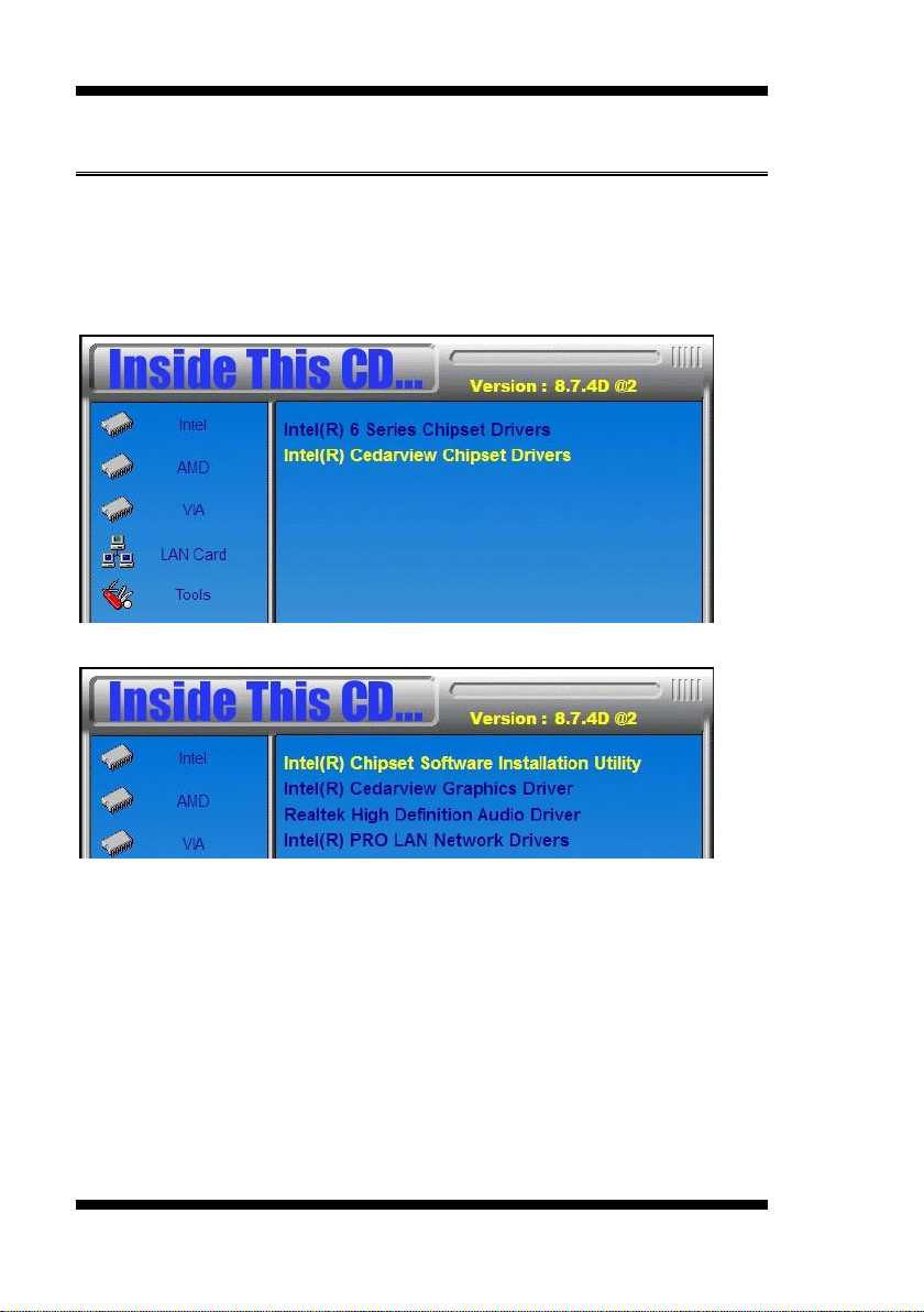
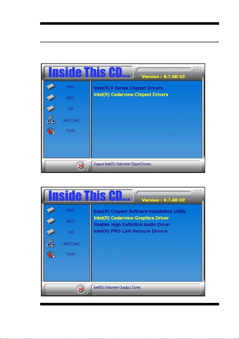
1. Insert the disc that comes with the board. Click Intel and then Intel(R)
Cedarview Chipset Drivers.
2. Click Intel(R) Chipset Software Installation Utility.
3. When the Welcome screen to the Intel® Chipset Device Software appears,
click Next to continue.
4. Click Yes to accept the software license agreement and proceed with the
installation process.
5. On the Readme File Information screen, click Next to continue the
installation.
6. The Setup process is now complete. Click Finish to restart the computer and
for changes to take effect.
38
MB837-D25 / MB837-D25-R User’s Manual
Page 45
DRIVERS INSTALLATION
VGA Drivers Installation
1. Insert the disc that comes with the board. Click Intel and then Intel(R)
Cedarview Chipset Drivers.
2. Click Intel(R) Cedarview Graphics Driver.
MB837-D25 / MB837-D25-R User’s Manual
39
Page 46

DRIVERS INSTALLATION
3. When the Welcome screen appears, click Next to continue.
4. Click Yes to to agree with the license agreement and continue the installation.
5. On the Readme File Information screen, click Next to continue the
installation of the Intel® Graphics Media Accelerator Driver.
6. On Setup Progress screen, click Next to continue.
7. Setup complete. Click Finish to restart the computer and for changes to take
effect.
40
MB837-D25 / MB837-D25-R User’s Manual
Page 47

LAN Drivers Installation
1. Insert the disc that comes with the board. Click LAN Card and then Intel
LAN Cedarview Drivers.
2. On the next screen, click Install Drivers and Software.
DRIVERS INSTALLATION
3. In the Welcome screen, click Next. On the next screen, click Yes to to agree
with the license agreement.
4. Agree with the license agreement and click Next.
MB837-D25 / MB837-D25-R User’s Manual
41
Page 48

DRIVERS INSTALLATION
5. Click the checkbox for Drivers in the Setup Options screen to select it and
click Next to continue.
6. The wizard is ready to begin installation. Click Install to begin the
installation.
7. When InstallShield Wizard is complete, click Finish.
42
MB837-D25 / MB837-D25-R User’s Manual
Page 49

Address
Device Description
000h - 01Fh
DMA Controller #1
020h - 03Fh
Interrupt Controller #1
040h - 05Fh
Timer
060h - 06Fh
Keyboard Controller
070h - 07Fh
Real Time Clock, NMI
080h - 09Fh
DMA Page Register
0A0h - 0BFh
Interrupt Controller #2
0C0h - 0DFh
DMA Controller #2
0F0h
Clear Math Coprocessor Busy Signal
0F1h
Reset Math Coprocessor
1F0h - 1F7h
IDE Interface
2F8h - 2FFh
Serial Port #2(COM2)
2B0h- 2DFh
Graphics adapter Controller
360h - 36Fh
Network Ports
3F8h - 3FFh
Serial Port #1(COM1)
APPENDIX
Appendix
A. I/O Port Address Map
Each peripheral device in the system is assigned a set of I/O port addresses
which also becomes the identity of the device. The following table lists the I/O
port addresses used.
MB837-D25 / MB837-D25-R User’s Manual
43
Page 50

APPENDIX
Level
Function
IRQ 0
System timer
IRQ 1
Standard PS/2 Keyboard
IRQ 3
Communications Port (COM2)
IRQ 4
Communications Port (COM1)
IRQ 5
Communications Port (COM3)
IRQ 7
Communications Port (COM4)
IRQ 8
System CMOS/real time clock
IRQ 11
Intel(R) N10/ICH7 Family SMBus Controller 27DA
IRQ 12
Microsoft PS/2 Mouse
IRQ 13
Numeric data processor
IRQ 16
Intel(R) N10/ICH7 Family USB Universal Host
Controller - 27CB
IRQ 18
Intel(R) N10/ICH7 Family USB Universal Host
Controller - 27CA
IRQ 19
Intel(R) N10/ICH7 Family Serial ATA Storage
Controller - 27C0
IRQ 19
Intel(R) N10/ICH7 Family USB Universal Host
Controller - 27C9
IRQ 22
High Definition Audio Controller
IRQ 23
Intel(R) N10/ICH7 Family USB2 Enhanced Host
Controller - 27CC
IRQ 23
Intel(R) N10/ICH7 Family USB Universal Host
Controller - 27C8
IRQ 4294967290
Intel(R) 82583V Gigabit Network Connection
IRQ 4294967291
Intel(R) 82583V Gigabit Network Connection #2
IRQ 4294967292
Intel(R) Graphics Media Accelerator 3600 Series
IRQ 4294967293
Intel(R) N10/ICH7 Family PCI Express Root Port 27D2
IRQ 4294967294
Intel(R) N10/ICH7 Family PCI Express Root Port 27D0
B. Interrupt Request Lines (IRQ)
Peripheral devices use interrupt request lines to notify CPU for the service
required. The following table shows the IRQ used by the devices on board.
44
MB837-D25 / MB837-D25-R User’s Manual
Page 51

APPENDIX
C. Watchdog Timer Configuration
The WDT is used to generate a variety of output signals after a user
programmable count. The WDT is suitable for use in the prevention of system
lock-up, such as when software becomes trapped in a deadlock. Under these
sorts of circumstances, the timer will count to zero and the selected outputs will
be driven. Under normal circumstance, the user will restart the WDT at regular
intervals before the timer counts to zero.
SAMPLE CODE:
File of the W627UHG.CPP
//--------------------------------------------------------------------------//
// THIS CODE AND INFORMATION IS PROVIDED "AS IS" WITHOUT WARRANTY OF ANY
// KIND, EITHER EXPRESSED OR IMPLIED, INCLUDING BUT NOT LIMITED TO THE
// IMPLIED WARRANTIES OF MERCHANTABILITY AND/OR FITNESS FOR A PARTICULAR
// PURPOSE.
//
//--------------------------------------------------------------------------#include "W627UHG.H"
#include <dos.h>
//--------------------------------------------------------------------------unsigned int W627UHG_BASE;
void Unlock_W627UHG (void);
void Lock_W627UHG (void);
//--------------------------------------------------------------------------unsigned int Init_W627UHG(void)
{
unsigned int result;
unsigned char ucDid;
W627UHG_BASE = 0x4E;
result = W627UHG_BASE;
ucDid = Get_W627UHG_Reg(0x20);
if (ucDid == 0xA2) //W83627UHG??
{ goto Init_Finish; }
W627UHG_BASE = 0x2E;
result = W627UHG_BASE;
ucDid = Get_W627UHG_Reg(0x20);
if (ucDid == 0xA2) //W83627UHG??
{ goto Init_Finish; }
W627UHG_BASE = 0x00;
result = W627UHG_BASE;
Init_Finish:
return (result);
MB837-D25 / MB837-D25-R User’s Manual
45
Page 52

APPENDIX
}
//--------------------------------------------------------------------------void Unlock_W627UHG (void)
46
MB837-D25 / MB837-D25-R User’s Manual
Page 53

{
outportb(W627UHG_INDEX_PORT, W627UHG_UNLOCK);
outportb(W627UHG_INDEX_PORT, W627UHG_UNLOCK);
}
//--------------------------------------------------------------------------void Lock_W627UHG (void)
{
outportb(W627UHG_INDEX_PORT, W627UHG_LOCK);
}
//--------------------------------------------------------------------------void Set_W627UHG_LD( unsigned char LD)
{
Unlock_W627UHG();
outportb(W627UHG_INDEX_PORT, W627UHG_REG_LD);
outportb(W627UHG_DATA_PORT, LD);
Lock_W627UHG();
}
//--------------------------------------------------------------------------void Set_W627UHG_Reg( unsigned char REG, unsigned char DATA)
{
Unlock_W627UHG();
outportb(W627UHG_INDEX_PORT, REG);
outportb(W627UHG_DATA_PORT, DATA);
Lock_W627UHG();
}
//--------------------------------------------------------------------------unsigned char Get_W627UHG_Reg(unsigned char REG)
{
unsigned char Result;
Unlock_W627UHG();
outportb(W627UHG_INDEX_PORT, REG);
Result = inportb(W627UHG_DATA_PORT);
Lock_W627UHG();
return Result;
}
//---------------------------------------------------------------------------
APPENDIX
MB837-D25 / MB837-D25-R User’s Manual
47
Page 54

APPENDIX
File of the W627UHG.H
//--------------------------------------------------------------------------//
// THIS CODE AND INFORMATION IS PROVIDED "AS IS" WITHOUT WARRANTY OF ANY
// KIND, EITHER EXPRESSED OR IMPLIED, INCLUDING BUT NOT LIMITED TO THE
// IMPLIED WARRANTIES OF MERCHANTABILITY AND/OR FITNESS FOR A PARTICULAR
// PURPOSE.
//
//--------------------------------------------------------------------------#ifndef __W627UHG_H
#define __W627UHG_H 1
//--------------------------------------------------------------------------#define W627UHG_INDEX_PORT (W627UHG_BASE)
#define W627UHG_DATA_PORT (W627UHG_BASE+1)
//--------------------------------------------------------------------------#define W627UHG_REG_LD 0x07
//--------------------------------------------------------------------------#define W627UHG_UNLOCK 0x87
#define W627UHG_LOCK 0xAA
//--------------------------------------------------------------------------unsigned int Init_W627UHG(void);
void Set_W627UHG_LD( unsigned char);
void Set_W627UHG_Reg( unsigned char, unsigned char);
unsigned char Get_W627UHG_Reg( unsigned char);
//--------------------------------------------------------------------------#endif //__W627UHG_H
48
MB837-D25 / MB837-D25-R User’s Manual
Page 55

APPENDIX
File of the MAIN.CPP
//--------------------------------------------------------------------------//
// THIS CODE AND INFORMATION IS PROVIDED "AS IS" WITHOUT WARRANTY OF ANY
// KIND, EITHER EXPRESSED OR IMPLIED, INCLUDING BUT NOT LIMITED TO THE
// IMPLIED WARRANTIES OF MERCHANTABILITY AND/OR FITNESS FOR A PARTICULAR
// PURPOSE.
//
//--------------------------------------------------------------------------#include <dos.h>
#include <conio.h>
#include <stdio.h>
#include <stdlib.h>
#include "W627UHG.H"
//--------------------------------------------------------------------------int main (void);
void WDTInitial(void);
void WDTEnable(unsigned char);
void WDTDisable(void);
//--------------------------------------------------------------------------int main (void)
{
char SIO;
SIO = Init_W627UHG();
if (SIO == 0)
{
............................................... printf("Can not detect Winbond 83627UHG, program abort.\n");
.................................................................................................................................... return(1);
}
WDTInitial();
WDTEnable(10);
WDTDisable();
return 0;
}
//--------------------------------------------------------------------------void WDTInitial(void)
{
unsigned char bBuf;
Set_W627UHG_LD(0x08); ................................................................. //switch to logic device 8
bBuf = Get_W627UHG_Reg(0x30);
bBuf &= (~0x01);
Set_W627UHG_Reg(0x30, bBuf); ................................................................... //Enable WDTO
}
//--------------------------------------------------------------------------void WDTEnable(unsigned char NewInterval)
{
unsigned char bBuf;
Set_W627UHG_LD(0x08); ................................................................. //switch to logic device 8
Set_W627UHG_Reg(0x30, 0x01); ....................................................................... //enable timer
MB837-D25 / MB837-D25-R User’s Manual
49
Page 56

APPENDIX
bBuf = Get_W627UHG_Reg(0xF5);
bBuf &= (~0x08);
Set_W627UHG_Reg(0xF5, bBuf); ......................................................... //count mode is second
Set_W627UHG_Reg(0xF6, NewInterval); ................................ .................................. //set timer
}
//--------------------------------------------------------------------------void WDTDisable(void)
{
Set_W627UHG_LD(0x08); ................................................................. //switch to logic device 8
Set_W627UHG_Reg(0xF6, 0x00); .......................................................... //clear watchdog timer
Set_W627UHG_Reg(0x30, 0x00); .............................................................. //watchdog disabled
}
//---------------------------------------------------------------------------
50
MB837-D25 / MB837-D25-R User’s Manual
Page 57

APPENDIX
D. Digital I/O Sample Code
File of the W627UHG.H
//--------------------------------------------------------------------------//
// THIS CODE AND INFORMATION IS PROVIDED "AS IS" WITHOUT WARRANTY OF ANY
// KIND, EITHER EXPRESSED OR IMPLIED, INCLUDING BUT NOT LIMITED TO THE
// IMPLIED WARRANTIES OF MERCHANTABILITY AND/OR FITNESS FOR A PARTICULAR
// PURPOSE.
//
//--------------------------------------------------------------------------#ifndef __W627UHG_H
#define __W627UHG_H 1
//--------------------------------------------------------------------------#define W627UHG_INDEX_PORT (W627UHG_BASE)
#define W627UHG_DATA_PORT (W627UHG_BASE+1)
//--------------------------------------------------------------------------#define W627UHG_REG_LD 0x07
//--------------------------------------------------------------------------#define W627UHG_UNLOCK 0x87
#define W627UHG_LOCK 0xAA
//--------------------------------------------------------------------------unsigned int Init_W627UHG(void);
void Set_W627UHG_LD( unsigned char);
void Set_W627UHG_Reg( unsigned char, unsigned char);
unsigned char Get_W627UHG_Reg( unsigned char);
//--------------------------------------------------------------------------#endif //__W627UHG_H
MB837-D25 / MB837-D25-R User’s Manual
51
Page 58

APPENDIX
File of the W627UHG.CPP
//--------------------------------------------------------------------------//
// THIS CODE AND INFORMATION IS PROVIDED "AS IS" WITHOUT WARRANTY OF ANY
// KIND, EITHER EXPRESSED OR IMPLIED, INCLUDING BUT NOT LIMITED TO THE
// IMPLIED WARRANTIES OF MERCHANTABILITY AND/OR FITNESS FOR A PARTICULAR
// PURPOSE.
//
//--------------------------------------------------------------------------#include "W627UHG.H"
#include <dos.h>
//--------------------------------------------------------------------------unsigned int W627UHG_BASE;
void Unlock_W627UHG (void);
void Lock_W627UHG (void);
//--------------------------------------------------------------------------unsigned int Init_W627UHG(void)
{
unsigned int result;
unsigned char ucDid;
W627UHG_BASE = 0x4E;
result = W627UHG_BASE;
ucDid = Get_W627UHG_Reg(0x20);
if (ucDid == 0xA2) //W83627UHG??
{ goto Init_Finish; }
W627UHG_BASE = 0x2E;
result = W627UHG_BASE;
ucDid = Get_W627UHG_Reg(0x20);
if (ucDid == 0xA2) //W83627UHG??
{ goto Init_Finish; }
W627UHG_BASE = 0x00;
result = W627UHG_BASE;
Init_Finish:
return (result);
}
//--------------------------------------------------------------------------void Unlock_W627UHG (void)
{
outportb(W627UHG_INDEX_PORT, W627UHG_UNLOCK);
outportb(W627UHG_INDEX_PORT, W627UHG_UNLOCK);
}
//--------------------------------------------------------------------------void Lock_W627UHG (void)
{
outportb(W627UHG_INDEX_PORT, W627UHG_LOCK);
}
//--------------------------------------------------------------------------void Set_W627UHG_LD( unsigned char LD)
52
MB837-D25 / MB837-D25-R User’s Manual
Page 59

{
Unlock_W627UHG();
outportb(W627UHG_INDEX_PORT, W627UHG_REG_LD);
outportb(W627UHG_DATA_PORT, LD);
Lock_W627UHG();
}
//--------------------------------------------------------------------------void Set_W627UHG_Reg( unsigned char REG, unsigned char DATA)
{
Unlock_W627UHG();
outportb(W627UHG_INDEX_PORT, REG);
outportb(W627UHG_DATA_PORT, DATA);
Lock_W627UHG();
}
//--------------------------------------------------------------------------unsigned char Get_W627UHG_Reg(unsigned char REG)
{
unsigned char Result;
Unlock_W627UHG();
outportb(W627UHG_INDEX_PORT, REG);
Result = inportb(W627UHG_DATA_PORT);
Lock_W627UHG();
return Result;
}
//---------------------------------------------------------------------------
APPENDIX
MB837-D25 / MB837-D25-R User’s Manual
53
Page 60

APPENDIX
File of the MAIN.CPP
//--------------------------------------------------------------------------//
// THIS CODE AND INFORMATION IS PROVIDED "AS IS" WITHOUT WARRANTY OF ANY
// KIND, EITHER EXPRESSED OR IMPLIED, INCLUDING BUT NOT LIMITED TO THE
// IMPLIED WARRANTIES OF MERCHANTABILITY AND/OR FITNESS FOR A PARTICULAR
// PURPOSE.
//
//--------------------------------------------------------------------------#include <dos.h>
#include <conio.h>
#include <stdio.h>
#include <stdlib.h>
#include "W627UHG.H"
//--------------------------------------------------------------------------int main (void);
void Dio5Initial(void);
void Dio5SetOutput(unsigned char);
unsigned char Dio5GetInput(void);
void Dio5SetDirection(unsigned char);
unsigned char Dio5GetDirection(void);
//--------------------------------------------------------------------------int main (void)
{
char SIO;
SIO = Init_W627UHG();
if (SIO == 0)
{
printf("Can not detect Winbond 83627UHG, program abort.\n");
return(1);
}
Dio5Initial();
//for GPIO50..57
Dio5SetDirection(0x0F); //GP50..53 = input, GP54..57=output
printf("Current DIO direction = 0x%X\n", Dio5GetDirection());
printf("Current DIO status = 0x%X\n", Dio5GetInput());
printf("Set DIO output to high\n");
Dio5SetOutput(0x0F);
printf("Set DIO output to low\n");
Dio5SetOutput(0x00);
return 0;
}
//--------------------------------------------------------------------------void Dio5Initial(void)
{
unsigned char ucBuf;
Set_W627UHG_LD(0x08); //switch to logic device 8
//enable the GP5 group
ucBuf = Get_W627UHG_Reg(0x30);
ucBuf |= 0x02;
54
MB837-D25 / MB837-D25-R User’s Manual
Page 61

Set_W627UHG_Reg(0x30, ucBuf);
}
//--------------------------------------------------------------------------void Dio5SetOutput(unsigned char NewData)
{
Set_W627UHG_LD(0x08); //switch to logic device 8
Set_W627UHG_Reg(0xE1, NewData);
}
//--------------------------------------------------------------------------unsigned char Dio5GetInput(void)
{
unsigned char result;
Set_W627UHG_LD(0x08); //switch to logic device 8
result = Get_W627UHG_Reg(0xE1);
return (result);
}
//--------------------------------------------------------------------------void Dio5SetDirection(unsigned char NewData)
{
//NewData : 1 for input, 0 for output
Set_W627UHG_LD(0x08); //switch to logic device 8
Set_W627UHG_Reg(0xE0, NewData);
}
//--------------------------------------------------------------------------unsigned char Dio5GetDirection(void)
{
unsigned char result;
Set_W627UHG_LD(0x08); //switch to logic device 8
result = Get_W627UHG_Reg(0xE0);
return (result);
}
//---------------------------------------------------------------------------
APPENDIX
MB837-D25 / MB837-D25-R User’s Manual
55
 Loading...