

Page 1

IB831
VIA VX900
5.25-inch Disk Size SBC
USER’S MANUAL
Version 1.0
Page 2

Acknowledgments
AMI is a registered trademark of American Megatrends Inc.
PS/2 is a trademark of International Business Machines
Corporation.
Microsoft Windows is a registered trademark of Microsoft
Corporation.
Winbond is a registered trademark of Winbond Electronics
Corporation.
All other product names or trademarks are properties of their
respective owners.
ii
IB831 User’s Manual
Page 3

Table of Contents
Introduction ............................................................. 1
Product Description ............................................................ 1
Checklist ............................................................................. 2
Specifications ..................................................................... 3
Board Dimensions .............................................................. 4
Installations ............................................................. 5
Installing the Memory......................................................... 6
Setting the Jumpers............................................................. 7
Connectors on IB831 .......................................................... 9
Bypass and WDT ............................................................. 15
Block Diagram: ................................................................ 15
Communication States: ..................................................... 15
Watchdog Timer Configuration ........................................ 16
GPIO Function Definition ................................................ 19
Digital I/O Sample Configuration ..................................... 20
BIOS Setup ............................................................. 25
Drivers Installation .................................................45
VIA VX900 VGA Driver Installation ............................... 46
Realtek LAN Driver Installation ....................................... 49
IB831 User’s Manual iii
Page 4

This page is intentionally left blank.
iv
IB831 User’s Manual
Page 5

INTRODUCTION
Model
VIA Nano
TM
X2
Dual Core CPU
LAN Bypass
Watchdog Timer
IB831
1.2 GHz
Yes
Yes
IB831-NB
1.2 GHz
No
Yes
Introduction
Product Description
The IB831 5.25-inch SBC incorporates the VIA VX900 chipset.
Currently, the board is available in three models, namely:
IB831 Features
Supports four Realtek 10/100/1000 LAN ports
Supports 1.2GHz VIA Nano
DDR3 SO-DIMM x 1, up to 2GB
Mini PCI-e (USB Signal) slot, Compact Flash socket
Optional Hardware LAN Bypass function on Eth1 & 2
TM
X2 U4300 processor
IB831 User’s Manual 1
Page 6

INTRODUCTION
Checklist
Your IB831 package should include the items listed below.
The IB831 VIA NanoTM X2 motherboard
1 CD containing chipset drivers and flash memory utility
Optional cables for VGA, KB/MS, Serial port, Serial ATA
2
IB831 User’s Manual
Page 7

Form Factor
Desktop / Table Top Networking Product
CPU
VIA NanoTM X2 U4300 Dual Core @ 1.2 GHz, 13W
x86 and x64 (64-bit) capability
Bus speeds up to 1066 MHz
Hardware Virtualization (VMX)
VIA Virtualization (VIA-VT)
Enhanced PowerSaver provides fastest performance state
switching
Multi-processor support: Dual processing (SMP)
MMX, SSE, SSE2, SSSE3 and SSE4.1 compatible instructions
Two large (64-KB each, 16-way) Level 1 caches per core
1 MB Level 2 victim cache (32-way) with ECC per core (2 MB
Total)
Two Large TLBs (196 entries each, 12-way)
Chipset
VIA VX900 FSB 400~800 MHz, 4.5W
1.2V Core Voltage
800 / 533 / 400 MHz FSB support
PCI-e Gen2
128 bit 2D Graphic Engine
Ethernet
controller
Onboard 4X Realtek RT8111E PCIe GbE with RJ45
Memory
Single channel DDR3 up to 1066MHz
SO-DIMM Socket x1
Network
4x Realtek RT8111E Gigabit LAN, optional Bypass
Network
Bypass
Up to One segments hardware Bypass (ETH 1 & 2)
Control by GPIO / Watchdog / Electrical Disconnect (Power Off)
Watchdog
Timer
Yes (256 segments, 0, 1, 2…255 sec/min)
Expansion Slot
Mini PCI-e Slot (USB Signal only)
Storage
Onboard CF Socket x1, SATA Connector x1
LED Indicators
Power (Green) / Status (Green) / Alarm (Red)
LAN: Speed 10Mbps: LED off
100Mbps: Green
1000Mbps: Amber
Link / ACT: Green / Green Blinking
Edge
Connectors
DC +12V inlet
RJ45 x4
DB-9 Console Port
USB 2.0 x2
USB 2.0
2 ports
VGA
Pin header on board
Power
DC-In +12V
Dimensions
203 (W) x 146 (D) mm
Specifications
INTRODUCTION
IB831 User’s Manual 3
Page 8
INTRODUCTION
Board Dimensions
203 (W) x 146 (D) mm
4
IB831 User’s Manual
Page 9

INSTALLATION
Installations
This section provides information on how to use the jumpers and
connectors on the IB831 in order to set up a workable system. The topics
covered are:
Installing the Memory ................................................................. 6
Setting the Jumpers .................................................................... 7
Connectors on IB831 .................................................................. 9
Bypass and WDT ...................................................................... 15
Block Diagram: ............................................................................... 15
Communication States:.................................................................... 15
Watchdog Timer Configuration ................................................ 16
GPIO Function Definition ......................................................... 19
Digital I/O Sample Configuration .............................................. 20
IB831 User’s Manual 5
Page 10

INSTALLATION
Installing the Memory
The IB831 board supports one DDR3 memory socket for a maximum
total memory of 2GB in DDR3 memory type.
Installing and Removing Memory Modules
To install the DDR3 modules, locate the memory slot on the board and
perform the following steps:
1. Hold the DDR3 module so that the key of the DDR3 module aligns
with those on the memory slot.
2. Gently push the DDR3 module in an upright position until the clips of
the slot close to hold the DDR3 module in place when the DDR3
module touches the bottom of the slot.
3. To remove the DDR3 module, press the clips with both hands.
6
IB831 User’s Manual
Page 11
INSTALLATION
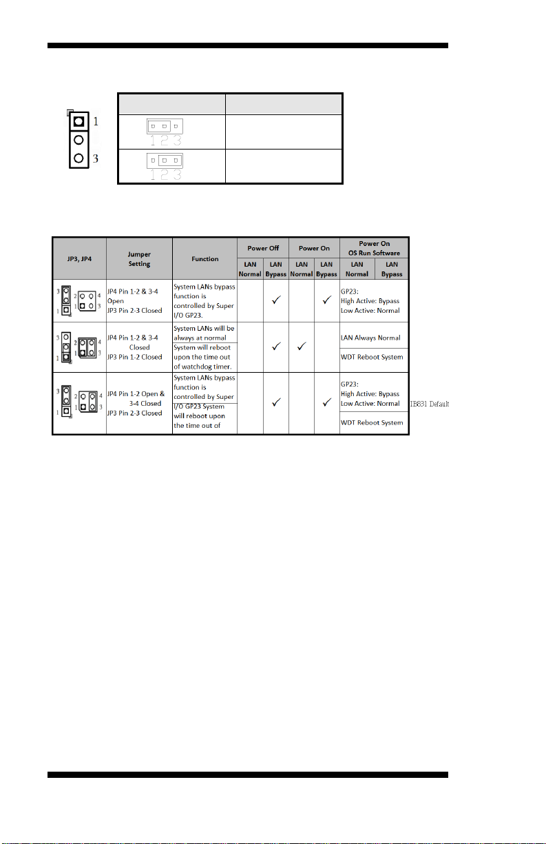
Setting the Jumpers
Jumpers are used on IB831 to select various settings and features
according to your needs and applications. Contact your supplier if you
have doubts about the best configuration for your needs.
Jumper Locations on IB831
Jumpers on IB831 ............................................................................ …7
J3: Clear CMOS Setting....................................................................... 8
JP3: LAN bypass controlled Setting ..................................................... 8
JP4: Bypass LANs & Reboot Setting ................................................... 8
IB831 User’s Manual 7
Page 12
INSTALLATION
J3
Setting
Normal
Clear CMOS
J3: Clear CMOS Setting
JP3 & JP4: Bypass LANs & Reboot Setting
8
IB831 User’s Manual
Page 13

INSTALLATION
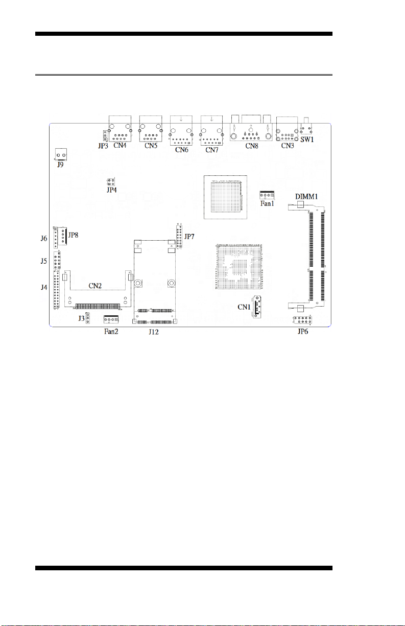
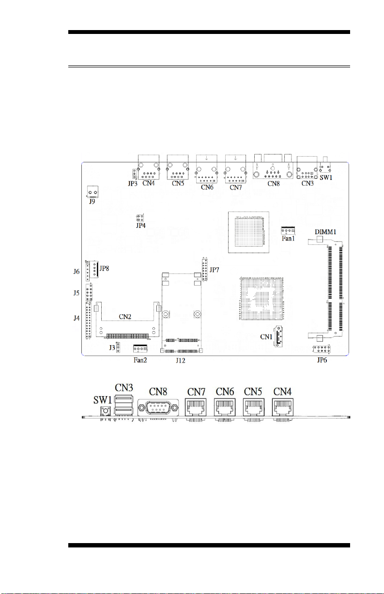
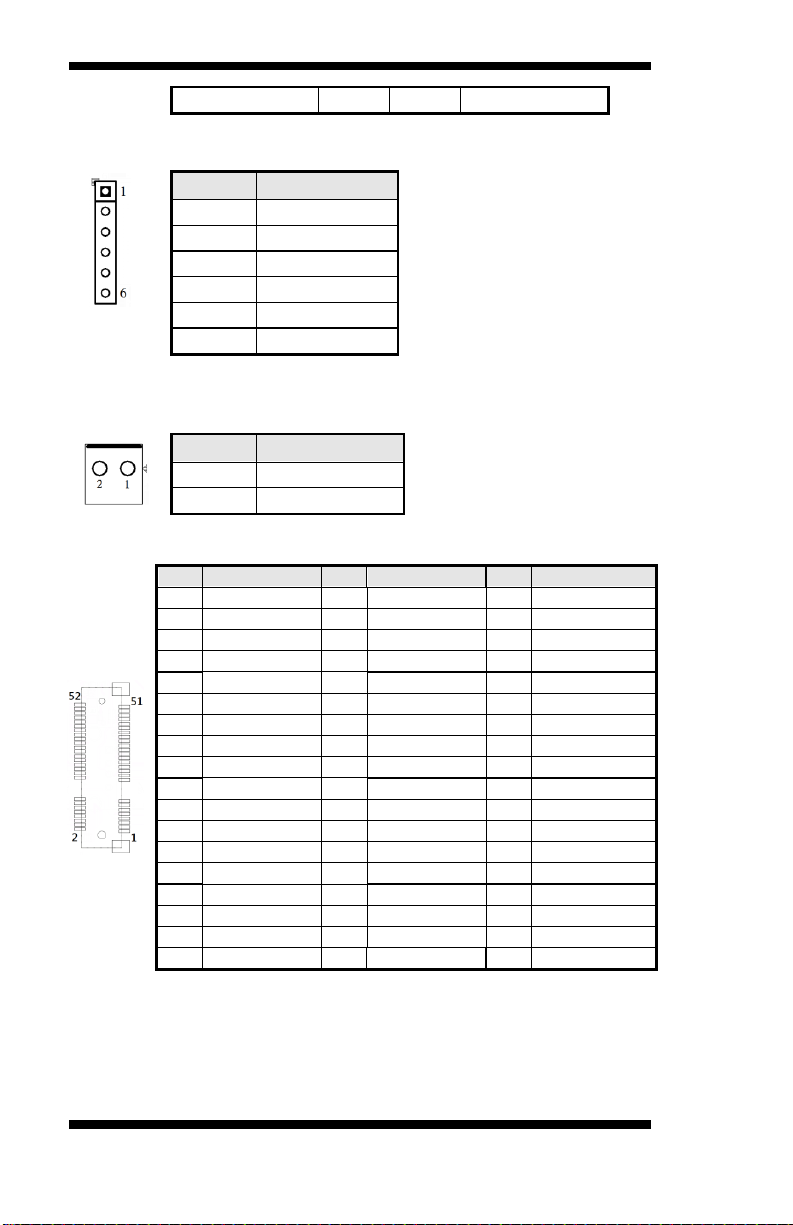
Connectors on IB831
The connectors on IB831 allow you to connect external devices such as
keyboard, floppy disk drives, hard disk drives, printers, etc. The following
table lists the connectors on IB831 and their respective functions.
FAN1: CPU Fan Power Connector .................. 錯誤! 尚未定義書籤。
FAN2: System Fan Power Connector ............... 錯誤! 尚未定義書籤。
CN3: USB1/2 Ports ......................................... 錯誤! 尚未定義書籤。
CN4, CN5: 10/100 /1000 RJ-45 Ports .............. 錯誤! 尚未定義書籤。
CN6, CN7: 10/100 /1000 RJ-45 Ports .............. 錯誤! 尚未定義書籤。
CN8: COM1 Serial Port ................................... 錯誤! 尚未定義書籤。
SW1: System Reset.......................................... 錯誤! 尚未定義書籤。
CN1: Serial ATA Port ..................................... 錯誤! 尚未定義書籤。
J4: Parallel Port ............................................... 錯誤! 尚未定義書籤。
J5: LPC Debug Port ......................................... 錯誤! 尚未定義書籤。
J6: PS/2 Keyboard and PS/2 Mouse Connectors錯誤! 尚未定義書籤。
J9: AT_12V Connector .................................... 錯誤! 尚未定義書籤。
J12: Mini PCI-E Connector (top side) .............. 錯誤! 尚未定義書籤。
JP6: SPI Debug Port ........................................ 錯誤! 尚未定義書籤。
JP7: VGA Connector ....................................... 錯誤! 尚未定義書籤。
JP8: HDD Power Connector (Output: Max. 2A)錯誤! 尚未定義書籤。
CN2: Compact Flash Connector (top side) ....... 錯誤! 尚未定義書籤。
IB831 User’s Manual 9
Page 14

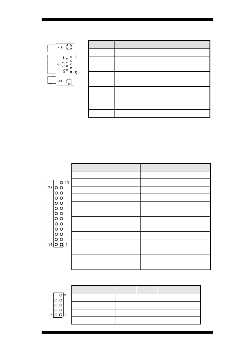
INSTALLATION
Pin #
Signal Name
1
Ground
2
+12V
3
Rotation detection
4 Rotation control
Pin #
Signal Name
1
Ground
2
+12V
3
Rotation detection
4 Rotation control
Signal Name
Pin #
Pin #
Signal Name
+5V
1 5 +5V
D-
2 6 D-
D+
3 7 D+
GND
4 8 GND
Signal Name
Pin #
Pin #
Signal Name
TX+
1 2 TX-
RX+
3 4 NC
NC
5 6 RX-
NC
7 8 NC
Signal Name
Pin #
Pin #
Signal Name
TX+
1 2 TX-
RX+
3 4 RX-
TCT
5 6 RCT
MDI2+
7 8 MDI2-
MDI3+
9
10
MDI3+
FAN1: CPU Fan Power Connector
FAN1 is a 4-pin header for the CPU fan. The fan must be 12V (Max. 1A).
FAN2: System Fan Power Connector
FAN2 is a 4-pin header for system fans. The fan must be 12V (Max. 1A).
CN3: USB1/2 Ports
CN4, CN5: 10/100 /1000 RJ-45 Ports
CN6, CN7: 10/100 /1000 RJ-45 Ports
10
IB831 User’s Manual
Page 15
Pin #
Signal Name
1
DCD, Data carrier detect
2
RXD, Receive data
3
TXD, Transmit data
4
DTR, Data terminal ready
5
Ground
6
DSR, Data set ready
7
RTS, Request to send
8
CTS, Clear to send
9
RI, Ring indicator
Signal Name
Pin #
Pin #
Signal Name
STB-
1
14
AFD-
PD0
2
15
ERR-
PD1
3
16
INIT-
PD2
4
17
SLIN-
PD3
5
18
Ground
PD4
6
19
Ground
PD5
7
20
Ground
PD6
8
21
Ground
PD7
9
22
Ground
ACK-
10
23
Ground
BUSY
11
24
Ground
PE
12
25
Ground
SLCT
13
Signal Name
Pin #
Pin #
Signal Name
LAD0
1 2 LRESET
LAD1
3 4 LFRAME#
LAD2
5 6 +3.3V
LAD3
7 8 Ground
CN8: COM1 Serial Port
SW1: System Reset
CN1: Serial ATA Port
J4: Parallel Port
INSTALLATION
J5: LPC Debug Port
IB831 User’s Manual 11
Page 16
INSTALLATION
PCI_CLK1
9
Pin #
Signal Name
1
KBDA
2
KBCL
3
MDA
4
MCL
5
Ground
6
+5VSUS
Pin #
Signal Name
1
+12V
2
Ground
Pin
Signal
Pin
Signal
Pin
Signal
1
WAKE#
19
RSVD4(UIM)
37
GND
2
+3.3Vaux
20
W_DISABLE
38
USB_D+
3
COEX1
21
GND
39
+3.3Vaux
4
GND
22
PERST#
40
GND
5
COEX2
23
PER_N0
41
+3.3Vaux
6
+1.5V
24
+3.3Vaux
42
LED_WWAN#
7
CLKREQ#
25
PER_P0
43
GND
8
UIM_PWR
26
GND
44
LED_WLAN#
9
GND
27
GND
45
RSVD9
10
UIM_DATA
28
+1.5V
46
LED_WPAN#
11
REFCLK-
29
GND
47
RSVD10
12
UIM_CLK
30
SMB_CLK
48
+1.5V
13
REFCLK+
31
PET_N0
49
RSVD11
14
UIM_RESET
32
SMB_DATA
50
GND
15
GND
33
PET_P0
51
RSVD12
16
UIM_CLK
34
GND
52
+3.3Vaux
17
RSVD3(UIM)
35
GND
18
GND
36
USB_D-
J6: PS/2 Keyboard and PS/2 Mouse Connectors
J9: AT_12V Connector
J9 is a DC-in internal connector supporting +12V.
J12: Mini PCI-E Connector (top side)
12
IB831 User’s Manual
Page 17

Signal Name
Pin #
Pin #
Signal Name
2 NC
MSPISS0
3 4 SPIVCC
MSPIDI
5 6 -HOLD
-WP
7 8 MSPICLK
GND
9
10
MSPIDO
Signal Name
Pin #
Pin #
Signal Name
DACR
1 2 +5VCRT
DACG
3 4 GND
DACB
5 6 NC
NC
7 8 CRT_SPD
GND
9
10
HSYNC_C
+5VCRT
11
12
VSYNC_C
GND
13
14
CRT_SPCLK
GND
15
Pin #
Signal Name
1
+5V
2
Ground
3
Ground
4
+12V
JP6: SPI Debug Port
JP7: VGA Connector
JP8: HDD Power Connector (Output: Max. 2A)
INSTALLATION
Note: +12V power is provided with 2A maximum load.
IB831 User’s Manual 13
Page 18

INSTALLATION
Pin
Signal
Pin
Signal
Pin
Signal
1
GND
18
A02
35
IOW#
2
D03
19
A01
36
WE#
3
D04
20
A00
37
INTRQ
4
D05
21
D00
38
VCC
5
D06
22
D01
39
CSEL#
6
D07
23
D02
40
NC/VS2
7
CS0#
24
IOCS16#
41
RESET#
8
GND/A10
25
CD2#
42
IORDY
9
ATA_SEL#
26
CD1#
43
NC/NPACK#
10
GND/A09
27
D11
44
VCC/REG#
11
GND/A08
28
D12
45
DASP#
12
GND/A07
29
D13
46
PDIAG#
13
VCC
30
D14
47
D08
14
GND/A06
31
D15
48
D09
15
GND/A05
32
CS1#
49
D10
16
GND/A04
33
GND/VS1#
50
GND
17
GND/A03
34
IOR#
CN2: Compact Flash Connector (top side)
14
IB831 User’s Manual
Page 19

INSTALLATION
I/O Command
Relays are "Energized"
Normal State
Driver
Relay
GPIO
Ethemet#2
Ethemet#1
Bypass
RJ45
Relays
RJ45
WDT
CN11
CN12
I/O Command
Relays are "Dis-energized"
Driver
Relay
Bypass State
Ethemet#2
Ethemet#1
Bypass
RJ45
Relays
RJ45
WDT
GPIO
CN11
CN12
Bypass and WDT
The bypass function is used to link (or short) two independent Ethernet
ports when user’s application software halts or when power is off.
Block Diagram:
Communication States:
There are two communications states for the bypass function: (1) Normal
State, (2) Bypass State. A watchdog timer (WDT) or a GPIO are used to
control and switch the communication between the two states.
The block diagram in the section above shows the Normal State, where
the two Ethernet ports work independently. The following diagram
shows the Bypass State, where the two Ethernet ports are bypassed.
IB831 User’s Manual 15
Page 20

INSTALLATION
Watchdog Timer Configuration
The WDT is used to generate a variety of output signals after a user
programmable count. The WDT is suitable for use in the prevention of
system lock-up, such as when software becomes trapped in a deadlock.
Under these sort of circumstances, the timer will count to zero and the
selected outputs will be driven. Under normal circumstance, the user will
restart the WDT at regular intervals before the timer counts to zero.
SAMPLE CODE:
This code and information is provided "as is" without warranty of any
kind, either expressed or implied, including but not limited to the implied
warranties of merchantability and/or fitness for a particular purpose.
Filename:Main.cpp
//--------------------------------------------------------------------------//
// THIS CODE AND INFORMATION IS PROVIDED "AS IS" WITHOUT WARRANTY OF ANY
// KIND, EITHER EXPRESSED OR IMPLIED, INCLUDING BUT NOT LIMITED TO THE
// IMPLIED WARRANTIES OF MERCHANTABILITY AND/OR FITNESS FOR A PARTICULAR
// PURPOSE.
//
//--------------------------------------------------------------------------#include <dos.h>
#include <conio.h>
#include <stdio.h>
#include <stdlib.h>
#include "W627DHG.H"
//--------------------------------------------------------------------------int main (void);
void WDTInitial(void);
void WDTEnable(unsigned char);
void WDTDisable(void);
//--------------------------------------------------------------------------int main (void)
{
char SIO;
SIO = Init_W627DHG();
if (SIO == 0)
{
printf("Can not detect Winbond 83627DHG, program abort.\n");
return(1);
}
WDTInitial();
WDTEnable(10);
WDTDisable();
return 0;
}
//--------------------------------------------------------------------------void WDTInitial(void)
{
unsigned char bBuf;
16
IB831 User’s Manual
Page 21

INSTALLATION
bBuf = Get_W627DHG_Reg(0x2D);
bBuf &= (~0x01);
Set_W627DHG_Reg(0x2D, bBuf); //Enable WDTO
}
//--------------------------------------------------------------------------void WDTEnable(unsigned char NewInterval)
{
unsigned char bBuf;
Set_W627DHG_LD(0x08); //switch to logic device 8
Set_W627DHG_Reg(0x30, 0x01); //enable timer
bBuf = Get_W627DHG_Reg(0xF5);
bBuf &= (~0x08);
Set_W627DHG_Reg(0xF5, bBuf); //count mode is second
Set_W627DHG_Reg(0xF6, NewInterval); //set timer
}
//--------------------------------------------------------------------------void WDTDisable(void)
{
Set_W627DHG_LD(0x08); //switch to logic device 8
Set_W627DHG_Reg(0xF6, 0x00); //clear watchdog timer
Set_W627DHG_Reg(0x30, 0x00); //watchdog disabled
}
//---------------------------------------------------------------------------
Filename:W697hf.cpp
//--------------------------------------------------------------------------//
// THIS CODE AND INFORMATION IS PROVIDED "AS IS" WITHOUT WARRANTY OF ANY
// KIND, EITHER EXPRESSED OR IMPLIED, INCLUDING BUT NOT LIMITED TO THE
// IMPLIED WARRANTIES OF MERCHANTABILITY AND/OR FITNESS FOR A PARTICULAR
// PURPOSE.
//
//--------------------------------------------------------------------------#include "W627DHG.H"
#include <dos.h>
//--------------------------------------------------------------------------unsigned int W627DHG_BASE;
void Unlock_W627DHG (void);
void Lock_W627DHG (void);
//--------------------------------------------------------------------------unsigned int Init_W627DHG(void)
{
unsigned int result;
unsigned char ucDid;
W627DHG_BASE = 0x4E;
result = W627DHG_BASE;
ucDid = Get_W627DHG_Reg(0x20);
if (ucDid == 0xA0) //W83627DHG??
{ goto Init_Finish; }
else if (ucDid == 0xB0) //W83627DHG-P??
{ goto Init_Finish; }
W627DHG_BASE = 0x2E;
result = W627DHG_BASE;
ucDid = Get_W627DHG_Reg(0x20);
if (ucDid == 0xA0) //W83627DHG??
{ goto Init_Finish; }
else if (ucDid == 0xB0) //W83627DHG-P??
{ goto Init_Finish; }
W627DHG_BASE = 0x00;
result = W627DHG_BASE;
IB831 User’s Manual 17
Page 22

INSTALLATION
Init_Finish:
return (result);
}
//--------------------------------------------------------------------------void Unlock_W627DHG (void)
{
outportb(W627DHG_INDEX_PORT, W627DHG_UNLOCK);
outportb(W627DHG_INDEX_PORT, W627DHG_UNLOCK);
}
//--------------------------------------------------------------------------void Lock_W627DHG (void)
{
outportb(W627DHG_INDEX_PORT, W627DHG_LOCK);
}
//--------------------------------------------------------------------------void Set_W627DHG_LD( unsigned char LD)
{
Unlock_W627DHG();
outportb(W627DHG_INDEX_PORT, W627DHG_REG_LD);
outportb(W627DHG_DATA_PORT, LD);
Lock_W627DHG();
}
//--------------------------------------------------------------------------void Set_W627DHG_Reg( unsigned char REG, unsigned char DATA)
{
Unlock_W627DHG();
outportb(W627DHG_INDEX_PORT, REG);
outportb(W627DHG_DATA_PORT, DATA);
Lock_W627DHG();
}
//--------------------------------------------------------------------------unsigned char Get_W627DHG_Reg(unsigned char REG)
{
unsigned char Result;
Unlock_W627DHG();
outportb(W627DHG_INDEX_PORT, REG);
Result = inportb(W627DHG_DATA_PORT);
Lock_W627DHG();
return Result;
}
//---------------------------------------------------------------------------
Filename:W697hf.h
//--------------------------------------------------------------------------//
// THIS CODE AND INFORMATION IS PROVIDED "AS IS" WITHOUT WARRANTY OF ANY
// KIND, EITHER EXPRESSED OR IMPLIED, INCLUDING BUT NOT LIMITED TO THE
// IMPLIED WARRANTIES OF MERCHANTABILITY AND/OR FITNESS FOR A PARTICULAR
// PURPOSE.
//
//--------------------------------------------------------------------------#ifndef __W627DHG_H
#define __W627DHG_H 1
//--------------------------------------------------------------------------#define W627DHG_INDEX_PORT (W627DHG_BASE)
#define W627DHG_DATA_PORT (W627DHG_BASE+1)
//--------------------------------------------------------------------------#define W627DHG_REG_LD 0x07
//--------------------------------------------------------------------------#define W627DHG_UNLOCK 0x87
#define W627DHG_LOCK 0xAA
//--------------------------------------------------------------------------unsigned int Init_W627DHG(void);
void Set_W627DHG_LD( unsigned char);
void Set_W627DHG_Reg( unsigned char, unsigned char);
unsigned char Get_W627DHG_Reg( unsigned char);
//--------------------------------------------------------------------------#endif //__W627DHG_H
18
IB831 User’s Manual
Page 23

INSTALLATION
LED
GPIO #
Active
Color
Status1
GPIO37
Low
Green
Status2
GPIO36
Low
Green
Alarm
GPIO35
Low
Red
GPIO Function Definition
The IB831 has defined some of the GPI function to satisfy various
requirements. Here are the definitions for the GPIO function:
IB831 User’s Manual 19
Page 24

INSTALLATION
Digital I/O Sample Configuration
Filename:Main.cpp
//--------------------------------------------------------------------------//
// THIS CODE AND INFORMATION IS PROVIDED "AS IS" WITHOUT WARRANTY OF ANY
// KIND, EITHER EXPRESSED OR IMPLIED, INCLUDING BUT NOT LIMITED TO THE
// IMPLIED WARRANTIES OF MERCHANTABILITY AND/OR FITNESS FOR A PARTICULAR
// PURPOSE.
//
//--------------------------------------------------------------------------#include <dos.h>
#include <conio.h>
#include <stdio.h>
#include <stdlib.h>
#include "W627DHG.H"
//--------------------------------------------------------------------------int main (void);
void Dio3Initial(void);
void Dio3SetOutput(unsigned char);
unsigned char Dio3GetInput(void);
void Dio3SetDirection(unsigned char);
unsigned char Dio3GetDirection(void);
void Dio2Initial(void);
void Dio2SetOutput(unsigned char);
unsigned char Dio2GetInput(void);
void Dio2SetDirection(unsigned char);
unsigned char Dio2GetDirection(void);
//--------------------------------------------------------------------------int main (void)
{
char SIO;
SIO = Init_W627DHG();
if (SIO == 0)
{
printf("Can not detect Winbond 83627DHG, program abort.\n");
return(1);
}
Dio2Initial();
Dio3Initial();
//for GPIO20..27
Dio2SetDirection(0xF7); //GP23 =output
printf("Set DIO23 output to high\n");
Dio2SetOutput(0x08);
printf("Set DIO23 output to low\n");
Dio2SetOutput(0x00);
//for GPIO30..37
Dio3SetDirection(0x0F); //GP30..33 = input, GP34..37=output
printf("Current DIO3 direction = 0x%X\n", Dio3GetDirection());
printf("Current DIO3 status = 0x%X\n", Dio3GetInput());
printf("Set DIO3 output to high\n");
Dio3SetOutput(0x0F);
printf("Set DIO3 output to low\n");
Dio3SetOutput(0x00);
return 0;
}
//--------------------------------------------------------------------------void Dio2Initial(void)
20
IB831 User’s Manual
Page 25

INSTALLATION
{
unsigned char ucBuf;
//switch GPIO multi-function pin
Set_W627DHG_LD(0x09); //switch to logic device 9
//enable the GP2 group
ucBuf = Get_W627DHG_Reg(0x30);
ucBuf |= 0x01;
Set_W627DHG_Reg(0x30, ucBuf);
//input detect type
Set_W627DHG_Reg(0xE5, 0x00); //no inversion
}
//--------------------------------------------------------------------------void Dio2SetOutput(unsigned char NewData)
{
//NewData : 1 for input, 0 for output
Set_W627DHG_LD(0x09); //switch to logic device 9
Set_W627DHG_Reg(0xE4, NewData);
}
//--------------------------------------------------------------------------unsigned char Dio2GetInput(void)
{
unsigned char result;
Set_W627DHG_LD(0x09); //switch to logic device 9
result = Get_W627DHG_Reg(0xE4);
return (result);
}
//--------------------------------------------------------------------------void Dio2SetDirection(unsigned char NewData)
{
//NewData : 1 for input, 0 for output
Set_W627DHG_LD(0x09); //switch to logic device 9
Set_W627DHG_Reg(0xE3, NewData);
}
//--------------------------------------------------------------------------unsigned char Dio2GetDirection(void)
{
unsigned char result;
Set_W627DHG_LD(0x09); //switch to logic device 9
result = Get_W627DHG_Reg(0xE3);
return (result);
}
//--------------------------------------------------------------------------void Dio3Initial(void)
{
unsigned char ucBuf;
//switch GPIO multi-function pin
ucBuf = Get_W627DHG_Reg(0x2C);
ucBuf &= 0x1F;
Set_W627DHG_Reg(0x2C, ucBuf); //clear
Set_W627DHG_LD(0x09); //switch to logic device 9
//enable the GP3 group
ucBuf = Get_W627DHG_Reg(0x30);
ucBuf |= 0x02;
Set_W627DHG_Reg(0x30, ucBuf);
//input detect type
Set_W627DHG_Reg(0xFE, 0xFF);
}
//--------------------------------------------------------------------------void Dio3SetOutput(unsigned char NewData)
{
IB831 User’s Manual 21
Page 26

INSTALLATION
Set_W627DHG_LD(0x09); //switch to logic device 9
Set_W627DHG_Reg(0xF1, NewData);
}
//--------------------------------------------------------------------------unsigned char Dio3GetInput(void)
{
unsigned char result;
Set_W627DHG_LD(0x09); //switch to logic device 9
result = Get_W627DHG_Reg(0xF1);
return (result);
}
//--------------------------------------------------------------------------void Dio3SetDirection(unsigned char NewData)
{
//NewData : 1 for input, 0 for output
Set_W627DHG_LD(0x09); //switch to logic device 9
Set_W627DHG_Reg(0xF0, NewData);
}
//--------------------------------------------------------------------------unsigned char Dio3GetDirection(void)
{
unsigned char result;
Set_W627DHG_LD(0x09); //switch to logic device 9
result = Get_W627DHG_Reg(0xF0);
return (result);
}
//---------------------------------------------------------------------------
Filename:W627DHG.cpp
//--------------------------------------------------------------------------//
// THIS CODE AND INFORMATION IS PROVIDED "AS IS" WITHOUT WARRANTY OF ANY
// KIND, EITHER EXPRESSED OR IMPLIED, INCLUDING BUT NOT LIMITED TO THE
// IMPLIED WARRANTIES OF MERCHANTABILITY AND/OR FITNESS FOR A PARTICULAR
// PURPOSE.
//
//--------------------------------------------------------------------------#include "W627DHG.H"
#include <dos.h>
//--------------------------------------------------------------------------unsigned int W627DHG_BASE;
void Unlock_W627DHG (void);
void Lock_W627DHG (void);
//--------------------------------------------------------------------------unsigned int Init_W627DHG(void)
{
unsigned int result;
unsigned char ucDid;
W627DHG_BASE = 0x4E;
result = W627DHG_BASE;
ucDid = Get_W627DHG_Reg(0x20);
if (ucDid == 0xA0) //W83627DHG??
{ goto Init_Finish; }
else if (ucDid == 0xB0) //W83627DHG-P??
{ goto Init_Finish; }
W627DHG_BASE = 0x2E;
result = W627DHG_BASE;
ucDid = Get_W627DHG_Reg(0x20);
if (ucDid == 0xA0) //W83627DHG??
{ goto Init_Finish; }
else if (ucDid == 0xB0) //W83627DHG-P??
{ goto Init_Finish; }
22
IB831 User’s Manual
Page 27

INSTALLATION
W627DHG_BASE = 0x00;
result = W627DHG_BASE;
Init_Finish:
return (result);
}
//--------------------------------------------------------------------------void Unlock_W627DHG (void)
{
outportb(W627DHG_INDEX_PORT, W627DHG_UNLOCK);
outportb(W627DHG_INDEX_PORT, W627DHG_UNLOCK);
}
//--------------------------------------------------------------------------void Lock_W627DHG (void)
{
outportb(W627DHG_INDEX_PORT, W627DHG_LOCK);
}
//--------------------------------------------------------------------------void Set_W627DHG_LD( unsigned char LD)
{
Unlock_W627DHG();
outportb(W627DHG_INDEX_PORT, W627DHG_REG_LD);
outportb(W627DHG_DATA_PORT, LD);
Lock_W627DHG();
}
//--------------------------------------------------------------------------void Set_W627DHG_Reg( unsigned char REG, unsigned char DATA)
{
Unlock_W627DHG();
outportb(W627DHG_INDEX_PORT, REG);
outportb(W627DHG_DATA_PORT, DATA);
Lock_W627DHG();
}
//--------------------------------------------------------------------------unsigned char Get_W627DHG_Reg(unsigned char REG)
{
unsigned char Result;
Unlock_W627DHG();
outportb(W627DHG_INDEX_PORT, REG);
Result = inportb(W627DHG_DATA_PORT);
Lock_W627DHG();
return Result;
}
//---------------------------------------------------------------------------
W697HF_BASE = 0x00;
result = W697HF_BASE;
Init_Finish:
return (result);
}
//===========================================================================
void Unlock_W697HF (void)
{
outportb(W697HF_INDEX_PORT, W697HF_UNLOCK);
outportb(W697HF_INDEX_PORT, W697HF_UNLOCK);
}
//===========================================================================
void Lock_W697HF (void)
{
outportb(W697HF_INDEX_PORT, W697HF_LOCK);
}
//===========================================================================
void Set_W697HF_LD( unsigned char LD)
{
Unlock_W697HF();
outportb(W697HF_INDEX_PORT, W697HF_REG_LD);
outportb(W697HF_DATA_PORT, LD);
Lock_W697HF();
IB831 User’s Manual 23
Page 28

INSTALLATION
}
//===========================================================================
void Set_W697HF_Reg( unsigned char REG, unsigned char DATA)
{
Unlock_W697HF();
outportb(W697HF_INDEX_PORT, REG);
outportb(W697HF_DATA_PORT, DATA);
Lock_W697HF();
}
//===========================================================================
unsigned char Get_W697HF_Reg(unsigned char REG)
{
unsigned char Result;
Unlock_W697HF();
outportb(W697HF_INDEX_PORT, REG);
Result = inportb(W697HF_DATA_PORT);
Lock_W697HF();
return Result;
}
//===========================================================================
Filename:W627DHG.h
//--------------------------------------------------------------------------//
// THIS CODE AND INFORMATION IS PROVIDED "AS IS" WITHOUT WARRANTY OF ANY
// KIND, EITHER EXPRESSED OR IMPLIED, INCLUDING BUT NOT LIMITED TO THE
// IMPLIED WARRANTIES OF MERCHANTABILITY AND/OR FITNESS FOR A PARTICULAR
// PURPOSE.
//
//--------------------------------------------------------------------------#ifndef __W627DHG_H
#define __W627DHG_H 1
//--------------------------------------------------------------------------#define W627DHG_INDEX_PORT (W627DHG_BASE)
#define W627DHG_DATA_PORT (W627DHG_BASE+1)
//--------------------------------------------------------------------------#define W627DHG_REG_LD 0x07
//--------------------------------------------------------------------------#define W627DHG_UNLOCK 0x87
#define W627DHG_LOCK 0xAA
//--------------------------------------------------------------------------unsigned int Init_W627DHG(void);
void Set_W627DHG_LD( unsigned char);
void Set_W627DHG_Reg( unsigned char, unsigned char);
unsigned char Get_W627DHG_Reg( unsigned char);
//--------------------------------------------------------------------------#endif //__W627DHG_H
24
IB831 User’s Manual
Page 29

BIOS SETUP
BIOS Setup
This chapter describes the different settings available in the AMI BIOS
that comes with the board. The topics covered in this chapter are as
follows:
BIOS Introduction ............................................................................................ 26
BIOS Setup ........................................................................................................ 26
Main BIOS Setup ............................................................................................. 27
Advanced Settings ............................................................................................ 28
PCIPnP Settings ................................................................................................ 37
Boot Settings ..................................................................................................... 39
Security Settings ............................................................................................... 40
Advanced Chipset Settings ............................................................................. 41
Exit Setup ........................................................................................................... 44
Load Optimal Defaults..................................................................................... 44
Load Failsafe Defaults ..................................................................................... 44
IB831 User’s Manual 25
Page 30

BIOS SETUP
BIOS Introduction
The BIOS (Basic Input / Output System) installed in your computer
system’s ROM supports Intel processors. The BIOS provides critical
low-level support for a standard device such as disk drives, serial ports
and parallel ports. It also adds virus and password protection as well as
special support for detailed fine-tuning of the chipset controlling the
entire system.
BIOS Setup
The BIOS provides a Setup utility program for specifying the system
configurations and settings. The BIOS ROM of the system stores the
Setup utility. When you turn on the computer, the BIOS is immediately
activated. Pressing the <Del> key immediately allows you to enter the
Setup utility. If you are a little bit late pressing the <Del> key, POST
(Power On Self Test) will continue with its test routines, thus preventing
you from invoking the Setup. If you still wish to enter Setup, restart the
system by pressing the ”Reset” button or simultaneously pressing the
<Ctrl>, <Alt> and <Delete> keys. You can also restart by turning the
system Off and back On again. The following message will appear on the
screen:
Press <DEL> to Enter Setup
In general, you press the arrow keys to highlight items, <Enter> to select,
the <PgUp> and <PgDn> keys to change entries, <F1> for help and
<Esc> to quit.
When you enter the Setup utility, the Main Menu screen will appear on
the screen. The Main Menu allows you to select from various setup
functions and exit choices.
26
IB831 User’s Manual
Page 31

BIOS SETUP
Main Advanced PCIPnP Boot Security Chipset Exit
Use[ENTER], [TAB]
or [SHIFT-TAB] to
select a field.
Use [+] or [-] to
configure system Time.
<- Select Screen
↑↓ Select Item
+- Change Field
Tab Select Field
F1 General Help
F10 Save and Exit
ESC Exit
Processor
VIA Nano X2 U4300 @ 1.2 + GHz
Speed : 1200MHz
System Memory
Size : 1920MB
System Time
[02:29:50]
System Date
[Fri 08/19/2011]
Note:
If the system cannot boot after making and saving system
changes with Setup, the AMI BIOS supports an override to the
CMOS settings that resets your system to its default.
Warning:
It is strongly recommended that you avoid making any
changes to the chipset defaults. These defaults have been
carefully chosen by both AMI and your system manufacturer
to provide the absolute maximum performance and
reliability. Changing the defaults could cause the system to
become unstable and crash in some cases.
Main BIOS Setup
This setup allows you to view processor configuration used in your
computer system and set the system time and date.
BIOS SETUP UTILITY
IB831 User’s Manual 27
Page 32

BIOS SETUP
Main Advanced PCIPnP Boot Security Chipset Exit
Advanced Settings
Configure CPU.
<- Select Screen
↑↓ Select Item
+- Change Field
Tab Select Field
F1 General Help
F10 Save and Exit
ESC Exit
WARNING: Setting wrong values in below sections
may cause system to malfunction.
► CPU Configurations
► IDE Configuration
► Super IO Configuration
► Hardware Health Configuration
► ACPI Configuration
► MPS Configuration
► PCI Express Configuration
► USB Configuration
► Remote Access Configuration
Main Advanced PCIPnP Boot Security Chipset Exit
Configure advanced CPU settings
Module Version: 01.0E
Configure CPU
<- Select Screen
↑↓ Select Item
+- Change Field
Tab Select Field
F1 General Help
F10 Save and Exit
ESC Exit
Manufacturer: VIA
VIA Nano X2 U4300 @ 1.2+ GHz
Frequency : 1.20GHz
FSB Speed : 1068MHz
Cache L1 : 128 KB
Cache L2 : 1024 KB
Ratio Actual Value: 4.5
CMPXCHG8B instruction support
Enable MSR 3A [2] [0]
Enhanced C-state
[Enabled]
[Enabled]
[Enabled]
VIA Processor Power Management
[Enabled]
Advanced Settings
BIOS SETUP UTILITY
The Advanced BIOS Settings configurations are shown in the following pages, as
seen in the computer screen. Please note that setting the wrong values may cause
the system to malfunction.
BIOS SETUP UTILITY
28
IB831 User’s Manual
Page 33

BIOS SETUP
Main Advanced PCIPnP Boot Security Chipset Exit
IDE Configuration
Configure the IDE device (s).
<- Select Screen
↑↓ Select Item
+- Change Field
Tab Select Field
F1 General Help
F10 Save and Exit
ESC Exit
Serial ATA IDE devices
► Primary IDE Master
: [Hard Disk]
► Primary Slave Master
: [Not Detected]
SATA Configure as
[IDE]
Channel Operating as
[Native PCI]
Enhanced SATA Power Management
[Disabled]
HIPM Function Port0
[Disabled]
HIPM Function Port1
[Disabled]
VIA SATA Driver Cap Port0
[Hot Plug]
VIA SATA Driver Cap Port1
[Link PM]
The CPU Configuration menu shows the following CPU details including
the manufacturer, CPU type, its frequency and cache levels. Other
options include:
CMPXCHG8B instruction support
If you want to install Windows NT 4.0 you must disable it.
Enable MSR 3A [2] [0]
VMX enable
Enhanced C-state
Disable or Enable
VIA Processor Power Management
Enable: CPU speed is set to maximum.
Disable: CPU speed is set to minimum.
BIOS SETUP UTILITY
The IDE Configuration menu is used to change and/or set the
configuration of the IDE devices installed in the system.
SATA Configure as
IDE or RAID
Channel Operating as IDE
Compatibility or Native PCI
IB831 User’s Manual 29
Page 34

BIOS SETUP
Main Advanced PCIPnP Boot Security Chipset Exit
Configure Win627DHG Super IO Chipset
<- Select Screen
↑↓ Select Item
+- Change Field
Tab Select Field
F1 General Help
F10 Save and Exit
ESC Exit
Serial Port1 Address
[3F8/IRQ4]
Parallel Port Address
[378]
Parallel Port Mode
[Normal]
Parallel Port IRQ
[IRQ7]
Enhanced SATA Power Management
Enhance SATA Power Management
HIPM Function Port1
SATA HIPM function control
VIA SATA Driver Cap Port0 / 1
SATA Port Capability Enabling by VIA SATA driver
BIOS SETUP UTILITY
Serial Port1 Address
Allow BIOS to Select Serial Port1 Base Addresses.
Parallel Port Address
Allow BIOS to Select Parallel Port Base Addresses.
30
IB831 User’s Manual
Page 35

BIOS SETUP
Main Advanced PCIPnP Boot Security Chipset Exit
Hardware Health Configuration
<- Select Screen
↑↓ Select Item
+- Change Field
Tab Select Field
F1 General Help
F10 Save and Exit
ESC Exit
System Temperature
:34°C/93°F
CPU Temperature
:38°C/100°F
VX900 Temperature
:38°C/100°F
SYSFAN Speed
:0 RPM
CPUFAN Speed
:0 RPM
Vcore
:0.984 V
+12V
+1.5VMem
+5V
:12.196 V
:1.568 V
:5.068 V
BIOS SETUP UTILITY
The Hardware Health Configuration menu is used to show the operating
temperature, fan speeds and system voltages.
IB831 User’s Manual 31
Page 36

BIOS SETUP
Main Advanced PCIPnP Boot Security Chipset Exit
ACPI Settings
Advance ACPI
Configuration settings
Use this section to
configure additional ACPI
options.
<- Select Screen
↑↓ Select Item
+- Change Field
Tab Select Field
F1 General Help
F10 Save and Exit
ESC Exit
►Advanced ACPI Configuration
Advanced
APIC Cycle Control [CCA]
PCICFG Cycle Control [Block]
Advanced ACPI Configuration
<- Select Screen
↑↓ Select Item
+- Change Field
Tab Select Field
F1 General Help
F10 Save and Exit
ESC Exit
ACPI Version Features
[ACPI v3.0]
ACPI APIC support
[Enable]
AMI OEMB table
[Enable]
Headless Mode
[Disable]
BIOS SETUP UTILITY
BIOS SETUP UTILITY
APIC Cycle Control
PCI or CCA
PCICFG Cycle Control
Not Block or Block
ACPI Version Features
Enable RSDP pointers to 64-bit Fixed System Description Tables.
Different ACPI version has some addition.
32
IB831 User’s Manual
Page 37

Main Advanced PCIPnP Boot Security Chipset Exit
MPS Configuration
Select MPS Revision.
<- Select Screen
↑↓ Select Item
+- Change Field
Tab Select Field
F1 General Help
F10 Save and Exit
ESC Exit
MPS Revision
[1.4]
ACPI APIC support
Include ACPI APIC table pointer to RSDT pointer list.
AMI OEMB table
Include OEMB table pointer to R (X) SDT pointer lists.
Headless mode
Enable / Disable Headless operation mode through ACPI.
BIOS SETUP UTILITY
BIOS SETUP
MPS Version Control for OS
This option is specifies the MPS (Multiprocessor Specification) version
for your operating system. MPS version 1.4 added extended
configuration tables to improve support for multiple PCI bus
configurations and improve future expandability.
The default setting is 1.4.
IB831 User’s Manual 33
Page 38

BIOS SETUP
Main Advanced PCIPnP Boot Security Chipset Exit
PCI Express Configuration
Enable/Disable
PCI Express Device Relaxed
Ordering.
<- Select Screen
↑↓ Select Item
+- Change Field
Tab Select Field
F1 General Help
F10 Save and Exit
ESC Exit
Relaxed Ordering
Maximum Payload Size
Extended Tag field
No Snoop
Maximum Read Request Size
Active State Power Management
[Auto]
[Auto]
[Auto]
[Auto]
[Auto]
[Enable]
Extended Synch
[Auto]
BIOS SETUP UTILITY
34
IB831 User’s Manual
Page 39

Main Advanced PCIPnP Boot Security Chipset Exit
USB Configuration
Enables support for
legacy USB. AUTO
option disables
legacy support if
no USB devices are
connected.
<- Select Screen
↑↓ Select Item
+- Change Field
Tab Select Field
F1 General Help
F10 Save and Exit
ESC Exit
Module Version – 2.24.5-13.4
USB Devices Enabled:
1 Keyboard
==VT3410 USB Setup Items==
OnChip UHCI Device
OnChip UHCI2 Device
OnChip UHCI3 Device
OnChip UHCI4 Device
OnChip EHCI Device
USB Device Mode Enable
Legacy USB Support
[Enabled]
[Enabled]
[Enabled]
[Enabled]
[Enabled]
[Enabled]
[Disabled]
USB 2.0 Controller Mode
[HiSpeed]
BIOS EHCI Hand-Off
[Enabled]
Legacy USB1.1 HC Support
[Enabled]
USB Configuration
This option is used to configure USB mass storage class devices.
BIOS SETUP UTILITY
Legacy USB Support
Enables support for legacy USB. AUTO option disables legacy support if
no USB devices are connected.
USB 2.0 Controller Mode
Configures the USB 2.0 controller in HiSpeed (480Mbps) or FullSpeed
(12Mbps).
BIOS EHCI Hand-Off
This is a workaround for OSes without EHCI hand-off support. The
EHCI ownership change should claim by EHCI driver.
Legacy USB1.1 HC Support
Support USB 1.1 HC.
IB831 User’s Manual 35
BIOS SETUP
Page 40

BIOS SETUP
Main Advanced PCIPnP Boot Security Chipset Exit
Configure Remote Access type and parameters
Select Remote Access
type.
<- Select Screen
↑↓ Select Item
+- Change Field
Tab Select Field
F1 General Help
F10 Save and Exit
ESC Exit
Remote Access
[Enabled]
Serial port number
[COM1]
Base Address, IRQ
[3F8h, 4]
Serial Port Mode
[115200 8,n,1]
Flow Control
[None]
Redirection After BIOS POST
[Disabled]
Terminal Type
[ANSI]
VT-UTF8 Combo Key Support
[Enabled]
Sredir Memory Display Delay
[No Delay]
BIOS SETUP UTILITY
When enabled, the Remote Access type and parameters are shown:
Serial port number - Select Serial Port for console redirection.
Serial port mode - Select Serial Port settings.
Flow Control - Select Flow Control for console redirection.
Redirection After BIOS POST
Disable: Turns off the redirection after POST.
Boot Loader: Redirection is active during POST and during Boot
Loader. Always: Redirection is always active. (Some OSs may not
work if set to Always.)
Terminal Type - Select the target terminal type.
VT-UTF8 Combo Key Support – Enable VT-UTF8 Combination
Key Support for ANSI/VT100 terminals.
Sredir Memory Display Delay – Gives the delay in seconds to
display memory information.
36
IB831 User’s Manual
Page 41

PCIPnP Settings
Main Advanced PCIPnP Boot Security Chipset Exit
Advanced PCI/PnP Settings
Clear NVRAM during
System Boot
<- Select Screen
↑↓ Select Item
+- Change Field
Tab Select Field
F1 General Help
F10 Save and Exit
ESC Exit
WARNING: Setting wrong values in below sections
may cause system to malfunction.
Clear NVRAM
[No]
Plug & Play O/S
[No]
PCI Latency Timer
[64]
Allocate IRQ to PCI VGA
[Yes]
Palette Snooping
[Disabled]
PCI IDE BusMaster
[Enabled]
OffBoard PCI/ISA IDE Card
[Auto]
IRQ3
[Available]
IRQ4
[Available]
IRQ5
[Available]
IRQ7
[Available]
IRQ9
[Available]
IRQ10
IRQ11
IRQ14
IRQ15
DMA Channel 0
DMA Channel 1
DMA Channel 3
DMA Channel 5
DMA Channel 6
DMA Channel 7
Reserved Memory Size
HotPlug Reserve I/O Port Size
[Available]
[Available]
[Available]
[Available]
[Available]
[Available]
[Available]
[Available]
[Available]
[Available]
[Disabled]
[Auto]
BIOS SETUP UTILITY
Clear NVRAM
This item is used for clearing NVRAM during system boot.
Plug & Play O/S
This lets BIOS configure all devices in the system or lets the OS configure
PnP devices not required for boot if your system has a Plug and Play OS.
PCI Latency Timer
This item sets value in units of PCI clocks for PCI device latency timer
register. Options are: 32, 64, 96, 128, 160, 192, 224, 248.
IB831 User’s Manual 37
BIOS SETUP
Page 42

BIOS SETUP
Allocate IRQ to PCI VGA
This assigns IRQ to PCI VGA card if card requests IRQ or doesn't assign
IRQ to PCI VGA card even if card requests an IRQ.
Palette Snooping
This informs the PCI devices that an ISA graphics device is installed in the
system so the card will function correctly.
PCI IDE BusMaster
This uses PCI busmastering for BIOS reading / writing to IDE devices.
OffBoard PCI/ISA IDE Card
Some PCI IDE cards may require this to be set to the PCI slot number
that is holding the card. AUTO: Works for most PCI IDE cards.
IRQ#
Use the IRQ# address to specify what IRQs can be assigned to a
particular peripheral device.
Reserved Memory Size
Size of memory block to reserve for legacy ISA devices.
HotPlug Reserve I/O Port Size
Size of I/O port block to reserve for HotPlug or CardBus devices.
38
IB831 User’s Manual
Page 43

Main Advanced PCIPnP Boot Security Chipset Exit
Boot Settings
Configure Settings
during System Boot.
<- Select Screen
↑↓ Select Item
+- Change Field
Tab Select Field
F1 General Help
F10 Save and Exit
ESC Exit
► Boot Settings Configuration
► Boot Device Priority
Boot Settings
This option configures the settings during system boot including boot
device priority and HDD/CD/DVD drives.
BIOS SETUP UTILITY
Boot Settings Configuration
This configuration includes the following items:
Quick Boot - Allows BIOS to skip certain tests while booting. This will
decrease the time needed to boot the system.
Quite Boot – Disabled: Displays normal POST messages. Enabled:
Displays OEM Logo instead of POST messages.
Bootup Num-Lock – Select Power-on state for Numlock.
PS/2 Mouse Support – Select support for PS/2 Mouse.
Wait for ‘F1’ If Error – Wait for F1 key to be pressed if error occurs.
Hit ‘DEL’ Message Display – Displays “Press DEL to run Setup” in
POST.
Interrupt 19 Capture – This allows option ROMS to trap interrupt 19.
Boot Device Priority
This specifies the boot sequence from the available devices. A device
enclosed in parenthesis has been disabled in the corresponding type menu.
IB831 User’s Manual 39
BIOS SETUP
Page 44

BIOS SETUP
Main Advanced PCIPnP Boot Security Chipset Exit
Security Settings
Install or Change the
Password.
<- Select Screen
↑↓ Select Item
+- Change Field
Tab Select Field
F1 General Help
F10 Save and Exit
ESC Exit
Supervisor Password : Not Installed
User Password : Not Installed
Change Supervisor Password
Change User Password
Boot Sector Virus Protection [Disabled]
Security Settings
This setting comes with two options set the system password. Supervisor
Password sets a password that will be used to protect the system and
Setup utility. User Password sets a password that will be used exclusively
on the system. To specify a password, highlight the type you want and
press <Enter>. The Enter Password: message prompts on the screen.
Type the password and press <Enter>. The system confirms your
password by asking you to type it again. After setting a password, the
screen automatically returns to the main screen.
To disable a password, just press the <Enter> key when you are prompted
to enter the password. A message will confirm the password to be
disabled. Once the password is disabled, the system will boot and you can
enter Setup freely.
BIOS SETUP UTILITY
40
IB831 User’s Manual
Page 45

BIOS SETUP
Main Advanced PCIPnP Boot Security Chipset Exit
Advanced Chipset Settings
Configure North Bridge
features.
<- Select Screen
↑↓ Select Item
+- Change Field
Tab Select Field
F1 General Help
F10 Save and Exit
ESC Exit
WARNING: Setting wrong values in below sections
may cause system to malfunction.
► North Bridge VIA VX900 Configuration
► South Bridge VIA VX900 Configuration
Main Advanced PCIPnP Boot Security Chipset Exit
DRAM Frequency/Timing Configuration
<- Select Screen
↑↓ Select Item
+- Change Field
Tab Select Field
F1 General Help
F10 Save and Exit
ESC Exit
DRAM Clock [Auto]
Bank Inter leave [SPD]
Output Impedance Control [Normal]
DDR2 Memory Chip ODT [DDR2/DDR [Auto]
DDR3 Dynamic ODT [Aut0]
VGA Share Memory (Frame Buffer) [256MB]
Internal VGA DVO Support [Disabled]
CPU Direct Access Frame Buffer [Enable]
Advanced Chipset Settings
This setting configures the north bridge and south bridge.
WARNING! Setting the wrong values may cause the system to
malfunction. -
BIOS SETUP UTILITY
BIOS SETUP UTILITY
DRAM Clock
Auto, 400 MHz or 533 MHz
Bank Inter leave
SPD, Non-Page, 2-Way, 4-Way or 8-Way
Output Impedance Control
Normal or Weak
IB831 User’s Manual 41
Page 46

BIOS SETUP
Main Advanced PCIPnP Boot Security Chipset Exit
PCIE-NB Configuration
<- Select Screen
↑↓ Select Item
+- Change Field
Tab Select Field
F1 General Help
F10 Save and Exit
ESC Exit
Reset PCIE When Link Fail [Enabled]
Reset PE0 When Link Fail [Enabled]
Reset PE1 When Link Fail [Enabled]
Reset P2E When Link Fail [Enabled]
Reset PE3 When Link Fail [Disabled]
PCIE Target Link Speed [Auto]
PCIE Root Port [Enabled]
PCIE PE0 Control [Enabled]
PCIE PE1 Control [Enabled]
PCIE PE2 Control [Enabled]
PCIE PE3 Control [Enabled]
DDR2 Memory Chip ODT [DDR2/DDR
Auto, Disabled, 75 ohm/60 ohm, 150 ohm/120 ohm, 50 ohm/40 ohm,
NA/20 ohm, NA/30 ohm.
DDR3 Dynamic ODT
Auto, Disabled, RZQ/4 or RZQ/2
VGA Share Memory (Frame Buffer)
8, 16, 32, 64, 128, 256 or 512 MB
Internal VGA DVO Support
Disabled, DVOx8 or DVOx16 support.
CPU Direct Access Frame Buffer
Disable or Enable
42
IB831 User’s Manual
Page 47

BIOS SETUP
Main Advanced PCIPnP Boot Security Chipset Exit
South Bridge VIA VX900 Configuration
<- Select Screen
↑↓ Select Item
+- Change Field
Tab Select Field
F1 General Help
F10 Save and Exit
ESC Exit
* Show SMBus Device Control [Disabled]
* SATA Gen2 Support [Enabled]
* ISA Master Support [Not Support]
* HPET Support [Enabled]
* SMBus Device Switch [New SMBus Device]
* SMBus Clock Switch [128K Clock]
BIOS SETUP UTILITY
IB831 User’s Manual 43
Page 48

BIOS SETUP
Main Advanced PCIPnP Boot Security Chipset Exit
Exit Options
Exit system setup
after saving the
changes.
<- Select Screen
↑↓ Select Item
+- Change Field
Tab Select Field
F1 General Help
F10 Save and Exit
ESC Exit
Save Changes and Exit
Discard Changes and Exit
Discard Changes
Load Optimal Defaults
Load Failsafe Defaults
Exit Setup
The exit setup has the following settings that are:
BIOS SETUP UTILITY
Save Changes and Exit
This option allows you to determine whether or not to accept the
modifications and save all changes into the CMOS memory before exit.
Discard Changes and Exit
This option allows you to exit the Setup utility without saving the changes
you have made in this session.
Discard Changes
This option allows you to discard all the changes that you have made in
this session.
Load Optimal Defaults
This option allows you to load the default values to your system
configuration. These default settings are optimal and enable all high
performance features.
Load Failsafe Defaults
This option allows you to load the troubleshooting default values
permanently stored in the BIOS ROM. These default settings are
non-optimal and disable all high-performance features.
44
IB831 User’s Manual
Page 49

DRIVERS INSTALLATION
Drivers Installation
This section describes the installation procedures for software and drivers
under the Windows OS. The software and drivers are included with the
motherboard. If you find the items missing, please contact the vendor
where you made the purchase. The contents of this section include the
following:
VIA VX900 VGA Driver Installation........................................ 46
Intel® LAN Driver Installation .................................................. 49
IB831 User’s Manual 45
Page 50

DRIVERS INSTALLATION
VIA VX900 VGA Driver Installation
1. Insert the CD that comes with the board and the screen below would
appear. Choose VIA and click VIA VX900 Chipset Driver. The VIA
Setup Wizard welcome screen will appear.
2. In the following window, click all the components to be installed, and
click Next to continue.
46
IB831 User’s Manual
Page 51

DRIVERS INSTALLATION
3. You are now asked to review setting before installing the components,
click Yes to continue.
4. The following window shows you the installing status with the result.
Click Continue Anyway.
IB831 User’s Manual 47
Page 52

DRIVERS INSTALLATION
5. The installation process is now complete. Restart the computer as
prompted for changes to take effect.
48
IB831 User’s Manual
Page 53

DRIVERS INSTALLATION
Realtek LAN Driver Installation
1. Insert the CD that comes with the motherboard and the screen below
would appear. Click on LAN Card. On the next screen, click on Realtek
LAN Controller Drivers and Realtek RTL8111E LAN Drivers. When
the welcome screen appears, click Next to continue. After the installation,
you will be prompted to restart the computer. Click Finish.
IB831 User’s Manual 49
Page 54

DRIVERS INSTALLATION
This page is intentionally left blank.
50
IB831 User’s Manual
 Loading...