


UHF1 (400–470 MHz)
Contents
i
UHF1 (400–470 MHz)

Contents
UHF1 (400–470 MHz)
ii
Contents
1. Product Controls .................................................................................................................................. 1
2. Disassembly and Rea ssembly ............................................................................................................ 3
3. Exploded Vie w and Packing Guide .................................................................................................... 5
4. Specifications and Blind Spot ............................................................................................................ 8
5. Interface Definition ............................................................................................................................. 12
6. Tuning Descript ion ............................................................................................................................. 24
80
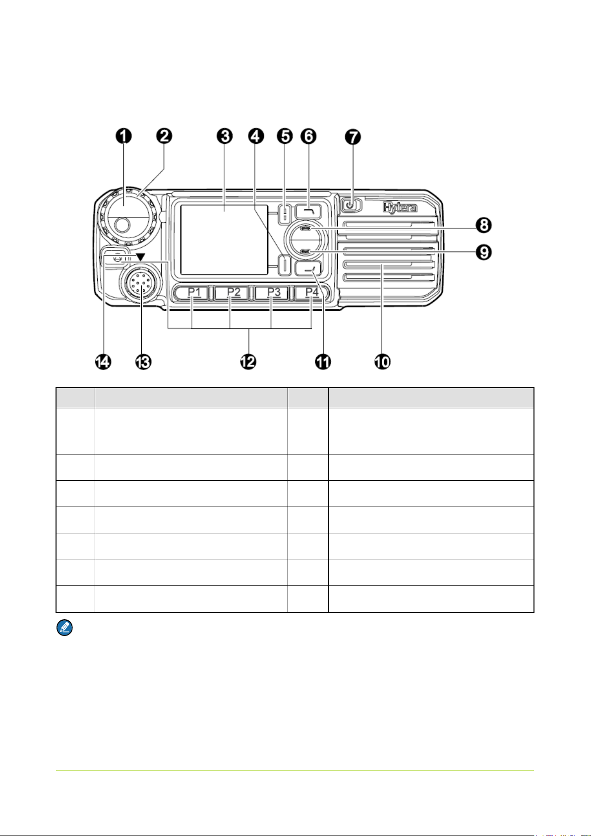
1. Product Controls
Volume Control/Group Call Selector
Front Panel
UHF1 (400–470 MHz)
No. Part Name No. Part Name
1
Knob
2 LED Indicator 9 Down Key
3 LCD Display 10 Speaker
4 OK/Menu Key 11 Redial/Answer/Call Key
5 Back/Group Call Manage me nt Key 12 Programmable Keys
6 Dial-back/End/Home Screen Key 13 Microphone Connector
7 Power On/Off Key 14 Microphone Installation I ndex
8 Up Key
Note
The above-mentioned pr oduct control is based on the mobile radio in the trunking mode. In the
conventional mode, No. 1 ser ves as Volume Control / Channel Selector Knob, and No. 6 & No.11
serve as the Programmab le K eys.
UHF1 (400–470 MHz)
2
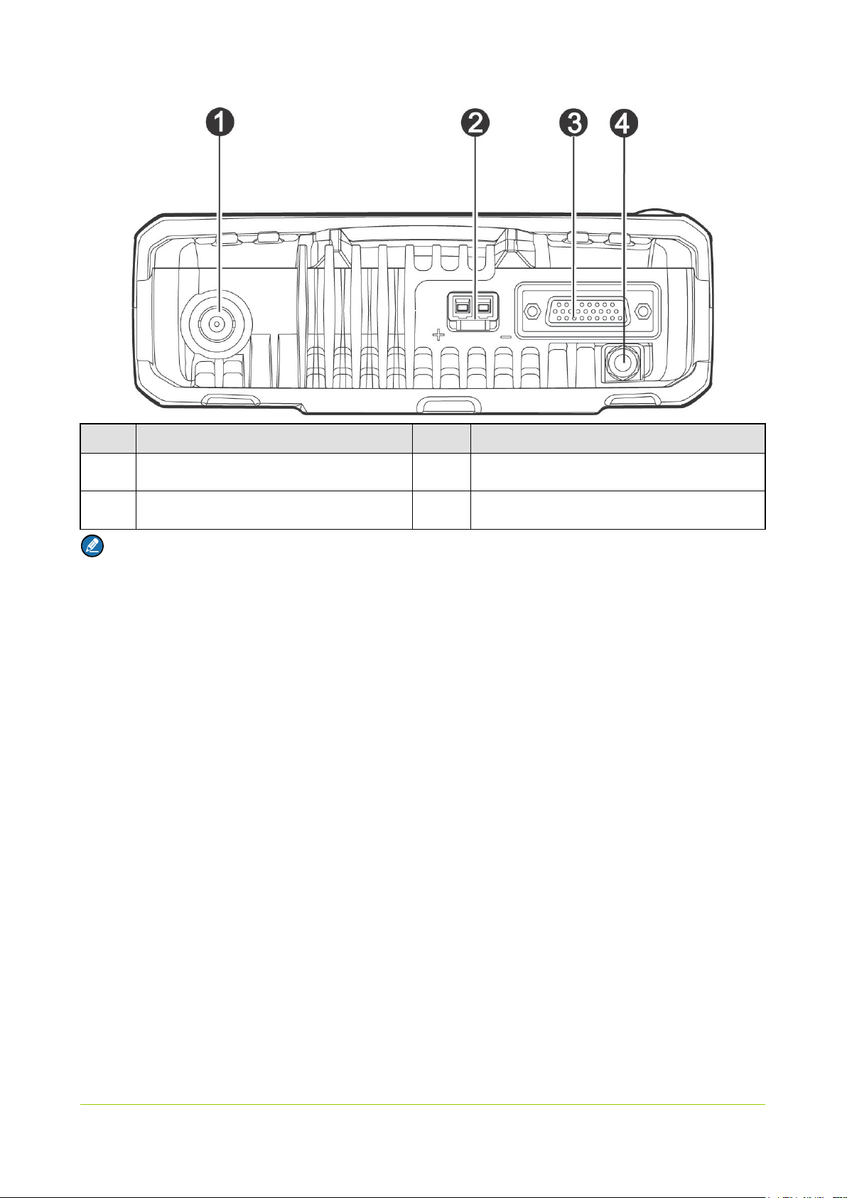
Rear Panel
No. Part Name No. Part Name
1 RF Antenna Connector 3 Accessory Connector
2 Power Inlet 4 GPS Antenna Connector
Note
The GPS antenna interfac e is only available for MD78XG.
UHF1 (400–470 MHz)
80
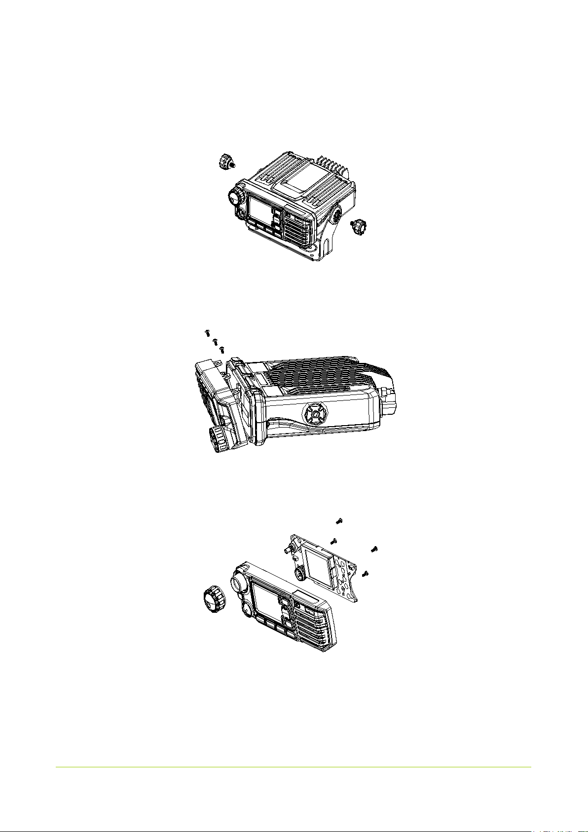
2. Disassembly and Reassembly
2.1 Disassembling the Radio
Step 1 Turn off the radio and remov e t he power cord, and loosen the two screws to remov e t he r adio.
Step 2 Remove the antenna.
Step 3 Loosen the three screws to r em ove the front panel. Then remove the FFC.
Step 4 Detach the volume control knob and loosen the four screws. Then remove the PC B from the
control panel.
Step 5 Undo the clips on both sides of the radio, and then remove the rear cover.

4
Step 6 Loosen the eleven screws t o r emov e t he upper shield cover.
UHF1 (400–470 MHz)
Step 7 Loosen the screw fixing th e ant enna co nne ctor and t wo scr ews f ixing th e P A modu le. Th en ta ke
the PCB out.
2.2 Reassembling the Radio
To reassemble the radio, per f orm the above steps in a reverse way.

UHF1 (400–470 MHz)
80
1
6300109000000
Aluminum chassis
1
27
6100334000000
O-ring for encoder switch
1
2
7500358000000
Heat sink pad
1 28
4399030000020
Rotary switch
1
3
6100492101000
Waterproof ring for front
case
1 29
41078001000J0
PCB for control panel
1
4
4210090000200
Signal cable
1 30
6100533101000
Waterproof ring for
aluminum chassis
1
5
5208010100010
Connector (male)
1 31
6300126000000
Upper cover of the
aluminum chassis
1
6
6001079000000
Light-guide plate for keys
1 32
7103015000000
Machine screw
11
7
7300048000000
Metal dome
1 33
6001080000000
Plastic upper cover
1
8
6100408001000
Waterproof ring for
microphone jack
1 34
6100496000000
Conductive silicone
rubber for main board
1
9
6100488000000
P+R front panel keys
1 35
7103008000400
Machine screw
2
10
6201893000000
Speaker fixing sheet
1 36
7500272000000
Heat sink pad
2
11
7102606021000
Self-tapping screw
6 37
/
Semi-finished PA with
heat sink pad
1
3. Exploded View and Packing Guide
3.1 Exploded View
Part list:
No. Part No. Description Qty. No. Part No. Description Qty.
UHF1 (400–470 MHz)
6
12
4210080000700
Speaker cable (with 2-Pin
plug)
1 38
3414999000020
PNP transistor
1
13
5001210000390
Speaker
1 39
/
Main PCB
1
14
7400297000000
Speaker felt
1 40
6100532100000
D_SUB waterproof ring
1
15
7102505000110
Machine screw
3 41
5208026100000
Jack
1
16
6001076000010
Front case for control
panel
1 42
6100530100000
Waterproof ring for power
socket
1
17
860P580600100
Logo
1 43
5205002100110
Power socket (male)
1
18
6201739000000
Inner lining for knob
1 44
3103994770150
Electrolytic capacitor
1
19
6000876000000
Encoder knob
1 45
7212002500000
Nut
1
20
6100493000000
Power on/off key
1 46
6100531100000
Waterproof ring for
antenna connector
1
21
6100404000000
Emergency key
1 47
4401000009000
BNC RF connector
1
22
7500344000000
PORON pad
1 48
6100494000000
GPS soft stopple
1
23
5130000000040
TFT LCD 2. 0" TFT
1 49
7500159000100
Thermal conductive
silicone rubber
2
24
6001078000000
LCD bracket
1 50
7500357000000
Heat sink pad
1
25
5202002100270
Board-to-wire connector
1 A
6100574100000
O_ring
11
26
7207003700000
Nut
1 B
7500344000000
PORON pad
1
No. Part No. Description Qty. No. Part No. Description Qty.
Note
Parts that are not mar ked with Part No. may vary with the radio frequency band.
80
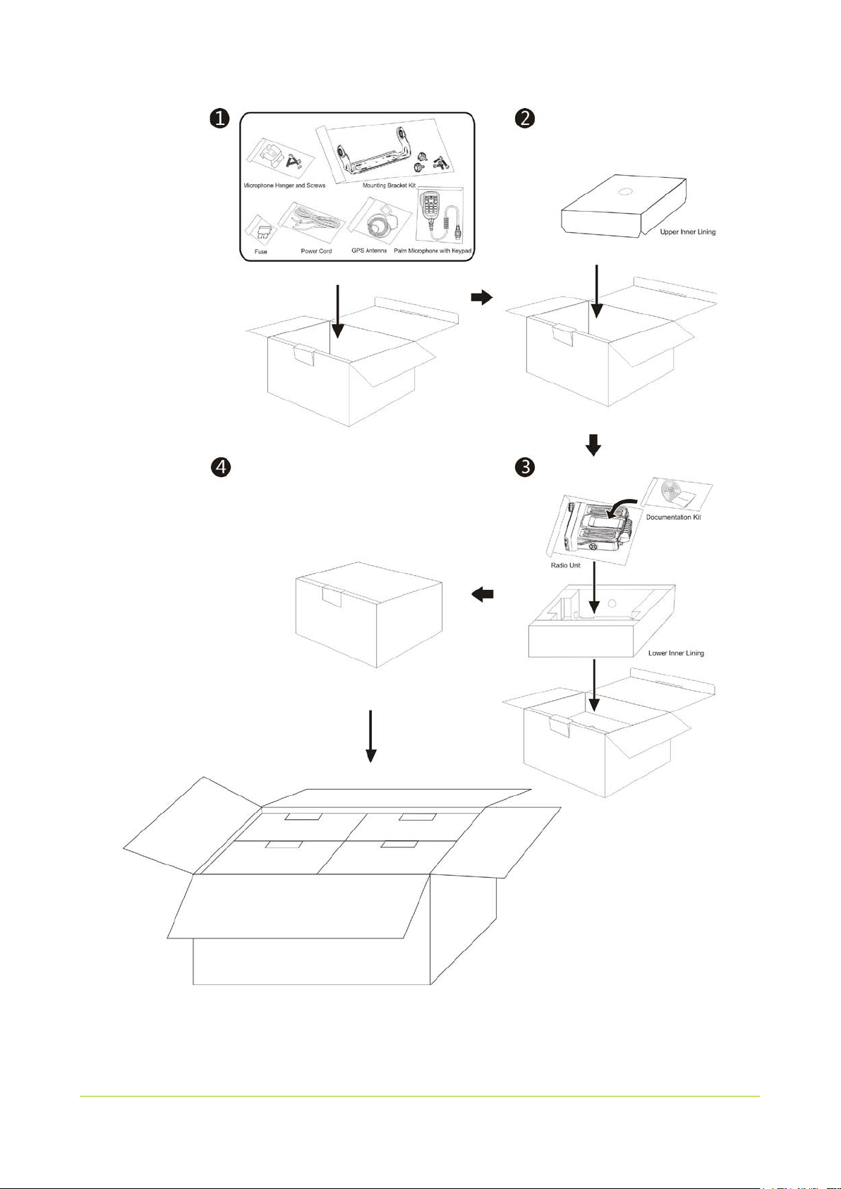
3.2 Packing Guide
UHF1 (400–470 MHz)
8
4. Specifications and Blind Spot
4.1 Specifications
General
UHF1 (400–470 MHz)
Frequency Range
Channel Capacity 1024
Group Capacity 64 (each with a maximum of 16 c hannels)
Channel Spacing 12.5 kHz / 25 kHz
Operating Voltage 13.6V±15% DC
Current Drain
Frequency Stability ±2.5 ppm
Antenna Impedance 50 Ω
Dimension s ( H×W×D) 60 mm × 174 mm × 200 mm (2.4 inch × 6.9 inch × 7.9 inch)
400–470 MHz
Standby: <0. 6 A
Receive: <2.0 A
Transmit: 5 W: <5 A; 25 W: <8 A, 45 W: <12 A
Weight 1.7 kg (3.75 lbs)
LCD Display 220*176 pixels, 262000 colors, 2. 0-inch, 4 rows
Transmitter
Low: 1–25 W
Power Output
High: 1–45 W
Conducted/Radiated
Emission
FM Modulation
4FSK Digital Modulation 12.5 kHz (data only): 7K70FXD
Modulation Limit
-36 dBm <1 GHz
-30 dBm >1 GHz
10K1F3E@12.5 kHz
15K1F3E@25 kHz
±2.5 kHz@12.5 kHz
±5.0 kHz@25 kHz
80
FM Hum and Noise
Spurious Response
Adjacent Channel Power
UHF1 (400–470 MHz)
40 dB@12.5 kHz
45 dB@25 kHz
60 dB@12.5 kHz
70 dB@25 kHz
Audio Response
Audio Distortion
Digital Vocoder Type
Digital Protocol
Sensitivity
Adjacent Channel
+1 dB to -3 dB
≤3%
AMBE++ or SELP
ETSI-TS102 361-1, -2, -3
Receiver
Analog:
0.3 μV (12 dB SIN AD)
0.22 μV (Typical) (12 dB SINAD)
0.4 μV (20 dB SIN AD)
Digital:
0.3 μV /BER5%
TIA-603: 65 dB@12.5 kHz/75 dB@25 kHz
Selectivity
Intermodulation
Rejection
Blocking
Hum and Noise
Rated Audio Power
Max. Audio Power Internal (20 Ω load): 8 W
ETSI: 60 dB@12.5 kHz/75 dB@25 kHz
TIA-603: 75 dB@12.5/25 kHz
ETSI: 70 dB@12.5/25 kHz
TIA-603: 75 dB@12.5/25 kHz
ETSI: 70 dB@12.5/25 kHz
TIA-603: 90 dB
ETSI: 84 dB
40 dB@12.5 kHz
45 dB@25 kHz
Internal (20 Ω load): 3 W
External (8 Ω load): 7.5 W

10
External (8 Ω load): 20 W
Rated Audio Distortion ≤ 3%
Audio Response +1 dB to -3 dB
UHF1 (400–470 MHz)
Conducted Spurious
Emission
Operating Temperature -30℃ to +60℃
Storage Temperature -40℃ to +85℃
ESD
American Military Standard MIL-STD-810 C/D/E/F/G
Dust & Water Protection IP54
< -57 dBm
Environment
IEC 61000-4-2 (level4)
±8 kV (contact)
±15 kV (air)
Humidity Per MIL-STD-810 C/D/E/F/G Standards
Shock and Vibration Per MIL-STD-810 C/D/E/F/G Standards
GPS (for MD780XG only)
Accuracy specs are for lo ng-term tracking (95th percentile values>5 satellites visible at a nominal
-130dBm signal strength).
TTFF (Time To Fir s t Fix)
Cold Start
TTFF (Time To Fir s t Fix)
Hot Start
Horizontal Accuracy <10 m
< 60s
<10s
Note
All Spec if ic ations are tested according to applicable standards, and subject to change without not ice
due to continuous develop me nt .

UHF1 (400–470 MHz)
80
4.2 Blind Spot
No. Blind Spot (MHz) No. Blind Spot (MHz)
1 403.2 5 414
2 422.4 6 432
3 441.6 7 450
4 460.8 8 468

UHF1 (400–470 MHz)
12
Pin 1 and Pin 10 (accessory
2) compose
an accessory identification
matrix. Please refer to the
pin Accessory Identification
PTT input for the palm
microphone, which is valid at
External audio
60% system max.
Accessory audio output. When
“Mic Audio Output” is selected
via CPS, this pin will output the
USB data
USB power
This pin provides power supply
a 5 V voltage when accessory
identification code is 00|01|10,
puts low level when the
5. Interface Definition
5.1 10-Pin Connector
The 10-pin connector on the front panel is used for audio accessories or dat a cable connection. The
definition of each pin is descr ib ed as below.
Pin
No.
1
2 PTT input Digital inpu t 3.3 V CMOS
3
Name Type
Accessory
identification
interface 1
output
Digital inpu t 3.3 V CMOS
Analog
output
Signal Electrical
Performance
Load impedance >1 kΩ
Vrms=600mV±10%@1
kHz
Description
identifier interface
“10-
Matrix Table” below for detailed
function definitions.
low level.
4 USB_D-
5 GND
6 USB_VBUS
cable-
Ground
cable
supply
deviation
USB data
/ /
Power supply: 5 V; current
limiting: 500 mA
received audio signal.
When this pin is used for USB
function, USB function of DB26
will be disabled.
to the USB accessory. It outputs
and out
code is 11.

UHF1 (400–470 MHz)
80
USB data
Press this key, the level
palm microphone is detected or
press the key of the palm
HOOK function; when desktop
microphone is detected, this pin
Pin 1 and Pin 10 (accessory
identifier interface 1) compose
Please refer to the
pin Accessory Identification
The mobile radio is in USB master mode or connected to a USB
Pin
No.
7 Mic input Analog input
8 USB_D+
9 HOOK Digital inpu t 3.3V CMOS
Name Type
cable+
Signal Electrical
Performance
Modulation sensitivity
Vrms=80mV±10%@1kHz
60%system max. deviation
USB data
Description
Mic input for palm microp hone
When this pin is used for USB
function, USB function of DB26
will be disabled.
High level by default ; v alid at low
level.
HOOK and MONITOR functions:
changes from high to low. When
microphone, this pin is used for
is used for MONITOR func t ion.
Accessory
identification
10
interface 2
10-pin Accessory Ident ification Matrix Table (composed of Pin 1 and Pin 10):
Pin 1 Pin 10 Radio Status
Low level Low level Reserved
Digital inpu t 3.3V CMOS
an accessory identification
matrix.
“10-
Matrix Table” below for detailed
function definitions.
Low level High level
High level Low level
smart accessory (such as palm microphone with keypad).
The mobile radio is connected to an external speaker (including
desktop microphone with earpiece).
UHF1 (400–470 MHz)
14
Pin 1 and Pin 10 (accessory
identification interface 2)
compose an accessory
matrix. This pin
outputs a 5 V voltage when
accessory identification code is
00|01|10, and outputs low level
Power output: 13.2 V; output
Pin 1 Pin 10 Radio Status
The mobile radio is in USB slave mode, or it is not connected to any
High level High level
accessory, or it is connected t o a palm microphone without keypad.
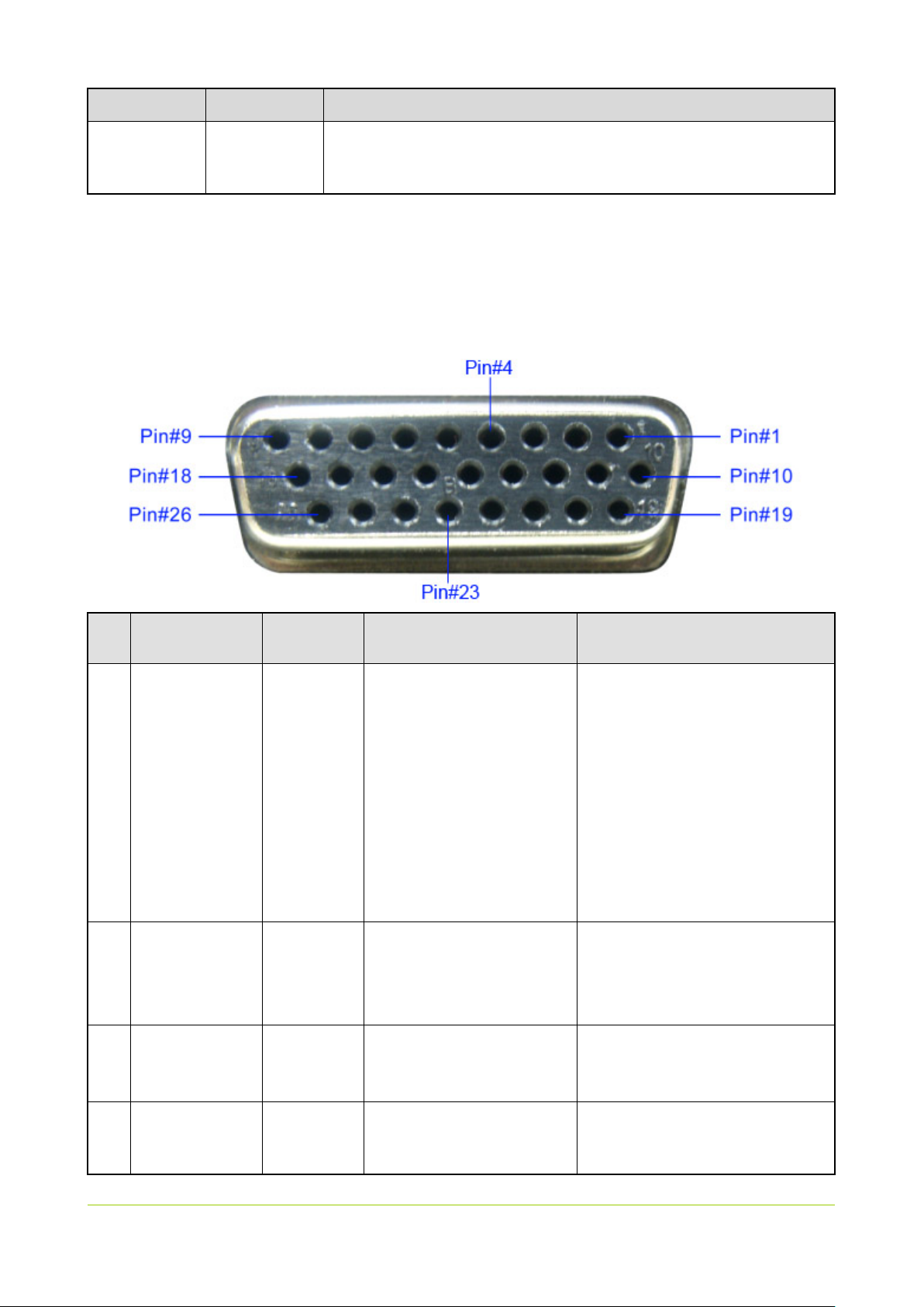
5.2 DB26 Accessory Interface
DB26 accessory interface, namely the 26-pin further development i nterface on the rear panel, is mainly
used for accessory connection of mobile radio, or compatibility with other interfaces. Users can further
develop the radio via this inter face. The figure and definition of each pin is as follows.
Pin
No.
Vbus USB
1
power supply
2 Ground
Name Type
Power
output
Power
supply
(grounding)
Signal Electrical
Performance
Power supply: +5V; current
limiting: 500 mA
/ /
Description
identification
when the code is 11.
GP5_3
3
(Chan_Act)
4 SWB+
GPIO 5V TTL GPIO. Programmable via CPS.
Power
output
Power supply :13.2V±15%;
output current ≤1 A
current: ≤1 A

UHF1 (400–470 MHz)
80
Programmable output pin
(“External Horn & Lights” feature
by default, programmable via
60% system max.
external MIC. The audio path is
valid when the external Mic PTT
60% system max.
Default output is 300 mV. The
output signal amplitude can be
changed by modifying the
It forms differential output
together with SPK+. Max
: 10 W(R=8
USB data
GPIO. Programmable via CPS;
Pin 15 (ACC_IO3) can compose
ccessory identification
Please refer to the
DB26 Accessory Identification
Pin
No.
Name Type
5 External Alarm
6 Power Ground
7 TX Audio
8 RX Audio
Analog
voltage
output
Power
supply
(grounding)
Analog
signal input
Analog
signal
output
Signal Electrical
Performance
13 V alarm output
/ /
Vrms=80 mV±10%@1 kHz
deviation
Load impedance>1kΩ
Vrms=300 mV±10%@1
kHz
deviation
Description
CPS).
This pin is used for signal input of
is held down.
“Analog RX Gain” value v ia CPS.
Analog
9 SPK-
output
power output
Ω)
10 D+
USB data USB data cable+
cable+
Ground
11 USB_GROUND
/ /
cable
GP5_2
12
GPIO 5V TTL
(Monitor)
13 ACC_IO2 Digital inpu t 5V TTL
External speaker output-
Monitor feature by default.
Accessory identification in terface;
high level by default. This pin and
three a
statuses.
“

UHF1 (400–470 MHz)
16
below for detailed
Emergency switch. This pin is
Pin 13 (ACC_IO2) can compose
ccessory identification
statuses. Please refer to the
DB26 Accessory Identification
function is programmable via
It forms differential output
. Max
power output: 10 W(R=8
USB data
Pin
No.
14 Emerg Sw Digital inpu t 5V TTL
15 ACC_IO3 Digital inpu t 5V TTL
Name Type
Signal Electrical
Performance
Description
Matrix Table”
function definitions.
valid when low level is input.
Accessory identification in terface;
high level by default. This pin and
three a
“
Matrix Table”” below for detailed
function definitions.
16 PRGM_IN_PTT Digital input 5V TTL
Audio
17 Audio Ground
18 SPK+
19 D-
20 GP5_8
(grounding)
Analog
signal
output
cable-
Digital
input/output
/ /
together with SPK-
Ω)
USB data USB data cable-
5V TTL GPIO. Programmable via CPS.
Programmable input pin (PTT
key of external Mic by default; its
CPS). It is valid at low level.
External speaker output+
21 Ground
22 GP5_7
Ground
/ /
cable
Digital
5V TTL GPIO. Programmable via CPS.
input/output

UHF1 (400–470 MHz)
80
radio is in USB slave mode or not
The mobile radio is in USB master mode or connected to a USB
an external speaker (including
Pin
No.
23 GP5_6
24
25
26
Note
When a pin is marked with 5 V TTL level, this pin has the pull-up funct ion. If the pin needs t o be set to
Name Type
Digital
input/output
AUX Audio Out 1 Analog
output
AUX Audio Out 2 Analog
output
Analog
Ign Sense
voltage
Detect Pin
input
Signal Electrical
Performance
5V TTL GPIO. Programmable via CPS.
Load impedance >1 kΩ
Vrms=300 mV±10%
Load impedance >1 kΩ
Vrms=300 mV±10%
Ignition voltage input >7 V Input pin for ignition voltage
Auxiliary audio (external s peaker )
output 1
Auxiliary audio (external s peaker )
output 2
Description
high level, empty this pin.
DB26 Accessory Identification Matrix Table (composed of Pin 13 and P in 15):
Pin 13 Pin 15 Radio Status
High level High level
High level Low level
Low level High level
Low level Low level Reserved
Default status. The mobile
connected to any accesso r y.
smart accessory (such as palm microphone with keypad).
The mobile radio is connected to
desktop microphone with earpiece).
5.3 Other Interfaces
J2 (LCD Display Interface)
Pin No. Name Description
1 GND Grounding pin
2 VCI 2.5–3.3 V adjustable port
3 VCI 2.5–3.3 V adjustable port
4 IOVCC 1.65–3.3 V adjustable I/O port

18
Pin No. Name Description
5 FLM Synchronization signal c ontrol port
6 CS Chip select signal
7 RS Register select
8 WR Write signal
9 RD Read signal
10 DB0
11 DB1
12 DB2
13 DB3
UHF1 (400–470 MHz)
14 DB4
15 DB5
16 DB6
17 DB7
18 DB8
19 DB9
20 DB10
21 DB11
22 DB12
23 DB13
24 DB14
Data bus
25 DB15
26 DB16
27 DB17
28 RESET Reset signal
29 IM3 Select data cable

80
Pin No. Name Description
setting the option
Unidirectional output
interfaces. They require
their input resistances
are greater than or
30 IM0
31 LEDA LED anode
32 LED_K1
UHF1 (400–470 MHz)
33 LED_K2
34 LED_K3
LED cathode
J4 (Aviation Interface of Front Panel)
Pin No. Name Description
1 ACC_IO1 Digital input
2 PTT_IN Digital input
3 External_Audio Analog output
4 USB_D- USB data cable
5 GND Ground cable
6 USB_VBUS Power supply
7 MIC_IN Analog input
8 USB_D+ USB data cable
9 HOOK Hook signa l input
10 ACC_IO2 Digital input
J400 (Option Board Interface)
Pin No. Signal Function
1 GPIO1
3 GPIO2
5 GPIO3
7 GPIO4 O
9 GPIO5 RESET-OUT O
GPIO
I/O of the
Radio
I/O
Voltage
(Option Board
VDD=3.3 V)
VIH MIN=0.7VDD
VIL MAX=0. 3VDD
VOH MIN=0. 8VDD
VOL MAX=0.22VDD
Remark
GPIO5: output signal of
re
board.
GPIO4/GPIO5:
UHF1 (400–470 MHz)
20
AF OB TO
80 mV (standard
output from the
to the
AF MB TO
80 mV (standard
board to the option
Pin No. Signal Function
11 UART-TX
13 UART-RX I
UART-CT
15
S
UART-RT
17
S
2 I2C –SDA
4 I2C -SCL O
MCBSP-D
6
R
UART
I2C
I/O of the
O
I
O
I/O
I
Radio
Voltage
(Option Board
VDD=3.3 V)
Remark
equal to 47 kΩ.
UART
I2C
MCBSP-W
8
10
12
14 AGND AGND / / /
16
18
CLK
MCBSP
MCBSP-D
X
MCBSP-F
SX
AF I
MB
AF O
OB
I/O
O
I/O
option board
main board)
output from the main
McBSP: Multi-channel
buffered serial port
MAX: 700 mV
MAX: 700mV
19 DGND DGND / / /
20 3V6 or 5V Power O Voltage: 5.0 V /
board)

80
J403 (Pin Interface)
Pin No. Name Description
1 Vbus USB Power supply: +5 V
2 Ground Ground cable
UHF1 (400–470 MHz)
3
4 SW B+ sense Power supply
5 External Alarm Ana lo g voltage output
6 Power Ground Power supply (grounding)
7 Tx Audio Analog input
8 RX Audio Analog output
9 Spkr- Analog output
10 D+ USB USB data cable+
11 USB_GROUDN Ground cable
12
13 ACC_IO2 Digital input
GP5_3
GP5_2
Digital input/output
Digital input/output
14 Emerg Sw Digital input
15 ACC_IO3 Digital input
16 PRGM_IN_PTT Digital input
17 Audio Ground Audio ground
18 Spkr+ Analog output
19 D- USB USB data cable-
20
21 Ground Ground cable
22
23 GP5_6 Digital input/output
24 AUX Audio Out 1 Analog output
GP5_8
GP5_7
Input/output
Input/output

22
Pin No. Name Description
25 AUX Audio Out 2 Analog output
26 Ign Sense Ana lo g voltage input
J404 (Front Panel Interface)
Pin No. Name Description
1 INT_MIC Audio input
2 MIC_GROUND Audio input (grounding)
3 ACC_IO1 Accessory identificatio n interface 1
4 USB_VBUS USB power supply
5 HOOK HOOK
UHF1 (400–470 MHz)
6 PTT PTT
7 USB_D- USB data cable D-
8 USB_D+ USB data cable D+
9 ACC_IO2 Accessory identificatio n interface 2
10 UART2_RXD_A Volume c ont r ol port
11 UART2_TXD_B /
12 EXTERNAL_AUDIO Audio signal out put by accessory (mobile radio)
13 SPKR1+ Speaker audio signal cable+
14 SPKR1- Speaker audio signal cable-
15 5VD Power supply
16 PRST Reset signal
17 KB_C0
18 KB_C1
19 KB_C2
20 KB_C3
21 B_R0
Matrix keyboard
80
Pin No. Name Description
22 B_R1
23 B_R2
24 CSLED Backlight control IC chip select
25 CLOC Backlight control IC clock
26 DATA Backlight control IC data
27 OE_LCD LCD read enable
28 WE_LCD LCD write enable
29 CS2_LCD LCD chip select
30 F_A1_LCD LCD register se lect enable
UHF1 (400–470 MHz)
31 F_D7
32 F_D6
33 F_D5
LCD data bus
34 F_D4
35 F_D3
36 F_D2
37 F_D1
LCD data bus
38 F_D0
39 GND Grounding
40 PWB_IN Power On/Off signal

24
6. Tuning Description
Reference Oscillator
Connect the radio to HP8 921 v ia the ante nna c onn ector, and set H P8921
Adjust the vernier on the Tuner until the frequency offset between the
frequency displayed on HP8921 and the frequency (Tx) displayed on
Transmit Power
Connect the radio to HP8 921 v ia the ante nna c onn ector, and set H P8921
> Transmit
Power Calibration” in the left navigation tree. Then select an appropriate
6.1 Required Test Instruments
Radio communic at io n test sets: HP8921 and A er oflex 3920
Power supply: 15 A/30 V
Multimeter
Tuner software
6.2 Tuning Procedures
UHF1 (400–470 MHz)
6.2.1
After re-assembling the radio, you nee d t o t une it with the Tuner software and HP8921.
The specific operations are described in the table below. After tuning the ite m s of the c ur rent channel,
you must switch the radio to t he next c hannel; otherwise, the adjustments will not be sav ed t o t he r adi o
properly.
TX Section
Warp
Tuning the Radio
Items Method
1.
to TX test mode.
2. Open the Tuner software and go to “TUNE_DATA -> TX -> Reference
Oscillator Warp” in the left navigation tree. Then click the “Transmit On”
button.
3.
Tuner is less than or equals to ±40 Hz.
4. Click the “Save” butt on on Tuner to save the existing value to the radio.
5. Click the “Transmit Off” button on Tuner.
Calibration
Here takes the tuning of low TX power for example.
1.
to TX test mode.
2. Open the Tuner software and go to “TUNE_DATA -> TX -
channel.

80
Items Method
Connect the radio to HP8 921 v ia the ante nna c onn ector, and set H P8921
Adjust the vernier on Tuner until the frequency deviation displayed on
Connect the radio to HP8 921 v ia the ante nna c onn ector, and set H P8921
Click the “Transmit On” button on Tuner. Then set the modulation signal
3. Click the “Transmit On” bu t ton on Tuner.
Adjust the power to the required level as follows:
4.
Low power: 1 W (for version D/F)
Medium power: 25 W
High power: 45 W
5. Click the “Save” button on Tuner t o save the existing value to the radio.
1.
to TX test mode.
2. Set the parameters on the HP8921 as fol low s:
IF Filter: 230 kHz
Filter1: <20 Hz HPF
UHF1 (400–470 MHz)
Filter2: <15 kHz LPF
Transmit-to-Deviation
De-Emphasis: off
3. Open the Tuner software and go to “TUNE_DATA -> TX T
ransmit-to-Deviation” in the left nav ig at ion tree. Then click the “Transmit
On” button. Then set the modulation signal of HP8921 to “100 Hz”.
4.
HP8921 is “5 kHz”.
5. Click the “Save” button on Tuner t o save the existing value to the radio.
6. Click the “Transmit Off” bu tton on Tuner.
Here takes the low freque ncy deviation for example.
1.
to TX test mode.
2. Set the parameters on the HP8 921 as follows:
>
Modulation Balance
IF Filter: 230 kHz
Filter1: <20 Hz HPF
Filter2: <15 kHz LPF
De-Emphasis: off
3. O
pen the Tuner software and go to “TUNE_DATA -> TX -> Modulation
Balance” in the left navigation tree. Then select an appropriate chann el.
4.

26
Transmit Oscillator
Voltage
Connect the radio to HP8 921 v ia the ante nna c onn ector, and set H P8921
> Transmit
Filter” in the left navigation tree. Adjust the vernier on Tuner until the
UHF1 (400–470 MHz)
Items Method
of HP8921 to “100 Hz”.
5. Adjust the value in the dialog box on Tuner until the frequency deviation
displayed on HP8921 is “5 kHz ” .
6. Press the Enter key on the keyboard to confirm your settings.
7. Click the “Save” butt on on Tuner to save the existing value to the radio.
8. Click the “Transmit Off” button on Tuner.
1.
to TX test mode.
2. Open the Tuner software and go to “TUNE_DATA -> TX Oscillator Voltage” in the l eft navigation tree.
3. Click the “Save” butt on to save the existing value to the radio.
RX Section
Front-end Filter
1. Connect the radio to H P8 921 via the antenna connector.
2. Connect the Audio Out port of the radio to the Audio In port of HP8921,
and set HP8921 to RX test mode.
3. Set the parameters on t he HP8921 as follows:
Output RF signal: -118 dBm/Frequency (current channel frequency )
Modulation frequency: 1 k Hz
Modulation deviation: 3 kHz
4. Open the Tuner software and go to “TUNE_DATA -> RX -> Front-end
“SINAD” value displayed on H P8921 is greater than 14 dB.
5. Set the output RF signa l of HP8921 to -25 Bm/(current channel frequency
-36.675 MHz).
6. Adjust the vernier o n Tuner until the “SINAD” value displayed o n H P8921
is less than 14 dB.
7. Press the Enter key on the keyboard to confirm your settings.
8. Click the “Save” butt on on Tuner to save the existing value to the radio.
1. Connect the radio to HP8921 via the antenna c onn ector , and set HP8 921
Front-end Gain
to RX test mode.
2. Set HP8921 to output an unmodulated RF signal with a value of “-70

80
Items Method
Receive Oscillator
Connect the radio to HP8 921 v ia the ante nna c onn ector, and set H P8921
dBm/Frequency (current channel frequency)”.
3. Press the Enter key on the keyboard to confirm your settings.
4. Click the “Save” butt on on Tuner to save the existing value to the radio.
1.
to RX test mode.
2. Open the Tuner software and go to “TUNE_DATA -> RX -> Receive
Oscillator Voltage” in the l eft navigation tree.
Voltage
3. Set HP8921 to output an unmodulated RF signal with a value of “-47
dBm/Frequency (current c hannel frequency)”.
4. Click the “Save” butt on to save the existing value to the radio.
6.2.2 Testing the Radi o
UHF1 (400–470 MHz)
After tuning all the items of the radio, you need to test the digital RF signal of the mobile radio via
Aeroflex 3920 (Digital Ra dio Test set).
Transmitting
Step 1 Connect the mobile radio to Aeroflex 3920 via the antenna connector.
Step 2 Open the T uner software and go to “TEST -> TX -> Transmit B ER (0.153)”.
Step 3 Select the channel to be tested and select the corr esponding power level (High Power or Low
Power) in “Parameter” on Tuner.
Step 4 Click the “Transmit On” bu t ton on Tuner.
Step 5 Set the parameters on the Aeroflex 3920 as follows:
Frq: Be consistent with the TX frequency of the c hannel to be tested.
STD IB 511: .153
Step 6 Observe the “avg” v alue of “UUT TX Bit Err” parameter in “UUT Measurement s ” mo dul e of
Aeroflex 3920, which is th e average bit error rate of the tested channel during t r ansmitting.
The radio is operating pro per ly when the Aeroflex 3920 parameters are a s fo ll ow s:
FSK Error: ≤5%
Symbol Clock Err: ≤100 Hz
Signal Power: 3. 9–4.5W
Magnitude Error: ≤1%
UUT TX Bit Err = 0%

UHF1 (400–470 MHz)
28
Step 7 Click the “Transmit Off” bu tton on Tuner to finish testing.
Receiving
Step 1 Connect the antenna connec t or of the radio to the RF port of Aeroflex 3920, and set A er oflex
3920 as follows (remain default values for other parameters):
Frq: Be consistent with the frequency of the channe l t o be t ested.
STD IB 511: .153
Lv1 (signal strength): -116 dBm (-11 0 dBm by default)
Step 2 Open the T uner software and go to “TEST -> RX -> Receiver BER (0.153)”.
Step 3 Select the channel to be tested and click the “Start” button on Tuner.
Step 4 Observe the “Average Rate” displayed on Tuner.
You can set different “Aver age Num” (the calculation base of BER, which is “10” by default) to
obtain different “Average Rat e” .
Step 5 Modify the value of “Lv1” par ameter of Aeroflex 3920, so as to obtain the average BERs of the
tested channel under different signal strengths.
The mobile radio is oper at ing properly when the average BER is less than 5% .
Note
When the parameter “ Lv1” is set to “-110 dBm”, the mobile radio is operating properly when
the average BER is less than 1% .
Step 6 Click the “Stop” button on Tun er t o finish testing.


UHF1 (400–470 MHz)
81
This equipment has been tested and found to comply with the limits for a Class B digital device, pursuant to Part
15 of the FCC Rules. These limits are designed to provide reasonable protection against harmful interference in a
residential installation. This equipment generates, uses and can radiate radio frequency energy and, if not
installed and used in accordance with the instructions, may cause harmful interference to radio communications.
However, there is no guarantee that interference will not occur in a particular installation.
If this equipment does cause harmful interference to radio or television reception, which can be determined by
turning the equipment off and on, the user is encouraged to try to correct the interference by one or more of the
following measures:
-- Reorient or relocate the receiving antenna.
-- Increase the separation between the equipment and receiver.
-- Connect the equipment into an outlet on a circuit different from that to which the receiver is connected.
-- Consult the dealer or an experienced radio/TV technician for help.
This equipment complies with FCC radiation exposure limits set forth for an controlled environment. This
equipment should be installed and operated with minimum distance 100cm between the radiator and your body.
This transmitter must not be co-located or operating in conjunction with any other antenna or transmitter.
This equipment complies with IC RSS-102 radiation exposure limits set forth for an controlled environment. This
equipment should be installed and operated with minimum distance 100cm between the radiator and your body.
Cet équipement est conforme aux limites d'exposition aux radiations IC CNR-102 établies pour un
environnement contrôlé. Cet équipement doit être installé et utilisé avec une distance minimale de 440 cm entre
le radiateur et votre corps.
This device contains licence-exempt transmitter(s)/receiver(s) that comply with Innovation, Scien ce and Econ om ic
Development Canada’s licence-exempt RSS(s). Operation is subject to the following two conditions:
(1) This device may not cause inter f erence.
(2) This device must accept any interference, including interference that may cause undesired operation of the device.
L’émetteur/récepteur exempt de licence contenu dans le présent appareil est conforme aux CNR d’Innovation, Sciences
et Développement économique Canada applicables aux appareils radio exempts de licence. L’exploitation est autorisée
aux deux conditions suivantes :
(1) L’appareil ne doit pas produire de brouillage;

UHF1 (400–470 MHz)
80
(2) L’appareil doit accept er tou t broui llage rad ioélec triqu e sub i, même s i le broui llage e st sus ceptible d’en co mpromet tre le
fonctionnement.
 Loading...