

Page 1

Service Manual
Preface
This manual describes information related with product repair. To repair the product properly, please
read this manual carefully.
This manual is applicable to the following model:
RD98X (X may indicate 2, 5, 6 or 8.)
Page 2

Service Manual
Contents
1. Revision History ...................................................................................................................................1
2. Copyright Information...........................................................................................................................2
3. Disclaimer.............................................................................................................................................
4. Introduction...........................................................................................................................................4
5. Product Controls...................................................................................................................................5
Front Panel........................................................................................................................................5
Rear Pan
6. Baseband Section................................................................................................................................6
6.1 Front Panel..................................................................................................................................6
6.2 Main Board................................................................................................................................10
6.3 PCB Vi
6.4 Block Diagram...........................................................................................................................27
6.5 Schematic Diagram...................................................................................................................
6.6 Parts List...................................................................................................................................
6.7 T
e
l........................................................................................................................................5
ew..................................................................................................................................23
roubleshooting Flow Chart ......................................................................................................77
3
29
43
7. Tuning Description..............................................................................................................................78
8. Interface Definition .............................................................................................................................79
9.UHF1 (400-470MHz) Information ........................................................................................................84
9.1 TX Circuit...................................................................................................................................84
9.2 RX Circuit..................................................................................................................................86
9.3 Frequency Generation Unit (FGU) ............................................................................................88
9.4 PCB View..................................................................................................................................
9.5 Block Diagram...........................................................................................................................96
9.6 Schematic Diagram...................................................................................................................
9.7 Parts List.................................................................................................................................
roubleshooting Flow Chart ....................................................................................................13
9.8 T
10. UHF2 (450-520MHz) Information ...................................................................................................144
10.1 TX Circuit...............................................................................................................................144
90
99
108
9
Page 3

Service Manual
10.2 RX Circuit..............................................................................................................................146
10.3 Frequency Generation Unit (FGU) ........................................................................................147
10.4 PCB View..............................................................................................................................150
10.5 Block Diagram.......................................................................................................................156
10.6 Schematic Diagram...............................................................................................................159
10.7 Parts List...............................................................................................................................168
10.8 Troubleshooting Flow Chart ..................................................................................................198
11.UHF3 (350-400MHz) Information.....................................................................................................203
1 1 .1 TX Circuit...............................................................................................................................203
11.2 RX Circuit ..............................................................................................................................205
11.3 Frequency Generation Unit (FGU).........................................................................................206
11.4 PCB View ..............................................................................................................................209
11.5 Block Diagram.......................................................................................................................215
11.6 Schematic Diagram...............................................................................................................218
11.7 Parts List................................................................................................................................
.8 Troubleshooting Flow Chart...................................................................................................258
11
12.VHF (136-174MHz) Information ......................................................................................................263
12.1 TX Circuit...............................................................................................................................263
12.2 RX Circuit..............................................................................................................................265
12.3 Frequency Generation Unit (FGU) ........................................................................................266
12.4 PCB View..............................................................................................................................269
12.5 Block Diagram.......................................................................................................................275
12.6 Schematic Diagram...............................................................................................................278
12.7 Parts List...............................................................................................................................287
12.8 Troubleshooting Flow Chart ..................................................................................................317
227
13. Disassembly and Assembly............................................................................................................322
14. Exploded View................................................................................................................................
15. Packing Guide..............................................................................................................
16. Specifications.................................................................................................................................328
17. T
able of Blind Spots........................................................................................................................330
..................327
324
Page 4

Service Manual
1. Revision History
Version Date Description
R2.0 09-2010 Initial Release
R3.5 06-2011 VHF, UHF2 and UHF3 service information is included.
1
Page 5

Service Manual
2. Copyright Information
Hytera is the trademark or registered trademark of Hytera Communications Co., Ltd. (the Company) in
PRC and/or other countries or areas. The Company retains the ownership of its trademarks and product
names. All other trademarks and/or product names that may be used in this manual are properties of
their respective owners.
The product described in this manual may include the Company’s computer programs stored in memory
or other media. Laws in PRC and/or other countries or areas protect the exclusive rights of the Company
with respect to its computer programs. The purchase of this product shall not be deemed to grant, either
directly or by implication, any rights to the purchaser regarding the Company’s computer programs. Any
of the Company’s computer programs may not be copied, modified, distributed, decompiled, or
reverse-engineered in any manner without the prior written consent of the Company.
TM
The AMBE+2
rights including patent rights, copyrights and trade secrets of Digital Voice Systems, Inc. This voice
coding technology is licensed solely for use within this product. The user of this technology is explicitly
prohibited from attempting to decompile, reverse engineer, or disassemble the Object Code or in any
other way convert the Object Code into a human readable form.
U.S. Patent Nos. #6,912,495 B2, #6,199,037 B1, #5,870,405, #5,826,222, #5,754,974, #5,701,390,
#5,715,365, #5,649,050, #5,630,011, #5,581,656, #5,517,511, #5,491,772, #5,247,579, #5,226,084 and
#5,195,166.
voice coding technology embodied in this product is protected by intellectual property
2
Page 6

Service Manual
3. Disclaimer
The Company endeavors to achieve the accuracy and completeness of this manual, but no warranty of
accuracy or reliability is given. All the specifications and designs are subject to change without notice
due to continuous technology development. No part of this manual may be copied, modified, translated,
or distributed in any manner without the express written permission of us.
If you have any suggestions or would like to learn more details, please visit our website at:
http://www.hytera.com
.
3
Page 7

4. Introduction
Intended User
This manual is intended for use by qualified technicians only.
Service Manual
4
Page 8

5. Product Controls
Front Panel
No. Part Name No. Part Name
1 Accessory Jack 9 Slot 1 RX Indicator
2 Volume Control Knob / Power Indicator 10 Alarm Indicator
Service Manual
3 Repeater Mode Indicator 11 Programmable Key
4 Analog Mode Indicator 12 LCD Display
5 Slot 2 RX Indicator 13 Channel Up (CH+)
6 Slot 2 TX Indicator 14 Navigation Knob
7 Digital Mode Indicator
8 Slot 1 TX Indicator 16 Speaker
Rear Panel
No. Part Name No. Part Name
15
Channel Down (CH-)
1 TX Antenna Interface 6 Accessory Jack
2 Optional Interface 1 7 DC Power Interface
3 RX/Duplex Antenna Interface 8 Ethernet Port
4 Optional Interface 2 9 Ground Screw
5 Monitor/Tuning Interface
5
Page 9
Service Manual
6. Baseband Section
6.1 Front Panel
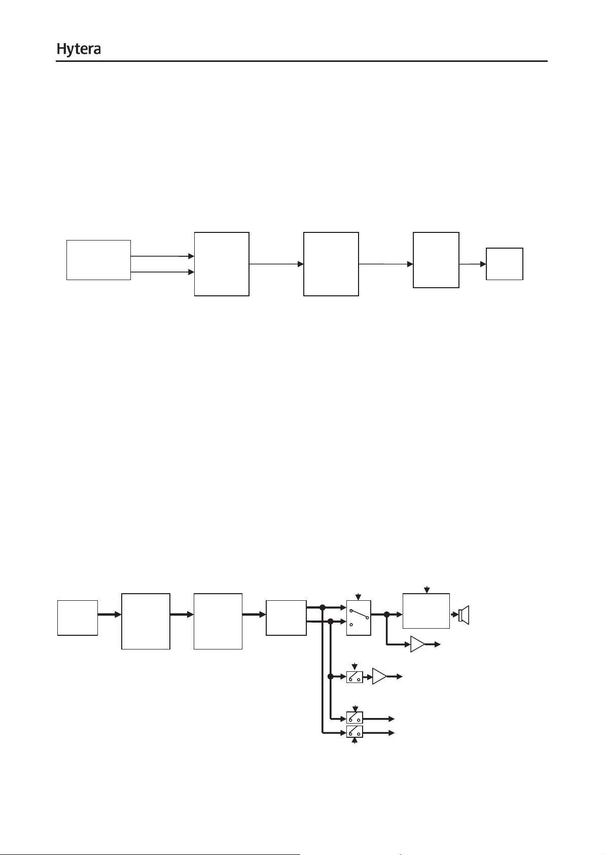
6.1.1 Overview
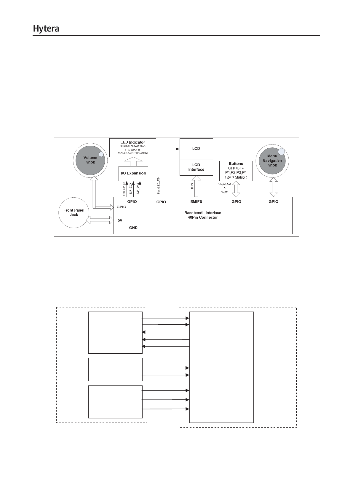
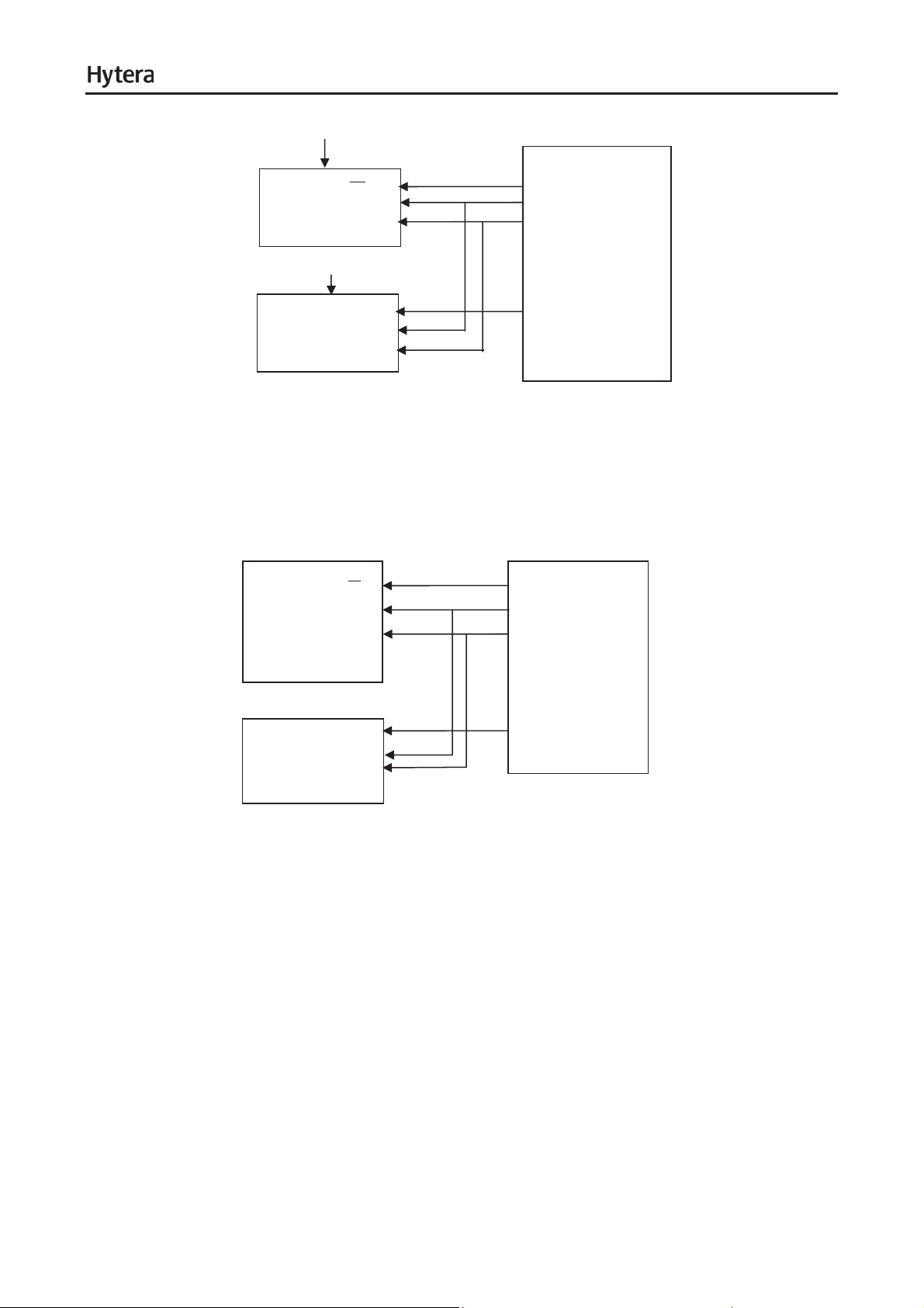
The front panel is the control panel, where you can see keys, Volume Control knob, Navigation knob,
LED indicator, LCD display and 10-Pin interface. The front panel is connected to the baseband board via
40-Pin FFC. See the following figure:
Figure 6-1 Front Panel Overview
6.1.2 Keys and Knobs
The keys on the front panel are controlled by key matrix of TX OMAP5912 (U102), and the Volume
Control knob and Navigation knob are controlled by GPIO of TX OMAP5912 (U102). See the following
figure:
KB_R0(G18)
KB_R1(F19)
KB_C0(F18)
KB_C1(D20)
KB_C2(D19)
TX OMAP5912
U102
GPIO4(P20)
GPIO6(P19)
GPIO46(W21)
GPIO49(L14)
GPIO26(AA9)
Baseband
Board
Front
Panel
BOARD
CH+/CH-
P1, P2, P3, P4
(2×3 Key matrix)
Volume control
knob
Menu navigation
knob
VOL_GPIO1
VOL_GPIO2
KNOB_A
KNOB_B
KNOB_C
Figure 6-2 Key and Knob Control Diagram for the Front Panel
6
Page 10
Service Manual
A
−
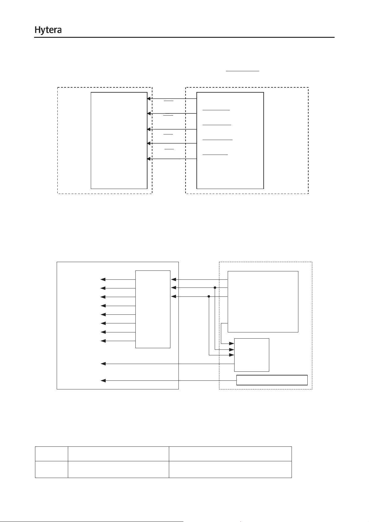
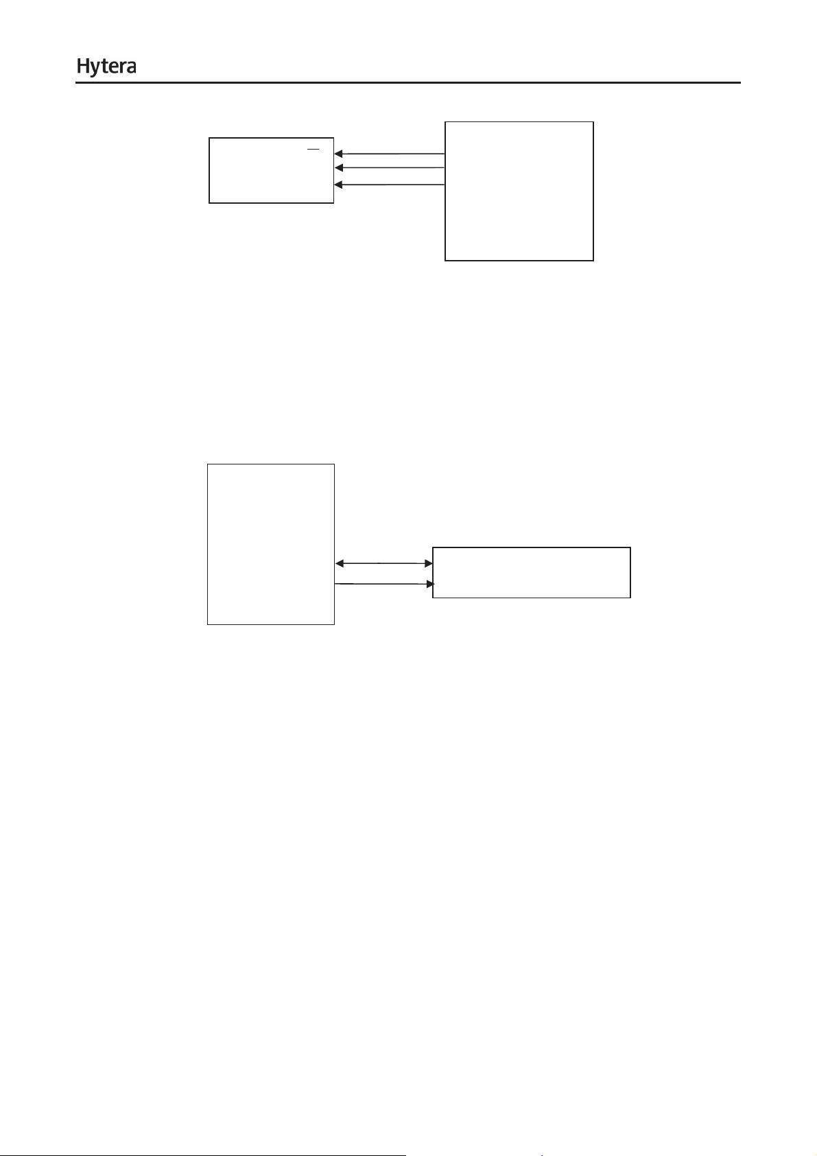
6.1.3 LCD Display
To enhance LCD refreshing rate, parallel data interface is used. It connects to EMIFS data bus of TX
OMAP5912 (U102) and the chip select is subject to the control of
D07D0
OE
FLASH.OE (U4)
WE
Front
Panel
BOARD
LCD
Interface
J1
CS
1
FLASH.WE (W2)
FLASH.CS2 (M4)
FLASH.A1(J8)
OMAP5912
6-3 LCD Control Diagram
FLASH.CS2 . See the following figure:
D7-FLASH.D0
Baseband
Board
BOARD
U102
6.1.4 LED Indicator
The 9 LED indicators on the front panel are controlled by the IO chip (U1), while the backlight of LCD
and keypad is controlled by the IO chip (U401) of baseband board. See the following figure:
Blue LED
Red LED
Green LED
Red LED
Green LED
Yellow LED
Green LED
Red LED
FNT BOARD
Backlight LED
Red and
Green LED
DIGITAL
TX-A
RX-A
TX-B
RX-B
ANALOG
RPT
ALARM
74HC594
BACK LED_CTRL
PWR_LED_CTRL
EN
DAT
CLK
U1
Figure 6-4 LED Control Diagram for the Front Panel
LED_S/P_EN
S/P_DAT
S/P_CLK
GPIO5(P3)
GPIO56 (V15)
GPIO42(W16)
TX OMAP5912
U102
GPIO39(AA15)
EN
DAT
CLK
74HC594
U401
PWR_LED_CTRL LOGIC
BASEBAND
BOARD
6.1.5 10-Pin Interface
The 10-Pin interface on the front panel is used to connect the audio accessory or data cable. Its
definition is as below:
Pin No. Name Description
1 Accessory identification port 1 To form an accessory identification
7
Page 11

matrix with Pin 10.
2 PTT input 3.3V CMOS, valid for low level
This pin can output received audio,
3 Handset output
when Handset is checked in the CPS.
When this pin is used for USB, USB of
4 USB0_D-
DB26 will be disabled
Service Manual
5GND
6 USB_VBUS 5V/500mA
7 Mic input MIC signal input of palm microphone
8 USB0_D+
9 HOOK Reserved
10 Accessory identification port 2
Table 6-1 10-Pin Interface Description
For grounding
When this pin is used for USB, USB of
DB26 will be disabled
To form an accessory identification
matrix with Pin 1.
6.1.6 Interface between Front Panel and Baseband Board
The interface is used to connect baseband board and front panel. Its definition is as below:
Pin No. Name Description
1 MMP10_Mic_IN Mic signal input
2 MIC_GROUND Mic signal ground
3 MMP_ACC_IO1 Accessory detection input
4 V_BUS 5V power supply (USB)
5 MMP_PRGM_IO4 Programmable key input
6 MMP_PRGM_IO3 Programmable key input
7 USB0_D- USB data -
8 USB0_D+ USB data +
9 MMP_PRGM_IO0 Programmable key input
10 KNOB_A Navigation knob input
11 KNOB_B Navigation knob input
12 MMP10_SPK_AUDIO SPK signal output
8
Page 12

13 VOL_GPIO1 Volume control knob input
14 VOL_GPIO2 Volume control knob input
15 KNOB_C Navigation knob input
16 BACKLED_CTRL Backlight control signal output
Service Manual
17
OUT_TX-RST
LCD reset signal
18 KB_C0
19 KB_C1
Keypad matrix signal output
20 KB_C2
21 KB_R0
Keypad matrix signal input
22 KB_R1
23 DC_PWR_LED_CTRL DC power LED control
24 LED_S/P_EN IO chip select signal
25 S/P_CLK IO chip clock signal
26 S/P_DAT IO chip data signal
27
28
OE_LCD
WE_LCD
LCD read signal
LCD write signal
29 CS2_LCD LCD chip select signal
30 F_A1_LCD LCD command/data address selection
31 F_D7_LCD
32 F_D6_LCD
33 F_D5_LCD
34 F_D4_LCD
LCD data bus
35 F_D3_LCD
36 F_D2_LCD
37 F_D1_LCD
38 F_D0_LCD
39 GND
For grounding
40 5V_GPS 5V power supply for front panel
Table 6-2 40-Pin Interface Description
9
Page 13
Service Manual
6.2 Main Board
6.2.1 Overview
Baseband board consists of main chip (TX OMAP and RX OMAP), audio processing chip (CODEC) and
peripheral equipment. See the following figure:
Figure 6-5 Baseband Block Diagram
As a highly integrated hardware platform, OMAP5912 incorporates 2 processors: ARM+DSP. The
function of RX OMAP and TX OMAP is described below:
RX OMAP5912
(1) ARM: Reserved.
(2) DSP: to handle the algorithm of RX baseband signal and to control SPI, McBSP1 and McBSP3
TX OMAP5912
(1) ARM: To run MMI software, part of stack software and related peripheral devices such as UART1,
UART3, USB, KEYPAD, LCD and LED.
(2) DSP: to handle the algorithm of TX baseband signal and to control SPI, McBSP1 and McBSP3
10
Page 14
Service Manual
6.2.2 Power Supply Description
Both PA circuit and baseband circuit are powered by the external power supply directly. The power
supply circuit for the baseband board supplies power for the baseband circuit and its auxiliary modules,
and provides 9.3V voltage for the exciter board and RX board. After the DC power supply is connected,
the baseband board is powered up, and provides 13.6V voltage for the external development interface
via OMPA control. See the following figure:
Bat Power
11V~15.6V
B+
Filter and
Fuse
TX Board
13V6A(1A)
Receive Board
Accessory
Connectory(1A)
U821 (1A)
U801
(3A)
9V3A(1A)
Exciter Board
RST
DCDC1
PMU U803
VBUS_SW500mA
Accy Level
Translator
3V3D(1.2A)
U807
5VA
MMP/MMC_USB
MPU_RST
PWRON_RST
TPS72216DBVR
OMAP DVDD
(1.2.3.5.6.7.8.9)DVddrtc
OMAP Perpherial
FLASH
Indication LED
DAC 5610/5604
Shift/store register BU4094BCFV
ADM8515 VDDIOǃAVDDǃVREF
TUSB1105 VCCǃVCCIO
VRTC
CODEC_DigIO
MAX3232
U806
ADC U301
DAC U304
3V3A
1V6A
CODEC_AVDD
DSA321SDA
OMAP
CVDDA.CVCCDLL
DCDC2
DCDC3
U802
(3A)
5V_GPS
Figure 6-6 System Power Supply Block Diagram
11
1V8D(1A)
1V6D 900mA
CODEC Core
CODEC_VREF
SDRAM
OMAPDVDD4
OMAP Core
CVDD1.2.3.RTC
Reserved for
CVDDA of OMAP
GPS 5V
Front Panel Board
Audio_OpAmP
Page 15
Service Manual
After going through the filter and protection circuit, the 13.6V power supply will power external devices
via the expansion interface. The current may be up to 1A. For the 9V3A power supply, it is supplied by
U821, and output by ADJ with current up to 1A. It is used to power part of the exciter, RX and baseband
circuit. The U821 output control pin is valid at low level, and is grounded. It can output 9.3V power after
power-on. As for U807, it receives 9V3A power and outputs 5V power, which powers the D/A conversion
chip and power management IC (U806). U806 supplies power (3V3A) for CODEC chip (U501). The
U807 output control pin is valid at high level. It can output 5V power after power-on.
U801 is a DC-DC chip with adjustable output. After receiving 13.6V power, it will output 5VD power,
which supplies U803 and USB with 5V power. U803 is a PMU chip. It has 3 DC-DC output pins and 2
2
LDO output pins. U803 is configured by OMAP via the I
below:
C interface. Description of DC-DC pins is shown
1) DC-DC1 is controlled by U803 (PIN10). When the level is 0/1, the DC-DC1 output will be 3V/3.3V.
The maximum current is 1.2A.
2) DC-DC2 is controlled by U803 (PIN32). When the level is 0/1, the DC-DC2 output will be 1.8V/2.5V.
The maximum current is 1A.
3) DC-DC3 is controlled by U803 (PIN1). It can output 1V6D power. The maximum current is 900mA.
6.2.3 Reset
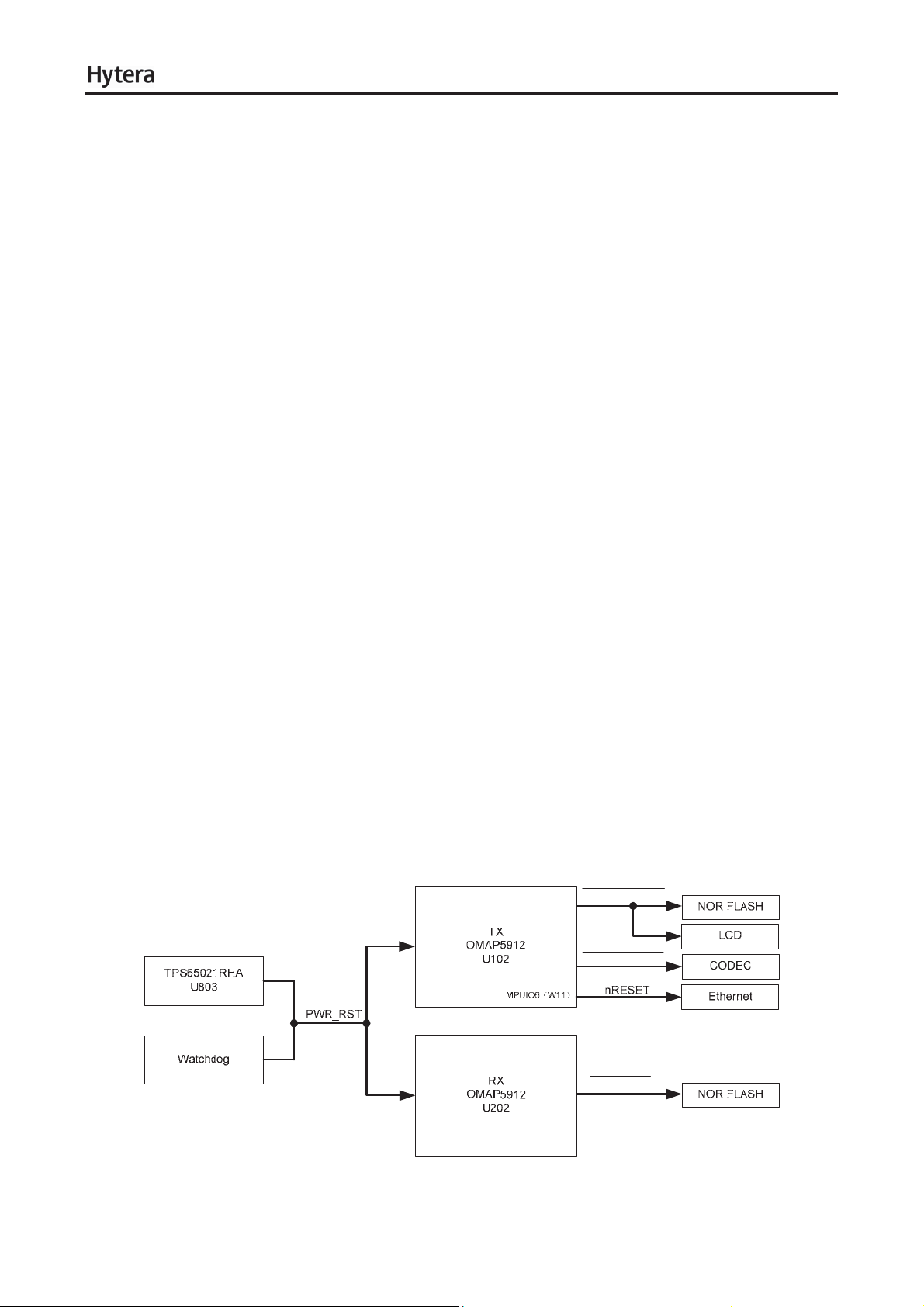
When the system is powered on, PMU will generate a reset signal “PWR_RST” to reset RX OMAP and
TX OMAP. When the system works abnormally, the watchdog will generate a 220ms reset signal as well.
See the following figure:
OUT_TX-RST
CODEC_RST
Figure 6-7 System Reset Block Diagram
12
OUT-RST
Page 16
Service Manual
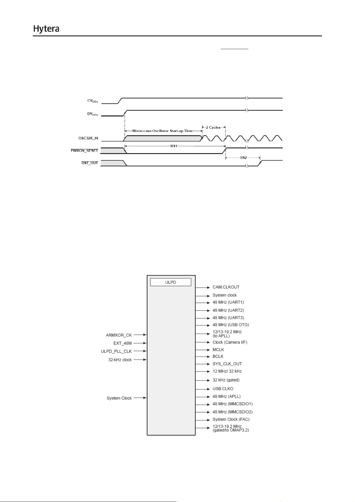
After making response to power-up reset, OMAP5912 will output RST_OUT signal, and maintain low
level for some time to reset the peripheral equipment (NOR Flash) of OMAP. For CODEC chip (U501),
its resetting is subject to MPUIO6 of TX OMAP. The reset sequence of OMAP5912 is shown below:
Figure 6-8 Reset Sequence
6.2.4 Clock
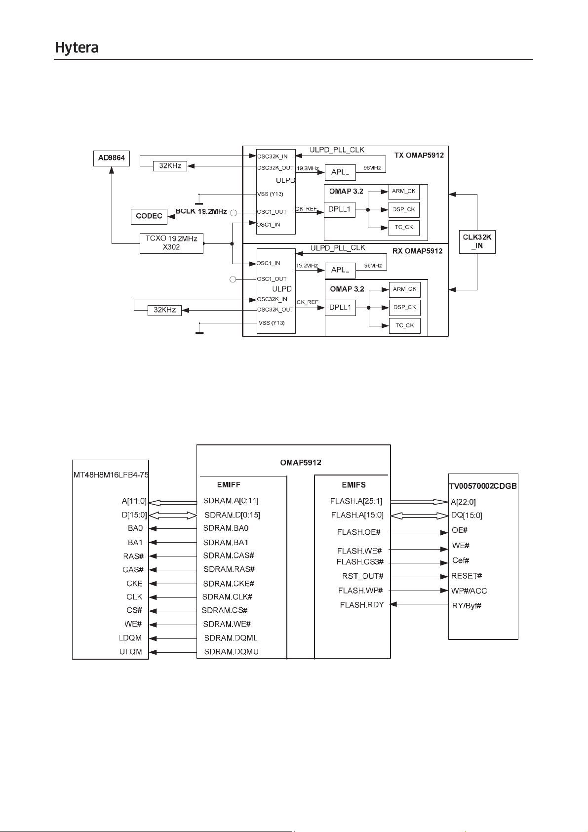
OMAP5912 requires two clocks: system clock and 32K clock. The system clock (12MHz, 13MHz or
19.2MHz) can be provided by an external oscillator or square-wave clock signal. This product’s system
clock is provided by
(Ultralow-power device), which is responsible for OMAP clock management. The clock output by UPLD
is connected to appropriate external interface. See the following figure:
19.2MHz TCXO. Both system clock and 32K clock are provided by ULPD
Figure 6-9 External Clock
13
Page 17
Service Manual
For the built-in and external clock of OMAP2912, there are two reset modes: Reset Mode0 and Reset
Mode1. Reset Mode0 is adopted for this system. As for this product, system clock uses external clock,
while 32K clock uses built-in clock. See the following figure:
Figure 6-10 Clock Connection Block Diagram
6.2.5 Memory
OMAP5912 provides two types of external memory interfaces: external memory interface slow (EMIFS)
and external memory interface fast (EMIFF). External NOR Flash and Mobile SDRAM have been
expanded for two OMAPs in the system. See the following figure:
6-11 Memory Block Diagram
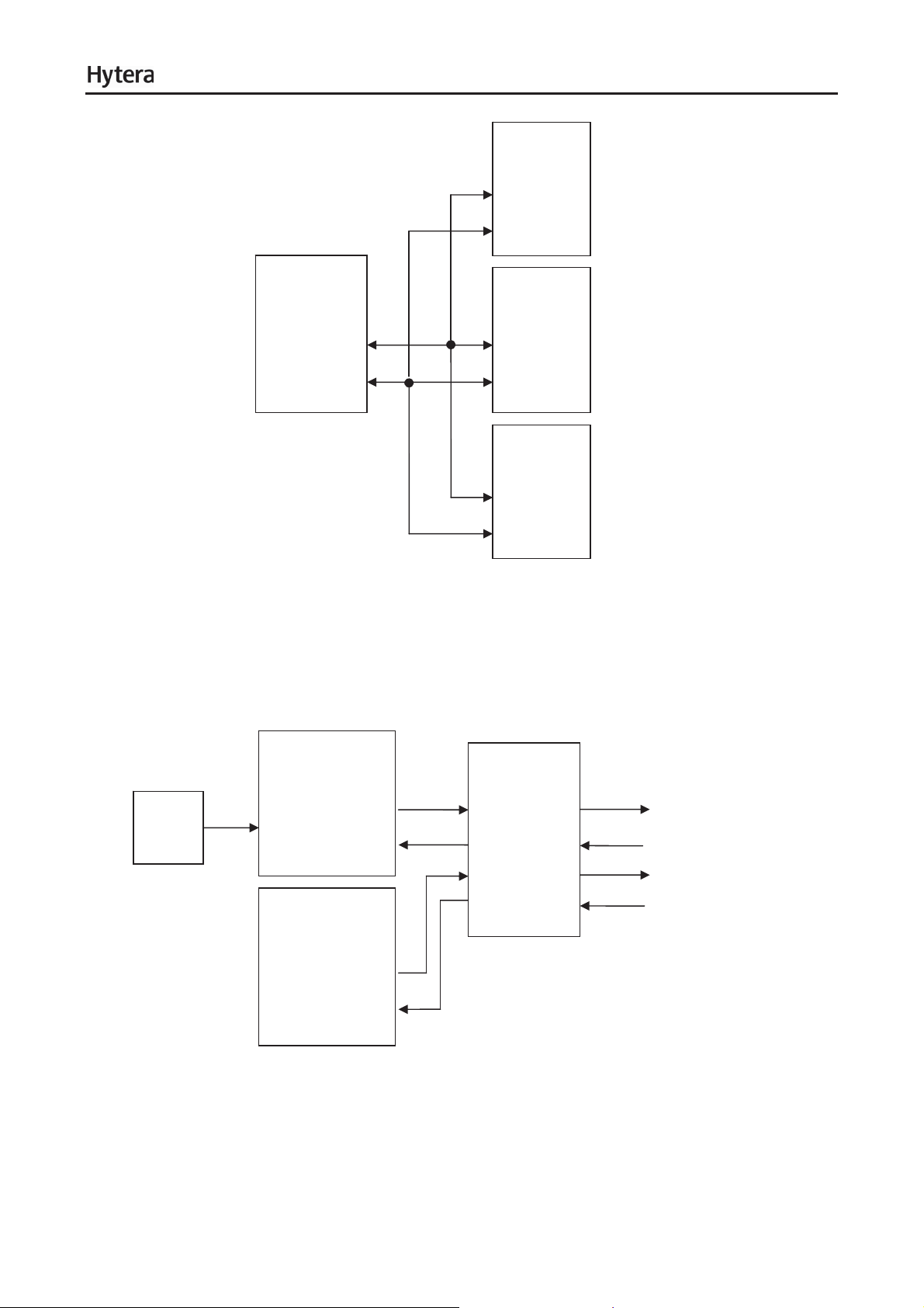
6.2.6 MCBSP
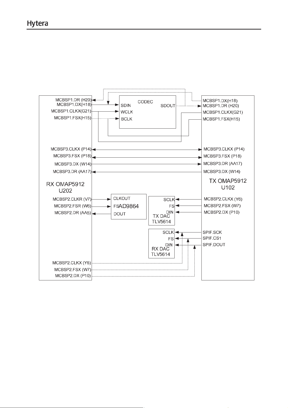
OMAP5912 has 3 McBSP interfaces: McBSP1, McBSP2 and McBSP3. McBSP1 of RX OMAP and TX
OMAP is used to communicate with Codec. RX OMAP McBSP2 is used to connect SSI interface of
14
Page 18
Service Manual
AD9864 to receive demodulation signal from AD9864, and TX OMAP McBSP2 is reserved for SPI
interface of RX DAC TLV5614. McBSP2 of TX OMAP is used to connect SSI interface of TX DAC
TLV5614. TLV5614 works in Slave mode and is managed by DSP. McBSP3 is used to connect RX
OMAP and TX OMAP for data transmission. See the following figure:
Figure 6-12 Diagram of MCBSP Connection
6.2.7 SPI
OMAP5912 has one SPI interface that can connect four SPI components. The descriptions are as follow:
(1) RX OPMAP5912 SPI Interface
The SPI interface of RX OMAP is used to configure IF processor (AD9894) and RX PLL chip
(SKY72310).
AD9894 is controlled by SPI chip select (CS1) of RX OMAP, and RX PLL chip is controlled by CS2. The
connection between RX OMAP SPI interface and AD9894/ RX PLL is shown below:
15
Page 19
3V3D
Service Manual
CS
SKY72310 SCK
Data
3V3D
SPIF.CS2(T19)
SPIF.SCK(U19)
SPIF.DOUT(R18)
RX OMAP5912
U202
PE
AD9864 PC
PD
SPIF.CS1 (N15)
Figure 6-13 RX OMAP SPI Connection Block Diagram
(2) TX OPMAP5912 SPI Interface
TX OMAP SPI is used to configure RX DAC TLV5614 (U303) and TX PLL chip (SKY72310). This chip is
controlled by CS2 and managed by DSP. RX DAC (U303) is controlled by CS1. See the following figure:
KY72310
s
CS
CLK
Data
SPIF.CS2(T19)
SPIF.SCK(U19)
SPIF.DOUT(R18)
OMAP5912
U102
FS
CLK
RX TLV5614 Data
Figure 6-
14 TX OMAP
SPI Connection Block Diagram
SPIF.CS1(N15)
6.2.8 MCSI
MCSI (Multi Channel Serial Interface) belongs to OMAP5912. There are two MCSIs with OMAP5912.
MCSI1 of RX/TX OMAP is reserved for appropriate RX/TX PLL chip to realize modulation feature. See
the following figure:
16
Page 20
Service Manual
˅
˅
CS
TX/RX SKY72310 SCK
Data
MCSI1.SYNC(W8)
MCSI1.CLK(M15)
MCSI1.DOUT(Y
8)
TX/RX OMAP5912
Figure 6-15 Diagram of MCSI Interfac
e
6.2.9 I2C
OMAP5912 provides one I2C interface, and supports communication rate up to 400Kbps. TX OMAP I2C
interface connects with PMU to dynamically adjust PMU voltage output. It works in Master mode. See
the following figure:
TX OMAP5912
U102
I2C.SDA˄V20
I2C.SCL˄T18
Figure 6-
16 Diagram of I
SDAT U803
SCLK
2
C Connection
6.2.10 MICROWIRE
OMAP5912 provides a MICROWIRE interface. The four chip select signals can drive four external
components. MICROWIRE interface signals include: ȝWIRE.CS, ȝWIRE.SCLK, ȝWIRE.SDO and
ȝWIRE.SDI.
In this system, only MICROWIRE interface of TX OMAP is used to connect CODEC and ADC TLV1548.
ȝWire CS0 controls CODEC and ȝWire CS3 controls ADC TLV1548. See the following figure:
17
Page 21

UWIRE.SDO(H19)
UWIRE.SCLK(J15)
UWIRE.SDI(J14)
UWIRE.CS0 (J18)
TX OMAP5912
U102
UWIRE.CS3 (J19)
GPIO37(M19)
GPIO2(D1
Service Manual
TLV320AIC29
U501
MOSI
SCLK
MISO
SS
DATA IN
DATA OUT
I/O CLK TLV1548
U301
CS
EOC
5)
CSTART
Figure 6-17 Diagram of MICROWIRE Connection
6.2.11 USB
OMAP processor provides 3 USB interfaces with rate of 1.5Mbps or 12Mbps. Available modes include
Host and Device. USB0 and USB2 of TX OMAP are used in this system. The description of TX OMAP
USB0 is as follow:
18
Page 22
TX
OMAP5912
U102
USB0_DM(R8)
Service Manual
DB9(J601)
USB_D-
USB_D+
DB26(J701)
USB_D-
USB0_DP(P9)
USB_D+
10pin Jack
USB_D-
USB_D+
Figure 6-18 Diagram of USB Interface
6.2.12 UART
OMAP5912 has 3 UART interfaces: UART1, UART2 and UART3. It supports hardware flow control. The
communication rate can be up to 1.5Mbps. See the following figure:
TX OMAP5912
GPS-XP4
GPS_TX
(TX)
UART1_TXD(Y14)
UART3.RX(K19)
UART1_RXD(V14)
UART3.TX(K18)
MAX3232
T1IN
R1OUT
T2IN
T1OUT
R1IN
T2OUT
TX_Data From Radio
TX_Data to Radio
RX_Data From Radio
RX
OMAP5912
UART1_TXD(Y14)
UART1_RXD(V14)
Figure 6-19 UART Connection Block Diagram
19
R2OUT
R2IN
RX_Data to Radio
Page 23
Service Manual
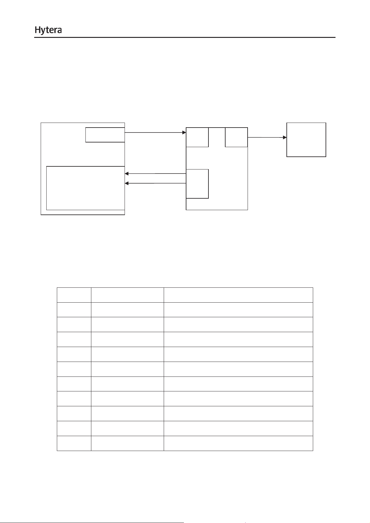
6.2.13 GPS (Reserved)
The system can obtain precise clock signal and related GPS data from the GPS module. The baseband
board connects with the GPS module via J108 and J109. J109 provides GPS module with 5V power
supply. The GPS module provides precise 19.2MHz clock source to exciter board through XS2. See the
following figure:
5V
J109
BASEBAND
GPIO63˄E18˅
UART3.RX˄K19˅
˄TX OMAP U102˅
J108
Figure 6The GPS module adopt
Definitions of GPS module are shown in table below:
Pin No. Name Description
s RS-232 port (baud rate: 9600BPS; 8 data bits; 1 stop bit; no parity check).
GPS-LOCK
TX
20 GPS Module Connection Block Diagram
XP3
XP4
GPS
XS2
19.2MHz
EXCITER
1 GPS-LOCKED GPS RX status
2NC
3NC
4NC
5NC
6NC
7NC
8NC
9 1PPS GPS pulse output
10 NC
Table 6-3 GPS Module Definitions
20
Page 24
Service Manual
6.2.14 Audio Path
The audio path is used to relay audio, output RX audio and input TX audio.
6.2.14.1 Relay Audio Path
After demodulated by AD9864, RX audio in digital/analog mode goes to RX OMAP. Then the audio is
sent to TX OMAP via McBSP3, and finally is subject to DA conversion to modulate VCO.See the
following figure:
AD9864
Q
McBSP2
RX
OMAP5912
U202
McBSP3
TX
OMAP5912
U102
McBSP2
DAC
TLV561
U304
MOD
Figure 6-21 Relay Audio Path
6.2.14.2 RX Audio Path
In digital mode, Codec can co
the left channel and right channel respectively, and select the time slot required for local audio
monitoring via the switch Slot1_EN. Meanwhile, under the control of Slot1_EN and Slot2_EN, the
outputs of Slot A and Slot B are sent to PIN24 and PIN25 of the further development port DB26 (J7
for further development.
In digital mode, SPK1 of CODEC can be configured to
the further development port DB26 (J701). The filtered audio from SPK2 is output to the speaker to
realize local monitoring via the audio amplifier or to the audio port of the front panel via the filter. See the
ntrol the audio output of Slot A from SPK1 and that of Slot B from SPK2 via
01)
output filtered audio or flat audio (RX_Audio) to
following figure:
RX
AD9864
McBSP2
RX
OMAP5912
U202
McBSP3
TX
OMAP5912
U102
McBSP1
CODEC
U501
Figure 6-22 RX Audio Block Diagram
21
Slot1_EN
SPK2
SPK1
RX _Audio_Mute
Slot1_EN
Slot2_EN
Slot A
Slot B
Audio_PA_EN
U502
TDA8547
MMP10_SPK_Audio
RX_Audio
DB26_PIN24
DB26_PIN25
Page 25
Service Manual
6.2.14.3 TX Audio Path
sy em ha wo ds of au sign ls: MM _Ext_Mic
The st s t kin MIC dio a P10_Mic_IN and DB26 _IN. The former is
from the accesso onnected to 10-Pin interface on the front panel, while the latter is from Pin 2 of
the further development port DB26 (J701). The EXT_MIC_C l can d through menu
or programming software to activate MMP10_Mic_IN or DB26_Ext_Mic_IN.
ry c the
TRL
signa be configure
This signal is sent to DSP of
TX OMAP via McBSP1 after processed by CODEC, and is transmitted via the TX circuit after DA
conversion and modulation. See the following figure:
Mod1
Mod2_RFCS
DAC
TLV5614
U304
MCBSP2 MCBSP1
TX
OMAP5912
U102
ADC
CODEC
U501
MMP10_Mic_IN
DB26_Ext_Mic_IN
EXT_MIC_CTRL
Figure 6-23 TX Audio Path
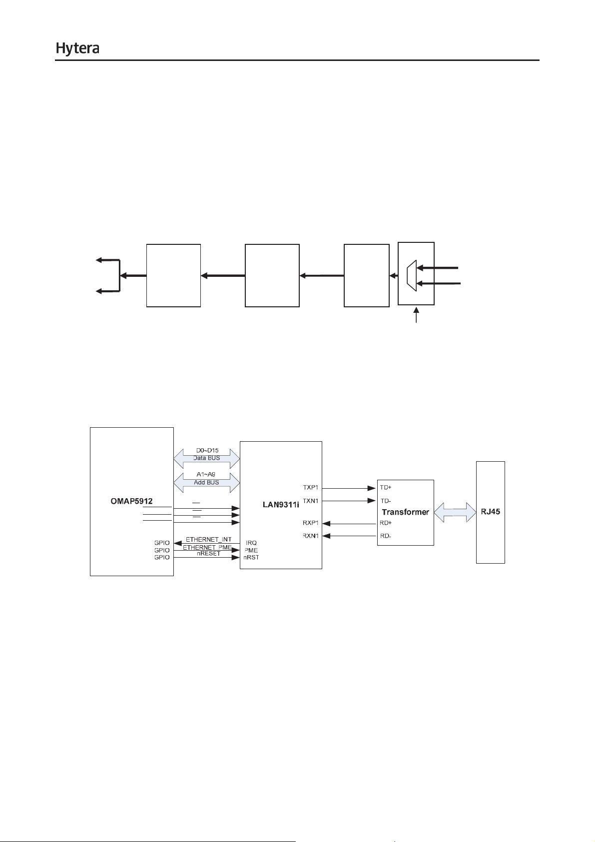
6.2.15 TCP/IP
TCP/IP is used to achieve remote monitoring and other exp
shown as below:
andable functions. The block diagram is
FLASH-OE
FLASH-WE
FLASH-CS0
OE
WR
CS
Figure 6-24 TCP/IP Block Diagram
22
Page 26

S
\
HU
/D
5';3&%9LHZ%DVHEDQG%RDUG
7R
3&%9LHZ
Page 27
\
HU
%RWWRP/D
5';3&%9LHZ%DVHEDQG%RDUG
Page 28
5';3&%9LHZ)URQW3DQHO
7RS/D\HU
Page 29
5';3&%9LHZ)URQW3DQHO
%RWWRP/D\HU
Page 30
TX Unit
g
To AD9864
To RX OMAP
VOL_DET
HT_Alarm
Pout_Check
TX_VCO_Watch
RX_VCO_Watch
,7
RJ45
/&'&6=/&0
72&21752/%2$5'
8
x
a
t
a
d
CS2
6
x
1
a
d
a
t
Ethernet
LAN9311
CS0
EMIFS EMIFF
TX
Control
PLL(TX)
SKY72310
TX DAC
TLV5614
GPIO
MCSI
CS2
SPI
M
c
B
2
P
S
X
T
McBSP2
McBSP3
3
P
S
B
c
M
32MB
Mobile SDRAM
79&'*%
6
1
x
a
t
a
d
07+0/)%
CS3
6
1
x
a
t
a
d
DSP
TMS320C55x
McBSP1
GPIO
McBSP1
IIS
Synchronous Timing
VSWR_Check
19.2MHz
19.2MHz
JTAG
TCXO
ADC
19.2MHz
TLV1548
32KHz
CS3
CLK
JTAG
uWire
TX OMAP5912
MCLK
PWM0/PWT
19.2MHz
19.2MHz
GPS BOARD
EXT BOARD
TX
GPS-LOCK
GPIO
UART3
UART1 US B
GPIO
MPU
ARM926EJ-S
GPIO
uWire
Program_ I/O
TX OMAP
Data Bus From
GPIO
MPUIO/
GPIO
Program_ I/O
USB
SW update
(DB9/DB26)
User program
RS-232
(CON5)
74HC594
EMIFS
74HC594
Connector
FAN1/FAN2
LCD
LED
FRONT PANEL
Key/knob
MMP10
MIC
27
Slot1/Slot2
CS0
SPI
RX Audio
Audio
preamp
RX FlatǃFiltered Audio/SlotAǃSlotB Audio
Mic
Audio Codec
TLV320AIC29
Filted/Flat Audio
preamp
DB26
TDA8547S
Speaker
1
P
S
B
c
M
GPIO
McBSP1
DSP
TMS320C55x
RX OMAP5912
CLK
JTAG
6
1
x
a
t
a
d
32MB
Mobile SDRAM
07+0/)%
32KHz
19.2MHz
32KHz
From 19.2MHz TCXO
JTAG
,7
MPU
ARM926EJ-S
UART1
RS232
(Con5)
ram
RD980 ᏺ⧚Ḛ
RD98X Block Diagram (Baseband Section)
RX Unit
CS1
RX DAC
TLV5614
R
X
M
P
c
S
2
SSI
AD9864
IF processor
SPI
SI
PLL(RX)
SKY72310
RX
Control
B
CS1
CS2
McBSP3
McBSP2
SPI
MCSI
GPIO
EMIFS EMIFF
6
1
x
a
t
CS3
a
d
79&'*%
6.4 Block Dia
Page 31

5VA
CODEC_AVDD(10mA)
3.3VA
RP102N331D
TCXO(2mA)
28
(300mA)
ADC TLV1548_AVDD(5mA)
DAC 5610/5604_AVDD10mA)
WTD
timer
OMAP Core_TX
CVDD1.2.3
CVDDRTC/CVDDDLL
(250mA)
OMAP Core_RX
CVDD1.2.3
CVDDRTC/CVDDDLL
OMAP DVDD (1.2.3.5.6.7.8.9)
DVddrtc(50mA*2)
OMAP Perpherial(10mA*2)
FLASH(50mA*2)
Indication LED(20mA*2)
DAC 5610/5604(5mA)
Shift/store register(5mA)
EthernetVDD33IO/VDD33A1/VDD33A2
CODEC_DigIO(5mA)
MAX3232(5mA)
CODEC Core(10mA)
CODEC_VREF(15mA)
SDRAM(85mA*2)
OMAPDVDD4(10mA*2)
EthernetVDD18CORE/VDDTX1/VD
OMAP TX/RX /MPU_RST
/PWRON_RST
DTX2/VDD18PLL
(250mA)
TX Board
Audio_PA
Accessory
Connectory(1A)
RD98X Block Diagram (Power Supply Section)
RD980ᏺ⬉⑤Ḛ
12.6V(1A)
2SB1184
B+
13.6V+/-15%
Vehicle Power In
Audio_OpAmP(20
mA)
Excite Board
Recive Board
(300mA)
XC6209E502PR
MAP Accessory
VBUS_SW
(500mA)
9V3A(700mA)
LM2941T(1A)
(5mA)
TPS5431(3A)
3V3D
1V8D
1V6D
/RESPWON
VDCDC2(1A)
VDCDC1(1.2A)
VDCDC3(0.9A)
PMU TPS65021
Controller
header(200mA)
Audio_PA(200mA
)
5V_GPS
GPS
TPS5431(3A)
connector(500mA
)
Page 32

1
1
KAA-3528RG
KAA-3528RG
KAA-3528RG
KAA-3528RG
150R9150
R9
43
ALARMD8ALARM
R11
R11
1
2
1
C7
3
Q5
470pC6470p
21
D10
D10
D9
21
43
KAA-3528RGD9KAA-3528RG
R13
R13
TP7TP7
1
150
150
3
Q6
2
DTC114EEQ5DTC114EE
1
C8
470pC7470p
TP8TP8
150
150
Q7
2
DTC114EEQ6DTC114EE
1
C9
470pC8470p
43
21
D12
D12
D11
D11
21
43
1
3
DTC114EEQ7DTC114EE
470pC9470p
KAA-3528RG
KAA-3528RG
DTC114EEQ8DTC114EE
Q8
2
1
C11
C11
RED
3
1
2
Q11
Q11
DTC114EE
DTC114EE
3
1
470p
470p
C12
C12
C141uC14
470p
470p
TP49TP49
R14 10KR14 10K
3V3D
R15 1KR15 1K
1
PWR_LED_CTRL
C131uC13
R17
R17
3
2
R16 1KR16 1K
5VD5VD
200R8200
R8
R7
200R7200
150R6150
R6
D8
12
5VD
D7
5VD
5VD
12
D5
RX-AD5RX-A
D6
R4
12
TX-BD6TX-B
R5
1
TP4TP4
150R4150
RX-BD7RX-B
TP6TP6
150
150
R10
R10
TP5TP5
1
150R5150
3
DTC114EEQ4DTC114EE
Q4
3
2
12
5VD
D4
TX-AD4TX-A
12
5VD
2
TP3TP3
D3
AnalogD3Analog
1
Q3
DTC114EEQ3DTC114EE
150R3150
R3
3
2
DTC114EEQ2DTC114EE
Q2
1
C1
1
2
C6
1
470pC2470p
C2
470pC1470p
12
5VD
TP2TP2
3
12
5VD
D1
RPDD1RPD
12
5VD
1
D2
DigitalD2Digital
180R2180
R2
3
TP1TP1
1
Q1
DTC114EEQ1DTC114EE
R1
150R1150
3
2
ࠡ䴶ᵓ⧚
RD980
5';6FKHPDWLF'LDJUDP)URQW3DQHO&LUFXLW
4
5
Repeater Disable_LED
3
Digital_LED
C49
C49
C48
C48
C47
C47
C46
C46
TX-A_LED
Analog _LED
U1
74AHCT594PW
U1
74AHCT594PW
0.1uF
0.1uF
D420
D420
1
MMBZ5V6ALT1G
MMBZ5V6ALT1G
2
100pF
100pF
100pF
100pF
100pF
100pF
1
15
QB
QA
QC2QD
RCLK12/RCLR13SER
14
LED_S/P_EN
PRST
LED_S/P_DAT
TX-B_LED
RX-A_LED
5
4
3
6
QF
QE
11
16
R41 10KR41 10K
3V3D
LED_S/P_CLK
QG
VCC
7
QH
GND8QH'9/SRCLR10SRCLK
RX-B_LED
C51
0.1uF
C51
0.1uF
C50
100pF
C50
100pF
ALARM_LED
6FKHPDWLF'LDJUDP
GRN
1u
1u
100K
100K
Q10
Q10
2
Q9
1
DTC114EE
DTC114EE
TP45TP45
1
2
D24
D24
1
5VD
1
DTC114EEQ9DTC114EE
3V3D
42
J2
MMBZ6V8ALT1G
MMBZ6V8ALT1G
3
C53
100pF
C53
100pF
BLM18PG300SN1
BLM18PG300SN1
L2
L2
1
TP47TP47
1
TP46TP46
1
TP17TP17
1
TP16TP16
1
TP15TP15
1
TP14TP14
1
TP13TP13
1
TP12TP12
1
TP11TP11
1
TP10TP10
1
TP9TP9
1
TP18TP18
1
TP19TP19
1
TP20TP20
R49
R49
R51
R51
R37
R37
R50
R50
1
TP24TP24
1
TP23TP23
1
TP22TP22
1
TP21TP21
X1A1X2A2X3A3X4A4X5A5X6
Y1C1Y2C2Y3C3Y4C4Y5C5Y6
U7 CM1440U7 CM1440
LED_S/P_CLK
5VD5VD 5VD
BACKLIGHT
GND2
S/P_CSLED
S/P_CLOCK25S/P_DATA26 WE_LCD
24
PRST
10K
10K
10K
10K
10K
10K
10K
10K
CM1440U6CM1440
A6
GND3
GND2
GND1
C6
LED_S/P_EN
LED_S/P_DAT
CH+
D15
D15
12
KPT-1608SGC
KPT-1608SGC
p1
12
D14
D14
KPT-1608SGC
KPT-1608SGC
P4
12
D13
D13
KPT-1608SGC
KPT-1608SGC
CS2_LCD29F_A1_LCD30F_D7_LCD31F_D6_LCD32F_D5_LCD33F_D4_LCD34F_D3_LCD35F_D2_LCD36F_D1_LCD37F_D0_LCD38 OE_LCD
28
27
X1A1X2A2X3A3X4A4X5A5X6
U6
Y1C1Y2C2Y3C3Y4C4Y5C5Y6
B3
B2
B1
J1
D18
D18
CH-
12
KPT-1608SGC
KPT-1608SGC
p2
12
D17
D17
KPT-1608SGC
KPT-1608SGC
p3
12
D16
D16
KPT-1608SGC
KPT-1608SGC
X1A1X2A2X3A3X4A4X5A5X6
Y1C1Y2C2Y3C3Y4C4Y5C5Y6
U5 CM1440U5 CM1440
A6
GND3
B3
GND2
B2
GND1
B1
C6
19
22
21
DB818DB9
DB1020DB11
DB1323DB1424DB1525DB1626DB17
DB112
17
R2456R24
56
R2656R26
56
R2356R23
56
ACC_ID3USB_VBUS4MMP_PRGM_IO4
KNOB_A10KNOB_B
VOL_GPIO113VOL_GPIO214KNOB_C
BACKLED_CTRL
PRST175VD40GND39KB_C018KB_C119KB_C220KB_R021KB_R122PWR_LED
11
15
16
MMP_PRGM_IO3
6
23
PWR_LED_CTRL
1
VOL_GPIO1
VOL_GPIO2
BACKLED_CTRL
1
1
A6
GND3
B3
GND2
B2
GND1
B1
1
C6
1
TP32TP32
TP31TP31
TP30TP30
1
1
1
R46 10KR46 10K
10K
10K
R36
R36
10K
10K
R35
R35
10K
10K
R34
R34
3V3D
C19
C19
C52
C52
C17
C17
R28 51R28 51
R27 51R27 51
R25 51R25 51
LED_A
LED_K132LED_K233LED_K3
Q13
Q13
2
U2
100p
100p
100p
100p
0.1uf
0.1uf
C18
100p
C18
100p
100p
100p
C30
C30
34
C34
C34
GND1VCI12VCI23IOVCC4FLM5CS6RS7 WR8 RD9DB010DB111DB212DB313DB414DB515DB616DB7
CSZLCM1830J1CSZLCM1830
C16
100p
C16
100p
C15
C15
0.1uf
0.1uf
BACKLED_CTRL
2SK1824
2SK1824
2
A4B
S2
S1
1
31
Q12
Q12
100p
100p
1
TP48TP48
R22 0R22 0
27
28
3V3D
30
IM329IM0
RESET
31
R43 10KR43 10K
31
3V3D
INT_MIC
MIC_GROUND
HANDSET_AUDIO
7
2
1
12
TP25TP25
TP26TP26
TP27TP27
100pf
100pf
C24
C24
TP28TP28
100pf
100pf
C28
C28
TP29TP29
100pf
100pf
C29
C29
C44
C44
C43
C43
R47 10KR47 10K
R48 10KR48 10K
5
KNOBU2KNOB
C
3
2
2SK1824
2SK1824
R39 33R39 33
BACKLED_CTRL
3V3D
U4
XC6209E332PR
U4
XC6209E332PR
5VD
GND1
41
con40J2con40
USB_D-
USB_D+8MMP_PRGM_IO0
5
9
S3P4S3
S2P3S2
S1
0.47uF
0.47uF
0.47uF
0.47uF
C42
0.47uF
C42
0.47uF
0
R290R29
10K
10K
R40
R40
3V3D
R30 0R30 0
C27
1uf
C27
1uf
1
5
Nc
Vout
Vin4Vss2CE
3
C26
1uF
C26
1uF
+
+
12
C25
C25
22uF/10V
22uF/10V
L1
L1
BLM18PG300SN1
BLM18PG300SN1
100pf
100pf
C22
C22
100pf
100pf
C23
C23
D22
MMBZ6V8ALT1G
D22
MMBZ6V8ALT1G
4
2
S2
S1
1
3
D21
D21
D20
D20
D19
D19
MMBZ5V6ALT1G
MMBZ5V6ALT1G
U8
U8
PRTR5V0U2X
PRTR5V0U2X
VOL_GPIO1
VOL_GPIO2
R45 10KR45 10K
R44 10KR44 10K
5
A4B
C
3
2
1
C39
C39
C36
100pf
C36
100pf
MMBZ20V
MMBZ20V
C35
C35
C38
C38
MMBZ5V6ALT1G
MMBZ5V6ALT1G
C37
C37
C32
C32
C31
C31
C45
100pf
C45
100pf
C33
C33
2 3
1
R310R31
NC
no use
C41
C41
0.47uF
0.47uF
C40
0.47uF
C40
0.47uF
E27U3E27
100pf
100pf
100pf
100pf
100pf
100pf
100pf
100pf
100pf
100pf
100pf
100pf
100pf
100pf
0
2
1
ACC_ID
GPIO3_PTT
J3
1
TP44TP44
1
TP43TP43
3
4
3
4
5
5
S6P1S6
P4
1
2
3
4
1
2
3
4
1
2
P1
1
2
3
4
5
5
S5P2S5
P3
P2
1
2
3
4
5
5
S4
CH-S4CH-
CH+S1CH+
1
2
5VD
R42
10K
R42
10K
100PF
100PF
C21
C21
10K
10K
R33
R33
10K
10K
3V3D
R32
R32
U3
100PF
100PF
C20
C20
BLM15AG121SN1
BLM15AG121SN1
L417
L417
1 2
7
3
6
5
4
USB_D-
INT_MIC
USB_VBUS
MIC_GROUND
HANDSET_AUDIO
1
1
1
1
1
1
1
1
1
1
2
1
BLM15AG121SN1
BLM15AG121SN1
L418
L418
CM2-2012MCIN-181T
CM2-2012MCIN-181T
L416
L416
3 4
8
10
9
USB_D+
GPIO4_HOOK
CON10_MMPJ3CON10_MMP
GPIO0_PWR ON
TP33TP33
TP34TP34
TP35TP35
TP36TP36
TP37TP37
2
TP38TP38
TP39TP39
TP40TP40
TP41TP41
TP42TP42
3
D23
MMBZ6V8ALT1G
D23
MMBZ6V8ALT1G
3
4
5
D D
C C
B B
A A
Page 33

TP813TP813
1
D810
D805
MMBZ6V8ALT1G
D805
MMBZ6V8ALT1G
5VD
C807NCC807
NC
1
TP806TP806
2
3
5'ᏺЏᵓ⧚˄⬉⑤⬉䏃˅
5';6FKHPDWLF'LDJUDP%DVHEDQGB3RZHU6XSSO\&LUFXLW
4
1
12
L803
L803
8
PH
VIN
U801
TPS5431DDA
U801
TPS5431DDA
7
L805
L805
+
+
C812
C812
12
C806
C806
+
C809
+
C809
12
R803
R803
+
C813
+
C813
15uH
15uH
C7121nC712
D801
D801
C803
C803
0.01uF
0.01uF
NC2NC
R801
R801
12
10uH
10uH
NC
NC
0.1uF
0.1uF
22uF/10V
22uF/10V
68K/F
68K/F
220uF/10V
220uF/10V
1n
B340A
B340A
1 2
1
BOOT
3
100K
100K
C808
0.01uF
C808
0.01uF
C805
1uF/25V
C805
1uF/25V
+
+
C804
C804
C862
1uF/25V
C862
1uF/25V
C863
0.01uF
C863
0.01uF
4
VSENSE
EN5GND
6
C802
C802
R802
R802
47uF/25V
47uF/25V
R806
R806
PowerPAD
9
1000pF
1000pF
22K
22K
22K/F
22K/F
3VRTC
5VD
3V3D
L801
L801
BLM18PG181SN1D
BLM18PG181SN1D
12
12
C817
2.2uF/10V
C817
2.2uF/10V
31
PWRFAIL
U803
U803
TPS65021RHA
TPS65021RHA
VCC37PWRFAIL_SNS
L825
L825
BLM18PG181SN1D
BLM18PG181SN1D
R81510R815
D810
C873
C873
C872
C872
+
+
C828
C828
+
+
16
21
LOWBAT
VINDCDC1
6
36
10
12
B802B802
D802
D802
+
+
12
C811
C811
C810
C810
1 2
MR2835SKG
MR2835SKG
330uF/35V
330uF/35V
470p/50V
470p/50V
L802
L802
BLM41PG600SN1
BLM41PG600SN1
5
1 2
L807
L807
B+
B801B801
J801
J801
13.6V
D803
D803
ZSH5MA27
ZSH5MA27
1
2
JK_PWR
JK_PWR
D D
MMBZ5V6ALT1G
MMBZ5V6ALT1G
1uF
1uF
0.01uF
0.01uF
C865
C865
68uF/6.3V
68uF/6.3V
22uF/10V
22uF/10V
L824 22uHL824 22uH
47K
47K
R819
R819
7
9
24
25
L1
VRTC
VDCDC1
DCDC2_EN
DCDC1_EN
VINDCDC3
VINDCDC2
LOWBAT_SNS
5
38
39
R840 100KR840 100K
R817
R817
C827
C827
+
+
12
C856
C856
+
+
12
C823
C823
+
+
12
C826
C826
TP801TP801
R816
R816
470K/F
470K/F
12
BLM41PG600SN1
BLM41PG600SN1
C C
TP814TP814
1
D811
D811
MMBZ5V6ALT1G
MMBZ5V6ALT1G
1V8D
C875
C875
C874
C874
L823
L823
BLM18PG181SN1D
BLM18PG181SN1D
C869
C869
+
+
12
C829
C829
+
+
12
L826 22uHL826 22uH
C857
C857
19
35
33
22
23
L2
VINLDO
VDCDC2
DCDC3_EN
HOT_RESET11DEFLDO112DEFLDO213VSYSIN14VBACKUP
TRESPWRON
26
C801 0.01uFC801 0.01uF
R846 100KR846 100K
R844
R844
100k
100k
100k
100k
R818
R818
100K
100K
1uF/25V
1uF/25V
10uF/10V
10uF/10V
10uF/10V
10uF/10V
10uF/10V
10uF/10V
VOL_DET
1uF
1uF
0.01uF
0.01uF
68uF/6.3V
68uF/6.3V
R842
R842
22uF/10V
22uF/10V
L821 6.2uHL821 6.2uH
1uF
1uF
18
20
VLDO2
VLDO1
LDO_EN
100K
100K
4
2
L3
VDCDC3
DEFDCDC1
10
PWR_RST
12
D807
D807
4.7K
4.7K
R821
R821
27
28
INT
RESPWON
DEFDCDC3
DEFDCDC2
1
32
1
D809
D809
UDZSTE(175.1B)
UDZSTE(175.1B)
1 2
R820
100K
R820
100K
C830
C830
1000P
1000P
I2C_SCL
I2C_SDA
MBRM120LT1G
MBRM120LT1G
R836 4.7KR836 4.7K
17
40
29
30
SCLK
SDAT
AGND1
PGND1
PGND2
3
8
15
34
R845
R845
13V6A
F803
F803
TP802TP802
Q802
Q802
L814
L814
TP815TP815
1
D812
D812
1V6D
C877
C877
C876
C876
L822
L822
BLM18PG181SN1D
BLM18PG181SN1D
+
+
12
+
+
12
C846
C846
41
PAD
AGND2
R8330R833
PGND3
10k
10k
C859
47uF/25V
C859
47uF/25V
+
+
12
LITTELFUSE0466002
LITTELFUSE0466002
C832
1000P
C832
1000P
1
2SB1184
2SB1184
3 2
R849
R849
12
BLM41PG600SN1
BLM41PG600SN1
MMBZ5V6ALT1G
MMBZ5V6ALT1G
1uF
1uF
0.01uF
0.01uF
C871
C871
68uF/6.3V
68uF/6.3V
R843
200K
R843
200K
22uF/10V
22uF/10V
0
31
Q803
Q803
2SK1824
2SK1824
R839 1KR839 1K
1
47K
47K
R841
R841
2
R850 1KR850 1K
PWR_ON
B B
120K
120K
9V3A
5VA
TP803TP803
U821
U821
L819
L819
12
D808
D808
MBRM120LT1G
MBRM120LT1G
R848 0R848 0
6
8
7
/RST
WDO
MR1VCC2GND3PFI
U805
U805
R814 0R814 0
R823 0R823 0
3V3D
TP805TP805
1
3V3A
L820
L820
BLM18PG181SN1D
BLM18PG181SN1D
5
VOUT
U806
U806
VDD1GND2CE
RP102N331B
RP102N331B
1
TP804TP804
BLM18PG181SN1D
BLM18PG181SN1D
VOUT
5
VIN
4
U807
U807
+
+
C836
10uF/16V
C836
10uF/16V
12
0.1u
0.1u
C835
C835
1
470P
470P
C834
C834
R829
4.32k/F
R829
4.32k/F
1
5
ADJ
OUT
GND
LM2941S
LM2941S
ON/OFF
IN
2
4
0.1u
0.1u
C837
C837
12
L816
L816
BLM41PG600SN1
BLM41PG600SN1
F802
F802
MINISMDC110F
MINISMDC110F
RST_CTRL
5
WDI
PFO
TPS3705-33DGN
TPS3705-33DGN
4
0.1u
0.1u
C878
C878
220p
220p
C840
C840
0.1u
0.1u
C839
C839
C838
2.2uF/10V
C838
2.2uF/10V
4
NC
3
C842
C842
2.2uF/10V
2.2uF/10V
0.1u
0.1u
C864
C864
+
+
12
C819
C819
22uF/10V
22uF/10V
XC6209F502PR
XC6209F502PR
R831
R831
3
NP(VREF)
GND
ON/OFF
681/F
681/F
1
2
3
R832
R832
C844
C844
C845
C845
47K
47K
TP807TP807
0.1u
0.1u
1000p
1000p
5V_GPS
U802
U802
12
1
12
C814
C814
12
L804
L804
15uH
15uH
D804
D804
C843
C843
8
PH
VIN
TPS5431DDA
TPS5431DDA
7
L813
L813
10uH
10uH
12
L815
L815
BLM41PG600SN1
BLM41PG600SN1
D806
D806
C822NCC822
+
+
C831
C831
C821
C821
+
C833
+
C833
R804
R804
+
+
C7001nC700
0.01uF
0.01uF
NC2NC
R808
R808
12
C861
C861
MMBZ6V8ALT1G
MMBZ6V8ALT1G
NC
NC
NC
0.1uF
0.1uF
22uF/10V
22uF/10V
68K/F
68K/F
220uF/10V
220uF/10V
1n
B340A
B340A
1 2
1
BOOT
EN5GND
3
100K
100K
C815
0.01uF
C815
0.01uF
C820
1uF/25V
C820
1uF/25V
+
+
C816
C816
47uF/25V
47uF/25V
C860
1uF/25V
C860
1uF/25V
0.01uF
0.01uF
A A
4
VSENSE
PowerPAD
6
9
C841
C841
R805
R805
R807
R807
1000pF
1000pF
22K
22K
22K/F
22K/F
1
2
3
4
5
Page 34

1
4
23
B+
1
3
D601
D601
L615
L615
BAV70
BAV70
1
1 2
BLM41PG600SN1
BLM41PG600SN1
2
2
MMP_PRGM_IO4
MIC_GROUND
MMP10_Mic_IN
MMP_ACC_IO1
V_BUS
R6240R624
3V3D
MMP_PRGM_IO3
USB0_D+
USB0_D-
470p
470p
2200UF
2200UF
+
+
1 2
C638
C638
C639
C639
0
10K
10K
R322
R322
J103
J103
MMP_PRGM_IO0
KNOB_A
KNOB_B
MMP10_SPK_AUDIO
VOL_GPIO2
VOL_GPIO1
D605
BAV70
D605
BAV70
3
C146
C146
R137 33R137 33
123
JK_FAN1
JK_FAN1
/RST-OUT_TX
KB_C1
KB_C0
KNOB_C
BACKLED_CTRL
KB_C2
32
47K
47K
R629
R629
2
1
100p
100p
Q605
Q605
3
R437 10KR437 10K
3V3D
R438 10KR438 10K
FAN_STOP_DET
LED_S/P_EN
DC_PWR_LED_CTRL
KB_R0
KB_R1
Q921
Q921
PZT2222AT1
PZT2222AT1
Q601
2SB1132
Q601
2SB1132
1
R627
R627
3
2
DTC114EE
DTC114EE
1
/OE_LCD
/WE_LCD
S/P_CLK
S/P_DAT
BLM18PG300SN1
BLM18PG300SN1
33R
33R
2
FAN1
CS2_LCD
F_A1_LCD
DTC114EE
Q603
DTC114EE
Q603
1
1.5K
1.5K
R628
R628
F_D7_LCD
F_D6_LCD
F_D5_LCD
R811NCR811
F_D4_LCD
F_D3_LCD
F_D2_LCD
NC
F_D1_LCD
F_D0_LCD
D608D608
2
1
5VD
4
5V_GPS
C649
C649
C650
C650
D604
D604
PRTR5V0U2X
PRTR5V0U2X
100p
100p
100p
100p
4 3
5
6
TP219TP219
TP218TP218
TP217TP217
1
2 3
J601
J601
12345
678
1
1
1
0
0
R6520R652
R6510R651
TX_PLL_CS2_DB9
TX_PLL_CLK_DB9
0
NC
R6180R618
R617NCR617
V_BUS
USB0_D-
9
0
R6530R653
TX_PLL_Data_DB9
2
S601S601
1
S602S602
1
0
NC
R6470R647
R619 0R619 0
R649NCR649
USB0_D+
BOOT_DOUT_TX
BOOT_DOUT_RX
2
JK_DB9
JK_DB9
C648
100p
C648
100p
C611
1000p
C611
1000p
C610
100p
C610
100p
C609
100p
C609
100p
C646
100p
C646
100p
C647
100p
C647
100p
D607
D607
MMBZ20V
MMBZ20V
3
3
NC
0
R650NCR650
R6480R648
BOOT_DIN_TX
BOOT_DIN_RX
1
2
10K
10K
R632
R632
3
5';6FKHPDWLF'LDJUDP%DVHEDQGB,QWHUIDFH&LUFXLW
5'ᏺЏᵓ⧚˄ষ⬉䏃˅
4
3V3D
R633
R633
R601NCR601
10K
10K
C608
C608
C607
C607
C606
C606
C605
C605
C604
C604
C603
C603
C602
C602
C601
C601
L611 BLM18PG300SN1L611 BLM18PG300SN1
L612 BLM18PG300SN1L612 BLM18PG300SN1
L613 BLM18PG300SN1L613 BLM18PG300SN1
L610 BLM18PG300SN1L610 BLM18PG300SN1
L609 BLM18PG300SN1L609 BLM18PG300SN1
R610 0R610 0
C636 100pC636 100p
C635 100pC635 100p
C634 100pC634 100p
C633 100pC633 100p
C632 100pC632 100p
C631 100pC631 100p
C630 100pC630 100p
C629 100pC629 100p
C628 100pC628 100p
C627 100pC627 100p
C626 100pC626 100p
C625 100pC625 100p
C624 100pC624 100p
C623 100pC623 100p
C622 100pC622 100p
C621 100pC621 100p
C620 100pC620 100p
C619 100pC619 100p
C618 100pC618 100p
C617 100pC617 100p
C616 100pC616 100p
C615 100pC615 100p
C614 100pC614 100p
C613 100pC613 100p
C612 100pC612 100p
3V3D
U601
U601
J603
J603
6
1
R620 4.7KR620 4.7K
1
5
2
2
DC_PWR_DET
DC_PWR_DET
DC_PWR_DET
DC_PWR_LED_CTRL
R622 1KR622 1K
R623 0R623 0
TIL113
TIL113
3 4
R6211KR621
1K
L607 BLM18PG300SN1L607 BLM18PG300SN1
L608 BLM18PG300SN1L608 BLM18PG300SN1
L606 BLM18PG300SN1L606 BLM18PG300SN1
L604 BLM18PG300SN1L604 BLM18PG300SN1
L602
L602
L605 BLM18PG300SN1L605 BLM18PG300SN1
L603 BLM18PG300SN1L603 BLM18PG300SN1
R604 0R604 0
R602 0R602 0
R603 0R603 0
R605 NCR605 NC
100p
100p
100p
100p
100p
100p
100p
100p
100p
100p
100p
100p
100p
100p
100p
100p
R608 33R608 33
R609 33R609 33
R606 33R606 33
R607 33R607 33
NC
R616 33R616 33
R615 33R615 33
R614 33R614 33
R612 33R612 33
R611 33R611 33
R613 33R613 33
3
4
6
5
1
2
43
5
D603D603
6
5
1
2
5
43
123456789101112131415161718192021222324252627282930313233343536373839
J602
J602
D D
C C
D602D602
40
HEAD
HEAD
B B
A A
Page 35

10K
10K
34
R730
R730
R724
10K
R724
10K
25
1
1
R725
R725
R723
R723
10K
10K
10K
10K
34
25
1
R2
R2
R1
R1
R1
R1
R2
R2
R1
R1
R2
R2
6
R2
R2
R1
R1
6
C710
C710
Q710
Q710
MUN5214DW1T1
MUN5214DW1T1
C711
C711
Q709
Q709
MUN5214DW1T1
MUN5214DW1T1
220p
220p
220p
220p
D707
D707
MMBZ20V
MMBZ20V
1
5VD 5VD 5VD
R722
10K
R722
10K
34
R2
5VD 5VD 5VD
R719
R719
10K
10K
25
1
R2
R1
R1
R1
R1
Q707
R2
R2
6
Q707
MUN5214DW1T1
MUN5214DW1T1
5VD
R718
10K
R718
10K
1
R2
R2
R1
2
25
34
R716
10K
R716
10K
5VD
R1
R1
R1
R2
R2
6
Q708
Q708
MUN5214DW1T1
MUN5214DW1T1
R796
R796
R795
R795
470
470
33K
33K
34
R2
5VD
R715
R715
10K
10K
25
1
R2
R1
R1
R1
R1
R2
R2
6
Q706
Q706
MUN5214DW1T1
MUN5214DW1T1
5VD5VD5VD
470
R711
R711
10K
10K
1
R2
R2
R1
25
34
10K
10K
R710
3
R710
1
25
R714
R714
R713
R713
R717
R717
10K
10K
10K
10K
3.9K
3.9K
34
1
25
34
34
25
1
R731
R731
10K
10K
R732
R732
10K
10K
R708
R708
10K
10K
R709
R709
10K
10K
R706
R706
10K
3V3D
R705
R705
R704
R704
R703
R703
R702
R702
10K
10K
10K
10K
10K
10K
10K
10K
10K
5VD
5VD
5'ᏺЏᵓ⧚˄'%ষ⬉䏃˅
5';6FKHPDWLF'LDJUDP%DVHEDQGB'%,QWHUIDFH&LUFXLW
4
R1
R1
R1
R2
R2
R2
R2
R1
R1
R1
R1
R2
R2
R2
R2
R1
R1
R1
R1
R2
R2
R2
R2
R1
R1
R1
R1
R2
R2
6
Q705
Q705
6
Q704
Q704
6
Q703
Q703
R798 3.9KR798 3.9K
6
470
R794
R794
33K
33K
R793
R793
470
470
R792
R792
33K
33K
R791
R791
R790
470
R790
470
33K
33K
R789
R789
MUN5214DW1T1
MUN5214DW1T1
Q702
Q702
MUN5214DW1T1
MUN5214DW1T1
C709
C709
C708
C708
C707
C707
C706
C706
D704
D704
C705
C705
MUN5214DW1T1
MUN5214DW1T1
C704
220p
C704
220p
MUN5214DW1T1
MUN5214DW1T1
D703
D703
C703
C703
C702
C702
220p
220p
220p
220p
220p
220p
220p
220p
220p
220p
MMBZ20V
MMBZ20V
220p
220p
DB26_PTT_IN
V_BUS
0.1uF
0.1uF
D706
D706
MMBZ20V
MMBZ20V
D705
D705
MMBZ20V
MMBZ20V
MMBZ20V
MMBZ20V
D710
D710
SQ2
NC
R788NCR788
MMBZ20V
MMBZ20V
SQ1
NC
R769NCR769
DB26_GPIO4_CH1
13V6A
NC
33
R753NCR753
R734 0RR734 0R
R73333R733
R735 33R735 33
DB26_Ext_Mic_IN
RX_AUDIO_FLAT
SLOT SYNC FUNCTION
USB0_D+
MIC_GND_DB26
DB26_ACC_IO2_CH2
DB26_GPIO2_PA_ALARM
33
33
R74033R740
R737 0R737 0
R739 33R739 33
R738 0R738 0
R75433R754
Pf_DET
Pf_DET_DA
DB26_GPIO3_CH3
DB26_GPIO5_CH4
NC
33R
33R
R736
R736
R755NCR755
USB0_D-
DB26_ACC_IO3_CH1
DB26_EMERGENCY_IN
33
33
33
R744 33R744 33
R745 33R745 33
R747 33R747 33
R746 33R746 33
R74333R743
R74233R742
R74133R741
SlotA_Audio
RSSI
SlotB_Audio
DB26_GPIO6_CH5
D709
D709
C7531nC753
D708
D708
R750 33R750 33
R748 33R748 33
R751 33R751 33
R749 33R749 33
2 3
MMBZ6V8ALT1G
MMBZ6V8ALT1G
1n
5VD
PRTR5V0U2X
PRTR5V0U2X
R752 0R752 0
4
1
2
3
FLAT_TX_AUDIO
RX_FLITER_AUDIO
R778 NCR778 NC
R777 33R777 33
4
ACC_IO2
ACC_IO3
PRGM_IN5
5
D D
C725
C725
C726
C726
C727
C727
PRGM_IN3
PRGM_IN2
PRGM_IN4
EMERGENCY
EXT_ALARM_IN
RX_AUDIO_MUTE
1
15
QA
74HC595DTR2G
74HC595DTR2G
U701
U701
LATCH CLK12OUT EN13A
100p
100p
100p
100p
100p
100p
S/P_EN
EXT_PTT
Slot2_EN
Slot1_EN
TP701TP701
1
3
QB
QC2QD
SHIFT CLK
11
14
S/P_CLK
S/P_DAT
PRGM_OUT4
PRGM_OUT3
PRGM_OUT2
PRGM_OUT5
4
5
6
7
QF
QE
QH
QG
GND
SQH9RESET
VCC
8
10
16
10K
10K
R720
R720
C701
C701
3V3D
0.1u
0.1u
3V3D
R712
R712
3V3D
10K
10K
1
U702
AAT4618IGV
U702
AAT4618IGV
5
5VD
R721
R721
OUT
IN
10K
10K
3
FAULT
GND
ON
4
VBUS0_EN
C C
C754NCC754
NC
C752
C752
100p
D702
D702
MMBZ6V8ALT1G
MMBZ6V8ALT1G
2
C751
C751
C750
C750
C748
C748
C747
C747
C746
C746
C755
C755
R7560R756
100p
100p
100p
100p
100p
100p
100p
100p
100p
100p
100p
100p
100p
0
12345678910111213141516171819202122232425
D711
D711
J701
J701
MMBZ5V6ALT1G
MMBZ5V6ALT1G
100p
100p
C745
C745
C744
C744
100p
100p
C743
100p
C743
100p
100p
100p
C742
C742
100p
100p
C741
C741
NC
C740NCC740
C739
C739
100P
100P
100p
100p
C738
C738
C737
100P
C737
100P
C736
C736
100p
100p
C735
C735
100P
100P
100p
100p
C734
C734
26
DB26
DB26
5
V_BUS
VBUS0_DEC
B B
A A
Page 36

MMP10_SPK_AUDIO
MMBZ20V
MMBZ20V
SPKR-
1
TP502TP502
5V_GPS
1 2
C510 10uF/16V+C510 10uF/16V
34
+
AUDIO_PA_EN
1
2
TP505TP505
C523 22uFC523 22uF
RX_AUDIO_FLAT
1
SPKR+
D505
1
TP501TP501
D505
1
Slot1 active high
Slot1_EN
RX_FLITER_AUDIO_SPK
RX Audio active high
RX_AUDIO_MUTE
SlotA_Audio
SlotB_Audio
Slot2_EN
1
C529 100pFC529 100pF
C534 22uFC534 22uF
TP507TP507
1
C555
0.1u
C555
0.1u
560R
560R
C536
C536
100P
100P
R810
R810
1
47K
47K
U504A
NJM2902V
U504A
NJM2902V
4 11
+
-
+
-
R544
R544
2
C563 22uFC563 22uF
R677 0R677 0
C533 22uFC533 22uF
9d3V
3
R549
27K
R549
27K
0R
R5800RR580
C693
1000P
C693
1000P
R594
R594
R3067NCR3067
VAG
3
1 2
NC
100K
100K
150K
150K
R564
R564
C549 10uFC549 10uF
TP508TP508
1
D504
D504
560R
560R
R696
R696
7
U504B
NJM2902V
U504B
NJM2902V
30K
30K
4 11
+
-
+
-
R570
C547 33pC547 33p
5
6
R570
R5690RR569
0R
VAG 9d3V
MMBZ20V
MMBZ20V
C552 330PC552 330P
TP509TP509
-
-
C554 10uFC554 10uF
1
8
U504C
NJM2902V
U504C
NJM2902V
4 11
+
+
9d3VVAG
9
10
R5740RR574
0R
2
5
NC
UMC4N
Q505
Q505
R676NCR676
-
-
R542 150KR542 150K
13
NC
R541NCR541
C532 22uFC532 22uF
TP511TP511
1
UMC4N
1
2
3 4
0
C551
100P
C551
100P
R6750R675
14
C535
C535
0.1U
0.1U
U503D
NJM2902V
U503D
NJM2902V
4 11
+
+
9d3V
R584 0R584 0
12
R547 30KR547 30K
C692
C692
1000pF
1000pF
0
R5790R579
3V3A
R561 1KR561 1K
VAG
3
R583
R583
10K
10K
R567 10KR567 10K
C695NCC695
NC
C548 10uFC548 10uF
0
R5660R566
TP512TP512
1
R5631K R5631K
Q506
Q506
2
DTC114EE
DTC114EE
1
R562
R562
R568
100K
R568
47K
47K
100K
5
1u
C5461uC546
Q501
Q501
1u
C5451uC545
UMC4N
UMC4N
1
2
3 4
TP513TP513
Q508
Q508
R571 10KR571 10K
C694
1000pF
C694
1000pF
C553 10uFC553 10uF
R572 0R572 0
1
3
R573
100K
R573
100K
5
UMC4N
UMC4N
1
2
3 4
Q502
GND2
GND1
VCC2
VCC1
OUT1+
OUT1-
OUT2+
OUT2-
U502
U502
R503
R503
C713
C713
TDA8547TS
TDA8547TS
270K
270K
330pF
330pF
9d3V
U503A
U503A
Q502
NC
NC
NC
9
NC
7
NC
2
SELECT
6
MODE
4
SVRR
5
IN1+
IN1IN2+
IN2-
VAG
R504
R504
NJM2902V
NJM2902V
-
-
2
9d3V
L502 BLM41PG600SN1L502 BLM41PG600SN1
2
3
L503 BLM41PG600SN1L503 BLM41PG600SN1
R585NCR585
NC
C561NCC561
NC
10
1
11
20
3
18
8
13
C502
C502
0.1uF
0.1uF
+
+
C503
22uF/10V
C503
22uF/10V
12
L507
BLM18PG181SN1D
L507
BLM18PG181SN1D
5V_GPS
12
C505
C505
L501
BLM18PG181SN1D
L501
BLM18PG181SN1D
C504
9V3A
C504
C556
C556
12
5'ᏺЏᵓ⧚˄&2'(&ঞ䷇乥ᬒ⬉䏃˅
R586 1KR586 1K
19
12
16
17
15
14
1
+
+
3
47K
47K
R505
R505
C507
C507
C506
C506
0.1u
0.1u
0.1u
0.1u
+
+
R513
R513
R575 NCR575 NC
C6911UC691
C690
C690
+
+
12
2.2K
2.2K
C508
C508
+
+
12
R506
R506
0.01u
0.01u
10uF/16V
10uF/16V
+
+
10uF/16V
10uF/16V
4.7K
4.7K
12
+
+
C509
C509
1U
10uF/16V
10uF/16V
4 11
10uF/16V
10uF/16V
47K
47K
5
47uF/16V
47uF/16V
R514
R514
R515
R515
9d3V
UMC4N
UMC4N
10K
10K
10K
10K
C514
C514
C513
C513
R5200R520
UMC4N
UMC4N
Q503
Q503
D501
MMBZ20V
D501
MMBZ20V
8
39K
39K
U503C
NJM2902V
U503C
NJM2902V
4 11
+
-
+
-
1
3 4
C522 22uFC522 22uF
TP504TP504
9d3V
9
10
R533
R533
10K
10K
0R
R5370RR537
VAG
C528 330pFC528 330pF
100K
100K
R535
R535
5
1
2
C519 100pFC519 100pF
R530
R530
NC
R529NCR529
1uF
1uF
1
TP503TP503
1uF
1uF
R528NCR528
NC
NC
C520NCC520
R5230RR523
0R
1u
C5161uC516
1000p
1000p
C518
C518
R522
10K
R522
10K
C5151UC515
1U
0
R526
100K
R526
100K
5
UMC4N
UMC4N
Q504
Q504
1
2
3 4
4
5
5';6FKHPDWLF'LDJUDP%DVHEDQGB&2'(&$XGLR$PSOLILHU&LUFXLW
C512
0.1u
C512
0.1u
R5190R519
37
SS
38
39
40
41
42
43
44
45
46
47
48
49
0.1u
0.1u
C511
C511
R518
R518
R517
R517
add
0
R5160R516
C517 NCC517 NC
0
add
R531 NCR531 NC
31
32
36
30
35
34
33
BVDD
OUT8P
OUT8N
DRVSS1
DRVSS2
DAV
MOSI
MISO
VGND/CP_OUTN
SCLK
MCLK
SDOUT
SDIN
WCLK
BCLK
DVDD
DVSS
T-PAD
IOVDD1PWR_DN2RESET3GPIO24GPIO15AVDD26AVSS27AVDD18NC9NC10NC11NC
0
0
100K
100K
R5250R525
R5240R524
1
1
100K
100K
TP516TP516
TP517TP517
/CODEC_PDN
/CODEC_RST
C C
29
SPKFC
R532 0R532 0
DRVDD
3V3A
R534 0R534 0
28
C521
C521
3V3A
R5121KR512
1K
/CODEC_DAV
uW_CS0_CODEC
CODEC_SDI
CODEC_SDO
CODEC_SCLK
R511 33R511 33
CODEC_CLK
R510 33R510 33
CODEC_SSI_DO
R509 33R509 33
CODEC_SSI_DI
R508 33R508 33
CODEC_SSI_WCLK
R507 33R507 33
CODEC_SSI_BCLK
0
add
R5010R501
1V8D
C501
0.1u
C501
0.1u
3V3D
D D
SPK127SPK2
26
0.1u
0.1u
25
OUT32N
MIC_DET
12
1
TP506TP506
MICBIAS_HED
24
MICIN_HED
23
MICBIAS_HND
22
MICIN_HND
21
CP_INP
20
CP_OUTP
19
BUZZ_IN/CP_INN
18
AUX1
17
AUX2
16
VBAT
15
VREF
14
AVSS1
13
U501
U501
TLV320AIC29IRGZR
TLV320AIC29IRGZR
1
TP510TP510
12
12
EDZTE613.6B
EDZTE613.6B
D503 EDZTE613.6BD503 EDZTE613.6B
D502
R559 15KR559 15K
0.1u
0.1u
1u
C5571uC557
L506
L506
R548
R548
R546
R546
1u
C5591uC559
220P
220P
C558
C558
L508
L508
BLM18PG300SN1
BLM18PG300SN1
MIC_GROUND
D502
30K
30K
30K
30K
R54010K R54010K
220P
220P
C560
C560
R53910K R53910K
BLM18PG300SN1
BLM18PG300SN1
MIC_GND_DB26
C5381uC538
C5371uC537
C530
0.01U
C530
0.01U
C531
0.01U
C531
0.01U
R543
10K
R543
10K
CODEC_PWT
1u
1u
FNT_MIC
1u
C6981uC698
NC10K NC10K
1u
C6971uC697
REAR_MIC
RX_FLITER_AUDIO_SPK
B B
R577NCR577
NC
TP514TP514
R550 15KR550 15K
C5251uC525
1u
C5241uC524
1u
C527
C527
C5261uC526
1u
1V8D
FNT_MIC
C540
C540
1
L504
L504
BLM18BD601SN1D
BLM18BD601SN1D
C539
C539
MMP10_Mic_IN
220P
220P
220P
220P
REAR_MIC
R592 NCR592 NC
DB26_MIC
TP515TP515
C544
C544
1
L505
L505
BLM18BD601SN1D
BLM18BD601SN1D
C543
C543
DB26_Ext_Mic_IN
R5821KR582
R5651KR565
220P
220P
220P
220P
R560
470
R560
470
9d3V
C541
C541
10u/16V
10u/16V
12
+
+
1K
0.1u
0.1u
C542
C542
1
2
34
Q507
Q507
1K
UMC4N
UMC4N
5
C550
0.1u
C550
0.1u
EXT_MIC_CTRL
A A
4
5
Page 37

RSSI
TV_RX
Pf_DET_DA
TA75S01F
TA75S01F
+
+
1
C376 0.1uFC376 0.1uF
5
R3013 10KR3013 10K
RX_RF_CS
5VA
R3001 10kR3001 10k
1
C360
0.1u
C360
0.1u
0.1u
0.1u
C318
C318
C319
0.1u
C319
0.1u
C331
0.1u
C331
0.1u
U303
TLV5614IPW
U303
C375
C375
C324
C324
C317
C317
12
+
+
C323
C323
10K
10K
C385
C385
C304
C304
12
+
+
10
C386
C386
5VA
9
10
11
12
13
14
15
16
1000P
1000P
10u/10v
10u/10v
TLV5614IPW
0.1u
0.1u
1000p
1000p
0.1u
0.1u
10u/10v
10u/10v
0.1u
0.1u
AGND
OUTD
OUTC
OUTB
OUTA
AVDD
DGND
FS
REFINCD
CS
SCLK
DIN
LDAC
PD
REFINAB
DVDD
8
7
6
5
4
3
2
1
R3020
R3020
C327
1000P
C327
1000P
C326
0.1u
C326
0.1u
+
+
12
C325
10u/10v
C325
10u/10v
L305
L305
1 2
BLM18AG601SN1
BLM18AG601SN1
R3019 0R3019 0
3V3D
Temp_Protect_Volt
R3026 0R3026 0
2
10k
10k
0
R30210R3021
R3039 33R3039 33
R3040 33R3040 33
5614_Data
R3041 33R3041 33
5614_FS
5614_CLK
C392
C392
C391
C391
C390
C390
100pF
100pF
100pF
100pF
100pF
100pF
3
R3035 10kR3035 10k
R3014 10kR3014 10k
R3016 110kR3016 110k
C393 0.1uFC393 0.1uF
R3015 100kR3015 100k
R3037
R3037
R303810R3038
MOD_H
MOD_L
APC
Final_Bias
1
J3001
J3001
12345
C368
C368
C359
C359
C382
C382
C381NCC381
0
1K
R30041KR3004
R3005 10KR3005 10K
R30020R3002
R3003 0R3003 0
2
3
100p
100p
100p
100p
2700p
2700p
NC
C373 0.1uFC373 0.1uF
33K
33K
100K
100K
R3031
R3031
R3007
R3007
R3006 100kR3006 100k
R3032 68kR3032 68k
C361
C361
C302
C302
12
1K
C365
C365
R30331KR3033
C366
C366
C303
C303
12
10
C367
C367
R303610R3036
5VA
MOD_H
MOD_H
C372 0.1uFC372 0.1uF
+
+
+
+
1000P
1000P
0.1u
0.1u
10u/10v
10u/10v
1000P
1000P
0.1u
0.1u
10u/10v
10u/10v
9
10
11
12
13
14
15
16
U304
TLV5614IPW
U304
TLV5614IPW
AGND
OUTD
OUTC
OUTB
OUTA
AVDD
R3034 0R3034 0
R3012 0R3012 0
DGND
8
FS
REFINCD
7
CS
6
SCLK
5
DIN
4
LDAC
3
PD
REFINAB
2
DVDD
1
R3010
10k
R3010
C363
1000P
C363
1000P
C362
0.1u
C362
0.1u
+
+
12
C364
C364
22uF/10V
22uF/10V
L306
L306
1 2
BLM18AG601SN1
BLM18AG601SN1
R3009 0R3009 0
3V3D
10k
0
R3042 33R3042 33
R30110R3011
RX_CV
TX_VCO_Watch
R3044 33R3044 33
R3043 33R3043 33
DAC5614_FS
DAC5614_DIN
DAC5614_SCLK
C389
C389
C388
C388
C387
C387
100pF
100pF
100pF
100pF
100pF
100pF
4
U302
U302
2
-
-
3
R3045 NCR3045 NC
uW_CS3_ADC
ADC_EOC
0.1uF
0.1uF
C306
C306
R3054 0R3054 0
5';6FKHPDWLF'LDJUDP%DVHEDQGB$'&'$&&LUFXLW
R3030 33R3030 33
ADC_SDI
ADC_SDO
0
R30170R3017
C322
1000P
C322
1000P
C321
0.1u
C321
0.1u
12
C320
10u/10v
C320
10u/10v
L303
L303
BLM18AG601SN1
BLM18AG601SN1
1 2
5VA
U301
TLV1548DB
U301
TLV1548DB
GND
/INV CLK
11
FS
12
13
14
15
16
17
18
19
20
+
+
/CSTART
A7
REF-
A6
REF+
A5
/CS
A4
DATA OUT
A3
DATA IN
A2
I/O CLK
A1
EOC
A0
VCC
4
5'ᏺЏᵓ⧚˄$'&DQG'$&⬉䏃˅
5
ADC_I/O CLK
R3029
10K
R3029
10K
5VA
10
9
8
7
6
5
4
3
2
1
C413
C413
C399
C399
C398
C398
C397
C397
C396
C396
100P
100P
100P
100P
100P
100P
100P
100P
100P
100P
R3053 1KR3053 1K
R3022 0R3022 0
VOL_DET
RSSI_ANG
R3025 1KR3025 1K
R3028 1KR3028 1K
R3023 0R3023 0
R3024 82KR3024 82K
HT_Alarm
R3027 82KR3027 82K
Pf_DET
Pr_DET
C407
C407
C406
C406
R3057 0R3057 0
100P
100P
100P
100P
2
-
-
3
R3058 NCR3058 NC
U306
U306
R3052 0R3052 0
4
+
+
R3059 0R3059 0
C400
C400
TA75S01F
TA75S01F
5
1
C395 0.1uFC395 0.1uF
100P
100P
R3061 0R3061 0
5VA
U305B
U305B
NJM2904V
NJM2904V
NC
R3062NCR3062
6
-
-
0
R30600R3060
5
+
+
7
HT_Alarm
R3050 1KR3050 1K
4
1
0.1uF
0.1uF
8 4
C305
C305
5VA
R3018 10K/FR3018 10K/F
R3008 10K/FR3008 10K/F
RT2
R3051 470K/FR3051 470K/F
R3049
R3049
1K/F
1K/F
U305A
U305A
-
-
R3046 10K/FR3046 10K/F
C394 0.1uFC394 0.1uF
NJM2904V
NJM2904V
8 4
+
+
3
2
RT1
R3048
R3048
R3047
R3047
1K/F
1K/F
5VA
1K/F
1K/F
5
VSWR_Protect_Volt
D D
C C
B B
A A
Page 38

F_D8
F_D13
F_D12
F_D11
F_D10
F_D3
F_D4
F_D5
F_D6
F_D7
F_D9
F_D0
F_D2
F_D1
1
DQ0J2DQ1G3DQ2K3DQ3H4DQ4H5DQ5K6DQ6G6DQ7J7DQ8K2DQ9
U234
U234
A0G1A1F1A2E1A3D1A4F2A5E2A6D2A7C2A8C6A9E6A10F6A11C7A12D7A13E7A14F7A15D8A16G8A17F3A18E3A19D6A20E5A21E8A22F8A23
H3
DQ10J3DQ11K4DQ12J6DQ13H6DQ14K7DQ15
F_D15
F_D14
B3
H7
NC1A1NC2B1NC3C1NC4L1NC5M1NC6B2NC7L2NC8
F5
L3
NC9
NC10B4NC11F4NC12G4NC13L4NC14B5NC16G5NC17K5NC18L5NC19B6NC22G7NC23L7NC24
CEfH1OEH2RESETD4WP/ACCC4VCCf
CE1-psJ1RY/BYf
UBD3LBC3WE
E4
C5
CE2psD5VCCps
J4
J5
A8
B8
M8
NC25
NC21B7NC20L6NC26H8NC27L8NC28
VSS1G2VSS2
J8
TV00570002CDGB
TV00570002CDGB
VFLASH_RX
R309NC R309NC
R4080R R4080R
1
F_A2
F_A3
F_A3
F_A4
F_A7
F_A8
F_A4
F_A5
F_A6
F_A9
F_A7
F_A8
F_A5
F_A6
F_A9
F_A10
F3
FLASH.A10G4FLASH.A11G3FLASH.A12G2FLASH.A13K8FLASH.A14H4FLASH.A15H3FLASH.A16K7FLASH.A17J2FLASH.A18
F_A10
F_A11
F_A12
F_A11
F_A12
F_A13
F_A13
F_A14
F_A15
F_A14
F_A16
F_A15
F_A16
F_A17
F_A17
F_A18
F_A19
F_A20
F_A21
F_A22
F_A23
F_A18
F_A19
F_A20
F_A21
F_A22
F_A23
F_A24
J4
E1
FLASH.A19J3FLASH.A20F2FLASH.A21L8FLASH.A22K4FLASH.A23K3FLASH.A24L7FLASH.A25
F_A24
F_A1
2
F_A1
F_A2
3
FLASH.A1J8FLASH.A2D3FLASH.A3C1FLASH.A4E4FLASH.A5D2FLASH.A6F4FLASH.A7E3FLASH.A8J7FLASH.A9
OMAP5912ZZG_a2U202A OMAP5912ZZG_a2U202A
/WE
/OE
/CS3-FLASH
CS1-FLASH
1
R390 33R390 33
BE1
F_D2
F_D3
F_D4
F_D5
TP305TP305
R388 10KR388 10K
R373 10KR373 10K
R448 10KR448 10K
F_D6
F_D7
1
TP304TP304
0
R3890R389
RDY
F_D8
0
0
R4490R449
R4000R400
/WP
/RST-OUT
F_D9
F_D10
F_D11
R391 33R391 33
BE0
VFLASH_RX
F_D0
F_D1
T2
FLASH.D0N4FLASH.D1N2FLASH.D2N7FLASH.D3P2FLASH.D4P4FLASH.D5P7FLASH.D6R2FLASH.D7R3FLASH.D8R4FLASH.D9
FLASH.D10T3FLASH.D11P8FLASH.D12U1FLASH.D13U3FLASH.D14T4FLASH.D15
R445 10KR445 10K
3V3D
F_D12
F_D13
12
0
R4470R447
VFLASH_RX
F_D14
F_D15
V3
C337
C337
C336
C336
C3351UC335
+
+
C858
C858
/OE
/WE
U4
FLASH.OE
100P
100P
0.1u
0.1u
1U
22uF/10V
22uF/10V
/WP
V4
FLASH.WEW2FLASH.WP
TP205TP205
TP206TP206
1
1
RDY
CS1-FLASH
V2
L4
M4
M7
M3
Y1
P3
FLASH.ADV
FLASH.CS0/GPIO62
FLASH.RDY/GPIO10
FLASH.CS1U/GPIO16
FLASH.CS1/FLASH.CS1L
/CS3-FLASH
N8
FLASH.CS3/GPIO3
FLASH.CS2U/GPIO5
1V8D3V3D
TP209TP209
1
BE0
BE1
/RST-OUT
N3
M8
L3
W1
AA20
RST_OUT/GPIO41
FLASH.RP/FLASH.CS2UWE
FLASH.CLK/FLASH.CS2UOE
2
3
FLASH.BE0/FLASH.CS2UOE/GPIO59
SDRAM.CS
SDRAM.DQSH
SDRAM.A0
B6
B2
A2
SDR_A0
SDR_A1
SDR_A2
A1
G10
SDR_A3
SDR_A4
B9
G12
SDR_A7
SDR_A5
SDR_A6
G9
G11
SDR_A8
B8
B12
SDR_A10
SDR_A9
H9
H11
H10
SDR_A12
SDR_A11
SDRAM.D1
SDRAM.D0
C5
C6
D6
SDR_D0
SDR_D1
SDR_D2
SDRAM.D5
SDRAM.D4
SDRAM.D3
SDRAM.D2
C7
D5
D7
SDR_D5
SDR_D3
SDR_D4
SDRAM.D7
SDRAM.D6
D8
C4
C10
SDR_D6
SDR_D7
SDR_D8
SDRAM.D10
SDRAM.D9
SDRAM.D8
C13
D11
D14
SDR_D9
SDR_D10
SDR_D11
SDRAM.D11
C11
SDR_D12
SDRAM.A13
SDRAM.A12
SDRAM.A11
SDRAM.A10
SDRAM.A9
SDRAM.A8
SDRAM.A7
SDRAM.A6
SDRAM.A5
SDRAM.A4
SDRAM.A3
SDRAM.A2
SDRAM.A1
5';6FKHPDWLF'LDJUDP%DVHEDQGB5;0(025<&LUFXLW
4
TP317TP317
1
5'ᏺЏᵓ⧚˄5;20$30(025<⬉䏃˅
SDR_D8
SDR_D7
SDR_D6
SDR_D9
SDR_D12
SDR_D11
SDR_D10
D2
DQ10D1DQ11C2DQ12C1DQ13B2DQ14B1DQ15
H9
SDR_A8
SDR_A9
SDR_A11
SDR_A10
SDR_D13
SDR_D14
G7
SDR_BA0
SDR_A12
SDR_BA1
SDR_D5
SDR_D1
SDR_D0
SDR_D3
SDR_D2
SDR_D4
U235
U235
DQ0A8DQ1B9DQ2B8DQ3C9DQ4C8DQ5D9DQ6D8DQ7E9DQ8E1DQ9
VDDQC7
MT48H8M16LFB4-75 IT
MT48H8M16LFB4-75 IT
C7
VDDQA7
A7
VDDQD3
D3
1V8D_RX
100p
100p
C340
C340
C339
C339
0.01u
0.01u
C3381uC338
1u
C824
C824
22uF/10V
22uF/10V
+
+
12
1
5
R491 0R491 0
1V8D
TP316TP316
VDDQB3
B3
VDDJ9
J9
VDDA9
A9
VDDE7
E7
A0H7A1H8A2J8A3J7A4J3A5J2A6H3A7H2A8H1A9G3A11G2A12G1A10
SDR_A5
SDR_A6
SDR_A0
SDR_A1
SDR_A3
SDR_A2
SDR_A4
SDR_A7
SDRAM.D15
SDRAM.D14
SDRAM.D13
SDRAM.D12
C14
C12
D12
D13
SDR_D15
SDR_D13
SDR_D14
1
SDR_D15
E2
A2
RASF8UDQM
BA1G8BA0
CASF7LDQME8CS
F1
/SDR_RAS
SDR_DQMU
SDR_DQML
/SDR_CAS
SDRAM.DQSL
SDRAM.BA0
SDRAM.CLKXD9SDRAM.CKE
B3
D4
G8
/SDR_CS
SDR_BA0
TP309TP309
NC
CKE
WE
CLK
F9
F3
F2
G9
/SDR_WE
SDR_CLK
/SDR_CS
SDR_CKE
1
TP210TP210
SDRAM.BA1
SDRAM.CLK
C3
C9
SDR_BA1
0
R3960R396
SDR_CLK
VSSQD7
VSSQB7
VSSQC3
VSSQA3
VSSE3
VSSJ1
VSSA1
10K
10K
SDRAM.DQML
SDRAM.DQMU
C8
D10
H12
SDR_DQML
SDR_DQMU
SDR_CKE
NC
C369NCC369
D7
B7
C3
A3
E3
J1
A1
10K
10K
10K
10K
10K
10K
10K
10K
10K
10K
10K
10K
SDRAM.CAS
SDRAM.RAS
SDRAM.WE
B4
H7
H8
/SDR_WE
/SDR_RAS
/SDR_CAS
R394
R394
R454
R454
R488
R488
R486
R486
R392
R392
R393
R393
R485
R485
FLASH.CS2/FLASH.BAA/FLASH.CS2L
1V8D
FLASH.BE1/FLASH.CS2UWE/GPIO60
1V8D_RX
0.1u
0.1u
C358
C358
0.1u
0.1u
C357
C357
0.1u
0.1u
C356
C356
0.1u
0.1u
C355
C355
0.1u
0.1u
C354
C354
0.1u
0.1u
C353
C353
0.1u
0.1u
C352
C352
4
5
D D
C C
B B
A A
Page 39

C279
0.1u
C279
0.1u
C278
0.1u
C278
0.1u
C291
0.1u
C291
3V3D
0.1u
0.1u
0.1u
0.1u
0.1u
0.1u
C289
C289
C290
C290
C299
C299
C298
C298
C297
C297
C296
C296
C295
C295
C292
C292
0.1u
0.1u
0.1u
0.1u
0.1u
0.1u
0.1u
0.1u
0.1u
0.1u
0.1u
0.1u
0.1u
0.1u
0.1u
0.1u
0.1u
3V3D
+
+
C220
C220
12
C219
0.01u
C219
0.01u
C218
0.1u
C218
0.1u
C217
100P
C217
100P
22uF/10V
22uF/10V
1
2
C277
0.1u
C277
0.1u
1
2
1V6D
+
+
C205
C205
12
C204
0.01u
C204
0.01u
C203
0.1u
C203
0.1u
C202
100P
C202
100P
C276
C276
C288
C288
C287
C287
C286
C286
C285
C285
C284
C284
C283
C283
C282
C282
C281
C281
C280
C280
22uF/10V
22uF/10V
0.1u
0.1u
0.1u
0.1u
0.1u
0.1u
0.1u
0.1u
0.1u
0.1u
0.1u
0.1u
0.1u
0.1u
0.1u
0.1u
0.1u
0.1u
0.1u
0.1u
1V6D
1V6D
L149
L149
12
R268 10R268 10
C215
100P
C215
100P
C214
0.01u
C214
0.01u
1V8D
C213
0.1u
C213
0.1u
C212
0.1u
C212
0.1u
BLM18PG181SN1D
BLM18PG181SN1D
22uF/10V
22uF/10V
+
+
C210
C210
1V8D
C201
0.01u
C201
0.01u
C209
0.1u
C209
0.1u
C208
100P
C208
100P
R269 10R269 10
C207
0.1u
C207
0.1u
C211
0.1u
C211
0.1u
R427 NCR427 NC
C300
C300
C293
C293
C294
C294
3V3D
C2161uC216
3
19.2M_OUT
R2590R259
TP201TP201
R2580R258
0
X105
X105
SSP-T7-F
SSP-T7-F
2 1
5';6FKHPDWLF'LDJUDP%DVHEDQGB5;&25(&LUFXLW
4
3 4
C17612p C17612p
C199
C199
12p
12p
5'ᏺЏᵓ⧚˄5;20$3&25(⬉䏃˅
5
0
Y2
1
W3
P13
V13
AA13
U202C
U202C
OMAP5912ZZG_a2
OMAP5912ZZG_a2
1V6D
A15
CVDD
CVDDM2CVDDY9CVDD
OSC1_IN
VSS
Y13
3V3D
J202J202
R19
10K
10K
R260
R260
Y20
OSC1_OUT
CLK32K_IN
OSC32K_IN
GPIO1
J20
10K
10K
R261
R261
2
AA3
CVDD1
OSC32K_OUT
MPU_BOOT
3V3D
1
B13
B20
J21
CVDD2A3CVDD2A9CVDD2E2CVDD3
CVDD3
GPIO13/LCD.BLUE0
BFAIL
LOW_PWR
MPU_RST
PWRON_RESET
T20
U20
R12
N19
W19
10K
10K
R338 10KR338 10K
R262
R262
R263 10KR263 10K
R264 33R264 33
3V3D
3V3D
C206
C206
LOW-PWR_RX
1
TP203TP203
PWR_RST
R20
CVDD3
CVDD3
CONF
V18
R265 1KR265 1K
100p
100p
Y21
W12
A11
CVDDA
CVDDDLL
CVDDRTC
VSS
GPIO40/BCLKREQ
GPIO23/MCLKREQ
P12
R10
W15
10K
10K
R267
R267
R266 NCR266 NC
3V3D
3V3D
A19
DVDD1
1V8D
E21
AA2
DVDD1
DVDD2
DVDD3Y7DVDD4A5DVDD4A7DVDD4
GPIO24/MCLK
GPIO17/BCLK
RTC_WAKE_INT/GPIO55
V5
Y15
W13
1
1
TP208TP208
TP207TP207
R270 10KR270 10K
B10
B14
DVDD4
DVDD5C2DVDD5H2DVDD5R1DVDD6
GPIO25/MCSI2.DOUT
MPUIO11
RTC_ON_NOFF
W9
Y12
W10
3V3D
R428 0R428 0
Y18
/TRST_RX
R271 33R271 33
JTAG
JTAG
AA11
Y16
L21
DVDD7
DVDD8
TRST
TMS
TDI
Y19
V17
TDI_RX
TMS_RX
R272 33R272 33
R274 33R274 33
12345678910
R273
R273
V12
U21
DVDD9
DVDDRTC
TDO
RTCK
Y17
AA19
TDO_RX
RTCK_RX
TCK_RX
R277 33R277 33
R275 33R275 33
R276 33R276 33
10K
10K
J1
LDO.FILTER
TCK
EMU0
V16
W18
W17
EMU1_RX
EMU0_RX
R278 33R278 33
R279 33R279 33
1112
1314
EMU1
1u
VSS
AA21
VSS
AA7
VSS
AA1
VSS
Y3
VSS
W20
VSS
U2
VSS
R21
VSS
N1
VSS
K20
VSS
K2
VSS
G1
VSS
F20
VSS
B16
VSS
B7
VSS
B5
VSS
B1
VSS
A21
VSS
A13
4.7K
4.7K
R284
R284
4.7K
4.7K
R283
R283
100K
100K
R282
R282
100K
100K
R281
R281
C221
C221
0.1u
0.1u
100K
100K
R280
R280
3V3D
J201
J201
3
4
5
D D
C C
B B
A A
Page 40

1
1
FGU_Power_EN
CODEC_SSI_BCLK
33
2
R253 33R253 33
R25433R254
H14
E20
E19
B15
C20
C17
B17
G13
A17
C16
LCD.P9/GPIO30
LCD.P10/GPIO31
LCD.P11/GPIO32
LCD.P12/GPIO33
LCD.P13/GPIO34
R13
L15
GPIO36
LCD.P14/GPIO35
CAM.RSTZ/GPIO37
D17
H13
A20
LCD.P3
LCD.P4
B19
LCD.P5
LCD.P6
C18
LCD.P7
D16
D18
B21
LCD.P0
C19
G14
LCD.P1
LCD.P2
LCD.P8/GPIO29
U202B
U202B
OMAP5912ZZG_a2
OMAP5912ZZG_a2
3
M19
AA15
D15
C15
GPIO39
LCD.AC
LCD.HS
LCD.PCLK
LCD.P15/GPIO2
CAM.HS/GPIO38
B18
N21
LCD.VS
KP.R2/MPUIO10
KP.R3/MPUIO13
KP.R4/MPUIO15
LCD.RED0/GPIO14
G18
F19
KP.R0/MPUIO8
KP.R1/MPUIO9
F18
D20
KB.C0/MPUIO0
KB.C1/MPUIO6
G19
H15
G20
G21
KB.C5/GPIO28
GPIO54/MCBSP1.CLKX
GPIO62/MCBSP1.CLKS
AUDIO_CTRL
CODEC_SSI_DO
CODEC_SSI_DI
CODEC_SSI_WCLK
NC
R257 NCR257 NC
R290NCR290
H20
H18
L19
K15
CAM.D2/GPIO30
CAM.D0/MPUIO12
GPIO52/MCBSP1.DX
GPIO51/MCBSP1.DR
GPIO53/MCBSP1.FSX
SQL
RX_FL_Control
RX_LP_Control
RX_PLL_LD
RX_R1/R2_En
RX_PLL_Power_EN
10K
10K
R429
R429
D19
V15
H19
R11
J19
J18
J14
GPIO61
GPIO56
GPIO57
GPIO58
CAM.D5/UWIRE.SDI/GPIO33
CAM.D6/UWIRE.CS3/GPIO34
CAM.D7/UWIRE.CS0/GPIO35
L14
Y5
N20
GPIO11/HDQ
GPIO7/UART2.RCV
GPIO49/PWL/TIMER.PWM1
2
3
GPIO63
SPIF.CS1
SPIF.CS0
T19
N15
N14
0
SPIF.DOUT
SPIF.CS2
SPIF.SCK
R18
U19
0
0
SPIF.DIN
P20
GPIO9/MCSI1.SYNC
MCSI1.DOUT/GPIO8/TRST
GPIO7/MCSI1.CLK
GPIO2
GPIO37/UART1.RX/UART1.IRRX
UART1.TX/UART1.IRTX
UART3.RTS
Y8
W8
Y14
V14
M15
NC
K14
M14
0
0
0
NC
UART3.DSR
UART3.DTR
UART3.RX
K19
K18
U18
W21
I2C.SCL
UART3.TX
T18
V20
GPIO48/I2C.SDA
GPIO11/MCBSP2.CLKR
V7
MPUIO1
GPIO20/MCBSP2.CLKX
GPIO12/MCBSP2.FSR
GPIO21/MCBSP2.FSX
GPIO19/MCBSP2.DR
GPIO22/MCBSP2.DX
Y6
W6
W7
V19
P10
AA5
GPIO7/MCSI2.SYNC
MPUIO5/MPUIO12
MPUIO3/MMC2.DAT1
V9
V8
W5
GPIO55/MMC.CMD
GPIO26/MCSI2.DIN
MPUIO10/MPUIO7
GPIO27
E18
P11
V10
C21
AA9
GPIO38/UART1-IRSEL
MPUIO9/MPUIO6
UART2.BCLK/SYS_CLK_IN
Y4
R14
W11
1
MCBSP3.DX
MCBSP3.CLKX/GPIO43
MCBSP3.FSX/GPIO3/SPI.CS3
GPIO6/MCSI1.DIN/TIMER.EVENT3
MCSI1.SYNC/MCBSP3.DR
USB.DM/I2C.SCL/UART1.TX/Z
P9
W14
P19
R8
P14
P18
AA17
NC
USB.DP/I2C.SDA/UART1.RX
USB.PUEN
L1
W4
RX_LED2+
R3360R336
R2470R247
R2920R292
R245 0R245 0
R2460R246
R334 0R334 0
R2890R289
98_PE
98_PD
98_PC
R2870R287
R2860R286
98_DOUTB
5';6FKHPDWLF'LDJUDP%DVHEDQG_5;,2&LUFXLW
4
5'ᏺЏᵓ⧚˄5;20$3,2⬉䏃˅
5
R252NCR252
0
0
0
R251NCR251
R3350R335
R248NCR248NCR4160R416
RX_PLL_EN
RX_PLL_CLK
RX_PLL_Data
UART1_TXD_RX
UART1_RXD_RX
Synchronous Timing
UART3_TXD_TX
UART3_RXD_TX
R288 NCR288 NC
R249 0R249 0
R308NCR308NCR3100R310
R250 0R250 0
98_FS
5614_FS
5614_CLK
98_CLKOUT
0
R306 NCR306 NC
5614_Data
98_DOUTA
0
R3280R328
98_SYNCB
R255 1KR255 1K
2
D201D201
1
3V3D
RX_LED1+
0
R3290R329
RX_PWR_EN
1K
R2561KR256
3 4
TP202TP202
MCBSP3_CLKX
MCBSP3_FSX
MCBSP3_DX_TX
MCBSP3_DR_TX
1
TP216TP216
1
TP215TP215
1
TP214TP214
12345
J607
J607
R319 10R319 10
V_BUS
R6380R6380R637NCR637
NC
678
R320 10R320 10
R321 1.5KR321 1.5K
R213NCR213
NC
R305NCR305
NC
R6360 R6360
100p
100p
C642
C642
100p
100p
C643
C643
C641
C641
1000p
1000p
4
9
RX_USB
RX_USB
5
D D
C C
B B
A A
Page 41

C252
0.1u
C252
0.1u
C251
0.1u
C251
1V6D
C250
C250
C249
C249
C248
C248
C246
C246
C247
C247
C244
C244
C245
C245
C243
C243
C241
C241
C242
C242
C240
C240
B13
1V6D
B20
0.1u
0.1u
0.1u
0.1u
0.1u
0.1u
0.1u
0.1u
0.1u
0.1u
0.1u
0.1u
0.1u
0.1u
0.1u
0.1u
0.1u
0.1u
0.1u
0.1u
0.1u
0.1u
0.1u
1V6D
J21
R20
W12
1
3V3D
3V3A
NC
BLM18AG601SN1
BLM18AG601SN1
1 2
L101
L101
R418NCR418
R422NCR422
C343
0.1u
C343
0.1u
+
+
C405
10u/16V
C405
10u/16V
12
2
3
0
NC
R4230R423
1
23
X302
X302
VT
VT
GND
GND
VCC
OUT
VCC
OUT
DSB321SDA
DSB321SDA
4
J110
ANT
J110
ANT
12345
C342
0.01u
C342
0.01u
C379
82p
C379
82p
C380 39pC380 39p
L147 470nHL147 470nH
C378
82p
C378
82p
L151
470nH
L151
470nH
C377
82p
C377
82p
0
C374
C374
C383NCC383
1uF
1uF
NC
22uF/10V
22uF/10V
+
+
C181
C181
12
0.01u
0.01u
C180
C180
0.1u
0.1u
C179
C179
C178
C178
100P
100P
1V6D
A15
Y20
AA3
1V8D
L148
L148
BLM18PG181SN1D
BLM18PG181SN1D
22uF/10V
22uF/10V
+
+
C187
C187
12
C186
0.01u
C186
0.01u
C185
0.1u
C185
0.1u
C184
100P
C184
100P
R224 10R224 10
C183
0.1u
C183
0.1u
3V3D
Y21
A11
C192
C192
C189
C189
C191
C191
C190
C190
R226 10R226 10
A19
100P
100P
0.01u
0.01u
0.1u
0.1u
0.1u
0.1u
E21
C188
C188
AA2
0.1u
0.1u
1V8D
1V8D
1
C254
0.1u
C254
0.1u
C253
0.1u
C253
0.1u
C265
0.1u
C265
0.1u
C264
0.1u
C264
0.1u
C263
0.1u
C263
0.1u
3V3D
C262
0.1u
C262
0.1u
C259
0.1u
C259
0.1u
C258
0.1u
C258
0.1u
C257
0.1u
C257
0.1u
2
22uF/10V
22uF/10V
+
+
C197
C197
12
3V3D
C196
0.01u
C196
R425 NCR425 NC
C261
0.1u
C261
0.1u
C255
0.1u
C255
0.1u
C260
0.1u
C260
0.1u
B10
B14
0.01u
C195
0.1u
C195
0.1u
C194
100P
C194
100P
R426 0R426 0
AA11
Y16
C1931uC193
U21
V12
1u
J1
3
3V3D
L21
NC
0.01u
0.01u
C371NCC371
TP204TP204
R2150R215
0
X102
X102
2 1
3 4
SSP-T7-F
C17512p C17512p
SSP-T7-F
C370
0.01u
C370
0.01u
C344NCC344
NC
5';6FKHPDWLF'LDJUDP%DVHEDQG_7;&25(&LUFXLW
R4300R430
C384
C384
5'ᏺЏᵓ⧚˄7;20$3&25(⬉䏃˅
4
19.2M_OUT
19.2MHz,TO RX OMAP
1
C177
C177
12p
12p
Y2
W3
P13
V13
AA13
U102C
U102C
CVDD
VSS
Y13
3V3D
J107J107
CVDDM2CVDDY9CVDD
OSC1_IN
OSC1_OUT
CLK32K_IN
OSC32K_IN
OSC32K_OUT
GPIO1
MPU_BOOT
J20
R19
10K
10K
R218
R218
R217 10KR217 10K
3V3D
1
2
CVDD1
CVDD2A3CVDD2A9CVDD2E2CVDD3
GPIO13/LCD.BLUE0
BFAIL
LOW_PWR
MPU_RST
T20
U20
R12
N19
W19
10K
10K
10K
10K
R337
R337
R219 10KR219 10K
R216
R216
3V3D
3V3D
LOW-PWR
1
TP109TP109
CVDD3
CVDD3
CVDD3
CVDDRTC
PWRON_RESET
CONF
GPIO40/BCLKREQ
GPIO23/MCLKREQ
V18
R10
W15
NC
1K
10K
10K
R222NCR222
R223
R223
R2211KR221
3V3D
R220 33R220 33
C182
100p
C182
100p
PWR_RST
CVDDA
CVDDDLL
VSS
P12
DVDD1
DVDD1
DVDD2
DVDD3Y7DVDD4A5DVDD4A7DVDD4
GPIO17/BCLK
Y15
33
R22733R227
1
TP111
BCLK
TP111
BCLK
CODEC_CLK
DVDD4
DVDD5C2DVDD5H2DVDD5R1DVDD6
GPIO25/MCSI2.DOUT
RTC_WAKE_INT/GPIO55
RTC_ON_NOFF
Y12
W13
R228 10KR228 10K
3V3D
W9
Y18
0
R2430R243
/TRST_TX
R230 33R230 33
FAN_STOP_DET
JTAG
JTAG
TRST
DVDD7
DVDD8
TMS
TDI
Y19
V17
AA19
TDO_TX
TDI_TX
TMS_TX
R232 33R232 33
R231 33R231 33
R233 33R233 33
12345678910
R229
R229
DVDD9
DVDDRTC
TDO
RTCK
Y17
W18
RTCK_TX
TCK_TX
R234 33R234 33
R235 33R235 33
1112
10K
10K
LDO.FILTER
TCK
EMU0
EMU1
V16
W17
EMU1_TX
EMU0_TX
R237 33R237 33
R236 33R236 33
1314
VSS
AA21
VSS
AA7
VSS
AA1
VSS
Y3
VSS
W20
VSS
U2
VSS
R21
VSS
N1
VSS
K20
VSS
K2
VSS
G1
VSS
F20
VSS
B16
VSS
B7
VSS
B5
VSS
B1
VSS
A21
VSS
A13
OMAP5912ZZG_a1
OMAP5912ZZG_a1
4.7K
4.7K
R242
R242
4.7K
4.7K
R241
R241
100K
100K
R240
R240
100K
100K
R239
R239
100K
100K
R238
R238
3V3D
J106
J106
C198
C198
0.1u
0.1u
4
5
D D
C C
B B
A A
5
Page 42

PRGM_IN4
PRGM_IN5
PA_Enable
EthernetINT0
RST_CTRL
T1/T2_EN
TX_Pre_Drive_EN
TX_Control_FL
TX_Control_LP
1
J604
J604
1
TP213TP213
1
TP212TP212
1
TP211TP211
0
R3140R314
3V3D
R316
R316
3V3D
R315
TP112TP112
TP110TP110
TP108TP108
3V3D3V3D
R315
1
1
1
R318
R318
R317
R317
J605
J605
0
R2140R214
2
3
12345
0
R3130R313
10K
10K
10K
10K
33
33
R65633R656
R63433R634
BOOT_DIN_RX
BOOT_DOUT_RX
12345
0
R2120R212
10K
10K
10K
10K
33
33
R66033R660
R63533R635
BootLoadRX
BootLoadRX
C657
C657
C656
C656
BootLoadTX
BootLoadTX
C660
C660
100p
100p
C659
100p
C659
100p
BOOT_DOUT_TX
100p
100p
100p
100p
U102B
U102B
OMAP5912ZZG_a1
OMAP5912ZZG_a1
33
33
R20833R208
R209 33R209 33
R20733R207
5614_CLK
5614_FS
BOOT_DOUT_RX
BOOT_DIN_RX
BOOT_DIN_TX
5';6FKHPDWLF'LDJUDP%DVHEDQGB7;,2&LUFXLW
5'ᏺЏᵓ⧚˄7;20$3,2⬉䏃˅
4
0.1U
0.1U
0.1U
0.1U
0.1U
1
C109
C109
C112
C112
C1+
2
0.1U
0.1U
V+
C114
C114
VCC
C1-3C2+4C2-
C113
C113
6
0.1U
0.1U
0.1U
V-
5
8
13
7
14
R2IN
R1IN
T2OUT
T1OUT
GND
R2OUT
T2IN10T1IN11R1OUT
9
12
R130 1KR130 1K
UART1_RXD_TX
UART1_TXD_TX
C108
C108
16
3V3D
U105
U105
5
33
R34933R349
V10
Y5
V9
Y10
MPUIO7
USB2.RCV
USB2.SUSP
USB2.SPEED
SPIF.DOUT
SPIF.CS2
MPUIO2/SPIF.CS1
SPIF.SCK
T19
R18
N15
U19
NC
R134NCR134
R149 NCR149 NC
R133 NCR133 NC
5614_Data
uW_CS2_AD5160
R325 0R325 0
R330 0R330 0
R331 NCR331 NC
R326 NCR326 NC
TX_PLL_CS
TX_PLL_CLK
TX_PLL_CS2_DB9
TX_PLL_CLK_DB9
NC
15
R225NCR225
MAX3232ESE
MAX3232ESE
1PPS
33
33
R32433R324
R32333R323
R9
D17
D16
C17
V6
USB2.TXD/GPIO17
33
R332 0R332 0
R333 NCR333 NC
TX_PLL_Data
NC
R307NCR307
R311NCR311
B17
LCD.P8/GPIO29
LCD.P9/GPIO30
LCD.P10/GPIO31
USB2.VM/GPIO18
GPIO56/MCSI1.DIN
GPIO39/UART1-IRSHDN
MCSI1.SYNC/GPIO9
MCSI1.DOUT/GPIO8/TRST
MCSI1.CLK/GPIO7
Y8
W8
V15
M15
W16
AA15
33
33
R298 33R298 33
R300 33R300 33
R36633R366
R36133R361
R36733R367
R299 33R299 33
S/P_EN
S/P_DAT
TX_PLL_Data_DB9
NC
NC
R312NCR312
SPKR+
SPKR-
A17
LCD.P11/GPIO32
GPIO42
GPIO45/SPIF.CS0
P3
N14
R293 33R293 33
R244 33R244 33
S/P_CLK
IO_S/P_EN
Synchronous Timing
TX_PLL_LD
TX_PLL_Power_EN
C16
LCD.P13/GPIO34
LCD.P14/GPIO35
GPIO5/FLASH.CS2
UART1.TX/UART1.IRTX
Y14
33
R160 33R160 33
LED_S/P_EN
UART1_RXD_TX
UART1_TXD_TX
C121
C121
C125
C125
C120
C120
C119
C119
C117
C117
33
33
R37233R372
R342 0R342 0
R34133R341
R1830R1830R343 33R343 33
B15
C20
V5
C21
P15
N21
C15
GPIO27
GPIO44
LCD.AC
LCD.HS
LCD.PCLK
LCD.RED0/GPIO14
GPIO37/UART1.RX/UART1.IRRX
UART3.RTS
UART3.RX
GPIO63
V14
K14
K19
K18
E18
33
R13533R135
R20333R203
R301 33R301 33
R202 33R202 33
GPS_LOCKED
UART3_RXD_TX
R14133R14133R151 33R151 33
C126
100p
C126
100p
C124
100p
C124
100p
C123
C123
100p
100p
C122
C122
100p
100p
J104
J104
1 2
3 4
100p
100p
100p
100p
100p
100p
100p
100p
100p
100p
33
R34733R347
W10
MPUIO11
GPIO24/MCLK
UART3.TX
33
UART3_TXD_TX
RX_LP_Control
RX_FL_Control
R143 33R143 33
5 6
7 8
PRGM_IN2
PRGM_IN3
MMP_PRGM_IN0
MMP_PRGM_IN3
MMP_PRGM_IN4
33
R35533R355
R344 33R344 33
R397 33R397 33
R345 33R345 33
E20
L18
E19
W5
M20
MPUIO13
MPUIO14
MPUIO15
USB2.SE0/MPUIO5
GPIO15/TIMER.PWM2
I2C.SCL
I2C.SDA
GPIO11/MCBSP2.CLKR
GPIO20/MCBSP2.CLKX
Y6
V7
T18
V20
33
R15333R153
R296 33R296 33
R30433R304
I2C_SCL
I2C_SDA
DAC5614_SCLK
98_PE
RX_R1/R2_En
RX_CV
RX_PLL_Power_EN
R146 33R146 33
R148 33R148 33
R144 33R144 33
9 10
11 12
13 14
15 16
17 18
KB_R1
KB_R0
KB_C0
KB_C1
nRESET
DC_PWR_DET
R34633R34633R348 33R348 33
H14
L19
F19
G18
D20
F18
MPUIO12
MPUIO9/KB.R1
MPUIO8/KB.R0
MPUIO6/KB.C1
MPUIO0/KB.C0
MPUIO10/KB.R2
MPUIO1/UWIRE.SCLK
GPIO12/MCBSP2.FSR
GPIO21/MCBSP2.FSX
GPIO19/MCBSP2.DR
GPIO22/MCBSP2.DX
W6
W7
V19
P10
AA5
33
33
33
R16333R163
R15833R158
R16833R168
R161 33R161 33
DAC5614_FS
DAC5614_DIN
EXT_ALARM_IN
98_PC
98_PD
TV
33
R162 33R162 33
R155 33R155 33
R15733R157
C136
C136
C135
C135
C139
C139
C137
C137
C134
C134
JK_RX
JK_RX
19 20
21 22
23 24
25 26
C138NCC138
C133NCC133
C132NCC132
C131NCC131
C130NCC130
C129
C129
C128
C128
CODEC_SSI_WCLK
CODEC_SSI_BCLK
KB_C2
33
33
R36333R363
R36233R362
D19
H15
G21
GPIO61/KB.C2
GPIO53/MCBSP1.FSX
GPIO54/MCBSP1.CLKX
GPIO4/SPIF.DIN
GPIO6
P20
P19
33
R294 33R294 33
R36533R365
VOL_GPIO1
VOL_GPIO2
100p
100p
100p
100p
100p
100p
100p
100p
100p
100p
NC
NC
NC
NC
NC
100p
100p
0.1U
0.1U
CODEC_SCLK
CODEC_SDI
CODEC_SDO
/CODEC_RST
CODEC_SSI_DO
CODEC_SSI_DI
33
33
33
33
33
R29133R291
R364 33R364 33
R37133R371
R16533R165
R16933R169
R16633R166
K15
W11
H20
H18
MPUIO6
CAM.D2/GPIO30
GPIO52/MCBSP1.DX
GPIO51/MCBSP1.DR
GPIO58
GPIO55/MMC.CMD
GPIO47/UART3.DSR
P11
R11
U18
TX_LED2+
R356 33R356 33
R156 33R156 33
R167 1KR167 1K
EXT_PTT
EMERGENCY
D101D101
1 2
3V3D
C149
C149
0.1U
0.1U
C148
C148
C147
C147
C145
C145
C144
C144
C140
100p
C140
100p
C143
C143
C142
C142
100p
100p
uW_CS0_CODEC
uW_CS3_ADC
ADC_SDI
ADC_I/O CLK
ADC_SDO
33
33
33
R21033R210
R17033R170
R211 33R211 33
R17133R171
J15
J19
J18
J14
CAM.D5/UWIRE.SDI/GPIO33
CAM.D6/UWIRE.CS3/GPIO34
CAM.D7/UWIRE.CS0/GPIO35
CAM.LCLK/UWIRE.SCLK/GPIO39
MCBSP3.CLKX
MCBSP3.FSX
UART2.BCLK/SYS_CLK_IN
Y4
P14
P18
1
TP105TP105
R206 33R206 33
R205 33R205 33
MCBSP3_CLKX
MCBSP3_FSX
100p
100p
100p
100p
100p
100p
100p
100p
J101
J101
100P
100P
TP113TP113
1
SLOT SYNC FUNCTION
/CODEC_PDN
/CODEC_DAV
ADC_EOC
R172 33R172 33
R395 0R395 0
R350 0R350 0
M19
V11
G19
H19
D15
L15
GPIO57
GPIO28
CAM.HS/GPIO38
CAM.RSTZ/GPIO37
SOSSI.D[15]/ GPIO2
M18
CAM.EXCLK/UWIRE.SDO/GPIO57
GPIO49
MCBSP3.DX
GPIO46
MCSI1.SYNC/MCBSP3.DR
USB2.VP/GPIO26
USB.DM/I2C.SCL/UART1.TX/Z
P9
R8
L14
AA9
W14
W21
AA17
10
33
33
R18610R186
R189 10R189 10
R340 33R340 33
R339 33R339 33
R295 33R295 33
R40133R401
R29733R297
KNOB_C
KNOB_A
KNOB_B
MCBSP3_DX_TX
MCBSP3_DR_TX
TX_PLL_Data
TX_PLL_LD
TX_PLL_CS
TX_Pre_Drive_EN
TX_PLL_Power_EN
9V3A
33
R182 33R182 33
R185 33R185 33
R176 33R176 33
R174 33R174 33
R18033R180
1112
1314
1516
1718
1920
33
CODEC_PWT
ACC_IO1
ACC_IO2
ACC_IO3
EthernetPME
AD5160_SDI
AD5160_CLK
0
R455 33R455 33
R443 33R443 33
R3020R302
R358 0R358 0
R164 0R164 0
R357 0R357 0
V8
G13
N18
N20
GPIO33
GPIO12
MPUIO3
GPIO11/HDQ
GPIO50/PWTTIMER.PWM0
GPIO36/CLK32K_OUT/MPUIO0/UART1-TX
FLASH.CS1/GPIO16
USB.DP/I2C.SDA/UART1.RX
USB.PUEN
Y1
W4
R13
33
33
R36833R368
R35433R354
R303 1.5KR303 1.5K
GPS_LP
VBUS0_DEC
1
MOD_L
TX_PLL_CLK
33
R20433R204
R190 33R190 33
TP107TP107
TP106TP106
1
USB0_D-
USB0_D+
C158
C158
C157
C157
C155
C155
100p
100p
100p
100p
100p
100p
R194NCR194
R193NCR193
12345678910
JK_EXC
JK_EXC
C153
C153
100p
100p
C152
C152
100p
100p
C151
C151
100p
100p
NC
NC
R191 NCR191 NC
R188 NCR188 NC
J108
J108
1 2
3 4
GPS_LOCKED
5V_GPS
L809
L809
BLM18PG181SN1D
BLM18PG181SN1D
12
1
2
J109
J109
TV
R128 100R128 100
TV_RX
VSWR_Protect_Volt
Temp_Protect_Volt
R351 0R351 0
R352 0R352 0
J105
J105
1 2
3 4
5 6
R199 NCR199 NC
R192 NCR192 NC
R197 NCR197 NC
5 6
7 8
9 10
1PPS
C870
C870
C899
10uF/16V
C899
10uF/16V
+
+
C898
C898
JK_GPS_PWR
JK_GPS_PWR
C111
C111
C110
C110
RT2
R201 0R201 0
R327 0R327 0
7 8
9 10
JK_GPS
JK_GPS
1uF/25V
1uF/25V
0.1u
0.1u
1000p
1000p
1000p
1000p
JK_PA
JK_PA
1
C164
C164
C167
C167
C166
C166
C163
C163
C162
C162
C161
C161
C160
C160
C159
C159
C154
C154
TP119TP119
100p
100p
100p
100p
100p
100p
100p
100p
330P
330P
100p
100p
100p
100p
330P
330P
330P
330P
1
2
3
4
5
D D
UART1_TXD_RX
UART1_RXD_RX
J102
J102
SPKR
SPKR
2
SPKR-
1
SPKR+
R138 33R138 33
R136 33R136 33
RX_RF_CS
RX_PLL_CLK
C C
R142 33R142 33
R139 33R139 33
R140 33R140 33
RX_PLL_LD
RX_PLL_EN
RX_PLL_Data
R145 33R145 33
R150 33R150 33
R147 33R147 33
98_FS
98_SYNCB
98_DOUTA
R154 33R154 33
R152 33R152 33
98_DOUTB
98_CLKOUT
R159 33R159 33
9V3A
RX_PWR_EN
R198 0R198 0
R195 22KR195 22K
R196 0R196 0
R439 0R439 0
R200 22KR200 22K
APC
Pf_DET
A A
RT1
Pr_DET PA_Enable
Final_Bias
1
TP118TP118
R177 10KR177 10K
R181 33R181 33
R184 33R184 33
R175 33R175 33
R179 33R179 33
R18733R187
MOD_H
GPS_LP
T1/T2_EN
TX_Control_LP
TX_Control_FL
B B
TX_VCO_Watch
Page 43

F_D10_TX
F_D11_TX
F_D12_TX
F_D13_TX
F_D14_TX
H3
DQ10J3DQ11K4DQ12J6DQ13H6DQ14K7DQ15
F_A13_TX
F_A14_TX
F_A15_TX
F_A16_TX
F_A13_TX
F_A14_TX
F_A15_TX
F_A16_TX
F_A17_TX
F_D15_TX
H7
F_A17_TX
F_A18_TX
F_A19_TX
F_A18_TX
F_A19_TX
F_A20_TX
F_A20_TX
F_A21_TX
F_A22_TX
F_A21_TX
F_A22_TX
F_A23_TX
NC1A1NC2B1NC3C1NC4L1NC5M1NC6B2NC7L2NC8
F5
F_A23_TX
F_A24_TX
R387 33R387 33
R386 33R386 33
F_BE0_TX
F_BE1_TX
VFLASH_TX
F_D0_TX
F_D1_TX
F_D0_TX
F_D1_TX
F_A24_TX
E1
B3
L3
NC9
NC10B4NC11F4NC12G4NC13L4NC14B5NC16G5NC17K5NC18L5NC19B6NC22G7NC23L7NC24
CEfH1OEH2RESETD4WP/ACCC4VCCf
CE1-psJ1RY/BYf
UBD3LBC3WE
E4
C5
/WE_TX
/OE_TX
CS1_FLASH_TX
1
/CS3-FLASH_TX
1
TP302TP302
R442 10KR442 10K
TP303TP303
R383 10KR383 10K
0
R382 10KR382 10K
0
R441 10KR441 10K
0
3V3D
R3990R399
R4400R440
R3840R384
/WP_TX
RDY_TX
/RST-OUT_TX
F_D2_TX
F_D3_TX
F_D4_TX
F_D5_TX
F_D6_TX
F_D7_TX
F_D8_TX
F_D9_TX
F_D10_TX
F_D8_TX
F_D4_TX
F_D5_TX
F_D6_TX
F_D9_TX
F_D7_TX
T2
F_D10_TX
F_D2_TX
F_D3_TX
CE2psD5VCCps
J4
J5
12
0
R4440R444
VFLASH_TX
F_D11_TX
F_D12_TX
F_D13_TX
F_D14_TX
F_D11_TX
F_D12_TX
F_D13_TX
F_D14_TX
F_D15_TX
V3
A8
B8
NC25
NC21B7NC20L6NC26H8NC27L8NC28
100P
100P
C334
C334
0.1u
0.1u
C333
C333
1U
C3321UC332
+
+
C825
C825
22uF/10V
22uF/10V
/OE_TX
/WE_TX
F_D15_TX
RDY_TX
/WP_TX
/OE_TX
/WE_TX
L4
U4
V4
V2
M8
VSS1G2VSS2
J8
/CS0-FLASH
TP102TP102
1
CS1_FLASH_TX
F_CS2_TX
M4
M3
M7
TV00570002CDGB
TV00570002CDGB
VFLASH_TX1V8D3V3D
R3850R R3850R
R285NC R285NC
TP103TP103
1
/RST-OUT_TX
F_BE0_TX
F_BE1_TX
/RST-OUT_TX
/CS3-FLASH_TX
N3
M8
N8
W1
AA20
1
2
L3
F_D8_TX
F_D3_TX
F_D4_TX
F_D5_TX
F_D6_TX
F_D7_TX
F_D9_TX
F_D0_TX
F_D1_TX
F_D2_TX
1
DQ0J2DQ1G3DQ2K3DQ3H4DQ4H5DQ5K6DQ6G6DQ7J7DQ8K2DQ9
U233
U233
A0G1A1F1A2E1A3D1A4F2A5E2A6D2A7C2A8C6A9E6A10F6A11C7A12D7A13E7A14F7A15D8A16G8A17F3A18E3A19D6A20E5A21E8A22F8A23
F_A2_TX
F_A3_TX
F_D1_LCD
F_D2_LCD
R489 33R489 33
R490 33R490 33
R492 33R492 33
F_D1_TX
F_D3_TX
F_D2_TX
F_A2_TX
F_A3_TX
F_A2_TX
F_A3_TX
F_A4_TX
F_A4_TX
F_A5_TX
F_A6_TX
F_D3_LCD
F_D4_LCD
F_D5_LCD
F_D6_LCD
R558 33R558 33
R554 33R554 33
R556 33R556 33
F_D4_TX
F_D5_TX
F_D6_TX
F_A4_TX
F_A5_TX
F_A6_TX
F_A7_TX
F_A7_TX
F_A5_TX
F_A6_TX
F_A7_TX
F_A8_TX
F_A9_TX
F_D7_LCD
/OE_LCD
R552 33R552 33
R551 33R551 33
/OE_TX
F_D7_TX
F_A8_TX
F_A9_TX
F_A8_TX
F_A9_TX
F3
F_A10_TX
F_A11_TX
F_A12_TX
/WE_LCD
CS2_LCD
F_A1_LCD
R555 33R555 33
R553 33R553 33
R557 33R557 33
/WE_TX
F_CS2_TX
F_A1_TX
F_A10_TX
F_A11_TX
F_A12_TX
F_A1_TX
2
F_D0_LCD
R487 33R487 33
F_D0_TX
F_A1_TX
F_A1_TX
U102A
U102A
3
5'ᏺЏᵓ⧚˄7;20$30(025<⬉䏃˅
5';6FKHPDWLF'LDJUDP%DVHEDQGB7;0(025<&LUFXLW
4
FLASH.A1J8FLASH.A2D3FLASH.A3C1FLASH.A4E4FLASH.A5D2FLASH.A6F4FLASH.A7E3FLASH.A8J7FLASH.A9
SDRAM.A2
SDRAM.A1
SDRAM.A0
A1
B6
B2
A2
SDR_A1_TX
SDR_A2_TX
SDR_A3_TX
SDR_A0_TX
FLASH.A10G4FLASH.A11G3FLASH.A12G2FLASH.A13K8FLASH.A14H4FLASH.A15H3FLASH.A16K7FLASH.A17J2FLASH.A18J4FLASH.A19J3FLASH.A20F2FLASH.A21L8FLASH.A22K4FLASH.A23K3FLASH.A24L7FLASH.A25
SDRAM.A13
SDRAM.A12
SDRAM.A11
SDRAM.A10
SDRAM.A9
SDRAM.A8
SDRAM.A7
SDRAM.A6
SDRAM.A5
SDRAM.A4
SDRAM.A3
B9
G12
G10
SDR_A7_TX
SDR_A4_TX
SDR_A5_TX
SDR_A6_TX
TP315TP315
G9
B12
G11
SDR_A8_TX
SDR_A9_TX
1
B8
H9
H11
H10
SDR_A10_TX
SDR_A11_TX
SDR_A12_TX
SDR_D0_TX
SDR_D1_TX
SDR_D2_TX
SDRAM.D0
D6
SDR_D0_TX
SDR_D3_TX
SDR_D4_TX
SDRAM.D3
SDRAM.D2
SDRAM.D1
D5
D7
C5
C6
SDR_D1_TX
SDR_D2_TX
SDR_D3_TX
SDR_D4_TX
SDR_D5_TX
SDR_D6_TX
SDR_D7_TX
SDR_D8_TX
SDRAM.D4
C7
SDR_D5_TX
SDR_D9_TX
D2
U232
U232
DQ0A8DQ1B9DQ2B8DQ3C9DQ4C8DQ5D9DQ6D8DQ7E9DQ8E1DQ9
VDDQC7
MT48H8M16LFB4-75 IT
MT48H8M16LFB4-75 IT
C7
VDDQA7
A7
VDDQD3
D3
1V8D_TX
100p
100p
C330
C330
C329
C329
0.01u
0.01u
1u
C3281uC328
C818
C818
22uF/10V
22uF/10V
+
+
5
12
R484 0R484 0
1V8D
TP314TP314
1
VDDQB3
B3
VDDJ9
J9
VDDA9
A9
VDDE7
E7
A0H7A1H8A2J8A3J7A4J3A5J2A6H3A7H2A8H1A9G3A11G2A12G1A10
SDR_A0_TX
SDR_A1_TX
SDR_A2_TX
SDR_A3_TX
SDR_A4_TX
SDR_A5_TX
SDR_A6_TX
SDR_A7_TX
SDR_A8_TX
SDR_A9_TX
SDRAM.D9
SDRAM.D8
SDRAM.D7
SDRAM.D6
SDRAM.D5
D8
C4
D14
C10
SDR_D9_TX
SDR_D10_TX
SDR_D6_TX
SDR_D7_TX
SDR_D8_TX
SDR_D10_TX
SDR_D11_TX
SDR_D12_TX
SDR_D13_TX
SDR_D14_TX
DQ10D1DQ11C2DQ12C1DQ13B2DQ14B1DQ15
H9
G7
SDR_A10_TX
SDR_A11_TX
SDR_A12_TX
SDR_BA0_TX
SDR_BA1_TX
SDRAM.D10
C13
D11
SDR_D11_TX
SDR_D15_TX
A2
BA1G8BA0
FLASH.D0N4FLASH.D1N2FLASH.D2N7FLASH.D3P2FLASH.D4P4FLASH.D5P7FLASH.D6R2FLASH.D7R3FLASH.D8R4FLASH.D9
SDRAM.D15
SDRAM.D14
SDRAM.D13
SDRAM.D12
SDRAM.D11
C12
D12
D13
C11
SDR_D15_TX
SDR_D12_TX
SDR_D13_TX
SDR_D14_TX
TP308TP308
1
FLASH.D10T3FLASH.D11P8FLASH.D12U1FLASH.D13U3FLASH.D14T4FLASH.D15
SDRAM.CS
SDRAM.DQSH
SDRAM.DQSL
SDRAM.BA0
SDRAM.CLKXD9SDRAM.CKE
B3
D4
G8
C14
/SDR_CS_TX
SDR_BA0_TX
SDRAM.BA1
C3
C9
SDR_BA1_TX
0
R3980R398
SDR_CLK_TX
E2
NC
RASF8UDQM
CASF7LDQME8CS
F1
SDR_DQML_TX
/SDR_RAS_TX
SDR_DQMU_TX
/SDR_CAS_TX
CKE
WE
CLK
F9
F3
F2
G9
/SDR_WE_TX
SDR_CKE_TX
SDR_CLK_TX
/SDR_CS_TX
1
TP116TP116
VSSQD7
VSSQB7
VSSQC3
VSSQA3
VSSE3
VSSJ1
VSSA1
10K
10K
10K
10K
10K
10K
10K
10K
10K
10K
10K
10K
10K
10K
SDRAM.DQML
SDRAM.DQMU
SDRAM.CLK
H8
C8
D10
H12
/SDR_WE_TX
SDR_DQML_TX
SDR_DQMU_TX
SDR_CKE_TX
NC
C341NCC341
D7
B7
C3
A3
E3
J1
A1
R481
R481
FLASH.OE
FLASH.WEW2FLASH.WP
FLASH.RDY/GPIO10
SDRAM.CAS
SDRAM.RAS
SDRAM.WE
B4
H7
/SDR_RAS_TX
/SDR_CAS_TX
R381
R381
R453
R453
R483
R483
R482
R482
R379
R379
R380
R380
FLASH.ADV
FLASH.CS3/GPIO3
GPIO62/FLASH.CS0
FLASH.CS1/FLASH.CS1L
FLASH.RP/FLASH.CS2UWE
FLASH.CLK/FLASH.CS2UOE
FLASH.CS2/FLASH.BAA/FLASH.CS2L
1V8D_TX
0.1u
0.1u
C351
C351
0.1u
0.1u
C350
C350
0.1u
0.1u
C349
C349
0.1u
0.1u
C348
C348
0.1u
0.1u
C347
C347
0.1u
0.1u
C346
C346
0.1u
0.1u
C345
C345
1V8D
RST_OUT/GPIO41
OMAP5912ZZG_a1
OMAP5912ZZG_a1
FLASH.BE0/FLASH.CS2UOE/GPIO59
FLASH.BE1/FLASH.CS2UWE/GPIO60
3
4
5
D D
C C
B B
A A
Page 44

J901
J901
1
TP904TP904
TP903TP903
TP902TP902
TP901TP901
R924
2
3V3D
R921 1KR921 1K
R902 1KR902 1K
R901 1KR901 1K
12
12
D901D901
D902D902
3
R924
R923
R923
R908
R908
R909
R909
R912
R912
3V3D
R922 1KR922 1K
R903 1KR903 1K
R906 1KR906 1K
12
12
12
D907D907
D903D903
D904D904
1234567
1
1
1
1
16
14
TX-
TX+
TD+
TD-
T901
HX1188NL
T901
HX1188NL
1
3
10R/F
10R/F
49.9/F
49.9/F
49.9/F
49.9/F
49.9/F
49.9/F
49.9/F
49.9/F
R911 1KR911 1K
R915 1KR915 1K
12
12
12
D908D908
D906D906
D905D905
R961 0R961 0
R959 0R959 0
R960 0R960 0
R958 0R958 0
RJ45
RJ45
8
C906
1000p
C906
1000p
R935 75R935 75
R930 75R930 75
13
11
9
RX-
RX+
RD+
RD-
6
8
C904
C904
C903
C903
C902
C902
C901
C901
R962 NCR962 NC
10
15
NC12NC
TXCT
RXCT
TDCT
NC4NC
RDCT
2
5
7
C905
0.022uF
C905
0.022uF
15pF
15pF
15pF
15pF
15pF
15pF
15pF
15pF
EthernetINT0
EthernetPME
3V3D
R964 NCR964 NC
R965 NCR965 NC
R963 NCR963 NC
R932 0R932 0
R934 0R934 0
R939 12.4K/FR939 12.4K/F
3V3D
3V3BIAS 1V8TX 1V8PLL3V3A1 3V3A2
L901
L901
12
3V3BIAS
3V3A1
12
L902
L902
BLM41PG600SN1
BLM41PG600SN1
BLM41PG600SN1
BLM41PG600SN1
C919
0.1u
C919
0.1u
C918
C918
+
+
10uF/16V
10uF/16V
12
C913
0.1u
C913
0.1u
C912
0.1u
C912
0.1u
C917
C917
+
+
10uF/16V
10uF/16V
12
C911
0.1u
C911
0.1u
C910
0.1u
C910
0.1u
C916
C916
+
+
10uF/16V
10uF/16V
12
C909
0.1u
C909
0.1u
C908
0.1u
C908
0.1u
C915
C915
+
+
10uF/16V
10uF/16V
12
C907
0.1u
C907
0.1u
C914
C914
+
+
10uF/16V
10uF/16V
12
3V3A2
12
L903
L903
BLM41PG600SN1
BLM41PG600SN1
1V8D
X901
X901
R950 1MR950 1M
1V8PLL
1V8TX
12
12
L905
L905
L904
L904
BLM41PG600SN1
BLM41PG600SN1
1V8D
C930
0.1u
C930
0.1u
C929
0.1u
C929
0.1u
C928
0.1u
C928
0.1u
C927
0.1u
C927
0.1u
C926
0.1u
C926
0.1u
C925
0.1u
C925
0.1u
C924
0.1u
C924
0.1u
C923
100pF
C923
100pF
C922
0.1u
C922
0.1u
C931
C931
+
+
10uF/16V
10uF/16V
12
C921
30pF
C921
30pF
C920
30pF
C920
30pF
1 2
DSX530GA-25MHz
DSX530GA-25MHz
BLM41PG600SN1
BLM41PG600SN1
3V3D
C950
C950
C948
C948
C947
C947
C946
C946
C945
C945
C944
C944
C943
C943
C942
C942
C941
C941
C940
C940
C939
C939
C938
C938
C937
C937
C936
C936
C935
C935
C934
C934
C933
C933
C932
C932
C949
C949
+
+
12
0.1u
0.1u
0.1u
0.1u
0.1u
0.1u
0.1u
0.1u
0.1u
0.1u
0.1u
0.1u
0.1u
0.1u
0.1u
0.1u
0.1u
0.1u
0.1u
0.1u
0.1u
0.1u
0.1u
0.1u
0.1u
0.1u
0.1u
0.1u
0.1u
0.1u
0.1u
0.1u
100pF
100pF
0.1u
0.1u
10uF/16V
10uF/16V
1
2
3
78
82
GPIO979GPIO8
GPIO1177GPIO10
VDD33A1
114
VDD33A1
117
3V3A13V3A2
5';6FKHPDWLF'LDJUDP%DVHEDQGB(WKHUQHW&LUFXLW
5'ᏺЏᵓ⧚˄ҹ㔥⬉䏃˅
4
3V3D
VDD33A2
122
VDD33A2
125
VDD33IO
73
VDD33IO
100
VDD33IO
93
VDD33IO
87
VDD33IO
81
VDD33IO
72
VDD33IO
66
VDD33IO
64
VDD33IO
54
VDD33IO
46
VDD33IO
39
VDD33IO
33
VDD33IO
27
VDD33IO
21
VDD33IO
13
VDD33IO
7
NC
NC95NC94NC76D1525D1426D1328D1229D1130D1031D932D834D735D636D537D438D341D242D143D0
U901
U901
86
89
90
91
92
nP2LED0/GPIO4
nP1LED3/GPIO3
nP1LED2/GPIO2
nP1LED1/GPIO1
nP1LED0/GPIO0
84
85
nP2LED1/GPIO5
109
R907 0R907 0
R904 0R904 0
R913 0R913 0
R910 0R910 0
R905 0R905 0
F_D12_TX
F_D13_TX
F_D14_TX
5
F_D15_TX
111
116
110
83
TXP1
TXN1
nP2LED3/GPIO7
nP2LED2/GPIO6
R920 0R920 0
R919 0R919 0
R914 0R914 0
R917 0R917 0
R916 0R916 0
F_D6_TX
F_D7_TX
F_D8_TX
F_D9_TX
F_D10_TX
F_D11_TX
115
RXP1
RXN1
R925 0R925 0
R918 0R918 0
F_D5_TX
126
R928 0R928 0
R926 0R926 0
F_D2_TX
F_D3_TX
F_D4_TX
123
127
TXP2
TXN2
44
R929 0R929 0
R927 0R927 0
F_D1_TX
F_D0_TX
124
RXP2
RXN2
63
62
IRQ
45
R933 0R933 0
R931 0R931 0
F_A9_TX
PME
LAN9311i
LAN9311i
R937 0R937 0
R936 0R936 0
F_A6_TX
F_A7_TX
F_A8_TX
119
EXRES
R938 0R938 0
R940 0R940 0
F_A5_TX
108
R941 0R941 0
R942 0R942 0
F_A3_TX
F_A4_TX
98
99
96
101
TEST175TEST2
EEDI/EE_SDA
EECS/EEPROMSIZE0
EEDO/EEPROM_TYPE
EECLK/EESCL/EEPROMSIZE1
A156A255A353A452A551A650A749A847A9
nRD57nWR58nCS59FIFO_SEL60END_SEL61LED_EN67PHY_ADDR_SEL
R943 0R943 0
F_A2_TX
3V3D
F_A1_TX
R945NCR945
R944NCR944
R946 0R946 0
/OE_TX
R948 0R948 0
R947 0R947 0
/WE_TX
/CS0-FLASH
NC
NC
105
106
XI
R949 NCR949 NC
R952
R952
R951
R951
XO
AUTO_MDIX_1
68
69
R955 NCR955 NC
R953 NCR953 NC
R954 NCR954 NC
AUTO_MDIX_2
70
33
R95633R956
10K
10K
10K
10K
102NC103
nRST71NC1NC2NC4NC5NC6NC8NC9NC10NC
11
10K
10K
R957
R957
nRESET
NC12NC15NC16NC17NC19NC20NC22NC23NC24NC
VSS
18
VSS
112
VSS
113
VSS
128
VSS
97
VSS
48
VSS
80
VSS_EPAD
129
VDD18PLL
107
VDD18TX1
118
VDD18TX2
VDD18CORE
88
VDD18CORE
74
VDD18CORE
65
VDD18CORE
40
VDD18CORE
VDD18CORE
14
VDD18CORE
3
VDD33BIAS
121
1V8TX
104
1V8D
120
3V3BIAS 1V8PLL
4
5
D D
C C
B B
A A
Page 45

1
1
2
100
100
R459
R459
R457 100R457 100
R458 100R458 100
3
R456 100R456 100
3V3D
10K
10K
R404
R404
10K
10K
R403
R403
10K
10K
R402
R402
10K
10K
R410
R410
5'ᏺЏᵓ⧚˄ষ⬉䏃˅
5';6FKHPDWLF'LDJUDP%DVHEDQGB,QWHUIDFH&LUFXLW
FAN1
PWR_ON
BACKLED_CTRL
EXT_MIC_CTRL
TP402TP402
1
1
4
15
5
3
QB
QE
QA
QC2QD
VBUS0_EN
AUDIO_PA_EN
TP403TP403
1
6
7
QF
QH
QG
2
3
74HC594
74HC594
U401
U401
C403
C403
C402
C402
C401
C401
100p
100p
100p
100p
100p
100p
C C
LATCH CLK12OUT EN13A
IO_S/P_EN
4
5
D D
ACC_IO1
MMP_PRGM_IN4
MMP_PRGM_IN3
MMP_PRGM_IN0
SHIFT CLK
11
14
R413 10KR413 10K
S/P_CLK
S/P_DAT
SQH9RESET
VCC
10
16
10K
10K
R409
R409
3V3D
C404
C404
8
GND
0.1u
0.1u
/RST-OUT_TX
MMP_PRGM_IO4
MMP_PRGM_IO3
MMP_PRGM_IO0
MMP_ACC_IO1
B B
4
5
A A
Page 46

.6 Parts List
6
aseband
B
No. Ref. No. Part No. Description
1 C179 3101061040030 0.1UF
2 C183 3101061040030 0.1UF
3 C185 3101061040030 0.1UF
4 C188 3101061040030 0.1UF
5 C190 3101061040030 0.1UF
6 C191 3101061040030 0.1UF
7 C195 3101061040030 0.1UF
8 C198 3101061040030 0.1UF
9 C203 3101061040030 0.1UF
10 C207 3101061040030 0.1UF
11 C209 3101061040030 0.1UF
12 C211 3101061040030 0.1UF
13 C212 3101061040030 0.1UF
14 C213 3101061040030 0.1UF
15 C218 3101061040030 0.1UF
16 C221 3101061040030 0.1UF
17 C240 3101061040030 0.1UF
18 C241 3101061040030 0.1UF
19 C242 3101061040030 0.1UF
20 C243 3101061040030 0.1UF
21 C244 3101061040030 0.1UF
22 C245 3101061040030 0.1UF
23 C246 3101061040030 0.1UF
24 C247 3101061040030 0.1UF
25 C248 3101061040030 0.1UF
26 C249 3101061040030 0.1UF
27 C250 3101061040030 0.1UF
28 C251 3101061040030 0.1UF
29 C252 3101061040030 0.1UF
30 C253 3101061040030 0.1UF
31 C254 3101061040030 0.1UF
32 C255 3101061040030 0.1UF
33 C257 3101061040030 0.1UF
34 C258 3101061040030 0.1UF
35 C259 3101061040030 0.1UF
36 C260 3101061040030 0.1UF
37 C261 3101061040030 0.1UF
38 C262 3101061040030 0.1UF
39 C263 3101061040030 0.1UF
Service Manual
43
Page 47

No. Ref. No. Part No. Description
40 C264 3101061040030 0.1UF
41 C265 3101061040030 0.1UF
42 C276 310 30 0.1UF 10610400
43 C277 3101061040030 0.1UF
44 C278 3101061040030 0.1UF
45 C279 3101061040030 0.1UF
46 C280 3101061040030 0.1UF
47 C281 3101061040030 0.1UF
48 C282 3101061040030 0.1UF
49 C283 3101061040030 0.1UF
50 C284 3101061040030 0.1UF
51 C285 3101061040030 0.1UF
52 C286 3101061040030 0.1UF
53 C287 3101061040030 0.1UF
54 C288 3101061040030 0.1UF
55 C289 3101061040030 0.1UF
56 C290 3101061040030 0.1UF
57 C291 3101061040030 0.1UF
58 C292 3101061040030 0.1UF
59 C293 3101061040030 0.1UF
60 C294 3101061040030 0.1UF
61 C295 3101061040030 0.1UF
62 C296 3101061040030 0.1UF
63 C297 3101061040030 0.1UF
64 C298 3101061040030 0.1UF
65 C299 3101061040030 0.1UF
66 C300 3101061040030 0.1UF
67 C302 3101061040030 0.1UF
68 C303 3101061040030 0.1UF
69 C304 3101061040030 0.1UF
70 C305 3101061040030 0.1UF
71 C306 3101061040030 0.1UF
72 C317 3101061040030 0.1UF
73 C318 3101061040030 0.1UF
74 C319 3101061040030 0.1UF
75 C321 3101061040030 0.1UF
76 C326 3101061040030 0.1UF
77 C331 3101061040030 0.1UF
78 C333 3101061040030 0.1UF
79 C336 3101061040030 0.1UF
80 C343 3101061040030 0.1UF
81 C345 3101061040030 0.1UF
Service Manual
44
Page 48

No. Ref. No. Part No. Description
82 C346 3101061040030 0.1UF
83 C347 3101061040030 0.1UF
84 C348 3101061040030 0.1UF
85 C349 3101061040030 0.1UF
86 C350 3101061040030 0.1UF
87 C351 3101061040030 0.1UF
88 C352 3101061040030 0.1UF
89 C353 3101061040030 0.1UF
90 C354 3101061040030 0.1UF
91 C355 3101061040030 0.1UF
92 C356 3101061040030 0.1UF
93 C357 3101061040030 0.1UF
94 C358 3101061040030 0.1UF
95 C360 3101061040030 0.1UF
96 C362 3101061040030 0.1UF
97 C372 3101061040030 0.1UF
98 C373 3101061040030 0.1UF
99 C375 3101061040030 0.1UF
100 C376 3101061040030 0.1UF
101 C393 3101061040030 0.1UF
102 C394 3101061040030 0.1UF
103 C395 3101061040030 0.1UF
104 C404 3101061040030 0.1UF
105 C501 3101061040030 0.1UF
106 C502 3101061040030 0.1UF
107 C504 3101061040030 0.1UF
108 C505 3101061040030 0.1UF
109 C511 3101061040030 0.1UF
110 C512 3101061040030 0.1UF
111 C521 3101061040030 0.1UF
112 C527 3101061040030 0.1UF
113 C535 3101061040030 0.1UF
114 C542 3101061040030 0.1UF
115 C550 3101061040030 0.1UF
116 C555 3101061040030 0.1UF
117 C701 3101061040030 0.1UF
118 C702 3101061040030 0.1UF
119 C806 3101061040030 0.1UF
120 C821 3101061040030 0.1UF
121 C835 3101061040030 0.1UF
122 C837 3101061040030 0.1UF
123 C839 3101061040030 0.1UF
Service Manual
45
Page 49

No. Ref. No. Part No. Description
124 C844 3101061040030 0.1UF
125 C864 3101061040030 0.1UF
126 C878 3101061040030 0.1UF
127 C898 3101061040030 0.1UF
128 C907 3101061040030 0.1UF
129 C908 3101061040030 0.1UF
130 C909 3101061040030 0.1UF
131 C910 3101061040030 0.1UF
132 C911 3101061040030 0.1UF
133 C912 3101061040030 0.1UF
134 C913 3101061040030 0.1UF
135 C919 3101061040030 0.1UF
136 C922 3101061040030 0.1UF
137 C924 3101061040030 0.1UF
138 C925 3101061040030 0.1UF
139 C926 3101061040030 0.1UF
140 C927 3101061040030 0.1UF
141 C928 3101061040030 0.1UF
142 C929 3101061040030 0.1UF
143 C930 3101061040030 0.1UF
144 C932 3101061040030 0.1UF
145 C934 3101061040030 0.1UF
146 C935 3101061040030 0.1UF
147 C936 3101061040030 0.1UF
148 C937 3101061040030 0.1UF
149 C938 3101061040030 0.1UF
150 C939 3101061040030 0.1UF
151 C940 3101061040030 0.1UF
152 C941 3101061040030 0.1UF
153 C942 3101061040030 0.1UF
154 C943 3101061040030 0.1UF
155 C944 3101061040030 0.1UF
156 C945 3101061040030 0.1UF
157 C946 3101061040030 0.1UF
158 C947 3101061040030 0.1UF
159 C948 3101061040030 0.1UF
160 C950 3101061040030 0.1UF
161 C108 3101071040000 0.1UF
162 C109 3101071040000 0.1UF
163 C112 3101071040000 0.1UF
164 C113 3101071040000 0.1UF
165 C114 3101071040000 0.1UF
Service Manual
46
Page 50

No. Ref. No. Part No. Description
166 C128 3101071040000 0.1UF
167 C149 3101071040000 0.1UF
168 C110 3101061020000 1000PF
169 C111 3101061020000 1000PF
170 C322 3101061020000 1000PF
171 C324 3101061020000 1000PF
172 C327 3101061020000 1000PF
173 C361 3101061020000 1000PF
174 C363 3101061020000 1000PF
175 C366 3101061020000 1000PF
176 C385 3101061020000 1000PF
177 C518 3101061020000 1000PF
178 C611 3101061020000 1000PF
179 C641 3101061020000 1000PF
180 C700 3101061020000 1000PF
181 C712 3101061020000 1000PF
182 C753 3101061020000 1000PF
183 C802 3101061020000 1000PF
184 C830 3101061020000 1000PF
185 C832 3101061020000 1000PF
186 C841 3101061020000 1000PF
187 C845 3101061020000 1000PF
188 C906 3101061020000 1000PF
189 C117 3101061010010 100PF
190 C119 3101061010010 100PF
191 C120 3101061010010 100PF
192 C121 3101061010010 100PF
193 C122 3101061010010 100PF
194 C123 3101061010010 100PF
195 C124 3101061010010 100PF
196 C125 3101061010010 100PF
197 C126 3101061010010 100PF
198 C129 3101061010010 100PF
199 C134 3101061010010 100PF
200 C135 3101061010010 100PF
201 C136 3101061010010 100PF
202 C137 3101061010010 100PF
203 C139 3101061010010 100PF
204 C140 3101061010010 100PF
205 C142 3101061010010 100PF
206 C143 3101061010010 100PF
207 C144 3101061010010 100PF
Service Manual
47
Page 51

No. Ref. No. Part No. Description
208 C145 3101061010010 100PF
209 C146 3101061010010 100PF
210 C147 3101061010010 100PF
211 C148 3101061010010 100PF
212 C151 3101061010010 100PF
213 C152 3101061010010 100PF
214 C153 3101061010010 100PF
215 C154 3101061010010 100PF
216 C155 3101061010010 100PF
217 C157 3101061010010 100PF
218 C158 3101061010010 100PF
219 C159 3101061010010 100PF
220 C160 3101061010010 100PF
221 C161 3101061010010 100PF
222 C162 3101061010010 100PF
223 C163 3101061010010 100PF
224 C164 3101061010010 100PF
225 C166 3101061010010 100PF
226 C167 3101061010010 100PF
227 C178 3101061010010 100PF
228 C182 3101061010010 100PF
229 C184 3101061010010 100PF
230 C192 3101061010010 100PF
231 C194 3101061010010 100PF
232 C202 3101061010010 100PF
233 C206 3101061010010 100PF
234 C208 3101061010010 100PF
235 C215 3101061010010 100PF
236 C217 3101061010010 100PF
237 C330 3101061010010 100PF
238 C334 3101061010010 100PF
239 C337 3101061010010 100PF
240 C340 3101061010010 100PF
241 C359 3101061010010 100PF
242 C368 3101061010010 100PF
243 C387 3101061010010 100PF
244 C388 3101061010010 100PF
245 C389 3101061010010 100PF
246 C390 3101061010010 100PF
247 C391 3101061010010 100PF
248 C392 3101061010010 100PF
249 C401 3101061010010 100PF
Service Manual
48
Page 52

No. Ref. No. Part No. Description
250 C402 3101061010010 100PF
251 C403 3101061010010 100PF
252 C519 3101061010010 100PF
253 C529 3101061010010 100PF
254 C536 3101061010010 100PF
255 C551 3101061010010 100PF
256 C601 3101061010010 100PF
257 C602 3101061010010 100PF
258 C603 3101061010010 100PF
259 C604 3101061010010 100PF
260 C605 3101061010010 100PF
261 C606 3101061010010 100PF
262 C607 3101061010010 100PF
263 C608 3101061010010 100PF
264 C612 3101061010010 100PF
265 C613 3101061010010 100PF
266 C614 3101061010010 100PF
267 C615 3101061010010 100PF
268 C616 3101061010010 100PF
269 C617 3101061010010 100PF
270 C618 3101061010010 100PF
271 C619 3101061010010 100PF
272 C620 3101061010010 100PF
273 C621 3101061010010 100PF
274 C622 3101061010010 100PF
275 C623 3101061010010 100PF
276 C624 3101061010010 100PF
277 C625 3101061010010 100PF
278 C626 3101061010010 100PF
279 C627 3101061010010 100PF
280 C628 3101061010010 100PF
281 C629 3101061010010 100PF
282 C630 3101061010010 100PF
283 C631 3101061010010 100PF
284 C632 3101061010010 100PF
285 C633 3101061010010 100PF
286 C634 3101061010010 100PF
287 C635 3101061010010 100PF
288 C636 3101061010010 100PF
289 C642 3101061010010 100PF
290 C643 3101061010010 100PF
291 C646 3101061010010 100PF
Service Manual
49
Page 53

No. Ref. No. Part No. Description
292 C647 3101061010010 100PF
293 C648 3101061010010 100PF
294 C649 3101061010010 100PF
295 C650 3101061010010 100PF
296 C656 3101061010010 100PF
297 C657 3101061010010 100PF
298 C659 3101061010010 100PF
299 C660 3101061010010 100PF
300 C725 3101061010010 100PF
301 C726 3101061010010 100PF
302 C727 3101061010010 100PF
303 C734 3101061010010 100PF
304 C735 3101061010010 100PF
305 C736 3101061010010 100PF
306 C737 3101061010010 100PF
307 C738 3101061010010 100PF
308 C739 3101061010010 100PF
309 C741 3101061010010 100PF
310 C742 3101061010010 100PF
311 C743 3101061010010 100PF
312 C744 3101061010010 100PF
313 C745 3101061010010 100PF
314 C746 3101061010010 100PF
315 C747 3101061010010 100PF
316 C748 3101061010010 100PF
317 C750 3101061010010 100PF
318 C752 3101061010010 100PF
319 C755 3101061010010 100PF
320 C923 3101061010010 100PF
321 C933 3101061010010 100PF
322 C751 3101071010000 100PF
323 C175 3101061200000 12PF
324 C176 3101061200000 12PF
325 C177 3101061200000 12PF
326 C199 3101061200000 12PF
327 C180 3101061030010 0.01UF
328 C186 3101061030010 0.01UF
329 C189 3101061030010 0.01UF
330 C196 3101061030010 0.01UF
331 C201 3101061030010 0.01UF
332 C204 3101061030010 0.01UF
333 C214 3101061030010 0.01UF
Service Manual
50
Page 54

No. Ref. No. Part No. Description
334 C219 3101061030010 0.01UF
335 C329 3101061030010 0.01UF
336 C339 3101061030010 0.01UF
337 C342 3101061030010 0.01UF
338 C370 3101061030010 0.01UF
339 C384 3101061030010 0.01UF
340 C507 3101061030010 0.01UF
341 C530 3101061030010 0.01UF
342 C531 3101061030010 0.01UF
343 C801 3101061030010 0.01UF
344 C803 3101061030010 0.01UF
345 C808 3101061030010 0.01UF
346 C815 3101061030010 0.01UF
347 C843 3101061030010 0.01UF
348 C861 3101061030010 0.01UF
349 C863 3101061030010 0.01UF
350 C872 3101061030010 0.01UF
351 C874 3101061030010 0.01UF
352 C876 3101061030010 0.01UF
353 C181 3104082260060 22UF
354 C187 3104082260060 22UF
355 C197 3104082260060 22UF
356 C205 3104082260060 22UF
357 C210 3104082260060 22UF
358 C220 3104082260060 22UF
359 C364 3104082260060 22UF
360 C503 3104082260060 22UF
361 C809 3104082260060 22UF
362 C818 3104082260060 22UF
363 C819 3104082260060 22UF
364 C824 3104082260060 22UF
365 C825 3104082260060 22UF
366 C828 3104082260060 22UF
367 C829 3104082260060 22UF
368 C833 3104082260060 22UF
369 C846 3104082260060 22UF
370 C858 3104082260060 22UF
371 C193 3101061050000 1UF
372 C216 3101061050000 1UF
373 C328 3101061050000 1UF
374 C332 3101061050000 1UF
375 C335 3101061050000 1UF
Service Manual
51
Page 55

No. Ref. No. Part No. Description
376 C338 3101061050000 1UF
377 C374 3101061050000 1UF
378 C513 3101061050000 1UF
379 C514 3101061050000 1UF
380 C515 3101061050000 1UF
381 C516 3101061050000 1UF
382 C524 3101061050000 1UF
383 C525 3101061050000 1UF
384 C526 3101061050000 1UF
385 C537 3101061050000 1UF
386 C538 3101061050000 1UF
387 C545 3101061050000 1UF
388 C546 3101061050000 1UF
389 C557 3101061050000 1UF
390 C559 3101061050000 1UF
391 C691 3101061050000 1UF
392 C805 3101061050000 1UF
393 C820 3101061050000 1UF
394 C827 3101061050000 1UF
395 C857 3101061050000 1UF
396 C860 3101061050000 1UF
397 C862 3101061050000 1UF
398 C870 3101061050000 1UF
399 C873 3101061050000 1UF
400 C875 3101061050000 1UF
401 C877 3101061050000 1UF
402 C320 3104071060070 10UF
403 C323 3104071060070 10UF
404 C325 3104071060070 10UF
405 C365 3104071060070 10UF
406 C367 3104071060070 10UF
407 C386 3104071060070 10UF
408 C823 3104071060070 10UF
409 C826 3104071060070 10UF
410 C856 3104071060070 10UF
411 C377 3101068200000 82PF
412 C378 3101068200000 82PF
413 C379 3101068200000 82PF
414 C380 3101063900000 39PF
415 C405 3104081060120 10UF
416 C506 3104081060120 10UF
417 C508 3104081060120 10UF
Service Manual
52
Page 56

No. Ref. No. Part No. Description
418 C510 3104081060120 10UF
419 C541 3104081060120 10UF
420 C556 3104081060120 10UF
421 C836 3104081060120 10UF
422 C899 3104081060120 10UF
423 C914 3104081060120 10UF
424 C915 3104081060120 10UF
425 C916 3104081060120 10UF
426 C917 3104081060120 10UF
427 C918 3104081060120 10UF
428 C931 3104081060120 10UF
429 C949 3104081060120 10UF
430 C509 3104274760000 47UF
431 C522 3101082260020 22UF
432 C523 3101082260020 22UF
433 C532 3101082260020 22UF
434 C533 3101082260020 22UF
435 C534 3101082260020 22UF
436 C563 3101082260020 22UF
437 C539 3101062210000 220PF
438 C540 3101062210000 220PF
439 C543 3101062210000 220PF
440 C544 3101062210000 220PF
441 C558 3101062210000 220PF
442 C560 3101062210000 220PF
443 C703 3101062210000 220PF
444 C704 3101062210000 220PF
445 C705 3101062210000 220PF
446 C706 3101062210000 220PF
447 C707 3101062210000 220PF
448 C708 3101062210000 220PF
449 C709 3101062210000 220PF
450 C710 3101062210000 220PF
451 C711 3101062210000 220PF
452 C840 3101062210000 220PF
453 C552 3101063310010 330PF
454 C528 3101063300000 33PF
455 C547 3101063300000 33PF
456 C548 3101081060010 10UF
457 C549 3101081060010 10UF
458 C553 3101081060010 10UF
459 C554 3101081060010 10UF
Service Manual
53
Page 57

No. Ref. No. Part No. Description
460 C639 3101064710000 2700PF
461 C810 3101064710000 2700PF
462 C834 3101064710000 2700PF
463 C817 3101062250000 2.2UF
464 C838 3101062250000 2.2UF
465 C842 3101062250000 2.2UF
466 C901 3101061500010 15PF
467 C902 3101061500010 15PF
468 C903 3101061500010 15PF
469 C904 3101061500010 15PF
470 C905 3101072230000 0.022UF
471 C920 3101063000010 30PF
472 C921 3101063000010 30PF
473 C813 3110992270000 220UF
474 R128 3001061010000 100ȍ
475 R456 3001061010000 100ȍ
476 R457 3001061010000 100ȍ
477 R458 3001061010000 100ȍ
478 R459 3001061010000 100ȍ
479 R734 3001061010000 100ȍ
480 R130 3001061020010 1Kȍ
481 R167 3001061020010 1Kȍ
482 R221 3001061020010 1Kȍ
483 R255 3001061020010 1Kȍ
484 R256 3001061020010 1Kȍ
485 R265 3001061020010 1Kȍ
486 R3004 3001061020010 1Kȍ
487 R3025 3001061020010 1Kȍ
488 R3028 3001061020010 1Kȍ
489 R3033 3001061020010 1Kȍ
490 R512 3001061020010 1Kȍ
491 R561 3001061020010 1Kȍ
492 R563 3001061020010 1Kȍ
493 R565 3001061020010 1Kȍ
494 R582 3001061020010 1Kȍ
495 R586 3001061020010 1Kȍ
496 R621 3001061020010 1Kȍ
497 R622 3001061020010 1Kȍ
498 R839 3001061020010 1Kȍ
499 R850 3001061020010 1Kȍ
500 R901 3001061020010 1Kȍ
501 R902 3001061020010 1Kȍ
Service Manual
54
Page 58

No. Ref. No. Part No. Description
502 R903 3001061020010 1Kȍ
503 R906 3001061020010 1Kȍ
504 R911 3001061020010 1Kȍ
505 R915 3001061020010 1Kȍ
506 R921 3001061020010 1Kȍ
507 R922 3001061020010 1Kȍ
508 R3047 3001061020000 1Kȍ
509 R3048 3001061020000 1Kȍ
510 R3049 3001061020000 1Kȍ
511 R3050 3001061020000 1Kȍ
512 R135 3001063300000 33ȍ
513 R136 3001063300000 33ȍ
514 R137 3001063300000 33ȍ
515 R138 3001063300000 33ȍ
516 R139 3001063300000 33ȍ
517 R140 3001063300000 33ȍ
518 R141 3001063300000 33ȍ
519 R142 3001063300000 33ȍ
520 R143 3001063300000 33ȍ
521 R144 3001063300000 33ȍ
522 R145 3001063300000 33ȍ
523 R146 3001063300000 33ȍ
524 R147 3001063300000 33ȍ
525 R148 3001063300000 33ȍ
526 R150 3001063300000 33ȍ
527 R151 3001063300000 33ȍ
528 R152 3001063300000 33ȍ
529 R153 3001063300000 33ȍ
530 R154 3001063300000 33ȍ
531 R155 3001063300000 33ȍ
532 R156 3001063300000 33ȍ
533 R157 3001063300000 33ȍ
534 R158 3001063300000 33ȍ
535 R159 3001063300000 33ȍ
536 R160 3001063300000 33ȍ
537 R161 3001063300000 33ȍ
538 R162 3001063300000 33ȍ
539 R163 3001063300000 33ȍ
540 R165 3001063300000 33ȍ
541 R166 3001063300000 33ȍ
542 R168 3001063300000 33ȍ
543 R169 3001063300000 33ȍ
Service Manual
55
Page 59

No. Ref. No. Part No. Description
544 R170 3001063300000 33ȍ
545 R171 3001063300000 33ȍ
546 R172 3001063300000 33ȍ
547 R174 3001063300000 33ȍ
548 R175 3001063300000 33ȍ
549 R176 3001063300000 33ȍ
550 R179 3001063300000 33ȍ
551 R180 3001063300000 33ȍ
552 R181 3001063300000 33ȍ
553 R182 3001063300000 33ȍ
554 R184 3001063300000 33ȍ
555 R185 3001063300000 33ȍ
556 R187 3001063300000 33ȍ
557 R190 3001063300000 33ȍ
558 R202 3001063300000 33ȍ
559 R203 3001063300000 33ȍ
560 R204 3001063300000 33ȍ
561 R205 3001063300000 33ȍ
562 R206 3001063300000 33ȍ
563 R207 3001063300000 33ȍ
564 R208 3001063300000 33ȍ
565 R209 3001063300000 33ȍ
566 R210 3001063300000 33ȍ
567 R211 3001063300000 33ȍ
568 R220 3001063300000 33ȍ
569 R227 3001063300000 33ȍ
570 R230 3001063300000 33ȍ
571 R231 3001063300000 33ȍ
572 R232 3001063300000 33ȍ
573 R233 3001063300000 33ȍ
574 R234 3001063300000 33ȍ
575 R235 3001063300000 33ȍ
576 R236 3001063300000 33ȍ
577 R237 3001063300000 33ȍ
578 R244 3001063300000 33ȍ
579 R253 3001063300000 33ȍ
580 R254 3001063300000 33ȍ
581 R264 3001063300000 33ȍ
582 R271 3001063300000 33ȍ
583 R272 3001063300000 33ȍ
584 R274 3001063300000 33ȍ
585 R275 3001063300000 33ȍ
Service Manual
56
Page 60

No. Ref. No. Part No. Description
586 R276 3001063300000 33ȍ
587 R277 3001063300000 33ȍ
588 R278 3001063300000 33ȍ
589 R279 3001063300000 33ȍ
590 R291 3001063300000 33ȍ
591 R293 3001063300000 33ȍ
592 R294 3001063300000 33ȍ
593 R295 3001063300000 33ȍ
594 R296 3001063300000 33ȍ
595 R297 3001063300000 33ȍ
596 R298 3001063300000 33ȍ
597 R299 3001063300000 33ȍ
598 R300 3001063300000 33ȍ
599 R301 3001063300000 33ȍ
600 R3030 3001063300000 33ȍ
601 R3039 3001063300000 33ȍ
602 R304 3001063300000 33ȍ
603 R3040 3001063300000 33ȍ
604 R3041 3001063300000 33ȍ
605 R3042 3001063300000 33ȍ
606 R3043 3001063300000 33ȍ
607 R3044 3001063300000 33ȍ
608 R323 3001063300000 33ȍ
609 R324 3001063300000 33ȍ
610 R339 3001063300000 33ȍ
611 R340 3001063300000 33ȍ
612 R341 3001063300000 33ȍ
613 R343 3001063300000 33ȍ
614 R344 3001063300000 33ȍ
615 R345 3001063300000 33ȍ
616 R346 3001063300000 33ȍ
617 R347 3001063300000 33ȍ
618 R348 3001063300000 33ȍ
619 R349 3001063300000 33ȍ
620 R354 3001063300000 33ȍ
621 R355 3001063300000 33ȍ
622 R356 3001063300000 33ȍ
623 R361 3001063300000 33ȍ
624 R362 3001063300000 33ȍ
625 R363 3001063300000 33ȍ
626 R364 3001063300000 33ȍ
627 R365 3001063300000 33ȍ
Service Manual
57
Page 61

No. Ref. No. Part No. Description
628 R366 3001063300000 33ȍ
629 R367 3001063300000 33ȍ
630 R368 3001063300000 33ȍ
631 R371 3001063300000 33ȍ
632 R372 3001063300000 33ȍ
633 R386 3001063300000 33ȍ
634 R387 3001063300000 33ȍ
635 R390 3001063300000 33ȍ
636 R391 3001063300000 33ȍ
637 R397 3001063300000 33ȍ
638 R401 3001063300000 33ȍ
639 R487 3001063300000 33ȍ
640 R489 3001063300000 33ȍ
641 R490 3001063300000 33ȍ
642 R492 3001063300000 33ȍ
643 R507 3001063300000 33ȍ
644 R508 3001063300000 33ȍ
645 R509 3001063300000 33ȍ
646 R510 3001063300000 33ȍ
647 R511 3001063300000 33ȍ
648 R551 3001063300000 33ȍ
649 R552 3001063300000 33ȍ
650 R553 3001063300000 33ȍ
651 R554 3001063300000 33ȍ
652 R555 3001063300000 33ȍ
653 R556 3001063300000 33ȍ
654 R557 3001063300000 33ȍ
655 R558 3001063300000 33ȍ
656 R606 3001063300000 33ȍ
657 R607 3001063300000 33ȍ
658 R608 3001063300000 33ȍ
659 R609 3001063300000 33ȍ
660 R611 3001063300000 33ȍ
661 R612 3001063300000 33ȍ
662 R613 3001063300000 33ȍ
663 R614 3001063300000 33ȍ
664 R615 3001063300000 33ȍ
665 R616 3001063300000 33ȍ
666 R627 3001063300000 33ȍ
667 R634 3001063300000 33ȍ
668 R635 3001063300000 33ȍ
669 R656 3001063300000 33ȍ
Service Manual
58
Page 62

No. Ref. No. Part No. Description
670 R660 3001063300000 33ȍ
671 R733 3001063300000 33ȍ
672 R735 3001063300000 33ȍ
673 R736 3001063300000 33ȍ
674 R739 3001063300000 33ȍ
675 R740 3001063300000 33ȍ
676 R741 3001063300000 33ȍ
677 R742 3001063300000 33ȍ
678 R743 3001063300000 33ȍ
679 R744 3001063300000 33ȍ
680 R745 3001063300000 33ȍ
681 R746 3001063300000 33ȍ
682 R747 3001063300000 33ȍ
683 R748 3001063300000 33ȍ
684 R749 3001063300000 33ȍ
685 R750 3001063300000 33ȍ
686 R751 3001063300000 33ȍ
687 R754 3001063300000 33ȍ
688 R956 3001063300000 33ȍ
689 R164 3001060000000 0ȍ
690 R183 3001060000000 0ȍ
691 R196 3001060000000 0ȍ
692 R198 3001060000000 0ȍ
693 R201 3001060000000 0ȍ
694 R212 3001060000000 0ȍ
695 R214 3001060000000 0ȍ
696 R215 3001060000000 0ȍ
697 R243 3001060000000 0ȍ
698 R245 3001060000000 0ȍ
699 R246 3001060000000 0ȍ
700 R247 3001060000000 0ȍ
701 R249 3001060000000 0ȍ
702 R250 3001060000000 0ȍ
703 R258 3001060000000 0ȍ
704 R259 3001060000000 0ȍ
705 R286 3001060000000 0ȍ
706 R287 3001060000000 0ȍ
707 R289 3001060000000 0ȍ
708 R292 3001060000000 0ȍ
709 R3002 3001060000000 0ȍ
710 R3003 3001060000000 0ȍ
711 R3009 3001060000000 0ȍ
Service Manual
59
Page 63

No. Ref. No. Part No. Description
712 R3011 3001060000000 0ȍ
713 R3012 3001060000000 0ȍ
714 R3017 3001060000000 0ȍ
715 R3019 3001060000000 0ȍ
716 R302 3001060000000 0ȍ
717 R3021 3001060000000 0ȍ
718 R3022 3001060000000 0ȍ
719 R3023 3001060000000 0ȍ
720 R3026 3001060000000 0ȍ
721 R3034 3001060000000 0ȍ
722 R3052 3001060000000 0ȍ
723 R3054 3001060000000 0ȍ
724 R3057 3001060000000 0ȍ
725 R3059 3001060000000 0ȍ
726 R3060 3001060000000 0ȍ
727 R3061 3001060000000 0ȍ
728 R310 3001060000000 0ȍ
729 R313 3001060000000 0ȍ
730 R314 3001060000000 0ȍ
731 R325 3001060000000 0ȍ
732 R327 3001060000000 0ȍ
733 R328 3001060000000 0ȍ
734 R329 3001060000000 0ȍ
735 R330 3001060000000 0ȍ
736 R332 3001060000000 0ȍ
737 R334 3001060000000 0ȍ
738 R335 3001060000000 0ȍ
739 R336 3001060000000 0ȍ
740 R342 3001060000000 0ȍ
741 R350 3001060000000 0ȍ
742 R351 3001060000000 0ȍ
743 R352 3001060000000 0ȍ
744 R357 3001060000000 0ȍ
745 R358 3001060000000 0ȍ
746 R384 3001060000000 0ȍ
747 R385 3001060000000 0ȍ
748 R389 3001060000000 0ȍ
749 R395 3001060000000 0ȍ
750 R396 3001060000000 0ȍ
751 R398 3001060000000 0ȍ
752 R399 3001060000000 0ȍ
753 R400 3001060000000 0ȍ
Service Manual
60
Page 64

No. Ref. No. Part No. Description
754 R408 3001060000000 0ȍ
755 R416 3001060000000 0ȍ
756 R423 3001060000000 0ȍ
757 R426 3001060000000 0ȍ
758 R428 3001060000000 0ȍ
759 R430 3001060000000 0ȍ
760 R439 3001060000000 0ȍ
761 R440 3001060000000 0ȍ
762 R444 3001060000000 0ȍ
763 R447 3001060000000 0ȍ
764 R449 3001060000000 0ȍ
765 R484 3001060000000 0ȍ
766 R491 3001060000000 0ȍ
767 R501 3001060000000 0ȍ
768 R516 3001060000000 0ȍ
769 R519 3001060000000 0ȍ
770 R520 3001060000000 0ȍ
771 R523 3001060000000 0ȍ
772 R524 3001060000000 0ȍ
773 R525 3001060000000 0ȍ
774 R532 3001060000000 0ȍ
775 R534 3001060000000 0ȍ
776 R566 3001060000000 0ȍ
777 R572 3001060000000 0ȍ
778 R579 3001060000000 0ȍ
779 R580 3001060000000 0ȍ
780 R592 3001060000000 0ȍ
781 R602 3001060000000 0ȍ
782 R603 3001060000000 0ȍ
783 R604 3001060000000 0ȍ
784 R610 3001060000000 0ȍ
785 R618 3001060000000 0ȍ
786 R619 3001060000000 0ȍ
787 R623 3001060000000 0ȍ
788 R636 3001060000000 0ȍ
789 R638 3001060000000 0ȍ
790 R647 3001060000000 0ȍ
791 R648 3001060000000 0ȍ
792 R651 3001060000000 0ȍ
793 R652 3001060000000 0ȍ
794 R653 3001060000000 0ȍ
795 R675 3001060000000 0ȍ
Service Manual
61
Page 65

No. Ref. No. Part No. Description
796 R677 3001060000000 0ȍ
797 R737 3001060000000 0ȍ
798 R738 3001060000000 0ȍ
799 R756 3001060000000 0ȍ
800 R814 3001060000000 0ȍ
801 R823 3001060000000 0ȍ
802 R833 3001060000000 0ȍ
803 R848 3001060000000 0ȍ
804 R904 3001060000000 0ȍ
805 R905 3001060000000 0ȍ
806 R907 3001060000000 0ȍ
807 R910 3001060000000 0ȍ
808 R913 3001060000000 0ȍ
809 R914 3001060000000 0ȍ
810 R916 3001060000000 0ȍ
811 R917 3001060000000 0ȍ
812 R918 3001060000000 0ȍ
813 R919 3001060000000 0ȍ
814 R920 3001060000000 0ȍ
815 R925 3001060000000 0ȍ
816 R926 3001060000000 0ȍ
817 R927 3001060000000 0ȍ
818 R928 3001060000000 0ȍ
819 R929 3001060000000 0ȍ
820 R931 3001060000000 0ȍ
821 R932 3001060000000 0ȍ
822 R933 3001060000000 0ȍ
823 R934 3001060000000 0ȍ
824 R936 3001060000000 0ȍ
825 R937 3001060000000 0ȍ
826 R938 3001060000000 0ȍ
827 R940 3001060000000 0ȍ
828 R941 3001060000000 0ȍ
829 R942 3001060000000 0ȍ
830 R943 3001060000000 0ȍ
831 R946 3001060000000 0ȍ
832 R947 3001060000000 0ȍ
833 R948 3001060000000 0ȍ
834 R958 3001060000000 0ȍ
835 R959 3001060000000 0ȍ
836 R960 3001060000000 0ȍ
837 R961 3001060000000 0ȍ
Service Manual
62
Page 66

No. Ref. No. Part No. Description
838 R186 3001061000000 10ȍ
839 R189 3001061000000 10ȍ
840 R224 3001061000000 10ȍ
841 R226 3001061000000 10ȍ
842 R268 3001061000000 10ȍ
843 R269 3001061000000 10ȍ
844 R3036 3001061000000 10ȍ
845 R3038 3001061000000 10ȍ
846 R319 3001061000000 10ȍ
847 R320 3001061000000 10ȍ
848 R815 3001061000000 10ȍ
849 R177 3001061030010 10Kȍ
850 R216 3001061030010 10Kȍ
851 R217 3001061030010 10Kȍ
852 R218 3001061030010 10Kȍ
853 R219 3001061030010 10Kȍ
854 R223 3001061030010 10Kȍ
855 R228 3001061030010 10Kȍ
856 R229 3001061030010 10Kȍ
857 R260 3001061030010 10Kȍ
858 R261 3001061030010 10Kȍ
859 R262 3001061030010 10Kȍ
860 R263 3001061030010 10Kȍ
861 R267 3001061030010 10Kȍ
862 R270 3001061030010 10Kȍ
863 R273 3001061030010 10Kȍ
864 R3001 3001061030010 10Kȍ
865 R3005 3001061030010 10Kȍ
866 R3010 3001061030010 10Kȍ
867 R3013 3001061030010 10Kȍ
868 R3014 3001061030010 10Kȍ
869 R3020 3001061030010 10Kȍ
870 R3029 3001061030010 10Kȍ
871 R3035 3001061030010 10Kȍ
872 R3037 3001061030010 10Kȍ
873 R315 3001061030010 10Kȍ
874 R316 3001061030010 10Kȍ
875 R317 3001061030010 10Kȍ
876 R318 3001061030010 10Kȍ
877 R322 3001061030010 10Kȍ
878 R337 3001061030010 10Kȍ
879 R338 3001061030010 10Kȍ
Service Manual
63
Page 67

No. Ref. No. Part No. Description
880 R373 3001061030010 10Kȍ
881 R379 3001061030010 10Kȍ
882 R380 3001061030010 10Kȍ
883 R381 3001061030010 10Kȍ
884 R382 3001061030010 10Kȍ
885 R383 3001061030010 10Kȍ
886 R388 3001061030010 10Kȍ
887 R392 3001061030010 10Kȍ
888 R393 3001061030010 10Kȍ
889 R394 3001061030010 10Kȍ
890 R402 3001061030010 10Kȍ
891 R403 3001061030010 10Kȍ
892 R404 3001061030010 10Kȍ
893 R409 3001061030010 10Kȍ
894 R410 3001061030010 10Kȍ
895 R413 3001061030010 10Kȍ
896 R429 3001061030010 10Kȍ
897 R437 3001061030010 10Kȍ
898 R438 3001061030010 10Kȍ
899 R441 3001061030010 10Kȍ
900 R442 3001061030010 10Kȍ
901 R445 3001061030010 10Kȍ
902 R448 3001061030010 10Kȍ
903 R453 3001061030010 10Kȍ
904 R454 3001061030010 10Kȍ
905 R481 3001061030010 10Kȍ
906 R482 3001061030010 10Kȍ
907 R483 3001061030010 10Kȍ
908 R485 3001061030010 10Kȍ
909 R486 3001061030010 10Kȍ
910 R488 3001061030010 10Kȍ
911 R514 3001061030010 10Kȍ
912 R515 3001061030010 10Kȍ
913 R522 3001061030010 10Kȍ
914 R533 3001061030010 10Kȍ
915 R539 3001061030010 10Kȍ
916 R540 3001061030010 10Kȍ
917 R543 3001061030010 10Kȍ
918 R567 3001061030010 10Kȍ
919 R571 3001061030010 10Kȍ
920 R583 3001061030010 10Kȍ
921 R632 3001061030010 10Kȍ
Service Manual
64
Page 68

No. Ref. No. Part No. Description
922 R633 3001061030010 10Kȍ
923 R702 3001061030010 10Kȍ
924 R703 3001061030010 10Kȍ
925 R704 3001061030010 10Kȍ
926 R705 3001061030010 10Kȍ
927 R706 3001061030010 10Kȍ
928 R708 3001061030010 10Kȍ
929 R709 3001061030010 10Kȍ
930 R710 3001061030010 10Kȍ
931 R711 3001061030010 10Kȍ
932 R712 3001061030010 10Kȍ
933 R713 3001061030010 10Kȍ
934 R714 3001061030010 10Kȍ
935 R715 3001061030010 10Kȍ
936 R716 3001061030010 10Kȍ
937 R718 3001061030010 10Kȍ
938 R719 3001061030010 10Kȍ
939 R720 3001061030010 10Kȍ
940 R721 3001061030010 10Kȍ
941 R722 3001061030010 10Kȍ
942 R723 3001061030010 10Kȍ
943 R724 3001061030010 10Kȍ
944 R725 3001061030010 10Kȍ
945 R730 3001061030010 10Kȍ
946 R731 3001061030010 10Kȍ
947 R732 3001061030010 10Kȍ
948 R752 3001061030010 10Kȍ
949 R845 3001061030010 10Kȍ
950 R951 3001061030010 10Kȍ
951 R952 3001061030010 10Kȍ
952 R957 3001061030010 10Kȍ
953 R3008 3001061030000 10Kȍ
954 R3018 3001061030000 10Kȍ
955 R3046 3001061030000 10Kȍ
956 R238 3001061040010 100K
957 R239 3001061040010 100K
958 R240 3001061040010 100K
959 R280 3001061040010 100K
960 R281 3001061040010 100K
961 R282 3001061040010 100K
962 R3006 3001061040010 100K
963 R3007 3001061040010 100K
Service Manual
65
Page 69

No. Ref. No. Part No. Description
964 R3015 3001061040010 100K
965 R517 3001061040010 100K
966 R518 3001061040010 100K
967 R526 3001061040010 100K
968 R535 3001061040010 100K
969 R568 3001061040010 100K
970 R573 3001061040010 100K
971 R594 3001061040010 100K
972 R801 3001061040010 100K
973 R808 3001061040010 100K
974 R817 3001061040010 100K
975 R818 3001061040010 100K
976 R820 3001061040010 100K
977 R840 3001061040010 100K
978 R842 3001061040010 100K
979 R844 3001061040010 100K
980 R846 3001061040010 100K
981 R549 3001062730010 27Kȍ
982 R303 3001061520000 1.5K
983 R321 3001061520000 1.5K
984 R628 3001061520000 1.5K
985 R3032 3001066830000 68Kȍ
986 R803 3001066830020 68Kȍ
987 R804 3001066830020 68Kȍ
988 R505 3001064730000 47Kȍ
989 R506 3001064730000 47Kȍ
990 R537 3001064730000 47Kȍ
991 R544 3001064730000 47Kȍ
992 R562 3001064730000 47Kȍ
993 R569 3001064730000 47Kȍ
994 R574 3001064730000 47Kȍ
995 R629 3001064730000 47Kȍ
996 R819 3001064730000 47Kȍ
997 R832 3001064730000 47Kȍ
998 R849 3001064730000 47Kȍ
999 R530 3001063930010 39Kȍ
1000 R3031 3001063330000 33Kȍ
1001 R789 3001063330000 33Kȍ
1002 R791 3001063330000 33Kȍ
1003 R793 3001063330000 33Kȍ
1004 R795 3001063330000 33Kȍ
1005 R546 3001063030020 30Kȍ
Service Manual
66
Page 70

No. Ref. No. Part No. Description
1006 R547 3001063030020 30Kȍ
1007 R548 3001063030020 30Kȍ
1008 R564 3001063030020 30Kȍ
1009 R570 3001063030020 30Kȍ
1010 R542 3001061540000 150K
1011 R550 3001061530010 15Kȍ
1012 R559 3001061530010 15Kȍ
1013 R560 3001064710000 470ȍ
1014 R790 3001064710000 470ȍ
1015 R792 3001064710000 470ȍ
1016 R794 3001064710000 470ȍ
1017 R796 3001064710000 470ȍ
1018 R624 3001070000000 0ȍ
1019 R504 3001062220000 2.2Kȍ
1020 R3051 3001064740000 470Kȍ
1021 R816 3001064740000 470Kȍ
1022 R829 3099064321010 4.32Kȍ
1023 R831 3099066810000 681ȍ
1024 R841 3001061240000 120Kȍ
1025 R843 3001062040030 200Kȍ
1026 R924 3001071000000 10ȍ
1027 R930 3001067500090 75ȍ
1028 R935 3001067500090 75ȍ
1029 R3016 3001061140000 110Kȍ
1030 R3024 3001068230000 82Kȍ
1031 R3027 3001068230000 82Kȍ
1032 R950 3001061050010 1Mȍ
1033 L101 3221506601000 Ferrite bead
1034 L303 3221506601000 Ferrite bead
1035 L305 3221506601000 Ferrite bead
1036 L306 3221506601000 Ferrite bead
1037 L148 3221506181000 Ferrite bead
1038 L149 3221506181000 Ferrite bead
1039 L501 3221506181000 Ferrite bead
1040 L507 3221506181000 Ferrite bead
1041 L801 3221506181000 Ferrite bead
1042 L809 3221506181000 Ferrite bead
1043 L819 3221506181000 Ferrite bead
1044 L820 3221506181000 Ferrite bead
1045 L822 3221506181000 Ferrite bead
1046 L823 3221506181000 Ferrite bead
1047 L825 3221506181000 Ferrite bead
Service Manual
67
Page 71

No. Ref. No. Part No. Description
1048 L502 3221513600000 Ferrite bead
1049 L503 3221513600000 Ferrite bead
1050 L615 3221513600000 Ferrite bead
1051 L802 3221513600000 Ferrite bead
1052 L807 3221513600000 Ferrite bead
1053 L814 3221513600000 Ferrite bead
1054 L815 3221513600000 Ferrite bead
1055 L816 3221513600000 Ferrite bead
1056 L901 3221513600000 Ferrite bead
1057 L902 3221513600000 Ferrite bead
1058 L903 3221513600000 Ferrite bead
1059 L904 3221513600000 Ferrite bead
1060 L905 3221513600000 Ferrite bead
1061 L504 3221506601070 Ferrite bead
1062 L505 3221506601070 Ferrite bead
1063 L506 3221506300000 Ferrite bead
1064 L508 3221506300000 Ferrite bead
1065 L602 3221506300000 Ferrite bead
1066 L603 3221506300000 Ferrite bead
1067 L604 3221506300000 Ferrite bead
1068 L605 3221506300000 Ferrite bead
1069 L606 3221506300000 Ferrite bead
1070 L607 3221506300000 Ferrite bead
1071 L608 3221506300000 Ferrite bead
1072 L609 3221506300000 Ferrite bead
1073 L610 3221506300000 Ferrite bead
1074 L611 3221506300000 Ferrite bead
1075 L612 3221506300000 Ferrite bead
1076 L613 3221506300000 Ferrite bead
1077 L147 3210406471000 470nH
1078 L151 3210406471000 470nH
1079 L803 3217699153000 15UH
1080 L804 3217699153000 15UH
1081 L805 3241799103000 10uH
1082 L813 3241799103000 10uH
1083 L821 3211799622010 6.2uH
1084 L824 3217199223000 22uH
1085 L826 3217199223000 22uH
1086 Q702 3414999000000 Bias resistor transistor
1087 Q703 3414999000000 Bias resistor transistor
1088 Q704 3414999000000 Bias resistor transistor
1089 Q705 3414999000000 Bias resistor transistor
Service Manual
68
Page 72

No. Ref. No. Part No. Description
1090 Q706 3414999000000 Bias resistor transistor
1091 Q707 3414999000000 Bias resistor transistor
1092 Q708 3414999000000 Bias resistor transistor
1093 Q709 3414999000000 Bias resistor transistor
1094 Q710 3414999000000 Bias resistor transistor
1095 Q506 3403008000010 Bias resistor transistor
1096 Q603 3403008000010 Bias resistor transistor
1097 Q605 3403008000010 Bias resistor transistor
1098 Q601 3403002000000 PNP transistor
1099 Q802 3403002000010 PNP transistor
1100 Q803 3503020000030 N-MOSFET
1101 U102 3610010000010 MCU OMAP5912ZZG
1102 U202 3610010000010 MCU OMAP5912ZZG
1103 U105 3608012000000 Level converter IC
1104 U233 3612002000020 Memory
1105 U234 3612002000020 Memory
1106 U301 3606010000030 A/D converter IC
1107 U302 3605002057090 Operational amplifier
1108 U306 3605002057090 Operational amplifier
1109 U305 3605008005070 Operational amplifier
1110 U303 3606010000010 D/A converter IC
1111 U304 3606010000010 D/A converter IC
1112 U501 3613010000000 Audio decoder IC
1113 U502 3602023005740 Audio amplifier IC
1114 U503 3605010000020 Operational amplifier
1115 U504 3605010000020 Operational amplifier
1116 U702 3699053000000 SmartSwitch
1117 U801 3608010000080 Power management IC
1118 U802 3608010000080 Power management IC
1119 U803 3608010000020 Power management IC
1120 U806 3608006000000 Power management IC
1121 U807 3608015000060 Power management IC
1122 U821 3608026000000 Power management IC
1123 X102 3701327610060 Crystal
1124 X105 3701327610060 Crystal
1125 X302 3701019250040 Temperature compensated crystal oscillator
1126 D101 3307110100080 Light emitting diode
1127 D901 3307110100080 Light emitting diode
1128 D902 3307110100080 Light emitting diode
1129 D903 3307110100080 Light emitting diode
1130 D904 3307110100080 Light emitting diode
1131 D905 3307110100080 Light emitting diode
Service Manual
69
Page 73

No. Ref. No. Part No. Description
1132 D906 3307110100080 Light emitting diode
1133 D907 3307110100080 Light emitting diode
1134 D908 3307110100080 Light emitting diode
1135 D201 3307110200000 Light emitting diode
1136 D502 3302031100010 Zener diode
1137 D503 3302031100010 Zener diode
1138 D601 3303100500000 Switching diode
1139 D605 3303100500000 Switching diode
1140 D602 3399040600010
1141 D603 3399040600010
1142 D608 3399040600010
1143 D604 3699037000010 USB protection IC
1144 D708 3699037000010 USB protection IC
1145 D702 3310990000090
1146 D709 3310990000090
1147 D805 3310990000090
1148 D806 3310990000090
1149 D801 3301100300030
1150 D804 3301100300030
1151 D807 3311240100000 Schottky diode
1152 D808 3311240100000 Schottky diode
1153 D809 3302030500030 Zener diode
1154 F802 4001000000130 Resumable fuse
1155 F803 4002000000270 SMT fuse
1156 J604 5202005100000 Board-to-wire connector
1157 J605 5202005100000 Board-to-wire connector
1158 J602 5206040200010 FFC connector
1159 C804 3103994760180 Electrolytic capacitor
1160 C816 3103994760180 Electrolytic capacitor
1161 C859 3103994760180 Electrolytic capacitor
1162 C811 3103993370000 Electrolytic capacitor
1163 PCB
1164 R241 3001064720000 4.7Kȍ
1165 R242 3001064720000 4.7Kȍ
1166 R283 3001064720000 4.7Kȍ
1167 R284 3001064720000 4.7Kȍ
1168 R513 3001064720000 4.7Kȍ
1169 R620 3001064720000 4.7Kȍ
1170 R821 3001064720000 4.7Kȍ
1171 R836 3001064720000 4.7Kȍ
1172 D501 3310240000000
1173 D504 3310240000000
ESD protection diode
ESD protection diode
ESD protection diode
ESD protection diode
ESD protection diode
ESD protection diode
ESD protection diode
Rectifier diode
Rectifier diode
ESD protection diode
ESD protection diode
Service Manual
70
Page 74

No. Ref. No. Part No. Description
1174 D505 3310240000000
1175 D607 3310240000000
1176 D703 3310240000000
1177 D704 3310240000000
1178 D705 3310240000000
1179 D706 3310240000000
1180 D707 3310240000000
1181 D710 3310240000000
1182 D711 3310240200000
1183 D810 3310240200000
1184 D811 3310240200000
1185 D812 3310240200000
1186 Q501 3499000000150 Composite transistor
1187 Q502 3499000000150 Composite transistor
1188 Q503 3499000000150 Composite transistor
1189 Q504 3499000000150 Composite transistor
1190 Q505 3499000000150 Composite transistor
1191 Q507 3499000000150 Composite transistor
1192 Q508 3499000000150 Composite transistor
1193 R503 3001062740000 270Kȍ
1194 R195 3001062230030 22Kȍ
1195 R200 3001062230030 22Kȍ
1196 R802 3001062230030 22Kȍ
1197 R805 3001062230030 22Kȍ
1198 R806 3001062230030 22Kȍ
1199 R807 3001062230030 22Kȍ
1200 U805 3609010000210 Reset IC
1201 R939 3099061242020 270Kȍ
1202 R908 3099074999010 22Kȍ
1203 R909 3099074999010 22Kȍ
1204 R912 3099074999010 22Kȍ
1205 R9 30990749 010 23 99 22Kȍ
1206 T901 5406000000120
1207 U901 3609999007670 Interface controller
1208 X901 3701002560000 crystal
1209 C865 3104206860020 68uF
1210 C869 3104206860020 68uF
1211 C871 3104206860020 68uF
1212 U232 3612044000010 Memory
1213 U235 3612044000010 Memory
1214 R810 3001063910000 390ȍ
1215 U701 3607082000040 Logic IC
ESD protection diode
ESD protection diode
ESD protection diode
ESD protection diode
ESD protection diode
ESD protection diode
ESD protection diode
ESD protection diode
ESD protection diode
ESD protection diode
ESD protection diode
ESD protection diode
Transformer
Service Manual
71
Page 75

No. Ref. No. Part No. Description
1216 R717 3001063920010 3.9Kȍ
1217 R798 3001063920010 3.9Kȍ
1218 U401 3607023000150 Logic IC
1219 R696 3001065610000 560ȍ
1220 C382 3101063320000 3300PF
Service Manual
72
Page 76

FPront anel
No. Ref. No. Part No. Description
1 C16 3101061010010 100PF
2 C18 3101061010010 100PF
3 C19 3101061010010 100PF
4 C20 3101061010010 100PF
5 C21 3101061010010 100PF
6 C22 3101061010010 100PF
7 C23 3101061010010 100PF
8 C24 3101061010010 100PF
9 C28 3101061010010 100PF
10 C29 3101061010010 100PF
11 C30 3101061010010 100PF
12 C31 3101061010010 100PF
13 C32 3101061010010 100PF
14 C33 3101061010010 100PF
15 C35 3101061010010 100PF
16 C36 3101061010010 100PF
17 C37 3101061010010 100PF
18 C38 3101061010010 100PF
19 C39 3101061010010 100PF
20 C45 3101061010010 100PF
21 C46 3101061010010 100PF
22 C47 3101061010010 100PF
23 C48 3101061010010 100PF
24 C50 3101061010010 100PF
25 C52 3101061010010 100PF
26 C53 3101061010010 100PF
27 C1 3101064710000 470PF
28 C11 3101064710000 470PF
29 C12 3101064710000 470PF
30 C2 3101064710000 470PF
31 C6 3101064710000 470PF
32 C7 3101064710000 470PF
33 C8 3101064710000 470PF
34 C9 3101064710000 470PF
35 C15 3101061040010 0.1UF
36 C17 3101061040010 0.1UF
37 C42 3101061040010 0.1UF
38 C43 3101061040010 0.1UF
39 C44 3101061040010 0.1UF
40 C49 3101061040010 0.1UF
41 C51 3101061040010 0.1UF
Service Manual
73
Page 77

No. Ref. No. Part No. Description
42 C13 310 00 1UF 10610500
43 C14 3101061050000 1UF
44 C26 3101061050000 1UF
45 C27 3101061050000 1UF
46 C25 3104082260060 22UF
47 R22 3001060000000 0ȍ
48 R29 3001060000000 0ȍ
49 R30 3001060000000 0ȍ
50 R39 3001063300000 33ȍ
51 R25 3001065100030 51ȍ
52 R27 3001065100030 51ȍ
53 R28 3001065100030 51ȍ
54 R2 3001065610000 560ȍ
55 R15 3001061020010 1Kȍ
56 R16 3001061020010 1Kȍ
57 R46 3001061020010 1Kȍ
58 R47 3001061020010 1Kȍ
59 R48 3001061020010 1Kȍ
60 R14 3001061030010 10Kȍ
61 R32 3001061030010 10Kȍ
62 R33 3001061030010 10Kȍ
63 R34 3001061030010 10Kȍ
64 R35 3001061030010 10Kȍ
65 R36 3001061030010 10Kȍ
66 R37 3001061030010 10Kȍ
67 R40 3001061030010 10Kȍ
68 R41 3001061030010 10Kȍ
69 R42 3001061030010 10Kȍ
70 R43 3001061030010 10Kȍ
71 R44 3001061030010 10Kȍ
72 R45 3001061030010 10Kȍ
73 R49 3001061030010 10Kȍ
74 R50 3001061030010 10Kȍ
75 R51 3001061030010 10Kȍ
76 R17 3001061040010 100Kȍ
77 R23 3001065600000 56ȍ
78 R24 3001065600000 56ȍ
79 R26 3001065600000 56ȍ
80 R1 3001063010010 300ȍ
81 R10 3001063010010 300ȍ
82 R11 3001063010010 300ȍ
83 R13 3001063010010 300ȍ
Service Manual
74
Page 78

No. Ref. No. Part No. Description
84 R3 3001063010010 300ȍ
85 R4 3001063010010 300ȍ
86 R5 3001063010010 300ȍ
87 D10 3307110300000
88 D11 3307110300000
89 D12 3307110300000
90 D9 3307110300000
91 D13 3307110100080
92 D14 3307110100080
93 D15 3307110100080
94 D16 3307110100080
95 D17 3307110100080
96 D18 3307110100080
97 D21 3310240000000
98 D19 3310240200000
99 D20 3310240200000
100 D420 3310240200000
101 D421 3310240200000
102 D422 3310240200000
103 D423 3310240200000
104 D424 3310240200000
105 D425 3310240200000
106 D22 3310990000090
107 D24 3310990000090
108 Q12 3503020000030 N-MOSFET
109 Q13 3503020000030 N-MOSFET
110 Q1 3403008000010 Bias resistor transistor
111 Q10 3403008000010 Bias resistor transistor
112 Q11 3403008000010 Bias resistor transistor
113 Q2 3403008000010 Bias resistor transistor
114 Q3 3403008000010 Bias resistor transistor
115 Q4 3403008000010 Bias resistor transistor
116 Q5 3403008000010 Bias resistor transistor
117 Q6 3403008000010 Bias resistor transistor
118 Q7 3403008000010 Bias resistor transistor
119 Q8 3403008000010 Bias resistor transistor
120 Q9 3403008000010 Bias resistor transistor
121 L1 3221506300000 Ferrite bead
122 L2 3221506300000 Ferrite bead
123 L418 3221505121000 Ferrite bead
124 L417 3221505121000 Ferrite bead
125 L416 3240707181000
Light emitting diode
Light emitting diode
Light emitting diode
Light emitting diode
Light emitting diode
Light emitting diode
Light emitting diode
Light emitting diode
Light emitting diode
Light emitting diode
ESD protection diode
ESD protection diode
ESD protection diode
ESD protection diode
ESD protection diode
ESD protection diode
ESD protection diode
ESD protection diode
ESD protection diode
ESD protection diode
ESD protection diode
Common-mode coil
Service Manual
75
Page 79

No. Ref. No. Part No. Description
126 S1 4301050000000
127 S2 4301050000000
128 S3 4301050000000
129 S4 4301050000000
130 S5 4301050000000
131 S6 4301050000000
132 U1 3607010000400 Logic IC
133 U5 3805000000030 EMI filter
134 U6 3805000000030 EMI filter
135 U7 3805000000030 EMI filter
136 U4 36080 15000210 Power management IC
137 U8 36990 37000010 USB protection IC
138 J2 5206040200010 FFC connector
139 R6 3001061510000 150ȍ
140 R9 3001061510000 150ȍ
141 R7 3001062010000 200ȍ
142 R8 3001062010000 200ȍ
143 C40 3101064740000 0.47UF
144 C41 3101064740000 0.47UF
145 J1 5206034200010 FPC connector
146 PCB
147 C34 3101061010010 100PF
Tact switch
Tact switch
Tact switch
Tact switch
Tact switch
Tact switch
Service Manual
76
Page 80

6.7 Troubleshoot ow Chart ing Fl
Control circuit check
Service Manual
Normal power-on and
indication?[1]
No
LCD and LED work
normally?
Yes
1o9.2MHz crystal
scillator works
normally? [3]
Yes
1V6D
Is normal?
Yes
No
No
No
Is RF circuit driven
normally ?[2]
No
Replace LCD and
.LED
3V3D is normal?
Check U611
Yes
Check whether RF Power
supply circuit (U603,
U604 and U 605) and
control circuit work
normally?
No
Yes
Check
U601 and U609
Reset
The control circuit
works normally.
Yes
1V8D
is normal?
Yes
End
escription of Normal Situations:
D
] The repeater shows normal power-on screen, and the backlight is normal.
[1
] The RF power supply outputs normally, and the RX channel is on.
[2
] Vpp: 700mV~800mV, F: 19.2MHz.
[3
No
Check U610
77
Page 81

Service Manual
7. Tuning Description
For details about tuning, please refer to the help file for appropriate tuner software supplied by us.
78
Page 82

8. Interface Definition
Pin No. Name Description
1 Pf_DET Forward power detection, ADC input
2 Temp_Protect_Volt Alarm voltage for temperature protection circuit
3 APC Output power setting, DAC output
4 VSWR_Protect_Volt Alarm voltage for the VSWR protection circuit
5 Final_Bias Bias voltage of final-stage PA, DAC output
Service Manual
PA-Baseband (J105)
6 GND
7 Pr_DET Reverse power detection, ADC input
8 PA_Enable PA enable, TTL level, GPIO
9
RT1
10
RT2
Table 8-1 Interface between Baseband and PA
Exciter-Baseband (J101)
Pin No. Name Description
1 MOD_L
For grounding
Temperature detection signal, output by the
thermistor
Temperature detection signal, output by the
thermistor
Modulation signal of reference crystal oscillator,
AC analog signal, from DAC
2 GND
3 TX_PLL_CLK PLL data clock
4 GND
5 GND
6 TX_Control_FL Fast lock control (1: On; 0: Off)
7 TX_PLL_CS PLL data enable
8 TX_VCO_Watch
79
For grounding
For grounding
For grounding
TX VCO watch, voltage sent back to MCU via
ADC
Page 83

Service Manual
_PLL_Data PLL data pin 9TX
10 TX_Control_ e (0: On; 1: Off) LP PLL lock detection enabl
11 TX_PLL_LD PLL lock detect (1: locke d)d; 0: unlocke
12 GPS_LP Loop filter switch (1: On; 0: Off)
13 GND
For grounding
Modulation signal of VCO, AC analog signal,
1 MOD_H4
from DAC
15 wer_EN TX_PLL_Po Power supply enable for PLL (1: On; 0: Off)
VCO1/VCO2 enable
1 T1/T2_EN6
(0: VCO1 on; 1: VCO2 on)
river amplifier (1: Power supply enable for pre-d
17 TX_Pre_Drive_EN
On; 0: Off)
18 GND
gFor groundin
19 9V3A TX power supply
20 GND
gFor groundin
Table 8-2 Interface between Baseband and Exciter Module
RX-Baseband (J104)
Pin No. Name Description
1 RX_RF_CS Frequency adjustment for reference crystal oscillator, DAC output
2 GND
oundingFor gr
3 RX_PLL_CLK PLL clock pin
4 GND
dingFor groun
5 RX_PLL_LD PLL lock detect
6 RX_FL_Control lock control Fast
7 RX_PLL_EN pin PLL enable
8 RX_LP_Control Lock control
9 RX_PLL_Data PLL data pin
10 RX_R1/R2_ /VCO2 h En RX VCO1 switc
80
Page 84

11 98_SYNCB I/10-bi Reset SS t counter
12 RX_CV ltage dRX CV vo etect
13 98_FS SSI AD9864
14 RX_PLL_Power_E supply (5N Power V/3.3V) enable for PLL
15 98_DOUTA 864 SSI AD9
16 98_PE AD9864 SPI enable
17 98_DOUTB AD9864 SSI
Service Manual
18 GND
gFor groundin
19 98_CLKOUT AD9864 SSI
20 GND
21 GND
For grounding
For grounding
22 98_PC AD9864 SPI clock
23 RX_PWR_EN ower suppl enable RX p y (9.1V/5V/3.3V)
24 98_PD 864 SPI datAD9 a
25 9V3A .3V voltageRX 9
26 TV Band-pass control voltage
Table 8-3 Interface between Baseband and RX Module
DB26 (J701) is used for further developm cribed in the table below: ent. Its definition is des
Pin No. Name Description
1NC
2 GND
3 DB26_GPIO
4
General I/O interface with function defined
through the CPS
4 SWB+
5 NC
6AGND
7 input, subject to CPS settingsTx Audio External MIC signal
8 RX Audio
RX filter/flat audio output;
The audio output type is subject to CPS settings.
9 GND
10 used for USB, USB of MMP10 D+ When this pin is
81
Page 85

11 GND
g
Service Manual
abled will be dis
12 DB26_GPIO
2
General I/O interface with function defined
through the CPS
13 pin (not defined) ACC_IO2 Accessory identification
14 IN Not defined PROM
15 IO3 ssory identification pin (not defined) ACC_ Acce
16 DB26_PTT_I
N
Programmable input pin (PTT by default) valid for
low level; configurable via CPS
17 GND
18 Not defined Pf_DET
19
D-
When this pin is used for USB, USB of MMP10
will be disabled
20 DB26_GPIO3
General I/O interface with function defined
h the CPS
uthro
21 GND
22 DB26_GPIO5
General I/O interface with function define
ough the CPS thr
al input interface with function defined
23 DB26_GPIO
6
24 SlotA_Audio
Gener
rough the CPS
th
tput of RX slot A 1. Audio ou
2. Select digital mode via the CPS
25 SlotB_Audio
1. Audio output of RX slot B
2. Select digital mode via the CPS
d
26 RSSI RSSI indication output (re ) served
Table 8-4 Expansion Interface (DB26)
DB9(J601) is used to r functions such as Program, Diagnose and Monitor, and has UART and USB
s ow:
port . Its definition is described bel
Pin No.
ealize
Name
Description
1 TX_PLL_CS2_DB9 SPI chip select, used to control PLL
2 TX_PLL_CLK_DB9 SPI clock, used to control PLL
3 TX/RX RS232 signal (default: TX)
4 TX_PLL_Data_DB9 LSPI data, used to control PL
5 RX/TX RS232 signal (default: RX)
6 , USB port V_BUS USB power supply
82
Page 86

7 USB0_D- USB port USB data cable-,
8 a cable+, USB port USB0_D+ USB dat
9 GND Ground
Service Manual
Table 8-5 De
RJ45 (J901) is a TCP an be used to re nctions such as remote monitoring. Its
definition is shown bel
Pin No.
1 TXP Data TX +
2 TXN Data TX 3 RXP Data RX+
4 NC
5 NC
6 RXN Data RX7NC
8NC
/IP port. It c alize many fu
ow:
Name Description
Table 8-6 Ethernet
finition of DB9
Interface Definition
83
Page 87

Service Manual
9.UHF1 (400-470MHz) Information
9.1 TX Circuit
The TX circuit consists of power amplifier (PA) circuit, power control circuit, diagnosis and detection
circuit and protection circuit. It is to amplify the RF signal from exciter module to 50W, which then will be
output via the antenna.
The po
wer control circuit is used for keeping the RF power of antenna at a fixed
level. For the diagnosis and detection circuit, it detects the current TX power, antenna VSWR and
transmitter temperature, and sends the detection result to the repeater’s control unit for monitoring the
transmitter status. The role of protection circuit is to protect the power amplifier from being damaged due
to high temperature or VSWR.
Sample FWD
V_Contr
DAC
RFIN
0
0
0
0
0
Vset
Figure 9-1 Block Diagram of PA Board
9.1.1 PA Module
The PA circuit of transmitter is composed of a 3-s A unit: pre-driver stage (Q401), driver stage
tage P
(Q402) and final-stage (Q403 and Q404). Q401 and Q402 form the driver circuit, whose gain can be
adjusted via the APC circuit, ensuring a constant RF ower output of 50W.
p
9.1.2 Pre-driver Stage PA
This PA unit is a LDMOS power tube (Q401). It can amplify the 13dBm RF signals from exciter unit to
84
Page 88

Service Manual
30dBm, which then will be sent to driver-stage PA via
9.1.3 Driver Stage PA
This PA unit is a LDM
which is then sent to final-stage PA.
9.1.4 Final-stage PA
This PA unit consists of two LDMOS power tubes (Q403 and Q404). It can reduce the Q value of power
input/output network and expand the bandwidth of PA circuit, ensuring PA circuit performance.
9.1.5 Harmonic Suppression filter
The harmonic filter of transmitter is a four-order LPF filter comprising C455, L410, C456, L412, C459,
C460, L413, C461, C462, L414 and C465. It can decrease the harmonic component by increasing the
out-of-band rejection capability.
9.1.6 Directional Coupler
The role of directional coupler is to detect forward and reverse power, so as to monitor and diagnose the
operating status of transmitter. The forward power passes through a ʌ-type attenuator, and then goes
OS power tube (Q402). It can further amplify the RF signals from Q401 to 38dBm,
L-C network.
into the logarithmic amplifier, where it can automatically limit the output power of the transmitter to a
relatively constant value (50W) according to the preset power level “Vset”. After going to the
analog-to-digital converter (ADC) on the baseband board via the diode D402, the forward power is used
to calculate the current TX power of the transmitter , which will be displayed in the diagnosis sof tware in a
real-time way. The directional coupler locates behind the LPF and is near the antenna output end. It is
used to detect the reverse power. After going to the ADC on the baseboard via the diode D401, the
reverse power is used to calculate the VSWR of antenna connector. An alarm will be generated when
the VSWR is larger than the set threshold. Both forward and reverse detection voltages are calculated
via a differential amplifier circuit (U407A). The output value is used to control the power level “Vset”.
When the VSWR is too high, the TX power will be reduced to avoid damage to the PA.
9.1.7 Power Control
The transmitter power is controlled by power control circuit composed of logarithmic amplifier and
directional coupler
. After the transmitter power passes through the directional coupler, the detected RF
signal goes to RF_IN of logarithmic amplifier via the Pi-type attenuator. Then the detected RF signal will
adjust the output “Vapc” of logarithmic amplifier in a real time way based on the current power level
“Vset”, so as to control the bias voltage at the gates of Q401 and Q402 and to ensure
power.
85
a constant output
Page 89

9.1.8 Temperature Protection
Service Manual
The thermistor is close
to the heat sink pad of the final-stage amplifier, and is used to detect the current
temperature of the heat sink. When the temperature of heat sink rises to the default value, the fan will
run; when the temperature drops to a
When the temperature
is above , the control unit will send an alarm signal. If the temperature rises ć
certain level, the fan will stop running.
continuously, the temperature protection circuit (U407B) will output a control voltage, to reduce the
power level Vset, thus reducing the transmitter power and protecting the PA. When the temperature
falls
below 85 , Vset and transmitter power will restore to their normal levels. Naturally, the alarm will ć
dissolve.
9.1.9 Low-voltage and Over-voltage Protection
The control unit detects the volt
age of system power supply in a real time way. When the voltage is
below 12V, the control unit will reduce the TX power to 30W, ensuring no damage to the driver amplifier
of transmitter. When the voltage is above 14.6V, it will reduce the power level to 40W, ensuring no
damage to the final-stage amplifier of transmitter.
9.2 RX Circuit
12
Figure 9-2 Block Diagram of Receiver Circuit
The receiver circuit mainly comprises the RF band-pass filter, low-noise amplifier, mixer, IF filter, IF
amplifier and IF processor.
86
Page 90

Service Manual
9.2.1 Front-end Circuit
The HF signal from the low-pass filter passes through the electrically tunable band-pass filter controlled
via TV level, to remove out-of-band interference signal and to send wanted band-pass signal to the
low-noise amplifier (U402). The amplified signal goes to a band-pass filter controlled
via TV level, to
remove out-of-band interference signal generated during amplification, and to send wanted HF signal to
the mixer.
The wanted signal passes through the RF band-pass filter and low-noise amplifier and goes to the mixer
(U403). Meanwhile, the first local oscillator (LO) signal generated by VCO passes through the low-pass
filter and also goes to the mixer
. In the mixer, the wanted signal and the first LO signal are mixed to
generate the first IF signal (73.35MHz). Then the signal passes through the LC to suppress carrier other
than the first IF signal, and to increase the isolation between the mixer and the IF filter. Af ter that, the first
IF signal goes to crystal filter (Z401) for filtering, and is sent to the two-stage IF amplifier circuit for
amplification. Then the amplified signal goes to the IF proces
sor U501 for further processing.
9.2.2 Rear-end Circuit
SSI TO OMAP
IF input
16.8MHZ
Reference
frequency
Figure 9-3 Diagram of IF Processor
The first IF signal (73.35MHz) output by the IF amplifier goes into U501 via Pin 47, where the signal is
converte
sampling, an
demodul
U501 emplo
d to the second IF signal (2.25MHz). Then the signal is converted to digital signal via ADC
d output via the SSI interface. Finally, the digital signal is sent to DSP (OMAP5912) for
ation.
ys reference frequency of 19.2MHz and shares the crystal with OMAP. The second LO VCO
comprises an oscillator, a varactor and some other components, to provide the 71.1/75.6MHz LO signal.
87
Page 91

Service Manual
The 18MHz clock frequen
cy is generated by the LC resonance loop.
9.3 Frequency Generation Unit (FGU)
The repeater has two FGUs. One is RX FGU providing the first LO frequency for the RX system; the
other is TX FGU providing carrier and exciter signal for the TX system. They work simultaneously, but
are locked at different frequencies.
Both RX FGU and
amplifier. The PLL data is configured via OMAP. See the following figure:
MCBSP
OMAP
MCSI
TX FGU mainly consist of a reference crystal oscillator, a PLL, a VCO and a buffer
DAC
DC_offset
Sky72310
REF
19.2MHz
LD/
MOD_H
LPF
MOD_H
VCO1
VCO2
Q106
Q105
Q108
TX PA
LPF
Figure 9-4 Block Diagram of Transmitter
Figure 9-5 Block Diagram of Receiver
9.3.1 Reference Oscillator
The reference crystal oscillator is a temperature compensated crystal oscillator with a frequency of
19.2MHz. You can control the oscillator by adjusting the DC voltage output by the digital-to-analog
88
Page 92

Service Manual
converter, so as to ensure frequency accuracy.
9.3.2 PLL IC
PLL IC consists of the pre-divider, programmable divider, phase detector, charge pump and etc. The
voltage of analog circuit and digital circuit of PLL IC is 3.3V voltage, while the voltage of charge pump is
5V. See the following figure:
Figure 9-6 Block Diagram of PLL IC
SKY72310’s role is to generate appropriate frequency based on the data transmitted by OMAP of
baseband board. The 19.2MHz frequency generated by the reference crystal oscillator goes into the PLL,
to generate the reference frequency. Meanwhile, the frequency generated by VCO goes into PLL for
frequency division. The resulting frequency will be compared with reference frequency in terms of phase
difference in the phase detector . After comparison, the resulting frequency is converted to CV voltage via
the loop filter, to control the output frequency of VCO. In addition, as a key component of the modulation
circuit, PLL can directly obtain data from the MCSI port of OMAP for modulation.
9.3.3 VCO
s two transistors (Q101 and Q107), a varactor and four Colpitts oscillators. The VCO for RX unit comprise
Q105 and Q106 are the buffer amplifiers for the RX unit. The components of VCO for TX unit are the
same as those of RX unit. Q105 and Q106 are the buffer amplifiers for the TX unit.
89
Page 93

5';3&%9LHZ3$%RDUG
7RS/D\HU
3&%9LHZ
Page 94

5';3&%9LHZ3$%RDUG
%RWWRP/D\HU
Page 95

5';3&%9LHZ([FLWHU%RDUG
7RS/D\HU
Page 96

5';3&%9LHZ([FLWHU%RDUG
%RWWRP/D\HU
Page 97

5';3&%9LHZ5;%RDUG
7RS/D\HU
Page 98

5';3&%9LHZ5;%RDUG
%RWWRP/D\HU
Page 99

⧚Ḛ˄
䚼ߚ˅
%ORFN'LDJUDP
5';%ORFN'LDJUDP3$6HFWLRQ
RD980
PA
Matching
RF In
Final_Bias(5V)
DAC
uP/DSP(BB)
9.3V,3A
RFC RFC
Matching/
Attenuation
MOSFET
RD01
Pre-driver
13dBm
Bias_Setting
V_Contr
13.6V (B+)
7809
APC
Temp_Protect_Volt
VSWR_Protect_Volt
RTH1,RTH2
Pf_DET
Pr_DET
5dB
DAC
28.5dBm
9.3V,1A
MOSFET
RD07
Driver
PA_Enable
Wideband
Matching
Network
5V LDO
XC6209F502P
R
Diff. Amp
Temp Sensor
ADC
ADC
Voltage
Regulator
35.5dBm
9V
RFC
LDMOS
PD85035S-1
LDMOS
PD85035S-2
Diff. Amp
Matching
Network
V_APC
5V
50ohm
Attenuator/20dB
0
Log Amp
0
Sample FWD
Vset
48.5dBm
Pad
0
0
0
Harmonics Filters
RFIN
13.6V,12A˄B+˅
IL:<1.0dB
Power sensor
Po=47.5dBm
Pad Attenuator
RF Out
Page 100

TX PA
Q108
Q105
Q106
MOD_H
MOD_H
5';%ORFN'LDJUDP([FLWHU6HFWLRQ
RD980 U(1)Ḛ-▔ࢅFGU
DAC
REF
DC_offset
19.2MHz
VCO1
VCO2
LPF
LD/
LPF
Sky72310
MCBSP
MCSI
OMAP
 Loading...