

Hytera PT580 Service Manual


Service Manual
i
Contents
Revision History .............................................................................................................................................. 1
Copyright Information..................................................................................................................................... 1
Disclaimer......................................................................................................................................................... 1
Introduction...................................................................................................................................................... 2
Product Controls ............................................................................................................................................. 3
Circuit Description........................................................................................................................................... 4
T uning Description........................................................................................................................................ 17
Interface Definition........................................................................................................................................ 18
Troubleshooting Flow Chart......................................................................................................................... 23
Disassembly and Assembly......................................................................................................................... 43
Exploded View ............................................................................................................................................... 48
Parts List 1...................................................................................................................................................... 50
Packing Guide................................................................................................................................................ 52
PCB View........................................................................................................................................................ 53
Schematic Diagram ....................................................................................................................................... 57
Parts List 2...................................................................................................................................................... 76
Specifications .............................................................................................................................................. 100

Service Manual
1
Revision History
Version Date Description
V00 08-2011 Initial Release
Copyright Information
Hytera is the trademark or registered trademark of Hytera Communications Co., Ltd. (the Company) in
PRC and/or other countries or areas. The Company retains the ownership of its trademarks and product
names. All other trademarks and/or product names that may be used in this manual are properties of
their respective owners.
The product described in this manual may include the Company’s computer programs stored in memory
or other media. Laws in PRC and/or other countries or areas protect the exclusive rights of the Company
with respect to its computer programs. The purchase of this product shall not be deemed to grant, either
directly or by implication, any rights to the purchaser regarding the Company’s computer programs. Any
of the Company’s computer programs may not be copied, modified, distributed, decompiled, or
reverse-engineered in any manner without the prior written consent of the Company.
Disclaimer
The Company endeavors to achieve the accuracy and completeness of this manual, but no warranty of
accuracy or reliability is given. All the specifications and designs are subject to change without notice
due to continuous technology development. No part of this manual may be copied, modified, translated,
or distributed in any manner without the express written permission of us.
If you have any suggestions or would like to learn more details, please visit our website at:
http://www.hytera.com.

Service Manual
2
Introduction
Intended User
This manual is intended for use by qualified technicians only.
Service Manual
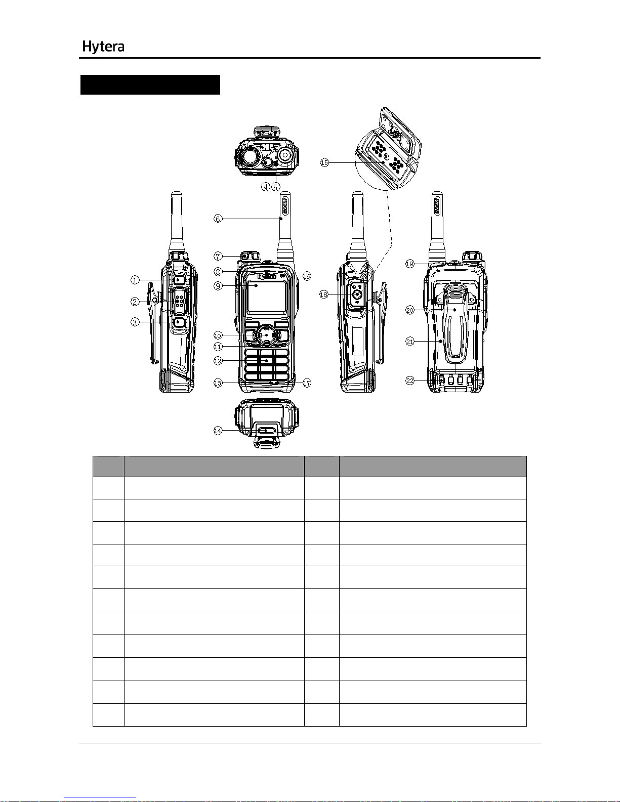
Product Controls
No. Part Name No. Part Name
○
1
SK1 (programmable)
○
2
PTT Key
○
3
SK2 (programmable)
○
4
Emergency Key
○
5
LED Indicator
○
6
Antenna
○
7
Multi-function Control Knob
○
8
Receiver
○
9
Display
○
10
Function Keypad
○
11
Speaker
○
12
Numeric Keypad
○
13
Light Sensor
○
14
Battery Latch
○
15
Duplex Microphone
○
16
Simplex Microphone
○
17
Accessory Jack Cover
○
18
Accessory Jack
○
19
Strap Hole
○
20
Belt Clip
○
21
Battery
○
22
Charging Piece
3
Service Manual
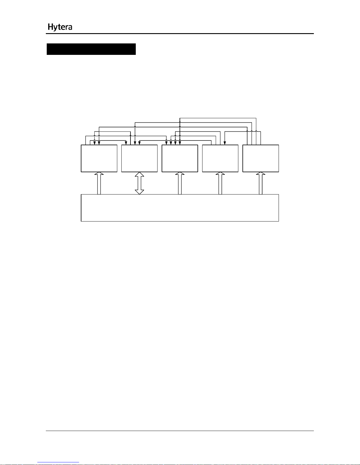
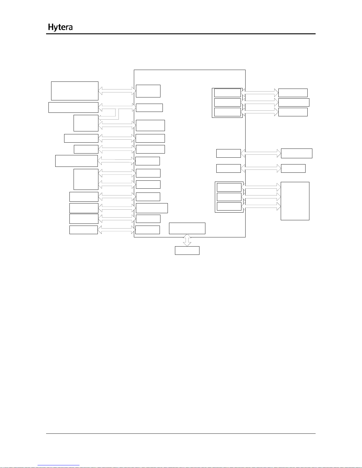
Circuit Description
1. RF Section
The frequency range for PT580 F5 is 806~870MHz (in TMO mode, the frequency range for TX is
806~825MHz, while the frequency range for RX is 851~870MHz; in DMO mode, the frequency range for
both TX and RX is 851~870MHz). The block diagram for the RF section is shown below.
PA
Cartesian
Loop ASIC
RX FGU
POWER_RF
BB TOP
Figure 1 Diagram of RF Section
The RF section consists of PA module, Cartesian Loop ASIC module, RX module, FGU and power
supply module (POWER_RF).
1.1 TX Circuit
4
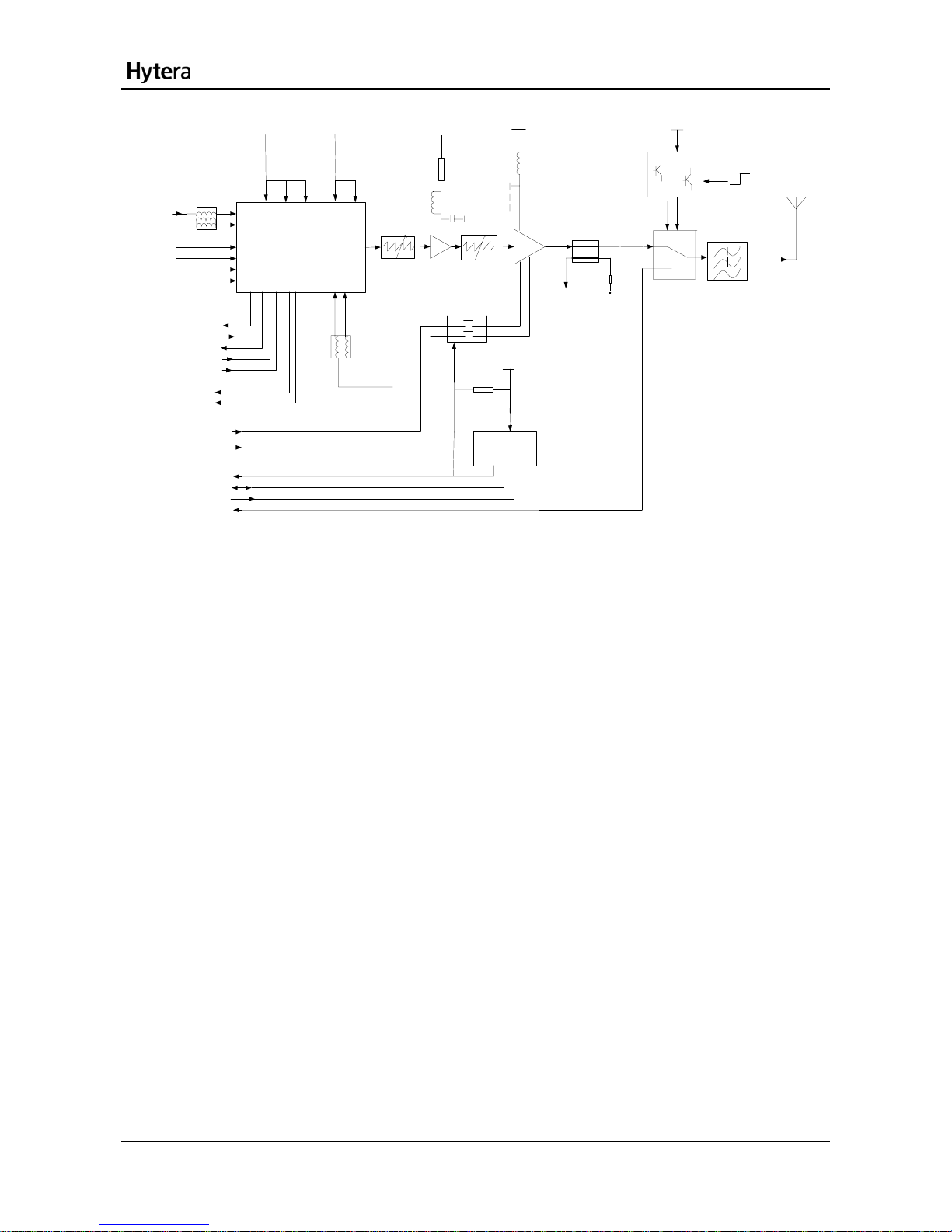
Service Manual
Ca rtesia n IC
DCMEAS
RF_SCLK
RF_DIN
RF_DOUT
TxI+
TxITxQ+
TxQ-
Tx_LO
3V_Tx
RF_SW
7V5
Antenna
PA
3V6_RF
3V_A
Temp erature
Sensor
RF_ F B
TMP_ALERT
SDA
SCL
RX
PA_BIAS1
PA_BIAS2
3V_TxA
3V_TxD
attenu at o r
CSN
DOI
DOQ
RF_ F B
Figure 2 Diagram of TX Circuit
The TX circuit consists of PA, harmonic filter, pre-amplifier, duplexer, coupler, temperature sensor,
TX/RX switch, antenna and etc. The working principle of the TX circuit is described below:
The TX circuit sends the I/Q signal from the baseband section to the Cartesian IC, which outputs
800MHz TX signal after appropriate processing. The TX signal goes to the filter and then to the PA circuit
for amplification after it is converted by BALUN.
The PA circuit is to amplify the RF signal output by the Cartesian IC to obtain an appropriate power level.
Then the signal passes through the TX/RX switch and is sent out from the antenna.
The feedback channel is to couple the power output by the main PA to the Cartesian IC, to form a
complete Cartesian loop. In this way, the output power can be controlled via the attenuation of the
feedback loop.
The temperature sensor will give protection signal if the PA temperature is too high. In such case, the
output power of the PA will be decreased appropriately to prevent damage to the parts.
The signal output by the main PA passes through the TX/RX switch and then goes to the antenna. The
TX/RX switch controls the TX/RX status according to the control signal output by the baseband.
The interfaces between the TX circuit and the baseband or other circuits are described below.
(1) TMP_ALERT
This is the alarm output interface of the temperature sensor, and is connected with the baseband. It
5

Service Manual
6
outputs low level during normal operation, and outputs high level to notify the baseband to reduce the PA
power if the temperature exceeds the preset level.
(2) PA_BIAS1 (same as PA_BIAS2)
This interface is used by the baseband to set the bias status of the PA. In TX status, the level is 2.47V.
(3) RF_SW
This interface is used to transfer the TX/RX switch signal output by the baseband. In the case of high
level, the antenna switch is connected to the output end of the PA, and the RF signal output by the PA is
sent to the antenna via the antenna switch. In the case of low level, the receiver is on, while the
transmitter is off. The antenna switch is connected to the RX interface.
(4) RX
This interface sends the signal to the RX module when the RF_SW switches to the RX end.
(5) RF_FB
This interface feeds the coupled signal back to the Cartesian IC to control the output power.
(6) Tx I+/- and Tx Q+/-
These interfaces are used to transfer the I/Q differential signals from the modulator. The DC level of the
signals is 1.6V, and Vp-p is 1.3 V.
(7) RF_SCLK/RF_DIN/RF_DOUT/CSN
These interfaces are used to transfer the clock signal, data signal and enable signal from the baseband,
and used by the baseband to program the register.
(8) DCMEAS
This interface is used to transfer the signal sent to the baseband for determining whether the DC
calibration is successful.
(9) TX_LO
The signals generated by the TX 1st LO are sent by the VCO to the Cartesian IC, where they are divided
to TX carrier signals. This interface is used to transfer such TX carrier signals.
1.2 RX Circuit
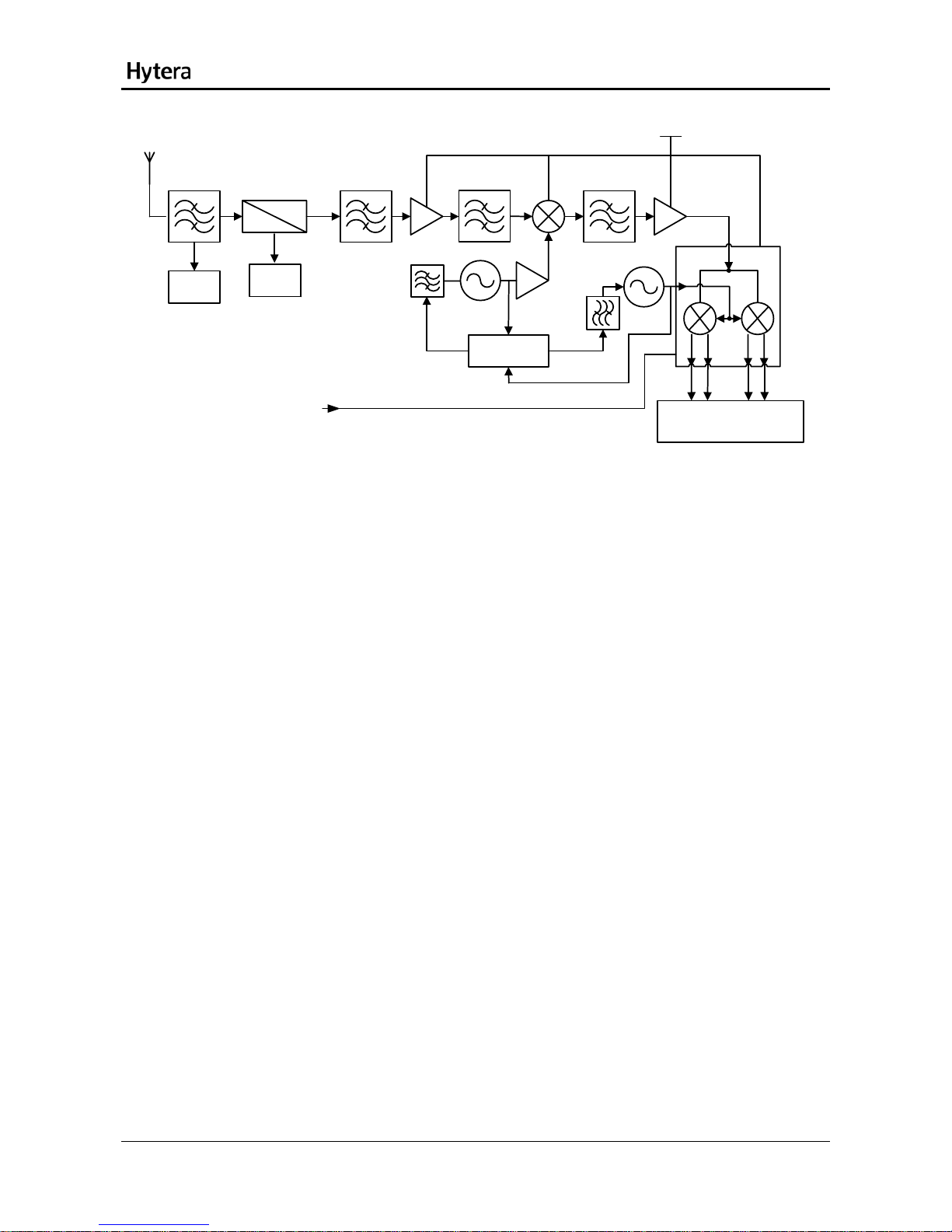
Service Manual
T
R
LNA
IF Amplifier
IF BPF
Mixer
Diplexer
ANT
BPF BPF
Buffer
Demodulator
LPF
LPF
Rx_LO1
Rx_LO2
Rx PLL
IQ Processor
ANT Switch
GPS
TX
3V_Rx
RX I+
RX I-
RX Q+
RX Q-
AGC
RX
Figure 3 Diagram of RX Circuit
The working principle of the RX circuit is described below:
The RX signals pass through the RF switch. First, they are filtered to remove out-of-band signals. Then
they are amplified by the LNA and filtered again. After that, the signals are sent to the mixer for
appropriate processing. The signals output from the mixer are processed by the IF low-noise amplifier
and then by the IF filter to select desired IF signals for demodulation. The obtained I/Q signals are
filtered and finally sent to the baseband for processing.
The interfaces between the RX circuit and the baseband or other circuits are described below.
(1) 3V_RX
This interface is used to transfer the receiver on/off signal from the baseband. If the signal is at high level,
the receiver is on and the RX channel works.
(2) RX
This interface is used to transfer the RX signal output by the antenna switch of the PA.
(3) RX_LO1
This interface is used to transfer the first RX LO signal output by the VCO.
(4) RX_LO2
This interface is used to transfer the second RX LO signal (level: -10dBm) output by the VCO. The signal
enters the IF demodulator, where it is divided and then demodulated together with the first RX IF signal.
(5) AGC
The AGC control voltage from the baseband enters via this interface, to stabilize output of the I/Q
7
Service Manual
demodulator. The AGC voltage varies within 0.2V~1.2V. When the AGC control voltage is 0.2V, the gain
gets to its maximum value.
(6) Rx I+/ - and Rx Q+/-
These interface are used to transfer the differential I/Q signals output by the I/Q demodulator.
1.3 FGU
a1
1
a2
2
3
a3
4
a4
b1
b2
b3
b4
5
6
7
8
Vcc 1
0
GND
0
PLL IC
12MHz _REF
SYN_ON
SYN_CS
SYNTH _LOCK
Loop Filter RxVCO 2
CPout IF
LOOP Filter TXVCO & RXVCO1
CPout RF
5V_SYN
FLout IF
FLout RF
FinIF
FinRF
Figure 4 Diagram of FGU
The working principle of the FGU is described below:
The reference frequency output by the baseband enters the PLL for frequency division. Meanwhile, the
frequency generated by the VCO goes to the divider for frequency division. Then the signals resulted
from both frequency divisions are sent to the phase detector for phase detection. If the signals have
different frequencies or phases, the phase detector will output a signal corresponding to the phase
difference. The signal goes to the low-pass filter to remove high-order harmonics, so as to control the
oscillation frequency of the VCO.
The interfaces between the FGU and the baseband are described below:
(1) FinRF
This interface is used to transfer the feedback signal from the TX/RX VCO to the PLL.
(2) FinIF
This interface is used to transfer the feedback signal from the RX IF VCO to the PLL.
(3) CPout RF
This interface is used to transfer the charging voltage signal from the PLL to the TX/RX VCO.
(4) CPout IF
8
Service Manual
This interface is used to transfer the charging voltage signal from the PLL to the RX IF VCO.
(5) FLout IF
This interface is used to transfer the charging voltage lock signal from the PLL to the RX IF VCO.
(6) FLout RF
This interface is used to transfer the charging voltage lock signal from the PLL to the TX/RX VCO.
(7) SYNTH_LOCK
This interface is used to transfer the PLL lock indication signal to the baseband. When this pin outputs
high level signal, it indicates the PLL is locked.
(8) SYN_ON
This interface is used to transfer the PLL enable signal from the baseband. It outputs 3.3V voltage, and
is open in normal status.
(9) 12MHz_REF
This interface is used to transfer the reference frequency for the PLL.
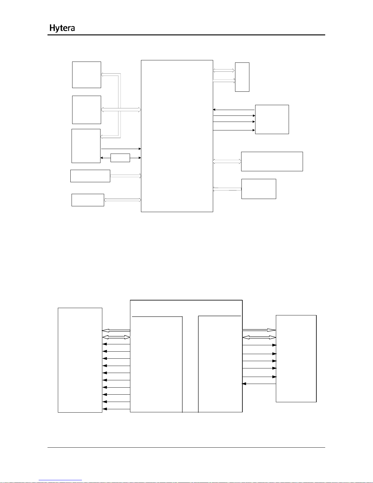
1.4 VCO
VCO VCO
BP filter
BUFFERBUFFER
TRIPLE
5V SYN _ON
TX LO
RX LO
RVO SWITCH
TVO SWITCH
RX LO OUTPUT
TX LO OUTPUT
Figure 5 Diagram of VCO
The working principle of the VCO is described below:
The PLL outputs the control voltage CV. When the RX VCO is locked, it will be output to the receiver via
the BUFFER. When the TX VCO is locked, it will be output to the receiver via the BUFFER, TRIPLE and
filter. The VCO that is powered up will be locked.
The interfaces between the VCO and the baseband or other circuits are described below.
(1) CV: This interface is used by the PLL to output control voltage.
(2) RVO SWITCH: This interface is used to supply power to the RX VCO.
9
Service Manual
(3) TVO SWITCH: This interface is used to supply power to the TX VCO.
(4) RX LO OUTPUT: This interface is used by the RX LO to output signal to the RX mixer.
(5) TX LO OUTPUT: This interface is used by the TX LO to output signal to the Cartesian IC.
1.5 Power Supply Module
3V3D
60R
3V3_RF
LDO
Rx_ON
RF LNA
MIXER
IF LN A
Demodulator
3V_RX
80mA
LDO
Tx_ON
Modulator
3V_TX
140mA
LDO
Modulator
PLL IC
LT5509
3V_A
9mA
SYN_ON
LDO
3V_B
100uA
SYN_ON
Tx_ON
Rx_VCO _ON
TX_ L O _B uffe r
TX_Drive
3V_TX DR V
LO1_Drive
RX LO2_VCO
3V_RVC O
V_PA
60R
DC/DC
LDO
5V_SYN
RX_VCO_ON
Tx_VCO _ON
RX LO1 VCO
5V_RVC O
TX LO VCO
5V_TVC O
Figure 6 Diagram of Power Supply Module
This module is to supply appropriate voltages to the RF circuits. The 3V3D voltage is supplied by the
power management IC of the baseband section, and passes through different LDOs to supply the
10
Service Manual
Cartesian IC, TX VCO, RX VCO, pre-amplifier and other RX parts respectively. The V_PA is supplied by
the battery directly. The SYN control signal is open while the portable terminal is operating.
2. Baseband Section
2.1 Power Section
BATTERY
Farad Battery
Z
Z
ON/OFF
V_PA
VBAT
1V8D
1V6D
2V5D
3V_TXCO
3V3D
3.3V_RF
LDO
1V2D
TO RF PART
TO RF PART
PMU
U6001
Figure 7 Diagram of Power Section
The 3V3D, 1V6D, 1V8D and 3V_TXCO are the necessary voltages for the MCU to start up. The MCU
may not start if any of the four voltages becomes invalid.
The 3V3D, 2V5D, 1V2D and 3V_TXCO are the necessary voltages for the FPGA to start up. The FPGA
may not start if any of the four voltages becomes invalid.
No. Network Test Point
Reference Voltage during Start-up (V)
(while running Bootloader)
Reference Voltage
after Start-up (V)
1 VBAT L6004_2
3.6~4.2 3.6~4.2
2 3V3D TP6001 3.3 3.15
3 1V8D TP6002 1.8 1.8
4 1V6D TP6003 1.6 1.35
5 2V5D TP6004 2.5 2.5
6 3V_TXCO TP6005 3 3
7 1V2D TP6006 1.2 1.2
11
Service Manual
2.2 Control Section
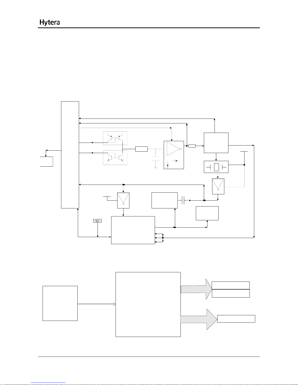
2.2.1 MCU
CAMERA
LCD(WITH
CONTROL
)
GPIO
16 bit EMIFS
16 bit EMIFF
JTAG
32.768 KHz and
12 MHz CLOCK
MCU(ARM+DSP
)
UART 1
UART 3
UART 2
MCBSP3
MCBSP2
MCBSP1
I2C
MMC/ SD CARD
MPUIO
5* 5 KEY
PWL
SPI
8 bit
Reserve
5*5
25 KEY
EMLUATOR
CLOCK
CONTROL
LED and GPIO
LCD and KEY
BACKLED CONTROL
LED
128 Mbit SDRAM
16 bit
128Mbit FLASH
16 bit
16 bit
PIXEL≤160 * 128
,
COLOR=262K
RF and LCD etc.
RF etc.
CMD1
CMD2
TX/RX
CHANNEL
CODEC
CONTROL
FPGA
FLASH.CS and
GPIO
Reserve
Baseband
Processor
PC
Reserve
Reserve
LCD
Figure 8 Diagram of MCU
The dual-core (ARM+DSP) MCU (main frequency speed of 144MHz) accommodates multiple peripheral
interfaces to directly control the LED, LCD, keys and etc. The serial interfaces contain I
2
C, SPI, MCBSP
and MCSI.
12
Service Manual
2.2.2 FPGA
FPGA
MCU
CODER SWITCH
LCD
SIM CARD
SIM _RST
SIM_CLK
SIM_DATA
SIM_SUPPLY
9. 2 16 M _ F PG A
9.216MHz
9.216M_VCO_ON
/VCO_UP
VCO_D OW N
12MHz
BB
.
PROCESSOR
/RST_OUT
/RS T.OUT
RF
MANOUTX
MANOUTY
Acceleration
Sensor
MEMORY
MCBSP2. FSX
CMX_ IRQ2
CMX_ BITCLK
SYMCLOCK
SPI
CONTRAL
I/O
CLK
EMIFS
Figure 9 Diagram of FPGA
The FPGA is mainly for channel control, volume control, sequence control, clock management, IO
expansion control, encryption algorithm and etc.
2.2.3 Memory
The MCU provides two types of external memory interfaces: external memory interface slow (EMIFS)
and external memory interface fast (EMIFF).
MCU U2001
EMIFF EMIFS
SDRAM.A[0:12]
FLASH.A[24:1]
SDRAM.D[0:15] FLASH.A[15:0]
SDR AM.BA0
SDR AM.BA1
SDRAM.CAS#
FLASH.CS3#
SDR AM.RAS#
RST_OUT#
SDRAM.CKE#
SDRAM.CLK#
SDRAM.CS#
SDRAM.WE#
SDRAM.DQML
SDRAM.DQMU
A[0:12]
D[0:15]
BA0
BA1
CAS#
RAS#
CKE
CLK
CS#
WE#
LDQM
ULQM
FLASH U2003
A[23:0]
DQ[15:0]
OE#
WE#
Cef#
RESET#
WP#/ACC
RY/Byf#
FLAS H.WP #
FLAS H.RD Y
FLASH.OE#
FLASH.WE#
SDRAM U2004
Figure 10 Diagram of Memory
13
Service Manual
The MCU is connected with a 128Mbits NOR FLASH (for program or data storage) and a 128Mbits
SDRAM (for temporary data storage).
2.2.4 CLOCK
The 32K clock, also called real-time clock (RTC), is used for system starting, timing, sleeping and etc.
The generation of the 9.216MHz clock is controlled by the FPGA. This clock is provided to the baseband
processor.
FPGA
R
9.216_VCO_ON
/VCO_UP
VCO_DOWN
MCLK
DA
+3V_TCXO
12MHz_REF
PLL
OSCINIF
RF
12MHz
AFC
Synthesizer
12MHz_CLK
CPU
OSC1_IN
OSC1.IN
1V6D
32.768K
12MHz_CLK
9.216M_FPGA
SIM
SIM_CLK
Cartesian
Loop IC
SCLK
BITCLK
SPI.SCK
MCBSP1_CLKX
MCBSP2_CLKX
MCBSP3 _CLKX
9.216M_CLK
CLK32_K
IN
CLK
32K
_
SYMCLOCK
CMX_SCLK
SPI.SCK
SCK
CLK
RF
Baseband
Processor
IO
_L02P
_1/A14
R
Figure 11 Diagram of CLOCK
2.2.5 Reset signal
NOR Flash
PMU
/RESET
/RST-OUT
LCD
CODEC
MCU
RESET-CODEC
/RST-OUT
Figure 12 Diagram of Reset Signal
14
Service Manual
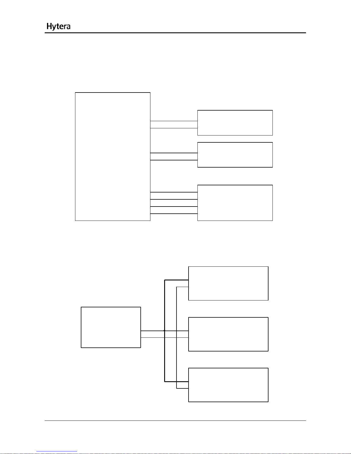
2.2.6 UART
The MCU has 3 UART interfaces: UART1, UART2 and UART 3. The communication rate can be up to
1.5Mbps. The UART connection is shown in Figure 13. The UART2 interface is connected to the
accessory jack for upgrading and programming, while the UART1 and UART3 interfaces are reserved.
UART_RXD
UART_TXD
UART_RTS
UART_CTS
U2501
PC
Reserve
U2001
UART3.RX
UART3.TX
UART2.RX
UART2.TX
UART1.RX
UART1.TX
MCU
UART3.CTS
UART3.RTS
RXA
TXA
J2502
TXA
RXA
J2501
Reserve
Figure 13 Diagram of UART Connection
2.2.7 I2C
The MCU provides one I
2
C interface for the MCU to control the PMU and RTC.
I2C.SCL
SCL
SDA
PMU
SDA
SCL
RTC
SDA
SCL
Reserve
U2001
I2C.SDA
MCU
Figure 14 Diagram of I
2
C Connection
15
Service Manual
2.3 Audio Section
MCBSP 1
MCBSP 3
MCBSP 2
FSB3
FSB1
FSB2
RF
CLOCK
IRQ
RESET
IRQ
RESET
CLOCK
MIC 1
MIC 2
AUD
EAR
PA
CODEC
MCU
DSP
I/Q
FPGA
b
Baseband
Processor
Figure 15 Diagram of Audio Processing Circuit
2.3.1 Audio input
The audio signal from the MIC goes to the baseband processor for amplification, A/D conversion,
encoding and filtering. After such processing, the PCM code is generated, and is then sent to the MCU
for voice encoding and channel encoding by the DSP. After that, it is converted to I/Q signal by the
baseband processor via π/4 DQPSK modulation, filtering and D/A conversion. Finally, the I/Q signal is
sent via the antenna after modulation, amplification and filtering.
2.3.2 Audio output
The RF signal passes through the antenna, LNA, mixer, filter, IF amplifier and demodulator. After
demodulation, the I/Q signal is sent to the baseband processor for A/D conversion and filtering, and then
enters the MCU via the serial port. After π/4 DQPSK demodulation, channel decoding, voice decoding
by the MCU, the signal is converted to audio signal by the baseband processor via filtering and D/A
conversion. Then the audio signal goes to the audio amplifier. After amplification, the audio can drive the
speaker (the audio can be heard from an earpiece if the analog switch is connected with the accessory
jack). The signal from the receiver (duplex) is output by the baseband processor directly (not passing
through the audio amplifier).
2.3.3 Audio Amplifier Output
Main parameters are listed in the table below:
Rated Power (P
o
) 1W
R L = 4Ω
Maximum Power (P
max
) 1.5W
R
L
= 4Ω
Note: The terminal adopts the class D amplifiers.
16
Service Manual
17
Tuning Description
For details about tuning, please refer to the help file for appropriate tuner software supplied by us.
The test standard for current is described in the table below:
No. Test Item Test Value Test Condition
1 Power-off current Test value≤2mA
2 Mean stand-by current in TMO
(screen off)
140mA≤test value≤170mA
3
Mean stand-by current in DMO
(screen off)
210mA≤test value≤250mA
300mA≤test value≤650mA (the
antenna is connected.)
4
Mean TX current in DMO
(screen off)
300mA≤test value≤650mA (the
50Ω load is connected.)
Test v a l u e ≤1900mA (the antenna
is connected.)
5
Max. TX current in DMO
(screen off)
Test v a l u e ≤1800mA (the 50Ω
load is connected.)
300mA≤test value≤650mA (the
antenna is connected.)
6
Mean TX current in TMO
(screen off)
300mA≤test value≤650mA (the
50Ω load is connected.)
Test v a l u e ≤1900mA (the antenna
is connected.)
7
Max. TX current in TMO
(screen off)
Test v a l u e ≤1800mA (the 50Ω
load is connected.)
The voltage is 3.7V. Test
instrument and software:
Agilent power supply, GPIB
card, computer and current
test software.
Service Manual
18
Interface Definition
The interfaces on the main board contain those for data, keyboard, side key, LED, receiver, MIC,
speaker motor, encoder switch and etc.
J7001: 70-Pin Interface
Pin No. Name Function Valid Level
69, 70 GND Power supply: ground (analog) L
4
5
UP_MIC+
UP_MIC-
Upper MIC interface -
6
7
LOW-MIC-
LOW-MIC+
Lower MIC interface -
12
13
14
15
16
17
18
19
20
21
22
23
24
25
26
27
D0
D1
D2
D3
D4
D5
D6
D7
D8
D9
D10
D11
D12
D13
D14
D15
LCD data cable -
34, 35 3V3D Power supply: 3.3V H
9
11
USB-D+
USB-D-
Reserved -
Service Manual
19
Pin No. Name Function Valid Level
47 ALARM Alarm signal L
32, 33 VBAT Battery voltage H
1 RECEIVER Receiver signal -
53
54
LED1
LED2
LED control signal H
65
64
63
62
61
KB-R0
KB-R1
KB-R2
KB-R3
KB-R4
Keyboard row L
60
59
58
57
56
KB-C0
KB-C1
KB-C2
KB-C3
KB-C4
Keyboard column -
46 PTT PTT key detection L
43
42
30
OPT_SEL1
OPT_SEL2
OPT_SEL3
Accessory identification -
29
28
UART2.TX
UART2.RX
PC serial port connection -
31
51
52
36
48
USB.PUEN
USB.DP
USB.DM
RTS
CTS
Reserved -
8
9
/OE
/WE
LCD control interface -
Service Manual
20
Pin No. Name Function Valid Level
10
11
50
55
/LCD_CS
A1
LCD_RST
LCD_BACKLIGHT
67
66
I2C-SCL
I2C-SDA
-
49 L_INT
Reserved
-
44
45
AUDIO_PA_ON
INT/EXT AUDIO
Audio control -
37 ON/OFF Power-on/off control H
39
40
41
ENC_S
ENC_A
ENC_B
Encoder switch signal -
68 ACC_DET Reserved -
38 KEY_LIGHT Key light control H
48
50
IN-SPK-
IN-SPK+
Internal speaker -
2
3
SPK-
SPK+
Speaker audio -
J7004: 30-Pin LCD Interface
Pin No. Name Function Valid Level
1
23
26
VSS Ground (digital) -
2-17 LCD-D0----LCD-D15 LCD data -
18 CS LCD chip select L
19 RESET Reset signal -
Service Manual
21
Pin No. Name Function Valid Level
20 RS Data and command -
21 WR Write signal L
22 /OE Read signal L
24
25
3V3D Power supply: 3.3V -
27 LEDA Power supply for backlight -
28
29
30
LEDK1
LEDK2
LEDK3
Backlight control L
J7007: 21-Pin Keyboard Interface
Pin No. Name Function Valid Level
1
4
21
GND Ground (analog & digital) L
2
3
LOW-MIC+
LOW-MIC-
Lower MIC interface -
5
6
16
I2C-SCL
I2C-SDA
L_INT
Reserved -
7
8
9
10
11
KB-C3
KB-C4
KB-C0
KB-C1
KB-C2
Keyboard column -
12
13
14
KB-R1
KB-R2
KB-R3
Keyboard row L
Service Manual
22
Pin No. Name Function Valid Level
15 KB-R4
17 KEY_LED LED control -
18 3V3D 3.3V power supply -
19 VBAT Battery voltage -
20 ON/OFF Power-on/off control H
Service Manual
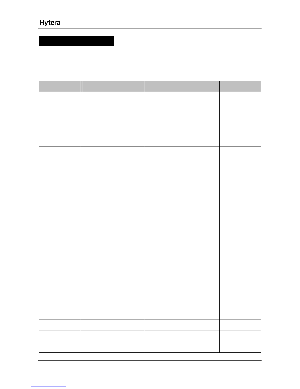
Troubleshooting Flow Chart
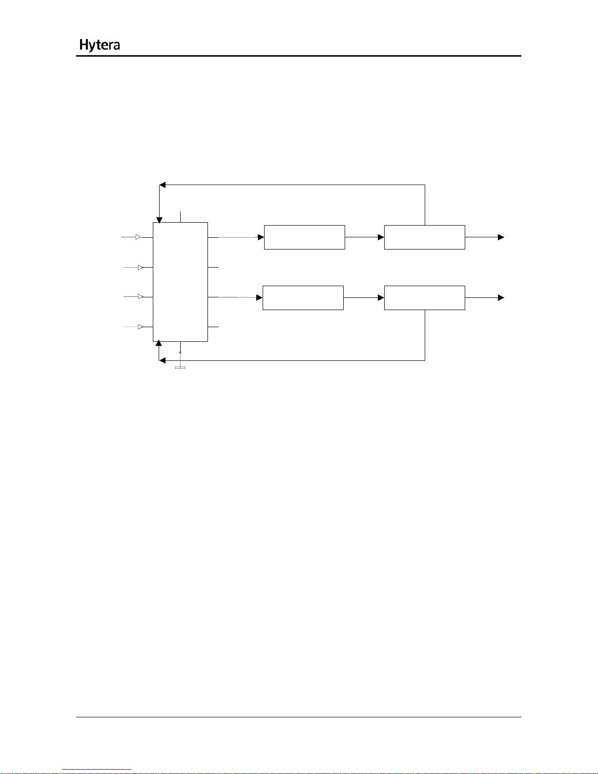
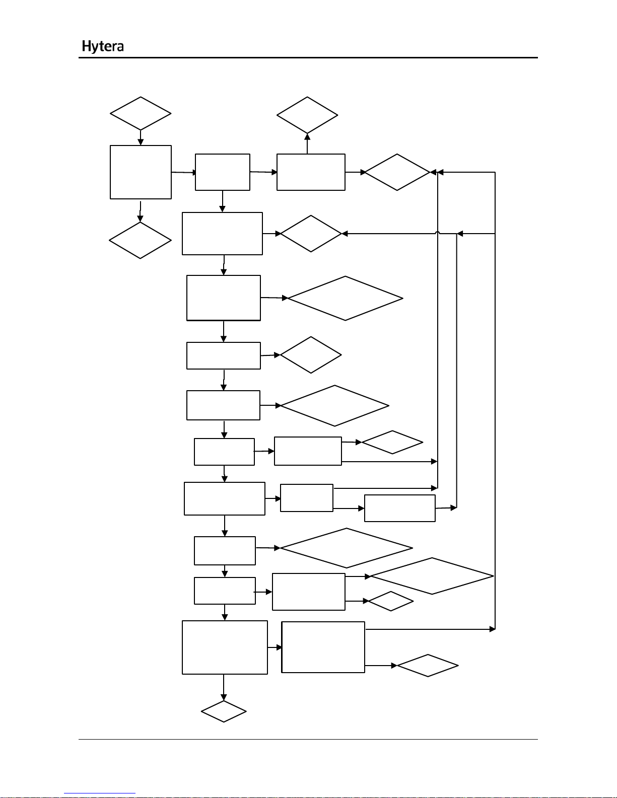
TX Circuit
Yes
Abnormal powe r output
If the current is over
500mA, it indicates
the PA is damaged.
Please replace the
PA (U4102).
Select the test mode and supply 3.7V
voltage. Then check whether the standby
current (240mA) is normal.
No
Yes
Check the TX VCO.
Make the TX VCO locked. Then check
whether the TX VCO outputs stably
[1]
No
Make the TX link in
open-loop working
status.
Check whether the
open-loop transmission
is normal. [2}
Yes
No
Replace
C4139.
Check whether C4139
is soldered inappropriately or
damaged.
Yes
No
Replace the
damaged
parts.
Check whether R4010\
R4011\R4015\C3013\C4014
is soldered inappropriately or
damaged.
Yes
No
Replace the
feedback
balun.
Check whether T4002 is soldered
inappropriately or damaged.
No
Yes
Check whether U4002 outputs
normally. [ 6]
No
Yes
Replace U4002.
Check whether
U4001 outputs normally. [7]
No
Yes
Check whether
T4001 and the
filter are
soldered
inappropriately
or damaged.
Check whether the input I/Q signal for
U4001 is normal. [8]
Yes
Check the
baseband.
Completed
Check whether the s pring
plate for the antenna is assembled
properly. [3]
Check whether U4103 is normal. [4]
Check whether U4102 is supplied
normally. [ 5]
Re-assemble the
spring plate or
replace it.
Replace U4103.
Replace U4102.
Yes
No
No
No
No
Yes
Yes
Yes
23

Service Manual
24
Description:
[1] The lock range for the TX VCO is 1612~1740MHz, and the output amplitude is over -15dBm.
[2] The output power is 27~30dBm during normal open-loop transmission.
[3] The spring plate is flexible and is securely connected with the antenna connector.
[4] When U4103 is normal, Pin4=6.5V, Pin6=0V
[5] When U4102 is supplied normally, Pin15/Pin16=2.8V, Pin9/Pin10/Pin11/Pin12=3.7V, Pout=28~
31dBm.
[6] When U4002 outputs normally, Pin6=3.0V, Pout=about 0dBm.
[7] U4001 outputs 806~870MHz Tetra signal and the amplitude is about -15~-5dBm.
[8] I/Q signal input at Pin20/Pin61: Detect the I/Q signal via an oscilloscope. In normal situation, it is the
modulation signal loaded on the 1.6V DC voltage, and its Vp-p is above 50mV.
Service Manual
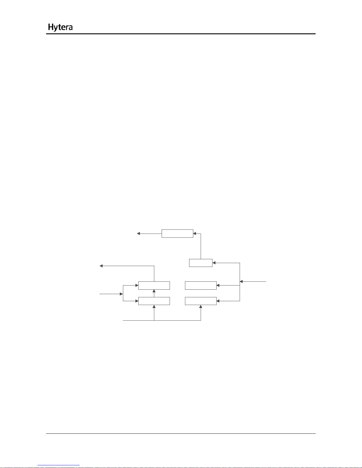
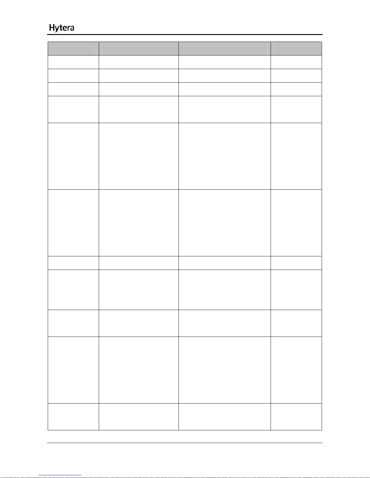
RX Circuit
Abnormal reception
Test TP5001 and
TP5002 to check
whether the I/Q signal is
normal. [12]
Yes
Check whether
I/Q signal is output
via the baseband.
No
Check the power
supply for the receiver
and whether U6501
outputs 3V voltage.
No
Check whether 3.3V input
voltage is available at Pin1
of U6501 and 3.3V enable
signal is available at Pin3.
No
Yes
Check the
enable signal and
power supply via the
baseband.
Replace U6501.
Yes
Check whether the RF LO and IF
LO of the receiver work normally
and whether normal stable
voltage is available at L1001 and
L1004. [1]
No
Check the FGU.
Yes
Check whether the amplitude
of the signal at Pin5 of U4103
is normal. [2]
No
Check whether the antenna
connector or duplexer is inappropriately
soldered or damaged.
Yes
Check whether the amplitude
of the signal at Pin1 of U410 is
normal. [3]
No
Replace U4103.
Yes
Check whether the amplitude
of the input signal at Pin1 of
U5001 is normal. [4]
No
Check whether Z5001/D5001
/C5001 is inappropriately soldered or
damaged.
Yes
Check whether the
amplitude of the output
signal at U5001 is
normal. [5]
No
No
Check whether Pin3/Pin4
of U5001 is supplied
normally. [6]
Replace U5001.
Yes
Yes
Check whether U5002 outputs
73.35MHz IF signal. [7]
No
Check whether Pin4
of U5002 is supplied
normally. [8]
No
Yes
Check whether normal RF
LO signal is available at Pin3
of U5002. [13]
Yes
Check whether the
amplitude of the output
signal at Z5003 is
normal. [9 ]
No
Check the Z5003 match circuit to see
whether Z5003 is soldered inappropriately. If
not, please replace Z5003.
Yes
Check whether the
amplitude of the output
signal at Q5001 is
normal. [10 ]
No
Check whether the voltage for
Pin2/Pin3 of Q5001 is normal.
[11]
No
Yes
Check whether the 3.3V RX voltage is
normal. If yes, please replace U5003.
Replace
Q5001.
Yes
Test TP5001 and TP5002 to check
whether normal I/Q signal is
availablel. [12]
No
Check whether 3V voltage is
supplied to Pin2/Pin20 of U5005,
and whether 146.7MHz IF LO
signal is available at Pin1/Pin28.
No
Yes
Replace U5005.
Yes
Completed
25

Service Manual
26
Description:
[1] The I/Q signals detected by the oscilloscope are modulation signals above 100mV.
[2] Apply -40dBm dot-frequency signal at the RF antenna connector (the -40dBm dot-frequency signal
will be applied at the antenna connector for the following signal amplitude detections unless
otherwise specified), and the amplitude of the signal at Pin5 of U4103 is -40~-50dBm when the
receiver is working.
[3] If the signal amplitude is normal, Pin4=0.3V, Pin6=3.3V.
[4] The normal amplitude range is -40~-55dBm.
[5] The amplitude of the output signal at U5001 should be larger than that of the input signal. The
normal range is -30~-40dBm.
[6] The normal voltage for U5001 is 3V.
[7] U5002 outputs 73.35MHz signal. The normal amplitude range is -50~-65dBm.
[8] The normal voltage for U5002 is 3V.
[9] Z5003 is the IF filter. The insertion loss should be less than 4dB, and the amplitude of the output
signal is -50~-70dBm.
[10] The amplitude of the output signal at Q5001 (IF amplifier) is -40~-55dBm, and should be larger than
that at Z5003.
[11] The normal voltage for Q5001 is 3V.
[12] Apply -40dBm Tetra signal at the antenna connector, and check whether I/Q signal is available at
TP5001 and TP5002 via an oscilloscope.
[13] The normal amplitude range is -10~0dBm.
Service Manual
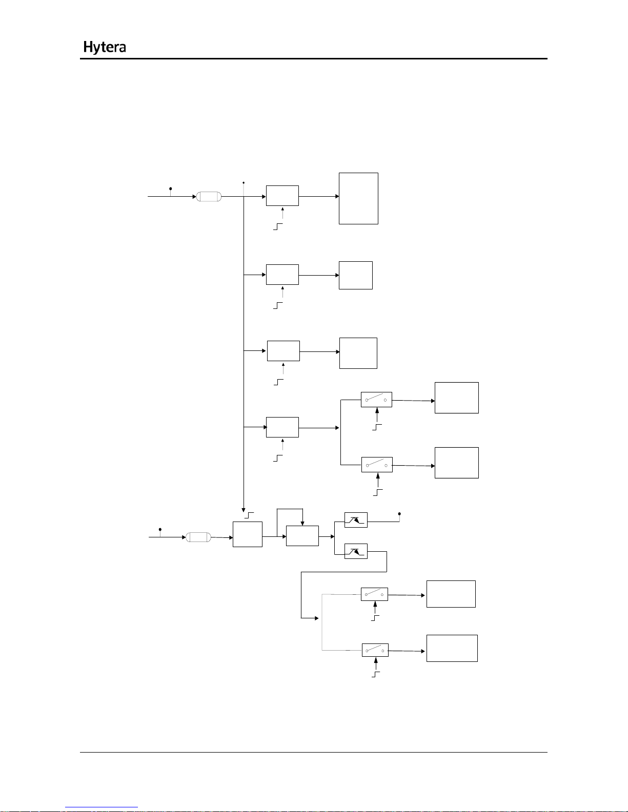
FGU Circuit
CP voltage for TX/RX LO [1]
Check whether
Q6503 is normal . [2]
Check whether
Q6504 is normal . [8]
Check Q6502 and
Q6504.
Check whether
Q1004 is normal.
[4]
Check whether
Q1003 is normal . [4]
Check the varactor. [3]
Check whether
Q1002 is normal. [7]
Check whether
Q1001 is normal. [7]
Check the varactor. [6]
Abnormal FGU
Check whether
Q6502 is normal. [5]
Check U1001. [ 12]
Check whether
Q1007 is normal. [11]
Check whether
Q1006 is normal. [11]
Check whether
Q1005 is normal. [10]
Check the varactor. [9]
Replace the varactor .
Replace Q1005.
Replace Q1006.
Replace Q1007.
Replace Q1004.
Replace Q1003.
Replace the varactor .
Replace Q6503 and
Q6506.
Replace Q1002.
Replace Q1001.
Replace the varactor .
Replace Q6504 and
Q6506.
Yes
No
Yes
Yes
Yes
Yes
Yes
Yes
Yes
Yes
Yes
Yes
Yes
No
No
No
No
No
No
No
No
No
No
No
No
Yes
Replace U1001.
No
Description:
[1] The CP voltage is 0.5~4.5V.
[2] The voltage at Pin4 of Q6503/Q6506 is 5V.
[3] The varactor is not damaged.
[4] The output voltage by Q1003/Q1004 is 4.8V.
[5] The voltage at Pin4 of Q6502/Q6504 is 5V.
[6] The varactor is not damaged.
[7] The output voltage by Q1001/Q1002 is 4.8V.
[8] The voltage at Pin4 of Q6504/Q6506 is 5V.
[9] The varactor is not damaged.
[10] For Q1005/Q1006, the voltage at the collector is 4.8V; the voltage at the grid is 1.8V; and the
voltage at the emitter is 1.2V.
[11] For Q1007, the voltage at the collector is 4.5V; the voltage at the grid is 0.3V; and the voltage at the
emitter is 0V.
[12] For U1001, the voltage at Pin1 is 3V (i.e. voltage at the R1002 end); the voltage at Pin2 is 5V (i.e.
voltage at the R1004 end); Pin9 provides 12MHz sine signal (amplitude: 0.8V).
27
Service Manual
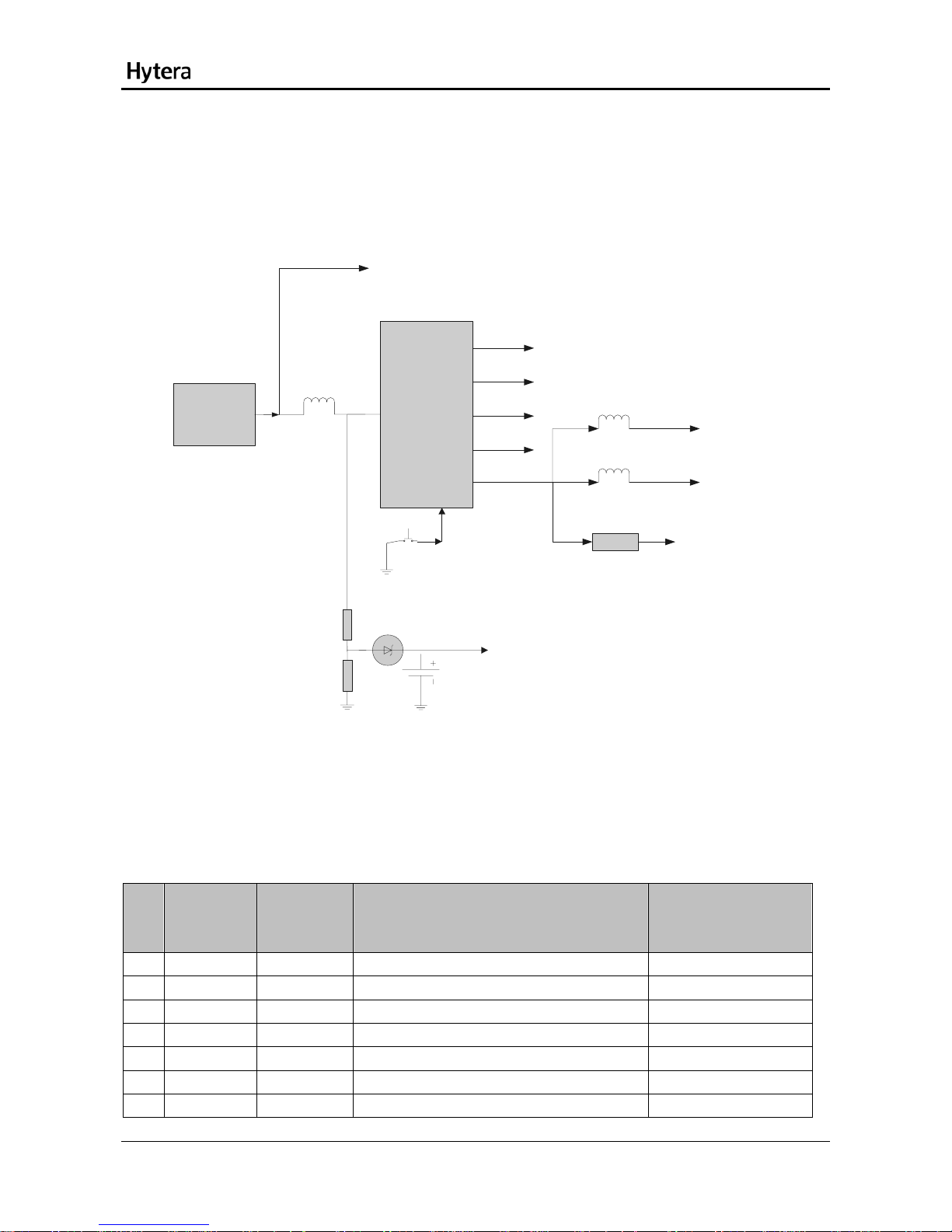
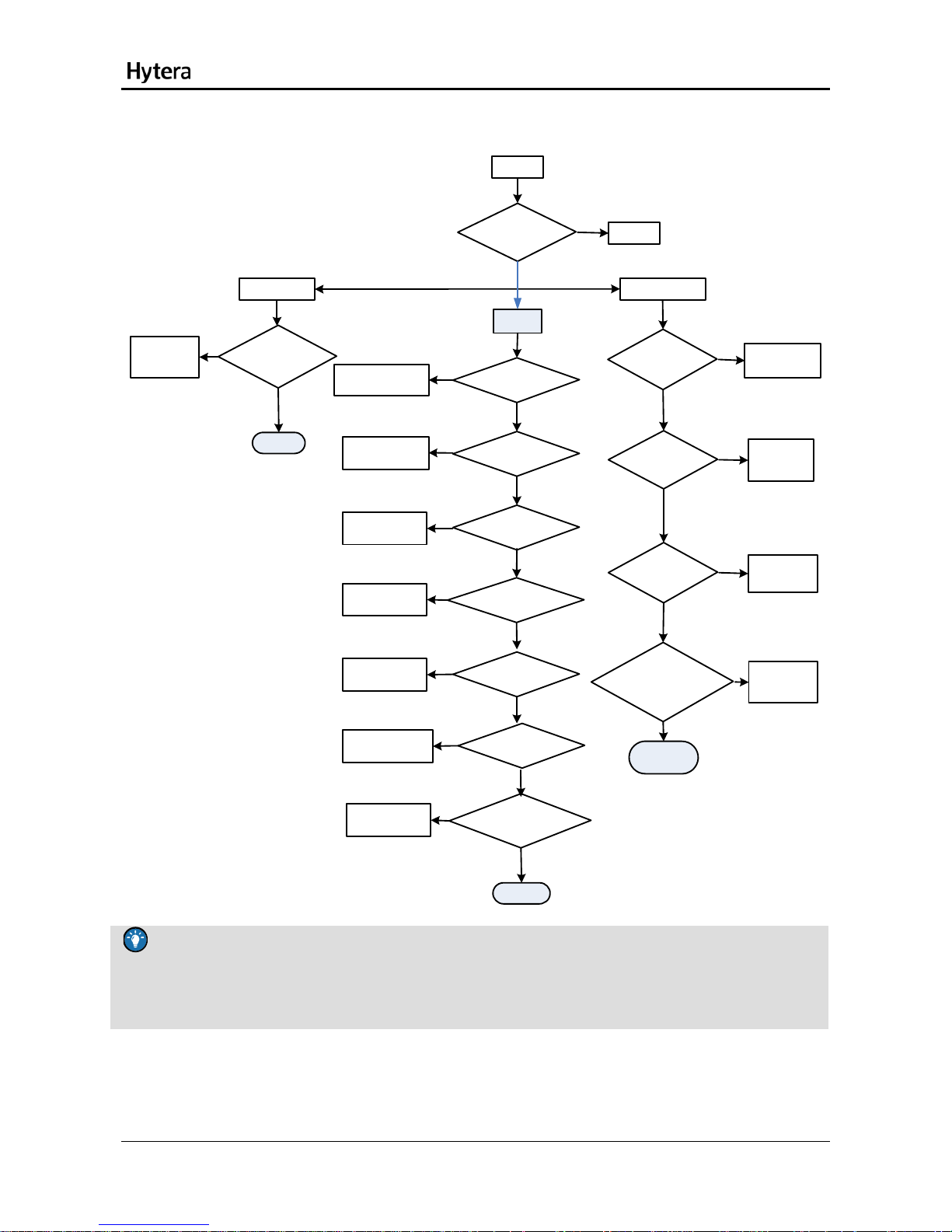
RF POWER Circuit
Abnormal
power
supply
Yes
Check whether
3V3D(TP6001) ou tputs 3.3V
voltage.
No
Check the
baseband.
Yes
Power supply for TX
Power supply for
RX
Check whether
3V_TX is normal. [9]
No
If soldered properl y,
replace U6502.
是
Check whether
3V_A is normal . [10]
No
If soldered
properly, replace
U6503.
Yes
Check whether
3V_RX is normal. [1]
No
Power
supply for
FGU
Yes
Completed
Check whether
3V_B is normal . [11]
No
If soldered
properly, repl ace
U6504.
Yes
Check whether
3V_TXDRV and Q 6501 are normal.
[12]
No
If soldered
properly, replac e
Q6501.
Yes
If soldered
properly, replac e
U6501.
Completed
Check whether U6505 is
normal. [2]
No
If soldered properl y,
replace U6505.
Check whether U6506 is
normal. [3]
If soldered properl y,
replace U6506.
No
Yes
Yes
Check whether Q6505 is
normal. [4]
If soldered properl y,
replace Q6505.
Yes
No
Check whether Q6506 is normal.
[5]
If soldered properl y,
replace Q6506.
No
Yes
Check whether Q6503 is
normal. [7]
If soldered properl y,
replace Q6503.
No
Yes
Check whether Q 6504 is normal.
[8]
If soldered properly,
replace Q6504.
No
Completed
Check whether Q6502 is
normal. [6]
If soldered properl y,
replace Q6502.
No
Yes
Yes
Tip: To check output voltage of U6501/U6502/U6503/U6504/Q6501/Q6502/Q6503/Q6504, the 3.3V
voltage (from the 3.3V control signal of the baseband) is needed at the their enable ends.
28
 Loading...