

Page 1

SERVICE MANUAL
DMR MOBILE RADIO
数 字 车 载 对 讲 机
Page 2

Service Manual
Preface
This manual describes information related with product repair. To repair the product properly, please
read this manual carefully.
This manual is applicable to the following model:
MD78X (X may indicate 2, 5, 6 or 8)
MD78XG (X may indicate 2, 5, 6 or 8)
Note: The description related to GPS is applicable to MD78XG only.
Page 3

Service Manual
Contents
1. RevisionHistory............................................................................................................................................... 1
2. CopyrightInformation......................................................................................................................................2
3. Disclaimer........................................................................................................................................................ 3
4. ProductOverview ............................................................................................................................................ 4
5. ProductControls ..............................................................................................................................................5
6. FrontPanel ...................................................................................................................................................... 7
7. BasebandSection.............................................................................................................................................9
7.1PowerSection .......................................................................................................................................................... 9
7.2PowerOn/Off......................................................................................................................................................... 10
7.3Clock ............................................................................................................................... ........................................ 11
7.4InterfaceDistribution............................................................................................................................... .............. 11
7.5AudioSection ......................................................................................................................................................... 15
7.6PCBDifference ....................................................................................................................................................... 19
8. GPSCircuit..................................................................................................................................................... 20
8.1CircuitDescription.................................................................................................................................................. 20
8.2SchematicDiagram ............................................................................................................................... ................. 20
8.3PartsList ................................................................................................................................................................. 21
8.4TroubleshootingFlowChart ............................................................................................................................... ... 22
9. TuningDescription ......................................................................................................................................... 23
10. InterfaceDefinition .................................................................................................................................... 24
11. UHF1(400‐470MHz25W)Information........................................................................................................ 27
11.1TransmitterCircuit ............................................................................................................................................... 27
11.2ReceiverCircuit ............................................................................................................................... ..................... 29
11.3FrequencyGenerationUnit(FGU) ....................................................................................................................... 30
11.4PCBView.............................................................................................................................................................. 33
11.5BlockDiagram ............................................................................................................................... ....................... 37
11.6SchematicDiagram ............................................................................................................................... ............... 40
11.7PartsList ............................................................................................................................... ................................ 54
i
Page 4

Service Manual
11.8TroubleshootingFlowChart ............................................................................................................................... .89
12. UHF1(400‐470MHz45W)Information........................................................................................................ 95
12.1TransmitterCircuit ............................................................................................................................................... 95
12.2ReceiverCircuit ............................................................................................................................... ..................... 97
12.3FrequencyGenerationUnit(FGU) ....................................................................................................................... 98
12.4PCBView............................................................................................................................................................ 101
12.5BlockDiagram ............................................................................................................................... ..................... 105
12.6SchematicDiagram ............................................................................................................................... ............. 108
12.7PartsList ............................................................................................................................... .............................. 122
12.8TroubleshootingFlowChart .............................................................................................................................. 157
13. UHF2(450‐520MHz25W)Information...................................................................................................... 163
13.1TransmitterCircuit ............................................................................................................................................. 163
13.2ReceiverCircuit ............................................................................................................................... ................... 165
13.3FrequencyGenerationUnit(FGU) ..................................................................................................................... 166
13.4PCBView............................................................................................................................................................ 169
13.5BlockDiagram ............................................................................................................................... ..................... 173
13.6SchematicDiagram ............................................................................................................................... ............. 176
13.7PartsList ............................................................................................................................... .............................. 190
13.8TroubleshootingFlowChart .............................................................................................................................. 226
14. UHF2(450‐520MHz45W)Information...................................................................................................... 232
14.1TransmitterCircuit ............................................................................................................................................. 232
14.2ReceiverCircuit ............................................................................................................................... ................... 234
14.3FrequencyGenerationUnit(FGU) ..................................................................................................................... 235
14.4PCBView............................................................................................................................................................ 238
14.5BlockDiagram ............................................................................................................................... ..................... 242
14.6SchematicDiagram ............................................................................................................................... ............. 245
14.7PartsList ............................................................................................................................... .............................. 259
14.8TroubleshootingFlowChart .............................................................................................................................. 295
15. UHF3(350‐400MHz25W)Information...................................................................................................... 301
15.1TransmitterCircuit ............................................................................................................................................. 301
15.2ReceiverCircuit ............................................................................................................................... ................... 303
15.3FrequencyGenerationUnit(FGU) ..................................................................................................................... 304
ii
Page 5

Service Manual
15.4PCBView............................................................................................................................................................ 307
15.5BlockDiagram ............................................................................................................................... ..................... 311
15.6SchematicDiagram ............................................................................................................................... ............. 314
15.7PartsList ............................................................................................................................... .............................. 328
15.8TroubleshootingFlowChart .............................................................................................................................. 364
16. UHF3(350‐400MHz45W)Information...................................................................................................... 370
16.1TransmitterCircuit ............................................................................................................................................. 370
16.2ReceiverCircuit ............................................................................................................................... ................... 372
16.3FrequencyGenerationUnit(FGU) ..................................................................................................................... 373
16.4PCBView............................................................................................................................................................ 376
16.5BlockDiagram ............................................................................................................................... ..................... 380
16.6SchematicDiagram ............................................................................................................................... ............. 383
16.7PartsList ............................................................................................................................... .............................. 397
16.8TroubleshootingFlowChart .............................................................................................................................. 433
17. VHF(136‐174MHz25W)Information ........................................................................................................ 439
17.1TransmitterCircuit ............................................................................................................................................. 439
17.2ReceiverCircuit .................................................................................................................................................. 441
17.3FrequencyGenerationUnit(FGU) ..................................................................................................................... 442
17.4PCBView ............................................................................................................................................................ 445
17.5BlockDiagram ............................................................................................................................... ..................... 449
17.6SchematicDiagram ............................................................................................................................................ 452
17.7PartsList ............................................................................................................................................................. 466
17.8TroubleshootingFlowChart .............................................................................................................................. 5 03
18. VHF(136‐174MHz50W)Information........................................................................................................ 509
18.1TransmitterCircuit ............................................................................................................................................. 509
18.2ReceiverCircuit ............................................................................................................................... ................... 511
18.3FrequencyGenerationUnit(FGU) ..................................................................................................................... 512
18.4PCBView............................................................................................................................................................ 515
18.5BlockDiagram ............................................................................................................................... ..................... 519
18.6SchematicDiagram ............................................................................................................................... ............. 522
18.7PartsList ............................................................................................................................... .............................. 536
18.8TroubleshootingFlowChart .............................................................................................................................. 573
iii
Page 6

Service Manual
19. DisassemblyandAssembly....................................................................................................................... 579
20. ExplodedView ......................................................................................................................................... 582
21. PackingGuide .......................................................................................................................................... 585
22. Specifications........................................................................................................................................... 586
iv
Page 7

Service Manual
1. Revision History
Version Date Description
R2.0 09-2010 Initial Release
R3.5 05-2011 Add descriptions on VHF, UHF2 and UHF3.
1
Page 8

Service Manual
2. Copyright Information
Hytera is the trademark or registered trademark of Hytera Communications Co., Ltd. (the Company) in
PRC and/or other countries or areas. The Company retains the ownership of its trademarks and product
names. All other trademarks and/or product names that may be used in this manual are properties of
their respective owners.
The product described in this manual may include the Company’s computer programs stored in memory
or other media. Laws in PRC and/or other countries or areas protect the exclusive rights of the Company
with respect to its computer programs. The purchase of this product shall not be deemed to grant, either
directly or by implication, any rights to the purchaser regarding the Company’s computer programs. Any
of the Company’s computer programs may not be copied, modified, distributed, decompiled, or
reverse-engineered in any manner without the prior written consent of the Company.
TM
The AMBE+2
voice coding technology embodied in this product is protected by intellectual property
rights including patent rights, copyrights and trade secrets of Digital Voice Systems, Inc. This voice
coding technology is licensed solely for use within this product. The user of this technology is explicitly
prohibited from attempting to decompile, reverse engineer, or disassemble the Object Code or in any
other way convert the Object Code into a human readable form.
U.S. Patent No: #6,912,495 B2, #6,199,037 B1, #5,870,405, #5,826,222, #5,754,974, #5,701,390,
#5,715,365, #5,649,050, #5,630,011, #5,581,656, #5,517,511, #5,491,772, #5,247,579, #5,226,084 and
#5,195,166.
2
Page 9

Service Manual
3. Disclaimer
The Company endeavors to achieve the accuracy and completeness of this manual, but no warranty of
accuracy or reliability is given. All the specifications and designs are subject to change without notice
due to continuous technology development. No part of this manual may be copied, modified, translated,
or distributed in any manner without the express written permission of us.
If you have any suggestions or would like to learn more details, please visit our website at:
http://www.hytera.com
.
3
Page 10

Service Manual
4. Product Overview
Intended User
This manual is intended for use by qualified technicians only.
4
Page 11

Service Manual
5. Product Controls
Front Panel
No. Part Name No. Part Name
nnel
2
○
4
○
6
○
8
○
10
○
12
○
LED Indicator
OK/Menu Key
Power On/Off Key
Down Key
Programmable Keys
Microphone
Index
Installation
1
○
3
○
5
○
7
○
9
○
11
○
Volume Control / Cha
Selector Knob
LCD Display
Back Key
Up Key
Speaker
Microphone Jack
5
Page 12

Service Manual
Rear Panel
No. Part Name No. Part Name
1
○
3
○
Note: The GPS Antenna Connector is only available for MD78XG.
RF Antenna Connector
Accessory Jack
2
○
4
○
Power Inlet
GPS Antenna Connector
6
Page 13
Service Manual
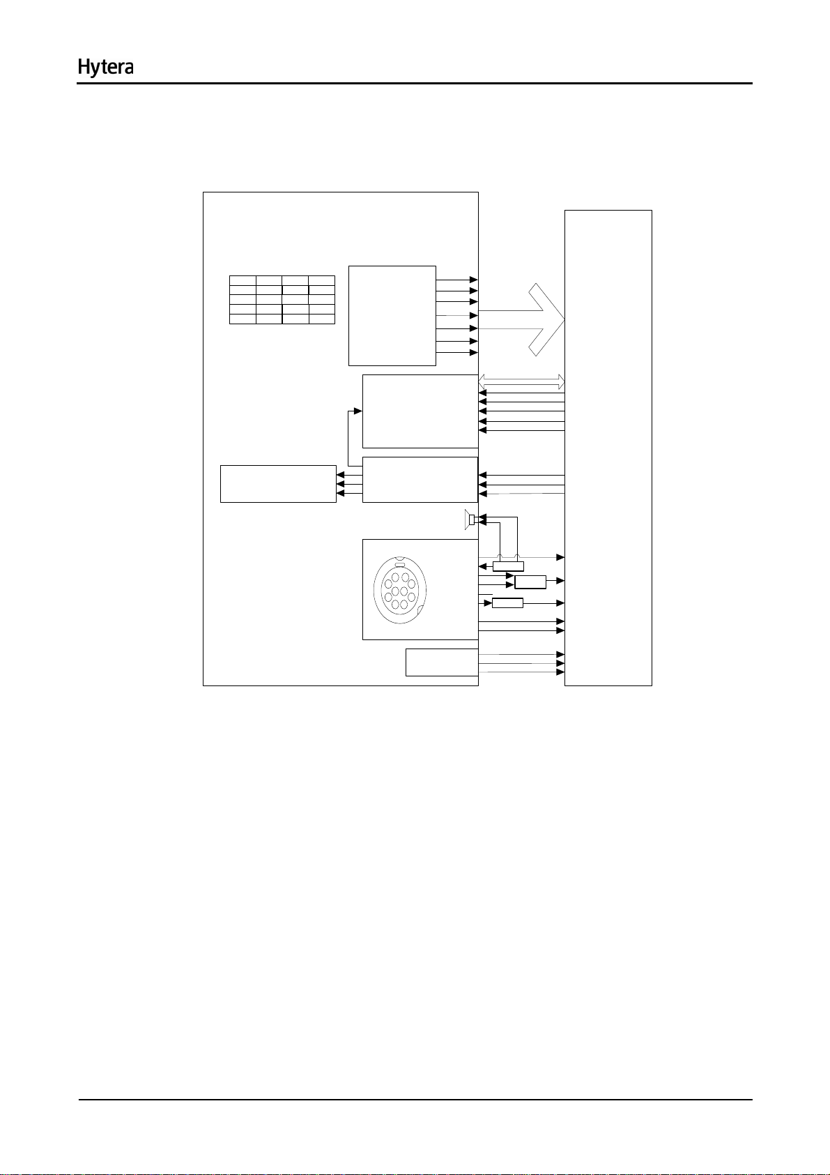
6. Front Panel
The front panel contains the speaker, keys, power switch, volume control knob, LCD display and other
parts. The block diagram is shown as the figure below.
C ON TROL HEAD
Back P2
C0
P6
C1
p1
C2
EMER
C3
BACK LIGHT&
SIGNAL LIGHT
Keys Matr ix
Down
R1R0
R2
P5
SwitchP3
Men u
P4
UP
Keyboard
R1
R2
R3
C1
C2
C3
C4
DB[0:7]
RESET
\CS
\W R
\RD
\RESET
SHIFT_CLK
ACC_ID
GPIO3&PTT
GPIO_2 / DGPIO_1 / D+
USB_Vbus
INT _ MIC
MIC_GROUND
GPIO_4 / Hook
GPIO_0 / PwrO n
SPK
RS
A
5VD
A
B
S
BL_LED
RX_LED
TX_LED
LED
LCD
QA
QB
QC
QD
U1
MMP
U7
Figure 6-1 Diagram of Front Panel
3*4 KEY
U231
U231
EMIFS
SPK+SPK-
FILTER
Keyboard
Interface
FLASH.D
RST_OUT
FLASH.CS2#
FLASH.A1
FLASH.WE#
FLASH.OE#
CS
CLOCK
DATA
GPIO
USB.DP
USB.DM
McBSP
GPIO
GPIO
UART2
GPIO
U302
1) Power Supply
The main board supplies power to the front panel via U902, so that the LED, backlight and USB devices
can be powered up. Then the power is further fed to U5, so as to supply LCD and U1 (serial-to-parallel
converter IC).
2) Keys
The front panel has ten keys: programmable keys (S2, S3, S7, S8, S9, S10 and S12), Up/Down key (S5,
S11), OK/Menu key (S4), Back key (S6), and Power On/Off key (S1).
The operation of each key is identified by a 3X4 matrix keyboard.
3) LCD Display
The TFT LCD transfers data via the bus EMIFS of U302. The control signals contain write/read enable,
memory chip select, LCD chip select and reset signal, each of which is pulled up by R36, R35, R34, R33
7
Page 14

Service Manual
and R6 respectively. The 5V voltage is converted to 3.3V by U5, in order to supply the LCD module.
4) LEDs and Backlight
The LED enable signal is fed to the serial-to-parallel converter IC, and then is output by U302. RX status
is indicated by green LED, and TX status by red LED. Backlight is activated upon key press.
The LEDs (red and green) in series are supplied by a 5V voltage (U902) and controlled by Q2 and Q3.
The backlight is also supplied by a 5V voltage and controlled by Q1. Control signals are output via U1.
5) MMC
For details, please refer to Interface Definition.
6) Audio output
The front panel provides two audio outputs: Handset_audio and SPK±. Handset_audio is the output of
received audio via MMC, and SPK± is the output by the audio PA (U201) as audio signal for the front
panel speaker.
7) Volume Control
The volume control is facilitated by the encoder switch (U7), which generates signals to be fed to U302
by GPIO17 and GPIO18.
8
Page 15

Service Manual
7. Baseband Section
7.1 Power Section
Figure 7-1 Diagram of Power Distribution
Both the baseband control IC and the RF section can convert the supplied voltage to an appropriate one
via the voltage converter.
Supply for RF: U914, Q920 and Q921 supply power for the RF section by high current PNP
transistor and comparator, which can work as LDO (Low Dropout Regulator).
Supply for FGU: U918 and U915 supply 3.3V and 5V respectively to U100.
Supply for Baseband: The processor U302 is supplied by 3.3V (U900), 1.8V (U903) and 1.6V
(U919); the memory is supplied by 3.3V (U900) and 1.8V (U903) respectively; the audio processor
IC is supplied by 3.3V (U900&U909) and 1.8V (U903); the DAC is supplied by 5V (U905) and 3.3V
(U900).
EXT_SWB+: Q909.
9
Page 16

Service Manual
7.2 Power On/Off
The mobile radio can be powered on/off through any of the following methods:
1) Power On/Off key
2) Ignition Signal
3) Emergency
7.2.1 Power On/Off Key
Power on the radio: As the Power On/Off Key is pressed, R944 becomes grounded and Q910 is on.
Then Q905 outputs high-level signal, causing U902 and Q920 to start working. Afterwards the processor
U302 executes user routines to maintain a high-level power control signal (PWR_CTR). In this case, the
radio starts to work properly after the Power On/Off Key is released. Power off the radio: As the Power
On/Off Key is pressed, LQ910 is on and a low-level signal (PWB) to turn off the radio is detected by
U302, which then controls PWR_CTRL to output low level. Afterwards, the radio becomes off.
7.2.2 Ignition Signal
When the voltage of ignition signal exceeds 7V, Q1 will be turned on by C933, R955 and R956. As a
result, the PNP transistor of Q905 will be further turned on to supply power. Meanwhile, Q401 will also be
turned on, and U302 will identify ignition signals by detecting the signal from Q401; afterwards, the level
PWR_CTRL is generated by the processor.
7.2.3 Emergency
When the emergency alarm pin is at low level, R940 is grounded, and Q906 is turned on to supply power.
Meanwhile, Q908 is also turned on. When low level is detected from Q908 but the radio is powered off,
U302 will output the level PWR_CTRL and send emergency signal. If the radio is powered on then, U302
will only output emergency signal.
7.2.4 Power-up Sequence
1) Power on the radio using one of the three methods (Power On/Off key, Ignition Signal, or
Emergency);
2) U917 generates reset signal and remains low level for 1.25 seconds, allowing the processor to
start;
3) Power-on signal will be sent to the processor;
4) After receiving the signal, the processor generates the level of PWR_CTRL. Then the power-up
10
Page 17

Service Manual
procedures are completed.
7.3 Clock
Figure 7-2 Diagram of Clock Distribution
7.3.1 Input Clock
The 32K clock provided by X375 is mainly used for timing and sleeping of the system. Its frequency
(32.768 kHz) is divided by U302 (32768 times in all) to 1Hz for counting seconds. The system clock
(19.2MHz) is generated by an external crystal oscillator.
7.3.2 Output Clock
The baseband outputs 3 clock signals fed to U231, U100 and Option Board respectively.
7.4 Interface Distribution
7.4.1 Serial Peripheral Interface (SPI)
U302
SPIF.CS2PE
SPIF.SCK
SPIF.DOUT
U701
PC
PD
Figure 7-3 Diagram of SPI Interface
SPI of U302 operates in Master Mode, and is controlled by MPU or DMA. In this case, U302 can provide
4 chip select signals, of which CS2 is used to control the IF processor U701.
7.4.2 MCSI Interface
11
Page 18

Service Manual
Figure 7-4 Diagram of MCSI Interface
When U302 is communicating with U100, it works in Master Mode with clock frequency of up to 9.6MHz.
U100 uses MCSI synchronization as chip select signal and MCSI1.DOUT as data cable to configure its
register.
7.4.3 MICROWIRE Interface
Figure 7-5 Diagram of MICROWIRE Interface
The MICROWIRE interface can accommodate 4 external devices at most, generally transmitting control
and status messages of external devices, and reading data from ROM. Its maximum clock frequency is a
quarter of system clock frequency. In this case, MICROWIRE is used to configure or read from the audio
processor. It requires chip select signal CS3.
7.4.4 Serial Synchronous Interface (SSI)
12
Page 19

Service Manual
Figure 7-6 Diagram of SSI Interface
U302 has a total of three McBSP interfaces: McBSP1, McBSP2 and McBSP3, compatible with various
interfaces. McBSP1 is connected with I2C of the audio processor, to realize two-way transmission of
digital voice and data. McBSP2 uses independent clock and frame synchronization for transmitting and
receiving. The SSI of the receiver processor is connected with the RX end of McBSP2, and U500 with
the TX end of McBSP2. U302 works in Master Mode. McBSP3 is connected with the Option Board
interface for both voice and data transmission.
7.4.5 USB Interface
Figure 7-7 Diagram of USB Interface
The radio has two USB interfaces, which are connected to the same USB signal port of the processor.
REF CLOCK is the reference frequency in specified mode. It should be 12MHz in high rate mode or
1.5MHz in low rate mode.
7.4.6 UART Interface
13
Page 20

Service Manual
Figure 7-8 Diagram of UART Interface
U302 has a total of three UART interfaces, which are utilized to communicate with different external
devices. UART2 is used for communication with front panel and serial port on PC, while UART3 with
Option Board and accessory jack (USB).
7.4.7 Mobile Accessory Connector (MAC)
Mobile accessory connector contains audio interface, programmable I/O port, serial port, USB port,
accessory identifier port and etc, which are applied for further development. For details, please refer for
the section Interface Definition.
7.4.8 Option Board Interface
J400, an option board interface, is used to achieve specific function by connecting with the designated
option board. The definition of each pin is listed as below:
14
Page 21

Pin
No.
1
3
5
7
9
11
13
15
17
Service Manual
I/O
Signal Function
GPIO1
GPIO2
GPIO3
GPIO4
GPIO5
UART-TX
UART-RX
UART-CTS
UART-RTS
GPIO
GPIO
GPIO
GPIO
RESET-OUT
UART
Relative
to
Option
Board
I/O
I/O
I/O
O
O
O
I
I
O
Voltage
(VDD=3.3V)
VIH MIN=0.7VDD
VIL MAX=0. 3VDD
VOH MIN=0.8VDD
VOL
MAX=0.22VDD
Remarks
GPIO5: output
signal of the option
board (reset);
GPIO4 and GPIO5:
uni-directional
output interfaces.
They require their
input resistance is
above or equal to
47KΩ.
UART
2
4
6
8
10
12
14 AGND AGND
16 AF OB TO MB AF I
18 AF MB TO OB AF O
19 DGND DGND
I2C –SDA
I2C -SCL
MCBSP-DR
MCBSP-WCLK
MCBSP-DX
MCBSP-FSX
I2C
MCBSP
I/O
O
I
I/O
O
I/O
80mv (standard
output from the
option board to the
main board)
80mv (standard
output from the
main board to the
option board)
I2C
McBSP:
Multichannel
Buffered Serial Port
MAX:700mV
MAX:700mV
20 3V6 or 5V Power O
15
Power supply:
5.0V
Page 22

Service Manual
7.5 Audio Section
Figure 7-9 Diagram of Audio Section
7.5.1 RX Audio Circuit
U302 sends digital audio to the audio processor codec via the SSI bus of MCBSP1. This bus is
composed of CLKX, FSX, DX and DR. It sends the demodulated PCM audio signal to the codec, and
adjusts the signal to appropriate amplitude according to the volume (RMS should be 80mv when
frequency is 1 KHz and deviation is 3 KHz). Then the codec converts PCM data into analog audio data
via DAC. U231 provides two outputs: SPK1 and SPK2. SPK1 is amplified by U238 and then is fed to the
PA U201, to derive two outputs of received audio, which will be applied to the front panel speaker and
further development interface respectively. SPK2 is amplified and divided into the four paths of signal
HANDSET_AUDIO, RX_AUDIO, PUB_ADDESS1 and PUB_ADDESS2. The first two paths are
amplified by U235, and the last two paths are amplified by U236. Output of HANDSET_AUDIO,
PUB_ADDESS1 and PUB_ADDESS2 are controlled by Q231, Q235 and Q233 respectively.
7.5.2 TX Audio Circuit
The audio processor U231 has two MIC inputs: the internal MIC and external MIC. The internal MIC is
connected to the MICIN_HND of U231, and is combined with AUX1 to provide differential input. After
9.3V is divided by R255 and R264, a bias voltage of about 7V is provided to the front panel MIC. The
16
Page 23

Service Manual
external MIC is connected to the MIC_HED of the codec as a unit-directional input. Both MICs are
controlled by Q232. When the internal MIC is active, EXT_MIC_EN is at low level, bias voltage of
external MIC is disconnected, and the ADC in U231 senses voltage at the MICIN_HND. When the
external MIC is active, EXT_MIC_EN is at high level, Q232 is turned on, bias voltage is connected, and
the ADC in U231 senses only audio data at MICIN_HED.
Audio signals input from the MMP interface or the accessory jack, are fed to the codec (gain of codec is
programmable via the CPS) and then are converted by the ADC into 16-bit PCM digital audio, which will
be fed to U302 via the SSI interface.
When the radio is set to operate in loudspeaker mode, audio signal is generated by the internal MIC, and
then feeds to U231, and finally is output via SPK2. The output audio signal is amplified, and then is
output as the two paths of audio PUB_ADDRESS1 and PUB_ADDRESS2.
17
Page 24

Service Manual
7.5.3 Troubleshooting Flow Chart for Control Circuit
18
Page 25

Service Manual
7.6 PCB Difference
The UHF1 PCB has three versions: D, F and H.
The watchdog circuit (in the figure below) is added in version F.
3V3D
3V3D
1000p
R923 0
C937
C978
0.1u
SENCE
RSET
MR
CT
GND
2
WDO
/RST
WDI
6
VDD
1
MBRM120LT1G
MBRM120LT1G
8
7
6
5
U910
5
3
4
C941
0.15u
R920 0
U906
1
MR
2
VCC
3
GND
PFI4PFO
RESET IC
Figure 7-10 Watchdog Circuit
D913
12
D912
12
R983 0
R932
4.7K
/PRST1
1
/PRST
RST_CTRL
Watchdog circuit
The watchdog circuit is used to prevent the radio from damage due to OMAP malfunction. If the program
works properly, U302 feeds pulse signal (25ms) to the watchdog circuit through RST_CTRL. Otherwise,
this pulse signal will be terminated and delayed for more than 1.6s so that U906 generates the reset
signal to reset OMAP.
Compared with version D & F, the difference in version G lies with the audio amplifier, which applies
TDA7297SA instead of TDA7297D.
19
Page 26

Service Manual
8. GPS Circuit
8.1 Circuit Description
GPS
Antenna
GPS
module
REB-1315LPx
Power
UART
OMAP
LCD
Figure 8-1 Diagram of GPS Circuit
GPS positioning information can be acquired via the programmed GPS key on the front panel. The GPS
function is realized via REB-1315LPx module, which integrates GPS baseband processor circuits.
The GPS signal (1.57542GHz), received via the GPS active antenna (with a built-in LNA), goes to the
GPS module for processing, and then enters U302 via the UART port. Meanwhile, U302 sends control
command to the GPS module and forwards processed GPS information to the LCD.
8.2 Schematic Diagram
Figure 8-2 GPS Schematic Diagram
20
Page 27

Service Manual
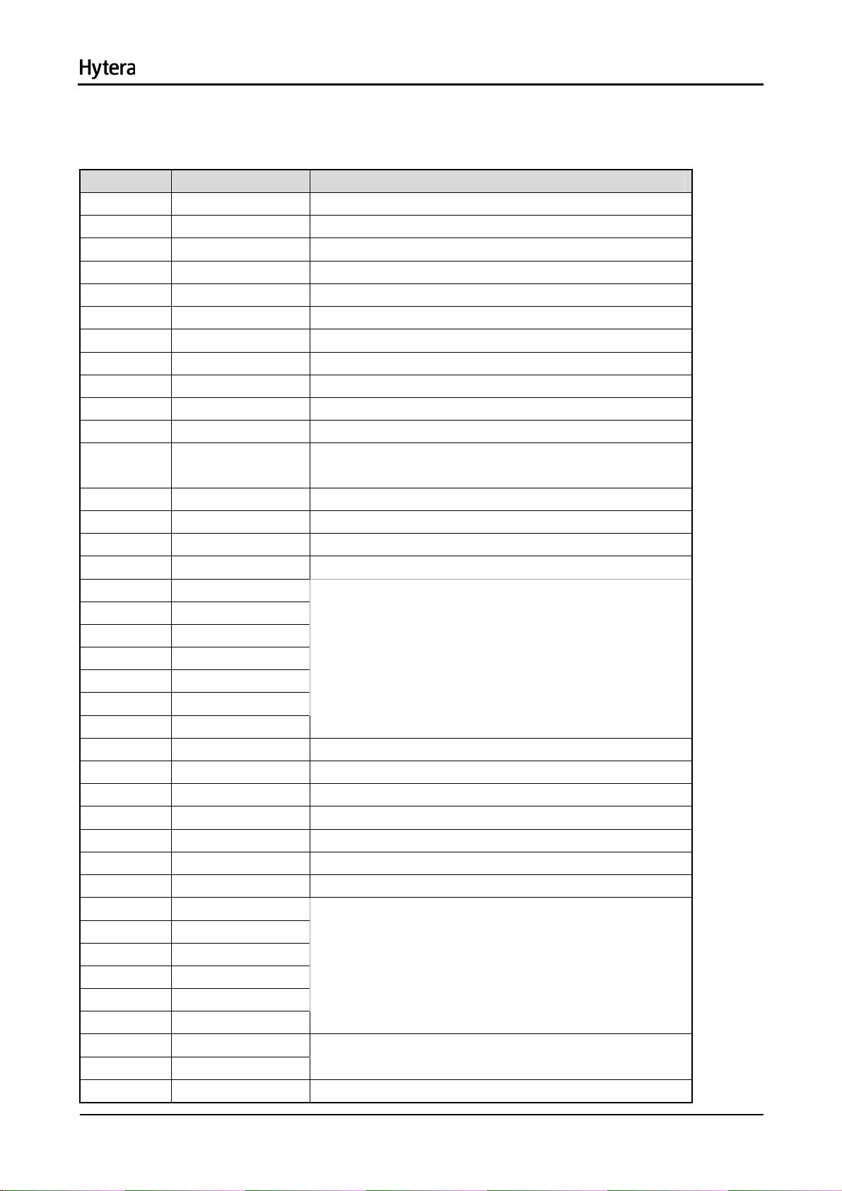
8.3 Parts List
No. Ref.No Part Number Description
1 R348 3001050000000 0Ω
2 R349 3001053300010 33Ω
3 R350 3001053300010 33Ω
4 R365 3001051030000 10KΩ
5 R366 3001051030000 10KΩ
6 C325 3101051040010 0.1UF
7 U326 3625999000030 GPS module
8 W321 4411100002000 IPX RF connector
9 R364 3001050000000 0Ω
10 R363 3001050000000 0Ω
11 L321 3212106390000 39nH
12 C330 3101051040010 0.1UF
13 L322 3221506300000 Ferrite bead
14 C333 3101081060010 10UF
15 C332 3101051040010 0.1UF
16 C331 3101081060010 10UF
17 R418 3001060000000 0Ω
18 R368 3001053300010 33Ω
19 R370 3001053300010 33Ω
21
Page 28
Service Manual
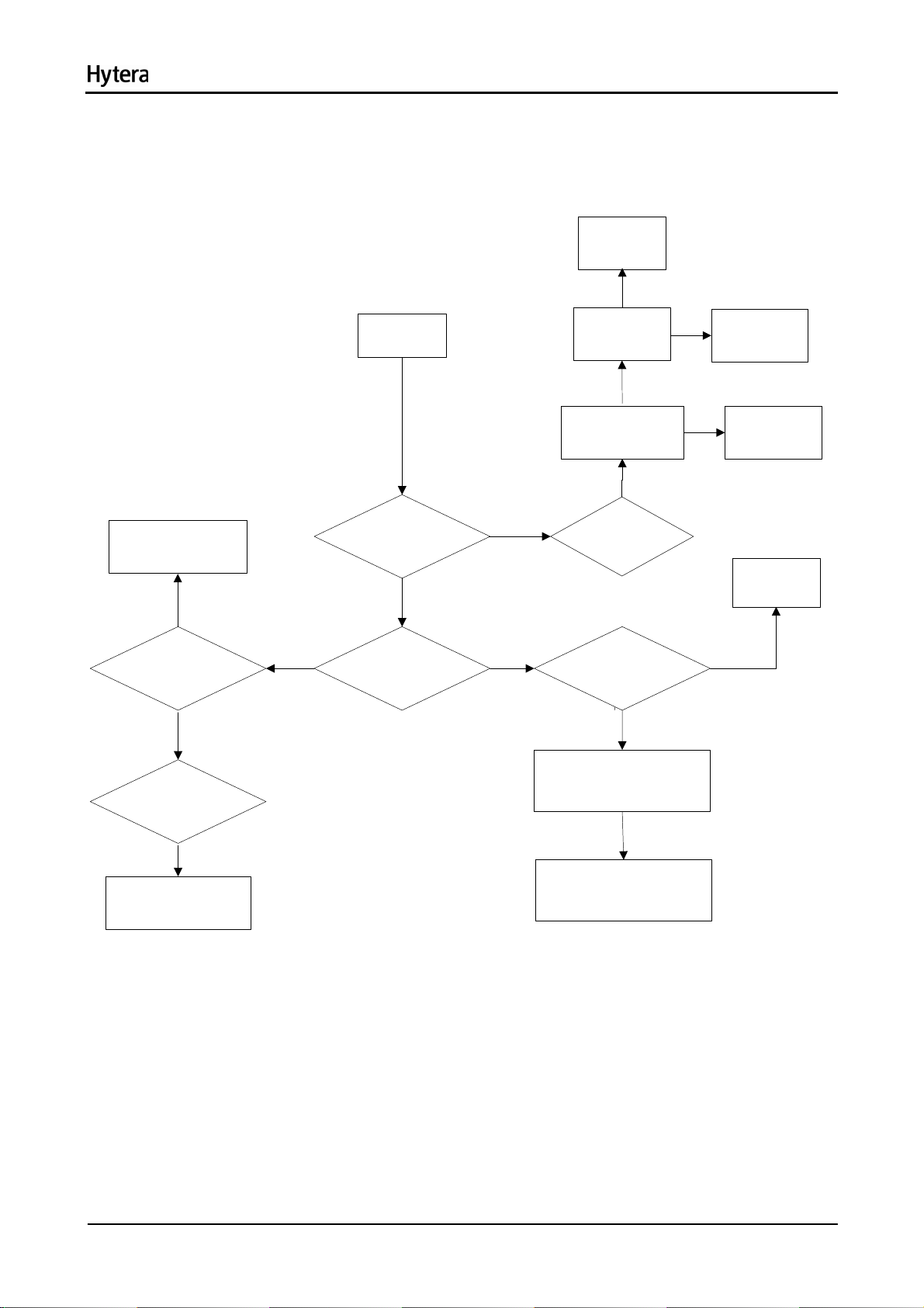
8.4 Troubleshooting Flow Chart
Replace the
GPS
module.
Yes
Replace U901.
No
U901 outputs 3.3V
normally?
Yes
The radio can position
normally?
No
The PC-based
software (e.g.SiRF
Demo) shows GPS
communication?
Start
No
Antenna
works
normally?
Peripheral
components work
normally?
Yes
`
Yes
RX signal is
weak?
Connector works
normally?
Yes
Yes
Yes
No
No
Replace the
antenna.
Replace
defective
components.
Replace
connector
W321.
No
Check UART.
Check R368 and
R370.
Active antenna is
damaged?
Yes
Replace the active
antenna.
22
Page 29

Service Manual
9. Tuning Description
For details about radio tuning, please refer to the help file of DMR Tuner Software supplied by the
Company.
23
Page 30
Service Manual
10. Interface Definition
J404: to front panel jack
Pin No. Name Function
1 INT_MIC Audio input
2 MIC_GROUND Audio input ground
3 ACC_IO1 Accessory identifier pin 1
4 USB_VBUS USB power supply
5 HOOK HOOK
6 PTT PTT
7 USB_D- USB data cable D-
8 USB_D+ USB data cable D+
9 ACC_IO2 Accessory identifier pin 2
10 UART2_RXD_A Volume control port
11 UART2_TXD_B
12
13 SPKR1+ Speaker audio signal cable+
14 SPKR1- Speaker audio signal cable-
15 5VD Power supply
16 PRST Reset signal
17 KB_C0
18 KB_C1
19 KB_C2
20 KB_C3
21 KB_R0
22 KB_R1
23 KB_R2
24 CSLED Backlight control IC chip select
25 CLOCK Backlight control IC clock
26 DATA Backlight control IC data
27 OE_LCD LCD read enable
28 WE_LCD LCD write enable
29 CS2_LCD LCD chip select
30 F_A1_LCD LCD register enable
31 F_D7
32 F_D6
33 F_D5
34 F_D4
35 F_D3
36 F_D2
37 F_D1
38 F_D0
39 GND Ground
HANDSET_AUDI
O
Audio signal output by accessory
Matrix keyboard
LCD data bus
LCD data bus
24
Page 31

Service Manual
40 PWB_IN Power-on/ power-off signal
J4: to aviation jack of front panel
Pin No. Name Function
1 ACC_IO1 Digital input
2 PTT_IN Digital input
3 Handset_Audio Analog output
4 USB_D- USB data cable
5 GND Ground
6 USB_VBUS Power supply
7 MIC_IN Analog input
8 USB_D+ USB data cable
9 HOOK Hook signal input
10 ACC_IO2 Digital input
J2: to LCD display jack
Pin No. Name Function
1 GND Ground
2 VCI 2.5V-3.3V adjustable port
3 VCI 2.5V-3.3V adjustable port
4 IOVCC 1.65V-3.3V adjustable; input/output port
5 FLM Synchronization signal control pin
6 CS Chip select signal
7 RS Register select
8 WR Write signal
9 RD Read signal
10 DB0
11 DB 1
12 DB2
13 DB3
14 DB4
15 DB5
16 DB6
17 DB7
18 DB8
Data bus
19 DB9
20 DB10
21 DB11
22 DB12
23 DB13
24 DB14
25 DB15
26 DB16
27 DB17
25
Page 32

Service Manual
28 RESET Reset signal
29 IM3
Select data cable
30 IM0
31 LEDA LED positive
32 LED_K1
33 LED_K2
LED negative
34 LED_K3
J403: to accessory pin jack
Pin No. Name Function
1 Vbus USB Power supply (+5V)
2 Ground Ground
3 GP5_3 Digital input/output
4 SW B+ sense Power supply
5 External Alarm Analog voltage output
6 Power Ground Power supply ground
7 Tx Audio Analog input
8 RX Audio Analog output
9 Spkr- Analog output
10 D+ USB USB data cable +
11 USB_GROUDN Ground
12 GP5_2 Digital input/output
13 ACC_IO2 Digital input
14 Emerg Sw Digital input
15 ACC_IO3 Digital input
16 PRGM_IN_PTT Digital input
17 Audio Ground Audio ground
18 Spkr+ Analog output
19 D- USB USB data cable -
20 GP5_8 Input/output
21 Ground Ground
22 GP5_7 Input/output
23 GP5_6 Digital input/output
24 AUX Audio Out 1 Analog output
25 AUX Audio Out 2 Analog output
26 Ign Sense Analog voltage input
26
Page 33

Service Manual
11. UHF1 (400-470MHz 25W) Information
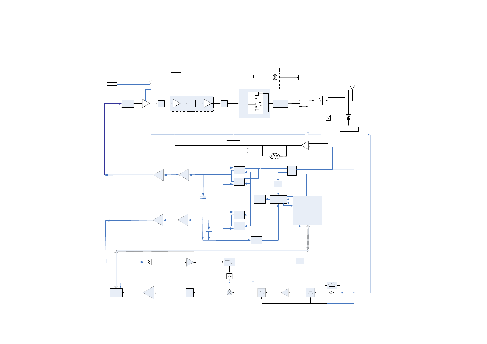
11.1 Transmitter Circuit
The transmitter circuit is composed of power amplifier circuit and power control circuit. The former is
used to amplify the VCO signal to the desired output power level, while the latter can keep the output
power at the desired level, so as to protect the power amplifier from damage caused by over heat,
antenna mismatch, and out-of-range voltage (over voltage or under voltage may result in damage to
Q801, Q805, Q804, Q802 and Q803).
Figure 11-1 Diagram of Transmitter Circuit
11.1.1 Power Amplifier
The 4-stage power amplifier amplifies the signal output from VCO to the required output power level. The
first stage is a buffer amplifier circuit with fixed gain; the second stage is a pre-driver power amplifier
circuit with variable gain (formed by Q805); the third stage is a driver power amplifier circuit with variable
gain (formed by Q804); and the final stage is the final power amplifier circuit with fixed gain (formed by
Q802 and Q803). In addition, this power amplifier contains a TX/RX switch and a low-pass filter.
Note: only a final power amplifier (Q803) is available in later versions (including version H).
11.1.2 TX Buffer Amplifier
The first stage (Q801) provides about 16dB power gain, and adjusts its bias circuit to get a quiescent
bias current of 28mA (for Q801). Power supply for the switching transistor Q810 is controlled by TX
signal (enabled by antenna switch) so as to further control the power supply for the whole circuit.
11.1.3 Pre-driver Power Amplifier
The pre-driver power amplifier is formed by Q805, with variable gain controlled by voltage VGG. The
input matching circuit is composed of C826, L826, L814, C843 and R824.
27
Page 34

Service Manual
11.1.4 Driver Power Amplifier
The driver power amplifier is formed by Q804, with variable gain controlled by voltage VGG. The
maximum output power is 38.5dBm, and the maximum variable gain is 11dB.
11.1.5 Final Power Amplifier
The final power amplifier comprises Q802 and Q803, with the maximum output power of 48.5dBm, and
the maximum variable gain of 10dB. The input matching circuit is composed of C815, C839, R804, R806,
R807, R813, R818 and R861, while the power combining circuit is composed of C820, C8330, C831,
C819, C812, C841 and C842.
1 1.1.6 Antenna Switch
The antenna switch is used to switch between the transmitter circuit and the receiver circuit.
In TX mode, TX signal controls the switching transistor Q810, to further control the power supply 9V 3A
for the PIN diodes D801 and D802. Quiescent bias current of the PIN diode is controlled by the resistors
R821 and R825. In this mode, D801 and D802 are turned on; RF signals are applied to the low-pass
filter (composed of C871, C816, C836, C837, C838, L809, L813, and L810) and then transmitted via the
antenna port.
In RX mode, TX signal controls the switching transistor Q810, to further control the power supply for the
PIN diodes D801 and D802, which are not applied with DC bias current. When the two PIN diodes are
turned off, signals feed into the RX path through the low-pass filter (composed of L871, C852 and C862).
11.1.7 Low-pass Filter
A low-pass filter that consists of inductors L809, L813 and L810, and capacitors C836, C837, C830, is
used to attenuate harmonic energy from the transmitter.
11.1.8 Directional Coupler
A directional coupler that consists of microstrip directional coupler, D803, D804 and etc, is used to detect
both forward and reverse directed power of the transmitter. The forward power is coupled to the diode
D803, and the voltage is applied to the power control circuit (U801). Then the voltage VGG is output to
control the gate voltage of pre-driver and driver PA, ensuring a constant power output.
The directional coupler can adjust the TX power and detect the VSWR load. The reverse power is
coupled to D804. The voltage is applied to U802 and then feeds into U302 for detection
28
Page 35

Service Manual
11.1.9 Output Power Control
The TX power is controlled by U801. The forward power is applied to the directional coupler, to output a
voltage that can represent the forward power. The voltage together with the preset voltage feeds to U801
to output a voltage VGG, which can control both gate voltage and gain of Q804 and Q805, ensuring a
constant power output.
11.1.10 Thermal and Over-voltage Protections
The circuit consists of thermistor RT804 and resistor R884. The output voltage is proportional to the
detected temperature. Both the voltage used for temperature detection and the threshold voltage are fed
into the operational amplifier U803, to output a voltage signal that is in proportion to the detected
temperature. Afterwards, the voltage is applied to software for judgment, and then the preset voltage will
be subsequently changed to reduce the TX power, and to protect the PA from over-heating.
11.1.11 Pressure Pad Switch
The power control circuit includes a pressure pad switch SW1, which is controlled by the conductive
rubber part mounted on the top cover. If the switch is turned off, VGG will become low, and no power will
be output from PA. Otherwise, PA will work normally.
11.2 Receiver Circuit
The receiver utilizes double conversion superheterodyne technique. The first IF is 73.35MHz and the
second IF is 2.25MHz. The first local oscillator signal is from the PLL circuit U100, and the second local
oscillator signal (71.1MHz) from the PLL circuit U701. The major units are BPF, LNA, mixer, IF filter, IF
amplifier and IF processor.
Figure 11-2 Diagram of Receiver Circuit
11.2.1 Receiver Front-end
RF signals feed to the low-pass filter to remove out-of-band signals, and are applied to the two-stage
29
Page 36

Service Manual
electrically tunable band-pass filter to get useful signals. After passing through the RF band-pass filter
and LNA (Q6102), the RF signals together with the first LO signal feed to the mixer for the first frequency
conversion, to generate the first IF signal (73.35MHz). The mixer that employs the passive diode can
ensure good dynamic range and port isolation. The LO signal (3-5dBm) from the VCO feeds to Q6103
to get a gain (17dB). The first LO signals (73.35MHz) pass through the crystal filter (Z6100) to remove
out-of-band spurious signals, and then feed to the two-stage IF amplifier circuit (composed of Q6133 and
Q6134) for amplification. Finally the amplified signals go to the IF IC for processing
11.2.2 Receiver Back-end
Figure 11-3 Diagram of IF Processor
The first IF signal (73.35MHz) output by the IF amplifier goes into IF IC via Pin 47, where the signal is
converted to the second IF signal (2.25MHz). Then the un-demodulated digital I/Q signal output from the
SSI interface is sent to U302 for demodulation. IF IC employs a reference frequency of 19.2MHz and
shares the crystal with U302. The second LO VCO consists of the external transistor, varactor and some
other components, to provide the second LO signal. The 18MHz clock frequency is generated by the LC
resonance loop (D702, L715 and C745).
DSP (U302) gets the audio signal from IF IC (U701). Then this signal goes through U302 to output data
signal, which is sent to U231 and PIN44 (SSI_DI) for digital-to-analog conversion. Finally, the output
analog audio signal will be subjected to gain control, and then fed to the speaker.
11.3 Frequency Generation Unit (FGU)
11.3.1 PLL Synthesizer
30
Page 37

Service Manual
The PLL synthesizer that consists of the reference oscillator (X100), PLL IC (U100) and VCO, is utilized
to supply excitation signal source to the transmitter, and local oscillator signal to the receiver.
11.3.2 Reference Oscillator
X100 is a 19.2MHz TCXO, and its reference frequency is calibrated by the digital-to-analog converter
(U500) for accuracy.
11.3.3 PLL IC
The PLL IC (U100) is a fractional frequency divider. The logic IC U101 and U102 work with the PLL IC
(U100) to achieve locking.
Figure 11-4 Diagram of PLL IC
The 19.2MHz frequency generated by the reference oscillator goes into the PLL IC for division,
generating the reference frequency. Meanwhile, the frequency generated by VCO goes into PLL IC
(U100) for frequency division. The resulting frequency will be compared with the reference frequency in
terms of phase difference in the phase detector. After comparison, the resulting frequency is converted
to CV voltage via the loop filter, to control and lock the frequency.
11.3.4 VCO
The VCO is composed of transistors (Q100, Q103, Q106 and Q110), varactors and four Colpitts
31
Page 38

Service Manual
oscillators. There are four VCOs in all: two VCOs (Q100 and Q103) used to transmit excitation signals
and the other two VCOs (Q106 and Q110) to receive LO signals. U302 controls the operating frequency
of the VCO. Q102 and Q107 constitute the buffer amplifiers for the transmitter circuit, while Q111 and
Q109 for the receiver circuit. The digital-to-analog converter (U500) modulates the TX oscillator signal.
LPF
MOD
PLL IC (U100)
TX PA
RX Lo
Q107
Q109
Q102
Q111
TX_L_VCO
TX_H _VC O
RX_L_V CO
RX_H_VCO
Q103
Q100
Q110
Q106
Figure 11-5 Diagram of VCO
32
Page 39

11.4 PCB View
MD78X/MD78XG PCB View (Front Panel)
Top Layer
33
Page 40

MD78X/MD78XG PCB View (Front Panel)
Bottom Layer
34
Page 41

MD78X/MD78XG PCB View (Main Board)
TopLayer
35
Page 42

MD78X/MD78XG PCB View (Main Board)
Bottom Layer
36
Page 43

11.5 Block Diagram
MD78X/MD78XG Block Diagram (Power Section)
Auto baterry Voltage
13.6f
ON\OFF KEY PWB
IGN_SENCE
EMERGENCY
Q920\Q921\U914
U902
U913
9V3A
5VD
U915
U918
U905
U919
U900
U903
U901
Q802\Q803\U201
Q804\Q805
9V1A
Q801 Q801
9V1A
Q902
U703
U702
Q104
5VA
3V3A
5VA
3V3A
U909
1V6D
1V8D
U302
U233
U910
U231
U232
U302
U326
J400
3V3D
3V3DP
U100
X100
U500
5VA
Q6102
Q6103
U6000
Q6105
U701
U701
4V3A
Q100\Q103\Q106\Q110
U231
X302
U302
U401 USB
Control Head
Accessory Level
Translator
Option board
U912
37
3VRTC
U323
U326
Page 44
MD78X/MD78XG Block Diagram (RF Section)
High
Temperature
Microstrip
Matcher
Temperature
compensation
Protection
Tx/Rx
Switch
Switchÿs Power
9.1V
ADC
Tx_PORT
Rx_PORT
ANT
Microstrip Dual
Harmonic
Directional Coupler
Filter
Forward
Detector
RX
Reflect
Detector
Alarm to ADC
VSWR Protection
TV_APC
9V1A_TX
TXC
Gain:-6 dB
Attenuator
Gain:16 dB
Q801
Firststage
Gain:15 dB
Match
Q805
PreDriver
Gain:11dB
Match
Q804
Driver
Match
Gain:10 dB
Q802ǃQ803
Finalstage
B+
B+
Final_Bias
U701
IF IC
IF Processor
TX LO:3dBm
RX LO:3dBm
1 2
Attenuator
IF Amp
Q6104
Q6105
TX_L_VCO
TX_VCO_L
TX_H_VCO
RX_L_VCO
RX_H_VCO
Q103
TX_VCO_H
Q100
RX_VCO_L
Q110
RX_VCO_H
Q106
VCO_Feed
back LPF
L P F
Q107
Q102
C
Q109
Q111
C
LPF
Q6103
3dB
Z6100
IF Filter
Mixer
D6106
1 2
Attenuator
1dB
Band-pass Filter2
MOD H
MOD L
X100
19.2MHZ
PLL U100
Low-Noise Amp
Q6102
DATA
TV_APC
U500
Final_Bias
DAC
CLK
M C S I
S P I
STB
LD
U302 OMAP
X100
19.2MHZ
Attenuator Control
10dB
Band-pass Filter1
TV
38
Page 45

MD78X/MD78XG Block Diagram (BB Section)
BB Schematic Block Diagram
PLL
IF processor
SSI
SPI
X
R
2
P
S
B
SPI(CS1 )
SPI(CS2)
c
M
DAC
SSI
X
T
_
2
P
S
B
c
M
RF Unit
TXǃRX CTL
PowerǃIO CTL
TEMP_DET
Audio PA
AUX
ADC
Headset
Driver
Mic
AMP
Audio Codec
CP
SPI
Driver
TXAF_DI
RXAF_DO
BOARD/BLUETOOTH
IIS
BELL
CS3
LTR/OPTION
IGN_SENSE
MCLK
EMERGENCY
MCSI1
McBSP1
McBSP3
MCLK19.2MHz
PWM0/
PWT
uWire
UART3
GPIOs
IIC
USB1
SPI
DSP
TMS320C55x
OMAP5912
MPU
ARM926EJ-S
GPIOs
McBSP2
KEY
Trax
GPIOs
UART2
or GPIO
EMIFS
EMIFF
JTAG
CLK
IIC
UART1
GPIOs
datax16
Speed:96MHz(max)
6
x
a
1
t
d
a
32KHz
19.2MHz
TCXO
IGN_SENSE
EMERGENCY
PWB
Nor FLASH and pSRAM
FLASH: 8Mx16
pSRAM:2Mx16
Mobile SDRAM
128Mb:8Mx16
JTAG
19.2MHz
AD9864
RTC
IIC
IIC
User Program
32.768KHz
20ppm
Accelero
meter
GPS
AUX Audio
DC Supply
IGN_SENSE
EMERGENCY
Rear
Accessory(MAP)
PRGM GPIOS
USB
ACC_ID
GPIO
USB
ACC_ID
MIC
SPKr
Control Head
PRGM
GPIOs
MMP
PRGM IO out
GPIO
Expand
light/LED/LCD
TX_RX
backlight
39
74hc595
74hc595
S
C
/
A
T
A
D
/
K
L
C
IO Expand
Keytrax 3X4
LED
UART or
Volume
TFT LCD
ON/OFF KEY
datax8
EMIFS
PWB
Page 46

5
4
3
2
1
11.6 Schematic Diagram
MD78X/MD78XG Schematic Diagram
(Audio Circuit)
R245 1RR245 1R
13
U201
U201
AUDIO PA
AUDIO PA
GND10GND
SGND
NC417NC5
18
R241
R241
120K
120K
C250 220pC250 220p
R248 100KR248 100K
6
5
U235B
U235B
9d3V
34
VAG
C2761uC276
1u
-
-
+
+
4 11
R277
R277
47K
47K
2
OP AMP
OP AMP
6
5
U236B
U236B
R253 1RR253 1R
R293 1RR293 1R
R294 1RR294 1R
R237 120KR237 120K
7
1
UMC4N
UMC4N
Q233
Q233
5
9d3V
OP AMP
OP AMP
9
10
U236C
U236C
-
-
+
+
4 11
9d3V
D D
L232
L232
9V3
BLM18PG300SN1
BLM18PG300SN1
C232
C520
C520
10u/16v
10u/16v
C243
C243
0.1u
0.1u
C256
C256
100P
100P
12
+
+
C232
0.1u
0.1u
3V3A
U237
U237
SWITCH IC
SWITCH IC
VCC5S
2
4
R246 22KR246 22K
C249 1uC249 1u
100K
100K
R296
R296
3 4
2
1
CODEC_/SS
CODEC_SSI_WCLK
CODEC_SSI_BCLK
1
TP232TP232
1
TP233TP233
1
TP234TP234
1
TP235TP235
1
TP236TP236
1V8D
R2300R230
0
C236
C236
0.1u
0.1u
3V3D
R2330R233
0
R234
R234
10K
10K
/CODEC_RST
TP238TP238
C C
TEMP_DET
TEMP_DET2
CODEC_PWT
B B
A A
3V3A
MIC_GROUND
TP4029TP4029
EXT_MIC_EN
R2430R243
0
NEW
INT_MIC
EXT_MIC
TP239TP239
10u/16v
10u/16v
C519
C519
C292
C292
0.01u
0.01u
12
+
+
R25810K R25810K
R261
R261
10K
10K
1
1
R235
R235
10K
10K
R242 0R242 0
C248
C248
0.1u
0.1u
1V8D
C269
C269
220P
220P
C270
C270
220P
220P
C272
C272
220P
220P
9d3V
BB IC
BB IC
R280NC R280NC
R254NC R254NC
R259 10KR259 10K
C260
C260
0.01u
0.01u
C239
C239
0.1u
0.1u
1
2
3
4
5
6
7
8
9
10
11
12
U231
U231
R2490R249
0
C261
C261
0.01u
0.01u
BLM18BD601SN1D
BLM18BD601SN1D
BLM18BD601SN1D
BLM18BD601SN1D
R266 47KR266 47K
RN230
RN230
100*4
100*4
48
49
T-PAD
IOVDD
PWR_DN
RESET
GPIO2
GPIO1
AVDD2
AVSS2
AVDD1
NC9
NC10
NC11
NC12
AVSS113VREF14VBAT15AUX216AUX117BUZZ_IN/CP_INN18CP_OUTP19CP_INP20MICIN_HND21MICBIAS_HND22MICIN_HED23MICBIAS_HED
C2551uC255
1u
R2901K R2901K
C258 0.1uC258 0.1u
L233
L233
BLM18BD601SN1D
BLM18BD601SN1D
L234
L234
L235
L235
R270
R270
47K
47K
DVSS
12
45
47
46
DVDD
OP AMP
OP AMP
2
3
C275
C275
+
+
10uF/16V
10uF/16V
BCLK
678
45
WCLK
44
TP237TP237
C2661uC266
C271
C271
220P
220P
CODEC_SSI_DI
C273
C273
SDIN
R279
R279
1u
220P
220P
CODEC_SSI_DO
123
43
1
30k
30k
C2981uC298
SDOUT
1u
9d3V
CODEC_CLK
CODEC_SCLK
R231 33R231 33
42
41
SCLK
MCLK
C2621uC262
1u
R283
R283
30k
30k
-
-
+
+
U236A
U236A
4 11
/CODEC_DAV
CODEC_MOSI
CODEC_MISO
33
R23233R232
40
37SS38
DAV
MOSI39MISO
DRVSS2
OUT8N
DRVSS1
VGND/CP_OUTN
DRVDD
OUT32N
MIC_DET
24
C2591uC259
1u
R284
R284
R285
R285
15k
15k
C2991uC299
1u
R264 1KR264 1K
R267 1KR267 1K
1
OUT8P
BVDD
SPKFC
SPK2
SPK1
15k
15k
R265
R265
1.8K
1.8K
C295
C295
100P
100P
36
35
34
33
32
31
30
29
28
27
26
25
R236
R236
10K
10K
C2381uC238
1u
RXAF_DO
VAG
3V3A
R2380R238
0
C251 1uC251 1u
R291 0R291 0
R202
R202
10K
10K
C2001uC200
1u
TXAF_DI
C240
C240
0.1u
0.1u
C246NCC246
NC
C267
C267
0.1u
0.1u
B11GND
B03A
R29233R292
VAG
C286
C286
10u/25V
10u/25V
Q234
Q234
UMC4N
UMC4N
C233
C233
0.1u
0.1u
SPK_SEL
VAG
R2876.8KR2876.8K
33
C2911uC291
1u
6
OP AMP
OP AMP
13
12
C257 1uC257 1u
9d3V
R255
R255
470
470
12
+
+
C234
C234
10uF/25V
10uF/25V
12
C289
C289
+
+
0.1u
0.1u
10uF/16V
10uF/16V
C290 1uC290 1u
C247 220pC247 220p
R244 22KR244 22K
-
-
+
+
U235D
U235D
4 11
9d3V
30K
30K
Q232
Q232
3 4
2
1
C279 1uC279 1u
R275
R275
100K
100K
5
R288 47KR288 47K
C245 220pC245 220p
C293
C293
R239 6.8KR239 6.8K
14
UMC4N
UMC4N
B+
B+
V-
V-
4 5
R257
R257
VAG
R273 24KR273 24K
678
-
-
B
B
+
+
A+
A+
C235
C235
0.01u
0.01u
B-
B-
A-
A-
OP AMP
OP AMP
9d3V
C268 0.47uC268 0.47u
9d3V
B OUT
B OUT
C283
C283
V+
V+
0.1u
0.1u
A OUT
A OUT
+
+
A
A
-
-
U238
U238
OP AMP
OP AMP
123
R286 47KR286 47K
C242 220pC242 220p
Q231
Q231
3 4
2
1
UMC4N
UMC4N
C254 220pC254 220p
R252 100KR252 100K
-
-
9
10
5
VAG
+
+
U235C
U235C
9d3V
C274
C274
0.1u
0.1u
C280 220pC280 220p
R274 100KR274 100K
OP AMP
OP AMP
13
12
U236D
U236D
8
4 11
-
-
+
+
4 11
9d3V
B+
12
C284
C284
C285
C285
+
+
2
19
5
16
1
11
20
6
OUT1-
OUT1+
IN1
7
14
C287
C287
0.47u
0.47u
R250 15KR250 15K
R260
R260
C265 220pC265 220p
R262 100KR262 100K
OP AMP
OP AMP
2
3
U235A
U235A
VAG
Q235
Q235
UMC4N
UMC4N
OUT2+
IN2-
9d3V
OUT2-
-
-
+
+
4 11
15
VCC
VCC
MUTE8STBY
9
C294
C294
1uF
1uF
VAG
330mV
R272 47KR272 47K
5
GND
NC13NC2
4
1
R276
R276
100K
100K
12
OP AMP
OP AMP
R269
R269
100K
100K
C2811uC281
1u
GND
NC3
R295 1KR295 1K
47uF/25V
47uF/25V
0.1u
0.1u
R289 0R289 0
C237
C237
0.47u
0.47u
C241 0C241 0
R240 0R240 0
C288
C288
100p
100p
R247
R247
100K
100K
5
C252 1uC252 1u
C2631uC263
1u
14
100
100
C2641uC264
1u
R263
R263
30K
30K
VAG
R268
R268
100K
100K
C2781uC278
1u
3 4
2
1
5
7
-
-
+
+
4 11
C253 1u/25VC253 1u/25V
D230 ESD ICD230 ESD IC
8
UMC4N
UMC4N
C2771uC277
1u
Q230
Q230
TP4012TP4012
C2821uC282
1u
TP4016TP4016
34
2
1
R251
R251
100
100
D231 ESD ICD231 ESD IC
R271
R271
100
100
R278
R278
100
100
LOW_LEVEL_MUTE
600mV
EXT_SPKR+
EXT_SPKRSPKR1+
SPKR1-
9d3V
AUDIO_PA_EN
HANDSET_AUDIO
RX_AUDIO
PUB_ADDRESS2_EN
PUB_ADDRESS2
PUB_ADDRESS1
PUB_ADDRESS1_EN
PUB_ADDRESS_MIC_EN
DESIGNER: LHY
Title
Title
Title
AUDIO
<Title>
<Title>
<Title>
Size Document Number Rev
Size Document Number Rev
Size Document Number Rev
<Doc> <RevCode>
C
<Doc> <RevCode>
C
<Doc> <RevCode>
40
5
4
3
2
C
Date: Sheet of
Date: Sheet of
Date: Sheet
114Monday, November 29, 2010
114Monday, November 29, 2010
114Monday, November 29, 2010
1
of
Page 47

5
4
3
2
1
MD78X/MD78XG Schematic Diagram
(RX Circuit)
L6100
L6100
BLM18PG600SN1
9V1A_RX
1u
R61000R6100
0
3 4
2
1
TP6103
TP6103
TX TP
TX TP
C6118
C6118
470pF
470pF
C6132NCC6132
NC
U6000
U6000
OPAMP
OPAMP
VCC
IN+
VCC
IN+
1
+
+
2
VEE
VEE
-
-
3 4
OUT
IN-
OUT
IN-
TRANSISTOR
TRANSISTOR
Q6100
Q6100
R6106
R6106
680
680
D6100
D6100
HVC131
HVC131
1 2
R6109
R6109
390
390
RX_AFTER
5
5
C6106
C6106
220p
220p
C61096pC6109
12
C6135
C6135
56p
56p
6p
D6101
D6101
1SV279
1SV279
D6102
D6102
1SV279
1SV279
R6111
R6111
100K
100K
C6146
C6146
470P
470P
C61101pC6110
1p
C6136
C6136
56p
56p
C61211pC6121
C6122
C6122
1p
2.2p
2.2p
N3
12
C6137
C6137
47P
47P
C6138
C6138
47P
47P
C61230C6123
0
N4
3
1
L6105
L6105
Micr-L
Micr-L
1 2
D6105
D6105
HSM88AS
HSM88AS
C6119
C6119
C61201pC6120
L6104
L6104
1.5p
1.5p
3
N2
1 2
R6127
R6127
10K
10K
TUHF_TONE
R61400R6140
0
1p
C6134
C6134
56p
56p
Micr-L
Micr-L
N1
R61230R6123
0
TP6110
TP6110
RX CV
RX CV
R611433R6114
33
R6113
R6113
270K
270K
L6101
L6101
BLM18PG600SN1
BLM18PG600SN1
12
C6103
C6103
RX_in
C61451uC6145
1u
C61001uC6100
220p
220p
C6194
C6194
10NH
10NH
D D
RF_ATTEN
L6114
L6114
BLM18PG600SN1
BLM18PG600SN1
TV_APC
9V1A_RX
R61160R6116
0
12
C6144
C6144
220p
220p
C C
BLM18PG600SN1
12
R6101
R6101
C6185
C6185
C6102
C6102
470p
470p
TRANSISTOR
TRANSISTOR
C6104
C6104
0.1u
0.1u
C61126pC6112
C61116pC6111
6p
6p
N17
N18
12
Micr-L
Micr-L
Micr-L
Micr-L
2
3
L6214
L6214
C61334pC6133
L6215
L6215
4p
Q6101
Q6101
680
680
1uF
1uF
1
2
3 456
R6103
R6103
27K
27K
TP6104TP6104
N19
12
C6129
C6129
18p
18p
C6107
C6107
220p
220p
L6110
L6110
15n
15n
C6130
C6130
100p
100p
L6102
L6102
220n
220n
R6105
R6105
5.6K
5.6K
R6110
R6110
1.2K
1.2K
R6107
R6107
1.2k
1.2k
C6113
C6113
0.1u
0.1u
2
R610210R6102
10
L6103
L6103
10n
10n
1
Q6102
Q6102
TRANSISTOR
TRANSISTOR
3
4
R6104
R6104
2.7K
2.7K
C61145pC6114
5p
C6105
C6105
220p
220p
TP6102TP6102
C61150C6115
C6131NCC6131
NC
TX TP
TX TP
TP6101
C6245ncC6245
nc
C6128
C6128
470p
470p
TP6101
C6108
C6108
1000p
1000p
R6108
R6108
4.7K
4.7K
RX_ONE
TP6100
TP6100
GND
GND
1
C61261pC6126
C6125NCC6125
L6106
L6106
Micr-L
Micr-L
N6
0
N5N5
3
1 2
C61166pC6116
1p
NC
6p
12
D6103
D6103
1SV279
1SV279
C6140
C6140
C6139
C6139
56p
56p
56p
56p
C61171pC6117
R6112
R6112
100K
100K
1p
D6104
D6104
1SV279
1SV279
C6147
C6147
0.01u
0.01u
C6141
C6141
56p
56p
C6127
C6127
C61241pC6124
L6107
C6143
C6143
47P
47P
L6107
1p
N7
Micr-R
Micr-R
L6217
L6217
220p
220p
3
1 2
C62466pC6246
6p
C6244ncC6244
nc
L6216
L6216
220p
220p
1.5p
1.5p
12
C6142
C6142
47P
47P
R6115
R6115
100K
100K
L6115
R6125
R6125
820
820
L6115
1 2
BLM18PG600SN1
BLM18PG600SN1
C6193
C6193
0.1u
0.1u
L6121
L6121
BLM18PG600SN1
BLM18PG600SN1
C6182NCC6182
NC
L6127NCL6127
NC
C6148
C6148
470p
470p
C6150NCC6150
NC
C61580C6158
0
12
L6122
L6122
0.1uF
0.1uF
C6174NCC6174
C61491uC6149
1u
C6190
C6190
1uF
1uF
NC
R6118
R6118
3.3K
3.3K
R6129
R6129
330
330
R6122
R6122
1.2K
1.2K
C6181NCC6181
4
R612682R6126
R611782R6117
82
82
C6152
C6152
C6151
C6151
1.5p
1.5p
470p
L6116
L6116
18n
18n
C6159
C6159
220p
220p
2
Q6103
Q6103
TRANSISTOR
TRANSISTOR
C61720C6172
C6171
C6171
0.1uF
0.1uF
Q6104
Q6104
TRANSISTOR
TRANSISTOR
NC
470p
R6119
R6119
1.2K
1.2K
1
C6160
C6160
27p
27p
3
4
R61380R6138
0
R6130
R6130
5.1K
5.1K
R613251R6132
51
32
R6134
R6134
30k
30k
L6117
L6117
22n
22n
C6161
C6161
15p
15p
0
C6168
C6168
0.1u
0.1u
C6179
C6179
0.1u
0.1u
1
R6137
R6137
30k
30k
C6183NCC6183
NC
L6123
L6123
820n
820n
C6164
C6164
C6184NCC6184
C61531pC6153
1p
L6119
L6119
22n
22n
15p
15p
NC
C61542pC6154
2p
L6118
L6118
18n
18n
C61637pC6163
C6162
C6162
7p
15p
15p
R6131
R6131
1.2K
1.2K
R6133
R6133
330
330
C6180
C6180
0.1u
0.1u
32
3
D6107NCD6107
NC
2
1
3
C6173
C6173
0.1u
0.1u
R6136 20KR6136 20K
C6169
C6169
0.1u
0.1u
R6135
R6135
4.7K
4.7K
1
TRANSISTOR
TRANSISTOR
Q6105
Q6105
R6139
R6139
56K
56K
41
C6167NCC6167
NC
TP6106TP6106
C6157
C6157
100p
100p
C6165NCC6165
MIX IC
MIX IC
D6106
C6175
C6175
0.1u
0.1u
TX TP
TX TP
1
TP6108
TP6108
D6106
4 3
C61760C6176
0
L6124NCL6124
NC
T6101
T6101
4 3
5 2
NC
C6187NCC6187
NC
L6126
L6126
0.1uF
0.1uF
4BLH
4BLH
16
C6192NCC6192
NC
2
C61709pC6170
2
T6100
T6100
1 6
4BLH
4BLH
TP6107
TP6107
GND
GND
1
9p
IN
OUT
IN
OUT
1
GND GND
GND GND
2 345 6
Z6100
Z6100
R612051R6120
43
51
52
L6125
L6125
330n
330n
C6166
C6166
100p
100p
C6177
C6177
L6120
L6120
47n
47n
TX TP
TX TP
TP6109
TP6109
C6178
15p
15p
C6188NCC6188
NC
Title
Title
Title
Size Document Number Rev
Size Document Number Rev
Size Document Number Rev
Date: Sheet of
Date: Sheet of
Date: Sheet
C6178
0.01u
0.01u
<Title>
<Title>
<Title>
<Doc> <RevCode>
C
<Doc> <RevCode>
C
<Doc> <RevCode>
C
1
of
12Wednesday, December 08, 2010
12Wednesday, December 08, 2010
12Wednesday, December 08, 2010
9V1A_RX
TP6105
TP6105
RX TP
RX TP
C6155
C6155
0.01u
5VA_RX
IF-out
0.01u
C6156NCC6156
NC
5
B B
RX_LO
A A
R6124
R6124
820
820
R6121
R6121
5.6
5.6
Page 48

5
4
3
2
1
MD78X/MD78XG Schematic Diagram
(DAC Circuit)
L500
D D
L500
BLM18PG600SN1
BLM18PG600SN1
12
C471
C471
0.1u
0.1u
R570
R570
10k
10k
C484 1000pC484 1000p
OUT
OUT
++-
++-
-
-
OP AMP
OP AMP
U501
U501
VEE
VEE
1
IN-
IN-
2
IN+
IN+
3
45
C406
C406
1200p
1200p
8
VCC
VCC
OUT
OUT
7
IN-
IN-
6
IN+
IN+
C483
C483
8200p
8200p
R575
R575
2.7k
2.7k
C C
R577
R577
6.8k
6.8k
C404
C404
1000p
1000p
R568
R568
12k
12k
C405
C405
+
+
10uF/10V
10uF/10V
MOD_H
MOD_L_RFCS
5VA
12
5VA
C500
C500
33p
33p
R574NCR574
NC
C503
C503
1800PF
1800PF
R500
R500
100K
100K
R542 0R542 0
C501
C501
330p
330p
R5050R505
0
C508
C508
10u/16v
10u/16v
C504ncC504
nc
R501
R501
10K
10K
+
+
12
C509
C509
C502
C502
3300p
3300p
0.1u
0.1u
R506
R506
10K
10K
C505NCC505
NC
C510
C510
100P
100P
R5070R507
R5021KR502
1K
0
R528
R528
68K
68K
R513
R513
100K
100K
R529 33KR529 33K
C515 0.1uC515 0.1u
R503 1KR503 1K
R504 1KR504 1K
C506
C506
0.01uF
0.01uF
C507
C507
0.01uF
0.01uF
R564 0R564 0
R565 0R565 0
C521NCC521
NC
C522NCC522
NC
R566 0R566 0
R567 0R567 0
C523NCC523
NC
C524NCC524
NC
Final_bias
TV_APC
R514 100KR514 100K
C514 0.1uC514 0.1u
10
14
16
15
12
9
U500
U500
D/A IC
D/A IC
OUTB13OUTA
AVDD
OUTD11OUTC
REFINAB
AGND
REFINCD
DVDD1PD2LDAC3DIN4SCLK5CS6FS7DGND
3V3D
B B
R508 0R508 0
C511
C511
10u/16v
10u/16v
12
C512
C512
+
+
0.1u
0.1u
C513
C513
1000P
1000P
8
R509 10kR509 10k
R512 10kR512 10k
R510 10kR510 10k
1
8
2
DAC_DIN
DAC_SCLK
DAC_FS
A A
5
4
3
4 5
RN500 33*4RN500 33*4
3
7
6
C518
C518
C517
C517
C516
C516
100P
100P
100P
100P
100P
100P
Title
Title
Title
<Title>
<Title>
<Title>
Size Document Number Rev
Size Document Number Rev
Size Document Number Rev
<Doc> <RevCode>
B
<Doc> <RevCode>
B
<Doc> <RevCode>
B
of
Date: Sheet of
Date: Sheet of
2
Date: Sheet
214Monday, November 29, 2010
214Monday, November 29, 2010
214Monday, November 29, 2010
1
42
Page 49

5
4
3
2
1
MD78X/MD78XG Schematic Diagram
(Memory Circuit)
D D
TP4050TP4050
TP4045TP4045
TP4043TP4043
TP4051TP4051
TP4044TP4044
TP4047TP4047
F_D0
R487 33R487 33
F_D1
R489 33R489 33
F_D2
R490 33R490 33
F_D3
R492 33R492 33
F_D4
R515 33R515 33
F_D5
R516 33R516 33
F_D6
R517 33R517 33
F_D7
R518 33R518 33
/OE
R519 33R519 33
/WE
R520 33R520 33
CS2
R521 33R521 33
F_A1
R522 33R522 33
U302A
SDR_A0
A2
SDR_D0
SDR_D1
SDR_D2
SDR_D3
SDR_D4
SDR_D5
SDR_D6
SDR_D7
SDR_D8
SDR_D9
SDR_D10
SDR_D11
SDR_D12
SDR_D13
SDR_D14
SDR_D15
SDRAM.A0
B2
SDRAM.A1
B6
SDRAM.A2
A1
SDRAM.A3
G10
SDRAM.A4
B9
SDRAM.A5
G12
SDRAM.A6
G11
SDRAM.A7
G9
SDRAM.A8
B12
SDRAM.A9
B8
SDRAM.A10
H10
SDRAM.A11
H9
SDRAM.A12
H11
SDRAM.A13
D6
SDRAM.D0
C6
SDRAM.D1
C5
SDRAM.D2
D7
SDRAM.D3
D5
SDRAM.D4
C7
SDRAM.D5
C4
SDRAM.D6
D8
SDRAM.D7
C10
SDRAM.D8
D14
SDRAM.D9
D11
SDRAM.D10
C13
SDRAM.D11
C11
SDRAM.D12
D13
SDRAM.D13
D12
SDRAM.D14
C12
SDRAM.D15
C14
SDRAM.DQSH
D4
SDRAM.DQSL
G8
SDRAM.CS
D9
SDRAM.CLKX
B3
SDRAM.BA0
C3
SDRAM.BA1
C9
SDRAM.CLK
H12
SDRAM.CKE
D10
SDRAM.DQMU
C8
SDRAM.DQML
H8
SDRAM.WE
H7
SDRAM.RAS
B4
SDRAM.CAS
FLASH.CS2/FLASH.BAA/FLASH.CS2L
FLASH.BE1/FLASH.CS2UWE/GPIO60
FLASH.BE0/FLASH.CS2UOE/GPIO59
OMAP
OMAP
SDR_A1
SDR_A2
SDR_A3
SDR_A4
SDR_A5
SDR_A6
SDR_A7
SDR_A8
R5440R544
0
SDR_A9
SDR_A10
SDR_A11
SDR_A12
/SDR_CS
SDR_BA0
SDR_BA1
SDR_CKE
SDR_DQMU
SDR_DQML
/SDR_WE
/SDR_RAS
/SDR_CAS
C C
R5360R536
0
SDR_A12
/SDR_CAS
/SDR_RAS
SDR_DQML
SDR_DQMU
/SDR_WE
CK1CK1
SDR_CLK
1
SDR_CKE
/SDR_CS
B B
C3051uC305
C306
SDR_A0
SDR_A1
SDR_A2
SDR_A3
SDR_A4
SDR_A5
SDR_A6
SDR_A7
SDR_A8
SDR_A9
SDR_A10
SDR_A11
SDR_BA0
10K
10K
R482
R482
C306
1u
0.01u
0.01u
H7
A0
H8
A1
J8
A2
J7
A3
J3
A4
J2
A5
H3
A6
H2
A7
H1
A8
G3
A9
H9
A10
G2
A11
G1
A12
G7
BA0
G8
BA1
F7
CAS
F8
RAS
E8
LDQM
F1
UDQM
F9
WE
F2
CLK
F3
CKE
G9
CS
10K
10K
10K
10K
10K
10K
R483
R483
R351
R351
R453
R453
C311
C311
0.1u
0.1u
R537NCR537
NC
SDR_BA1
10K
10K
10K
10K
10K
10K
R481
R481
R322
R322
R316
R316
1V8D
C307
C307
100p
100p
D3
B3
A9
J9
VDDJ9
VDDE7E7VDDA9
VDDQB3
VDDQD3
VSSA1A1VSSJ1J1VSSE3E3VSSQA3A3VSSQC3C3VSSQB7B7VSSQD7
A7
VDDQA7
R4840R484
U232
U232
SDRAM
SDRAM
C7
DQ0
DQ1
DQ2
VDDQC7
DQ3
DQ4
DQ5
DQ6
DQ7
DQ8
DQ9
DQ10
DQ11
DQ12
DQ13
DQ14
DQ15
NC
D7
1V8D
SDR_D0
A8
SDR_D1
B9
SDR_D2
B8
SDR_D3
C9
SDR_D4
C8
SDR_D5
D9
SDR_D6
D8
SDR_D7
E9
SDR_D8
E1
SDR_D9
D2
SDR_D10
D1
SDR_D11
C2
SDR_D12
C1
SDR_D13
B2
SDR_D14
B1
SDR_D15
A2
E2
1
TP308TP308
SDR_CLK
0
U302A
FLASH.A1
FLASH.A2
FLASH.A3
FLASH.A4
FLASH.A5
FLASH.A6
FLASH.A7
FLASH.A8
FLASH.A9
FLASH.A10
FLASH.A11
FLASH.A12
FLASH.A13
FLASH.A14
FLASH.A15
FLASH.A16
FLASH.A17
FLASH.A18
FLASH.A19
FLASH.A20
FLASH.A21
FLASH.A22
FLASH.A23
FLASH.A24
FLASH.A25
FLASH.D0
FLASH.D1
FLASH.D2
FLASH.D3
FLASH.D4
FLASH.D5
FLASH.D6
FLASH.D7
FLASH.D8
FLASH.D9
FLASH.D10
FLASH.D11
FLASH.D12
FLASH.D13
FLASH.D14
FLASH.D15
FLASH.OE
FLASH.WE
FLASH.WP
FLASH.RDY/GPIO10
FLASH.ADV
FLASH.CS0/GPIO62
FLASH.CS1/FLASH.CS1L
FLASH.CS1U/GPIO16
FLASH.CS2U/GPIO5
FLASH.CS3/GPIO3
FLASH.RP/FLASH.CS2UWE
FLASH.CLK/FLASH.CS2UOE
RST_OUT/GPIO41
J8
D3
C1
E4
D2
F4
E3
J7
F3
G4
G3
G2
K8
H4
H3
K7
J2
J4
J3
F2
L8
K4
K3
L7
E1
N4
N2
N7
P2
P4
P7
R2
R3
R4
T2
T3
P8
U1
U3
T4
V3
U4
W2
V4
V2
L4
M7
M3
Y1
M4
P3
N8
W1
N3
AA20
M8
L3
F_A1
F_A2
F_A3
F_A4
F_A5
F_A6
F_A7
F_A8
F_A9
F_A10
F_A11
F_A12
F_A13
F_A14
F_A15
F_A16
F_A17
F_A18
F_A19
F_A20
F_A21
F_A22
F_A23
F_A24
F_D0
F_D1
F_D2
F_D3
F_D4
F_D5
F_D6
F_D7
F_D8
F_D9
F_D10
F_D11
F_D12
F_D13
F_D14
F_D15
/OE
/WE
/WP
RDY
CS1_SRAM
CS2
/CS3_FLASH
BE1
BE0
RDY
/RST_OUT
/WP
R3560R356
R4400R440
R3990R399
1
TP310TP310
/RST_OUT
R359NCR359
0
0
0
VFLASH
/CODEC_RST
PWB
TP4049TP4049
TP4054TP4054
NC
3V3D
TP4046TP4046
R441 10KR441 10K
R4440R444
TP4048TP4048
VFLASH
R326 10KR326 10K
TP4052TP4052
TP4053TP4053
BE0
BE1
TP302TP302
R353 10KR353 10K
TP303TP303
R442 10KR442 10K
0
C3101UC310
1U
F_D0_LCD
F_D1_LCD
F_D2_LCD
F_D3_LCD
F_D4_LCD
F_D5_LCD
F_D6_LCD
F_D7_LCD
/OE_LCD
/WE_LCD
CS2_LCD
F_A1_LCD
F_A1
F_A2
F_A3
F_A4
F_A5
F_A6
F_A7
F_A8
F_A9
F_A10
F_A11
F_A12
F_A13
F_A14
F_A15
F_A16
F_A17
F_A18
F_A19
F_A20
F_A21
F_A22
F_A23
F_A24
R319 33R319 33
R320 33R320 33
/WE
CS1_SRAM
1
/OE
/CS3_FLASH
1
C309
C309
C308
C308
100P
100P
0.1u
0.1u
U233
U233
G1
A0
F1
A1
E1
A2
D1
A3
F2
A4
E2
A5
D2
A6
C2
A7
C6
A8
E6
A9
F6
A10
C7
A11
D7
A12
E7
A13
F7
A14
D8
A15
G8
A16
F3
A17
E3
A18
D6
A19
E5
A20
E8
A21
F8
A22
F5
A23
C3
LB
D3
UB
C5
WE
J1
CE1-ps
H2
OE
H1
CEf
E4
RY/BYf
D4
RESET
C4
WP/ACC
D5
CE2ps
J4
VCCf
J5
VCCps
G2
VSS1
J8
VSS2
FLASH
FLASH
VFLASH1V8D3V3D
R281NC R281NC
R2820R R2820R
DQ10
DQ11
DQ12
DQ13
DQ14
DQ15
NC10
NC11
NC12
NC13
NC14
NC16
NC17
NC18
NC19
NC20
NC21
NC22
NC23
NC24
NC25
NC26
NC27
NC28
F_D0
J2
DQ0
F_D1
G3
DQ1
F_D2
K3
DQ2
F_D3
H4
DQ3
F_D4
H5
DQ4
F_D5
K6
DQ5
F_D6
G6
DQ6
F_D7
J7
DQ7
F_D8
K2
DQ8
F_D9
H3
DQ9
F_D10
J3
F_D11
K4
F_D12
J6
F_D13
H6
F_D14
K7
F_D15
H7
A1
NC1
B1
NC2
C1
NC3
L1
NC4
M1
NC5
B2
NC6
L2
NC7
B3
NC8
L3
NC9
B4
F4
G4
L4
B5
G5
K5
L5
B6
L6
B7
G7
L7
A8
B8
H8
L8
M8
A A
DESIGNER: LHY
Title
Title
Title
MEMO
<Title>
<Title>
<Title>
Size Document Number Rev
Size Document Number Rev
Size Document Number Rev
<Doc> <RevCode>
C
<Doc> <RevCode>
C
<Doc> <RevCode>
43
5
4
3
2
C
Date: Sheet of
Date: Sheet of
Date: Sheet
314Wednesday, December 08, 2010
314Wednesday, December 08, 2010
314Wednesday, December 08, 2010
1
of
Page 50

5
4
3
2
1
MD78X/MD78XG Schematic Diagram
(OMAP Circuit)
D D
19.2_OMAP
C338
C338
1000p
TP377
C376
C375
C375
12p
12p
1
OSC32OSC32
U302C
U302C
OMAP
OMAP
Y13
TP376
TP376
R396
R396
BCLK
BCLK
1
4.7K
4.7K
VSS
R19
GPIO1
J20
MPU_BOOT
N19
GPIO13/LCD.BLUE0
W19
BFAIL
T20
LOW_PWR
U20
MPU_RST
R12
PWRON_RESET
V18
CONF
W15
GPIO40/BCLKREQ
R10
GPIO23/MCLKREQ
P12
VSS
V5
GPIO24/MCLK
Y15
GPIO17/BCLK
W13
RTC_WAKE_INT/GPIO55
Y12
RTC_ON_NOFF
W10
MPUIO11
W9
GPIO25/MCSI2.DOUT
Y18
TRST
V17
TMS
Y19
TDI
AA19
TDO
Y17
RTCK
W18
TCK
V16
EMU0
W17
EMU1
3V3D
J374
J374
1
GPIO13
2
CON2
C C
B B
CON2
/PRST
CODEC_CLK
VBUS_DEC
RESET_BT/SYSTEM_SYNC
R391
R391
10K
10K
TP374TP374
VOTG_DET
RTC_ALARMB
TP378TP378
JTAG
JTAG
J375
J375
LOW-PWR
1
C356 0.1uC356 0.1u
3V3D
12
34
56
78
910
1112
1314
1
3V3D
3V3D
R380 33R380 33
R381 33R381 33
C339 100pC339 100p
RTCK
EMU0
EMU1
3V3D
3V3D
R390 10KR390 10K
TDO
TCK
R392
R392
10K
10K
C334
C334
0.1u
0.1u
R393
R393
10K
10K
R387 33R387 33
R382
R382
10K
10K
R377 10KR377 10K
R378 10KR378 10K
10K
10K
R379
R379
R383 1KR383 1K
10K
10K
R385
R385
TP375
TP375
MCLK
MCLK
1
/TRST
TMS
TDI
R394
R394
R395
R395
10K
10K
4.7K
4.7K
C376
OSC
34
OSC32K_OUT
X375
X375
SSP-T7-F
SSP-T7-F
V13
OSC32K_IN
VSS
F20
B16
12p
12p
VSSG1VSSK2VSS
OSC
1
1
R3750R375
R3740R374
0
0
Y2
W3
P13
OSC1_IN
CLK32K_IN
OSC1_OUT
CVDD1
CVDD2
CVDD2
CVDD2
CVDD3
CVDD3
CVDD3
CVDD3
CVDDRTC
CVDDDLL
CVDDA
DVDD1
DVDD1
DVDD2
DVDD3
DVDD4
DVDD4
DVDD4
DVDD4
DVDD5
DVDD5
DVDD5
DVDD6
DVDD7
DVDD8
DVDD9
DVDDRTC
LDO.FILTER
VSSN1VSS
VSSU2VSS
VSSY3VSS
VSS
VSS
K20
R21
AA1
AA7
W20
AA21
21
AA13
VSS
VSS
VSSB1VSSB5VSSB7VSS
A13
A21
CVDD
CVDD
CVDD
CVDD
C365
C365
82p
82p
1V6D
A15
M2
Y9
Y20
AA3
A3
A9
E2
B13
B20
J21
R20
W12
A11
Y21
3V3D_OMAP
A19
E21
AA2
Y7
A5
A7
B10
B14
VFLASH
C2
H2
R1
3V3D_OMAP
AA11
Y16
L21
U21
V12
J1
1V8D
C3961uC396
1u
L151
L151
470n
470n
1000p
TP309
TP309
CLK
CLK
TP377
1V6D
R386 10R386 10
C386
C386
0.1u
0.1u
C391
C391
0.1u
0.1u
C364 39pC364 39p
L147 470nL147 470n
C362
C362
82p
82p
C382
C382
0.1u
0.1u
R388 10R388 10
X302
X302
4
VCC
VCC
C337
C337
OUTVTGND
OUTVTGND
1000p
1000p
19.2MHz TCXO
19.2MHz TCXO
1V6D 1V6D
C384
C384
C385
C385
0.01u
0.01u
100p
100p
1V6D
MMBZ5V6ALT1G
MMBZ5V6ALT1G
D236
D236
3V3D_OMAP
C388
C388
C394
C394
C387
C387
0.1u
0.1u
0.1u
0.1u
0.1u
0.1u
C341
C341
100p
100p
C398
C398
0.1u
0.1u
1V6A
C392
C392
0.1u
0.1u
VFLASH
C363
C363
82p
82p
C383
C383
0.1u
0.1u
L913
L913
BLM18PG300SN1
BLM18PG300SN1
C393
C393
0.1u
0.1u
C400
C400
0.1u
0.1u
C389
C389
0.1u
0.1u
1
23
1V8D
R419ncR419
nc
R4260R426
C399
C399
0.01u
0.01u
C379
C379
0.1u
0.1u
0
C390
C390
100p
100p
C336
C336
0.1u
0.1u
12
+
+
C335
C335
100p
100p
C401
C401
10u/16V
10u/16V
C380
C380
0.1u
0.1u
12
BLM18PG300SN1
BLM18PG300SN1
+
C402
+
C402
10uF/16V
10uF/16V
R414 10R414 10
C381
C381
0.01u
0.01u
L912
L912
MMBZ5V6ALT1G
MMBZ5V6ALT1G
D239
D239
C378
C378
100p
100p
3V3D
3V3A
MMBZ5V6ALT1G
MMBZ5V6ALT1G
D234
D234
A A
DESIGNER: LHY
Title
Title
Title
Size Document Number Rev
Size Document Number Rev
Size Document Number Rev
44
5
4
3
2
Date: Sheet of
Date: Sheet of
Date: Sheet
OMAP CORE
<Title>
<Title>
<Title>
<Doc> <RevCode>
C
<Doc> <RevCode>
C
<Doc> <RevCode>
C
of
414Tuesday, November 30, 2010
414Tuesday, November 30, 2010
414Tuesday, November 30, 2010
1
Page 51

5
4
3
2
1
MD78X/MD78XG Schematic Diagram
(OMAP & GPS Circuit)
3V3D
33
33
33
100
100
100
100
100
100
100
100
33
33
33
TP325TP325
R35810R358
R360 10R360 10
R401 1.5kR401 1.5k
PUB_ADDRESS_MIC_EN
TP326TP326
1
N15
MPUIO2/SPIF.CS1/UWIRE.CS1
T19
MPUIO4/SPIF.CS2/UWIRE.CS2/LED2
U19
MPUIO1/SPIF.SCK
W21
GPIO46/SPIF.DOUT/UWIRE.SDO
U18
GPIO47/SPIF.DIN/UWIRE.SDI
V19
MPUIO1/UWIRE.SCLK
M14
GPIO2
M15
GPIO7/MCSI1.CLK
W8
GPIO9/MCSI1.SYNC
V15
GPIO56/MCSI1.DIN
W14
GPIO18/MCSI1.DOUT
R14
GPIO38/UART1-IRSEL
Y14
UART1.TX/UART1.IRTX
V14
GPIO37/UART1.RX/UART1.IRRX
AA15
GPIO39/UART1-IRSHDN
V6
GPIO17/UART2.TX
R9
GPIO18/UART2.RX
N14
GPIO45/UART3.TX/SPIF.CS0/MCBSP3.CLKX
P15
GPIO44/UART3.RX/SPIF.CS3/UWIRE.CS3
T18
I2C.SCL
V20
GPIO48/I2C.SDA
V7
GPIO11/MCBSP2.CLKR
Y6
GPIO20/MCBSP2.CLKX
W6
GPIO12/MCBSP2.FSR
W7
GPIO21/MCBSP2.FSX
AA5
GPIO19/MCBSP2.DR
P10
GPIO22/MCBSP2.DX
R18
GPIO0/USB.VBUS
W5
MPUIO5/MPUIO12
V8
MPUIO3/MMC2.DAT1
V9
GPIO7/MCSI2.SYNC
V10
MPUIO10/MPUIO7
V11
GPIO57/MMC.CLK
Y8
GPIO8/TRST
AA9
GPIO26/MCSI2.DIN
Y10
GPIO27
P11
GPIO55/MMC.CMD
W11
MPUIO9/MPUIO6
P18
GPIO3/MCBSP3.FSX/LED1
R11
GPIO58
R13
GPIO36/CLK32K_OUT/MPUIO0/UART1-TX
Y4
1
UART2.BCLK/SYS_CLK_IN
W16
GPIO42/MCBSP3.CLKX
N18
GPIO12/TIMER.EXTCLKMCBSP3.FSX
AA17
MCSI1.SYNC/MCBSP3.DR
P14
GPIO43/MCSI1.CLK/MCBSP3.DX
P19
GPIO6/MCSI1.DIN/TIMER.EVENT3
P20
GPIO4/SPIF.DIN/TIMER.EVENT4
10
R8
USB.DM/I2C.SCL/UART1.TX/Z
P9
USB.DP/I2C.SDA/UART1.RX
PUEN
W4
USB.PUEN
L1
NC2
E5
NC1
LOW_LEVEL_MUTE
PUB_ADDRESS2_EN
EXT_MIC_EN
PUB_ADDRESS1_EN
AUX_C
PWR_CTRL_594
MMP_GPIO_0/PwrOn
MMP_GPIO_3/PTT
MMP_GPIO_4/HOOK
U302B
U302B
OMAP
OMAP
U327
U327
1
QB
2
QC
3
QD
4
QE
5
QF
6
QG
7
QH
GND8SQH
LOGIC IC
LOGIC IC
R532
R532
10K
10K
LATCH CLK
SHIFT CLK
3V3D
R531
R531
10K
10K
LCD.P0
LCD.P1
LCD.P2
LCD.P3
LCD.P4
LCD.P5
LCD.P6
LCD.P7
LCD.P8/GPIO29
LCD.P9/GPIO30
LCD.P10/GPIO31
LCD.P11/GPIO32
LCD.P12/GPIO33
LCD.P13/GPIO34
LCD.P14/GPIO35
LCD.P15/GPIO2
LCD.AC
LCD.HS
LCD.PCLK
LCD.VS
LCD.RED0/GPIO14
KP.R4/MPUIO15
KP.R3/MPUIO13
KP.R2/MPUIO10
KP.R1/MPUIO9
KP.R0/MPUIO8
KB.C0/MPUIO0
KB.C1/MPUIO6
KB.C2/GPIO61
KB.C3/GPIO63
KB.C4/GPIO27
KB.C5/GPIO28
GPIO62/MCBSP1.CLKS
GPIO54/MCBSP1.CLKX
GPIO53/MCBSP1.FSX
GPIO51/MCBSP1.DR
GPIO52/MCBSP1.DX
CAM.D0/MPUIO12
CAM.D1/GPIO29
CAM.D2/GPIO30
CAM.D3/GPIO31
CAM.D4/GPIO32
CAM.D5/UWIRE.SDI/GPIO33
CAM.D6/UWIRE.CS3/GPIO34
CAM.D7/UWIRE.CS0/GPIO35
CAM.EXCLK/UWIRE.SDO/GPIO57
CAM.HS/GPIO38
CAM.LCLK/UWIRE.SCLK/GPIO39
CAM.RSTZ/GPIO37
CAM.VS/MPUIO14
GPIO50/PWTTIMER.PWM0
GPIO15/TIMER.PWM2
GPIO49/PWL/TIMER.PWM1
GPIO11/HDQ
GPIO7/UART2.RCV
3V3D
C329 0.1uC329 0.1u
16
VCC
15
QA
14
A
C366 0.1uC366 0.1u
13
OUT EN
12
11
R372 10KR372 10K
10
RESET
9
C367 10uF/10V
C367 10uF/10V
+
+
1 2
R530
R530
10K
10K
R458
R458
R459
R459
R434
R434
D18
B21
C19
G14
H13
A20
B19
C18
D17
D16
C17
B17
G13
A17
C16
D15
B15
C20
C15
B18
N21
E19
E20
H14
F19
G18
F18
D20
D19
E18
C21
G19
G20
G21
H15
H20
H18
L19
K14
K15
K19
K18
J14
J19
J18
H19
L15
J15
M19
L18
M18
M20
L14
N20
Y5
R36733R367
R369 33R369 33
R37133R371
3V3D
100
100
100
100
100
100
33
33
R403 100R403 100
R404 100R404 100
R406 100R406 100
R410 100R410 100
R411 100R411 100
R413 33R413 33
R35433R354
R35533R355
R376 33R376 33
TP4014TP4014
/CODEC_DAV
ACCEL_INT1
S/P_CLOCK
SPK_SEL
33
33
C348 100pC348 100p
TP4026TP4026
C349 100pC349 100p
C351 100pC351 100p
S/P_DATA
S/P_CS1
S/P_CLOCK
Pwron
PTT
HOOK
100p
100p
C350
C350
C354 100pC354 100p
C352 100pC352 100p
KB_C0
KB_C1
KB_C2
KB_C3
CODEC_SSI_BCLK
CODEC_SSI_WCLK
CODEC_SSI_DO
CODEC_SSI_DI
UART3_RTS_BT
UART3_CTS_BT
UART3_RXD_BT
UART3_TXD_BT
CODEC_MISO
S/P_CS2
CODEC_MOSI
S/P_DATA
CODEC_SCLK
ACC_IO1
AUDIO_PA_EN
CODEC_PWT
R421 100R421 100
ACC_IO2
PWR_CTRL
FL_Control
LP_Control
TX_VCO_H
TX_VCO_L
RX_VCO_H
R511
R511
4.7K
4.7K
C347 100pC347 100p
S/P_CSLED
RX_VCO_L
TX
R499
R499
4.7K
4.7K
3V3D
KB_R2
KB_R1
KB_R0
RX
RF_ATTEN
100p
100p
R488
R488
4.7K
4.7K
C353
C353
R40233 R40233
TP4027TP4027
C357 100pC357 100p
R325
R325
R323
R323
10K
10K
10K
3V3D
D D
R3290R329
0
R334
R334
C321
C321
0.1u
0.1u
R335 10KR335 10K
R34433R344
I2C_SCL
I2C_SDA
C C
B B
J321
J321
7
6
5
4
3
2
1
CON5
CON5
R345 33R345 33
0
R3480R348
R349 33R349 33
R350 33R350 33
GPS_UART1_RXD
GPS_UART1_TXD
33
C325
C325
0.1u
0.1u
TP323TP323
10K
10K
3V3D
R340 10KR340 10K
R341 10KR341 10K
1
3V3D
GPS_UART1_RXD
GPS_UART1_TXD
1
2
4
5
6
7
U322NCU322
DVDD_IO
GND
IADDR0
GND
AVDD
CS
TP322TP322
1
NC1
NC2
3
NC
10
U323NCU323
1
32KOUT
2
SCL
3
SDA
4
INTRC
VSS5INTRA
NC
3V3D
R365 10KR365 10K
R366 10KR366 10K
SLC/SPC
SDA/SDI/SDO
RESERVED
INT1/DRDY
VDD
OSCIN
OSCOUT
INTRB
R36833R368
R37033R370
14
13
12
SDO
11
9
INT2
8
C323 0.1uC323 0.1u
10
9
8
7
6
TP4033TP4033
TP4034TP4034
33
33
R33033R330
R33233R332
3VRTC
10K
33
33
1
TP321TP321
33
R33633R336
3V3D
R342 10KR342 10K
R343 10KR343 10K
U326
U326
1
RXB
2
TXB
3
PPS
4
TXA
5
RXA
GND21GND
6
GPIO[10]
7
GPIO[0]
8
GPIO[1]
9
RF_PWR
ON_OFF10V_RTC_3V3
GPS Module
GPS Module
1
RF_OUT
GPIO[13]
GPIO[15]
GPIO[14]
VIN_3V3
TP324TP324
GND
RF_IN
GND
BOOT
I2C_SCL
I2C_SDA
ACCEL_INT1
C322
C322
X321
X321
C324
C324
RTC_ALARMB
20
19
18
17
16
22
15
14
13
12
11
12p
12p
34
SSP-T7-F
SSP-T7-F
21
12p
12p
12
+
+
10uF/16V
10uF/16V
C331
C331
R384NCR384
R397NCR397
PLL_LD
PLL_CLK
PLL_STB
PLL_DATA
NC
NC
0
R4180R418
USB_DUSB_D+
R3630R363
5Oohm
C332
C332
0.1u
0.1u
3V3D
C355 100pC355 100p
C346 100pC346 100p
D601 LEDD601 LED
䍄㒓
0
C330
C330
0.1u
0.1u
12
1 2
+
+
98_DOUTB
100p
100p
C345
C345
C344 100pC344 100p
WAKE_BT/OPT_GPIO1
98_CLKOUT
DAC_SCLK
98_FS
DAC_FS
98_DOUTA
DAC_DIN
R362 15KR362 15K
R361 15KR361 15K
TP4038TP4038
R3640R364
C327NCC327
NC
L321
L321
39nH+/-0.3nH
39nH+/-0.3nH
L322
L322
BLM18PG300SN1
BLM18PG300SN1
C333
C333
10uF/25V
10uF/25V
TP4036TP4036
98_PE
98_PC
98_PD
MMP_GPIO_0/PwrOn
R422 1KR422 1K
0
C342100p C342100p
C326100p C326100p
MAP_GPIO_2
UART2_TXD
UART2_RXD
CODEC_/SS
I2C_SCL
I2C_SDA
100p
100p
100p
100p
C360
C360
C359
C359
MCBSP3_CLKX
MCBSP3_FSX
MCBSP3_DR
MCBSP3_DX
WAKE_HOST/OPT_GPIO2
W321
W321
ANTENNA
ANTENNA
2 3
1
C328NCC328
NC
3V3DP
3VRTC
C343
C343
100p
100p
C358 100pC358 100p
100p
100p
C361
C361
MMP_GPIO_3/PTT
TDMASLOT_OUT
MPUIO6
OPT_BRD_PTT
MMP_GPIO_4/HOOK
TP4037TP4037
GPS_UART1_TXD
GPS_UART1_RXD
MAP_GPIO_3
MAP_GPIO_8
MAP_GPIO_7
RST_CTRL
EXT_PTT
ACC_IO3
IGN_SENSE
EMERGENCY
S/P_CS1
R35733R357
R32733R327
R324 33R324 33
R34733R347
MAP_GPIO_6
R346
R346
R337
R337
R338
R338
R339
R339
R54533R545
R55233R552
R55333R553
A A
DESIGNER: LHY
Title
Title
Title
Size Document Number Rev
Size Document Number Rev
Size Document Number Rev
Date: Sheet of
Date: Sheet of
45
5
4
3
2
Date: Sheet
OMAP CORE
<Title>
<Title>
<Title>
<Doc>
C
<Doc>
C
<Doc>
C
<RevCode>
<RevCode>
<RevCode>
of
514Tuesday, November 30, 2010
514Tuesday, November 30, 2010
514Tuesday, November 30, 2010
1
Page 52

5
4
3
2
1
MD78X/MD78XG Schematic Diagram (Peripheral Interface Circuit)
3V3D
10K
10K
10K
10K
10K
10K
10K
10K
10K
C410
C410
C481
C481
C409
C409
C411
25
R1
R1
100p
100p
5VD
R4964.7KR4964.7K
R2
R2
R546470R546470
19
USB_D-
100p
100p
1
6
1
10
V_BUS
USB_D+
C411
100p
100p
R407 0R407 0
5VD
R472
R472
4.7K
4.7K
Q407 MUN5214DW1T1
Q407 MUN5214DW1T1
C432
C432
220p
220p
11
15
USB_GROUDN
ACC_MAP_ID_213ACC_MAP_ID_3
34
EXT_SWB+
6
4
EXT_SWB+
POWER GROUND
C412
C412
100p
100p
C407
C407
0.1u
0.1u
25
R1
R1
R2
R2
R1
R1
R55933kR55933k
D405
D405
MMBZ20VALT1G
MMBZ20VALT1G
18
9
17
EXT_SPKR-
EXT_SPKR+
Audio Ground
J400
J400
CON2X10
CON2X10
5VD
1
R2
R2
6
R547470R547470
D404
D404
MMBZ20VALT1G
MMBZ20VALT1G
PRGM_IN_PTT
PRGM_IO6
PUB_ADDRESS1
PUB_ADDRESS2
24
25
23
16
8
RX_AUDIO
PRGM_IO_6
PRGM_IN_PTT
AUX_AUDIO_OUT_1
AUX_AUDIO_OUT_2
7
TX_AUDIO
2122
12
34
56
78
910
1112
1314
1516
1718
1920
2324
R4704.7KR470 4.7K
C437
C437
220p
220p
PRGM_IO2
2
12
GROUND2
PRGM_IO_2_MONITOR
C413
C413
100p
100p
C417
C417
100p
100p
Q408 MUN5214DW1T1
Q408 MUN5214DW1T1
PRGM_IO7
PRGM_IO3
21
3
GROUND3
PRGM_IO_3_CHAN_ACT
C414
C414
100p
100p
C418
C418
100p
100p
34
R1
R1
R2
R2
R56033kR56033k
PRGM_IO8
IGN_SENSE_IN
EMERGENCY_IN
22
20
14
PRGM_IO_7
PRGM_IO_8
PRGM_IN_4_EMERGENCY
C415
C415
C416
C416
100p
100p
100p
100p
R423 33R423 33
R424 33R424 33
R431 33R431 33
R408 33R408 33
R415 33R415 33
R416 33R416 33
R409 33R409 33
R432 33R432 33
R433 33R433 33
C478
C478
C477
C477
100p
100p
100p
100p
5VD
R468
R468
4.7K
4.7K
34
1
25
R2
R2
R1
R1
6
Q409 MUN5214DW1T1
Q409 MUN5214DW1T1
R548 470R548 470
C433
C433
220p
220p
5VD 5VD
1
25
R1
R1
R2
R2
R2
R2
R1
R1
6
R549470R549470
R56133kR56133k
C434
C434
D406
D406
220p
220p
MMBZ20VALT1G
MMBZ20VALT1G
R539
R539
R471
R471
4.7K
4.7K
7.0V
EXT_ALARM_OUT
28
5
26
GND127GND2
PRGM_IN_5_IGN_SENSE
PRGM_OUT_9_EXT_ALARM
C482
C482
100p
100p
100p
C480
C480
100p
100p
100p
C479
C479
100p
100p
I2C_SDA
I2C_SCL
D D
MCBSP3_DR
MCBSP3_CLKX
MCBSP3_DX
MCBSP3_FSX
TXAF_DI
RXAF_DO
R456 33R456 33
R457 33R457 33
R425 33R425 33
R412 33R412 33
R430 33R430 33
R420 33R420 33
3V3D
10K
10K
10K
10K
R461
R461
R462
MAP_GPIO_8
MAP_GPIO_7
MAP_GPIO_3
MAP_GPIO_6
MAP_GPIO_2
TDMASLOT_OUT
R462
3V3D
3V3D
R477 1KR477 1K
3V3D
3V3D
3V3D
R474 33R474 33
R475 ncR475 nc
R473 33R473 33
R467 33R467 33
R466 10KR466 10K
R443 10KR443 10K
C C
S/P_DATA
S/P_CS2
S/P_CLOCK
EXT_PTT
1
ACC_IO3
3V3D
R427 10KR427 10K
R557 100R557 100
R2
R2
6
1
3V3D
B B
ACC_IO2
R429 10KR429 10K
R556 100R556 100
VBUS_EN
R2
R2
6
R452 10KR452 10K
R451 10KR451 10K
VBUS_DEC
PUB_ADDRESS2
RX_AUDIO
PUB_ADDRESS1
EXT_MIC
EXT_SPKR+
EXT_SPKR-
USB_D-
USB_D+
UART3_TXD_BT
UART3_RXD_BT
A A
1 2
3 4
L416
L416
R478 ncR478 nc
R480 ncR480 nc
L417
L417
L418
L418
CM2-2012MCIN-181T
CM2-2012MCIN-181T
BLM15AG121SN1
BLM15AG121SN1
BLM15AG121SN1
BLM15AG121SN1
10K
10K
R463
R463
R479 33R479 33
R571 1KR571 1K
16
VCC
15
QA
14
A
13
OUT EN
12
LATCH CLK
11
SHIFT CLK
10
RESET
9
SQH
LOGIC IC
LOGIC IC
R445 100R445 100
25
R1
R1
R2
R2
R1
R1
25
R1
R1
R2
R2
R1
R1
C476NCC476
NC
C474NCC474
NC
10K
10K
10K
10K
R465
R465
R464
R464
3
Q413
Q413
1
DTC114EE
DTC114EE
2
U328
U328
1
QB
2
QC
3
QD
4
QE
5
QF
6
QG
7
QH
8
GND
5VD
R437 4.7KR437 4.7K
34
Q411
MUN5214DW1T1
Q411
MUN5214DW1T1
5VD
34
R436 4.7KR436 4.7K
R4354.7KR435 4.7K
Q412 MUN5214DW1T1
Q412 MUN5214DW1T1
5VD3V3D
U401
U401
3
FAULT
4
ON
IN5OUT
SMART SWITCH
SMART SWITCH
C428
C428
C426
C426
C427
C427
C429
C429
100p
100p
100p
100p
100p
100p
100p
100p
PRGM_OUT8
PRGM_OUT7
PRGM_OUT3
PRGM_OUT6
ALARM
VBUS_EN
3
1
Q405
Q405
2
DTC114EE
DTC114EE
3
2
1
Q404
Q404
2
3
DTC114EE
DTC114EE
R4284.7KR428 4.7K
R551
R551
470
470
R447 10KR447 10K
Q402
Q402
DTC114EE
DTC114EE
1
R563 33kR563 33k
5VD
34
R1
R1
R448 4.7KR448 4.7K
R2
R2
Q406 MUN5214DW1T1
Q406 MUN5214DW1T1
R55833kR55833k
C422
C422
220p
220p
D233
D233
MMBZ20VALT1G
MMBZ20VALT1G
USB_VBUS
C421
C421
220p
D450
D450
PRTR5V0U2X
PRTR5V0U2X
D240
D240
MMBZ20VALT1G
MMBZ20VALT1G
220p
D238
D238
MMBZ6V8ALT1G
MMBZ6V8ALT1G
5VD
J403
J403
MAP26
MAP26
C430
C430
100p
100p
2
GND
1
3
I/O12I/O2
C431
C431
100p
100p
GND
VCC
1
4
R476 10kR476 10k
46
5
4
3
R538
R538
R541
R541
34
Q410 MUN5214DW1T1
Q410 MUN5214DW1T1
10K
R540
R540
R543
R543
25
R1
R1
R2
R2
R2
R2
R1
R1
R562
R562
33k
33k
C436
C436
220p
220p
R455 100KR455 100K
WAKE_HOST/OPT_GPIO2
WAKE_BT/OPT_GPIO1
RESET_BT/SYSTEM_SYNC
OPT_BRD_PTT
UART3_TXD_BT
UART3_RXD_BT
UART3_CTS_BT
UART3_RTS_BT
R469
R469
4.7K
4.7K
1
6
R550
R550
470
470
MMBZ20VALT1G
MMBZ20VALT1G
D402
D402
2
R400 10KR400 10K
3
Q323
Q323
2
DTC114EE
DTC114EE
C423
C423
220p
220p
MMBZ33VALT1G
MMBZ33VALT1G
R460 1KR460 1K
1
3V3D
R438
R438
10K
10K
3
Q401
Q401
2
DTC114EE
DTC114EE
D409
D409
3V3D
AUX_C
R439 100R439 100
5VD
R446NCR446
NC
1
1.0V
EXT_SWB+
R449
R449
23
Q400
Q400
1.5K
1.5K
1
R450
R450
2SA1362
2SA1362
2.7K
2.7K
3
1
Q403
Q403
DTC114EE
DTC114EE
EMERGENCY_IN
IGN_SENSE
ALARM
2
C425
C425
R454
C424
C424
220p
220p
MMBZ20VALT1G
MMBZ20VALT1G
D403
D403
R454
220p
220p
10K
10K
IGN_SENSE_IN
DESIGNER: LHY
Title
Title
Title
peripheral
<Title>:
<Title>:
<Title>:
Size Document Number Rev
Size Document Number Rev
Size Document Number Rev
<Doc>
C
<Doc>
C
<Doc>
C
Date: Sheet
Date: Sheet of
Date: Sheet of
<RevCode>
<RevCode>
<RevCode>
of
614Wednesday, December 08, 2010
614Wednesday, December 08, 2010
614Wednesday, December 08, 2010
1
Page 53

5
4
3
2
1
MD78X/MD78XG Schematic Diagram
40-Pin Interface Circuit)
(
D D
C465100p C465100p
TP4015TP4015
SPK+
SPK+
C461NC C461NC
C460NC C460NC
TP4006TP4006
TP4001TP4001
UART2_RXD
UART_TXD
SPKR1+
SPKR1HANDSET_AUDIO
5V
/RST_OUT
KB_C0
KB_C1
KB_C2
KB_C3
KB_R0
KB_R1
KB_R2
S/P_CSLED
S/P_CLOCK
S/P_DATA
/OE_LCD
/WE_LCD
CS2_LCD
F_A1_LCD
F_D7_LCD
F_D6_LCD
F_D5_LCD
F_D4_LCD
F_D3_LCD
F_D2_LCD
F_D1_LCD
F_D0_LCD
GND
PWR_KEY
TP4002TP4002
TP4028TP4028
TP4055
TP4055
GND
GND
J404
J404
INT_MIC_MMP
1
MIC_GND
2
ACC_IO1_MMP
3
USB_VBUS
4
HOOK_MMP
5
PTT_MMP
6
USB_D-
7
USB_D+
8
CONTROL HEAD
CONTROL HEAD
Pwron_MMP
9
10
11
12
13
14
15
16
17
18
19
20
21
22
23
24
25
26
27
28
29
30
31
32
33
34
35
36
37
38
39
40
41
42
C C
B B
TP4005TP4005
TP4010TP4010
TP4009TP4009
TP4011TP4011
TP4013TP4013
TP4041
TP4041
5VD
TP4018TP4018
TP4017TP4017
C469
C469
TP4020TP4020
TP4021TP4021
TP4019TP4019
PWB_IN
100p
100p
TP4022TP4022
TP4023TP4023
TP4024TP4024
TP4025TP4025
D408D408
C4730.1U C4730.1U
USB_VBUS
5
4326
C464NC C464NC
R494NCR494
NC
5
4326
D407D407
C446 100pC446 100p
C444 100pC444 100p
1
1
C472NC C472NC
C463100p C463100p
C470NC C470NC
C462NC C462NC
L414
L414
BLM15AG121SN1
BLM15AG121SN1
L415
L415
BLM15AG121SN1
BLM15AG121SN1
R534 10KR534 10K
R535 10KR535 10K
R495 33R495 33
R498 33R498 33
R486 33R486 33
R491 33R491 33
R485 33R485 33
R523 33R523 33
R524 33R524 33
R525 33R525 33
C449 100pC449 100p
C450 100pC450 100p
C448 100pC448 100p
C451 100pC451 100p
C443 100pC443 100p
C445 100pC445 100p
C447 100pC447 100p
C442 100pC442 100p
C455 100pC455 100p
C453 100pC453 100p
C454 100pC454 100p
C439
C439
C438
C438
C468
C468
0.47u
0.47u
0.47u
0.47u
100p
100p
100p
100p
C456 100pC456 100p
C459 NCC459 NC
C458 NCC458 NC
C452 100pC452 100p
C466 100pC466 100p
C457 NCC457 NC
C420
C420
C441
C441
C435
C435
C440
C440
100p
100p
100p
100p
100p
100p
R554 1kR554 1k
3 4
L413
L413
1 2
R526 33R526 33
R527 33R527 33
R533 33R533 33
L411
L411
L412 BLM18PG300SN1L412 BLM18PG300SN1
L410 BLM18PG300SN1L410 BLM18PG300SN1
L407 BLM18PG300SN1L407 BLM18PG300SN1
L409 BLM18PG300SN1L409 BLM18PG300SN1
L408 BLM18PG300SN1L408 BLM18PG300SN1
L406 BLM18PG300SN1L406 BLM18PG300SN1
L405 BLM18PG300SN1L405 BLM18PG300SN1
L404 BLM18PG300SN1L404 BLM18PG300SN1
L403 BLM18PG300SN1L403 BLM18PG300SN1
L402 BLM18PG300SN1L402 BLM18PG300SN1
L401 BLM18PG300SN1L401 BLM18PG300SN1
C467 100pC467 100p
100p
100p
CM2-2012MCIN-181T
CM2-2012MCIN-181T
C419
C419
BLM18PG300SN1
BLM18PG300SN1
TP4007TP4007
TP4008TP4008
3V3D
R555
R555
10k
10k
INT_MIC
MIC_GROUND
ACC_IO1
HOOK
PTT
USB_DUSB_D+
Pwron
UART2_RXD
UART2_TXD
HANDSET_AUDIO
SPKR1+
SPKR1-
/RST_OUT
KB_C0
KB_C1
KB_C2
KB_C3
KB_R0
KB_R1
KB_R2
S/P_CSLED
S/P_CLOCK
S/P_DATA
/OE_LCD
/WE_LCD
CS2_LCD
F_A1_LCD
F_D7_LCD
F_D6_LCD
F_D5_LCD
F_D4_LCD
F_D3_LCD
F_D2_LCD
F_D1_LCD
F_D0_LCD
TP4030TP4030
A A
DESIGNER:
LHY
Title
Title
Title
OMAP CORE
<Title>
<Title>
<Title>
Size Document Number Rev
Size Document Number Rev
Size Document Number Rev
<Doc>
C
<Doc>
C
<Doc>
47
5
4
3
2
C
Date: Sheet
Date: Sheet of
Date: Sheet of
<RevCode>
<RevCode>
<RevCode>
of
714Wednesday, December 08, 2010
714Wednesday, December 08, 2010
714Wednesday, December 08, 2010
1
Page 54

5
4
3
2
1
MD78X/MD78XG Schematic Diagram (Power Circuit)
U900
3V3D
U900
RP102N331B
RP102N331B
1
2
1
2
4
2
12
R910
R910
4.7K
4.7K
C9461uC946
+
+
1u
VDD
VOUT
GND
CE3NC
U901
U901
RP102N331B
RP102N331B
VDD
VOUT
GND
CE3NC
U903
U903
XC6209F182PR
XC6209F182PR
Vin
Vout
Vss
CE3Nc
R913
R913
4.7K
4.7K
5
4
5
4
5
1
1
2
3
4
U919
U919
VIN
LBO
GND
PG
FB5LBI
TPS62050
TPS62050
ℸ໘ߴ䰸
C9011uC901
1u
C9061uC906
1u
PGND
SW
EN
SYNC
AAT1189
C9661uC966
1u
10
9
8
7
6
L901
L901
BLM18PG300SN1
BLM18PG300SN1
R925 4.7KR925 4.7K
3V3D
3V3DP
1V8D
R922 NCR922 NC
L903
L903
4.7uH
4.7uH
C918
C918
22p
22p
R917
R917
330K 1%
330K 1%
R919
R919
150K 1%
150K 1%
12
+
+
C919
C919
10uF/16V
10uF/16V
C932
C932
1V6D
2.2u
2.2u
3V3D
6
U910
R950
R950
10K
10K
VOTG_DET
3V3D
1000p
1000p
C937
C937
C978
C978
U910
VDD
5
SENCE
1
RSET
3
MR
4
CT
C941
C941
0.15u
0.15u
U906
U906
1
MR
WDO
2
VCC
/RST
3
GND
0.1u
0.1u
PFI4PFO
TPS3705-33D
TPS3705-33D
GND
2
TPS3808G33DBVT
TPS3808G33DBVT
8
7
6
WDI
5
MBRM120LT1G
MBRM120LT1G
D913
D913
12
D912
D912
MBRM120LT1G
MBRM120LT1G
R983 0R983 0
R932
R932
/PRST1/PRST1
4.7K
4.7K
1
/PRST
12
RST_CTRL
3V3A
U918
U918
XC6209F332PR
XC6209F332PR
Vin
Vout
Vss
CE3Nc
3
Q913
Q913
DTC114EE
DTC114EE
2
100
100
C929
C929
10uF/16V
10uF/16V
5
1
R948
R948
100
100
5VD
12
+
+
3V3A_FGU
C965
C965
2.2u
2.2u
R977ncR977
C936
C936
0.1u
0.1u
nc
R9670R967
C9081uC908
L931
L931
4.7uH
4.7uH
0
C9001uC900
1u
C9051uC905
1u
1u
C917
C917
10uF/16V
10uF/16V
TP4031TP4031
B+
B900B900
12
+
470uF/25V
470uF/25V
10uH
10uH
12
C912
C912
+
+
2.2u/25V
2.2u/25V
C920
C920
R952
R952
24K
24K
1 2
NC
C980
C980
10uF/25V
10uF/25V
C903
C903
2.2u/10V
2.2u/10V
12
+
+
PZT2222AT1
PZT2222AT1
+
MR2835SKG
MR2835SKG
14
17
7
13
3 2
R958
R958
680
680
Q921
Q921
C902
C902
470p/50V
C981
C981
10uF/25V
10uF/25V
BLM41PG600SN1
BLM41PG600SN1
470p/50V
L930
L930
12
+
+
C927
C927
0.1u
0.1u
C914
C914
47uF/25V
47uF/25V
L940
L940
1 2
C950
C950
0.1u
0.1u
D918NCD918
D D
C C
B B
D900
D900
1 2
U902
U902
AAT1189IRN-0.6-T1
AAT1189IRN-0.6-T1
BST
IN
BP
LX7
LX6
LX5
EN
LX4
LX3
VL
LX2
LX1
RS
OS
FB
COMP
GND
12
PWR_ON
Q920
Q920
D45H8G
D45H8G
1
R95310R953
10
23
4
R966
R966
150
150
PWR_ON
TP4032TP4032
6
16
15
5
4
3
2
1
8
9
11
10
R965 0R965 0
1
R968 2.2kR968 2.2k
R961
R961
330
330
B901B901
R909
R909
2.2K
2.2K
1
Q922
Q922
DTC114EE
DTC114EE
13
D901
D901
BAS16
BAS16
C907
C907
0.1u
0.1u
R951 1.5KR951 1.5K
R981 NCR981 NC
1
R969
R969
47k
47k
C960
C960
180p
180p
C947 0.1uC947 0.1u
R960 4.7KR960 4.7K
R915 24KR915 24K
C922 56pC922 56p
3
D915
D915
1SS372
1SS372
2
R9620R962
0
R9630R963
123
A
A
A OUT
A OUT
V+
V+
3
2
D902
D902
B340A
B340A
1 2
C921 220pC921 220p
C952 0.01UC952 0.01U
0
A-
A-
-
+
+
+
+
B
B
-
-
B OUT
B OUT
B-
B-
678
R970 1kR970 1k
10uH
10uH
A+
A+
L902
L902
45
V-
V-
B+
B+
U914
U914
NJM2904V
NJM2904V
1
Q923
Q923
DTC114EE
DTC114EE
C911
C911
330p
330p
R911
R911
44.2K 1%
44.2K 1%
R912
R912
510
510
R918
R918
6.04K 1%
6.04K 1%
C955
C955
0.1u
0.1u
R964
R964
2.2K 1%
2.2K 1%
R971 2.74K 1%R971 2.74K 1%
3
2
L900
L900
12
C951
C951
C915
C915
+
+
22uF/10V
22uF/10V
10uF/25V
10uF/25V
12
+
+
C956
C956
10uF/25V
10uF/25V
R982 100kR982 100k
D917
D917
UDZSTE(175.1B)
UDZSTE(175.1B)
1 2
BLM41PG600SN1
BLM41PG600SN1
C948
C948
0.1u
0.1u
9V3
1 2
L904
L904
9V3
BLM18PG181SN1D
BLM18PG181SN1D
9V3A
L916
L916
1 2
BLM41PG600SN1
BLM41PG600SN1
R972
R972
2.2k
2.2k
C9231uC923
1u
MMBZ6V8ALT1G
MMBZ6V8ALT1G
D237
D237
R9241KR924
12
C928
C928
10u/16v
10u/16v
+
+
RX
12
+
+
C957
C957
C958
C958
10uF/25V
10uF/25V
0.1u
0.1u
1u
C9621uC962
1K
U905
U905
XC6209F502PR
XC6209F502PR
4
Vin
2
Vss
CE3Nc
R906
R906
47k
47k
R954 1KR954 1K
R931
R931
47K
47K
R934
R934
47K
47K
5
Vout
1
Q902
Q902
2SB1132
2SB1132
3 2
1
U915
U915
XC6209F502PR
XC6209F502PR
4
Vin
2
Vss
CE3Nc
R949
R949
47K
47K
C9241uC924
1u
2.2uF/10V
2.2uF/10V
R908
R908
4.7K
4.7K
1
Vout
UDZSTE(1715B)15V
UDZSTE(1715B)15V
U909
U909
C934
C934
9V1A_RX
3
Q903
Q903
DTC114EE
DTC114EE
2
5
C963
C963
0.1u
0.1u
1
D910
D910
2
4
5
R3111N421A
R3111N421A
TP4035TP4035
5VA
C9251uC925
1u
2
3
1
CE
VDD
GND
NC4VOUT
RP102N331D
RP102N331D
C910
C910
1000p
1000p
VDD
NC
NC1
12
U917
U917
5
5VA_FGU
12
C926
C926
10uF/16V
10uF/16V
OUT
GND
3
C935
C935
0.1u
0.1u
+
+
1
L908
L908
BLM18PG181SN1D
BLM18PG181SN1D
4
2
1
C945
C945
470p
470p
R929
R929
Q905
Q905
R976
R976
10K
10K
3
3 4
2
1
UMC4N
UMC4N
R979
R979
10K
10K
R980
R980
10K
10K
R933 220R933 220
HVC131TRF-E
HVC131TRF-E
Q906
Q906
MMBT3906LT1
MMBT3906LT1
2 3
R937
R937
4.7K
4.7K
Q910
Q910
MMBT3906LT1
MMBT3906LT1
2 3
1
1
R984 220R984 220
1 2
HVC131TRF-E
HVC131TRF-E
1 2
C967
C967
0.1u
0.1u
R975
R975
20K
20K
D906
D906
D907
D907
HVC131TRF-E
HVC131TRF-E
R940
R940
22K
22K
ℸ໘㒓ᬍ
C969
C969
0.1u
0.1u
1 2
D914 HVC131TRF-ED914 HVC131TRF-E
1 2
D909
D909
C968
C968
0.1u
0.1u
R942
R942
4.7K
4.7K
PWR_CTRL_594
PWR_CTRL
D904
R936
R936
680
680
C939
C939
0.1u
0.1u
L917L917
1 2
D904
RB521S30T1G(nc)
RB521S30T1G(nc)
1 2
R935
R935
470
470
EXT_SWB+
1 2
U912
U912
ML414RF9AE
ML414RF9AE
2 1
3VRTC
D905
D905
RB521S30T1G(nc)
RB521S30T1G(nc)
EMERGENCY_IN
PWB_IN
U913
U913
LM317L(nc)
LM317L(nc)
C938
C938
1uF
1uF
A A
PWR_ON
R943
R943
47k
47k
R974 1kR974 1k
Q909
Q909
2SB1184
2SB1184
3 2
1
5
IN1OUT1
ADJ
NC28NC1
4
5
R9391kR939
1k
C944
C944
1000p
1000p
R9461KR946
1K
1
OUT2
OUT3
OUT4
3
2SK1824
2SK1824
2
2
3
6
7
F900
F900
LITTELFUSE04662
LITTELFUSE04662
Q912
Q912
D241
D241
4
1 2
R978 1KR978 1K
D235
D235
1 2
EDZTE613.6B
EDZTE613.6B
EDZTE613.6B
EDZTE613.6B
R944
R944
22K
22K
1
1
48
R930
R930
15k
15k
5
3V3D
R9411KR941
3
1K
Q908
Q908
DTC114EE
DTC114EE
R9471KR947
1K
Q914
Q914
DTC114EE
DTC114EE
R945
R945
3V3D
10K
10K
2
3
2
R938
R938
10K
10K
C942
C942
0.1u
0.1u
PWR_ON
R9571KR957
1K
EMERGENCY
PWB
2SK1824Q12SK1824
M11M11
M13M13
M10M10
M8M8
M7M7
1
Q1
1
2 3
2
R956
R956
180K
180K
C933
C933
+
R955
R955
180k
180k
+
12
22uF/16V
22uF/16V
R959
D911
D911
HVC131TRF-E
HVC131TRF-E
1 2
R959
47k
47k
DESIGNER LHY
Title
Title
Title
POWER
<Title>
<Title>
<Title>
Size Document Number Rev
Size Document Number Rev
Size Document Number Rev
<Doc>
C
<Doc>
C
<Doc>
C
Date: Sheet of
Date: Sheet of
Date: Sheet
M9M9
1
1
IGN_SENSE_IN
M12M12
1
1
1
1
<RevCode>
<RevCode>
<RevCode>
of
814Tuesday, May 10, 2011
814Tuesday, May 10, 2011
814Tuesday, May 10, 2011
1
Page 55

5
4
3
2
1
MD78X/MD78XG Schematic Diagram
(PLL Circuit)
D D
5VA_FGU
L156
L156
3.3UH
3.3UH
C C
CV
TP124CVTP124
CV
R180
R180
10k
10k
1
FL_Control
LP_control
B B
5VA_FGU
C87
C87
0.1u
0.1u
C75
R1831KR183
R168NCR168
NC
C75
1K
1000P
1000P
R50R5
5VA_FGU
0
C79
C79
1000P
1000P
5VA_FGU 4V3A
VCO Power Filter
L1
3.3UHL13.3UH
12
+
+
C73
C73
C92NCC92
NC
NC
NC
5
4
5
4
C1015
C1015
470p
470p
C1010
C1010
1000p
1000p
C124ncC124
nc
U101
U101
FSA66P5X
FSA66P5X
Vcc
ON/OFF
U102
U102
FSA66P5X
FSA66P5X
Vcc
ON/OFF
12
+
+
Vin
OUT
GND
OUT
GND
Q104
Q104
2SC4617
2SC4617
3 1
R176
R176
4.7K
4.7K
2
12
C1001
C1001
470p
470p
C122
C122
0.1uf
0.1uf
Vin
C1009
C1009
1u/16V
1u/16V
+
+
1u/16V
1u/16V
3V3A_FGU
C80
C80
0.01U
0.01U
PLLLD
PLLLD
R177
R177
TP121
TP121
10K
10K
1
R1811KR181
R30R3
0
C1003
C1003
470p
470p
L152
L152
601SN1
601SN1
1K
C95
C95
0.01u
0.01u
R18782R187
82
C1016
C1016
0.1uF
0.1uF
R60R6
R182ncR182
0
nc
12
C1006
C1006
0.1uF
0.1uF
PLL_LD
R1710R171
0
C1017NCC1017
NC
1
2
3
1
2
3
C71
C71
L8
601SN1L8601SN1
12
L7
601SN1L7601SN1
1 2
12
L6
601SN1L6601SN1
C86
C86
0.1u
0.1u
Fin
12
D100
D100
BA277
BA277
C132
C132
0.1uF
0.1uF
C123
C123
R111
R111
0.1uF
0.1uF
100
100
R11456R114
56
C1005
C1005
C78
C78
0.1U
0.1U
0.1U
0.1U
C83
C83
0.1u
0.1u
TP110
TP110
C1000
C1000
220p
220p
R17510R175
10
C121
C121
100p
100p
C93
C93
100p
100p
C90
C90
100p
100p
C1002
C1002
1000p
1000p
C96
C96
C97
C97
1000p
1000p
0.01U
0.01U
L149NCL149
NC
L150NCL150
NC
C1004
C1004
33P
33P
REF
REF
1
L154
L154
C99
C99
0.56u
0.56u
270p
270p
C94
C94
C91
C91
C1007
C1007
0.1U
0.1U
0.1U
0.1U
0.1U
0.1U
C89
C89
C82
C82
0.1u
0.1u
1000p
1000p
U100
U100
sky72310
sky72310
1
2
3
4
5
6
7
8
9
10
11
12
C65NCC65
NC
C81NCC81
NC
VCCecl/cml
Fvco_main
Fvco_main
LD/PS_main
VCCcp_main
CPout_main
NC7
Xtalacgnd/OSC
Xtalin/OSC
Xtalout/NC
VCCxtal
GNDXtal
R1880R188
0
VCCdigital
PowerPAD
25
19.2_AD9864
19.2_OMAP
Mux_out
NC23
NC18
NC17
NC16
NC15
NC14
NC13
4
REF OSC
C84
C84
C74
C74
C70
C70
C88
C88
0.1U
0.1U
0.1U
0.1U
0.1U
0.1U
0.1U
0.1U
Clock
CS
Data
X100
X100
VCC
VCONT
VCC
VCONT
OUT
OUT
DSA535SD
DSA535SD
C72
C72
0.1U
0.1U
R10910R109
10
24
23
22
21
20
19
18
17
16
15
14
C98
C98
13
0.1u
0.1u
1
23
GND
GND
C69
C69
C67
C67
0.1U
0.1U
0.1U
0.1U
R1740R174
C85
C85
0.1u
0.1u
0
TP116
TP116
PLLDATA
PLLDATA
C68
C68
0.1U
0.1U
1
C1320
C1320
100p
100p
TP118
TP118
PLLSTB
PLLSTB
R166NCR166
NC
R184NCR184
NC
C66
C66
0.1U
0.1U
TP120
TP120
PLLCLK
PLLCLK
1
1
R167 33R167 33
R178 33R178 33
R1110 33R1110 33
C76
C76
C77
C77
100p
100p
100p
100p
12
C1013
C1013
+
+
10u/16V
10u/16V
TP119
TP119
MOD_L
MOD_L
R20R2
1
0
C103ncC103
C105ncC105
C64
C64
nc
nc
0.1U
0.1U
R4
100R4100
C104ncC104
nc
PLL_CLK
PLL_STB
PLL_DATA
3V3A_FGU
MOD_L_RFCS
A A
DESIGNER: ZDW
Title
Title
Title
PLL
<Title>
<Title>
<Title>
Size Document Number Rev
Size Document Number Rev
Size Document Number Rev
<Doc>
C
<Doc>
C
<Doc>
49
5
4
3
2
C
Date: Sheet of
Date: Sheet of
Date: Sheet
914Sunday, September 19, 2010
914Sunday, September 19, 2010
914Sunday, September 19, 2010
1
<RevCode>
<RevCode>
<RevCode>
of
Page 56

5
50
4
3
2
1
MD78X/MD78XG Schematic Diagram (VCO Circuit)
R153
R153
601SN1
601SN1
Q101
Q101
EMD22
601SN1
601SN1
C9
1.5PC91.5P
EMD22
5
6
Q105
Q105
R157
R157
EMD22
EMD22
5
6
R12227R122
27
R129
R129
R135
R135
220
220
220
220
R179
R179
601SN1
601SN1
R186
R186
601SN1
601SN1
C53
C53
1.5P
1.5P
R12327R123
27
R136
R136
R130
R130
220
220
220
220
C24
C24
C23
31
2SC5010
2SC5010
31
2SC5010
2SC5010
31
2SC5010
2SC5010
C1685pC168
31
2SC5010
2SC5010
4
470nL5470n
C255pC25
Q100
Q100
R13982R139
470nL4470n
Q103
Q103
R13782R137
L117
L117
470n
470n
Q106
Q106
R144
R144
L118
L118
470n
470n
Q110
Q110
R192
R192
C23
0.1u
0.1u
220p
220p
L5
R145
R145
C28
C28
220p
220p
100
100
5p
L107
L107
470n
470n
82
220p
220p
C147
C147
C163
C163
0.1u
0.1u
L4
C186
C186
R140
R140
220p
220p
100
100
C1665pC166
5p
L116
L116
470n
470n
82
C29
C29
C30
C30
0.1u
0.1u
220p
220p
C46
C46
R160
R160
220p
220p
100
100
C325pC32
5p
L127
L127
470n
470n
120
120
C150
C150
C167
C167
220p
220p
0.1u
0.1u
C52
C52
R196
R196
220p
220p
100
100
5p
L140
L140
470n
470n
120
120
R142
R142
3.3k
3.3k
C195
C195
C194
C194
R143
R143
220p
220p
0.1u
0.1u
6.8k
D D
C198
C198
D101
D101
3.6p
3.6p
1SV305
1SV305
2
1
L108
L108
470nH
470nH
C184
C184
220p
220p
1SV305
1SV305
C C
470nH
470nH
C156
C156
220p
220p
B B
L129
L129
470nH
470nH
C197
C197
220p
220p
A A
470nH
470nH
C160
C160
220p
220p
D102
D102
L112
L112
D106
D106
1SV305
1SV305
D108
D108
1SV305
1SV305
L133
L133
D110
D110
1SV305
1SV305
D116
D116
1SV305
1SV305
2
1
L106
L106
2
2
27n
27n
D117
D117
1SV305
1SV305
1
1
C136
C136
4.7u
4.7u
C144NCC144
NC
MOD_H
1
TP108
TP108
MOD_H
MOD_H
C1524pC152
D105
D105
1SV305
1SV305
2
1
D112
D112
1SV305
1SV305
2
1
L115
L115
27n
27n
2
2
D113
D113
1SV305
1SV305
1
1
CV
D107
D107
1SV305
1SV305
2
1
D121
D121
1SV305
1SV305
2
1
L126
L126
39n
39n
2
2
D122
D122
1SV305
1SV305
1
1
D109
D109
1SV305
1SV305
2
1
D125
D125
1SV305
1SV305
2
1
L139
L139
33n
33n
2
2
D126
D126
1SV305
1SV305
1
1
5
C27
C27
C13
C13
0.5p
0.5p
3.6p
3.6p
D111
D111
1SV305
1SV305
2 1
R128
R128
82K
82K
C145NCC145
NC
4p
C1594pC159
4p
C125pC12
5p
C184pC18
4p
C1645pC164
5p
C1654pC165
4p
R120
R120
39K
39K
C181
C181
0.5p
0.5p
C1775pC177
5p
C7
0.1uC70.1u
C313pC31
3p
C149
C149
0.1u
0.1u
C494pC49
4p
6.8k
L103
L103
470n
470n
C1967pC196
7p
2
C193
C193
33p
33p
C185
C26
C26
3.6p
3.6p
C143NCC143
NC
C141
C141
0.1u
0.1u
C6
220pC6220p
C148
C148
470p
470p
C185
56p
56p
L1058nL105
8n
C191
C191
18p
18p
4V3A
R117
R117
39K
39K
R131
R131
3.3k
3.3k
C142
C142
R138
R138
470p
470p
8.2k
8.2k
L110
L110
470n
470n
C1519pC151
9p
2
C153
C153
C157
C157
27p
27p
56p
L124
L124
12.5n
12.5n
12.5n
12.5n
56p
8n
C158
C158
18p
18p
R158
R158
6.8k
6.8k
R159
R159
7.5k
7.5k
L121
L121
470n
470n
C107pC10
7p
2
C5
C3
27pC527p
47pC347p
C4
15pC415p
R132
R132
6.8k
6.8k
R194
R194
7.5k
7.5k
L134
L134
470n
470n
C155
C155
12p
12p
2
C154
C154
C161
C161
39p
39p
56p
56p
L137
L137
C162
C162
18p
18p
L1148nL114
4V3A
43
2
TX_VCO_H
1
Q117
Q117
EMD22
C199
C199
0.01U
0.01U
2P
EMD22
5
6
L131
L131
601SN1
601SN1
R147
R147
100
100
1 2
C1
1000pC11000p
C14
C14
12P
12P
C19NCC19
L138
L138
NC
27nH
27nH
C1791PC179
1P
L123
L123
15NH
15NH
C190NCC190
NC
L9
601SN1L9601SN1
1 2
C58
C58
0.01U
0.01U
C50
C50
470p
470p
C20
C20
10p
10p
2
4V3A
43
2
TX_VCO_L
1
R149NCR149
NC
R146
R163NCR163
R164NCR164
NC
1 2
1
2
3
4
C40NCC40
NC
Vcc28Vcc1
OUT
SW2
SW1
RX_VCO_H
RX_VCO_L
L163NCL163
NC
U107NCU107
IN
IN
GND
NC
3
4V3A
C421PC42
1P
4V3A
NC
C41NCC41
NC
C39NCC39
NC
7
6
5
R150NCR150
R162NCR162
NC
NC
R154NCR154
NC
R169NCR169
R165NCR165
NC
NC
C43NCC43
C45NCC45
NC
NC
C47NCC47
Vcc28Vcc1
OUT
SW2
SW1
NC
7
6
5
R170NCR170
NC
C621PC62
1P
R152
R152
36K
36K
R14147R141
47
R161
R161
18K
18K
R172NCR172
NC
L148NCL148
NC
1 2
C38NCC38
C37NCC37
NC
NC
U105NCU105
C34
C34
100P
100P
C35NCC35
1
NC
2
IN
3
IN
4
GND
C36NCC36
L168
L168
27NH
27NH
Q108
Q108
EMD22
EMD22
5
6
Q112
Q112
EMD22
EMD22
5
6
C33
C33
100P
100P
L167
L167
27NH
27NH
NC
NC
43
2
1
43
2
1
C63NCC63
C44NCC44
NC
NC
C48NCC48
NC
C51NCC51
NC
R146
100
100
C8
470pC8470p
L135
L135
27NH
27NH
C17
C17
C106ncC106
R173ncR173
nc
10p
R199
R199
120K
120K
1
R189NCR189
NC
32
Q102
Q102
2SC5108Y
2SC5108Y
C189
C189
12P
12P
10p
C1782PC178
L122
L122
15NH
15NH
R148
R148
100
100
L169
L169
27NH
27NH
32
Q111
Q111
2SC5108Y
2SC5108Y
nc
1
L128
L128
15n
15n
R147R1
47
5VA_FGU
43
2
1
L132
R151
R151
15k
15k
R155
R155
20k
20k
C192NCC192
NC
Q116
Q116
EMD22
EMD22
5
6
R190
R190
100
100
L166
L166
27nH
27nH
L132
27NH
27NH
C107ncC107
R191ncR191
nc
nc
32
1
Fin
43
2
1
C60
C60
1000p
1000p
R198
R198
15k
15k
C59
C59
12P
12P
1
C54NCC54
R195
R195
20k
20k
NC
R185ncR185
nc
15NHL215NH
TX
1
TX_VCO_H
2
TX_VCO_L
C101
C101
1.5P
1.5P
L2
R1970R197
0
C23PC2
TP111
TP111
3P
TX_LO
TX_LO
L136
L136
1
15NH
15NH
C166PC16
C15
C15
6P
10p
10p
C55
C102
C102
1.5P
1.5P
L173
L173
15NH
15NH
VCO
C55
3.6P
3.6P
L171
L171
18NH
18NH
C61
C61
12p
12p
TX_LO
TP114
TP114
GND
GND
1
TP123
TP123
RX_LO
RX_LO
C100
C100
1
220p
220p
TP122
TP122
GND
GND
C228PC22
8P
1
<RevCode>
<RevCode>
<RevCode>
of
of
of
10 14Wednesday, May 11, 2011
10 14Wednesday, May 11, 2011
10 14Wednesday, May 11, 2011
1
D127
D127
DAN222
DAN222
3
C114PC11
4P
Q107
Q107
PBR941
PBR941
C21
C21
R15668R156
470P
470P
68
5VA_FGU
RX
L162
L162
27NH
27NH
C566PC56
6P
32
Q109
Q109
PBR941
PBR941
C57NCC57
NC
DESIGNER ZDW
Title
Title
Title
<Title>
<Title>
<Title>
Size Document Number Rev
Size Document Number Rev
Size Document Number Rev
<Doc>
Custom
<Doc>
Custom
<Doc>
Custom
Date: Sheet
Date: Sheet
Date: Sheet
RX_LO
Page 57

5
4
3
2
1
MD78X/MD78XG Schematic Diagram
(IF Circuit)
D D
TP701
TP701
TEST POINT
TEST POINT
1
R724 0R724 0
C C
L707
L707
601S
601S
1 2
1 2
L710
L710
601S
3V3A_RX
12
C755
C755
+
+
C756
C756
0.1u
0.1u
10u/16v
10u/16v
B B
601S
TP702
TP702
GND
GND
IF-out
C709
C709
0.1u
0.1u
C729
C729
0.1u
0.1u
C733
C733
0.1u
0.1u
1 2
601S
601S
TP703IFTP703
IF
1
1
C701
C701
0.01u
0.01u
L704
L704
10u
10u
C716
C716
180p
180p
C721
C721
100p
100p
L714
L714
R70151R701
51
C738
C738
100p
100p
330n
330n
L716
L716
L701
L701
1 2
L703
L703
601S
601S
1 2
601S
601S
L705
L705
10u
10u
C722
C722
100p
100p
C728
C728
1000p
1000p
C736
C736
0.01u
0.01u
R714
R714
1.8k
1.8k
C739
C739
100p
100p
C7033PC703
3P
1
MXOP
2
MXON
3
GNDF
4
IF2N
5
IF2P
6
VDDF
7
GCP
8
GCN
9
VDDA
10
GNDA
11
VREFP
12
VREFN
R713
R713
100k
100k
C744
C744
0.1uF
0.1uF
C702
C702
0.01u
0.01u
C706
C706
470p
470p
C707
C707
0.1u
0.1u
C708
C708
0.1u
0.1u
C712
C712
0.1u
0.1u
43
47
44
45
48
46
IFIN
LOP
CXIF
VDDI
GNDI
CXVL
U701
U701
IF IC
IF IC
RREF13VDDQ14IOUTC15GNDQ16VDDC17GNDC18CLKP19CLKN20GNDS21GNDD22PC23PD
C741
C741
C740
C740
0.1u
0.1u
0.1u
0.1u
C748
C748
0.1u
0.1u
C705
C705
0.1u
0.1u
C710 1000pC710 1000p
42
39
40
38
37
41
LON
VDDL
VDDP
CXVM
GNDP
IOUTL
36
GNDL
35
FREF
34
GNDS
33
SYNCB
32
GNDH
98_FS1
31
FS
98_DOUTB1
30
DOUTB
98_DOUTA1
29
DOUTA
98_CLKOUT1
28
CLKOUT
27
VDDH
26
VDDD
25
PE
49
PowerPAD
24
L715 3.3uL715 3.3u
R716 5.6kR716 5.6k
R718
R718
510
510
C750
C750
1uF
1uF
L711
L711
601S
601S
98_PE1
98_PD1
98_PC1
C711NCC711
NC
C720 0.1uC720 0.1u
1 2
R719 33R719 33
R721 33R721 33
R720 33R720 33
C745
C745
56p
56p
D702
D702
HVC376B
HVC376B
2 1
R704
R704
560
560
C715
C715
0.47u
0.47u
R705
R705
R711 33R711 33
R717 33R717 33
R715 33R715 33
TP704
TP704
2FLO
2FLO
1
C743
C743
47p
47p
10K
10K
C7191uC719
1u
C737
C737
0.1u
0.1u
C747 22PC747 22P
C713
C713
3900p
3900p
R703
R703
2.2k
2.2k
TP707
TP707
C735
C735
C7421uC742
1u
TP705
TP705
CV2
CV2
1
98_FS
98_DOUTA
98_CLKOUT
1 2
0.1u
0.1u
18M
18M
1
C704
C704
220P
220P
L717
L717
6.8uH
6.8uH
3V3D_RX
L709
L709
601S
601S
98_PE
98_PD
98_PC
C751
C751
98_DOUTB1
C749
C749
39P
39P
10p
10p
2 1
L713
L713
0.56u
0.56u
C723
C723
15p
15p
D701
D701
HVC350B
HVC350B
C769
C769
100p
100p
L702 601SL702 601S
1 2
C7316pC731
C714
C714
10p
10p
R725 33R725 33
C768NCC768
NC
9V3A
TP709
TP709
5VA_RX
31
R726NCR726
NC
R708
R708
4.7k
4.7k
C727
C727
470p
470p
3V3D_RX
5VA_RX
1
L712
L712
601S
601S
C7181uC718
C717
C717
Q702
Q702
1u
470p
470p
2SC4617
2SC4617
R709
R709
10k
10k
C724
C724
18p
18p
L708
L708
6p
R710
R710
220n(HQ)
220n(HQ)
8.2k
8.2k
C767
C767
C766
C766
100p
100p
100p
100p
Q701
Q701
TRANSISTOR
TRANSISTOR
2
C730
C730
22p
22p
C734
C734
30p
30p
C765
C765
100p
100p
R707
R707
180
180
31
R712
R712
270
270
L718
L718
470n
470n
98_FS1
98_DOUTB
98_DOUTA1
98_CLKOUT1
C764
C764
100p
100p
C725
C725
0.01u
0.01u
98_PE1
98_PD1
98_PC1
C763
C763
100p
100p
C732
C732
22p
22p
3V3D
R730NCR730
NC
19.2_AD9864
2
12
+
+
C726
C726
10u/16v
10u/16v
R7310R731
R7290R729
0
0
3V3A_RX
12
5VA_RX
TP710
TP710
3V3A_RX
3V3A_RX
1
POWER IC
POWER IC
5
Vout
1
U702
U702
POWER IC
POWER IC
5
VOUT
4
U703
U703
4
Vin
Vss
CE3Nc
VDD
GND
CE3NC
R727
R727
2
47k
47k
10u/16v
10u/16v
R728
R728
47k
47k
1
2
C7541uC754
1u
C752
C752
L706
L706
601S
601S
1 2
12
+
+
C746
C746
470p
470p
A A
DESIGNER YYF
Title
Title
Title
IF
<Title>
<Title>
<Title>
Size Document Number Rev
Size Document Number Rev
Size Document Number Rev
<Doc> <RevCode>
C
<Doc> <RevCode>
C
<Doc> <RevCode>
51
5
4
3
2
C
Date: Sheet
Date: Sheet of
Date: Sheet of
13 14Wednesday, December 08, 2010
13 14Wednesday, December 08, 2010
13 14Wednesday, December 08, 2010
1
of
Page 58

5
52
MD78X/MD78XG Schematic Diagram (TX Circuit)
C855
C855
33pF
33pF
C887
C887
220p
220p
C8660C866
C810
C810
47pF
47pF
C840
C840
47pF
47pF
0
C878
C878
220p
220p
VGG
R8591kR859
1k
R858
R858
9.1k
9.1k
R812NCR812
NC
R807
R807
4.7
4.7
R804
R804
4.7
4.7
R806
R806
4.7
4.7
2
R813
R813
4.7
4.7
2
R818
R818
4.7
4.7
R860NCR860
NC
R861
R861
4.7
4.7
C846
C846
33pF
33pF
Gate_2
R85651R856
51
Gate_1
R85551R855
51
C864
C864
18pF
18pF
L8230L823
0
C871NCC871
C865
C865
NC
24pF
24pF
MOSFET
MOSFET
R844
R844
R843
R843
10k
10k
5.6K
5.6K
12
L824
L824
BLM18AG601SN1
BLM18AG601SN1
1
TP811
TP811
driver
driver
D D
C815
C815
220pF
w=3mm,
L=5.5mm
Z=8
1
R82982R829
220pF
C839
C839
220pF
220pF
TP806
TP806
Final_bias
Final_bias
1
C892
C892
220p
220p
C886NCC886
NC
C854
C854
C853
C853
0.1u
0.1u
220p
220p
R8261R826
1
R8281R828
1
C872
C872
47pF
47pF
82
C881NCC881
NC
W= 3mm
L= 5.5mm
Z= 8ohm
C828NCC828
C860NCC860
NC
NC
L8290L829
L8300L830
0
0
C867NCC867
w=3mm,
L=3mm
Z=8
NC
Final_bias
L819
L819
8T/47n
8T/47n
32
Q804
Q804
MOSFET
MOSFET
C C
B B
A A
C869
C869
15pF
15pF
C859
C859
15pF
15pF
W= 3mm
L= 3mm
Z= 8 ohm
5
C909
C909
100p
100p
13
1 3
Q805
Q805
R845
R845
20K
20K
Gate_1
Q802
Q802
MOSFET
MOSFET
Q803
Q803
MOSFET
MOSFET
L820
L820
1uH
1uH
32
C889
C889
3300p
3300p
C820
C820
12pF
12pF
C812
C812
12pF
12pF
Gate_2
9V3A
L827
L827
39nH
39nH
4700pF
4700pF
C877
C877
220p
220p
C863
C863
R827
R827
1
C913
C913
0.018uF
0.018uF
12
270
270
4
C888
C888
33p
33p
C8330
C8330
22pF
22pF
C842
C842
22pF
22pF
C819
C819
8pF
8pF
TP808
TP808
9V3A
9V3A
1
L802
L802
BLM41PG600SN1
BLM41PG600SN1
C807
C807
10u/25V
10u/25V
C829
C829
0.1uF
0.1uF
R881
R881
4.7K
4.7K
TX
C809
C809
220p
220p
R824
R824
47pF
47pF
R879NCR879
NC
R83582R835
82
C880
C880
0.047uF
0.047uF
R846
R846
10K
10K
12
L825
L825
BLM18AG601SN1
BLM18AG601SN1
VGG
3
2
4
C825
C825
47pF
47pF
C833
C833
4pF
4pF
C841
C841
8pF
8pF
C831
C831
4pF
4pF
M6M6
1
C843
C843
470pF
470pF
L814
L814
5.6nH
5.6nH
Q812
Q812
DTC114EE
DTC114EE
3
B+
12
L801
L804
L804
3T/16nH
3T/16nH
M2M2
1
C826
C826
22nH
22nH
3
2
Final_bias
BLM41PG600SN1
BLM41PG600SN1
BLM41PG600SN1
BLM41PG600SN1
C823
C823
10pF
10pF
C832NCC832
NC
C882NCC882
NC
M4M4
M3M3
1
1
3 2
R877
R877
47K
47K
R880
R880
4.7K
4.7K
Q811
Q811
TRANSISTOR
TRANSISTOR
C844NCC844
NC
C811
C811
470p
470p
3
Q813
Q813
2
DTC114EE
DTC114EE
L801
L803
L803
TP809TP809
1
Q810
Q810
TRANSISTOR
TRANSISTOR
1
R83047R830
1
C814
C814
18p
18p
3
4
1
12
C824NCC824
NC
C834NCC834
NC
12
47
R803
R803
220
220
Q801
Q801
TRANSISTOR
TRANSISTOR
R86256R862
56
9V3A
C801
C801
1000p
1000p
C856
C856
8pF
8pF
C870NCC870
NC
L815
L815
BLM18AG601SN1
BLM18AG601SN1
L821
L821
BLM18AG601SN1
BLM18AG601SN1
L822
L822
BLM18AG601SN1
BLM18AG601SN1
L805
L805
22n
22n
C813NCC813
NC
2
R80810R808
10
R867
R867
8.2k
8.2k
SW1
SW1
PAD SW
PAD SW
R868NCR868
NC
R805NCR805
0
NC
C802
C802
3300p
3300p
L8080L808
R802
R802
R811
R811
12K
12K
18K
18K
C803
C803
33pF
33pF
12
12
C868
C868
0.1u
0.1u
C876NCC876
NC
C874NCC874
NC
TEMP_DET
12
+
+
C804
C804
47u/25V
47u/25V
C879NCC879
NC
C835
C835
2pF
2pF
C808
C808
220p
220p
C818
C818
15p
15p
TEMP_DET2
REV_TEMP_DET
C893
C893
470pF
470pF
L811
L811
8.2n
8.2n
TV_APC
VGG
R9040R904
C916
C916
3300p
3300p
L807
L807
100nH
100nH
L816
L816
11T/113nH
11T/113nH
R82133R821
33
R814
R814
0
100
100
C930
C930
0.018uF
0.018uF
1 2
D801
D801
MA4P1250
MA4P1250
C850
C850
470p
470p
C849NCC849
NC
TV_APC
R80982R809
82
R878NCR878
NC
R875
R875
33K
33K
R905
R905
33K
33K
R898
R898
470k
470k
C959
C959
0.1u
0.1u
C931
C931
33p
33p
C817
C817
470pF
470pF
C8513pC851
3p
TP807
TP807
APC
APC
1
APC_COMP
C904NCC904
R896NCR896
NC
NC
TP803LOTP803
C822
C822
220p
220p
R810
R810
100
100
TP812
TP812
REV_TEMP_OUT
REV_TEMP_OUT
C954NCC954
NC
C940
C940
33p
33p
C821NCC821
NC
L809
L809
3T/16nH
3T/16nH
C8362pC836
2p
L817
L817
3T/16nH
3T/16nH
R82533R825
33
R900NCR900
NC
R831
R831
10k
10k
UDZS5.1B
UDZS5.1B
LO
1
TX_LO
R8741KR874
1K
1
REV_TEMP_DET
D129
D129
MA2S077
MA2S077
R864
R864
470k
470k
R899
R899
470k
470k
C949
C949
82pF
82pF
C943
C943
3300p
3300p
C8375pC837
5p
12
D802
D802
MA4P1250
MA4P1250
C861
C861
68pF
68pF
RT803
RT803
NC
NC
1 2
R847
R847
47K
47K
R873NCR873
NC
D805
D805
1 2
D128
D128
3
DAN222
DAN222
12
C898
C898
R897
R897
470k
470k
R9020R902
0
C8162pC816
2p
L813
L813
3T/16nH
3T/16nH
t
t
R839
R839
3.3K
3.3K
1
2
220p
220p
NC
R893NCR893
L810
L810
3T/16nH
3T/16nH
C8305pC830
C8383pC838
5p
3p
C852
C852
100p
100p
RX_in
C862
C862
1.5p
1.5p
R871NCR871
NC
R841
R841
33k
33k
C894
C894
R870
R870
0.1uf
0.1uf
10K
10K
R882
R882
150k
150k
R8940R894
0
R888NCR888
NC
R8910R891
R889NCR889
0
NC
R890
R890
3.3k
3.3k
U804
U804
OPAMP
OPAMP
IN+
IN+
VEE
VEE
45
-
-
3
6
IN-
IN-
IN+
IN+
2
7
++-
++-
OUT
OUT
IN-
IN-
VCC
VCC
1
8
OUT
OUT
R903NCR903
NC
C885
C885
470p
470p
C873NCC873
NC
M1M1
M5M5
1
1
GND
C845
C845
220p
220p
1
L826
L826
16pF
16pF
1
3
C895
C895
220p
220p
C827
C827
470p
470p
C848
C848
150p
150p
C857
C857
22pF
22pF
C953
C953
18k
18k
2
W801
W801
ANTENNA
ANTENNA
TP801TP801
134
2
1
Directional Couple
Directional Couple
M801
M801
4
Fcouple34
1
L832
L832
10nH
10nH
R81982R819
82
R8220R822
0
R850NCR850
R851NCR851
NC
NC
U801
U801
IN+
IN+
VEE
VEE
45
-
-
3
6
IN-
IN-
IN+
IN+
2
7
++-
++-
OUT
OUT
IN-
IN-
VCC
VCC
1
8
OUT
OUT
OPAMP
OPAMP
R866
R866
2.2K
2.2K
220pF
220pF
C883
C883
U802
U802
OPAMP
OPAMP
IN+
IN+
-
-
6
IN-
IN-
7
++-
++-
OUT
OUT
VCC
VCC
8
R872
R872
180k
180k
R895
R895
56k
56k
R886
R886
220k
220k
APC_COMP
Pin
55Rcouple
R840NCR840
NC
R820NCR820
NC
R854
R854
56k
56k
VEE
VEE
45
3
IN+
IN+
2
IN-
IN-
1
OUT
OUT
R832NCR832
NC
R8691kR869
R8570R857
0
1k
3
Pout
D803
D803
RB706F
RB706F
R833NCR833
NC
C897
C897
220p
220p
C847
C847
150p
150p
C896
C896
220p
220p
C858NCC858
NC
2
6
L833
L833
47pF
47pF
R823
R823
100
100
R852
R852
470
470
2
1
R834NCR834
NC
R8370R837
0
R842
R842
12k
12k
R887
R887
820
820
R865
R865
39k
39k
R885
R885
10k
10k
R883
R883
56k
56k
R876
R876
56k
56k
5
R815
R815
L828
L828
C884NCC884
27k
27k
1uH
1uH
R8630R863
0
NC
2
C891
C891
1
120p
120p
TP810
TP810
TEMP
TEMP
L806
L806
1uH
1uH
1
12
t
t
RT804
RT804
100k
100k
TX
R848NCR848
NC
R816
R816
R817
R817
220
220
220
220
D804
D804
RB706F
RB706F
3
R853
R853
470
470
C899
C899
120p
120p
R836NCR836
NC
R838
R838
33k
33k
C875
C875
150P
150P
R849
R849
2.2k
2.2k
R892
R892
C890
C890
82K
82K
220p
220p
R884
R884
18k
18k
DESIGNER: SHY
Title
Title
Title
<Title>
<Title>
<Title>
Size Document Number Rev
Size Document Number Rev
Size Document Number Rev
<Doc>
C
<Doc>
C
<Doc>
C
Date: Sheet of
Date: Sheet of
Date: Sheet
2
1
<RevCode>
<RevCode>
<RevCode>
of
14 14Wednesday, December 08, 2010
14 14Wednesday, December 08, 2010
14 14Wednesday, December 08, 2010
1
Page 59

2
A
1
MD78X/MD78XG Schematic Diagram
(Front Panel)
5VD
M3M3
M2M2
M1M1
3V3A
R6
U1
16
LOGIC IC U1LOGIC IC
15
SHCP
Q0
1
Q1
STCP
VCC
2
Q2
SHR
3
Q3
4
Q4
5
Q5
6
Q6
7
Q7
9
Q7S
GND
8
C9
0.1ufC90.1uf
C20
C20
470pf
470pf
S3
PF1S3PF1
1 2
P3
S9
PF1S9PF1
1 2
p2 p1 DOWN
10KR610K
11
12
10
13
STR
C4
0.1ufC40.1uf
14
DS
R10 33R10 33
R13NCR13
R18 0R18 0
3V3A
C6
100pC6100p
C21
C21
470pf
470pf
S4
PF1S4PF1
1 2
S10
S10
PF1
PF1
1 2
132
PRST
D10
D10
MMBZ5V6ALT1G
MMBZ5V6ALT1G
1V8A
NC
TP20TPTP20
TP21TPTP21
TP
TP
S5
PF1S5PF1
1 2
UP
S11
S11
PF1
PF1
1 2
C1
A
C2
B
C3
C4
C5
C6
J2
J2
DB717DB8
16
DB6
15
DB5
14
DB4
13
DB3
12
DB2
11
DB1
10
DB0
9
RD
8
WR
7
RS
6
CS
5
FLM
4
IOVCC
3
VCI2
2
VCI1
1
GND
36
GND2
FPC CONNECTER
FPC CONNECTER
TP23TPTP23
TP22TPTP22
TP
TP
U2
B3
EMI FILTERU2EMI FILTER
A1
X1
Y1
A2
X2
Y2
A3
GND1B1GND2B2GND3
X3
Y3
A4
X4
Y4
A5
X5
Y5
A6
X6
Y6
R9 33R9 33
18
19
DB9
20
DB10
21
DB11
22
DB12
23
DB13
24
DB14
25
DB15
26
DB16
27
DB17
28
RESET
29
IM3
30
IM0
R19 0R19 0
31
LED_A
32
LED_K1
33
LED_K2
34
LED_K3
35
GND1
C11
C11
C10
C10
100p
100p
100p
100p
TP24TPTP24
TP
C22
C22
470pf
470pf
C28
C28
470pf
470pf
J3
SPKRJ3SPKR
SPKR-
SPKR+
S6
PF1S6PF1
1 2
BACKMEMU
S12
S12
PF1
PF1
1 2
P4
0.01uf
0.01uf
KB_C1
3
1
RED
S1
S1
SKQMBBE010
SKQMBBE010
470PF
470PF
10K
10K
R26
R26
R27 0R27 0
R29 0R29 0
C23
C23
0.1uf
0.1uf
R256R2
56
2
DTC114EEQ3DTC114EE
TP25TPTP25
TP
TP
5VD
C3
C1
R556R5
43
21
D9
43
21
D12
D12
R12 33R12 33
3
Q3
1
TP26TPTP26
A
B
C24
C24
0.1uf
0.1uf
56
KAA-3528RGD9KAA-3528RG
KAA-3528RG
KAA-3528RG
R17 33R17 33
2
S2
PF1S2PF1
1 2
P6
S8
PF1S8PF1
1 2
P5
0.1ufC30.1uf
100pfC1100pf
C27
C27
470pf
470pf
5VD
5VD
P4
p3
R133R1
33
4
2
4
2
KPT-1608SGCD4KPT-1608SGC
UP
DOWN
p1
KPT-1608SGCD6KPT-1608SGC
p2
U5
POWER ICU5POWER IC
Vin
Vss
CE3Nc
U6
POWER ICU6POWER IC
Vin
Vss
CE3Nc
Vout
Vout
FIXERW1FIXER
5VD
D4
D2
KPT-1608SGCD2KPT-1608SGC
12
12
MENU
12
12
D7
D6
BACK
KPT-1608SGCD7KPT-1608SGC
KAA-3528RGD8KAA-3528RG
R733R7
R833R8
33
33
KAA-3528RG
KAA-3528RG
31
Q1
2
2SK1824Q12SK1824
R23 0R23 0
5
C14
C14
1uf
1uf
1
R24 NCR24 NC
5
C18
C18
nc(1uf)
nc(1uf)
1
W1
KPT-1608SGCD1KPT-1608SGC
12
D1
12
KPT-1608SGCD5KPT-1608SGC
D5
B B
5VD
L1
L1
BLM18PG300SN1
BLM18PG300SN1
C13
C13
1uf
1uf
5VD
L3
L3
NC(BLM18PG300SN1)
NC(BLM18PG300SN1)
C17
C17
1uf
1uf
A1
ANTENNAA1ANTENNA
1 2
3
R280R28
0
R30 0R30 0
C25NCC25
C26NCC26
NC
NC
5VD
R456R4
R356R3
56
56
43
21
D8
43
21
D11
D11
Q2
DTC114EEQ2DTC114EE
3V3A
1V8A
1 2
C19
C19
3V3A
10K
10K
R25
R25
U7
5
S14S2
1
A
2
3
C
B
K16K2
E27U7E27
7
1
UART2_RXD
UART2_TXD
R20 10R20 10
R21 10R21 10
R22 10R22 10
C12
C12
100p
100p
C15
C15
2
1
KB_C0
KB_C2
C29
C29
470pf
470pf
1
R15 0R15 0
2
132
M4M4
1
C1
C2
C3
C4
C5
C6
3V3A
C7
0.1ufC70.1uf
31
Q4
2SK1824Q42SK1824
D13
D13
MMBZ20VALT1G
MMBZ20VALT1G
C16
C16
S7
S7
SKQMBBE010
SKQMBBE010
1 2
1
0.01uf
0.01uf
U3
EMI FILTERU3EMI FILTER
Y1
Y2
Y3
Y4
Y5
Y6
GND1B1GND2B2GND3
R16 NCR16 NC
C8
100pC8100p
TP18TPTP18
TP
PRST
CLOCK
CSLED
DATA
CS2_LCD
F_A1_LCD
WE_LCD
OE_LCD
F_D0
F_D1
F_D2
F_D3
F_D4
F_D5
F_D6
F_D7
PRST
PWB_IN
ACC_IO1
PTT
USB_D-
USB_VBUS
INT_MIC
USB_D+
HOOK
ACC_IO2
132
D3
D3
MMBZ6V8ALT1G
MMBZ6V8ALT1G
C2
100pfC2100pf
42
J1
25
S/P_CLOCK
24
26
29
30
28
27
38
37
36
35
34
33
32
31
16
10
11
39
15
14
13
40
17
18
19
20
21
22
23
3
6
12
7
2
4
1
8
5
9
S/P_CSLED
S/P_DATA
CS2_LCD
F_A1_LCD
WE_LCD
OE_LCD
F_D0_LCD
F_D1_LCD
F_D2_LCD
F_D3_LCD
F_D4_LCD
F_D5_LCD
F_D6_LCD
F_D7_LCD
PRST
UART2_RXD
UART2_TXD
GND
5VD
SPKR1SPKR1+
PWB_IN
KB_C0
KB_C1
KB_C2
KB_C3
KB_R0
KB_R1
KB_R2
ACC_IO1
PTT_MMP
HANDSET_AUDIO
USB_DMIC_GROUND
USB_VBUS
INT_MIC
USB_D+
HOOK_MMP
ACC_IO2
CON40_MAINJ1CON40_MAIN
GND2
GND1
41
TP11TPTP11
TP13TPTP13
TP12TPTP12
TP10TPTP10
TP5TPTP5
TP1TPTP1
TP4TPTP4
TP
TP
TP
TP
TP
TP
TP
A1
X1
A2
X2
A3
X3
A4
X4
A5
X5
A6
X6
B3
TP19TPTP19
TP
C30
C30
470pf
470pf
U4
EMI FILTERU4EMI FILTER
KB_C3
KB_R0
KB_R1
KB_R2
TP27TPTP27
A1
X1
Y1
A2
X2
Y2
A3
X3
Y3
A4
X4
Y4
A5
X5
Y5
A6
X6
Y6
GND1B1GND2B2GND3
B3
TP
TP28TPTP28
TP
C1
C2
C3
C4
C5
C6
1V8A
C5
100pC5100p
SPKR1-
SPKR1+
TP14TPTP14
TP15TPTP15TPTP16TPTP16
TP6TPTP6
TP7TPTP7
TP2TPTP2
TP3TPTP3
TP
TP
TP
TP
TP
R11 33R11 33
R14 NC(47)R14 NC(47)
TP29TPTP29
TP
TP17TPTP17
TP8TPTP8
TP9TPTP9
TP
TP
TP
TP
BLM18PG300SN1L2BLM18PG300SN1
L2
UART2_RXD
UART2_TXD
HANDSET_AUDIO
MIC_GROUND
D16
132
D21
D21
MMBZ6V8ALT1G
MMBZ6V8ALT1G
53
132
D16
MMBZ5V6ALT1G
MMBZ5V6ALT1G
C33
C33
470pf
470pf
132
D17
D17
MMBZ5V6ALT1G
MMBZ5V6ALT1G
C34
C34
470pf
470pf
132
D18
D18
MMBZ5V6ALT1G
MMBZ5V6ALT1G
C35
C35
470pf
470pf
470pf
470pf
D19
D19
MMBZ20VALT1G
MMBZ20VALT1G
132
C36
C36
TP30TPTP30
TP33TPTP33
TP31TPTP31
TP32TPTP32
TP
TP
TP
TP
D20
D20
MMBZ5V6ALT1G
MMBZ5V6ALT1G
132
C37
C37
470pf
470pf
TP39TPTP39
TP36TPTP36
TP35TPTP35
TP38TPTP38
TP37TPTP37
TP34TPTP34
TP
TP
TP
TP
TP
TP
A
V1.0
1
D14
D14
MMBZ5V6ALT1G
3V3A
R36
R36
R35
R35
R33
R33
R34
R34
10K
10K
10K
10K
10K
10K
10K
10K
CS2_LCD
F_A1_LCD
WE_LCD
OE_LCD
2
HANDSET_AUDIO
MIC_GROUND
USB_VBUS
J4
ACC_I00
PTT
USB_D-
INT_MIC
USB_D+
HOOK
ACC_IO1
CON10_MMPJ4CON10_MMP
R310R31
0
1
2
3
4
5
6
7
8
9
10
MMBZ5V6ALT1G
132
C31
C31
470PF
470PF
5VD
U8
U8
R32
R32
10k
10k
4
IO1
VCC
1
GND
IO2
PRTR5V0U2X
PRTR5V0U2X
D15
D15
MMBZ5V6ALT1G
MMBZ5V6ALT1G
132
C32
C32
470pf
470pf
2
3
Page 60

Service Manual
11.7 Parts List
Main Board for MD78X/MD78XG
No. Ref. No. Part No. Description
1 C6115 3001050000000 0Ω
2 C6123 3001050000000 0Ω
3 C6172 3001050000000 0Ω
4 R127 3001050000000 0Ω
5 R174 3001050000000 0Ω
6 R188 3001050000000 0Ω
7 R197 3001050000000 0Ω
8 R230 3001050000000 0Ω
9 R233 3001050000000 0Ω
10 R238 3001050000000 0Ω
11 R240 3001050000000 0Ω
12 R242 3001050000000 0Ω
13 R243 3001050000000 0Ω
14 R249 3001050000000 0Ω
15 R289 3001050000000 0Ω
16 R329 3001050000000 0Ω
17 R356 3001050000000 0Ω
18 R374 3001050000000 0Ω
19 R375 3001050000000 0Ω
20 R399 3001050000000 0Ω
21 R426 3001050000000 0Ω
22 R440 3001050000000 0Ω
23 R493 3001050000000 0Ω
24 R497 3001050000000 0Ω
25 R5 3001050000000 0Ω
26 R505 3001050000000 0Ω
27 R507 3001050000000 0Ω
28 R508 3001050000000 0Ω
29 R536 3001050000000 0Ω
30 R544 3001050000000 0Ω
31 R564 3001050000000 0Ω
32 R565 3001050000000 0Ω
33 R566 3001050000000 0Ω
34 R567 3001050000000 0Ω
35 R6123 3001050000000 0Ω
36 R729 3001050000000 0Ω
37 R731 3001050000000 0Ω
38 R837 3001050000000 0Ω
39 R857 3001050000000 0Ω
40 R863 3001050000000 0Ω
41 R888 3001050000000 0Ω
54
Page 61

Service Manual
No. Ref. No. Part No. Description
41 R888 3001050000000 0Ω
42 R891 3001050000000 0Ω
43 R894 3001050000000 0Ω
44 R967 3001050000000 0Ω
45 C241 3001060000000 0Ω
46 C6158 3001060000000 0Ω
47 C6176 3001060000000 0Ω
48 C866 3001060000000 0Ω
49 L823 3001060000000 0Ω
50 R171 3001060000000 0Ω
51 R2 3001060000000 0Ω
52 R282 3001060000000 0Ω
53 R405 3001060000000 0Ω
54 R444 3001060000000 0Ω
55 R484 3001060000000 0Ω
56 R542 3001060000000 0Ω
57 R6116 3001060000000 0Ω
58 R6138 3001060000000 0Ω
59 R6140 3001060000000 0Ω
60 R724 3001060000000 0Ω
61 R822 3001060000000 0Ω
62 R901 3001060000000 0Ω
63 R914 3001060000000 0Ω
64 R916 3001060000000 0Ω
65 R962 3001060000000 0Ω
66 R963 3001060000000 0Ω
67 R965 3001060000000 0Ω
68 R973 3001060000000 0Ω
69 L829 3001070000000 0Ω
70 L830 3001070000000 0Ω
71 L808 3001080000000 0Ω
72 R245 3001160100000 1Ω
73 R253 3001160100000 1Ω
74 R293 3001160100000 1Ω
75 R294 3001160100000 1Ω
76 R826 3001060100000 1Ω
77 R828 3001060100000 1Ω
78
R804 3001084790000 4.7Ω
79 R806 3001084790000 4.7Ω
80 R807 3001084790000 4.7Ω
81 R813 3001084790000 4.7Ω
82 R818 3001084790000 4.7Ω
83 R861 3001084790000 4.7Ω
84 R109 3001051000000 10Ω
55
Page 62

Service Manual
No. Ref. No. Part No. Description
85 R175 3001051000000 10Ω
86 R358 3001051000000 10Ω
87 R360 3001051000000 10Ω
88 R386 3001051000000 10Ω
89 R388 3001051000000 10Ω
90 R414 3001051000000 10Ω
91 R456 3001051000000 10Ω
92 R457 3001051000000 10Ω
93 R808 3001061000000 10Ω
94 R953 3001061000000 10Ω
95 R6102 3001071000000 10Ω
96 R878 3001081000000 10Ω
97 R122 3001052700010 27Ω
98 R123 3001052700010 27Ω
99 R1110 3001053300010 33Ω
100 R167 3001053300010 33Ω
101 R178 3001053300010 33Ω
102 R231 3001053300010 33Ω
103 R232 3001053300010 33Ω
104 R292 3001053300010 33Ω
105 R319 3001053300010 33Ω
106 R320 3001053300010 33Ω
107 R324 3001053300010 33Ω
108 R327 3001053300010 33Ω
109 R330 3001053300010 33Ω
110 R332 3001053300010 33Ω
111 R336 3001053300010 33Ω
112 R344 3001053300010 33Ω
113 R345 3001053300010 33Ω
114 R347 3001053300010 33Ω
115 R354 3001053300010 33Ω
116 R355 3001053300010 33Ω
117 R357 3001053300010 33Ω
118 R367 3001053300010 33Ω
119 R369 3001053300010 33Ω
120 R371 3001053300010 33Ω
121 R376 3001053300010 33Ω
122 R380 3001053300010 33Ω
123 R381 3001053300010 33Ω
124 R387 3001053300010 33Ω
125 R389 3001053300010 33Ω
126 R400 3001053300010 33Ω
127 R402 3001053300010 33Ω
128 R407 3001053300010 33Ω
56
Page 63

Service Manual
No. Ref. No. Part No. Description
129 R408 3001053300010 33Ω
130 R409 3001053300010 33Ω
131 R412 3001053300010 33Ω
132 R413 3001053300010 33Ω
133 R420 3001053300010 33Ω
134 R423 3001053300010 33Ω
135 R424 3001053300010 33Ω
136 R425 3001053300010 33Ω
137 R430 3001053300010 33Ω
138 R431 3001053300010 33Ω
139 R432 3001053300010 33Ω
140 R433 3001053300010 33Ω
141 R467 3001053300010 33Ω
142 R473 3001053300010 33Ω
143 R474 3001053300010 33Ω
144 R479 3001053300010 33Ω
145 R485 3001053300010 33Ω
146 R486 3001053300010 33Ω
147 R487 3001053300010 33Ω
148 R489 3001053300010 33Ω
149 R490 3001053300010 33Ω
150 R491 3001053300010 33Ω
151 R492 3001053300010 33Ω
152 R495 3001053300010 33Ω
153 R498 3001053300010 33Ω
154 R515 3001053300010 33Ω
155 R516 3001053300010 33Ω
156 R517 3001053300010 33Ω
157 R518 3001053300010 33Ω
158 R519 3001053300010 33Ω
159 R520 3001053300010 33Ω
160 R521 3001053300010 33Ω
161 R522 3001053300010 33Ω
162 R523 3001053300010 33Ω
163 R524 3001053300010 33Ω
164 R525 3001053300010 33Ω
165 R526 3001053300010 33Ω
166 R527 3001053300010 33Ω
167 R533 3001053300010 33Ω
168 R545 3001053300010 33Ω
169 R552 3001053300010 33Ω
170 R553 3001053300010 33Ω
171 R6114 3001053300010 33Ω
172 R711 3001053300010 33Ω
57
Page 64

Service Manual
No. Ref. No. Part No. Description
173 R715 3001053300010 33Ω
174 R717 3001053300010 33Ω
175 R719 3001053300010 33Ω
176 R720 3001053300010 33Ω
177 R721 3001053300010 33Ω
178 R725 3001053300010 33Ω
179 R821 3001113300000 33Ω
180 R825 3001113300000 33Ω
181 R6117 3001063900000 39Ω
182 R1 3001054700000 47Ω
183 R141 3001054700000 47Ω
184 R830 3001074700000 47Ω
185 R6120 3001055100010 51Ω
186 R6132 3001055100010 51Ω
187 R701 3001055100010 51Ω
188 R114 3001065600000 56Ω
189 R862 3001065600000 56Ω
190 R156 3001056800000 68Ω
191 R137 3001068200000 82Ω
192 R139 3001068200000 82Ω
193 R187 3001068200000 82Ω
194 R809 3001068200000 82Ω
195 R829 3001068200000 82Ω
196 R835 3001068200000 82Ω
197 R819 3001078200000 82Ω
198 R140 3001051010040 100Ω
199 R145 3001051010040 100Ω
200 R146 3001051010040 100Ω
201 R147 3001051010040 100Ω
202 R148 3001051010040 100Ω
203 R160 3001051010040 100Ω
204 R190 3001051010040 100Ω
205 R196 3001051010040 100Ω
206 R251 3001051010040 100Ω
207 R260 3001051010040 100Ω
208 R271 3001051010040 100Ω
209 R278 3001051010040 100Ω
210 R337 3001051010040 100Ω
211 R338 3001051010040 100Ω
212 R339 3001051010040 100Ω
213 R346 3001051010040 100Ω
214 R403 3001051010040 100Ω
215 R404 3001051010040 100Ω
216 R406 3001051010040 100Ω
58
Page 65

Service Manual
No. Ref. No. Part No. Description
217 R410 3001051010040 100Ω
218 R411 3001051010040 100Ω
219 R421 3001051010040 100Ω
220 R434 3001051010040 100Ω
221 R439 3001051010040 100Ω
222 R445 3001051010040 100Ω
223 R458 3001051010040 100Ω
224 R459 3001051010040 100Ω
225 R556 3001051010040 100Ω
226 R557 3001051010040 100Ω
227 R929 3001051010040 100Ω
228 R948 3001051010040 100Ω
229 R111 3001061010000 100Ω
230 R4 3001061010000 100Ω
231 R810 3001061010000 100Ω
232 R814 3001061010000 100Ω
233 R823 3001061010000 100Ω
234 R855 3001061010000 100Ω
235 R856 3001061010000 100Ω
236 R144 3001061210000 120Ω
237 R192 3001061210000 120Ω
238 R966 3001161510010 150Ω
239 R707 3001051810010 180Ω
240 R129 3001052210000 220Ω
241 R130 3001052210000 220Ω
242 R135 3001052210000 220Ω
243 R136 3001052210000 220Ω
244 R933 3001052210000 220Ω
245 R803 3001062210000 220Ω
246 R816 3001072210000 220Ω
247 R817 3001072210000 220Ω
248 R712 3001052710010 270Ω
249 R827 3001062710000 270Ω
250 R6133 3001053310010 330Ω
251 R6129 3001063310010 330Ω
252 R961 3001083310010 330Ω
253 R6109 3001063910000 390Ω
254 R546 3001054710000 470Ω
255 R547 3001054710000 470Ω
256 R548 3001054710000 470Ω
257 R549 3001054710000 470Ω
258 R550 3001054710000 470Ω
259 R551 3001054710000 470Ω
260 R255 3001064710000 470Ω
59
Page 66

Service Manual
No. Ref. No. Part No. Description
261 R852 3001064710000 470Ω
262 R853 3001064710000 470Ω
263 R935 3001064710000 470Ω
264 R6100 3001055110000 510Ω
265 R718 3001055110000 510Ω
266 R912 3001055110000 510Ω
267 R704 3001055610010 560Ω
268 R6101 3001056810000 680Ω
269 R6106 3001066810000 680Ω
270 R936 3001066810000 680Ω
271 R958 3001066810000 680Ω
272 R887 3001058210000 820Ω
273 R181 3001051020000 1KΩ
274 R183 3001051020000 1KΩ
275 R264 3001051020000 1KΩ
276 R267 3001051020000 1KΩ
277 R290 3001051020000 1KΩ
278 R295 3001051020000 1KΩ
279 R383 3001051020000 1KΩ
280 R416 3001051020000 1KΩ
281 R417 3001051020000 1KΩ
282 R422 3001051020000 1KΩ
283 R460 3001051020000 1KΩ
284 R477 3001051020000 1KΩ
285 R502 3001051020000 1KΩ
286 R503 3001051020000 1KΩ
287 R504 3001051020000 1KΩ
288 R554 3001051020000 1KΩ
289 R831 3001051020000 1KΩ
290 R869 3001051020000 1KΩ
291 R874 3001051020000 1KΩ
292 R941 3001051020000 1KΩ
293 R947 3001051020000 1KΩ
294 R957 3001051020000 1KΩ
295 R978 3001051020000 1KΩ
296 R859 3001061020010 1KΩ
297 R924 3001061020010 1KΩ
298 R939 3001061020010 1KΩ
299 R954 3001061020010 1KΩ
300 R970 3001061020010 1KΩ
301 R974 3001061020010 1KΩ
302 R946 3001071020010 1KΩ
303 R291 3001051220000 1.2K
304 R6107 3001051220000 1.2K
60
Page 67

Service Manual
No. Ref. No. Part No. Description
305 R6110 3001051220000 1.2K
306 R6119 3001051220000 1.2K
307 R6122 3001051220000 1.2K
308 R6131 3001051220000 1.2K
309 R401 3001051520010 1.5K
310 R951 3001051520010 1.5K
311 R449 3001061520000 1.5K
312 R265 3001051820000 1.8K
313 R714 3001051820000 1.8K
314 R703 3001052220010 2.2K
315 R849 3001052220010 2.2K
316 R866 3001052220010 2.2K
317 R909 3001052220010 2.2K
318 R964 3001052220010 2.2K
319 R968 3001052220010 2.2K
320 R972 3001062220000 2.2K
321 R6104 3001052720000 2.7K
322 R450 3001072720010 2.7K
323 R971 3099052741000 2.74Ω
324 R131 3001053320000 3.3K
325 R142 3001053320000 3.3K
326 R6118 3001053320000 3.3K
327 R890 3001053320000 3.3K
328 R960 3001054790010 4.7K
329 R176 3001054720000 4.7K
330 R395 3001054720000 4.7K
331 R396 3001054720000 4.7K
332 R428 3001054720000 4.7K
333 R435 3001054720000 4.7K
334 R436 3001054720000 4.7K
335 R437 3001054720000 4.7K
336 R448 3001054720000 4.7K
337 R468 3001054720000 4.7K
338 R469 3001054720000 4.7K
339 R470 3001054720000 4.7K
340 R471 3001054720000 4.7K
341 R472 3001054720000 4.7K
342 R488 3001054720000 4.7K
343 R496 3001054720000 4.7K
344 R499 3001054720000 4.7K
345 R511 3001054720000 4.7K
346 R6108 3001054720000 4.7K
347 R6135 3001054720000 4.7K
348 R708 3001054720000 4.7K
61
Page 68

Service Manual
No. Ref. No. Part No. Description
349 R908 3001054720000 4.7K
350 R910 3001054720000 4.7K
351 R913 3001054720000 4.7K
352 R937 3001054720000 4.7K
353 R942 3001054720000 4.7K
354 R925 3001064720000 4.7K
355 R932 3001064720000 4.7K
356 R880 3001074720010 4.7K
357 R881 3001074720010 4.7K
358 R6130 3001055120030 5.1K
359 R839 3001053320000 5.6K
360 R239 3001055620000 5.6K
361 R287 3001055620000 5.6K
362 R6105 3001055620000 5.6K
363 R716 3001055620000 5.6K
364 R843 3001065620000 5.6K
365 R918 3099066041010 6K
366 R132 3001056820000 6.8K
367 R143 3001056820000 6.8K
368 R158 3001056820000 6.8K
369 R159 3001057520000 7.5K
370 R194 3001057520000 7.5K
371 R138 3001058220000 8.2K
372 R710 3001058220000 8.2K
373 R867 3001058220000 8.2K
374 R858 3001069120000 9.1K
375 R3 3001050000000 10KΩ
376 R6 3001050000000 10KΩ
377 R177 3001051030000 10KΩ
378 R180 3001051030000 10KΩ
379 R234 3001051030000 10KΩ
380 R235 3001051030000 10KΩ
381 R236 3001051030000 10KΩ
382 R256 3001051030000 10KΩ
383 R258 3001051030000 10KΩ
384 R259 3001051030000 10KΩ
385 R261 3001051030000 10KΩ
386 R316 3001051030000 10KΩ
387 R322 3001051030000 10KΩ
388 R323 3001051030000 10KΩ
389 R325 3001051030000 10KΩ
390 R326 3001051030000 10KΩ
391 R334 3001051030000 10KΩ
392 R335 3001051030000 10KΩ
62
Page 69

Service Manual
No. Ref. No. Part No. Description
393 R340 3001051030000 10KΩ
394 R341 3001051030000 10KΩ
395 R342 3001051030000 10KΩ
396 R343 3001051030000 10KΩ
397 R351 3001051030000 10KΩ
398 R353 3001051030000 10KΩ
399 R372 3001051030000 10KΩ
400 R373 3001051030000 10KΩ
401 R377 3001051030000 10KΩ
402 R378 3001051030000 10KΩ
403 R379 3001051030000 10KΩ
404 R382 3001051030000 10KΩ
405 R385 3001051030000 10KΩ
406 R390 3001051030000 10KΩ
407 R391 3001051030000 10KΩ
408 R392 3001051030000 10KΩ
409 R393 3001051030000 10KΩ
410 R394 3001051030000 10KΩ
411 R398 3001051030000 10KΩ
412 R427 3001051030000 10KΩ
413 R429 3001051030000 10KΩ
414 R438 3001051030000 10KΩ
415 R441 3001051030000 10KΩ
416 R442 3001051030000 10KΩ
417 R443 3001051030000 10KΩ
418 R447 3001051030000 10KΩ
419 R451 3001051030000 10KΩ
420 R452 3001051030000 10KΩ
421 R453 3001051030000 10KΩ
422 R454 3001051030000 10KΩ
423 R461 3001051030000 10KΩ
424 R462 3001051030000 10KΩ
425 R463 3001051030000 10KΩ
426 R464 3001051030000 10KΩ
427 R465 3001051030000 10KΩ
428 R466 3001051030000 10KΩ
429 R476 3001051030000 10KΩ
430 R481 3001051030000 10KΩ
431 R482 3001051030000 10KΩ
432 R483 3001051030000 10KΩ
433 R501 3001051030000 10KΩ
434 R506 3001051030000 10KΩ
435 R509 3001051030000 10KΩ
436 R510 3001051030000 10KΩ
63
Page 70

Service Manual
No. Ref. No. Part No. Description
437 R512 3001051030000 10KΩ
438 R530 3001051030000 10KΩ
439 R531 3001051030000 10KΩ
440 R532 3001051030000 10KΩ
441 R534 3001051030000 10KΩ
442 R535 3001051030000 10KΩ
443 R538 3001051030000 10KΩ
444 R539 3001051030000 10KΩ
445 R540 3001051030000 10KΩ
446 R541 3001051030000 10KΩ
447 R543 3001051030000 10KΩ
448 R555 3001051030000 10KΩ
449 R705 3001051030000 10KΩ
450 R709 3001051030000 10KΩ
451 R885 3001051030000 10KΩ
452 R938 3001051030000 10KΩ
453 R945 3001051030000 10KΩ
454 R950 3001051030000 10KΩ
455 R976 3001051030000 10KΩ
456 R979 3001051030000 10KΩ
457 R980 3001051030000 10KΩ
458 R844 3001051030000 10KΩ
459 R846 3001051030000 10KΩ
460 R842 3001051030000 10KΩ
461 R870 3001051030000 10KΩ
462 R802 3001051030000 10KΩ
463 R151 3001051030000 10KΩ
464 R198 3001051030000 10KΩ
465 R250 3001051030000 10KΩ
466 R284 3001051030000 10KΩ
467 R285 3001051030000 10KΩ
468 R361 3001051030000 10KΩ
469 R362 3001051030000 10KΩ
470 R884 3001051030000 10KΩ
471 R930 3001051030000 10KΩ
472 R161 3001051830000 18KΩ
473 R811 3001061830010 18KΩ
474 R155 3001052030000 20KΩ
475 R195 3001052030000 20KΩ
476 R6136 3001052030000 20KΩ
477 R975 3001052030000 20KΩ
478 R845 3001062030000 20KΩ
479 R244 3001052230010 22KΩ
480 R246 3001052230010 22KΩ
64
Page 71

Service Manual
No. Ref. No. Part No. Description
481 R940 3001052230010 22KΩ
482 R944 3001052230010 22KΩ
483 R273 3001052430010 24KΩ
484 R915 3001052430010 24KΩ
485 R952 3001062430000 24KΩ
486 R6103 3001052730010 27KΩ
487 R815 3001082730000 27KΩ
488 R257 3001053030000 30KΩ
489 R263 3001053030000 30KΩ
490 R279 3001053030000 30KΩ
491 R283 3001053030000 30KΩ
492 R6134 3001053030000 30KΩ
493 R6137 3001053030000 30KΩ
494 R529 3001053330000 33KΩ
495 R558 3001053330000 33KΩ
496 R559 3001053330000 33KΩ
497 R560 3001053330000 33KΩ
498 R561 3001053330000 33KΩ
499 R562 3001053330000 33KΩ
500 R563 3001053330000 33KΩ
501 R838 3001053330000 33KΩ
502 R841 3001053330000 33KΩ
503 R875 3001053330000 33KΩ
504 R152 3001053630000 36KΩ
505 R117 3001053930000 39KΩ
506 R120 3001053930000 39KΩ
507 R865 3001053930000 39KΩ
508 R911 3099064422010 44KΩ
509 R266 3001054730000 47KΩ
510 R270 3001054730000 47KΩ
511 R272 3001054730000 47KΩ
512 R277 3001054730000 47KΩ
513 R286 3001054730000 47KΩ
514 R288 3001054730000 47KΩ
515 R847 3001054730000 47KΩ
516 R877 3001054730000 47KΩ
517 R931 3001054730000 47KΩ
518 R949 3001054730000 47KΩ
519 R959 3001054730000 47KΩ
520 R727 3001064730000 47KΩ
521 R728 3001064730000 47KΩ
522 R906 3001064730000 47KΩ
523 R943 3001064730000 47KΩ
524 R969 3001064730000 47KΩ
65
Page 72

Service Manual
No. Ref. No. Part No. Description
525 R934 3001055130010 51KΩ
526 R237 3001055630000 56KΩ
527 R241 3001055630000 56KΩ
528 R6139 3001055630000 56KΩ
529 R854 3001055630000 56KΩ
530 R876 3001055630000 56KΩ
531 R883 3001055630000 56KΩ
532 R895 3001055630000 56KΩ
533 R528 3001056830000 68KΩ
534 R128 3001058230000 82KΩ
535 R892 3001058230000 82KΩ
536 R247 3001051040000 100K
537 R248 3001051040000 100K
538 R252 3001051040000 100K
539 R262 3001051040000 100K
540 R268 3001051040000 100K
541 R269 3001051040000 100K
542 R274 3001051040000 100K
543 R275 3001051040000 100K
544 R276 3001051040000 100K
545 R296 3001051040000 100K
546 R455 3001051040000 100K
547 R500 3001051040000 100K
548 R513 3001051040000 100K
549 R514 3001051040000 100K
550 R6111 3001051040000 100K
551 R6112 3001051040000 100K
552 R6115 3001051040000 100K
553 R713 3001051040000 100K
554 R982 3001051040000 100K
555 RT804 3003061040000 Thermistor 100KΩ
556 R199 3001051240000 120K
557 R882 3001051540000 150K
558 R919 3001051540000 150K
559 R872 3001051840000 180K
560 R955 3001051840000 180K
561 R956 3001051840000 180K
562 R886 3001052240000 220K
563 R6113 3001052740000 270K
564 R917 3001053340010 330K
565 RN230 3005051010010 100Ω
566 RN500 3005051010010 100Ω
567 C181 3101050590010 0.5PF
568 C27 3101050590010 0.5PF
66
Page 73

Service Manual
No. Ref. No. Part No. Description
569 C42 3101050100030 1PF
570 C6117 3101050100030 1PF
571 C6120 3101050100030 1PF
572 C6121 3101050100030 1PF
573 C6124 3101050100030 1PF
574 C6126 3101050100030 1PF
575 C6153 3101050100030 1PF
576 C62 3101050100030 1PF
577 C179 3101060100010 1PF
578 C821 3101080100010 1PF
579 C832 3101080100010 1PF
580 C101 3101051590000 1.5PF
581 C53 3101051590000 1.5PF
582 C6110 3101051590000 1.5PF
583 C6119 3101051590000 1.5PF
584 C6122 3101051590000 1.5PF
585 C6127 3101051590000 1.5PF
586 C6152 3101051590000 1.5PF
587 C9 3101051590000 1.5PF
588 C102 3101061590010 1.5PF
589 C6154 3101050200010 2PF
590 C178 3101060200010 2PF
591 C862 3101060200010 2PF
592 C816 3101080200010 2p
593 C835 3101080200010 2p
594 C836 3101080200010 2p
595 C2 3101060300010 3PF
596 C31 3101060300010 3PF
597 C703 3101060300010 3PF
598 C838 3101080300010 3p
599 C851 3101080300010 3p
600 C13 3101053690030 3.6P
601 C198 3101053690030 3.6P
602 C26 3101063690000 3.6P
603 C55 3101063690000 3.6P
604 C11 3101050400010 4P
605 C165 3101050400010 4P
606 C6133 3101050400010 4P
607 C152 3101054090010 4P
608 C159 3101054090010 4P
609 C18 3101054090010 4P
610 C49 3101060400010 4P
611 C831 3101080400010 4p
612 C833 3101080400010 4p
67
Page 74

Service Manual
No. Ref. No. Part No. Description
613 C166 3101050500010 5PF
614 C168 3101050500010 5PF
615 C25 3101050500010 5PF
616 C32 3101050500010 5PF
617 C6114 3101050500010 5PF
618 C12 3101050500030 5PF
619 C164 3101050500030 5PF
620 C177 3101060500010 5PF
621 C830 3101080500010 5PF
622 C837 3101080500010 5PF
623 C16 3101050600010 6PF
624 C56 3101050600010 6PF
625 C6109 3101050600010 6PF
626 C6111 3101050600010 6PF
627 C6112 3101050600010 6PF
628 C6116 3101050600010 6PF
629 C731 3101050600010 6PF
630 L6111 3101060600010 6PF
631 C6163 3101050700010 7PF
632 C10 3101060700020 7PF
633 C196 3101060700020 7PF
634 C22 3101050800000 8PF
635 C819 3101080800010 8PF
636 C841 3101080800010 8PF
637 C856 3101080800010 8PF
638 C6170 3101050900000 9PF
639 C151 3101060900010 9PF
640 C15 3101051000020 10PF
641 C714 3101051000020 10PF
642 C751 3101051000020 10PF
643 C17 3101061000000 10PF
644 C20 3101061000000 10PF
645 C823 3101081000010 10pF
646 C14 3101051200020 12PF
647 C322 3101051200020 12PF
648 C324 3101051200020 12PF
649 C375 3101051200020 12PF
650 C376 3101051200020 12PF
651 C59 3101051200020 12PF
652 C61 3101051200020 12PF
653 C155 3101061200000 12PF
654 C189 3101061200000 12PF
655 C812 3101081200010 12PF
656 C820 3101081200010 12PF
68
Page 75

Service Manual
No. Ref. No. Part No. Description
657 C6161 3101051500020 15PF
658 C6162 3101051500020 15PF
659 C6164 3101051500020 15PF
660 C6177 3101051500020 15PF
661 C723 3101051500020 15PF
662 C4 3101051500080 15PF
663 C818 3101061500010 15PF
664 L826 3101061600000 16PF
665 C6129 3101051800010 18PF
666 C724 3101051800010 18PF
667 C158 3101051800070 18PF
668 C162 3101051800070 18PF
669 C191 3101051800070 18PF
670 C6128 3101061800000 18PF
671 C814 3101061800000 18PF
672 C864 3101061800000 18PF
673 C730 3101052200010 22PF
674 C732 3101052200010 22PF
675 C747 3101052200010 22PF
676 C918 3101052200010 22PF
677 C857 3101062200010 22PF
678 C8330 3101372200000 22PF
679 C842 3101372200000 22PF
680 C865 3101062400010 24PF
681 C153 3101052700000 27PF
682 C5 3101052700000 27PF
683 C6160 3101052700000 27PF
684 C734 3101053000010 30PF
685 C193 3101053300000 33PF
686 C500 3101053300000 33PF
687 C1004 3101063300000 33PF
688 C803 3101063300000 33PF
689 C888 3101063300000 33PF
690 C931 3101063300000 33PF
691 C940 3101063300000 33PF
692 C846 3101073300000 33PF
693 C855 3101073300000 33PF
694 C154 3101053900000 39PF
695 C364 3101053900000 39PF
696 C749 3101053900000 39PF
697 C3 3101054700010 47PF
698 C6137 3101054700010 47PF
699 C6138 3101054700010 47PF
700 C6142 3101054700010 47PF
69
Page 76

Service Manual
No. Ref. No. Part No. Description
701 C6143 3101054700010 47PF
702 C743 3101054700010 47PF
703 C872 3101064700000 47PF
704 C902 3101064700000 47PF
705 L833 3101064700000 47PF
706 R824 3101064700000 47PF
707 C810 3101074700000 47PF
708 C825 3101074700000 47PF
709 C840 3101074700000 47PF
710 C157 3101055600000 56PF
711 C161 3101055600000 56PF
712 C185 3101055600000 56PF
713 C6134 3101055600000 56PF
714 C6135 3101055600000 56PF
715 C6136 3101055600000 56PF
716 C6139 3101055600000 56PF
717 C6140 3101055600000 56PF
718 C6141 3101055600000 56PF
719 C745 3101055600000 56PF
720 C922 3101055600000 56PF
721 C861 3101066800000 68PF
722 C362 3101058200000 82PF
723 C363 3101058200000 82PF
724 C365 3101058200000 82PF
725 C121 3101051010030 100PF
726 C1320 3101051010030 100PF
727 C288 3101051010030 100PF
728 C307 3101051010030 100PF
729 C309 3101051010030 100PF
730 C326 3101051010030 100PF
731 C33 3101051010030 100PF
732 C335 3101051010030 100PF
733 C339 3101051010030 100PF
734 C34 3101051010030 100PF
735 C340 3101051010030 100PF
736 C341 3101051010030 100PF
737 C342 3101051010030 100PF
738 C343 3101051010030 100PF
739 C344 3101051010030 100PF
740 C345 3101051010030 100PF
741 C346 3101051010030 100PF
742 C347 3101051010030 100PF
743 C348 3101051010030 100PF
744 C349 3101051010030 100PF
70
Page 77

Service Manual
No. Ref. No. Part No. Description
745 C350 3101051010030 100PF
746 C351 3101051010030 100PF
747 C352 3101051010030 100PF
748 C353 3101051010030 100PF
749 C354 3101051010030 100PF
750 C355 3101051010030 100PF
751 C357 3101051010030 100PF
752 C358 3101051010030 100PF
753 C359 3101051010030 100PF
754 C360 3101051010030 100PF
755 C361 3101051010030 100PF
756 C378 3101051010030 100PF
757 C385 3101051010030 100PF
758 C390 3101051010030 100PF
759 C409 3101051010030 100PF
760 C410 3101051010030 100PF
761 C411 3101051010030 100PF
762 C412 3101051010030 100PF
763 C413 3101051010030 100PF
764 C414 3101051010030 100PF
765 C415 3101051010030 100PF
766 C416 3101051010030 100PF
767 C417 3101051010030 100PF
768 C418 3101051010030 100PF
769 C419 3101051010030 100PF
770 C420 3101051010030 100PF
771 C426 3101051010030 100PF
772 C427 3101051010030 100PF
773 C428 3101051010030 100PF
774 C429 3101051010030 100PF
775 C430 3101051010030 100PF
776 C431 3101051010030 100PF
777 C435 3101051010030 100PF
778 C440 3101051010030 100PF
779 C441 3101051010030 100PF
780 C442 3101051010030 100PF
781 C443 3101051010030 100PF
782 C444 3101051010030 100PF
783 C445 3101051010030 100PF
784 C446 3101051010030 100PF
785 C447 3101051010030 100PF
786 C448 3101051010030 100PF
787 C449 3101051010030 100PF
788 C450 3101051010030 100PF
71
Page 78

Service Manual
No. Ref. No. Part No. Description
789 C451 3101051010030 100PF
790 C452 3101051010030 100PF
791 C453 3101051010030 100PF
792 C454 3101051010030 100PF
793 C455 3101051010030 100PF
794 C456 3101051010030 100PF
795 C463 3101051010030 100PF
796 C465 3101051010030 100PF
797 C466 3101051010030 100PF
798 C467 3101051010030 100PF
799 C468 3101051010030 100PF
800 C469 3101051010030 100PF
801 C470 3101051010030 100PF
802 C472 3101051010030 100PF
803 C510 3101051010030 100PF
804 C516 3101051010030 100PF
805 C517 3101051010030 100PF
806 C518 3101051010030 100PF
807 C6130 3101051010030 100PF
808 C6166 3101051010030 100PF
809 C721 3101051010030 100PF
810 C722 3101051010030 100PF
811 C738 3101051010030 100PF
812 C739 3101051010030 100PF
813 C76 3101051010030 100PF
814 C763 3101051010030 100PF
815 C764 3101051010030 100PF
816 C765 3101051010030 100PF
817 C766 3101051010030 100PF
818 C767 3101051010030 100PF
819 C769 3101051010030 100PF
820 C77 3101051010030 100PF
821 C90 3101051010030 100PF
822 C93 3101051010030 100PF
823 C6157 3101061010010 100PF
824 C852 3101061010010 100PF
825 C909 3101061010010 100PF
826 C891 3101051210000 120PF
827 C899 3101051210000 120PF
828 C875 3101051510000 150PF
829 C847 3101061510000 150PF
830 C848 3101061510000 150PF
831 C716 3101061810010 180PF
832 C100 3101052210010 220PF
72
Page 79

Service Manual
No. Ref. No. Part No. Description
833 C1000 3101052210010 220PF
834 C147 3101052210010 220PF
835 C150 3101052210010 220PF
836 C156 3101052210010 220PF
837 C160 3101052210010 220PF
838 C184 3101052210010 220PF
839 C186 3101052210010 220PF
840 C194 3101052210010 220PF
841 C197 3101052210010 220PF
842 C23 3101052210010 220PF
843 C247 3101052210010 220PF
844 C250 3101052210010 220PF
845 C254 3101052210010 220PF
846 C265 3101052210010 220PF
847 C269 3101052210010 220PF
848 C270 3101052210010 220PF
849 C271 3101052210010 220PF
850 C272 3101052210010 220PF
851 C273 3101052210010 220PF
852 C28 3101052210010 220PF
853 C280 3101052210010 220PF
854 C29 3101052210010 220PF
855 C421 3101052210010 220PF
856 C423 3101052210010 220PF
857 C424 3101052210010 220PF
858 C425 3101052210010 220PF
859 C432 3101052210010 220PF
860 C433 3101052210010 220PF
861 C434 3101052210010 220PF
862 C436 3101052210010 220PF
863 C437 3101052210010 220PF
864 C46 3101052210010 220PF
865 C52 3101052210010 220PF
866 C6 3101052210010 220PF
867 C6103 3101052210010 220PF
868 C6105 3101052210010 220PF
869 C6106 3101052210010 220PF
870 C6107 3101052210010 220PF
871 C6144 3101052210010 220PF
872 C6159 3101052210010 220PF
873 C704 3101052210010 220PF
874 C883 3101052210010 220PF
875 C890 3101052210010 220PF
876 C895 3101052210010 220PF
73
Page 80

Service Manual
No. Ref. No. Part No. Description
877 C896 3101052210010 220PF
878 C897 3101052210010 220PF
879 C898 3101052210010 220PF
880 C921 3101052210010 220PF
881 C242 3101062210000 220PF
882 C245 3101062210000 220PF
883 C808 3101062210000 220PF
884 C809 3101062210000 220PF
885 C822 3101062210000 220PF
886 C845 3101062210000 220PF
887 C853 3101062210000 220PF
888 C877 3101062210000 220PF
889 C878 3101062210000 220PF
890 C887 3101062210000 220PF
891 C892 3101062210000 220PF
892 C99 3101052710000 270PF
893 C501 3101053310020 330PF
894 C911 3101053310020 330PF
895 C1001 3101054710010 470PF
896 C1003 3101054710010 470PF
897 C1015 3101054710010 470PF
898 C142 3101054710010 470PF
899 C148 3101054710010 470PF
900 C21 3101054710010 470PF
901 C50 3101054710010 470PF
902 C6102 3101054710010 470PF
903 C6118 3101054710010 470PF
904 C6146 3101054710010 470PF
905 C6148 3101054710010 470PF
906 C6151 3101054710010 470PF
907 C706 3101054710010 470PF
908 C717 3101054710010 470PF
909 C727 3101054710010 470PF
910 C746 3101054710010 470PF
911 C8 3101054710010 470PF
912 C945 3101054710010 470PF
913 C811 3101064710000 470PF
914 C817 3101064710000 470PF
915 C843 3101064710000 470PF
916 C827 3101084710010 470PF
917 C850 3101084710010 470PF
918 C885 3101084710010 470PF
919 C893 3101374710000 470PF
920 C1 3101051020010 1000PF
74
Page 81

Service Manual
No. Ref. No. Part No. Description
921 C1002 3101051020010 1000PF
922 C1010 3101051020010 1000PF
923 C337 3101051020010 1000PF
924 C338 3101051020010 1000PF
925 C513 3101051020010 1000PF
926 C60 3101051020010 1000PF
927 C6108 3101051020010 1000PF
928 C710 3101051020010 1000PF
929 C728 3101051020010 1000PF
930 C75 3101051020010 1000PF
931 C79 3101051020010 1000PF
932 C82 3101051020010 1000PF
933 C910 3101051020010 1000PF
934 C937 3101051020010 1000PF
935 C944 3101051020010 1000PF
936 C96 3101051020010 1000PF
937 C815 3101061020040 1000PF
938 C839 3101061020040 1000PF
939 C801 3101081020010 1000PF
940 C503 3101051820000 1800PF
941 C502 3101053320010 3300PF
942 C802 3101063320000 3300PF
943 C889 3101063320000 3300PF
944 C916 3101063320000 3300PF
945 C943 3101063320000 3300PF
946 C713 3101053920000 3900PF
947 C863 3101064720000 4700PF
948 C199 3101051030020 0.01UF
949 C235 3101051030020 0.01UF
950 C260 3101051030020 0.01UF
951 C261 3101051030020 0.01UF
952 C306 3101051030020 0.01UF
953 C381 3101051030020 0.01UF
954 C384 3101051030020 0.01UF
955 C399 3101051030020 0.01UF
956 C506 3101051030020 0.01UF
957 C507 3101051030020 0.01UF
958 C58 3101051030020 0.01UF
959 C6147 3101051030020 0.01UF
960 C6155 3101051030020 0.01UF
961 C6178 3101051030020 0.01UF
962 C701 3101051030020 0.01UF
963 C702 3101051030020 0.01UF
964 C725 3101051030020 0.01UF
75
Page 82

Service Manual
No. Ref. No. Part No. Description
965 C736 3101051030020 0.01UF
966 C80 3101051030020 0.01UF
967 C95 3101051030020 0.01UF
968 C97 3101051030020 0.01UF
969 C952 3101061030010 0.01UF
970 C913 3101061830000 0.018UF
971 C930 3101061830000 0.018UF
972 C246 3101052230000 0.022UF
973 C880 3101064730000 0.047UF
974 C122 3101065630000 0.056UF
975 C894 3101051830000 0.1UF
976 C1006 3101051040010 0.1UF
977 C141 3101051040010 0.1UF
978 C149 3101051040010 0.1UF
979 C163 3101051040010 0.1UF
980 C167 3101051040010 0.1UF
981 C195 3101051040010 0.1UF
982 C232 3101051040010 0.1UF
983 C233 3101051040010 0.1UF
984 C236 3101051040010 0.1UF
985 C239 3101051040010 0.1UF
986 C24 3101051040010 0.1UF
987 C240 3101051040010 0.1UF
988 C243 3101051040010 0.1UF
989 C248 3101051040010 0.1UF
990 C256 3101051040010 0.1UF
991 C258 3101051040010 0.1UF
992 C267 3101051040010 0.1UF
993 C274 3101051040010 0.1UF
994 C285 3101051040010 0.1UF
995 C30 3101051040010 0.1UF
996 C308 3101051040010 0.1UF
997 C311 3101051040010 0.1UF
998 C321 3101051040010 0.1UF
999 C323 3101051040010 0.1UF
1000 C329 3101051040010 0.1UF
1001 C334 3101051040010 0.1UF
1002 C336 3101051040010 0.1UF
1003 C356 3101051040010 0.1UF
1004 C379 3101051040010 0.1UF
1005 C380 3101051040010 0.1UF
1006 C382 3101051040010 0.1UF
1007 C383 3101051040010 0.1UF
1008 C386 3101051040010 0.1UF
76
Page 83

Service Manual
No. Ref. No. Part No. Description
1009 C387 3101051040010 0.1UF
1010 C388 3101051040010 0.1UF
1011 C389 3101051040010 0.1UF
1012 C391 3101051040010 0.1UF
1013 C392 3101051040010 0.1UF
1014 C393 3101051040010 0.1UF
1015 C394 3101051040010 0.1UF
1016 C398 3101051040010 0.1UF
1017 C400 3101051040010 0.1UF
1018 C407 3101051040010 0.1UF
1019 C422 3101051040010 0.1UF
1020 C473 3101051040010 0.1UF
1021 C509 3101051040010 0.1UF
1022 C512 3101051040010 0.1UF
1023 C514 3101051040010 0.1UF
1024 C515 3101051040010 0.1UF
1025 C6104 3101051040010 0.1UF
1026 C6113 3101051040010 0.1UF
1027 C6168 3101051040010 0.1UF
1028 C6169 3101051040010 0.1UF
1029 C6171 3101051040010 0.1UF
1030 C6173 3101051040010 0.1UF
1031 C6175 3101051040010 0.1UF
1032 C6179 3101051040010 0.1UF
1033 C6180 3101051040010 0.1UF
1034 C7 3101051040010 0.1UF
1035 C705 3101051040010 0.1UF
1036 C707 3101051040010 0.1UF
1037 C708 3101051040010 0.1UF
1038 C709 3101051040010 0.1UF
1039 C712 3101051040010 0.1UF
1040 C720 3101051040010 0.1UF
1041 C729 3101051040010 0.1UF
1042 C733 3101051040010 0.1UF
1043 C735 3101051040010 0.1UF
1044 C737 3101051040010 0.1UF
1045 C740 3101051040010 0.1UF
1046 C741 3101051040010 0.1UF
1047 C744 3101051040010 0.1UF
1048 C756 3101051040010 0.1UF
1049 C83 3101051040010 0.1UF
1050 C85 3101051040010 0.1UF
1051 C86 3101051040010 0.1UF
1052 C87 3101051040010 0.1UF
77
Page 84

Service Manual
No. Ref. No. Part No. Description
1053 C89 3101051040010 0.1UF
1054 C947 3101051040010 0.1UF
1055 C950 3101051040010 0.1UF
1056 C955 3101051040010 0.1UF
1057 C958 3101051040010 0.1UF
1058 C967 3101051040010 0.1UF
1059 C968 3101051040010 0.1UF
1060 C969 3101051040010 0.1UF
1061 C98 3101051040010 0.1UF
1062 C1016 3101061040010 0.1UF
1063 C123 3101061040010 0.1UF
1064 C132 3101061040010 0.1UF
1065 C283 3101061040010 0.1UF
1066 C289 3101061040010 0.1UF
1067 C6193 3101061040010 0.1UF
1068 C748 3101061040010 0.1UF
1069 C829 3101061040010 0.1UF
1070 C854 3101061040010 0.1UF
1071 C868 3101061040010 0.1UF
1072 C907 3101061040010 0.1UF
1073 C927 3101061040010 0.1UF
1074 C935 3101061040010 0.1UF
1075 C936 3101061040010 0.1UF
1076 C939 3101061040010 0.1UF
1077 C942 3101061040010 0.1UF
1078 C948 3101061040010 0.1UF
1079 C963 3101061040010 0.1UF
1080 L6122 3101061040010 0.1UF
1081 L6126 3101061040010 0.1UF
1082 C1005 3101061040010 0.1UF
1083 C1007 3101061040010 0.1UF
1084 C64 3101061040010 0.1UF
1085 C66 3101061040010 0.1UF
1086 C67 3101061040010 0.1UF
1087 C68 3101061040010 0.1UF
1088 C69 3101061040010 0.1UF
1089 C70 3101061040010 0.1UF
1090 C72 3101061040010 0.1UF
1091 C74 3101061040010 0.1UF
1092 C78 3101061040010 0.1UF
1093 C84 3101061040010 0.1UF
1094 C88 3101061040010 0.1UF
1095 C91 3101061040010 0.1UF
1096 C94 3101061040010 0.1UF
78
Page 85

Service Manual
No. Ref. No. Part No. Description
1097 C941 3101062240050 0.22UF
1098 C438 3101054740000 0.47UF
1099 C439 3101054740000 0.47UF
1100 C287 3101064740000 0.47UF
1101 C715 3101064740000 0.47UF
1102 C255 3101051050000 1UF
1103 C276 3101051050000 1UF
1104 C305 3101051050000 1UF
1105 C310 3101051050000 1UF
1106 C719 3101051050000 1UF
1107 C962 3101051050000 1UF
1108 C238 3101061050020 1UF
1109 C249 3101061050020 1UF
1110 C251 3101061050020 1UF
1111 C252 3101061050020 1UF
1112 C253 3101061050020 1UF
1113 C257 3101061050020 1UF
1114 C259 3101061050020 1UF
1115 C262 3101061050020 1UF
1116 C263 3101061050020 1UF
1117 C264 3101061050020 1UF
1118 C266 3101061050020 1UF
1119 C268 3101061050020 1UF
1120 C277 3101061050020 1UF
1121 C278 3101061050020 1UF
1122 C279 3101061050020 1UF
1123 C281 3101061050020 1UF
1124 C282 3101061050020 1UF
1125 C290 3101061050020 1UF
1126 C291 3101061050020 1UF
1127 C294 3101061050020 1UF
1128 C298 3101061050020 1UF
1129 C299 3101061050020 1UF
1130 C396 3101061050020 1UF
1131 C6100 3101061050020 1UF
1132 C6145 3101061050020 1UF
1133 C6149 3101061050020 1UF
1134 C6185 3101061050020 1UF
1135 C6190 3101061050020 1UF
1136 C742 3101061050020 1UF
1137 C754 3101061050020 1UF
1138 C900 3101061050020 1UF
1139 C901 3101061050020 1UF
1140 C905 3101061050020 1UF
79
Page 86

Service Manual
No. Ref. No. Part No. Description
1141 C906 3101061050020 1UF
1142 C908 3101061050020 1UF
1143 C923 3101061050020 1UF
1144 C924 3101061050020 1UF
1145 C925 3101061050020 1UF
1146 C938 3101061050020 1UF
1147 C946 3101061050020 1UF
1148 C966 3101061050020 1UF
1149 C750 3101071050020 1UF
1150 C1009 3104071050070 1UF
1151 C71 3104071050070 1UF
1152 C920 3101062250000 2.2UF
1153 C932 3101062250000 2.2UF
1154 C934 3101062250000 2.2UF
1155 C965 3101062250000 2.2UF
1156 C912 3101072250030 2.2UF
1157 C292 3101064750030 4.7UF
1158 C136 3101074750010 4.7UF
1159 C275 3101071060010 10UF
1160 C408 3101071060010 10UF
1161 C926 3101071060010 10UF
1162 C234 3101081060010 10UF
1163 C286 3101081060010 10UF
1164 C807 3101081060010 10UF
1165 C956 3101081060010 10UF
1166 C957 3101081060010 10UF
1167 C980 3101081060010 10UF
1168 C981 3101081060010 10UF
1169 C1013 3104071060070 10UF
1170 C293 3104071060070 10UF
1171 C401 3104071060070 10UF
1172 C402 3104071060070 10UF
1173 C508 3104071060070 10UF
1174 C511 3104071060070 10UF
1175 C519 3104071060070 10UF
1176 C520 3104071060070 10UF
1177 C726 3104071060070 10UF
1178 C755 3104071060070 10UF
1179 C917 3104071060070 10UF
1180 C929 3104071060070 10UF
1181 C928 3104081060120 10UF
1182 C951 3104081060120 10UF
1183 C919 3101072260000 22UF
1184 C915 3101082260020 22UF
80
Page 87

Service Manual
No. Ref. No. Part No. Description
1185 C933 3101092260010 22UF
1186 C284 3103994760180 47uf
1187 C804 3103994760180 47uf
1188 C914 3103994760180 47uf
1189 L814 3212106569000 5.6nH
1190 L105 3237199080000 8nH
1191 L114 3237199080000 8nH
1192 L811 3217106829010 8.2nH
1193 C6194 3212106100000 10nH
1194 L6103 3212106100000 10nH
1195 L832 3212106100000 10nH
1196 L124 3237199120000 12.5nH
1197 L137 3237199120000 12.5nH
1198 L122 3210306150000 15nH
1199 L123 3210306150000 15nH
1200 L128 3210306150000 15nH
1201 L136 3210306150000 15nH
1202 L173 3210306150000 15nH
1203 L2 3210306150000 15nH
1204 L6110 3210306150000 15nH
1205 L171 3210306180000 18nH
1206 L6116 3210306180000 18nH
1207 L6118 3210306180000 18nH
1208 C826 3210306220000 22nH
1209 L6117 3210306220000 22nH
1210 L6119 3210306220000 22nH
1211 L805 3210306220000 22nH
1212 L132 3210306270000 27nH
1213 L135 3210306270000 27nH
1214 L138 3210306270000 27nH
1215 L162 3210306270000 27nH
1216 L166 3210306270000 27nH
1217 L167 3210306270000 27nH
1218 L168 3210306270000 27nH
1219 L169 3210306270000 27nH
1220 L106 3214307270010 27nH
1221 L115 3214307270010 27nH
1222 L139 3210107330000 33nH
1223 L827 3212106390000 39nH
1224 L126 3214307390000 39nH
1225 L6120 3210306470000 47nH
1226 L6102 3210306221000 220nH
1227 L708 3217107221010 220nH
1228 L6125 3210406331000 330nH
81
Page 88

Service Manual
No. Ref. No. Part No. Description
1229 L716 3210406331000 330nH
1230 L147 3210406471000 470nH
1231 L151 3210406471000 470nH
1232 L718 3210406471000 470nH
1233 L103 3217607471000 470nH
1234 L107 3217607471000 470nH
1235 L108 3217607471000 470nH
1236 L110 3217607471000 470nH
1237 L112 3217607471000 470nH
1238 L116 3217607471000 470nH
1239 L117 3217607471000 470nH
1240 L118 3217607471000 470nH
1241 L121 3217607471000 470nH
1242 L127 3217607471000 470nH
1243 L129 3217607471000 470nH
1244 L133 3217607471000 470nH
1245 L134 3217607471000 470nH
1246 L140 3217607471000 470nH
1247 L4 3217607471000 470nH
1248 L5 3217607471000 470nH
1249 L154 3213306561000 0.56uH
1250 L713 3213306561000 0.56uH
1251 L6123 3213306821000 0.82uH
1252 L131 3221506601000 Bead
1253 L152 3221506601000 Bead
1254 L6 3221506601000 Bead
1255 L7 3221506601000 Bead
1256 L701 3221506601000 Bead
1257 L702 3221506601000 Bead
1258 L703 3221506601000 Bead
1259 L706 3221506601000 Bead
1260 L707 3221506601000 Bead
1261 L709 3221506601000 Bead
1262 L710 3221506601000 Bead
1263 L711 3221506601000 Bead
1264 L712 3221506601000 Bead
1265 L714 3221506601000 Bead
1266 L8 3221506601000 Bead
1267 L815 3221506601000 Bead
1268 L821 3221506601000 Bead
1269 L822 3221506601000 Bead
1270 L824 3221506601000 Bead
1271 L825 3221506601000 Bead
1272 L9 3221506601000 Bead
82
Page 89

Service Manual
No. Ref. No. Part No. Description
1273 R153 3221506601000 Bead
1274 R157 3221506601000 Bead
1275 R179 3221506601000 Bead
1276 R186 3221506601000 Bead
1277 L801 3221513600000 Bead
1278 L802 3221513600000 Bead
1279 L803 3221513600000 Bead
1280 L900 3221513600000 Bead
1281 L916 3221513600000 Bead
1282 L917 3221513600000 Bead
1283 L940 3221513600000 Bead
1284 L232 3221506300000 Bead
1285 L401 3221506300000 Bead
1286 L402 3221506300000 Bead
1287 L403 3221506300000 Bead
1288 L404 3221506300000 Bead
1289 L405 3221506300000 Bead
1290 L406 3221506300000 Bead
1291 L407 3221506300000 Bead
1292 L408 3221506300000 Bead
1293 L409 3221506300000 Bead
1294 L410 3221506300000 Bead
1295 L411 3221506300000 Bead
1296 L412 3221506300000 Bead
1297 L901 3221506300000 Bead
1298 L912 3221506300000 Bead
1299 L913 3221506300000 Bead
1300 R905 3221506300000 Bead
1301 L904 3221506181000 Bead
1302 L908 3221506181000 Bead
1303 L233 3211506101000 Bead
1304 L234 3211506101000 Bead
1305 L235 3211506101000 Bead
1306 L6100 3211506101000 Bead
1307 L6101 3211506101000 Bead
1308 L6114 3211506101000 Bead
1309 L6115 3211506101000 Bead
1310 L6121 3211506101000 Bead
1311 L816 3231083011000 Air-core coil
1312 L804 3231132803000 Air-core coil
1313 L809 3231132803000 Air-core coil
1314 L810 3231132803000 Air-core coil
1315 L813 3231132803000 Air-core coil
1316 L817 3231132803000 Air-core coil
83
Page 90

Service Manual
No. Ref. No. Part No. Description
1317 L807 3210306101000 100nH
1318 L806 3213306102000 1uH
1319 L820 3217112102020 1uH
1320 L828 3217112102020 1uH
1321 L1 3213212332000 3.3uH
1322 L156 3213212332000 3.3uH
1323 L715 3213212332000 3.3uH
1324 L717 3212206682000 6.8uH
1325 L903 3213099472000 4.7uH
1326 L931 3213099472000 4.7uH
1327 L902 3217299103000 10uH
1328 L930 3241799103000 10uH
1329 L704 3213212103000 10uH
1330 L705 3213212103000 10uH
1331 D100 3303990000060 Switching diode
1332 D701 3304060300050 Varactor
1333 D101 3304010100220 Varactor
1334 D102 3304010100220 Varactor
1335 D105 3304010100220 Varactor
1336 D106 3304010100220 Varactor
1337 D107 3304010100220 Varactor
1338 D108 3304010100220 Varactor
1339 D109 3304010100220 Varactor
1340 D110 3304010100220 Varactor
1341 D111 3304010100220 Varactor
1342 D112 3304010100220 Varactor
1343 D113 3304010100220 Varactor
1344 D116 3304010100220 Varactor
1345 D117 3304010100220 Varactor
1346 D121 3304010100220 Varactor
1347 D122 3304010100220 Varactor
1348 D125 3304010100220 Varactor
1349 D126 3304010100220 Varactor
1350 D127 3303030100010 Switching diode
1351 D128 3303030100010 Switching diode
1352 D230 3310240000000 ESD protection diode
1353 D231 3310240000000 ESD protection diode
1354 D233 3310240000000 ESD protection diode
1355 D240 3310240000000 ESD protection diode
1356 D402 3310240000000 ESD protection diode
1357 D403 3310240000000 ESD protection diode
1358 D404 3310240000000 ESD protection diode
1359 D405 3310240000000 ESD protection diode
1360 D406 3310240000000 ESD protection diode
84
Page 91

Service Manual
No. Ref. No. Part No. Description
1361 D234 3310240200000 ESD protection diode
1362 D236 3310240200000 ESD protection diode
1363 D239 3310240200000 ESD protection diode
1364 D235 3302031100010 Zener diode
1365 D409 3310240000040 ESD protection diode
1366 D237 3310990000090 ESD protection diode
1367 D238 3310990000090 ESD protection diode
1368 D407 3399040600010 ESD protection diode
1369 D408 3399040600010 ESD protection diode
1370 D450 3699037000010 USB protection IC
1371 D601 3307110100080 LED
1372 D702 3304060300010 Varactor
1373 D801 3303210100000 Switching diode
1374 D802 3303210100000 Switching diode
1375 D803 3303030300000 Diode
1376 D804 3303030300000 Diode
1377 D901 3303040400000 Switching diode
1378 D902 3301100300030 Rectifier diode
1379 D904 3301240000000 Schottky diode
1380 D905 3301240000000 Schottky diode
1381 D6100 3303060300010 Switching diode
1382 D906 3303060300010 Switching diode
1383 D907 3303060300010 Switching diode
1384 D909 3303060300010 Switching diode
1385 D911 3303060300010 Switching diode
1386 D910 3302030500010 Zener diode
1387 D915 3303010500290 Switching diode
1388 D805 3302030500030 Zener diode
1389 D917 3302030500030 Zener diode
1390 D6101 3304010100890 Varactor
1391 D6102 3304010100890 Varactor
1392 D6103 3304010100890 Varactor
1393 D6104 3304010100890 Varactor
1394 D6105 3399990000260 Rectifier diode
1395 D6106 3699019000000 Mixer
1396 Q1 3503020000030 N-MOSFET
1397 Q912 3503020000030 N-MOSFET
1398 Q100 3408002000080 NPN transistor
1399 Q103 3408002000080 NPN transistor
1400 Q106 3408002000080 NPN transistor
1401 Q110 3408002000080 NPN transistor
1402 Q101 3403999000000 Transistor
1403 Q105 3403999000000 Transistor
1404 Q108 3403999000000 Transistor
85
Page 92

Service Manual
No. Ref. No. Part No. Description
1405 Q112 3403999000000 Transistor
1406 Q116 3403999000000 Transistor
1407 Q117 3403999000000 Transistor
1408 Q102 3401002000990 NPN transistor
1409 Q111 3401002000990 NPN transistor
1410 Q104 3403003000060 NPN transistor
1411 Q702 3403003000060 NPN transistor
1412 Q107 3404006000000 NPN transistor
1413 Q109 3404006000000 NPN transistor
1414 Q6104 3404006000000 NPN transistor
1415 Q6105 3404006000000 NPN transistor
1416 Q230 3499000000150 Transistor
1417 Q231 3499000000150 Transistor
1418 Q232 3499000000150 Transistor
1419 Q233 3499000000150 Transistor
1420 Q234 3499000000150 Transistor
1421 Q235 3499000000150 Transistor
1422 Q6100 3499000000150 Transistor
1423 Q905 3499000000150 Transistor
1424 Q322 3403008000010 Transistor
1425 Q323 3403008000010 Transistor
1426 Q401 3403008000010 Transistor
1427 Q402 3403008000010 Transistor
1428 Q403 3403008000010 Transistor
1429 Q404 3403008000010 Transistor
1430 Q405 3403008000010 Transistor
1431 Q413 3403008000010 Transistor
1432 Q811 3403008000010 Transistor
1433 Q812 3403008000010 Transistor
1434 Q813 3403008000010 Transistor
1435 Q903 3403008000010 Transistor
1436 Q908 3403008000010 Transistor
1437 Q913 3403008000010 Transistor
1438 Q914 3403008000010 Transistor
1439 Q922 3403008000010 Transistor
1440 Q923 3403008000010 Transistor
1441 Q406 3414999000000 Transistor
1442 Q407 3414999000000 Transistor
1443 Q408 3414999000000 Transistor
1444 Q409 3414999000000 Transistor
1445 Q410 3414999000000 Transistor
1446 Q411 3414999000000 Transistor
1447 Q412 3414999000000 Transistor
1448 Q701 3408002000000 NPN transistor
86
Page 93

Service Manual
No. Ref. No. Part No. Description
1449 Q6102 3404999000000 NPN transistor
1450 Q6103 3404999000000 NPN transistor
1451 Q801 3404999000000 NPN transistor
1452 Q804 3504990000030 MOSFET
1453 Q805 3504990000010 MOSFET
1454 Q810 3403002000000 PNP transistor
1455 Q902 3403002000000 PNP transistor
1456 Q906 3414001000020 NPN transistor
1457 Q910 3414001000020 NPN transistor
1458 Q909 3403002000010 PNP transistor
1459 Q6101 3403014000020 Transistor
1460 T6100 3244599189000 4BLH
1461 T6101 3244599189000 4BLH
1462 U100 3604019000000 PLL IC
1463 U101 3616059000000 Switch IC
1464 U102 3616059000000 Switch IC
1465 U201 3602017006350 Audio amplifier
1466 U231 3613010000000 Baseband processing IC
1467 U233 3612002000020 Memory
1468 U235 3605010000020 Operational amplifier
1469 U236 3605010000020 Operational amplifier
1470 U237 3616010000000 Switch IC
1471 U238 3605008005070 Operational amplifier
1472 U914 3605008005070 Operational amplifier
1473 U302 3610010000010 U302
1474 U401 3699053000000 SmartSwitch
1475 U500 3606010000010 D/A conversion IC
1476 U701 3603999000000 IF processor
1477 U702 3608006000000 Power management IC
1478 U900 3608006000000 Power management IC
1479 U901 3608006000000 Power management IC
1480 U909 3608006000000 Power management IC
1481 U703 3608015000060 Power management IC
1482 U905 3608015000060 Power management IC
1483 U915 3608015000060 Power management IC
1484 U902 3608053000010 Power management IC
1485 U903 3608015000170 Power management IC
1486 U918 3608015000210 Power management IC
1487 U919 3608010006230 Power management IC
1488 U801 3605025000020 Operational amplifier
1489 U802 3605002054590 Operational amplifier
1490 U6000 3605002057090 Operational amplifier
1491 U803 3605002057090 Operational amplifier
1492 U910 3609010000170 Reset IC
87
Page 94

Service Manual
No. Ref. No. Part No. Description
1493 U917 3609006003050 Reset IC
1494 X100 3701019250030 TCXO (19.2MHz)
1495 X302 3701019250040 Temperature compensated crystal oscillator(19.2MHz)
1496 X375 3701327610060 Crystal
1497 F900 4099000000050 Fuse
1498 J400 5201020000020 Connector
1499 J404 5206040200010 FFC connector
1500 PCB 41MD7801000F0 PCB
1501 6201928000000 VCO shielding mask
1502 6202010000000 APC shielding mask
1503 L819 3233099470000 47nH
1504 C752 3101074750000 4.7UF
1505 C718 3101051050160 1uF
1506 C237 3101054740020 0.47uF
1507 Q400 3413001000010 PNP transistor
1508 D900 3302060000000 Zener diode
1509 Q921 3404999000020 NPN transistor
1510 U232 3612044000010 Memory
1511 U327 3607082000040 Logic IC
1512 U328 3607082000040 Logic IC
1513 R6121 3001053600000 36Ω
1514 R6124 3001051510000 150Ω
1515 R6125 3001051510000 150Ω
1516 Z6100 3802733540030 Crystal filter
88
Page 95

Service Manual
11.8 Troubleshooting Flow Chart
Receiver Circuit
89
Page 96

Service Manual
Description of Normal Situations:
[1] During sensitivity test, use a communication test set to demodulate the audio signal (TP4012 and
TP4016). If the signal is demodulated normally, it is concluded that the front panel is defective.
[2] Use the communication test set to input a 73.35MHz IF signal at the mixer, and see whether it can be
processed normally afterwards.
[3] Use a spectrum analyzer to check whether TP704 can output the second LO signal (71.1MHz).
[4] Use the communication test set to apply an RF signal of -100dBm, and test the sensitivity.
[5] Use a spectrum analyzer to test the LO signal received by TP6106. If its strength is about 18dBm, go
to check the mixer; otherwise, check the VCO.
[6] Use the communication test set to apply an RF signal of -110dBm at TP6104, and test the sensitivity.
[7] Use the communication test set to apply an RF signal of -110dBm at TP6103, and test the sensitivity.
90
Page 97

Service Manual
Transmitter Circuit
91
Page 98

Service Manual
Description of Normal Situations:
[1] The current in analog mode is above 6A under 45W power supply and above 1A under 5W. However,
in digital mode, the current will be reduced by 50%.
[2] The APC voltage should be above 2V at TP811.
[3] Check whether there is an appropriate TX LO signal at TP803.
[4] Check whether the gain is 16dB and the input signal is 0dBm at Q801.
[5] Check whether the gain is 15dB and the input signal is 0dBm at Q805.
[6] Check whether the gain is 11dB and the input signal is 0dBm at Q804.
[7] Check whether the gain is 10dB and the input signal is 0dBm at Q802 and Q803.
92
Page 99

FGU
Service Manual
93
Page 100

Service Manual
Description of Normal Situations:
[1] Detect the oscillation frequency of RX TP123 and TX TP111 using a spectrum analyzer.
[2] Check whether switches (Q108, Q112, Q101 and Q105) are turned on and output 3.6V.
[3] Check whether the emitter voltage of the four transistors (Q106, Q110, Q100 and Q103) is about 1.8V
under normal RX/TX status.
[4] Check the CV of TP124. The normal value should range from 0.5V to 4.5V.
[5] Check whether U100 is supplied by 5V and 3.3V normally.
[6] Check whether the power from TP109 to PLL is about -15dBm.
[7] Check whether TP100 outputs 19.2MHz signal.
94
 Loading...