

Hytera MD782, MD785, MD786, MD788, MD782G Service Manual
...
数 字 车 载 对 讲 机
DMR MOBILE RADIO
SERVICE MANUAL

Service Manual
Preface
This manual describes information related with product repair. To repair the product properly, please
read this manual carefully.
This manual is applicable to the following model:
MD78X (X may indicate 2, 5, 6 or 8)
MD78XG (X may indicate 2, 5, 6 or 8)
Note: The description related to GPS is applicable to MD78XG only.

Service Manual
i
Contents
1. RevisionHistory............................................................................................................................................... 1
2. CopyrightInformation......................................................................................................................................2
3. Disclaimer........................................................................................................................................................ 3
4. ProductOverview ............................................................................................................................................ 4
5. ProductControls ............................................................................................................................... ............... 5
6. FrontPanel ...................................................................................................................................................... 7
7. BasebandSection.............................................................................................................................................9
7.1PowerSection .......................................................................................................................................................... 9
7.2PowerOn/Off............................................................................................................................... .......................... 10
7.3Clock ............................................................................................................................... ........................................ 11
7.4InterfaceDistribution............................................................................................................................... .............. 11
7.5AudioSection ......................................................................................................................................................... 15
7.6PCBDifference ....................................................................................................................................................... 19
8. GPSCircuit..................................................................................................................................................... 20
8.1CircuitDescription.................................................................................................................................................. 20
8.2SchematicDiagram ............................................................................................................................... ................. 20
8.3PartsList ................................................................................................................................................................. 21
8.4TroubleshootingFlowChart ............................................................................................................................... ... 22
9. TuningDescription ......................................................................................................................................... 23
10. InterfaceDefinition .................................................................................................................................... 24
11. UHF1(400‐470MHz25W)Information........................................................................................................ 27
11.1TransmitterCircuit ............................................................................................................................................... 27
11.2ReceiverCircuit ............................................................................................................................... ..................... 29
11.3FrequencyGenerationUnit(FGU) ....................................................................................................................... 30
11.4PCBView.............................................................................................................................................................. 33
11.5BlockDiagram ............................................................................................................................... ....................... 37
11.6SchematicDiagram ............................................................................................................................... ............... 40
11.7PartsList ............................................................................................................................... ................................ 54

Service Manual
ii
11.8Tr ouble shootingFlowChart ............................................................................................................................... .89
12. UHF1(400‐470MHz45W)Information........................................................................................................ 95
12.1TransmitterCircuit ............................................................................................................................................... 95
12.2ReceiverCircuit ............................................................................................................................... ..................... 97
12.3FrequencyGenerationUnit(FGU) ....................................................................................................................... 98
12.4PCBView............................................................................................................................................................ 101
12.5BlockDiagram ............................................................................................................................... ..................... 105
12.6SchematicDiagram ............................................................................................................................... ............. 108
12.7PartsList ............................................................................................................................... .............................. 122
12.8Tr ouble shootingFlowChart .............................................................................................................................. 157
13. UHF2(450‐520MHz25W)Information...................................................................................................... 163
13.1TransmitterCircuit ............................................................................................................................................. 163
13.2ReceiverCircuit ............................................................................................................................... ................... 165
13.3FrequencyGenerationUnit(FGU) ..................................................................................................................... 166
13.4PCBView............................................................................................................................................................ 169
13.5BlockDiagram ............................................................................................................................... ..................... 173
13.6SchematicDiagram ............................................................................................................................... ............. 176
13.7PartsList ............................................................................................................................... .............................. 190
13.8Tr ouble shootingFlowChart .............................................................................................................................. 226
14. UHF2(450‐520MHz45W)Information...................................................................................................... 232
14.1TransmitterCircuit ............................................................................................................................................. 232
14.2ReceiverCircuit ............................................................................................................................... ................... 234
14.3FrequencyGenerationUnit(FGU) ..................................................................................................................... 235
14.4PCBView............................................................................................................................................................ 238
14.5BlockDiagram ............................................................................................................................... ..................... 242
14.6SchematicDiagram ............................................................................................................................... ............. 245
14.7PartsList ............................................................................................................................... .............................. 259
14.8Tr ouble shootingFlowChart .............................................................................................................................. 295
15. UHF3(350‐400MHz25W)Information...................................................................................................... 301
15.1TransmitterCircuit ............................................................................................................................................. 301
15.2ReceiverCircuit ............................................................................................................................... ................... 303
15.3FrequencyGenerationUnit(FGU) ..................................................................................................................... 304

Service Manual
iii
15.4PCBView............................................................................................................................................................ 307
15.5BlockDiagram ............................................................................................................................... ..................... 311
15.6SchematicDiagram ............................................................................................................................... ............. 314
15.7PartsList ............................................................................................................................... .............................. 328
15.8Tr ouble shootingFlowChart .............................................................................................................................. 364
16. UHF3(350‐400MHz45W)Information...................................................................................................... 370
16.1TransmitterCircuit ............................................................................................................................................. 370
16.2ReceiverCircuit ............................................................................................................................... ................... 372
16.3FrequencyGenerationUnit(FGU) ..................................................................................................................... 373
16.4PCBView............................................................................................................................................................ 376
16.5BlockDiagram ............................................................................................................................... ..................... 380
16.6SchematicDiagram ............................................................................................................................... ............. 383
16.7PartsList ............................................................................................................................... .............................. 397
16.8Tr ouble shootingFlowChart .............................................................................................................................. 433
17. VHF(136‐174MHz25W)Information ........................................................................................................ 439
17.1TransmitterCircuit ............................................................................................................................................. 439
17.2ReceiverCircuit .................................................................................................................................................. 441
17.3FrequencyGenerationUnit(FGU)..................................................................................................................... 442
17.4PCBView ............................................................................................................................................................ 445
17.5BlockDiagram ............................................................................................................................... ..................... 449
17.6SchematicDiagram ............................................................................................................................................ 452
17.7PartsList ............................................................................................................................................................. 466
17.8TroubleshootingFlowChart .............................................................................................................................. 5 03
18. VHF(136‐174MHz50W)Information........................................................................................................ 509
18.1TransmitterCircuit ............................................................................................................................................. 509
18.2ReceiverCircuit ............................................................................................................................... ................... 511
18.3FrequencyGenerationUnit(FGU) ..................................................................................................................... 512
18.4PCBView............................................................................................................................................................ 515
18.5BlockDiagram ............................................................................................................................... ..................... 519
18.6SchematicDiagram ............................................................................................................................... ............. 522
18.7PartsList ............................................................................................................................... .............................. 536
18.8Tr ouble shootingFlowChart .............................................................................................................................. 573

Service Manual
iv
19. DisassemblyandAssembly....................................................................................................................... 579
20. ExplodedView ......................................................................................................................................... 582
21. PackingGuide .......................................................................................................................................... 585
22. Specifications........................................................................................................................................... 586
Service Manual
1
1. Revision History
Version Date Description
R2.0 09-2010 Initial Release
R3.5 05-2011 Add descriptions on VHF, UHF2 and UHF3.

Service Manual
2
2. Copyright Information
Hytera is the trademark or registered trademark of Hytera Communications Co., Ltd. (the Company) in
PRC and/or other countries or areas. The Company retains the ownership of its trademarks and product
names. All other trademarks and/or product names that may be used in this manual are properties of
their respective owners.
The product described in this manual may include the Company’s computer programs stored in memory
or other media. Laws in PRC and/or other countries or areas protect the exclusive rights of the Company
with respect to its computer programs. The purchase of this product shall not be deemed to grant, either
directly or by implication, any rights to the purchaser regarding the Company’s computer programs. Any
of the Company’s computer programs may not be copied, modified, distributed, decompiled, or
reverse-engineered in any manner without the prior written consent of the Company.
The AMBE+2
TM
voice coding technology embodied in this product is protected by intellectual property
rights including patent rights, copyrights and trade secrets of Digital Voice Systems, Inc. This voice
coding technology is licensed solely for use within this product. The user of this technology is explicitly
prohibited from attempting to decompile, reverse engineer, or disassemble the Object Code or in any
other way convert the Object Code into a human readable form.
U.S. Patent No: #6,912,495 B2, #6,199,037 B1, #5,870,405, #5,826,222, #5,754,974, #5,701,390,
#5,715,365, #5,649,050, #5,630,011, #5,581,656, #5,517,511, #5,491,772, #5,247,579, #5,226,084 and
#5,195,166.

Service Manual
3
3. Disclaimer
The Company endeavors to achieve the accuracy and completeness of this manual, but no warranty of
accuracy or reliability is given. All the specifications and designs are subject to change without notice
due to continuous technology development. No part of this manual may be copied, modified, translated,
or distributed in any manner without the express written permission of us.
If you have any suggestions or would like to learn more details, please visit our website at:
http://www.hytera.com
.

Service Manual
4
4. Product Overview
Intended User
This manual is intended for use by qualified technicians only.
Service Manual
5. Product Controls
Front Panel
No. Part Name No. Part Name
○
1
nnel
Selector Knob
○
2
LED Indicator
Volume Control / Cha
○
3
LCD Display
○
4
OK/Menu Key
○
5
Back Key
○
6
Power On/Off Key
○
7
Up Key
○
8
Down Key
○
9
Speaker
○
10
Programmable Keys
○
11
Microphone Jack
○
12
Installation
Index
Microphone
5
Service Manual
Rear Panel
No. Part Name No. Part Name
○
1
RF Antenna Connector
○
2
Power Inlet
○
3
Accessory Jack
○
4
GPS Antenna Connector
Note: The GPS Antenna Connector is only available for MD78XG.
6
Service Manual
6. Front Panel
The front panel contains the speaker, keys, power switch, volume control knob, LCD display and other
parts. The block diagram is shown as the figure below.
C ON TROL HEAD
BACK LIGHT&
SIGNAL LIGHT
BL_LED
RX_LED
TX_LED
U1
\RESET
SHIFT_CLK
A
QA
QB
QC
QD
Keyboard
R1
R2
R3
C1
C2
C3
LCD
DB[0:7]
RESET
\CS
\WR
\RD
LED
GPIO_1 / D+
ACC_ID
SPK
MIC_GROUND
GPIO3&PTT
GPIO_2 / D-
USB_Vbus
INT _ MIC
GPIO_4 / Hook
GPIO_0 / PwrOn
MMP
U7
U302
3*4 KEY
Keyboard
Interface
EMIFS
FLASH.CS2#
RST_OUT
CS
CLOCK
DATA
U231
U231
5VD
SPK+SPK-
GPIO
GPIO
GPIO
McBSP
FILTER
USB.DP
USB.DM
FLASH.D
p1
P5
C2
P4
SwitchP3
Men u
C1
Back P2
Down
C0
R2
R1R0
Keys Matr ix
FLASH.A1
FLASH.WE#
FLASH.OE#
RS
A
B
S
UART2
GPIO
EMER
P6
C3
C4
UP
Figure 6-1 Diagram of Front Panel
1) Power Supply
The main board supplies power to the front panel via U902, so that the LED, backlight and USB devices
can be powered up. Then the power is further fed to U5, so as to supply LCD and U1 (serial-to-parallel
converter IC).
2) Keys
The front panel has ten keys: programmable keys (S2, S3, S7, S8, S9, S10 and S12), Up/Down key (S5,
S11), OK/Menu key (S4), Back key (S6), and Power On/Off key (S1).
The operation of each key is identified by a 3X4 matrix keyboard.
3) LCD Display
The TFT LCD transfers data via the bus EMIFS of U302. The control signals contain write/read enable,
memory chip select, LCD chip select and reset signal, each of which is pulled up by R36, R35, R34, R33
7

Service Manual
8
and R6 respectively. The 5V voltage is converted to 3.3V by U5, in order to supply the LCD module.
4) LEDs and Backlight
The LED enable signal is fed to the serial-to-parallel converter IC, and then is output by U302. RX status
is indicated by green LED, and TX status by red LED. Backlight is activated upon key press.
The LEDs (red and green) in series are supplied by a 5V voltage (U902) and controlled by Q2 and Q3.
The backlight is also supplied by a 5V voltage and controlled by Q1. Control signals are output via U1.
5) MMC
For details, please refer to Interface Definition.
6) Audio output
The front panel provides two audio outputs: Handset_audio and SPK±. Handset_audio is the output of
received audio via MMC, and SPK± is the output by the audio PA (U201) as audio signal for the front
panel speaker.
7) Volume Control
The volume control is facilitated by the encoder switch (U7), which generates signals to be fed to U302
by GPIO17 and GPIO18.

Service Manual
7. Baseband Section
7.1 Power Section
Figure 7-1 Diagram of Power Distribution
Both the baseband control IC and the RF section can convert the supplied voltage to an appropriate one
via the voltage converter.
Supply for RF: U914, Q920 and Q921 supply power for the RF section by high current PNP
transistor and comparator, which can work as LDO (Low Dropout Regulator).
Supply for FGU: U918 and U915 supply 3.3V and 5V respectively to U100.
Supply for Baseband: The processor U302 is supplied by 3.3V (U900), 1.8V (U903) and 1.6V
(U919); the memory is supplied by 3.3V (U900) and 1.8V (U903) respectively; the audio processor
IC is supplied by 3.3V (U900&U909) and 1.8V (U903); the DAC is supplied by 5V (U905) and 3.3V
(U900).
EXT_SWB+: Q909.
9

Service Manual
10
7.2 Power On/Off
The mobile radio can be powered on/off through any of the following methods:
1) Power On/Off key
2) Ignition Signal
3) Emergency
7.2.1 Power On/Off Key
Power on the radio: As the Power On/Off Key is pressed, R944 becomes grounded and Q910 is on.
Then Q905 outputs high-level signal, causing U902 and Q920 to start working. Afterwards the processor
U302 executes user routines to maintain a high-level power control signal (PWR_CTR). In this case, the
radio starts to work properly after the Power On/Off Key is released. Power off the radio: As the Power
On/Off Key is pressed, LQ910 is on and a low-level signal (PWB) to turn off the radio is detected by
U302, which then controls PWR_CTRL to output low level. Afterwards, the radio becomes off.
7.2.2 Ignition Signal
When the voltage of ignition signal exceeds 7V, Q1 will be turned on by C933, R955 and R956. As a
result, the PNP transistor of Q905 will be further turned on to supply power. Meanwhile, Q401 will also be
turned on, and U302 will identify ignition signals by detecting the signal from Q401; afterwards, the level
PWR_CTRL is generated by the processor.
7.2.3 Emergency
When the emergency alarm pin is at low level, R940 is grounded, and Q906 is turned on to supply power.
Meanwhile, Q908 is also turned on. When low level is detected from Q908 but the radio is powered off,
U302 will output the level PWR_CTRL and send emergency signal. If the radio is powered on then, U302
will only output emergency signal.
7.2.4 Power-up Sequence
1) Power on the radio using one of the three methods (Power On/Off key, Ignition Signal, or
Emergency);
2) U917 generates reset signal and remains low level for 1.25 seconds, allowing the processor to
start;
3) Power-on signal will be sent to the processor;
4) After receiving the signal, the processor generates the level of PWR_CTRL. Then the power-up
Service Manual
procedures are completed.
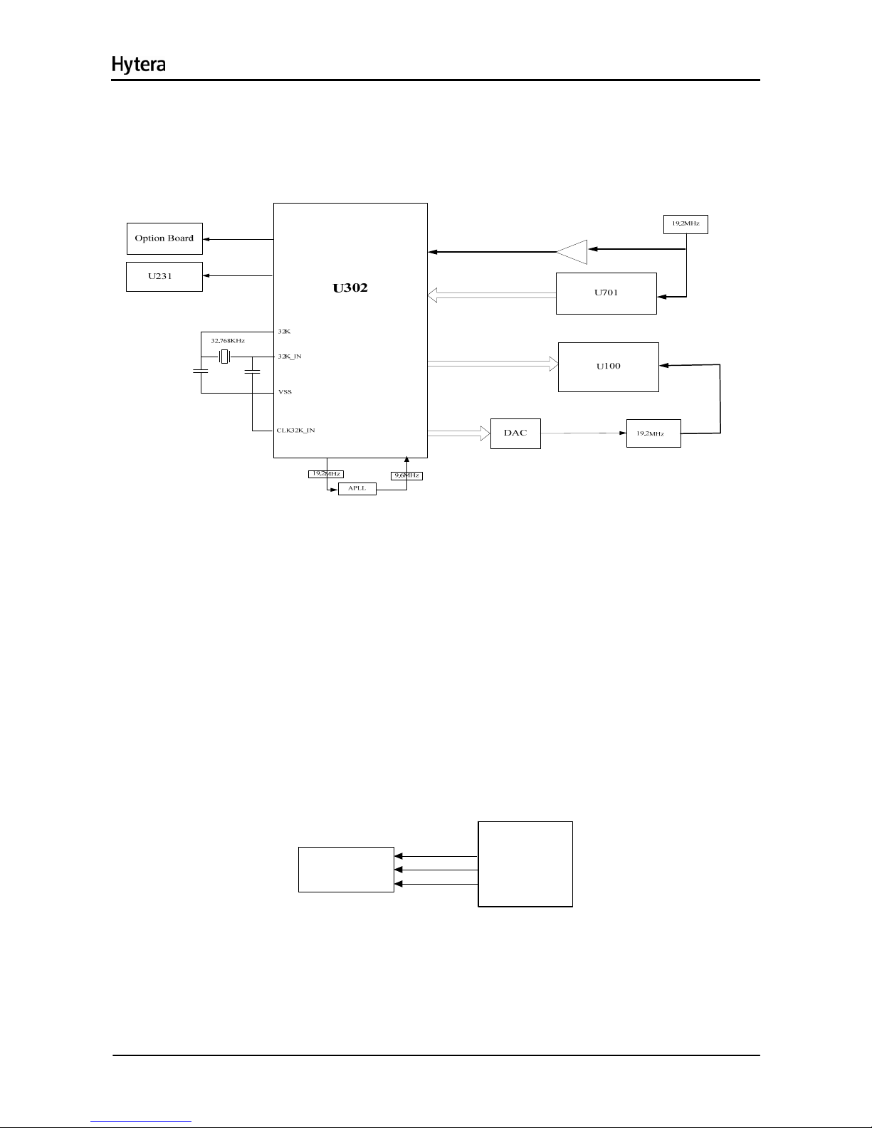
7.3 Clock
Figure 7-2 Diagram of Clock Distribution
7.3.1 Input Clock
The 32K clock provided by X375 is mainly used for timing and sleeping of the system. Its frequency
(32.768 kHz) is divided by U302 (32768 times in all) to 1Hz for counting seconds. The system clock
(19.2MHz) is generated by an external crystal oscillator.
7.3.2 Output Clock
The baseband outputs 3 clock signals fed to U231, U100 and Option Board respectively.
7.4 Interface Distribution
7.4.1 Serial Peripheral Interface (SPI)
SPIF.SCK
SPIF.DOUT
U302
SPIF.CS2PE
U701
PC
PD
Figure 7-3 Diagram of SPI Interface
SPI of U302 operates in Master Mode, and is controlled by MPU or DMA. In this case, U302 can provide
4 chip select signals, of which CS2 is used to control the IF processor U701.
7.4.2 MCSI Interface
11
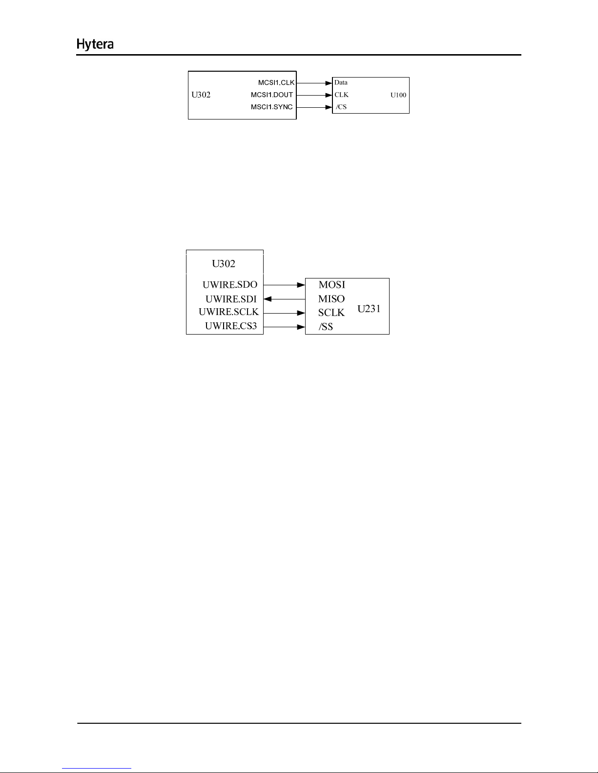
Service Manual
Figure 7-4 Diagram of MCSI Interface
When U302 is communicating with U100, it works in Master Mode with clock frequency of up to 9.6MHz.
U100 uses MCSI synchronization as chip select signal and MCSI1.DOUT as data cable to configure its
register.
7.4.3 MICROWIRE Interface
Figure 7-5 Diagram of MICROWIRE Interface
The MICROWIRE interface can accommodate 4 external devices at most, generally transmitting control
and status messages of external devices, and reading data from ROM. Its maximum clock frequency is a
quarter of system clock frequency. In this case, MICROWIRE is used to configure or read from the audio
processor. It requires chip select signal CS3.
7.4.4 Serial Synchronous Interface (SSI)
12
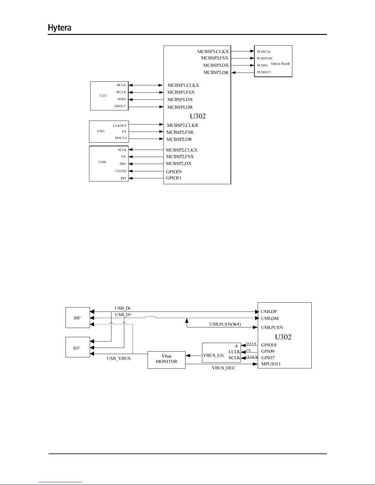
Service Manual
Figure 7-6 Diagram of SSI Interface
U302 has a total of three McBSP interfaces: McBSP1, McBSP2 and McBSP3, compatible with various
interfaces. McBSP1 is connected with I2C of the audio processor, to realize two-way transmission of
digital voice and data. McBSP2 uses independent clock and frame synchronization for transmitting and
receiving. The SSI of the receiver processor is connected with the RX end of McBSP2, and U500 with
the TX end of McBSP2. U302 works in Master Mode. McBSP3 is connected with the Option Board
interface for both voice and data transmission.
7.4.5 USB Interface
Figure 7-7 Diagram of USB Interface
The radio has two USB interfaces, which are connected to the same USB signal port of the processor.
REF CLOCK is the reference frequency in specified mode. It should be 12MHz in high rate mode or
1.5MHz in low rate mode.
7.4.6 UART Interface
13
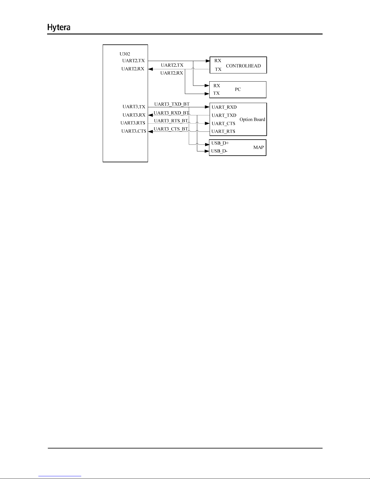
Service Manual
14
Figure 7-8 Diagram of UART Interface
U302 has a total of three UART interfaces, which are utilized to communicate with different external
devices. UART2 is used for communication with front panel and serial port on PC, while UART3 with
Option Board and accessory jack (USB).
7.4.7 Mobile Accessory Connector (MAC)
Mobile accessory connector contains audio interface, programmable I/O port, serial port, USB port,
accessory identifier port and etc, which are applied for further development. For details, please refer for
the section Interface Definition.
7.4.8 Option Board Interface
J400, an option board interface, is used to achieve specific function by connecting with the designated
option board. The definition of each pin is listed as below:
Service Manual
15
Pin
No.
Signal Function
I/O
Relative
to
Option
Board
Voltage
(VDD=3.3V)
Remarks
1
3
5
7
9
GPIO1
GPIO2
GPIO3
GPIO4
GPIO5
GPIO
GPIO
GPIO
GPIO
RESET-OUT
I/O
I/O
I/O
O
O
GPIO5: output
signal of the option
board (reset);
GPIO4 and GPIO5:
uni-directional
output interfaces.
They require their
input resistance is
above or equal to
47KΩ.
11
13
15
17
UART-TX
UART-RX
UART-CTS
UART-RTS
UART
O
I
I
O
UART
2
4
I2C –SDA
I2C -SCL
I2C
I/O
O
I2C
6
8
10
12
MCBSP-DR
MCBSP-WCLK
MCBSP-DX
MCBSP-FSX
MCBSP
I
I/O
O
I/O
VIH MIN=0.7VDD
VIL MAX=0. 3VDD
VOH MIN=0.8VDD
VOL
MAX=0.22VDD
McBSP:
Multichannel
Buffered Serial Port
14 AGND AGND
16 AF OB TO MB AF I
80mv (standard
output from the
option board to the
main board)
MAX:700mV
18 AF MB TO OB AF O
80mv (standard
output from the
main board to the
option board)
MAX:700mV
19 DGND DGND
20 3V6 or 5V Power O
Power supply:
5.0V
Service Manual
16
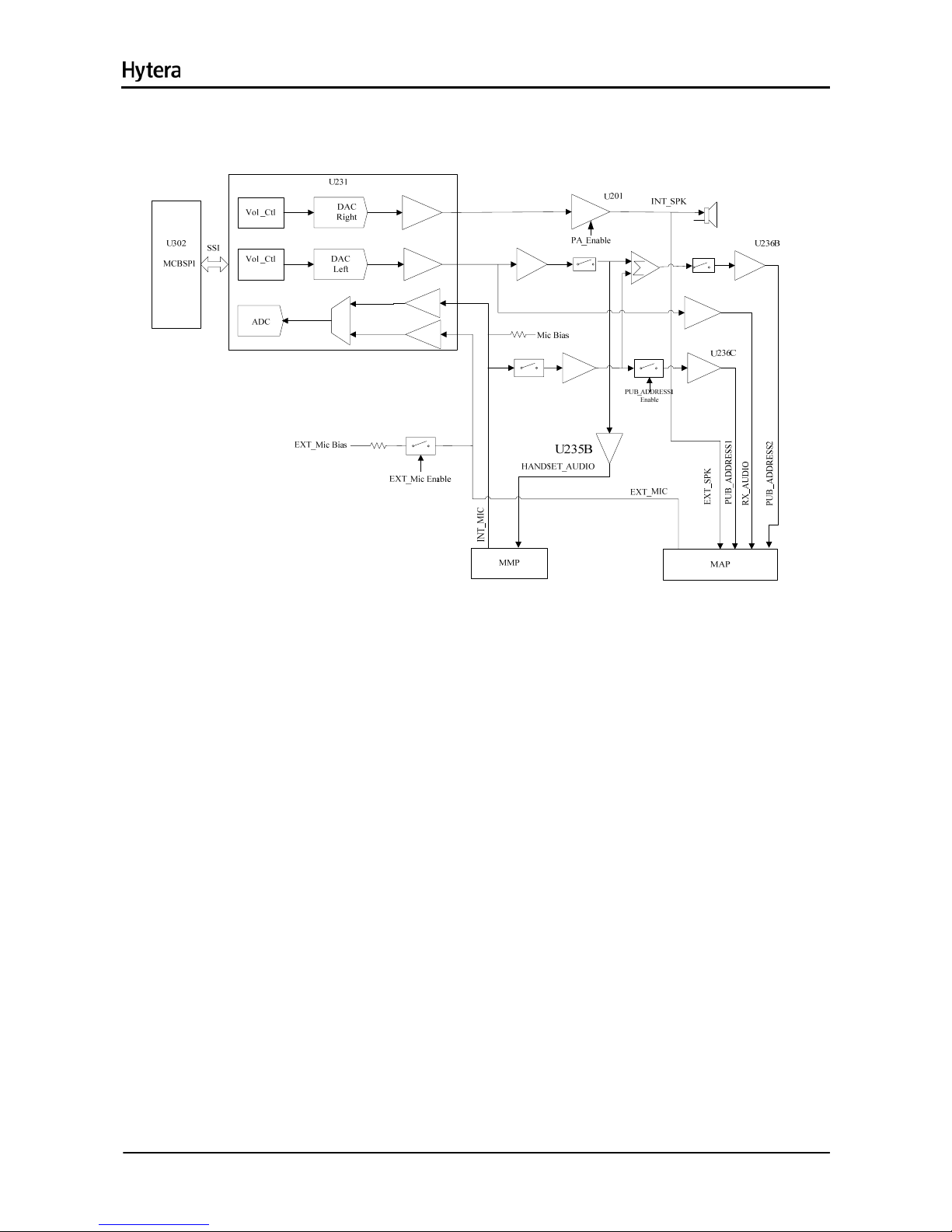
7.5 Audio Section
Figure 7-9 Diagram of Audio Section
7.5.1 RX Audio Circuit
U302 sends digital audio to the audio processor codec via the SSI bus of MCBSP1. This bus is
composed of CLKX, FSX, DX and DR. It sends the demodulated PCM audio signal to the codec, and
adjusts the signal to appropriate amplitude according to the volume (RMS should be 80mv when
frequency is 1 KHz and deviation is 3 KHz). Then the codec converts PCM data into analog audio data
via DAC. U231 provides two outputs: SPK1 and SPK2. SPK1 is amplified by U238 and then is fed to the
PA U201, to derive two outputs of received audio, which will be applied to the front panel speaker and
further development interface respectively. SPK2 is amplified and divided into the four paths of signal
HANDSET_AUDIO, RX_AUDIO, PUB_ADDESS1 and PUB_ADDESS2. The first two paths are
amplified by U235, and the last two paths are amplified by U236. Output of HANDSET_AUDIO,
PUB_ADDESS1 and PUB_ADDESS2 are controlled by Q231, Q235 and Q233 respectively.
7.5.2 TX Audio Circuit
The audio processor U231 has two MIC inputs: the internal MIC and external MIC. The internal MIC is
connected to the MICIN_HND of U231, and is combined with AUX1 to provide differential input. After
9.3V is divided by R255 and R264, a bias voltage of about 7V is provided to the front panel MIC. The

Service Manual
17
external MIC is connected to the MIC_HED of the codec as a unit-directional input. Both MICs are
controlled by Q232. When the internal MIC is active, EXT_MIC_EN is at low level, bias voltage of
external MIC is disconnected, and the ADC in U231 senses voltage at the MICIN_HND. When the
external MIC is active, EXT_MIC_EN is at high level, Q232 is turned on, bias voltage is connected, and
the ADC in U231 senses only audio data at MICIN_HED.
Audio signals input from the MMP interface or the accessory jack, are fed to the codec (gain of codec is
programmable via the CPS) and then are converted by the ADC into 16-bit PCM digital audio, which will
be fed to U302 via the SSI interface.
When the radio is set to operate in loudspeaker mode, audio signal is generated by the internal MIC, and
then feeds to U231, and finally is output via SPK2. The output audio signal is amplified, and then is
output as the two paths of audio PUB_ADDRESS1 and PUB_ADDRESS2.
Service Manual
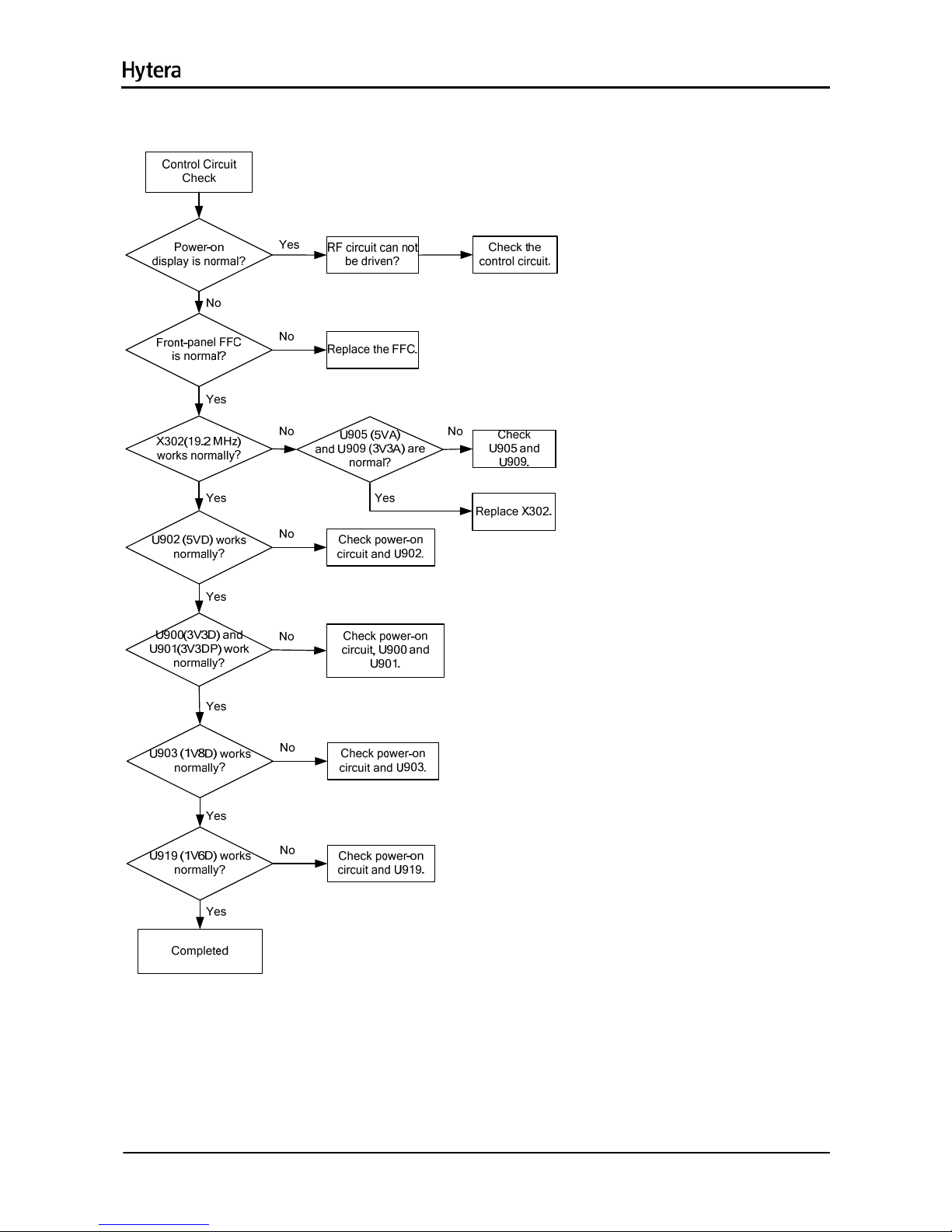
7.5.3 Troubleshooting Flow Chart for Control Circuit
18
Service Manual
7.6 PCB Difference
The UHF1 PCB has three versions: D, F and H.
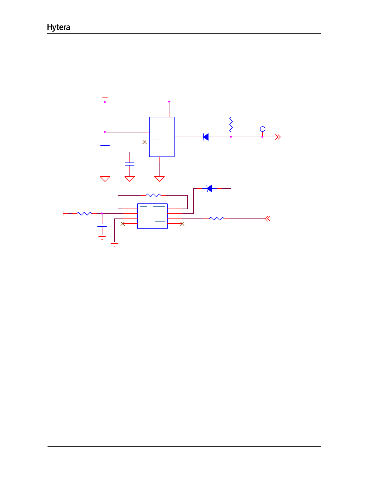
The watchdog circuit (in the figure below) is added in version F.
19
U906
RESET IC
MR
1
VCC
2
GND
3
PFI4PFO
5
WDI
6
/RST
7
WDO
8
R920 0
C978
0.1u
R983 0
RST_CTRL
R923 0
3V3D
D912
MBRM120LT1G
12
D913
MBRM120LT1G
12
R932
4.7K
C941
0.15u
U910
SENCE
5
VDD
6
RSET
1
GND
2
CT
4
MR
3
/PRST1
1
C937
1000p
3V3D
/PRST
Figure 7-10 Watchdog Circuit
Watchdog circuit
The watchdog circuit is used to prevent the radio from damage due to OMAP malfunction. If the program
works properly, U302 feeds pulse signal (25ms) to the watchdog circuit through RST_CTRL. Otherwise,
this pulse signal will be terminated and delayed for more than 1.6s so that U906 generates the reset
signal to reset OMAP.
Compared with version D & F, the difference in version G lies with the audio amplifier, which applies
TDA7297SA instead of TDA7297D.
Service Manual
8. GPS Circuit
8.1 Circuit Description
GPS
module
OMAP
UART
GPS
Antenna
LCD
Power
REB-1315LPx
Figure 8-1 Diagram of GPS Circuit
GPS positioning information can be acquired via the programmed GPS key on the front panel. The GPS
function is realized via REB-1315LPx module, which integrates GPS baseband processor circuits.
The GPS signal (1.57542GHz), received via the GPS active antenna (with a built-in LNA), goes to the
GPS module for processing, and then enters U302 via the UART port. Meanwhile, U302 sends control
command to the GPS module and forwards processed GPS information to the LCD.
8.2 Schematic Diagram
Figure 8-2 GPS Schematic Diagram
20
Service Manual
8.3 Parts List
No. Ref.No Part Number Description
1 R348 3001050000000 0Ω
2 R349 3001053300010 33Ω
3 R350 3001053300010 33Ω
4 R365 3001051030000 10KΩ
5 R366 3001051030000 10KΩ
6 C325 3101051040010 0.1UF
7 U326 3625999000030 GPS module
8 W321 4411100002000 IPX RF connector
9 R364 3001050000000 0Ω
10 R363 3001050000000 0Ω
11 L321 3212106390000 39nH
12 C330 3101051040010 0.1UF
13 L322 3221506300000 Ferrite bead
14 C333 3101081060010 10UF
15 C332 3101051040010 0.1UF
16 C331 3101081060010 10UF
17 R418 3001060000000 0Ω
18 R368 3001053300010 33Ω
19 R370 3001053300010 33Ω
21
Service Manual
8.4 Troubleshooting Flow Chart
Start
Antenna
works
normally?
No
Yes
Yes
No
The radio can position
normally?
`
Yes
Replace
defective
components.
No
Yes
The PC-based
software (e.g.SiRF
Demo) shows GPS
communication?
Yes
Replace U901.
Check R368 and
R370.
Check UART.
Yes
Yes
No
Replace the
GPS
module.
Active antenna is
damaged?
Replace
connector
W321.
No
U901 outputs 3.3V
normally?
Connector works
normally?
RX signal is
weak?
Peripheral
components work
normally?
Replace the active
antenna.
Yes
Replace the
antenna.
No
22

Service Manual
23
9. Tuning Description
For details about radio tuning, please refer to the help file of DMR Tuner Software supplied by the
Company.
Service Manual
24
10. Interface Definition
J404: to front panel jack
Pin No. Name Function
1 INT_MIC Audio input
2 MIC_GROUND Audio input ground
3 ACC_IO1 Accessory identifier pin 1
4 USB_VBUS USB power supply
5 HOOK HOOK
6 PTT PTT
7 USB_D- USB data cable D-
8 USB_D+ USB data cable D+
9 ACC_IO2 Accessory identifier pin 2
10 UART2_RXD_A Volume control port
11 UART2_TXD_B
12
HANDSET_AUDI
O
Audio signal output by accessory
13 SPKR1+ Speaker audio signal cable+
14 SPKR1- Speaker audio signal cable-
15 5VD Power supply
16 PRST Reset signal
17 KB_C0
18 KB_C1
19 KB_C2
20 KB_C3
21 KB_R0
22 KB_R1
23 KB_R2
Matrix keyboard
24 CSLED Backlight control IC chip select
25 CLOCK Backlight control IC clock
26 DATA Backlight control IC data
27 OE_LCD LCD read enable
28 WE_LCD LCD write enable
29 CS2_LCD LCD chip select
30 F_A1_LCD LCD register enable
31 F_D7
32 F_D6
33 F_D5
34 F_D4
35 F_D3
36 F_D2
LCD data bus
37 F_D1
38 F_D0
LCD data bus
39 GND Ground
 Loading...