

Page 1
Page 2

Contents
Introduction …………………………………………………………………………………… 1
Safety Information …………………………………………………………………………… 1
Radio Overview ……………………………………………………………………………… 3
Software Specifications …………………………………………………………………… 6
Circuit Description ………………………………………………………………………… 16
Semiconductor Data ……………………………………………………………………… 21
TM-800K Parts List 1 ……………………………………………………………………… 28
Tuning Description ………………………………………………………………………… 77
Terminal Function ………………………………………………………………………… 89
Troubleshooting Flow Chart ……………………………………………………………… 92
Disassembly and Assembly for Repair ………………………………………………… 96
Exploded View ……………………………………………………………………………… 98
TM-800K Parts List 2 ……………………………………………………………………… 99
Packing ……………………………………………………………………………………… 100
Specifications ……………………………………………………………………………… 123
Appendix 1 Entering Characters ……………………………………………………… 124
Page 3

TM-800K Service Manual
1
Introduction
Manual Scope
This manual is intended for use by experienced technicians familiar with similar types of
communication equipment. It contains all service information required for the equipment and is current
as of the publication date.
Safety Information
The following safety precautions shall always be observed during operation, service and repair of this
equipment.
z This equipment shall be serviced by qualified technicians only.
z Do not modify the radio for any reason.
z Use only HYT supplied or approved antenna.
z Gain of antenna must not exceed 3dBi for VHF or 5.5dBi for UHF.
z Mobile antenna Installation: Install the mobile antenna at least 82cm (32 inches) away from your
body, in accordance with the requirements of the antenna manufacturer/supplier.
z Transmit only when people inside and outside the vehicle are at least the minimum distance away
from a properly installed, externally mounted antenna.
z Mobile antenna substitution: Don’t substitute HYT supplied or approved antenna, or excessive
radio frequency radiation will result. Please contact your dealer or the manufacturer for further
instructions.
z Please make sure there’s no stress on the antenna joint during transportation or installation.
z To avoid electromagnetic interference and/or compatibility conflicts, turn off your radio in any area
where posted notices instruct you to do so. Hospital or health facilities may be using equipment
that is sensitive to external RF energy.
z For vehicles with an air bag, do not place a radio in the area over an air bag or in the air bag
deployment area.
z Turn off your radio prior to entering any area with explosive and flammable materials.
z Do not expose the radio to direct sunlight over a long time, nor place it close to heating source.
Page 4

TM-800K Service Manual
2
▇ Operation Guidelines
For vehicles equipped with electronic anti-skid braking systems, electronic ignition systems or
electronic fuel injection systems, interferences may occur during radio transmission. If the foregoing
electronic equipments are installed on your vehicle, please contact your dealer for further assistance to
make sure that radio transmission will not interfere with these equipments.
For radio installation in vehicles fueled by LP gas with LP gas container within interior of the vehicles,
the following precautions are recommended for personal safety.
1. Any space containing radio equipment shall be isolated by a seal from the space in which the LP
gas container and its fittings are located.
2. Remote (outside) fitting connections shall be used.
3. Good ventilation is required for the container space.
▇ Installation Guidelines
z Vehicle installation: The antenna can be mounted at the center of a vehicle metal roof or trunk lid if
the minimum safe distance is observed.
z Do not mount the mobile radio overhead or on a sidewall unless you take special precautions.
z If the mobile radio is not properly installed, road shock could bump the radio loose, and the falling
radio could, in some circumstances, cause serious injury to the driver or a passenger. In case of
vehicle accidents, even when properly installed, the radio could break loose and become a
dangerous projectile.
Page 5

TM-800K Service Manual
3
Radio Overview
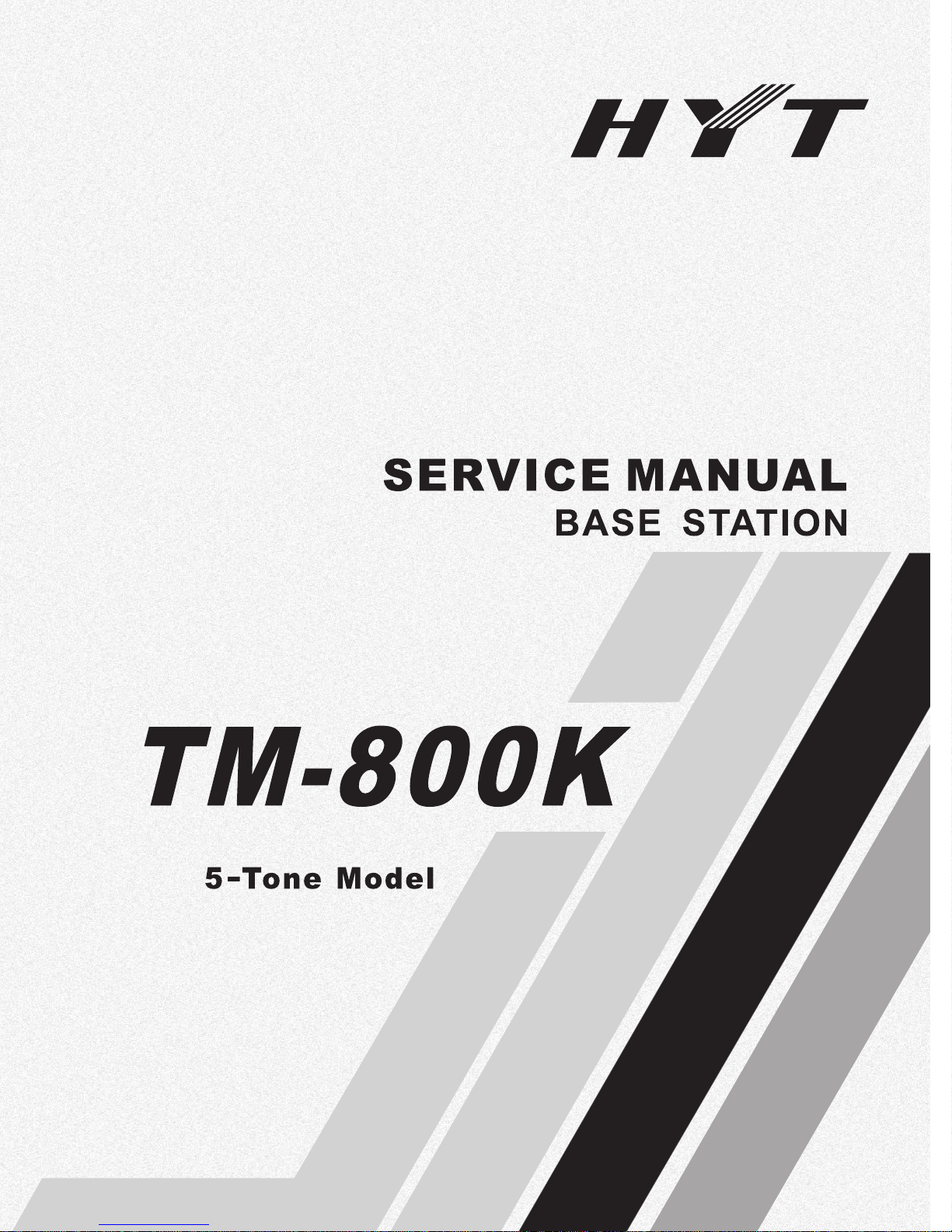
Front Panel View
1. Programmable Function Keys ( [ PF1 ] through [ PF6 ] )
Your dealer can program these keys as shortcuts to various radio features.
2. Microphone Jack
Plug a 6-pin connector into the jack.
3. Power Switch / Selector Knob
Press the power switch to turn the radio on/off.
The knob may be programmed by your dealer to select Volume Up / Down, Channel Up / Down,
and Zone Up / Down.
Turn the knob clockwise to adjust upwards and counter-clockwise to adjust downwards.
4. LCD Display
Please refer to the section “ LCD Display ”.
5. [ ▲ ] ( Up ) / [ ▼ ] ( Down ) Key
The keys may be programmed by your dealer to select Volume Up / Down, Channel Up / Down,
and Zone Up / Down.
6. LED Display
Used to display the operating status of main unit. Please refer to the section of “ LED Display ”.
7. Numeric Keys and Function Keys
Page 6
TM-800K Service Manual
4
Used when you select channel or transmit selective call etc.
8. Speaker
Used to output audio.
Microphone
LCD Display
Indicator Description
1. Display zone / channel number.
2. Display zone / channel alias ( up to 12 alphanumeric characters ).
3. Display channel frequency
4. Display the preprogrammed function
1. Display zone / channel number.
2. Display transmit power level ( H, M or L ).
3. Display the preprogrammed function.
Appears when the current channel is busy.
Appears when the Monitor key is pressed to monitor channel activities or
during a selective call.
Appears when Monitor key is pressed to unmute the speaker.
A
Appears when DTMF Live Dial mode or DTMF Keypad mode is enabled.
SCAN Appears while scanning.
CALL Appears when transmitting a selective call.
Appears when Scrambler is enabled
Appears when Compandor is enabled
Page 7
TM-800K Service Manual
5
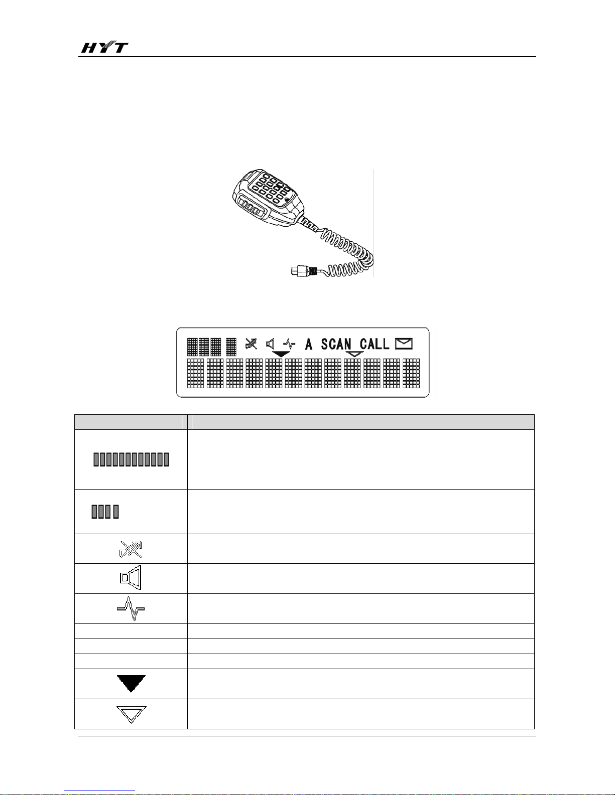
Rear Panel View
1. DB15
Further development interface.
2. DC power jack
Used to connect 13.6V DC power.
3. Fuse of DC power
4. Grounding terminal
5. Switch of AC power
6. Fuse of AC power
7. AC power jack
8. Antenna connector
Page 8

TM-800K Service Manual
6
Software Specifications
Radio Modes
Frame of Radio Modes
Keypad Entry for Mode Startup
MODE Main Menu Display/Sub Menu Operation Remarks
USER MODE Conventional Mode -------------------------------
Turn on the radio to enter
Conventional Mode
Test Mode -------------------------------
Adjust Mode -------------------------------
TEST &
ADJUST
MODE
Model Set Mode -------------------------------
While holding down [ PF2 ] key,
turn on the radio
Firmware Version Display Mode -------------------------------
While holding down [ PF3 ] key,
turn on the radio
Firmware Programming Mode -------------------------------
While holding down [ PF4 ] key,
turn on the radio
Wired Clone Mode -------------------------------
While holding down [ PF5 ] key,
turn on the radio
PC Programming Mode ------------------------------- Receive commands from PC
Note: When power-on password is enabled, you must input the correct password before you can
enter User Mode.
You can input password through the keypad and press [ # ] to clear.
Error Information and Measures in User Mode
The radio self-checks when power on. If no error is detected, the radio enters conventional mode.
While the radio will sound alert once any error is checked.
Firmware Programming Mode
PC Programming Mode
Clone Mode Wired Clone Mode
User Mode
Conventional Mode
Model Set Mode
Test & Adjust Mode
Page 9

TM-800K Service Manual
7
Error information and measures:
No. Error Information LCD Display Measures
1 Stun status Stun Re-program.
2 Data and Firmware Version
mismatch
No Data
Re-program with programming software of right
version.
Firmware Programming Mode
The built-in FLASH ROM enables user to add new functions simply by upgrading.
(1) Turn on the radio while holding down [ PF4 ] simultaneously to enter Firmware Programming
Mode, “ PC Program ” appears on the LCD.
(2) Run the programming software.
(3) Connect the radio with a PC by programming cable.
(4) Select the corresponding COM port, and then click “ Download ”.
(5) When data is successfully written into the radio, click “ OK ” to exit.
(6) Repeat step 1 through 5 to program another radio.
Note: The radio can’t enter the Firmware Programming Mode if it is disabled by your dealer.
It can be set ON only after being programmed through the programming software.
Firmware Version Display Mode
Turn the radio on while holding down [ PF3 ] to enter Firmware Version Display Mode, the firmware
version will be displayed on the LCD.
Release [ PF3 ] to enter User Mode.
PC Mode
Connect the radio with a PC by programming cable. If data is written to the radio from PC, it can be
programmed into the FLASH. Data programming is accessible by programming software.
When data is written to the radio from PC, “ PROGRAMMING ” appears on the LCD. LED glows green
when data is written to the radio and red when data is read from the radio. Radio will restart automati-
cally when programming is completed.
Wired Clone Mode
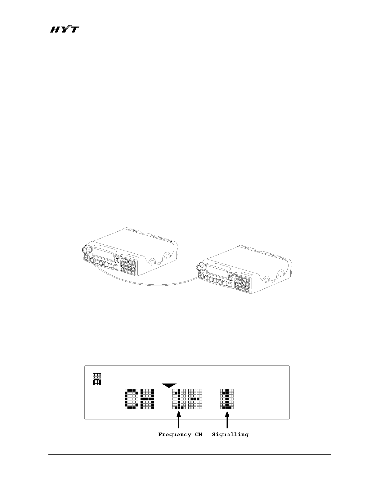
Data can be transmitted from radio to radio by wired cloning.
(1) Turn on the source radio while holding down [ PF5 ] simultaneously, the radio enters Clone
Mode with “CLONE” on the LCD, or enters User Mode if Clone Mode is disabled by your dealer.
Page 10
TM-800K Service Manual
8
(2) Press [ PF2 ] to toggle between Dealer Clone and Factory Clone Mode. “Dealer Clone” or
“Factory Clone” appears on the display when the corresponding mode is selected. The radio
restores the original display after 5 seconds.
Unlike Factory Clone Mode, tuning settings and embedded messages are not covered in Dealer
Clone Mode.
Dealer Clone Mode is the default mode.
(3) Connect the two radios by clone cable, and then turn on the target radio.
(4) Press [ PF6 ] to start cloning, the LED of source radio glows red and that of target radio glows
green during cloning. “PROGRAMMING” is also displayed on the target radio. “END” appears on
the source radio when cloning is completed and the target radio displays “END” when all data is
received.
(5) Press [ PF6 ] to return to Clone Mode. “CLONE” appears on the source radio. Repeat the above
steps to continue wired cloning.
Note: Cloning is available only when both radios are in the same mode.
Test Mode
1. Turn the radio on while holding down [ PF2 ], the radio enters Test Mode. Test frequency channel
and signalling test channel are displayed.
Page 11

TM-800K Service Manual
9
In this mode, the channel frequency ( center, low, high ) can be modified through the programming
software.
Test frequency channels are shown in the following table:
Model RX / TX CH1 ( C ) CH 2 ( L ) CH 3 ( H ) CH 4 CH 5 CH 6 CH 7 CH 8
RX(MHz)
155.15
136.15 173.85 145.55 164.55 155.00 155.20 155.40136-174M
(V)
TX(MHz) 155.00 136.00 174.00 145.50 164.50 155.00 155.20 155.40
RX(MHz)
481.15 450.15
511.85
465.55
496.55
481.00 481.20 481.40
450-512M
(U2)
TX(MHz)
481.00 450.00 512.00
465.50
496.50 481.00 481.20 481.40
RX(MHz)
375.15 350.15 399.85
362.55
387.55 375.00 375.20 375.40
350-400M
(U5)
TX(MHz)
375.00 350.00 400.00
362.50
387.50 375.00 375.20 375.40
RX(MHz)
435.15 400.15 469.85
417.55
452.55 435.00 435.20 435.40
400-470M
(U1)
TX(MHz)
435.00 400.00 470.00
417.50
452.50 435.00 435.20 435.40
RX(MHz) 465.15 440.15 489.85 452.55 477.55 465.00 465.20 465.40440-490M
(U4)
TX(MHz) 465.00 440.00 490.00 452.50 477.50 465.00 465.20 465.40
RX(MHz)
503.15 480.15 525.85
491.75
515.25 503.00 503.20 503.40
480-526M
(U3)
TX(MHz)
503.00 480.00 526.00
491.70
515.20 503.00 503.20 503.40
RX(MHz) 425.15 400.15 449.85 412.55 437.55 425.00 425.20 425.40400-450M
(U6)
TX(MHz) 425.00 400.00 450.00 412.50 437.50 425.00 425.20 425.40
RX(MHz) 485.15 450.15 519.85 467.55 502.55 485.00 485.20 485.40450-520M
(U7)
TX(MHz) 485.00 450.00 520.00 467.50 502.50 485.00 485.20 485.40
Signallings are shown as follows:
No. RX TX Description
1 None None
2 None 100Hz square wave
3 CTCSS 67.0Hz CTCSS 67.1Hz
4 CTCSS 151.4Hz CTCSS 151.4Hz
5 CTCSS 210.7Hz CTCSS 210.7Hz
6 CTCSS 250.3Hz CTCSS 250.3Hz
7 CDCSS 023N CDCSS 023N
8 CDCSS 754I CDCSS 754I
9 None DTMF (159D)
10 None DTMF 9
11 None 5-Tone ( 037BC ( EEA ) )
12 None Single tone 1200Hz
13 None Single tone 1000Hz
14 None None
2. In Test Mode, the following functions can be accomplished by key press:
Page 12
TM-800K Service Manual
10
Key Function Description
Up Volume Up
Down Volume down
PF1 Wide/Medium/Narrow band
PF2 Squelch Open / Close
“
” icon appears when squelch is open.
PF3 Test Mode / Adjust Mode
PF4 Activate compandor function
PF1: enable / disable compandor
PF2: enable / disable clock shift
PF3: 1200 / 2400bps MSK
PF5 Signalling Up
PF6 Signalling Down
Selector Knob Channel Up/Down
In Test Mode, press [ PF4 ], then press the following key to enable the corresponding functions.
PF1 Enable / disable Compandor “ ▼ ” icon appears when compandor is enabled
PF2 Enable / disable Clock Shift “ A ” icon appears when clock shift is enabled
PF3 1200 / 2400bps MSK “ ” icon appears when 2400bps is selected
PF4 Return to Test Mode
PF5 None
PF6 None
3. In Test Mode, press [ PF3 ] to enter Adjust Mode. Turn the Selector Knob to choose your desired
setting items.
No. Adjust Item LCD Display
1 Frequency stability Frequency
2 TX power Tx Power
3 Max. deviation Max.Deviate
4 CDCSS balance CDCSSBalance
5 CTCSS deviation CTCSSDeviate
6 CDCSS deviation CDCSSDeviate
7 DTMF deviation DTMFDeviate
8 MSK deviation MSK Deviate
9 Single tone deviation Tone Deviate
10 RX sensitivity Rx Sensitivity
11 Squelch open level Open SQL
12 SQL close level Close SQL
13 Rssi High High Rssi
14 Rssi Low Low Rssi
15 DI Deviation DI Deviate
Page 13
TM-800K Service Manual
11
In Test Mode, user can press the following key to switch menu modes.
Press [ PF3 ] to toggle between Test Mode and Adjust Mode.
Press [ PF4 ] to toggle between Adjust Mode and Model Set Mode ( [ PF4 ] is invalid if Model
Set Mode is disabled by your dealer. Refer to Model Set Mode for details ).
Press [ PF6 ] to enter the selected mode.
4. In Adjust Mode, the following functions can be accomplished by key press.
Key Function Description
Up Volume Up
Down Volume Down
PF1 Return to Tuning Item menu
PF2 Squelch Open / Close
“
” icon appears when squelch is open.
PF4 Enter the previous item ( Down )
PF5 Enter the next item ( Up )
PF6 Save the settings, enter the next item
Selector Knob Adjust upwards / downwards
5. Setting Items (***: 1-256)
Setting Item
Wide/ Medium/
Narrow band
Frequency Main LCD Sub LCD Description
Frequency Stability Wide Center Freq *** C No signalling
Center Hi Power *** C No signalling
Low Hi Power *** L No signalling
High Hi Power *** H No signalling
Center Mi Power *** C No signalling
Low Mi Power *** L No signalling
High Mi Power *** H No signalling
Center Lo Power *** C No signalling
Low Lo Power *** L No signalling
Tx Power High power
High Lo Power *** H No signalling
Center Max Dev *** C No signalling
Low Max Dev *** L No signalling
Wide
High Max Dev *** H No signalling
Medium Center Max Dev *** m C No signalling
Center Max Dev *** n C No signalling
Low Max Dev *** n L No signalling
Max. deviation
Narrow
High Max Dev *** n H No signalling
CDCSS Balance Wide
Center CDCSS BAL*** C
CDCSS: 023N
Page 14

TM-800K Service Manual
12
Low CDCSS BAL*** L
CDCSS: 023N
High CDCSS BAL*** H
CDCSS: 023N
Medium Center CDCSS BAL*** m C
CDCSS: 023N
Center CDCSS BAL*** n C
CDCSS: 023N
Low CDCSS BAL*** n L
CDCSS: 023N
Narrow
High CDCSS BAL*** n H
CDCSS: 023N
Center 67.0 DEV*** C CTCSS: 67.0Hz
Low 67.0 DEV*** L CTCSS: 67.0Hz
Wide
High 67.0 DEV*** H CTCSS: 67.0Hz
Medium Center 67.0 DEV*** m C CTCSS: 67.0Hz
Center 67.0 DEV*** n C CTCSS: 67.0Hz
Low 67.0 DEV*** n L CTCSS: 67.0Hz
Narrow
High 67.0 DEV*** n H CTCSS: 67.0Hz
Center 151.4 DEV*** C CTCSS: 151.4Hz
Low 151.4 DEV*** L CTCSS: 151.4Hz
Wide
High 151.4 DEV*** H CTCSS: 151.4Hz
Medium Center 151.4 DEV*** m C CTCSS: 151.4Hz
Center 151.4 DEV*** n C CTCSS: 151.4Hz
Low 151.4 DEV*** n L CTCSS: 151.4HzNarrow
High 151.4 DEV*** n H CTCSS: 151.4Hz
Center 254.1 DEV*** C CTCSS: 254.1Hz
Low 254.1 DEV*** L CTCSS: 254.1Hz
Wide
High 254.1 DEV*** H CTCSS: 254.1Hz
Medium Center 254.1 DEV*** m C CTCSS: 254.1Hz
Center 254.1 DEV*** n C CTCSS: 254.1Hz
Low 254.1 DEV*** n L CTCSS: 254.1Hz
CTCSS deviation
Narrow
High 254.1 DEV*** n H CTCSS: 254.1Hz
Center CDCSS DEV*** C CDCSS: 023N
Low CDCSS DEV*** L CDCSS: 023N
Wide
High CDCSS DEV*** H CDCSS: 023N
Medium Center CDCSS DEV*** m C CDCSS: 023N
Center CDCSS DEV*** n C CDCSS: 023N
Low CDCSS DEV*** n L CDCSS: 023N
CDCSS deviation
Narrow
High CDCSS DEV*** n H CDCSS: 023N
Center DTMF DEV *** C DTMF: 9
Low DTMF DEV *** L DTMF: 9
Wide
High DTMF DEV *** H DTMF: 9
Medium Center DTMF DEV *** m C DTMF: 9
DTMF deviation
Narrow
Center DTMF DEV *** n C DTMF: 9
Page 15

TM-800K Service Manual
13
Low DTMF DEV *** n L DTMF: 9
High DTMF DEV *** n H DTMF: 9
Center MSK DEV *** C No signalling
Low MSK DEV *** L No signalling
Wide
High MSK DEV *** H No signalling
Medium Center MSK DEV *** m C No signalling
Center MSK DEV *** n C No signalling
Low MSK DEV *** n L No signalling
MSK deviation
Narrow
High MSK DEV *** n H No signalling
Center TONE DEV *** C 1KHz
Low TONE DEV *** L 1KHz
Wide
High TONE DEV *** H 1KHz
Medium Center TONE DEV *** m C 1KHz
Center TONE DEV *** n C 1KHz
Low TONE DEV *** n L 1KHz
Tone deviation
Narrow
High TONE DEV *** n H 1KHz
-
Low
Rx Sens. ***
L
No signal,SQL off
-
Center/
Low Rx Sens. ***
CL
No signal,SQL off
- Center
Rx Sens. ***
C
No signal,SQL off
-
High/
Center Rx Sens. ***
HC
No signal,SQL off
RX Sensitivity
-
High
Rx Sens. ***
H
No signal,SQL off
Center OpenSQL9 *** C No signalling
Low OpenSQL9 *** L No signalling
SQL 9 Wide
High OpenSQL9 *** H No signalling
SQL 9 Medium Center OpenSQL9 *** m C No signalling
Center OpenSQL9 *** n C No signalling
Low OpenSQL9 *** n L No signalling
SQL 9 Narrow
High OpenSQL9 *** n H No signalling
Center OpenSQL3 *** C No signalling
Low OpenSQL3 *** L No signalling
SQL 3 Wide
High OpenSQL3 *** H No signalling
SQL 3 Medium Center OpenSQL3 *** m C No signalling
Center OpenSQL3 *** n C No signalling
Low OpenSQL3 *** n L No signalling
SQL Open
SQL 3 Narrow
High OpenSQL3 *** n H No signalling
Center CloseSQL9*** C No signalling
SQL Close SQL 9 Wide
Low CloseSQL9*** L No signalling
Page 16
TM-800K Service Manual
14
High CloseSQL9*** H No signalling
SQL 9 Medium Center CloseSQL9*** m C No signalling
Center CloseSQL9*** n C No signalling
Low CloseSQL9*** n L No signalling
SQL 9 Narrow
High CloseSQL9*** n H No signalling
Center CloseSQL3*** C No signalling
Low CloseSQL3*** L No signalling
SQL 3 Wide
High CloseSQL3*** H No signalling
SQL 3 Medium Center CloseSQL3*** m C No signalling
Center CloseSQL3*** n C No signalling
Low CloseSQL3*** n L No signalling
SQL 3 Narrow
High CloseSQL3*** n H No signalling
Center High RSSI *** C No signalling
Low High RSSI *** L No signalling
Wide
High High RSSI *** H No signalling
Medium Center High RSSI *** m C No signalling
Center High RSSI *** n C No signalling
Low High RSSI *** n L No signalling
RSSI High Level
Narrow
High High RSSI *** n H No signalling
Center Low RSSI *** C No signalling
Low Low RSSI *** L No signalling
Wide
High Low RSSI *** H No signalling
Medium Center Low RSSI *** m C No signalling
Center Low RSSI *** n C No signalling
Low Low RSSI *** n L No signalling
RSSI Low Level
Narrow
High Low RSSI *** n H No signalling
Center DI Deviate C No signalling
Low DI Deviate L No signalling
Wide
High DI Deviate H No signalling
Medium Center DI Deviate mC No signalling
Center
DI Deviate nC No signalling
Low
DI Deviate nL No signalling
DI Deviation
Narrow
High
DI Deviate nH No signalling
Model Set Mode
1. Turn the radio on while holding down [ PF2 ], the radio enters Test Mode. The test frequency
channel and signalling test channel are displayed.
2. In Test Mode, press [ PF3 ] to enter Adjust Mode.
3. In Adjust mode, press [ PF4 ] to enter Model Set Mode. “Frequency Range” is displayed.
Page 17
TM-800K Service Manual
15
4. Turn the Selector Knob to choose model.
5. Press [ PF6 ] to confirm. ”Wait a second…” is displayed.
6. Press [ PF3 ] to return to Test Mode.
Notes:
1. Once the new model is set, previous channel settings ( frequency, CTCSS / CDCSS, channel
function settings ) will be deleted, and part of functions are also changed. Therefore, do not
make this operation unless it’s a must, such as changing the EEPROM or FLASH ROM, etc.
2. Initial Data Table
Model RX / TX
CH 1
(Center )
CH 2
(Low)
CH 3
(High )
CH 4 CH 5 CH 6 CH 7 CH 8
RX (MHz) 155.15 136.15 173.85 145.55 164.55 155.00 155.20 155.40
136-174M
(V)
TX (MHz) 155.00 136.00 174.00 145.50 164.50 155.00 155.20 155.40
RX (MHz) 481.15 450.15 511.85 465.55 496.55 481.00 481.20 481.40
450-512M
(U2)
TX (MHz) 481.00 450.00 512.00 465.50 496.50 481.00 481.20 481.40
RX (MHz) 375.15 350.15 399.85 362.55 387.55 375.00 375.20 375.40
350-400M
(U5)
TX (MHz) 375.00 350.00 400.00 362.50 387.50 375.00 375.20 375.40
RX (MHz) 435.15 400.15 469.85 417.55 452.55 435.00 435.20 435.40
400-470M
(U1)
TX (MHz) 435.00 400.00 470.00 417.50 452.50 435.00 435.20 435.40
RX (MHz) 465.15 440.15 489.85 452.55 477.55 465.00 465.20 465.40
440-490M
(U4)
TX (MHz) 465.00 440.00 490.00 452.50 477.50 465.00 465.20 465.40
RX (MHz) 503.15 480.15 525.85 491.75 515.25 503.00 503.20 503.40
480-526M
(U3)
TX (MHz) 503.00 480.00 526.00 491.70 515.20 503.00 503.20 503.40
RX (MHz) 425.15 400.15 449.85 412.55 437.55 425.00 425.20 425.40
400-450M
(U6)
TX (MHz) 425.00 400.00 450.00 412.50 437.50 425.00 425.20 425.40
485.15 450.15 519.85 467.55 502.55 485.00 485.20 485.40 485.15450-520M
(U7)
485.00 450.00 520.00 467.50 502.50 485.00 485.20 485.40 485.00
Page 18
TM-800K Service Manual
16
Circuit Description
Frequency Configuration
The receiver utilizes double conversion superheterodyne. The first IF is 49.95MHz (VHF) / 73.05MHz
(UHF) and the second is 450 KHz. The first local oscillator signal is supplied by PLL circuit. The second
local oscillator signal (73.5MHz) of UHF model is generated from TCXO (73.5MHz); the second local
oscillator signal (50.4MHz) of VHF model is generated from the frequency tripling of TCXO (16.8MHz).
The PLL circuit also generates the frequencies needed in the transmitter ( See Fig.2 ).
Frequency Range: 136 MHz - 174MHz
U1: 400 MHz - 470MHz U2: 450 MHz - 512MHz
U3: 480 MHz - 526MHz U4: 440 MHz - 490MHz
U5: 350 MHz - 400MHz U7: 450 MHz - 520MHz
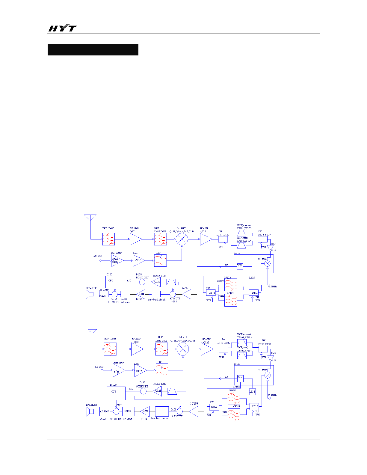
Receiver Circuit
The receiver section configuration is shown as Fig. 1.
Figure 1-a UHF Receiver Section Configuration
Figure 1-b VHF Receiver Section Configuration
Page 19

TM-800K Service Manual
17
RF AMP BPF
It consists of BPF (D603, D602, and D601) and RF amplifier (Q601). The range of bandpass frequency
(V: 136 MHz - 174MHz, U1: 400 MHz - 470 MHz; U2: 450 MHz - 512MHz; U3: 480 MHz - 526MHz; U4:
440 MHz - 490MHz; U5: 350 MHz - 400MHz; U7: 450 MHz - 520MHz). The signal is filtered by the RF
Amp BPF to eliminate unwanted signals before going to the first mixer.
The First Mixer
The signal from RF AMP BPF is mixed with the first local oscillator signal from PLL circuit in the
double-balance mixer (Q138, Q144, Q145, and Q146) to generate a 73.05MHz (UHF) / 49.95MHz
(VHF) first IF signal. The first IF signal is then fed through two crystal filters (N: XF101, XF103; W:
XF102, XF104) to further remove spurious signals.
IF Amplifier
The first IF signal is amplified by Q125, Q118 and then enters IC119 (TA31136FN). The signal is mixed
with the second local oscillator signal (UHF: 73.5MHz; VHF: 50.4MHz) to create a 450 KHz second IF
signal. The second IF signal is then fed to a ceramic filter (N: CF103; W: CF104) to eliminate unwanted
signals. The resulting signal is detected by IC119 and output from Pin9 as an AF signal.
Audio Amplifier
The audio signal from IC119 is amplified by IC109 before being filtered. The resulting AF signal passes
through Q108 (AF MUTE) and IC121 (electronic switch), then is amplified by IC106 (the received
signalling is inputted into CPU for decoding) and IC104. The amplified signal is fed to IC125 (volume
control) and Q114 (SP MUTE) before entering AF AMP (IC126). The outputted AF signal is then
delivered to the speaker through control panel.
Squelch
The audio signal from IC119 is amplified by IC109 again, and then filtered to remove noise signals.
The noise signal is amplified by Q121 and rectified by D110 to produce an ASQ level. The ASQ level is
then compared in CPU (IC120) to generate a level which controls AF MUTE and SP MUTE. IC120
determines whether to output sounds from the speaker by controlling Q108, Q114.
Page 20
TM-800K Service Manual
18
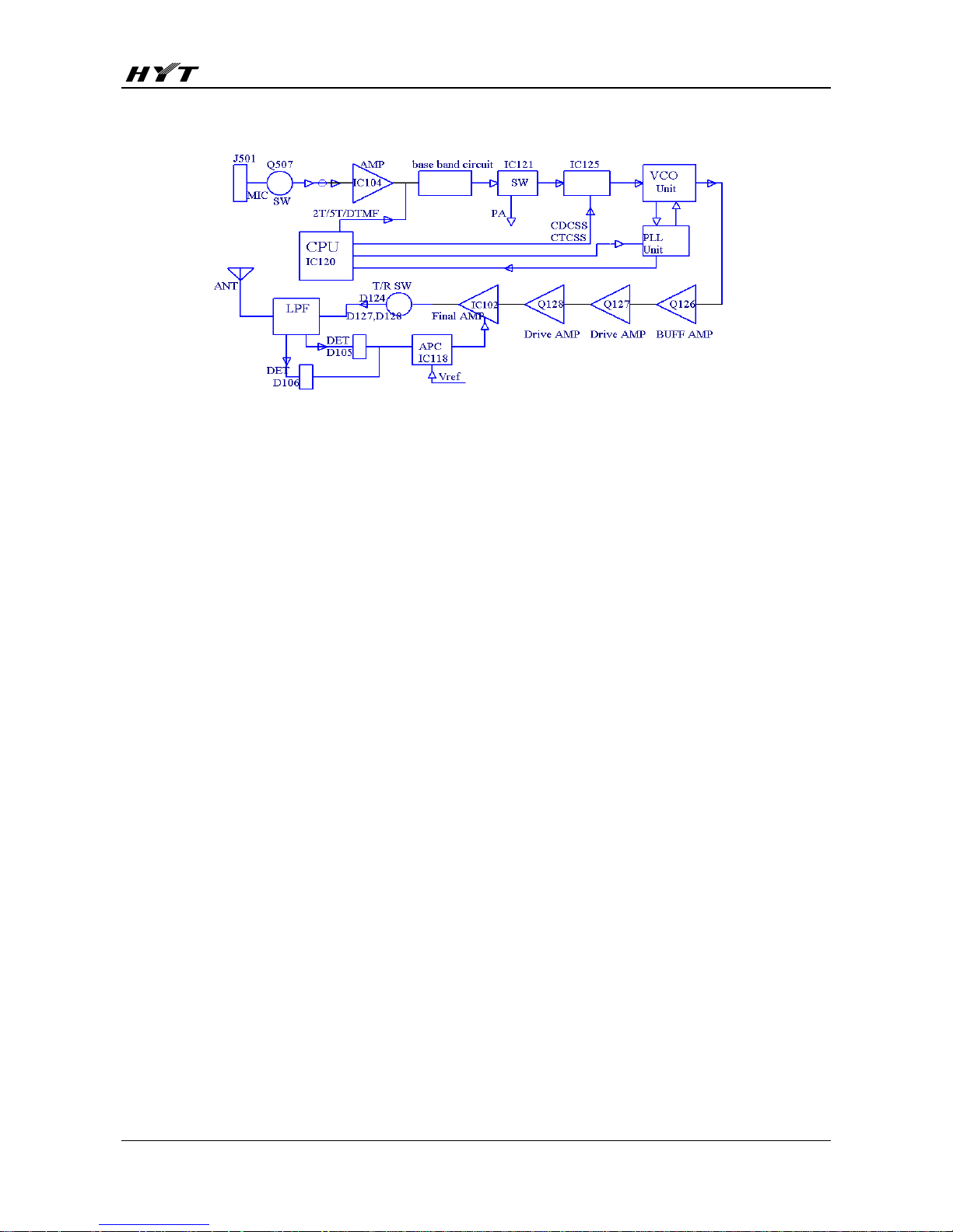
Transmitter Circuit
Figure 2 Transmitter Section Configuration
MIC Circuit and Modulation Circuit
The AF signal from MIC is amplified by IC104 after passing through the MIC control switch (Q507). The
resulting signal is then amplified by IC106 and pre-emphasized, encoded. It is passed to IC121 (electronic
switch) before reaching IC125. The signalling is inputted into IC125 and enters VCO for modulation.
Driver and Final-Stage Power Amplifier Circuit
TX-RF signal is outputted from Q703 in VCO circuit and amplified by Q126, Q127 and Q128. The
amplified signal is then fed to IC102 (Power Module) and passes through LPF before reaching the
antenna terminal.
APC
The APC is used to keep the power output at a constant preset value. D105 and D106 transform the
signal from detector into DC voltage which is then compared with the reference voltage from CPU in
IC118 and outputted as DC control voltage. The DC control voltage controls the output power by
controlling the grid of IC102.
PLL Circuit
PLL circuit generates the first local oscillator signal for reception and the RF signal for transmission.
PLL circuit consists of TX frequency oscillator (Q701), RX frequency oscillator (Q702), buffer amplifier
(Q703), RF amplifier (Q124), PLL IC (IC801), LPF (Q804, Q805) and TX/RX VCO control switch
(Q704, Q706).
In transmit mode, IC120 transmits the frequency data to PLL IC. Q704 is turned on to activate TX VCO.
Page 21
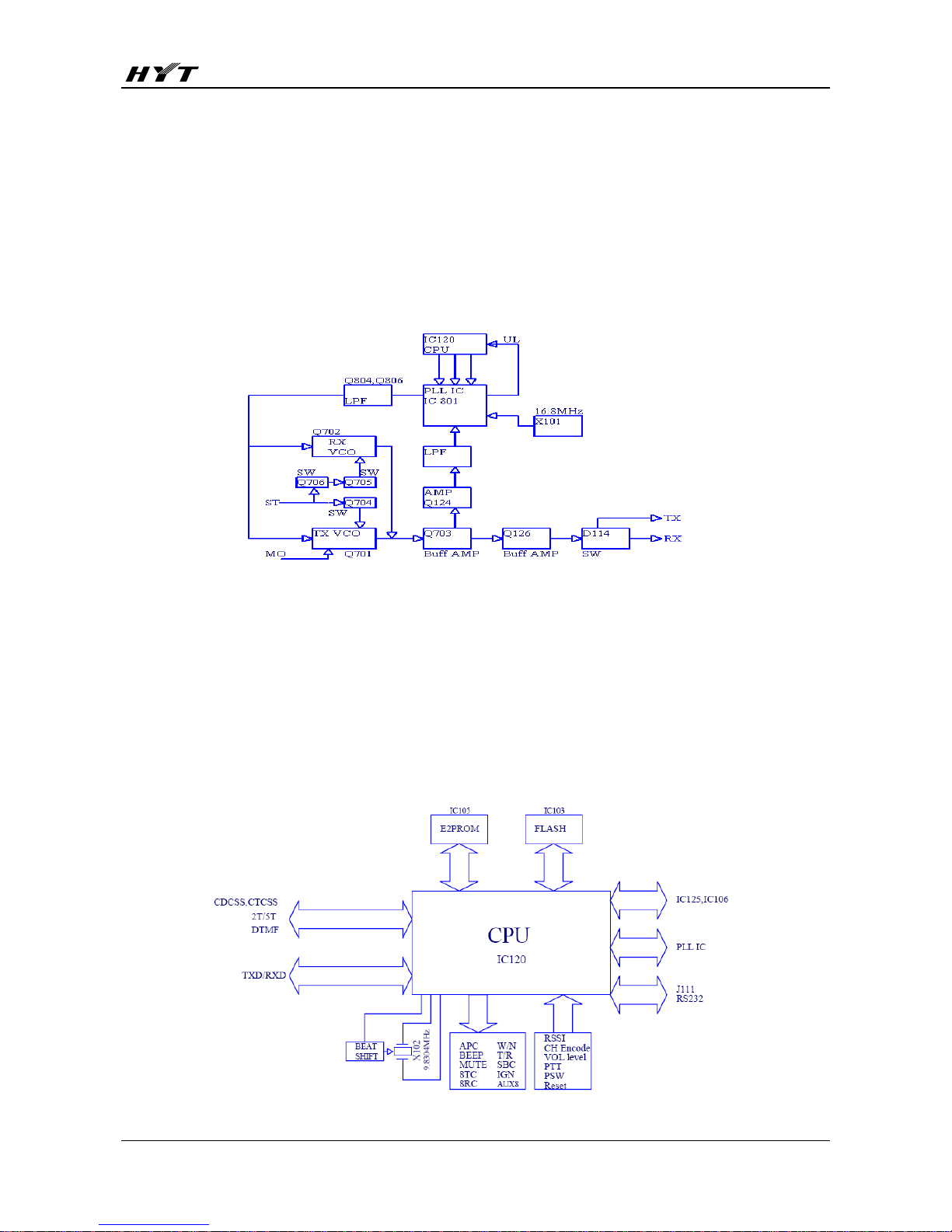
TM-800K Service Manual
19
The outputted signal is amplified by Q703, Q124, and then divided by PLL IC into 2.5KHz, 5KHz or
6.25KHz signal. The divided signal is compared with 2.5KHz, 5KHz or 6.25KHz reference signal from
16.8MHz crystal oscillator (2.5 PPM frequency stability) in the phase comparator. The frequency control
voltage outputted from the phase comparator is sent to TX VCO after passing through LPF (Q804,
Q805). In the meantime, modulation signal (TX) is passed to TX VCO for frequency modulation.
The working principle in receive mode is similar to that in transmit mode.
Figure 3 PLL Circuit
Control Circuit
Circuit in this section is comprised of CPU, reset IC, power supply controller and flash ROM.
CPU
IC120 (CPU) operates at 9.8304MHz. It controls the data transmission between receive circuit,
transmit circuit, control circuit, display circuit and peripheral circuit.
Figure 4 Control Circuit
Page 22
TM-800K Service Manual
20
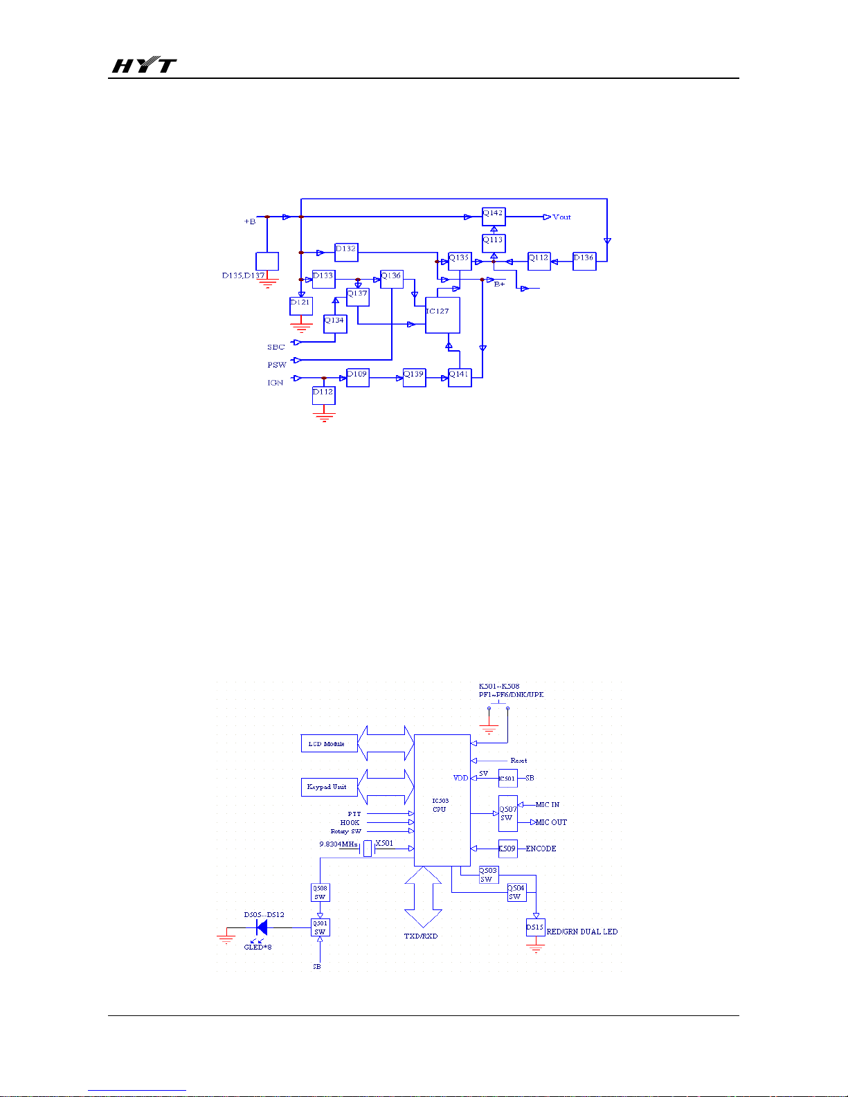
Power Supply
Power supply of the radio is derived from the battery which supplies battery B+. D135 and D137 are
over-voltage protection Diodes. Power-on/off can be controlled by software.
Figure 5 Power Switch Circuit
Vout provides power supply to IC115, IC114, IC113, and IC111, which produces 8V, 9V, 5V, and 3.3V
voltage to the circuit.
Display Circuit
Display circuit is comprised of CPU (IC503), LCD module, LED and other components. Radio features
are programmable by PF1-PF6. Data is displayed on the 12-digit and 4-digit dot matrix LCD in
alphanumeric form.
Figure 6 Display Circuit
Page 23
TM-800K Service Manual
21
Semiconductor Data
1. Voltage Supply: TA7805F (Display Unit IC501): Providing supply voltage.
2. Voltage Detector: R3111H421C (Display Unit IC502)
2-1. Pin Function
Pin No. Name I/O Function
1 Vout O Reset.
2 GND GND.
3 Vin I Supply voltage.
3. Display CPU: UPD78F0511GB (Display Unit IC503)
3-1.Pin Function
Pin No. Name I/O Function
1 P41
2 P40 O SHIFT
3 RESET
4 P124/XT2
5 P123/XT1
6 FLMD0
7 P122/X2
8 P121/X1
9 REGC
10 VSS
11 VDD
12 P60 O LCDCS/LED1
13 P61 I/O LCDSOD/LED2
14 P62 O LCDDAT/LED3
15 P63 O LCDCLK/LED4
16 P33
I
RSW3/LEDA
17 P73 I PTT
18 P72 I DNKEY
19 P71 I UPKEY
20 P70 O KEYBL
21 P32
I
RSW2/LEDB
22 P31
I
RSW0(DN)
23 P30
I
RSW1(UP)
24 P17 O LCDBL/LED0
25 P16 I/O MICDAT
Page 24

TM-800K Service Manual
22
26 P15 O OUT1/LED5
27 P14 I RXD1
28 P13 O TXD1
29 P12 O HMBL
30 P11 I HOOK/RXD0
31 P10 O TXD0
32 AVREF
33 AVSS
34 P27 I IN1
35 P26 I IN2
36 P25 I PF6
37 P24 I PF5
38 P23 I PF4
39 P22 I PF3
40 P21 I PF2
41 P20 I PF1
42 P01 O RLED
43 P00 O GLED
44 P120 O MicMute
4. Flash ROM: AT29C040-90T1 (TX-RX Unit IC103)
4-1 Pin Function
Pin No. Name I/O Function
1-6, 9-20, 31 A18-A0 I Flash ROM address bus.
7 WR I Flash ROM write enable.
8 VCC +5V.
21-23, 25-29 D0-D7 I/O Flash ROM data bus.
24 VSS GND.
30 CE I Flash ROM chip enable.
32 OE I Flash ROM output enable.
5. EEPROM: AT2408N12.5S (TX-RX Unit IC105)
5-1 Pin Function
Pin No. Name I/O Function
1-3 A0-A2 I Address inputs.
4 GND GND.
5 SDA I/O Serial Data.
6 SCL Serial clock input.
7 TEST Test.
8 VCC +5V.
6. Audio processor: AK2346 (TX-RX Unit IC106 and IC900)
Page 25
TM-800K Service Manual
23
6-1 Pin Function
Pin No. Name I/O Function
1 AGNDIN I Analog ground input pin.
2 AGND O Analog ground output pin.
3 TXIN I Transmit audio signal input pin.
4 TXINO O TXA1 feedback output pin.
5 LIMLV I Limit level adjuster pin.
6 EXTLIMIN I External signal input pin pre-limiter pin.
7 MOD O The modulated transmit signal output pin.
8 VSS GND.
9 TCLK O Clock output pin for MSK transmission data.
10 TDATA I
MSK transmission data input pin.
Data are latched synchronizing with the TCLK rising edge.
11 DI/O I/O
Serial data input and output pin.
Input for register setting data and output for MSK receive data.
12 RDF/FC O MSK signal received flag and frame detection signal output pin.
13 SCLK I Clock input pin for serial data I/O.
14 DIR I Serial data I/O control pin.
15 XOUT I Crystal oscillator connecting input pin.
16 XIN I/O Crystal oscillator connecting input and output pin.
17 VDD Positive power supply pin.
18 EXPOUT O Expander and VR4 output pin.
19 RXAFIN I Receive audio signal input pin.
20 RXAF O Receive audio signal output pin.
21 RXLPFO O Receive LPF output pin.
22 RXINO O RXA1 feedback output pin.
23 RXIN I Demodulated audio signal input pin.
24 TEST I Test register control input pin.
7. D/A converter with buffer amplifier: M62364FP (TX-RX Unit IC125)
7-1 Pin Function
Pin No. Name I/O Description
1,4,9,12,13,16,21,24 V
IN1-VIN8
I D/A converter input.
2,3,10,11,14,15,22,23 V
OUT1-VOUT8
O D/A converter output with 8-bit resolution.
5 VDD +5V.
6 LD I A low state enables data loading to shift register.
7 CLK I Shift clock input.
8 DI I Serial data input.
17 DO O Serial data output.
18 V
DAref
I D/A Converter reference voltage input.
19 RESET I Reset 8-bit latches.
20 GND GND.
Page 26
TM-800K Service Manual
24
8. Power amplifier: TDA1554Q (TX-RX Unit IC126)
8-1 Pin Function
Pin No. Name I/O Description
1 -INV1 I Non-inverting input 1.
2 INV2 I Inverting input 2.
3 GND(S) Signal ground.
4 RR Supply voltage ripple rejection.
5 VP1 Supply voltage.
6 OUT1 O Output 1.
7 GND1 Power ground 1.
8 OUT2 O Output 2.
9 NC No connection.
10 OUT3 O Output 3.
11 GND2 Power ground 2.
12 OUT4 O Output 4.
13 VP2 Supply voltage.
14 MODE I Mode select switch input.
15 NC No connection.
16 INV3 I Inverting input 3.
17 -INV4 I Non-inverting input 4.
9. Positive voltage regulator: XC62FP3302P (TX-RX Unit IC111), TA7805F (TX-RX Unit IC113),
TA78L09 (TX-RX Unit IC114), TA7808S (TX-RX Unit IC115).
10. Amplifier: NJM2904V (TX-RX Unit IC104, TX-RX Unit IC110, TX-RX Unit IC130), TA75W558FU
(TX-RX Unit IC107), TC75W51FU (TX-RX Unit IC108), NJM4558M (TX-RX Unit IC109),
TA75S01F (TX-RX Unit IC116, TX-RX Unit IC117), TA75W01FU (TX-RX Unit IC118).
11. IF detector: TA31136FN (TX-RX Unit IC119).
12. Dual D-type Flip-flop: TC4013BF (TX-RX Unit IC127).
13. RF PLL Frequency Synthesizers: ADF4111 (TX-RX Unit IC801).
14. Reset IC: IMP813LESA
15. CPU: M16C (Tx-Rx Unit IC120)
15-1 Pin Function
PIN No. PORT PIN NAME I/O DESCRIPTION
1 P94/DA1 2TN/5TN
I 2-tone/5-tone decode pulse input
2 P93/DA0 DTMF O DTMF/2Tone/5Tone/BEEP output
3 P92 SBC O SB power switch control. H: off L: on
4 P91 AFDIO I/O AK2346 DATA I/O (SDAT)
Page 27

TM-800K Service Manual
25
5 P90 AFSCLK O AK2346 serial clock (SCLK)
6 BYTE BYTE I +5V(5C)
7 CNVSS CNVSS I GND
8 P87 PA
O MIC PA switch control PA: H
9 P86 DACSTB O DA conversion strobe output
10 RESET RESET I Reset
11 XOUT XOUT O Clock output
12 VSS VSS I GND
13 XIN XIN I Clock input
14 VCC VCC I +5V
15 P85/NMI NMI I NMI, usually not use
16 P84/INT2 AFRDF I Bandpass MSK receive detect (RDF/FD)
17 P83/INT1 DTMFSTD I DTMF decode detect Detect: H
18 P82/INT0 AUX2 I/O PCB AUX 2 (input)
19 P81/TA4in AUX3 I/O AUX3 port (input)
20 P80/TA4out AUX4 I/O AUX4 port (input) (output)
21 P77/TA3in SPMUTE O SP Mute Mute: H
22 P76/TA3out TO O CTCSS/CDCSS modulation output
23 P75/TA2in EMICC O External MIC control External MIC: H
24 P74/TA2out AFTDATA O Bandpass chip MSK serial data(TDATA)
25 P73/TA1in AFTCLK I Bandpass chip MSK serial clock(TCLK)
26 P72/TA1out AFDIR O Bandpass chip I/O control (DIR)
27 P71/RXD2 RXD2 I Serial data input
28 P70/TXD2 TXD2 I Serial data output
29 P67/TXD1 TXD1 O Acc comm2 (serial data output)
30 P66/RXD1 RXD1 I Acc comm2 (serial data input)
31 P65 AUX5 I/O AUX5 port (output)
32 P64 AUX6 I/O AUX6 port (output)
33 P63 TXD0 O Acc comm1(serial data output)
34 P62 RXD0 I Acc comm1(serial data input)
35 P61 AUX7 I/O AUX7 port (output)
36 P60 AUX1 I/O AUX1 port (input)
37 P57 RDY I Pull Up
38 P56 NC O NC (left floating)
39 P55 HOLD O NC (left floating)
40 P54 NC O NC (left floating)
41 P53 NC O NC (left floating)
42 P52 RD O Read (for expansion)
43 P51 NC O NC (left floating)
44 P50 WR O Write (for expansion)
45 P47 HNC O Horn alert control On: H
46 P46 SHIFT O Clock frequency shift On: H
47 P45 W/N O W/N switch W: L
Page 28
TM-800K Service Manual
26
48 P44 CS0 O Signal select (expansion chip)
49 A19 A19 O NC
50-59 A18-A9 A18-A9 O FLASH ROM address bus
60 VCC VCC I +5V
61 A8 A8 O FLASH ROM address bus
62 VSS VSS I GND
63-70 A7-A0 A7-A0 O FLASH ROM address bus
71 P17 8RC O 8R power supply control RX: H
72 P16 8TC O 8T power supply control TX: H
73 P15 RX O TX/RX VCO switch RX: L
74 P14 EEPDAT I/O EEPROM data input/output
75 P13 EEPCLK O EEPROM clock output
DACLK O DA clock output
76 P12 PLLUL I PLL unlock detect Unlock: L
77 P11 PLLSTB O PLL strobe output Lock: L
78 P10 AFMUTE O AF Mute (RX) Mute: H
79-86 D7~ D0 D7-D0 FLASH ROM address bus
87 P10 PWR I [PWR] key input On: L
88 P10 IGN I Ignition sense input H: off L: on
PLLDAT O PLL data output
89 P10
DADAT O DA data output
90 P10 PLLCLK O PLL clock output
91 AN3 TEMP I Temperature input
92 AN2 RSSQL I RSSI input
93 AN1 ANLSQL I SQL input (analogue)
94 AVss AVss I GND
95 AN0 TI I CTCSS/CDCSS signal input
96 VREF VREF I Reference voltage input
97 AVCC AVCC I GND
98 P97/Sin4 AUX8 O
WDI,Reset IC Input
99 P96/Sout4 DTMFCLK O DTMF chip decode clock output
100 P95/Clk4 DTMFDAT I DTMF chip decode clock input
Component Description
1. TX-RX Unit
Ref. No. Part Name Type Description
IC102 IC Power module Power module
IC103 IC AT29C02-90T1 Flash ROM
IC104 IC NJM2904V Single-supply dual operational amplifier
IC105 IC AT2408N12.5S EEPROM
IC106 IC AK2346 Audio processor
Page 29
TM-800K Service Manual
27
IC107 IC TA75W558FU Dual operational amplifier
IC108 IC TC75W51FU Dual operational amplifier
IC109 IC NJM4558M Dual operational amplifier
IC110 IC NJM2904V Single-supply dual operational amplifier
IC111 IC XC62FP3302P Positive voltage regulator
IC113 IC TA7805F Positive voltage regulator
IC114 IC TA78L09 Positive voltage regulator
IC115 IC TA7805S Positive voltage regulator
IC116 IC TA75S01F Single operational amplifier
IC117 IC TA75S01F Single operational amplifier
IC118 IC TA75W01FU Dual operational amplifier
IC119 IC TA31136FN IF detector
IC120 IC M16C CPU
IC121 IC BU4066BCFV Quad analog switch
IC122 IC BU8872FS
DTMF Decoder(deleted for 5Tone Model)
IC125 IC M62364FP D/A converter with buffer amplifiers
IC126 IC TDA8561Q Power amplifier
IC127 IC TC4013BF Dual D-type Flip-flop
IC129 IC IMP813LESA Reset IC
IC130 IC NJM2904V Single-supply dual operational amplifier
2. DISPLAY UNIT
Ref. No. Part Name Type Description
IC501 IC TA7805F Voltage supply.
IC 502 IC R3111H421C Voltage detector.
IC 503 IC UPD78F0511GB Display CPU.
Page 30
TM-800K Service Manual
28
TM-800K Parts List 1
TM-800K UHF Parts List 1
No.
Material No. Description Qty.
Ref.
No.
Print
No.
1 3001050000000 Chip resistor 0402 0Ω J 1/16W(R 2 R252 B9M
R260 B8M
2 3001060000000 Chip resistor 0603 0Ω J 1/10W(R 68 R116 B5E
R172 B5E
R182 B9H
R184 B8H
R193 T6E
R210 T6F
R211 B4K
R218 T6E
R254 B7C
R270 B7K
R281 B9K
R290 T6E
R312 B8E
R317 B7J
R318 B7J
R324 B6J
R334 B7G
R335 B7J
R340 B5J
R364 B3L
R383 B3L
R385 B3K
R386 B3K
R389 B10H
R390 T5D
R401 T3C
R402 T3C
R403 B2L
R404 B2L
R405 T6D
R406 T10B
R407 T8C
R408 T7B
R423 T7D
R424 T7D
R434 T7D
Page 31

TM-800K Service Manual
29
R443 T9E
R446 B6K
R447 B6K
R451 B6K
R470 T8D
R471 T8D
R473 T7D
R474 T7E
R475 T7E
R476 T7E
R477 T7E
R478 T8E
R479 T8E
R480 T8E
R481 T8D
R482 T8E
R483 T8D
R484 T8D
R485 T8D
R486 T8D
R496 T8D
R497 T7E
R501 T10G
R502 T10G
R504 T7D
R506 T7D
R508 B9K
R603 T7M
R609 T7M
R817 T9H
R821 T9I
R823 B8H
3 3001061000000 Chip resistor 0603 10Ω J 1/10W( 12 R112 T8G
R113 T8G
R114 T8G
R265 T9L
R266 T9L
R267 T9L
R268 T9L
R440 T8C
R811 T8G
R812 T8G
R813 T8G
Page 32

TM-800K Service Manual
30
R904 T8A
4 3001061010000 Chip resistor 0603 100Ω J 1/10W 7 R140 B8F
R168 B4E
R229 T6I
R236 T6H
R262 T9K
R264 T9K
R509 T7C
5 3001061020010 Chip resistor 0603 1KΩ J 1/10W( 24 R133 B7D
R144 B8E
R146 B5F
R166 T4H
R171 T7L
R177 B2L
R178 B3M
R181 B9L
R212 T10M
R232 B6F
R233 B5H
R234 T6H
R256 B7C
R273 B9K
R288 T8C
R315 B8E
R328 B7K
R344 T5E
R349 B7I
R350 B6F
R361 B3K
R507 B9K
R819 T9H
R820 T9H
6 3001061030010 Chip resistor 0603 10KΩ J 1/10W 31 R117 T5D
R118 B9H
R119 T5D
R126 T6H
R131 B4E
R135 B9F
R139 B8F
R176 B3L
R196 T8A
R199 T8A
R200 T6G
Page 33

TM-800K Service Manual
31
R205 T8B
R213 T9K
R214 T9K
R240 T6H
R261 T9L
R285 B8K
R286 B8J
R287 T8C
R291 T9A
R326 B6G
R356 B3M
R371 T8C
R380 B5M
R392 T8H
R605 T7N
R806 B8H
R807 B7H
R808 T8G
R902 T7B
R903 T7B
7 3001061040010 Chip resistor 0603 100KΩ J 1/10 21 R104 T7F
R108 B8I
R127 B5D
R129 B5E
R179 B2M
R188 T7E
R203 T8B
R215 T6D
R277 B7K
R304 T7C
R321 T6D
R325 B6J
R346 B7I
R352 B6I
R365 B3L
R366 B3K
R372 T8B
R374 T7C
R472 T8D
R802 B8H
R803 B8H
8 3001061050010 Chip resistor 0603 1MΩ J 1/10W( 6 R294 T8C
R301 T10B
Page 34

TM-800K Service Manual
32
R601 T6M
R607 T8M
R608 T9M
R905 T8B
9 3001061220000 Chip resistor 0603 1.2KΩ J 1/10 2 R343 T5E
R810 T9I
10 3001061230000 Chip resistor 0603 12KΩ J 1/10W 1 R298 T8C
11 3001061510000 Chip resistor 0603 150Ω J 1/10W 1 R130 T8I
12 3001061520000 Chip resistor 0603 1.5KΩ J 1/10 5 R123 B8I
R124 T10J
R165 B9K
R341 B9K
R342 B5J
13 3001061530010 Chip resistor 0603 15KΩ J 1/10W 5 R128 B4E
R201 T6F
R219 T6H
R227 T6F
R329 B6F
14 3001061540000 Chip resistor 0603 150KΩ J 1/10 3 R216 T6D
R292 T8C
R369 T8C
15 3001061800000 Chip resistor 0603 18Ω J 1/10W( 4 R147 B7E
R151 B5G
R152 B9D
R228 T8I
16 3001061820000 Chip resistor 0603 1.8KΩ J 1/10 1 R338 B7F
17 3001061830010 Chip resistor 0603 18KΩ J 1/10W 1 R217 T6D
18 3001061840000 Chip resistor 0603 180KΩ J 1/10 6 R187 T6D
R207 T7F
R208 T6F
R331 B6G
R448 B6K
R455 B6K
19 3001062200000 Chip resistor 0603 22Ω J 1/10W( 3 R109 B9H
R154 B5H
R316 B8E
20 3001062210000 Chip resistor 0603 220Ω J 1/10W 6 R142 B8F
R149 B5G
R309 T9K
R310 T9L
R355 B6H
R388 B6I
21 3001062220000 Chip resistor 0603 2.2KΩ J 1/10 9 R143 T7I
Page 35

TM-800K Service Manual
33
R153 B5H
R238 T6J
R239 B6E
R242 B7E
R248 T7L
R249 B6C
R250 T6L
R258 B7C
22 3001062230000 Chip resistor 0603 22KΩ J 1/10W 14 R174 B3A
R175 B3A
R204 T6E
R209 T6F
R220 B6H
R226 B6I
R231 T6I
R259 T6E
R278 B9J
R283 B9J
R302 T7C
R339 B7H
R353 B6I
R378 B5L
23 3001062240010 Chip resistor 0603 220KΩ J 1/10 4 R110 B9H
R159 B5E
R319 T6D
R801 B7H
24 3001062700000 Chip resistor 0603 27Ω J 1/10W( 1 R809 T9H
25 3001062710000 Chip resistor 0603 270Ω J 1/10W 4 R145 B7E
R148 B7E
R241 B9D
R243 B9D
26 3001062720000 Chip resistor 0603 2.7KΩ J 1/10 3 R604 T7N
R804 T9H
R805 T9G
27 3001062740010 Chip resistor 0603 270KΩ J 1/10 1 R347 B7I
28 3001063300000 Chip resistor 0603 33Ω J 1/10W 2 R137 T8H
R314 B8E
29 3001063310010 Chip resistor 0603 330Ω J 1/10W 3 R141 B8F
R156 B5H
R606 T7M
30 3001063320000 Chip resistor 0603 3.3KΩ J 1/10 3 R169 B8E
R311 B8E
R330 B6K
Page 36

TM-800K Service Manual
34
31 3001063330010 Chip resistor 0603 33KΩ J 1/10W 7 R138 B8F
R164 B7K
R183 T6D
R186 T6D
R357 B3L
R367 B2L
R452 B6K
32 3001063340000 Chip resistor 0603 330KΩ J 1/10 3 R173 B4E
R197 T8A
R327 B7J
33 3001063920000 Chip resistor 0603 3.9KΩ J 1/10 2 R225 B7G
R602 T7M
34 3001063930010 Chip resistor 0603 39KΩ J 1/10W 2 R450 B6K
R453 B6K
35 3001063940010 Chip resistor 0603 390KΩ J 1/10 1 R103 T7F
36 3001064700000 Chip resistor 0603 47Ω J 1/10W( 4 R136 T8I
R167 T7L
R253 B6C
R257 B7D
37 3001064710000 Chip resistor 0603 470Ω J 1/10W 3 R150 B5G
R155 B5H
R358 B3L
38 3001064720000 Chip resistor 0603 4.7KΩ J 1/10 14 R121 T10C
R122 T10C
R125 T10B
R134 T8I
R192 B9J
R230 B6F
R282 B8J
R284 B8K
R337 B7F
R351 B5K
R373 T8C
R376 B5L
R431 T7E
R444 T5D
39 3001064730000 Chip resistor 0603 47KΩ J 1/10W 34 C278 T6C
R105 B4L
R120 B9J
R180 B9L
R190 T6E
R191 B7K
R194 T6E
Page 37

TM-800K Service Manual
35
R198 T9A
R221 B5D
R235 B6F
R237 T6H
R251 B5D
R271 B2K
R272 B7K
R274 B8K
R279 B8J
R280 B8K
R300 T6C
R320 T6D
R332 B7F
R345 B5J
R348 B5K
R360 T3D
R362 B2K
R363 B3L
R377 B5K
R387 B2K
R409 B10J
R410 B10K
R411 B10K
R491 B8K
R500 T7C
R611 T10C
R816 T8I
40 3001064740010 Chip resistor 0603 470KΩ J 1/10 8 R106 B8I
R111 B9H
R185 T7E
R297 T6E
R336 B6F
R381 B5M
R382 B5M
R818 T9H
41 3001065120000 Chip resistor 0603 5.1KΩ J 1/10 1 R490 B8K
42 3001065130010 Chip resistor 0603 51KΩ J 1/10W 1 R195 T8A
43 3001065600000 Chip resistor 0603 56Ω J 1/10W( 1 R223 T8H
44 3001065630000 Chip resistor 0603 56KΩ J 1/10W 3 R206 T8C
R303 T9C
R454 B6K
45 3001065690000 Chip resistor 0603 5.6Ω J 1/10W 1 R275 B7C
46 3001066230010 Chip resistor 0603 62KΩ J 1/10W 1 R189 T6E
Page 38

TM-800K Service Manual
36
47 3001066820000 Chip resistor 0603 6.8KΩ J 1/10 3 R222 B6G
R224 B6I
R255 B7C
48 3001066830000 Chip resistor 0603 68KΩ J 1/10W 3 R101 T7E
R295 T7C
R322 B6J
49 3001068210010 Chip resistor 0603 820Ω J 1/10W 2 R307 B7C
R308 B7C
50 3001068220000 Chip resistor 0603 8.2KΩ J 1/10 3 R289 T6D
R370 T8C
R400 T5D
51 3001068230010 Chip resistor 0603 82KΩ J 1/10W 1 R102 T6F
52 3001069120000 Chip resistor 0603 9.1KΩ J 1/10 2 R202 T8B
R901 T7B
53 3001071800000 Chip resistor 0805 18Ω J 1/8W(R 1 R157 B5H
54 3001075690000 Chip resistor 0805 5.6Ω J 1/8W( 1 R161 B3I
55 3001078210000 Chip resistor 0805 820Ω J 1/8W( 2 R160 B3I
R163 B3I
56 3001161210000 Chip resistor 2010 120Ω J 1/2W( 1 R170 B5D
57 3001162200000 Chip resistor 2010 22Ω J 1/2W(R 1 R158 T5F
58 3001164720000 Chip resistor 2010 4.7KΩ J 1/2W 1 R359 T4D
59 3003061040000 Thermistor 0603 100kΩ J NCP1 1 TH101 T5M
60 3005050000000 Resistor array 0402 0Ω*2 J 1/16W 14 CP103 B9M
CP105 B9L
CP109 B8M
CP111 B8M
CP112 B9M
CP113 B8M
CP114 B9M
CP116 B8M
CP117 B9M
CP118 B9M
CP119 B7L
CP120 B7L
CP121 B7L
CP122 B7L
61 3005051020000 Resistor array 0402 1K*2 J 1/16W* 13 CP101 B9K
CP102 B8K
CP104 B9L
CP106 B9L
CP107 B9L
CP108 B9L
CP110 B9K
Page 39

TM-800K Service Manual
37
CP126 B7L
CP127 B7L
CP128 B7K
CP129 B9K
CP130 B8K
CP131 B9K
62 3008162720000 Thin Film Chip Resistor 2010 2.7K 1/2W 1 R814 B9G
63 3101060100010 Chip capacitor 0603 1PF B 50V MU 10 C136 B9E
C137 B9E
C607 T6M
C611 T8M
C615 T8M
C618 T9M
C621 T9M
C625 T9M
C626 T8M
C627 T6M
64 3101060200010 Chip capacitor 0603 2PF B 50V MU 3 C127 B8F
C130 B7F
C178 T3N
65 3101060300010 Chip capacitor 0603 3PF B 50V MU 2 C119 T8H
C120 T8H
66 3101060400010 Chip capacitor 0603 4PF B 50V MU 6 C244 B7D
C245 B6D
C247 B4I
C248 B6D
C249 B7C
C629 T6N
67 3101060500010 Chip capacitor 0603 5PF B 50V MU 3 C223 T8H
C226 T8H
C4 B4I
68 3101060590010 Chip capacitor 0603 0.5PF B 50V 7 C171 T3M
C172 T3M
C179 T3M
C602 T6M
C606 T6M
C614 T8M
C620 T9M
69 3101060600010 Chip capacitor 0603 6PF B 50V GR 1 C240 B8E
70 3101060700020 Chip capacitor 0603 7PF B 50V MU 1 C246 B5I
71 3101060800010 Chip capacitor 0603 8PF B 50V MU 2 C145 B4H
C255 B7C
72 3101061000000 Chip capacitor 0603 10PF J 50V M 6 C110 B9H
Page 40

TM-800K Service Manual
38
C124 T8H
C135 B9E
C224 T8H
C239 B6F
R132 T8H
73 3101061010010 Chip capacitor 0603 100PF J 50V 13 C106 B2L
C109 B7E
C147 B5H
C203 B1L
C205 B10F
C206 B10F
C207 T5C
C208 T5C
C303 B7E
C388 T6I
C446 T7E
C448 T7E
C628 T7N
74 3101061020000 Chip capacitor 0603 1000PF K 50V 71 C102 B9M
C107 B1K
C111 T6H
C113 T8G
C116 T8G
C118 T8G
C128 B8F
C129 B8F
C131 B8F
C163 T5M
C182 T7D
C184 B7K
C211 B2L
C212 B1L
C213 B1L
C214 B2L
C231 B9F
C232 B8F
C238 B8E
C275 T9C
C284 T6C
C287 T6C
C288 T7C
C291 B1K
C292 B1L
Page 41

TM-800K Service Manual
39
C293 B1L
C294 B1K
C295 B1L
C296 B1L
C300 B10G
C302 B10G
C314 B6J
C317 B7J
C323 B5K
C324 B6F
C325 B6I
C327 B9I
C331 B9I
C342 B3K
C346 T8B
C360 B6F
C365 B6M
C367 B1N
C368 B1M
C411 T4D
C426 T9D
C427 T9E
C428 B10J
C429 B10J
C430 B10J
C431 T10E
C432 B10J
C440 T8D
C441 T8D
C442 T7D
C443 T7D
C445 T7E
C447 T7E
C449 T7E
C450 T8E
C451 T9E
C452 T9E
C453 T9E
C454 T8D
C455 T9E
C456 T8D
C457 T9D
C458 T8D
Page 42

TM-800K Service Manual
40
C459 T8D
C801 B8H
C812 T9G
75 3101061030010 Chip capacitor 0603 0.01UF K 25V 33 C112 B9I
C114 B8H
C115 B8I
C166 B5D
C167 B5C
C187 B9J
C193 T6F
C220 B4E
C222 B7C
C236 T6I
C241 B6F
C242 T6H
C243 B6F
C250 B6C
C252 B6C
C257 B7C
C258 T8K
C260 T9K
C261 T9L
C269 B8K
C297 B4K
C309 B7C
C310 B7E
C318 B6G
C322 T4G
C326 T4B
C330 B6E
C332 T7L
C338 B6C
C344 T8C
C347 T8C
C377 B2M
C909 T8B
76 3101061040010 Chip capacitor 0603 0.1UF K 16V 34 C156 T4H
C161 T4J
C164 T3J
C185 T6E
C188 T6E
C197 T9B
C202 T7E
Page 43

TM-800K Service Manual
41
C215 T8F
C216 B8I
C233 T6H
C234 T6G
C235 T7I
C262 T8K
C267 B6K
C277 T7C
C279 T6E
C280 T6C
C329 T4B
C333 B4M
C339 B2K
C340 B4L
C343 B8J
C345 T8C
C363 B5L
C394 T6E
C417 T8C
C425 T9C
C466 T7C
C469 T7D
C471 B3L
C472 B3L
C474 B6K
C624 T7M
C903 T8B
77 3101061050000 Chip capacitor 0603 1UF Z 25V MU 13 C101 B10N
C219 B6I
C230 B6I
C341 B6H
C361 B6H
C434 T7C
C436 T4C
C437 T4C
C438 T5D
C464 B7K
C465 B5K
C473 T8D
C475 T7E
78 3101061050020 Chip capacitor 0603 1UF K 25V MU 2 C281 T6C
C362 B5K
79 3101061200000 Chip capacitor 0603 12PF J 50V M 1 C140 B9E
Page 44

TM-800K Service Manual
42
80 3101061230000 Chip capacitor 0603 0.012UF K 25 1 C199 T7F
81 3101061500010 Chip capacitor 0603 15PF J 50V M 2 C132 B9D
C134 B4F
82 3101061510000 Chip capacitor 0603 150PF J 50V( 1 C198 T8B
83 3101061530000 Chip capacitor 0603 0.015UF K 50 1 C276 T6E
84 3101061540000 Chip capacitor 0603 0.15UF K 25V 1 C189 T8A
85 3101061830000 Chip capacitor 0603 0.018UF K 25 2 C268 B9J
C270 B8J
86 3101062000000 Chip capacitor 0603 20PF J 50V G 1 C138 B9E
87 3101062200010 Chip capacitor 0603 22PF J 50V M 3 C237 T6I
C285 T9A
C286 T9C
88 3101062210000 Chip capacitor 0603 220PF J 50V 3 C192 T6G
C320 B6F
C321 B6F
89 3101062220010 Chip capacitor 0603 2200PF K 50V 1 C201 T6F
90 3101062230020 Chip capacitor 0603 0.022UF K 25 3 C283 T9B
C313 B6J
C316 B7K
91 3101062240000 Chip capacitor 0603 0.22UF K 10V 2 C254 B4E
C299 B2L
92 3101062700010 Chip capacitor 0603 27PF J 50V M 2 C272 B8J
C274 B9K
93 3101062720000 Chip capacitor 0603 2700PF K 50V 1 C282 T8C
94 3101063300000 Chip capacitor 0603 33PF J 50V M 5 C190 T8A
C195 T8B
C225 T7I
C264 T6H
C904 T8B
95 3101063310010 Chip capacitor 0603 330PF K 50V( 1 C183 T6E
96 3101063900000 Chip capacitor 0603 39PF J 50V(R 1 C315 T7L
97 3101064700000 Chip capacitor 0603 47PF J 50V M 2 C104 T6D
C609 T7M
98 3101064710000 Chip capacitor 0603 470PF K 50V 51 C108 B9G
C117 B8E
C121 B5H
C122 B9I
C125 T8I
C126 T8H
C133 B4F
C139 B4F
C141 B5G
C142 B5E
Page 45

TM-800K Service Manual
43
C143 B5G
C144 B5G
C146 B5H
C148 B5H
C149 T5F
C150 B5I
C152 T5G
C153 T4H
C155 T4G
C157 T5K
C158 B7D
C159 T4J
C160 T3J
C162 B5D
C173 B3A
C176 B3A
C180 B3A
C217 T10M
C221 T8H
C228 T9J
C229 T8I
C256 B6C
C266 B7L
C304 B5E
C306 B8E
C308 B8E
C334 T4D
C335 T3D
C336 T3D
C371 B5E
C374 B4E
C601 T6M
C604 T6M
C608 T7N
C610 T8M
C617 T9M
C622 T7M
C623 T7M
C802 T8H
C803 T8H
C804 T8G
99 3101064720000 Chip capacitor 0603 4700PF K 50V 3 C204 B10F
C271 B8K
Page 46

TM-800K Service Manual
44
C319 B7G
100 3101064740000 Chip capacitor 0603 0.47UF K 25V 4 C200 T8B
C227 T10J
C328 B9I
C907 T7C
101 3101065610000 Chip capacitor 0603 560PF K 50V( 2 C194 T8B
C900 T7B
102 3101066800000 Chip capacitor 0603 68PF J 50V(R 5 C218 B6E
C273 B9J
C312 T6L
C412 B6E
C413 T6L
103 3101066830000 Chip capacitor 0603 0.068UF K 16 3 C105 T6F
C196 T6F
C813 B8H
104 3101071040000 Chip capacitor 0805 0.1UF K 25V( 1 C807 T9H
105 3101071050010 Chip capacitor 0805 1UF K 10V MU 3 C103 T7E
C364 B5L
C410 B5M
106 3101071200000 Chip capacitor 0805 12PF J 50V M 1 C151 B4I
107 3101073340010 Chip capacitor 0805 0.33UF K 25V 1 C311 B6J
108 3101080100010 Chip capacitor 1206 1pF C 500V N 2 C263 T5N
C416 T4K
109 3101080200010 Chip capacitor 1206 2pF C 500V N 6 C174 T2L
C259 T4M
C415 T4L
C418 T4M
C419 T3M
C422 T2M
110 3101084710010 Chip capacitor 1206 470pF K 630V 2 C169 T5K
C170 T4M
111 3103992260040 Electrolytic Capacitor 2512 22U 16V +20 3 C372 T8F
C373 T9F
C396 T5F
112 3103994760080 Electrolytic Capacitor 2512 47UF±20% 25V 4 C376 T2D
C401 T2C
C408 T6C
C409 T5C
113 3210208881000 Bobbin inductor 1206 880nH LQH31H 2 L148 T7J
L149 T6J
114 3212106121000 Multi-layer chip inductor 0603 120nH HK1608 1 L141 T7L
115 3212106150000 Multi-layer chip inductor 0603 15nH HK16081 4 L118 T8H
L121 B5F
Page 47

TM-800K Service Manual
45
L123 T8H
L124 T8H
116 3212106220000 Multi-layer chip inductor 0603 22nH HK16082 1 L120 B5F
117 3212106470000 Multi-layer chip inductor 0603 47nH HK16084 1 L129 B6F
118 3213212100000 Multi-layer chip inductor 1008 10nH NLV25T- 2 L112 B5G
L127 B5I
119 3213212103000 Multi-layer chip inductor 1008 10uH NLV25T- 3 L109 B6F
L114 B6C
L601 T7M
120 3213212150000 Multi-layer chip inductor 1008 15nH NLV25T- 2 L110 B9E
L111 B9E
121 3213212180000 Multi-layer chip inductor 1008 18nH NLV25T- 1 L122 B8E
122 3213212220000 Multi-layer chip inductor 1008 22nH NLV25T- 2 L113 B5I
L137 B8E
123 3213212471000 Multi-layer chip inductor 1008 470nH NLV25T 2 L128 T6H
L602 T8M
124 3213212682000 Multi-layer chip inductor 1008 6.8uH NLV25T 1 L115 T8K
125 3213306151000 Multi-layer chip inductor 0603 0.15uH MLF16 2 L125 B7C
L131 B7C
126 3215106100000 Bobbin inductor 0603 10nH LLQ1608 1 L105 B4G
127 3215106820000 Bobbin inductor 0603 82nH LLQ1608 1 L119 B7D
128 3221506601000 Chip ferrite bead 0603 600Ω±25% 11 L101 B9M
L102 T4H
L106 B7K
L107 B10N
L136 B10F
L142 B7M
L143 B7L
L144 B7L
L145 B7L
L146 B9H
L801 T8H
129 3221513600000 Chip ferrite bead 1806 60Ω±25% B 3 L103 T4J
L104 T4J
L153 T4D
130 3231132830000 Air-core inductor 1.3*2.8*3TR 3 L132 T3M
L134 T4M
L138 T2M
131 3231803011000 Air-core inductor 0.8*3.0*11TR 2 L130 T5K
L133 B2B
132 3244599451000 DISCR coil 450KHZ(049798713) 1 L135 T6I
133 3244599682000 Transmission coil 4BLH(49798682) SA 3 L116 T9K
L117 T8L
Page 48

TM-800K Service Manual
46
L126 T10L
134 3302030500000 Zener diode UDZSTE(1710B)10V 1 D112 B2L
135 3302030500010 Zener diode UDZSTE(1715B)15V 1 D121 B2K
136 3302030500020 Zener diode UDZSTE(1718B)18V 1 D136 B3K
137 3302030500030 Zener diode UDZSTE(175.1B) 5 3 D107 B10F
D108 B10F
D113 T4H
138 3303010500040 Switching diode 1SS355(TE17) SOD 7 D109 B2L
D117 B5D
D118 B3M
D130 B6J
D131 B9I
D132 B3K
D133 B2K
139 3303020100020 Switching diode MA2S11100L SS-Mi 2 D129 B7K
D801 B8H
140 3303020100060 Switching diode MA3J74200L 30V 3 6 D102 T6D
D103 T6F
D105 B3A
D106 B3A
D110 B6J
D111 B7F
141 3303030100020 Switching diode DAN235E SOT-416 2 D115 T6H
D116 T6G
142 3303060300010 Switching diode HVC131TRF-E RENE 6 D101 T7I
D114 T8I
D119 T6L
D122 T6L
D138 B6E
D139 B6E
143 3303210100000 Switching diode MA4P1250 3*2mm M 3 D124 T4M
D127 T5M
D128 T5M
144 3304010100890 Varactor 1SV279(TPH3.F)1. 6 D601 T10M
D602 T9M
D603 T8M
D604 T8M
D605 T6M
D606 T6M
145 3399010600000 Diode HSB123TR-E RENESAS 1 D104 B5H
146 3399990000240 Zener diode UDZSTE(174.7B)4. 1 D120 T6H
147 3401001000490 Transistor 2SA1832-GR(TE85L.F 1 Q806 B8H
148 3401002000140 Transistor 2SC4215-Y(TE85L,F) 1 Q118 B6F
Page 49

TM-800K Service Manual
47
149 3401002000290 Transistor 2SC4116-GR(T5L.F.H 6 Q116 T10J
Q123 B8I
Q803 T9H
Q804 T9H
Q805 T9H
Q807 T9I
150 3401002000990 Transistor 2SC5108-Y(TE85L.F) 2 Q124 T8I
Q126 B8F
151 3403002000000 Transistor 2SB1132FD5T100R PN 2 Q131 B5J
Q132 B5K
152 3403003000000 Transistor 2SC2412K NPN Rohm( 2 Q119 T6H
Q121 B6J
153 3403007000000 Transistor DTA114EE(TL) PNP R 1 Q133 B6K
154 3403007000140 Transistor DTA114EKA PNP Rohm 4 Q135 B3L
Q136 B2K
Q137 B3K
Q141 B3M
155 3403008000010 Transistor DTC114EE(TL) NPN R 8 Q101 B3M
Q104 B4L
Q105 B6K
Q108 T9C
Q109 T6C
Q110 B5J
Q111 B5K
Q115 B5L
156 3403008000070 Transistor DTC144EE(TL) NPN R 2 Q801 B8H
Q802 B8H
157 3403008000150 Transistor DTC114EKA NPN Rohm 5 Q106 B7H
Q112 B3L
Q113 B3L
Q134 B2L
Q139 B2L
158 3403008000180 Transistor DTC363EU NPN Rohm( 2 Q114 B5L
Q157 T5D
3408002000000 Transistor 2SC3356-R-A NPN NE 1 Q120 B8D
159 3408002000010 Transistor 2SC3357-T1-A-RF NP 5 Q125 B7C
Q127 B5G
Q128 B5H
Q147 B8E
Q601 T7M
160 3499000000140 Transistor 2SK508-K52-T1B-A N 4 Q138 T9L
Q144 T9L
Q145 T9L
Page 50

TM-800K Service Manual
48
Q146 T9L
161 3411002000020 Transistor 2SC5343EG NPN AUK 1 Q150 T7D
162 3501030000000 FET 2SJ506STR-E P-cha 1 Q142 T3D
163 3503010000010 FET 2SJ243-T1-A P-cha 1 Q143 B5M
164 3503020000030 FET 2SK1824-T1-A N--c 3 Q102 B2K
Q117 B9J
Q140 B6F
165 3603002005440 IF processor IC TA31136FNG(EL.H 1 IC119 T6I
166 3604025004350 PLL ADF4111BRUZ 1.2GHz 1 IC801 T8G
167 3605002054590 Operational amplifier TA75W01FU(TE12L. 1 IC118 B5E
168 3605002054790 Operational amplifier TA75W558FU(TE12L 1 IC107 T6F
169 3605002057090 Operational amplifier TA75S01F(TE85L.F 2 IC116 B8I
IC117 T6D
170 3605002057290 Operational amplifier TC75W51FU(TE12.F 1 IC108 T8C
171 3605008001690 Operational amplifier NJM2904M dual-operation 1 IC110 B6I
172 3605008005070 Operational amplifier NJM2904V dual-operation 2 IC104 T6E
IC130 B6K
173 3605008005120 Operational amplifier NJM4558M dual-operation 1 IC109 B6G
174 3606045000000
【wetproof】D/A converter M62364FP#D
1 IC125 T5E
175 3607002000180 FLIP-FLOP TC4013BF(EL,N,F 1 IC127 B3L
176 3608002005490
Power management IC(DC) TA78L09F(TE
1 IC114 B9I
177 3608002020890 Power management IC TA7805F(TE16L.F 1 IC113 T4B
178 3608015005600 Power management IC XC62FP3502PR 3V 1 IC111 T8F
179 3609018001090 IC BU4066BCFV Quad ana 1 IC121 T6C
180 3612031004440 Memory AT24C64AN-10SU-2.7 1 IC105 B7J
181 3612031004460
【wetproof】Memory AT29C040A-90TU
1 IC103 B9M
182 3613034001060
【wetproof】Baseband processor IC AK2346-E2 T
2 IC106 T8B
IC900 T7B
183 3701016850020 Temperature Compensated Crystal Oscillator 16.8MHz 1 X101 B9H
184 3701073550000 Crystal 73.5MHz NX5032SA chip 1 X10⁵ T7H
185 3701098340020 Crystal 9.8304MHz NX8045GB 1 X10² B9J
181 3701368630000 Crystal Oscillator 3.6864MHz NX1255 1 X10³ T9B
182 4001000000120
【wetproof】fuse MINISMDC075F/2
1 F103 B10G
183 4001000000130
【wetproof】fuse MINISMDC110F/1
1 F101 B1K
184 4518026000000 Adjustable IFT chip 25.2MHz 780nH± 4 L108 T6J
L147 T6J
L150 T7L
L151 T6L
185 5202005100000 Chip socket 53398-0571 5pin mo 1 J112 T5C
186 3101081020010 Chip capacitor 1206 1000pF K 630 1 L152 T4K
187 410M8001002H0 TM-800U main board PCB FR4 1. 1
188 3610045000200
【wetproof】SCM M3062LFGPGP 16
1 IC120 B8L
189 3102992000000 Trimmer capacitor 3.2*2.5*1.25mm 6P 2 TC101 T6K
Page 51

TM-800K Service Manual
49
TC102 T7K
190 3101063000010 Chip capacitor 0603 30PF J 50V M 8 C603 T6M
C605 T6M
C612 T8M
C613 T8M
C619 T9M
C630 T9M
C631 T8M
C632 T6M
191 3101073930000 Chip capacitor 0805 0.039UF K 25 1 C186 T6D
192 3212106569000 Multi-layer chip inductor 0603 5.6nH HK1608 1 C265 T10M
193 3001065620000 Chip resistor 0603 5.6KΩ D 1/10 1 R460 T5D
194 3609999000120 Reset supervisor IC IMP813LESA Reset voltage 1 IC129 T7C
195 5201020000020 BTB connector(RECEPTAC 1 J105 T8E
196 3104081040020 Tantalum capacitor 1206 0.1UF M 35VTE 1 C808 T9H
197 3002994730080 Trimmer resistor (3.65*3.0*1.5) 47 1 VR101 T5J
198 3104081050090 Tantalum capacitor 1206 1UF M 16V TEE 5 C378 T8B
C380 T8B
C393 B6J
C901 T7C
C902 T6C
199 3104082250040 Tantalum capacitor 1206 2.2UF K 16V T 2 C809 T8G
C816 T9G
200 9900000001340 Lead-free solder paste (general)FLY905-T1 0.001
201 3104204760030 Tantalum capacitor C 47UF M 16V NRC 1 C385 T10K
202 3104081060120 Tantalum capacitor 1206 10UF M 16V TE 4 C298 B2L
C369 T7D
C382 T8F
C389 B7L
203 3104084750070 Tantalum capacitor 1206 4.7UF M 20% 1 15 C370 B9H
C379 T6F
C383 T6D
C384 T7H
C386 T7H
C390 T6D
C391 B6F
C392 B7F
C397 T4B
C404 B8J
C405 T8C
C406 T5D
C435 T5D
C460 B5K
Page 52

TM-800K Service Manual
50
C461 B6K
204 3104082260060 Tantalum capacitor 1206 22UF M 10V TA 4 C123 T10K
C381 T9C
C395 T5D
C908 T8A
205 3104081560050 Tantalum capacitor 1206 15UF M 10V TE 1 C387 T6I
206 3104086850040 Tantalum capacitor 1206 6.8UF M 10V F 2 C810 T8H
C811 T8H
207 3104084750060 Tantalum capacitor 1206 4.7UF K 16V N 2 C402 B4L
C805 B7H
208 3104083350050 Tantalum capacitor 1206 3.3UF M 16V F 1 C398 B9I
209 3104083350070 Tantalum capacitor 1206 3.3UF±20% 10V 1 C399 B3M
210 3104086840020 Tantalum capacitor 1206 0.68UF M 25V 1 C806 T9I
211 3001061240010 Chip resistor 0603 120KΩ J 1/10 1 R449 B6K
212 3101080300010 Chip capacitor 1206 3pF C 500V N 1 C421 T3N
213 3101080400010 Chip capacitor 1206 4pF C 500V N 1 C181 T2L
214 3301060400000 Rectifier diode DSM3MA1TRF-E HIT 1 D135 B3E
TM-800K VHF Parts List 1
No.
Material No. Description Qty.
Ref.
No.
Print
No.
1 3001050000000 Chip resistor 0402 0Ω J 1/16W(R 2 R168 B8M
R172 B9M
2 3001060000000 Chip resistor 0603 0Ω J 1/10W(R 60 R193 T6E
R210 T6F
R211 B4K
R212 T10M
R217 T6D
R218 T6E
R254 B6C
R263 B4D
R270 B7K
R281 B9K
R290 T6E
R314 B8E
R317 B7J
R318 B7J
R324 B6J
R335 B7J
R340 B5J
R364 B3L
R383 B3L
R385 B3K
R386 B3K
Page 53

TM-800K Service Manual
51
R389 B10H
R390 T5D
R401 T2B
R402 T2D
R403 T2C
R404 T2C
R407 T8C
R408 T7B
R423 T7D
R424 T7D
R434 T7D
R443 T9E
R446 B6K
R447 B6K
R470 T8D
R471 T8D
R473 T7D
R474 T7E
R475 T7E
R476 T7E
R477 T7E
R478 T8E
R479 T8E
R480 T8E
R481 T8D
R482 T8E
R483 T8D
R484 T8D
R486 T8D
R492 T10B
R497 T7E
R501 T10G
R504 T7D
R506 T7D
R510 T6D
R511 B9K
R603 T7M
R817 T8H
R823 B8H
3 3001061000000 Chip resistor 0603 10Ω J 1/10W( 12 R112 T8G
R113 T8G
R114 T8G
R265 T9L
Page 54

TM-800K Service Manual
52
R266 T9L
R267 T9L
R268 T9L
R440 T8C
R811 T8G
R812 T8G
R813 T8H
R904 T8A
4 3001061010000 Chip resistor 0603 100Ω J 1/10W 8 R130 T8I
R140 B8F
R221 B7H
R228 T8I
R229 T6I
R236 T6H
R251 B4E
R520 T7C
5 3001061020010 Chip resistor 0603 1KΩ J 1/10W( 17 R127 B9L
R144 B7E
R166 T4H
R177 B2L
R178 B3M
R232 B6F
R234 T6H
R256 B7C
R273 B9K
R288 T8C
R328 B7K
R344 T5E
R349 B7I
R350 B6F
R361 B3K
R508 B9K
R602 T7M
6 3001061030010 Chip resistor 0603 10KΩ J 1/10W 35 R118 B8H
R135 B9F
R139 B8F
R150 B5G
R176 B3L
R196 T8A
R199 T8A
R200 T6G
R205 T8B
R214 T9L
Page 55

TM-800K Service Manual
53
R238 T6J
R239 B6E
R240 T6H
R242 B6E
R248 T7L
R249 T6L
R250 T6L
R259 B4E
R260 B5E
R261 T9L
R285 B8K
R286 B8J
R287 T8C
R311 B7E
R326 B6G
R356 B3M
R371 T8C
R372 T8B
R380 B5M
R392 T8H
R806 B8H
R807 B8H
R808 T8G
R902 T7B
R903 T7B
7 3001061040010 Chip resistor 0603 100KΩ J 1/10 24 R108 B8I
R171 B5D
R179 B2M
R203 T8B
R215 T6D
R257 B5E
R277 B7K
R304 T7C
R321 T6D
R325 B6J
R346 B7I
R352 B6I
R353 B6I
R365 B3L
R366 B3K
R374 T7C
R467 T7E
R472 T8D
Page 56

TM-800K Service Manual
54
R601 T6M
R607 T8M
R608 T9M
R801 B7H
R802 B8H
R803 B8H
8 3001061050010 Chip resistor 0603 1MΩ J 1/10W( 3 R294 T8C
R301 T10B
R905 T8B
9 3001061210000 Chip resistor 0603 120Ω J 1/10W 1 R213 T9K
10 3001061220000 Chip resistor 0603 1.2KΩ J 1/10 2 R343 T5E
R810 T8I
11 3001061230000 Chip resistor 0603 12KΩ J 1/10W 2 R115 T5D
R298 T8C
12 3001061520000 Chip resistor 0603 1.5KΩ J 1/10 5 R116 B8H
R123 B8I
R124 T10J
R165 B9K
R341 B9K
13 3001061530010 Chip resistor 0603 15KΩ J 1/10W 4 R201 T6F
R219 T6H
R227 T6G
R329 B6G
14 3001061540010 Chip resistor 0603 150KΩ D 1/10 3 R292 T8C
R347 B7I
R369 T8C
15 3001061810000 Chip resistor 0603 180Ω J 1/10W 2 R145 B5F
R148 B5F
16 3001061820000 Chip resistor 0603 1.8KΩ J 1/10 3 R146 B5F
R258 B7C
R338 B7F
17 3001061830010 Chip resistor 0603 18KΩ J 1/10W 1 R291 T9A
18 3001061840000 Chip resistor 0603 180KΩ J 1/10 8 R104 T7F
R181 B5D
R187 T6D
R207 T7F
R208 T6F
R216 T6D
R331 B6G
R455 B6K
19 3001062200000 Chip resistor 0603 22Ω J 1/10W( 3 R109 B9H
R154 B5H
R312 B7D
Page 57

TM-800K Service Manual
55
20 3001062210000 Chip resistor 0603 220Ω J 1/10W 3 R132 T8H
R355 B6H
R388 B6I
21 3001062220000 Chip resistor 0603 2.2KΩ J 1/10 4 R143 T7I
R149 B5G
R153 B5H
R342 B5J
22 3001062230000 Chip resistor 0603 22KΩ J 1/10W 11 R126 T6E
R204 T6E
R209 T6F
R220 B6H
R226 B6H
R231 T6I
R278 B9J
R283 B9J
R302 T7C
R339 B7G
R378 B5L
23 3001062240010 Chip resistor 0603 220KΩ J 1/10 2 R110 B9H
R323 B7G
24 3001062710000 Chip resistor 0603 270Ω J 1/10W 6 R244 B6E
R245 B6E
R246 B6D
R247 B6D
R309 T10K
R310 T10L
25 3001062720000 Chip resistor 0603 2.7KΩ J 1/10 2 R804 T8H
R805 T9G
26 3001063300000 Chip resistor 0603 33Ω J 1/10W 4 R137 T8H
R147 B4F
R275 B7C
R316 B7E
27 3001063310010 Chip resistor 0603 330Ω J 1/10W 3 R141 B8F
R142 B8F
R605 T8M
28 3001063320000 Chip resistor 0603 3.3KΩ J 1/10 2 R330 B6K
R334 B7G
29 3001063330010 Chip resistor 0603 33KΩ J 1/10W 5 R138 B8F
R183 T6D
R357 B3L
R367 B2L
R452 B6K
30 3001063340000 Chip resistor 0603 330KΩ J 1/10 3 R169 B5E
Page 58

TM-800K Service Manual
56
R197 T8A
R327 B7J
31 3001063920000 Chip resistor 0603 3.9KΩ J 1/10 1 R225 B7G
32 3001063930010 Chip resistor 0603 39KΩ J 1/10W 4 R186 T6D
R449 B6K
R450 B6K
R453 B6K
33 3001063940010 Chip resistor 0603 390KΩ J 1/10 1 R103 T7F
34 3001064700000 Chip resistor 0603 47Ω J 1/10W( 3 R136 T8I
R159 T7L
R606 T7M
35 3001064710000 Chip resistor 0603 470Ω J 1/10W 3 R129 B5I
R155 B5H
R358 B3L
36 3001064720000 Chip resistor 0603 4.7KΩ J 1/10 17 R121 T10C
R122 T10C
R125 T10B
R134 T8I
R192 B9J
R230 B6F
R282 B8J
R284 B8K
R315 B7E
R337 B7F
R351 B5K
R373 T8C
R376 B5L
R431 T7E
R444 T5D
R485 T8D
R604 T7M
37 3001064730000 Chip resistor 0603 47KΩ J 1/10W 36 R105 B4L
R120 B9J
R131 B5E
R173 B5E
R174 B3A
R175 B3A
R180 B9L
R182 T6C
R190 T6E
R191 B7K
R194 T6E
R198 T9A
Page 59

TM-800K Service Manual
57
R235 B6F
R237 T6H
R271 B2K
R272 B7K
R274 B8K
R279 B8J
R280 B8K
R300 T6C
R320 T6D
R332 B7F
R345 B5J
R348 B5K
R360 T3D
R362 B2K
R363 B3L
R377 B5K
R387 B2K
R409 B10K
R410 B10K
R411 B10K
R491 B8K
R500 T7C
R611 T10C
R816 T9I
38 3001064740010 Chip resistor 0603 470KΩ J 1/10 8 R106 B8I
R111 B9H
R185 T7E
R297 T6E
R336 B6F
R381 B5M
R382 B5M
R818 T9I
39 3001065120000 Chip resistor 0603 5.1KΩ J 1/10 1 R490 B8K
40 3001065130010 Chip resistor 0603 51KΩ J 1/10W 1 R195 T8A
41 3001065690000 Chip resistor 0603 5.6Ω J 1/10W 1 R152 B9D
42 3001065600000 Chip resistor 0603 56Ω J 1/10W( 1 R223 T8H
43 3001065610000 Chip resistor 0603 560Ω J 1/10W 2 R819 T9H
R820 T9H
44 3001065630000 Chip resistor 0603 56KΩ J 1/10W 4 R128 B7K
R206 T8C
R303 T9C
R454 B6K
45 3001066230010 Chip resistor 0603 62KΩ J 1/10W 1 R189 T6E
Page 60

TM-800K Service Manual
58
46 3001066820000 Chip resistor 0603 6.8KΩ J 1/10 3 R222 B6G
R224 B6H
R255 B7C
47 3001066830000 Chip resistor 0603 68KΩ J 1/10W 3 R101 T7E
R295 T7C
R322 B6J
48 3001068210010 Chip resistor 0603 820Ω J 1/10W 3 R241 B9D
R243 B9D
R809 T8H
49 3001068220000 Chip resistor 0603 8.2KΩ J 1/10 5 R117 T5D
R289 T6D
R370 T8C
R400 T5D
R451 B6K
50 3001068230010 Chip resistor 0603 82KΩ J 1/10W 1 R102 T6F
51 3001069120000 Chip resistor 0603 9.1KΩ J 1/10 2 R202 T8B
R901 T7B
52 3001069130000 Chip resistor 0603 91KΩ D 1/10W 1 R188 T7E
53 3001070000000 Chip resistor 0805 0Ω J 1/8W(Ro 1 L603 T7N
54 3001071800000 Chip resistor 0805 18Ω J 1/8W(R 2 R157 B5H
R161 T3F
55 3001072710000 Chip resistor 0805 270Ω J 1/8W( 2 R160 T3F
R163 T3F
56 3001074700000 Chip resistor 0805 47Ω J 1/8W(R 1 R156 B5H
57 3001161020000 Chip resistor 2010 1KΩ J 1/2W(R 1 R814 B9G
58 3001161210000 Chip resistor 2010 120Ω J 1/2W( 1 R170 B5D
59 3001162200000 Chip resistor 2010 22Ω J 1/2W(R 1 R158 T5F
60 3005050000000 Resistor array 0402 0Ω*2 J 1/16W 14 CP101 B9M
CP102 B9M
CP103 B8M
CP105 B9L
CP109 B8M
CP111 B9M
CP112 B9M
CP113 B9M
CP114 B8M
CP115 B8M
CP118 B7L
CP119 B7L
CP120 B7L
CP121 B7L
61 3005051010000 Resistor array 0402 100Ω*2 J 1/16 2 CP116 B9K
CP122 B8K
Page 61

TM-800K Service Manual
59
62 3101060300010 Chip capacitor 0603 3PF B 50V MU 2 C119 T8H
C120 T8H
63 3101060400010 Chip capacitor 0603 4PF B 50V MU 1 C371 T4F
64 3101060500010 Chip capacitor 0603 5PF B 50V MU 1 C301 T10L
65 3101060590010 Chip capacitor 0603 0.5PF B 50V 4 C171 T3N
C172 T3N
C178 T2M
C179 T2M
66 3101060600010 Chip capacitor 0603 6PF B 50V GR 2 C244 B7E
C249 B7D
67 3101060700020 Chip capacitor 0603 7PF B 50V MU 2 C245 B6E
C248 B6D
68 3101060800010 Chip capacitor 0603 8PF B 50V MU 1 C374 B6F
69 3101060900010 Chip capacitor 0603 9PF B 50V MU 7 C132 B8E
C602 T6M
C607 T7M
C611 T8M
C615 T8M
C618 T9M
C621 T9M
70 3101061000000 Chip capacitor 0603 10PF J 50V M 4 C110 B8H
C239 B6F
C606 T6M
C614 T8M
71 3101061010010 Chip capacitor 0603 100PF J 50V 14 C106 B2L
C143 B5G
C150 B5I
C203 B1L
C205 B10F
C206 B10F
C207 T5C
C208 T5C
C225 T7I
C265 T7L
C303 B8E
C446 T7E
C448 T7E
C457 T9D
72 3101061020000 Chip capacitor 0603 1000PF K 50V 110 C107 B1K
C108 B9G
C109 B8G
C113 T8G
C114 B8G
Page 62

TM-800K Service Manual
60
C116 T8G
C118 T8G
C122 B9I
C125 T8I
C126 T8H
C127 B8F
C128 B8F
C129 B8F
C131 B8F
C133 B4F
C139 B4F
C141 B5G
C142 B5E
C146 B5H
C149 T5G
C152 T5F
C153 T4H
C154 B7C
C155 T10M
C159 T4J
C160 T3J
C162 T5K
C173 B5D
C176 B3A
C180 B3A
C182 T7D
C184 B7K
C211 B2L
C212 B1L
C213 B1L
C214 B2L
C220 B7G
C221 T8H
C228 T9J
C229 T8I
C231 B9F
C232 B8F
C238 B7E
C251 T4F
C254 B4E
C256 B6C
C264 T4G
C275 T9C
Page 63

TM-800K Service Manual
61
C284 T6C
C287 T6C
C288 T7C
C291 B1K
C292 B1L
C293 B1L
C294 B1K
C295 B1L
C296 B1L
C300 B10G
C302 B10G
C304 T5M
C306 B7D
C308 B7D
C310 B7E
C314 B6J
C317 B7J
C323 B5K
C325 B6I
C327 B9I
C330 B6E
C331 B9I
C332 T7L
C334 T4D
C335 T3D
C336 T3D
C337 T4D
C338 T6L
C342 B3K
C346 T8B
C360 B6F
C365 B6M
C367 B1N
C368 B1M
C411 T4D
C426 T9D
C427 T9E
C431 T10E
C440 T8D
C441 T8D
C442 T7D
C443 T7D
C445 T7E
Page 64

TM-800K Service Manual
62
C447 T7E
C449 T7E
C450 T8E
C451 T9E
C452 T9E
C453 T9E
C455 T9E
C456 T8D
C458 T8D
C459 T8D
C601 T6M
C608 T7N
C622 T8M
C725 B8F
C801 B8H
C802 T8H
C803 T8H
C804 T8G
C812 T8G
73 3101061030010 Chip capacitor 0603 0.01UF K 25V 34 C112 B9I
C115 B8I
C166 T5K
C167 B5D
C187 B9J
C193 T6F
C217 B7H
C219 B6H
C227 T10J
C230 B6I
C236 T6I
C241 B6F
C242 T6H
C252 B6C
C257 B7C
C258 T8K
C260 T10K
C261 T10L
C269 B8K
C297 B4K
C309 B7C
C318 B6G
C322 T4G
C326 T4B
Page 65

TM-800K Service Manual
63
C341 B6H
C344 T8C
C347 T8C
C361 B6H
C377 B2M
C604 T6M
C610 T8M
C617 T9M
C623 T7M
C909 T8B
74 3101061040010 Chip capacitor 0603 0.1UF K 16V 36 C156 T4H
C158 T6E
C161 T4J
C164 T3J
C185 T6E
C188 T6E
C197 T9C
C202 T7E
C215 T8F
C216 B8I
C233 T6H
C234 T6G
C235 T7I
C262 T8K
C267 B6K
C276 T6E
C277 T7C
C279 T6E
C280 T6C
C329 T4B
C333 B4M
C339 B2K
C340 B4L
C343 B8J
C345 T8C
C363 B5L
C413 T9C
C415 T8C
C466 T7C
C469 T7D
C471 B3L
C472 B3L
C474 B6K
Page 66

TM-800K Service Manual
64
C624 T7M
C815 B9G
C903 T8B
75 3101061050060 Chip capacitor 0603 1UF K 10V MU 9 C101 B10N
C102 B9M
C281 T6C
C362 B5K
C434 T7C
C464 B6K
C465 B5K
C473 T8D
C475 T7E
76 3101061200000 Chip capacitor 0603 12PF J 50V M 1 C151 B4I
77 3101061230000 Chip capacitor 0603 0.012UF K 25 1 C199 T7F
78 3101061500010 Chip capacitor 0603 15PF J 50V M 8 C124 T8H
C130 B7F
C140 B9E
C223 T8H
C226 T8H
C240 B8E
C609 T8N
C620 T9M
3101061510000 Chip capacitor 0603 150PF J 50V( 5 C144 B5G
C198 T8B
C243 B6F
C250 B6C
C616 T9M
79 3101061540000 Chip capacitor 0603 0.15UF K 25V 1 C189 T8A
80 3101061800000 Chip capacitor 0603 18PF J 50V M 1 C247 B7D
81 3101061810000 Chip capacitor 0603 180PF J 50V 2 C148 B5I
C192 T6G
82 3101061830000 Chip capacitor 0603 0.018UF K 25 2 C268 B9J
C270 B8J
83 3101062200010 Chip capacitor 0603 22PF J 50V M 5 C222 B7G
C237 T6I
C246 B6D
C285 T9A
C286 T9C
84 3101062210000 Chip capacitor 0603 220PF J 50V 8 C255 B7C
C320 B6F
C321 B6F
C603 T6M
C605 T6M
Page 67

TM-800K Service Manual
65
C612 T8M
C613 T8M
C619 T9M
85 3101062220010 Chip capacitor 0603 2200PF K 50V 1 C201 T6F
86 3101062230020 Chip capacitor 0603 0.022UF K 25 3 C283 T9C
C313 B6J
C316 B7J
87 3101062240000 Chip capacitor 0603 0.22UF K 10V 2 C163 B5E
C299 B2L
88 3101062700010 Chip capacitor 0603 27PF J 50V M 6 C134 B4F
C135 B8E
C138 B9E
C224 T8H
C272 B8J
C274 B9K
89 3101062720000 Chip capacitor 0603 2700PF K 50V 1 C282 T8C
90 3101063300000 Chip capacitor 0603 33PF J 50V M 4 C190 T8A
C195 T8B
C253 B7C
C904 T8B
91 3101063310010 Chip capacitor 0603 330PF K 50V( 2 C183 T6E
C312 B7G
92 3101063900000 Chip capacitor 0603 39PF J 50V(R 1 C145 B4H
93 3101064700000 Chip capacitor 0603 47PF J 50V M 1 C104 T6D
94 3101064710000 Chip capacitor 0603 470PF K 50V 2 C266 B7L
C324 B6E
95 3101064720000 Chip capacitor 0603 4700PF K 50V 3 C204 B10F
C271 B8K
C319 B7G
96 3101064730000 Chip capacitor 0603 0.047uF K 16 1 C157 B5E
97 3101064740020 Chip capacitor 0603 0.47UF Z 16V 3 C200 T8B
C328 B9I
C907 T7C
98 3101065610000 Chip capacitor 0603 560PF K 50V( 2 C194 T8B
C900 T7B
99 3101066800000 Chip capacitor 0603 68PF J 50V(R 2 C273 B9J
C315 B7G
100 3101066830000 Chip capacitor 0603 0.068UF K 16 3 C105 T6F
C196 T6F
C813 B8H
101 3101071050010 Chip capacitor 0805 1UF K 10V MU 3 C103 T7E
C364 B5L
C410 B5M
Page 68

TM-800K Service Manual
66
102 3101072240000 Chip capacitor 0805 0.22UF K 25V 2 C807 T9H
C814 B9G
103 3101073340000 Chip capacitor 0805 0.33UF K 16V 1 C311 B6J
104 3101080400010 Chip capacitor 1206 4pF C 500V N 1 C111 T3N
105 3101080800010 Chip capacitor 1206 8pF D 500V N 1 C117 T2M
106 3101081000010 Chip capacitor 1206 10pF J 500V 2 C174 T2L
C175 T4M
107 3101081800010 Chip capacitor 1206 18pF J 500V 2 C165 T4K
C181 T2L
108 3101082200010 Chip capacitor 1206 22pF J 500V 2 C177 T3M
C259 T5M
109 3212106390000 Multi-layer chip inductor 0603 39nH HK16083 2 L123 T8H
L124 T8H
110 3212106560000 Multi-layer chip inductor 0603 56nH(HK16085 2 L120 B5F
L121 B5F
111 3212106820000 Multi-layer chip inductor 0603 82nH HK16088 1 L119 B8F
112 3213212101010 Multi-layer chip inductor 1008 100nH NLV25T 1 L142 T7L
113 3213212103000 Multi-layer chip inductor 1008 10uH NLV25T- 4 L108 B8H
L114 B6C
L140 B6F
L601 T7M
114 3213212330000 Multi-layer chip inductor 1008 33nH NLV25T- 4 L109 B8E
L110 B9E
L111 B9E
L112 B5G
115 3213212390000 Multi-layer chip inductor 1008 39nH NLV25T- 1 L137 B7D
116 3213212680000 Multi-layer chip inductor 1008 68nH NLV25T- 1 L113 B5I
117 3213212682000 Multi-layer chip inductor 1008 6.8uH NLV25T 1 L115 T8K
118 3213212820010 Multi-layer chip inductor 1008 82nH NLV25T- 1 L602 T8M
119 3213306331000 Multi-layer chip inductor 0603 0.33uH MLF16 4 L122 B7G
L125 B7C
L127 B7G
L128 B7G
120 3221513600000 Chip ferrite bead 1806 60Ω±25% B 3 L103 T4J
L104 T4J
L153 T4D
121 3231803011000 Air-core inductor 0.8*3.0*11TR 1 L133 B2B
122 3231803050000 Air-core inductor 0.8*3.0*5TR 5 L129 T4K
L131 T3M
L132 T3M
L134 T5M
L138 T2M
123 3231803060000 Air-core inductor 0.8*3.0*6TR 1 L130 T5K
Page 69

TM-800K Service Manual
67
124 3303210100000 Switching diode MA4P1250 3*2mm M 2 D124 T4M
D127 T5N
125 3304010100390 Varactor 1SV228(TPH6.F)1. 3 D601 T9M
D602 T8M
D603 T6M
126 3401002000990 Transistor 2SC5108-Y(TE85L.F) 3 Q120 B7H
Q124 T8I
Q126 B8F
127 3403002000000 Transistor 2SB1132FD5T100R PN 2 Q131 B5J
Q132 B5K
128 3604025004350 PLL ADF4111BRUZ 1.2GHz 1 IC801 T8G
129 3605002057290 Operational amplifier TC75W51FU(TE12.F 1 IC108 T8C
130 3605008005120 Operational amplifier NJM4558M dual-operation 1 IC109 B6G
131 3606045000000
【wetproof】D/A converter M62364FP#D
1 IC125 T5E
132 3608015005600 Power management IC XC62FP3502PR 3V 1 IC111 T8F
133 3609018001090 IC BU4066BCFV Quad ana 1 IC121 T6C
134 3612031004460
【wetproof】memory AT29C040A-90TU
1 IC103 B9M
135 3701016850020
Temperature Compensated Crystal Oscillator 16.8MHz
TCVCXO
1 X101 B9H
136 3701098340020 Crystal 9.8304MHz NX8045GB 1 X10² B9J
137 3701368630000 Crystal oscillator 3.6864MHz NX1255 1 X10³ T9B
138 5202005100000 Chip socket 53398-0571 5pin mo 1 J112 T5C
139 3005051020000 Resistor array 0402 1K*2 J 1/16W* 11 CP104 B9L
CP106 B9L
CP107 B9L
CP108 B9L
CP110 B9K
CP126 B7L
CP127 B7L
CP128 B7K
CP129 B9K
CP130 B8K
CP131 B9K
140 3210306101000 Multi-layer chip inductor 0603 100nH LQG18H 1 L118 T8H
141 3213212102000 Multi-layer chip inductor 1008 1uH NLV25T-1 1 L141 B6F
142 3221506601000 Chip ferrite bead 0603 600Ω±25% 11 L101 B9M
L102 T4H
L105 B7L
L106 B7K
L107 B10N
L136 B10F
L143 B9H
L144 B8M
Page 70

TM-800K Service Manual
68
L145 B7L
L146 B7L
L801 T8H
143 3303020100020 Switching diode MA2S11100L SS-Mi 2 D129 B7K
D801 B8H
144 3401002000140 Transistor 2SC4215-Y(TE85L,F) 1 Q118 B6F
145 3403003000000 Transistor 2SC2412K NPN Rohm( 2 Q119 T6H
Q121 B7J
146 3403007000140 Transistor DTA114EKA PNP Rohm 4 Q135 B3L
Q136 B2K
Q137 B3K
Q141 B3M
147 3403008000010 Transistor DTC114EE(TL) NPN R 8 Q101 B3M
Q104 B4K
Q105 B6K
Q108 T9C
Q109 T6C
Q110 B5J
Q111 B5K
Q115 B5L
148 3403008000070 Transistor DTC144EE(TL) NPN R 2 Q801 B8H
Q802 B8H
149 3613034001060
【wetproof】Baseband processor IC AK2346-E2 T
2 IC106 T9B
IC900 T7B
150 3612031004440 Memory AT24C64AN-10SU-2.7 1 IC105 B7J
151 3608002005490
Power managementIC(DC) TA78L09F(TE
1 IC114 B9I
152 3605002054790 Operational amplifier TA75W558FU(TE12L 1 IC107 T6F
153 3605002054590 Operational amplifier TA75W01FU(TE12L. 1 IC118 B5E
154 3503010000010 FET 2SJ243-T1-A P-cha 1 Q143 B5M
155 3403008000150 Transistor DTC114EKA NPN Rohm 5 Q106 B7G
Q112 B3L
Q113 B3L
Q134 B2L
Q139 B2L
156 3408002000010 Transistor 2SC3357-T1-A-RF NP 5 Q125 B6C
Q127 B5G
Q128 B5I
Q147 B8D
Q601 T7M
157 3403008000180 Transistor DTC363EU NPN Rohm( 2 Q114 B5L
Q157 T5D
158 3003061040000 Thermistor 0603 100kΩ J NCP1 1 TH101 T5M
159 3103992260040 Electrolytic Capacitor 2512 22U 16V +20 3 C372 T8F
Page 71

TM-800K Service Manual
69
C373 T9F
C396 T5F
160 3103994760080 Electrolytic Capacitor 2512 47UF±20% 25V 4 C376 T2D
C401 T2C
C408 T6C
C409 T5C
161 3503020000030 FET 2SK1824-T1-A N--c 3 Q102 B2K
Q117 B9J
Q140 B6F
162 3302030500000 Zener diode UDZSTE(1710B)10V 1 D112 B2L
163 3302030500010 Zener diode UDZSTE(1715B)15V 1 D121 B2K
164 3302030500020 Zener diode UDZSTE(1718B)18V 1 D136 B3K
165 3302030500030 Zener diode UDZSTE(175.1B) 5 3 D107 B10F
D108 B10F
D113 T4H
166 3399990000240 Zener diode UDZSTE(174.7B)4. 1 D120 T6H
167 3303010500040 Switching diode 1SS355(TE17) SOD 8 D101 B5E
D109 B2L
D118 B3M
D123 B5F
D130 B6J
D131 B9I
D132 B3K
D133 B2K
168 3303020100060 Switching diode MA3J74200L 30V 3 6 D102 T6D
D103 T6F
D105 B3A
D106 B3B
D110 B6J
D111 B7F
169 3399010600000 Diode HSB123TR-E RENESAS 1 D104 B5H
170 3401001000490 Transistor 2SA1832-GR(TE85L.F 1 Q806 B8H
171 3401002000290 Transistor 2SC4116-GR(T5L.F.H 6 Q116 T10J
Q123 B8I
Q803 T8H
Q804 T9I
Q805 T9H
Q807 T9I
172 3411002000020 Transistor 2SC5343EG NPN AUK 1 Q150 T7D
173 3244599451000 DISCR coil 450KHZ(049798713) 1 L135 T6I
174 3244599682000 Transmission coil 4BLH(49798682) SA 3 L116 T9K
L117 T8L
L126 T10L
Page 72

TM-800K Service Manual
70
175 3403007000000 Transistor DTA114EE(TL) PNP R 1 Q133 B6K
176 4001000000130
【wetproof】fuse MINISMDC110F/1
1 F101 B1K
177 4001000000120
【wetproof】fuse MINISMDC075F/2
1 F103 B10G
178 3608002020890 Power managementIC TA7805F(TE16L.F 1 IC113 T4B
179 3607002000180 FLIP-FLOP TC4013BF(EL,N,F 1 IC127 B3L
180 3605008001690 Operational amplifier NJM2904M dual-operation 1 IC110 B6I
181 3605002057090 Operational amplifier TA75S01F(TE85L.F 2 IC116 B8I
IC117 T6D
182 3605008005070 Operational amplifier NJM2904V dual-operation 2 IC104 T6E
IC130 B6K
183 3303060300010 Switching diode HVC131TRF-E 6 D114 T8I
D117 T7I
D119 B6C
D122 B6C
D138 B6E
D139 B6E
184 3303030100020 Switching diode DAN235E SOT-416 2 D115 T6H
D116 T6G
185 3603002005440 IF processorIC TA31136FNG(EL.H 1 IC119 T6I
186 3501030000000 FET 2SJ506STR-E P-cha 1 Q142 T3D
187 3001164720000 Chip resistor 2010 4.7KΩ J 1/2W 1 R359 T4D
188 3101082700000 Chip capacitor 1206 27PF J 500V 2 C168 T4K
C263 T5N
189 410M8001011F0 TM-800V main board PCB FR4 1. 1
190 3101063000010 Chip capacitor 0603 30PF J 50V M 1 C147 B5H
191 3001063900000 Chip resistor 0603 39Ω J 1/10W( 1 R151 B5G
192 3101081020010 Chip capacitor 1206 1000pF K 630 2 C169 T5K
C170 T4M
193 3610045000200
【wetproof】SCM M3062LFGPGP 16
1 IC120 B8L
194 3101061050000 Chip capacitor 0603 1UF Z 25V MU 3 C436 T4C
C437 T4C
C438 T5D
195 3101065630000 Chip capacitor 0603 0.056uF K 50 1 C186 T6D
196 3001065620000 Chip resistor 0603 5.6KΩ D 1/10 1 R460 T5D
197 3001061510000 Chip resistor 0603 150Ω J 1/10W 2 R307 B7C
R308 B7C
198 3001068200000 Chip resistor 0603 82Ω J 1/10W( 1 R253 B6C
199 3511990000000 FET PMBFJ308 N-Channe 4 Q138 T9L
Q144 T9L
Q145 T9L
Q146 T9L
200 3214307270010 Inductor 0805 27nH C2012C-27 1 R133 T10M
201 3609999000120 Reset supervisor IC IMP813LESA reset voltage 1 IC129 T7C
Page 73

TM-800K Service Manual
71
202 3104081040020 Tantalum capacitor 1206 0.1UF M 35VTE 1 C808 T9H
203 3002994730080 Trimmer resistor (3.65*3.0*1.5) 47 1 VR101 T5J
204 3104081050090 Tantalum capacitor 1206 1UF M 16V TEE 3 C393 B6J
C901 B7C
C902 B6C
205 3104082250040 Tantalum capacitor 1206 2.2UF K 16V T 1 C809 T8G
206 9900000001340 Lead-free solder paste (general) FLY905-T1 0
207 3104204760030 Tantalum capacitor C 47UF M 16V NRC 1 C385 T10K
208 3104081060120 Tantalum capacitor 1206 10UF M 16V TE 6 C298 B2L
C369 T7D
C382 T8F
C389 B7L
C810 T8H
C811 T8H
209 3104084750070 Tantalum capacitor 1206 4.7UF M 20% 1 15 C370 B9H
C379 T6F
C383 T6D
C384 T6E
C386 T7H
C390 T6D
C391 B6G
C392 B7F
C397 T4B
C404 B8J
C405 T8C
C406 T5D
C435 T5D
C460 B5K
C461 B6K
210 3104082260060 Tantalum capacitor 1206 22UF M 10V TA 4 C123 T10K
C381 T9C
C395 T5D
C908 T8A
211 3104081050080 Tantalum capacitor 1206 1UF M 35V TEE 2 C378 T8B
C380 T8B
212 3104081560050 Tantalum capacitor 1206 15UF M 10V TE 1 C387 T6I
213 3104084750060 Tantalum capacitor 1206 4.7UF K 16V N 3 C398 B9I
C402 B4L
C805 B7H
214 3104084740020 Tantalum capacitor 1206 0.47UF±20% 25 1 C806 T9I
215 3104083350070 Tantalum capacitor 1206 3.3UF±20% 10V 1 C399 B3M
216 3001061240010 Chip resistor 0603 120KΩ J 1/10 1 R319 T6D
217 3001069130010 Chip resistor 0603 91KΩ J 1/10W 1 R448 B6K
Page 74

TM-800K Service Manual
72
Parts List for TM-800K Front Panel
No.
Material No. Description Qty.
Ref.
No.
Print
No.
1 3001060000000 Chip resistor 0603 0Ω J 1/10W (RoHS) 6 R505 B2H
R506 B2F
R511 B2F
R522 B2F
R548 B3I
R555 B3H
2 3001061020010 Chip resistor 0603 1KΩ J 1/10W (RoHS) 15 R532 B4G
R533 B4G
R534 B4G
R535 B4G
R536 B4G
R537 B4G
R538 B2E
R539 B1E
R540 B2J
R541 B3J
R542 B2F
R543 B2E
R544 B1I
R13 B3C
R14 B4B
3 3001061520000 Chip resistor 0603 1.5KΩ J 1/10W (RoHS) 8 R21 B3C
R19 B3C
R24 B3B
R23 B3B
R22 B4C
R25 B3B
R20 B3C
R26 B4B
4 3001061030010 Chip resistor 0603 10KΩ J 1/10W (RoHS) 11 R508 B3F
R509 B2F
R510 B2F
R602 B3H
R603 B3H
R604 B3H
R605 B2G
R606 B1G
R607 B2F
R11 B3C
R12 B3C
Page 75

TM-800K Service Manual
73
5 3001061010000 Chip resistor 0603 100Ω J 1/8W (RoHS) 1 R7 B3D
6 3001061040010 Chip resistor 0603 100KΩ J 1/10W (RoHS) 3 R502 B4I
R503 B4I
R501 B3H
7 3001061810000 Chip resistor 0603 180Ω J 1/10W (RoHS) 2 R512 B2F
R513 B2F
8 3001062230000 Chip resistor 0603 22KΩ J 1/10W (RoHS) 1 R15 B3B
9 3001062240010 Chip resistor 0603 220KΩ J 1/10W (RoHS) 2 R549 B4I
R16 B3C
10 3001062720000 Chip resistor 0603 2.7KΩ J 1/10W (RoHS) 2 R18 B3C
R9 B1D
11 3001082720000 Chip resistor 1206 2.7KΩ J 1/4W (RoHS) 1 R50 B1C
12 3001062730010 Chip resistor 0603 27KΩ J 1/10W (RoHS) 1 R521 B1E
13 3001063330010 Chip resistor 0603 33KΩ J 1/10W (RoHS) 2 R559 B2J
R17 B4B
14 3001063920000 Chip resistor 0603 3.9KΩ J 1/10W (RoHS) 1 R507 B3G
15 3001074710000 Chip resistor 0805 470Ω J 1/8W (RoHS) 1 R47 B2D
16 3001083910000 Chip resistor 1206 390Ω J 1/4W (RoHS) 4 R29 B1B
R30 B1A
R27 B1C
R28 B1B
17 3001064720000 Chip resistor 0603 4.7KΩ J 1/10W (RoHS) 2 R547 B2H
R560 B2J
18 3001064730000 Chip resistor 0603 47KΩ J 1/10W (RoHS) 21 R514 B3G
R515 B3G
R516 B1I
R517 B1I
R524 B1G
R525 B3G
R526 B1G
R527 B3G
R528 B3G
R529 B3G
R530 B3G
R531 B3G
R551 B2H
R552 B1H
R553 B1H
R554 B1H
R556 B2H
R557 B2F
R601 B2J
R8 B3D
Page 76

TM-800K Service Manual
74
R10 B3C
19 3001065620010 Chip resistor 0603 5.6KΩ J 1/10W (RoHS) 1 R504 B2H
20 3001066820000 Chip resistor 0603 6.8KΩ J 1/10W (RoHS) 1 R558 B1D
21 3001071030000 Chip resistor 0805 10KΩ J 1/8W (RoHS) 1 R49 B1C
22 3001080000000 Chip resistor 1206 0Ω J 1/4W (RoHS) 1 R48 B1D
23 3001161010000 Chip resistor 2010 100Ω 1/2W (RoHS) 1 R545 B3F
24 3001162290000 Chip resistor 2010 2.2Ω J 1/2W (RoHS) 2 R518 B2D
R519 B3D
25 3001162700000 Chip resistor 2010 27Ω J 1/2W (RoHS) 1 R520 B1D
26 3002994720030
Trimmer resistor (2.7*2.0*0.9) 4.7KΩ ±25%
TMC2K2J-B4.7K-TR(RoHS)
1 VR1 B1I
27 3101061010010
Chip capacitor 0603 100P J 50V
GRM1885C1H101JA01B (RoHS)
11 C515 B2F
C516 B2F
C526 B2E
C524 B3E
C530 B3I
C531 B3J
C532 B3I
C533 B3I
C534 B3J
C14 B3C
C15 B3C
28 3101061020000
Chip capacitor 0603 1000P K 50V
GRM188R11H102KA01B (RoHS)
14 C506 B2G
C519 B3E
C520 B3E
C521 B3E
C522 B4J
C523 B3E
C525 B3E
C527 B2E
C528 B3I
C529 B3J
C16 B4D
C17 B4D
C11 B4B
C538 B4G
29 3101061030010 Chip capacitor 0603 0.01uF K 25V (RoHS) 6 C502 B2H
C509 B3F
C510 B3F
C511 B1I
C512 B1I
Page 77

TM-800K Service Manual
75
C12 B1C
30 3101061050060 Chip capacitor 0603 1uF K 10V (RoHS) 2 C503 B4I
C550 B2H
31 3101062200010 Chip capacitor 0603 22pF J 50V (RoHS) 2 C505 B2H
C517 B2H
32 3101064710000 Chip capacitor 0603 470PF K 50V (RoHS) 2 C507 B1D
C508 B1D
33 3101066800000 Chip capacitor 0603 68P J 50V (RoHS) 1 C518 B2H
34 3104084750060
Tantalum capacitor 1206 4.7UF K 16V
NRA475K16R8 (RoHS) 1
C514 B4F
35 3213212102000
Multi-layer chip inductor 1008 1uH NLV25T-1R0J-PF
Q (smallest) 30 (RoHS) 2
L502 B3I
L503 B4J
36 3221506601000
Chip ferrite bead 0603 600Ω±25% BLM18AG601SN1
(100MHz) (RoHS) 2
L501 B2H
L504 B1G
37 3302030500020 Zener diode UDZSTE (1718B)18V SOD-323 (RoHS) 2 D517 B4J
D519 B2J
38 3307110100070 LED KPT-1608SRC super bright red (RoHS) 16 D1 T1H
D2 T2H
D3 T3H
D4 T4H
D5 T1I
D6 T2I
D7 T3I
D8 T4I
D9 T1I
D10 T2I
D11 T3I
D12 T4I
D13 T1J
D14 T2J
D15 T3J
D16 T4J
39 3303020100080 Switching diode MA2S07700L 1.7*0.8mm (RoHS) 3 D20 B3C
D17 B4C
D18 B3C
40 3307110300000 LED KAA-3528SURKCGKC Red & green (RoHS) 1 D515 T1G
41 3307110600000 LED KP-1608SRC-PRV ultra bright-1.6*0.8 (RoHS) 4 D506 T4G
D507 T2G
D511 T1G
D512 T4B
42 3399010600000 Diode HSB123TR-E (RoHS) 6 D501 B2F
Page 78

TM-800K Service Manual
76
D502 B2F
D503 B2F
D504 B2F
D514 B2F
D516 B2F
43 3409006000000 Transistor KTA1298(Y)/P PNP (RoHS) 1 Q3 B3C
44 3403002000000 Transistor 2SB1132FD5T100R PNP (RoHS) 2 Q501 B3F
Q5 B1D
45 3403003000060 Transistor 2SC4617TLS NPN (RoHS) 4 Q503 B2F
Q504 B2F
Q1 B4C
Q2 B3C
46 3403008000010 Transistor DTC114EE (TL) NPN (RoHS) 3 Q502 B2G
Q508 B3G
Q4 B2D
47 3403008000070 Transistor DTC144EE (TL) NPN (RoHS) 2 Q509 B2J
Q510 B2J
48 3410001000040 Transistor 2SA1641 (S.T) PNP (RoHS) 1 Q505 B1E
49 3503010000010 FET 2SJ243-T1-A P-channel (RoHS) 1 Q507 B4I
50 3503020000030 FET 2SK1824-T1-A N--channel (RoHS) 1 Q506 B2H
51 3609010004520
Counter CD74HC4017PWRE4 10 Decoded Outputs
TI(RoHS)
2 IC1 B3C
IC2 B3B
52 3608002020890
Power management IC TA7805F (TE16L.F) 5V Three
Terminal Positive Voltage Regulators (RoHS)
1 IC501 B3E
53 3610003000040 MCU UPD78F0511GB-UES-A 8-BIT (RoHS) 1 IC503 B2G
54 3701098340020 Crystal 9.8304MHz NX8045GB 5*8 SMT (RoHS) 1 X501 B2H
55
410M8002007B0
TM-800 Front Panel PCB 1.6T/2L/4P B (RoHS) 1
56 5202008100020 SMT socket 52746-0870 8pin molex (RoHS) 1 J503 B1G
57 5202011100010 SMT socket B11B-ZR-SM3-TF(LF) 11 pin (RoHS) 1 J504 B3E
58 3307110100060 LED KPT-1608SURC high bright red (RoHS) 4 D505 T4F
D508 T4E
D509 T4D
D510 T4C
59 3104081060120
Tantalum capacitor 1206 10UF M 16V
TEESVA1C106M8R (RoHS)
3 C513 B2F
C535 B4I
C537 B4J
60 4001000000010 Fuse MINISMDC020F-2 1812-0.2A (RoHS) 1 F501 B3I
61 3619006004300 Low Voltage Detector IC R3111H421C-T1 1 IC502 B3H
62 3101062230020 Chip capacitor 0603 0.022UF K 1 C501 B3H
63 3104082260060 Tantalum capacitor 1206 22UF M 10V (RoHS) 1 C13 B4C
Page 79

TM-800K Service Manual
77
Tuning Description
Key Functions
Front Panel
1. Programmable Function Keys ( [ PF1 ] through [ PF6 ] )
2. Microphone Jack
3. Power Switch/Selector Knob
4. LCD Display
5. [ ▲ ] ( Up ) / [ ▼ ] ( Down ) Key
6. LED Display
7. Numeric Keys and Function Keys
8. Speaker
Panel Test Mode
When the Function is Off ( ▽ icon does not appear )
Controls Function Description
Up Volume up
Down Volume down
PF1 Wide/medium/narrow switch
PF2 Noise squelch switch
When the squelch is open,
icon appears.
PF3 Test mode/ Tuning mode switch
PF4 Active Compandor function After pressing PF4 key, press PF1, PF2 and PF3 to
Page 80

TM-800K Service Manual
78
active the following functions (See the table below).
PF5 Signalling up
PF6 Signalling down
Selector Knob Test channel up/down.
When the Function is On (press PF4, ▽ icon appears)
Controls Function Description
PF1 Enable / disable Compandor When Compandor is enabled, ▼ icon appears.
PF2 Enable / disable Beat Shift When Beat Shift is enabled, “A” appears.
PF3 MSK 1200 / 2400bps switch When MSK is 2400bps, icon appears.
PF4 Return to test mode
PF5 No function
PF6 No function
Panel Tuning Mode
Controls Function Description
Up Volume up
Down Volume down
PF1 Test mode/tuning mode switch
PF2 Noise squelch switch
When the squelch is open, icon appears.
PF3 No function
PF4 Tuning item down
PF5 Tuning item up
PF6 Save tuning value and then
move to the next tuning item.
Selector Knob Tuning value up/down
Panel Test Mode
The transceiver’s transmission output, receiver sensitivity, and other items are measured; CTCSS /
CDCSS signalling is decoded in this mode.
To Enter the Test Mode
Hold down [ PF2 ] key and turn the radio on to enter test mode. The test frequency channel and test
signalling channel will be displayed.
Page 81

TM-800K Service Manual
79
Test Frequency Channel ( MHz )
In this mode, the test channel frequency ( center (C), low (L), high (H) frequency ) can be modified
through the programming software.
Model RX/TX 1 ( C ) 2 ( L ) 3 ( H ) 4 5 6 7 8
RX(MHz) 155.15 136.15 173.85 145.55 164.55 155.00 155.20 155.40136-174M
(V)
TX(MHz) 155.00 136.00 174.00 145.50 164.50 155.00 155.20 155.40
RX(MHz) 481.15 450.15 511.85 465.55 496.55 481.00 481.20 481.40
450-512M
(U2)
TX(MHz) 481.00 450.00 512.00 465.50 496.50 481.00 481.20 481.40
RX(MHz) 375.15 350.15 399.85 362.55 387.55 375.00 375.20 375.40
350-400M
(U5)
TX(MHz) 375.00 350.00 400.00 362.50 387.50 375.00 375.20 375.40
RX(MHz) 435.15 400.15 469.85 417.55 452.55 435.00 435.20 435.40
400-470M
(U1)
TX(MHz) 435.00 400.00 470.00 417.50 452.50 435.00 435.20 435.40
RX(MHz) 465.15 440.15 489.85 452.55 477.55 465.00 465.20 465.40440-490M
(U4)
TX(MHz) 465.00 440.00 490.00 452.50 477.50 465.00 465.20 465.40
RX(MHz) 503.15 480.15 525.85 491.75 515.25 503.00 503.20 503.40
480-526M
(U3)
TX(MHz) 503.00 480.00 526.00 491.70 515.20 503.00 503.20 503.40
RX(MHz) 425.15 400.15 449.85 412.55 437.55 425.00 425.20 425.40400-450M
(U6)
TX(MHz) 425.00 400.00 450.00 412.50 437.50 425.00 425.20 425.40
RX(MHz) 485.15 450.15 519.85 467.55 502.55 485.00 485.20 485.40450-520M
(U7)
TX(MHz) 485.00 450.00 520.00 467.50 502.50 485.00 485.20 485.40
Panel Tuning Mode
The Transceiver is adjusted in this mode.
To Enter the Panel Tuning Mode
Press the [ PF3 ] key in the panel test mode.
The adjustment items, the frequency and signalling, other than the maximum deviation and sensitivity,
return to the values that were effective for the test frequency channel and test signalling channel
before entering the panel tuning mode.
Page 82

TM-800K Service Manual
80
No. Adjust Item LCD Display
1 Frequency stability Frequency
2 TX power Tx Power
3 Max. frequency deviation Max.Deviate
4 CDCSS balance CDCSSBalance
5 CTCSS frequency deviation CTCSSDeviate
6 CDCSS frequency deviation CDCSSDeviate
7 DTMF frequency deviation DTMFDeviate
8 MSK frequency deviation MSK Deviate
9 Single tone frequency deviation Tone Deviate
10 RX sensitivity Rx Sensitivi
11 Squelch open level Open SQL
12 Squelch close level Close SQL
13 Rssi High level High Rssi
14 Rssi Low level Low Rssi
15 DI Deviation DI Deviation
Tuning Item and Display
Refer to “Setting Items in Test Mode”.
Flow Chart
1. Use the [ PF4 ] or [ PF5 ] keys to switch sub-item.
2. Use the [ PF6 ] key to save tuning value and move to the next sub-item.
3. Use the selector knob to set an adjustment value ( 1 to 256 ) for each adjustment item.
Page 83

TM-800K Service Manual
81
Page 84

TM-800K Service Manual
82
Test Equipment Required for Alignment
Test Equipment Method Major Specifications
Standard Signal
Generator (SSG)
Frequency
Modulation
Output
136 to 526 MHz
Frequency modulation and external modulation
0.1uV to greater than 1mV
Power Meter Input Impedance
Operation Frequency
Measurement Capability
50Ω
136 to 526 MHz or more
Vicinity of 50W
Deviation Meter Frequency Range 136 to 526 MHz
Digital Volt Meter
(DVM)
Measuring Range
Accuracy
1 to 20V DC
High input impedance for minimum circuit
loading
Oscilloscope DC through 70MHz
High Sensitivity
Frequency Counter
Frequency Range
Frequency Stability
10Hz to 600MHz
0.2ppm or less
Ammeter 13A or more
AF Volt Meter
(AF VTVM)
Frequency Range
Voltage Range
50Hz to 10kHz
3mV to 3V
Audio Generator (AG) Frequency Range
Output
50Hz to 5kHz
0 to 1V
Distortion Meter Capability
Input level
3% or less at 1kHz
50mV to 10Vrms
Voltmeter Measuring Range
Input Impedance
10 to 1.5V DC or less
50kΩ/V or greater
4Ω Dummy Load Approx.4Ω,20W
Regulated Power
Supply
13.6V,approx.20A (adjustable from 9 to 20V)
Useful if antenna required
Test Cable for Speaker Output
Test Cable for Microphone input
The following test cable is recommended.
Page 85

TM-800K Service Manual
83
Warnings When Removing or Installing the Shielding Cover
1. When handling with the shielding cover, do not damage the components on the TX-RX unit.
2. When installing the shielding cover, insert the cover from the rear side.
3. When removing the shielding cover, squeeze the hole marked with an arrow as shown on the
diagram and pull it straight up.
Tuning Description
The radio can be adjusted by PC programming software or by manual adjustment. Manual adjustment
procedure of TM800 is as follows. ( Refer to “Test Mode” and “Adjust mode” in the section Radio
Modes. )
Instrument:
Radio Communication Test Set 1 set Scanner 1 set
20A / 30V Power Supply 1 set Digital Voltmeter 1 set
Power Meter 1 set Signal Line ( with dummy load ) 1 pcs
Adjustment:
1. Download
● Connect the radio with PC by programming cable; Turn the radio on.
● Click “Download” on software interface;
● Select the desired program and click “Open”, download starts.
● Click “End” when download is completed.
● Turn the radio off and remove the programming cable.
2. Initialization
It’s necessary to set the frequency and initialize the radio before adjustment because there is no
needed information in FLASH ROM when the radio is manufactured.
● Turn the radio on while holding down [ PF2 ], then press [ PF3 ], [ PF4 ] and [ PF6 ] in sequence.
● The LED on control panel turns green from red, indicating that the initialization is completed.
Page 86

TM-800K Service Manual
84
3. Adjustment
Some items can be adjusted in conventional mode and the others in manual adjust mode.
● Turn the radio on to enter conventional mode.
● Switch the power off and back on while holding down [ PF6 ], the radio enters manual adjust mode.
The channel number is displayed on the LCD.
● Frequency table
Model RX/TX 1 ( C ) 2 ( L ) 3 ( H ) 4 5 6 7 8
RX(MHz) 155.15 136.15 173.85 145.55 164.55 155.00 155.20 155.40136-174M
(V)
TX(MHz) 155.00 136.00 174.00 145.50 164.50 155.00 155.20 155.40
RX(MHz)
481.15 450.15
511.85
465.55
496.55
481.00 481.20 481.40
450-512M
(U2)
TX(MHz)
481.00 450.00 512.00
465.50
496.50 481.00 481.20 481.40
RX(MHz)
375.15 350.15 399.85
362.55
387.55 375.00 375.20 375.40
350-400M
(U5)
TX(MHz)
375.00 350.00 400.00
362.50
387.50 375.00 375.20 375.40
RX(MHz)
435.15 400.15 469.85
417.55
452.55 435.00 435.20 435.40
400-470M
(U1)
TX(MHz)
435.00 400.00 470.00
417.50
452.50 435.00 435.20 435.40
RX(MHz) 465.15 440.15 489.85 452.55 477.55 465.00 465.20 465.40440-490M
(U4)
TX(MHz) 465.00 440.00 490.00 452.50 477.50 465.00 465.20 465.40
RX(MHz)
503.15 480.15 525.85
491.75
515.25 503.00 503.20 503.40
480-526M
(U3)
TX(MHz)
503.00 480.00 526.00
491.70
515.20 503.00 503.20 503.40
RX(MHz) 425.15 400.15 449.85 412.55 437.55 425.00 425.20 425.40400-450M
(U6)
TX(MHz) 425.00 400.00 450.00 412.50 437.50 425.00 425.20 425.40
RX(MHz) 485.15 450.15 519.85 467.55 502.55 485.00 485.20 485.40450-520M
(U7)
TX(MHz) 485.00 450.00 520.00 467.50 502.50 485.00 485.20 485.40
VCO
Measurement Adjustment
Item Condition
Test Instrument Terminal Part Method
Specification /
Remarks
1. Power supply
1.Power
supply
voltage
DC13.6V
Note: 1. This radio may be installed in
negative ground electrical systems only.
Reverse polarity will cause the cable fuse
to blow. Check the vehicle ground polarity
before installation to prevent wasted time
and effort.
2. If DC power is to be controlled by the vehicle ignition switch, a switching relay
should be used to switch the positive power lead. The vehicle ignition switch
then controls DC to the relay coil.
1.CH: TX HI 7.1V ± 0.1V
2. VCO lock voltage (TX)
2.CH: TX LO
TC1
Check
>1.8V
1.CH: RX HI 7.1V ± 0.1V
3. VCO lock voltage (RX)
2.CH: RX LO
Digital Voltmeter CV
TC2
Check
>1.8V
Page 87

TM-800K Service Manual
85
Transmitter
Measurement Adjustment
Item Condition
Test Instrument Terminal Part Method
Specification
/Remarks
4. TX
Frequency
Enter adjustment
item “1”, each Ch
corresponds to a
specific TX Freq
Radio
Communication
Tes t S et
ANT
A
djust
software
settings
Adjust to CH
frequency
Error
<50Hz
5. TX
Power
Each Ch
corresponds to a
specific TX Freq,
enter adjustment
item “2”, adjust
H/M/L power
Radio
Communication
Tes t S et
A
mmeter
ANT
A
djust
software
setting ( first
value is 220 )
and VR101,
press [ PF6 ]
to save and
enters the
next item.
Po=26±1.0W
I≤8.0A
Check
Power
Current
3.9 ± 0.1KHz (W)
3.1 ± 0.1KHz (M)
6. Max.
Deviation
Each Ch
corresponds to a
specific TX Freq,
enter adjustment
item “3”, turn to
CH (C), CH (L),
CH (H), CH (mC),
CH (nL), CH (nH),
CH (nL)
Radio
Communication
Tes t S et
FILTER:
0.05-15KHz
A
F:1KHz
50mV
ANT
MIC
Jack
A
djust
software
settings,
press [ PF6 ]
to save and
enters the
next item
1.9 ± 0.1KHz (N)
Check
deviation
7.
Modulation
Sensitivity
2.6 - 3.4KHz (W)
2.2 - 2.6KHz (M)
1.3 - 1.7KHz (N)
8.
Modulation
Distortion
1. Each Ch
corresponds to a
specific TX Freq
Radio
Communication
Tes t S et
FILTER:
0.05-15KHz
A
F:1KHz 7mV
ANT
MIC
Jack
≤ 3%
Check
9. CDCSS
Balance
Each Ch
corresponds to a
specific TX Freq,
enter adjustment
item “4”
Radio
Communication
Tes t S et
FILTER
LPF: 300Hz
ANT
Change
CDCSS
settings with
Selector
Knob
Check
waveform
10. CTCSS
Deviation
Each Ch
corresponds to a
specific TX Freq,
enter adjustment
item “5”, adjust
67Hz / 127.3Hz /
254.1Hz CTCSS
Radio
Communication
Tes t S et
FILTER
LPF: 300Hz
ANT
Change
CTCSS
settings with
Selector
Knob
A
djust deviation to
0.75KHz±0.10KHz
(W)
0.60KHz±0.05KHz
(M)
0.37KHz±0.05KHz
(N)
Page 88

TM-800K Service Manual
86
11. CDCSS
Deviation
Each Ch
corresponds to a
specific TX Freq,
enter adjustment
item “6”
Radio
Communication
Tes t S et
FILTER
LPF: 300Hz
ANT
Change
CDCSS
settings with
Selector
Knob
A
djust deviation to
0.75KHz±0.10KHz
(W)
0.60KHz±0.05KHz
(M)
0.37KHz±0.05KHz
(N)
12. DTMF
Deviation
Each Ch
corresponds to a
specific TX Freq,
enter adjustment
item “7”
Radio
Communication
Tes t S et
FILTER
LPF: 3KHz
ANT
Change
DTMF
settings with
Selector
Knob
3.0KHz±0.1KHz (W)
2.4KHz±0.1KHz (M)
1.5KHz±0.1KHz (N)
No need to
adjust
13. MSK
Each Ch
corresponds to a
specific TX Freq,
enter adjustment
item “8”
Radio
Communication
Tes t S et
FILTER
LPF: 3KHz
ANT
Change
MSK
settings with
Selector
Knob
3.0KHz±0.1KHz (W)
2.4KHz±0.1KHz (M)
1.5KHz±0.1KHz (N)
14.
2-Tone /
5-Tone
Each Ch
corresponds to a
specific TX Freq,
enter adjustment
item “9”
Radio
Communication
Tes t S et
FILTER
LPF: 3KHz
ANT
Change
2-tone /
5-tone
settings with
Selector
Knob
A
djust deviation to
3.0KHz±0.10KHz (W)
2.4KHz±0.1KHz (M)
1.5KHz±0.1KHz (N)
Receiver
Measurement Adjustment
Item Condition
Test Instrument Termina l Part Method
Specification
/ Remarks
UHF:
15. RF
bandpass filter
Enter adjustment
item “10”,
each Ch corresponds
to a specific RX Freq
Scanner ANT. TP1
Adjust
software
settings
A
djust the gain to the
Max. value, the
corresponding freq is
on the leftmost (UHF)
or rightmost (VHF) to
bandpass waveform.
Press [ PF6 ] to save.
VHF:
Page 89

TM-800K Service Manual
87
16. IF
bandpass filter
(UHF only)
Center Freq is
73.05MHz
Scanner
A
djust
L107,
TC101,
L151,
L108,
TC102,
and L150.
A
djust
L107.TC101.L151
(narrow); L108,
TC102, L150 (wide)
17.max SINAD
CH: RX Center, turn
to CH1(C);
corresponds to a
specific RX Freq
Radio Communication
Test Set
SSG output:
-47dBm
MOD:1KHz
DEV: ±3KHz(W)
±2.4KHz(M)
±1.5KHz(N)
FILTER: 0.3-3.0KHz
ANT
SP Jack
L135
A
djust the L135 to
maximize SINAD
The max volume :
4.8V or higher
1.CH: RX Center,
turn to CH1(C) in
manual adjust mode
2. CH: RX LO, turn to
CH2(L) in manual
adjust mode
18. Sensitivity
3.CH: RX HI, turn to
CH3(H) in manual
adjust mode
Radio Communication
Test Set
SSG output:
-0.25uV
MOD:1KHz
DEV: ±3KHz(W)
±2.4KHz(M)
±1.5KHz(N)
FILTER: 0.3-3.0KHz
ANT
SP Jack
W/N
switch
( turn on
the radio
while
holding
down
[ PF6 ] to
enter
Channel
Set
Mode )
[ UP ] / [ DOWN ] to
change channel
Check
SINAD:
12dB or higher
Radio Communication
Test Set
SSG output:
-120dBm( level 3 )
19. SQ Open
Enter adjustment
item “11”, turn to CH
(C), CH(L), CH (H),
CH(mC), CH(nC),
CH(nL), CH(nH)
SSG output
-112dBm( level 9 )
A
djust software
settings at SQL3 and
SQL9, press [ PF6 ] to
save.
Press [ PF2 ] to
adjust software
settings, open the
squelch while the
value is changeless.
Radio Communication
Test Set
SSG output:
-124dBm( level 3 )
20. SQ Close
Enter adjustment
item “12”, turn CH
(C), CH(L), CH (H),
CH(mC), CH(nC),
CH(nL), CH(nH)
SSG output:
-116dBm( level 9 )
ANT
SP Jack
A
djust
software
setting
A
djust software
settings at SQL3 and
SQL9, press [ PF6 ] to
save.
Press [ PF2 ] to
adjust software
settings, close the
squelch while the
value is changeless.
Page 90

TM-800K Service Manual
88
21. RSSI High
Levle
Enter adjustment
item “13”, turn to CH
(C), CH(L), CH (H),
CH(mC), CH(nC),
CH(nL), CH(nH)
Radio Communication
Test Set
SSG output:
-70dBm
MOD:1KHz
DEV: ±3KHz(W)
±2.4KHz(M)
±1.5KHz(N)
FILTER: 0.3-3.0KHz
ANT
SP Jack
A
djust
software
setting
Press [ PF2 ] to adjust
software settings,
once the value is
changeless, press
[ PF6 ] to save it.
22. RSSI Low
Level
Enter adjustment
item “14”, turn to CH
(C), CH(L), CH (H),
CH(mC), CH(nC),
CH(nL), CH(nH)
Radio Communication
Test Set
SSG output:
-120dBm
MOD:1KHz
DEV: ±3KHz(W)
±2.4KHz(M)
±1.5KHz(N)
FILTER: 0.3-3.0KHz
ANT
SP Jack
A
djust
software
setting
Press [ PF2 ] to adjust
software settings,
once the value is
changeless, press
[ PF6 ] to save it.
UHF:
4KHz±0.1KHz(W)
VHF: 3.5KHz±0.1KHz
(W)
UHF: 3.2KHz±0.1KHz
(M)
VHF: 2.8KHz±0.1KHz
(M)
23. DI
Deviation
Enter adjustment
item “15”, turn to CH
(C), CH(L), CH (H),
CH(mC), CH(nC),
CH(nL), CH(nH)
Radio Communication
Test Set
FILTER: 0.05-15KHz
A
F: 1KHz 300mV
ANT
DI Input
A
djust
softwares
ettings,
press
[ PF6 ] to
save and
enters the
next item
UHF:
2KHz±0.1KHz (N)
VHF: 1.75KHz±0.1KHz
(N)
No need to adjust
24. Distortion Check DIS ≤ 5%
25. S/N
1.CH: RX Center
Radio Communication
Test Set
SSG output:
-60dBm
ANT
SP Jack
FILTER:
0.3 KHz -
3.0 KHz
S/N ≥ 48 (W)
S/N ≥ 48 (M)
S/N ≥ 42 (N)
Note: The radio must be covered with aluminum chassis when adjusting sensitivity; Connect an RF
power meter to the antenna connector while TX; Connect a SINAD meter with a 16ohm load to the
external [ SP ] jack.
Page 91

TM-800K Service Manual
89
Terminal Function
Display Unit
Pin No. Name Description
J501 (To MIC Jack)
1 MBL MIC backlight control signal output. “H”: On, “L”: Off.
2 PSB Power outputs after power switch (13.6V+15%).
3 GND Ground.
4 PTT/TXD PTT signal input/ Serial data output.
5 ME MIC ground.
6 MIC MIC signal input.
7 HOOK/RXD Hook signal input/ Serial data input.
8 CM Serial data input for keypad MIC.
J503(To DISPLAY UNIT)
1 VCC +5V.
2 E Ground.
3 LCDCK Clock output for LCD driver.
4 LCDW LCD data write.
5 LCDR LCD data read.
6 LCDCS LCD control signal output.
7 LCD LCD display contrast.
8 LAMP Power for backlight.
J504 (To DISPLAY UNIT)
1 ME MIC ground.
2 MIC MIC signal output.
3 E Ground.
4 REST Reset signal input.
5 TXD2 Serial data output.
6 RXD2 Serial data input.
7 E Ground.
8 PSW Power switch control signal output.
9 SB Power input after power switch (13.6V+15%).
10 SP1 BTL input for remote speaker output.
11 SP2 BTL input for remote speaker output...
J505 (To Speaker)
1 SP1 BTL input for remote speaker output.
2 SP2 BTL input for remote speaker output.
TX-RX Unit
Pin No. Name Description
J101 (To DISPLAY UNIT)
1 ME MIC ground.
Page 92

TM-800K Service Manual
90
2 MIC MIC signal output.
3 E Ground.
4 REST Reset signal input.
5 TXD2 Serial data output.
6 RXD2 Serial data input.
7 E Ground.
8 PSW Power switch control signal output.
9 SB Power input after power switch (13.6V+15%).
10 SP1 BTL input for remote speaker output.
11 SP2 BTL input for remote speaker output.
J104 (To VCO UNIT)
1 ST TX RX switch.
2 HT RF output.
3 E GND.
4 8C +8V.
5 MD Modulate output.
6 CV Control voltage.
J108(To POWER)
1 +B +13.6V+0.5V
J110(To EXTSP)
1 OUT2 Output to speaker.
2 SP2 BTL input for remote speaker output.
3 SP1 BTL input for remote speaker output.
4 GND GND.
J111 (at the rear panel; to Secondary Development Interface)
1 TXD0 Serial data input.
2 RXD0 Serial data output.
3 MIC2 External MIC signal output.
4 ME MIC ground.
5 AFO Filtered Audio output.
6 AUX5 Programmable auxiliary port.
7 AUX4 Programmable auxiliary port.
8 AUX3 Programmable auxiliary port.
9
HRO
Or PCO
Horn Relay Output.
Transmitting Power Control Output.
10
HRI
Or RSSI
Horn Relay Input.
Receiver Signal Strength Indication.
11
PA1
Or DI
MIC signal output.
Data signal input
12
PA2
Or DEO
MIC signal output.
Detected signal output.
13 E Ground.
14 SB
Power output after power switch (13.6V+
15%).
Or 5V
Page 93

TM-800K Service Manual
91
15 IGN Ignition sense input.
J106 (To Data Encryption and Decryption)
1 8RC RX /TX state indicate “H”: RX ; “L”:TX
2 TXAF_IN TX audio input before audio process (from Option Board to Radio)
3 RXAF_IN RX audio output before audio process (from Option Board to Radio)
4 8V +8V
5 GND Ground.
6 AUX2 Programmable auxiliary port.
7 AUX1 Programmable auxiliary port.
8 DEO Detected signal output. (from Radio to Option Board)
9 TXAF_DO TX audio output before audio process (from Radio to Option Board)
J102 (To SMARTUNK or Optional board )
1 AUX4 Programmable auxiliary port.
2 AUX3 Programmable auxiliary port.
3 ALT Alert Tone input.
4 RXAF_DI Receive signal Input. (from Option Board to Radio)
5 +5V +5V
6 TXD1 Serial data output.
7 TXAF_OUT TX audio input before audio process (from Radio to Option Board)
8 RXD1T Serial data input.
9 TXAF_DO TX audio output before audio process (from Radio to Option Board)
10 GND Ground
11 +8V +8V
12 AUX1 Programmable auxiliary port.
13 AUX2 Programmable auxiliary port.
14 AUX5 Programmable auxiliary port.
15 TXAF_DI Data signal input (from Option Board to Radio)
16 8RC RX /TX state indicate “H”: RX ; “L”:TX
17 DEO Detected signal output. (from Radio to Option Board)
18 RXAF_IN RX audio output before audio process (from Option Board to Radio)
19 TXAF_IN TX audio input before audio process (from Option Board to Radio)
20 RXAF_OUT RX audio input after audio process (from Radio to Option Board)
J112 (To GPS)
1 TXD1 Serial data output.
2 RXD1 Serial data input.
3 3.3V +3.3v
4 E Ground
5 5V +5V
Page 94

TM-800K Service Manual
92
Troubleshooting Flow Chart
Normal Power-on
alert tone?
MCU
Check
RF circuit can’t
be driven
Yes
Speaker works
well?
No
Replace
the speaker
No
9.8304MHz works
normally?
Yes
Read available
or not?
Yes
Q117 works
normally?
Replace Q117
MCU works well
Pin10 is of
high level?
Check the
control circuit
Check read
circuit
Reset
No
Yes
Yes
Yes
No
No
Yes
Check 5V
Page 95

TM-800K Service Manual
93
Normal power
supply?
VCO
Check
Replace Q116
No
Rx oscillates? And
CV voltage is normal?
Yes
Q706 works
normal?
No
Check Q703
outputs normally?
Check Q703
Normal
feedback?
Check Q124
Check power
supply circuit.
Check CPU data
circuit.
16.8MHz
oscillates?
Q705 works
normal?
Replace Q706
Replace
Q705
Yes
Yes
Yes
Yes
Yes
Yes
No
No
No
No
No
Page 96

TM-800K Service Manual
94
Power supply of AF
IC126 is normal?
No receive
Output of
IC126 is normal?
Output of electronics
volume IC125 is
normal?
Check IC126
Output of IC104 is
normal?
The 2nd local
oscillator works
normally?
L135 works normally?
Is there any input
in IC119 PIN16 IF?
Is there any
RF signal?
Replace L135
Check X105 (UHF)
or Q120 (VHF)
Check IC125
Check work status of
IC119 &peripheral
components
Check VCO
FPC & Speaker
work normally?
No
No
No
Check Q601 pass
Yes
Output of IC106 is
normal?
Check IC104
Output of IC121 is
normal?
Check IC106
Yes
Yes
Yes
Yes
Yes
Yes
Yes
Yes
Yes
No
No
No
No
No
No
No
Check power supply
circuit.
Page 97

TM-800K Service Manual
95
No output
Power supply
works normally?
Check power
supply circuit
Check Q131 &
Q110
Check driver stage.
Check transistor
Bias voltage and
low pass network
Repair
transmission
network.
Check the suited
network.
VCO
maintenance
Flow chart
Replace Q128
Replace Q127
Completed
Completed
Completed
Control voltage is
normal?
Current is
normal?
Driver stage is
normal?
Normal Power?
Normal power?
Normal power?
No
Yes
Low
High
NoYes
Yes
Yes
Yes
No
Yes
No
No
No
Page 98

TM-800K Service Manual
96
Disassembly and Assembly for Repair
Disassembly and assembly of upper cover
1. Remove the 8 countersunk screws ( M3 X6 ) with screwdriver as shown in step ①. See Figure 1.
2. Remove the upper cover in the directon as the arrow shows ( step ② ). See Figure 1.
3. Perform the above operations reversely to assemble the cover.
Figure 1
Disassembly and assembly of mobile radio
1. Remove the 4 pan head screws ( M4 X9 ) with screwdriver as shown in step ①. See Figure 2.
2. Remove the mobile radio in the directon as the arrow shows ( step ② ). Be sure to disconnect all
plugs before performing this operation. See Figure 2.
3. Perform the above operations reversely to assemble the mobile radio.
Figure 2
Page 99

TM-800K Service Manual
97
Disassembly and assembly of power supply
1. Remove the 4 countersunk screws ( M3 X6 ) with screwdriver as shown in step ①. See Figure 3.
2. Remove the power supply in the directon as the arrow shows ( step ② ). Be sure to disconnect all
power cables before performing this operation. See Figure 3.
3. Perform the above operations reversely to assemble the power supply.
Figure 3
Disassembly and assembly of power board
1. Remove the 4 pan head screws ( M3 X6 ) with screwdriver as shown in step ①. See Figure 4.
2. Pull out the fuse of ATO in the directon as the arrow shows ( step ② ). See Figure 4.
3. Push the elastic bayonet-catch located on the left and right side of DC power socket in the
direction as the arrow shows ( step ③ ), and push the DC power socket toward the cabinet to
separate the socket from rear cover ( step ④ ). Then take out the power board. See Figure 4.
4. Perform the above operations reversely to assemble the power board.
Figure 4
Page 100

TM-800K Service Manual
98
Exploded View
 Loading...