

Page 1
Page 2

TM-
Contents
General ...............................................................................................................................2
Radio Overview..................................................................................................................3
Software Specifications.....................................................................................................7
Circuit Description...........................................................................................................10
Semiconductor Data........................................................................................................14
TM-610 Parts List 1 ..........................................................................................................19
Tuning Description ..........................................................................................................58
Terminal Function............................................................................................................71
Troubleshooting Flow Chart ...........................................................................................75
Disassembly and Assembly for Repair..........................................................................79
Exploded View..................................................................................................................82
TM-610 Parts List 2 ..........................................................................................................83
Packing.............................................................................................................................85
TM-610 VHF PCB View.....................................................................................................86
TM-610 UHF PCB View ....................................................................................................88
TM-610 Block Diagram ....................................................................................................93
TM-610 VHF Schematic Diagram....................................................................................94
TM-610 UHF Schematic Diagram..................................................................................103
Specifications.................................................................................................................109
1
Page 3

TM-610 Service Manual
General
Manual Scope
This manual is intended for use by experienced technicians familiar with similar t ypes of communication equipment. It
contains all service information required for the equipment and is current as of the publication date.
Safety and General Information
Safety Standards
z This equipment should be serviced by qualified technicians only.
z Do not modify the radio for any reason.
z Use only HYT supplied or approved antenna.
z Install the mobile antenna at least 82cm (32 inches) away from your body, in accordance with the requirements
of the antenna manufacturer/supplier.
z Transmit only when people inside and outside the vehicle are at least 82cm (32 inches) away from a properly installed,
externally mounted antenna.
z Turn off your radio prior to entering any area with a potentially explosive atmosphere.
z To avoid electromagnetic interference and/or compatibility conflicts, turn off your radio in any facility where posted
notices instruct you to do so.
z To avoid possible interference with blasting operations, turn off your radio when you are near electrical blasting caps,
in a blasting area, or in areas posted: “Turn off two-way radio.” Obey all signs and instructions.
z For vehicles with an air bag, do not place a radio in the area over an air bag or in the air bag dep lo yment area.
z Do not expose the radio to direct sunlight over a long time, nor place it close to heating source.
z Do not place the radio in excessively dusty, humid areas, or on unstable surfaces.
Operation Safety Guidelines
z For vehicles equipped with electronic anti-skid braking systems, electronic ignition systems or electronic fuel injection
systems, interferences may occur during the radio transmission. If the foregoing electronic equipments are installed
on your vehicle, please contact your dealer for further assistance to make sure that the radio transmission will not
interfere with these equipments.
z For radio installation in vehicles fueled by LP gas with LP gas container within interior of the vehicles, the following
precautions are recommended for personal safety.
① Any space containing radio equipment shall be isolated by a seal from the space in which the LP gas container
and its fittings are located.
② Remote (outside) fitting connections shall be used.
③ Good ventilation is required for the container space.
Installation Safety Guidelines
z Do not mount the mobile radio overhead or on a sidewall unless you take special precautions.
z If the mobile radio is not properly installed, road shock could bump the radio loose, and the falling radio could, in
some circumstances, cause serious injury to the driver or a passenger. In case of vehicle accidents, even when
properly installed, the radio could break loose and become a dangerous pr ojectile.
2
Page 4
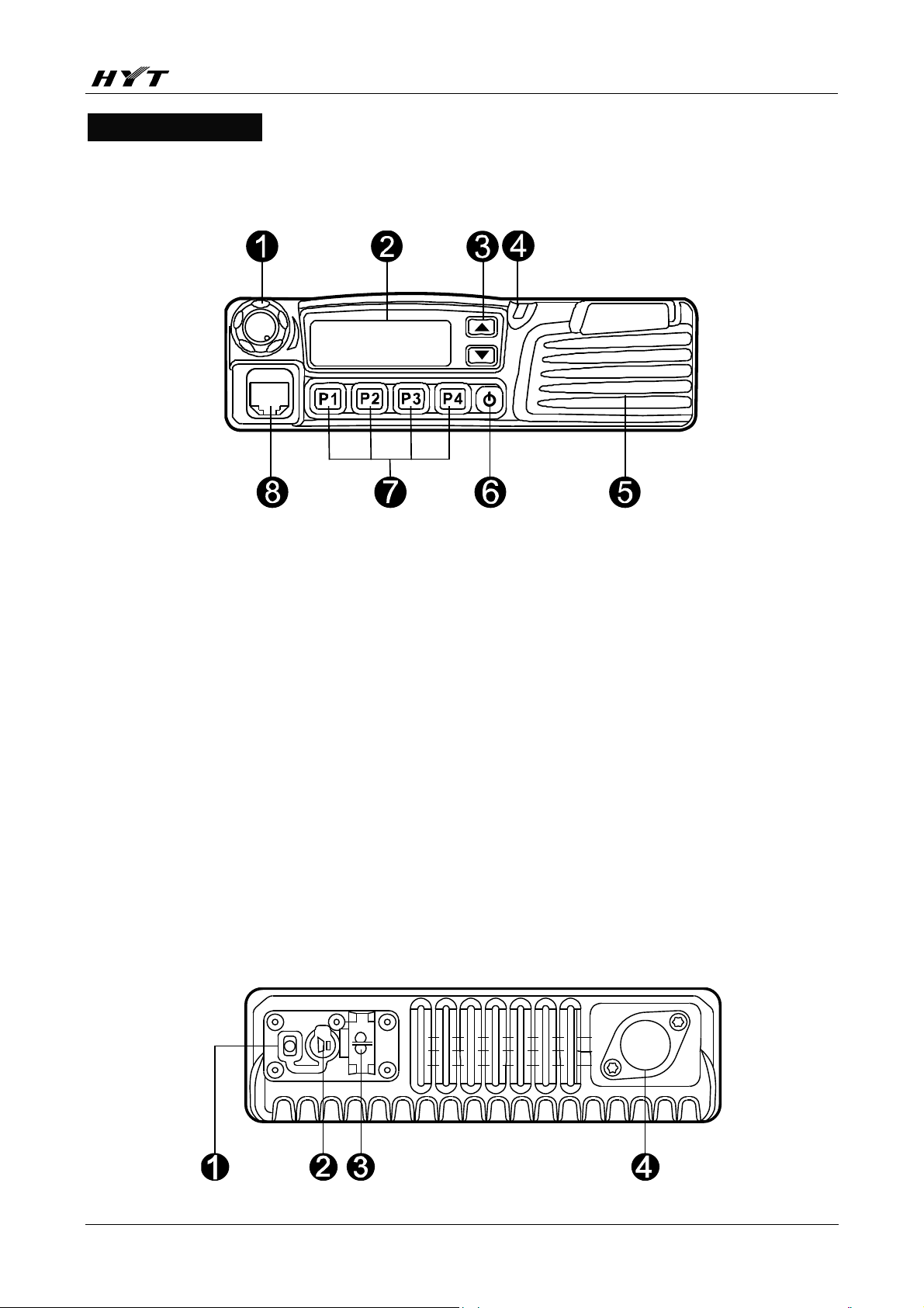
Radio Overview
Front Panel View
TM-
① Volume Control Knob
Rotate the knob clockwise to increase the volume and counter-clockwise to decrease the volume.
② LCD
Please refer to section LCD Display.
③ Programmable Function Keys ▲ / ▼
Your local dealer can program these keys with various auxiliary functions.
Please refer to section Programmable Function Keys.
④ LED Indicator
⑤ Speaker
⑥ Power Switch
⑦ Programmable Function Keys P1 / P2 / P3 / P4
Your local dealer can programmed these keys with various auxiliary functions.
Please refer to section Programmable Function Keys.
⑧ Microphone Jack
Plug the microphone into the jack.
Rear Panel View
3
Page 5

TM-
① 15 Pin Connector (for external expansion)
② External Speaker Jack
Used to connect an external speaker with a 3.5 mm plug. Refer to Test Cable for Speaker Output in Tuning Description for
details.
③ Power Inlet
Use HYT-authorized DC power cord to inlet 13.6 V DC power.
④ Antenna Connector
Used to connect an external antenna.
Microphone
LED Indicator
Light green Receiving
Flash orange Receiving 5-Tone call
Light orange Transmitting call
LCD Display
Indicator Description
Light red Transmitting
Figure 1 LCD Panel
4
Page 6

Indicator Description
1. Display zone / channel number.
2. Display channel label
3. Display DTMF digit
4. Display channel Frequency
5. Display menu, setting items, etc.
Lo Display when the transmitting power is low.
The icon appears if any of the following conditions occurs:
1. Monitor status activated by pressing the Monitor key, and the channel
is initialized to Monitor Squelch.
2. Monitor status activated by a call or decoding, i.e., auto reset mode.
3. Monitor status activated by Force Monitor.
4. Carrier squelch mode under Rx Squelch.
5. Monitor status with authorization request.
TM-
The icon appears when speaker is unmated.
Appears when scan mode is active.
Appears during the auto reset time.
Appears when DTMF Keypad mode is enabled.
Appears when scrambler function is enabled.
Appears when compander function is enabled.
Appears when the selected channel is busy.
Appears when scan pauses on a priority channel. P•standards for
Priority Channel 1, P. standards for Priority Channel 2, and P: standards
for Priority Channels 1& 2.
5
Page 7

Programmable Function Keys
[P1]-[P4], [▲ ]/ [▼ ] can be programmed with the following auxiliary functions:
1. None
2. CH Up
3. CH Down
4. Zone Up
5. Zone Down
6. Monitor/ Cancel Call
7. Cancel Call
8. Display Channel Alias
9. Display Freqency
10. Display Mode Switch
11. User Selectable Tone
12. Adjust Power Level
13. Scan
14. Nuisance Temporary Delete
15. Reverse
16. Talk Around
17. Adjust Squelch Level
18. Home Channel
19. Public Adress
20. Scrambler
21. Compander
22. AUX A
23. AUX B
24. Emergency
25. Call Forward
26. Wisper
27. Lone-Worker
28. Contact List
29. Status List
30. Channel Shortcut Button
31. Missed Calls
32. Received Calls
33. Keypad Mode
34. Menu
35. Call 1
36. Call 2
37. Call 3
38. Call 4
39. Call 5
TM-
6
Page 8
Software Specifications
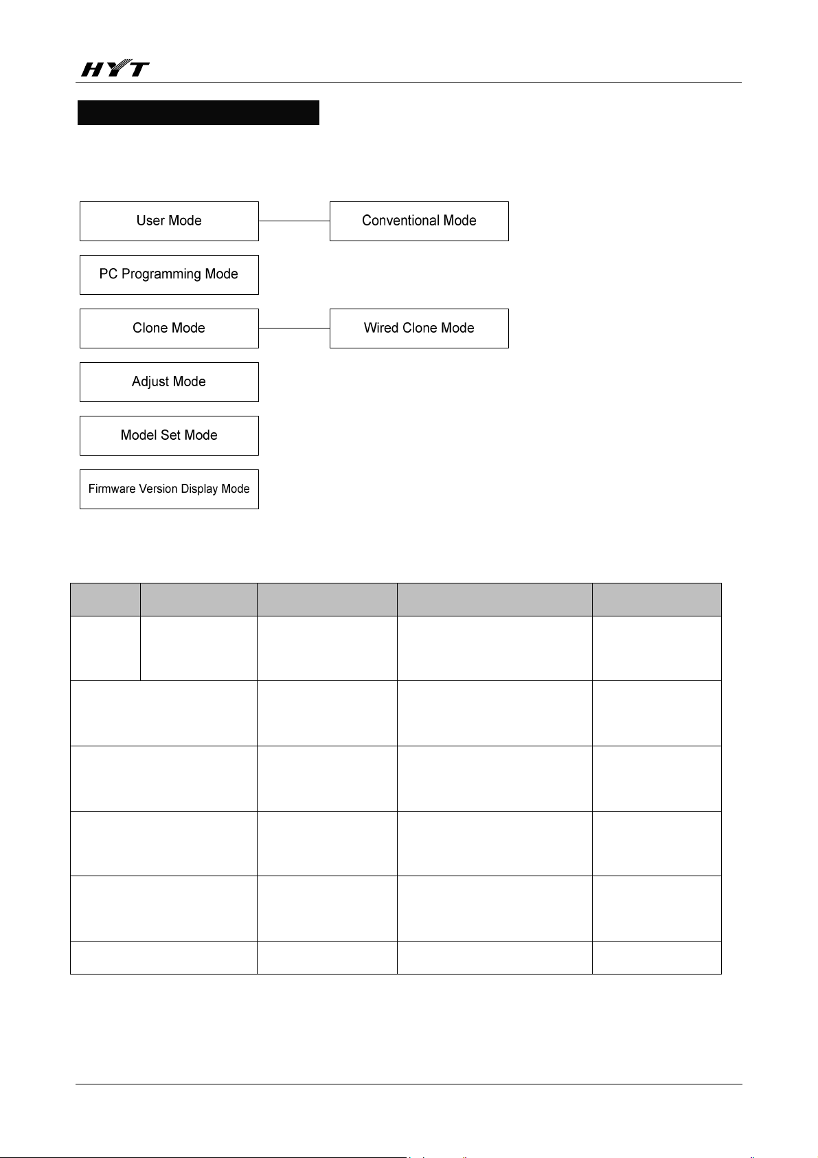
Radio Modes
1. Frame of Radio Modes
TM-
2. Keypad Entry for Mode Startup
MODE Main Menu Display/Sub Menu Operation Remarks
USER
MODE
ADJUST MODE ----------------------------
Model Set Mode ----------------------------
Firmware Version Display
Mode
Wired Clone Mode ----------------------------
Conventional
Mode
Turn on the radio to enter
---------------------------Conventional Mode
Press and hold [P1] to turn the
radio on.
Press and hold [P2] to turn the
radio on.
While holding down [P4] key,
---------------------------turn on the radio
While holding down [P3] key,
turn on the radio
PC Programming Mode ---------------------------- Receive commands from PC
Note: When power-on password is enabled, you must input the correct password before you can enter User Mode.
You can input password through the keypad and press [#] to clear.
7
Page 9

TM-
3. Error Information and Measures in User Mode
The radio self-checks when power on. If no error is detected, the radio enters conventional mode. While the radio will
sound alert once any error is checked.
Error information and measures:
No. Error Information LCD Display Measures
1 Stun status Stun Re-program.
Re-program with programming software of right
2 Data and Firmware Version mismatch No Data
version.
4. Firmware Version Display Mode
Turn the radio on while holding down [P4] to enter Firmware Version Display Mode, the firmware version will be displayed
on the LCD.
Release [P4] to enter User Mode.
5. PC Programming Mode
Connect the radio with a PC by programming cable. If data is written to the radio from PC, it can be programmed into the
EEPROM. Data programming is accessible by programming software.
When data is written to the radio from PC, “PROGRAM”appears on the LCD. LED glows green when data is written to the
radio and red when data is read from the radio. Radio will restart automatically when programming is completed.
6. Wired Clone Mode
Data can be transmitted from radio to radio by wired cloning.
(1) Turn on the source radio while holding down [P3] simultaneously, the radio enters Clone Mode with “CLONE”on
the LCD, or enters User Mode if Clone Mode is disabled by your dealer.
(2) Press [P3] to toggle between Dealer Clone and Factory Clone Mode. “DEACLONE”or “FACCLONE”appears on
the display when the corresponding mode is selected. The radio restores the original display after 5 seconds.
Unlike Factory Clone Mode, adjustment settings and embedded messages are not covered in Dealer Clone Mode.
Dealer Clone Mode is the default mode.
(3) Connect the two radios by cloning cable, then turn on the target radio.
(4) Press [P4] to start cloning, the LED of source radio glows red and that of target radio glows green during cloning.
“PROGRAM”is also displayed on the target radio. “END”appears on the source radio when cloning is completed
and the target radio enters user mode.
(5) Press [P4] to return to Clone Mode. “CLONE”appears on the source radio. Repeat the above steps to continue
wired cloning.
Note: Cloning is available only when both radios are in the same mode.
7. Panel Tuning Mode
The radio is tuned in this mode. Operations are as follows:
(1) Press [P1] to turn on the radio and enter tuning mode.
8
Page 10
TM-
(2) Select the item with [Up]/[Down] keys. Press [P4] to enter the selected sub-item.
(3) Press [P4] to enter the sub-item and tune the data with [Up]/[Down] keys. Then press [P4] to save the data and
enter the next sub-item. Press [P1] to go back to the previous item without saving the data.
8. Model Set Mode
(1) Press [P2] to turn the radio on. The radio enters Model Set Mode. The frequency band appears on the LCD.
(2) Press [Up]/[Down] to choose right frequency band.
(3) Press [P4] to confirm. LED glows orange and ”WAIT”appears on the LCD; then the radio enters User Mode after
reset.
Notes:
1. Once [P4] key is pressed to set the new model, the previously stored channel data (frequency, CTCSS/CDCSS,
channel function settings) will be cleared, and part of functions also change. Therefore, do not make this operation unless
it’s necessary.
2. Initialization Data Table and frequency range (FL: lowest frequency- FH: highest frequency -FC: center frequency) of
different models are shown in the following table.
Model RX/TX 1 ( C ) 2 ( L ) 3 ( H ) 4 5 6 7 8
0 RX(MHz) 155.15 136.15 173.85 145.55 164.5 155 155.2 155.4
(V) TX(MHz) 155 136 174 145.5 164.5 155 155.2 155.4
1 RX(MHz) 435.15 400.15 469.85 417.55 452.5 435 435.2 435.4
(U1) TX(MHz) 435 400 470 417.5 452.5 435 435.2 435.4
2 RX(MHz) 475.15 450.15 499.85 462.55 487.5 475 475.2 475.4
(U2) TX(MHz) 475 450 500 462.5 487.5 475 475.2 475.4
3 RX(MHz) 495.15 470.15 519.85 482.55 507.5 495 495.2 495.4
(U3) TX(MHz) 495 470 520 482.5 507.5 495 495.2 495.4
4 RX(MHz) 375.15 350.15 399.85 362.55 387.5 375 375.2 375.4
(U4) TX(MHz) 375 350 400 362.5 387.5 375 375.2 375.4
5 RX(MHz) 455.15 440.15 469.85 447.55 462.55 455 455.2 455.4
(U5) TX(MHz) 455 440 470 447.5 462.5 455 455.2 455.4
6 RX(MHz) 503.15 480.15 525.85 491.55 514.55 503 503.2 503.4
(U6) TX(MHz) 503 480 526 491.5 514.5 503 503.2 503.4
7 RX(MHz) 340.15 330.15 349.85 335.05 345.05 340 340.2 340.4
(U7) TX(MHz) 340 330 350 335 345 340 340.2 340.4
TM600V: 136-174MHz
TM600U1: 400-470MHz
TM600U2: 450-500MHz
TM600U3: 470-520MHz
TM600U4: 350-400MHz
TM600U5: 440-470MHz
TM600U6 (for Taiwan only): 480-526MHz
TM600U7: 330-350MHz
9
Page 11

TM-
CH
CTCSS Rx None None None CTS67.0HZ D023 CTS67.0HZ DI423 None
CDCSS Tx None None None CTS67.0HZ D023 CTS67.0HZ DI423 None
PWR Tx L L L L L L L L
CH CH 1 CH 2 CH 3 CH 4 CH 5 CH 6 CH 7 CH 8
NAME Wide Wide Wide Wide Wide Wide Wide Wide
1 2 3
4
5 6 7 8
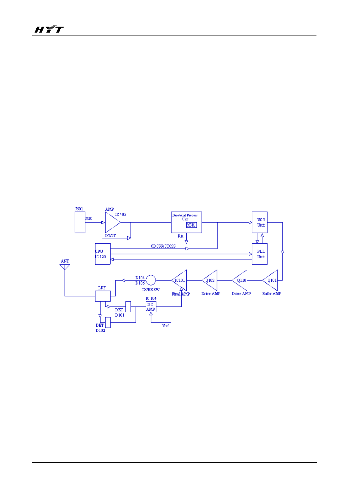
Circuit Description
1. Frequency Configuration
The receiver utilizes double conversion superheterodyne. The first IF is 49.95MHz and the second is 450KHz. The first
local oscillator signal is supplied by the PLL circuit; and the second (50.4MHz) is generated from the frequency tripling of
TCXO (16.8MHz). The PLL circuit generates the frequencies required for transmission. (See figure 1).
Frequency Range VHF: 136MHz - 174MHz
UHF: 400MHz - 470MHz 450MHz - 500MHz
470MHz - 520MHz 350MHz - 400MHz
440MHz - 470MHz 480MHz - 526MHz
330MHz - 350MHz
2. Receiver Circuit
The receiver circuit is shown as figure 1.
Figure 1 Receiver Circuit
2.1 High Frequency Bandpass Amplifier Circuit
It consists of BPF, RF amplifier (Q111) and BPF (D110 and D111). The range of bandpass frequency is the frequency
range of the radio itself. The signal is filtered by the BPF to eliminate unwanted signals before going to the first mixer.
2.2 First Mixer
The signal from BPF is mixed with the first local oscillator signal from PLL circuit at the first mixer (D112) to become a
49.95MHz first IF signal. The first IF signal is then fed through the crystal filter (IF200) to further remove spurious signals.
2.3 IF Amplifier
The first IF signal is amplified by Q113 and then enters IC102 (TA31136FN), where the signal is mixed again with the
10
Page 12
TM-
second local oscillator signal (50.4MHz) to become a 450KHz second IF signal. The second IF signal is then fed through a
ceramic filter (N: CF202; W: CF203) to eliminate unwanted signals. The resulting signal then is detected by IC102 and
output from Pin 9 as audio signals.
2.4 Audio Amplifier
The audio signal obtained from IC102 is amplified and filtered by IC402 before being amplified by IC401 (the received
signalling is separated and input into CPU for decoding). The processed signalling passes through Q406 (AF MUTE) and
is amplified by IC405. The amplified signal is fed to K301 controlling the volume and Q511 controlling SP MUTE on the
front panel before entering audio amplifier (IC511). The output audio signal drives the speaker.
2.5 Squelch Open
Part of the audio signals output from IC102 passes through IC102 Pin8 and is amplified by IC102 again, then is filtered
and rectified to produce an SQL level. The SQL level is compared with the existing reference level in CPU (IC502) to
generate a level to control AF MUTE and SP MUTE, which determines whether to output sounds from the speaker by
controlling Q406 and Q511.
3. Transmitter Circuit
The transmitter circuit is composed of the MIC circuit, modulation circuit, RF driver, final-stage power amplification circuit
and APC circuit.
Figure 2 Transmitter Circuit
3.1 MIC and Modulation Circuit
The audio signal from MIC is amplified by IC405 before being pre-emphasized and encoded by IC401. The output audio
signal is added into signalling and then is fed through VCO for modulation.
3.2 RF Driver and Final-Stage Power Amplification Circuit
The Tx-RF signal output from Q703 in the VCO circuit is amplified by Q101, drivers Q110 and Q109. The amplified signal
is then fed to IC101 (final-stage amplifier) and passes through LPF before reaching the antenna.
3.3 APC
The APC circuit stabilizes the output power at a predetermined level. D101 and D102 transform the signal from the
detector to DC voltage, which is then compared with the reference voltage from CPU in IC104 to output a DC voltage. The
DC voltage controls the output power by controlling the grid of IC101.
11
Page 13
TM-
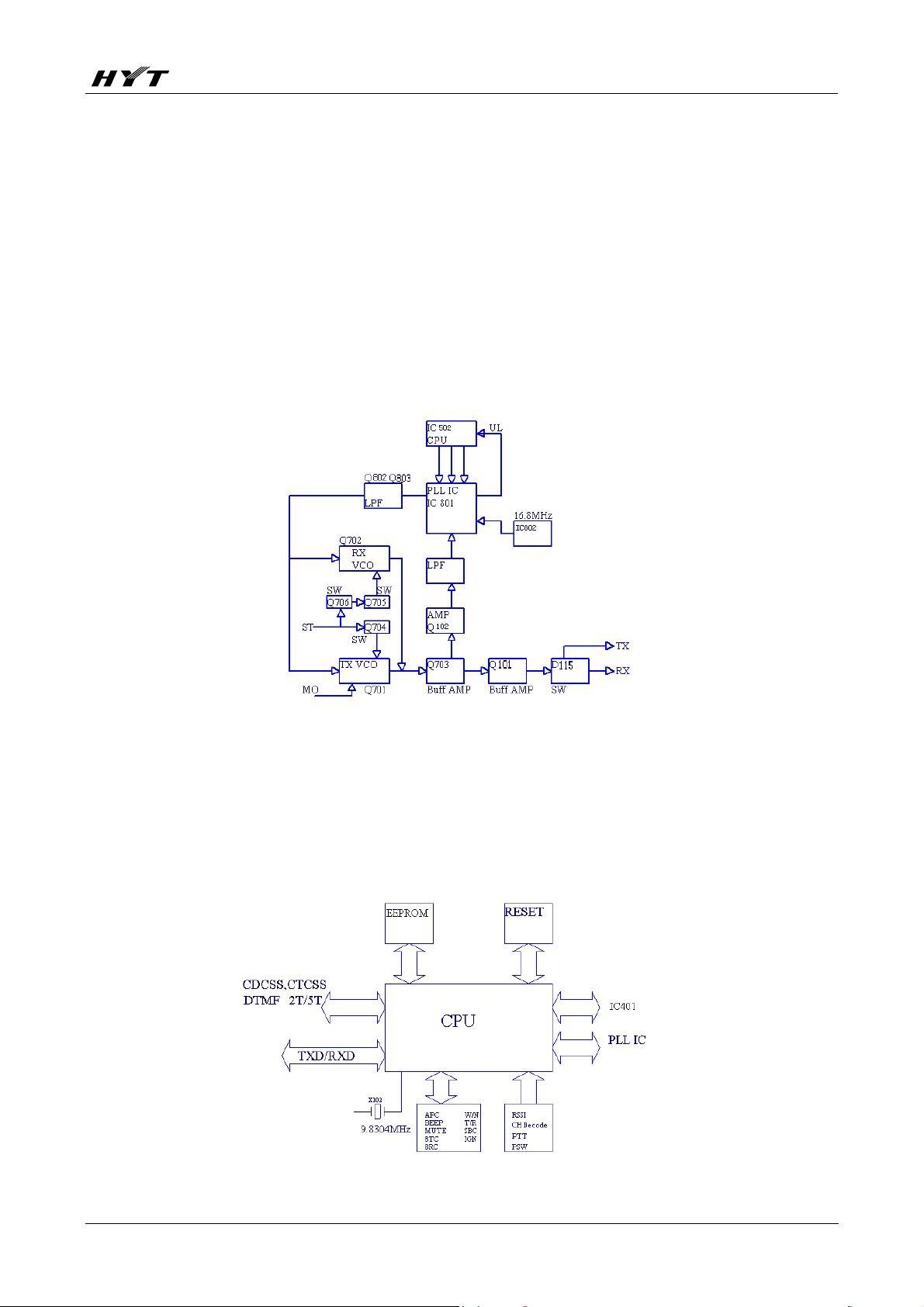
4. PLL Circuit
The frequencies of receiving the first local oscillator signal and transmitting signal are generated by the PLL circuit. The
PLL circuit consists of Tx frequency oscillator (Q701), Rx frequency oscillator (Q702), buffer amplifier (Q703), RF amplifier
(Q102), PLL IC (IC801), LPF and Tx/Rx VCO control switch (Q704, Q706).
In transmit mode, IC120 transmits the frequency data to PLL IC. Q704 is turned on to activate Tx VCO. The output signal
is amplified by Q703 and Q102, and then divided by PLL IC into 2.5KHz, 5KHz or 6.25KHz signals. The divided signal is
compared with the 2.5KHz, 5KHz or 6.25KHz reference signal from a 16.8MHz crystal oscillator (2.5 PPM frequency
stability) in the phase comparator. The frequency control voltage output from the phase comparator issent to Tx VCO after
passing through LPF (Q802, Q803). In the meantime, the modulation signal (Tx) is passed to Tx VCO for frequency
modulation.
The working principle in receive mode is similar to that in transmit mode.
Figure 3
5. Control Circuit
The control circuit is composed of CPU, reset IC and power supply control circuit.
5.1 CPU
IC502 (CPU) operates at 9.8304MHz. CPU controls the data transmission among E2PROM (IC501), Rx circuit, Tx circuit,
control circuit, display circuit and peripheral circuits.
Figure 4 Control Circuit
12
Page 14
TM-
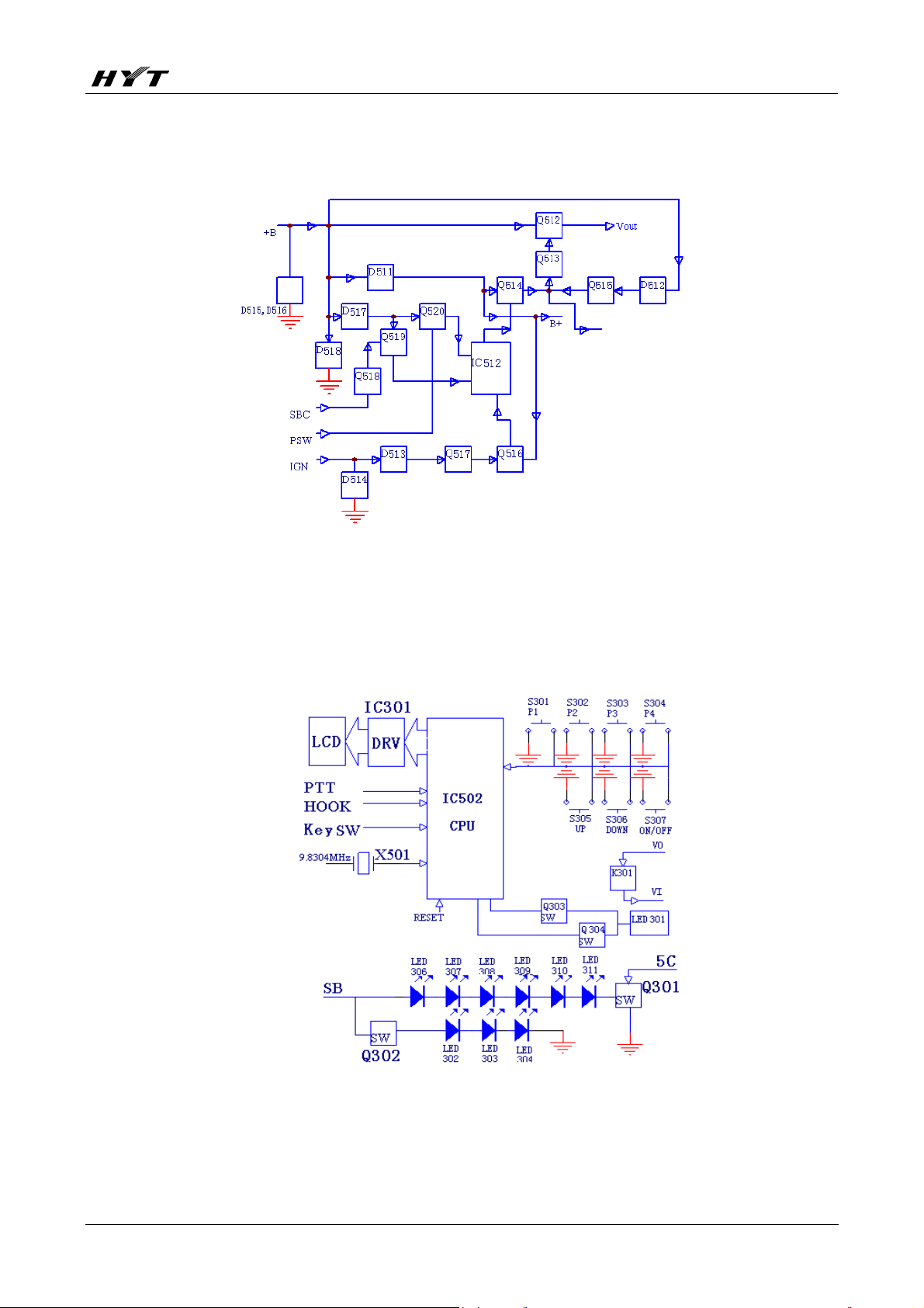
5.2 Power Supply
+B supplies power for the radio. D135 and D137 are over-voltage protection diodes. Power-on/off can be controlled via
the software.
Figure 5 Power Supply Circuit
Vout provides power for IC601, IC602 and IC803, which produces 8V, 5V, 3.3V voltage for the circuit.
6. Display Circuit
The display circuit is comprised of CPU (IC502), LCD, LED and other components. The radio can be manually operated
through P1 / P2 / P3 / P4 and ▲ / ▼ keys. Relevant channel information is displayed on the 15-segment LCD in
alphanumeric form.
Figure 6 Display Circuit
13
Page 15
TM-
Semiconductor Data
1. Positive Voltage Regulator: TA7805F (POWER unit IC602) and TA7808S (POWER unit 601).
2. EEPROM: AT24C256N10SI2.7 (CPU unit IC501)
2.1 Pin Function
Pin No. Name I/O Function
1~3 A0~A2 I Address input
4 GND GND
5 SDA I/O Serial data
6 SCL Serial clock input
7 TEST Test
8 VCC +5V.
3. Audio Processor: AK2346 (AFPwr Unit IC404)
3.1 Pin Function
Pin No. Name I/O Function
1 AGNDIN I Analog ground input
2 AGND O Analog ground output
3 TxIN I Tx audio signal input
4 TxINO O TxA1 feedback output
5 LIMLV I Limit level tuning
6 EXTLIMIN I External signal input pin for pre-limiter circuit.
7 MOD O Modulated Tx signal output
8 VSS GND.
9 TCLK O Clock output pin for MSK transmission data.
10 TDATA I MSK transmission data input
Delay data is latched with the TCLK rising edge.
11 DI/O I/O Serial data input and output
Memory setting data during inputting; MSK receiving signal during outputting
12 RDF/FC O MSK signal output of receiving flag and frame detection signal
13 SCLK I I/O clock input of serial data
14 DIR I Serial data I/O control
15 XOUT I Crystal oscillator input
16 XIN I/O Crystal oscillator input and output
17 VDD Positive power supply
18 EXPOUT O Output signal after audio processing
19 RxAFIN I Rx audio signal input
20 RxAF O Rx audio signal output
21 RxLPFO O Rx LPF output
22 RxINO O RxA1 feedback output
23 RxIN I Demodulated Rx signal input
24 TEST I Test register control input
4. Audio Power Amplifier: TDA7297D (AFPwr unit IC511)
Pin Function
14
Page 16
Pin No. Name I/O Function
1 PW GND Power ground 1
2 OUT1+ O Output 1+
3 N.C
4 N.C
5 OUT1- O Output 1-
6 VCC I Supply voltage
7 IN1 I Input 1
8 MUT I Operation switch
9 STAND-BY I Operation switch
10 PW GND Power ground 2
11 PW GND Power ground 3
12 N.C
13 SGND Signal ground
14 IN2 I Input 2
15 VCC I Supply voltage
16 OUT2- O Output 217 N.C
18 N.C
19 OUT2+ O Output 2+
20 PW GND Power ground
5. LCD Driver: PCF8576DH (Display unit IC501)
Pin No. Name I/O Function
1 N.C.
2~7 S34~S39 O Output LCD.
8~9
10 SDA I/O Input/output I2C bus serial data
11 SCL O Output I2C bus clock
12 SYNC I N.C.
13 CLK I/O N.C.
14 V
15 OSC I Internal quartz crystal oscillator enable input
16~18 A0~A2 I Address line
19 SA0 I I2C bus sub-address bit 0
20 Vss GND
21 V
22~24 N.C.
25~28 BP0~BP3 O LCD base panel output
29~32 S0~S4 O Output LCD
33 N.C. .
34~47 S5~S18 O Output LCD
48 N.C.
49、50 S19、S20 O Output LCD
51~64 S21~S34 O Output LCD
N.C.
DD
LCD
Power supply
N.C
TM-
15
Page 17
TM-
6. Amplifier: TA75W558FU (AFPr unit IC404), TC75W51FU (AFPr unit IC402, AFPr unit IC405, AFPr unit IC403),
TA75S01F (RF unit IC1037), TA75W01FU (RF unit IC404).
7. IF Detector: TA31136FN (RF unit IC102).
8. Dual D-type trigger: TC4013BF (AFPwr unit IC512).
9. RF PLL Frequency Synthesizer: MB15A02 (PLL unit IC801).
10. CPU: SCM M3062LFGPGP (CPU unit IC502)
10.1 Pin Function
PIN No. Port Name Pin Name I/O Function
1 P94/DA1 APC O Modulated sensitivity output
2 P93/DA0 DTMF O DTMF/2-Tone/5-Tone/BEEP output
3 P92/ TB2in 2TN/5TN I 2-Tone/5-Tone decode pulse input
4 P91 AFDIO I/O AK2346 DATA I/O(SDAT)
5 P90 AFSCLK O AK2346 serial clock (SCLK)
6 BYTE BYTE I +5V(5C)
7 CNVSS CNVSS I GND (ground via 0 resistance)
8 P87 PA O MIC PAswitch control,PA: H
9 P86 HMBL O Microphone backlight control
10 RESET RESET I Reset
11 XOUT XOUT O Clock output
12 VSS VSS I GND
13 XIN XIN I Clock input
14 VCC VCC I +5V
15 P85/NMI NMI I NMI (usually not used)
16 P84/INT2 AFRDF I Baseband chip MSK receive detect (RDF/FD)
17 P83/INT1 DTMFSTD I Not used (left open)
18 P82/INT0 AUX1 I/O Optional circuit board port 1(input)(renamed AUX1)
19 P81/TA4in SBC SB Power switch control,H: off,L: on
20 P80/TA4out CTC_OUT O CDCSS Balance
21 P77/TA3in SPMUTE O SP Mute,Mute: H
22 P76/TA3out CTC_PLL O CTCSS/CDCSS modulation output
23 P75/TA2in EMICC O External Mic control,External Mic: H (now NC)
24 P74/TA2out AFTDATA O Baseband chip MSK serial data (TDATA)
25 P73/TA1in AFTCLK I Baseband chip MSK serial clock (TCLK)
26 P72/TA1out AFDIR O Baseband chip I/O control pin (DIR)
27 P71/RxD2 RxD2 I Not used
28 P70/TxD2 TxD2 I Not used
29 P67/TxD1 TxD1 O Serial data output,PTT ON: L
30 P66/RxD1 RxD1 I Microphone HOOK input/serial data input,ON: L
31 P65 AUX4 I/O AUX4— — optional circuit board port 5 (output)
32 P64 AUX5 I/O AUX5— — optional circuit board port 6 (output)
33 P63 TxD2 O Acc comm0 (serial data output)
34 P62 RxD2 I Acc comm0 (serial data input)
35 P61 MICDAT I/O Microphone key code data input/output
16
Page 18
TM-
36 P60 AUX2 I/O AUX2— — optional circuit board port 2 (input)
37 P57 RDY I Pull Up
38 P56 NC Not used (left open)
39 P55 HOLD Not used (left open)(for recording)
40 P54 NC Not used (left open)
41 P53 NC Not used (left open)
42 P52 RD O External expansion, read(Not used)
43 P51 NC Not used (left open)
44 P50 WR O External expansion, write(Not used)
45 P47 HNC O Horn alert control,ON: H,(Not used)
46 P46 SHIFT O Clock beat frequency,ON: H
47 P45 W/N O W/N switch,W: L,(change W to H)
48 P44 CS0 O NC (left open)
49 P43 MicMute O Mic mute,Mute: L,(change to H active)
50 P42 KEYBL O Keypad backlight control,ON: H, (NC)
51 P41 UP/LED4 O UP/LED4
52 P40 LED6 O LED6
53 P37 LCDCI/LED3 I/O LCD Driver CI PIN /LED3
54 P36 DOWN/LED5 O DOWN/LED5
55 P35 LCDCL/LED2 O LCD,Driver CL,PIN/LED2
56 P34 LCDBL/LED0 O LCD,Driver BL,PIN/LED0
57 P33 LED7 O LED7
58 P32 LCDCE/LED1 O LCD Driver CE PIN/LED1
59 P31 RLED O Red indicator
60 VCC VCC I +5V
61 P30 GLED O Green indicator
62 VSS VSS I GND
.63~66 A7~A4 A7~A4 I Not used (left open)
67 P23 PLLDAT O PLL data output
68 P22 PLLCLK O PLL clock output
69 P21 SLED O Scan status indicator
70 P20 PLED O High/low power indicator
71 P17 8RC O 8R power control,Rx: H
72 P16 8TC O 8T power control,Tx: H
73 P15 Rx O Tx/Rx VCO switch,Rx: L
74 P14 EEPDAT I/O EEPROM data input/output
75 P13 EEPCLK O EEPROM clock output
76 P12 PLLUL I PLL unlock detect,Unlock: L
77 P11 PLLSTB O PLL strobe output,Lock: L
78 P10 AFMUTE O Receive AF MUTE,Mute: H
79 P07 /IGN I Ignition sense input,H: off;L: on
80 P06 PWR I PWR key input,ON: L
17
Page 19
TM-
81 P05 TYPE I TM-610/TM-610 Selection input,H: TM-610; L: TM82 P04 NC I Left open
83 P03 P4 I P4 input,ON: L (external pull-up resistor)
84 P02 P3 I P3 input,ON: L (external pull-up resistor)
85 P01 P2 I P2 input,ON: L (external pull-up resistor)
86 P00 P1 I P1 input,ON: L (external pull-up resistor)
87 AN7 Not used (left open)
88 AN6 Volume I Volume Tuning input
89 AN5 DTMF soft decode preserve
90 AN4 DTMF soft decode preserve
91 AN3 Temperature I Temperature data input
92 AN2 RSSI I RSSI input
93 AN1 SQL I SQL analog input
94 AVss AVss GND
95 AN0 TI I CTCSS/CDCSS signal input
96 VREF VREF I Reference voltage input
97 AVCC AVCC I +5V
98 P97/Sin4 AUX3 I/O Optional circuit board port 3 (INPUT)
99 P96/Sout4 AUX6 I/O Optional circuit board port 6 (OUTPUT)
100 P95/Clk4 APCO I/O Audio amplifer control port
Component Description
1. Tx-Rx Unit
Ref. No. Part Name Type Description
IC101 IC Power module Power module
IC501 IC AT2408N12.5S EROM
IC401 IC AK2346 Audio processor
IC404 IC TA75W558FU Dual operational amplifier
IC403 IC TC75W51FU Dual operational amplifier
IC803 IC XC62FP3302P Positive voltage regulator
IC602 IC TA7805F Positive voltage regulator
IC103 IC TA75S01F Single operational amplifier
IC104 IC TA75W01FU Dual operational amplifier
IC102 IC TA31136FN IF detector
IC502 IC M30624FCPGP#U5C CPU
IC121 IC BU4066BCFV Quad analog switch
IC122 IC LC73872M DTMF Rx circuit
IC125 IC M62364FP D/A converter with buffer amplifiers
IC126 IC TDA8561Q Power amplification
IC127 IC TC4013BF Dual D-type trigger
IC301 IC PCF8576DH LCD driver
18
Page 20
TM-
TM-610 Parts List 1
Tx-Rx Unit (UHF)
No. Material No. Description Qty. Ref. No. Print No. Remarks
1 3001050000000 Chip resistor 0402 0Ω J 1/16W 1 C404 B5E
2 3001050000000 Chip resistor 0402 0Ω J 1/16W 1 R106 T2B
3 3001050000000 Chip resistor 0402 0Ω J 1/16W 1 R110 T3B
4 3001050000000 Chip resistor 0402 0Ω J 1/16W 1 R419 B5E
5 3001050000000 Chip resistor 0402 0Ω J 1/16W 1 R448 B5F
6 3001050000000 Chip resistor 0402 0Ω J 1/16W 1 R451 B5F
7 3001050000000 Chip resistor 0402 0Ω J 1/16W 1 R455 T5F
8 3001050000000 Chip resistor 0402 0Ω J 1/16W 1 R457 B5C
9 3001050000000 Chip resistor 0402 0Ω J 1/16W 1 R480 T4B
10 3001050000000 Chip resistor 0402 0Ω J 1/16W 1 R483 B4B
11 3001050000000 Chip resistor 0402 0Ω J 1/16W 1 R485 T4F
12 3001050000000 Chip resistor 0402 0Ω J 1/16W 1 R501 T4C
13 3001050000000 Chip resistor 0402 0Ω J 1/16W 1 R509 T5F
14 3001050000000 Chip resistor 0402 0Ω J 1/16W 1 R510 T4C
15 3001050000000 Chip resistor 0402 0Ω J 1/16W 1 R513 T4C
16 3001050000000 Chip resistor 0402 0Ω J 1/16W 1 R518 T5E
17 3001050000000 Chip resistor 0402 0Ω J 1/16W 1 R520 T5E
18 3001050000000 Chip resistor 0402 0Ω J 1/16W 1 R521 T5E
19 3001050000000 Chip resistor 0402 0Ω J 1/16W 1 R522 T5E
20 3001050000000 Chip resistor 0402 0Ω J 1/16W 1 R591 T5F
21 3001050000000 Chip resistor 0402 0Ω J 1/16W 1 R600 T5F
22 3001050000000 Chip resistor 0402 0Ω J 1/16W 1 R605 B2F
23 3001050000000 Chip resistor 0402 0Ω J 1/16W 1 R608 T5F
24 3001050000000 Chip resistor 0402 0Ω J 1/16W 1 R611 T4C
25 3001050000000 Chip resistor 0402 0Ω J 1/16W 1 R620 T5F
26 3001050000000 Chip resistor 0402 0Ω J 1/16W 1 R625 T5F
27 3001050000000 Chip resistor 0402 0Ω J 1/16W 1 R627 T4C
28 3001050000000 Chip resistor 0402 0Ω J 1/16W 1 R154 T4A U1:400-470MHz
29 3001053030010 Chip resistor 0402 30KΩ J 1/1 1 U2:450-500MHz
30 3001050000000 Chip resistor 0402 0Ω J 1/16W 1 R153 T4A U1:400-470MHz
31 3001053320000 Chip resistor 0402 3.3KΩ J 1/ 1 U2:450-500MHz
32 3001051010000 Chip resistor 0402 100Ω J 1/1 1 R146 T2D
33 3001051010000 Chip resistor 0402 100Ω J 1/1 1 R197 T3A
34 3001051020010 Chip resistor 0402 1KΩ J 1/16 1 R145 B3A
35 3001051020010 Chip resistor 0402 1KΩ J 1/16 1 R200 T4A
36 3001051020010 Chip resistor 0402 1KΩ J 1/16 1 R439 B5E
37 3001051020010 Chip resistor 0402 1KΩ J 1/16 1 R453 B4F
38 3001051020010 Chip resistor 0402 1KΩ J 1/16 1 R476 B5B
39 3001051020010 Chip resistor 0402 1KΩ J 1/16 1 R503 T4C
40 3001051020010 Chip resistor 0402 1KΩ J 1/16 1 R504 T4C
19
Page 21

TM-
41 3001051020010 Chip resistor 0402 1KΩ J 1/16 1 R505 T3D
42 3001051020010 Chip resistor 0402 1KΩ J 1/16 1 R506 T3D
43 3001051020010 Chip resistor 0402 1KΩ J 1/16 1 R609 T4D
44 3001051020010 Chip resistor 0402 1KΩ J 1/16 1 R610 T4D
45 3001051020010 Chip resistor 0402 1KΩ J 1/16 1 R612 T4D
46 3001051020010 Chip resistor 0402 1KΩ J 1/16 1 R632 T4D
47 3001051020010 Chip resistor 0402 1KΩ J 1/16 1 R802 T3D
48 3001051020010 Chip resistor 0402 1KΩ J 1/16 1 R823 T3D
49 3001051020010 Chip resistor 0402 1KΩ J 1/16 1 R824 T3D
50 3001051020010 Chip resistor 0402 1KΩ J 1/16 1 R825 T3D
51 3001051020010 Chip resistor 0402 1KΩ J 1/16 1 R826 T3D
52 3001051030000 Chip resistor 0402 10KΩ J 1/1 1 R112 T2B
53 3001051030000 Chip resistor 0402 10KΩ J 1/1 1 R198 T3A
54 3001051030000 Chip resistor 0402 10KΩ J 1/1 1 R402 B4E
55 3001051030000 Chip resistor 0402 10KΩ J 1/1 1 R403 B4E
56 3001051030000 Chip resistor 0402 10KΩ J 1/1 1 R904 B5C
57 3001051030000 Chip resistor 0402 10KΩ J 1/1 1 R423 B4E
58 3001051030000 Chip resistor 0402 10KΩ J 1/1 1 R424 B4E
59 3001051030000 Chip resistor 0402 10KΩ J 1/1 1 R428 B4D
60 3001051030000 Chip resistor 0402 10KΩ J 1/1 1 R449 B5F
61 3001051030000 Chip resistor 0402 10KΩ J 1/1 1 R450 B5F
62 3001051030000 Chip resistor 0402 10KΩ J 1/1 1 R464 B4C
63 3001051030000 Chip resistor 0402 10KΩ J 1/1 1 R470 B5B
64 3001051030000 Chip resistor 0402 10KΩ J 1/1 1 R472 B5B
65 3001051030000 Chip resistor 0402 10KΩ J 1/1 1 R477 B5B
66 3001051030000 Chip resistor 0402 10KΩ J 1/1 1 R804 T2D
67 3001051030000 Chip resistor 0402 10KΩ J 1/1 1 R902 B5C
68 3001051030000 Chip resistor 0402 10KΩ J 1/1 1 R418 B5E U1:400-470MHz
69 3001051830000 Chip resistor 0402 18KΩ J 1/1 1 U2:450-500MHz
70 3001051040010 Chip resistor 0402 100KΩ J 1/ 1 R104 T2B
71 3001051040010 Chip resistor 0402 100KΩ J 1/ 1 R107 T3B
72 3001051040010 Chip resistor 0402 100KΩ J 1/ 1 R115 T3B
73 3001051040010 Chip resistor 0402 100KΩ J 1/ 1 R116 T3B
74 3001051040010 Chip resistor 0402 100KΩ J 1/ 1 R148 T2D
75 3001051040010 Chip resistor 0402 100KΩ J 1/ 1 R149 T3A
76 3001051040010 Chip resistor 0402 100KΩ J 1/ 1 R180 T2D
77 3001051040010 Chip resistor 0402 100KΩ J 1/ 1 R427 B4D
78 3001051040010 Chip resistor 0402 100KΩ J 1/ 1 R467 B5B
79 3001051040010 Chip resistor 0402 100KΩ J 1/ 1 R468 B5B
80 3001051040010 Chip resistor 0402 100KΩ J 1/ 1 R514 T4E
81 3001051040010 Chip resistor 0402 100KΩ J 1/ 1 R565 T5G
82 3001051040010 Chip resistor 0402 100KΩ J 1/ 1 R566 T5G
83 3001051040010 Chip resistor 0402 100KΩ J 1/ 1 R801 T3D
84 3001051040010 Chip resistor 0402 100KΩ J 1/ 1 R806 T3C
85 3001051040010 Chip resistor 0402 100KΩ J 1/ 1 R820 T3F
20
Page 22

TM-
86 3001051050020 Chip resistor 0402 1MΩ J 1/16 1 R118 B3A
87 3001051050020 Chip resistor 0402 1MΩ J 1/16 1 R119 B3B
88 3001051050020 Chip resistor 0402 1MΩ J 1/16 1 R120 B2B
89 3001051050020 Chip resistor 0402 1MΩ J 1/16 1 R130 B3A
90 3001051050020 Chip resistor 0402 1MΩ J 1/16 1 R131 B3B
91 3001051050020 Chip resistor 0402 1MΩ J 1/16 1 R473 B5B
92 3001051050020 Chip resistor 0402 1MΩ J 1/16 1 R901 B5C
93 3001051230000 Chip resistor 0402 12KΩ J 1/1 1 R152 T4B
94 3001051230000 Chip resistor 0402 12KΩ J 1/1 1 R471 B5C
95 3001051520000 Chip resistor 0402 1.5KΩ J 1/ 1 R151 T4B
96 3001051530000 Chip resistor 0402 15KΩ J 1/1 1 R111 T2B
97 3001051530000 Chip resistor 0402 15KΩ J 1/1 1 R404 B4E
98 3001051530000 Chip resistor 0402 15KΩ J 1/1 1 R408 B5E
99 3001051530000 Chip resistor 0402 15KΩ J 1/1 1 R410 B5E
100 3001051530000 Chip resistor 0402 15KΩ J 1/1 1 R465 B5C
101 3001051530000 Chip resistor 0402 15KΩ J 1/1 1 R830 T3D
102 3001051540020 Chip resistor 0402 150KΩ J 1/ 1 R475 B5B
103 3001051540020 Chip resistor 0402 150KΩ J 1/ 1 R478 B5B
104 3001051820000 Chip resistor 0402 1.8KΩ J 1/ 1 R150 T4B
105 3001051830000 Chip resistor 0402 18KΩ J 1/1 1 R432 B4D
106 3001051830000 Chip resistor 0402 18KΩ J 1/1 1 R434 B5B
107 3001051830000 Chip resistor 0402 18KΩ J 1/1 1 R435 B4C
108 3001051840000 Chip resistor 0402 180KΩ J 1/ 1 R807 T2D
109 3001051840000 Chip resistor 0402 180KΩ J 1/ 1 R459 B5C
110 3001051840000 Chip resistor 0402 180KΩ J 1/ 1 R460 B5C
111 3001051840000 Chip resistor 0402 180KΩ J 1/ 1 R461 B4C
112 3001051840000 Chip resistor 0402 180KΩ J 1/ 1 R446 B5F U1:400-470MHz
113 3001051540020 Chip resistor 0402 150KΩ J 1/ 1 U2:450-500MHz
114 3001052200000 Chip resistor 0402 22Ω J 1/16 1 R803 T3D
115 3001052200000 Chip resistor 0402 22Ω J 1/16 1 R808 T2D
116 3001052210000 Chip resistor 0402 220Ω J 1/1 1 R117 T3B
117 3001052220000 Chip resistor 0402 2.2KΩ J 1/ 1 R805 T3D
118 3001052230010 Chip resistor 0402 22KΩ J 1/1 1 R101 T2A
119 3001052230010 Chip resistor 0402 22KΩ J 1/1 1 R102 T3A
120 3001052230010 Chip resistor 0402 22KΩ J 1/1 1 R158 T4B
121 3001052230010 Chip resistor 0402 22KΩ J 1/1 1 R159 T4A
122 3001052230010 Chip resistor 0402 22KΩ J 1/1 1 R161 T4A
123 3001052230010 Chip resistor 0402 22KΩ J 1/1 1 R162 T4B
124 3001052230010 Chip resistor 0402 22KΩ J 1/1 1 R409 B5E
125 3001052230010 Chip resistor 0402 22KΩ J 1/1 1 R441 B5E
126 3001052230010 Chip resistor 0402 22KΩ J 1/1 1 R442 T5E
127 3001052230010 Chip resistor 0402 22KΩ J 1/1 1 R445 B5F
128 3001052230010 Chip resistor 0402 22KΩ J 1/1 1 R452 B5F
129 3001052230010 Chip resistor 0402 22KΩ J 1/1 1 R458 B5C
130 3001052230010 Chip resistor 0402 22KΩ J 1/1 1 R466 B5C
21
Page 23

TM-
131 3001052230010 Chip resistor 0402 22KΩ J 1/1 1 R829 T3D
132 3001052230010 Chip resistor 0402 22KΩ J 1/1 1 R440 B5E U1:400-470MHz
133 3001051830000 Chip resistor 0402 18KΩ J 1/1 1 U2:450-500MHz
134 3001052240000 Chip resistor 0402 220KΩ J 1/ 1 R105 T2A
135 3001052240000 Chip resistor 0402 220KΩ J 1/ 1 R828 T3C
136 3001052240000 Chip resistor 0402 220KΩ J 1/ 1 R832 T5C
137 3001052720000 Chip resistor 0402 2.7KΩ J 1/ 1 R407 B5E
138 3001053330010 Chip resistor 0402 33KΩ J 1/1 1 R421 B4D
139 3001053330010 Chip resistor 0402 33KΩ J 1/1 1 R433 B4B
140 3001053330010 Chip resistor 0402 33KΩ J 1/1 1 R436 B5B
141 3001053330010 Chip resistor 0402 33KΩ J 1/1 1 R438 B4B
142 3001053330010 Chip resistor 0402 33KΩ J 1/1 1 R516 T4E
143 3001053330010 Chip resistor 0402 33KΩ J 1/1 1 R563 T3G
144 3001053340000 Chip resistor 0402 330KΩ J 1/ 1 R108 T3B
145 3001053340000 Chip resistor 0402 330KΩ J 1/ 1 R422 B4D
146 3001053940000 Chip resistor 0402 390KΩ J 1/ 1 R431 B5D
147 3001053940000 Chip resistor 0402 390KΩ J 1/ 1 R463 B4C
148 3001054720000 Chip resistor 0402 4.7KΩ J 1/ 1 R160 T4A
149 3001054720000 Chip resistor 0402 4.7KΩ J 1/ 1 R163 T4A
150 3001054720000 Chip resistor 0402 4.7KΩ J 1/ 1 R401 B4E
151 3001054720000 Chip resistor 0402 4.7KΩ J 1/ 1 R447 B5F
152 3001054720000 Chip resistor 0402 4.7KΩ J 1/ 1 R469 B5B
153 3001054720000 Chip resistor 0402 4.7KΩ J 1/ 1 R502 T4C
154 3001054720000 Chip resistor 0402 4.7KΩ J 1/ 1 R507 T3D
155 3001054720000 Chip resistor 0402 4.7KΩ J 1/ 1 R508 B4D
156 3001054720000 Chip resistor 0402 4.7KΩ J 1/ 1 R511 T4C
157 3001054720000 Chip resistor 0402 4.7KΩ J 1/ 1 R543 B4F
158 3001054720000 Chip resistor 0402 4.7KΩ J 1/ 1 R571 B4F
159 3001054720000 Chip resistor 0402 4.7KΩ J 1/ 1 R573 B4F
160 3001054720000 Chip resistor 0402 4.7KΩ J 1/ 1 R822 T3E
161 3001054730000 Chip resistor 0402 47KΩ J 1/1 1 R103 T3A
162 3001054730000 Chip resistor 0402 47KΩ J 1/1 1 R144 B3A
163 3001054730000 Chip resistor 0402 47KΩ J 1/1 1 R199 T3A
164 3001054730000 Chip resistor 0402 47KΩ J 1/1 1 R202 T3A
165 3001054730000 Chip resistor 0402 47KΩ J 1/1 1 R405 B4E
166 3001054730000 Chip resistor 0402 47KΩ J 1/1 1 R454 B4E
167 3001054730000 Chip resistor 0402 47KΩ J 1/1 1 R517 T4E
168 3001054730000 Chip resistor 0402 47KΩ J 1/1 1 R519 T5E
169 3001054730000 Chip resistor 0402 47KΩ J 1/1 1 R523 T5D
170 3001054730000 Chip resistor 0402 47KΩ J 1/1 1 R524 T5D
171 3001054730000 Chip resistor 0402 47KΩ J 1/1 1 R544 B4F
172 3001054730000 Chip resistor 0402 47KΩ J 1/1 1 R545 B5F
173 3001054730000 Chip resistor 0402 47KΩ J 1/1 1 R550 B4F
174 3001054730000 Chip resistor 0402 47KΩ J 1/1 1 R562 T3G
175 3001054730000 Chip resistor 0402 47KΩ J 1/1 1 R567 T5G
22
Page 24
TM-
176 3001054730000 Chip resistor 0402 47KΩ J 1/1 1 R572 B4F
177 3001055130010 Chip resistor 0402 51KΩ J 1/1 1 R420 B4D
178 3001055630000 Chip resistor 0402 56KΩ J 1/1 1 R429 B5D
179 3001055630000 Chip resistor 0402 56KΩ J 1/1 1 R430 B5D
180 3001056820000 Chip resistor 0402 6.8KΩ J 1/ 1 R417 B5E
181 3001056830000 Chip resistor 0402 68KΩ J 1/1 1 R482 B4B
182 3001056830000 Chip resistor 0402 68KΩ J 1/1 1 R444 B5E
183 3001056830000 Chip resistor 0402 68KΩ J 1/1 1 R456 B4B
184 3001056830000 Chip resistor 0402 68KΩ J 1/1 1 R413 B5E U1:400-470MHz
185 3001051040010 Chip resistor 0402 100KΩ J 1/ 1 U2:450-500MHz
186 3001058220000 Chip resistor 0402 8.2KΩ J 1/ 1 R474 B5B
187 3001058220000 Chip resistor 0402 8.2KΩ J 1/ 1 R416 B5E U1:400-470MHz
188 3001051830000 Chip resistor 0402 18KΩ J 1/1 1 U2:450-500MHz
189 3001058230000 Chip resistor 0402 82KΩ J 1/1 1 R411 B5E
190 3001058230000 Chip resistor 0402 82KΩ J 1/1 1 R462 B4C
191 3001059130000 Chip resistor 0402 91KΩ F 1/1 1 R443 T4A
192 3001062700000 Chip resistor 0603 27Ω J 1/10 1 R125 B2A U1:400-470MHz
193 3001060000000 Chip resistor 0603 0Ω J 1/10W 1 U2:450-500MHz
194 3001060000000 Chip resistor 0603 0Ω J 1/10W 1 R126 B3A
195 3001060000000 Chip resistor 0603 0Ω J 1/10W 1 R140 B3B
196 3001060000000 Chip resistor 0603 0Ω J 1/10W 1 R425 T5E
197 3001060000000 Chip resistor 0603 0Ω J 1/10W 1 R553 T4F
198 3001060000000 Chip resistor 0603 0Ω J 1/10W 1 R564 T5G
199 3001060000000 Chip resistor 0603 0Ω J 1/10W 1 R569 T4G
200 3001060000000 Chip resistor 0603 0Ω J 1/10W 1 R570 T3F
201 3001060000000 Chip resistor 0603 0Ω J 1/10W 1 R575 B5F
202 3001060000000 Chip resistor 0603 0Ω J 1/10W 1 R809 T3E
203 3001060000000 Chip resistor 0603 0Ω J 1/10W 1 R812 T2E
204 3001060000000 Chip resistor 0603 0Ω J 1/10W 1 R815 T2E
205 3001060000000 Chip resistor 0603 0Ω J 1/10W 1 R821 T3F
206 3001061000000 Chip resistor 0603 10Ω J 1/10 1 R157 T3A
207 3001061000000 Chip resistor 0603 10Ω J 1/10 1 R546 B1F
208 3001061000000 Chip resistor 0603 10Ω J 1/10 1 R547 B4G
209 3001061000000 Chip resistor 0603 10Ω J 1/10 1 R548 B5G
210 3001061000000 Chip resistor 0603 10Ω J 1/10 1 R549 B5G
211 3001061020010 Chip resistor 0603 1KΩ J 1/10 1 R557 T4F
212 3001061020010 Chip resistor 0603 1KΩ J 1/10 1 R560 T4F
213 3001061020010 Chip resistor 0603 1KΩ J 1/10 1 R568 T3F
214 3001061020010 Chip resistor 0603 1KΩ J 1/10 1 R817 T3E U1:400-470MHz
215 3001061020010 Chip resistor 0603 1KΩ J 1/10 1 U2:450-500MHz
216 3001061020010 Chip resistor 0603 1KΩ J 1/10 1 R816 T3E U1:400-470MHz
217 3001061020010 Chip resistor 0603 1KΩ J 1/10 1 U2:450-500MHz
218 3001061030010 Chip resistor 0603 10KΩ J 1/1 1 R186 B2D
219 3001061030010 Chip resistor 0603 10KΩ J 1/1 1 R426 B4D
220 3001061030010 Chip resistor 0603 10KΩ J 1/1 1 R554 T4F
23
Page 25

TM-
221 3001061030010 Chip resistor 0603 10KΩ J 1/1 1 R558 T4F
222 3001061030010 Chip resistor 0603 10KΩ J 1/1 1 R810 T3E
223 3001061030010 Chip resistor 0603 10KΩ J 1/1 1 R814 T2E
224 3001061040010 Chip resistor 0603 100KΩ J 1/ 1 R122 B2A
225 3001061040010 Chip resistor 0603 100KΩ J 1/ 1 R133 B3B
226 3001061040010 Chip resistor 0603 100KΩ J 1/ 1 R134 B4B
227 3001061040010 Chip resistor 0603 100KΩ J 1/ 1 R135 B4B
228 3001061040010 Chip resistor 0603 100KΩ J 1/ 1 R136 B3B
229 3001061040010 Chip resistor 0603 100KΩ J 1/ 1 R559 T4F
230 3001061050010 Chip resistor 0603 1MΩ J 1/10 1 R147 T3C
231 3001061220000 Chip resistor 0603 1.2KΩ J 1/ 1 L802 T3D
232 3001061220000 Chip resistor 0603 1.2KΩ J 1/ 1 R188 T2D
233 3001061220000 Chip resistor 0603 1.2KΩ J 1/ 1 R818 T3E
234 3001061520000 Chip resistor 0603 1.5KΩ J 1/ 1 R109 T2D
235 3001061520000 Chip resistor 0603 1.5KΩ J 1/ 1 R819 T3E
236 3001061800000 Chip resistor 0603 18Ω J 1/10 1 R187 T2D
237 3001061810000 Chip resistor 0603 180Ω J 1/1 1 R143 B4B
238 3001061840000 Chip resistor 0603 180KΩ J 1/ 1 R121 B2A
239 3001061840000 Chip resistor 0603 180KΩ J 1/ 1 R123 B3B
240 3001062200000 Chip resistor 0603 22Ω J 1/10 1 R127 B4B
241 3001062200000 Chip resistor 0603 22Ω J 1/10 1 R189 T2D
242 3001062220000 Chip resistor 0603 2.2KΩ J 1/ 1 R185 T2D
243 3001062220000 Chip resistor 0603 2.2KΩ J 1/ 1 R604 B2F
244 3001062230000 Chip resistor 0603 22KΩ J 1/1 1 R811 T3E
245 3001062230000 Chip resistor 0603 22KΩ J 1/1 1 R813 T2E
246 3001061500000 Chip resistor 0603 15Ω J 1/10 1 R129 B2A U1:400-470MHz
247 3001062700000 Chip resistor 0603 27Ω J 1/10 1 U2:450-500MHz
248 3001062710000 Chip resistor 0603 270Ω J 1/1 1 R137 B3B
249 3001062720000 Chip resistor 0603 2.7KΩ J 1/ 1 R190 T2E
250 3001062720000 Chip resistor 0603 2.7KΩ J 1/ 1 R204 B2A
251 3001063300000 Chip resistor 0603 33Ω J 1/10 1 R139 B4B
252 3001063330010 Chip resistor 0603 33KΩ J 1/1 1 R555 T4F
253 3001064710000 Chip resistor 0603 470Ω J 1/1 1 R142 B3A U1:400-470MHz
254 3001062210000 Chip resistor 0603 220Ω J 1/1 1 U2:450-500MHz
255 3001064710000 Chip resistor 0603 470Ω J 1/1 1 R141 B4A U1:400-470MHz
256 3001062210000 Chip resistor 0603 220Ω J 1/1 1 U2:450-500MHz
257 3001064710000 Chip resistor 0603 470Ω J 1/1 1 R192 T2E
258 3001064710000 Chip resistor 0603 470Ω J 1/1 1 R556 T4F
259 3001064720000 Chip resistor 0603 4.7KΩ J 1/ 1 R138 B4B
260 3001064720000 Chip resistor 0603 4.7KΩ J 1/ 1 R602 B4G
261 3001064730000 Chip resistor 0603 47KΩ J 1/1 1 R551 T3F
262 3001064730000 Chip resistor 0603 47KΩ J 1/1 1 R561 T3G
263 3001064730000 Chip resistor 0603 47KΩ J 1/1 1 R601 B4G
264 3001064730000 Chip resistor 0603 47KΩ J 1/1 1 R603 B2F
265 3001071800000 Chip resistor 0805 18Ω J 1/8W 1 R191 T2E
24
Page 26

TM-
266 3001075690000 Chip resistor 0805 5.6Ω J 1/8 1 R195 T1E
267 3001078210000 Chip resistor 0805 820Ω J 1/8 1 R194 T1E
268 3001078210000 Chip resistor 0805 820Ω J 1/8 1 R196 T1E
269 3001161210000 Chip resistor 2010 120Ω J 1/2 1 R201 T2C
270 3001162200000 Chip resistor 2010 22Ω J 1/2W 1 R193 T2E
271 3001164720000 Chip resistor 2010 4.7KΩ J 1/ 1 R552 T3F
272 3002996830000 Trimmer resistor(2*2) 68KΩ(+25%) 1 VR801 T2D
273 3005051020000 Resistor array 0402 1K*2 J 1/16 1 CP501 T5C
274 3005051020000 Resistor array 0402 1K*2 J 1/16 1 CP502 T4C
275 3005051020000 Resistor array 0402 1K*2 J 1/16 1 CP504 T4C
276 3005051020000 Resistor array 0402 1K*2 J 1/16 1 CP505 T4C
277 3005051020000 Resistor array 0402 1K*2 J 1/16 1 CP506 T3C
278 3005051020000 Resistor array 0402 1K*2 J 1/16 1 CP508 T4D
279 3005051020000 Resistor array 0402 1K*2 J 1/16 1 CP509 T4E
280 3005051020000 Resistor array 0402 1K*2 J 1/16 1 CP510 T4E
281 3005051020000 Resistor array 0402 1K*2 J 1/16 1 CP512 T4E
282 3005051020000 Resistor array 0402 1K*2 J 1/16 1 CP513 T4D
283 3005051020000 Resistor array 0402 1K*2 J 1/16 1 CP514 T5D
284 3005051020000 Resistor array 0402 1K*2 J 1/16 1 CP515 T5D
285 3005051020000 Resistor array 0402 1K*2 J 1/16 1 CP516 T5C
286 3005051020000 Resistor array 0402 1K*2 J 1/16 1 CP517 T5C
287 3005051020000 Resistor array 0402 1K*2 J 1/16 1 CP518 T5C
288 3005051020000 Resistor array 0402 1K*2 J 1/16 1 CP519 T5D
289 3005051020000 Resistor array 0402 1K*2 J 1/16 1 CP520 T5C
290 3005051020000 Resistor array 0402 1K*2 J 1/16 1 CP521 T4C
291 3101051000020 Chip capacitor 0402 10PF J 50V 1 C827 T3C
292 3101051000020 Chip capacitor 0402 10PF J 50V 1 C826 T2D
293 3101052000020 Chip capacitor 0402 20PF J 50V 1 C173 T4A U1:400-470MHz
294 3101051000020 Chip capacitor 0402 10PF J 50V 1 U2:450-500MHz
295 3101051020010 Chip capacitor 0402 1000PF K 5 1 C180 T4B
296 3101051020010 Chip capacitor 0402 1000PF K 5 1 C225 T3B
297 3101051020010 Chip capacitor 0402 1000PF K 5 1 C238 T3B
298 3101051020010 Chip capacitor 0402 1000PF K 5 1 C441 B5E
299 3101051020010 Chip capacitor 0402 1000PF K 5 1 C445 B5B
300 3101051020010 Chip capacitor 0402 1000PF K 5 1 C458 B5B
301 3101051020010 Chip capacitor 0402 1000PF K 5 1 C462 B5C
302 3101051020010 Chip capacitor 0402 1000PF K 5 1 C538 T4D
303 3101051020010 Chip capacitor 0402 1000PF K 5 1 C805 T3D
304 3101051020010 Chip capacitor 0402 1000PF K 5 1 C806 T3D
305 3101051020010 Chip capacitor 0402 1000PF K 5 1 C807 T3D
306 3101051020010 Chip capacitor 0402 1000PF K 5 1 C808 T3C
307 3101051020010 Chip capacitor 0402 1000PF K 5 1 C809 T3C
308 3101051020010 Chip capacitor 0402 1000PF K 5 1 C810 T3C
309 3101051020010 Chip capacitor 0402 1000PF K 5 1 C830 T3E
310 3101051030020 Chip capacitor 0402 0.01UF K 2 1 C160 T2D
25
Page 27

TM-
311 3101051030020 Chip capacitor 0402 0.01UF K 2 1 C163 T4A
312 3101051030020 Chip capacitor 0402 0.01UF K 2 1 C239 T2B
313 3101051030020 Chip capacitor 0402 0.01UF K 2 1 C240 T3B
314 3101051030020 Chip capacitor 0402 0.01UF K 2 1 C243 B4C
315 3101051030020 Chip capacitor 0402 0.01UF K 2 1 C401 B4E
316 3101051030020 Chip capacitor 0402 0.01UF K 2 1 C456 B5C
317 3101051030020 Chip capacitor 0402 0.01UF K 2 1 C465 B5B
318 3101051030020 Chip capacitor 0402 0.01UF K 2 1 C506 T5E
319 3101051030020 Chip capacitor 0402 0.01UF K 2 1 C512 B4F
320 3101051030020 Chip capacitor 0402 0.01UF K 2 1 C604 B4G
321 3101051030020 Chip capacitor 0402 0.01UF K 2 1 C903 B5C
322 3101051030020 Chip capacitor 0402 0.01UF K 2 1 C905 B5C
323 3101054730000 Chip capacitor 0402 0.047UF K 1 C224 T3B U1:400-470MHz
324 3101051030020 Chip capacitor 0402 0.01UF K 2 1 U2:450-500MHz
325 3101051040010 Chip capacitor 0402 0.1UF Z 25 1 C154 B4B
326 3101051040010 Chip capacitor 0402 0.1UF Z 25 1 C165 T4A
327 3101051040010 Chip capacitor 0402 0.1UF Z 25 1 C167 T4A
328 3101051040010 Chip capacitor 0402 0.1UF Z 25 1 C168 T4A
329 3101051040010 Chip capacitor 0402 0.1UF Z 25 1 C169 T4B
330 3101051040010 Chip capacitor 0402 0.1UF Z 25 1 C174 T4A
331 3101051040010 Chip capacitor 0402 0.1UF Z 25 1 C175 T3A
332 3101051040010 Chip capacitor 0402 0.1UF Z 25 1 C176 T4A
333 3101051040010 Chip capacitor 0402 0.1UF Z 25 1 C179 T4B
334 3101051040010 Chip capacitor 0402 0.1UF Z 25 1 C403 B4E
335 3101051040010 Chip capacitor 0402 0.1UF Z 25 1 C405 B5E
336 3101051040010 Chip capacitor 0402 0.1UF Z 25 1 C406 B5E
337 3101051040010 Chip capacitor 0402 0.1UF Z 25 1 C407 B5E
338 3101051040010 Chip capacitor 0402 0.1UF Z 25 1 C430 B5D
339 3101051040010 Chip capacitor 0402 0.1UF Z 25 1 C440 B5E
340 3101051040010 Chip capacitor 0402 0.1UF Z 25 1 C453 B4C
341 3101051040010 Chip capacitor 0402 0.1UF Z 25 1 C463 B5B
342 3101051040010 Chip capacitor 0402 0.1UF Z 25 1 C466 B4D
343 3101051040010 Chip capacitor 0402 0.1UF Z 25 1 C504 T4E
344 3101051040010 Chip capacitor 0402 0.1UF Z 25 1 C505 T5D
345 3101051040010 Chip capacitor 0402 0.1UF Z 25 1 C511 B4F
346 3101051040010 Chip capacitor 0402 0.1UF Z 25 1 C525 T4G
347 3101051040010 Chip capacitor 0402 0.1UF Z 25 1 C537 B4F
348 3101051040010 Chip capacitor 0402 0.1UF Z 25 1 C539 T4C
349 3101051040010 Chip capacitor 0402 0.1UF Z 25 1 C801 T3D
350 3101051040010 Chip capacitor 0402 0.1UF Z 25 1 C803 T3D
351 3101051040010 Chip capacitor 0402 0.1UF Z 25 1 C829 T3E
352 3101051040010 Chip capacitor 0402 0.1UF Z 25 1 C911 B5C
353 3101051050000 Chip capacitor 0402 1UF K 6.3V 1 C438 B5E
354 3101051050000 Chip capacitor 0402 1UF K 6.3V 1 C444 B5E
355 3101051050000 Chip capacitor 0402 1UF K 6.3V 1 C449 B4B
26
Page 28

TM-
356 3101051050000 Chip capacitor 0402 1UF K 6.3V 1 C450 B4B
357 3101051050000 Chip capacitor 0402 1UF K 6.3V 1 C467 B4B
358 3101051050000 Chip capacitor 0402 1UF K 6.3V 1 C468 T4F
359 3101051230000 Chip capacitor 0402 0.012UF K 1 C454 B5C
360 3101051500020 Chip capacitor 0402 15PF J 50V 1 C501 T4C
361 3101051510000 Chip capacitor 0402 150PF(±5%) 1 C425 B5D
362 3101051830000 Chip capacitor 0402 0.018UF K 1 C409 B5D
363 3101051830000 Chip capacitor 0402 0.018UF K 1 C823 T3D
364 3101052200010 Chip capacitor 0402 22PF J 50V 1 C427 B5D
365 3101052200010 Chip capacitor 0402 22PF J 50V 1 C428 B5D
366 3101052210010 Chip capacitor 0402 220PF K 50 1 C170 T4A
367 3101052210010 Chip capacitor 0402 220PF K 50 1 C171 T4A
368 3101052220010 Chip capacitor 0402 2200pF K 5 1 C455 B5C
369 3101052700000 Chip capacitor 0402 27PF J 50V 1 C502 T4C
370 3101052700000 Chip capacitor 0402 27PF J 50V 1 C503 T4C
371 3101052720000 Chip capacitor 0402 2700PF K 5 1 C460 B5C
372 3101052730000 Chip capacitor 0402 0.027UF K 1 C426 B5D
373 3101052730000 Chip capacitor 0402 0.027UF K 1 C436 B5F U1:400-470MHz
374 3101052730000 Chip capacitor 0402 0.027UF K 1 U2:450-500MHz
375 3101053300000 Chip capacitor 0402 33PF J 50V 1 C153 B3A
376 3101053300000 Chip capacitor 0402 33PF J 50V 1 C415 B4E
377 3101053300000 Chip capacitor 0402 33PF J 50V 1 C423 B4D
378 3101053300000 Chip capacitor 0402 33PF J 50V 1 C908 B5C
379 3101053310030 Capacitor 0402 330PF COG J 1 C439 B5E
380 3101054700010 Chip capacitor 0402 47PF J 50V 1 C433 B5F
381 3101054700010 Chip capacitor 0402 47PF J 50V 1 C435 B5F
382 3101054700010 Chip capacitor 0402 47PF J 50V 1 C447 B5C
383 3101054710010 Chip capacitor 0402 470PF K 50 1 C115 T3A
384 3101054710010 Chip capacitor 0402 470PF K 50 1 C123 B3B
385 3101054710010 Chip capacitor 0402 470PF K 50 1 C125 B2B
386 3101054710010 Chip capacitor 0402 470PF K 50 1 C126 B3A
387 3101054710010 Chip capacitor 0402 470PF K 50 1 C140 B3B
388 3101054710010 Chip capacitor 0402 470PF K 50 1 C172 T4A
389 3101054710010 Chip capacitor 0402 470PF K 50 1 C209 T2D
390 3101054710010 Chip capacitor 0402 470PF K 50 1 C211 T2E
391 3101054710010 Chip capacitor 0402 470PF K 50 1 C214 T2E
392 3101054710010 Chip capacitor 0402 470PF K 50 1 C248 B3B
393 3101054710010 Chip capacitor 0402 470PF K 50 1 C249 B3A
394 3101054710010 Chip capacitor 0402 470PF K 50 1 C432 B5F
395 3101054710010 Chip capacitor 0402 470PF K 50 1 C442 B4E
396 3101054710010 Chip capacitor 0402 470PF K 50 1 C443 B4E
397 3101054710010 Chip capacitor 0402 470PF K 50 1 C802 T3D
398 3101054710010 Chip capacitor 0402 470PF K 50 1 C817 T3E
399 3101054710010 Chip capacitor 0402 470PF K 50 1 C818 T3E
400 3101054710010 Chip capacitor 0402 470PF K 50 1 C820 T3D
27
Page 29

TM-
401 3101054710010 Chip capacitor 0402 470PF K 50 1 C821 T3D
402 3101054710010 Chip capacitor 0402 470PF K 50 1 C822 T3D
403 3101054720000 Chip capacitor 0402 4700PF K 5 1 C402 B4E
404 3101054740000 Chip capacitor 0402 0.47UF Z 6 1 C420 B4E
405 3101054740000 Chip capacitor 0402 0.47UF Z 6 1 C422 T4B
406 3101054740000 Chip capacitor 0402 0.47UF Z 6 1 C909 B5C
407 3101055610000 Chip capacitor 0402 560PF K 50 1 C421 B4D
408 3101055610000 Chip capacitor 0402 560PF K 50 1 C910 B5D
409 3101056830000 Chip capacitor 0402 0.068UF K 1 C452 B5C
410 3101056840010 Chip capacitor 0402 0.68UF Z 1 1 C419 B4E
411 3101058200000 Chip capacitor 0402 82PF J 50V 1 C178 T4A
412 3101060200010 Chip capacitor 0603 2PF B 50V 1 C112 T2A
413 3101060200010 Chip capacitor 0603 2PF B 50V 1 C198 B3B
414 3101060200010 Chip capacitor 0603 2PF B 50V 1 C219 T1E
415 3101060200010 Chip capacitor 0603 2PF B 50V 1 C121 B2B U1:400-470MHz
416 3101060200010 Chip capacitor 0603 2PF B 50V 1 U2:450-500MHz
417 3101060300010 Chip capacitor 0603 3PF B 50V 1 C813 T2E
418 3101060390000 Chip capacitor 0603 0.3PF B 50 1 C109 T2A U1:400-470MHz
419 3101060390000 Chip capacitor 0603 0.3PF B 50 1 U2:450-500MHz
420 3101060390000 Chip capacitor 0603 0.3PF B 50 1 C110 T2A
421 3101060400010 Chip capacitor 0603 4PF B 50V 1 C146 B4B U1:400-470MHz
422 3101060400010 Chip capacitor 0603 4PF B 50V 1 U2:450-500MHz
423 3101060400010 Chip capacitor 0603 4PF B 50V 1 C151 B3A
424 3101061200000 Chip capacitor 0603 12PF J 50V 1 C212 T2E U1:400-470MHz
425 3101060900010 Chip capacitor 0603 9PF B 50V 1 U2:450-500MHz
426 3101061200000 Chip capacitor 0603 12PF J 50V 1 C133 B2A U1:400-470MHz
427 3101065690000 Chip capacitor 0603 5.6PF C 50 1 U2:450-500MHz
428 3101060500010 Chip capacitor 0603 5PF B 50V 1 C199 B3B
429 3101060500010 Chip capacitor 0603 5PF B 50V 1 C128 B2B U1:400-470MHz
430 3101060500010 Chip capacitor 0603 5PF B 50V 1 U2:450-500MHz
431 3101060590010 Chip capacitor 0603 0.5PF B 50 1 C111 T2A U1:400-470MHz
432 3101060590010 Chip capacitor 0603 0.5PF B 50 1 U2:450-500MHz
433 3101060600010 Chip capacitor 0603 6PF B 50V 1 C218 T2E
434 3101061000000 Chip capacitor 0603 10PF J 50V 1 C194 B3B
435 3101061000000 Chip capacitor 0603 10PF J 50V 1 C197 B3B
436 3101061020000 Chip capacitor 0603 1000PF K 5 1 C158 T2C
437 3101061020000 Chip capacitor 0603 1000PF K 5 1 C220 T1E
438 3101061020000 Chip capacitor 0603 1000PF K 5 1 C236 B2A
439 3101061020000 Chip capacitor 0603 1000PF K 5 1 C526 T1F
440 3101061020000 Chip capacitor 0603 1000PF K 5 1 C529 T3F
441 3101061020000 Chip capacitor 0603 1000PF K 5 1 C532 T3F
442 3101061020000 Chip capacitor 0603 1000PF K 5 1 C605 B3G
443 3101061030010 Chip capacitor 0603 0.01UF K 2 1 C143 B3B
444 3101061030010 Chip capacitor 0603 0.01UF K 2 1 C148 B4B
445 3101061030010 Chip capacitor 0603 0.01UF K 2 1 C152 B3A
28
Page 30

TM-
446 3101061030010 Chip capacitor 0603 0.01UF K 2 1 C227 T2D
447 3101061030010 Chip capacitor 0603 0.01UF K 2 1 C228 T2C
448 3101061030010 Chip capacitor 0603 0.01UF K 2 1 C242 T4A
449 3101061030010 Chip capacitor 0603 0.01UF K 2 1 C606 B1F
450 3101061040010 Chip capacitor 0603 0.1UF K 16 1 C135 B2A
451 3101061040010 Chip capacitor 0603 0.1UF K 16 1 C145 B3B
452 3101061040010 Chip capacitor 0603 0.1UF K 16 1 C222 T1E
453 3101061040010 Chip capacitor 0603 0.1UF K 16 1 C235 T1C
454 3101061040010 Chip capacitor 0603 0.1UF K 16 1 C507 T5D
455 3101061040010 Chip capacitor 0603 0.1UF K 16 1 C518 B5G
456 3101061040010 Chip capacitor 0603 0.1UF K 16 1 C519 B5G
457 3101061040010 Chip capacitor 0603 0.1UF K 16 1 C520 B4G
458 3101061040010 Chip capacitor 0603 0.1UF K 16 1 C521 B1F
459 3101061040010 Chip capacitor 0603 0.1UF K 16 1 C528 T3G
460 3101061040010 Chip capacitor 0603 0.1UF K 16 1 C534 T3F
461 3101061040010 Chip capacitor 0603 0.1UF K 16 1 C536 B4G
462 3101061040010 Chip capacitor 0603 0.1UF K 16 1 C602 B3F
463 3101061050000 Chip capacitor 0603 1UF Z 25V 1 C408 B5D
464 3101061050000 Chip capacitor 0603 1UF Z 25V 1 C412 B5E
465 3101061050000 Chip capacitor 0603 1UF Z 25V 1 C434 B5F
466 3101061050000 Chip capacitor 0603 1UF Z 25V 1 C437 T5F
467 3101061050000 Chip capacitor 0603 1UF Z 25V 1 C513 B4F
468 3101061050000 Chip capacitor 0603 1UF Z 25V 1 C514 B5F
469 3101061500010 Chip capacitor 0603 15PF J 50V 1 C150 B3B
470 3101062220010 Chip capacitor 0603 2200PF K 5 1 C416 B4D
471 3101062240000 Chip capacitor 0603 0.22UF K 1 1 C237 T2B
472 3101062240000 Chip capacitor 0603 0.22UF K 1 1 C414 B5D
473 3101062240000 Chip capacitor 0603 0.22UF K 1 1 C522 T4F
474 3101062710000 Chip capacitor 0603 270PF J 50 1 C159 T3C
475 3101063000010 Chip capacitor 0603 30PF J 50V 1 C155 T4A
476 3101064710000 Chip capacitor 0603 470PF K 50 1 C113 B2A
477 3101064710000 Chip capacitor 0603 470PF K 50 1 C114 T2A
478 3101064710000 Chip capacitor 0603 470PF K 50 1 C130 B3B
479 3101064710000 Chip capacitor 0603 470PF K 50 1 C131 B3B
480 3101064710000 Chip capacitor 0603 470PF K 50 1 C132 B2A
481 3101064710000 Chip capacitor 0603 470PF K 50 1 C136 B2A
482 3101064710000 Chip capacitor 0603 470PF K 50 1 C141 B3B
483 3101064710000 Chip capacitor 0603 470PF K 50 1 C144 B3B
484 3101064710000 Chip capacitor 0603 470PF K 50 1 C147 B4B
485 3101064710000 Chip capacitor 0603 470PF K 50 1 C192 B3B
486 3101064710000 Chip capacitor 0603 470PF K 50 1 C208 T2D
487 3101064710000 Chip capacitor 0603 470PF K 50 1 C210 T2D
488 3101064710000 Chip capacitor 0603 470PF K 50 1 C215 T2E
489 3101064710000 Chip capacitor 0603 470PF K 50 1 C216 T2F
490 3101064710000 Chip capacitor 0603 470PF K 50 1 C217 T2F
29
Page 31

TM-
491 3101064710000 Chip capacitor 0603 470PF K 50 1 C223 T1E
492 3101064710000 Chip capacitor 0603 470PF K 50 1 C226 T2C
493 3101064710000 Chip capacitor 0603 470PF K 50 1 C232 T1C
494 3101064710000 Chip capacitor 0603 470PF K 50 1 C244 B2A
495 3101064710000 Chip capacitor 0603 470PF K 50 1 C530 T3F
496 3101064710000 Chip capacitor 0603 470PF K 50 1 C531 T2F
497 3101064710000 Chip capacitor 0603 470PF K 50 1 C812 T3E
498 3101066800000 Chip capacitor 0603 68PF J 50V 1 C156 T3C
499 3101066800000 Chip capacitor 0603 68PF J 50V 1 C157 T3C
500 3101074730000 Chip capacitor 0805 0.047UF K 1 C814 T2E
501 3102992000000 Trimmer capacitor 3.2*2.5*1.25mm 1 TC101 B2B
502 3102992000000 Trimmer capacitor 3.2*2.5*1.25mm 1 TC102 B3A
503 3103994760080 Electrolytic capacitor 2512 47UF±20% 2 1 C234 T1D
504 3103994760080 Electrolytic capacitor 2512 47UF±20% 2 1 C533 T1F
505 3104071050010 Tantalum capacitor 0805 1UF M 16V 1 C241 T3B
C906 B5D
C907 B5C
506 3104071050010 Tantalum capacitor 0805 1UF M 16V 1 C417 B4D
507 3104071050010 Tantalum capacitor 0805 1UF M 16V 1 C418 B4E
508 3104071050010 Tantalum capacitor 0805 1UF M 16V 1 C517 B4F
509 3104071050010 Tantalum capacitor 0805 1UF M 16V 1 C608 B2F
510 3104071060010 Tantalum capacitor 0805 10UF M 6.3V 1 C164 T4A
511 3104071560020 Tantalum capacitor 0805 15UF M 6.3V 1 C429 B5D
512 3104072250010 Tantalum capacitor 0805 2.2UF M 10V 1 C250 T2B
513 3104074750030 Tantalum capacitor 0805 4.7UF M 10V 1 C247 B4B
514 3104074750030 Tantalum capacitor 0805 4.7UF M 10V 1 C411 B5E
515 3104074750030 Tantalum capacitor 0805 4.7UF M 10V 1 C424 B4D
516 3104074750030 Tantalum capacitor 0805 4.7UF M 10V 1 C448 B4C
517 3104074750030 Tantalum capacitor 0805 4.7UF M 10V 1 C457 B5C
518 3104074750030 Tantalum capacitor 0805 4.7UF M 10V 1 C464 B5B
519 3104074750030 Tantalum capacitor 0805 4.7UF M 10V 1 C603 B4G
520 3104074750030 Tantalum capacitor 0805 4.7UF M 10V 1 C804 T3D
521 3104074750030 Tantalum capacitor 0805 4.7UF M 10V 1 C811 T3C
522 3104074750030 Tantalum capacitor 0805 4.7UF M 10V 1 C825 T3C
523 3104074750030 Tantalum capacitor 0805 4.7UF M 10V 1 C828 T3E
524 3104074750030 Tantalum capacitor 0805 4.7UF M 10V 1 C831 T5C
525 3104074750030 Tantalum capacitor 0805 4.7UF M 10V 1 C904 B4C
526 3104081040000 Tantalum capacitor 1206 0.1UF M 35V 1 C221 T1D
527 3104081040000 Tantalum capacitor 1206 0.1UF M 35V 1 C816 T3F
528 3104081060070 Tantalum capacitor 1206 10UF M 16V 1 C523 T3G
529 3104081060070 Tantalum capacitor 1206 10UF M 16V 1 C535 B4G
530 3104081060070 Tantalum capacitor 1206 10UF M 16V 1 C819 T3E
531 3104081060070 Tantalum capacitor 1206 10UF M 16V 1 C607 B1F U1:400-470MHz
532 3104081060070 Tantalum capacitor 1206 10UF M 16V 1 U2:450-500MHz
533 3104083350040 Tantalum capacitor 1206 3.3UF M 16V 1 C815 T3E
30
Page 32

TM-
534 3104084750030 Tantalum capacitor 1206 4.7UF K 16V 1 C524 T4G
535 3104084750030 Tantalum capacitor 1206 4.7UF K 16V 1 C601 B3F
536 3104086850000 Tantalum capacitor 1206 6.8UF±20% 1 1 C181 T4B
537 3210306180000 Multi-layer chip inductor 0603 18nH 1 L123 B3C
538 3210306180000 Multi-layer chip inductor 0603 18nH 1 L138 B3B
539 3210306220000 Multi-layer chip inductor 0603 22nH 1 L109 B3A
540 3210306220000 Multi-layer chip inductor 0603 22nH 1 L124 B3B
541 3210306390000 Multi-layer chip inductor 0603 39nH 1 L139 B3A
542 3213212100000 Multi-layer chip inductor 1008 10nH 1 L127 T2E
543 3213212100000 Multi-layer chip inductor 1008 10nH 1 L128 T1F
544 3213212103000 Multi-layer chip inductor 1008 10uH 1 L134 B4C
545 3221506601000 Chip ferrite bead 0603 600Ω±25 1 L129 T1E
546 3221506601000 Chip ferrite bead 0603 600Ω±25 1 L135 B3B
547 3221506601000 Chip ferrite bead 0603 600Ω±25 1 L137 B4B
548 3221506601000 Chip ferrite bead 0603 600Ω±25 1 L501 T4E
549 3221506601000 Chip ferrite bead 0603 600Ω±25 1 L502 T4C
550 3221506601000 Chip ferrite bead 0603 600Ω±25 1 L503 T4E
551 3221506601000 Chip ferrite bead 0603 600Ω±25 1 L504 T4E
552 3221506601000 Chip ferrite bead 0603 600Ω±25 1 L505 T4E
553 3221506601000 Chip ferrite bead 0603 600Ω±25 1 L801 T3D
554 3221506601000 Chip ferrite bead 0603 600Ω±25 1 L803 T2D
555 3221506601000 Chip ferrite bead 0603 600Ω±25 1 L804 T3E
556 3231132830000 Air-core inductor 1.3*2.8*3TR 1 L102 B1A
557 3231132830000 Air-core inductor 1.3*2.8*3TR 1 L103 B1A
558 3231132830000 Air-core inductor 1.3*2.8*3TR 1 L105 T1C
559 3231803011000 Air-core inductor 0.8*3.0*11TR 1 L101 B1B
560 3231803060000 Air-core inductor 0.8*3.0*6TR 1 L133 T1C
561 3301060400000 Rectifier diode DSM3MA1TRF-E 1 D515 T1G
562 3302030500000 Zener diode UDZSTE(1710B) 1 D514 T5F
563 3302030500010 Zener diode UDZSTE(1715B) 1 D518 T3F
564 3302030500030 Zener diode UDZSTE(175.1B) 1 D112 B4B
565 3302030500030 Zener diode UDZSTE(175.1B) 1 D118 B1D
566 3302180100000 Zener diode HZU5ALL-E 1 D802 T3D
567 3303010500040 Switching diode 1SS355(TE17) 1 D103 T3A
568 3303010500040 Switching diode 1SS355(TE17) 1 D116 T2D
569 3303010500040 Switching diode 1SS355(TE17) 1 D511 T4F
570 3303010500040 Switching diode 1SS355(TE17) 1 D513 T4F
571 3303010500040 Switching diode 1SS355(TE17) 1 D517 T3F
572 3303020100020 Switching diode MA2S11100L 1 D501 T4E
573 3303020100020 Switching diode MA2S11100L 1 D801 T3D
574 3303020100020 Switching diode MA2S11100L 1 D803 T3E
575 3303020100060 Switching diode MA3J74200L 1 D101 T2A
576 3303020100060 Switching diode MA3J74200L 1 D102 T2A
577 3303020100060 Switching diode MA3J74200L 1 D117 T2E
578 3303020100060 Switching diode MA3J74200L 1 D401 B4C
31
Page 33

TM-
579 3303030100010 Switching diode DAN222(TL) 1 D113 T4A
580 3303030100010 Switching diode DAN222(TL) 1 D114 T4B
581 3303210100000 Switching diode MA4P1250 3*2mm 1 D104 T1C
582 3303210100000 Switching diode MA4P1250 3*2mm 1 D105 T2C
583 3399990000240 Zener diode UDZSTE(174.7B) 1 D119 T3A
584 3401001000490 Transistor 2SA1832-GR 1 Q802 T3E
585 3401002000140 Transistor 2SC4215-Y 1 Q113 B4A
586 3401002000290 Transistor 2SC4116-GR 1 Q404 B5F
587 3401002000990 Transistor 2SC5108-Y. 1 Q107 T3C
588 3403002000000 Transistor 2SB1132FD5T100R 1 Q601 B4G
589 3403002000000 Transistor 2SB1132FD5T100R 1 Q603 B1F
590 3403003000000 Transistor 2SC2412K 1 Q114 T3A
591 3403003000060 Transistor 2SC4617TLS 1 Q401 B5E
592 3403007000000 Transistor DTA114EE(TL) 1 Q105 T4B
593 3403007000000 Transistor DTA114EE(TL) 1 Q106 T3A
594 3403007000000 Transistor DTA114EE(TL) 1 Q514 T4F
595 3403007000000 Transistor DTA114EE(TL) 1 Q516 T4F
596 3403007000000 Transistor DTA114EE(TL) 1 Q519 T4G
597 3403007000000 Transistor DTA114EE(TL) 1 Q520 T4G
598 3408002000010 Transistor 2SC3357-T1-A-RF 1 Q109 T2E
599 3408002000010 Transistor 2SC3357-T1-A-RF 1 Q110 T2D
600 3501030000000 FET 2SJ506STR-E 1 Q512 T3F
601 3411002000020 Transistor 2SC5343EG 1 Q801 T3E
602 3501020000030 FET 3SK318YB-TL-E-Q 1 Q111 B3A
603 3501020000030 FET 3SK318YB-TL-E-Q 1 Q112 B3B
604 3503020000030 FET 2SK1824-T1-A 1 Q403 B5E
605 3503020000030 FET 2SK1824-T1-A 1 Q405 B4E
606 3503020000030 FET 2SK1824-T1-A 1 Q406 B4E
607 3503020000030 FET 2SK1824-T1-A 1 Q502 T4E
608 3503020000030 FET 2SK1824-T1-A 1 Q511 B4F
609 3503020000030 FET 2SK1824-T1-A 1 Q521 B5F
610 3602017006350 Audio amplifier TDA7297D 1 IC511 B4G
611 3603002005440 IF processor TA31136FNG 1 IC102 B4A
612 3605002054790 Operational amplifier TA75W558FU 1 IC404 B4C
613 3605002057090 Operational amplifier TA75S01F 1 IC103 T3B
614 3605002057290 Operational amplifier TC75W51FU 1 IC402 B4B
615 3605002057290 Operational amplifier TC75W51FU 1 IC403 B5B
616 3605002057290 Operational amplifier TC75W51FU 1 IC405 B5E
617 3607002000180 FLIP-FLOP TC4013BF 1 IC512 T4G
618 3608002020890 Power management IC TA7805F 1 IC602 B4F
619 3608015005600 Power management IC XC62FP3502PR 1 IC803 T2D
620 3609007001590 IC MB15A02PFV1-E1 1 IC801 T3D
621 3612022000000 Memory CAT24C256WI 256K 1 IC501 T5E
622 3613034001060 Baseband processor AK2346-E2 1 IC401 B4D
IC406 B5C
32
Page 34

TM-
623 3701098340010 Crystal 9.8304MHz DSX530G 1 X501 T4C
624 3701368630000 Crystal oscillator 3.6864MHz 1 X402 B5D
625 3802499540070 Crystal filter 49.95MHz ±7.5k 1 XF200 B3A
626 3213212331000 Multi-layer chip inductor 1008 330nH 1 L116 T2C
627 3213212331000 Multi-layer chip inductor 1008 330nH 1 L117 T3C
628 3213212331000 Multi-layer chip inductor 1008 330nH 1 L118 T2C
629 3403008000010 Transistor DTC114EE(TL) 1 Q402 B5E
630 3403008000010 Transistor DTC114EE(TL) 1 Q501 T3C
631 3403008000010 Transistor DTC114EE(TL) 1 Q503 T5E
632 3403008000010 Transistor DTC114EE(TL) 1 Q513 T4F
633 3403008000010 Transistor DTC114EE(TL) 1 Q515 T4F
634 3403008000010 Transistor DTC114EE(TL) 1 Q517 T4F
635 3403008000010 Transistor DTC114EE(TL) 1 Q518 T4G
636 3403008000010 Transistor DTC114EE(TL) 1 Q602 B4G
637 3403008000010 Transistor DTC114EE(TL) 1 Q604 B2F
638 3701016850020 TCXO 16.8MHz 1 IC802 T3C
639 3210306561010 Multi-layer chip inductor 0603 560nH 1 L114 B4B
640 3210306331010 Multi-layer chip inductor 0603 330nH 1 L113 B4B U1:400-470MHz
641 3210306331010 Multi-layer chip inductor 0603 330nH 1 U2:450-500MHz
642 3003061040000 Thermistor 0603 100kΩ J 1 TH101 B2A
643 3221513600000 Chip ferrite bead 1806 60Ω±25% 1 L131 T1D
644 3221513600000 Chip ferrite bead 1806 60Ω±25% 1 L132 T1D
645 3304060300010 Varactor HVC376BTRF-E 1 D107 B3A
646 3304060300010 Varactor HVC376BTRF-E 1 D108 B3B
647 3304060300010 Varactor HVC376BTRF-E 1 D109 B2B
648 3304060300010 Varactor HVC376BTRF-E 1 D110 B3A
649 3001061210000 Chip resistor 0603 120Ω J 1/1 1 R181 T2E
650 3001054740000 Chip resistor 0402 470KΩ J 1/ 1 R156 T4A U1:400-470MHz
651 3001055640000 Chip resistor 0402 560KΩ J 1/ 1 U2:450-500MHz
652 3001055640000 Chip resistor 0402 560KΩ J 1/ 1 R406 B5E U1:400-470MHz
653 3001053340000 Chip resistor 0402 330KΩ J 1/ 1 U2:450-500MHz
654 3101061800000 Chip capacitor 0603 18PF J 50V 1 C122 B3A U1:400-470MHz
655 3101060800010 Chip capacitor 0603 8PF B 50V 1 U2:450-500MHz
656 3101061800000 Chip capacitor 0603 18PF J 50V 1 C245 B3B U1:400-470MHz
657 3101060800010 Chip capacitor 0603 8PF B 50V 1 U2:450-500MHz
658 3001051030000 Chip resistor 0402 10KΩ J 1/1 1 R155 T4A U1:400-470MHz
659 3001053920010 Chip resistor 0402 3.9KΩ J 1/ 1 U2:450-500MHz
660 3001051030000 Chip resistor 0402 10KΩ J 1/1 1 R903 B5C
661 5205015000000 15PIN Socket 1251 1 J503 T5F
662 5207032000000 FFC/FPC Connector 52559-327 1 J501 T5D
663 3101051530010 Chip capacitor 0402 0.015UF K 1 C410 B5E
664 3101051530010 Chip capacitor 0402 0.015UF K 1 C824 T3D
665 3401002000150 Transistor 2SC4738F-GR 1 Q803 T3E
666 3605002054590 Operational amplifier TA75W01FU 1 IC104 T3B
667 3220107689000 Filter inductor 0805 6.8nH ±0.5 1 L136 B3A U1:400-470MHz
33
Page 35

TM-
668 3220107829000 Filter inductor 0805 8.2nH ±0.5 1 U2:450-500MHz
669 3220107689000 Filter inductor 0805 6.8nH ±0.5 1 L110 B3A U1:400-470MHz
670 3220107829000 Filter inductor 0805 8.2nH ±0.5 1 U2:450-500MHz
671 3220107689000 Filter inductor 0805 6.8nH ±0.5 1 L108 B2B U1:400-470MHz
672 3220107829000 Filter inductor 0805 8.2nH ±0.5 1 U2:450-500MHz
673 3220107689000 Filter inductor 0805 6.8nH ±0.5 1 L107 B3B U1:400-470MHz
674 3220107829000 Filter inductor 0805 8.2nH ±0.5 1 U2:450-500MHz
675 3101062700010 Chip capacitor 0603 27PF J 50V 1 C124 B3B U1:400-470MHz
676 3101065690000 Chip capacitor 0603 5.6PF C 50 1 U2:450-500MHz
677 3101062700010 Chip capacitor 0603 27PF J 50V 1 C129 B2B U1:400-470MHz
678 3101065690000 Chip capacitor 0603 5.6PF C 50 1 U2:450-500MHz
679 3101062700010 Chip capacitor 0603 27PF J 50V 1 C134 B3A U1:400-470MHz
680 3101065690000 Chip capacitor 0603 5.6PF C 50 1 U2:450-500MHz
681 3101062700010 Chip capacitor 0603 27PF J 50V 1 C246 B3A U1:400-470MHz
682 3101065690000 Chip capacitor 0603 5.6PF C 50 1 U2:450-500MHz
683 3001056820010 Chip resistor 0402 6.8KΩ F 1/ 1 R414 B5E U1:400-470MHz
684 3001053030010 Chip resistor 0402 30KΩ J 1/1 1 U2:450-500MHz
685 3101080200010 Chip capacitor 1206 2pF C 500V 1 C101 B1B
686 3101080200010 Chip capacitor 1206 2pF C 500V 1 C116 T2C
687 3101080200010 Chip capacitor 1206 2pF C 500V 1 C230 B1B
NC NC 1 C106 B2A U1:400-470MHz
NC NC 1 U2:450-500MHz
688 3101080200010 Chip capacitor 1206 2pF C 500V 1 C105 B5B U1:400-470MHz
689 3101080200010 Chip capacitor 1206 2pF C 500V 1 U2:450-500MHz
690 3101080100010 Chip capacitor 1206 1pF C 500V 1 C104 B1A U1:400-470MHz
691 3101080100010 Chip capacitor 1206 1pF C 500V 1 U2:450-500MHz
692 3101080100010 Chip capacitor 1206 1pF C 500V 1 C102 B1A U1:400-470MHz
693 3101080100010 Chip capacitor 1206 1pF C 500V 1 U2:450-500MHz
694 3101080100010 Chip capacitor 1206 1pF C 500V 1 C117 T2C
NC NC 1 C100 B1B U1:400-470MHz
NC NC 1 U2:450-500MHz
695 3101084710010 Chip capacitor 1206 470pF K 63 1 C108 T2B
696 3101084710010 Chip capacitor 1206 470pF K 63 1 C229 T2C
697 3101084710010 Chip capacitor 1206 470pF K 63 1 L130 T1C
698 3101080400010 Chip capacitor 1206 4pF C 500V 1 C103 B1A U1:400-470MHz
699 3101080400010 Chip capacitor 1206 4pF C 500V 1 U2:450-500MHz
700 3101061590010 Chip capacitor 0603 1.5PF B 50 1 C127 B3B U1:400-470MHz
701 3199060758000 Chip capacitor 0603 0.75PF B 5 1 U2:450-500MHz
702 3101061590010 Chip capacitor 0603 1.5PF B 50 1 C137 B3A U1:400-470MHz
703 3199060758000 Chip capacitor 0603 0.75PF B 5 1 U2:450-500MHz
704 3001052230000 Chip resistor 0402 22KΩ F 1/1 1 VR101 T3A
705 3001051510000 Chip resistor 0402 150Ω J 1/1 1 R412 B5E U1:400-470MHz
706 3001052210000 Chip resistor 0402 220Ω J 1/1 1 U2:450-500MHz
707 3210107150000 Bobbin inductor 0805 15nH 1 L106 B2B U1:400-470MHz
708 3220107829000 Filter inductor 0805 8.2nH ±0.5 1 U2:450-500MHz
34
Page 36

TM-
709 3101061100010 Chip capacitor 0603 11PF J 50V 1 C118 B2B
710 3101050300010 Chip capacitor 0402 3PF B 50V 1 C182 B2B U1:400-470MHz
711 3101050700010 Chip capacitor 0402 7PF B 50V 1 U2:450-500MHz
712 410M600100870 TM-600U PCB FR4 1.6T 1
713 3101051810010 Chip capacitor 0402 180p J 50V 2 C451 B4C
C461 B5B
714 3001051240000 Chip resistor 0402 120KΩ J 1/ 1 R437 B5C
715 3610045000200 SCM M3062LFGPGP 1 IC502 T4D
716 3302030500020 Zener diode UDZSTE(1718B)1 1 D512 T4G
717 4002000000300 Chip fuse 0603-FF 0.5A-32V 1 FP101 T5P
718 4002000000300 Chip fuse 0603-FF 0.5A-32V 1 FP102 T5P
NC NC 1 C195 B3C U1:400-470MHz
NC NC 1 U2:450-500MHz
719 3101060590010 Chip capacitor 0603 0.5PF B 50 1 C196 B3C U1:400-470MHz
NC NC 1 U2:450-500MHz
35
Page 37

TM-
Tx-Rx Unit (VHF)
No. Material No. Description Qty. Ref. No. Print No.
1 3001050000000 Chip resistor 0402 0Ω J 1/16W 1 C404 B5E
2 3001050000000 Chip resistor 0402 0Ω J 1/16W 1 R106 T2B
3 3001050000000 Chip resistor 0402 0Ω J 1/16W 1 R419 B5E
4 3001050000000 Chip resistor 0402 0Ω J 1/16W 1 R448 B5F
5 3001050000000 Chip resistor 0402 0Ω J 1/16W 1 R451 B5F
6 3001050000000 Chip resistor 0402 0Ω J 1/16W 1 R455 B5E
7 3001050000000 Chip resistor 0402 0Ω J 1/16W 1 R457 B5C
8 3001050000000 Chip resistor 0402 0Ω J 1/16W 1 R481 T4B
9 3001050000000 Chip resistor 0402 0Ω J 1/16W 1 R483 B4B
10 3001050000000 Chip resistor 0402 0Ω J 1/16W 1 R484 B4B
11 3001050000000 Chip resistor 0402 0Ω J 1/16W 1 R485 T4F
12 3001050000000 Chip resistor 0402 0Ω J 1/16W 1 R510 T4C
13 3001050000000 Chip resistor 0402 0Ω J 1/16W 1 R513 T4C
14 3001050000000 Chip resistor 0402 0Ω J 1/16W 1 R518 T5E
15 3001050000000 Chip resistor 0402 0Ω J 1/16W 1 R520 T5E
16 3001050000000 Chip resistor 0402 0Ω J 1/16W 1 R521 T5E
17 3001050000000 Chip resistor 0402 0Ω J 1/16W 1 R522 T5E
18 3001050000000 Chip resistor 0402 0Ω J 1/16W 1 R577 T4E
19 3001050000000 Chip resistor 0402 0Ω J 1/16W 1 R580 T4E
20 3001050000000 Chip resistor 0402 0Ω J 1/16W 1 R584 T4E
21 3001050000000 Chip resistor 0402 0Ω J 1/16W 1 R590 T5F
22 3001050000000 Chip resistor 0402 0Ω J 1/16W 1 R591 T5F
23 3001050000000 Chip resistor 0402 0Ω J 1/16W 1 R595 T4E
24 3001050000000 Chip resistor 0402 0Ω J 1/16W 1 R598 T4E
25 3001050000000 Chip resistor 0402 0Ω J 1/16W 1 R599 T4E
26 3001050000000 Chip resistor 0402 0Ω J 1/16W 1 R600 T5F
27 3001050000000 Chip resistor 0402 0Ω J 1/16W 1 R605 B2F
28 3001050000000 Chip resistor 0402 0Ω J 1/16W 1 R608 T5F
29 3001050000000 Chip resistor 0402 0Ω J 1/16W 1 R611 T4C
30 3001050000000 Chip resistor 0402 0Ω J 1/16W 1 R615 T4E
31 3001050000000 Chip resistor 0402 0Ω J 1/16W 1 R616 T4E
32 3001050000000 Chip resistor 0402 0Ω J 1/16W 1 R618 T4E
33 3001050000000 Chip resistor 0402 0Ω J 1/16W 1 R620 T5F
34 3001050000000 Chip resistor 0402 0Ω J 1/16W 1 R625 T5F
35 3001050000000 Chip resistor 0402 0Ω J 1/16W 1 R626 T4E
36 3001050000000 Chip resistor 0402 0Ω J 1/16W 1 R627 T4C
37 3001050000000 Chip resistor 0402 0Ω J 1/16W 1 R629 T5D
38 3001050000000 Chip resistor 0402 0Ω J 1/16W 1 R823 T3D
39 3001050000000 Chip resistor 0402 0Ω J 1/16W 1 R824 T3D
40 3001050000000 Chip resistor 0402 0Ω J 1/16W 1 R825 T3D
41 3001051010000 Chip resistor 0402 100Ω J 1/1 1 R146 T2D
42 3001051010000 Chip resistor 0402 100Ω J 1/1 1 R168 B3D
43 3001051010000 Chip resistor 0402 100Ω J 1/1 1 R173 B3D
44 3001051010000 Chip resistor 0402 100Ω J 1/1 1 R174 B3D
36
Page 38

TM-
45 3001051010000 Chip resistor 0402 100Ω J 1/1 1 R197 T3A
46 3001051010000 Chip resistor 0402 100Ω J 1/1 1 R501 T4C
47 3001051020010 Chip resistor 0402 1KΩ J 1/16 1 R145 B3A
48 3001051020010 Chip resistor 0402 1KΩ J 1/16 1 R200 T4A
49 3001051020010 Chip resistor 0402 1KΩ J 1/16 1 R439 B4E
50 3001051020010 Chip resistor 0402 1KΩ J 1/16 1 R453 B4F
51 3001051020010 Chip resistor 0402 1KΩ J 1/16 1 R476 B5B
52 3001051020010 Chip resistor 0402 1KΩ J 1/16 1 R503 T4C
53 3001051020010 Chip resistor 0402 1KΩ J 1/16 1 R504 T4C
54 3001051020010 Chip resistor 0402 1KΩ J 1/16 1 R505 T3D
55 3001051020010 Chip resistor 0402 1KΩ J 1/16 1 R506 T3D
56 3001051020010 Chip resistor 0402 1KΩ J 1/16 1 R582 T4E
57 3001051020010 Chip resistor 0402 1KΩ J 1/16 1 R586 T4E
58 3001051020010 Chip resistor 0402 1KΩ J 1/16 1 R588 T4E
59 3001051020010 Chip resistor 0402 1KΩ J 1/16 1 R609 T4E
60 3001051020010 Chip resistor 0402 1KΩ J 1/16 1 R610 T4E
61 3001051020010 Chip resistor 0402 1KΩ J 1/16 1 R612 T3D
62 3001051020010 Chip resistor 0402 1KΩ J 1/16 1 R632 T5D
63 3001051020010 Chip resistor 0402 1KΩ J 1/16 1 R802 T3D
64 3001051020010 Chip resistor 0402 1KΩ J 1/16 1 R826 T3D
65 3001051030000 Chip resistor 0402 10KΩ J 1/1 2 R107 T2B
R903 B5C
66 3001051030000 Chip resistor 0402 10KΩ J 1/1 1 R110 T3B
67 3001051030000 Chip resistor 0402 10KΩ J 1/1 1 R170 B3D
68 3001051030000 Chip resistor 0402 10KΩ J 1/1 1 R176 B3D
69 3001051030000 Chip resistor 0402 10KΩ J 1/1 1 R198 T3A
70 3001051030000 Chip resistor 0402 10KΩ J 1/1 1 R402 B4E
71 3001051030000 Chip resistor 0402 10KΩ J 1/1 1 R403 B4E
72 3001051030000 Chip resistor 0402 10KΩ J 1/1 1 R423 B4E
73 3001051030000 Chip resistor 0402 10KΩ J 1/1 1 R424 B4E
74 3001051030000 Chip resistor 0402 10KΩ J 1/1 1 R428 B4C
75 3001051030000 Chip resistor 0402 10KΩ J 1/1 1 R449 B5F
76 3001051030000 Chip resistor 0402 10KΩ J 1/1 1 R450 B5F
77 3001051030000 Chip resistor 0402 10KΩ J 1/1 1 R464 B4C
78 3001051030000 Chip resistor 0402 10KΩ J 1/1 1 R470 B5B
79 3001051030000 Chip resistor 0402 10KΩ J 1/1 1 R472 B5B
80 3001051030000 Chip resistor 0402 10KΩ J 1/1 1 R477 B5B
81 3001051030000 Chip resistor 0402 10KΩ J 1/1 1 R509 T3D
82 3001051030000 Chip resistor 0402 10KΩ J 1/1 1 R515 T4E
83 3001051030000 Chip resistor 0402 10KΩ J 1/1 1 R596 T5E
84 3001051030000 Chip resistor 0402 10KΩ J 1/1 1 R613 T4E
85 3001051030000 Chip resistor 0402 10KΩ J 1/1 1 R804 T2D
86 3001051030000 Chip resistor 0402 10KΩ J 1/1 1 R902 B5C
87 3001051030000 Chip resistor 0402 10KΩ J 1/1 1 R904 B5C
88 3001051040000 Chip resistor 0402 100KΩ F 1/ 1 R413 B5E
37
Page 39

TM-
89 3001051040010 Chip resistor 0402 100KΩ J 1/ 1 R104 T2B
90 3001051040010 Chip resistor 0402 100KΩ J 1/ 1 R105 T2A
91 3001051040010 Chip resistor 0402 100KΩ J 1/ 1 R115 T2B
92 3001051040010 Chip resistor 0402 100KΩ J 1/ 1 R116 T2B
93 3001051040010 Chip resistor 0402 100KΩ J 1/ 1 R148 B2D
94 3001051040010 Chip resistor 0402 100KΩ J 1/ 1 R149 T3A
95 3001051040010 Chip resistor 0402 100KΩ J 1/ 1 R180 T2D
96 3001051040010 Chip resistor 0402 100KΩ J 1/ 1 R427 B4D
97 3001051040010 Chip resistor 0402 100KΩ J 1/ 1 R467 B5B
98 3001051040010 Chip resistor 0402 100KΩ J 1/ 1 R468 B5B
99 3001051040010 Chip resistor 0402 100KΩ J 1/ 1 R514 T4E
100 3001051040010 Chip resistor 0402 100KΩ J 1/ 1 R565 T4G
101 3001051040010 Chip resistor 0402 100KΩ J 1/ 1 R566 T4G
102 3001051040010 Chip resistor 0402 100KΩ J 1/ 1 R631 T5E
103 3001051040010 Chip resistor 0402 100KΩ J 1/ 1 R801 T3D
104 3001051040010 Chip resistor 0402 100KΩ J 1/ 1 R806 T3C
105 3001051040010 Chip resistor 0402 100KΩ J 1/ 1 R820 T3F
106 3001051050020 Chip resistor 0402 1MΩ J 1/16 1 R118 B3B
107 3001051050020 Chip resistor 0402 1MΩ J 1/16 1 R119 B3B
108 3001051050020 Chip resistor 0402 1MΩ J 1/16 1 R120 B3B
109 3001051050020 Chip resistor 0402 1MΩ J 1/16 1 R130 B2A
110 3001051050020 Chip resistor 0402 1MΩ J 1/16 1 R131 B3B
111 3001051050020 Chip resistor 0402 1MΩ J 1/16 1 R431 B5D
112 3001051050020 Chip resistor 0402 1MΩ J 1/16 1 R473 B5B
113 3001051050020 Chip resistor 0402 1MΩ J 1/16 1 R901 B5A
114 3001051230000 Chip resistor 0402 12KΩ J 1/1 1 R152 T4B
115 3001051230000 Chip resistor 0402 12KΩ J 1/1 1 R471 B5C
116 3001051240000 Chip resistor 0402 120KΩ J 1/ 1 R827 T3C
117 3001051520000 Chip resistor 0402 1.5KΩ J 1/ 1 R151 T4B
118 3001051530000 Chip resistor 0402 15KΩ J 1/1 1 R404 B4E
119 3001051530000 Chip resistor 0402 15KΩ J 1/1 1 R408 B5E
120 3001051530000 Chip resistor 0402 15KΩ J 1/1 1 R410 B5E
121 3001051530000 Chip resistor 0402 15KΩ J 1/1 1 R465 B5C
122 3001051530000 Chip resistor 0402 15KΩ J 1/1 1 R830 T3D
123 3001051540020 Chip resistor 0402 150KΩ J 1/ 1 R446 B5F
124 3001051540020 Chip resistor 0402 150KΩ J 1/ 1 R475 B5B
125 3001051540020 Chip resistor 0402 150KΩ J 1/ 1 R478 B5B
126 3001051810010 Chip resistor 0402 180Ω J 1/1 1 R182 B2D
127 3001051810010 Chip resistor 0402 180Ω J 1/1 1 R184 B2D
128 3001051820000 Chip resistor 0402 1.8KΩ J 1/ 1 R150 T4B
129 3001051830000 Chip resistor 0402 18KΩ J 1/1 1 R434 B5B
130 3001051830000 Chip resistor 0402 18KΩ J 1/1 1 R435 B4C
131 3001051830010 Chip resistor 0402 18KΩ F 1/1 1 R175 B3D
132 3001051830010 Chip resistor 0402 18KΩ F 1/1 1 R416 B5E
133 3001051830010 Chip resistor 0402 18KΩ F 1/1 1 R418 B5E
38
Page 40

TM-
134 3001051840000 Chip resistor 0402 180KΩ J 1/ 1 R459 B5C
135 3001051840000 Chip resistor 0402 180KΩ J 1/ 1 R460 B5C
136 3001051840000 Chip resistor 0402 180KΩ J 1/ 1 R461 B4C
137 3001051840000 Chip resistor 0402 180KΩ J 1/ 1 R807 T2D
138 3001051840000 Chip resistor 0402 180KΩ J 1/ 1 R832 T5C
139 3001052030000 Chip resistor 0402 20KΩ J 1/1 1 R440 B5E
140 3001052200000 Chip resistor 0402 22Ω J 1/16 1 R803 T3D
141 3001052200000 Chip resistor 0402 22Ω J 1/16 1 R808 T2D
142 3001052210000 Chip resistor 0402 220Ω J 1/1 1 R117 T3B
143 3001052210000 Chip resistor 0402 220Ω J 1/1 1 R172 B3D
144 3001052210000 Chip resistor 0402 220Ω J 1/1 1 R412 B5E
145 3001052230010 Chip resistor 0402 22KΩ J 1/1 1 R158 T4B
146 3001052230010 Chip resistor 0402 22KΩ J 1/1 1 R159 T4A
147 3001052230010 Chip resistor 0402 22KΩ J 1/1 1 R161 T4A
148 3001052230010 Chip resistor 0402 22KΩ J 1/1 1 R162 T4B
149 3001052230010 Chip resistor 0402 22KΩ J 1/1 1 R409 B5E
150 3001052230010 Chip resistor 0402 22KΩ J 1/1 1 R441 B5E
151 3001052230010 Chip resistor 0402 22KΩ J 1/1 1 R442 B5E
152 3001052230010 Chip resistor 0402 22KΩ J 1/1 1 R445 B5F
153 3001052230010 Chip resistor 0402 22KΩ J 1/1 1 R452 B5F
154 3001052230010 Chip resistor 0402 22KΩ J 1/1 1 R458 B5C
155 3001052230010 Chip resistor 0402 22KΩ J 1/1 1 R466 B5C
156 3001052230010 Chip resistor 0402 22KΩ J 1/1 1 R829 T3D
157 3001052240000 Chip resistor 0402 220KΩ J 1/ 1 R437 B5C
158 3001052720000 Chip resistor 0402 2.7KΩ J 1/ 1 R407 B5E
159 3001052730000 Chip resistor 0402 27KΩ J 1/1 1 R421 B4D
160 3001053030010 Chip resistor 0402 30KΩ J 1/1 1 R154 T4A
161 3001053030010 Chip resistor 0402 30KΩ J 1/1 1 R414 B5E
162 3001053300010 Chip resistor 0402 33Ω J 1/16 1 R167 B3D
163 3001053300010 Chip resistor 0402 33Ω J 1/16 1 R183 B2D
164 3001053310010 Chip resistor 0402 330Ω J 1/1 1 R177 B3D
165 3001053310010 Chip resistor 0402 330Ω J 1/1 1 R178 B3D
166 3001053320000 Chip resistor 0402 3.3KΩ J 1/ 1 R111 T2B
167 3001053320000 Chip resistor 0402 3.3KΩ J 1/ 1 R153 T3A
168 3001053330010 Chip resistor 0402 33KΩ J 1/1 1 R432 B4D
169 3001053330010 Chip resistor 0402 33KΩ J 1/1 1 R433 B4B
170 3001053330010 Chip resistor 0402 33KΩ J 1/1 1 R436 B5B
171 3001053330010 Chip resistor 0402 33KΩ J 1/1 1 R438 B4B
172 3001053330010 Chip resistor 0402 33KΩ J 1/1 1 R482 B4B
173 3001053330010 Chip resistor 0402 33KΩ J 1/1 1 R516 T4D
174 3001053330010 Chip resistor 0402 33KΩ J 1/1 1 R563 T3G
175 3001053340000 Chip resistor 0402 330KΩ J 1/ 1 R108 T3B
176 3001053340000 Chip resistor 0402 330KΩ J 1/ 1 R406 B5E
177 3001053340000 Chip resistor 0402 330KΩ J 1/ 1 R422 B4D
178 3001053920010 Chip resistor 0402 3.9KΩ J 1/ 1 R155 T4A
39
Page 41

TM-
179 3001053940000 Chip resistor 0402 390KΩ J 1/ 1 R463 B4C
180 3001054700000 Chip resistor 0402 47Ω J 1/16 1 R169 B3D
181 3001054700000 Chip resistor 0402 47Ω J 1/16 1 R623 T5D
182 3001054720000 Chip resistor 0402 4.7KΩ J 1/ 1 R160 T4A
183 3001054720000 Chip resistor 0402 4.7KΩ J 1/ 1 R163 T4A
184 3001054720000 Chip resistor 0402 4.7KΩ J 1/ 1 R171 B3D
185 3001054720000 Chip resistor 0402 4.7KΩ J 1/ 1 R401 B4E
186 3001054720000 Chip resistor 0402 4.7KΩ J 1/ 1 R447 B5F
187 3001054720000 Chip resistor 0402 4.7KΩ J 1/ 1 R469 B5B
188 3001054720000 Chip resistor 0402 4.7KΩ J 1/ 1 R502 T4C
189 3001054720000 Chip resistor 0402 4.7KΩ J 1/ 1 R507 T3D
190 3001054720000 Chip resistor 0402 4.7KΩ J 1/ 1 R508 T3D
191 3001054720000 Chip resistor 0402 4.7KΩ J 1/ 1 R511 T4C
192 3001054720000 Chip resistor 0402 4.7KΩ J 1/ 1 R543 B4F
193 3001054720000 Chip resistor 0402 4.7KΩ J 1/ 1 R571 B4F
194 3001054720000 Chip resistor 0402 4.7KΩ J 1/ 1 R573 B4F
195 3001054720000 Chip resistor 0402 4.7KΩ J 1/ 1 R822 T3E
196 3001054730000 Chip resistor 0402 47KΩ J 1/1 1 R101 T2A
197 3001054730000 Chip resistor 0402 47KΩ J 1/1 1 R102 T2A
198 3001054730000 Chip resistor 0402 47KΩ J 1/1 1 R103 T3A
199 3001054730000 Chip resistor 0402 47KΩ J 1/1 1 R144 B3A
200 3001054730000 Chip resistor 0402 47KΩ J 1/1 1 R179 B3D
201 3001054730000 Chip resistor 0402 47KΩ J 1/1 1 R199 T3A
202 3001054730000 Chip resistor 0402 47KΩ J 1/1 1 R202 T3A
203 3001054730000 Chip resistor 0402 47KΩ J 1/1 1 R405 B4E
204 3001054730000 Chip resistor 0402 47KΩ J 1/1 1 R454 B4E
205 3001054730000 Chip resistor 0402 47KΩ J 1/1 1 R517 T4E
206 3001054730000 Chip resistor 0402 47KΩ J 1/1 1 R519 T4E
207 3001054730000 Chip resistor 0402 47KΩ J 1/1 1 R523 T5D
208 3001054730000 Chip resistor 0402 47KΩ J 1/1 1 R524 T5D
209 3001054730000 Chip resistor 0402 47KΩ J 1/1 1 R544 B4F
210 3001054730000 Chip resistor 0402 47KΩ J 1/1 1 R545 B5F
211 3001054730000 Chip resistor 0402 47KΩ J 1/1 1 R550 B4F
212 3001054730000 Chip resistor 0402 47KΩ J 1/1 1 R562 T3G
213 3001054730000 Chip resistor 0402 47KΩ J 1/1 1 R567 T5G
214 3001054730000 Chip resistor 0402 47KΩ J 1/1 1 R572 B4F
215 3001055130010 Chip resistor 0402 51KΩ J 1/1 1 R420 B4D
216 3001055600000 Chip resistor 0402 56Ω J 1/16 1 R203 B4D
217 3001055600000 Chip resistor 0402 56Ω J 1/16 1 R828 T3C
218 3001055630000 Chip resistor 0402 56KΩ J 1/1 1 R429 B4D
219 3001055630000 Chip resistor 0402 56KΩ J 1/1 1 R430 B5D
220 3001055640000 Chip resistor 0402 560KΩ J 1/ 1 R156 T4A
221 3001056820000 Chip resistor 0402 6.8KΩ J 1/ 1 R112 T2B
222 3001056820000 Chip resistor 0402 6.8KΩ J 1/ 1 R417 B5E
223 3001055620000 Chip resistor 0402 5.6KΩ J 1/ 1 R805 T2D
40
Page 42

TM-
224 3001056830000 Chip resistor 0402 68KΩ J 1/1 1 R444 B5E
225 3001056830000 Chip resistor 0402 68KΩ J 1/1 1 R456 B4B
226 3001058220000 Chip resistor 0402 8.2KΩ J 1/ 1 R474 B5B
227 3001058230000 Chip resistor 0402 82KΩ J 1/1 1 R411 B5E
228 3001058230000 Chip resistor 0402 82KΩ J 1/1 1 R462 B4C
229 3001059130000 Chip resistor 0402 91KΩ F 1/1 1 R443 B5E
230 3001060000000 Chip resistor 0603 0Ω J 1/10W 1 R126 B3A
231 3001060000000 Chip resistor 0603 0Ω J 1/10W 1 R127 B3A
232 3001060000000 Chip resistor 0603 0Ω J 1/10W 1 R132 B3B
233 3001060000000 Chip resistor 0603 0Ω J 1/10W 1 R140 B3B
234 3001060000000 Chip resistor 0603 0Ω J 1/10W 1 R425 T5E
235 3001060000000 Chip resistor 0603 0Ω J 1/10W 1 R553 T4F
236 3001060000000 Chip resistor 0603 0Ω J 1/10W 1 R564 T4G
237 3001060000000 Chip resistor 0603 0Ω J 1/10W 1 R569 T4F
238 3001060000000 Chip resistor 0603 0Ω J 1/10W 1 R570 T3F
239 3001060000000 Chip resistor 0603 0Ω J 1/10W 1 R575 B5F
240 3001060000000 Chip resistor 0603 0Ω J 1/10W 1 R714 B3D
241 3001060000000 Chip resistor 0603 0Ω J 1/10W 1 R812 T2E
242 3001060000000 Chip resistor 0603 0Ω J 1/10W 1 R815 T2E
243 3001060000000 Chip resistor 0603 0Ω J 1/10W 1 R821 T3F
244 3001061000000 Chip resistor 0603 10Ω J 1/10 1 R546 B5G
245 3001061000000 Chip resistor 0603 10Ω J 1/10 1 R547 B4G
246 3001061000000 Chip resistor 0603 10Ω J 1/10 1 R548 B5G
247 3001061000000 Chip resistor 0603 10Ω J 1/10 1 R549 B5G
248 3001061010000 Chip resistor 0603 100Ω J 1/1 1 R181 T2E
249 3001061010000 Chip resistor 0603 100Ω J 1/1 1 R703 B3D
250 3001061010000 Chip resistor 0603 100Ω J 1/1 1 R706 B3D
251 3001061020010 Chip resistor 0603 1KΩ J 1/10 1 R128 B3A
252 3001061020010 Chip resistor 0603 1KΩ J 1/10 1 R557 T4F
253 3001061020010 Chip resistor 0603 1KΩ J 1/10 1 R560 T4F
254 3001061020010 Chip resistor 0603 1KΩ J 1/10 1 R568 T3F
255 3001061020010 Chip resistor 0603 1KΩ J 1/10 1 R704 B3E
256 3001061020010 Chip resistor 0603 1KΩ J 1/10 1 R705 B3E
257 3001061030010 Chip resistor 0603 10KΩ J 1/1 1 R186 T2E
258 3001061030010 Chip resistor 0603 10KΩ J 1/1 1 R426 B4D
259 3001061030010 Chip resistor 0603 10KΩ J 1/1 1 R554 T4F
260 3001061030010 Chip resistor 0603 10KΩ J 1/1 1 R558 T4F
261 3001061030010 Chip resistor 0603 10KΩ J 1/1 1 R701 B3E
262 3001061030010 Chip resistor 0603 10KΩ J 1/1 1 R709 B3D
263 3001061030010 Chip resistor 0603 10KΩ J 1/1 1 R814 T2E
264 3001061040000 Chip resistor 0603 100KΩ D 1/ 1 R122 B2A
265 3001061040000 Chip resistor 0603 100KΩ D 1/ 1 R559 T4F
266 3001061040000 Chip resistor 0603 100KΩ D 1/ 1 R716 B3E
267 3001061240010 Chip resistor 0603 120KΩ J 1/ 1 R135 B3B
268 3001061240010 Chip resistor 0603 120KΩ J 1/ 1 R136 B3B
41
Page 43

TM-
269 3001061520000 Chip resistor 0603 1.5KΩ J 1/ 1 R817 T2E
270 3001061520000 Chip resistor 0603 1.5KΩ J 1/ 1 R819 T3E
271 3001061810000 Chip resistor 0603 180Ω J 1/1 1 R137 B3B
272 3001061810000 Chip resistor 0603 180Ω J 1/1 1 R143 B4B
273 3001061830010 Chip resistor 0603 18KΩ J 1/1 1 R813 T2E
274 3001061840000 Chip resistor 0603 180KΩ J 1/ 1 R121 B3A
275 3001061840000 Chip resistor 0603 180KΩ J 1/ 1 R123 B3A
276 3001062200000 Chip resistor 0603 22Ω J 1/10 1 R189 T2D
277 3001062210000 Chip resistor 0603 220Ω J 1/1 1 R707 B3D
278 3001062220000 Chip resistor 0603 2.2KΩ J 1/ 1 R185 T2E
279 3001062220000 Chip resistor 0603 2.2KΩ J 1/ 1 R188 T2D
280 3001062220000 Chip resistor 0603 2.2KΩ J 1/ 1 R604 B2F
281 3001062230000 Chip resistor 0603 22KΩ J 1/1 1 R717 B3E
282 3001062230000 Chip resistor 0603 22KΩ J 1/1 1 R811 T3E
283 3001062240010 Chip resistor 0603 220KΩ J 1/ 1 R147 T3C
284 3001062240010 Chip resistor 0603 220KΩ J 1/ 1 R713 B3D
285 3001062720000 Chip resistor 0603 2.7KΩ J 1/ 1 R816 T2E
286 3001062720000 Chip resistor 0603 2.7KΩ J 1/ 1 R818 T3E
287 3001063300000 Chip resistor 0603 33Ω J 1/10 1 R139 B4B
288 3001063300000 Chip resistor 0603 33Ω J 1/10 1 R712 B2D
289 3001063310010 Chip resistor 0603 330Ω J 1/1 1 R141 B4A
290 3001063310010 Chip resistor 0603 330Ω J 1/1 1 R142 B3A
291 3001063310010 Chip resistor 0603 330Ω J 1/1 1 R715 B2D
292 3001063910000 Chip resistor 0603 390Ω J 1/1 1 R702 B3D
293 3001063930010 Chip resistor 0603 39KΩ J 1/1 1 R555 T4F
294 3001064700000 Chip resistor 0603 47Ω J 1/10 1 R129 B3A
295 3001064700000 Chip resistor 0603 47Ω J 1/10 1 R187 T1E
296 3001064710000 Chip resistor 0603 470Ω J 1/1 1 R192 T1E
297 3001064710000 Chip resistor 0603 470Ω J 1/1 1 R556 T4F
298 3001064710000 Chip resistor 0603 470Ω J 1/1 1 R809 T3E
299 3001064720000 Chip resistor 0603 4.7KΩ J 1/ 1 R109 T1D
300 3001064720000 Chip resistor 0603 4.7KΩ J 1/ 1 R138 B4B
301 3001064720000 Chip resistor 0603 4.7KΩ J 1/ 1 R602 B4G
302 3001064720000 Chip resistor 0603 4.7KΩ J 1/ 1 R708 B4D
303 3001064720000 Chip resistor 0603 4.7KΩ J 1/ 1 R710 B3D
304 3001064720000 Chip resistor 0603 4.7KΩ J 1/ 1 R711 B3D
305 3001064720000 Chip resistor 0603 4.7KΩ J 1/ 1 R720 B4D
306 3001064730000 Chip resistor 0603 47KΩ J 1/1 1 R551 T3F
307 3001064730000 Chip resistor 0603 47KΩ J 1/1 1 R561 T3G
308 3001064730000 Chip resistor 0603 47KΩ J 1/1 1 R601 B4G
309 3001064730000 Chip resistor 0603 47KΩ J 1/1 1 R603 B2F
310 3001065620010 Chip resistor 0603 5.6KΩ J 1/ 1 R810 T3E
311 3001068230010 Chip resistor 0603 82KΩ J 1/1 1 R719 T3E
312 3001071800000 Chip resistor 0805 18Ω J 1/8W 1 R191 T2E
313 3001072200000 Chip resistor 0805 22Ω J 1/8W 1 R195 T1E
42
Page 44

TM-
314 3001072710000 Chip resistor 0805 270Ω J 1/8 1 R194 T1E
315 3001072710000 Chip resistor 0805 270Ω J 1/8 1 R196 T1E
316 3001161210000 Chip resistor 2010 120Ω J 1/2 1 R201 T2D
317 3001162200000 Chip resistor 2010 22Ω J 1/2W 1 R193 T2F
318 3001164720000 Chip resistor 2010 4.7KΩ J 1/ 1 R552 T3F
319 3002996830000 Trimmer resistor (2*2) 68KΩ(+25%) 1 VR101 T3A
320 3002996830000 Trimmer resistor (2*2) 68KΩ(+25%) 1 VR801 T2D
321 3003061040000 Thermistor 0603 100kΩ J 1 TH101 B2A
322 3005051020000 Resistor array 0402 1K*2 J 1/16 1 CP501 T4C
323 3005051020000 Resistor array 0402 1K*2 J 1/16 1 CP502 T4C
324 3005051020000 Resistor array 0402 1K*2 J 1/16 1 CP504 T4C
325 3005051020000 Resistor array 0402 1K*2 J 1/16 1 CP505 T4C
326 3005051020000 Resistor array 0402 1K*2 J 1/16 1 CP506 T3D
327 3005051020000 Resistor array 0402 1K*2 J 1/16 1 CP508 T3D
328 3005051020000 Resistor array 0402 1K*2 J 1/16 1 CP509 T4D
329 3005051020000 Resistor array 0402 1K*2 J 1/16 1 CP510 T4D
330 3005051020000 Resistor array 0402 1K*2 J 1/16 1 CP512 T4D
331 3005051020000 Resistor array 0402 1K*2 J 1/16 1 CP513 T4D
332 3005051020000 Resistor array 0402 1K*2 J 1/16 1 CP514 T4D
333 3005051020000 Resistor array 0402 1K*2 J 1/16 1 CP515 T5D
334 3005051020000 Resistor array 0402 1K*2 J 1/16 1 CP516 T5C
335 3005051020000 Resistor array 0402 1K*2 J 1/16 1 CP517 T5C
336 3005051020000 Resistor array 0402 1K*2 J 1/16 1 CP518 T5C
337 3005051020000 Resistor array 0402 1K*2 J 1/16 1 CP519 T5D
338 3005051020000 Resistor array 0402 1K*2 J 1/16 1 CP520 T5C
339 3005051020000 Resistor array 0402 1K*2 J 1/16 1 CP521 T4C
340 3101050300000 Chip capacitor 0402 3PF B 50V 1 C187 B3D
341 3101050300000 Chip capacitor 0402 3PF B 50V 1 C188 B3D
342 3101050300000 Chip capacitor 0402 3PF B 50V 1 C826 T2D
343 3101051000020 Chip capacitor 0402 10PF J 50V 1 C173 T4A
344 3101051020010 Chip capacitor 0402 1000PF K 5 1 C115 T3A
345 3101051020010 Chip capacitor 0402 1000PF K 5 1 C122 B3C
346 3101051020010 Chip capacitor 0402 1000PF K 5 1 C123 B3B
347 3101051020010 Chip capacitor 0402 1000PF K 5 1 C125 B3B
348 3101051020010 Chip capacitor 0402 1000PF K 5 1 C126 B2A
349 3101051020010 Chip capacitor 0402 1000PF K 5 1 C140 B3B
350 3101051020010 Chip capacitor 0402 1000PF K 5 1 C180 T4B
351 3101051020010 Chip capacitor 0402 1000PF K 5 1 C182 B3D
352 3101051020010 Chip capacitor 0402 1000PF K 5 1 C183 B3D
353 3101051020010 Chip capacitor 0402 1000PF K 5 1 C184 B3D
354 3101051020010 Chip capacitor 0402 1000PF K 5 1 C191 B3D
355 3101051020010 Chip capacitor 0402 1000PF K 5 1 C200 B3D
356 3101051020010 Chip capacitor 0402 1000PF K 5 1 C201 B3D
357 3101051020010 Chip capacitor 0402 1000PF K 5 1 C203 B3D
358 3101051020010 Chip capacitor 0402 1000PF K 5 1 C209 T2E
43
Page 45

TM-
359 3101051020010 Chip capacitor 0402 1000PF K 5 1 C211 T2D
360 3101051020010 Chip capacitor 0402 1000PF K 5 1 C214 T2E
361 3101051020010 Chip capacitor 0402 1000PF K 5 1 C225 T3B
362 3101051020010 Chip capacitor 0402 1000PF K 5 1 C238 T3B
363 3101051020010 Chip capacitor 0402 1000PF K 5 1 C441 B5E
364 3101051020010 Chip capacitor 0402 1000PF K 5 1 C445 B5B
365 3101051020010 Chip capacitor 0402 1000PF K 5 1 C458 B5B
366 3101051020010 Chip capacitor 0402 1000PF K 5 1 C462 B5C
367 3101051020010 Chip capacitor 0402 1000PF K 5 1 C539 T4C
368 3101051020010 Chip capacitor 0402 1000PF K 5 1 C802 T3D
369 3101051020010 Chip capacitor 0402 1000PF K 5 1 C805 T3D
370 3101051020010 Chip capacitor 0402 1000PF K 5 1 C806 T2D
371 3101051020010 Chip capacitor 0402 1000PF K 5 1 C807 T2D
372 3101051020010 Chip capacitor 0402 1000PF K 5 1 C808 T2C
373 3101051020010 Chip capacitor 0402 1000PF K 5 1 C809 T3C
374 3101051020010 Chip capacitor 0402 1000PF K 5 1 C810 T3C
375 3101051020010 Chip capacitor 0402 1000PF K 5 1 C817 T3E
376 3101051020010 Chip capacitor 0402 1000PF K 5 1 C818 T3E
377 3101051020010 Chip capacitor 0402 1000PF K 5 1 C820 T3D
378 3101051020010 Chip capacitor 0402 1000PF K 5 1 C821 T3D
379 3101051020010 Chip capacitor 0402 1000PF K 5 1 C822 T3D
380 3101051030020 Chip capacitor 0402 0.01UF K 2 1 C152 B3A
381 3101051030020 Chip capacitor 0402 0.01UF K 2 1 C160 T2D
382 3101051030020 Chip capacitor 0402 0.01UF K 2 1 C163 T4A
383 3101051030020 Chip capacitor 0402 0.01UF K 2 1 C239 T2B
384 3101051030020 Chip capacitor 0402 0.01UF K 2 1 C240 T3B
385 3101051030020 Chip capacitor 0402 0.01UF K 2 1 C243 B4C
386 3101051030020 Chip capacitor 0402 0.01UF K 2 1 C401 B4E
387 3101051030020 Chip capacitor 0402 0.01UF K 2 1 C456 B5C
388 3101051030020 Chip capacitor 0402 0.01UF K 2 1 C465 B5B
389 3101051030020 Chip capacitor 0402 0.01UF K 2 1 C506 T5E
390 3101051030020 Chip capacitor 0402 0.01UF K 2 1 C512 B4F
391 3101051030020 Chip capacitor 0402 0.01UF K 2 1 C546 T5F
392 3101051030020 Chip capacitor 0402 0.01UF K 2 1 C604 B3G
393 3101051030020 Chip capacitor 0402 0.01UF K 2 1 C903 B5C
394 3101051030020 Chip capacitor 0402 0.01UF K 2 1 C905 B5C
395 3101051040010 Chip capacitor 0402 0.1UF Z 25 1 C154 B4B
396 3101051040010 Chip capacitor 0402 0.1UF Z 25 1 C165 T4A
397 3101051040010 Chip capacitor 0402 0.1UF Z 25 1 C167 T4A
398 3101051040010 Chip capacitor 0402 0.1UF Z 25 1 C168 T4A
399 3101051040010 Chip capacitor 0402 0.1UF Z 25 1 C169 T4B
400 3101051040010 Chip capacitor 0402 0.1UF Z 25 1 C174 T4A
401 3101051040010 Chip capacitor 0402 0.1UF Z 25 1 C175 T3A
402 3101051040010 Chip capacitor 0402 0.1UF Z 25 1 C176 T4A
403 3101051040010 Chip capacitor 0402 0.1UF Z 25 1 C179 T4B
44
Page 46

TM-
404 3101051040010 Chip capacitor 0402 0.1UF Z 25 1 C202 B3C
405 3101051040010 Chip capacitor 0402 0.1UF Z 25 1 C403 B4E
406 3101051040010 Chip capacitor 0402 0.1UF Z 25 1 C405 B5E
407 3101051040010 Chip capacitor 0402 0.1UF Z 25 1 C406 B5E
408 3101051040010 Chip capacitor 0402 0.1UF Z 25 1 C407 B5E
409 3101051040010 Chip capacitor 0402 0.1UF Z 25 1 C430 B5D
410 3101051040010 Chip capacitor 0402 0.1UF Z 25 1 C440 B5E
411 3101051040010 Chip capacitor 0402 0.1UF Z 25 1 C463 B5B
412 3101051040010 Chip capacitor 0402 0.1UF Z 25 1 C466 B4D
413 3101051040010 Chip capacitor 0402 0.1UF Z 25 1 C504 T4E
414 3101051040010 Chip capacitor 0402 0.1UF Z 25 1 C505 T5D
415 3101051040010 Chip capacitor 0402 0.1UF Z 25 1 C511 B4F
416 3101051040010 Chip capacitor 0402 0.1UF Z 25 1 C525 T4G
417 3101051040010 Chip capacitor 0402 0.1UF Z 25 1 C537 B4F
418 3101051040010 Chip capacitor 0402 0.1UF Z 25 1 C801 T3C
419 3101051040010 Chip capacitor 0402 0.1UF Z 25 1 C803 T3D
420 3101051040010 Chip capacitor 0402 0.1UF Z 25 1 C911 B5C
421 3101051050000 Chip capacitor 0402 1UF K 6.3V 1 C438 B5E
422 3101051050000 Chip capacitor 0402 1UF K 6.3V 1 C444 B5E
423 3101051050000 Chip capacitor 0402 1UF K 6.3V 1 C449 B4B
424 3101051050000 Chip capacitor 0402 1UF K 6.3V 1 C450 B4B
425 3101051050000 Chip capacitor 0402 1UF K 6.3V 1 C467 B4B
426 3101051050000 Chip capacitor 0402 1UF K 6.3V 1 C468 T4F
427 3101051050000 Chip capacitor 0402 1UF K 6.3V 1 C540 T4E
428 3101051050000 Chip capacitor 0402 1UF K 6.3V 1 C541 T4E
429 3101051050000 Chip capacitor 0402 1UF K 6.3V 1 C542 T4E
430 3101051050000 Chip capacitor 0402 1UF K 6.3V 1 C543 T4E
431 3101051050000 Chip capacitor 0402 1UF K 6.3V 1 C544 T4E
432 3101051050000 Chip capacitor 0402 1UF K 6.3V 1 C545 T4E
433 3101051050000 Chip capacitor 0402 1UF K 6.3V 1 C548 T5E
434 3101051050000 Chip capacitor 0402 1UF K 6.3V 1 C549 T5E
435 3101051230000 Chip capacitor 0402 0.012UF K 1 C436 B5F
436 3101051230000 Chip capacitor 0402 0.012UF K 1 C454 B5C
437 3101051500020 Chip capacitor 0402 15PF J 50V 1 C185 B3D
438 3101051500020 Chip capacitor 0402 15PF J 50V 1 C186 B4D
439 3101051500020 Chip capacitor 0402 15PF J 50V 1 C190 B4D
440 3101051500020 Chip capacitor 0402 15PF J 50V 1 C501 T3C
441 3101051510000 Chip capacitor 0402 150PF(±5%) 1 C425 B5D
442 3101051520000 Chip capacitor 0402 1500PF K 5 1 C413 B5E
443 3101051530010 Chip capacitor 0402 0.015UF K 1 C410 B5E
444 3101051530010 Chip capacitor 0402 0.015UF K 1 C824 T3D
445 3101051810010 Chip capacitor 0402 180p J 50V 2 C451 B5C
C461 B5B
446 3101051820000 Chip capacitor 0402 1800PF K 5 1 C515 B4F
447 3101051820000 Chip capacitor 0402 1800PF K 5 1 C516 B4F
45
Page 47

TM-
448 3101051830000 Chip capacitor 0402 0.018UF K 1 C409 B5D
449 3101051830000 Chip capacitor 0402 0.018UF K 1 C823 T3D
450 3101052200010 Chip capacitor 0402 22PF J 50V 1 C427 B5D
451 3101052200010 Chip capacitor 0402 22PF J 50V 1 C428 B5D
452 3101052210010 Chip capacitor 0402 220PF K 50 1 C170 T4A
453 3101052210010 Chip capacitor 0402 220PF K 50 1 C171 T4A
454 3101052220010 Chip capacitor 0402 2200pF K 5 1 C455 B5C
455 3101052700000 Chip capacitor 0402 27PF J 50V 1 C189 B4D
456 3101052700000 Chip capacitor 0402 27PF J 50V 1 C502 T4C
457 3101052700000 Chip capacitor 0402 27PF J 50V 1 C503 T4C
458 3101052720000 Chip capacitor 0402 2700PF K 5 1 C460 B5C
459 3101052730000 Chip capacitor 0402 0.027UF K 1 C426 B4D
460 3101053300000 Chip capacitor 0402 33PF J 50V 1 C153 B3A
461 3101053300000 Chip capacitor 0402 33PF J 50V 1 C415 B4E
462 3101053300000 Chip capacitor 0402 33PF J 50V 1 C423 B4D
463 3101053300000 Chip capacitor 0402 33PF J 50V 1 C908 B5C
464 3101053310030 Capacitor 0402 330PF COG J 1 C439 B5E
465 3101054700010 Chip capacitor 0402 47PF J 50V 1 C433 B5F
466 3101054700010 Chip capacitor 0402 47PF J 50V 1 C435 B5F
467 3101054700010 Chip capacitor 0402 47PF J 50V 1 C447 B5B
468 3101054710010 Chip capacitor 0402 470PF K 50 1 C172 T4A
469 3101054710010 Chip capacitor 0402 470PF K 50 1 C432 B5F
470 3101054710010 Chip capacitor 0402 470PF K 50 1 C442 B4E
471 3101054710010 Chip capacitor 0402 470PF K 50 1 C443 B4E
472 3101054720000 Chip capacitor 0402 4700PF K 5 1 C402 B4E
473 3101054730030 Chip capacitor 0402 0.047UF Z 1 C224 T3B
474 3101054740020 Chip capacitor 0402 0.47uF K 1 1 C420 B4E
475 3101054740020 Chip capacitor 0402 0.47uF K 1 1 C422 T4B
476 3101054740020 Chip capacitor 0402 0.47uF K 1 1 C909 B5C
477 3101055610000 Chip capacitor 0402 560PF K 50 1 C421 B4D
478 3101055610000 Chip capacitor 0402 560PF K 50 1 C910 B5D
479 3101056830040 Chip capacitor 0402 0.068uF K 1 C452 B5C
480 3101056830040 Chip capacitor 0402 0.068uF K 1 C453 B4C
481 3101056840010 Chip capacitor 0402 0.68UF Z 1 1 C419 B4E
482 3101058200000 Chip capacitor 0402 82PF J 50V 1 C178 T3A
483 3101060100010 Chip capacitor 0603 1PF B 50V 1 C133 B2A
484 3101060100010 Chip capacitor 0603 1PF B 50V 1 C709 B3D
485 3101060100010 Chip capacitor 0603 1PF B 50V 1 C717 B3E
486 3101060200010 Chip capacitor 0603 2PF B 50V 1 C121 B2B
487 3101060200010 Chip capacitor 0603 2PF B 50V 1 C198 B3B
488 3101060300010 Chip capacitor 0603 3PF B 50V 1 C128 B2B
489 3101060390000 Chip capacitor 0603 0.3PF B 50 1 C109 T2A
490 3101060390000 Chip capacitor 0603 0.3PF B 50 1 C110 T2A
491 3101060500010 Chip capacitor 0603 5PF B 50V 1 C813 T2E
492 3101060590010 Chip capacitor 0603 0.5PF B 50 1 C111 T2A
46
Page 48

TM-
493 3101060590010 Chip capacitor 0603 0.5PF B 50 1 C112 T2A
494 3101060600010 Chip capacitor 0603 6PF B 50V 1 C213 T1E
495 3101060900010 Chip capacitor 0603 9PF B 50V 1 C118 B2B
496 3101060900010 Chip capacitor 0603 9PF B 50V 1 C706 B3E
497 3101060900010 Chip capacitor 0603 9PF B 50V 1 C707 B3E
498 3101061000000 Chip capacitor 0603 10PF J 50V 1 C146 B3B
499 3101061020000 Chip capacitor 0603 1000PF K 5 1 C113 T2A
500 3101061020000 Chip capacitor 0603 1000PF K 5 1 C114 T2A
501 3101061020000 Chip capacitor 0603 1000PF K 5 1 C130 B2A
502 3101061020000 Chip capacitor 0603 1000PF K 5 1 C131 B3A
503 3101061020000 Chip capacitor 0603 1000PF K 5 1 C132 B2A
504 3101061020000 Chip capacitor 0603 1000PF K 5 1 C136 B3A
505 3101061020000 Chip capacitor 0603 1000PF K 5 1 C141 B3B
506 3101061020000 Chip capacitor 0603 1000PF K 5 1 C144 B3B
507 3101061020000 Chip capacitor 0603 1000PF K 5 1 C147 B4B
508 3101061020000 Chip capacitor 0603 1000PF K 5 1 C158 T2C
509 3101061020000 Chip capacitor 0603 1000PF K 5 1 C194 B3B
510 3101061020000 Chip capacitor 0603 1000PF K 5 1 C196 B3C
511 3101061020000 Chip capacitor 0603 1000PF K 5 1 C199 B3B
512 3101061020000 Chip capacitor 0603 1000PF K 5 1 C205 B2D
513 3101061020000 Chip capacitor 0603 1000PF K 5 1 C207 B2D
514 3101061020000 Chip capacitor 0603 1000PF K 5 1 C208 T2E
515 3101061020000 Chip capacitor 0603 1000PF K 5 1 C210 T1E
516 3101061020000 Chip capacitor 0603 1000PF K 5 1 C215 T2E
517 3101061020000 Chip capacitor 0603 1000PF K 5 1 C216 T2E
518 3101061020000 Chip capacitor 0603 1000PF K 5 1 C217 T2E
519 3101061020000 Chip capacitor 0603 1000PF K 5 1 C220 T1E
520 3101061020000 Chip capacitor 0603 1000PF K 5 1 C223 T1E
521 3101061020000 Chip capacitor 0603 1000PF K 5 1 C226 T2D
522 3101061020000 Chip capacitor 0603 1000PF K 5 1 C232 T1C
523 3101061020000 Chip capacitor 0603 1000PF K 5 1 C236 B2A
524 3101061020000 Chip capacitor 0603 1000PF K 5 1 C244 B3B
525 3101061020000 Chip capacitor 0603 1000PF K 5 1 C245 B3A
526 3101061020000 Chip capacitor 0603 1000PF K 5 1 C526 T1F
527 3101061020000 Chip capacitor 0603 1000PF K 5 1 C529 T3F
528 3101061020000 Chip capacitor 0603 1000PF K 5 1 C532 T3F
529 3101061020000 Chip capacitor 0603 1000PF K 5 1 C605 B3G
530 3101061020000 Chip capacitor 0603 1000PF K 5 1 C701 B3E
531 3101061020000 Chip capacitor 0603 1000PF K 5 1 C708 B3D
532 3101061020000 Chip capacitor 0603 1000PF K 5 1 C710 B3E
533 3101061020000 Chip capacitor 0603 1000PF K 5 1 C716 B3E
534 3101061020000 Chip capacitor 0603 1000PF K 5 1 C718 B4E
535 3101061020000 Chip capacitor 0603 1000PF K 5 1 C719 B4D
536 3101061020000 Chip capacitor 0603 1000PF K 5 1 C720 B2D
537 3101061020000 Chip capacitor 0603 1000PF K 5 1 C721 B2D
47
Page 49

TM-
538 3101061020000 Chip capacitor 0603 1000PF K 5 1 C723 B3D
539 3101061020000 Chip capacitor 0603 1000PF K 5 1 C726 B3E
540 3101061020000 Chip capacitor 0603 1000PF K 5 1 C812 T3E
541 3101061030010 Chip capacitor 0603 0.01UF K 2 1 C143 B3B
542 3101061030010 Chip capacitor 0603 0.01UF K 2 1 C227 T2D
543 3101061030010 Chip capacitor 0603 0.01UF K 2 1 C228 T2D
544 3101061030010 Chip capacitor 0603 0.01UF K 2 1 C242 T4A
545 3101061030010 Chip capacitor 0603 0.01UF K 2 1 C606 B1F
546 3101061040010 Chip capacitor 0603 0.1UF K 16 1 C135 B3A
547 3101061040010 Chip capacitor 0603 0.1UF K 16 1 C145 B3B
548 3101061040010 Chip capacitor 0603 0.1UF K 16 1 C222 T1E
549 3101061040010 Chip capacitor 0603 0.1UF K 16 1 C235 T1C
550 3101061040010 Chip capacitor 0603 0.1UF K 16 1 C507 T5D
551 3101061040010 Chip capacitor 0603 0.1UF K 16 1 C518 B5G
552 3101061040010 Chip capacitor 0603 0.1UF K 16 1 C519 B5G
553 3101061040010 Chip capacitor 0603 0.1UF K 16 1 C520 B4G
554 3101061040010 Chip capacitor 0603 0.1UF K 16 1 C521 B5G
555 3101061040010 Chip capacitor 0603 0.1UF K 16 1 C528 T3G
556 3101061040010 Chip capacitor 0603 0.1UF K 16 1 C534 T3F
557 3101061040010 Chip capacitor 0603 0.1UF K 16 1 C536 B4F
558 3101061040010 Chip capacitor 0603 0.1UF K 16 1 C602 B3F
559 3101061040010 Chip capacitor 0603 0.1UF K 16 1 C711 B3E
560 3101061050000 Chip capacitor 0603 1UF Z 25V 1 C408 B5D
561 3101061050000 Chip capacitor 0603 1UF Z 25V 1 C414 B4D
562 3101061050000 Chip capacitor 0603 1UF Z 25V 1 C434 B5F
563 3101061050000 Chip capacitor 0603 1UF Z 25V 1 C437 T5F
564 3101061050000 Chip capacitor 0603 1UF Z 25V 1 C513 B4F
565 3101061050000 Chip capacitor 0603 1UF Z 25V 1 C514 B4F
566 3101061050020 Chip capacitor 0603 1UF K 25V 1 C412 B5E
567 3101061300000 Chip capacitor 0603 13PF J 50V 1 C150 B3B
568 3101061500010 Chip capacitor 0603 15PF J 50V 1 C204 B3D
569 3101061500010 Chip capacitor 0603 15PF J 50V 1 C219 T1E
570 3101061500010 Chip capacitor 0603 15PF J 50V 1 C703 B2E
571 3101061500010 Chip capacitor 0603 15PF J 50V 1 C713 B4E
572 3101061500010 Chip capacitor 0603 15PF J 50V 1 C714 B3E
573 3101061500010 Chip capacitor 0603 15PF J 50V 1 C715 B3E
574 3101061500010 Chip capacitor 0603 15PF J 50V 1 C722 B3D
575 3101061590010 Chip capacitor 0603 1.5PF B 50 1 C127 B2B
576 3101061590010 Chip capacitor 0603 1.5PF B 50 1 C137 B3B
577 3101061590010 Chip capacitor 0603 1.5PF B 50 1 C139 B3B
578 3101061800000 Chip capacitor 0603 18PF J 50V 1 C193 B3B
579 3101061800000 Chip capacitor 0603 18PF J 50V 1 C197 B3B
580 3101062210000 Chip capacitor 0603 220PF J 50 1 C702 B3E
581 3101062210000 Chip capacitor 0603 220PF J 50 1 C704 B3E
582 3101062220010 Chip capacitor 0603 2200PF K 5 1 C416 B4D
48
Page 50

TM-
583 3101062240000 Chip capacitor 0603 0.22UF K 1 1 C237 T2B
584 3101062240000 Chip capacitor 0603 0.22UF K 1 1 C522 T4F
585 3101062490000 Chip capacitor 0603 2.4PF B 50 1 C149 B3A
586 3101062700010 Chip capacitor 0603 27PF J 50V 1 C120 B2B
587 3101062700010 Chip capacitor 0603 27PF J 50V 1 C124 B2B
588 3101062700010 Chip capacitor 0603 27PF J 50V 1 C206 B2D
589 3101062700010 Chip capacitor 0603 27PF J 50V 1 C218 T1E
590 3101062710000 Chip capacitor 0603 270PF J 50 1 C159 T3C
591 3101063000010 Chip capacitor 0603 30PF J 50V 1 C155 T4A
592 3101063300000 Chip capacitor 0603 33PF J 50V 1 C134 B2A
593 3101063900000 Chip capacitor 0603 39PF J 50V 1 C129 B2B
594 3101063900000 Chip capacitor 0603 39PF J 50V 1 C138 B3B
595 3101063900000 Chip capacitor 0603 39PF J 50V 1 C212 T2E
596 3101064700000 Chip capacitor 0603 47PF J 50V 1 C712 B3E
597 3101064700000 Chip capacitor 0603 47PF J 50V 1 C725 T3E
598 3101064710000 Chip capacitor 0603 470PF K 50 1 C530 T3F
599 3101064710000 Chip capacitor 0603 470PF K 50 1 C531 T2F
600 3101066800000 Chip capacitor 0603 68PF J 50V 1 C156 T2C
601 3101066800000 Chip capacitor 0603 68PF J 50V 1 C157 T3C
602 3101080200010 Chip capacitor 1206 2pF C 500V 1 C102 B1A
603 3101080400010 Chip capacitor 1206 4pF C 500V 1 C104 B2A
604 3101080800010 Chip capacitor 1206 8pF D 500V 1 C107 B2B
605 3101081020010 Chip capacitor 1206 1000pF K 6 1 C108 T2B
606 3101081020010 Chip capacitor 1206 1000pF K 6 1 C229 T2C
607 3101081500010 Chip capacitor 1206 15pF J 500 1 C117 T2C
608 3101081800010 Chip capacitor 1206 18pF J 500 1 C101 B1B
609 3101081800010 Chip capacitor 1206 18pF J 500 1 C103 B1A
610 3101081800010 Chip capacitor 1206 18pF J 500 1 C231 T1C
611 3101082200010 Chip capacitor 1206 22pF J 500 1 C105 B1B
612 3101082200010 Chip capacitor 1206 22pF J 500 1 C116 T2C
613 3101082700010 Chip capacitor 1206 27pF J 500 1 C230 T1B
614 3102992000000 Trimmer capacitor 3.2*2.5*1.25mm 1 TC101 B2B
615 3102992000000 Trimmer capacitor 3.2*2.5*1.25mm 1 TC701 B2E
616 3102992000000 Trimmer capacitor 3.2*2.5*1.25mm 1 TC702 B4E
617 3103994760080 Electrolytic capacitor 2512 47UF±20% 2 1 C234 T1D
618 3103994760080 Electrolytic capacitor 2512 47UF±20% 2 1 C533 T1F
619 3104071040010 Tantalum capacitor 0805 0.1UF M 20V 1 C814 T2E
620 3104071050010 Tantalum capacitor 0805 1UF M 16V T 1 C241 T3B
C906 B5D
C907 B5C
621 3104071050010 Tantalum capacitor 0805 1UF M 16V T 1 C417 B4D
622 3104071050010 Tantalum capacitor 0805 1UF M 16V T 1 C418 B4D
623 3104071050010 Tantalum capacitor 0805 1UF M 16V T 1 C517 B4F
624 3104071050010 Tantalum capacitor 0805 1UF M 16V T 1 C608 B2F
625 3104071060010 Tantalum capacitor 0805 10UF M 6.3V 1 C164 T4A
49
Page 51

TM-
626 3104071560020 Tantalum capacitor 0805 15UF M 6.3V 1 C429 B5D
627 3104074750030 Tantalum capacitor 0805 4.7UF M 10V 2 C142 B4B
C904 B4C
628 3104074750030 Tantalum capacitor 0805 4.7UF M 10V 1 C246 T3B
629 3104074750030 Tantalum capacitor 0805 4.7UF M 10V 1 C411 B5E
630 3104074750030 Tantalum capacitor 0805 4.7UF M 10V 1 C424 B4D
631 3104074750030 Tantalum capacitor 0805 4.7UF M 10V 1 C448 B4C
632 3104074750030 Tantalum capacitor 0805 4.7UF M 10V 1 C457 B5C
633 3104074750030 Tantalum capacitor 0805 4.7UF M 10V 1 C464 B5B
634 3104074750030 Tantalum capacitor 0805 4.7UF M 10V 1 C547 T5F
635 3104074750030 Tantalum capacitor 0805 4.7UF M 10V 1 C603 B4G
636 3104074750030 Tantalum capacitor 0805 4.7UF M 10V 1 C804 T3D
637 3104074750030 Tantalum capacitor 0805 4.7UF M 10V 1 C811 T3C
638 3104074750030 Tantalum capacitor 0805 4.7UF M 10V 1 C825 T3C
639 3104074750030 Tantalum capacitor 0805 4.7UF M 10V 1 C830 T5C
640 3104081040000 Tantalum capacitor 1206 0.1UF M 35V 1 C816 T3E
641 3104081060070 Tantalum capacitor 1206 10UF M 16V 1 C523 T3G
642 3104081060070 Tantalum capacitor 1206 10UF M 16V 1 C535 B4G
643 3104081060070 Tantalum capacitor 1206 10UF M 16V 1 C724 B3E
644 3104081060070 Tantalum capacitor 1206 10UF M 16V 1 C819 T3E
645 3104083350040 Tantalum capacitor 1206 3.3UF M 16V 1 C607 B1F
646 3104083350040 Tantalum capacitor 1206 3.3UF M 16V 1 C815 T3E
647 3104084750030 Tantalum capacitor 1206 4.7UF K 16V 1 C524 T4G
648 3104084750030 Tantalum capacitor 1206 4.7UF K 16V 1 C601 B3F
649 3104084750030 Tantalum capacitor 1206 4.7UF K 16V 1 C828 T3E
650 3104086850000 Tantalum capacitor 1206 6.8UF±20% 1 1 C181 T4B
651 3199060758000 Chip capacitor 0603 0.75PF B 5 1 C705 B3E
652 3210107560000 Multi-layer chip inductor 0805 56nH 1 L106 B2C
653 3210107560000 Multi-layer chip inductor 0805 56nH 1 L107 B2B
654 3210107560000 Multi-layer chip inductor 0805 56nH 1 L108 B2A
655 3210107560000 Multi-layer chip inductor 0805 56nH 1 L109 B3A
656 3210107560000 Multi-layer chip inductor 0805 56nH 1 L111 B3B
657 3210306101000 Multi-layer chip inductor 0603 100nH 1 L119 B3D
658 3210306181000 Multi-layer chip inductor 0603 180nH 1 L112 B3B
659 3210306390000 Multi-layer chip inductor 0603 39nH 1 L120 B3D
660 3210306390000 Multi-layer chip inductor 0603 39nH 1 L121 B3D
661 3210306390000 Multi-layer chip inductor 0603 39nH 1 L124 B3B
662 3210306560000 Multi-layer chip inductor 0603 56nH 1 L125 B2D
663 3210306560000 Multi-layer chip inductor 0603 56nH 1 L126 B2D
664 3210306561010 Multi-layer chip inductor 0603 560nH 1 L113 B3B
665 3210306561010 Multi-layer chip inductor 0603 560nH 1 L114 B4B
666 3210306820000 Multi-layer chip inductor 0603 82nH 1 L110 B3A
667 3210306820000 Multi-layer chip inductor 0603 82nH 1 L122 B3D
668 3213212103000 Multi-layer chip inductor 1008 10uH 1 L134 B4B
669 3213212272000 Multi-layer chip inductor 1008 2.7uH 1 L705 B3E
50
Page 52

TM-
670 3213212272000 Multi-layer chip inductor 1008 2.7uH 1 L706 B4E
671 3213212272000 Multi-layer chip inductor 1008 2.7uH 1 L708 B3E
672 3213212272000 Multi-layer chip inductor 1008 2.7uH 1 L709 B3D
673 3213212330000 Multi-layer chip inductor 1008 33nH 5 1 L127 T2D
674 3213212331000 Multi-layer chip inductor 1008 330nH 1 L116 T2C
675 3213212331000 Multi-layer chip inductor 1008 330nH 1 L117 T3C
676 3213212331000 Multi-layer chip inductor 1008 330nH 1 L118 T2C
677 3213212332000 Multi-layer chip inductor 1008 3.3uH 1 L701 B3E
678 3213212332000 Multi-layer chip inductor 1008 3.3uH 1 L702 B3E
679 3213212332000 Multi-layer chip inductor 1008 3.3uH 1 L704 B3D
680 3213212561000 Multi-layer chip inductor 1008 0.56uH 1 L802 T3D
681 3213212680000 Multi-layer chip inductor 1008 68nH 1 L128 T1E
682 3221506601000 Chip ferrite bead 0603 600Ω±25 1 L129 T1E
683 3221506601000 Chip ferrite bead 0603 600Ω±25 1 L135 B4B
684 3221506601000 Chip ferrite bead 0603 600Ω±25 1 L136 B3A
685 3221506601000 Chip ferrite bead 0603 600Ω±25 1 L501 T4E
686 3221506601000 Chip ferrite bead 0603 600Ω±25 1 L502 T4C
687 3221506601000 Chip ferrite bead 0603 600Ω±25 1 L503 T4D
688 3221506601000 Chip ferrite bead 0603 600Ω±25 1 L504 T4D
689 3221506601000 Chip ferrite bead 0603 600Ω±25 1 L505 T4D
690 3221506601000 Chip ferrite bead 0603 600Ω±25 1 L801 T3D
691 3221506601000 Chip ferrite bead 0603 600Ω±25 1 L803 T2D
692 3221506601000 Chip ferrite bead 0603 600Ω±25 1 R157 T3A
693 3221506601000 Chip ferrite bead 0603 600Ω±25 1 R831 T3E
694 3221513600000 Chip ferrite bead 1806 60Ω±25% 1 L131 T1D
695 3221513600000 Chip ferrite bead 1806 60Ω±25% 1 L132 T1D
696 3231803011000 Air-core inductor 0.8*3.0*11TR 1 L101 B1B
697 3231803050000 Air-core inductor 0.8*3.0*5TR 1 L102 B1A
698 3231803050000 Air-core inductor 0.8*3.0*5TR 1 L103 B1A
699 3231803050000 Air-core inductor 0.8*3.0*5TR 1 L104 B2B
700 3231803050000 Air-core inductor 0.8*3.0*5TR 1 L105 T2C
701 3231803050000 Air-core inductor 0.8*3.0*5TR 1 L130 T1C
702 3231803060000 Air-core inductor 0.8*3.0*6TR 1 L133 T2D
703 3234599350000 Chip air-core inductor C6328 35nH 1 L703 B2E
704 3234599350000 Chip air-core inductor C6328 35nH 1 L707 B3E
705 3301060400000 Rectifier diode DSM3MA1TRF-E 1 D515 T1G
706 3302030500000 Zener diode UDZSTE(1710B)1 1 D514 T4F
707 3302030500010 Zener diode UDZSTE(1715B)1 1 D518 T3F
708 3302030500020 Zener diode UDZSTE(1718B)1 1 D512 T4G
709 3302030500030 Zener diode UDZSTE(175.1B) 1 D112 B4B
710 3302030500030 Zener diode UDZSTE(175.1B) 1 D118 T1E
711 3302180100000 Zener diode HZU5ALL-E 1 D802 T3D
712 3303010500040 Switching diode 1SS355(TE17) 1 D103 T3A
713 3303010500040 Switching diode 1SS355(TE17) 1 D116 T2D
714 3303010500040 Switching diode 1SS355(TE17) 1 D511 T4F
51
Page 53

TM-
715 3303010500040 Switching diode 1SS355(TE17) 1 D513 T4F
716 3303010500040 Switching diode 1SS355(TE17) 1 D517 T3F
717 3303020100020 Switching diode MA2S11100L 1 D501 T4E
718 3303020100020 Switching diode MA2S11100L 1 D801 T3D
719 3303020100020 Switching diode MA2S11100L 1 D803 T3E
720 3303020100060 Switching diode MA3J74200L 1 D101 T2A
721 3303020100060 Switching diode MA3J74200L 1 D102 T2A
722 3303020100060 Switching diode MA3J74200L 1 D117 T2E
723 3303020100060 Switching diode MA3J74200L 1 D401 B4C
724 3303030100010 Switching diode DAN222(TL) 1 D113 T4A
725 3303030100010 Switching diode DAN222(TL) 1 D114 T4B
726 3303030100020 Switching diode DAN235E 1 D115 B2D
727 3303210100000 Switching diode MA4P1250 3*2mm 1 D104 T1B
728 3303210100000 Switching diode MA4P1250 3*2mm 1 D105 T2C
729 3304010100160 Varactor 1SV278(TH2,F,T 1 D705 B3E
730 3304010100890 Varactor 1SV279(TPH3.F) 1 D107 B3B
731 3304010100890 Varactor 1SV279(TPH3.F) 1 D108 B3B
732 3304010100890 Varactor 1SV279(TPH3.F) 1 D109 B3B
733 3304010100890 Varactor 1SV279(TPH3.F) 1 D110 B2A
734 3304010100890 Varactor 1SV279(TPH3.F) 1 D111 B3B
735 3304010100990 Varactor 1SV282(TH3.F.T 1 D701 B3F
736 3304010100990 Varactor 1SV282(TH3.F.T 1 D703 B3E
737 3304010100990 Varactor 1SV282(TH3.F.T 1 D706 B3F
738 3304010100990 Varactor 1SV282(TH3.F.T 1 D707 B3F
739 3304010100990 Varactor 1SV282(TH3.F.T 1 D708 B3E
740 3304010100990 Varactor 1SV282(TH3.F.T 1 D709 B3E
741 3399990000240 Zener diode UDZSTE(174.7B) 1 D119 T3A
742 3401001000490 Transistor 2SA1832-GR 1 Q802 T3E
743 3401002000140 Transistor 2SC4215-Y 1 Q113 B4A
744 3401002000150 Transistor 2SC4738F-GR 1 Q803 T2E
745 3401002000290 Transistor 2SC4116-GR 1 Q404 B5F
746 3401002000290 Transistor 2SC4116-GR 1 Q704 B3D
747 3401002000290 Transistor 2SC4116-GR 1 Q705 B4D
748 3401002000290 Transistor 2SC4116-GR 1 Q801 T3E
749 3401002000990 Transistor 2SC5108-Y 1 Q101 B3D
750 3401002000990 Transistor 2SC5108-Y 1 Q102 B3D
751 3401002000990 Transistor 2SC5108-Y 1 Q107 T3C
752 3401002000990 Transistor 2SC5108-Y 1 Q703 B3D
753 3403002000000 Transistor 2SB1132FD5T100R 1 Q601 B3G
754 3403002000000 Transistor 2SB1132FD5T100R 1 Q603 B2F
755 3403003000000 Transistor 2SC2412K 1 Q114 T3A
756 3403003000060 Transistor 2SC4617TLS 1 Q401 B5E
757 3403007000000 Transistor DTA114EE(TL) 1 Q105 T4B
758 3403007000000 Transistor DTA114EE(TL) 1 Q106 T3A
759 3403007000000 Transistor DTA114EE(TL) 1 Q504 T4E
52
Page 54

TM-
760 3403007000000 Transistor DTA114EE(TL) 1 Q505 T5D
761 3403007000000 Transistor DTA114EE(TL) 1 Q514 T4F
762 3403007000000 Transistor DTA114EE(TL) 1 Q516 T4F
763 3403007000000 Transistor DTA114EE(TL) 1 Q519 T3G
764 3403007000000 Transistor DTA114EE(TL) 1 Q520 T3G
765 3403008000010 Transistor DTC114EE(TL) 1 Q402 B4E
766 3403008000010 Transistor DTC114EE(TL) 1 Q501 T3C
767 3403008000010 Transistor DTC114EE(TL) 1 Q503 T5E
768 3403008000010 Transistor DTC114EE(TL) 1 Q513 T4F
769 3403008000010 Transistor DTC114EE(TL) 1 Q515 T4F
770 3403008000010 Transistor DTC114EE(TL) 1 Q517 T4F
771 3403008000010 Transistor DTC114EE(TL) 1 Q518 T3G
772 3403008000010 Transistor DTC114EE(TL) 1 Q602 B4G
773 3403008000010 Transistor DTC114EE(TL) 1 Q604 B2F
774 3403008000010 Transistor DTC114EE(TL) 1 Q706 B3D
775 3408002000010 Transistor 2SC3357-T1-A-RF 1 Q109 T1E
776 3408002000010 Transistor 2SC3357-T1-A-RF 1 Q110 T2E
777 3499000000140 Transistor 2SK508-K52-T1B-A 1 Q701 B3E
778 3499000000140 Transistor 2SK508-K52-T1B-A 1 Q702 B3E
779 3501020000030 FET 3SK318YB-TL-E-Q 1 Q111 B2A
780 3501020000030 FET 3SK318YB-TL-E-Q 1 Q112 B3B
781 3501030000000 FET 2SJ506STR-E 1 Q512 T3F
782 3503020000030 FET 2SK1824-T1-A 1 Q403 B5E
783 3503020000030 FET 2SK1824-T1-A 1 Q405 B4E
784 3503020000030 FET 2SK1824-T1-A 1 Q406 B4E
785 3503020000030 FET 2SK1824-T1-A 1 Q502 T4E
786 3503020000030 FET 2SK1824-T1-A 1 Q511 B4F
787 3503020000030 FET 2SK1824-T1-A 1 Q521 B4F
788 3602017006350 Audio amplifier TDA7297D 1 IC511 B4G
789 3603002005440 IF processor TA31136FNG 1 IC102 T3A
790 3605002054590 Operational amplifier TA75W01FU 1 IC104 T3B
791 3605002054790 Operational amplifier TA75W558FU 1 IC404 B4C
792 3605002057090 Operational amplifier TA75S01F 1 IC103 T3B
793 3605002057290 Operational amplifier TC75W51FU 1 IC402 B4B
794 3605002057290 Operational amplifier TC75W51FU 1 IC403 B5B
795 3605002057290 Operational amplifier TC75W51FU 1 IC405 B5E
796 3607002000180 FLIP-FLOP TC4013BF 1 IC512 T4G
797 3608002020890 Power management IC TA7805F 1 IC602 B3F
798 3608015005600 Power management IC XC62FP3502PR 1 IC803 T2D
799 3609007001590 IC MB15A02PFV1-E1 1 IC801 T3D
800 3612022000000 Memory CAT24C256WI 256K 1 IC501 T5E
801 3613034001060 Baseband processor AK2346-E2 2 IC401 B4D
IC406 B5C
802 3701016850020 TCXO 16.8MHz 1 IC802 T3C
803 3701098340010 Crystal 9.8304MHz DSX530G 1 X501 T4C
53
Page 55

TM-
804 3701368630000 Crystal oscillator 3.6864MHz 1 X402 B5D
805 3802499540070 Crystal filter 49.95MHz ±7.5k 1 XF200 B3A
806 5205015000000 TM-600 15PIN Socket 1251 1 J503 T5D
807 5207032000000 FFC/FPC Connector 52559-327 1 J501 T5D
808 3610045000200 SCM M3062LFGPGP 1 IC502 T4D
809 3001072020000 Chip resistor 0805 2KΩ J 1/8W 1 R190 T2E
810 3104081050000 Tantalum capacitor 1206 1UF M 16V T 1 C221 T1D
811 3101071030010 Chip capacitor 0805 0.01UF K 2 1 C148 B4B
812 410M600100750 TM-600V(RU) PCB FR4 1
813 3001066830000 Chip resistor 0603 68KΩ J 1/1 1 R133 B3B
814 3001066830000 Chip resistor 0603 68KΩ J 1/1 1 R134 B3B
815 4002000000300 Chip fuse 0603-FF 0.5A-32V 1 FP101 T5D
816 4002000000300 Chip fuse 0603-FF 0.5A-32V 1 FP102 T5D
VCO Unit (UHF)
No. Material No. Description Qty. Ref. No. Print No. Remarks
1 3001051010000 Chip resistor 0402 100Ω J 1/1 1 R174 T2C
2 3001051030000 Chip resistor 0402 10KΩ J 1/1 1 R170 T2C
3 3001051030000 Chip resistor 0402 10KΩ J 1/1 1 R176 T1C
4 3001051510000 Chip resistor 0402 150Ω J 1/1 1 R173 T2C
5 3001051800000 Chip resistor 0402 18Ω J 1/16 1 R168 T1C
6 3001051800000 Chip resistor 0402 18Ω J 1/16 1 R183 T1C
7 3001052210000 Chip resistor 0402 220Ω J 1/1 1 R172 T2C
8 3001052210000 Chip resistor 0402 220Ω J 1/1 1 R178 T1C
9 3001053300010 Chip resistor 0402 33Ω J 1/16 1 R167 T2C
10 3001053310010 Chip resistor 0402 330Ω J 1/1 1 R177 T1C
11 3001054700000 Chip resistor 0402 47Ω J 1/16 1 R169 T1C
12 3001054720000 Chip resistor 0402 4.7KΩ J 1/ 1 R171 T2C
13 3001054730000 Chip resistor 0402 47KΩ J 1/1 1 R179 T1C
14 3001055600000 Chip resistor 0402 56Ω J 1/16 1 R203 T2C
15 3001060000000 Chip resistor 0603 0Ω J 1/10W 1 R706 T2B
16 3001061030010 Chip resistor 0603 10KΩ J 1/1 1 R709 T2C
17 3001061040010 Chip resistor 0603 100KΩ J 1/ 1 R716 T2A
18 3001061040010 Chip resistor 0603 100KΩ J 1/ 1 R718 T2A
19 3001062210000 Chip resistor 0603 220Ω J 1/1 1 R705 T2A
20 3001062210000 Chip resistor 0603 220Ω J 1/1 1 R715 T2B
21 3001062230000 Chip resistor 0603 22KΩ J 1/1 1 R717 T1A
22 3001062240010 Chip resistor 0603 220KΩ J 1/ 1 R713 T2B
23 3001062710000 Chip resistor 0603 270Ω J 1/1 1 R707 T2B
24 3001063300000 Chip resistor 0603 33Ω J 1/10 1 R704 T1B
25 3001063300000 Chip resistor 0603 33Ω J 1/10 1 R712 T1B
26 3001063310000 Chip resistor 0603 330Ω F 1/1 1 R702 T2B
27 3001064700000 Chip resistor 0603 47Ω J 1/10 1 R703 T2B
28 3001064720000 Chip resistor 0603 4.7KΩ J 1/ 1 R708 T2C
29 3001064720000 Chip resistor 0603 4.7KΩ J 1/ 1 R710 T2B
54
Page 56

TM-
30 3001064720000 Chip resistor 0603 4.7KΩ J 1/ 1 R711 T2B
31 3001064720000 Chip resistor 0603 4.7KΩ J 1/ 1 R720 T2B
32 3101050200010 Chip capacitor 0402 2PF B 50V 1 C187 T2C
33 3101050200010 Chip capacitor 0402 2PF B 50V 1 C188 T2C
34 3101050600010 Chip capacitor 0402 6PF B 50V 1 C186 T2C
35 3101050600010 Chip capacitor 0402 6PF B 50V 1 C190 T2C
36 3101050800000 Chip capacitor 0402 8PF B 50V 1 C185 T2C
37 3101051000020 Chip capacitor 0402 10PF J 50V 1 C189 T2C
38 3101051020010 Chip capacitor 0402 1000PF K 5 1 C201 T1C
39 3101051020010 Chip capacitor 0402 1000PF K 5 1 C203 T1C
40 3101051040010 Chip capacitor 0402 0.1UF Z 25 1 C202 T2C
41 3101054710010 Chip capacitor 0402 470PF K 50 1 C182 T2C
42 3101054710010 Chip capacitor 0402 470PF K 50 1 C183 T1C
43 3101054710010 Chip capacitor 0402 470PF K 50 1 C184 T2B
44 3101054710010 Chip capacitor 0402 470PF K 50 1 C191 T2C
45 3101054710010 Chip capacitor 0402 470PF K 50 1 C200 T1C
46 3101060390000 Chip capacitor 0603 0.3PF B 50 1 C705 T1A U1:400-470MHz
3101060390000 Chip capacitor 0603 0.3PF B 50 1 U2:450-500MHz
47 3101060590010 Chip capacitor 0603 0.5PF B 50 1 C709 T2B
48 3101060590010 Chip capacitor 0603 0.5PF B 50 1 C717 T2B
49 3101060600010 Chip capacitor 0603 6PF B 50V 1 C713 T2B U1:400-470MHz
3101062490000 Chip capacitor 0603 2.4PF B 50V 1 U2:450-500MHz
50 3101062490000 Chip capacitor 0603 2.4PF B 50V 1 C722 T2B
51 3101061000000 Chip capacitor 0603 10PF J 50V 1 C206 T1C
52 3101061000000 Chip capacitor 0603 10PF J 50V 1 C703 T1A
53 3101061000000 Chip capacitor 0603 10PF J 50V 1 C712 T2A U1:400-470MHz
3101061000000 Chip capacitor 0603 10PF J 50V 1 U2:450-500MHz
54 3101061500010 Chip capacitor 0603 15PF J 50V 1 C204 T1C
55 3101064710000 Chip capacitor 0603 470PF K 50 1 C205 T1C
56 3101064710000 Chip capacitor 0603 470PF K 50 1 C207 T2B
57 3101064710000 Chip capacitor 0603 470PF K 50 1 C708 T2B
58 3101064710000 Chip capacitor 0603 470PF K 50 1 C710 T2A
59 3101064710000 Chip capacitor 0603 470PF K 50 1 C716 T2A
60 3101064710000 Chip capacitor 0603 470PF K 50 1 C718 T2B
61 3101064710000 Chip capacitor 0603 470PF K 50 1 C719 T2C
62 3101064710000 Chip capacitor 0603 470PF K 50 1 C720 T2B
63 3101064710000 Chip capacitor 0603 470PF K 50 1 C721 T2B
64 3101064710000 Chip capacitor 0603 470PF K 50 1 C723 T1C
65 3101064710000 Chip capacitor 0603 470PF K 50 1 C726 T2B
66 3101064710000 Chip capacitor 0603 470PF K 50 1 C755 T2A
67 3101066800000 Chip capacitor 0603 68PF J 50V 1 C711 T2A U1:400-470MHz
3101061810010 Chip capacitor 0603 180PF J 50V 1 U2:450-500MHz
68 3102992000000 Trimmer capacitor 3.2*2.5*1.25mm 1 TC701 T1A
69 3102992000000 Trimmer capacitor 3.2*2.5*1.25mm 1 TC702 T2A
70 3104081060080 Tantalum capacitor 1206 10UF M 10V 1 C724 T2A
55
Page 57

TM-
71 3210306150000 Multi-layer chip inductor 0603 15nH 1 L119 T2C
72 3210306150000 Multi-layer chip inductor 0603 15nH 1 L120 T2C
73 3210306150000 Multi-layer chip inductor 0603 15nH 1 L121 T2C
74 3210306150000 Multi-layer chip inductor 0603 15nH 1 L125 T1C
75 3210306180000 Multi-layer chip inductor 0603 18nH 1 L710 T2B
76 3210306820000 Multi-layer chip inductor 0603 82nH 1 L122 T1C
77 3234599180000 Chip air-core coil C3328 18nH 1 L703 T1A
78 3234599180000 Chip air-core coil C3328 18nH 1 L707 T2A
79 3303030100020 Switching diode DAN235E 1 D115 T1C
80 3304010100160 Varactor 1SV278(TH2,F,T 1 D705 T1A
81 3304010100990 Varactor 1SV282(TH3.F.T 1 D702 T1A
82 3304010100990 Varactor 1SV282(TH3.F.T 1 D704 T1A
83 3304010100990 Varactor 1SV282(TH3.F.T 1 D706 T2A
84 3304010100990 Varactor 1SV282(TH3.F.T 1 D709 T2A
85 3401002000290 Transistor 2SC4116-GR 1 Q704 T2B
86 3401002000290 Transistor 2SC4116-GR 1 Q705 T2B
87 3401002000990 Transistor 2SC5108-Y 1 Q101 T1C
88 3401002000990 Transistor 2SC5108-Y 1 Q102 T2C
89 3401002000990 Transistor 2SC5108-Y 1 Q703 T2B
90 3403008000010 Transistor DTC114EE(TL) 1 Q706 T2B
91 3499000000140 Transistor 2SK508-K52-T1B-A 1 Q701 T2B
92 3499000000140 Transistor 2SK508-K52-T1B-A 1 Q702 T2B
93 3213212102000 Multi-layer chip inductor 1008 1uH 1 L701 T1A
94 3213212102000 Multi-layer chip inductor 1008 1uH 1 L702 T1A
95 3213212102000 Multi-layer chip inductor 1008 1uH 1 L704 T2B
96 3213212102000 Multi-layer chip inductor 1008 1uH 1 L705 T2A
97 3213212102000 Multi-layer chip inductor 1008 1uH 1 L706 T2A
98 3213212102000 Multi-layer chip inductor 1008 1uH 1 L708 T2B
99 3213212102000 Multi-layer chip inductor 1008 1uH 1 L709 T2B
100 3213212102000 Multi-layer chip inductor 1008 1uH 1 L711 T2B
101 3101061210000 Chip capacitor 0603 120PF J 50 1 C702 T1A
102 3001052710000 Chip resistor 0402 270Ω F 1/1 1 R182 T1C
103 3001052710000 Chip resistor 0402 270Ω F 1/1 1 R184 T1C
104 3101060300010 Chip capacitor 0603 3PF B 50V 1 C704 T2B U1:400-470MHz
3101060500010 Chip capacitor 0603 5PF B 50V 1 U2:450-500MHz
105 3101060300010 Chip capacitor 0603 3PF B 50V 1 C706 T2B U1:400-470MHz
3101060100010 Chip capacitor 0603 1PF B 50V 1 U2:450-500MHz
106 3101060300010 Chip capacitor 0603 3PF B 50V 1 C707 T2B U1:400-470MHz
3101061590010 Chip capacitor 0603 1.5PF B 50V 1 U2:450-500MHz
107 3101065690000 Chip capacitor 0603 5.6PF C 50 1 C715 T2B U1:400-470MHz
3101060500010 Chip capacitor 0603 5PF C 50 1 U2:450-500MHz
108 3101060500010 Chip capacitor 0603 5PF B 50V 1 C714 T2B U1:400-470MHz
3101060500010 Chip capacitor 0603 5PF B 50V 1 U2:450-500MHz
109 3001053330010 Chip resistor 0402 33KΩ J 1/1 1 R175 T1C
110 410M600100920 TM-600U VCO board FR4 1.6 1
56
Page 58

Display Unit
No. Material No. Description Qty. Ref. No.
1 3001060000000 Chip resistor 0603 0Ω J 1/10W 1 R344
2 3001061010000 Chip resistor 0603 100Ω J 1/1 1 R341
3 3001061030000 Chip resistor 0603 10KΩ D 1/1 1 R304
4 3001061040000 Chip resistor 0603 100KΩ D 1/ 1 R319
5 3001061210000 Chip resistor 0603 120Ω J 1/1 1 R311
6 3001061830000 Chip resistor 0603 18KΩ D 1/1 1 R308
7 3001061830000 Chip resistor 0603 18KΩ D 1/1 1 R313
8 3001062700000 Chip resistor 0603 27Ω J 1/10 1 R306
9 3001063310010 Chip resistor 0603 330Ω J 1/1 1 R301
10 3001063920000 Chip resistor 0603 3.9KΩ J 1/ 1 R307
11 3101064710000 Chip capacitor 0603 470PF K 50 1 C301
12 3101064710000 Chip capacitor 0603 470PF K 50 1 C302
13 3307110000000 LED KP-1608SECK (RoHS) 1 LED302
14 3307110000000 LED KP-1608SECK (RoHS) 1 LED303
15 3307110000000 LED KP-1608SECK (RoHS) 1 LED304
16 3307110000000 LED KP-1608SECK (RoHS) 1 LED306
17 3307110000000 LED KP-1608SECK (RoHS) 1 LED307
18 3307110000000 LED KP-1608SECK (RoHS) 1 LED308
19 3307110000000 LED KP-1608SECK (RoHS) 1 LED309
20 3307110000000 LED KP-1608SECK (RoHS) 1 LED310
21 3307110000000 LED KP-1608SECK (RoHS) 1 LED311
22 3399010600000 Diode HSB123TR-E 1 D303
23 3399010600000 Diode HSB123TR-E 1 Q305
24 3399010600000 Diode HSB123TR-E 1 Q306
25 3403002000000 Transistor 2SB1132FD5T100R 1 Q302
26 3403008000010 Transistor DTC114EE(TL) 1 Q301
27 3403008000010 Transistor DTC114EE(TL) 1 Q303
28 3403008000010 Transistor DTC114EE(TL) 1 Q304
29 3609023000020 LCD Drive PCF8576DH/ 1 IC301
30 5207032000000 FFC/FPC Connector 52559-327 1 J302
31 3213306221010 Multi-layer chip inductor 0603 0.22uH 1 L301
32 3213306221010 Multi-layer chip inductor 0603 0.22uH 1 L302
33 3001050000000 Chip resistor 0402 0Ω J 1/16W 1 R320
34 3001051010000 Chip resistor 0402 100Ω J 1/1 1 R321
35 3001051010000 Chip resistor 0402 100Ω J 1/1 1 R340
36 3001051010000 Chip resistor 0402 100Ω J 1/1 1 R342
37 3001051520000 Chip resistor 0402 1.5KΩ J 1/ 1 R315
38 3001051520000 Chip resistor 0402 1.5KΩ J 1/ 1 R316
39 3221506601000 Chip ferrite bead 0603 600Ω±25 1 L303
40 3001051210000 Chip resistor 0402 120Ω J 1/1 1 R310
41 3307110200000 LED KPB-3025SUR 1 LED
42 410M6101000H0 TM-610 Front panel PCB FR4 1.2T/2L/4P H 1
43 3101051030020 Chip capacitor 0402 0.01UF K 2 1 C304
TM-
57
Page 59

44 4002000000180 Chip fuse 0603-FF 0.25A-32V 0467.250NR 1 FP101
45 4002000000180 Chip fuse 0603-FF 0.25A-32V 0467.250NR 1 FP102
Tuning Description
1. Key Functions
1.1 Front Panel View
TM-
① Volume Control Knob
Rotate the knob clockwise to increase the volume and counterclockwise to decrease the volume.
② LCD
Please refer to section LCD Display.
③ Programmable Function Keys ▲ / ▼
Your local dealer can program these keys with various auxiliary functions.
Please refer to section Programmable Function Keys.
④ LED Indicator
⑤ Speaker
⑥ Power Switch
⑦ Programmable Function Keys P1 / P2 / P3 / P4
Your local dealer can programmed these keys with various auxiliary functions.
Please refer to section Programmable Function Keys.
⑧ Microphone Jack
Plug the microphone into the jack.
2. Panel Tuning Mode
2.1 Basic Operations in Panel Tuning Mode
The transceiver is tuned in this mode.Operations are as following:
1) Press [P1] to power on the radio and enter tuning mode.
2) Select the item with [Up]/[Down] key. Press [P4] to enter the selected sub-item.
3) Press [P4] to enter the sub-item and tune the data with [Up]/[Down] key. Then press [P4] to save the data and enter the
next sub-item. Press [P1] to go back to the previous item without saving the data.
58
Page 60

TM-
2.2 Enter Panel Tuning Mode
Press [P1] key to turn on the radio and enter tuning mode. Items of the tuning mode are shown as follows:
No Dealer Mode
1 Tx high power
2 Tx low power
3 Max. Frequency Deviation
4 CDCSS balance
5 CTCSS Frequency Deviation
6 CDCSS Frequency Deviation
7 DTMF Frequency Deviation
8 MSK Frequency Deviation
9 Single Tone Frequency Deviation
10 Rx Sensitivity
11 Squelch on level
12 Squelch off level
13 RSSI high power
14 RSSI low power
Note: The tuning items display as the description in Section “2.3”.
2.3. Tuning Items and Display
Setting Items and Display
Setting Items Main LCD
TXHIGH High power Wideband
TX Power
TX LOW Low power Wideband
Max Deviation MAX.DEV
CDCSS Balance CDCSS.BAL
Wideband/
Narrowband
Wideband
Medium band Center M_C *** No signalling
Narrow band
Wideband
Medium band Center M_C *** CDCSS:023N
Narrow band
Frequency Sub-LCD Description
Certer _C *** No signalling
Low _L *** No signalling
High _H *** No signalling
Center _C *** No signalling
Low _L *** No signalling
High _H *** No signalling
Center _C *** No signalling
Low _L *** No signalling
High _H *** No signalling
Center N_C *** No signalling
Low N_L *** No signalling
High N_H *** No signalling
Center _C *** CDCSS:023N
Low _L *** CDCSS:023N
High _H *** CDCSS:023N
Center N_C *** CDCSS:023N
Low N_L *** CDCSS:023N
CDCSS:023N
High N_H ***
59
Page 61

CTC.DEV_L
CTCSS.Deviation
CDCSS.Deviation CDCSS.DEV
DTMF Deviation DTMF.DEV
MSK Deviation MSK.DEV
CTC.DEV_M
CTC.DEV_H
TM-
Ceter _C *** CTCSS: 67.0Hz
Wideband
Medium band Ceter M_C *** CTCSS: 67.0Hz
Narrow band
Wideband
Medium band Ceter M_C *** CTCSS:151.4Hz
Narrow band
Wideband
Medium band Ceter M_C *** CTCSS:254.1Hz
Narrow band
Wideband
Medium band Ceter M_C *** CDCSS: 023N
Narrow band
Wideband
Medium band Ceter M_C *** DTMF: 9
Narrow band
Wideband
Medium band Ceter
Narrow band
Low _L *** CTCSS: 67.0Hz
High
Ceter N_C *** CTCSS: 67.0Hz
Low N_L *** CTCSS: 67.0Hz
High N_H *** CTCSS: 67.0Hz
Ceter _C *** CTCSS:151.4Hz
Low _L *** CTCSS:151.4Hz
High _H *** CTCSS:151.4Hz
Ceter N_C *** CTCSS:151.4Hz
Low N_L *** CTCSS:151.4Hz
High N_H *** CTCSS:151.4Hz
Ceter
Low _L *** CTCSS:254.1Hz
High _H *** CTCSS:254.1Hz
Ceter N_C *** CTCSS:254.1Hz
Low N_L *** CTCSS:254.1Hz
High N_H *** CTCSS:254.1Hz
Ceter _C *** CDCSS: 023N
Low _L *** CDCSS: 023N
High _H *** CDCSS: 023N
Ceter N_C *** CDCSS: 023N
Low N_L *** CDCSS: 023N
High N_H *** CDCSS: 023N
Ceter _C *** DTMF: 9
Low _L *** DTMF: 9
High
Ceter N_C *** DTMF: 9
Low N_L *** DTMF: 9
High N_H*** DTMF: 9
Ceter _C *** 0XAAA…
Low _L *** 0XAAA…
High _H *** 0XAAA…
Ceter N_C *** 0XAAA…
Low N_L*** 0XAAA…
High N_H*** 0XAAA…
_H ***
_C ***
_H ***
M_C ***
CTCSS: 67.0Hz
CTCSS:254.1Hz
DTMF: 9
0XAAA…
60
Page 62

Single Tone
TONE DEV
Deviation
Rx Sensitivity SENSITVI
OPENSQL9
SQL Open
OPENSQL3
CLOS.SQL9
SQL Close
CLOS.SQL3
TM-
Center _C *** 1KHz
Wideband
Medium Center M_C *** 1KHz
Narrowband
- Low
- Low-center
- Center
- Center-high
- High
SQL 9 Wideband
SQL 9 Medium Center
SQL 9 Narrowband
SQL 3 Wideband
SQL 3 Medium Center M_C *** No signalling
SQL 3 Narrowband
SQL 9 Wideband
SQL 9 Medium Center
SQL 9 Narrowband
SQL 3 Wideband
SQL 3 Narrowband Center
Low _L *** 1KHz
High
Center N_C *** 1KHz
Low N_L*** 1KHz
High N_H *** 1KHz
_H ***
_L ***
_LC ***
_C ***
_HC ***
_H ***
Center
Low
High _H *** No signalling
_C ***
_L ***
M_C ***
Center
Low
High N_H *** No signalling
Center
Low
High
Center
Low
High
Center _C *** No signalling
Low
High
N_C ***
N_L ***
_C ***
_L ***
_H ***
N_C ***
N_L ***
N_H ***
_L ***
_H ***
M_C ***
Center N_C *** No signalling
Low
High
Center
Low _L *** No signalling
High
N_L ***
N_H ***
_C ***
_H ***
N_C ***
1KHz
No signalling,
SQL off
No signalling,
SQL off
No signalling,
SQL off
No signalling,
SQL off
No signalling,
SQL off
No signalling
No signalling
No signalling
No signalling
No signalling
No signalling
No signalling
No signalling
No signalling
No signalling
No signalling
No signalling
No signalling
No signalling
No signalling
No signalling
No signalling
No signalling
No signalling
61
Page 63

TM-
RSSI High Power RSSIHIGH
RSSI Low Power RSSI LOW
2.4.Flow Chart
Center
SQL 3 Narrowband
Wide band
Medium Center
Narrow band
Wide band
Medium Center M_C *** No signalling
Narrow band
Low N_L *** No signalling
High
Center
Low
High _H *** No signalling
Center
Low
High N_H *** No signalling
Center
Low
High
Center
Low
High
N_C ***
N_H ***
_C ***
_L ***
M_C ***
N_C ***
N_L ***
_C ***
_L ***
_H ***
N_C ***
N_L ***
N_H ***
No signalling
No signalling
No signalling
No signalling
No signalling
No signalling
No signalling
No signalling
No signalling
No signalling
No signalling
No signalling
No signalling
1) Press [P1] to power on. The radio enters tuning mode.
2) Use [Up]/[Down] key to select the setting item. Press [P4] to enter the selected sub-item.
3) Press [P4] to enter the sub-item. Use [Up]/[Down]key to adjust the value and press [P4] to save data and enter the next
sub-item. Or press [P1] to go back to the previous item without saving the data.
62
Page 64

TM-
Tu ning
Mo de,
Pr ess [P 1]
TX p owe r
Ma x. d evi ation
CD CS S B alan ce C DCS S B ala nce (Cen ter)
CT CS S d evia tion C TC SS devi atio n(Ce nter )
[P 4]
[Up ]/[ Do wn]
[P 4]
[ Up ]/[Do wn ]
[ P4]
[Up ]/[ Do wn]
[P 4]
TX hig h po wer ( Cen ter )
[P 4]
TX high pow er (L ow )
[P 4]
TX hig h po wer ( Hig h)
[ P4]
TX low pow er (C ente r)
[P 4]
TX low pow er (L ow )
[P 4]
TX low pow er ( Hig h)
[P 4]
Ma x. d evi ation ( Cen ter)
[P 4]
Ma x. d evi ation ( Low )
[P 4]
Ma x. d evi ation (Hig h)
[P 4]
Ma x. d evi ation ( Mid dle
[P 4]
Ma x. d evi ation (na rrow
[P 4]
Ma x. d evi ation (na rrow Low )
[P 4]
M ax. d evi ation (na rrow High )
[P 4]
CD CS S B alan ce( Low)
[P 4]
CD CS S B alan ce( Hig h)
[P 4]
CD CS S B alan ce (mid dle
[P 4]
CD CS S B alan ce( nar row
[P 4]
CD CS S B alan ce( nar row
[P 4]
CD CS S B alan ce( nar row
[P 4]
CT CS S d evia tion (Low )
[P 4]
CT CS S d evia tion (H igh )
[P 4]
CT CS S d evia tion (mid dle
[P 4]
CT CS S d evia tion (n arr ow
[P 4]
CT CS S d evia tion (n arr ow
[P 4]
CT CS S d evia tion (n arr ow
[ P4]
[ P4]
[P 4]
Ce nte r)
Ce nte r)
Ce nter )
Ce nter )
Lo w)
Hi gh)
Ce nte r)
Ce nte r)
Lo w)
Hi gh )
[ Up ]/[Do wn ]
CD CS S d evia tion CD CS S d evia tion (C ente r)
DT MF dev iatio n D TM F de viat ion (C en ter)
MS K d evia tion M SK d evi ation (C ente r)
Sin gle tone
de viat ion
Rx Sen siti vity
[P 4]
[Up ]/[Do wn ]
[P 4]
[Up ]/[ Do wn]
[ P4]
[ Up ]/[Do wn ]
[ P4]
[ Up ]/[Do wn ]
[P 4]
[P 4]
CD CS S d evia tion ( Low)
[P 4]
CD CS S d evia tion (H igh)
[P 4]
CD CS S d evia tion (mi ddle Cent er)
[P 4]
CD CSS devi atio n (narro w C ent er)
[P 4]
CD CSS devi atio n(n arro w Low )
[P 4]
CD CSS devi atio n (narro w H igh)
[P 4]
[P 4]
DT MF dev iatio n (Lo w)
[P 4]
DT MF dev iatio n (hig h)
[P 4]
DT MF d evia tion (m idd le C ent er)
[P 4]
DT MF d evi atio n(narro w C ent er)
[P 4]
DT MF d evi atio n(n arro w L ow)
[P 4]
DT MF d evi atio n(n arro w Hig h)
[P 4]
[P 4]
MS K d evi ation (Lo w )
[P 4]
M SK d evi atio n(h igh)
[P 4]
MS K d evia tion (mi ddle Cent er )
[P 4]
MS K d evia tion (na rrow Cent er)
[P 4]
MS K d evia tion( na rrow L ow )
[P 4]
MS K d evia tion (na rrow Hig h)
[P 4]
To ne d evi atio n( Cen ter)
[P 4]
To ne d evi atio n(Low )
[P 4]
To ne d evi atio n( high )
[P 4]
To ne d evia tion ( mid dle C en ter)
[P 4]
To ne d evi atio n(narr ow C en ter)
[P 4]
To ne d evia tion ( narr ow L ow)
[P 4]
To ne d evi atio n(narr ow H igh )
[P 4]
Rx Sen siti vity (Lo w)
[P 4]
Rx Sen siti vity (LC )
[P 4]
Rx Sen sitiv ity (Ce nte r)
[P 4]
Rx Sen siti vity (H C)
[P 4]
R x Se nsit ivity (H igh )
[P 4]
[Up ]/[Do wn ]
op en S que lch
Cl ose Squ elch
Hi gh R SS I H igh R SS I (C en ter)
Lo w R SSI Hig h R SSI (C ente r)
[P 4]
[ Up ]/[Do wn ]
[P 4]
[Up ]/[Do wn ]
[ P4]
[Up ]/[Do wn ]
[ P4]
op en S qu elch ( Cen ter )
[P 4]
op en S qu elch ( Low)
[P 4]
op en S qu elch( Hi gh)
[P 4]
op en S que lch ( mid dle
Ce nter )
[P 4]
op en S que lch ( nar row
Ce nter )
[P 4]
op en S que lch( nar row Low )
[P 4]
op en S que lch ( narr ow High)
[ P4]
C lose Squ elch ( Cen ter)
[P 4]
C lose Squ elch ( Low)
[P 4]
Cl ose Squ elch ( Hig h)
[P 4]
Cl ose S qu elch ( mid dle
Ce nter )
[P 4]
Cl ose S que lch ( nar row
Ce nter )
[P 4]
Cl ose Squ elch ( narr owL ow )
[P 4]
Cl ose S que lch ( nar row
Hi gh)
[ P4]
[P 4]
Hi gh R SS I (L ow )
[P 4]
Hi gh R SS I (H igh )
[P 4]
Hi gh R SS I(m id dle C en ter)
[P 4]
Hi gh R SS I(n arr ow C en ter )
[P 4]
Hi gh R SS I(nar row Low )
[P 4]
Hi gh R SS I (na rrow Hig h)
[ P4]
[P 4]
Hi gh R SS I (L ow )
[P 4]
Hi gh R SS I (H igh )
[P 4]
Hi gh R SS I(m id dle C en ter)
[P 4]
Hi gh R SS I(n arr ow C en ter )
[P 4]
Hi gh R SS I(nar row Low )
[P 4]
Hi gh R SS I (na rrow Hig h)
[ P4]
63
Page 65

3. Test Instrument for Alignment
Instrument Method Major Specifications
TM-
Standard Signal Generator
(SSG)
Power Meter Input Impedance
Tuning Meter Frequency Range VHF: 136-174 MHz; UHF: 400-470 MHz 450-
Digital Voltmeter (DVM) Measuring Range
Oscilloscope DC to 30MHz AC
High Sensitivity Frequency
Counter
Ammeter 13A or above
AF Voltmeter
(AF VTVM)
Audio Signal Generator
(AG)
Distortion Meter Measurement Capability
Voltmeter Frequency Range
4Ω Dummy Load About 4Ω, 20W
Regulated Power 13.6V, about 20A ( from 9 to 20V)
Frequency
Modulation
Output power
Operation Frequency
Measurement Capability
Accuracy
Frequency Range
Frequency Stability
Frequency Range
Voltage Range
Frequency Range
Output Power
Input Level
Input Impedance
VHF: 136-174 MHz; UHF: 400-470 MHz 450-500 MHz
470-520 MHz 350-400 MHz 440-470 MHz
Frequency modulation and external modulation
0.1uV to 1mV above
50Ω
VHF: 136-174 MHz; UHF: 400-470 MHz 450470-520 MHz 350-400 MHz 440-470 MHz
About 25W (high power)/5W (low power)
470-520 MHz 350-400 MHz 440-470 MHz
1 to 20V DC
High input impedance for minimum circuit loading
10Hz to 600MHz
0.2ppm or below
50Hz to 10kHz
3mV to 3V
50Hz to 5kHz
0 to 1V
1kHz above 3% or less
50mV to 10Vrms
10 to 1.5V DC or less
50kΩ/V or above
Applicable if an antenna required
3.1 Test Cable for Speaker Output
To Audio VIVM
Distortion
Meter
SP
SP
DUMMY
64
Page 66

TM-610 Service Manual
3.2 Test Cable for Microphone Input
The following test cable is recommended.
To AG
Audio VTVM
8 PIN
HOOK
MIC
MICG
PTT
END
CUT
1:CM
2:HOOK/RX
D3.MIC
4:ME
5:PTT/TXD
6:GND
7:PSB
8:MBL
4. Cautions Taken When Removing or Attaching the Shielding
a) When handling with the shielding, do not damage the components on the Tx-Rx unit.
b) When installing the shielding, insert the cover from the rear side.
c) When removing the shielding , squeeze the hole marked with an arrow as shown in the diagram and pull it
straight
This mobile radio can only be tuned via the programming software or manually. Manual Tuning is described as follows.
(Refer to Tuning Mode in section Radio Modes.)
Instrument:
Radio Communication Test Set 1 set
Spectrum Analyzer 1 set
20A/30V Power Supply 1 set
Digital Voltmeter 1 set
Power Meter 1 set
Signal Cable (with dummy load) 1 piece
Tuning Method and Procedures:
1. Download
z Con nect the radio with PC through programming cable and turn the radio on.
z Click Download on the software interface.
z Select the d esi red program and click Start.
z Click En d when downloading is completed.
z Turn the radio off and remove the programming cable.
65
Page 67

TM-610 Service Manual
2. Initialization
It is necessary to set the frequency and initialize the radio before tuning because there is no wanted information in
EEPROM when the radio is manufactured.
z Turn on the radio while holding down P2, and then release them to enter frequency initiliazation. Observe the
display and select an item through the Up/Down arrow keys. The display may show the following items:
“0” (TM-610V)
“1” (TM-610U1)
“2” (TM-610U2)
“3” (TM-610U3)
“4” (TM-610U4)
“5” (TM-610U5)
“6” (TM-610U6, for Taiwan only)
“7” (TM-610U7)
Then press the [P4] again to save data. See the Model table below.
z LED on the fro nt panel stops flashing, indicating that the initialization is completed.
3. Tuning
Some items can be tuned in the conventional mode and the others can be tuned manually.
z Turn on the radio to enter the conventional mode.
z Turn off the radio. And then turn the radio back on while holding down P1. The radio enters manual tuning mode. The
channel number is displayed on LCD.
z Frequency Table (The following table shows all the available frequency points.)
Model RX/TX 1 ( C ) 2 ( L ) 3 ( H ) 4 5 6 7 8
0 RX(MHz) 155.15 136.15 173.85 145.55 164.5 155 155.2 155.4
(V) TX(MHz) 155 136 174 145.5 164.5 155 155.2 155.4
1 RX(MHz) 435.15 400.15 469.85 417.55 452.5 435 435.2 435.4
(U1) TX(MHz) 435 400 470 417.5 452.5 435 435.2 435.4
2 RX(MHz) 475.15 450.15 499.85 462.55 487.5 475 475.2 475.4
(U2) TX(MHz) 475 450 500 462.5 487.5 475 475.2 475.4
3 RX(MHz) 495.15 470.15 519.85 482.55 507.5 495 495.2 495.4
(U3) TX(MHz) 495 470 520 482.5 507.5 495 495.2 495.4
4 RX(MHz) 375.15 350.15 399.85 362.55 387.5 375 375.2 375.4
(U4) TX(MHz) 375 350 400 362.5 387.5 375 375.2 375.4
5 RX(MHz) 455.15 440.15 469.85 447.55 462.55 455 455.2 455.4
(U5) TX(MHz) 455 440 470 447.5 462.5 455 455.2 455.4
6 RX(MHz) 503.15 480.15 525.85 491.55 514.55 503 503.2 503.4
(U6) TX(MHz) 503 480 526 491.5 514.5 503 503.2 503.4
7 RX(MHz) 340.15 330.15 349.85 335.05 345.05 340 340.2 340.4
(U7) TX(MHz) 340 330 350 335 345 340 340.2 340.4
TM-610V: 136-174MHz TM-610U1: 400-470MHz
TM-610U2: 450-500MHz TM-610U3: 470-520MHz
TM-610U4: 350-400MHz TM-610U5: 440-470MHz
TM-610U6: 480-526MHz TM-610U7: 330-350MHz
66
Page 68

VCO
supply:
enter items “TXHIGH”,
TM-
Item Condition
1. Power Supply
2.VCO Lock Voltag
(Tx )
3.
(Rx)
Measurement Tuning
Test Instrument Terminal Part Method
1.Power
DC 13.6V
1.CH: TX HI
2.CH: TX LO Check >1.0V
1.CH: RX HI
Note:
1. The radio can only be installed in neg
ground polarity before installation to avoid wasted time and effort.
2. If the DC power is controlled by the vehicle ignition switch, then the power
procedure is controlled by the input control pulse signal of the car ignitor.
6.1V±0.1V TM-610U1
5.0V±0.1V TM-610U2
5.1V±0.1V
Digital Voltmeter CV TC701
4.0V±0.1V
6.0V±0.1V TM-610V
6.0V±0.1V
Digital Voltmeter CV TC702
4.0V±0.1V
6.5V±0.1V TM-610U2
Specification
Remarks
TM-610U3
TM-610U4
TM-610U6
TM-610U5
TM-610U7
TM-610U1
TM-610V
TM-610U3
TM-610U4
TM-610U6
TM-610U5
TM-610U7
Transmitter
Item Condition
4.TX
Frequency
5. TX
Power
2.CH: RX LO Check >1.0V
Not enter tuning item,
but switch to CH2
Each CH corresponds
to a specific TX freq;
‘TX LOW”in turn, and
press [P4] to enter
“_C”, “_L”, “_H”and
Measurement Tuning
Test
Instrument
Radio
Communicatio
Test Se
Radio
Test Set
Ammeter
Terminal Part Method
ANT VR801
Press [P4] to
save settings
ANT
necessary for
67
Tune channel
frequency
High Power:
PO=25±2W
I≤7.0A
High Power:
Specification/Remarks
Error<50Hz
Check High Power
Check Low Power
Page 69

TM-
6. Max.
Deviation
7.
Sensitivity
8.
Distortion
Balance
10.
CTCSS
Deviation
tune High/Low power. VHF high
power, and
UHF.
1. Each CH
corresponds to a
specific TX freq; enter
item “MAX DEV”, to
tune “_C”, “_L”, “_H”,
“M_C”, “N_C”, “N_L”
“N_H”.
1. Each CH
corresponds to a
specific TX freq.
Each CH corresponds
to a specific TX freq;
enter the item
“CDCSS.BAL" and
press P4 to enter “_C”
“_L”, “_H”, “M_C”,
“N_C”, “N_L”, “N_H”.
Each CH corresponds
to a specific TX freq;
enter items
“CTCL_DEV”,
“CTCC_DEV ”,
“CTCH_DEV”to tune
CTCSS
to enter “_C”, “_L”,
“_H”, “M_C”, “N_C”,
“N_L”, “N_H”.
Radio
Test Set
Filter:
0.05-15KHz
AF: 1KHz
75mV
Radio
Test Set
Filter:
0.05-15KHz
AF: 1KHz
7.5mV
Radio
Test Set
Filter:
<20HZ-300Hz
AF: OFF
Radio
Test Set
Filter:
<20HZ-300Hz
AF: OFF
ANT
MIC
Jack
ANT
MIC
Jack
ANT
ANT
Adjust value
through
UP/DOWN
keys, then
press [P4] to
save settings
next item.
Adjust value
through
UP/DOWN
keys, then
press [P4] to
save settings
next item.
Adjust value
through
UP/DOWN
keys, then
press [P4] to
save settings
next item.
PO=5±0.5W
I≤4.0A
of Hi/Center/Low
CH.: 3.9±0.1KHz(W)
of Center freq.:
3.1±0.1KHz(M)
of Hi/Center/Low
CH.: 1.8±0.1KHz
(N)
Check the deviation:
2.7KHz-3.3KHz (W)
2.2KHz-2.7KHz (M)
1.3KHz-1.7KHz (N)
≤5%
Adjust deviation to:
0.75KHz±0.10KHz
(W)
0.60KHz±0.10KHz
(M)
0.37KHz±0.05KHz
(N)
For wide band, adjust
to: “_C”, “_L”, “_H”
For
adjust to: “M_C”
to: “N_C”“N_L”, “N_H”
Check
“_C, “_L”, and “_H”
correspond to wide
band of Hi/Center/Low
freq.; “M_C.”
band 20KHz of center
“N_H”correspond to
narrow band 12.5KHz
Hi/Center/Low freq.)
“_C, “_L”, and “_H”
correspond to wide
band; “M_C.”
band; “N_C.”, “N_L”,
and “N_H”correspond
to narrow band of
Hi/Center/Low freq.
11.
CDCSS
Each CH corresponds
to a specific TX freq;
Radio
Test Set
ANT
Adjust value
through
68
Adjust deviation to:
0.75KHz±0.10KHz
“_C, “_L”, and “_H”
correspond to wide
Page 70

TM-
Deviation enter the item
“CDCSS_DEV" and
press P4 to enter “_C”
“_L”, “_H”, “M_C”,
“N_C”, “N_L”, “N_H”.
Each CH corresponds
to a specific TX freq;
enter the item
Deviation
13. MSK
tone
(2-tone /
5-tone)
“DTMF .DEV" and
press P4 to enter “_C”
“_L”, “_H”, “M_C”,
“N_C”, “N_L”, “N_H”.
Each CH corresponds
to a specific TX freq;
enter the item
“MSK.DEV"
P4 to enter “_C”, “_L”,
“_H”, “M_C”, “N_C”,
“N_L”, “N_H”.
Each CH corresponds
to a specific TX freq;
enter the item “TONE
DEV" and press P4 to
enter “_C”, “_L”, “_H”,
“M_C”, “N_C”, “N_L”,
“N_H”.
Filter:
<20HZ-300Hz
AF: OFF
Radio
Test Set
Filter:
300Hz--3KHz
AF: OFF
Radio
Test Set
Filter:
300Hz--3KHz
AF: OFF
Radio
Test Set
Filter:
300Hz-3KHz
AF: OFF
Radio
ANT
and move to the
ANT
ANT
an
UP/DOWN
keys, then
press [P4] to
save settings
next item.
Adjust value
through
UP/DOWN
keys, then
press [P4] to
save settings
next item.
Adjust value
through
UP/DOWN
keys, then
press [P4] to
save settings
next item.
Adjust value
through
UP/DOWN
keys, then
press [P4] to
save settings
next item.
(W)
0.60KHz±0.10KHz
(M)
0.37KHz±0.05KHz
(N)
3.0KHz±0.1KHz (W)
2.4KHz±0.1KHz (M)
1.5KHz±0.1KHz (N)
3.0KHz±0.1KHz (W)
2.4KHz±0.1KHz (M)
1.5KHz±0.1KHz (N)
Adjust deviation to:
3.0KHz±0.10KHz
(W)
2.4KHz±0.10KHz
(M)
1.5KHz±0.1KHz (N)
band; “M_C.”
band; “N_C.”, “N_L”,
and “N_H”correspond
to narrow band of
Hi/Center/Low freq.
“_C, “_L”, and “_H”
correspond to wide
band; “M_C.”
band; “N_C.”, “N_L”,
and “N_H”correspond
to narrow band of
Hi/Center/Low freq.
“_C, “_L”, and “_H”
correspond to wide
band; “M_C.”
band; “N_C.”, “N_L”,
and “N_H”correspond
to narrow band of
Hi/Center/Low freq.
“_C, “_L”, and “_H”
correspond to wide
band; “M_C.”
band; “N_C.”, “N_L”,
and “N_H”correspond
to narrow band of
Hi/Center/Low freq.
15. FM
Noise
1. Each CH
corresponds to a
specific TX freq.
Test Set
Filter:
0.3-3KHz
AF:1KHz
7.5mV,
DEV: 3KHz
ANT Check
S/N≥45 (W)
S/N≥40 (N)
69
Page 71

Receiver
TM-
Item Condition
Enter item “SENSITVI”;
16.RF
bandpass
filter
specific TX freq.
to enter items “_L”, ”LC”,
“_C”, “_CH”, “_H”.
Measurement Tuning
Test Instrument Terminal Part Method
Set the gain
value to the
maximum; the
corresponding
freq. are
rightmost
(TM-610V)
leftmost
(TM-610U) of
the bandpass
waveform.
Press [P4] to
save.
Scanner
ANT . TP1
Manually tune
TC101 and
TC102 through
Up/Down keys,
and then press
[P4] to save
the next item.
VHF requires
TC101 only.
Specification/
Remarks
UHF wavefo
VHF waveform:
17. Max.
volume
18.
Sensitivity
Frequency: RX Center;
tune to CH1(C);
corresponds to a specific
freq.
1.
tune to CH1(C) manually.
2. Frequency: RX LO
to 2(L) manually.
Frequency: RX HI
3(H) manually.
Radio
Communication
Test Set
SSG Output:
-47dBm
MOD: 1KHz
DEV: ±3KHz(W)
±1.5KHz(N)
Filter: 0.3-3.0KHz
Radio
Communication
Test Set
SSG Output:
-118dBm
MOD: 1KHz
DEV: ±3KHz(W)
±2.4KHz(M)
±1.5KHz(N)
Filter: 0.3-3.0KHz
ANT
SP Jack
ANT
SP Jack
K301
Wide/Narrow
switch (Turn on
the radio while
holding down [P1]
to enter channel
set mode.)
Check Max.
volume:
4.3V-5.4V
SINAD:
12dB or more
70
Page 72

TM-
ss
Enter in turn the items
“OPEN SQL9”(Level 9
19. SQL
Open
20. SQL
Close
21.
Distortion
22.S/N
Note: The radio must be covered with aluminum chassis during tuning of sensitivity, transmit power, signalling waveform,
frequency deviation, carrier frequency error, Rx squelch. Connect an RF power meter to the antenna connector during
transmission. Connect a SINAD meter with 16ohm load to the external SP Jack.
on), “OPEN SQL3”(Level
3 on); then press [P4] to
enter items “_C.”, “_L”,
“_H”, “M_C”, “N_C”, “N_L”,
“N_H”.
Enter in turn the items
“OPEN SQL9”(Level 9
on), “OPEN SQL3”(Level
3 on); then press [P4] to
enter items “_C.”, “_L”,
“_H”, “M_C”, “N_C”, “N_L”,
“N_H”.
1. CH: RX Center
Radio
Communication
Test Set
SSG Output:
-114dBm (Level 9)
SSG Output:
-120dBm (Level 3)
Radio
Communication
Test Set
SSG Output:
-116dBm (Level 9)
SSG Output:
-122dBm (Level 3)
Radio
Communication
Test Set
SSG Output:
-47dBm
ANT
SP Jack
ANT
SP Jack
Adjust software
settings
Filter:
0.3-3.0KHz
No need to
tune software
setting at
squelch Level
3&9; Just pre
[P4] twice to
save.
No need to
tune software
setting at
squelch Level
3&9; Just p
[P4] twice to
save.
Check
Press [P4]
twice to
read/write
squelch level
Press [P4]
twice to
read/write
squelch level
DIS≤5%
S/N≥45 (W)
S/N≥40 (N)
Terminal Function
1. Display Unit
Pin No. Name Description
J301 (To MIC Jack)
1 CM Serial data input for the keypad microphone.
2 HOOK/RxD Hook signal input/ Serial data input.
3 MIC MIC signal input.
4 ME MIC ground
5 PTT/TxD PTT signal input/Serial data output.
6 GND GND
7 SB Power output after power switch (13.6V+15%).
8 MBL MIC backlight control signal output. “H”: On, “L”: Off.
J302 (To Tx/Rx Unit)
1 VCC +5V.
2 BS SB (Power outputs after power switch (13.6V+15%))
3 VCC +5V.
4 BS SB (Power outputs after power switch (13.6V+15%))
5 NC NC
71
Page 73

6 MICDAT Serial data output for keypad MIC.
7 NC NC
8 ME MIC ground
9 MIC MIC signal output.
10 GND Ground
11 VO Audio input after tuning by k301
12 PSW Power switch control signal output
13 RxD2 Serial data output
14 TxD2 Serial data input
15 VI Audio output after tuning by k301
16 TYPE Model select(H:TM-610; L:TM-610)
17 P4 SW position signal output 4
18 P3 SW position signal output 3
19 P2 SW position signal output 2
20 P1 SW position signal output 1
21 SLED Scan indicator
22 PLED Low power indicator
23 RLED Transmit indicator control
24 GLED Receive indicator control
25 LED1 Channel display control
26 LED7 Channel display control
27 LED0 Channel display control
28 LED2 Channel display control
29 LED5 Channel display control
30 LED3 Channel display control
31 LED6 Channel display control
32 LED4 Channel display control
2. Tx-Rx Unit
TM-
Pin No. Name Description
J501 (To Display Unit)
1 VCC +5V.
2 BS SB (Power outputs after power switch (13.6V+15%))
3 VCC +5V.
4 BS SB (Power outputs after power switch (13.6V+15%))
5 NC NC
6 MICDAT Serial data input for keypad MIC.
7 NC NC
8 ME MIC ground
9 MIC MIC signal input.
10 GND GND
11 VO Audio output after tuning by k301
12 PSW Power switch control signal output
72
Page 74

13 RxD2 Serial data output
14 TxD2 Serial data input
15 VI Audio input after tuning by k301
16 TYPE Model select (H:TM-610; L:TM-610)
17 P4 SW position signal output 4
18 P3 SW position signal output 3
19 P2 SW position signal output 2
20 P1 SW position signal output 1
21 SLED Scan indicator
22 PLED Low power indicator
23 RLED Transmit indicator control
24 GLED Receive indicator control
25 LED1 Channel display control
26 LED7 Channel display control
27 LED0 Channel display control
28 LED2 Channel display control
29 LED5 Channel display control
30 LED3 Channel display control
31 LED6 Channel display control
32 LED4 Channel display control
J504 (to Speaker)
1 SP1 BTL input for external speaker output.
2 SP2 BTL input for external speaker output.
J503 of Previous Version (to Repeater)
1 TxD1 Serial data input
2 RxD1 Serial data output
3 MIC2 External MIC signal output.
4 ME MIC ground
5 AF-OUT Filtered audio output.
6 TI Filtered CTCSS/CDCSS output.
7 PA1 MIC signal output
8 PA2 MIC signal output
9 E GND
10 IGN Ignition sensor input
11 SB Power input after power switch (13.6V+15%)
12 AUX1 Programmable auxiliary port
13 AUX2 Programmable auxiliary port
14 AUX4 Programmable auxiliary port
15 AUX5 Programmable auxiliary port
J503 of New Version (to Repeater)
1 TxD2 Serial port transmitting and reading
2 RxD2 Serial port writing
3 MIC2 External MIC input
TM-
73
Page 75

4 ME External MIC ground
5
6
7
8 AUX1
9 AUX2
10 AUX3
11 AUX4
12
13 E GND
14
15 IGN Ignition sensor input
AF_O Receive audio output (300-3KHz, de-emphasized) (default)
DI Modulation input of digital signal (selectable)
PA1 Signal output of SPEAKER1 (default)
RSSI Field detect of received signal (selectable)
PA2 Signal output of SPEAKER2 (default)
PCO RF power control (selectable)
Expansion functions (AUX1 to AUX 4): 1. External PTT; 2. Data Transmission
PTT; 3. Speaker Mute; 4. External Monitor; 5. ▲ key; 6. ▼ key 7. External
Hook; 8. Emergency Call; 9. MIC Mute; 10. Receive Carrier; 11. Receive Tone;
12. Digital Modulation Input
DET Receive audio output AK2346 (default)
TI Filtered CTCSS/CDCSS output (selectable)
SB 13.6V power supply (default)
5C 5V power supply with the maximum current of 1A (selectable)
TM-
74
Page 76

Troubleshooting Flow Chart
TM-
75
Page 77

TM-
76
Page 78

TM-
77
Page 79

TM-
78
Page 80

TM-
Disassembly and Assembly for Repair
Disassembly
1. Turn off the radio. Disconnect the power cord and screw out the antenna connector.
2. Remove the top cover.
3.Loosen the 8 screws locking the shielding and pedestal of the aluminum chassis. Then remove the shielding,
disconnect FFC and speaker cable which bind front panel PCB and main unit PCB.
4. Loosen the two screws shown in the following figure, and detach the front panel from the main unit.
79
Page 81

TM-
5. Pull out the volume control knob. Screw out the copper nut from the potentiometer tuning volume. Then loosen the four
screws fixing the front case and remove the front panel.
6. Use an electric iron and screwdriver to separate the antenna connector, power cord, external board and waterproof ring
on this board.
7. Loosen the screws fixing the main unit PCB and PAmodule.
80
Page 82

Assembly
1. Fix the bracket (main unit) using four self-tapping screws.
2. Tighten the four tuning screws (each with one shrapnel and one shim).
TM-
3. Plug the connector (microphone) into the jack (microphone). If the microphone is not in use, hang it on the bracket .
81
Page 83

Exploded View
47
46
45
44
43
42
41
40
39
38
37
36
35
34
33
32
31
TM-
1
2
3
4
5
6
7
8
9
10
11
12
13
14
15
16
17
18
19
20
21
22
30
29 28 27 26
25
2324
82
Page 84

TM-
TM-610 Parts List 2
No. Material No. Description Qty.
1 6000234100000 Top cover 1
2 7500171000000 Vibration-absorbing sponge 1
3 7102623020000 Self-tapping screw ST2.6*23mm 8
4 6300037000000 Shielding (radio unit) 1
5 7102508000100 Machine screw M2.5*8.0mm 4
6 Antenna connector 1
7 6100145000000 Waterproof ring (antenna connector) 1
8 5205000000280 Speaker jack HSJ1456-010320 1
9 4200215000100 Power cord module 1
10 7102606021000 Self-tapping screw ST2.6*6.0mm 7
11 6201186001010 External board 1
12 6100144000000 Waterproof ring (external board) 1
13 3608002002090 Power management IC TA7808 1
14 7600028000000 Conductive fabric (PAmodule shielding) 1.5
15 6201190000010 PA module shielding 1
16 RF PAmodule 1
17 5202002100270 Pin socket 1
18 7600022000000 Copper foil 1
19 7500159000100 Heat sinking silica rubber 1
20 6300026000010 Aluminum chassis base 1
21 4210150000100 Speaker cable (with connector) 1
22 6100142000000 Waterproof ring (front panel) 1
23 7102310020020 Self-tapping screw ST2.3*10.0mm 3
24 7500157000000 Sponge pad (speaker) 1
25 5001020000000 Speaker 1
26 6100199000000 Speaker front cushion 1
27 7400189000000 Grill cloth 1
28 860M800500100 HYT-LOGO label 1
29 6000505000010 Front panel module 1
30 6000231000000 Light guide 1
31 6100263000000 Numeric key 1
32 6000235100000 Selector knob 1
33 7212001500000 Nut M9*2.0mm 1
34 6201066000000 Inner liner knob 1
35 6201374000000 LCD bracket 0.40mm 1
36 5110000000320 LCD 1
37 7600026000000 Conductive rubber connector 1
38 6000473000000 Light-guide panel 1
39 7400144000000 Light reflector 1
40 5205000000260 Microphone jack 1
83
Page 85

TM-
41 4310020000000 Rotary switch 1
42 PCB (front panel) 1
43 7400201000000 Baffle 2
44 4210100000400 32pin signal cable 1
45 PCB (radio unit) 1
46 7102606020000 Self-tapping screw ST2.6*6.0mm 5
47 6100143000000 Waterproof ring (radio unit) 1
Remarks: Parts that are not marked with material number can vary according to changes of their corresponding power
and frequencies.
84
Page 86

Packing
TM-
85
Page 87

TM-610 VHF PCB View (Main Board Unit)
Top Layer
86
Page 88

TM-610 VHF PCB View (Main Board Unit)
Bottom Layer
87
Page 89

TM-610 UHF PCB View (VCO Unit)
88
Page 90

TM-610 UHF PCB View (Main Board Unit)
Top Layer
89
Page 91

TM-610 UHF PCB View (Main Board Unit)
Bottom Layer
90
Page 92

TM-610 PCB View (Display Unit)
Top Layer
91
Page 93

TM-610 PCB View (Display Unit)
Bottom Layer
92
Page 94

CDCSS,CTCSS
TM-610 UHF/VHF Block Diagram
93
2T/5T
DTMF
TXD/RXD
BEAT
SHIFT
9.8304MHz
IC501 IC301
E2PROM
APC
X102
BEEP
MUTE
8TC
8RC
+B
LCD Driver
CPU
W/N
T/R
SBC
IGN
Protect
D515
Protect
D516
Protect
D517
PTT
RSSI
CH Encode
PTT
PSW
Q512 AVR
SW
SW
IC512
PSW SBC
HOOK
TXD/RXD
TM610原理框图
LE
Data
CLK
Q802,Q803
Q702
RX
VCO
SW
TX VCO
Q701
AMP
IC402
5C
LPF
Q705Q706
Q704
AF
5C
S301--S307
PF*7
5V8C8C
FM IC
IC102
Q703
PLL IC
IC 801
AMP
LPF
Q102
+B
IC601
8V
AVR
IC602
IGN
SW
Q603
SW
Q601
RESET
Q801
Filter
8TC
IC401
AVR
IC803
PLL IC
J302
8V
8C
5V
3.3V
8T
8R
PTT
LED306--311
LED*6
IC301
LCD Driver
SDA
SCL
D302--D304
LED*3
SW
Q3025C LC D- -BL
LCD
ASSY
SW
Q301
ST
OSC1
MD Buff AMP
16.8MHz
Q107
8R
VDD
Q304
SW
SW SW
50.4MHz
BPF
QUAD
CD201
LED301
Q303
SW
TO CPU
OSC1
IF AMP
Q113
SW
D801
IC802
16.8MHz
MB
Q101
Buff AMP
8R
W/N
UL
D115
SW
8R
IF BPF
450KHz
IF BPF
SW
D113 Narrow
450KHz
IF BPF
Wide
Drive AMP Drive AMP final AM P
Q110 Q109
8T 8T
8T
3.6864MHz
MIC 1
SW
D114
AF in
TCLK,TDATA
DI/O,RDF/FD
DIR,SCLK
X402
MIC in
IC405
AMP
2T/5T,DTMF
LPF
W/N
IC 401
AF out
Codec
RXLPFO
AMP
Filter
MIC out
MSK
ATT
50ohm 50ohm
Mixer
AF mute
Q405
SW
IC405
AMP
IC404
TI Filter
IC403
2T/5T
8T
D105
IC101
D104
IC104 D101
DC
AMP
PCO
8T
BPFBPF
AFin
AF out
K301
TI
RXIN
IC406
EXPOUT
TX/RX SW
RF AMP
Q511
SP Mute
DET
Q111
ANT
LPF
D102
DET
BPF
8R
D108D110D107
D109 D120Q112
CV49.95M
IC511
AF
OUT1
AMP
OUT2
OUT3
OUT4
SB
APCO
Page 95

TM-600V车载台(B版) AFPr电路
TM-610 VHF Schematic Diagram (AFPr Unit)
94
CSN
5C
DET
BEEP
DT/2T
CTC_OUT
MOD
PA
NCON
AFCK
AFDT
AFDIO
AFRDF
AFDIR
AFSCLK
2T/5T
TI
AFMute
MicMu
SDATA
R437
220K
NC
R401
R402
10k
4.7k
R408
15k
C411
DI
4.7U/6.3V
SDATA
CSN
C402
C401
4700p
0.01u
R409
22k
C410
C409
0.015u
0.018u
R410
15K
C408
R411
390k
1U
R414
100k
C412
1U
R418
18k
C413
NC
R416
R415
18K
27k
R417
Q403
6.8k
2SK1824
0.1u
R403
10k
C403
R405
47k
R404
15k
C405
0.1UF
NC
C404
R406
R407
330K
2.7K
2SC4617
C406
Q401
0.1UF
R412
C407
220
0.1UF
R413
NC
R422
R423
R421
27k
1
10k
330k
C415
33p
IC406
AGNDIN
AGND
TXIN
TXINO
LIMLV
EXTLIMIN
MOD
AK2346
VSS
TCLK
TDATA
DI/O
RDF/FD12SCLK
Q402
DTC114EE
R420
51k
C414
R419
1uF
0
C906
C907
1u/6.3v
1u/6.3v
C419
0.82U
R424
10k
C416
2200p
RXLPFO
RXAFIN
EXPOUT
RXINO
RXAF
XOUT
C417
1
R477
10k
R478
150k
C910
560p
TEST
RXIN
VDD
XIN
DIR
C467
1uF
R482
33k
R479
C420
0.47u
1u
C418
1u
AGNDIN
AGND
TXIN
TXINO
RXLPFO
LIMLV
EXTLIMIN
MOD
EXPOUT
VSS
TCLK
TDATA
DI/O
RDF/FD12SCLK
R432
R476
1k
R475
150k
C465
0.01u
24
R901
13
1M
RXINO
RXAFIN
R474
8.2k
C911
0.1u
IC401
AK2346
RXAF
XOUT
33k
R903
10K
C908
33p
TEST
RXIN
VDD
XIN
DIR
0
C464
4.7u/6.3v
R481
0
R433
33k
C449
1uF
C421
560p
R426
24
C426 0.027u
13
1 8
R473
1M
R472
10k
TC75W51FU
R902
10k
R434
18k
C448
4.7u/6.3v
R435
18k
R425
0
R427
100k
10k
C423
33p
C425
150p
56k
R431
390K
C903
0.01u
IC403
-+
+-
C462
1000p
C463
0.1u
R904
10k
C905
0.01u
R436
C450
1u
R480
C447
33k
47P
4
-+
IC402
1122334
TC75W51FU
+-
5566778
8
C445
C446
1000p
NC
100k
R438
R483
R484
C422
R428
0.47u
27k
R429
56k
R430
C427
22p
C466
C428
NC
X402
3.6864MHz
22p
R466
R471
C460
12k
R470
R469
10k
4.7k
C909
0.47u
C904
4.7u/6.3v
0K
0
C424
4.7u/6.3v
R456
68k
R457
0
C430
0.1u
C429
15u/6.3v
C431
NC
22k
2700p
R467
100k
C458
1000p
R468
100k
C461
0.01u
R625
0
Q406
2sk1824
R439
C443
1k
470p
PA
Q405
2SK1824
R454
47k
C442
R453
470pF
1k
R447
R449
4.7k
10k
R448
0
R450
10k
Q404
2SC4116(Y)
R462
82k
R463
390k
C451
220P
R465
R464
15k
10k
C456
C457
4.7u/6.3v
NC
R485
R455
0
C441
1000p
C436
R446
0.027U
150k
C435
R451
C432
470p
R461
390k
C452
0.068UF
IC404
1 8
-+
+-
0.01u
TA75W558FU
C468
R486
22k
1u
R488
NC
C444
1u
R441
22k
R442
R443
91K
22K
R444
C439
68K
330p
C438 1u
C4400.1u
+-
IC405
TC75W51FU
-+
1 8
47p
0
D402
C433
47p
RB706F-40
R458
D401
22k
MA742
C453
R459
0.068u
180k
C454
0.012u
R460
180k
C455
2200p
R440
15K
1u
C434
1u
AF_O
VO
Voltage level is 680-685mV
MIC
C437
R445
22k
ME
R452
22K
MIC2
R487
NC
+8V
Page 96

TM-600V车载台(B版) AFPwr电路
TM-610 VHF Schematic Diagram (AFPwr Unit)
95
PA
VI
BEEP/ALT
BEEP
SPMute
EXTSP
J511
SP1
SP2
PA1
PA2
APCO
2SK1824
4
5
N.C3N.C
IC511
TDA7297D
NC
6
OUT1-
Q511
Q521
2SK1824
BS
2
C532
1000P
Q514
Q515
DTC114EE
R554
10K
R555
33K
B
1
R552
470 0.5W
R556
470
C531
1000P
Q512
2SA1641(S.T)
E3C
R551
4.7K
C529
1000P
Q513
DTC114EE
D511
1SS355
ON:0.02 V
OFF:13 .2V
D512
02DZ18(X.Y)
R558
10K
Q517
DTC114EE
C530
1000P
Q516
DTA114EE
C522
0.22U
R570
0
R569
0
R557
1K
R568
1K
R559
100K
D517
1SS355
C528
0.1U
D518
02DZ15(X.Y)
R567
47K
D513
1SS355
R566
100K
Q520
DTA114EE
R565
100K
D514
1710B
1
R564
0
Q1
Vdd
Q1
CK1
R1
CK2
D1
S1
VSS S2
IC512
TC4013BF
Q2
Q2
R2
D2
DTA114EE
Q519
C525
0.1U
14
C524
4.7U/16V
R561
47K
R560
1K
C527
470U/25V
DTC114EE
Q518
C523
10U/16V
D516
22ZR-10D
R563
33K
D515
DSM3MA1
R562
47K
C526
1000P
"1" OFF "0" ON
B+
SBC
PSW
IGN
R624
0
0.1U
C533
C536
0.1u
C517
10U/6.3V->1U/6.3V
C534
C535
10U/16V
47U/25V
R553
0
13.55V
6.22V
DTA114EE
R545
R544
47K
47K
C513
1u
8
7
IN1
VCC
MUT
R574
C515
1800p
9
C514
1u
C516
1800p
10
PW GND
STAND-BY
PW GND11N.C12SGNG13IN2-14VCC15OUT2-16N.C17N.C18OUT2+19PW GND
R573
4.7K
R575
0
R571
4.7K
2
1
3
0
R54610R547
0.1U
C521
0.1U
C519
R54910R548
R543
4.7K
C511
0.1u
C537
0.1u
R572
47K
C512
0.01u
2
1
OUT1+
PW GND
10
0.1U
20
C520
0.1U
C518
10
R550
47K
Page 97

TM-600V车载台(B版) CPU电路
TM-610 VHF Schematic Diagram (CPU Unit)
96
CP523
1K*2
CP517 1K*2
CP519 1K*2
5
SDA
IC501
AT24C256N10SI2.7
4
DGND
0
R519
47K
R518
0
IGN
L501
601S
CP518 1K*2
CP516
CP515
1K*2
6
7
8
SCL
VCC
TEST
A01A12A23GND
R520
R521
R522
0
0
0.01u
C506
1K*2
Q503
DTC114EE
C505
0.1u
R517 47K
C507
0.1U
R523 47K
R524 47K
PSW
TXD3
CP505 1K*2
DGND
R511
5.1K
CP501
1K*2
R503
CP5211K*2
CP502
CP520
1K*2
51
P41/A17
52
P40/A16
53
P37A15
54
P36/A14
55
P35/A13
56
P34/A12
57
P33/A11
58
P32/A10
59
P31/A9
60
ACC
61
P30/A8
62
VSS
63
P27/A7
64
P26/A6
65
P25/A5
66
DGND
P24/A4
67
P23/A3
68
P22/A2
69
P21/A1
70
P20/A0
71
P17/INT5
72
P16/INT4
73
P15/INT3
74
P14/D12
75
P13/D11
767778798081828384858687888990919293949596979899100
R516 33K
Q502
2SK1824
CP514 1K*2
PLL_UL
5.1K
1K
R628
R502
0
1K*2
P52/RD
P47/CS3
P46/CS2
P45/CS1
P44/CS0
P43/A19
P42/A18
P12/D10
P11/D9
PLL_LE
AFMute
P56/ALE
P57/RDY
P50/WRL
P60/CTS0
P51/WRH
P61/CLK0
P53/BCLK
P55/HOLD
P54/HLDA
30622M4
IC502
P10/D8
P07/D7
P06/D6
P05/D5
P04/D4
P03/D3
P02/D2
P01/D1
P00/D0
P107/AN7
P106/AN6
P105/IN5
P104/IN4
P103/IN3
PWR
I\G\N
CP5131K*2
L505 601S
P4P3P2
P1
TEMP
Type
RSSI
RXD3
1K*2
CP504
R627
1K
R611
R501
0
100
R513
0
26272829303132333435363738394041424344454647484950
P71/RxD2
P70/TxD2
P67/TxD1
P66/RxD1
P64/CTS1
P63/TxD0
P62/RxD0
P65/CLK1
P73/CTS2
P74/TA2out
P75/TA2in
P76/TA3out
P77/TA3in
P80/TA4out
P81/TA4in
P82/INT0
P83/INT1
P84/INT2
P85/NMI
XOUT
RESET
P86/Xcout
P87/Xcin
CNVSS
BYTE
P90/TB0in
P91/TB1
P92/TB2in
P93/DA0
P94/DA1
P102/AN2
P101/AN1
AVSS
P100/AN0
VREF
AVCC
P97/ADtrg
P96/ANX1
DGND
R6091KR610
L504 601S
CP512 1K*2
TI
SQL
AUX3
APCO
R504
1k
10K
P72/CLK2
25
24
23
22
21
R505
1K
20
19
R506
1K
18
R6321k
17
R612
1K
16
15
14
VCC
VSS
P95/ANX0
1K
R507 5.1K
13
XIN
12
11
10
9
8
CP508 1K*2
7
6
R508
5
5.1k
4
CP509
3
2
1
CP510 1K*2
L503 601S
CP524
1K*2
5C
LED7
LED6
DOWN/LED5
UP/LED4
LCDCI/LED3
LCDCL/LED2
LCDCE/LED1
LCDBL/LED0
RLED
GLED
PLL_DT
PLL_CK
SLED
PLED
8RC
8TC
T/R
RXD1/HOOK
TXD1/PTT
R515
CP506 1K*2
D501
MA2S111
R514
100K
SDATA
CSN
RXD2
TXD2
AUX2
AUX4
NCON
MicMu
WCON
SHIFT
MICDAT
RXD1
TXD1
AFDIR
SHIFT
AFCK
AFDT
CTC_PLL
SPMute
CTC_OUT
SBC
AUX1
AFRDF
DGND
RESET
PA
AFSCLK
AFDIO
1K*2
2T/5T
DT/2T
Apc/Sen
R509
10k
DGND
RESET
C504
0.1U
Q501
DTC114EE
C501 15p
2
X501
2
1
9.8304MHz
C502
1
27P
680
R510
C538
1000p
J504
R512
2
SP1
SP2
0
1
SP2
SP1
AF JACK COM
DET
R600
BS
PCO
RSSI
5C
0
R590NC
R592
R591
NC
NC
R620
0
AUX4
IGN
IGN
15
E
SB
ING
DET
AUX4
J503
C503
27P
C539
0.1u
TI
PA2
R621
R606NCR608
0
AUX1
AUX2
AUX3
PA2
AUX1
AUX2
AUX3
SDATA
AFDIR
RSSI
Type
AUX2
AUX6
AUX3
AUX5
AUX4
PSW
Apc/Sen
DT/2T
2T/5T
AFDIO
AFSCLK
PA
NCON
AFRDF
SBC
CTC_OUT
SPMute
CTC_PLL
AFDT
AFCK
RXD2
TXD2
TXD1
RXD1
MICDAT
SHIFT
WCON
MicMu
RLED
GLED
AUX1
LCDBL/LED0
LCDCE/LED1
LCDCL/LED2
LCDCI/LED3
UP/LED4
DOWN/LED5
LED6
LED7
PLL_DT
PLL_CK
SLED
PLED
8RC
APCO
8TC
T/R
PLL_UL
PLL_LE
AFMute
P4
P3
P2
DGND
P1
Volume
TEMP
SQL
L502
TI
601S
PA1
DI
AF_O
R607
R6220
NC
0
ME
TXD2
MIC2
RXD2
BS
1
5C
ME
PA1
MIC2
TXD2
AF_O
RXD2
SDATA
AFDIR
RSSI
Type
CSN
CSN
AUX2
AUX6
AUX3
AUX5
AUX4
PSW
Apc/Sen
DT/2T
2T/5T
AFDIO
AFSCLK
PA
NCON
AFRDF
SBC
CTC_OUT
SPMute
CTC_PLL
AFDT
AFCK
RXD2
TXD2
TXD1
RXD1
MICDAT
SHIFT
WCON
MicMu
RLED
GLED
AUX1
LCDBL/LED0
LCDCE/LED1
LCDCL/LED2
LCDCI/LED3
LED4
LED5
LED6
LED7
PLL_DT
PLL_CK
SLED
PLED
8RC
APCO
8TC
T/R
UL
PLL_LE
AFMute
P4
P3
P2
P1
Volume
TEMP
SQL
TI
0
32
31
GND
30
29
28
27
J501
26
32PIN
25
24
23
22
PLED
21
SLED
20
P1
19
P2
18
P3
17
P4
16
Type
15
VI
14
TXD1/PTT
TXD1
13
RXD1/HOOK
RXD1
12
PSW
11
VO
10
9
MIC
8
ME
7
E200 TXD
6
MICDAT
5
FP101
4
3
0.5A
2
FP102
1
E200 RXD
GND
0.5A
0
Page 98

5C
TM-610 VHF Schematic Diagram (PLL Unit)
97
RF
PLL_CK
PLL_DT
PLL_LE
8C
TP803
T801
R826 1K
R825 1K
R824 1K
R823 1K
R801
100K
C801
0.1u
MA2S111
D801
R802 1K
C822
1000p
TM-600V车载台(B版) PLL电路
IC803
R810
Q802
R814
10K
XC62FP3302P
2
Vin
Vout
GND
1
IC802 16.8M
3
Xout
2
Ognd
C827
NC
C808
1000p
C812
R809
1000P
470
5.6K
R816
2.7k
Q803
2SC4738(GR)
R815
0
3
C817
1000p
C802
1000p
6
8
7
5
Do
LD
FIN
GND
IC801
MB15A02
CLOCK
DATA10LE11FC12FOUT14P15R
9
C820
C821
1000p
1000p
4.7u/6.3
C804
C803
0.1u
4
Vcc
NC
13
L803
C807
1000p
R822
4.7K
R805
5.6K
R811
22K
R813
18K
Q801
2SC4116
C819
10u/16v
C813
5P
C2E
C826
3P
1
601S
L802
0.56u
B
2SA1832(GR)
L801
601S
R803
10
2
3
Vp
XOUT
C806
1000p
C805
1000p
1
XIN
16
R812
0
C818
1000p
R804
10K
D802
HZU5ALL
MA2S111
D803
R808
3
22
C815
1u/16V
R819
1.5k
R807
180K
4.7u/6.3v
R806
100K
VR801
68K
C825
R820
100K
T802
C816
0.1u/35v
B
2SA1832
2SC4738
R821
0
R827
120K
C
R832
2.2k
R82856R829
C823
0.018u
E
C830
4.7u/6.3v
22K
C824
0.015u
16.8M
CVUL
Evco
R830
15K
DI
CTC_PLL
C810
C811
4.7u/6.3v
1000p
4
VC
1
MB
C809
1000p
R831
601S
C828
4.7U/16V
R817
1.5K
R818
C814
0.047u/35V
2.7K
Page 99

TM-600V车载台(B版) POWE R电路
TM-610 VHF Schematic Diagram (Power Unit)
98
8C
IC602
TA7805F
1
Vin
IC601
TA7808S
3
BS
Vin
2
GND
Vout
1
C601
C602
4.7u/16v
0.1U
Q601
2SB1132
R601
47k
R602
4.7k
Q602
DTC114EE
2
GND
Vout
3
C603
4.7u/10v
C604
0.01U
C605
1000P
5C
8R
8RC
8TC
R603
47K
2SB1132
C608
1u/16v
Q603
R605
0
R604
2.2k
Q604
DTC114EE
C607
10u/16v
C606
0.01U
8T
Page 100

7654321
TM-610 VHF Schematic Diagram (RF Unit)
99
8
8C
D
OSC
R167
33
C
5C
WCON
NCON
B
DET
TA31136 Voltage level is 68mv
RSSI
A
SQL
IC101
发射电路
RA30H1317M
PIN
VGG
VDD
47U/25V
R116
100K
C234
R108
330K
IC103
TA75S01F
C141
1000p
R113
8.2K-NC
R133
68K
R134
68K
POUT
L130
C232
5T
1000P
C231
18P
R201
120 0.5W
C227
C226
1000P
0.01U
IC104
+-
-+
TA75W01FU
R107
10K
C237
R112
100K
0.22u
8C
C241
1u/16V
5
+V
R115
C246
100K
2.2u/10V
C239
0.01u
R132
0
C139
1.5P
TM-600V车载台(B版) RF电路
R195
C218
C220
22
8C
C202
0.1u
TP104
C200 1000p
C182
R168
1000P
100
R169
47
C168
0.1u
C169
0.1u
T102
E200 RX_INT
C181
6.8u/6.3v
L119
R172
100N
220
R170
10K
C183
1000P
R171
4.7k
C184
R173
100
1000P
R163
4.7K
C172
470p
R152
12K
C180
1000p
Q105
DTA114EE
R175
18K
Q102
2SC5108
C167
0.1u
R155
3.9K
R174
100
C203
1000P
L122
R177
3P
CF203
450KHz-E
CF202
450KHz-G
8
FILI
AF9QUAD
CD201
4530
D115
330
C204
3
3
15P
2
2
1
1
DAN235E
R179
47K
C188
L121
39N
C189
27P
C174
0.1u
DEC
FILO
IFO
C178
82p
C191
3P
1000P
C190
R203
56
15P
R159
22K
D113
DAN222
R158
22K
C162
NC
1
IFI
VCC
OSCI
IC102
OSCO
MIXO
TA31136FN
RSSI
NDET
NRECEMIXI
16
R200
1K
R149
100K
C242
C176
0.01U
0.1u
82N
Q101
2SC5108(Y)
C201
1000P
R176
R178
10K
330
C187
C185
L120
15P
39N
C186
15P
R161
22K
D114
DAN222
R162
22K
C170 220p
R156
560K
C171220p
R154
30k
C173
10p
R153
3.3K
36K
R151
R150
22K
C179
0.1u
C206
0.1u
C164
10u/6.3V
R183
27P
33
R182
R184
L126
56N
180
180
100k
R180
RF
R157
10
R197
100
Q114
2SC2412K
R199
47K
C205
1000P
L125
56N
R160
4.7K
C165
C163
0.01u
Q106
DTA114EE
0.1u
C175
Q110
C207
2SC3357
1000P
R185
2.2K
R186
10K
D116
1SS355
C243
0.01u
C153
33p
D119
UDZ4.7(B)
R187
47
C208
1000P
C209
1000P
R148
100K
8R
C154
0.1u
R143
180
L134
10U
R145
1K
R144
47K
Q113
2SC4215(Y)
C156
C155
L118
330N
30P
R198
10K
C212
39P
R188
L127
2.2K
33N
C213
18P
R189
C211
1000P
C210
22
1000P
R181
100
C214
1000P
1000P
C196
C198
L124
L123
39N
NC
C195
NC
C197
18P
5R
D112
UDZ175.1B
XF200
C152
0.01u
68P
49.95MHZ
R142
330
C151
314256
NC
C150
13P
R146
100
C158
1000P
L117
330N
C157
68P
C159
270P
12P
1000P
Q109
2SC3357
C219
4P
R192
470
L128
68N
R190
2K
R191
18
R193
C215
22 0.5W
1000P
C216
C217
1000P
1000P
D117
MA3J742
8T
2P(B)
C193
C194
18P
1000P
Apc/Sen
L112
C199
180N
1000P
C142
L135
4.7u/6.3v
601S
L113
C148
R141
330
C149
2.4P
C160
0.01U
L116
330N
Q107
2SC5108
560nH
0.01u
L114
560nH
R139
33
C147
1000P
C143
0.01U
R147
220K
L129
C223
C235
601S
R196
R194
270
270
C221
10U/16V
R117
220
T101
R140
0
R138
4.7K
C146
10P
C244
1000P
0.1U
1000P
D118
C222
0.1u
R109
UDZ175.1B
4.7K
C224
0.047u
C225
1000P
TH102
15K-NC
Q108
DTC114EE-NC
R114
220-NC
1
C238
2
1000P
3 4
TP103
Q112
41
3SK318
3
2
C144
C145
R137
1000p
0.1u
120
R136
120K
R135
120K
16.8M
TH101
15K
B+
L132
L131
D104
UMX9401F
C230
27P
L133
6T
C229
C228
1000P
0.01U
R105
100K
R104
100K
18
R106
0
R110
0
R111
10K
C240
0.01u
C140
R131
1000P
1M
C137
L110
1.5P
C138
39p
L111
D111
56nH
1SV279
Temp
C236
1000p
C104
C106
8P
4P
L104
L103
5T
C108
1000P
C113
1000P
D103
1SS355
C115
68K
VR101
L105 5T
C116
22P
D105
UMX9401F
PCO
R130
C126
1M
1000p
L109
56nH
R127
82nH
0
D110
1SV279
R202
47K
5T
C103
C105
C107
22P
10P
R103
47K
1000P
C134
33p
18P
C109
0.3P(B)
C111
D101
0.5P(B)
MA3J742
R101
47K
R102
47K
C114
1000P
C118
9p
C117
15P
R118
1M
C122
1000P
C123
1000P
R119
1M
1M
R120
C125
1000P
L136
601S
R129
47
C136
C135
1000p
0.1u
R128
1K
0
R126
41
Q111
3SK318
1P
C133
C132
1000p
ANTENNA
C102
NC
L102
5T
C101
10P
C110
0.3P(B)
C112
0.5P(B)
D102
MA3J742
L106
C120
27P
C121
2P
TC101 6P
C124
27P
C127
1.5p
C129
39P
C130
1000p
R123
180K
3
2
R124
C131
NC
R125
1000p
330
C119 1p
L107
56nH
D
L101
11T
112nH
56nH
C
D107
1SV279
D108
1SV279
L108
56nH
C128
3p
D109
1SV279
B
R121
180K
C245
1000p
R122
100K
A
1 2 3 4 5 6 78
 Loading...