

Page 1
IN TR IN SI CA LLY S AF E
81 370 0EX 001 00
20 07- 01- 20
Page 2

TC-700 Ex PLUS Service Manual
1
Contents
General---------------------------------------------------------------------------------------------------------2
ATEX-Approved Intrinsically Safe Radio Information-----------------------------------------------3
Radio Overview-----------------------------------------------------------------------------------------------4
Software Specifications-------------------------------------------------------------------------------------6
Circuit Description------------------------------------------------------------------------------------------10
CPU Pins-----------------------------------------------------------------------------------------------------15
Parts List 1----------------------------------------------------------------------------------------------------18
Adjustment Description------------------------------------------------------------------------------------48
Troubleshooting---------------------------------------------------------------------------------------------53
Disassembly and Assembly------------------------------------------------------------------------------57
Exploded View-----------------------------------------------------------------------------------------------59
Parts List 2----------------------------------------------------------------------------------------------------60
Packing--------------------------------------------------------------------------------------------------------62
Exploded View (ATEX-approved Battery)-------------------------------------------------------------63
Parts List (ATEX-approved Battery)--------------------------------------------------------------------63
TC-700 Ex PLUS VHF PC Board View Top Layer--------------------------------------------------64
TC-700 Ex PLUS VHF PC Board View Bottom Layer---------------------------------------------65
TC-700 Ex PLUS UHF PC Board View Top Layer--------------------------------------------------66
TC-700 Ex PLUS UHF PC Board View Bottom Layer---------------------------------------------67
TC-700 Ex PLUS Level Diagram------------------------------------------------------------------------68
TC-700 Ex PLUS Block Diagram-----------------------------------------------------------------------69
TC-700 Ex PLUS VHF Schematic Diagram(RF) ---------------------------------------------------70
TC-700 Ex PLUS VHF Schematic Diagram (Baseband & AF Amplifier)----------------------71
TC-700 Ex PLUS UHF Schematic Diagram(RF) ---------------------------------------------------72
TC-700 Ex PLUS UHF Schematic Diagram (Baseband & AF Amplifier)----------------------73
Specifications------------------------------------------------------------------------------------------------74
Page 3

TC-700 Ex PLUS Service Manual
2
General
Manual Scope
This manual is intended for use by experienced technicians familiar with similar types of communication
equipment. It contains all service information required for the equipment and is current as of the
publication date.
HYT endeavors to achieve the accuracy and completeness of this manual, but no warranty of accuracy
or reliability is given. All the specifications and design are subject to change without prior notice due to
continuous technology development. Changes which may occur after publication are highlighted by
Revision History contained in Service Manual.
No part of this manual may be copied, reproduced, translated, stored in a retrieval system, distributed, or
transmitted in any form or by any means, electronic or mechanical, for any purpose without the express
written permission of HYT.
Safety and General Information
Any person using the radio must observe the standard safety regulations and read the certificate to
prevent incorrect operation or abuse of the radio.
The following additional safety regulations must also be observed:
Unauthorized modification of the radio may result in termination of Ex-protection.
Unauthorized service or repairs are inhibited.
Do not disassemble theATEX-approved intrinsically safe products.
The radio must not be opened in a hazardous area.
The battery must only be changed in a non hazardous area.
Additional or spare batteries must not be carried into a hazardous area.
Use only the Ex-battery BL1703-Ex specified by HYT. The use of other batteries is strictly
prohibited and will result in termination of Ex-protection.
The battery must only be charged in a non hazardous area with the designated charger
CH10L11-Ex.
Use only HYT approved accessories.
Ensure that the radio is not taken into Zone 0 areas.
To avoid electromagnetic interference and/or compatibility conflicts, turn off your radio in any
facility where posted notices instruct you to do so. Hospital or health facilities may be using
equipment that is sensitive to external RF energy.
When instructed to do so, turn off your radio when on board an aircraft. Any use of a radio must
be in accordance with airline regulations or crew instructions.
To avoid possible interference with blasting operations, turn off your radio when you are near
electrical blasting caps, in a blasting area, or in areas posted: “Turn off two-way radio.”Obey all
signs and instructions.
For vehicles with an air bag, do not place a radio in the area over an air bag or in the air bag
deployment area.
Do not use any portable radio that has a damaged antenna. If a damaged antenna comes into
contact with your skin, a minor burn can result.
Do not expose the radio to direct sunlight over a long time, nor place it close to heating source.
Page 4
TC-700 Ex PLUS Service Manual
3
WARNING: Failure to use an ATEX-approved Product unit with an ATEX-approved
battery or ATEX-approved accessories specifically approved for that product may result in
the dangerously unsafe condition of an unapproved radio combination being used in a
hazardous location.
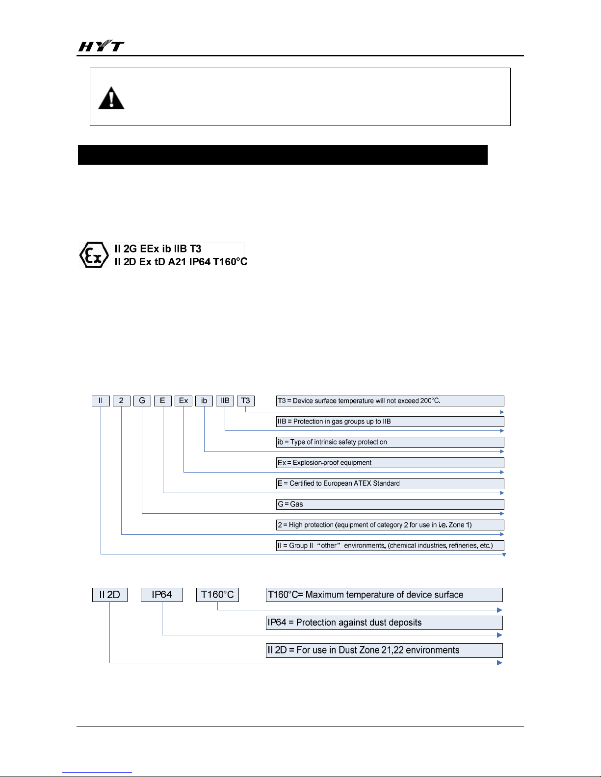
ATEX-Approved Intrinsically Safe Radio Information
ATEX-Approved Intrinsically Safe Radio
Certification
ATEX-approved Intrinsically Safe
ZELM 06 ATEX 0321
ATEX (Atmospheres Explosibles) Directive 94/9/EC
Introduced in 2003, this is the European Union directive to which all two-way radios must conformif used
in potentially explosive environments. It replaces the Cenelec classification in all European Union
member states and EFTA countries. All HYT professional series ATEX portable radios are approved to
ATEX Protection Classes II 2 G EEx ib IIB T3 and II 2D IP64 T160°C as interpreted in the following
tables:
ATEX Gas Protection:
ATEX Dust Protection:
Page 5
TC-700 Ex PLUS Service Manual
4
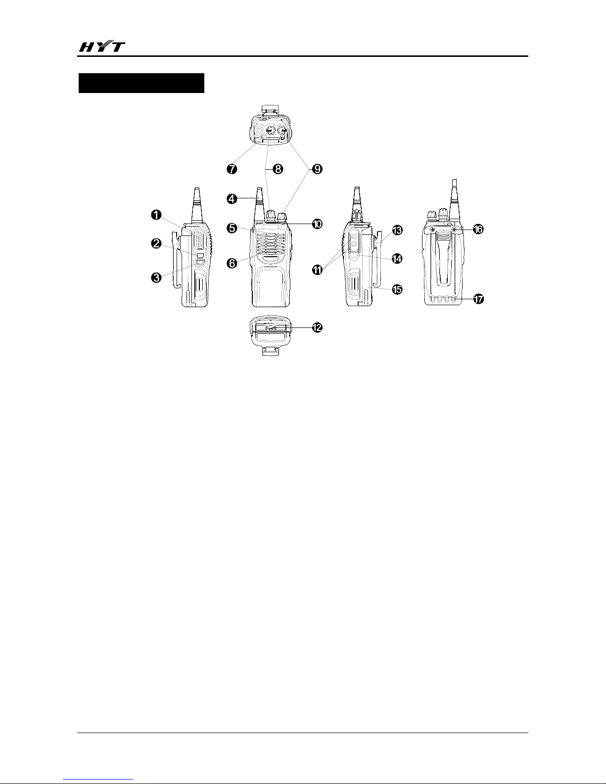
Radio Overview
1. PTT (Push-to-Talk) Key
Press and hold down the PTT key to transmit, release it to receive.
2. SK1 (Side Key 1) (programmable)
3. SK2 (Side Key 2) (programmable)
4. Antenna
5. Microphone
6. Speaker
7. TK (Top Key) (programmable)
8. Channel Selector Knob
Rotate the knob to select from channel 1 to 16.
9. Radio On-Off/Volume Control Knob
Rotate the knob clockwise to turn the radio on, rotate the knob fully counter-clockwise until a “click”
is heard to turn the radio off.
Turn the knob clockwise to increase the volume, or counter-clockwise to decrease the volume.
10. LED Indicator Table below explains the functions of the LEDs and beeps.
11. Accessory Jack
12. Battery Latch
13. Belt Clip
14. Accessory cover
15. Battery
16. Screw
17. Electrode Piece
Page 6
TC-700 Ex PLUS Service Manual
5
Wired Cloning Source radio: Turn the source radio on while
holding down the PTT and SK2.
Slave radio: Rotate the On-Off/Volume Control
knob clockwise to turn the slave radio on.
The orange LED flashes twice.
Source radio (power on the slave radio and
connect the cloning cable, then press the PTT
of source radio to initiate cloning.)
1) LED solidly glows red when
cloning progress;
2) LED goes out when cloning is
finished;
3) LED flashes red when cloning
fails.
Slave radio 1) LED solidly glows green when
cloning progress;
2) LED goes out when cloning is
finished.
Wireless
cloning
Turn on both the source radio and slave radio
while holding down the PTT and SK1. Both
radios are required to be on the same channel
for cloning.
The orange LED flashes once.
Source radio (turn on both the source radio and
slave radio while holding down the PTT and
SK1, then press the PTT of source radio while
both radios are on the same channel to initiate
cloning.)
LED solidly glows red when
cloning progress.
Slave radio 1) LED solidly glows green when
cloning progress;
2) LED flashes green and radio
sounds beep tone, when
cloning is finished;
3) LED flashes red when cloning
fails.
Power On The green LED flashes once.
Low Battery Alert LED flashes red, and radio sounds
three beeps every 30 seconds.
Transmitting LED glows red
Receiving LED glows green when carrier
presents.
Scanning Green LED flashes once every 1
second.
Programming Reading: LED glows red;
Writing: LED glows green.
Encoding (DTMF/PTT ID/2-Tone
(5-Tone)/HDC1200/HDC2400TM)
1) LED glows red while
transmitting;
2) LED glows orange when
transmission ends.
Page 7

TC-700 Ex PLUS Service Manual
6
Decoding (2-Tone (5-Tone)/HDC1200/HDC2400TM) Orange LED flashes after the
signalling is successfully decoded.
Select Power Level 0.5W: One beep is heard;
1.5W: Two beeps are heard;
3W: Three beeps are heard.
Function Key Press One beep to enable, two beeps to
disable.
Software Specifications
Specifications
Conventional Mode
1. Mechanical Selector Knob (16 channels)
VHF: 136-174 MHz
UHF: 420-470 MHz
2. Channel Spacing: 25/20/12.5KHz (programmable)
3. Step: 2.5/5/6.25KHz
4. LED Indicator: Red/Green/Orange
5. 3 Programmable Function Keys
6. CTCSS/CDCSS Encode & Decode
7. DTMF Encode
8. 2-Tone (5-Tone) Encode & Decode
9. HDC2400TMEncode & Decode
10. HDC1200 Encode & Decode
11. Squelch Mode:
1) Carrier
2) CTCSS/CDCSS
3) Optional Signalling
4) CTCSS/CDCSS AND 2-Tone (5-Tone)/ HDC2400TM/HDC1200
5) CTCSS/CDCSS OR 2-Tone / HDC2400TM/HDC1200
12. Scan
13. Time-Out-Timer (TOT)
14. Rental
15. Battery Save
16. Emergency
17. PTT ID
18. Busy Channel Lockout (Tx Admit Criteria)
Description
1. User Mode
This mode is for normal operation.
2. All Reset Mode
Firstly ground the SELF point, and then turn the radio on while holding down TK key for 2 seconds. The
radio enters all reset mode with green LED flashing twice. Turn the channel selector knob to the selected
channel and press PTT, the radio data is all reset (All clone modes will be automatically activated when
Page 8
TC-700 Ex PLUS Service Manual
7
All Reset is completed). Frequency settings are shown as follows:
Selected Channel
Frequency Band(MHz)
F1 (MHz) F2 (MHz) F3 (MHz) F4 (MHz) F5 (MHz)
1 136 - 174 (V)
TX1:136
RX1:136.1
TX2:145.5
RX2:145.6
TX3:155
RX3:155.1
TX4:164.5
RX4:164.6
TX5:174
RX5:173.9
2 400 - 450 (U1)
TX1:400
RX1:400.1
TX2:412.5
RX2:412.6
TX3:425
RX3:425.1
TX4: 437.5
RX4:437.6
TX5:450
RX5:449.9
3 440 - 490 (U2)
TX1:440
RX1:440.1
TX2:452.5
RX2:452.6
TX3:465
RX3:465.1
TX4:477.5
RX4:477.6
TX5:490
RX5:489.9
4 420 - 470 (U3)
TX1:420
RX1:420.1
TX2:432.5
RX2:432.6
TX3:445
RX3:445.1
TX4:457.5
RX4:457.6
TX5:470
RX5:469.9
5 470 - 520 (U4)
TX1:470
RX1:470.1
TX2:482.5
RX2:482.6
TX3:495
RX3:495.1
TX4:507.5
RX4:507.6
TX5:520
RX5:519.9
6 300 - 350 (U6)
TX1:300
RX1:300.1
TX2:312.5
RX2:312.6
TX3:325
RX3:325.1
TX4:337.5
RX4:337.6
TX5:350
RX5:349.9
7 350 - 390 (U5)
TX1:350
RX1:350.1
TX2:360
RX2:360.1
TX3:370
RX3:370.1
TX4:380
RX4:380.1
TX5:390
RX5:389.9
8 450 - 520 (U8)
TX1:450
RX1:450.1
TX2:467.5
RX2:467.6
TX3:485
RX3:485.1
TX4:502.5
RX4:502.6
TX5:520
RX5:519.9
9 400 - 470 (U7)
TX1:400
RX1:400.1
TX2:417.5
RX2:417.6
TX3:435
RX3:435.1
TX4:452.5
RX4:452.6
TX5:470
RX5:469.9
Channel data is shown as follows:
Channel Rx Frequency (MHZ) Tx Frequency (MHZ) Signalling Power Channel Spacing
1 RX1 TX1 None H 25KHZ
2 RX3 TX3 None H 25KHZ
3 RX5 TX5 None H 25KHZ
4 RX1 RX1 None LO 20KHZ
5 RX3 RX3 None LO 20KHZ
6 RX5 RX5 None LO 20KHZ
7 RX1 RX1 None LO 12.5KHZ
8 RX3 RX3 None LO 12.5KHZ
9 RX5 RX5 None LO 12.5KHZ
10 RX3 RX3 67HZ LO 25KHZ
11 RX3 RX3 254.1HZ LO 25KHZ
12 RX3 RX3 023 LO 25KHZ
13 RX3 RX3 754 LO 25KHZ
14 RX3 RX3 2-TONE LO 25KHZ
15 RX3 RX3 5-TONE LO 25KHZ
16 RX3 RX3 None LO 25KHZ
Page 9

TC-700 Ex PLUS Service Manual
8
3. Wireless Cloning Mode
Select wireless cloning from optional functions in programming software, turn the radio on while holding
down PTT and SK1 key simultaneously for 2 seconds, then the source and slave radios enter wireless
cloning mode with orange LED flashing once (when both radios are turned on and stay in the same
channel), hold down PTT on the source radio to begin cloning. During cloning progress, the source radio
emits red LED and the slave radio emits green LED. When cloning is finished, the slave radio flashes
green LED and emits Beep tone, and the source radio shuts off LED. If cloning failed, the slave radio
flashes red.
4. Wired Cloning Mode
Select Wired Cloning from optional functions in programming software, turn the radio on while holding
down PTT and SK2 key simultaneously for 2 seconds, then the source radio enters Wired Cloning mode
with orange LED flashing twice. Then simply turn the slave radio on. Hold down PTT on the source radio
to begin cloning. During cloning progress, the source radio emits red LED and the slave radio emits
green LED. When cloning is finished, both radios shut off LED. If cloning failed, the source radio flashes
red.
5. Manual Adjust Mode
Manual adjustment is performed to adjust frequency deviation, power, sensitivity, squelch, etc.
Note: Prior to entering this mode, select the Manual Adjust Mode from optional functions in
programming software.
The manual adjustment operations are detailed as follows:
(1) Enter the manual adjust mode
Turn the radio on by holding down TK and SK2 key simultaneously for 2 seconds, then the radio
enters manual adjust mode with red LED flashing twice.
(2) Channel number on the channel selector knob
Adjust the settings on the selected channel. Each changing of channel selects 25KHz channel
spacing and low frequency F1.
(3) SK2 key
Sets the frequency. 1 point tuning adjusts center frequency; 3 point tuning adjusts F1, F3, F5; 5
point tuning adjusts F1-F5.
The frequency toggles at a low to high cycle. Green LED flashes once when adjusting F1.
(4) TK key
Use to toggle the channel spacing among 25 KHz, 20 KHz and 12.5 KHz. Red LED flashes once
when the 25 KHz is selected.
(5) PTT/SK1
PTT→ Increase
SK1→ Decrease
PTT/SK1 is pressed to increase or decrease the value of the adjusting item. Red LED glows
indicating the maximum value and green LED indicating the minimum value. Hold down the key to
increase or decrease the value continuously.
Press PTT key to save the BATT LOW, VOX and SQL settings, then green LED glows once.
(6) Select adjustment group
The first group of adjustment items is selected once the radio enters the manual adjust mode.
Select the 16thchannel and press PTT key to enter the next group. Press it again to return to the first
group. Orange LED flashes once when the first group is selected and flashes twice when the
second group is selected.
Page 10
TC-700 Ex PLUS Service Manual
9
(7) Frequency Setting
5 point tuning (MHz) TX: { TX1,TX2,TX3,TX4,TX5}
RX: { RX1,RX2,RX3,RX4,RX5}
3 point tuning (MHz) TX: { TX1, TX3, TX5}
RX: { RX1, RX3, RX5}
1 point tuning (MHz) TX: { TX3}
RX: { RX3}
6. PC Tuning Mode
Select tuning mode of programming items in the programming software and then tuning as the setting.
First Group of Adjustment Items
Channel No. Adjustment Item Remarks
25KHz 20KHz 12.5KHz
1 Tx power LOW 5 point tuning
2 CDCSS PLL balance 3 point tuning (wide)
3 CDCSS deviation 3 point tuning (wide) 1 point tuning 1 point tuning (narrow)
4 CTCSS deviation LOW (67Hz) 3 point tuning (wide) 1 point tuning 1 point tuning (narrow)
5
CTCSS deviation CENTER
(136.5Hz)
3 point tuning (wide) 1 point tuning
1 point tuning (narrow)
6 CTCSS deviation HIGH (254.1Hz) 3 point tuning (wide) 1 point tuning 1 point tuning (narrow)
7 AK2346 audio deviation (TX) 3 point tuning (wide) 1 point tuning 3 point tuning (narrow)
8 2 TONE deviation 1 point tuning (wide) 1 point tuning 1 point tuning (narrow)
9 DTMF deviation 1 point tuning (wide) 1 point tuning 1 point tuning (narrow)
10 MSK deviation 3 point tuning (wide) 1 point tuning 1 point tuning (narrow)
11 TX power HIGH 5 point tuning
12 TX voltage LOW 1 point tuning
Second Group of Adjustment Items
Channel No.
AdjustmentItem
Remarks
25KHz 20KHz 12.5KHz
1 RX sensitivity 5 point tuning
2 AK2346 volume (RX) 1 point tuning (wide) 1 point tuning 1 point tuning (narrow)
3 Squelch level 3 (OPEN) 5 point tuning (wide) 1 point tuning 3 point tuning (narrow)
4 Squelch level 3 (SQUELCH) 5 point tuning (wide) 1 point tuning
3 point tuning (narrow)
5 Squelch level 9 (OPEN) 5 point tuning (wide) 1 point tuning
3 point tuning (narrow)
6 Squelch level 9 (SQUELCH) 5 point tuning (wide) 1 point tuning 3 point tuning (narrow)
7 RX voltage LOW 1 point tuning
Page 11
TC-700 Ex PLUS Service Manual
10
Circuit Description
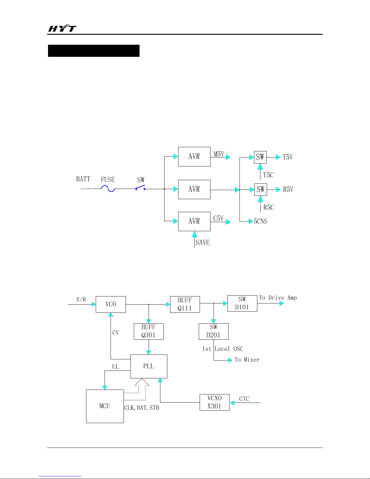
Power Supply
The radio power is supplied by the battery. The power supply is from B+, and supplies power SWB+ for
the three AVRs, after passing through fuse FE250mA and switch. IC504 supplies 5V (M5V) voltage for
the control circuit. And IC503 supplies 5V (C5V) voltage for the shared circuit. IC502 supplies voltage for
the transmit/receive circuit. While transmitting, T5C becomes low level and Q502 is turned on to supply
5V (T5V) voltage for the transmit circuit. While receiving, R5C becomes low level and Q504 is turned on
to supply 5V (R5V) voltage for the receive circuit. Power supply for RF is from B+ and works after
passing through fuse FE4 2A. Power supply for audio PA is from B+ and works after passing through
fuse FE5 0.5A.
Fig. 1 Power Supply Block Diagram
PLL Frequency Synthesizer
PLL circuit generates the first local oscillator signal for receive and RF signal for transmit.
Fig.2 PLL Block Diagram
Page 12
TC-700 Ex PLUS Service Manual
11
1. PLL Circuit
Step frequency of PLL can be 2.5 KHz, 5.0 KHz or 6.25 KHz. A 16.8MHz reference oscillator signal is
divided at IC301 by a counter to generate a 2.5 KHz, 5.0 KHz or 6.25 KHz reference frequency. Output
signal from VCO is buffer amplified by Q301 and divided at IC301 by a frequency divider. The divided
signal is compared with 2.5 KHz, 5.0 KHz or 6.25 KHz reference signal in the phase comparator of IC301.
The output signal from phase comparator is filtered through a low pass filter to generate a level D.C., and
the level D.C. controls oscillator frequency by controlling VCO.
2. VCO
The operating frequency is generated by Q302 in transmit mode and by Q307 in receive mode.
Operating frequency generate a control voltage by phase comparator to control varactor so that the
oscillator frequency is consistent with the MCU preset frequency (D301、D302、D303 and D304 in
transmit mode, and D307、D308、D309 and D310 in receive mode). T/R pin is set high level in receive
mode, and low level in transmit mode. The output from Q302 and Q307 is amplified by Q304 and sent to
buffer amplifier.
3. Unlock Detector
An unlock condition appears if low level occurs at MUXOUT pin of IC301. Transmission is inhibited if this
condition is detected by microprocessor.
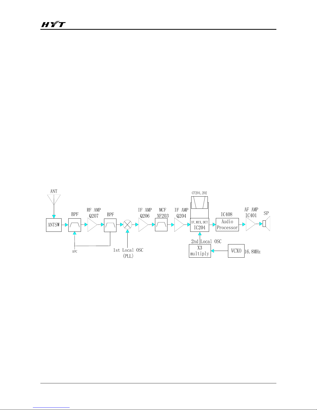
Receiver
The receiver utilizes double conversion superheterodyne (UHF)/(VHF).
Fig. 3 Receiver Section Configuration
1. Front-end RF Amplifier
The signal from antenna is amplified at RF amplifier (Q207) after passing through a
transmit/receive circuit and a band pass filter. Before passing the first mixer, the amplified
signal is filtered through another band pass filter to remove unwanted signals.
2. First Mixer
The signal from RF amplifier is mixed with the first local from PLL frequency synthesizer circuit at the fix
mixer (IC202) to create a 49.95MHz first IF signal. The first IF signal is then fed through a crystal filter
(XF203) to further remove unwanted signals.
3. IF Amplifier
The first IF signal is amplified by Q206 before passing through crystal filter and by Q204 after crystal
filter and then enters IF processing chip IC204. The signal from IC204 is mixed with the second oscillator
signal again in IC204 to create a 450 KHz second IF signal. The second IF signal then passes through a
Page 13
TC-700 Ex PLUS Service Manual
12
450KHz ceramic filter (wide: CF201,narrow: CF202) to eliminate unwanted signals before it is amplified
and detected in IC204.
4. Narrow/Wide Switch Circuit
Pin WCON and pin NCON of IC500 outputs wide (high level) and narrow (low level) channel spacing
signal respectively to turn on corresponding diode-connector, and to choose ceramic filter CF201 (wide)
or CF202 (narrow) to filter useless spurious signal.
5. AF Amplifier
The resulting AF signal from IC204 enters baseband processing chip IC408. The processed AF signal is
then amplified by an AF power amplifier (IC401) to drive the speaker.
Transmitter
1. AF and Signalling
AF signal from the microphone is amplified and low-pass-filtered in IC402 before it enters baseband
processing chip IC408, which also enters CTCSS/CDCSS/DTMF/2-Tone (5-Tone) signalling generated
by CPU. The IC408 processed mixing signal enters VCO for direct FM modulation (see fig.5).
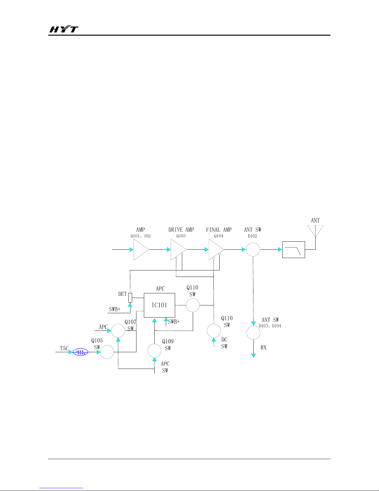
2. RF Power Amplifier
The transmit signal from VCO buffer amplifier (Q111) is amplified by Q101 and Q102. The amplified
signal is then amplified by the power amplifier Q103 and Q104 (including a two-stage FET amplifier) to
create 4.0W (UHF)/5.0W (VHF) RF power (see Fig. 6).
Fig. 4 APC System
3. Antenna Switch and LPF
Output signal from RF amplifier passes through a low-pass filter network and a transmit/receive switch
circuit comprised of D102, D103 and D104 before it reaches the antenna terminal. D103 and D104 is
turned on (conductive) in transmit mode and off (isolated) in receive mode.
Page 14
TC-700 Ex PLUS Service Manual
13
4. APC
The automatic power control (APC) circuit stabilizes the transmit power by detecting the drain current of
final stage amplifier FET. IC101 (2/2) compares the preset reference voltage with the voltage obtained
from final current. APC voltage is in proportion to the difference between auto detect voltage and
reference voltage output from IC101 (1/2). The output voltage controls FET power.
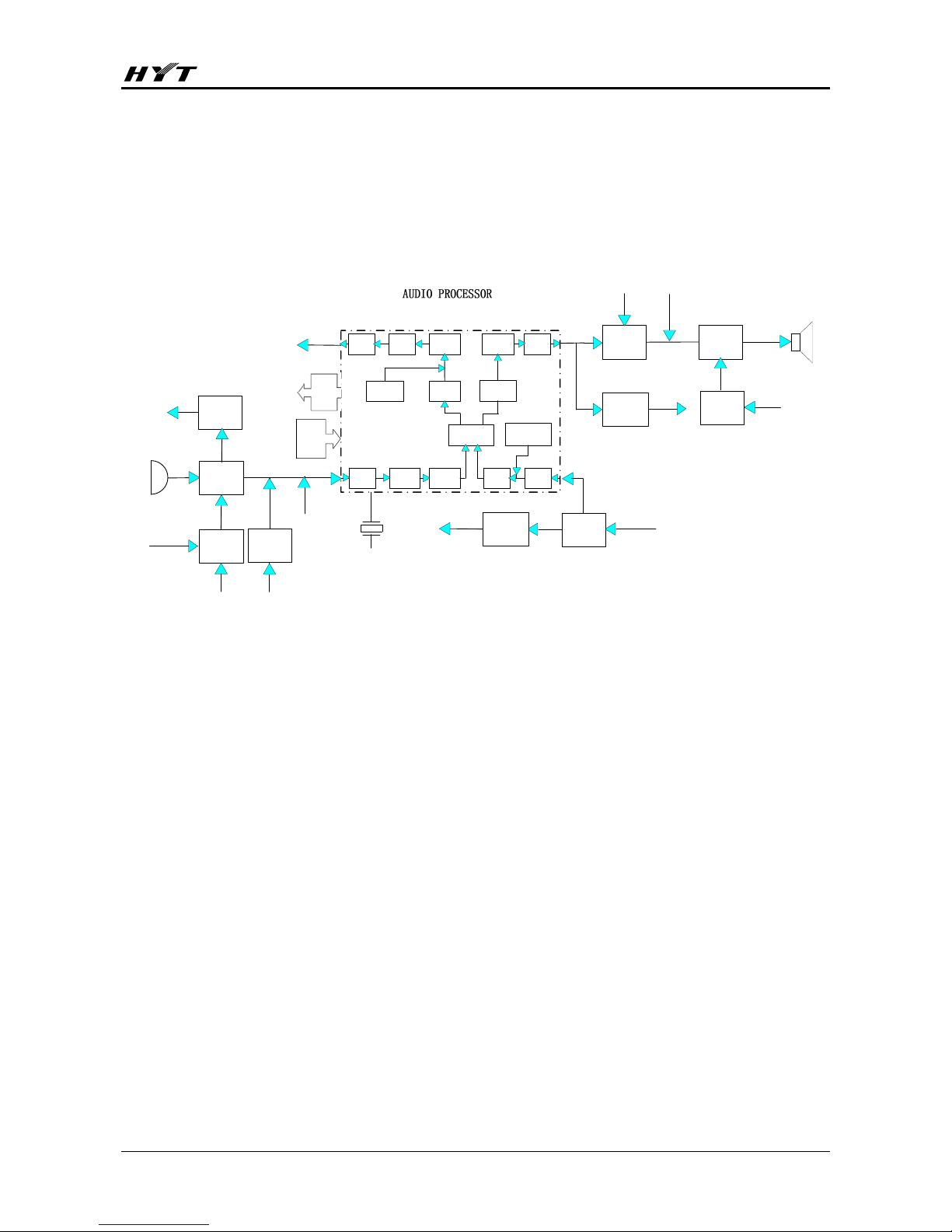
Baseband and Signalling System
The block diagram of signalling section is shown as figure 5.
AF DET
IC404
AMP LPF
IC405
LPF
CTCSS/CDCSS
TI
RXIN/RXINO
IC401
AMP
SP
AFCO
AFMUTE
MIC
Q401
SW
IC402
AMP LPF
D402
RB706F-40
VOX
MIC MUTE
5CNS
PTT
TONEO
Q406
Q407
SW
Q403
SW
Q404
SW
ALM/BP
IC408
AK2346
VR1
Scrambler
DeScrambler
VR3RXLPF
PreEmphasis
COMpressor
SMF VR4ExpandSplatterVR2
Limiter
De-
Emphasis
MSK
Modulator
MSK
Demodulator
MOD
IC407
BPF
TONEI
AFCK
CODIO
AFRDF
AFDT
AFSK
AFDIR
1/2OSD
TONEO
Fig. 5 AF and Signalling Circuit
1. CTCSS/CDCSS
Transmit: CTCSS/CDCSS signalling produced by CTCSS-PLL pass a low pass filter and then enters
VCXO. CTCSS/CDCSS signalling produced by CTCSS-OUT pass a low pass filter and then mixed with
AF before enters VCO.
Receive: Demodulated signal enters MCU after pass IC404、 IC405. MCU then judges whether
CTCSS/CDCSS matches the preset values or not.According the result, the out tone will be controlled by
AFMUTE.
2. 2-Tone (5-Tone) and DTMF
Transmit: The signal produced by MCU provides a Tx and SP output tone, and is then applied to the
baseband processing IC. The signal in mixed with the audio signal and goes to the VCO.
Receive: Demodulated signal is filtered after passing baseband processing IC, and then enters MCU for
decoding.
3. MSK
Transmit: MSK signal produced by baseband processing IC enters VCO together with AF signal for
modulation.
Receive: MSK input of demodulating IC is sent to AK2346 for demodulation after being amplified. The
demodulated signal is then sent to MCU for decoding.
4. AF
Transmit: AF signal from MIC enters baseband processed IC for amplification, pre-emphasis etc. after
being amplified. And then it enters VCO for modulation.
Receive: Demodulated AF signal enters the baseband processing IC for amplification, de-emphasis,
Page 15

TC-700 Ex PLUS Service Manual
14
etc., after being amplified.And then it enters AF PA driven speaker.
Baseband processed chip provides functions for processing signal as amplifying, filtering, emphasizing,
scrambling, companding, and amplitude limiting.
Control System
The IC500 CPU operates at 9.8304 MHz.
The block diagram of MCU control system is shown as the following figure:
Fig.6 MCU Block Diagram
Circuit in this section is mainly comprised of MCU, EEPROM etc.
MCU control circuit accomplishes the following functions: accomplish the reset initialization according to
the programmed feature of the radio when power on; detect keying signal and monitor battery voltage;
send necessary frequency data to PLL according to encode of the channel; switch and control
transmit/receive according to the signal input from PTT; turn on/off the mute circuit according to the input
signalling decode signal and squelch level signal; output control signal to control the light/off of LED;
control signalling process IC to perform tasks.
EEPROM
CTCSS/CDCSS
Code
Page 16
TC-700 Ex PLUS Service Manual
15
CPU Pins
No. MCU Port Port Name Input/Output Features
1 P94/DA1 APC/TV O Automatic Power Control
2 P93/DA0 TONEO O DTMF/2-Tone (5-Tone)/Beep tone output/ ALARM tone output
3 P92/TB2IN NC O NC
4 P91 O
5 P90 SHIFT O Clock beat-frequency
6 BYTE BYTE I
7 CNVSS CNVSS I
8 P87/XCIN O
9 P86/XCOUT O
10 RESET RESET I Input low level to enter all reset mode
11 XOUT XOUT O Crystal oscillator output pin
12 VSS GND I GND
13 XIN XIN I Crystal oscillator output pin
14 VCC VCC I VCC
15 P85/NMI NMI I
16 P84/INT2 AFCK I 2346 TCLK
17 P83/INT1 AUX1 O Indication for external scrambler
18 P82/INT0 AFRDF I
2346 RDF
19 P81 O
20 P80 PTTCO O PTTCO
21 P77 NC O
22 P76/TA3O CTCOUT O CTC _OUT (PWM) TO VCO
23 P75 NC O
24 P74/TA2O CTC_PLL O CTC_PLL (PWM)
25 P73 COM5 O Indication for receive/transmit status
26 P72/TA1O 1/2OSC O
27 P71/RxD2/TB5IN TONEI O
28 P70/TxD2
29 P67/TxD1 TXD O Serial date output.
30 P66/RxD1 RXD I Serial date input.
31 P65 I
32 P64 O
33 P63/TxD0 I COM4
34 P62/RxD0 O COM3
35 P61 COM1
Page 17
TC-700 Ex PLUS Service Manual
16
No. MCU Port Port Name Input/Output Features
36 P60 COM2
37 P57/RDY EEDAT I/O EEPROM DATA, date input/output.
38 P56/ALE EECLK O EEPROM CLK
39 P55/HOLD I
40 P54/HLDA AFDIR O AK2346 DIR
41 P53/BLCK AFSCK O 2346 SCLK
42 P52/RD NC O
43 P51/BHE AFDT O 2346 TDATA
44 P50/WR WE I
45 P47/CS3 CODIO I/O Common date control (AK2346 DATA).
46 P46/CS2
47 P45/CS1 SAVE O SAVE, power save control
48 P44/CS0 R5C O R5C Rx circuit power supply control
49 P43/A19 T5C O T5C Tx circuit power supply control
50 P42/A18
51 P41/A17
52 P40/A16
53 P37/A15
54 P36/A14
55 P35/A13
56 P34/A12
57 P33/A11
58 P32/A10
59 P31/A9
60 Vcc VCC I VCC
61 P30/A8 NCON O Narrow control
62 Vss GND I GND
63 P27/A7 AFCO O AFCO
64 P26/A6 WCON O Wide control
65 P25/A5 LEDR O Red LED control: H, lit; L, goes out
66 P24/A4 LEDG O Green LED control: H, lit; L, goes out
67 P23/A3 EN2 I EN2
68 P22/A2 EN4 I EN4
69 P21/A1 EN3 I EN3
70 P20/A0 EN1 I EN1
71 P17/INT5
72 P16/INT4 AFMUTE
Page 18
TC-700 Ex PLUS Service Manual
17
No. MCU Port Port Name Input/Output Features
73 P15/INT3
74 P14 TK I ALARM
75 P13 DC-Switch O
76 P12 PLL_UL I PLL unlock detect
77 P11 PLL_STB O PLL strobe output
78 P10 MICMUTE O MICMUTE
79 P07/D7 Option1 I
80 P06/D6 PLL_DATA O PLL date input
81 P05/D5 PLL_CLK O PLL clock output
82 P04/D4 T/R O Receive/transmit control
83 P03/D3 APC-Switch O
84 P02/D2 PTT I PTT
85 P01/D1 SK1 I MONI
86 P00/D0 SK2 I FK
87 P107/AN7 I MIC signal input
88 P106/AN6 BATT I BATT, battery voltage detect
89 P105/AN5 BATTSEL I Battery detect
90 P104/AN4 NC I
91 P103/AN3 SELF I Reset mode control: ground this pin to enter reset mode.
92 P102/AN2 RSSI I RSSI detect pin
93 P101/AN1 SQL I Squelch level input
94 AVSS GND I
95 P100/AN0 CTCIN I CTCSS input
96 VREF VCC I A/D conversion reference voltage
97 AVCC VCC I A/D conversion po
98 P97 O
99 P96 O
100 P95 O
Page 19
TC-700 Ex PLUS Service Manual
18
Parts List 1
TC-700 Ex PLUS VHF Parts List 1
No. Material No. Description Qty. Ref No. Print No.
1 3001050000000 Chip resistor 0402 0Ω J 1/16W 1 R147 T5F
2 3001050000000 Chip resistor 0402 0Ω J 1/16W 1 R254 T1G
3 3001050000000 Chip resistor 0402 0Ω J 1/16W 1 R303 B3G
4 3001050000000 Chip resistor 0402 0Ω J 1/16W 1 R315 B4I
5 3001050000000 Chip resistor 0402 0Ω J 1/16W 1 R318 B4I
6 3001050000000 Chip resistor 0402 0Ω J 1/16W 1 R319 B4I
7 3001050000000 Chip resistor 0402 0Ω J 1/16W 1 R402 T1F
8 3001050000000 Chip resistor 0402 0Ω J 1/16W 1 R404 B3K
9 3001050000000 Chip resistor 0402 0Ω J 1/16W 1 R406 B2J
10 3001050000000 Chip resistor 0402 0Ω J 1/16W 1 R424 R444
11 3001050000000 Chip resistor 0402 0Ω J 1/16W 1 R444 B2I
12 3001050000000 Chip resistor 0402 0Ω J 1/16W 1 R453 B3K
13 3001050000000 Chip resistor 0402 0Ω J 1/16W 1 R457 B3K
14 3001050000000 Chip resistor 0402 0Ω J 1/16W 1 R495 B3J
15 3001050000000 Chip resistor 0402 0Ω J 1/16W 1 R497 T1H
16 3001050000000 Chip resistor 0402 0Ω J 1/16W 1 R504 T5I
17 3001050000000 Chip resistor 0402 0Ω J 1/16W 1 R510 T3K
18 3001050000000 Chip resistor 0402 0Ω J 1/16W 1 R519 T1I
19 3001050000000 Chip resistor 0402 0Ω J 1/16W 1 R590 B3K
20 3001050000000 Chip resistor 0402 0Ω J 1/16W 1 R608 T1G
21 3001050000000 Chip resistor 0402 0Ω J 1/16W 1 R609 T1G
22 3001051000000 Chip resistor 0402 10Ω J 1/16 1 R152 B3G
23 3001051000000 Chip resistor 0402 10Ω J 1/16 1 R214 B2G
24 3001051000000 Chip resistor 0402 10Ω J 1/16 1 R344 B2I
25 3001051000000 Chip resistor 0402 10Ω J 1/16 1 R348 B4J
26 3001051000000 Chip resistor 0402 10Ω J 1/16 1 R349 B5I
27 3001051000000 Chip resistor 0402 10Ω J 1/16 1 R350 B5I
28 3001051000000 Chip resistor 0402 10Ω J 1/16 1 R456 T2E
29 3001051010000 Chip resistor 0402 100Ω J 1/1 1 R222 B1G
30 3001051010000 Chip resistor 0402 100Ω J 1/1 1 R223 B1E
31 3001051010000 Chip resistor 0402 100Ω J 1/1 1 R301 B3I
32 3001051010000 Chip resistor 0402 100Ω J 1/1 1 R305 B4G
33 3001051010000 Chip resistor 0402 100Ω J 1/1 1 R308 B4G
34 3001051010000 Chip resistor 0402 100Ω J 1/1 1 R335 B3I
35 3001051010000 Chip resistor 0402 100Ω J 1/1 1 R346 B2I
36 3001051010000 Chip resistor 0402 100Ω J 1/1 1 R454 T1D
37 3001051010000 Chip resistor 0402 100Ω J 1/1 1 R605 T2A
38 3001051020010 Chip resistor 0402 1KΩ J 1/16 1 R228 B1E
39 3001051020010 Chip resistor 0402 1KΩ J 1/16 1 R311 B4G
40 3001051020010 Chip resistor 0402 1KΩ J 1/16 1 R317 B4I
41 3001051020010 Chip resistor 0402 1KΩ J 1/16 1 R352 B5I
42 3001051020010 Chip resistor 0402 1KΩ J 1/16 1 R405 B3K
43 3001051020010 Chip resistor 0402 1KΩ J 1/16 1 R466 T1J
44 3001051020010 Chip resistor 0402 1KΩ J 1/16 1 R468 T1C
45 3001051020010 Chip resistor 0402 1KΩ J 1/16 1 R512 T4I
46 3001051020010 Chip resistor 0402 1KΩ J 1/16 1 R522 T2H
47 3001051020010 Chip resistor 0402 1KΩ J 1/16 1 R534 T3I
48 3001051020010 Chip resistor 0402 1KΩ J 1/16 1 R550 T2J
Page 20

TC-700 Ex PLUS Service Manual
19
No. Material No. Description Qty. Ref No. Print No.
49 3001051020010 Chip resistor 0402 1KΩ J 1/16 1 R551 T4J
50 3001051020010 Chip resistor 0402 1KΩ J 1/16 1 R553 T2I
51 3001051020010 Chip resistor 0402 1KΩ J 1/16 1 R555 T4J
52 3001051020010 Chip resistor 0402 1KΩ J 1/16 1 R560 T2I
53 3001051020010 Chip resistor 0402 1KΩ J 1/16 1 R563 T4I
54 3001051020010 Chip resistor 0402 1KΩ J 1/16 1 R565 T3K
55 3001051020010 Chip resistor 0402 1KΩ J 1/16 1 R566 T3K
56 3001051030000 Chip resistor 0402 10KΩ J 1/1 1 R112 B4E
57 3001051030000 Chip resistor 0402 10KΩ J 1/1 1 R141 T4E
58 3001051030000 Chip resistor 0402 10KΩ J 1/1 1 R201 B2F
59 3001051030000 Chip resistor 0402 10KΩ J 1/1 1 R321 B4J
60 3001051030000 Chip resistor 0402 10KΩ J 1/1 1 R336 B5J
61 3001051030000 Chip resistor 0402 10KΩ J 1/1 1 R347 B4I
62 3001051030000 Chip resistor 0402 10KΩ J 1/1 1 R407 B3K
63 3001051030000 Chip resistor 0402 10KΩ J 1/1 1 R418 T3F
64 3001051030000 Chip resistor 0402 10KΩ J 1/1 1 R426 B3K
65 3001051030000 Chip resistor 0402 10KΩ J 1/1 1 R432 T1J
66 3001051030000 Chip resistor 0402 10KΩ J 1/1 1 R440 T1E
67 3001051030000 Chip resistor 0402 10KΩ J 1/1 1 R442 B3K
68 3001051030000 Chip resistor 0402 10KΩ J 1/1 1 R461 T1K
69 3001051030000 Chip resistor 0402 10KΩ J 1/1 1 R463 T1J
70 3001051030000 Chip resistor 0402 10KΩ J 1/1 1 R467 T1J
71 3001051030000 Chip resistor 0402 10KΩ J 1/1 1 R471 B2K
72 3001051030000 Chip resistor 0402 10KΩ J 1/1 1 R476 B2K
73 3001051030000 Chip resistor 0402 10KΩ J 1/1 1 R480 B3K
74 3001051030000 Chip resistor 0402 10KΩ J 1/1 1 R482 B3J
75 3001051030000 Chip resistor 0402 10KΩ J 1/1 1 R485 B3J
76 3001051030000 Chip resistor 0402 10KΩ J 1/1 1 R487 B4J
77 3001051030000 Chip resistor 0402 10KΩ J 1/1 1 R489 B4J
78 3001051030000 Chip resistor 0402 10KΩ J 1/1 1 R508 T2J
79 3001051030000 Chip resistor 0402 10KΩ J 1/1 1 R517 T4K
80 3001051030000 Chip resistor 0402 10KΩ J 1/1 1 R630 T2G
81 3001051030000 Chip resistor 0402 10KΩ J 1/1 1 R631 T3G
82 3001051030000 Chip resistor 0402 10KΩ J 1/1 1 R632 T3G
83 3001051040010 Chip resistor 0402 100KΩ J 1/ 1 R146 T4F
84 3001051040010 Chip resistor 0402 100KΩ J 1/ 1 R212 B2G
85 3001051040010 Chip resistor 0402 100KΩ J 1/ 1 R218 T1H
86 3001051040010 Chip resistor 0402 100KΩ J 1/ 1 R234 B3D
87 3001051040010 Chip resistor 0402 100KΩ J 1/ 1 R235 B3C
88 3001051040010 Chip resistor 0402 100KΩ J 1/ 1 R240 B3B
89 3001051040010 Chip resistor 0402 100KΩ J 1/ 1 R241 B3D
90 3001051040010 Chip resistor 0402 100KΩ J 1/ 1 R242 B3B
91 3001051040010 Chip resistor 0402 100KΩ J 1/ 1 R253 B3C
92 3001051040010 Chip resistor 0402 100KΩ J 1/ 1 R310 B4G
93 3001051040010 Chip resistor 0402 100KΩ J 1/ 1 R400 T1G
94 3001051040010 Chip resistor 0402 100KΩ J 1/ 1 R403 T1F
95 3001051040010 Chip resistor 0402 100KΩ J 1/ 1 R428 B2J
96 3001051040010 Chip resistor 0402 100KΩ J 1/ 1 R429 T1J
97 3001051040010 Chip resistor 0402 100KΩ J 1/ 1 R430 T1J
98 3001051040010 Chip resistor 0402 100KΩ J 1/ 1 R448 B4K
99 3001051040010 Chip resistor 0402 100KΩ J 1/ 1 R475 B2K
100 3001051040010 Chip resistor 0402 100KΩ J 1/ 1 R486 T1H
Page 21

TC-700 Ex PLUS Service Manual
20
No. Material No. Description Qty. Ref No. Print No.
101 3001051040010 Chip resistor 0402 100KΩ J 1/ 1 R493 B3J
102 3001051040010 Chip resistor 0402 100KΩ J 1/ 1 R516 T4K
103 3001051040010 Chip resistor 0402 100KΩ J 1/ 1 R557 T2I
104 3001051040010 Chip resistor 0402 100KΩ J 1/ 1 R559 T4K
105 3001051050020 Chip resistor 0402 1MΩ J 1/16 1 R142 T4E
106 3001051050020 Chip resistor 0402 1MΩ J 1/16 1 R462 T1K
107 3001051050020 Chip resistor 0402 1MΩ J 1/16 1 R474 B2J
108 3001051050020 Chip resistor 0402 1MΩ J 1/16 1 R634 T2G
109 3001051230000 Chip resistor 0402 12KΩ J 1/1 1 R238 B3B
110 3001051230000 Chip resistor 0402 12KΩ J 1/1 1 R483 B3J
111 3001051240000 Chip resistor 0402 120KΩ J 1/ 1 R339 B3I
112 3001051520000 Chip resistor 0402 1.5KΩ J 1/ 1 R203 B1G
113 3001051530000 Chip resistor 0402 15KΩ J 1/1 1 R409 B3J
114 3001051530000 Chip resistor 0402 15KΩ J 1/1 1 R469 T1H
115 3001051530000 Chip resistor 0402 15KΩ J 1/1 1 R498 B2J
116 3001051540000 Chip resistor 0402 150KΩ F 1/ 1 R138 T5F
117 3001051540000 Chip resistor 0402 150KΩ F 1/ 1 R139 T4F
118 3001051540000 Chip resistor 0402 150KΩ F 1/ 1 R425 T1E
119 3001051540000 Chip resistor 0402 150KΩ F 1/ 1 R464 T1K
120 3001051540000 Chip resistor 0402 150KΩ F 1/ 1 R465 T1K
121 3001051540020 Chip resistor 0402 150KΩ J 1/ 1 R307 B4G
122 3001051540020 Chip resistor 0402 150KΩ J 1/ 1 R351 B5I
123 3001051800000 Chip resistor 0402 18Ω J 1/16 1 R231 B2E
124 3001051820000 Chip resistor 0402 1.8KΩ J 1/ 1 R217 B1F
125 3001051820000 Chip resistor 0402 1.8KΩ J 1/ 1 R416 T2B
126 3001051830000 Chip resistor 0402 18KΩ J 1/1 1 R421 B1I
127 3001051830000 Chip resistor 0402 18KΩ J 1/1 1 R422 B1I
128 3001051830000 Chip resistor 0402 18KΩ J 1/1 1 R438 T1E
129 3001051830000 Chip resistor 0402 18KΩ J 1/1 1 R451 B4K
130 3001051830000 Chip resistor 0402 18KΩ J 1/1 1 R452 B4K
131 3001051840000 Chip resistor 0402 180KΩ J 1/ 1 R337 B3I
132 3001051840000 Chip resistor 0402 180KΩ J 1/ 1 R446 B4J
133 3001051840000 Chip resistor 0402 180KΩ J 1/ 1 R447 B4J
134 3001051840000 Chip resistor 0402 180KΩ J 1/ 1 R492 B3J
135 3001052200000 Chip resistor 0402 22Ω J 1/16 1 R104 B4F
136 3001052200000 Chip resistor 0402 22Ω J 1/16 1 R107 B4E
137 3001052200000 Chip resistor 0402 22Ω J 1/16 1 R309 B4G
138 3001052210000 Chip resistor 0402 220Ω J 1/1 1 R225 B1E
139 3001052220000 Chip resistor 0402 2.2KΩ J 1/ 1 R144 T4F
140 3001052220000 Chip resistor 0402 2.2KΩ J 1/ 1 R229 B1E
141 3001052220000 Chip resistor 0402 2.2KΩ J 1/ 1 R316 B4I
142 3001052220000 Chip resistor 0402 2.2KΩ J 1/ 1 R420 T3E
143 3001052230010 Chip resistor 0402 22KΩ J 1/1 1 R204 B1H
144 3001052230010 Chip resistor 0402 22KΩ J 1/1 1 R206 B1H
145 3001052230010 Chip resistor 0402 22KΩ J 1/1 1 R207 B1H
146 3001052230010 Chip resistor 0402 22KΩ J 1/1 1 R208 B1H
147 3001052230010 Chip resistor 0402 22KΩ J 1/1 1 R431 T1J
148 3001052230010 Chip resistor 0402 22KΩ J 1/1 1 R433 T1J
149 3001052230010 Chip resistor 0402 22KΩ J 1/1 1 R445 B4J
150 3001052230010 Chip resistor 0402 22KΩ J 1/1 1 R458 B3J
151 3001052230010 Chip resistor 0402 22KΩ J 1/1 1 R460 B3K
152 3001052230010 Chip resistor 0402 22KΩ J 1/1 1 R484 B3I
Page 22
TC-700 Ex PLUS Service Manual
21
No. Material No. Description Qty. Ref No. Print No.
153 3001052230010 Chip resistor 0402 22KΩ J 1/1 1 R494 B2J
154 3001052240000 Chip resistor 0402 220KΩ J 1/ 1 R302 B3I
155 3001052240000 Chip resistor 0402 220KΩ J 1/ 1 R345 B2I
156 3001052240000 Chip resistor 0402 220KΩ J 1/ 1 R439 B2I
157 3001052240000 Chip resistor 0402 220KΩ J 1/ 1 R477 B2K
158 3001052240000 Chip resistor 0402 220KΩ J 1/ 1 R548 B4A
159 3001052700000 Chip resistor 0402 27Ω J 1/16 1 R226 B1E
160 3001052710010 Chip resistor 0402 270Ω J 1/1 1 R150 B3G
161 3001052710010 Chip resistor 0402 270Ω J 1/1 1 R230 B1E
162 3001052710010 Chip resistor 0402 270Ω J 1/1 1 R232 B2E
163 3001052720000 Chip resistor 0402 2.7KΩ J 1/ 1 R211 B2G
164 3001052720000 Chip resistor 0402 2.7KΩ J 1/ 1 R219 B1G
165 3001052730000 Chip resistor 0402 27KΩ J 1/1 1 R401 T1E
166 3001052730000 Chip resistor 0402 27KΩ J 1/1 1 R499 T1E
167 3001052790000 Chip resistor 0402 2.7Ω J 1/1 1 R236 B2B
168 3001053310010 Chip resistor 0402 330Ω J 1/1 1 R103 B4F
169 3001053310010 Chip resistor 0402 330Ω J 1/1 1 R108 B4E
170 3001053320000 Chip resistor 0402 3.3KΩ J 1/ 1 R101 B3F
171 3001053320000 Chip resistor 0402 3.3KΩ J 1/ 1 R148 B3G
172 3001053320000 Chip resistor 0402 3.3KΩ J 1/ 1 R151 B3G
173 3001053320000 Chip resistor 0402 3.3KΩ J 1/ 1 R216 T1G
174 3001053330010 Chip resistor 0402 33KΩ J 1/1 1 R419 B2I
175 3001053330010 Chip resistor 0402 33KΩ J 1/1 1 R478 B2K
176 3001053340000 Chip resistor 0402 330KΩ J 1/ 1 R481 B3K
177 3001053910000 Chip resistor 0402 390Ω J 1/1 1 R123 B5E
178 3001053910000 Chip resistor 0402 390Ω J 1/1 1 R304 B4H
179 3001053910000 Chip resistor 0402 390Ω J 1/1 1 R314 B4G
180 3001053920010 Chip resistor 0402 3.9KΩ J 1/ 1 R106 B4F
181 3001053940000 Chip resistor 0402 390KΩ J 1/ 1 R449 B4K
182 3001053940000 Chip resistor 0402 390KΩ J 1/ 1 R523 T2H
183 3001054320000 Chip resistor 0402 4.3KΩ J 1/ 1 R237 B3C
184 3001054700000 Chip resistor 0402 47Ω J 1/16 1 R111 B4E
185 3001054710000 Chip resistor 0402 470Ω J 1/1 1 R415 T2B
186 3001054720000 Chip resistor 0402 4.7KΩ J 1/ 1 R118 B3G
187 3001054720000 Chip resistor 0402 4.7KΩ J 1/ 1 R205 B1H
188 3001054720000 Chip resistor 0402 4.7KΩ J 1/ 1 R209 B1H
189 3001054720000 Chip resistor 0402 4.7KΩ J 1/ 1 R213 B2G
190 3001054720000 Chip resistor 0402 4.7KΩ J 1/ 1 R312 B5G
191 3001054720000 Chip resistor 0402 4.7KΩ J 1/ 1 R313 B3G
192 3001054720000 Chip resistor 0402 4.7KΩ J 1/ 1 R320 B4I
193 3001054720000 Chip resistor 0402 4.7KΩ J 1/ 1 R459 T1J
194 3001054720000 Chip resistor 0402 4.7KΩ J 1/ 1 R490 B4K
195 3001054720000 Chip resistor 0402 4.7KΩ J 1/ 1 R496 T1H
196 3001054720000 Chip resistor 0402 4.7KΩ J 1/ 1 R520 T2G
197 3001054730000 Chip resistor 0402 47KΩ J 1/1 1 R102 B4F
198 3001054730000 Chip resistor 0402 47KΩ J 1/1 1 R113 B4E
199 3001054730000 Chip resistor 0402 47KΩ J 1/1 1 R145 T5F
200 3001054730000 Chip resistor 0402 47KΩ J 1/1 1 R215 T1H
201 3001054730000 Chip resistor 0402 47KΩ J 1/1 1 R414 T3E
202 3001054730000 Chip resistor 0402 47KΩ J 1/1 1 R443 B2I
203 3001054730000 Chip resistor 0402 47KΩ J 1/1 1 R488 B4J
204 3001054730000 Chip resistor 0402 47KΩ J 1/1 1 R502 T2K
Page 23

TC-700 Ex PLUS Service Manual
22
No. Material No. Description Qty. Ref No. Print No.
205 3001054730000 Chip resistor 0402 47KΩ J 1/1 1 R506 T5J
206 3001054730000 Chip resistor 0402 47KΩ J 1/1 1 R507 T2J
207 3001054730000 Chip resistor 0402 47KΩ J 1/1 1 R515 T1I
208 3001054730000 Chip resistor 0402 47KΩ J 1/1 1 R535 T5J
209 3001054730000 Chip resistor 0402 47KΩ J 1/1 1 R536 T5J
210 3001054730000 Chip resistor 0402 47KΩ J 1/1 1 R538 T5J
211 3001054730000 Chip resistor 0402 47KΩ J 1/1 1 R539 T4H
212 3001054730000 Chip resistor 0402 47KΩ J 1/1 1 R549 T2G
213 3001054730000 Chip resistor 0402 47KΩ J 1/1 1 R556 T2I
214 3001054730000 Chip resistor 0402 47KΩ J 1/1 1 R558 T3K
215 3001054730000 Chip resistor 0402 47KΩ J 1/1 1 R561 T3K
216 3001054740000 Chip resistor 0402 470KΩ J 1/ 1 R322 B3G
217 3001054740000 Chip resistor 0402 470KΩ J 1/ 1 R408 T1E
218 3001054790000 Chip resistor 0402 4.7Ω J 1/1 1 R411 T1E
219 3001054790000 Chip resistor 0402 4.7Ω J 1/1 1 R412 T2E
220 3001055110000 Chip resistor 0402 510Ω J 1/1 1 R251 B3C
221 3001055130010 Chip resistor 0402 51KΩ J 1/1 1 R479 B2K
222 3001055620000 Chip resistor 0402 5.6KΩ J 1/ 1 R117 B5E
223 3001055620000 Chip resistor 0402 5.6KΩ J 1/ 1 R149 B3G
224 3001055620000 Chip resistor 0402 5.6KΩ J 1/ 1 R410 T1E
225 3001055630000 Chip resistor 0402 56KΩ J 1/1 1 R472 B2K
226 3001055630000 Chip resistor 0402 56KΩ J 1/1 1 R473 B2K
227 3001056810000 Chip resistor 0402 680Ω J 1/1 1 R105 B4F
228 3001056820000 Chip resistor 0402 6.8KΩ J 1/ 1 R227 B1E
229 3001056820000 Chip resistor 0402 6.8KΩ J 1/ 1 R239 B2B
230 3001056820000 Chip resistor 0402 6.8KΩ J 1/ 1 R427 B3J
231 3001056830000 Chip resistor 0402 68KΩ J 1/1 1 R252 B2G
232 3001056830000 Chip resistor 0402 68KΩ J 1/1 1 R470 B2K
233 3001056840000 Chip resistor 0402 680KΩ J 1/ 1 R220 B1G
234 3001058220000 Chip resistor 0402 8.2KΩ J 1/ 1 R601 T1G
235 3001058230000 Chip resistor 0402 82KΩ J 1/1 1 R441 B2I
236 3001058230000 Chip resistor 0402 82KΩ J 1/1 1 R450 B4K
237 3001059130000 Chip resistor 0402 91KΩ F 1/1 1 R338 B3I
238 3001061800000 Chip resistor 0603 18Ω J 1/10 1 R109 B3F
239 3001064700000 Chip resistor 0603 47Ω J 1/10 1 R115 B5E
240 3001070000000 Chip resistor 0805 0Ω J 1/8W( 1 R114 B4E
241 3002996830000 Trimmer resistor(2*2) 68KΩ(+25%) 1 VR1 T2I
242 3003992220000 Thermistor 0603 2.2KΩ J 10 1 TH301 B3I
243 3003994730000 Thermistor 0603 47KΩ J 100 1 RTHE1 B5D
244 3005051020000 Resistor array 0402 1K*2 J 1/16 1 CP506 T4J
245 3005051020000 Resistor array 0402 1K*2 J 1/16 1 CP507 T3K
246 3005051020000 Resistor array 0402 1K*2 J 1/16 1 CP509 T2I
247 3005051020000 Resistor array 0402 1K*2 J 1/16 1 CP511 T2J
248 3005051020000 Resistor array 0402 1K*2 J 1/16 1 CP512 T2J
249 3005051020000 Resistor array 0402 1K*2 J 1/16 1 CP514 T4J
250 3005051020000 Resistor array 0402 1K*2 J 1/16 1 CP516 T4I
251 3005051020000 Resistor array 0402 1K*2 J 1/16 1 CP517 T4K
252 3005051020000 Resistor array 0402 1K*2 J 1/16 1 CP524 T4I
253 3005051020010 Resistor array 0402 1K*4 J 1/16 1 CP505 T2J
254 3005051020010 Resistor array 0402 1K*4 J 1/16 1 CP518 T3I
255 3005051020010 Resistor array 0402 1K*4 J 1/16 1 CP519 T3I
256 3005051020010 Resistor array 0402 1K*4 J 1/16 1 CP525 T4I
Page 24

TC-700 Ex PLUS Service Manual
23
No. Material No. Description Qty. Ref No. Print No.
257 3005051020010 Resistor array 0402 1K*4 J 1/16 1 CP526 T4J
258 3101050400010 Chip capacitor 0402 4PF B 50V 1 C202 B2F
259 3101050400010 Chip capacitor 0402 4PF B 50V 1 C233 B1F
260 3101050400010 Chip capacitor 0402 4PF B 50V 1 C268 B1E
261 3101051010030 Chip capacitor 0402 100PF J 50 1 C152 T4E
262 3101051010030 Chip capacitor 0402 100PF J 50 1 C248 B3D
263 3101051010030 Chip capacitor 0402 100PF J 50 1 C252 B3C
264 3101051010030 Chip capacitor 0402 100PF J 50 1 C264 B3B
265 3101051010030 Chip capacitor 0402 100PF J 50 1 C273 B3B
266 3101051010030 Chip capacitor 0402 100PF J 50 1 C329 B4I
267 3101051010030 Chip capacitor 0402 100PF J 50 1 C339 B5I
268 3101051010030 Chip capacitor 0402 100PF J 50 1 C340 B5J
269 3101051010030 Chip capacitor 0402 100PF J 50 1 C341 B5J
270 3101051010030 Chip capacitor 0402 100PF J 50 1 C605 T2C
271 3101051010030 Chip capacitor 0402 100PF J 50 1 C607 T2D
272 3101051020010 Chip capacitor 0402 1000PF K 5 1 C101 B3F
273 3101051020010 Chip capacitor 0402 1000PF K 5 1 C104 B4F
274 3101051020010 Chip capacitor 0402 1000PF K 5 1 C106 B4E
275 3101051020010 Chip capacitor 0402 1000PF K 5 1 C107 B4E
276 3101051020010 Chip capacitor 0402 1000PF K 5 1 C108 B4F
277 3101051020010 Chip capacitor 0402 1000PF K 5 1 C110 B4F
278 3101051020010 Chip capacitor 0402 1000PF K 5 1 C114 B4E
279 3101051020010 Chip capacitor 0402 1000PF K 5 1 C116 B4E
280 3101051020010 Chip capacitor 0402 1000PF K 5 1 C118 B5E
281 3101051020010 Chip capacitor 0402 1000PF K 5 1 C120 B4D
282 3101051020010 Chip capacitor 0402 1000PF K 5 1 C124 B3C
283 3101051020010 Chip capacitor 0402 1000PF K 5 1 C133 B4C
284 3101051020010 Chip capacitor 0402 1000PF K 5 1 C155 B3G
285 3101051020010 Chip capacitor 0402 1000PF K 5 1 C156 B3G
286 3101051020010 Chip capacitor 0402 1000PF K 5 1 C158 B3G
287 3101051020010 Chip capacitor 0402 1000PF K 5 1 C201 B2F
288 3101051020010 Chip capacitor 0402 1000PF K 5 1 C210 B2G
289 3101051020010 Chip capacitor 0402 1000PF K 5 1 C238 B1E
290 3101051020010 Chip capacitor 0402 1000PF K 5 1 C256 B2C
291 3101051020010 Chip capacitor 0402 1000PF K 5 1 C259 B3C
292 3101051020010 Chip capacitor 0402 1000PF K 5 1 C262 B3C
293 3101051020010 Chip capacitor 0402 1000PF K 5 1 C266 B3B
294 3101051020010 Chip capacitor 0402 1000PF K 5 1 C301 B4I
295 3101051020010 Chip capacitor 0402 1000PF K 5 1 C310 B4G
296 3101051020010 Chip capacitor 0402 1000PF K 5 1 C314 B4G
297 3101051020010 Chip capacitor 0402 1000PF K 5 1 C318 B5G
298 3101051020010 Chip capacitor 0402 1000PF K 5 1 C331 B4J
299 3101051020010 Chip capacitor 0402 1000PF K 5 1 C332 B4J
300 3101051020010 Chip capacitor 0402 1000PF K 5 1 C346 B3I
301 3101051020010 Chip capacitor 0402 1000PF K 5 1 C347 B2I
302 3101051020010 Chip capacitor 0402 1000PF K 5 1 C358 B4I
303 3101051020010 Chip capacitor 0402 1000PF K 5 1 C406 T1E
304 3101051020010 Chip capacitor 0402 1000PF K 5 1 C409 B2J
305 3101051020010 Chip capacitor 0402 1000PF K 5 1 C462 T1J
306 3101051020010 Chip capacitor 0402 1000PF K 5 1 C497 B5K
307 3101051020010 Chip capacitor 0402 1000PF K 5 1 C512 T2K
308 3101051020010 Chip capacitor 0402 1000PF K 5 1 C538 T5J
Page 25

TC-700 Ex PLUS Service Manual
24
No. Material No. Description Qty. Ref No. Print No.
309 3101051020010 Chip capacitor 0402 1000PF K 5 1 C546 T3K
310 3101051020010 Chip capacitor 0402 1000PF K 5 1 C558 B4A
311 3101051030020 Chip capacitor 0402 0.01UF K 2 1 C121 B4D
312 3101051030020 Chip capacitor 0402 0.01UF K 2 1 C147 B3D
313 3101051030020 Chip capacitor 0402 0.01UF K 2 1 C205 B2F
314 3101051030020 Chip capacitor 0402 0.01UF K 2 1 C219 B2G
315 3101051030020 Chip capacitor 0402 0.01UF K 2 1 C226 T1G
316 3101051030020 Chip capacitor 0402 0.01UF K 2 1 C230 B1G
317 3101051030020 Chip capacitor 0402 0.01UF K 2 1 C236 B1E
318 3101051030020 Chip capacitor 0402 0.01UF K 2 1 C237 B1E
319 3101051030020 Chip capacitor 0402 0.01UF K 2 1 C239 B1E
320 3101051030020 Chip capacitor 0402 0.01UF K 2 1 C241 B2E
321 3101051030020 Chip capacitor 0402 0.01UF K 2 1 C243 B2D
322 3101051030020 Chip capacitor 0402 0.01UF K 2 1 C250 B3D
323 3101051030020 Chip capacitor 0402 0.01UF K 2 1 C253 B2C
324 3101051030020 Chip capacitor 0402 0.01UF K 2 1 C304 B3H
325 3101051030020 Chip capacitor 0402 0.01UF K 2 1 C348 B2I
326 3101051030020 Chip capacitor 0402 0.01UF K 2 1 C357 B5G
327 3101051030020 Chip capacitor 0402 0.01UF K 2 1 C419 T2F
328 3101051030020 Chip capacitor 0402 0.01UF K 2 1 C450 B4K
329 3101051030020 Chip capacitor 0402 0.01UF K 2 1 C461 T1J
330 3101051030020 Chip capacitor 0402 0.01UF K 2 1 C465 T1K
331 3101051030020 Chip capacitor 0402 0.01UF K 2 1 C486 B4K
332 3101051030020 Chip capacitor 0402 0.01UF K 2 1 C539 T3A
333 3101051030020 Chip capacitor 0402 0.01UF K 2 1 C540 T3A
334 3101051030020 Chip capacitor 0402 0.01UF K 2 1 C541 T3A
335 3101051030020 Chip capacitor 0402 0.01UF K 2 1 C542 T3A
336 3101051030020 Chip capacitor 0402 0.01UF K 2 1 C545 T3I
337 3101051030020 Chip capacitor 0402 0.01UF K 2 1 C608 T1F
338 3101051030020 Chip capacitor 0402 0.01UF K 2 1 C636 T2G
339 3101051200020 Chip capacitor 0402 12PF J 50V 1 C247 B2D
340 3101051200020 Chip capacitor 0402 12PF J 50V 1 C249 B2D
341 3101051230000 Chip capacitor 0402 0.012UF K 1 C448 B4J
342 3101051500020 Chip capacitor 0402 15PF J 50V 1 C100 B3G
343 3101051500020 Chip capacitor 0402 15PF J 50V 1 C102 B3F
344 3101051500020 Chip capacitor 0402 15PF J 50V 1 C267 B3B
345 3101051500020 Chip capacitor 0402 15PF J 50V 1 C359 B4I
346 3101051500020 Chip capacitor 0402 15PF J 50V 1 C514 T4K
347 3101051510000 Chip capacitor 0402 150PF(±5%) 1 C105 B4F
348 3101051510000 Chip capacitor 0402 150PF(±5%) 1 C258 B3B
349 3101051510000 Chip capacitor 0402 150PF(±5%) 1 C473 B2K
350 3101051800010 Chip capacitor 0402 18PF J 50V 1 C103 B4F
351 3101051800010 Chip capacitor 0402 18PF J 50V 1 C203 B2F
352 3101051800010 Chip capacitor 0402 18PF J 50V 1 C204 B2F
353 3101051800010 Chip capacitor 0402 18PF J 50V 1 C207 B2F
354 3101051800010 Chip capacitor 0402 18PF J 50V 1 C245 B2D
355 3101051820000 Chip capacitor 0402 1800PF K 5 1 C222 T1G
356 3101051820000 Chip capacitor 0402 1800PF K 5 1 C430 B3J
357 3101051830000 Chip capacitor 0402 0.018UF K 1 C421 B2J
358 3101051830000 Chip capacitor 0402 0.018UF K 1 C492 B2J
359 3101052200010 Chip capacitor 0402 22PF J 50V 1 C360 B4I
360 3101052200010 Chip capacitor 0402 22PF J 50V 1 C361 B4I
Page 26

TC-700 Ex PLUS Service Manual
25
No. Material No. Description Qty. Ref No. Print No.
361 3101052200010 Chip capacitor 0402 22PF J 50V 1 C471 B1J
362 3101052200010 Chip capacitor 0402 22PF J 50V 1 C472 B1K
363 3101052210010 Chip capacitor 0402 220PF K 50 1 C211 B2G
364 3101052210010 Chip capacitor 0402 220PF K 50 1 C451 B4K
365 3101052210010 Chip capacitor 0402 220PF K 50 1 C602 T1C
366 3101052210010 Chip capacitor 0402 220PF K 50 1 C603 T1C
367 3101052230000 Chip capacitor 0402 0.022UF K 1 C401 T1F
368 3101052230000 Chip capacitor 0402 0.022UF K 1 C422 T1D
369 3101052240010 Chip capacitor 0402 0.22UF Z 1 1 C407 T1F
370 3101052700000 Chip capacitor 0402 27PF J 50V 1 C244 B2D
371 3101052700000 Chip capacitor 0402 27PF J 50V 1 C515 T3K
372 3101052700000 Chip capacitor 0402 27PF J 50V 1 C516 T4K
373 3101052730000 Chip capacitor 0402 0.027UF K 1 C474 B2K
374 3101053300000 Chip capacitor 0402 33PF J 50V 1 C228 B1G
375 3101053300000 Chip capacitor 0402 33PF J 50V 1 C251 B2D
376 3101053300000 Chip capacitor 0402 33PF J 50V 1 C476 B2K
377 3101053300000 Chip capacitor 0402 33PF J 50V 1 C481 B3K
378 3101053300000 Chip capacitor 0402 33PF J 50V 1 C634 T3G
379 3101053930000 Chip capacitor 0402 0.039UF K 1 C449 B4K
380 3101054700010 Chip capacitor 0402 47PF J 50V 1 C144 B3B
381 3101054700010 Chip capacitor 0402 47PF J 50V 1 C263 B3B
382 3101054700010 Chip capacitor 0402 47PF J 50V 1 C402 T1E
383 3101054700010 Chip capacitor 0402 47PF J 50V 1 C420 T1E
384 3101054700010 Chip capacitor 0402 47PF J 50V 1 C444 B2I
385 3101054710010 Chip capacitor 0402 470PF K 50 1 C115 B3D
386 3101054710010 Chip capacitor 0402 470PF K 50 1 C132 T5E
387 3101054710010 Chip capacitor 0402 470PF K 50 1 C145 B5F
388 3101054710010 Chip capacitor 0402 470PF K 50 1 C148 B3D
389 3101054710010 Chip capacitor 0402 470PF K 50 1 C149 T3C
390 3101054710010 Chip capacitor 0402 470PF K 50 1 C153 T4F
391 3101054710010 Chip capacitor 0402 470PF K 50 1 C154 T4E
392 3101054710010 Chip capacitor 0402 470PF K 50 1 C209 B2G
393 3101054710010 Chip capacitor 0402 470PF K 50 1 C212 B2G
394 3101054710010 Chip capacitor 0402 470PF K 50 1 C315 B5G
395 3101054710010 Chip capacitor 0402 470PF K 50 1 C317 B5G
396 3101054710010 Chip capacitor 0402 470PF K 50 1 C343 B3I
397 3101054710010 Chip capacitor 0402 470PF K 50 1 C362 B5I
398 3101054710010 Chip capacitor 0402 470PF K 50 1 C413 T1F
399 3101054710010 Chip capacitor 0402 470PF K 50 1 C423 T1E
400 3101054710010 Chip capacitor 0402 470PF K 50 1 C426 B3K
401 3101054710010 Chip capacitor 0402 470PF K 50 1 C498 T1B
402 3101054710010 Chip capacitor 0402 470PF K 50 1 C499 T1C
403 3101054710010 Chip capacitor 0402 470PF K 50 1 C518 T2A
404 3101054710010 Chip capacitor 0402 470PF K 50 1 C521 T1I
405 3101054710010 Chip capacitor 0402 470PF K 50 1 C522 T1J
406 3101054710010 Chip capacitor 0402 470PF K 50 1 C524 T1I
407 3101054710010 Chip capacitor 0402 470PF K 50 1 C527 T4K
408 3101054710010 Chip capacitor 0402 470PF K 50 1 C528 T2B
409 3101054710010 Chip capacitor 0402 470PF K 50 1 C529 T3B
410 3101054710010 Chip capacitor 0402 470PF K 50 1 C533 T2H
411 3101054710010 Chip capacitor 0402 470PF K 50 1 C535 T3H
412 3101054710010 Chip capacitor 0402 470PF K 50 1 C537 T3H
Page 27

TC-700 Ex PLUS Service Manual
26
No. Material No. Description Qty. Ref No. Print No.
413 3101054710010 Chip capacitor 0402 470PF K 50 1 C610 T1G
414 3101054720000 Chip capacitor 0402 4700PF K 5 1 C485 B4J
415 3101054730000 Chip capacitor 0402 0.047UF K 1 C427 T1E
416 3101054740000 Chip capacitor 0402 0.47UF Z 6 1 C475 B2K
417 3101054740000 Chip capacitor 0402 0.47UF Z 6 1 C633 T2G
418 3101055610000 Chip capacitor 0402 560PF K 50 1 C477 B2K
419 3101055610000 Chip capacitor 0402 560PF K 50 1 C632 T3G
420 3101055630000 Chip capacitor 0402 0.056UF K 1 C410 B3K
421 3101056830000 Chip capacitor 0402 0.068UF K 1 C446 B4J
422 3101058200000 Chip capacitor 0402 82PF J 50V 1 C225 B1G
423 3101058200000 Chip capacitor 0402 82PF J 50V 1 C240 B1E
424 3101060300010 Chip capacitor 0603 3PF B 50V 1 C119 B5D
425 3101060400010 Chip capacitor 0603 4PF B 50V 1 C323 B4G
426 3101060500010 Chip capacitor 0603 5PF B 50V 1 C322 B4G
427 3101060590010 Chip capacitor 0603 0.5PF B 50 1 C307 B3G
428 3101060590010 Chip capacitor 0603 0.5PF B 50 1 C312 B4G
429 3101060590010 Chip capacitor 0603 0.5PF B 50 1 C325 B4G
430 3101060600010 Chip capacitor 0603 6PF B 50V 1 C308 B4H
431 3101060900010 Chip capacitor 0603 9PF B 50V 1 C139 B4B
432 3101060900010 Chip capacitor 0603 9PF B 50V 1 C309 B3H
433 3101061010010 Chip capacitor 0603 100PF J 50 1 C126 B4C
434 3101061020000 Chip capacitor 0603 1000PF K 5 1 C135 B4B
435 3101061020000 Chip capacitor 0603 1000PF K 5 1 C349 B2H
436 3101061030010 Chip capacitor 0603 0.01UF K 2 1 C311 B3G
437 3101061030010 Chip capacitor 0603 0.01UF K 2 1 C324 B4H
438 3101061030010 Chip capacitor 0603 0.01UF K 2 1 R221 T1G
439 3101061050060 Chip capacitor 0603 1UF K 10V 1 C123 B3C
440 3101061050060 Chip capacitor 0603 1UF K 10V 1 C146 T3C
441 3101061050060 Chip capacitor 0603 1UF K 10V 1 C221 T1G
442 3101061050060 Chip capacitor 0603 1UF K 10V 1 C445 B2I
443 3101061050060 Chip capacitor 0603 1UF K 10V 1 C489 B3J
444 3101061050060 Chip capacitor 0603 1UF K 10V 1 C520 T1I
445 3101061200000 Chip capacitor 0603 12PF J 50V 1 C136 B4B
446 3101061200000 Chip capacitor 0603 12PF J 50V 1 C141 B4B
447 3101061590010 Chip capacitor 0603 1.5PF B 50 1 C125 B4C
448 3101062000000 Chip capacitor 0603 20PF J 50V 1 C127 B4C
449 3101062000000 Chip capacitor 0603 20PF J 50V 1 C140 B4B
450 3101062200010 Chip capacitor 0603 22PF J 50V 1 C138 B4B
451 3101062200010 Chip capacitor 0603 22PF J 50V 1 C161 B4D
452 3101062200010 Chip capacitor 0603 22PF J 50V 1 C306 B3H
453 3101062210000 Chip capacitor 0603 220PF J 50 1 C117 B4E
454 3101062700010 Chip capacitor 0603 27PF J 50V 1 C134 B4B
455 3101063000010 Chip capacitor 0603 30PF J 50V 1 C352 B2G
456 3101063000010 Chip capacitor 0603 30PF J 50V 1 CE10 B3B
457 3101063000010 Chip capacitor 0603 30PF J 50V 1 CE9 B3C
458 3101063300000 Chip capacitor 0603 33PF J 50V 1 C313 B3G
459 3101063300000 Chip capacitor 0603 33PF J 50V 1 C319 B5H
460 3101063690000 Chip capacitor 0603 3.6PF B 50 1 C321 B4G
461 3101065600000 Chip capacitor 0603 56PF J 50V 1 C305 B3G
462 3101066800000 Chip capacitor 0603 68PF J 50V 1 C351 B2H
463 3101068200000 Chip capacitor 0603 82PF J 50V 1 C131 B4C
464 3101072240000 Chip capacitor 0805 0.22UF K 2 1 C328 B5I
Page 28

TC-700 Ex PLUS Service Manual
27
No. Material No. Description Qty. Ref No. Print No.
465 3102992000040 Trimmer capacitor 3.2*2.5*1.25mm 1 TC301 B3H
466 3102992000040 Trimmer capacitor 3.2*2.5*1.25mm 1 TC302 B4H
467 3104072250010 Tantalum capacitor 0805 2.2UF M 10V 1 C327 B5I
468 3104072260010 Tantalum capacitor 0805 22UF M 6.3V 1 C470 B2J
469 3210108330000 Bobbin inductor 1206 33nH 1 L310 B4H
470 3210108390000 Multi-layer inductor 1206 39nH 1 L304 B3G
471 3210209102010 Bobbin inductor 1210 1uH 1 L115 T4B
472 3210305390000 Multi-layer inductor 0402 39nH 1 L202 B2F
473 3210306101000 Multi-layer inductor 0603 100nH 1 L117 B3G
474 3210306101000 Multi-layer inductor 0603 100nH 1 L305 B4G
475 3210306150000 Multi-layer inductor 0603 15nH 1 L203 B2D
476 3210306150000 Multi-layer inductor 0603 15nH 1 L208 B2C
477 3210306180000 Multi-layer inductor 0603 18nH 1 L100 B4F
478 3210306221000 Multi-layer inductor 0603 220nH 1 L502 T4J
479 3210306221000 Multi-layer inductor 0603 220nH 1 L503 T3I
480 3210306221000 Multi-layer inductor 0603 220nH 1 L504 T4K
481 3210306270000 Multi-layer inductor 0603 27nH 1 L101 B3E
482 3210306270000 Multi-layer inductor 0603 27nH 1 L107 B4E
483 3210306270000 Multi-layer inductor 0603 27nH 1 L301 B4I
484 3210306270000 Multi-layer inductor 0603 27nH 1 L306 B4G
485 3210306680000 Multi-layer inductor 0603 68nH 1 L322 B4I
486 3210306820000 Multi-layer inductor 0603 82nH 1 L102 B4F
487 3210306820000 Multi-layer inductor 0603 82nH 1 L103 B4E
488 3210406331000 Multi-layer inductor 0603 330nH 1 L317 B2I
489 3210406331000 Multi-layer inductor 0603 330nH 1 L318 B2G
490 3210406331000 Multi-layer inductor 0603 330nH 1 L319 B2G
491 3213212102000 Multi-layer inductor 1008 1uH 1 L105 B3E
492 3213212561000 Multi-layer inductor 1008 0.56uH 1 L315 B3I
493 3213306682000 Multi-layer inductor 0603 6.8uH 1 L302 B3H
494 3213306682000 Multi-layer inductor 0603 6.8uH 1 L308 B5G
495 3213306682000 Multi-layer inductor 0603 6.8uH 1 L309 B5H
496 3213306682000 Multi-layer inductor 0603 6.8uH 1 L313 B4G
497 3213306682000 Multi-layer inductor 0603 6.8uH 1 L320 B3H
498 3213306682000 Multi-layer inductor 0603 6.8uH 1 L321 B3G
499 3214307151000 Inductor 0805 150nH(Q) 1 L204 B1E
500 3214307151000 Inductor 0805 150nH(Q) 1 L205 B2E
501 3215107680000 Bobbin inductor 0805 68nH 1 L209 B3C
502 3221506601000 Chip ferrite bead 0603 600Ω±25 1 L104 B4F
503 3221506601000 Chip ferrite bead 0603 600Ω±25 1 L307 B4G
504 3221506601000 Chip ferrite bead 0603 600Ω±25 1 L311 B3G
505 3221506601000 Chip ferrite bead 0603 600Ω±25 1 L314 B5I
506 3221506601000 Chip ferrite bead 0603 600Ω±25 1 L316 B4J
507 3221506601000 Chip ferrite bead 0603 600Ω±25 1 L401 T1D
508 3221507221000 Chip ferrite bead 0805 220Ω±25 1 L106 B3D
509 3221507221000 Chip ferrite bead 0805 220Ω±25 1 L501 T2A
510 3221507600000 Chip ferrite bead 0805 60Ω±25% 1 L110 B3C
511 3231301030000 Air-core inductor E2 0.3*1.0*3TL 1 L111 B5D
512 3231301250000 Air-core inductor E2-0.30*1.2*5TL 1 L206 B3D
513 3231301250000 Air-core inductor E2-0.30*1.2*5TL 1 L207 B3D
514 3231301250000 Air-core inductor E2-0.30*1.2*5TL 1 L212 B3B
515 3231321050000 Air-core inductor E2 0.32*1.0*5TR 1 L211 B3B
516 3231351630000 Air-core inductor E2-0.35*1.6*3TR 1 L118 B4C
Page 29

TC-700 Ex PLUS Service Manual
28
No. Material No. Description Qty. Ref No. Print No.
517 3231351640000 Air-core inductor E2-0.35*1.6*4TL 1 L112 B4C
518 3231351660000 Air-core inductor E2-0.35*1.6*6TR 1 L114 B5B
519 3231351660000 Air-core inductor E2-0.35*1.6*6TR 1 L119 B4B
520 3231351670000 Air-core inductor E2-0.35*1.6*7TR 1 L113 B5B
521 3231351680000 Air-core inductor E2-0.35*1.6*8TR 1 L109 B4D
522 3231351680000 Air-core inductor E2-0.35*1.6*8TR 1 L116 B4B
523 3244599189000 Transmission coil 4BLH (020984189) 1 T201 B3E
524 3244599189000 Transmission coil 4BLH (020984189) 1 T202 B2E
525 3303010500190 Switching diode 1SS373(TPH3.F) 1 D502 T1I
526 3303010500190 Switching diode 1SS373(TPH3.F) 1 D503 T2H
527 3303020100020 Switching diode MA2S11100L 1 D306 B5G
528 3303020100020 Switching diode MA2S11100L 1 D311 B5I
529 3303020100020 Switching diode MA2S11100L 1 D504 T4K
530 3303020100060 Switching diode MA3J74200L 1 D410 B4J
531 3303020100070 Switching diode MA2Z07700L 1 D102 B4C
532 3303020100080 Switching diode MA2S07700L 1 D101 B3F
533 3303020100080 Switching diode MA2S07700L 1 D103 B4B
534 3303020100080 Switching diode MA2S07700L 1 D104 B4B
535 3303020100080 Switching diode MA2S07700L 1 D201 B3F
536 3303030100010 Switching diode DAN222(TL) 1 D202 B1H
537 3303030100010 Switching diode DAN222(TL) 1 D203 B1H
538 3303030300000 Schottky barrier diode RB706F-40 1 D402 B4K
539 3303030300000 Schottky barrier diode RB706F-40 1 D406 T1F
540 3304040200000 Varactor BB179 SOD523 1 D305 B3G
541 3304060300000 Varactor HVC375BTRF-E 1 D307 B5H
542 3304060300000 Varactor HVC375BTRF-E 1 D308 B5G
543 3304060300000 Varactor HVC375BTRF-E 1 D309 B5H
544 3304060300000 Varactor HVC375BTRF-E 1 D310 B5H
545 3304060300010 Varactor HVC376BTRF-E 1 D301 B3H
546 3304060300010 Varactor HVC376BTRF-E 1 D302 B3H
547 3304060300010 Varactor HVC376BTRF-E 1 D303 B3H
548 3304060300010 Varactor HVC376BTRF-E 1 D304 B3H
549 3304060300040 Varactor HVC362TRF-E 1 D206 B3D
550 3304060300040 Varactor HVC362TRF-E 1 D207 B3C
551 3304060300040 Varactor HVC362TRF-E 1 D208 B3C
552 3304060300040 Varactor HVC362TRF-E 1 D209 B3B
553 3304060300040 Varactor HVC362TRF-E 1 D210 B3B
554 3307110100080 LED KPT-1608SGC 1 D506 T2B
555 3307110100070 LED KPT-1608SRC 1 D505 T1A
556 3399990000080 Zener diode EDZTE616.8B 1 ZD101 T4F
557 3399990000080 Zener diode EDZTE616.8B 1 ZD401 T1C
558 3399990000080 Zener diode EDZTE616.8B 1 ZD402 T1D
559 3399990000080 Zener diode EDZTE616.8B 1 ZD404 T2C
560 3399990000080 Zener diode EDZTE616.8B 1 ZD405 T1C
561 3399990000080 Zener diode EDZTE616.8B 1 ZD407 T2D
562 3401002000290 Transistor 2SC4116-GR 1 Q401 B3K
563 3401002000990 Transistor 2SC5108-Y 1 Q101 B4F
564 3401002000990 Transistor 2SC5108-Y 1 Q111 B3G
565 3401002000990 Transistor 2SC5108-Y 1 Q204 B1G
566 3401002000990 Transistor 2SC5108-Y 1 Q301 B4I
567 3401002000990 Transistor 2SC5108-Y 1 Q304 B4G
568 3401002000990 Transistor 2SC5108-Y 1 Q308 B2I
Page 30

TC-700 Ex PLUS Service Manual
29
No. Material No. Description Qty. Ref No. Print No.
569 3403003000060 Transistor 2SC4617TLS 1 Q306 B5G
570 3403007000000 Transistor DTA114EE(TL) 1 Q205 T1H
571 3403007000000 Transistor DTA114EE(TL) 1 Q406 T1H
572 3403007000070 Transistor DTA144EE 1 Q110 T4F
573 3403007000070 Transistor DTA144EE 1 Q201 B1F
574 3403008000010 Transistor DTC114EE(TL) 1 Q108 T4F
575 3403008000010 Transistor DTC114EE(TL) 1 Q109 T4F
576 3403008000010 Transistor DTC114EE(TL) 1 Q407 T1H
577 3403008000010 Transistor DTC114EE(TL) 1 Q506 T1B
578 3403008000010 Transistor DTC114EE(TL) 1 Q507 T1B
579 3403008000030 Transistor DTC114TE 1 Q105 B5F
580 3403008000070 Transistor DTC144EE(TL) 1 Q405 T3E
581 3403008000070 Transistor DTC144EE(TL) 1 Q501 T4K
582 3403008000070 Transistor DTC144EE(TL) 1 Q505 T2I
583 3406001000090 Transistor 2SC4988FRTR-E 1 Q102 B4E
584 3408002000000 Transistor 2SC3356-R-A 1 Q206 B1E
585 3410001000020 Transistor 2SA1745 1 Q502 T2G
586 3418001000010 Transistor AT-41511-TR1G 1 Q207 B2B
587 3499000000140 Transistor 2SK508-K52-T1B-A 1 Q302 B4H
588 3499000000140 Transistor 2SK508-K52-T1B-A 1 Q307 B4H
589 3499000000150 Transistor UMC4(NTR) 1 Q305 B4G
590 3499000000180 Transistor UFMMT717 1 Q403 T2E
591 3503010000010 FET 2SJ243-T1-A 1 Q303 B4G
592 3503010000010 FET 2SJ243-T1-A 1 Q503 T1I
593 3503010000010 FET 2SJ243-T1-A 1 Q504 T1I
594 3503020000030 FET 2SK1824-T1-A 1 Q107 T4F
595 3503020000030 FET 2SK1824-T1-A 1 Q404 T2F
596 3503020000030 FET 2SK1824-T1-A 1 Q409 B3J
597 3603002005440 IF processing ICTA31136FNG 1 IC204 B2G
598 3604025004350 PLL ADF4111BRUZ 1.2G 1 IC301 B4I
599 3605002057290 Operational amplifier TC75W51FU 1 IC402 T1E
600 3605002057290 Operational amplifier TC75W51FU 1 IC404 B2I
601 3605002057290 Operational amplifier TC75W51FU 1 IC405 B4K
602 3605002057290 Operational amplifier TC75W51FU 1 IC407 T1J
603 3605008005070 Operational amplifier NJM2904V 1 IC101 T4E
604 3605017005540 Operational amplifier 1.7V TDA2822D 1 IC401 T2E
605 3608015000000
1 IC502 T2B
606 3608015000000
1 IC504 T3H
607 3608020005750 Power management IC TK11250CM-G 1 IC503 T1I
608 3610045000010 SCM M30624FGPGP#U5C 1 IC506 T3J
609 3613034001060 Baseband processing IC AK2346-E2 1 IC408 B2J
610 3613034001060 Baseband processing IC AK2346-E2 1 IC409 T3G
611 3619006005220 Low voltage detecting IC R3111N451C-TR 1 IC505 T4K
612 3702368630020 Crystal 3.6864MHz DSX151G 1 X402 B1J
613 3801045030170 Ceramic filter 450KHz±4.5KHz 1 CF202 B1I
614 3802499540070 Crystal filter 49.95MHz ±7.5k 1 XF203 B1F
615 4301080000020 Momentary contact switch 1 K503 T4A
616 3001063320000 Chip resistor 0603 3.3KΩ J 1 R116 B5E
617 3001063320000 Chip resistor 0603 3.3KΩ J 1 RE35 B5F
618 3502010000390 FET 2SK3475 1 Q103 B3E
619 3502010000490 FET 2SK3476 1 Q104 B4D
620 3104071060010 Tantalum capacitor 0805 10UF M 6.3V 1 C220 B2G
Page 31

TC-700 Ex PLUS Service Manual
30
No. Material No. Description Qty. Ref No. Print No.
621 3104071060010 Tantalum capacitor 0805 10UF M 6.3V 1 C316 B5G
622 3104071060010 Tantalum capacitor 0805 10UF M 6.3V 1 C342 B3I
623 3104071060010 Tantalum capacitor 0805 10UF M 6.3V 1 C412 T2B
624 3104071060010 Tantalum capacitor 0805 10UF M 6.3V 1 C418 T2F
625 3104071060010 Tantalum capacitor 0805 10UF M 6.3V 1 C519 T1I
626 3104071060010 Tantalum capacitor 0805 10UF M 6.3V 1 C526 T5J
627 3104071060010 Tantalum capacitor 0805 10UF M 6.3V 1 C536 T3H
628 3101051000020 Chip capacitor 0402 10PF J 50V 1 C157 B3G
629 3101051000020 Chip capacitor 0402 10PF J 50V 1 C246 B2D
630 3101051000020 Chip capacitor 0402 10PF J 50V 1 C265 B3B
631 3101051000020 Chip capacitor 0402 10PF J 50V 1 C302 B4I
632 3101051000020 Chip capacitor 0402 10PF J 50V 1 C303 B3I
633 3101051000020 Chip capacitor 0402 10PF J 50V 1 C330 B3J
634 3101051000020 Chip capacitor 0402 10PF J 50V 1 C335 B3J
635 3101051040060 Chip capacitor 0402 0.1UF K 16 1 C109 B3F
636 3101051040060 Chip capacitor 0402 0.1UF K 16 1 C112 B4E
637 3101051040060 Chip capacitor 0402 0.1UF K 16 1 C122 B4C
638 3101051040060 Chip capacitor 0402 0.1UF K 16 1 C159 B3G
639 3101051040060 Chip capacitor 0402 0.1UF K 16 1 C206 B1H
640 3101051040060 Chip capacitor 0402 0.1UF K 16 1 C208 B1H
641 3101051040060 Chip capacitor 0402 0.1UF K 16 1 C213 B2G
642 3101051040060 Chip capacitor 0402 0.1UF K 16 1 C214 B1H
643 3101051040060 Chip capacitor 0402 0.1UF K 16 1 C215 B2H
644 3101051040060 Chip capacitor 0402 0.1UF K 16 1 C224 B2F
645 3101051040060 Chip capacitor 0402 0.1UF K 16 1 C227 T1G
646 3101051040060 Chip capacitor 0402 0.1UF K 16 1 C229 B1G
647 3101051040060 Chip capacitor 0402 0.1UF K 16 1 C231 T1H
648 3101051040060 Chip capacitor 0402 0.1UF K 16 1 C257 B2B
649 3101051040060 Chip capacitor 0402 0.1UF K 16 1 C261 B3C
650 3101051040060 Chip capacitor 0402 0.1UF K 16 1 C334 B4J
651 3101051040060 Chip capacitor 0402 0.1UF K 16 1 C337 B5J
652 3101051040060 Chip capacitor 0402 0.1UF K 16 1 C338 B5I
653 3101051040060 Chip capacitor 0402 0.1UF K 16 1 C345 B2I
654 3101051040060 Chip capacitor 0402 0.1UF K 16 1 C356 B4G
655 3101051040060 Chip capacitor 0402 0.1UF K 16 1 C404 T1E
656 3101051040060 Chip capacitor 0402 0.1UF K 16 1 C405 T1E
657 3101051040060 Chip capacitor 0402 0.1UF K 16 1 C416 T1E
658 3101051040060 Chip capacitor 0402 0.1UF K 16 1 C417 T2E
659 3101051040060 Chip capacitor 0402 0.1UF K 16 1 C432 B3J
660 3101051040060 Chip capacitor 0402 0.1UF K 16 1 C458 B1K
661 3101051040060 Chip capacitor 0402 0.1UF K 16 1 C463 T1J
662 3101051040060 Chip capacitor 0402 0.1UF K 16 1 C469 B2J
663 3101051040060 Chip capacitor 0402 0.1UF K 16 1 C484 B3K
664 3101051040060 Chip capacitor 0402 0.1UF K 16 1 C523 T1J
665 3101051040060 Chip capacitor 0402 0.1UF K 16 1 C601 T2E
666 3101051040060 Chip capacitor 0402 0.1UF K 16 1 C609 T1F
667 3101051040060 Chip capacitor 0402 0.1UF K 16 1 C635 T3G
668 3101051050000 Chip capacitor 0402 1UF K 6.3V 1 C113 B4E
669 3101051050000 Chip capacitor 0402 1UF K 6.3V 1 C403 T1E
670 3101051050000 Chip capacitor 0402 1UF K 6.3V 1 C425 B3J
671 3101051050000 Chip capacitor 0402 1UF K 6.3V 1 C467 B2I
672 3101051050000 Chip capacitor 0402 1UF K 6.3V 1 C490 T1H
Page 32

TC-700 Ex PLUS Service Manual
31
No. Material No. Description Qty. Ref No. Print No.
673 3101051050000 Chip capacitor 0402 1UF K 6.3V 1 C491 B3J
674 3101051050000 Chip capacitor 0402 1UF K 6.3V 1 C495 T1H
675 3101051050000 Chip capacitor 0402 1UF K 6.3V 1 C496 T2D
676 3101051050000 Chip capacitor 0402 1UF K 6.3V 1 C525 T4K
677 3101051050000 Chip capacitor 0402 1UF K 6.3V 1 C531 T2G
678 3101051050000 Chip capacitor 0402 1UF K 6.3V 1 C532 T2H
679 3101051050000 Chip capacitor 0402 1UF K 6.3V 1 C559 T2G
680 3101052220010 Chip capacitor 0402 2200pF K 5 1 C447 B4K
681 3101052220010 Chip capacitor 0402 2200pF K 5 1 C480 B3K
682 3101055620010 Chip capacitor 0402 5600PF K 2 1 C460 T1J
683 3101061000000 Chip capacitor 0603 10PF J 50V 1 C130 B4C
684 3101061000000 Chip capacitor 0603 10PF J 50V 1 C137 B4B
685 3101061000000 Chip capacitor 0603 10PF J 50V 1 C142 B4B
686 3101061000000 Chip capacitor 0603 10PF J 50V 1 C320 B4G
687 3609030005620 Exclusive IC HSMS-2827-TR1G 1 IC202 B3E
688 3701016850010 TCXO 16.8MHz 5V D 1 X301 B3I
689 3101102260010 Chip capacitor1206 22uF 1 C415 T1F
690 3104074750030 Tantalum capacitor 0805 4.7UF M 10V 1 C150 T4F
691 3104074750030 Tantalum capacitor 0805 4.7UF M 10V 1 C336 B5J
692 3104074750030 Tantalum capacitor 0805 4.7UF M 10V 1 C344 B3I
693 3104074750030 Tantalum capacitor 0805 4.7UF M 10V 1 C452 B4K
694 3104074750030 Tantalum capacitor 0805 4.7UF M 10V 1 C464 T1K
695 3104074750030 Tantalum capacitor 0805 4.7UF M 10V 1 C483 B2I
696 3104074750030 Tantalum capacitor 0805 4.7UF M 10V 1 C487 B2K
697 3104074750030 Tantalum capacitor 0805 4.7UF M 10V 1 C530 T3B
698 3104071040010 Tantalum capacitor 0805 0.1UF M 20V 1 C326 B4I
699 3104071050010 Tantalum capacitor 0805 1UF M 16V 1 C354 B3G
700 3104071050010 Tantalum capacitor 0805 1UF M 16V 1 C478 B3K
701 3104071050010 Tantalum capacitor 0805 1UF M 16V 1 C479 B3K
702 3104071050010 Tantalum capacitor 0805 1UF M 16V 1 C630 T4G
703 3104071050010 Tantalum capacitor 0805 1UF M 16V 1 C631 T4G
704 3701098340010 Crystal 9.8304MHz 1 X501 T3K
705 3612031004420 Memory AT24C256N-10SU-2 1 IC501 T2K
706 3213212222000 Multi-layer inductor 1008 2.2uH 1 L108 B4C
707 3001061020010 Chip resistor 0603 1KΩ J 1/10 1 R532 T3I
708 3001061020010 Chip resistor 0603 1KΩ J 1/10 1 R533 T3I
709 3001061020010 Chip resistor 0603 1KΩ J 1/10 1 RE1 T3B
710 3001061020010 Chip resistor 0603 1KΩ J 1/10 1 RE10 T1D
711 3001061020010 Chip resistor 0603 1KΩ J 1/10 1 RE11 T1C
712 3001061020010 Chip resistor 0603 1KΩ J 1/10 1 RE12 T1D
713 3001061020010 Chip resistor 0603 1KΩ J 1/10 1 RE13 T2D
714 3001061020010 Chip resistor 0603 1KΩ J 1/10 1 RE14 T2B
715 3001061020010 Chip resistor 0603 1KΩ J 1/10 1 RE15 T2C
716 3001061020010 Chip resistor 0603 1KΩ J 1/10 1 RE2 T2B
717 3001061020010 Chip resistor 0603 1KΩ J 1/10 1 RE22 T5E
718 3001061020010 Chip resistor 0603 1KΩ J 1/10 1 RE3 T2B
719 3001061020010 Chip resistor 0603 1KΩ J 1/10 1 RE31 T2F
720 3001061020010 Chip resistor 0603 1KΩ J 1/10 1 RE32 T2F
721 3001061020010 Chip resistor 0603 1KΩ J 1/10 1 RE33 T3F
722 3001061020010 Chip resistor 0603 1KΩ J 1/10 1 RE34 T4B
723 3001061020010 Chip resistor 0603 1KΩ J 1/10 1 RE4 T3B
724 3001061020010 Chip resistor 0603 1KΩ J 1/10 1 RE5 T4H
Page 33

TC-700 Ex PLUS Service Manual
32
No. Material No. Description Qty. Ref No. Print No.
725 3001061020010 Chip resistor 0603 1KΩ J 1/10 1 RE6 T4H
726 3001061020010 Chip resistor 0603 1KΩ J 1/10 1 RE7 T4H
727 3001061020010 Chip resistor 0603 1KΩ J 1/10 1 RE8 T4B
728 3001061020010 Chip resistor 0603 1KΩ J 1/10 1 RE9 T1D
729 3001082010000 Chip resistor 1206 200Ω J 1/4 1 RE16 T1A
730 3001082410000 Chip resistor 1206 240Ω J 1/4 1 RE17 T1B
731 3001061540010 Chip resistor 0603 150KΩ D 1 R136 T4E
732 3001061540010 Chip resistor 0603 150KΩ D 1 R137 T4E
733 3001061540010 Chip resistor 0603 150KΩ D 1 RE29 T3D
734 3001061540010 Chip resistor 0603 150KΩ D 1 RE30 T3C
735 5202004200010 FFC/FPC connector 9632S-04E 1 J504 T4H
736 3001064730000 Chip resistor 0603 47KΩ J 1/1 1 R525 T3B
737 3001064730000 Chip resistor 0603 47KΩ J 1/1 1 R526 T3B
738 3001064730000 Chip resistor 0603 47KΩ J 1/1 1 R527 T3B
739 3001064730000 Chip resistor 0603 47KΩ J 1/1 1 R528 T3B
740 3104071560020 Tantalum capacitor 0805 15UF M 6.3V 1 C637 T3G
741 3101051530010 Chip capacitor 0402 0.015UF K 1 C424 B2J
742 3101051530010 Chip capacitor 0402 0.015UF K 1 C493 B2J
743 3101061020040 Chip capacitor 0603 1000PF J 5 1 CE7 B4F
744 3101061020040 Chip capacitor 0603 1000PF J 5 1 CE8 B3E
745 3101081020000 Chip capacitor 1206 1000PF K 6 1 C517 B2A
746 3001068230010 Chip resistor 0603 82KΩ J 1/1 1 R143 T4F
747 4002000000180 Chip fuse 0603-FF 0.25A-3 1 FE1 T2A
748 4016000000000 Chip fuse0603-FF 0.5A-32V 1 FE3 T2C
749 4016000000000 Chip fuse0603-FF 0.5A-32V 1 FE5 T2F
750 4016000000010 Chip fuse0603-FF 2.0A-32V 1 FE4 T3C
751 3008163390000 Chip film resistor 2010 3.3Ω 5% 1 RE18 T2A
752 3008113990000 Chip film resistor 2512 3.9Ω 5% 1 RE19 T2B
753 3008111290000 Chip film resistor 2512 1.2Ω 5% 1 RE20 T2C
754 3001082710000 Chip resistor1206 270Ω 5% 0.2 1 RE24 B3C
755 3001082710000 Chip resistor1206 270Ω 5% 0.2 1 RE25 B3C
756 3101082260000 Chip capacitor 1206 22UF ±20% 1 CE1 T2C
757 3101082260000 Chip capacitor 1206 22UF ±20% 1 CE2 T3C
758 3101082260000 Chip capacitor 1206 22UF ±20% 1 CE5 T1D
759 3101082260000 Chip capacitor 1206 22UF ±20% 1 CE6 T1C
760 3303990000000 Schottky barrier diode LL103A 1 DE4 T3B
761 3303990000000 Schottky barrier diode LL103A 1 DE5 T3B
762 3303990000000 Schottky barrier diode LL103A 1 DE6 T4B
763 3302040300040
Zener diode BZX84-C2V4
1 DE1 B5E
764 3302040300040
Zener diode BZX84-C2V4
1 DE2 B5E
765 3302040300040
Zener diode BZX84-C2V4
1 DE3 B5F
766 3001113380000 Chip resistor 2512 0.33Ω 1% 2 1 RE26 T4C
767 3001113380000 Chip resistor 2512 0.33Ω 1% 2 1 RE27 T4C
768 3001080000000 Chip resistor 1206 0Ω J 1/4W 1 R455 T1D
769 3001052040000 Chip resistor 0402 200KΩ J 1 R521 T2H
Page 34

TC-700 Ex PLUS Service Manual
33
TC-700 Ex PLUS UHF Parts List 1
No. Material No. Description Qty. Ref. No. Print No.
1 3001050000000 Chip resistor 0402 0Ω J 1/16W 1 C488 B3K
2 3001050000000 Chip resistor 0402 0Ω J 1/16W 1 L201 B2F
3 3001050000000
Chip resistor 0402 0Ω J 1/16W
1 L202 B2F
4 3001050000000
Chip resistor 0402 0Ω J 1/16W
1 R147 T4F
5 3001050000000
Chip resistor 0402 0Ω J 1/16W
1 R202 B3F
6 3001050000000
Chip resistor 0402 0Ω J 1/16W
1 R233 B2D
7 3001050000000
Chip resistor 0402 0Ω J 1/16W
1 R236 B2B
8 3001050000000 Chip resistor 0402 0Ω J 1/16W 1 R254 T1G
9 3001050000000 Chip resistor 0402 0Ω J 1/16W 1 R315 B4I
10 3001050000000 Chip resistor 0402 0Ω J 1/16W 1 R319 B4I
11 3001050000000 Chip resistor 0402 0Ω J 1/16W 1 R402 T1F
12 3001050000000 Chip resistor 0402 0Ω J 1/16W 1 R404 B3K
13 3001050000000 Chip resistor 0402 0Ω J 1/16W 1 R406 B2J
14 3001050000000 Chip resistor 0402 0Ω J 1/16W 1 R424 B2J
15 3001050000000 Chip resistor 0402 0Ω J 1/16W 1 R444 B2I
16 3001050000000
Chip resistor 0402 0Ω J 1/16W
1 R453 B3K
17 3001050000000
Chip resistor 0402 0Ω J 1/16W
1 R457 B3K
18 3001050000000
Chip resistor 0402 0Ω J 1/16W
1 R495 B3J
19 3001050000000
Chip resistor 0402 0Ω J 1/16W
1 R497 T1H
20 3001050000000 Chip resistor 0402 0Ω J 1/16W 1 R504 T5J
21 3001050000000 Chip resistor 0402 0Ω J 1/16W 1 R510 T3K
22 3001050000000 Chip resistor 0402 0Ω J 1/16W 1 R519 T1I
23 3001051000000 Chip resistor 0402 10Ω J 1/16 1 R152 B3G
24 3001051000000 Chip resistor 0402 10Ω J 1/16 1 R214 B2G
25 3001051000000 Chip resistor 0402 10Ω J 1/16 1 R344 B2I
26 3001051000000 Chip resistor 0402 10Ω J 1/16 1 R348 B4J
27 3001051000000 Chip resistor 0402 10Ω J 1/16 1 R349 B5I
28 3001051000000
Chip resistor 0402 10Ω J 1/16
1 R350 B5I
29 3001051000000
Chip resistor 0402 10Ω J 1/16
1 R456 T2E
30 3001051010000
Chip resistor 0402 100Ω J 1/1
1 R222 B1G
31 3001051010000
Chip resistor 0402 100Ω J 1/1
1 R223 B1E
32 3001051010000
Chip resistor 0402 100Ω J 1/1
1 R305 B4G
33 3001051010000 Chip resistor 0402 100Ω J 1/1 1 R308 B4G
34 3001051010000 Chip resistor 0402 100Ω J 1/1 1 R346 B2I
35 3001051010000 Chip resistor 0402 100Ω J 1/1 1 R434 T2A
36 3001051010000 Chip resistor 0402 100Ω J 1/1 1 R454 T1D
37 3001051020010 Chip resistor 0402 1KΩ J 1/16 1 R228 B1E
38 3001051020010 Chip resistor 0402 1KΩ J 1/16 1 R301 B4I
39 3001051020010 Chip resistor 0402 1KΩ J 1/16 1 R311 B4G
40 3001051020010 Chip resistor 0402 1KΩ J 1/16 1 R352 B5I
41 3001051020010
Chip resistor 0402 1KΩ J 1/16
1 R400 T1G
42 3001051020010
Chip resistor 0402 1KΩ J 1/16
1 R405 B3K
43 3001051020010
Chip resistor 0402 1KΩ J 1/16
1 R466 T1J
44 3001051020010
Chip resistor 0402 1KΩ J 1/16
1 R468 T2C
45 3001051020010 Chip resistor 0402 1KΩ J 1/16 1 R512 T4I
46 3001051020010 Chip resistor 0402 1KΩ J 1/16 1 R522 T2H
47 3001051020010 Chip resistor 0402 1KΩ J 1/16 1 R534 T3I
48 3001051020010 Chip resistor 0402 1KΩ J 1/16 1 R550 T2J
49 3001051020010 Chip resistor 0402 1KΩ J 1/16 1 R551 T4J
50 3001051020010 Chip resistor 0402 1KΩ J 1/16 1 R553 T2I
Page 35

TC-700 Ex PLUS Service Manual
34
No. Material No. Description Qty. Ref. No. Print No.
51 3001051020010 Chip resistor 0402 1KΩ J 1/16 1 R555 T4J
52 3001051020010 Chip resistor 0402 1KΩ J 1/16 1 R560 T2I
53 3001051020010
Chip resistor 0402 1KΩ J 1/16
1 R563 T1I
54 3001051020010
Chip resistor 0402 1KΩ J 1/16
1 R565 T3K
55 3001051020010
Chip resistor 0402 1KΩ J 1/16
1 R566 T3K
56 3001051030000
Chip resistor 0402 10KΩ J 1/1
1 R117 B5E
57 3001051030000
Chip resistor 0402 10KΩ J 1/1
1 R141 T4E
58 3001051030000 Chip resistor 0402 10KΩ J 1/1 1 R201 B2F
59 3001051030000 Chip resistor 0402 10KΩ J 1/1 1 R321 B4J
60 3001051030000 Chip resistor 0402 10KΩ J 1/1 1 R336 B5J
61 3001051030000 Chip resistor 0402 10KΩ J 1/1 1 R347 B4I
62 3001051030000 Chip resistor 0402 10KΩ J 1/1 1 R407 B3K
63 3001051030000 Chip resistor 0402 10KΩ J 1/1 1 R418 T3F
64 3001051030000 Chip resistor 0402 10KΩ J 1/1 1 R426 B3K
65 3001051030000 Chip resistor 0402 10KΩ J 1/1 1 R432 T1J
66 3001051030000
Chip resistor 0402 10KΩ J 1/1
1 R442 B3K
67 3001051030000
Chip resistor 0402 10KΩ J 1/1
1 R461 T1K
68 3001051030000
Chip resistor 0402 10KΩ J 1/1
1 R463 T1J
69 3001051030000
Chip resistor 0402 10KΩ J 1/1
1 R467 T1J
70 3001051030000 Chip resistor 0402 10KΩ J 1/1 1 R471 B2K
71 3001051030000 Chip resistor 0402 10KΩ J 1/1 1 R476 B2K
72 3001051030000 Chip resistor 0402 10KΩ J 1/1 1 R480 B3K
73 3001051030000 Chip resistor 0402 10KΩ J 1/1 1 R482* B3J
74 3001051030000 Chip resistor 0402 10KΩ J 1/1 1 R487 B4J
75 3001051030000 Chip resistor 0402 10KΩ J 1/1 1 R489 B4J
76 3001051030000 Chip resistor 0402 10KΩ J 1/1 1 R508 T2J
77 3001051030000 Chip resistor 0402 10KΩ J 1/1 1 R517 T4K
78 3001051030000
Chip resistor 0402 10KΩ J 1/1
1 R630 T2G
79 3001051030000
Chip resistor 0402 10KΩ J 1/1
1 R631 T3G
80 3001051030000
Chip resistor 0402 10KΩ J 1/1
1 R632 T3G
81 3001051040010
Chip resistor 0402 100KΩ J 1/
1 R218 T1H
82 3001051040010
Chip resistor 0402 100KΩ J 1/
1 R234 B2D
83 3001051040010 Chip resistor 0402 100KΩ J 1/ 1 R235 B2D
84 3001051040010 Chip resistor 0402 100KΩ J 1/ 1 R240 B3B
85 3001051040010 Chip resistor 0402 100KΩ J 1/ 1 R241 B2D
86 3001051040010 Chip resistor 0402 100KΩ J 1/ 1 R242 B3B
87 3001051040010 Chip resistor 0402 100KΩ J 1/ 1 R310 B4G
88 3001051040010 Chip resistor 0402 100KΩ J 1/ 1 R403 T1F
89 3001051040010 Chip resistor 0402 100KΩ J 1/ 1 R428 B2J
90 3001051040010 Chip resistor 0402 100KΩ J 1/ 1 R429 T1J
91 3001051040010
Chip resistor 0402 100KΩ J 1/
1 R430 T1J
92 3001051040010
Chip resistor 0402 100KΩ J 1/
1 R448 B4K
93 3001051040010
Chip resistor 0402 100KΩ J 1/
1 R475 B2K
94 3001051040010
Chip resistor 0402 100KΩ J 1/
1 R486 T1H
95 3001051040010 Chip resistor 0402 100KΩ J 1/ 1 R493 B3J
96 3001051040010 Chip resistor 0402 100KΩ J 1/ 1 R516 T4K
97 3001051040010 Chip resistor 0402 100KΩ J 1/ 1 R557 T2I
98 3001051050020 Chip resistor 0402 1MΩ J 1/16 1 R142 T3E
99 3001051050020 Chip resistor 0402 1MΩ J 1/16 1 R408 T1E
100 3001051050020 Chip resistor 0402 1MΩ J 1/16 1 R462 T1K
101 3001051050020 Chip resistor 0402 1MΩ J 1/16 1 R474 B2J
102 3001051050020 Chip resistor 0402 1MΩ J 1/16 1 R634 T2G
Page 36

TC-700 Ex PLUS Service Manual
35
No. Material No. Description Qty. Ref. No. Print No.
103 3001051230000 Chip resistor 0402 12KΩ J 1/1 1 R238 B3B
104 3001051240000 Chip resistor 0402 120KΩ J 1/ 1 R339 B3I
105 3001051510000
Chip resistor 0402 150Ω J 1/1
1 R304 B4H
106 3001051520000
Chip resistor 0402 1.5KΩ J 1/
1 R106 B4F
107 3001051520000
Chip resistor 0402 1.5KΩ J 1/
1 R203 B1G
108 3001051530000
Chip resistor 0402 15KΩ J 1/1
1 R409 B3J
109 3001051530000
Chip resistor 0402 15KΩ J 1/1
1 R440 T1E
110 3001051530000 Chip resistor 0402 15KΩ J 1/1 1 R460 B3K
111 3001051530000 Chip resistor 0402 15KΩ J 1/1 1 R469 T1H
112 3001051530000 Chip resistor 0402 15KΩ J 1/1 1 R498 B2J
113 3001051540000 Chip resistor 0402 150KΩ F 1/ 1 R136 T4E
114 3001051540000 Chip resistor 0402 150KΩ F 1/ 1 R137 T4E
115 3001051540000 Chip resistor 0402 150KΩ F 1/ 1 R138 T4F
116 3001051540000 Chip resistor 0402 150KΩ F 1/ 1 R139 T4F
117 3001051540000 Chip resistor 0402 150KΩ F 1/ 1 R351 B5I
118 3001051540020
Chip resistor 0402 150KΩ J 1/
1 R302 B3I
119 3001051540020
Chip resistor 0402 150KΩ J 1/
1 R464 T1K
120 3001051540020
Chip resistor 0402 150KΩ J 1/
1 R465 T1K
121 3001051800000
Chip resistor 0402 18Ω J 1/16
1 R231 B2E
122 3001051810010 Chip resistor 0402 180Ω J 1/1 1 R314 B5G
123 3001051820000 Chip resistor 0402 1.8KΩ J 1/ 1 R217 B1G
124 3001051820000 Chip resistor 0402 1.8KΩ J 1/ 1 R416 T2B
125 3001051830000 Chip resistor 0402 18KΩ J 1/1 1 R421 B2I
126 3001051830000 Chip resistor 0402 18KΩ J 1/1 1 R422 B2I
127 3001051830000 Chip resistor 0402 18KΩ J 1/1 1 R438 T1E
128 3001051830000 Chip resistor 0402 18KΩ J 1/1 1 R451 B4K
129 3001051830000 Chip resistor 0402 18KΩ J 1/1 1 R452 B4K
130 3001051840000
Chip resistor 0402 180KΩ J 1/
1 R337 B3I
131 3001051840000
Chip resistor 0402 180KΩ J 1/
1 R425 T1E
132 3001051840000
Chip resistor 0402 180KΩ J 1/
1 R446 B4J
133 3001051840000
Chip resistor 0402 180KΩ J 1/
1 R447 B4J
134 3001052200000
Chip resistor 0402 22Ω J 1/16
1 R104 B4F
135 3001052200000 Chip resistor 0402 22Ω J 1/16 1 R107 B4E
136 3001052210000 Chip resistor 0402 220Ω J 1/1 1 R225 B1E
137 3001052220000 Chip resistor 0402 2.2KΩ J 1/ 1 R144 T4F
138 3001052220000 Chip resistor 0402 2.2KΩ J 1/ 1 R229 B1E
139 3001052220000 Chip resistor 0402 2.2KΩ J 1/ 1 R420 T3E
140 3001052230010 Chip resistor 0402 22KΩ J 1/1 1 R204 B1H
141 3001052230010 Chip resistor 0402 22KΩ J 1/1 1 R206 B1H
142 3001052230010 Chip resistor 0402 22KΩ J 1/1 1 R207 B1H
143 3001052230010
Chip resistor 0402 22KΩ J 1/1
1 R208 B1H
144 3001052230010
Chip resistor 0402 22KΩ J 1/1
1 R431 T1J
145 3001052230010
Chip resistor 0402 22KΩ J 1/1
1 R433 T1J
146 3001052230010
Chip resistor 0402 22KΩ J 1/1
1 R445 B4J
147 3001052230010 Chip resistor 0402 22KΩ J 1/1 1 R458 B3J
148 3001052230010 Chip resistor 0402 22KΩ J 1/1 1 R494 B2J
149 3001052230010 Chip resistor 0402 22KΩ J 1/1 1 R499 T1E
150 3001052240000 Chip resistor 0402 220KΩ J 1/ 1 R345 B2I
151 3001052240000 Chip resistor 0402 220KΩ J 1/ 1 R439 B2I
152 3001052240000 Chip resistor 0402 220KΩ J 1/ 1 R548 T3B
153 3001052700000 Chip resistor 0402 27Ω J 1/16 1 R226 B1E
154 3001052710010 Chip resistor 0402 270Ω J 1/1 1 R150 B3G
Page 37

TC-700 Ex PLUS Service Manual
36
No. Material No. Description Qty. Ref. No. Print No.
155 3001052710010 Chip resistor 0402 270Ω J 1/1 1 R230 B2E
156 3001052710010 Chip resistor 0402 270Ω J 1/1 1 R232 B2E
157 3001052710010
Chip resistor 0402 270Ω J 1/1
1 R316 B4I
158 3001052720000
Chip resistor 0402 2.7KΩ J 1/
1 R112 B4E
159 3001052720000
Chip resistor 0402 2.7KΩ J 1/
1 R211 B2F
160 3001052720000
Chip resistor 0402 2.7KΩ J 1/
1 R219 B1G
161 3001052720000
Chip resistor 0402 2.7KΩ J 1/
1 R317 B4I
162 3001052730000 Chip resistor 0402 27KΩ J 1/1 1 R401 T1E
163 3001052730000 Chip resistor 0402 27KΩ J 1/1 1 R478 B2K
164 3001052790000 Chip resistor 0402 2.7Ω J 1/1 1 R309 B4G
165 3001053310010 Chip resistor 0402 330Ω J 1/1 1 R103 B4F
166 3001053310010 Chip resistor 0402 330Ω J 1/1 1 R108 B4E
167 3001053320000 Chip resistor 0402 3.3KΩ J 1/ 1 R101 B3F
168 3001053320000 Chip resistor 0402 3.3KΩ J 1/ 1 R118 B3G
169 3001053320000 Chip resistor 0402 3.3KΩ J 1/ 1 R148 B3G
170 3001053320000
Chip resistor 0402 3.3KΩ J 1/
1 R151 B3G
171 3001053320000
Chip resistor 0402 3.3KΩ J 1/
1 R216 T1G
172 3001053330010
Chip resistor 0402 33KΩ J 1/1
1 R419 B2I
173 3001053330010
Chip resistor 0402 33KΩ J 1/1
1 R437* B3J
174 3001053330010 Chip resistor 0402 33KΩ J 1/1 1 R443 B2I
175 3001053330010 Chip resistor 0402 33KΩ J 1/1 1 R477 B2K
176 3001053340000 Chip resistor 0402 330KΩ J 1/ 1 R307 B4G
177 3001053340000 Chip resistor 0402 330KΩ J 1/ 1 R481 B3K
178 3001053910000 Chip resistor 0402 390Ω J 1/1 1 R123 B5E
179 3001053930000 Chip resistor 0402 39KΩ J 1/1 1 R146* T4F
180 3001053930000 Chip resistor 0402 39KΩ J 1/1 1 R484 B3I
181 3001053940000 Chip resistor 0402 390KΩ J 1/ 1 R449 B4K
182 3001053940000
Chip resistor 0402 390KΩ J 1/
1 R492 B3J
183 3001053940000
Chip resistor 0402 390KΩ J 1/
1 R523 T2H
184 3001054320000
Chip resistor 0402 4.3KΩ J 1/
1 R237 B3C
185 3001054700000
Chip resistor 0402 47Ω J 1/16
1 R111 B4E
186 3001054710000
Chip resistor 0402 470Ω J 1/1
1 R415 T2B
187 3001054720000 Chip resistor 0402 4.7KΩ J 1/ 1 R205 B1H
188 3001054720000 Chip resistor 0402 4.7KΩ J 1/ 1 R209 B1H
189 3001054720000 Chip resistor 0402 4.7KΩ J 1/ 1 R213 B2G
190 3001054720000 Chip resistor 0402 4.7KΩ J 1/ 1 R312 B5G
191 3001054720000 Chip resistor 0402 4.7KΩ J 1/ 1 R320 B4I
192 3001054720000 Chip resistor 0402 4.7KΩ J 1/ 1 R459 T1J
193 3001054720000 Chip resistor 0402 4.7KΩ J 1/ 1 R485 B3J
194 3001054720000 Chip resistor 0402 4.7KΩ J 1/ 1 R490 B4K
195 3001054720000
Chip resistor 0402 4.7KΩ J 1/
1 R496 T1H
196 3001054720000
Chip resistor 0402 4.7KΩ J 1/
1 R520 T2G
197 3001054730000
Chip resistor 0402 47KΩ J 1/1
1 R102 B4F
198 3001054730000
Chip resistor 0402 47KΩ J 1/1
1 R113 B4E
199 3001054730000 Chip resistor 0402 47KΩ J 1/1 1 R145 T4F
200 3001054730000 Chip resistor 0402 47KΩ J 1/1 1 R215 T1H
201 3001054730000 Chip resistor 0402 47KΩ J 1/1 1 R313 B3G
202 3001054730000 Chip resistor 0402 47KΩ J 1/1 1 R414 T3E
203 3001054730000 Chip resistor 0402 47KΩ J 1/1 1 R488 B4J
204 3001054730000 Chip resistor 0402 47KΩ J 1/1 1 R502 T2K
205 3001054730000 Chip resistor 0402 47KΩ J 1/1 1 R506 T5J
206 3001054730000 Chip resistor 0402 47KΩ J 1/1 1 R507 T2J
Page 38

TC-700 Ex PLUS Service Manual
37
No. Material No. Description Qty. Ref. No. Print No.
207 3001054730000 Chip resistor 0402 47KΩ J 1/1 1 R515 T1I
208 3001054730000 Chip resistor 0402 47KΩ J 1/1 1 R535 T5J
209 3001054730000
Chip resistor 0402 47KΩ J 1/1
1 R536 T5J
210 3001054730000
Chip resistor 0402 47KΩ J 1/1
1 R538 T5J
211 3001054730000
Chip resistor 0402 47KΩ J 1/1
1 R539 T4H
212 3001054730000
Chip resistor 0402 47KΩ J 1/1
1 R549 T2G
213 3001054730000
Chip resistor 0402 47KΩ J 1/1
1 R556 T2I
214 3001054730000 Chip resistor 0402 47KΩ J 1/1 1 R558 T3K
215 3001054730000 Chip resistor 0402 47KΩ J 1/1 1 R561 T3K
216 3001054790000 Chip resistor 0402 4.7Ω J 1/1 1 R411 T1E
217 3001054790000 Chip resistor 0402 4.7Ω J 1/1 1 R412 T2E
218 3001055110000 Chip resistor 0402 510Ω J 1/1 1 R251 B3C
219 3001055130010 Chip resistor 0402 51KΩ J 1/1 1 R479 B3K
220 3001055620000 Chip resistor 0402 5.6KΩ J 1/ 1 R149 B3G
221 3001055630000 Chip resistor 0402 56KΩ J 1/1 1 R472 B2K
222 3001055630000
Chip resistor 0402 56KΩ J 1/1
1 R473 B2K
223 3001056810000
Chip resistor 0402 680Ω J 1/1
1 R105 B4F
224 3001056820000
Chip resistor 0402 6.8KΩ J 1/
1 R227 B1E
225 3001056820000
Chip resistor 0402 6.8KΩ J 1/
1 R239 B2B
226 3001056820000 Chip resistor 0402 6.8KΩ J 1/ 1 R410 T1E
227 3001056820000 Chip resistor 0402 6.8KΩ J 1/ 1 R427 B3J
228 3001056830000 Chip resistor 0402 68KΩ J 1/1 1 R322* B3G
229 3001056830000 Chip resistor 0402 68KΩ J 1/1 1 R470 B3K
230 3001056840000 Chip resistor 0402 680KΩ J 1/ 1 R220 B1G
231 3001058220000 Chip resistor 0402 8.2KΩ J 1/ 1 R483* B3J
232 3001058220000 Chip resistor 0402 8.2KΩ J 1/ 1 R601 T1G
233 3001058230000 Chip resistor 0402 82KΩ J 1/1 1 R212 B2G
234 3001058230000
Chip resistor 0402 82KΩ J 1/1
1 R252 B2G
235 3001058230000
Chip resistor 0402 82KΩ J 1/1
1 R441 B2I
236 3001058230000
Chip resistor 0402 82KΩ J 1/1
1 R450 B4K
237 3001059130000
Chip resistor 0402 91KΩ F 1/1
1 R338 B3I
238 3001060000000
Chip resistor 0603 0Ω J 1/10W
1 L107* B4E
239 3001060000000 Chip resistor 0603 0Ω J 1/10W 1 R110 B3E
240 3001061000000 Chip resistor 0603 10Ω J 1/10 1 R109 B3F
241 3001063930010 Chip resistor 0603 39KΩ J 1/1 1 R116 B5E
242 3001064700000 Chip resistor 0603 47Ω J 1/10 1 R115 B5E
243 3001068230010 Chip resistor 0603 82KΩ J 1/1 1 R143* T4F
244 3001070000000 Chip resistor 0805 0Ω J 1/8W( 1 R114* B4E
245 3001070000000 Chip resistor 0805 0Ω J 1/8W( 1 R120 B4C
246 3003992220000 Thermistor 0603 2.2KΩ J 10 1 TH301 B3I
247 3003994730000
Thermistor 0603 47KΩ J 100
1 TH101 B5D
248 3005051020010 Resistor array 0402 1K*4 J 1/16 1 CP505 T2J
249 3005051020010 Resistor array 0402 1K*4 J 1/16 1 CP518 T3I
250 3005051020010 Resistor array 0402 1K*4 J 1/16 1 CP519 T3I
251 3005051020010 Resistor array 0402 1K*4 J 1/16 1 CP525 T4I
252 3005051020010 Resistor array 0402 1K*4 J 1/16 1 CP526 T4J
253 3101050300000 Chip capacitor 0402 3PF B 50V 1 C302 B4I
254 3101050400010 Chip capacitor 0402 4PF B 50V 1 C144 B4B
255 3101050400010 Chip capacitor 0402 4PF B 50V 1 C233 B1F
256 3101050400010 Chip capacitor 0402 4PF B 50V 1 C245* B2D
257 3101050400010 Chip capacitor 0402 4PF B 50V 1 C257* B3B
258 3101050500010 Chip capacitor 0402 5PF B 50V 1 C255* B3B
Page 39

TC-700 Ex PLUS Service Manual
38
No. Material No. Description Qty. Ref. No. Print No.
259 3101050500010 Chip capacitor 0402 5PF B 50V 1 C268* B1E
260 3101050500010 Chip capacitor 0402 5PF B 50V 1 C360 B4I
261 3101050500010 Chip capacitor 0402 5PF B 50V 1 C361 B4I
262 3101050600010 Chip capacitor 0402 6PF B 50V 1 C157 B3G
263 3101050700010 Chip capacitor 0402 7PF B 50V 1 C105* B4F
264 3101050700010 Chip capacitor 0402 7PF B 50V 1 C247* B2D
265 3101050900000 Chip capacitor 0402 9PF B 50V 1 C244* B2D
266 3101050900000 Chip capacitor 0402 9PF B 50V 1 C248* B2D
267 3101051010030 Chip capacitor 0402 100PF J 50 1 C152 T4E
268 3101051010030 Chip capacitor 0402 100PF J 50 1 C252 B3C
269 3101051010030 Chip capacitor 0402 100PF J 50 1 C253 B2C
270 3101051010030 Chip capacitor 0402 100PF J 50 1 C258 B3B
271 3101051010030 Chip capacitor 0402 100PF J 50 1 C265 B3C
272 3101051010030 Chip capacitor 0402 100PF J 50 1 C329 B4I
273 3101051010030 Chip capacitor 0402 100PF J 50 1 C339 B5J
274 3101051010030 Chip capacitor 0402 100PF J 50 1 C340 B5J
275 3101051010030 Chip capacitor 0402 100PF J 50 1 C341 B5J
276 3101051010030 Chip capacitor 0402 100PF J 50 1 C605 T2C
277 3101051010030 Chip capacitor 0402 100PF J 50 1 C607 T2D
278 3101051020010 Chip capacitor 0402 1000PF K 5 1 C114 B4E
279 3101051020010 Chip capacitor 0402 1000PF K 5 1 C118 B5E
280 3101051020010 Chip capacitor 0402 1000PF K 5 1 C210 B2G
281 3101051020010 Chip capacitor 0402 1000PF K 5 1 C238 B1E
282 3101051020010 Chip capacitor 0402 1000PF K 5 1 C304 B4H
283 3101051020010 Chip capacitor 0402 1000PF K 5 1 C318 B5G
284 3101051020010 Chip capacitor 0402 1000PF K 5 1 C324 B4G
285 3101051020010 Chip capacitor 0402 1000PF K 5 1 C331 B4J
286 3101051020010 Chip capacitor 0402 1000PF K 5 1 C332 B4J
287 3101051020010 Chip capacitor 0402 1000PF K 5 1 C347 B2I
288 3101051020010 Chip capacitor 0402 1000PF K 5 1 C406 T1E
289 3101051020010 Chip capacitor 0402 1000PF K 5 1 C409 B2J
290 3101051020010 Chip capacitor 0402 1000PF K 5 1 C430 B3J
291 3101051020010 Chip capacitor 0402 1000PF K 5 1 C462 T1J
292 3101051020010 Chip capacitor 0402 1000PF K 5 1 C497 B5K
293 3101051020010 Chip capacitor 0402 1000PF K 5 1 C512 T2K
294 3101051020010 Chip capacitor 0402 1000PF K 5 1 C538 T5J
295 3101051020010 Chip capacitor 0402 1000PF K 5 1 C546 T3K
296 3101051020010 Chip capacitor 0402 1000PF K 5 1 C558 T3B
297 3101051030020 Chip capacitor 0402 0.01UF K 2 1 C121 B4C
298 3101051030020 Chip capacitor 0402 0.01UF K 2 1 C147 B3D
299 3101051030020 Chip capacitor 0402 0.01UF K 2 1 C219 B2G
300 3101051030020 Chip capacitor 0402 0.01UF K 2 1 C226 T1G
301 3101051030020 Chip capacitor 0402 0.01UF K 2 1 C230 B1G
302 3101051030020 Chip capacitor 0402 0.01UF K 2 1 C236 B1E
303 3101051030020 Chip capacitor 0402 0.01UF K 2 1 C237 B1E
304 3101051030020 Chip capacitor 0402 0.01UF K 2 1 C239 B1E
305 3101051030020 Chip capacitor 0402 0.01UF K 2 1 C241 B2E
306 3101051030020 Chip capacitor 0402 0.01UF K 2 1 C246 B3D
307 3101051030020 Chip capacitor 0402 0.01UF K 2 1 C348 B2I
308 3101051030020 Chip capacitor 0402 0.01UF K 2 1 C357 B3G
309 3101051030020 Chip capacitor 0402 0.01UF K 2 1 C419 T2F
310 3101051030020 Chip capacitor 0402 0.01UF K 2 1 C450 B4K
Page 40

TC-700 Ex PLUS Service Manual
39
No. Material No. Description Qty. Ref. No. Print No.
311 3101051030020 Chip capacitor 0402 0.01UF K 2 1 C461 T1J
312 3101051030020 Chip capacitor 0402 0.01UF K 2 1 C465 T1K
313 3101051030020 Chip capacitor 0402 0.01UF K 2 1 C486 B4K
314 3101051030020 Chip capacitor 0402 0.01UF K 2 1 C539 T3A
315 3101051030020 Chip capacitor 0402 0.01UF K 2 1 C540 T3A
316 3101051030020 Chip capacitor 0402 0.01UF K 2 1 C541 T3A
317 3101051030020 Chip capacitor 0402 0.01UF K 2 1 C542 T3A
318 3101051030020 Chip capacitor 0402 0.01UF K 2 1 C545 T3I
319 3101051030020 Chip capacitor 0402 0.01UF K 2 1 C608 T1F
320 3101051030020 Chip capacitor 0402 0.01UF K 2 1 C636 T2G
321 3101051200020 Chip capacitor 0402 12PF J 50V 1 C256* B3B
322 3101051200020 Chip capacitor 0402 12PF J 50V 1 C259* B3B
323 3101051230000 Chip capacitor 0402 0.012UF K 1 C448 B4J
324 3101051500020 Chip capacitor 0402 15PF J 50V 1 C514 T4K
325 3101051510000 Chip capacitor 0402 150PF(±5%) 1 C473 B2K
326 3101051820000 Chip capacitor 0402 1800PF K 5 1 C222 T1G
327 3101051830000 Chip capacitor 0402 0.018UF K 1 C421 B2J
328 3101051830000 Chip capacitor 0402 0.018UF K 1 C492 B2J
329 3101052200010 Chip capacitor 0402 22PF J 50V 1 C100 B3G
330 3101052200010 Chip capacitor 0402 22PF J 50V 1 C471 B1J
331 3101052200010 Chip capacitor 0402 22PF J 50V 1 C472 B1K
332 3101052210010 Chip capacitor 0402 220PF K 50 1 C451 B4K
333 3101052210010 Chip capacitor 0402 220PF K 50 1 C602 T1C
334 3101052210010 Chip capacitor 0402 220PF K 50 1 C603 T1D
335 3101052230000 Chip capacitor 0402 0.022UF K 1 C401 T1F
336 3101052240010 Chip capacitor 0402 0.22UF Z 1 1 C407 T1F
337 3101052700000 Chip capacitor 0402 27PF J 50V 1 C515 T3K
338 3101052700000 Chip capacitor 0402 27PF J 50V 1 C516 T4K
339 3101052730000 Chip capacitor 0402 0.027UF K 1 C474 B2K
340 3101053300000 Chip capacitor 0402 33PF J 50V 1 C228 B1G
341 3101053300000 Chip capacitor 0402 33PF J 50V 1 C476 B2K
342 3101053300000 Chip capacitor 0402 33PF J 50V 1 C481 B3K
343 3101053300000 Chip capacitor 0402 33PF J 50V 1 C634 T3G
344 3101053900000 Chip capacitor 0402 39PF J 50V 1 C211* B2G
345 3101053930000 Chip capacitor 0402 0.039UF K 1 C449 B4K
346 3101054700010 Chip capacitor 0402 47PF J 50V 1 C402 T1E
347 3101054700010 Chip capacitor 0402 47PF J 50V 1 C408 B3K
348 3101054700010 Chip capacitor 0402 47PF J 50V 1 C420 T1E
349 3101054700010 Chip capacitor 0402 47PF J 50V 1 C444 B2I
350 3101054710010 Chip capacitor 0402 470PF K 50 1 C101 B3F
351 3101054710010 Chip capacitor 0402 470PF K 50 1 C104 B4F
352 3101054710010 Chip capacitor 0402 470PF K 50 1 C106 B4E
353 3101054710010 Chip capacitor 0402 470PF K 50 1 C107 B4E
354 3101054710010 Chip capacitor 0402 470PF K 50 1 C108 B4F
355 3101054710010 Chip capacitor 0402 470PF K 50 1 C113 B4E
356 3101054710010 Chip capacitor 0402 470PF K 50 1 C115 B3D
357 3101054710010 Chip capacitor 0402 470PF K 50 1 C120 B4C
358 3101054710010 Chip capacitor 0402 470PF K 50 1 C124 B4D
359 3101054710010 Chip capacitor 0402 470PF K 50 1 C132 T4E
360 3101054710010 Chip capacitor 0402 470PF K 50 1 C133 B4C
361 3101054710010 Chip capacitor 0402 470PF K 50 1 C145 B5F
362 3101054710010 Chip capacitor 0402 470PF K 50 1 C148 B3D
Page 41

TC-700 Ex PLUS Service Manual
40
No. Material No. Description Qty. Ref. No. Print No.
363 3101054710010 Chip capacitor 0402 470PF K 50 1 C149 T3C
364 3101054710010 Chip capacitor 0402 470PF K 50 1 C153 T3E
365 3101054710010 Chip capacitor 0402 470PF K 50 1 C154 T3E
366 3101054710010 Chip capacitor 0402 470PF K 50 1 C155 B3G
367 3101054710010 Chip capacitor 0402 470PF K 50 1 C156 B3G
368 3101054710010 Chip capacitor 0402 470PF K 50 1 C158 B3G
369 3101054710010 Chip capacitor 0402 470PF K 50 1 C201 B2F
370 3101054710010 Chip capacitor 0402 470PF K 50 1 C205 B2F
371 3101054710010 Chip capacitor 0402 470PF K 50 1 C209 B2G
372 3101054710010 Chip capacitor 0402 470PF K 50 1 C212 B2G
373 3101054710010 Chip capacitor 0402 470PF K 50 1 C301 B4I
374 3101054710010 Chip capacitor 0402 470PF K 50 1 C311 B4G
375 3101054710010 Chip capacitor 0402 470PF K 50 1 C314 B4G
376 3101054710010 Chip capacitor 0402 470PF K 50 1 C315 B5G
377 3101054710010 Chip capacitor 0402 470PF K 50 1 C317 B5G
378 3101054710010 Chip capacitor 0402 470PF K 50 1 C343 B3I
379 3101054710010 Chip capacitor 0402 470PF K 50 1 C358 B4I
380 3101054710010 Chip capacitor 0402 470PF K 50 1 C362 B5I
381 3101054710010 Chip capacitor 0402 470PF K 50 1 C413 T1E
382 3101054710010 Chip capacitor 0402 470PF K 50 1 C423 T1E
383 3101054710010 Chip capacitor 0402 470PF K 50 1 C426 B3K
384 3101054710010 Chip capacitor 0402 470PF K 50 1 C498 T1B
385 3101054710010 Chip capacitor 0402 470PF K 50 1 C499 T1D
386 3101054710010 Chip capacitor 0402 470PF K 50 1 C518 T2A
387 3101054710010 Chip capacitor 0402 470PF K 50 1 C521 T1I
388 3101054710010 Chip capacitor 0402 470PF K 50 1 C522 T1J
389 3101054710010 Chip capacitor 0402 470PF K 50 1 C524 T1I
390 3101054710010 Chip capacitor 0402 470PF K 50 1 C527 T4K
391 3101054710010 Chip capacitor 0402 470PF K 50 1 C528 T3B
392 3101054710010 Chip capacitor 0402 470PF K 50 1 C529 T3B
393 3101054710010 Chip capacitor 0402 470PF K 50 1 C533 T2H
394 3101054710010 Chip capacitor 0402 470PF K 50 1 C535 T2H
395 3101054710010 Chip capacitor 0402 470PF K 50 1 C537 T3H
396 3101054710010 Chip capacitor 0402 470PF K 50 1 C610 T1G
397 3101054720000 Chip capacitor 0402 4700PF K 5 1 C485 B4J
398 3101054740000 Chip capacitor 0402 0.47UF Z 6 1 C410 B3K
399 3101054740000 Chip capacitor 0402 0.47UF Z 6 1 C475 B2K
400 3101054740000 Chip capacitor 0402 0.47UF Z 6 1 C633 T2G
401 3101055610000 Chip capacitor 0402 560PF K 50 1 C477 B2K
402 3101055610000 Chip capacitor 0402 560PF K 50 1 C632 T3G
403 3101056830000 Chip capacitor 0402 0.068UF K 1 C446 B4J
404 3101057590000 Chip capacitor 0402 7.5PF(±0.1 1 C243 B2D
405 3101058200000 Chip capacitor 0402 82PF J 50V 1 C225 B1G
406 3101058200000 Chip capacitor 0402 82PF J 50V 1 C240 B1E
407 3101058200000 Chip capacitor 0402 82PF J 50V 1 C163 B5C
408 3101058200000 Chip capacitor 0402 82PF J 50V 1 C137 B4B
409 3101058200000 Chip capacitor 0402 82PF J 50V 1 C141 B4B
410 3101060300010 Chip capacitor 0603 3PF B 50V 1 C136* B4B
411 3101060300010 Chip capacitor 0603 3PF B 50V 1 C142* B4B
412 3101060400010 Chip capacitor 0603 4PF B 50V 1 C140* B4B
413 3101064590010 Chip capacitor 0603 4.5PF C 50 1 C321* B4H
414 3101064590010 Chip capacitor 0603 4.5PF C 50 1 C322* B4H
Page 42

TC-700 Ex PLUS Service Manual
41
No. Material No. Description Qty. Ref. No. Print No.
415 3101060500010 Chip capacitor 0603 5PF B 50V 1 C310* B4H
416 3101060500010 Chip capacitor 0603 5PF B 50V 1 C320 B5H
417 3101060590010 Chip capacitor 0603 0.5PF B 50 1 C307 B3G
418 3101060590010 Chip capacitor 0603 0.5PF B 50 1 C312 B4G
419 3101060590010 Chip capacitor 0603 0.5PF B 50 1 C325 B4G
420 3101060600010 Chip capacitor 0603 6PF B 50V 1 C134 B4C
421 3101060600010 Chip capacitor 0603 6PF B 50V 1 C138* B4B
422 3101060600010 Chip capacitor 0603 6PF B 50V 1 C313 B3G
423 3101060600010 Chip capacitor 0603 6PF B 50V 1 CE7 B4F
424 3101064790010 Chip capacitor 0603 4.7PF B 50 1 C308* B3G
425 3101060700020 Chip capacitor 0603 7PF B 50V 1 C127* B4C
426 3101060700020 Chip capacitor 0603 7PF B 50V 1 C130* B4C
427 3101061010010 Chip capacitor 0603 100PF J 50 1 C131 B4C
428 3101061020000 Chip capacitor 0603 1000PF K 5 1 C117 B4E
429 3101061020000 Chip capacitor 0603 1000PF K 5 1 C349 B2H
430 3101061030010 Chip capacitor 0603 0.01UF K 2 1 R221 T1G
431 3101061050060 Chip capacitor 0603 1UF K 10V 1 C123 B4D
432 3101061050060 Chip capacitor 0603 1UF K 10V 1 C146 T3C
433 3101061050060 Chip capacitor 0603 1UF K 10V 1 C221 T1G
434 3101061050060 Chip capacitor 0603 1UF K 10V 1 C445 B2I
435 3101061050060 Chip capacitor 0603 1UF K 10V 1 C489 B3J
436 3101061050060 Chip capacitor 0603 1UF K 10V 1 C520 T1I
437 3101061510000 Chip capacitor 0603 150PF J 50 1 C319 B5H
438 3101061590010 Chip capacitor 0603 1.5PF B 50 1 C139 B4B
439 3101063900000 Chip capacitor 0603 39PF J 50V 1 C305* B3H
440 3101063000010 Chip capacitor 0603 30PF J 50V 1 C125* B5D
441 3101063000010 Chip capacitor 0603 30PF J 50V 1 C126* B5C
442 3101063000010 Chip capacitor 0603 30PF J 50V 1 C352 B2H
443 3101064710000 Chip capacitor 0603 470PF K 50 1 C135 B4B
444 3101064710000 Chip capacitor 0603 470PF K 50 1 CE8 B3E
445 3101064700000 Chip capacitor 0603 47PF J 50V 1 C161* B4D
446 3101066800000 Chip capacitor 0603 68PF J 50V 1 C351 B2H
447 3104071040010 Tantalum capacitor 0805 0.1UF M 20V 1 C326 B4I
448 3104071040010 Tantalum capacitor 0805 0.1UF M 20V 1 C328 B5I
449 3104071050010 Tantalum capacitor 0805 1UF M 16V T 1 C327 B5I
450 3104071050010 Tantalum capacitor 0805 1UF M 16V T 1 C354 B3G
451 3104071050010 Tantalum capacitor 0805 1UF M 16V T 1 C478 B3K
452 3104071050010 Tantalum capacitor 0805 1UF M 16V T 1 C479 B3K
453 3104071050010 Tantalum capacitor 0805 1UF M 16V T 1 C630 T4G
454 3104071050010 Tantalum capacitor 0805 1UF M 16V T 1 C631 T4G
455 3104071060010 Tantalum capacitor 0805 10UF M 6.3V 1 C220 B2G
456 3104071060010 Tantalum capacitor 0805 10UF M 6.3V 1 C342 B3I
457 3104071060010 Tantalum capacitor 0805 10UF M 6.3V 1 C412 T2C
458 3104071060010 Tantalum capacitor 0805 10UF M 6.3V 1 C418 T2F
459 3104071060010 Tantalum capacitor 0805 10UF M 6.3V 1 C519 T1I
460 3104071060010 Tantalum capacitor 0805 10UF M 6.3V 1 C526 T4J
461 3104071060010 Tantalum capacitor 0805 10UF M 6.3V 1 C536 T3H
462 3104071560020 Tantalum capacitor 0805 15UF M 6.3V 1 C470 B2J
463 3104071560020 Tantalum capacitor 0805 15UF M 6.3V 1 C637 T3G
464 3104074750030 Tantalum capacitor 0805 4.7UF M 10V 1 C150 T4F
465 3104074750030 Tantalum capacitor 0805 4.7UF M 10V 1 C316 B5G
466 3104074750030 Tantalum capacitor 0805 4.7UF M 10V 1 C336 B4J
Page 43

TC-700 Ex PLUS Service Manual
42
No. Material No. Description Qty. Ref. No. Print No.
467 3104074750030 Tantalum capacitor 0805 4.7UF M 10V 1 C344 B3I
468 3104074750030 Tantalum capacitor 0805 4.7UF M 10V 1 C452 B4K
469 3104074750030 Tantalum capacitor 0805 4.7UF M 10V 1 C464 T1K
470 3104074750030 Tantalum capacitor 0805 4.7UF M 10V 1 C483 B2I
471 3104074750030 Tantalum capacitor 0805 4.7UF M 10V 1 C487 B2K
472 3104074750030 Tantalum capacitor 0805 4.7UF M 10V 1 C530 T3B
473 3210106101000 Bobbin inductor 0603 100nH±2% L 1 L312 B4H
474 3210106101000 Bobbin inductor 0603 100nH±2% L 1 L321 B4G
475 3210107180000 Bobbin inductor 0805 18nH LQW2B 1 L304* B3H
476 3210108270000 Bobbin inductor 1206 27nH LQW31 1 L310* B4H
477 3210305150010 Multi-layer inductor 0402 15nH 1 L103* B4F
478 3210306180000 Multi-layer inductor 0603 18nH 1 L301 B4I
479 3210306180000 Multi-layer inductor 0603 18nH 1 L322 B4I
480 3210406331000 Multi-layer inductor 0603 330nH 1 L317 B2I
481 3210406331000 Multi-layer inductor 0603 330nH 1 L318 B2H
482 3210406331000 Multi-layer inductor 0603 330nH 1 L319 B2H
483 3213212561000 Multi-layer inductor 1008 0.56uH 1 L315 B3I
484 3213306332000 Multi-layer inductor 0603 3.3uH 1 L302 B3H
485 3213306332000 Multi-layer inductor 0603 3.3uH 1 L303 B3H
486 3213306332000 Multi-layer inductor 0603 3.3uH 1 L308 B5G
487 3213306332000 Multi-layer inductor 0603 3.3uH 1 L309 B5H
488 3213306332000 Multi-layer inductor 0603 3.3uH 1 L313 B4G
489 3213306332000 Multi-layer inductor 0603 3.3uH 1 L320 B4H
490 3221507600000 Chip ferrite bead 0805 60Ω±25% 1 L110 B3D
491 3231301250000 Air-core inductor E2-0.30*1.2*5TL 1 L206* B3D
492 3231301250000 Air-core inductor E2-0.30*1.2*5TL 1 L211 B3B
493 3231301250000 Air-core inductor E2-0.30*1.2*5TL 1 L212 B3B
494 3231351630000 Air-core inductor E2-0.35*1.6*3TR 1 L114* B5B
495 3231351680000 Air-core inductor E2-0.35*1.6*8TR 1 L109 B4D
496 3608015000000 Power management IC (voltage regulator) XC6201P5 1 IC502 T3B
497 3608015000000 Power management IC (voltage regulator) XC6201P5 1 IC504 T3H
498 3609030005620 Exclusive IC HSMS-2827-TR1G 1 IC202 B3E
499 3702368630020 Crystal 3.6864MHz DSX151G 1 X402 B1J
500 3801045030170 Ceramic filter 450KHz±4.5KHz 1 CF202 B1I
501 4301080000020 Momentary contact switch 1 K503 T4A
502 3101102260010 Chip capacitor 1206 22uF +80%/- 1 C415 T1F
503 3619006005220 Low voltage detecting IC R3111N451C-TR 1 IC505 T4K
504 3005051020000 Resistor array 0402 1K*2 J 1/16 1 CP506 T4J
505 3005051020000 Resistor array 0402 1K*2 J 1/16 1 CP507 T3K
506 3005051020000 Resistor array 0402 1K*2 J 1/16 1 CP509 T2I
507 3005051020000 Resistor array 0402 1K*2 J 1/16 1 CP511 T2J
508 3005051020000 Resistor array 0402 1K*2 J 1/16 1 CP512 T2J
509 3005051020000 Resistor array 0402 1K*2 J 1/16 1 CP514 T4J
510 3005051020000 Resistor array 0402 1K*2 J 1/16 1 CP516 T4I
511 3005051020000 Resistor array 0402 1K*2 J 1/16 1 CP517 T4K
512 3005051020000 Resistor array 0402 1K*2 J 1/16 1 CP524 T4I
513 3102992000040 Trimmer capacitor 3.2*2.5*1.25mm 1 TC301 B3H
514 3102992000040 Trimmer capacitor 3.2*2.5*1.25mm 1 TC302 B5H
515 3002996830000 Trimmer resistor(2*2) 68KΩ(+25%) 1 VR1 T2I
516 3210305330000 Multi-layer inductor 0402 33nH 1 L117 B3G
517 3214307151000 Inductor 0805 150nH(Q) C20 1 L204 B1D
518 3214307151000 Inductor 0805 150nH(Q) C20 1 L205 B2E
Page 44

TC-700 Ex PLUS Service Manual
43
No. Material No. Description Qty. Ref. No. Print No.
519 3214307181000 Inductor 0805 180nH(Q) C20 1 L209 B2C
520 3214307220010 Inductor 0805 22nH C2012C- 1 L208* B2C
521 3214307220010 Inductor 0805 22nH C2012C- 1 L210* B2B
522 3210306221000 Multi-layer inductor 0603 220nH 1 L502 T4K
523 3210306221000 Multi-layer inductor 0603 220nH 1 L503 T3I
524 3210306221000 Multi-layer inductor 0603 220nH 1 L504 T4K
525 3213212102000 Multi-layer inductor 1008 1uH 1 L105 B4E
526 3221506601000 Chip ferrite bead 0603 600Ω±25 1 L104 B4F
527 3221506601000 Chip ferrite bead 0603 600Ω±25 1 L307 B4G
528 3221506601000 Chip ferrite bead 0603 600Ω±25 1 L311 B3H
529 3221506601000 Chip ferrite bead 0603 600Ω±25 1 L314 B4I
530 3221506601000 Chip ferrite bead 0603 600Ω±25 1 L316 B4J
531 3221506601000 Chip ferrite bead 0603 600Ω±25 1 L401 T1D
532 3221507221000 Chip ferrite bead 0805 220Ω±25 1 L106 B3D
533 3221507221000 Chip ferrite bead 0805 220Ω±25 1 L501 T2A
534 3210107221000 Bobbin inductor 0805 220nH 1 L108 B4C
535 3231351640000 Air-core inductor E2-0.35*1.6*4TL 1 L112* B4B
536 3231351640000 Air-core inductor E2-0.35*1.6*4TL 1 L113* B5B
537 3231351640000 Air-core inductor E2-0.35*1.6*4TL 1 L116* B4B
538 3231351640000 Air-core inductor E2-0.35*1.6*4TL 1 L207* B3D
539 3210306390000 Multi-layer inductor 0603 39nH 1 L305 B4G
540 3399990000080 Zener diode EDZTE616.8B 1 ZD101 T4F
541 3399990000080 Zener diode EDZTE616.8B 1 ZD401 T1C
542 3399990000080 Zener diode EDZTE616.8B 1 ZD402 T1E
543 3399990000080 Zener diode EDZTE616.8B 1 ZD404 T2C
544 3399990000080 Zener diode EDZTE616.8B 1 ZD405 T1D
545 3399990000080 Zener diode EDZTE616.8B 1 ZD407 T2D
546 3303010500190 Switching diode 1SS373(TPH3.F) 1 D502 T1I
547 3303010500190 Switching diode 1SS373(TPH3.F) 1 D503 T2H
548 3210209102010 Bobbin inductor 1210 1uH 1 L115 T4B
549 3210305180000 Multi-layer inductor 0402 18nH 1 L102* B4F
550 3303020100020 Switching diode MA2S11100L 1 D306 B5G
551 3303020100020 Switching diode MA2S11100L 1 D311 B5I
552 3303020100020 Switching diode MA2S11100L 1 D504 T4K
553 3244599189000 Transmission coil 4BLH(020984189) 1 T201 B3E
554 3244599189000 Transmission coil 4BLH(020984189) 1 T202 B2E
555 3303030300000 Schottky barrier diode RB706F-40 1 D402 B4K
556 3303030300000 Schottky barrier diode RB706F-40 1 D406 T1F
557 3406001000090 Transistor 2SC4988FRTR-E 1 Q102 B4E
558 3408002000000 Transistor 2SC3356-R-A 1 Q206 B1E
559 3410001000020 Transistor 2SA1745 1 Q502 T2G
560 3418001000010 Transistor AT-41511-TR1G 1 Q207 B2B
561 3499000000150 Transistor UMC4(NTR) 1 Q305 B4G
562 3499000000180 Transistor UFMMT717 1 Q403 T2E
563 3307110100080 LED KPT-1608SGC 1 D506 T1A
564 3303020100060 Switching diode MA3J74200L 30V 1 D410 B4J
565 3303020100070 Switching diode MA2Z07700L 1 D102 B4C
566 3307110100070 LED KPT-1608SRC 1 D505 T1A
567 3303020100080 Switching diode MA2S07700L 1 D101 B3F
568 3303020100080 Switching diode MA2S07700L 1 D103 B4B
569 3303020100080 Switching diode MA2S07700L 1 D104 B4B
570 3303020100080 Switching diode MA2S07700L 1 D201 B3F
Page 45

TC-700 Ex PLUS Service Manual
44
No. Material No. Description Qty. Ref. No. Print No.
571 3401002000290 Transistor 2SC4116-GR 1 Q401 B3K
572 3303030100010 Switching diode DAN222(TL) 1 D202 B1H
573 3303030100010 Switching diode DAN222(TL) 1 D203 B1H
574 3399990000260 Diode HSM88ASTL-E 1 D208 B3B
575 3401002000990 Transistor 2SC5108-Y 1 Q101 B4F
576 3401002000990 Transistor 2SC5108-Y 1 Q111 B3G
577 3401002000990 Transistor 2SC5108-Y 1 Q204 B1G
578 3401002000990 Transistor 2SC5108-Y 1 Q301 B3I
579 3401002000990 Transistor 2SC5108-Y 1 Q304 B3G
580 3401002000990 Transistor 2SC5108-Y 1 Q308 B2I
581 3403003000060 Transistor 2SC4617TLS 1 Q306 B5G
582 3403007000000 Transistor DTA114EE(TL) 1 Q205 T1H
583 3403007000000 Transistor DTA114EE(TL) 1 Q406 T1H
584 3403007000070 Transistor DTA144EE 1 Q110 T4F
585 3403007000070 Transistor DTA144EE 1 Q201 B1G
586 3403008000010 Transistor DTC114EE(TL) 1 Q108 T4F
587 3403008000010 Transistor DTC114EE(TL) 1 Q109 T4F
588 3403008000010 Transistor DTC114EE(TL) 1 Q407 T1H
589 3403008000010 Transistor DTC114EE(TL) 1 Q506 T2B
590 3403008000010 Transistor DTC114EE(TL) 1 Q507 T1B
591 3403008000030 Transistor DTC114TE 1 Q105 B5F
592 3403008000070 Transistor DTC144EE(TL) 1 Q405 T3E
593 3403008000070 Transistor DTC144EE(TL) 1 Q501 T4K
594 3403008000070 Transistor DTC144EE(TL) 1 Q505 T1I
595 3610045000010 SCM M30624FGPGP#U5C 1 IC506* T3J
596 3304040200000 Varactor BB179 SOD523 1 D305 B3G
597 3304060300050 Varactor HVC350BTRF-E 1 D206 B2D
598 3304060300050 Varactor HVC350BTRF-E 1 D207 B2D
599 3304060300050 Varactor HVC350BTRF-E 1 D209 B3B
600 3304060300050 Varactor HVC350BTRF-E 1 D210 B3B
601 3304060300010 Varactor HVC376BTRF-E 1 D301 B3H
602 3304060300010 Varactor HVC376BTRF-E 1 D302 B3H
603 3304060300010 Varactor HVC376BTRF-E 1 D303 B3H
604 3304060300010 Varactor HVC376BTRF-E 1 D304 B3H
605 3304060300010 Varactor HVC376BTRF-E 1 D307 B5G
606 3304060300010 Varactor HVC376BTRF-E 1 D308 B5H
607 3304060300010 Varactor HVC376BTRF-E 1 D309 B5H
608 3304060300010 Varactor HVC376BTRF-E 1 D310 B5H
609 3612031004420 Memory AT24C256N-10SU-2 1 IC501 T2K
610 3613034001060 Baseband processing IC AK2346-E2 1 IC408 B2J
611 3613034001060 Baseband processing IC AK2346-E2 1 IC409 T3G
612 3802499540070 Crystal filter 49.95MHz ±7.5k 1 XF203 B1F
613 3605008005070 Operational amplifier NJM2904V 1 IC101 T4E
614 3605017005540 Operational amplifier 1.7V TDA2822D 1 IC401 T2E
615 3503010000010 FET 2SJ243-T1-A 1 Q303 B4G
616 3503010000010 FET 2SJ243-T1-A 1 Q503 T1I
617 3503010000010 FET 2SJ243-T1-A 1 Q504 T1I
618 3608020005750 Power management IC TK11250CM-G 1 IC503 T1I
619 3503020000030 FET 2SK1824-T1-A 1 Q107 T4F
620 3503020000030 FET 2SK1824-T1-A 1 Q404 T1F
621 3503020000030 FET 2SK1824-T1-A 1 Q409 B3J
622 3603002005440 IF processing IC TA31136FNG 1 IC204 B2G
Page 46

TC-700 Ex PLUS Service Manual
45
No. Material No. Description Qty. Ref. No. Print No.
623 3605002057290 Operational amplifier TC75W51FU 1 IC402 T1E
624 3605002057290 Operational amplifier TC75W51FU 1 IC404 B2I
625 3605002057290 Operational amplifier TC75W51FU 1 IC405 B4K
626 3605002057290 Operational amplifier TC75W51FU 1 IC407 T1J
627 3499000000140 Transistor 2SK508-K52-T1B-A 1 Q302 B3G
628 3499000000140 Transistor 2SK508-K52-T1B-A 1 Q307 B4H
629 3604025004350 PLL ADF4111BRUZ 1.2G 1 IC301 B4I
630 3101054730000 Chip capacitor 0402 0.047UF K 1 C427 T1E
631 3101051040060 Chip capacitor 0402 0.1UF K 16 1 C109 B3F
632 3101051040060 Chip capacitor 0402 0.1UF K 16 1 C112 B4E
633 3101051040060 Chip capacitor 0402 0.1UF K 16 1 C122 B4C
634 3101051040060 Chip capacitor 0402 0.1UF K 16 1 C159 B3G
635 3101051040060 Chip capacitor 0402 0.1UF K 16 1 C206 B1H
636 3101051040060 Chip capacitor 0402 0.1UF K 16 1 C208 B1H
637 3101051040060 Chip capacitor 0402 0.1UF K 16 1 C213 B2G
638 3101051040060 Chip capacitor 0402 0.1UF K 16 1 C214 B1H
639 3101051040060 Chip capacitor 0402 0.1UF K 16 1 C215 B2H
640 3101051040060 Chip capacitor 0402 0.1UF K 16 1 C224 B2F
641 3101051040060 Chip capacitor 0402 0.1UF K 16 1 C227 T1G
642 3101051040060 Chip capacitor 0402 0.1UF K 16 1 C229 B1G
643 3101051040060 Chip capacitor 0402 0.1UF K 16 1 C231 T1H
644 3101051040060 Chip capacitor 0402 0.1UF K 16 1 C251 B2C
645 3101051040060 Chip capacitor 0402 0.1UF K 16 1 C254 B2B
646 3101051040060 Chip capacitor 0402 0.1UF K 16 1 C264 B3C
647 3101051040060 Chip capacitor 0402 0.1UF K 16 1 C334 B4J
648 3101051040060 Chip capacitor 0402 0.1UF K 16 1 C337 B4J
649 3101051040060 Chip capacitor 0402 0.1UF K 16 1 C338 B5I
650 3101051040060 Chip capacitor 0402 0.1UF K 16 1 C345 B2I
651 3101051040060 Chip capacitor 0402 0.1UF K 16 1 C355 B4G
652 3101051040060 Chip capacitor 0402 0.1UF K 16 1 C356 B4G
653 3101051040060 Chip capacitor 0402 0.1UF K 16 1 C404 T1E
654 3101051040060 Chip capacitor 0402 0.1UF K 16 1 C405 T1E
655 3101051040060 Chip capacitor 0402 0.1UF K 16 1 C416 T1E
656 3101051040060 Chip capacitor 0402 0.1UF K 16 1 C417 T2E
657 3101051040060 Chip capacitor 0402 0.1UF K 16 1 C422 T1D
658 3101051040060 Chip capacitor 0402 0.1UF K 16 1 C432 B3J
659 3101051040060 Chip capacitor 0402 0.1UF K 16 1 C458 B1K
660 3101051040060 Chip capacitor 0402 0.1UF K 16 1 C463 T1J
661 3101051040060 Chip capacitor 0402 0.1UF K 16 1 C469 B2J
662 3101051040060 Chip capacitor 0402 0.1UF K 16 1 C484 B3J
663 3101051040060 Chip capacitor 0402 0.1UF K 16 1 C495 T1H
664 3101051040060 Chip capacitor 0402 0.1UF K 16 1 C523 T1J
665 3101051040060 Chip capacitor 0402 0.1UF K 16 1 C601 T2E
666 3101051040060 Chip capacitor 0402 0.1UF K 16 1 C609 T1F
667 3101051000020 Chip capacitor 0402 10PF J 50V 1 C303 B3I
668 3101051000020 Chip capacitor 0402 10PF J 50V 1 C330 B3I
669 3101051000020 Chip capacitor 0402 10PF J 50V 1 C335 B3J
670 3101051000020 Chip capacitor 0402 10PF J 50V 1 C359 B4I
671 3101051050000 Chip capacitor 0402 1UF K 6.3V 1 C403 T1E
672 3101051050000 Chip capacitor 0402 1UF K 6.3V 1 C425 B3J
673 3101051050000 Chip capacitor 0402 1UF K 6.3V 1 C467 B2I
674 3101051050000 Chip capacitor 0402 1UF K 6.3V 1 C491 B3J
Page 47

TC-700 Ex PLUS Service Manual
46
No. Material No. Description Qty. Ref. No. Print No.
675 3101051050000 Chip capacitor 0402 1UF K 6.3V 1 C496 T2C
676 3101051050000 Chip capacitor 0402 1UF K 6.3V 1 C525 T4K
677 3101051050000 Chip capacitor 0402 1UF K 6.3V 1 C531 T2G
678 3101051050000 Chip capacitor 0402 1UF K 6.3V 1 C532 T2H
679 3101051050000 Chip capacitor 0402 1UF K 6.3V 1 C559 T2G
680 3101051050000 Chip capacitor 0402 1UF K 6.3V 1 R491 T1H
681 3101052220010 Chip capacitor 0402 2200pF K 5 1 C447 B4K
682 3101052220010 Chip capacitor 0402 2200pF K 5 1 C480 B3K
683 3101055620010 Chip capacitor 0402 5600PF K 2 1 C460 T1J
684 3701016850010 TCXO 16.8MHz 5V D 1 X301 B3I
685 3199050758000 Chip capacitor 0402 0.75P B 50 1 C129* B5C
686 3101060800010 Chip capacitor 0603 8PF B 50V 1 C323 B4G
687 3502010000390 FET 2SK3475 1 Q103 B3E
688 3515990000000 FET RQA0002DNSTB-E 1 Q104 B4D
689 3701098340010 Crystal 9.8304MHz DSX530G 1 X501 T3K
690 3101060900010 Chip capacitor 0603 9PF B 50V 1 C164* B4C
691 3101061000000 Chip capacitor 0603 10PF J 50V 1 C306* B3H
692 3001061020010
Chip resistor 0603 1KΩ J 1/10
1 R532 T3I
693 3001061020010
Chip resistor 0603 1KΩ J 1/10
1 R533 T3I
694 3001061020010 Chip resistor 0603 1KΩ J 1/10 1 RE1 T3B
695 3001061020010 Chip resistor 0603 1KΩ J 1/10 1 RE10 T1D
696 3001061020010 Chip resistor 0603 1KΩ J 1/10 1 RE11 T1C
697 3001061020010 Chip resistor 0603 1KΩ J 1/10 1 RE12 T1D
698 3001061020010 Chip resistor 0603 1KΩ J 1/10 1 RE13 T2D
699 3001061020010 Chip resistor 0603 1KΩ J 1/10 1 RE14 T2B
700 3001061020010 Chip resistor 0603 1KΩ J 1/10 1 RE15 T2C
701 3001061020010 Chip resistor 0603 1KΩ J 1/10 1 RE2 T3B
702 3001061020010
Chip resistor 0603 1KΩ J 1/10
1 RE22 T5E
703 3001061020010
Chip resistor 0603 1KΩ J 1/10
1 RE3 T2B
704 3001061020010
Chip resistor 0603 1KΩ J 1/10
1 RE31 T2F
705 3001061020010
Chip resistor 0603 1KΩ J 1/10
1 RE32 T2F
706 3001061020010
Chip resistor 0603 1KΩ J 1/10
1 RE33 T3F
707 3001061020010 Chip resistor 0603 1KΩ J 1/10 1 RE34 T4B
708 3001061020010 Chip resistor 0603 1KΩ J 1/10 1 RE4 T3B
709 3001061020010 Chip resistor 0603 1KΩ J 1/10 1 RE5 T4H
710 3001061020010 Chip resistor 0603 1KΩ J 1/10 1 RE6 T4H
711 3001061020010 Chip resistor 0603 1KΩ J 1/10 1 RE7 T4H
712 3001061020010 Chip resistor 0603 1KΩ J 1/10 1 RE8 T4B
713 3001061020010 Chip resistor 0603 1KΩ J 1/10 1 RE9 T1D
714 3001082010000 Chip resistor 1206 200Ω J 1/4 1 RE16 T1A
715 3001082410000
Chip resistor 1206 240Ω J 1/4
1 RE17 T1B
716 3001061540010
Chip resistor 0603 150KΩ D 1/
1 RE29 T3D
717 3001061540010
Chip resistor 0603 150KΩ D 1/
1 RE30 T3C
718 3001063320000
Chip resistor 0603 3.3KΩ J 1/
1 R124 B5F
719 3101081020000 Chip capacitor 1206 1000PF K 6 1 C517 B2A
720 3001080000000 Chip resistor 1206 0Ω J 1/4W( 1 R455 T1D
721 3001064730000 Chip resistor 0603 47KΩ J 1/1 1 R525 T3B
722 3001064730000 Chip resistor 0603 47KΩ J 1/1 1 R526 T3B
723 3001064730000 Chip resistor 0603 47KΩ J 1/1 1 R527 T3B
724 3001064730000 Chip resistor 0603 47KΩ J 1/1 1 R528 T3B
725 3101051040010 Chip capacitor 0402 0.1UF Z 25 1 C635 T3G
726 3001052040000 Chip resistor 0402 200KΩ J 1/ 1 R521 T2H
Page 48

TC-700 Ex PLUS Service Manual
47
No. Material No. Description Qty. Ref. No. Print No.
727 3101051530010 Chip capacitor 0402 0.015UF K 1 C424 B2J
728 3101051530010 Chip capacitor 0402 0.015UF K 1 C493 B2J
729 4002000000180 Chip fuse 0603-FF 0.25A-32V 1 FE1 T2A
730 4016000000000 Chip fuse 0603-FF 0.5A-32V 1 FE3 T2C
731 4016000000000 Chip fuse 0603-FF 0.5A-32V 1 FE5 T2F
732 4016000000010 Chip fuse0603-FF 2.0A-32V 1 FE4 T3C
733 3008163390000 Chip film resistor 2010 3.3Ω 5% 1 RE18 T2A
734 3008113990000 Chip film resistor 2512 3.9Ω 5% 1 RE19 T2B
735 3008111290000 Chip film resistor 2512 1.2Ω 5% 1 RE20 T2C
736 3001082710000
Chip resistor 1206 270Ω 5% 0.2
1 RE24 B3C
737 3001082710000
Chip resistor 1206 270Ω 5% 0.2
1 RE25 B3C
738 3101082260000 Chip capacitor 1206 22UF ±20% 1 CE1 T2C
739 3101082260000 Chip capacitor 1206 22UF ±20% 1 CE2 T3C
740 3101082260000 Chip capacitor 1206 22UF ±20% 1 CE5 T1D
741 3101082260000 Chip capacitor 1206 22UF ±20% 1 CE6 T1C
742 3303990000000 Schottky barrier diode LL103A 15A-4 1 DE4 T3B
743 3303990000000 Schottky barrier diode LL103A 15A-4 1 DE5 T3B
744 3303990000000 Schottky barrier diode LL103A 15A-4 1 DE6 T4B
745 5202004200010 FFC/FPC connector 9632S-04E 1 J504 T4H
746 3101060500030 Chip capacitor 0603 5PF C 50V 1 C309 B3G
747 3001055610000 Chip resistor 0402 560Ω J 1/1 1 R318 B4I
748 3101061600000 Chip capacitor 0603 16PF J 50V 1 CE10 B3B
749 3101061600000 Chip capacitor 0603 16PF J 50V 1 CE9 B3C
750 3001113380000
Chip resistor 2512 0.33Ω 1% 2
1 RE26 T4C
751 3001113380000
Chip resistor 2512 0.33Ω 1% 2
1 RE27 T4C
752 3302040300040
Zener diode BZX84-C2V4 SOT-
1 DE1 B5E
753 3302040300040 Zener diode BZX84-C2V4 SOT- 1 DE2 B5E
754 3302040300040 Zener diode BZX84-C2V4 SOT- 1 DE3 B5F
Page 49

TC-700 Ex PLUS Service Manual
48
Adjustment Description
Adjust the radio by PC programming software or by manual adjustment. In manual adjustment mode, the
adjustment method is shown as follows (Refer to “Software Specification”for the manual adjustment
mode).
Required Test Instrument
Radio Communication Test Set 1 set
Scanner 1 set
3A/10V Power Supply 1 set
Digital Voltmeter 1 set
3A Ammeter 1 set
Adjustment
Adjustment in user mode
Firstly ground the SELF point, turn on the radio by holding down TK for 2 seconds, and then the radio
enters reset mode with green LED flashing twice. Turn the channel selector knob to the selected channel
and press PTT, the radio data is all reset (All clone modes will be automatically activated when reset is
completed). Refer to All Reset Mode in Software Specification for more details:
VCO
Item Condition
Measurement Adjustment
Specification/
Remarks
TestInstrument Terminal Parts Method
1. Setting Power supply voltage
2.Transmit
VCO lock
voltage
1. CH: TX high Digital Voltmeter CV TC301
TC302
3.9V±0.1V
2. TX Low Check >0.5V
3.Receive VCO
lock voltage
1. CH: RX high 3.9V±0.1V
2. RX low Check >0.5V
Manual Adjust Mode Description
(1) Enter the manual adjust mode
Turn the radio on by holding down TK and SK2 key simultaneously for 2 seconds, the radio enters
manual adjust mode with red LED flashes twice. (TK: Top key; SK1: Side key1; SK2: Side key2)
(2) Channel number on the channel selector knob
Each channel number on the channel selector knob is defined a setting item. The bandwidth is 25
KHz and low frequency (F1) each time the channel selector knob is rotated.
(3) SK2 key
Used to set the frequency. 1 point tuning is used to adjust center frequency, 3 point tuning adjusts
F1, F3, F5 and 5 point tuning adjusts F1-F5. The frequency toggles from low frequency to high
frequency. Green LED flashes once when F1 is selected.
(4) TK key
Use to toggle the channel bandwidth among 25 KHz, 20 KHz and 12.5 KHz. Red LED flashes once
when the bandwidth is 25 KHz.
Page 50

TC-700 Ex PLUS Service Manual
49
(5) PTT/SK1
PTT -> Increase
SK1 -> Decrease
PTT/SK1 is pressed to adjust upward/downward. Red LED glows indicating the maximum adjust
value and green LED indicating the minimum value. Hold down the key to increase/decrease the
adjust value continuously.
Press PTT key to save the BATT LOW and SQL settings, then green LED glows once.
(6) Select adjustment item group
The first group of adjustment item is selected when the radio enters the manual adjust mode.
Turn to CH16 and press PTT key to enter the next group. Press again to return to the first group.
Orange LED flashes once when the first group is selected. Orange LED flashes twice when the
second group is selected.
(7) Frequency Setting (can be set via programming software)
5 point tuning (MHz) TX: { TX1,TX2,TX3,TX4,TX5}
RX: { RX1,RX2,RX3,RX4,RX5}
3 point tuning (MHz) TX: { TX1, TX3, TX5}
RX: { RX1, RX3, RX5}
1 point tuning (MHz) TX: { TX3}
RX: { RX3}
Adjustment Method
Turn the radio on by holding down TK and SK2 key simultaneously for 2 seconds, the radio enters
manual adjust mode with red LED flashes twice. Refer to ManualAdjust Mode in TC-700 Software
Specification for more details.
Transmitter
Item Condition Test
Instrument
Method Purpose
Group 1
Adjust a channel
Enter the adjust mode; Turn to
CH1;
TX mode.
Radio
Communication
Test Set;
TX Test
Adjust VR1 Frequency
Error
≤100Hz
1. TX power Low
Enter the adjust mode. Turn to
CH1.
Adjust at 5 point (wide).
Radio
Communication
Test Set
TX TEST
HPF:20HZ
LPF:300HZ
PTT key
(increase)
SK1 key
(decrease)
Adjust power
to: 0.5W±0.1W
2. CDCSS balance
Enter the adjust mode. Turn to
CH3. Adjust at
3 point (wide), 1 point
(medium) and
1 point (narrow) respectively.
No adjustment
Page 51

TC-700 Ex PLUS Service Manual
50
3. CDCSS
deviation
Enter the adjust mode. Turn to
CH3. Adjust at
3 point (wide), 1 point
(medium) and
1 point (narrow) respectively.
Radio
Communication
Test Set
TX TEST
HPF:20HZ
LPF:300HZ
PTT key
(increase)
SK1 key
(decrease)
Adjust
deviation to
750Hz (wide),
600Hz
(medium) and
400Hz (narrow)
respectively.
4. CTCSS (67.0Hz)
deviation Low
Enter the adjust mode. Turn to
CH4. Adjust at
3 point (wide), 1 point
(medium) and
1 point (narrow) respectively.
5. CTCSS
(136.5Hz) deviation
Center
Enter the adjust mode. Turn to
CH5. Adjust at 3 point (wide),
1 point (medium) and
1 point (narrow) respectively.
6. CTCSS
(254.1Hz)
deviation High
Enter the adjust mode. Turn to
CH6. Adjust at 3 point (wide),
1 point (medium) and 1 point
(narrow) respectively.
7. AK2346
Transmit Audio
Deviation
Enter the adjust mode. Turn to
CH7. Adjust at 3 point (wide),
1 point (medium), 3 point
(narrow).
Radio
Communication
Test Set
HPF: 20Hz
LPF: 15KHz
1KHz
120Mv
Adjust
deviation to
4KHz (wide),
3.2KHz
(medium) and
2KHz (narrow)
respectively.
8. 2-Tone
deviation
Enter the adjust mode. Turn to
CH8. Adjust at 1 point (wide),
1 point (medium), 1 point
(narrow).
Radio
Communication
Test Set
TX Test
HPF: 20Hz
LPF: 15KHz
No modulation
signal.
Adjust
deviation to
3.2KHz (wide),
2.5KHz
(medium) and
1.8KHz
(narrow)
respectively.
9. DTMF
deviation
Enter the adjust mode. Turn to
CH9. Adjust at 1 point (wide),
1 point (medium), and 1 point
(narrow).
Adjust
deviation to
3.2KHz (wide),
2.5KHz
(medium) and
1.8KHz
(narrow)
respectively.
Page 52

TC-700 Ex PLUS Service Manual
51
Group 1
10. MSK
deviation
Enter the adjust mode. Turn to
CH10. Adjust at 3 point
(wide), 1 point (medium), 1
point (narrow).
Adjust deviation
to 3.2KHz
(wide), 2.5KHz
(medium) and
1.8KHz (narrow)
respectively.
11. VOX
GAIN1
Enter the adjust mode. Turn to
CH11. Adjust at 1 point (wide).
Radio
Communication
Test Set
Tx TEST
HPF: 20HZ
LPF: 15KHZ
Save
Modulation
signal: 1KHz,
45mv
Press PTT to
save;
(unavailable
now)
12. VOX
GAIN5
Enter the adjust mode. Turn to
CH12. Adjust at 1 point
(wide).
Modulation
signal: 1KHz,
15mv
Press PTT to
save;
(unavailable
now)
13. Tx power
HIGH
Enter the adjust mode. Turn to
CH13. Adjust at 5 point
(wide).
Radio
Communication
Test Set
Tx TEST
PTT key
(increase)
SK1 key
(decrease)
Adjust power to
3W±0.1W
14. Tx voltage
Low
Enter the adjust mode. Turn to
CH14. Adjust at 1 point
(wide).
Save
Adjust voltage to
5.8V, press PTT
to save.
Page 53

TC-700 Ex PLUS Service Manual
52
Receiver
Item Condition Test
Instrument
Method Purpose
Group 2
1. Rx
sensitivity
Enter the adjust mode. Turn to
CH1.
Adjust at 5 point (wide).
Radio
Communication
Test Set
Rx TEST
HPF: 300HZ
LPF: 3KHZ
PTT key
SK1 key
Adjust level to
119dBm.
SINAD≥12dB
2. AK2346 RX
volume
Enter the adjust mode. Turn to
CH2. Adjust 1 point at wide,
medium and narrow
respectively.
PTT key
(Increase)
SK1 key
(Decrease)
When Max.
volume is set,
adjust AC level to
1W (16Ω), single
input 2V, dual input
4V
3. Squelch
Level 3
(OPEN)
Enter the adjust mode. Turn to
CH3. Adjust at 5 point (wide), 1
point (medium) and 3 point
(narrow) respectively.
Save
Adjust level to
-123dBm, press
PTT to save
4. Squelch
Level 3
(SQUELCH)
Enter the adjust mode. Turn to
CH4. Adjust at 5 point (wide), 1
point (medium) and 3 point
(narrow) respectively.
Save
Adjust level to
-125dBm, press
PTT to save
5. Squelch
Level 9
(OPEN)
Enter the adjust mode. Turn to
CH5. Adjust at 5 point (wide), 1
point (medium) and 3 point
(narrow) respectively.
Save
Adjust level to
-117dBm,press
PTT to save
6. Squelch
Level 9
(SQUELCH)
Enter the adjust mode. Turn to
CH6. Adjust at 5 point (wide), 1
point (medium) and 3 point
(narrow) respectively.
Save
Adjust level to
-119dBm,press
PTT to save
7. RX voltage
Low
Enter the adjust mode. Turn to
CH7. Adjust at 1 point (wide).
Save
No adjustment
6.6V ±0.2V
Note: AF deviation of the receiver is 3KHz (wide), 2.5KHz(medium) and 1.5KHz (narrow).
Page 54

TC-700 Ex PLUS Service Manual
53
Troubleshooting
Normal power-on
alert tone?
MCU Check
The RF circuit can’t
be driven.
Yes
Speaker works
well?
NO
Replace
the speaker
NO
`
9.8304MHz works
normally?
Yes
Read
available?
Yes
Q501
works well?
Exchange
Q501
NO
Check M5V
MCU works well
Pin10 is of
high level?
Yes
Yes
Yes
Check the
control circuit
NO
Check the
circuit of read
frequency
Yes
Reset
NO
Page 55

TC-700 Ex PLUS Service Manual
54
Page 56

TC-700 Ex PLUS Service Manual
55
No output
power
Power supply
works well?
Check power
supply circuit
Check Q502
Check drive
stage
Check transistor offset
voltage and low pass
network
Repair the
transmissio
n network
Check the
suited
network
VCO
Check flow
chart
Exchange
Q102
Exchange
Q101
Finished
Finished
Finished
Control voltage is
normal?
The current is
normal?
Driver stage is
normal?
The power is
normal?
If the power
is normal.
If the power
is normal.
NO
Yes
NO
Low
High
Yes
NO
NO
Yes
Yes
Yes
Yes
NO
NO
Page 57

TC-700 Ex PLUS Service Manual
56
Page 58

TC-700 Ex PLUS Service Manual
57
Disassembly and Assembly
WARNING: Never assemble or disassemble the ATEX-approved intrinsically safe radio
in a hazardous area.
Remove the case assembly from the chassis (shown as Fig. 1)
1. Remove the volume knob and channel selector knob .①
2. Remove the two screws .②
3. Lift the both sides of chassis from the case assembly .③
Figure. 1
Remove the speaker (shown as Fig. 2)
1. Remove the three screws ④ on the fixing ring of the speaker and take out the fixing ring ⑤.
2. Take out the speaker and waterproof gasket .⑥
Note: be careful not to snap the speaker wire.
Figure. 2
Cautions for Assembly
Attaching radio case to the bracket
1. Make sure the waterproof cushion is firmly attached into the slot ① of the bracket.
Page 59

TC-700 Ex PLUS Service Manual
58
2. Attach speaker and its waterproof ring to the corresponding place on the case .②
Note: ensure the speaker and its waterproof ring are securely inserted.
.
Figure 4
3. Press the stainless fixing ring on the waterproof ring of the speaker, and attach the screw ③.
4. Insert the top side of the bracket into the case ④. Caution: Do not place the speaker wire on the
magnetic core of speaker.
5. Press the bracket downwards and attach the screw ⑤ to make the bracket is assembled into the
case.
Note: Manually place the waterproof ring for main unit at the proper position if it is mal-positioned.
Figure. 5
Figure. 6
Page 60

TC-700 Ex PLUS Service Manual
59
Exploded View
49
48
47
46
45
44
43
42
41
40
39
38
37
36
35
34
33
32
31
30
29
28
F
27
26
25 24 23
22
21
20
19
18
17
16
15
14
13
12
11
10
98
7
6543
2
1
A
A
A
C
B
B
D
D
E
Page 61

TC-700 Ex PLUS Service Manual
60
Parts List 2
No. Material No. Description Qty.
1 6000135000000 PTT key cover 1
2 6100068000000 Silica rubber PTT key 1
3 8600700500000 Model label 1
4 8600700500100 HYT logo, metal label 1
5 6201006000000 Inner liner knob 2
6 6000076000020 Channel selector knob 1
7 6000136000000 Light guide 1
8 750700S000000 3M (9448) adhesive tape for light guide 1
9 6000077000030 Volume control knob 1
10 6000134000000 Rear cover of radio unit 1
11 6000138000000 Dust cover 1
12 7400051000000 MIC cover 1
13 7400054000000 Grill cloth 1
14 5001190000090 Speaker 1
15 6100066000000 Waterproof ring for speaker 1
16 6201079000000 Stainless steel fixing ring for speaker 1
17 6100067000000 Waterproof ring for antenna 1
18 6100069000000 Waterproof ring for volume control knob 2
19 7207005400000 Nut M7.0*5.4mm 1
20 7206004200000 Nut M6.0*4.2 1
21 6100065000000 Waterproof ring for radio unit 1
22 6000137000000 Bracket for MIC holder 1
23 5202003100120 Battery connector 1
24 6100070000000 Waterproof ring for battery connector 1
25 86700EX400000 Warning label 1
26 8600700000100 Model label 1
27 6300016001000 Aluminum chassis 1
28 7300001000000 Metal dome of PTT 1
29 5202004200010 FPC/FPC connector 1
30 41700EX100400 PTT PCB 1
31 7500114000000 Heat sinking pad 1
32 3801045030090 Ceramic filter 1
33 3920450300000 Modulator plug-in 1
34 5205000000190 Earpiece jack 1
35 4400000000000 SMA connector 2
36 5205000000280 Speaker jack 1
37 4302020000040 Volume switch 1
Page 62

TC-700 Ex PLUS Service Manual
61
No. Material No. Description Qty.
38 7500044000000 Volume switch pad 1
39 4304030000010 Gray code channel switch 1
40 7400023000010 PVC sheet 1
41 5002110000020 MIC 1
42 6000519000000 PCB holder 3
43 41700EX100310 Cool PCB 1
44 6000128000000 Battery latch 1
45 6201078000000 Battery latch baffle 1
46 7000036000000 Spring 2
47 6000133100030 Front case of radio unit 1
48 7104502500000 Machine screw M5*3 mm 2
49 7203004000000 Nut M3.0*4.0 mm 2
A 7101904020020 Self-tapping screw ST1.9*4mm 10
B 7102504000300 Machine screw M2.5*4.0mm 2
C 7402004520000 Self-tapping screw ST2.0*4.5mm 2
D 7102508000000 Machine screw M2.5*8.0mm 2
E 7102004020050 Self-tapping screw ST2.0*4.0mm 1
F 7102007020010 Self-tapping screw ST1.9*7.0mm 1
Page 63

TC-700 Ex PLUS Service Manual
62
Packing
Page 64

TC-700 Ex PLUS Service Manual
63
Exploded View (ATEX-approved Battery)
3
4
5
6
10
9
8
7
11
12
1
2
Parts List (ATEX-approved Battery)
No. Material No. Description Qty.
1 7103009000000 Machine screw M3.0*9mm 2
2 7000019000000 Battery spring 2
3 7400172000000 Battery's electrode piece, PC 1
4 6201444000000 Battery's discharging piece 3
5 7400161000000 Holder for battery's charging piece 1
6 6000131000010 Battery cover 1
7 6000484000000 Battery case 1
8 1300700EX0090 FPCB 1
9 5521700010020 Li-Ion battery core 2
10 3229999670000 Bead Inductor 3
11 7400165000000 Ex Li-Ion Battery's insulation sheet 1
12 1300700EX0080 Battery protecting plate 1
Page 65

64
Page 66

65
Page 67

66
Page 68

67
Page 69

TC-700 Level Diagram
Rx Section
IC404
AMP
ANT
C487
SP
BPFLPF IC20 2
C135
BPF
Q207C254
C251
Q206C241
C236
C312
Q204C2 30
C238
XF2 03 IC20 4
IC408 IC202
-120dBm
-109dBm
-11 3dBm
-12 0dBm
AF VTVMIF 4 9.95 MHz
RF center
1st Local
0dBm
-101dBm -1 03 dBm -105dBm
130mVrms
250mVrms
2nd Local
-7d Bm
300mVrms 100mVrms
1W
K501
Each of the levels plotted from RF to the first IF is the level that can provide a 12dB SINAD for an SSG signal through a 470pFb coupling capacitor.
When AF ouput is adjusted to 1W, adjust the frequency deviation of 1KHz AF level to 3KHz (Wide), 1.5KHz (Narrow).
Transmit
MIC
IC402
AMP
IC408
C307
D305
Q304
Q302
C312
Q111 Q1 01
Q102
Q103 Q1 04
C312 C101
C105 C111 C117
LPF
ANT
D102
12mVrms 0.8Vrms
60mVrms
150mVrms
0.15Vrms
0.44Vrms
AF VTVM RF VTVM
0.62Vrms 4W
AF and RF levels are measured at high impedance.
68
Page 70

TC-700 原理框图
AMP
IC101
NJM2904V
ANT
RX
DET
SWB+
APC
SW
APC/TV
T5V
SWB+
Q103
RD01
Q104
RD07
Q102
2SC4988
Q101
2SC5108
AMP
ANT SW
FINAL AMP
DRIVE AMP
D102
MA2Z077
ANT SW
D103
D104
MA2Z077
Q108
DTC114EE
SW
DC
SW
TH101
SW
Q110
DTA144EE
Q109
DTC114EE
SW
Q107
2SK1824
SW
Q105
DTC114TE
SW
BPF
L211、L212
C256、C257、C259
D209、D210
HVC350B*2
Q207
AT-
41511
SW
R5V
BPF
L206、L207
C244、C245、C248
D206、D207
HVC350B*2
1st MIX
IC202
HSM-2827
D101
D201
MA2S077
LO SW
LPF
L201
L202
MCF
XF203
49.95MHz
Q206
2SC3356
AMP
R5V
Q204
2SC5108
IF AMP
R5V
IC204
TA31136FN
T5V
BUFF AMP
Q111
2SC5108
C5V
MOD
Q301
2CS5108
BUFF AMP
LOOP
FILTER
IC301
ADF4111
T/R
X301
16.8MHz
X3
Multiply
C5V
R5V
CTC_PLL
SQL
PLLUL
PLLSTB
PLLDAT
PLLCLK
RSSI
Q205
DTA114EE
DC SW
Q201
DTA144EE
R5V
NCON
CF(W)
CF201
450KHz
CF(N)
CF202
450KHz
RF
SW
RF
SW
WCON
MIXO IFI
D203
DAN222
D202、
DAN222
R5V
AF DET
Q306
2SC4617
RIPPLE FILTER
C5V
AMP LPF
IC404
TC75W51FU
IC408
AK2346
IC405
TA75W51FU
IC407
TA75W51FU
CTCSS/CDCSS
TTS/5TS
TI
TONEI
RXIN
1/2OSC
XIN
3.6864MHz
C5V
Q404
2SK1824
TWO-WAY AMP
TI
Q403
TMM717A
IC401
TDA2822
SP
Q405
DTA144EE
AFCO
AFMUTE
Q409
2SK1824
NCON
CTC_OUT
AMP
MIC
D402
RB706F-40
9.8304MHz
M5V
IC504
XC6201P
502R
D503
1SS373
SWB+
IC501
AT2432N12.5
Q501
DTC144EE
SHIFT
C5V
IC503
TK11250CM
D502
1SS373
SWB+
Q503
2SJ243
SAVE
Q502
2SA1745
IC502
XC6201P
520R
T5V
T5C
5CNS
Q504
2SJ243
R5V
R5C
PLLSTB T/R
PLLDAT AFCO
PLLCLK APC/TV
SHIFT AFMUTE
NCON MICMUTE
TONEO SAVE
Q401
2SC4116
IC402
TC75W51FU
D406
RB706F-40
VOX
Q406
DTA114EE
MIC MUTE
Q407
DTA114EE
5CNS
PTT
TONEO
ALM/BP
ENCODE
K502
PLLUL TONEI
PTT/RXD RSSI
MONI SQL
TK VOX
ALRM TI
69
Page 71

03191250
L212
03191050
L211
100k
R242
100k
R240
03191250
L207
03191250
L206
100k
R235
100k
R234
100k
R241
1000p
C266
NC
C254
0.01u
C253
12p
C249
0.01u
C250
0.01u
C243
30p
CE10
10p
C265
150p
C258
1000p
C273
1000p
C264
NC
C255
1000p
C252
1000p
C248
OSCI
1
OSCO
MIXO
VCC
IFI
DEC
FILO
FILI
8
AF9QUAD
IFO
RSSI
NDET
NRECEMIXI
16
TA31136FN
IC204
3.3k
R216
4700p
C222
82p
C225
1.8k
R217
0.01u
C226
0.1u
C227
100k
R218
0.1u
C231
33p
C228
680k
R220
2.7k
R219
100
R222
0.01u
C230
0.1u
C229
0.1u
C224
SQL
RSSI
AF DET
R5V
0.01u
C205
18p
C204
39n
L202
18p
C203
4p
C202
3.3K
R101
47K
R102
330
R103
68n
L102
22
R104
3.9K
R106
680
R105
22
R107
330
R108
68n
L103
18
R109
47
R111
47k
R113
120k
R112
27n
L107*
1u
L105
0
R114*
47
R115
47k
R117
47k
R116
8T
L109
2.2u
L108
270
RE24
270
RE25
8T
L116
47k
RTHE1
390
R123
3.3k
RE35
4.7u/10v
C150
150k1%
RE29
150k1%
RE30
150k1%
R136
150k1%
R138
150k1%
R139
150k1%R137
10k
R141
1M
R142
2.2k
R144
47k
R145
180k
R143
100k
R146
APC/TV
0
R147
1000p
C101
1000p
C104
27p
C105
1000p
C106
1000p
C107
BLM11A601S1U
L104
1000p
C110
1000p
C114
470P
C115
0.1u
C112
BLM21P22 1SG
L106
BLM21P600SG
L110
1u
C113
27p
C161
1000p
C117
1000p
C118
1u
C123
1000p
C124
1000p
C120
0.01u
C121
0.1u
C122
RD07
Q104
1p
C1193pC125*
82p
C126
12p
C130*
82p
C131*
1000p
C133
47p
C144
470p
C145
0.1u
C109
470p
C149
100p
C152
470p
C132
470p
C154
470p
C153
R5V
T5V
1
2
3
4 5
6
7
vcc
NJM2904V
IC101
1u
L115
1000p
C135
27p
C134
10k
R201
1000p
C201
Antenna
ANT100
1u
C221
NC
C242
18
R231
270
R232
270
R230
82p
C240
150n
L205
4p
C233NCC234
0.01u
C236
100
R223
AT-41511
Q207
2.7
R236
1k
R237
1000p
C256
68n
L209
12k
R238
0.1u
C261
R5V
6.8k
R239
0.1u
C257
NC
L210
2SC5108(Y)
Q101
MA2S077(HS C277)
D101
2SC4988
Q102
RD01
Q103
MA77
D102
MA2S077
D103
MA2S077(HS C277)
D104
HVC362
D210
HVC362
D209
HVC362
D206
HVC362
D207
2SC5108(Y)
Q204
6
4
123
XFMR
T202
6
4
123
XFMR
T201
3
124
HSMS-2827
IC202
T2
T1
T3
1000p
CE8
B+
470p
C212
1000p
C210
4.7k
R213
82k
R212
470p
C209
2.7k
R211
0.1u
C213
10
R214
10u/6.3v
C220
0.01u
C219
R5V
0.1u
C214
0.1u
C215
DAN222
D202
450KHz
CF201
4.7k
R205
4.7k
R209
22k
R204
22k
R208
DTA144EE
Q201
0.1u
C206
22k
R206
0.1u
C208
WCON
10p
C137
10p
C141*9pC139*
10p
C142*
5T
L114*
20p
C140*
22p
C138*
6T
L113*5T*L119
10p
C136*
1000p
C259
DCSW
2SC3356
Q206
27
R226
1000p
C238
220
R225
0.01u
C237
6.8k
R227
0.01u
C239
1k
R228
2.2k
R229
0.01u
C241
R5V
150n
L204
0.01u
C147
470p
C148
20p
*C211
DTA144EE
Q110
Q105
DTA114EE
Q205
450K
CD201
8p
C127
MA2S077
D201
OSCI
DAN222
D203
WCON
OSCI
RSSI
SQL
AF DET
DCSW
APC/TV
NCON
NCON
82k
R252
4P
C268
510
R251
1000p
C262
DTC114EE
Q108
DTC114EE
Q109
0.39
RE26
450KHz
CF202
49.95MHz
XF203
1.5k
R203
NCON
NCON
ZD101
2SK1824
Q107
APCSW
APCSW
47k
R215
1u
C146
0.01u
C304
22p
C306*
10p
TC301*
BB179(1SV278)
D305
68p
C305*
33n
L304
0.5p(B)
C307
6p(B)
C308*
390
R304*
10p(C)
C309*
2SK508NV
Q302
0.5p
C312
0.01u
C311
100
R305
1000p
C318
HVC362
D310
6.8u
L308
10p
C320*
10p
TC302*
23n
L310*
2SK508NV
Q307
3.5p(B)
C321*
7p(B)
C322*
0.01u
C324
1000p
C314
0.5p(B)
C325
39p
C319
390
R314*
6.8u
L313
2SC5108(Y)
Q304
22
R309
2SJ243
Q303
0508UMC4
Q305
100k
R310
100n
L305
150k
R307
0603CZ
L307
100
R308
1k
R311
2SC4617
Q306
4.7k
R312
MA2S111
D306
470p
C317
470p
C315
10u/6.3v
C316
33p
C313
27n
L306*
0603CZ
L311
47k
R313
T:2.4V
R:2.3V
Comment:6.8u
L302
Rset
1
CP
2
CPGND
3
AGND
4
RFinB
5
RFinA
6
AVDD
7
REFin8DGND
9
CE
10
CLK
11
DATA
12
LE
13
MUXOUT
14
DVDD
15
Vp
16
ADF4111
IC301
C5V
1000p
C332
1000p
C331
10K
R321
10k
R336
4.7k
R320
100p
C329
10p(B)
C303
2SC5108(Y)
Q301
220k
R302
27n
L301
10p
C302
100
R301
1000p
C301
2.2k
R316
0
R315
MOD
T/R
10p
C330
0.56u
L315
10p
C335
10u/6.3v
C342
470p
C343
82k
R338
180k
R337
4.7u/6.3v
C344
120k
R339*
3k
TH301
C5V
PLLSTB
PLLDAT
PLLCLK
100p
C339
0.1UF
C338
100p
C340
100p
C341
PLLUL
HVC362
D308
HVC362
D301
HVC362
D303
0603CZ
L314
0.1u/35v
C326
2.7k
R317
2.2u/16v
C327
0
R318
0.22u/35v
C328
0
R319
0.1u
C337
4.7u/10V
C336
0.1u
C334
0.22uH(0603CZ)
L316
Vc1Gnd
2
Out3Vcc
4
16.8MHz
X301
15p
C100
OSCI
10
R344
1000p
C347
2SC4649
Q308
220k
R345
100
R346
330n
L317
0.01u
C348
1000p
C349
68p
C351
30p
C352
R5V
OSCI
PLLCLK
PLLDAT
PLLSTB
MOD
PLLUL
T/R
T7
10k
R347
0.015u
C424
39k
R484
0.018u
C421
22k
R458
CTC_PLL
CTC_PLL
68p
C350
6.8u
L320
3.3k
R148
5.6k
R149
270
R150
3.3k
R151
10
R152
1000p
C155
1000p
C156
1000p
C158
0.1u
C159
10P
C157
2SC5108
Q111
100n
L117
C5V
4.7k
R118
15k
R409
1u/6.3v
C354
6.8u
L321
0.1u
C356
68k
VR1
0.01u
C357
270k
R322
68n
L322
15p
C359
22p
C361
22p
C360
1000p
C358
68p
C353
10
R350
10
R349
470p
C362
10
R348
C5V
C5V
22k
R207
R221
3T
L1184TL1123TL111
27n
L101
1000p
C310
TX VCOOS CILATION
VCO/RX
T:3.73V
R:4 .08V
RIPPLEFI LTER
2.73V
15p
C267
47p
C263
100k
R253
HVC362
D208
33p
C251
15n
L208
15n
L203
18p
C245
10p
C246
12p
C247
27p
C244
18p
C207
1000p
C116
TRIPLER
FM IF
SYSTEM
50.4MHz
IF AMP
MIXER
RF A MP
RFB PFTUNINGRFBPF TUNING
PLL SYSTEM
ANT SW
ANT SW ANT SW
TX FINALAMP
TX DRIVEAMP
PRE-DRIVEAMP
RF SW
TX /RX
TX/RXCOMMONRF AMP
RFB U FFERAMP
CV
W/N SW/RX
6.8u
L309
HVC362
D309
HVC362
D307
RIPPLE
FILTER
SWITCH
0
R303
HVC362
D304
HVC362
D302
R:0 V
VCO SWITCH
VCO SWITCH
G
S
D
PLL_Fin RFAMP
T:0.75V
R:0.75V
T:3.89V
R:3 .89V
T: 0V
R:4 .89V
T:0 V
R:4.89V
PRE-DRIVEAMP
1000p
C108*
18n
L100
18p
C103
15p
C102
330nHL319
330n
L318
0.39
RE27
0.1u
C345
150k
R351
1k
R352
MA2S111
D311
2SK1824
Q202
1k
R255
0.1uF
C269
0
R254
AFMUTE
AFMUTE
4p
C323
0
R306
100
R335
1000p
C346
1K
RE22
BZX84
DE1
BZX84
DE2
BZX84
DE3
5A
FTHE1
30p
CE9
2A
FE4
SWB+
1000p
CE7
TC-700 Ex PLUS VHF Schematic Diagram (RF)
70
Page 72

P94/DA1
P93/DA0
P92/TB2in
P91/TB1
P90/TB0in
BYTE
CNVSS
P87/Xcin
P86/Xcout
RESET
XOUT
VSS
XIN
VCC
P85/NMI
P84/INT2
P83/INT1
P82/INT0
P81/TA4in
P80/TA4out
P77/TA3in
P76/TA3out
P75/TA2in
P74/TA2out
P73/CTS2
P72/CLK2
P71/RxD2
P70/TxD2
P67/TxD1
P66/RxD1
P65/CLK1
P64/CTS1
P63/TxD0
P62/RxD0
P61/CLK0
P60/CTS0
P57/RDY
P56/ALE
P55/HOLD
P54/HLDA
P53/BCLK
P52/RD
P51/WRH
P50/WRL
P47/CS3
P46/CS2
P45/CS1
P44/CS0
P43/A19
P42/A18
P41/A17
P40/A16
P37A15
P36/A14
P35/A13
P34/A12
P33/A11
P32/A10
P31/A9
ACC
P30/A8
VSS
P27/A7
P26/A6
P25/A5
P24/A4
P23/A3
P22/A2
P21/A1
P20/A0
P17/INT5
P16/INT4
P15/INT3
P14/D12
P13/D11
P12/D10
P11/D9
P10/D8
P07/D7
P06/D6
P05/D5
P04/D4
P03/D3
P02/D2
P01/D1
P00/D0
P107/AN7
P106/AN6
P105/IN5
P104/IN4
P103/IN3
P102/AN2
P101/AN1
AVSS
P100/AN0
VREF
AVCC
P97/ADtrg
P96/ANX1
P95/ANX0
30622M4
IC506
1K*2 CP514
1K
R534
1K*2CP517
1K*2CP524
EN2
ALARM
SELF
WCON
AFCO
CTC_PLL
BATTSEL
AFDT
CODIO
AFDIR
AFSCK
MONI
PTT
T/R
10k
R508
PTT
MONI
220K
R521
0.22UHL502
0
R518
Vin
2
GND
3
Vout
1
RH5VL42C
IC505
100K
R516
MA2S111
D504
470P
C527
1U
C525
10U6.3V
C526
1
2
3
4
5
6
7
8
9
10
11
12
13
14
15
16
17
18
19
20
21
22
23
24
25
26
27
28
29
30
31
32
33
34
35
36
37
38
39
40
41
42
43
44
45
46
47
48
49
50
51
52
53
54
55
56
57
58
59
60
61
62
63
64
65
66
67
68
69
70
71
72
73
74
75
76
77
78
79
80
81
82
83
84
85
86
87
88
89
90
91
92
93
94
95
96
97
98
99
100
A0
1
A1
A2
GNDSDA
SCL
TEST
VCC
8
AT2432N1 2.5S
IC501
0.22UH
L503
1000P
C546
0.01U
C545
47KR538
47KR539
EECLK
RXD
240R
RE17
200R
RE16
PTT
K507
MONI
K506
47k
R502
1000P
C512
15p
C514
9.8304MHz
X501
0R510
27PC515
27PC516
0.22UH
L504
PLLUL
PLLSTB
MICAFMUTE
BATTTIRSSI
SQL
EEDAT
RESET
RESET
TONEO
APC/TV
AFCK
ENCODE
K502
0.01U
C539
0.01U
4
47K
R525
47K
R526
TONEI
EN4
1000P
C538
FK2
K504
ALARM
K503
FK
ALARM
47K
R535
47K
R536
GGND
GGND
0.01U
C541
0.01U
C542
47K
R527
47K
R528
SHIFT
GGND
10k
R517
TXD
PLLSTB
PLLUL
6
4
1
3
TK11250CM
IC503
0.1u
C523
10u6.3
C519
470p
C524
470p
C5211uC520
470p
C522
470p
C528
470p
C529
4.7u10
C530
47K
R515
4.7K
R520
1u
C531
2SA1745
Q502
0
R519
R5V
T5V
C5V
T5C
R5C
SAVE
2SJ243
Q503
2SJ243
Q504
1SS373
D502
SWB+
5CNS
AUX1
WCON
AFCO
RSSI
SQL
1K
R522
100K
R523
BATT
TXD
PTT/RXD
DTC144EE
Q505
R5C
T5C
2
1 3
XC6201P5 02R
IC504
470p
C535
10u6.3
C536
470p
C537
470p
C5331uC532
1SS373
D503
PLLDAT
PLLCLK
TI
TONEI
TONEO
AFCK
AFRDF
AFSCK
AFDT
AFDIR
CTC_OUT
EECLK
EN1
AFMUTE
5CNS
R5V
T5V
SWB+
SWB+
M5V
CODIO
PTTCO
BATTSEL
NCON
T/R
47K
R549
1u
C559
0NA
R552
1K
R551
*1M*
R554
GGND
DTC114EE
Q507
DTC114EE
Q506
47K R556
47k
R558
GGND
100K
R559
AFRDF
47K
R561
SWB+
SWB+
SAVE
CTC_PLL
VOX
SHIFT
EEDAT
RES1
R562
AGND
D505 D506
2
1 3
XC6201P502R
IC502
PTTCO
CTC_OUT
AUX1
COM5
COM1
COM3
COM4
1K R560
SAVE
R5C
1k*2CP509
T5C
NCON
EN3
PLLDAT
PLLCLK
LEDR
LEDG
LEDG
LEDR
FK
VOX
SELF
1K*2CP506
0R504
*
R506
1K*2CP512
1K*4CP518
1K*4CP519
1K*4CP525
1K*4CP526
1K*2CP507
1KR555
1K*4
CP505
47k
R507
GGND
1K*2CP511
COM2
OPTION1
DTC144EE
Q501
APCSW
DCSW
1K*2
CP516
1K R550
1K R553
1K
R566
1K
R565
1KR563
GGND
SWB+
BATTSEL
PTT/RXD
T/R
PLLUL
PLLSTB
AFMUTE
TI
RSSI
SQL
PLLDAT
PLLCLK
VOX
OPTION1
APCSW
CTC_PLL
TONEO
APC/TV
AFCK
TONEI
TXD
AFRDF
1/2OSC
PTTCO
CTC_OUT
AUX1
COM5
COM1
COM3
COM4
COM2
AFDT
CODIO
AFDIR
AFSCK
SAVE
R5C
T5C
WCON
AFCO
NCON
COM1
COM2
COM3
COM4
COM5
1/2OSC
APCSW
C5V
OPTION1
APC/TV
M5V
AGNDIN
1
AGND
TXIN
TXINO
LIMLV
EXTLIMIN
MOD
VSS
TCLK
TDATA
DI/O
RDF/FD12SCLK
13
DIR
XOUT
XIN
VDD
EXPOUT
RXAFIN
RXAF
RXLPFO
RXINO
RXIN
TEST
24
AK2346
IC408
33p
C481
10k
R480
330k
R481
2200p
C480
1u
C478
1u
C479
33p
C476
9.1k
R476
100k
R475
10k
R471
56k
R473
1M
R474
56kR472
180k
R446
100k
R448
0.47u
C475
560p
C477
0.022uC474
150p
C473
3.6864MHz
X402
22p
C472
22p
C471
-+
+-
1 8
TC75W51FU
IC407
1uF
C489
100k
R428
-+
+-
1 8
TC75W51F U
IC405
0.012u
C448
180k
R447
2200p
C447
0.068u
C446
MA742
D410
0.039UF
C449
390k
R449
82k
R450
220p
C451
0.01u
C450
4.7u/6.3v
C452
18k
R452
18k
R451
22k
R445
0.1u
C469
22u/6.3v
C470
1uF
C467
68k
R470
0.033u
C427
Comment:RB70 6F-40
D402
47k
R488
4700p
C485
0.01u
C486
0.015u
C493
0.018u
C492
22k
R494
390k
R492
4.7k
R490
10k
R489
CTC_OUT
1k
R466
1M
R462
10k
R461
10k
R463
150k
R464
4.7u/6.3v
C464
Comment:0.01u
C465
150k
R465
10k
R467
10k
R432
1800p
C462
22k
R433
4.7k
R459
5600P
C460
0.1u
C463
0.01u
C461
22k
R431
0.1u
C459
100kR429
100k
R430
10k
R487
0.1u
C484
TI
33k
R477
24k
R478
51k
R479
OUTPUT1
1
+Vs
2
OUTPUT2
3
GND4INPUT-2
5
INPUT+2
6
INPUT+1
7
INPUT-1
8
TDA2822
IC401
10u/16v
C418
10n
C419
4.7
R411
4.7
R412
0.1u
C417
NC
R413
0.1u
C416
TI
CTC_OUT
TONEI
TONEO
AFCK
AFRDF
AFSCK
AFDT
CODIO
AFDIR
4.7u/6.3v
C487
2SK1824
Q404
BEEP
ALARM
R5V
5CNS
R5V
AFMUTE
TONEO
AFCK
AFDT
CODIO
AFRDF
AFSCK
AFDIR
TONEI
100u
C415
B+
ALM/BP
15k
R498
1000p
C497
432
1 5
K501
100
R605
SWB+
SWB+
1K
RE31
MOD
LS1
MIC801
470p
C498
220p
C602
470p
C499
47p
C420
1k
R468
100
R454
1K
RE13
TXD
RXD
22k
R499
1000p
C517
BLM21P221SG
L501
470p
C518
B+
B+
BATTSEL
BATTSEL
1000p
C558
10K
R485
0
R590
TXD
RXD
MOD
SPKA CK
J401
MICJACK
J402
0.1u
C601
10
R456
EDZ6.8B
ZD401
EDZ6.8B
ZD402
220p C603
EDZ6.8B
ZD403
100p
C604
EDZ6.8B
ZD404
100p
C605
EDZ6.8B
ZD405
EDZ6.8B
ZD407
100p
C607
BLM11A601S
L401
0
R457
2SC4116(y)
Q401
NC
C408
0.022u
C401
27k
R401
1M
R408
100k
R403
0
R402
47p
C402
1u
C403
0.22u
C407
1000p
C406
0.1u
C404
0.1u
C405
RB706F-40
D406
VOX
VOX
27k
R460
0.47u
C410
1k
R405
0
R404
10k
R407
MIC_I
MIC_O
5CNS
470
R415
10u/6.3v
C412
1.8k
R416
AFMUTE
DTC144EE
Q405
1k
RE33
TMMT717TA
Q403
470p
C413
2.2k
R420
47k
R414
10k
R418
AFCO
AFCO
150k
R425
18k
R482
27k
R483
1u
C445
AF DET
82k
R441
R5V
AF DET
33k
R419
18k
R422
18k
R421
4.7u/6.3v
C483
0
R424
NC
R423
*
R406
1J502
1J501
0.1u
C432
2SK1824
Q409
6.8k
R427
27k
R437
1U
C425
NCON
NCON
1000p
C409
100k
R493
0
R495
C5V
MICAFMUTE
MICAFMUTE
18k
R438
15k
R440
NC
C414
1U
C491
10k
R426
-+
+-
1
8
TC75W51F U
IC402
4.7k
R410
47k
R443
0
R453
10k
R442
470p
C423
0.022u
C422
5CNS
470p
C426
220k
R548
RES1
R564
RES1
R514
T501
2.2k
R496
DTA114YE
Q406
4.7k
R497
100k
C490
DTC114EE
Q407
PTT
PTT
1800P
C430
*
C458
VOX
100k
R486
1U
C496
MICAFMUTE
AFMUTE
AFMUTE
AFMUTE
1KR512
-+
+-
1
8
TC75W51FU
IC404
220K
R439
47P
C444
100K
R557
100k
R400
0
R444
SP_I
SP_O
4.7k
R601
*
R602
1k
RE32
1K
RE10
0.01uF
C608
0.1uF
C609
470pF
C610
1kR533
1k
R532
270p
C466
1uF
C495
10k
R469
RES1X
R609
2SK1824
Q402
RES1
R608
0
C428
330K
R434
2.7K
R591
220
R435
100K
R436
2SC4617
Q410
0.1UF
C429
0.1UF
C431
0.1UF
C433
C5V
1
2
3
4
5
6
7
8
9
10
11
12
13
14
CON14
J403
COM4
COM3
COM1
COM2
OPTION1
COM5
PTTCO
AUX1
MIC_I
MIC_O
SP_O
SP_I
COM4
COM1
COM2
COM3
OPTION1
COM5
PTTCO
AUX1
MIC_I
MIC_O
SP_I
SP_O
C5V
C5V
SP_I SP_O
MIC_OMIC_I
1
2
3
4
5
CON5
J504
0.1UF
C457
2SJ243
Q411
R640
AUX1
AUX1
2SJ243
Q412
AUX1
AUX1
R641
SDATA
SDATA
CSN
CSN
1K
RE11KRE21KRE31KRE4
5CNS
1KRE5
1K
RE6
1KRE7
1K
RE8
DE4 DE5 DE6
250mA
FE1
3R3
RE18
3R9
RE19
500mA
FE5
0
R455
22uF
CE5
22uF
CE6
22uF
CE1
22uF
CE2
1R2
RE20
500mA
FE3
1KRE15
1K
RE14
1K
RE11
1K
RE12
1u
C630
1u
C631
10K
R630
10K
R631
1M
R634
0.47UF
C633
560P
C632
33P
C634
10K
R632
0.1U
C635
15UF6.3V
C637
M5V
0.01UF
C636
22P
C638
22P
C639
3.6864MHz
X630
AFSCK
AFSCK
SDATA
CSN
CSN
SDATA
AGNDIN
1
AGND
TXIN
TXINO
LIMLV
EXTLIMIN
MOD
VSS
TCLK
TDATA
DI/O
RDF/FD12SCLK
13
DIR
XOUT
XIN
VDD
EXPOUT
RXAFIN
RXAF
RXLPFO
RXINO
RXIN
TEST
24
AK2346
IC409
1K
RE9
1K
RE34
T
1
Y
GND
VDA X
REF
SCK
VDD
8
SENSORSWS1
10
R567
1KR568
0.01U
C560
0.01U
C561
M5V
TC-700 Ex PLUS VHF Schematic Diagram
(Baseband & AF Amplifier)
71
Page 73

22n
L208*
5T
L2125TL211
100K
R242
100K
R240
4T
L207*4TL206*
100K
R235
100K
R234
100K
R241
100p
C258
NC
C249
7p
C247*
4p
C245*
0.01u
C246
7.5p
C243
16p
CE10
4p
C257*
5p
C255*
12p
C259*
12p
C256*
NC
C250
9p
C248*
9p
C244*
0.1u
C251
OSCI
1
OSCO
MIXO
VCC
IFI
DEC
FILO
FILI
8
AF9QUAD
IFO
RSSI
NDET
NRECEMIXI
16
TA31136F N
IC204
3.3K
R216
1800p
C222
82p
C225
1.8K
R217
0.01u
C226
0.1u
C227
100K
R218
0.1u
C231
33p
C228
680K
R220
2.7K
R219
100
R222
0.01u
C230
0.1u
C229
0.1u
C224
SQL
RSSI
AF DET
R5V
470p
C2057pC204
15n
L202
15n
L201
12p
C203
4p
C202
18
R202
3.3K
R101
47K
R102
330
R103
18n
L102*
22
R104
1.5K
R106
680
R105
22
R107
330
R108
15n
L103*
10
R109
47
R111
47K
R113
39K
R112
0
L107*
1u
L105
0
R114*
47
R115
33K
R117
39K
R116
8T
L109
0
R120
220n
L108
270
RE24
270
RE25
4T
L116*
47K
TH101
390
R123
3.3K
R124
4.7u10
C150
150K1%
RE29
150K1%
RE30
150K1%
R136
150K1%
R138
150K1%
R139
150K1%
R137
10K
R141
1M
R142
2.2K
R144
47K
R145
180K
R143*
100K
R146*
APC/TV
0
R147
470p
C101
470p
C104
7p
C105*
470p
C106
470p
C107
BLM18AG601SN1 D
L104
470p
C108
6p
CE7
1000p
C114
470P
C115
0.1u
C112
BLM21P221 SN1D
L106
BLM21P600 SG
L110
470P
C113
27p
C161*
1000p
C117
1000p
C118
1u
C123
470p
C124
470p
C120
0.01u
C121
0.1u
C122
RD07
Q104
20P
C125*
20p
C126*
1P
C130*
100P
C131
470p
C133
4p
C144
470p
C145
0.1u
C109
470p
C149
100p
C152
470p
C132
470p
C154
470p
C153
R5V
T5V
1
2
3
4 5
6
7
vcc
NJM2904V
IC101
1u
L115
470p
C135
3p
C134*
10K
R201
470p
C201
ANTENNA
ANT100
1U
C221
0
R233
6p(NC)
C242
18
R231
270
R232
270
R230
82p
C240
150n
L205
4p
C233
NC
C234
0.01u
C236
100
R223
AT-41511
Q207
0
R236
4.3K
R237
100p
C253
180n
L209
12K
R238
0.1u
C264
R5V
6.8K
R239
0.1u
C254
22n
L210*
2SC5108(Y)
Q101
MA2S077
D101
2SC4988
Q102
RD01MUS1
Q103
MA77
D102
MA2S07 7
D103
MA2S077
D104
HSM88AS
D208
HVC350B
D210
HVC350B
D209
HVC350B
D206
HVC350B
D207
2SC5108(Y)
Q204
6
4
123
XFMR
T202
6
4
123
XFMR
T201
3
124
HSMS-2827
IC202
T2
T1
T3
0
R110
470p
CE8
B+
470p
C212
1000p
C210
4.7K
R213
82K
R212
470p
C209
2.7K
R211
0.1u
C213
10
R214
10u6.3
C220
0.01u
C219
R5V
0.1u
C214
0.1u
C215
DAN222
D202
450KHz
CF201
4.7K
R205
4.7K
R209
22K
R204
22K
R208
DTA144EE
Q201
0.1u
C206
22K
R206
0.1u
C208
WCON
1p
C137
1P
C141
1.5P
C139
1.5P
C142*
3T
L114*
3P
C140*
5P
C138*
4T
L113*4TL112*
1P
C136*
100p
C252
DCSW
2SC3356
Q206
27
R226
1000p
C238
220
R225
0.01u
C237
6.8K
R227
0.01u
C239
1K
R228
2.2K
R229
0.01u
C241
R5V
150n
L204
0.01u
C147
470p
C148
56p
C211*
DTA144EE
Q110
DTC114TE
Q105
DTA114EE
Q205
450K
CD201
6p
C127*
MA2S07 7
D201
OSCI
DAN222
D203
WCON
OSCI
RSSI
SQL
AF DET
DCSW
APC/TV
NCON
NCON
82K
R252
4P
C268*
510
R251
100p
C265
DTC114EE
Q108
DTC114EE
Q109
0.36
RE26
49.95MHZ
XF203
1.5K
R203
NCON
NCON
ZD101
2SK1824
Q107
APCSW
APCSW
47K
R215
1U
C146
1000pF
C304
3P
C306*
10P
TC301
HVC350B
D302
HVC350B
D304
BB179
D305
3.3u
L303
22P
C305*
22nH
L304*
0.5p
C3073PC308*
150
R304
2.5P
C309*
3p
C310*
2SK508NV
Q302
0.5P
C312
470p
C311
100
R305
1000pF
C318
HVC350B
D308
HVC350B
D310
3.3U
L308
3.3U
L309
15P
C320
10P
TC302
23nH
L310*
2SK508NV
Q307
5P
C321*
4P
C322*
10P
C323
1000p
C324
470p
C314
0.5p
C325
56p
C319
180
R314
3.3u
L313
100n
L312
2SC5108(Y)
Q304
2.7
R309
2SJ243
Q303
0508UMC4
Q305
100K
R310
22n
L305
220K
R307
BLM11A601S1U
L307
100
R308
1K
R311
2SC4617
Q306
4.7K
R312
MA2S111
D306
470p
C317
470p
C315
4.7u/10V
C316
6p
C313
47n
L306
BLM11A601 S1U
L311
47K
R313
T:2.4V
R:2.3V
3.8V
T:0V
R:4.3V
Comment: 3.3u
L302
Rset
1
CP
2
CPGND
3
AGND
4
RFinB
5
RFinA
6
AVDD
7
REFin8DGND
9
CE
10
CLK
11
DATA
12
LE
13
MUXOUT
14
DVDD
15
Vp
16
ADF4111
IC301
C5V
1000p
C332
1000p
C331
10k
R321
10K
R336
4.7K
R320
100p
C329
10p(B)
C303
2SC5108(Y)
Q301
150K
R302
18n
L301
3p
C302
1K
R301
470p
C301
2.2K
R316
0
R315
MOD
T/R
10p
C330
0.56U
L315
10p
C335
10u6.3v
C342
470p
C343
91K
R338
180K
R337
4.7u10v
C344
120K
R339
3K
TH301
C5V
PLLSTB
PLLDAT
PLLCLK
100p
C339
0.1UF
C338
100p
C340
100p
C341
PLLUL
HVC350B
D307
HVC350B
D309
HVC350B
D301
HVC350B
D303
BLM11A60 1S1U
L314
0.1u20v
C326
2.7K
R317
1u16v
C327
560
R318
0.1u20v
C328
560
R319
0.1u
C337
4.7u/10V
C336
0.1u
C334
0.22uH(0603CZ)
L316
Vc1Gnd
2
Out3Vcc
4
16.8M
X301
22p
C100
OSCI
10
R344
1000P
C347
2SC5108(y)
Q308
220K
R345
100
R346
330N
L317
0.01U
C348
330N
L318
1000P
C349
68P
C351
30p
C352
R5V
OSCI
PLLCLK
PLLDAT
PLLSTB
MOD
PLLUL
T/R
T7
10K
R347
0.015UF
C424
39K
R484
0.018UF
C421
22K
R458
CTC_PLL
CTC_PLL
NC
C350
3.3u
L320
3.3k
R148
5.6k
R149
270
R150
3.3k
R151
10
R152
470P
C155
470P
C156
470P
C158
0.1U
C159
6P
C157
2SC5108
Q111
22N
L117
C5V
3.3k
R118
15K
R409
1u/6.3v
C354
100N
L321
0.1U
C355
0.1U
C356
68K
VR1
0.01UC357
47K
R322*
18n
L322
10p
C359
5p
C3615pC360
470p
C358
NC
C353
10
R350
10
R349
470p
C362
10
R348
C5V
C5V
330nH
L319
22K
R207
0.01U 25 V
R221
450K
CF202
NC
C129*
0.1U
C345
150k
R351
1k
R352
MA2S11 1
D311
NC
C128
NC
C163*
NC
C162
NC
Q202
1k
R253
0.1uF
C269
AFMUTE
AFMUTE
0
R254
6P
C164*
2A
FE4
ZDE1
1K
RE22
SWB+
SWB+
16p
CE9
BZX84
DE1
BZX84
DE2
BZX84
DE3
0.36
RE27
5A
TH102
TC-700 Ex PLUS HF Schematic Diagram (RF)U
72
Page 74

P94/DA1
P93/DA0
P92/TB2in
P91/TB1
P90/TB0in
BYTE
CNVSS
P87/Xcin
P86/Xcou t
RESET
XOUT
VSS
XIN
VCC
P85/NMI
P84/INT2
P83/INT1
P82/INT0
P81/TA4in
P80/TA4out
P77/TA3in
P76/TA3out
P75/TA2in
P74/TA2out
P73/CTS2
P72/CLK2
P71/RxD2
P70/TxD2
P67/TxD1
P66/RxD1
P65/CLK1
P64/CTS1
P63/TxD0
P62/RxD0
P61/CLK0
P60/CTS0
P57/RDY
P56/ALE
P55/HOLD
P54/HLDA
P53/BCLK
P52/RD
P51/WRH
P50/WRL
P47/CS3
P46/CS2
P45/CS1
P44/CS0
P43/A19
P42/A18
P41/A17
P40/A16
P37A15
P36/A14
P35/A13
P34/A12
P33/A11
P32/A10
P31/A9
ACC
P30/A8
VSS
P27/A7
P26/A6
P25/A5
P24/A4
P23/A3
P22/A2
P21/A1
P20/A0
P17/INT5
P16/INT4
P15/INT3
P14/D12
P13/D11
P12/D10
P11/D9
P10/D8
P07/D7
P06/D6
P05/D5
P04/D4
P03/D3
P02/D2
P01/D1
P00/D0
P107/AN7
P106/AN6
P105/IN5
P104/IN4
P103/IN3
P102/AN2
P101/AN1
AVSS
P100/AN0
VREF
AVCC
P97/ADtrg
P96/ANX1
P95/ANX0
30622M4
IC506
1K*2CP514
1K
R534
1K*2CP5 17
1K*2CP5 24
EN2
ALARM
SELF
WCON
AFCO
CTC_PLL
BATTSEL
AFDT
CODIO
AFDIR
AFSCK
MONI
PTT
T/R
10k
R508
PTT
MONI
220K
R521
0.22UHL502
NC
R518
Vin
2
GND
3
Vout
1
R3111N451C
IC505
100K
R516
MA2S111
D504
470P
C527
1U
C525
10U6.3V
C526
1
2
3
4
5
6
7
8
9
10
11
12
13
14
15
16
17
18
19
20
21
22
23
24
25
26
27
28
29
30
31
32
33
34
35
36
37
38
39
40
41
42
43
44
45
46
47
48
49
50
51
52
53
54
55
56
57
58
59
60
61
62
63
64
65
66
67
68
69
70
71
72
73
74
75
76
77
78
79
80
81
82
83
84
85
86
87
88
89
90
91
92
93
94
95
96
97
98
99
100
A0
1
A1
A2
GNDSDA
SCL
TEST
VCC
8
AT2432N12.5S
IC501
0.22UH
L503
1000P
C546
0.01U
C545
47KR538
47KR539
EECLK
RXD
240R
RE17
200R
RE16
PTT
K507
MONI
K506
47k
R502
1000P
C512
15p
C514
9.8304MHz
X501
0
R510
27P
C515
27PC5 16
0.22UH
L504
PLLUL
PLLSTB
MICAFMUTE
BATTTIRSSI
SQL
EEDAT
RESET
RESET
TONEO
APC/TV
AFCK
ENCODE
K502
0.01U
C539
0.01U
C540
47K
R525
47K
R526
TONEI
EN4
1000P
C538
FK2
K504
ALARM
K503
FK
ALARM
47KR535
47KR536
GGND
GGND
0.01U
C541
0.01U
C542
47K
R527
47K
R528
SHIFT
GGND
10k
R517
TXD
PLLSTB
PLLUL
6
4
1
3
TK11250CM
IC503
0.1u
C523
10u6.3
C519
470p
C524
470p
C5211uC520
470p
C522
470pC5 28
470p
C529
4.7u10
C530
47K
R515
4.7K
R520
1u
C531
2SA1745
Q502
0
R519
R5V
T5V
C5V
T5C
R5C
SAVE
2SJ243
Q503
2SJ243
Q504
1SS373
D502
SWB+
5CNS
AUX1
WCON
AFCO
RSSI
SQL
1K
R522
330K
R523
BATT
TXD
PTT/RXD
DTC144EE
Q505
R5C
T5C
2
1 3
XC6201P502R
IC504
470p
C535
10u6.3
C536
470p
C537
470p
C5331uC532
1SS373
D503
PLLDAT
PLLCLK
TI
TONEI
TONEO
AFCK
AFRDF
AFSCK
AFDT
AFDIR
CTC_OUT
EECLK
EN1
AFMUTE
5CNS
R5V
T5V
SWB+
SWB+
M5V
CODIO
PTTCO
BATTSEL
NCON
T/R
47K
R549
1u
C559
NC
R552
1K
R551
NC
R554
GGND
DTC114EE
Q507
DTC114EE
Q506
47KR556
47k
R558
GGND
100K
R559
AFRDF
47K
R561
SWB+
SWB+
1/2OSC
SAVE
CTC_PLL
VOX
SHIFT
EEDAT
NC
R562
D505 D50 6
2
1 3
XC6201P50 2R
IC502
PTTCO
CTC_OUT
AUX1
COM5
COM1
COM3
COM4
1K R560
SAVE
R5C
1k*2CP509
T5C
NCON
EN3
PLLDAT
PLLCLK
LEDR
LEDG
LEDG
LEDR
FK
VOX
SELF
1K*2CP506
0R504
47K
R506
1K*2CP512
1K*4CP5 18
1K*4CP5 19
1K*4CP525
1K*4CP526
1K*2CP507
1KR555
1K*4
CP505
47k
R507
GGND
1K*2CP511
COM2
OPTION1
DTC144EE
Q501
APCSW
DCSW
1K*2
CP516
1K R550
1K R553
1K
R566
1K
R565
1KR563
GGND
SWB+
BATTSEL
PTT/RXD
T/R
PLLUL
PLLSTB
AFMUTE
TI
RSSI
SQL
PLLDAT
PLLCLK
VOX
OPTION1
APCSW
CTC_PLL
TONEO
APC/TV
AFCK
TONEI
TXD
AFRDF
TONECN
PTTCO
CTC_OUT
AUX1
COM5
COM1
COM3
COM4
COM2
AFDT
CODIO
AFDIR
AFSCK
SAVE
R5C
T5C
WCON
AFCO
NCON
COM1
COM2
COM3
COM4
COM5
TONECN
APCSW
C5V
OPTION1
APC/TV
M5V
AGNDIN
1
AGND
TXIN
TXINO
LIMLV
EXTLIMIN
MOD
VSS
TCLK
TDATA
DI/O
RDF/FD12SCLK
13
DIR
XOUT
XIN
VDD
EXPOUT
RXAFIN
RXAF
RXLPFO
RXINO
RXIN
TEST
24
AK2346
IC408
33p
C481
10k
R480
330k
R481
2200p
C480
1u
C478
1u
C479
33p
C476
10k
R476
100k
R475
10k
R471
56k
R473
1M
R474
56k
R472
180k
R446
100k
R448
0.47u
C475
560p
C477
0.027uC474
150p
C473
3.6864MHz
X402
22p
C472
22p
C471
-+
+-
1 8
TC75W51FU
IC407
1uF
C489
-+
+-
1 8
TC75W51FU
IC405
0.012u
C448
180k
R447
2200p
C447
0.068u
C446
MA742
D410
0.039UF
C449
390k
R449
82k
R450
220p
C451
0.01u
C450
4.7u/6.3v
C452
18k
R452
18k
R451
22k
R445
0.1u
C469
15u/6.3v
C470
1uF
C467
68k
R470
0.033u
C427
Comment:RB 706F-40
D402
47k
R488
4700p
C485
0.01u
C486
0.015u
C493
0.018u
C492
22k
R494
390k
R492
4.7k
R490
10k
R489
CTC_OUT
1k
R466
1M
R462
10k
R461
10k
R463
150k
R464
4.7u/6.3v
C464
Comment:0.01u
C465
150k
R465
10k
R467
10k
R432
1000p
C462
22k
R433
4.7k
R459
5600p
C460
0.1u
C463
0.01u
C461
22k
R431
0.1u
C459
100k
R429
100k
R430
10k
R487
0.1u
C484
TI
33k
R477
27k
R478
51k
R479
OUTPUT1
1
+Vs
2
OUTPUT2
3
GND4INPUT-2
5
INPUT+2
6
INPUT+1
7
INPUT-1
8
TDA2822
IC401
10u/16v
C418
10n
C419
4.7
R411
4.7
R412
0.1u
C417
NC
R413
0.1u
C416
TI
CTC_OUT
TONEI
TONEO
AFCK
AFRDF
AFSCK
AFDT
CODIO
AFDIR
4.7u/6.3v
C487
2SK1824
Q404
R5V
5CNS
R5V
AFMUTE
TONEO
AFCK
AFDT
CODIO
AFRDF
AFSCK
AFDIR
TONEI
100u
C415
B+
ALM/BP
15k
R498
1000p
C497
432
1 5
K501
100
R434
SWB+
SWB+
1K
RE31
MOD
LS1
MIC801
470p
C498
220p
C602
470p
C499
47p
C420
1k
R468
100
R454
1KRE13
TXD
RXD
22k
R499
1000p
C517
BLM21P221SG
L501
470p
C518
B+
B+
BATTSEL
BATTSEL
1000p
C558
4.7K
R485
0
C490
TXD
RXD
MOD
SPK ACK
J401
MIC JACK
J402
0.1u
C601
10
R456
EDZ6.8B
ZD401
EDZ6.8B
ZD402
220p
C603
EDZ6.8B
ZD403
NC
C604
EDZ6.8B
ZD404
100p
C605
EDZ6.8B
ZD405
EDZ6.8B
ZD407
100p
C607
BLM11A601S
L401
0
R457
2SC4116(y)
Q401
47p
C408
0.022u
C401
27k
R401
1M
R408
100k
R403
0
R402
47p
C402
1u
C403
0.22u
C407
1000p
C406
0.1u
C404
0.1u
C405
RB706F-40
D406
VOX
VOX
15k
R460
0.47u
C4101kR405
0
R404
10k
R407
MIC_I
MIC_O
5CNS
470
R415
10u/6.3v
C412
1.8k
R416
AFMUTE
DTC144EE
Q405
1k
RE33
TMMT717TA
Q403
470p
C413
2.2k
R420
47k
R414
10k
R418
AFCO
AFCO
150k
R425
18k
R482*
22k
R483*
1u
C445
AFD ET
82k
R441
R5V
AF DET
33k
R419
18k
R422
18k
R421
4.7u/6.3v
C483
0
R424
(NC)
R423
NC
R406
1
J502
1
J501
0.1u
C432
2SK1824
Q409
6.8k
R427
27k
R437*
1U
C425
NCON
NCON
1000p
C409
100k
R493
0
R495
C5V
MICAFMUTE
MICAFMUTE
18k
R438
15k
R440
NC
C414
1U
C491
10k
R426
-+
+-
1
8
TC75W51FU
IC402
4.7k
R410
33k
R443
0
R453
10k
R442
470p
C423
0.022u
C422
5CNS
470p
C426
220k
R548
NC
R564
RES1
R514
T501
4.7k
R496
DTA114EE
Q406
0
R497
100k
R491
DTC114EE
Q407
PTT
PTT
1800P
C430
0.1UF
C458
VOX
100k
R486
1U
C496
MICAFMUTE
AFMUTE
AFMUTE
AFMUTE
1KR51 2
-+
+-
1
8
TC75W51FU
IC404
220K
R439
47P
C444
100K
R557
1k
R400
0
R444
SP_O
SP_I
8.2K
R601
NC
R602
1k
RE32
0.01uF
C608
0.1uF
C609
470pF
C610
1K
RE10
100k
R428
PCBtopCPU
:
:
COM4(CPU
PIN33
)、
COM3(CPU
PIN34
)、
COM1(CPU
PIN35
)、
COM2(CPU
PIN36
)、
OPTION1(CPU
PIN79
)、
AUX1(CPU
PIN17
)、
COM5(CPU
PIN25
)、
PTTCO(CPU PIN20
)
NC
C466
1KR533
1K
R532
10K
R469
0.1uF
C495
330K
R605
2.7K
R606
220
R609
100K
R608
2SC4617
Q408
0.1UF
C468
0.1UF
C494
0.1UF
C482
C5V
0
C488
1
2
3
4
5
6
7
8
9
10
11
12
13
14
CON14
J403
COM4
COM3
COM1
COM2
OPTION1
COM5
PTTCO
AUX1
MIC_I
MIC_O
SP_0
SP_I
COM4
COM1
COM2
COM3
OPTION1
COM5
PTTCO
AUX1
MIC_I
MIC_O
SP_I
SP_O
C5V
C5V
MIC_I MIC_O
SP_I SP_O
1
2
3
4
5
CON5
J504
0.1UF
C457
1u
C630
1u
C631
10K
R630
10K
R631
1M
R634
0.47UF
C633
560P
C632
33P
C634
10K
R632
0.1U
C635
15UF6.3V
C637
M5V
0.01UF
C636
22P
C638
22P
C639
3.6864MHz
X630
AFSCK
AFSCK
SDATA
CSN
SDATA
CSN
CSN
SDATA
SDATA
CSN
SDATA
CSN
2SJ243
Q410
2SJ243
Q411
AUX1
AUX1
R640
R641
AUX1
AUX1
250mA
FE1
3R3
RE18
3R9
RE19
1K
RE9
500mA
FE5
1k
RE11
22U
CE5
22U
CE6
1R2
RE20
500mA
FE3
1K
RE12
1KRE15
1K
RE14
22U
CE1
22U
CE2
1K
RE11KRE21KRE31KRE4
1K
RE5
1KRE6
1KRE7
1K
RE8
5CNS
DE4 DE5 DE6
AGNDIN
1
AGND
TXIN
TXINO
LIMLV
EXTLIMIN
MOD
VSS
TCLK
TDATA
DI/O
RDF/FD12SCLK
13
DIR
XOUT
XIN
VDD
EXPOUT
RXAFIN
RXAF
RXLPFO
RXINO
RXIN
TEST
24
AK2346
IC409
0
R455
1K
RE34
T
1
Y
GND
VDA X
REF
SCK
VDD
8
SENSORSWS1
10
R567
1KR568
0.01U
C560
0.01U
C561
M5V
TC-700 Ex PLUS UHF Schematic Diagram
(Baseband & AF Amplifier)
73
Page 75

TC-700 Ex PLUS Service Manual
64
Specifications
General
Frequency Range
VHF: 136-174 MHz
UHF: 420-470 MHz
Channel Capacity 16
Channel Spacing 25 /20/12.5 KHz
Frequency Stability ±2.5ppm
Operating Voltage 7.4V
Battery 1700mAh (Li-ion)
Battery Life (5-5-90 duty cycle) About 14 Hours
Operating Temperature -20 ~+50℃ ℃
Dimensions(H×W×D)
(with battery, without antenna)
122×55×38mm
Weight (with antenna & battery) 426g
Receiver
Sensitivity 0.25/0.35μV
Selectivity 70/60dB
Intermodulation 65dB
Spurious Response Rejection 70dB
S/N 45/40dB
Rated Audio Power Output 0.5W
Rated Audio Distortion ≤5%
Transmitter
RF Power Output 3W/0.5W
Spurious and Harmonics
-36dBm<1GHz
-30dBm>1GHz
Modulation Limiting ±5/±4/±2.5 kHz
FM Noise 45/40dB
Modulation Distortion ≤5%
All Specifications are tested according to TIA/EIA-603, and subject to change without notice due to
continuous development.
Page 76

HYT endeavors to achi eve the accuracy and completenes s of this manual, but no warranty
of accu racy or reliability is given. Al l the specif ications and design are subject to change
without prior notice due to con tinuous technolo gy development. Changes which may occur
after publicat ion are h ighlighted by Revision Histo ry contained in Service Manual .
No par t of this manual may be copied, reproduced, t ransl ated, stored in a re triev al system,
distributed, or transmitted in any form or by any means, electronic o r mechanic al, for any
purpose withou t the exp ress written permission of HYT.
 Loading...