

Page 1
www. hy t. c om . cn
Page 2

Page 3

- 1 -
Content
General… … … … … … … … … … … … … … … … … … … … … … … … … … … … … 2
Brief Introduction… … … … … … … … … … … … … … … … … … … … … … … … ..3
Software Description… … … … … … … … … … … … … … … … … … … … … … ..4
Circuit Description… … … … … … … … … … … … … … … … … … … … … … … ..8
CPU Pins… … … … … … … … … … … … … … … … … … … … … … … … … … … … 12
Part List 1… … … … … … … … … … … … … … … … … … … … … … … … … … … ..14
Adjustment Description… … … … … … … … … … … … … … … … … … … … … .26
Troubleshooting chart… … … … … … … … … … … … … … … … … … … … … … 29
Disassembly and Assembly… … … … … … … … … … … … … … … … … … ..42
Exploded View… … … … … … … … … … … … … … … … … … … … … … … … ..45
Part List 2… … … … … … … … … … … … … … … … … … … … … … … … … … … .46
Packing… … … … … … … … … … … … … … … … … … … … … … … … … … … … ..48
PC Board View… … … … … … … … … … … … … … … … … … … … … … … … … .49
Block Diagram… … … … … … … … … … … … … … … … … … … … … … … … … ..50
Schematic Diagram… … … … … … … … … … … … … … … … … … … … … … ..51
Specifications… … … … … … … … … … … … … … … … … … … … … … … … … 52
Page 4

TC- 446 Service Manual
- 2 -
General
Manual Scope
This manual is intended for use by experienced technicians familiar with similar types of
communication equipment. It contains all service information required for the equipment and is
current as of the publication date.
User Safety Information
The following precautionsare recommended for personnel safety:
DO NOT transmit until all RF connectors are verified secure and any open connectors are
properly terminated.
SHUT OFF and do not operate this equipment near electrical blasting caps or in an explosive
atmosphere.
When in vehicles with an airbag, do not place a portable radio in the area over an airbag or in the
airbag deployment area.
Do not expose the radio to direct sunlight for a long time nor place it close to a heating source.
Do not use any portable radio with a damaged antenna. If a damaged antenna comes into contact
with your skin, a minor burn may result.
When transmitting with a portable radio, hold the radio in a vertical position with its microphone
about 5 centimeters away from your mouth.
If you wear a portable radio on your body, be sure to keep the antenna at least 2.5 centimeters
away from your head or body when transmitting.
This equipment should be serviced by qualified technicians only.
Page 5
TC- 446 Service Manual
- 3 -
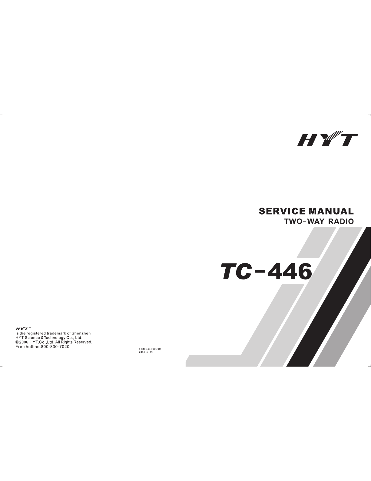
Brief Introduction
(1)
(3)
(4)
(6)
(5)
(7)
(9)
(8)
(2)
(10)
(11)
(12)
(13)
1. Antenna
2. LED indicator
The light will glow red during transmission. The light will glow green during receiving. During
transmission, the light flashes red when the battery voltage is low.
3. Channel selector knob
Turn the channel selector knob to select from channels 1-16 (Channel 16 can be programmed by
your dealer as scan function).
4. Power/Volume control knob
Rotate the Power/VolumeKnob clockwise until a “click”is heard to turn the radio on, fully counter
clockwise until a “click”is heard to turn the radio off. When the radio is on, turn the knob to adjust
volume.
5. PTT key
Press and hold PTT key to talk, release to receive.
6. Monitor key
In receive mode, long press(above 2 seconds) Monitor key to monitor activity on the current
channel.
7. Microphone
8. Speaker
9. External jack
Remove the jack cover and insert an earphone; or insert programming cable into the jack to
programme the radio via programming software.
10. Battery
11. Belt clip
Used to clip radio on your belt.
12. Battery latch
Used to fasten and remove the battery.
13. Charging connectors
Connect the charging connectors with that on the charger to begin charging.
Page 6

TC- 446 Service Manual
- 4 -
Software Specification
Radio Feature Description
1. Use channel selector knob to choose from 15+1(Scan) channels
2. Monitor
3. CTCSS/CDCSS
Non-standard Model (Other): 38+83 groups
4. Channel Spacing
12.5KHz Narrow Optional
5. Channel Scan (Priority channel and scan revert channel available)
6. Battery Save feature (Dealer programmable)
7. Time-out Timer (TOT)
8. Squelch Level Control (9 levels)
9. Low Battery Alert
10. Model Set Mode
11. PC Programming and Adjusting Mode
12. User Wired Clone Mode
13. Factory Wired Clone Mode
14. Manual Adjust Mode
Radio Modes
1. User Mode:
User mode is conventional communication mode. Turn the power on while disconnecting the two SELF points, the
radio enters user mode. (Refer to “TC-446 Owner’s Manual”for details about operation in this mode.)
2. Model Set Mode
(1) If the radio is standard model, short out the two MS2 points on PCB and then operate following the steps (3) (5) and
(6). If the radio is non-standard model, please disconnect the two MS2 points on PCB and then operate the
following steps.
(2) To select MS1 (See the initial data table) according to the radio model, if MS1 is 1, short out the two MS1 points on
PCB and continue the following operation. If not, disconnect the two MS1 points and continue.
(3) Short out the two SELF points on PCB and then turn the power on. Two beeps sound.
(4) Turn channel selector knob to the corresponding position (1-11) according to the radio model (Refer to the initial
data table).
(5) Press PTT key while holding down MONI key to set the model. Channel data and settings are initialized (Refer to
the initial data table).
(6) Turn off the power and then disconnect the two SELF points on PCB to complete the model setting.
Take TC-446 (446.00625~446.09375MHz) as example. From the initial data table, it is of standard model. Toinitializeits
model and channel data, you can operate as following:
(1) Short out the two MS2 points on PCB;
(2) Short out the two SELF points. Power on and two BEEP sounds will be heard.
(3) Press PTT key while holding down MONI key. Channel data and settings are initialized (refer to the initial data table).
Page 7

TC- 446 Service Manual
- 5 -
(4) After data reset, turn off the power, disconnect the two SELF points and restart the power to use the radio.
Remarks: The old data (frequency, CTCSS/CDCSS, channel function settings) will be changed once the model is set,
and part of functions will also be changed. Therefore, do not make this operation unless it’s very necessary, such as
changing the EEPROM, etc.
3. PC Programming Mode
The following parameters can be set through programming software:
(1) Receive frequency and transmit frequency
(2) Receive signaling and transmit signaling
(3) Busy channel lockout
(4) Time-out timer
(5) Squelch level
(6) Battery save
(7) Audio alarm
(8) Monitor mode
(9) Scan mode
(10) Scan revert channel
(11) Priority scan channel
(12) N/W Model
(13) low power
(14) N setting
4. PC Adjusting Mode
The following parameters can be set via PC programming software:
(1) Low battery alert level
(2) Squelch level 9
(3) Squelch level 3
(4) CTCSS deviation (narrow)
(5) CDCSS deviation (narrow)
5. Manual Adjust Mode
If manual adjust mode is enabled, turn on the power while holding down PTT and MONI simultaneously,the radio enters
manual adjust mode after 2 seconds. Choose the adjusting items by turning the channel selector knob to CH1-CH5
position; use PTT (upwards) or MONI (downwards) to adjust (Note: MIC jack shouldn’t be connected with external cable
while adjusting), CH1-CH5 positions are defined as follows:
(1) Low battery alert level
(2) Squelch level 9
(3) Squelch level 3
(4) CTCSS deviation (narrow)
(5) CDCSS deviation (narrow)
Note:
To enable or disable manual adjust mode: short out the two SELF points, turn on the powerto enter model set mode. And
then the manual adjust mode is enabled. Press [PTT], manual adjust mode is disabled. This mode is suggested to be
disabled after the adjustment is completed.
Page 8

TC- 446 Service Manual
- 6 -
6. User/Factory Wired Clone Mode
Turn on the power while holding down MONI, the radio enters wired clone mode.
(1) If the two SELF points are disconnected, press MONI again to begin user wired clone and red LED blinks; When
cloning is completed, red LED goes out.
(2) If the two SELF points are short circuit, press MONI again to begin factory wired clone and red LED blinks; When
cloning is completed, red LED goes out.
Note: The difference between user wired clone mode and factory wired clone mode is that the latter is able to clone
tune parameters.
Page 9
TC- 446 Service Manual
- 7 -
Initial data table
Note: For standard model, CTCSS isoff inall channels after initialization.
MS1 Model
Frequency (MHz) IF (MHz)
1CH 2CH 3CH 4CH 5CH 6CH 7CH 8CH 9-16CH
Tx
(MHz)Rx(MHz)Tx(MHz)Rx(MHz)Tx(MHz)Rx(MHz) (MHz) (MHz) (MHz) (MHz) (MHz) (MHz)
Standard 446.00625~446.09375 -21.4 446.00625 446.00625 446.05625 446.05625 446.03125 446.03125 446.08125 446.01875 446.06875 446.04375 446.09375
CH QT/DQT OFF OFF OFF OFF 97.4 97.4 71.9 79.7 67 85.4 023
Page 10
TC- 446 Service Manual
- 8 -
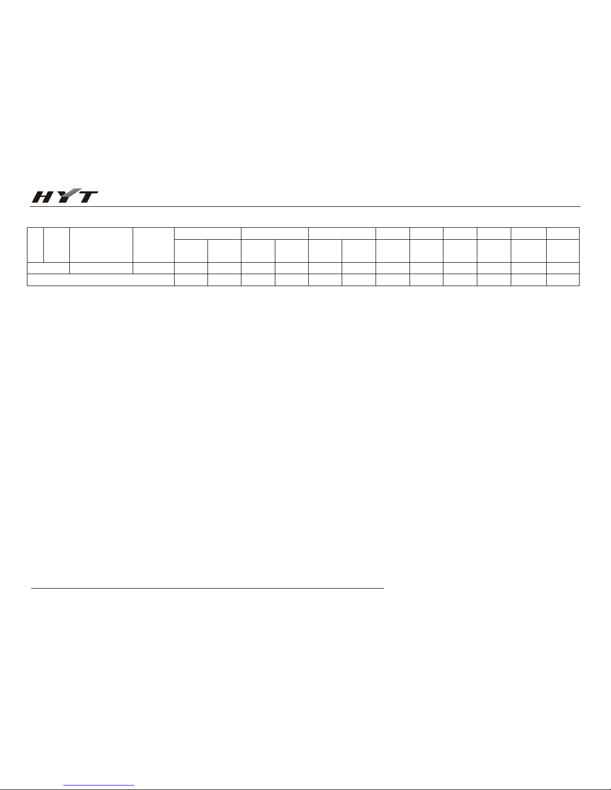
Circuit Description
1. Frequency Configuration
The receiver utilizes double conversion superheterodyne. The first IF is 21.4MHz and the second
is 455KHz. The first local oscillator signal is supplied from PLL circuit. Frequency needed in the
transmitter is supplied from PLL circuit. Figure 1 shows the frequency configuration.
Frequency Range: 446.00625 MHz— 446.09375MHz
Figure 1 frequency configuration
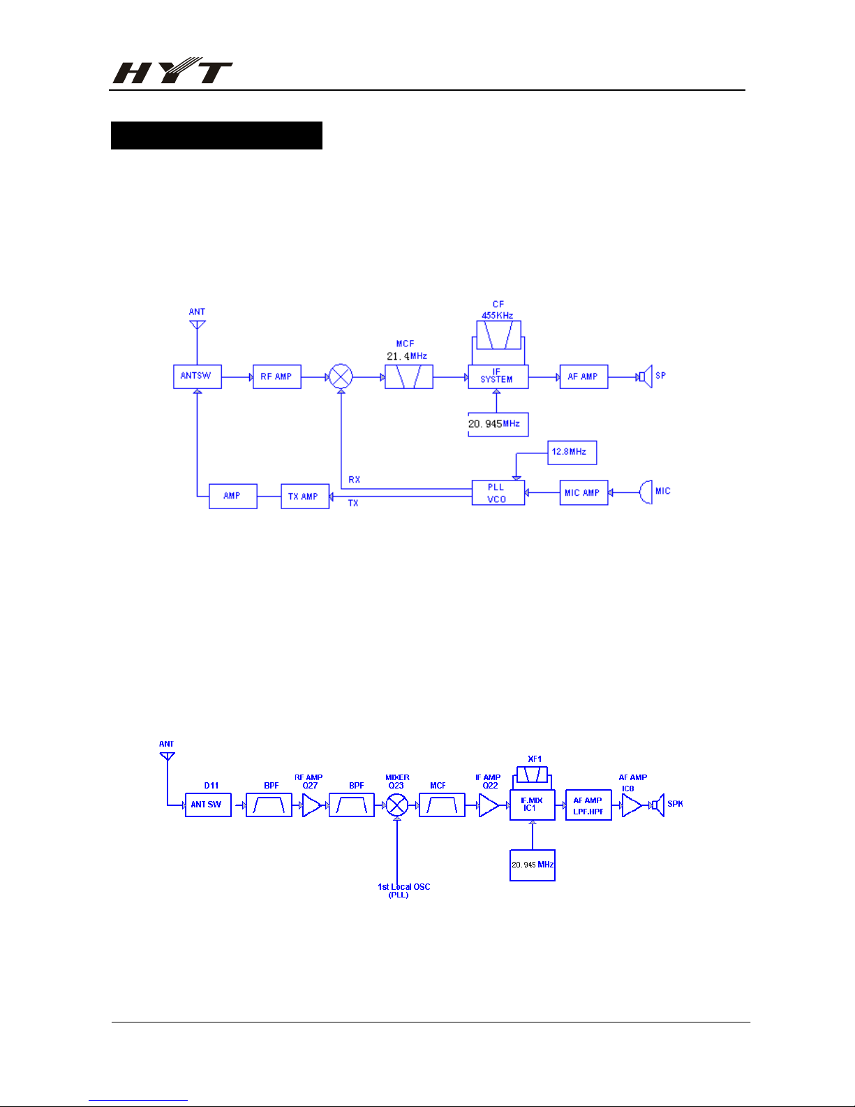
2. Receiver
The receiver utilizes double conversion superheterodyne.
1) Front-end RF Amplifier
The input signal from antenna is amplified in RF amplifier (Q27) after passing through
the receive/transmit switch circuit and a 3-stage LC band pass filter. The amplified
signals are filtered by a band pass filter (a 3-stage LC BPF) to eliminate unwanted
signals before they goes to the first frequency mixer.
Figure 2 receiver section configuration
Page 11

TC- 446 Service Manual
- 9 -
2) The First Mixer
The signal from RF amplifier is mixed with the first local oscillator signal from PLL frequency
synthesizer in the first mixer (Q23) to generate a 21.4MHz first IF signal. The first IF signal is then
fed through two monolithic crystal filters (XF1) to remove spurious signals from adjacent channels.
3) IF Amplifier
The first IF signal is amplified in Q22 and then enters the IF process chip IC1. The signal is mixed
with the second local oscillator signal in IC1 to create a 455KHz second IF signal. The second IF
signal is then fed to a 455KHz ceramics filter (CF1) to eliminate unwanted signals before it is
amplified and FM detected in IC1.
4) AF Amplifier
The demodulated AF signal obtained from IC1 is amplified in IC7 (1/4), and then filtered by low
pass filter Q19 and high pass filter Q20, and then de-emphasized by R130 and C156. The
resulting AF signal passes through a volume control circuit and then is amplified to a sufficient
level to drive the speaker by AF power amplifier (IC8).
5) Squelch
Part of the AF signal from IC1 enters IC1 again, and the noise component is amplified and
rectified by a filter and an amplifier to produce a DC voltage corresponding to the noise level. The
DC signal from IC1 goes to the analog port of the microprocessor (IC11). IC11 determines
whether to output sounds from the speaker by detecting whether the input voltage is higher or
lower than preset value.
To output sounds from the speaker, IC11 sends a high level signal to the MUTE and AFCO lines
and turns IC8 on through Q12.
DET
FM IF IC1
IF AMP
HPF
AMP
IC7
AF
LPF
HPFDET
2
39 40 1
SW
Q12
SW
AF/PF AMP
IC7
LPF
IC11
MCU
BUSY
MUTE
AFCO
TI
IC8
SP
Figure 3. AF amplifier and squelch circuit
Page 12
TC- 446 Service Manual
- 10 -
6) Receivesignaling
CTCSS/CDCSS
Audio frequencies over 300Hz of the output signal from IC1 is cut off by a low-pass filter. The
resulting signal enters the microprocessor IC11. IC11 determines whether the CTCSS/CDCSS
matches the preset value and controls the MUTE and AFCO and the speaker sound output
according to the squelch results.
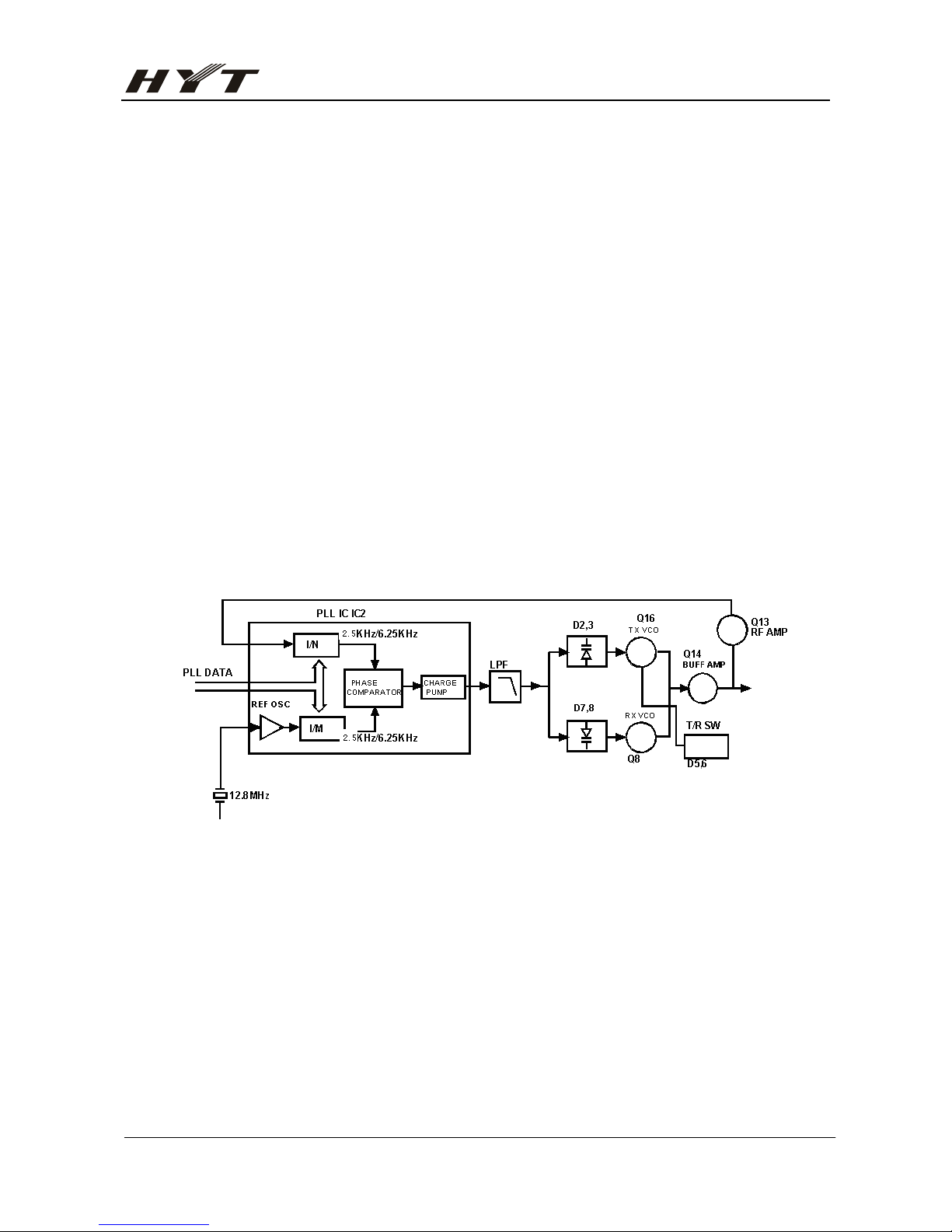
3. PLL Frequency Synthesizer
PLL circuit generates the first local oscillator signal for reception and the RF signal for
transmission.
1) PLL Circuit
The step frequency of PLL circuit is 2.5KHz or 6.25 KHz. A12.8MHz reference
oscillator signal is divided at IC2 by a fixed counter to produce a 2.5 KHz or 6.25 KHz
reference frequency. Output signal from voltage control oscillator (VCO) passes
through buffer amplifier Q14 and is divided at IC2 by the dual-module programmable
counter. The divided signal is compared in the phase comparator IC2 with the 2.5 KHz
or 6.25 KHz reference signal. The output signal from phase comparator is filtered
through a low-pass filter and passed to the VCO to control the oscillator frequency.
(See figure 4)
Figure 4 PLL circuit
2) VCO
The operating frequency is generated by Q16 in transmit mode and by Q8 in receive
mode. The operation frequency generates a voltage through the phase comparator to
control the varactor diodes, so as to keep the oscillator frequency consistent with the
preset frequency in CPU (D2 and D3 in transmit mode and D7 and D8 in receive mode).
T/R pin is set high in receive mode causing Q6 to turn off Q16 and turn Q7 on. The T/R pin is set
low in transmit mode. The output from Q8 and Q16 is amplified by Q14 and sent to the buffer
amplifier.
Page 13
TC- 446 Service Manual
- 11 -
4. Transmitter
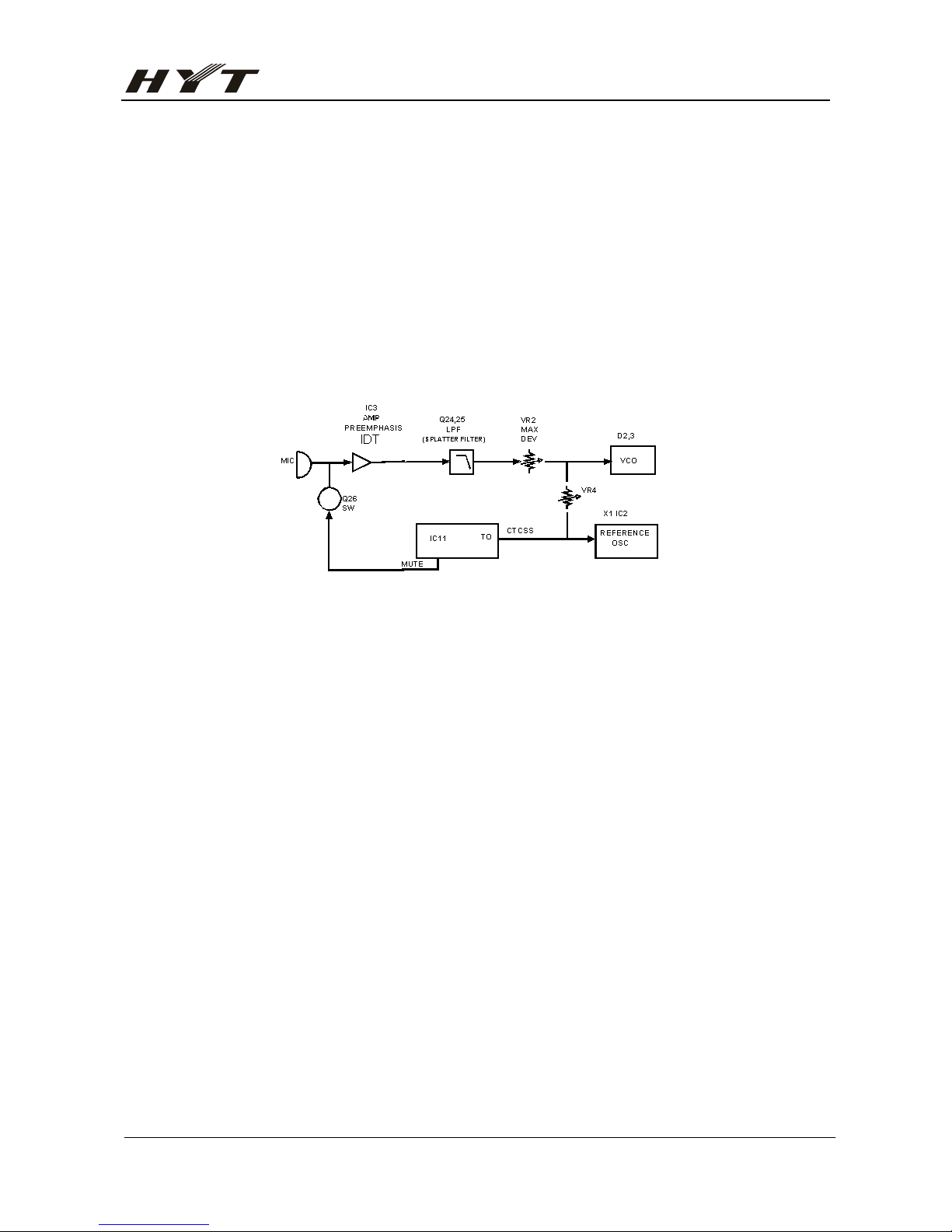
1) Transmit audio
The audio signal from microphone is amplified through IC3, and then pre-emphasized , and
then filtered by another low-pass filter(separate filter)(Q25 and Q24) to eliminate the
frequencies over 3KHz. The resulting signal enters the VCO for direct FM modulation. (See
figure 5)
2) CTCSS/CDCSSEncoder
The necessary frequency for CTCSS/CDCSS encoder is generated by IC11 and
FM-modulated to the PLL reference signal. Since the reference OSC does not modulate the
loop characteristic frequency or higher, modulation is performed at the VCO side by splitter.
(See figure 5)
Figure 5 transmitCTCSS
3) RF amplifier
The transmit signal obtained from VCO buffer amplifier Q14 is amplified by Q15 and Q17.
This amplified signal is passed to power amplifier Q32 and Q31, and is capable of producing
a 4.0W RF power.
4) Antenna Switch and LPF
The RF amplifier output signal is passed through a low-pass filter network and a
transmit/receive switch circuit before it is passed to the antenna terminal. The
transmit/receive switch circuit is comprised of D11 and D12. D11 and D12 is turned on in
transmit mode and off in receive mode.
5. Power
The 5V reference power supply for the control circuit is derived from an internal battery. The
reference power provides a 5V supply in transmit mode [T_V], a 5V supply in receive mode [R_V],
and a 5V supply shared in both modes based the control signal from the microprocessor.
6. Control System
The IC11 CPU operates at 7.3728MHz.
Page 14
TC- 446 Service Manual
- 12 -
CPU Pins
PIN No. PIN NAME I/O DESCRIPTION
1 TI I CTCSS/CDCSS input
2 BUSY I Input busy signal
3 BATT I Detect battery voltage
4 TIBI I CTCSS/CDCSS exterior circuit central point input
5 NC
6 SAVE O Power saving control H: OFF L: ON
7 TXLow O Transmitter power control H: Low power L: High power
8 NC
9 DAT O data output
10 CLK O clock output
11 LE O PLL IC enable
12 BEEP O Beep output
13 SCL O E2PROM clock cable
14 SDA I/O E2PROM data cable
15 MUTE O MIC mute control H: Mic mute L:Mic enable
16 MS1 I Model set
17 GREEN O Green light control H: light
18 RED O Red light control H: light
19 TXD O RS-232C output
20 RXD I RS-233C input
21 PTTK I PTT key input
22 MS2 I Standard model select H: Non-standard L: Standard
23 RXC O Receiver power control L: power on
24 NC
25 RESET I Reset input
26 SELF I Self-program L: on
27 TXC O Transmitter power control H:on
28 X
IN
I Oscillator input
29 X
OUT
O Oscillator output
30 Vss I Grounding
31 R/T O TX/RX control H:RX L: TX
32 UL I PLL unlock detector H: Lock L: unlock
33 IF-SELECT I IF select H: 21.4MHz L: 45.05MHz
34 MONIK I MONI key input
35
ENC0
I Channel selector knob encode input
36 ENC1 I
37 ENC2 I
Page 15
TC- 446 Service Manual
- 13 -
38
ENC3
I
39 AF
MUTE
O Audio muting control
40 AFP O Audio power control
41 TONE5 O CTCSS code output
42 TONE4 O CTCSS code output
43 TONE3 O CTCSS code output
44 TONE2 O CTCSS code output
45 TONE1 O CTCSS code output
46 TONE0 O CTCSS code output
47
WNTC
O W/N L: Wide H: Narrow
47-70 NC
71 Vcc I Power input:5V
72 V
REF
I A-D converse reference voltage
73 Avss I A-D GND
74-77 NC
78 NC
79 NC
80 NC
Page 16

TC- 446 Service Manual
- 14 -
Part List 1
No. P/N Material Name Qty. Ref. No. Address
1 3001051830000 Chip resistor 0402 18KΩ J 1/1 1 R622 B3I
2 3001060000000 Chip resistor 0603 0Ω J 1/10W 16 C23 B3F
3 D20 T1D
4 L3 B3H
5 Q41 T3F
6 R106 T3F
7 R107 B3B
8 R108 B3E
9 R110 T4G
10 R151 B5E
11 R192 B4E
12 R194 B3F
13 R197 B4F
14 R202 B2B
15 R508 B5B
16 R601 B1E
17 R602 B3C
18 3001061000000 Chip resistor 0603 10Ω J 1/10 6 R112 T3E
19 R113 T5J
20 R164 B2C
21 R196 B4G
22 R80 B2D
23 R82 B4G
24 3001061010000 Chip resistor 0603 100Ω J 1/1 6 R127 B5F
25 R147 B4E
26 R74 B2C
27 R75 B4J
28 R76 B5E
29 R90 T5H
30 3001061020010 Chip resistor 0603 1KΩ J 1/10 12 R203 T2E
31 R39 B3B
32 R51 B1F
33 R52 T3F
34 R53 B2D
35 R56 B2B
36 R57 B5B
37 R58 T4B
38 R59 T3B
39 R60 T2D
40 R61 T2D
41 R89 T4I
42 3001061030010 Chip resistor 0603 10KΩ J 1/1 10 R100 T4B
43 R204 T2G
44 R36 B4B
Page 17
TC- 446 Service Manual
- 15 -
Part List 1
No. P/N Material Name Qty. Ref. No. Address
45 R37 T2E
46 R38 B2A
47 R40 B3F
48 R41 T5F
49 R42 T5E
50 R44 B2I
51 R45 B2I
52 3001061040010 Chip resistor 0603 100KΩ J 1/ 15 R10 B4C
53 R12 B4B
54 R13 B3D
55 R15 B3D
56 R175 T2B
57 R176 T2B
58 R18 T2C
59 R35 T2C
60 R623 B4E
61 R624 B4F
62 R625 B3E
63 R626 B3F
64 R7 B4B
65 R8 B2E
66 R9 B1D
67 3001061050010 Chip resistor 0603 1MΩ J 1/10 2 R109 T2B
68 R116 T3B
69 3001061230000 Chip resistor 0603 12KΩ J 1/1 2 R170 B1D
70 R617 B4H
71 3001061240010 Chip resistor 0603 120KΩ J 1/ 3 R11 B3B
72 R124 T3F
73 R72 B2D
74 3001061510000 Chip resistor 0603 150Ω J 1/1 2 R68 B2E
75 R69 B2C
76 3001061520000 Chip resistor 0603 1.5KΩ J 1/ 3 R48 B3E
77 R50 T5F
78 R55 T2E
79 3001061530010 Chip resistor 0603 15KΩ J 1/1 3 R161 T4F
80 R162 T4G
81 R163 T4F
82 3001061540000 Chip resistor 0603 150KΩ J 1/ 5 R139 B4B
83 R14 B3D
84 R140 B4A
85 R141 B4A
86 R142 B4A
87 3001061820000 Chip resistor 0603 1.8KΩ J 1/ 2 R131 T4E
88 R144 B3C
Page 18

TC- 446 Service Manual
- 16 -
Part List 1
No. P/N Material Name Qty. Ref. No. Address
89 3001061850000 Chip resistor 0603 1.8MΩ J 1/ 2 R155 T5G
90 R156 T5F
91 3001062030000 Chip resistor 0603 20KΩ J 1/1 1 R98 B3D
92 3001062220000 Chip resistor 0603 2.2KΩ J 1/ 4 R165 B4F
93 R174 T4H
94 R3 B4B
95 R6 T2B
96 3001062230000 Chip resistor 0603 22KΩ J 1/1 2 R104 B3H
97 R120 T4G
98 3001062240010 Chip resistor 0603 220KΩ J 1/ 2 R145 T5F
99 R167 T1D
100 3001062710000 Chip resistor 0603 270Ω J 1/1 1 R616 T3E
101 3001062720000 Chip resistor 0603 2.7KΩ J 1/ 4 R114 B1B
102 R49 B4D
103 R64 B2G
104 R65 B2G
105 3001062730010 Chip resistor 0603 27KΩ J 1/1 2 R102 B3H
106 R132 B3C
107 3001062740010 Chip resistor 0603 270KΩ J 1/ 2 R16 B3D
108 R2 B3C
109 3001063020000 Chip resistor 0603 3KΩ J 1/10 1 R81 B3F
110 3001063310010 Chip resistor 0603 330Ω J 1/1 5 R122 B3G
111 R146 B4D
112 R5 B4E
113 R67 B2D
114 R96 B2B
115 3001063320000 Chip resistor 0603 3.3KΩ J 1/ 14 R135 B4B
116 R136 B4A
117 R137 B4B
118 R138 B5A
119 R25 B4B
120 R26 B4D
121 R27 B2F
122 R28 B1F
123 R29 B2D
124 R30 B2E
125 R31 B3G
126 R32 B5E
127 R33 T5F
128 R34 B2D
129 3001063330010 Chip resistor 0603 33KΩ J 1/1 1 R24 T2G
130 3001063340000 Chip resistor 0603 330KΩ J 1/ 1 R43 T2A
131 3001063930010 Chip resistor 0603 39KΩ J 1/1 5 R152 T5F
132 R153 T5F
Page 19

TC- 446 Service Manual
- 17 -
Part List 1
No. P/N Material Name Qty. Ref. No. Address
133 R154 T4F
134 R158 T5F
135 R159 T5E
136 3001064700000 Chip resistor 0603 47Ω J 1/10 4 R115 B2A
137 R123 B3G
138 R125 B3H
139 R191 B2B
140 3001064710000 Chip resistor 0603 470Ω J 1/1 4 L1 B4B
141 R118 B2I
142 R166 B4F
143 R62 B2I
144 3001064720000 Chip resistor 0603 4.7KΩ J 1/ 6 R121 T1B
145 R177 T2A
146 R84 B2C
147 R87 T2A
148 R88 T1C
149 R99 T1B
150 3001064730000 Chip resistor 0603 47KΩ J 1/1 13 R101 B4H
151 R103 B4G
152 R105 B1E
153 R128 B3B
154 R4 T2B
155 R54 T3G
156 R606 T3I
157 R607 T3I
158 R608 T3I
159 R609 T3I
160 R610 T2C
161 R615 B3B
162 R93 T2F
163 3001064740010 Chip resistor 0603 470KΩ J 1/ 2 R22 T1D
164 R94 T3F
165 3001065620010 Chip resistor 0603 5.6KΩ J 1/ 2 R130 B4B
166 R79 B2D
167 3001065630000 Chip resistor 0603 56KΩ J 1/1 4 R149 B3E
168 R157 T4F
169 R198 T4E
170 R627
171 3001065640000 Chip resistor 0603 560KΩ J 1/ 1 R148 B4D
172 3001066810010 Chip resistor 0603 680Ω J 1/1 1 R70 B3F
173 3001066820000 Chip resistor 0603 6.8KΩ J 1/ 1 R85 T4F
174 3001066830000 Chip resistor 0603 68KΩ J 1/1 1 R618
175 3001066840000 Chip resistor 0603 680KΩ J 1/ 1 R134 B3C
176 3001067540000 Chip resistor 0603 750KΩ J 1/ 1 R160 T4G
Page 20

TC- 446 Service Manual
- 18 -
Part List 1
No. P/N Material Name Qty. Ref. No. Address
177 3001068200000 Chip resistor 0603 82Ω J 1/10 1 R171 B1D
178 3001068210010 Chip resistor 0603 820Ω J 1/1 3 R47 B4D
179 R619 B4D
180 R66 B1F
181 3001068220000 Chip resistor 0603 8.2KΩ J 1/ 3 R117 B2B
182 R169 B1D
183 R628 T2E
184 3001068230010 Chip resistor 0603 82KΩ J 1/1 2 R133 T2C
185 R97 B3C
186 3001068240000 Chip resistor 0603 820KΩ J 1/ 1 R1 B4B
187 3001080000000 Chip resistor 1206 0Ω J 1/4W( 4 F1 T4G
188 R172 T2H
189 R173 T2I
190 R77 T2H
191 3002994730000 Trimmer resistor 2.7*2.0*1.6 47K 1 VR2 T5E
192 3002996830000 Trimmer resistor(2*2) 68KΩ(+25%) 3 VR3 T4E
193 VR4 T1B
194 VR5
195 3005991030070 Array resistor 0603 10KΩ*4 J 1/ 2 CP1 T1B
196 CP6 T4A
197 3005061030040 Array resistor 0603 10KΩ*2 J 1/ 1 CP5 T1B
198 3005064720000 Array resistor 0603 4.7KΩ*2 J 1 1 CP4 T1B
199 3005064720010 Array resistor 0603 4.7KΩ*4 J 1 1 CP3 T1B
200 3101050100000 Chip capacitor 0402 1PF C 50V 4 C104 B4G
201 C143 B4I
202 C146 B4I
203 C95 B1E
204 3101050200010 Chip capacitor 0402 2PF B 50V 2 C134 B5H
205 C195 B2B
206 3101050300000 Chip capacitor 0402 3PF B 50V 3 C103 B2B
207 C105 B4G
208 C136 B3H
209 3101050400010 Chip capacitor 0402 4PF B 50V 1 C186 B2C
210 3101050500010 Chip capacitor 0402 5PF B 50V 3 C107 B4E
211 C108 B5E
212 C189 B2C
213 3101050590020 Chip capacitor 0402 0.5PF B 50 4 C163 B4F
214 C164 B4G
215 C91 B2D
216 C94 B4E
217 3101050600010 Chip capacitor 0402 6PF B 50V 5 C106 B5E
218 C182 B1D
219 C96 B2D
220 C97 B2E
Page 21

TC- 446 Service Manual
- 19 -
Part List 1
No. P/N Material Name Qty. Ref. No. Address
221 C98 B3G
222 3101050800000 Chip capacitor 0402 8PF B 50V 6 C101 B4I
223 C139 B4I
224 C141 B4J
225 C142 B4I
226 C193 B1D
227 C90 B1E
228 3101051000000 Chip capacitor 0402 10PF D 50V 6 C135 B3F
229 C144 T4F
230 C187 B2C
231 C253
232 C255
233 C88 B2E
234 3101051010030 Chip capacitor 0402 100PF J 50 6 C132 B2D
235 C15 B2A
236 C16 B2A
237 C17 B2A
238 C179 B3C
239 C180 B2A
240 3101051020010 Chip capacitor 0402 1000PF K 5 30 C109 B2C
241 C110 B2C
242 C111 B4H
243 C113 B2B
244 C114 B3H
245 C121 B2E
246 C147 B4I
247 C252
248 C26 B2B
249 C59 B1G
250 C60 B1G
251 C61 B2G
252 C62 B2G
253 C65 B1C
254 C66 T1E
255 C68 B3H
256 C69 B3C
257 C70 B4A
258 C71 B5B
259 C73 B3E
260 C74 B4E
261 C75 T4F
262 C76 T4G
263 C77 T4G
264 C78 T2D
Page 22

TC- 446 Service Manual
- 20 -
Part List 1
No. P/N Material Name Qty. Ref. No. Address
265 C79 T1E
266 C80 T1D
267 C81 T1C
268 C82 B2I
269 C83 B2I
270 3101051030020 Chip capacitor 0402 0.01UF K 2 15 C10 T5F
271 C11 T1B
272 C12 B3I
273 C137 T2I
274 C2 B4B
275 C240 T3J
276 C241 T3J
277 C242 T3J
278 C243 T3J
279 C3 B4B
280 C4 B4C
281 C5 B1F
282 C7 B2C
283 C8 B4A
284 C9 T5F
285 3101051040040 Chip capacitor 0402 0.1UF K 10 15 C178 T2B
286 C233 B4E
287 C246 B3B
288 C250 T3E
289 C37 B4B
290 C38 B4C
291 C39 B4D
292 C40 T2F
293 C43 B3C
294 C45 B5B
295 C46 B3C
296 C50 T4G
297 C51 B3I
298 C64 T2F
299 C84 T2E
300 3101051590000 Chip capacitor 0402 1.5PF B 50 2 C140 B4I
301 C196 B3E
302 3101051810000 Chip capacitor 0402 180PF J 50 1 C18 B5B
303 3101051830000 Chip capacitor 0402 0.018UF K 1 C156 B5B
304 3101052200010 Chip capacitor 0402 22PF J 50V 2 C100 B2D
305 C188 B1C
306 3101052210010 Chip capacitor 0402 220PF J 50 3 C13 B4B
307 C14 B4B
308 C239 T5I
Page 23

TC- 446 Service Manual
- 21 -
Part List 1
No. P/N Material Name Qty. Ref. No. Address
309 3101052220000 Chip capacitor 0402 2200PF K 5 1 C254
310 3101052230000 Chip capacitor 0402 0.022UF K 4 C167 T5F
311 C168 T4G
312 C169 T4G
313 C44 B4B
314 3101052240010 Chip capacitor 0402 0.22UF Z 1 1 C123 B1B
315 3101052490010 Chip capacitor 0402 2.4PF B 50 2 C102 B4I
316 C192 B1D
317 3101052710000 Chip capacitor 0402 270PF J 50 1 C67 B3H
318 3101052720000 Chip capacitor 0402 2700PF K 5 1 C172 T5F
319 3101053300000 Chip capacitor 0402 33PF J 50V 5 C175 T2B
320 C176 T3B
321 C52 B4B
322 C53 B4B
323 C54 B4C
324 3101053320010 Chip capacitor 0402 3300PF K 5 1 C166 T5F
325 3101053330000 Chip capacitor 0402 0.033UF K 5 C150 B4B
326 C151 B4B
327 C152 B4B
328 C153 B4B
329 C160 B3D
330 3101053340000 Chip capacitor 0402 0.33UF K 6 2 C126 B1B
331 C133 B4G
332 3101053900000 Chip capacitor 0402 39PF J 50V 1 C138 B3H
333 3101053920000 Chip capacitor 0402 3900PF K 2 1 C181 T2C
334 3101053930000 Chip capacitor 0402 0.039UF K 1 C122 T2E
335 3101054700010 Chip capacitor 0402 47PF J 50V 1 C55 B3I
336 3101054710010 Chip capacitor 0402 470PF K 50 22 C149 B2G
337 C197 B3B
338 C20 B4B
339 C204 B3F
340 C207 B3F
341 C208 B4J
342 C21 B2E
343 C22 B2D
344 C231 B1C
345 C24 B4G
346 C25 B2B
347 C251 B3E
348 C27 B3G
349 C28 B4H
350 C29 B3I
351 C30 B4I
352 C31 B2D
Page 24

TC- 446 Service Manual
- 22 -
Part List 1
No. P/N Material Name Qty. Ref. No. Address
353 C32 B5E
354 C33 B5F
355 C35 B4F
356 C36 B4E
357 C42 B4G
358 3101054720000 Chip capacitor 0402 4700PF K 5 2 C232 T4F
359 C57 B4D
360 3101054730000 Chip capacitor 0402 0.047UF K 5 C157 T5F
361 C158 T4E
362 C161 T2C
363 C162 B3C
364 C237 T3E
365 3101055610000 Chip capacitor 0402 560PF K 50 2 C171 T5F
366 C34 T5G
367 3101055620000 【switch to 3101055620010】SMT 1 C47 B3D
368 3101057590000 Chip capacitor 0402 7.5PF(±0.1 1 C89 B4I
369 3101058200000 Chip capacitor 0402 82PF J 50V 1 C58 B4C
370 3101060100010 Chip capacitor 0603 1PF B 50V 1 C92 B2C
371 3101060200010 Chip capacitor 0603 2PF B 50V 1 C93 B4E
372 3101060600010 Chip capacitor 0603 6PF B 50V 1 C145 B4J
373 3101061020000 Chip capacitor 0603 1000PF K 5 4 C198 T4G
374 C235 B4J
375 C63 B1D
376 C72 B3D
377 3101061040010 Chip capacitor 0603 0.1UF K 16 4 C194 T4H
378 C48 T4G
379 C49 T4G
380 R200 B2B
381 3101061800000 Chip capacitor 0603 18PF J 50V 2 C19 B5H
382 C506 B3I
383 3101064710000 Chip capacitor 0603 470PF K 50 2 R111 B4E
384 R150 B5F
385 3102992000040 Trimmer capacitor 3.2*2.5*1.25mm 5 TC1 B1D
386 TC2 B1C
387 TC3 B4G
388 TC4 B5F
389 TC5 B4E
390 3104071050020 Ta-capacitor 0805 1UF M 6.3V 6 C124 B1B
391 C200 T4E
392 C202 B3B
393 C85 B1G
394 C86 B1F
395 C87 B2G
396 3104081050000 Ta-capacitor 1206 1UF M 16V T 1 C174 T3F
Page 25

TC- 446 Service Manual
- 23 -
Part List 1
No. P/N Material Name Qty. Ref. No. Address
397 3104081550000 Ta-capacitor 1206 1.5UF±20% 1 1 C112 T2G
398 3104081560030 Ta-capacitor 1206 15UF M 6.3V 2 C115 B2C
399 C177 T1D
400 3104082250030 Ta-capacitor 1206 2.2UF K 16V 1 C165 T5F
401 3104082260040 Ta-capacitor 1206 22UF M 10V 3 C118 T2E
402 C247 T3E
403 C248 T3E
404 3104084750030 Ta-capacitor 1206 4.7UF K 16V 2 C117 B1B
405 C173 T4F
406 3104201070000 Ta-capacitor 2220 100UF M 6.3 1 C203 T5G
407 3104204760020 Ta-capacitor C-packing 47UF M 16V T 1 C120 B2G
408 3210107221000 Framework inductor 0805 220nH LQW2 1 L4 B4J
409 3210108230010 Framework inductor 1206 23nH LQW31 2 L16 B2B
410 L44 B1E
411 3210209102010 Framework inductor 1210 1uH LQH32M 1 L43 B5J
412 3210305150010 Multi-layer inductor 0402 15nH LQG15 1 L21 B3G
413 3210305180000 Multi-layer inductor 0402 18nH LQG15 1 L26 B2B
414 3210305220000 Multi-layer inductor 0402 22nH LQG15 3 L18 B2D
415 L19 B2D
416 L25 B3E
417 3212105101000 Multi-layer inductor 0402 100nH HK10 4 L17 B1C
418 L40 B5E
419 L47 B2C
420 L48 B1C
421 3212105470000 Multi-layer inductor 0402 47nH HK100 2 L39 B5E
422 L45 B2D
423 3212106339000 Multi-layer inductor 0603 3.3nH HK16 1 L29 B3H
424 3213212102000 Multi-layer inductor 1008 1uH NLV25T 1 L50
425 3213212331000 Multi-layer inductor 1008 330nH NLV2 1 L49 B3E
426 3213306102000 Multi-layer inductor 0603 1uH MLF160 1 L14 T4H
427 3213306221010 Multi-layer inductor 0603 0.22uH MLF 1 L41 T2E
428 3213306332000 Multi-layer inductor 0603 3.3uH MLF1 2 L46 B2C
429 L5 B2E
430 3221506601000 Chip ferrite bead 0603 600Ω±2 5 L12 B3G
431 L13 B2B
432 L6 B2D
433 L7 B2D
434 L8 B2A
435 3221507221000 Chip ferrite bead 0805 220Ω±2 1 L11 B3H
436 3221507600000 Chip ferrite bead 0805 60Ω±25 2 L10 B3J
437 L15 B2G
438 3231321050000 Air-core inductor E2 0.32*1.0*5TR 1 L2 B3H
439 3231351630000 Air-core inductor E2-0.35*1.6*3TR 9 L22 B4H
440 L23 B4I
Page 26

TC- 446 Service Manual
- 24 -
Part List 1
No. P/N Material Name Qty. Ref. No. Address
441 L24 B4I
442 L28 B4J
443 L33 B4G
444 L34 B5E
445 L35 B4E
446 L36 B4E
447 L38 B5F
448 3231351640000 Air-core inductor E2-0.35*1.6*4TL 2 L31 B4F
449 L32 B4G
450 3231351680000 Air-core inductor E2-0.35*1.6*8TR 1 L30 B3I
451 3303010500290 Switch diode 1SS372(TE85L.F 1 D18 T4F
452 3303020100020 Switch diode MA2S11100L SS- 2 D25
453 D9 B2C
454 3303020100070 Switch diode MA2Z07700L SOD 1 D11 B4I
455 3303020100080 Switch diode MA2S07700L 1.7 3 D12 B5H
456 D5 B3F
457 D6 B3F
458 3303030100010 Switch diode DAN222(TL) SOT 1 D19 T4G
459 3303210200000 Switch diode MA2S37600L SS- 4 D2 B2E
460 D3 B2D
461 D7 B1C
462 D8 B1C
463 3307110100080 LED KPT-1608SGC ultra-high 1 D22 T3J
464 3307110100070 LED KPT-1608SRC ultra-high 1 D24 T3J
465 3399990000160 Varactor MA2Z36000L 30V 1 D4 B1D
466 3399990000220 Diode UDZ3.0B SOD-323 1 D10 B2B
467 3401001000080 Transistor 2SA1362-ER(TE85. 1 Q40 T3F
468 3401002000990 Transistor 2SC5108-Y(TE85L. 3 Q13 B2B
469 Q14 B2D
470 Q22 B4D
471 3403007000000 Transistor DTA114EE(TL) PNP 1 Q10 B4D
472 3403007000020 Transistor DTA114YE(TL) PNP 2 Q34 T2B
473 Q9 T2B
474 3403008000010 Transistor DTC114EE(TL) NPN 3 Q28 B2J
475 Q30 B2J
476 Q35 T2B
477 3403008000070 Transistor DTC144EE(TL) NPN 2 Q12 T2F
478 Q39 T2F
479 3403009000010 Transistor UMG3N(N-TR) NPN 2 Q1 B1F
480 Q2 B2F
481 3404002000000 Transistor PRF957 NPN PHILI 1 Q16 B1D
482 3406001000090 Transistor 2SC4988FRTR-E NP 1 Q17 B3G
483 3408002000030 Transistor 2SC4226-R24-A NP 1 Q15 B2D
484 3411002000020 Transistor 2SC5343EG NPN AU 6 Q18 B2D
Page 27

TC- 446 Service Manual
- 25 -
Part List 1
No. P/N Material Name Qty. Ref. No. Address
485 Q19 B4A
486 Q20 B4A
487 Q24 T5F
488 Q25 T5F
489 Q26 T4G
490 3499000000140 Transistor 2SK508-K52-T1B-A 1 Q8 B2C
491 3499000000150 Transistor UMC4(NTR) NPN/PN 1 Q7 B1D
492 3499000000180 Transistor UFMMT717 PNP SOT 2 Q4 B1F
493 Q5 B1F
494 3501020000030 FET 3SK318YB-TL-E-Q 2 Q23 B3E
495 Q27 B5E
496 3503010000010 FET 2SJ243-T1-A P-c 1 Q6 B1C
497 3503020000010 FET 2SK1588-T1-AZ N 1 Q41 T3F
498 3503020000030 FET 2SK1824-T1-A N- 3 Q21 B5B
499 Q46 B2E
500 Q50 B4I
501 3503040000000 FET UPA572T-A N-cha 1 Q3 B2G
502 3504990000010 FET RD01MUS2-T113 P 1 Q32 B3G
503 3504990000020 FET RD07MVS1-T112 P 1 Q31 B3I
504 3602028004610 AF amplification IC KIA6278F-EL/P 1 IC8 T3E
505 3603002005440 IF processing IC TA31136FNG(EL 1 IC1 B4C
506 3603008005040 Operational amplifier NJM2902V 4 OA J 1 IC7 B3C
507 3604002055090 PLL TB31202FN-EL(ELP 1 IC2 B2A
508 3605008005010 Operational amplifier NJM2100V 2 OA J 1 IC3 T4F
509 3608015000000 Power managing IC (voltage regulator) XC6201P5 1 IC4 T1D
510 3609004005280 Reset IC PST9140NR MITSU 1 IC9 T2A
511 3610045000040 SCM M38223M4A-137HP# 1 IC11 T3C
512 3612031004400 Memory AT24C08AN-10SU-2 1 IC5 T5B
513 3701012850010 TCXO 12.8MHz NSA0 1 X2
514 3701737230020 Crystal 7.3728MHz DSX530G 1 X3 T3B
515 4100500101600 TC-500US(U) PCB FR4 1
516 3104081060080 Ta-capacitor 1206 10UF M 10V 4 C1 B4B
517 C125 B4F
518 C155 B4A
519 C159 B3B
Page 28

TC- 446 Service Manual
- 26 -
Adjustment Description
The radio can be adjusted with PC programming software or by manual adjustment. Manual adjustment
procedure of TC-446 is as follow. (Refer to “model set mode”and “manual adjust mode”in the section
Software Specification.)
Instrument:
Radio CommunicationTestSet 1 set
Scanner 1 set
3A/10V Power Supply 1 set
Digital Voltmeter 1 set
3AAmmeter 1 set
Adjustment:
1. Initializing:
It’s necessary to set the model and initialize the radio before alignment because there is no needed
information in EEPROM when the radio is manufactured. Please refer to the “model set mode”in
the section Software Specificationfor details.
2. Adjustment:
Some items can be adjusted in conventional communication mode and the others in manual adjust
mode. Turn on the power, the radio enters conventional communication mode. If manual adjust
mode is enabled, turn on the power while holding down PTT and MONI simultaneously, the radio
enters manual adjust mode after 2 seconds. (Refer to the section Software Specification.)
VCO
Item Condition
Measurement Adjustment Specification
/RemarksTest Instrument Terminal Part Method
1.Power supply 1.power voltage DC 6V
2.Transmit VCO
lock voltage
1.TX High. Turn to CH15 in
manual adjust mode and press
PTT.
Digital Voltmeter CV
TC1
2V±0.1V V
2.TX Low. Turn to CH14 in
manual adjust mode and press
PTT.
2V±0.1V
3. Receive
VCO lock
voltage
1.RX High. Turn to CH15 in
manualadjust mode.
TC2
2V±0.1V
2.RX Low. Turn to CH14 in
manualadjust mode. 2V±0.1V
Page 29

TC- 446 Service Manual
- 27 -
RECEIVER: (Enter the manual adjust mode)
Item Condition
Measurement Adjustment
Specification
/Remarks
Test
Instrument
Terminal Part Method
4.
Band Pass
Filter
1.RX Center. Turn to
CH13 in manual adjust
mode.
Scanner ANT . TP2
TC3
TC4
TC5
Adjust the waveform to the
top, and the top is flat,
the
bandwidth is about 100k
Hz,
the sign of RX central
frequency is at the
of the waveform.
5.sensitivity
1.RX Center. Turn to
CH13 in manual adjust
key to switch N/W).
Radio
Communicati
on Test Set
-
118dBm
MOD:1K
±1.5kHz
(Narrow)
FILER:
0.3-3.4kHz
ANT
Speaker
Jack
Check
SINAD: 12dB or
higher
2. RX Low. Turn to
CH14 in manual adjust
mode (
key to switch N/W).
3.RX High. Turn to
CH15 in manual adjust
mode (
key to switch N/W).
6.Squelch
1.RX Center. Turn to
CH2 in manual adjust
mode. Adjust by
pressing PTT or MONI.
Radio
Communication Test
Set
SSG output
-117dBm
ANT
Speaker
Jack
Level 9
Adjust to just close the
squelch.
Adjustsquelch
level 9
2.RX Center. Turn to
CH3 in manual adjust
mode. Adjust by
pressing PTT or MONI.
Radio
Communication Test
Set
SSG output
-125dBm
Level
3
Adjust to
squelch.
Adjustsquelch
level3
Page 30

TC- 446 Service Manual
- 28 -
Transmitter
Item Condition
Measurement Adjustment
Specification
/Remarks
Test
equipment
Terminal Parts Method
7.Transmit
frequency
1. TX Center. Turn to CH13 in
manualadjust mode and press
PTT.
Radio Communication
Test Set
ANT TC6
Adjust it to center
frequency
Error
≤±250Hz
8.Max.
Deviation
1. Turn to CH13in manual
adjustmode and press PTT
(long press MONI key to switch
N/W).
Radio Communication
Test Set
LPF: 15kHz
AF:1kHz 120mV
MIC Jack
VR2
Adjust deviation to:
2.0kHz±200Hz
(narrow)
Sensitivity
1. Turn to CH13 in manual
adjustmode and press PTT
(long press MONI key to switch
N/W).
Radio Communication
Test Set
FILTER:
FILER:
0.3AF:1kHz 12±2mV
MIC Jack
Check deviation:
1.5±0.15 kHz(narrow)
10. CTCSS
Balance
1. CTCSS: 67.0Hz. Turn to
CH4 in manual adjust mode.
Radio Communication
Test Set
HPF: 20Hz
LPF:300Hz
ANT VR3
Adjust VR3,
tested on condition 1 and
condition
consistent, the difference
≤200Hz
67.0Hz
CTCSS
2. CTCSS: 250.3Hz. Turn to
CH16 in manual adjust mode
and press PTT.
250.3Hz
CTCSS
11. CTCSS
Deviation
1. TX Center. Turn to CH4
(wide) and CH4 (narrow) in
manual adjust mode. Adjust by
pressing PTT or MONI.
Radio Communication
Test Set
HPF: 20Hz
LPF:300Hz
ANT
Adjust deviation to
:
0.4kHz±100Hz(Narrow)
12. CDCSS
Deviation
1. Turn to CH5 (wide) and CH7
(narrow) in manual adjust mod
Adjust by pressing PTT or
MONI.
Adjust deviation to
:
0.4kHz100Hz(Narrow)
13. low
Power
power voltage DC 6V
Radio Communication
Test Set
ANT 500±200mW
14.
Low Battery
Alert Level
1. Turn to CH1 in manual adjust
mode. Adjust the power supply
voltage at 5.3V.Adjust by
pressing PTT or MONI.
Digital Voltmeter
Adjust the level to make
LED just flash.
Note:In manual adjust mode, when channel selector knob is positioned at channel 1-channel16, MIC jack can’t connect with external cables. After
adjustment is completed, short out the two SELF points and then turn the power on, the radio enters model set mode. Then press PTT to disable
the manual adjust mode.
Page 31

TC- 446 Service Manual
- 29 -
TC500 Series Troubleshooting Chart
I. Receiver:
1. No receive or low RX sensitivity / intermittent RX output:
N
Y
N
- Y
N
Y N Y
N
N
Adjust TC3, TC4, TC5; Check
TC3, TC4, TC5, C94, C93,
C106, C163, C164, C105;
Inject 21.4MHz
signal into Q22 pin
C; SSG output ≤
-92dbm;Audioheard
Inject 21.4MHz
signalinto XF1 IN;
SSG output≤
-103dbm; Audio
Check
CF1(455K2nd IF
filter), IC1(IF IC),
X1(20.945M 2
nd
LO),
CD1(demodulator);
CheckXF1 (1
st
IF filter),Q22;
Replacefaulty
components.
signal into
Q27(RF AMP)IN;
SSG≤-113dbm;
Power
supply at
Q9(5R) OK?
Check Q23
(mixer),
Q27, Tc5;
Replace
no-solder joint
at IC11 pin
23; Check
Q9; Replace
faulty
components.
signal into
antenna (wide:
SSG≤
-118dbm,narrow:
SSG≤-116dbm);
Page 32

TC- 446 Service Manual
- 30 -
Repair Example:(Tested by communication test set after power on)
1) Symptom:TX OK; no RX at all, but RX frequency OK; no-solder at one end of crystal X1;
Cure: touch up X1
2) Symptom:TX OK; low RX sensitivity or intermittent RX output;
Cure: replace 455KHz filter
3) Symptom:TX OK; low RX sensitivity, but sensitivity OK after injecting 45.05MHz signal into XF1;
Cure: adjust TC3, TC4, and TC5 in turn
2、No RX audio output(no audio from SPK, sound abnormal):
Symptom 1: no audio after power on/no or low audio in monitor mode:(activate power-onalert tone
and monitor features)
Page 33

TC- 446 Service Manual
- 31 -
N
N Y
N Y
Y N
N Y
N Y
N
Start
Turn to max. VOL; Hold down
MONI; around 2.8V (limit) audio
output at SPK plug?
Check SPK plug,
SPK, spring;
Replace faulty
components;
1 KHz audio input at
IC8(AF AMP) pin1?
Check VR1 and its wiring to IC8;
Replace faulty components.
Hold down MONI;
6V voltage at IC8
pin8?
Hold down MONI; 5V
output at IC11 pin40
(AVP)?
Audio output
at IC8 pin 7?
Check if Q39
and Q12
conductive;
Replace faulty
components.
Check C203, c239;
Replace faulty
components.
See control
section
troubleshooting
Check R203, R37, C84,
C66;
Check IC8 and peripheral
components; Replace
faulty components.
Q41
conductive?
Page 34

TC- 446 Service Manual
- 32 -
Symptom 2: audio OK after power on, no RX audio output or audio distortion in RX (abnormal noise
output while holding down MONI)
Y
N
Y
Y N
N
Y N
Repair Example:
1) Symptom: Hold down MONI, MONI LED glows but no noise output (no RX audio), SPK resistance
OK; 6V measured at Q40 IN, but no 6V output while holding down MONI;
Cure: replace Q40(2SA1362)
2) Symptom: Hold down MONI, 6.0V voltage at IC8 pin8 but no audio output at pin7;
Cure: replace IC8
Start
Hold down MONI;
Audio output at
IC7 pin1?
Check if Q21
conductive; Check
operating status of
Q19, Q20; Check C44,
C150, C151, C152,
C153, C45; Replace
faulty components.
Hold down MONI;
Audio output at IC7
pin3?
5V voltage at
5V voltage at
IC1(IF) pin4?
Check IC7, IC11,
peripheral
components;
Replace faulty
components.
Check the components
betweenQ9 and IC11 pin
23. Replace faulty
components.
Check the wiring
betweenIC1 pin4
and Q9;
Check IC1, CD1 (C24
demodulation), peripheral
components; Replace
faulty components.
Page 35

TC- 446 Service Manual
- 33 -
II. Transmitter:
1、No power (low output power)
Y
Y N
Y
Y
N
.
N
Y
Start
Plug into standard power
supply (7.5V); Connect
instruments; Toggle on
TX; Observe
current&power changes.
Low current
and no power
output in TX
High current but
no or low power
output in TX
In TX, 6.0V
source voltage
at Q31?
In TX, around
1.1W power at
D11positive end?
In TX,
1.8~2.5 V
gate voltage
at Q31?
Check Q32, Q17,
Q38, peripheral
components;
Replace faulty
components.
source voltage
and 1.8~2.5V
gate voltage at
Q32?
Check C30,
C139, C142,
C141, C145;
Replace faulty
components.
Check D11,
R75, C208,
L4
Check bias
circuit;
Replace
Q31;
Check L3,
Q31, C55;
In TX, around 1.1W
power at D11
negative end?
Page 36

TC- 446 Service Manual
- 34 -
N
.
Y
N
Y
N
Y
否
Y
Replace faulty
components;
Check bias
resistor and
TX 5V power
supply circuit.
Replace faulty
components;
C207
OK?
Replace faulty
components;
C23 parameters
and D5 positive
bias OK ?
Replace faulty
components; Check
bias circuit.
4V collector voltage,
1.8V base voltage
and 1V emitter
voltage at Q15?
Check R80,
L18, R34,
R29, R79,
OK ?
Replace with
components of
the same spec;
See VCO
Troubleshootin
R122, C98, R196,
C42 R195 OK?
In TX, 4.8V
collector voltage,
1.2V base voltage
and 0.3V emitter
voltage at Q17?
L29, C138,
C67 OK?
Y
Y
Y
Y
Y
N
Page 37

TC- 446 Service Manual
- 35 -
Repair Example:
1) Symptom: no TX power; > 3ATX current;
Cure: replace Q31
2) Symptom:low TX power; Voltage at Q4, Q31, Q32 OK; 10mw power at Q31(RD07)IN; Around
1W power at D11;
Cure: replace Q31
2、No or low TX audio (test port for communication test set:AF OUT/AF IN)
N
Y
N
Y
是 N
Y N
Y N
Start
Inject 1KHz/100mv AF
signal into MIC plug;
± 4.2KHz ± 150Hz
modulation deviation?
Check MIC
plug and MIC;
Replace faulty
Waveform input at
IC3(NJM2100V)
pin2 OK?
Check L14, C48, C169,
C168; Replace faulty
components.
In TX, amplified
waveform output at
IC3 pin7?
In TX, 5V
voltage at IC3
In TX, waveform
output at VR2?
Check IC3 and
peripheral
components;
Check the
connection to
Q4 C pin.
Check components between
VR2 and VCO (e.g.L10, R22,
C40); replace faulty
components;
Check Q24, Q25, VR2
(47K) and peripheral
components;
Page 38

TC- 446 Service Manual
- 36 -
Repair Example:
1) Symptom: no TX audio, cracked VR2;
Cure: replace VR2 and adjust
2) Symptom: low TX audio; poor modulation sensitivity of MIC after adjusting VR2
Cure: replace MIC
II. PLL:
1、 TX or RX unlock:(Caused by faulty oscillator loop)
Page 39

TC- 446 Service Manual
- 37 -
Y
Y
Start
Correct software mode settings and freq range?
TX unlock: TX unlock on
some channels?
RX unlock: RX unlock on
some channels?
No TX CV
or<0.8V?
Check synthesized
sector;
Bias (pinC 4V)
AdjustTC1;reliable
solder&correct
parametersofC182,
C193, C95,L44,
C192, C90,L5,D4?
AdjustTC2;reliable
solder&correct
parametersofC186,
C187, L46,R69,
L16,C19,C188,
L48,D8,D7,L17?
Check synthesized
sector;
or<0.2V?
Bias (pinC 4V)
4.1Voutput
Reliablesolder andcorrect
parametersofR164,R9,L47,Q8?
IC11pin31?
CheckIC11,
peripheral
components;or
Reliable solder
at Q7, R53; No
disconnected
wiringto branch
circuit?
4Voutput
voltageat
Q6?
Reliablesolder at
R171? No
disconnectedwiringto
IC11pin31?
Reliablesolder atPTT?
Nodisconnectedwiring
toIC11branchcircuit?
Check the value and soldering
of Q6、R9. Replace faulty
components.
CheckR11,L19,R74,Q13;
Replacefaultycomponents.
Voltage at
TX CV?
Voltage at
RX CV?
Adjust TC2
Adjust TC1
Adjust to freq band/freq
set in the radio;
N
Y
N N
Y
N
Y
Y
N
No RX CV
Y
Y
Y
Y
N
Y
Y
Y
Y
Y
N
Y
N
N
Page 40

TC- 446 Service Manual
- 38 -
1、 TX and RX unlock:(Caused by faulty common sector)
Y N
N Y
N Y
N
N
Y
Start
Correct software mode settings and freq range?
Adjust to correct software
mode and freq;
4.9V at IC2 pin2 ?
5V output at
Q5(5C)?
Check L13, R191, C113,
C117, C123; Replace faulty
components.
In
non-battery-sa
ve mode, 5V
(H level) at
IC11pin6 ?
Bad soldering joints
at IC11 pin6?
Correct software
settings? If not,
replace IC11.
Check Q3, R65,
Q2, R28, R66;
Replace faulty
12.8MHz at IC2
pin13?
Check 12.8MHz
crystal, C130, TC6;
Replace faulty
After amplified by Q13,
VCO output
Check VCO
circuit
Data, clock, strobe
pulse at IC
2
pin8/9/10
OK?(triangle wave)
Check CP6, CPU, C15,
C16, C17 and wiring;
1-4V CV control
voltage (output)?
Check the soldering and value of
the components between IC2 pin 3
to CV. Check the soldering of IC2.
Replace faulty components.
High level at D13positive end ?
N
Y
Y
Y
Y
N
Page 41

TC- 446 Service Manual
- 39 -
Repair Example:
1) Symptom:unable to transmit even if PTT is pressed; wrong freq band found when reading from radio
via PC;
Cure: correct the freq band
2) Symptom:unable to lock freq, TR accessible sometimes, occasional TX or RX unlock;
Cure: replace Q15(5108)
3) Symptom: unable to transmit even if PTT is pressed; freq range found OK when reading from radio
via PC; no 5V output at Q5;
Cure: replace Q5(717)
4) Symptom: unable to transmit even if PTT is pressed; freq range found OK when reading from radio
via PC; 5V output at Q5; 5C voltage at X2 (12.8 crystal oscillator);
Cure: replace X1
5) Symptom: able to transmit when PTT is pressed; freq range found OK when reading from radio via
PC; 5C voltage OK; Voltage found at CV in RX but not within 0.8~4V;
Cure: adjust TC2 to make CV within normal range
6) Symptom: Power-on OK; unable to lock freq when pressing PTT, TR accessible sometimes,
occasionalTX or RX unlock;
Cure: replace Q15(5108)
Page 42

TC- 446 Service Manual
- 40 -
VI. Power Supply:
Fail to power on (no response while rotating power knob after plugging in power supply)
N
Y
Plug positive end of power cable into
positive connector while negative end
into aluminum chassis or ground
around PCB;
Turn off radio; 6.0V
output at L15
Upper?
Check L15, C149,
C120; Replace faulty
components.
Switch on power;
6.0V at IC4 IN?
Check power switch,
D20, IC4; Replace
faulty components.
5V at IC4
Check if short circuit
occurs when IC4, C80,
C79, branch circuit are
grounded; Replace
faulty components.
Check IC11 pin 71/ 72;
5V at IC9 pin 5 (RESET)?
Check if no-solder at
IC11and branch
components; Replace
Start
Check IC11, X3 (7.3728
MHz crystal), peripheral
R&C; Replace faulty
Y
N
N
N
Y
Y
Page 43

TC- 446 Service Manual
- 41 -
Repair Example:
1) Symptom: Plug in 6.0 power cable, rotate power knob but unable to switch on power; voltage at L15
OK; no 7.5V at IC4 IN; power knob OK;
Cure: replace D20
2) Symptom: Plug in 6.0 power cable, rotate power knob but unable to switch on power; Voltages at
L15, IC4 IN OK; no 5V (5M) voltage at IC4;
Cure: replace IC404
3) Symptom: Plug in 6.0 power cable, rotate power knob but unable to switch on power; 5V output at
IC4; Voltage at IC9 OK;
Cure: replace X3 (7.3728MHz crystal)
Page 44

TC- 446 Service Manual
- 42 -
Disassembly and Assembly
Remove the Battery
1. Turn the radio off.
2. Slide the battery latches upwards.
3. Pull the top part of the battery away from the radio’s body and lift the battery from the radio.
(See figure 1)
Figure 1
Disassemble main unit (aluminum chassis and PCB)
1. Remove the two screws at the base of the chassis.
2. Pull the volume knob and selector knob off.
3. Remove the antenna at top of the radio.
4. Remove the screw of the microphone jack cover and pull the jack cover off. (See figure 2)
Figure 2
Page 45

TC- 446 Service Manual
- 43 -
Pull the chassis upwards and then pull the chassis away from the front cover. (See figure 3)
Figure 3
The disassembly is shown as the figure 4.
Figure 4
Disassemble PTT button
Push the PTT button in indicated direction until out of the cover. (See figure 5)
Figure 5
Page 46

TC- 446 Service Manual
- 44 -
Assemble PTT button
Paste double-coated tape to the cover.And then press the PTT button into the corresponding opening in
the cover. (See figure 6)
Figure 6
Attach the battery
1. Fit the extensions at the bottom of the battery into the slots on the radio chassis.
2. Press the top part of the battery towards the radio until a click is heard. (See figure 7)
Figure 7
Page 47

TC- 446 Service Manual
- 45 -
Exploded View
1
7
6
8
16
15
10
11
9
18
21
19
22
23
13
14
17
20
24
25
26
27
28
29
30
31
32
33
34
35
36
37
38
39
2
4
3
5
12
Page 48

TC- 446 Service Manual
- 46 -
Part List 2
No. P/N Description Qty.
A 7102506000020 Machine screw M2.5*6.0mm 1
B 7102004020050 Self-tapping screw ST2.0*4.0mm Cross recess pan head (color zinc plating) 11
C 7102009001000 Machine screw M2.0*9.0mm (color zinc plating) 2
D 7102505000100 Machine screw M2.5*5.0mm T9 hexagonal head 2
1 6000051000010 TC500 Rear cover Black ABS700 1
2 6000374000000 TC308 Antenna cap Black TPUS95A 1
3 6100237000000 TC366 Antenna housing Black 85 degree TPU 1
4 7400018000000 TC446 PVC piece at main unit front case antenna hole 1
5 7000014000000 TC2110 Antenna core Ф 3.60mm (red copper plating)
1
6 6300007000030 TC446 Aluminum chassis Grinding ADC12 1
7 7500114000000 TC500 Cooling pad 2.00mm-thick Gap Pad1500 8.0*6.6mm
1
8 6100034000000 TC-500USWater-proof gasket Black 40 degree high-tensile silica rubber 1
9 7500013000000 TC2100 Positive electrode piece water-proof sponge 1.5mm-thick EVA 1
10 6201030000000 TC-500 Battery positive electrode piece 0.20mm SUS301 (nickel plating) 1
11 6000046000000 TC2100 Positive electrode piece support Black ABS 1
12 7207002200000 Nut M7.0*2.2mm 1
13 4303020000030 Volume switch TC-1688 1
14 7206002500010 Nut M6.0*2.5mm 1
15 4302030000010 Channel switch TC-368 RY-6933 tocos 1
16 4301040000020 PTT switch TC-278/TC-378 SKHLLBA010 ALPS 2
17 7400034000000
TC370 Speaker insulating pad 1.0mm-thick EVA Φ 17mm single-side
self-adhesive tape 1
18 5001010000020 Speaker 426539(036S23) 4Ω 0.5W D:36mm FOSTER 1
19 6000160000040 TC-368S Volume knob Black PC+ABS 1
20 6000158000040 TC-368S Channel knob Black PC+ABS 1
21 6201006000000 TC2088 Inner liner (knob) 0.25mm SUS304 2
22 6000050101000 TC500 Main unit front case Black HYTABS700 1
23 6100030000010 TC-500 PTT key Black 60 degree silica rubber 1
24 7400016000000 TC500 Mic mesh Unwoven cloth 0.3mm-thick Φ5.0 1
25 6000189000000 TC3000 Light guide Transparent PMMA 1
26 6000054000000 TC500 Mic cover Black ABS 1
27 7400075000000 TC500 Speaker mesh Unwoven cloth 0.05mm-thick Φ36 1
Page 49

TC- 446 Service Manual
- 47 -
28 6100075000000 TC-368 Mic gasket Black 30 degree silica rubber
1
29 5002110000030 Mic CZII-64AP-RoHS -60dB±2dB φ9.7*4.5mm 1
30 4210080000000 Lead with tin on both ends 80mm Black
1
31 4210080000300 Lead with tin on both ends 80mm Red 1
32 5205000000280 Speaker jack HSJ1456-010320 1
33 5205000000190 Earpiece jack HSJ1650-010020 1
34 7400133000000 TC500 PVC water-proof gasket PVC 0.3mm-thick Φ4.7 2
35 7500115000000 TC500 Battery contact pad Silica rubber 4.8*4.2mm 2
36 6201022000000 TC2100 Battery negative electrode piece 0.20mm SUS301 (nickel plating) 1
37 7400014000010 TC-500 Battery water-proof PVC piece 0.2mm-thick PVC 18.40*16.10mm 1
38 6000039000000 TC2108 Battery latch Black PC+ABS 1
39 7000015000000 TC500 Latch spring Ф 3.00×7×Ф0 .35mm 1
Page 50

TC- 446 Service Manual
- 48 -
Packing
Page 51

Page 52

Page 53

1 2 3 4 5 6 78
A
B
C
D
8
7654321
D
C
B
A
MODEL
FILE NO. REV
HYT Science & Technology Co. Ltd.
Part Name
DRAWN BY CHECKED
APPROVAL
PAGE
OF
DATE
Error : HYT.jpg file not found.
M38223M4H
1
20
40
60
80
IC11
B+
POWER1
9
10
AF
FILO
678
QUAD
FILI
11
IFO DEC
1213141516
54321
OSCI
OSCO
MIXO
VCC
IFIRSSI
NDET
NRECEMIXI
IC1
TA31136FN
C1
10u/10V
C2
0.01u
R1
680K
C13
220PR32.2K
C14
220P
R7
100k
C18
27P
C20
470P
R25
3.3K
C37
0.1U
OUT
IN
CF1
C52
33P
X1
20.945MHz
C53
33P
C3
0.01U
R36
10K
L1
470
R26
3.3K
C57
4700p
C58
82P
CD1
R47
820
C4
0.01U
C38
0.1U
C54
33P
IF
SYSTEM
Q1
UMG3N
Q2
UMG3N
Q3
UPA572T
Q4
FMMT717
Q5
FMMT717
C59
1000P
R51
1K
R27
3.3K
R28
3.3K
C60
1000P
C5
0.01u
R64 2.7K
R652.7K
C87
1u/ 6.3V
R52
1K
C61
1000P
C62
1000P
R66
820
L5
3.3U
D2
MA2S376
D3
MA2S376
C88
10p
L6
601S
C90
7P
D4
MA360
TC1
10P
C182
6P
C193
8P
R67
330
C91
0.5P
C96
6P
C100
22P
C97
6P
D5
MA2S077
R70
680
C103
3P
C63
1000P
Q6
2SJ243
Q7
UMC4
R105
47K
D7
MA2S376
C19
18P
Q8
2SK508NV
R8
100K
R9
100K
R53
1K
L7
601s
TC2
10P
L16
23nH
C189
5P
C186
4P
L48
100N
R72
120K
R74
100
R29
3.3K
R79
5.6K
C21
470P
R68
150
C22
470P
L18
22n
L19
22n
R80
10
R30
3.3K
D6
MA2S077
R31
3.3K
C24
470P
R82
10
R69
150
C92
1P
C7
0.01U
C109
1000p
D9
MA2S111
R84
4.7K
C110
1000p
C115
15u/6.3V
L17
100n
C65
1000P
D8
MA2S376
Q9
DTA114YE
R10
100K
Q10
DTA114EE
C39
0.1U
R113
10
R114
2.7k
R115
47
R117
8.2K
C124
1u/6.3V
L8
601s
C25
470P
R56
1K
Q13
2SC5108
R11
120K
R38
10K
TP1
Q14
2SC5108
Q15
2SC4226
Q17
2SC4988
Q18
2SC5343(s)
C98
6P
C42
470P
C27
470P
C111
1000p
C134
2P
C28
470P
C137
0.01u
C101
6.8
C67
270P
C147
1000p
C102
0.5P
C55
15P
C29
470p
C138
33P
C68
1000P
L21
15nH
L22
4T
L2
5T
L23
4T
L30
8T
L3
0
L314T
L32
4T
L33
3T
L24
3T
L4
0.22uH
R122
330
R123
47
R75
100
D11
MA77
C139
7.5
C140
0.75
C141
11P
C142
11P
C143
0.75P
C30
470P
D12
MA2S077
L11
221SG
C231
470p
C31
470P
L12
601S
C113
1000p
L13
601s
C117
4.7u/16V
C149
470P
C43
0.1U
C44
0.022U
C150
0.033U
C151
0.033U
C152
0.033U
C153
0.033U
C45
0.1U
R130
5.6K
Q21
2SK1824
R132
27K
R134
680K
R97
82K
C69
1000P
R12
100K
R135
3.3K
R139
150K
R140
150K
R136
3.3K
C155
10u/10V
R137
3.3k
R141
150K
R142
150K
R138
3.3K
C70
1000P
C8
0.01U
C156
0.018u
C71
1000P
R57
1K
R107
0
R39
1K
R13
100K
R14
150K
C197
470p
C159
10u/10V
C46
0.1U
C47
5600pF
R2
270K
R15
100K
R16
270K
R98
20K
C160
0.033U
C162
0.047U
C72
1000P
R144
1.8K
Q19
2SC5343(s)
Q20
2SC5343(s)
Q22
2SC5108(Y)
R146
330
XF1
C99
NC
R108
0
R48
1.5K
R147
100
R148
560K
R49
2.7K
R625
100K
R5
330
Q23
3SK318
L37
NC
C73
1000P
C56
NC
C74
1000P
C135
10P
L25
22n
R40
10K
TP1
21.4M
MIXER
VR1
C163
0.5P
C104
1P
C105
3P
R150
470P
C164
0.5P
R145
100K
C165
2.2U/16V
R33
3.3K
Q24
2SC5343(s)
R152
39K
R41
10K
R155
1.8M
R42
10K
R156
1.8M
R157
56K
R158
39K
R85
6.8K
R159
39K
R153
39K
C9
0.01U
C166
3300P
C167
0.022U
C157
0.047u
C171
560P
C172
2700P
C158
0.047U
C34
560P
C75
1000P
C10
0.01U
C144
10P
Q25
2SC5343(s)
45
81
IC3
NJM2100V
C168
0.022U
C169
0.022U
C48
0.1U
R131
1.8K
R50
1.5K
R160
750K
R161
15K
R162
15K
R120
22K
R110
0
C173
4.7U/16V
C76
1000P
C49
0.1U
C77
1000P
C50
0.1U
D18
1SS372
C174
1U/16V
D19
DAN222
ACTIVE
FILTER
ACTIVE
FILTER
Q26
2SC5343(s)
R163
15K
L14
1uH
R165
2.2K
R166
470
C125
10u/10V
C35
470p
Mic
MIC1
TC3
10P
TC4
10P
L38 3T
J3
SPK/4Ω
VR2
47K
R58
1K
R18
100K
L41
0.22u
R19 NC
R20
NC
R21 NC
L42
NC
X3
C175
33p
C176
33P
C78
1000p
R59
1K
C79
1000P
OUT IN
GND
IC4
XC6201P502PR
D20
0
C80
1000P
C177
15u/6.3V
R167
220K
R22
470K
C81
1000P
R43
330K
R
6
0
1
K
R61
1K
R99
4.7K
R121
4.7K
R87
4.7K
C170
NC
C11
0.01u
Q28
DTC114EE
C82
1000P
R44
10K
R62
470
Q30
DTC114EE
R118
470
R45
10K
C83
1000P
1
2
3
4
5
A0
A1
A2
VCC
SDA
6
7
8
GND
TEST
SCL
IC5
AT2408
CP4 4.7K*2
CP5
10K*2
C15
100P
C16
100P
C17
100P
C180
100p
R63
NC
D13
NC
R143
NC
C181
3900P
C161
0.047U
R133
82K
R88
4.7K
MONI
MONI
PTT
PTT
R6
2.2K
ANT1
R89
1K
R90
100
C89
1.5P
L28
3T
C145
6P
C146
2.4P
L43
1U
C136
3P
Q31
RD07
Q32
RD01
C132
100p
L44 23nH
C95
1P
Q16
PRF957
C192
2.4P
R169
8.2k
R170
12K
R171
82
L45
47nH
R34
3.3k
C51
0.1u
C12
0.01u
R172 0
R173
0
R100
10K
R125
47
R101
47K
R102
27K
R103
56k
R104
22k
C114
1000p
VDD Vss
--
--
++
++
NJM2902
IC7
L46
3.3U
C187
10P
L47
100n
R164
10
C188
22P
L49
330N
C190
NC
C191
NC
C178
0.1U
C85
1u/ 6.3V
J2
MIC
J1 SPK
TXD
C120
47uF/16V
Q34
DTA114YE
R177
4.7K
R175
100K
R176
100K
R174
2.2K
C194
0.1uF
C196
1.5P
L26
18n
C195
2P
D22
RED
D24
GREEN
PST9140NR
IC9
C200
1u/6.3V
VR3
68K
R109 1M
R127
100
C32
470p
R32
3.3k
C33
470P
L34
3T
L39
47n
L35
3T
L363T
L40
100n
Q27
3SK318
R151
0
R76
100
R111
470P
C106
6P
C932PC94
0.5P
C107
5P
C108
5P
TC5
10P
R77
0
R187
NC
R182
NC
R179
NC
R183
NC
R178
NC
R181
NC
R186
NC
R78
NC
R180
NC
R184
NC
C183
NC
C185
NC
C184
NC
1
45
8
IC6
NC
Q36
NC
Q37
NC
R185
NC
L10600sg
C116
NC
R83
NC
R191
47
R192
0
C126
0.33u
C127
NC
Q38
NC
L20
NC
R129
NC
C23
0
R194
0
C207
470P
C133
0.33u
R197
0
R4
47K
R196
5.1
DC 6.0V
C208
470P
G2
G2
R198
120K
455kHz(H)
C198
1000P
L15
600sg
C204
470P
C112
1.5u/10V
R35
100K
CP1
10K*4
CP3
4.7K*4
+
C121
1000P
VR4
68K
R124
120K
R154
47k
C179
100p
C86
1u/ 6.3V
C230
NC
L29
3.3nH
C123
0.22u
C66
1000P
R37
10K
Q12
DTC144EE
R55
1.5K
C122
0.039u
C203
100u/6.3V
R17
NC
C36
470P
Q40
2SA1362
C64
0.1u
R54
47K
Q39
NC
R203
1.0K
C118
68uF/6.3V
C40
0.1u
Q41
2SK1588
R94
470K
R24
33K
R93
47K
C84
0.1u
IC8
R628
8.2K
C237
0.047U
R106
0
R112
10
KIA6278F
C239
220P
IC2 IB31202
1
8
916
CP6
10K*4
R602
0
R601
0
D25 MA2S111
VR6 NC
SELF
R508
0
C253
10P
C26
1000P
R96
330
C255
10P
C252
1000P
R128
47K
R202
0
R200
0.1U
R116
1M
R81
3K
R204
10K
R205
NC
C232
4700p
C233
0.1U
C235
1000P
C506
33P
R605
R604
C240
0.01U
C241
0.01U
C242
0.01U
C243
0.01U
R606
47K
R607
47K
R608
47K
R609
47K
1
2
3
412
11
10
9
5678
U1
R610
47K
Q35
DTC114EE
RXD
Q46
2SK1824
C246
0.1U
R617
27k
C247
22u/6.3V
C248
22u/6.3V
C249
NC
1
2
3
4
5
6
7
8
C250
0.1u
R619
820
R616
270
C251
470P
R149
56k
R626 100K
R627
56K
R623 100K
R624
100K
R618
68K
W/NC
W/NC
W/NC
Q47
NC
R615
47K
C202
1u/6.3V
VDD
4
VC
1
OUT
3
GND
2
12.8MHZ
X4
VR5
68K
L50
1UH
D10
BDZ3.0B
TC-446
Schematic Diagram
R622
18k
C254
2200P
11
August , 2005
00
Q50
0
Page 54

TC- 446 Service Manual
- 52 -
Specifications
Frequency range
400 MHz ~420 MHz
450 MHz ~470 MHz
136 MHz ~150 MHz
150 MHz ~174 MHz
Channel capacity (simplex) 16
Channel spacing 25KHz(wide)/12.5KHz(narrow)
Antenna impedance 50Ω
Microphone impedance 2KΩ
Operation voltage 6VDC
Frequency stability ±2.5×10
-6
Transmitter
Carrier frequency error ±2.5×10
-6
Carrier output power 4.0W (Hi)/2.0W(Lo)
Modulation sensitivity 12±2mV
Modulation distortion ≤5%
Modulation limiting ≤5KHz(wide)/2.5KHz(narrow)
Bandwidth ≤16 KHz(wide)/8.5KHz(narrow)
Audio response From 6 dB/oct. Pre-Emphasis ±3dB
Conducted spurious
emission
≤7.5μW
Adjacent channel power ≤-65 d B
Receiver
Reference sensitivity ≤0.25μV(wide)/0.35uV(narrow)
Unsquelch sensitivity ≤0.4μV
Audio power 400mW(4Ω)
Audio distortion ≤5%
Modulation acceptance ≥│±7 KHz│(wide)/ │±3.5KHz│(narrow)
Audio response From 6 dB/oct. De-Emphasis +2dB -8dB
Co-channel rejection ≥-8 d B
Blocking ≥85d B
Adjacent channel selectivity ≥60 d B(wide)/50dB(narrow)
Spurious response rejection ≥60 d B
Intermodulation rejection ≥60 d B(wide)/50dB(narrow)
 Loading...