

Page 1
www hyt com cn.. .
Page 2

TC-268/368 Service Manual
1
Contents
General ...........................................................2
Brief Introduction .......................................
..........3
Software Description ..............................................4
Circuit Description .........................................
.......9
TC-268 Parts List 1 ...............................................15
TC-368 Parts List 1...........................................
.....43
Adjustment Description...........................................57
Disassembly.................................................
.....61
Exploded View....................................................62
Parts List 2........................................
...............63
Packing..........................................................65
TC-268 PC Board View ........................
....................66
TC-368 PC Board View.............................................68
TC-268 Level Diagram................................
.............70
TC-368 Level Diagram.............................................71
TC-268 Block Diagram.......................................
......72
TC-368 Block Diagram.............................................73
TC-268 Schematic Diagram........................................74
TC-368 Schematic Diagram....
....................................75
Specifications.....................................................76
Page 3

Page 4

TC-268/368 Service Manual
2
General
Manual Scope
This manual is intended for use by experienced technicians familiar with similar types of communication
equipment. It contains all service information required for the equipment and is current as of the
publication date.
User Safety Information
The following precautions are recommended for personnel safety:
z DO NOT operate the transmitter of radio unless all RF connectors are secure and any open
connectors are properly terminated.
z SHUT OFF and do not operate this equipment near electrical blasting caps or in an explosive
atmosphere.
z When in vehicles with an airbag, do not place a portable radio in the area over an airbag or in the
airbag deployment area.
z Do not expose the radio to direct sunlight for a long time nor place it close to a heating source.
z Do not use any portable radio with a damaged antenna. If a damaged antenna comes into contact
with your skin, a minor burn may result.
z When transmitting with a portable radio, hold the radio in a vertical position with its microphone
about 5 centimeters away from your mouth.
z If you wear a portable radio on your body, be sure to keep the antenna at least 2.5 centimeters
away from your head or body when transmitting.
z This equipment should be serviced by a qualified technician only.
Shenzhen HYT Science and Technology Co., Ltd. reserves the right to change the data contained in
this manual without prior notice.
Page 5

TC-268/368 Service Manual
3
Brief Introduction
1. Mode
User mode: Turn on the power to enter.
PC mode:Configure and adjust the radio data via PC software or programmer.
2. Parts description:
(1) Antenna
(2) Channel (frequency) selector knob
Turn the knob to select channel from 1~16(channel 16 may be programmed by your dealer as scan
channel).
(3) LED indicator
Red LED lights up while transmitting, green LED lights up while receiving a signal. LED flashes red
if the battery voltage goes low while transmitting.
(4) Power /Volume control knob
Rotate the knob clockwise to turn on the radio, anti-clockwise till a “click” is heard to turn off the
radio. When power on, rotate the knob to adjust the volume level.
(5) Speaker
(6) Microphone
(7) PTT switch (push to talk)
Hold down the PTT and speak into the microphone to transmit; Release the PTT to receive.
(8) Monitor key
Press the monitor key to open squelch; release to close squelch.
(9) Speaker/microphone jack
(10) Belt clip
(11) Battery
Page 6

TC-268/368 Service Manual
4
Software Description
I.Specifications:
1. Use mechanical knob to choose from 16 channels.
Frequency: VHF: 136~150MHz VHF: 150~174MHz
UHF: 400~420MHz UHF: 450~470MHz
2. Monitor
3. Battery save
4. Audio alarm
5. Auto squelch control (0~9 level)
6. Time-out Timer (TOT)
7. Channel spacing 25kHz/12.5kHz (Wide/Narrow)
8. CTCSS, CDCSS and TTS encode
9. CTCSS, CDCSS and TTS decode
10.Busy channel lockout
11.Clock frequency deviation
12.Scan
13.PC mode
14.PC tuning mode
15.Wired clone
16.Manual adjusting mode
II.Description:
1. User mode: normal communication mode
2. PC mode:
The following parameters can be set via external programmer or PC programming software:
(1) Receive frequency & Transmit frequency
(2) Receive signaling & Transmit signaling
(3) Busy channel lockout
(4) Clock frequency deviation
(5) Time-out Timer (TOT)
(6) Squelch level
(7) Battery save
(8) Audio Alarm
(9) Channel space 25kHz/12.5kHz(Wide/Narrow)
(10) Monitor mode
(11) Scan mode
(12) Revert channel
(13) Priority channel
Page 7

TC-268/368 Service Manual
5
3. PC tuning mode:
The following parameters can be set via external programmer or PC programming software:
(1) Frequency stability
(2) RF power
(3) Low battery alert
(4) Squelch (level 9 and level 3)
(5) CTCSS deviation (Wide/Narrow).
(6) CDCSS deviation (Wide/Narrow).
(7) Receive sensitivity (Low/Medium/High)
4. Wired Clone:
Power on the radio via holding down the MONI key, then the radio enters the wired clone mode
2 seconds later, press PTT to begin cloning while red LED flashes, red LED goes out while
cloning is finished.
5. Mode setting:
(1) Short circuit the two SELF points (short circuit) on PCB, and turn on the radio, two
“Beeps” are heard.
(2) Turn channel selector knob to corresponding channel (1-16) according to the model
(see initial data table)
(3) Press [PTT] while holding down [MONI] to set the mode. Channel data and settings
are initialized.
(4) Turn off the radio, disconnect the two SELF points on PCB to end mode settings.
Take TC-268(2) for example, its number is 2, to initialize its model and channel data: Short
circuit the two SELF points on PCB , and turn on the radio, set the channel selector knob at
CH2, and then press PTT while holding down MONI, channel data of CH1,CH2,CH3 and
CH4 is initialized as the corresponding data of No.2. Reset data to initial data. The receive
and transmit frequency of channel 5-14 are the same with channel 1, signallings are 5,
10:67.0Hz; 6,11:151.4Hz; 7,12:250.3Hz; 8,13:423(CDCSS); 9,14: -423(CDCSS), Channel
1-9 are Wide, Channel 10-14 are Narrow. Turn off the radio after reset, disconnecting SELF
and re-power on to use the radio.
(5) Remarks:
The former data (frequency, CTCSS/CDCSS, channel function settings) will be deleted once
the new model is set, and some functions will also be changed. Therefore, do not make this
operation unless necessary, such as replacing the EEPROM, etc.
Page 8
TC-268/368 Service Manual
6
(6) TC-268/368 channel frequency table (after setting):
1CH 2CH(Medium) 3CH(Low) 4CH(High)
No Model Frequency(MHz)
Initial
(MHz)
IF(MHz)
Tx(MHz) Rx(MHz) Tx(MHz) Rx(MHz) Tx(MHz) Rx(MHz) Tx(MHz) Rx(MHz)
1 TC-268(1) 136.000~149.995 140.000 +38.85 143.100 143.100 143.000 143.100 136.000 136.100 149.975 149.900
2 TC-268(2) 150.000~173.995 150.000 +38.85 162.100 162.100 162.000 162.100 150.000 150.100 173.975 173.900
3 TC-368(1) 400.000~419.995 410.000 -38.85 410.100 410.100 410.000 410.100 400.000 400.100 419.975 419.900
4 TC-368(2) 450.000~469.995 450.000 -38.85 460.100 460.100 460.000 460.100 450.000 450.100 469.975 469.900
5 350.000~369.995 360.000 -38.85 360.100 360.100 360.000 360.100 350.000 350.100 369.975 369.900
6 370.000~389.995 380.000 -38.85 380.100 380.100 380.000 380.100 370.000 370.100 389.975 389.900
7 220.000~239.995 230.000 -38.85 230.100 230.100 230.000 230.100 220.000 220.100 239.975 239.900
8 240.000~259.995 250.000 -38.85 250.100 250.100 250.000 250.100 240.000 240.100 259.975 259.900
9 406.000~429.995 410.000 -38.85 418.100 418.100 418.000 418.100 406.000 406.100 429.975 429.900
10 144.000~147.995 145.000 +38.85 146.100 146.100 146.000 146.100 144.000 144.100 147.975 147.900
11 336.000~367.995 350.000 -38.85 352.100 352.100 352.000 352.100 336.000 336.100 367.975 367.900
12 268.000~395.995 380.000 -38.85 382.100 382.100 382.000 382.100 268.000 268.100 395.975 395.900
13 430.000~439.995 430.000 -38.85 435.100 435.100 435.000 435.100 430.000 430.100 439.975 439.900
14 438.000~449.995 440.000 -38.85 444.100 444.100 444.000 444.100 438.000 438.100 449.975 449.900
15 465.000~494.995 480.000 -38.85 480.100 480.100 480.000 480.100 465.000 465.100 494.975 494.900
16 490.000~519.995 500.000 -38.85 505.100 505.100 505.000 505.100 490.000 490.100 519.975 519.900
Initialization data of channel are in the above table CH1-CH4, the modify frequency is reset to initial data. Frequency on CH5~CH14 are the same with CH1.
The signaling of CH5 and CH10 is 67.0Hz; the signaling of CH6 and CH11 is 151.4Hz; the signaling of CH7, CH12 is 250.3Hz; the signaling of CH8 and
CH13 is 423(CDCSS); the signaling of CH9 and CH14 is -423(CDCSS). CH1~CH9 are Wide, CH10~CH14 are Narrow.
Page 9

TC-268/368 Service Manual
7
6. Manual Adjusting Mode:
Press PTT and MONI simultaneously to turn on the radio,enter manual Adjusting mode 3
seconds later. Choose the settings by turning the channel selector knob CH1-12, use PTT
(upward) or MONI (downward) to adjust (Notice: MIC jack shouldn’t be connected with external
cable while adjusting), CH 1~12 are defined as follows:
(1) Frequency stability
(2) RF power
(3) Low battery alert
(4) Receiver sensitivity (adjust at medium frequency)
(5) Receiver sensitivity (adjust at low frequency)
(6) Receiver sensitivity (adjust at high frequency)
(7) Squelch (level 9)
(8) Squelch (level 3)
(9) CTCSS deviation (Wide)
(10) CTCSS deviation (Narrow)
(11) CDCSS deviation (Wide)
(12) CDCSS deviation (Narrow)
CH 13~16 are for adjusting transmitter and receiver. Press PTT to transmit; Press MONI
to choose Wide/Narrow, one Beep sound is Narrow, two Beep sound is Wide. CH 13~16
are defined as follows:
(13) Medium frequency (discrepancy between transmission and receive frequency is
0.1MHz).
(14) Lowest frequency (discrepancy between transmission and receive frequency is 0.1MHz).
(15) Highest frequency discrepancy between transmission and receive frequency is
-0.075MHz).
(16) Medium frequency: transmit with 250.3Hz CTCSS signals (discrepancy between
transmission and receive frequency is 0.1MHz).
Note :
To enable or disable manual adjusting mode: Short circuit the two SELF points, turn on the radio,
to enter the Mode Setting mode, and the manual adjusting function is enabled; press [PTT],
manual adjusting function is disabled. Once the manual adjusting function is disabled, the
manual adjusting mode can’t be accessed. This manual adjusting mode is suggested to be
disabled when adjustment finished.
III. CPU:
CPU control M38034M4
Pin No. Port
name
I/O Function
1 TI I CTCSS/CDCSS Input
2 BUSY I Input busy signal
3 BATT I Detect battery voltage
4 NC I NC
5 TO O CTCSS/CDCSS Output
6 BEEP O Beep output
7 2TNI I 2-Tone input
Page 10
TC-268/368 Service Manual
8
8 ENC0 I encode Input
9 ENC1 I encode Input
10 ENC2 I encode Input
11 ENC3 I encode Input
12 NC I NC
13 PTT I [PTT] input ,connect RXD
14 TXD O RS-232C output
15 RXD I RS-232C input
16 MONI I [MONI] input
17 SELF I Program L: mode setting
18 CNVSS I Connect VSS
19 RST I Reset input
20 INT0 I Power detection
21 NC I NC
22 XIN I Oscillator(7.3728MHz)
23 XOUT O Oscillator
24 VSS I Grounding
25 SHIFT O Clock frequency deviation H: unlock
26 PABC O MOS FET power H: unlock
27 WNRC O Audio reference sensitivity L: narrow
28 WNTC O Max deviation H: narrow
29 NC I NC
30 SDA I/O EEPROM data cable
31 SCL O EEPROM clock cable
32 UL I PLL unlock detector L: unlock
33 DT O Common data output
34 CK O Common clock output
35 LE O PLL IC H: lock up
36 5MC O Power control except CPU and EEPROM L: unlock
37 AFCO O AF amplifier H: unlock
38 RX O TX/RX VCO H: receive
39 GLED O Green LED control H: light up
40 RLED O Red LED control H: light up
41 SAVE O Battery save control H: Battery save OFF
42 MUTE O Squelch control H: mic squelch L:AF squelch
43 5RC O Receiver power control L: unlock
44 5TC O Transmitter power control H: unlock
45 NC I NC
46 NC I NC
47 NC I NC
48 NC I NC
49 NC I NC
50 NC I NC
51 NC I NC
52 NC I NC
53 NC I NC
54 2TNO O 2-Tone output
55 VCCN O Frequency output
56 APC O TX: auto power control output RX:BPF tune output
57 VCC I CPU power 5V input
58 VREF I Connect with VCC
59 AVSS I Connect with VSS
60 NC I NC
61 NC I NC
62 NC I NC
63 NC I NC
64 TIBI I CTCSS/CDCSS external circuit central point input
Page 11
TC-268/368 Service Manual
9
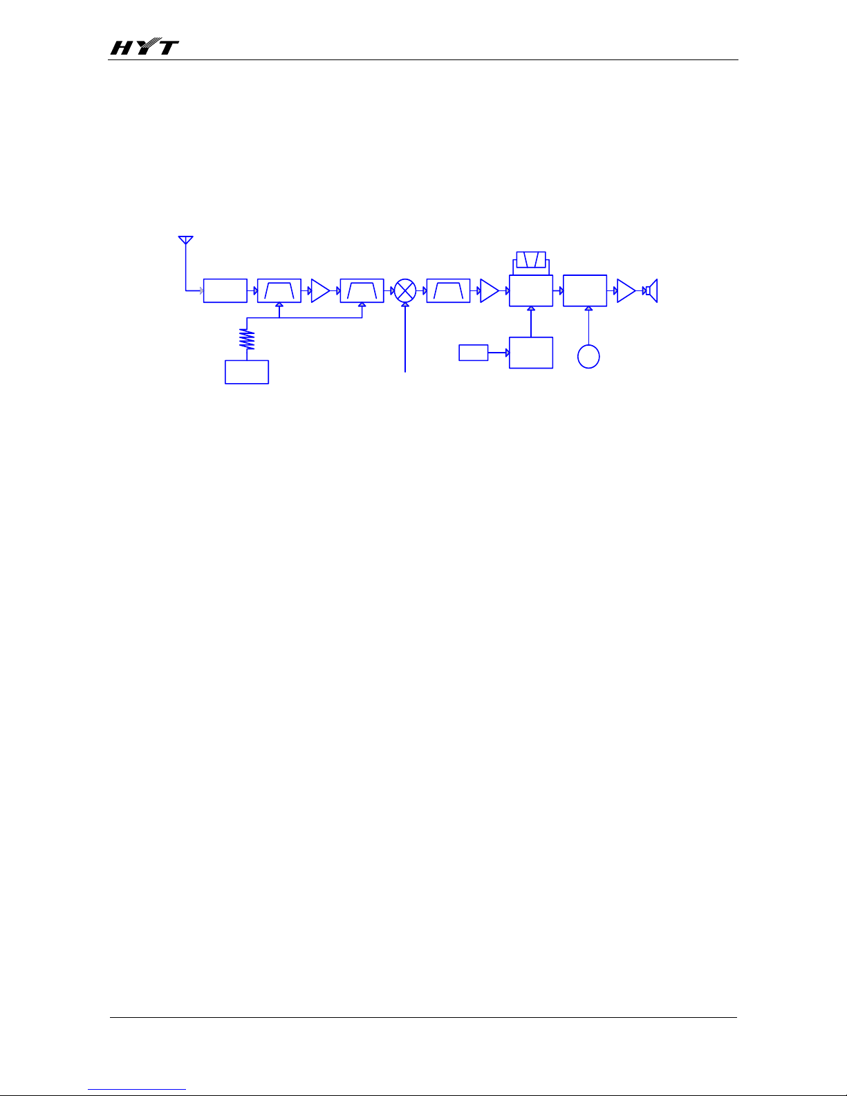
Circuit Description
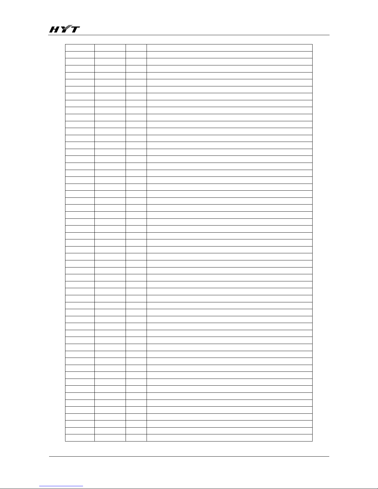
1. Frequency configuration
The receiver utilizes double conversion superheterodyne. The first IF is 38.85MHz and the second IF
is 450kHZ. The first local oscillator signal is supplied from the PLL circuit.
The PLL circuit in the transmitter generates the necessary frequencies. Fig.1 shows the frequencies.
TC-268 frequency range: TC-268(1): 136MHz~150MHz
TC-268(2): 150MHz~174MHz
TC-368 frequency range: TC-368(1): 400MHz~420MHz
TC-368(2): 450MHz~470MHz
B
CC
B
ANT
ANTSW
RF
MCF
38.85MHz
CF
450KHz
SYSTEM
AF
SP
X3
multiply
IF
TCXO 12.8MHz
MIC
AMP
MICPLL
VCO
RX
TX
TX
AMP
PA
AMP
AMP AMP
Fig. 1. Frequency configuration
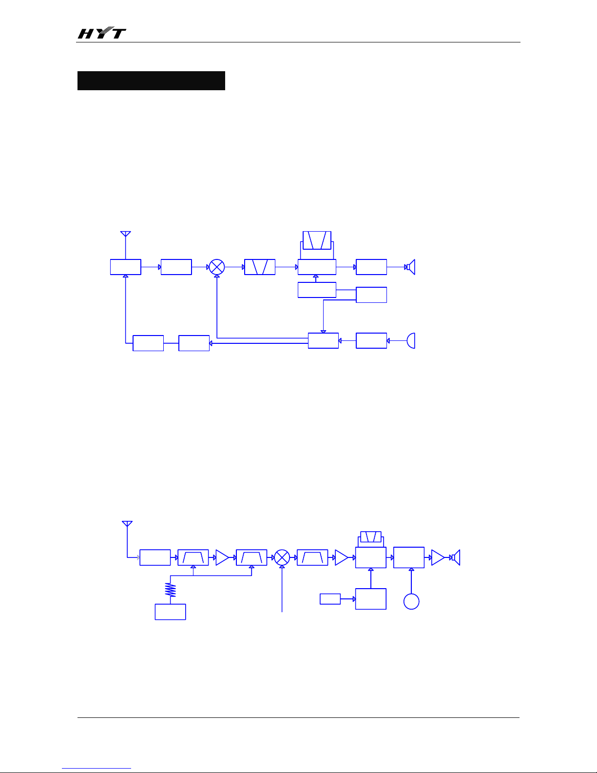
2. Receiver
The receiver employs double conversion superheterodyne.
1-a) Front-end RF amplifier (TC-268)
An input signal from the antenna is applied to an RF amplifier (Q203) after passing through a
transmit/receive switch circuit (D 102 and D103 are off) and a band pass filter (L208, L209 and L210).
After the signal is amplified (Q203), the signal is filtered through a band pass filter (L203 and L214) to
eliminate unwanted signals before it is passed to the first mixer. Band pass filters (L208, L209, L210,
L203 and L214) have varactor diodes (D203, D204, D206, D202 and D201). The voltage of varactor is
provided by the MPU (IC403) center frequency of the band pass filter. (See Fig. 2-a)
B
CC
B
ANT
D102
D103
BPF
Q203
RF AMP
L208-L210
BPF
L214L215
MCF
XF200
IF AMP
Q201
MIXER
Q202
CF200
IF.MIX
IC200
AF AMP
LPF.HPF
IC300
AF PA AMP
IC302
SP
WIDE/NARROW SW
Q303
X3
multiply
Q1
TCXO
1st Local OSC
(PLL)
TUNE
APC
IC403
MCU
Fig. 2-a. Receiver configuration
Page 12
TC-268/368 Service Manual
10
1-b) Front-end RF amplifier (TC-368)
An input signal from the antenna is applied to a RF amplifier (Q203) after passing through a
transmit/receive switch circuit (K102 and D103 are off) and a 3-pole LC filter. After the signal is
amplified (Q203), the signal is filtered by a band pass filter (a 3-pole LC filter) to eliminate unwanted
signals before it is passed to the first mixer. The voltage of varactor is provided by the MPU. (See Fig.
2-b)
B
CC
B
ANT
D102
D103
BPF
Q203
RF AMP
L208-L211
BPF
L214.L203.L204
MCF
XF200
IF AMP
Q201
MIXER
Q202
CF200
IF.MIX
IC200
AF AMP
LPF.HPF
IC300
AF PA AMP
IC302
SP
WIDE/NARROW SW
Q303
X3
multiply
Q1
TCXO
1st Local OSC
(PLL)
TUNE
APC
IC403
MCU
Fig. 2-b. Receiver configuration
2) First mixer
The signal from the RF amplifier is heterodyned with the first local oscillator signal from the PLL
frequency synthesizer circuit at the first mixer (Q202) to create a 38.85 MHz first intermediate frequency
(1
st
IF) signal. The first IF signal is then fed through two monolithic crystal filters (MCFs: XF200) to
further remove spurious signals.
3) IF amplifier
The first IF signal is amplified by Q201, and then enters IC 200 (IF processing IC). The signal is
heterodyned again with a second local oscillator signal within IC200 to create a 450kHz second IF
signal. The second IF signal is then fed through a 450kHz ceramic filter (CF200) to further eliminate
unwanted signals before it is amplified and FM detected in IC200.
4) AF amplifier
The recovered AF signal obtained from IC200 is amplified by IC300 (1/4), filtered by the IC300
low-pass filter (2/4) and IC300 high-pass filter (3/4) and (4/4), and de-emphasized by R303 and C306,
and then passed through a WIDE/NARROW switch (Q303). The processed AF signal passes through
an AF volume control and is amplified by an AF power amplifier (IC302) to a sufficient level to drive a
loud speaker.
5) Squelch
Part of the AF signal from the IC re-enters the FM IC, and the noise component is amplified and
rectified by a filter and an amplifier to produce a DC voltage corresponding to the noise level.
The DC signal from the FM IC goes to the analog port of the microprocessor (IC403). IC403 determines
whether to output sounds from the speaker, IC403 sends a high signal to the MUTE and AFCO lines and turns
IC302 on through Q302, Q304, Q305, Q306 and Q307. (See Fig.3)
Page 13
TC-268/368 Service Manual
11
FM IF IC200
IF AMP DET
DET HPF
AMP
IC 300
AF AMP LPF HPF
Q302SWIC302
AF/PF AMP
Q307
SW
SP
Q304.Q305.Q306
SW
Q303
W/N SW
IC301
LPF
562676
BUSY
MUTE
AFCO
TI
IC403
MPU
Fig. 3. AF Amplifier and squelch
6) Receiving signaling
CTCSS/CDCSS
300 Hz and higher audio frequencies of the output signal from IF IC are cut by a low-pass filter
(IC301). The resulting signal enters the microprocessor (IC403). IC403 determines whether the CTCSS
or CDCSS matches the preset value, and controls the MUTE and AFCO and the speaker output sounds
according to the squelch results.
3. PLL frequency synthesizer
The PLL circuit generates the first local oscillator signal for reception and the RF signal for
transmission.
1) PLL
The frequency step of the PLL circuit is 5 or 6.25kHz. A 12.8MHz reference oscillator signal is divided
at IC1 by a fixed counter to produce the 5 or 6.25kHz reference frequency. The voltage controlled
oscillator (VCO) output signal is buffer amplified by Q6, then divided in IC1 by a dual-module
programmable counter. The divided signal is compared in phase with the 5 or 6.25kHz reference signal
in the phase comparator in IC1. The output signal from the phase comparator is filtered through a
low-pass filter and passed to the VCO to control the oscillator frequency. (See Fig. 4 of Next Page)
B
C
DD
C
B
PLL DATA
PLL IC IC1
I/N
5KHz/6.25KHz
PHASE
COMPARATOR
REF OSC
12.8MHz
I/M
5KHz/6.25KHz
CHARGE
LPF
D2.4Q4TX VCO
D1.3Q3RX VCO
Q6
BUFF AMP
Q5.7
T/R SW
Q2
RF AMP
PUMP
Fig. 4. PLL circuit
Page 14
TC-268/368 Service Manual
12
2) VCO
The operating frequency is generated by Q4 in transmit mode and Q3 in receive mode. The oscillator
frequency is controlled by applying the VCO control voltage, obtained from the phase comparator, to the
varactor diodes (D2 and D4 in transmit mode and D1 and D3 in receive mode). The T/R pin is set high
in receive mode causing Q5 and Q7 to turn Q4 off, and turn Q3 on. The T/R pin is set low in transmit
mode. The outputs from Q3 and Q4 are amplified by Q6 and sent to the buffer amplifiers.
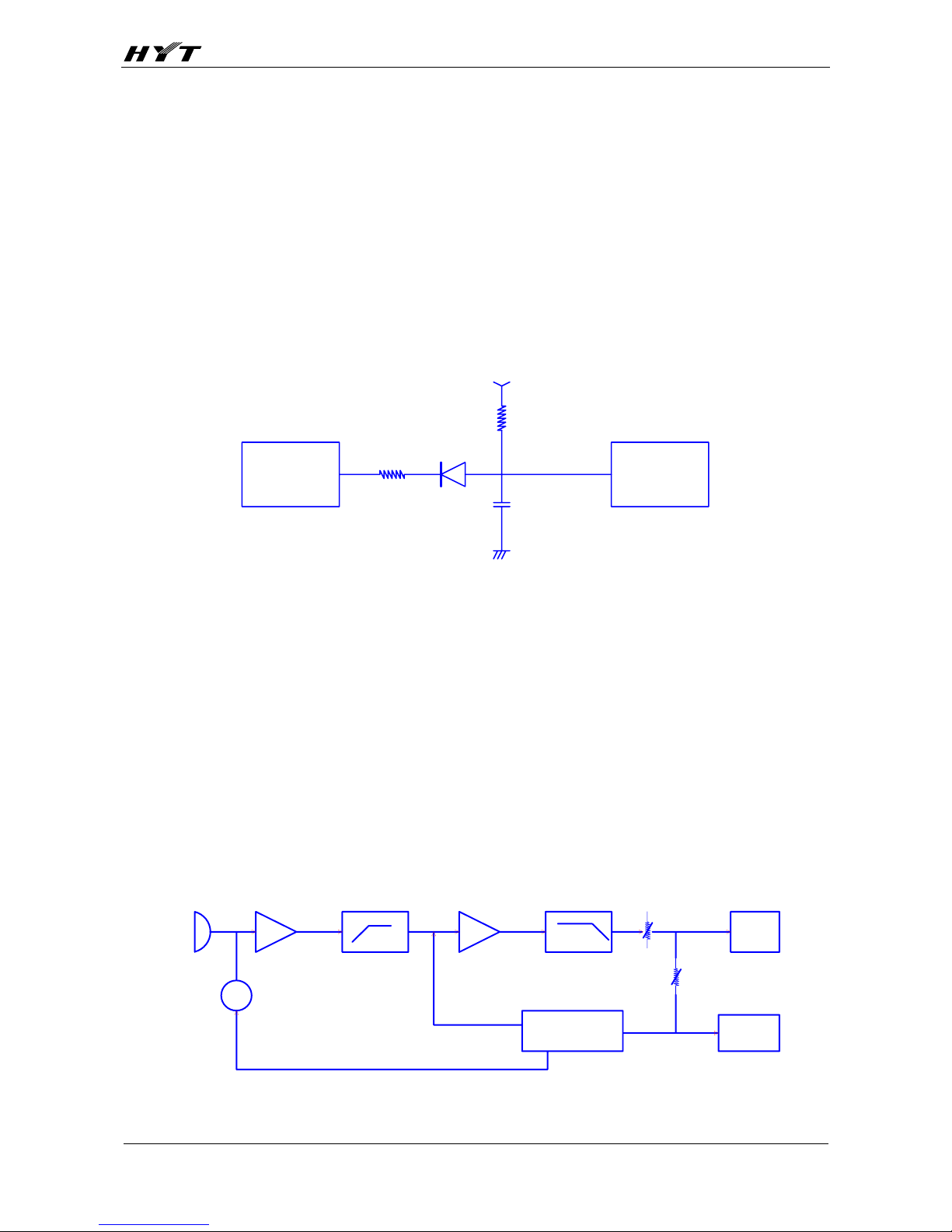
3) UNLOCK DETECTOR
If a pulse signal appears at the LD pin of IC1, an unlock condition occurs, and the DC voltage
obtained from D7, R6, and C1 causes the voltage applied to the UL pin of the microprocessor to go low.
When the microprocessor detects this condition, the transmitter is disabled, ignoring the push-to-talk
switch input signal. (See Fig. 5)
IC1
LD
PLL IC
D7
5C
R6
C1
IC403
UL
MPU
Fig. 5. Unlock detector circuit
4. Transmitter
1) Transmit audio
The modulation signal from the microphone is amplified by IC500 (1/2), passes through a
pre-emphasis circuit, and amplified by the other IC500 (1/2) to perform IDC operation. The signal then
passes through a low-pass filter (splatter filter) (Q501 and Q502) and cuts 3kHz and higher frequencies.
The resulting signal goes to the VCO through the VCO modulation terminal
for direct FM modulation. (See Fig. 6)
2) CTCSS/CDCSS encoder
A necessary signal for CTCSS/CDCSS encoding is generated by IC403 and FM-modulated to the
PLL reference signal. Since the reference OSC does not modulate the loop characteristic frequency or
higher, modulation is performed at the VCO side by adjusting the balance. (See Fig. 6)
VCO
D5.Q4
VR500
BALANCE
VR501
MAX
DEV
X1.IC1
PEFERENCE
OSC
CTCSS/CDCSS
TO
TTS
TTS
MUTE
Q503
SW
MIC
IC500(1/2)
MIC
AMP
PREEMPHASIS
IC500(1/2)
IDC
Q501.502
LPF
(SPATTER FILTER)
IC403
Fig. 6. Transmit audio CTCSS/CDCSS
Page 15
TC-268/368 Service Manual
13
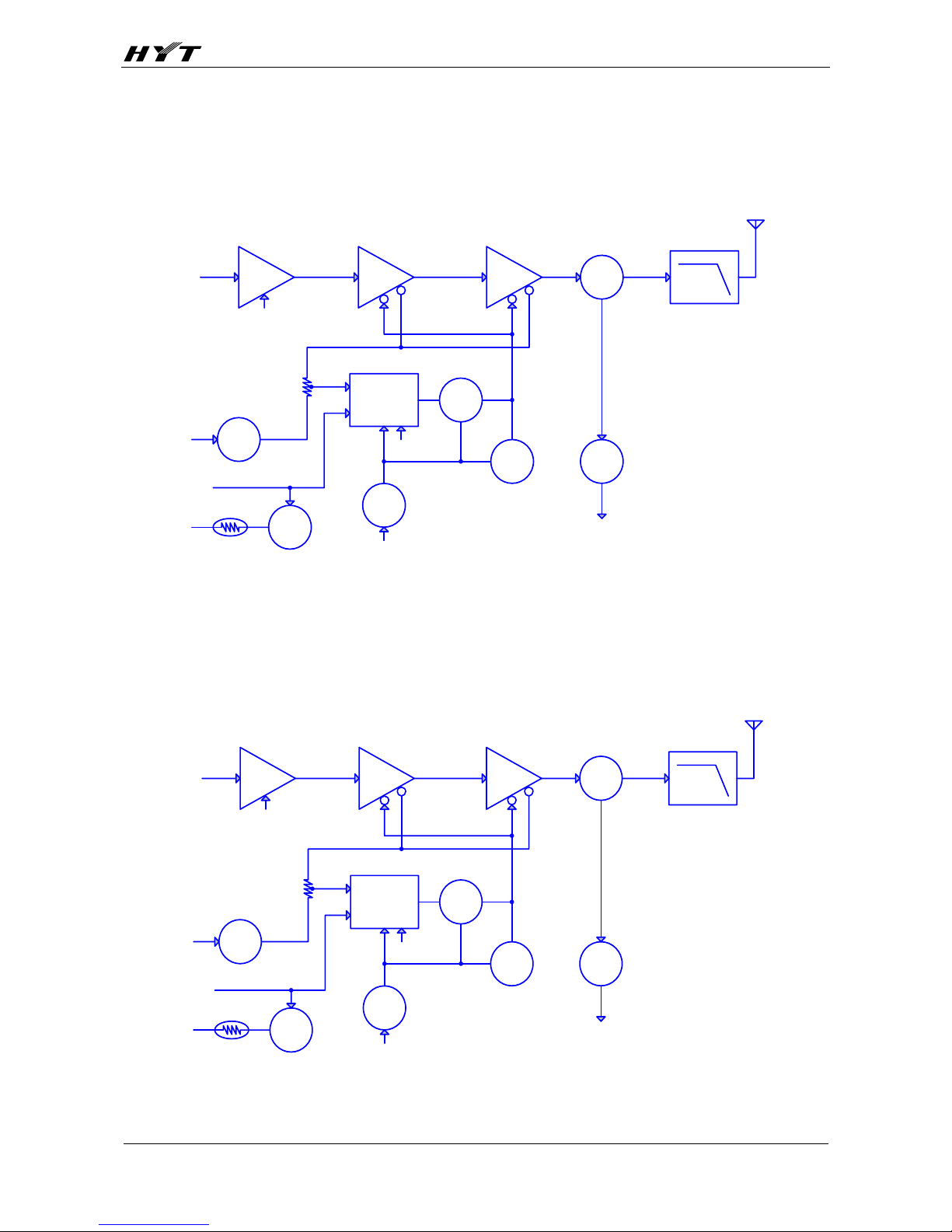
3-a) RF amplifier (TC-268)
The transmit signal obtained from the VCO buffer amplifier Q100, is amplified by Q101. This amplified
signal is passed to the power amplifier, Q102 and Q105, which consists of a 2-stage FET amplifier and
is capable of producing up to 5W of RF power (See Fig. 7-a)
D
C
B
A
Title
Number RevisionSize
AMP
Q101
5T
DRIVE AMP
Q102
FINAL AMP
Q105
ANT SW
D101 LPF
ANT
ANT SW
D102.103
RX
Q106
SW
Q109
SW
5T
IC100
APC
DET
Q103.Q104
B SW
B
APC
5T
TH100
SW
Q107
5T
Q108
SW
Fig. 7-a. APC system
3-b) RF amplifier (TC-368)
The transmit signal obtained from the VCO buffer amplifier Q100, is amplified by Q101 and Q102.
This amplified signal is passed to the power amplifier, Q105 and Q107, which consists of
a 2-stage FET amplifier and is capable of producing up to 4W of RF power (See Fig. 7-b)
D
C
B
A
Title
Number RevisionSize
AMP
Q101.102
5T
DRIVE AMP
Q105
FINAL AMP
Q107
ANT SW
D101 LPF
ANT
ANT SW
D102.103
RX
Q106
SW
Q109
SW
5T
IC100
APC
DET
Q103.Q104
B SW
B
APC
5T
TH102
SW
Q110
5T
Q108
SW
Fig. 7-b. APC system
Page 16

TC-268/368 Service Manual
14
4) ANT switch and LPF
The RF amplifier output signal is passed through a low-pass filter network and a transmit/receive
switching circuit before it is passed to the antenna terminal. The transmit/receive switching circuit is
comprised of D101, D102 and D103. D102 and D103 turned on (conductive) in transmit mode and off
(isolated) in receive mode.
5) APC
The automatic power control (APC) circuit stabilizes the transmitter output power at a predetermined
level by sensing the drain current of the final amplifier Field Effect Transistor (FET). The voltage
obtained from the above drain current with a reference voltage which is set using the microprocessor.
An APC voltage proportional to the difference between the sensed voltage and the reference voltage
appears at the output of IC100 (1/2). This output voltage controls the gate of the FET power amplifier,
which keeps the transmitter output power can be varied by the microprocessor which in turn changes
the reference voltage and hence , the output power.
6) Terminal protection circuit
When the thermistor (TH102) reaches about 80 , the protection circuit turns on Q110 to protect ℃
transmitting final amplifier (Q107).
5. Power supply
A 5V reference power supply [5M] for the control circuit is derived from an internal battery. This
reference is used to provide a 5V supply in transmit mode [5T], a 5V supply in receive mode [5R] , and
a 5V, supply common in both modes [5C] based on the control signal sent from the microprocessor.
6. Control system
The IC403 CPU operates at 7.37MHZ. This oscillator has a circuit that shifts the frequency according
to the EEPROM data.
Page 17

TC-268/368 Service Manual
15
Parts List 1
No. Material No. Material Name Qty Ref No. Print No.
1 3001060000000 Chip resistor 0603 0Ω J 1/10W 1 R118 B3G
2 3001060000000 Chip resistor 0603 0Ω J 1/10W 1 R123 B4I
3 3001060000000 Chip resistor 0603 0Ω J 1/10W 1 R213 B5E
4 3001060000000 Chip resistor 0603 0Ω J 1/10W 1 R222 B4E
5 3001060000000 Chip resistor 0603 0Ω J 1/10W 1 R232 B5F
6 3001060000000 Chip resistor 0603 0Ω J 1/10W 1 R233 B4F
7 3001060000000 Chip resistor 0603 0Ω J 1/10W 1 R240 B4H
8 3001060000000 Chip resistor 0603 0Ω J 1/10W 1 R28 B1D
9 3001060000000 Chip resistor 0603 0Ω J 1/10W 1 R29 B2C
10 3001060000000 Chip resistor 0603 0Ω J 1/10W 1 R327 T2E
11 3001060000000 Chip resistor 0603 0Ω J 1/10W 1 R329 B2A
12 3001060000000 Chip resistor 0603 0Ω J 1/10W 1 R404 T2B
13 3001060000000 Chip resistor 0603 0Ω J 1/10W 1 R419 B2I
14 3001060000000 Chip resistor 0603 0Ω J 1/10W 1 R431 T4J
15 3001060000000 Chip resistor 0603 0Ω J 1/10W 1 R5 B1C
16 3001060000000 Chip resistor 0603 0Ω J 1/10W 1 R531 T2G
17 3001060000000 Chip resistor 0603 0Ω J 1/10W 1 R539 T5H
18 3001060000000 Chip resistor 0603 0Ω J 1/10W 1 R542 T3G
19 3001060000000 Chip resistor 0603 0Ω J 1/10W 1 R7 B1C
20 3001061000000 Chip resistor 0603 10Ω J 1/10 1 R109 B3G
21 3001061000000 Chip resistor 0603 10Ω J 1/10 1 R200 B5C
22 3001061000000 Chip resistor 0603 10Ω J 1/10 1 R3 B2D
23 3001061000000 Chip resistor 0603 10Ω J 1/10 1 R334 T2F
24 3001061000000 Chip resistor 0603 10Ω J 1/10 1 R412 T3B
25 3001061000000 Chip resistor 0603 10Ω J 1/10 1 R417 T4K
26 3001061010000 Chip resistor 0603 100Ω J 1/1 1 R104 B2G
27 3001061010000 Chip resistor 0603 100Ω J 1/1 1 R14 B3D
28 3001061010000 Chip resistor 0603 100Ω J 1/1 1 R223 B3E
29 3001061010000 Chip resistor 0603 100Ω J 1/1 1 R430 T4J
30 3001061010000 Chip resistor 0603 100Ω J 1/1 1 R530 T4H
31 3001061010000 Chip resistor 0603 100Ω J 1/1 1 R537 T5I
32 3001061010000 Chip resistor 0603 100Ω J 1/1 1 R538 T5H
33 3001061020010 Chip resistor 0603 1KΩ J 1/10 1 R103 B2F
34 3001061020010 Chip resistor 0603 1K
Ω J 1/10 1 R2 B1C
35 3001061020010 Chip resistor 0603 1KΩ J 1/10 1 R20 B2D
36 3001061020010 Chip resistor 0603 1KΩ J 1/10 1 R225 B3E
37 3001061020010 Chip resistor 0603 1KΩ J 1/10 1 R229 B5E
38 3001061020010 Chip resistor 0603 1KΩ J 1/10 1 R27 B1F
39 3001061020010 Chip resistor 0603 1KΩ J 1/10 1 R328 B1A
40 3001061020010 Chip resistor 0603 1KΩ J 1/10 1 R4 B3D
41 3001061020010 Chip resistor 0603 1KΩ J 1/10 1 R405 T4B
42 3001061020010 Chip resistor 0603 1KΩ J 1/10 1 R407 T2A
43 3001061020010 Chip resistor 0603 1KΩ J 1/10 1 R409 T3B
44 3001061020010 Chip resistor 0603 1KΩ J 1/10 1 R413 T2D
45 3001061020010 Chip resistor 0603 1KΩ J 1/10 1 R420 B2I
46 3001061020010 Chip resistor 0603 1KΩ J 1/10 1 R427 B2H
TC-268 (1) Parts List 1
Page 18

TC-268/368 Service Manual
16
Parts List 1
47 3001061020010 Chip resistor 0603 1KΩ J 1/10 1 R508 T3E
48 3001061020010 Chip resistor 0603 1KΩ J 1/10 1 R536 T5J
49 3001061020010 Chip resistor 0603 1KΩ J 1/10 1 R6 T5C
50 3001061020010 Chip resistor 0603 1KΩ J 1/10 1 R608 T1A
51 3001061020010 Chip resistor 0603 1KΩ J 1/10 1 R703 T4I
52 3001061030010 Chip resistor 0603 10KΩ J 1/1 1 R140 T2I
53 3001061030010 Chip resistor 0603 10KΩ J 1/1 1 R15 B1D
54 3001061030010 Chip resistor 0603 10KΩ J 1/1 1 R214 B3E
55 3001061030010 Chip resistor 0603 10KΩ J 1/1 1 R308 B3A
56 3001061030010 Chip resistor 0603 10KΩ J 1/1 1 R432 B2H
57 3001061030010 Chip resistor 0603 10KΩ J 1/1 1 R435 B2H
58 3001061030010 Chip resistor 0603 10KΩ J 1/1 1 R511 T3F
59 3001061030010 Chip resistor 0603 10KΩ J 1/1 1 R516 T3F
60 3001061030010 Chip resistor 0603 10KΩ J 1/1 1 R601 T2A
61 3001061030010 Chip resistor 0603 10KΩ J 1/1 1 R603 T2A
62 3001061030010 Chip resistor 0603 10KΩ J 1/1 1 R605 T2A
63 3001061030010 Chip resistor 0603 10KΩ J 1/1 1 R701 T4H
64 3001061030010 Chip resistor 0603 10KΩ J 1/1 1 R702 T4H
65 3001061040010 Chip resistor 0603 100KΩ J 1/ 1 R146 T1H
66 3001061040010 Chip resistor 0603 100KΩ J 1/ 1 R17 B2E
67 3001061040010 Chip resistor 0603 100KΩ J 1/ 1 R207 B5B
68 3001061040010 Chip resistor 0603 100KΩ J 1/ 1 R21 B2D
69 3001061040010 Chip resistor 0603 100KΩ J 1/ 1 R226 B4E
70 3001061040010 Chip resistor 0603 100KΩ J 1/ 1 R230 B5F
71 3001061040010 Chip resistor 0603 100KΩ J 1/ 1 R237 B4F
72 3001061040010 Chip resistor 0603 100KΩ J 1/ 1 R238 B4H
73 3001061040010 Chip resistor 0603 100KΩ J 1/ 1 R239 B4H
74 3001061040010 Chip resistor 0603 100KΩ J 1/ 1 R24 B1F
75 3001061040010 Chip resistor 0603 100KΩ J 1/ 1 R291 B4F
76 3001061040010 Chip resistor 0603 100KΩ J 1/ 1 R294 B4F
77 3001061040010 Chip resistor 0603 100KΩ J 1/ 1 R323 B4A
78 3001061040010 Chip resistor 0603 100KΩ J 1/ 1 R325 B4A
79 3001061040010 Chip resistor 0603 100KΩ J 1/ 1 R341 T1F
80 3001061040010 Chip resistor 0603 100KΩ
J 1/ 1 R401 T4C
81 3001061040010 Chip resistor 0603 100KΩ J 1/ 1 R408 T2A
82 3001061040010 Chip resistor 0603 100KΩ J 1/ 1 R533 T4I
83 3001061050010 Chip resistor 0603 1MΩ J 1/10 1 R142 T2I
84 3001061050010 Chip resistor 0603 1MΩ J 1/10 1 R304 B3B
85 3001061230000 Chip resistor 0603 12KΩ J 1/1 1 R101 B2F
86 3001061230000 Chip resistor 0603 12KΩ J 1/1 1 R312 B2B
87 3001061240000 Chip resistor 0603 120KΩ D 1/ 1 R23 B2F
88 3001061240000 Chip resistor 0603 120KΩ D 1/ 1 R306 B3A
89 3001061240000 Chip resistor 0603 120KΩ D 1/ 1 R340 B1B
90 3001061240000 Chip resistor 0603 120KΩ D 1/ 1 R509 T2C
91 3001061510000 Chip resistor 0603 150Ω J 1/1 1 R10 B1D
92 3001061510000 Chip resistor 0603 150Ω J 1/1 1 R13 B1D
93 3001061510000 Chip resistor 0603 150Ω J 1/1 1 R231 B5F
94 3001061510000 Chip resistor 0603 150Ω J 1/1 1 R332 T2E
TC-268 (1) Parts List 1
Page 19

TC-268/368 Service Manual
17
Parts List 1
95 3001061520000 Chip resistor 0603 1.5KΩ J 1/ 1 R108 B3F
96 3001061520000 Chip resistor 0603 1.5KΩ J 1/ 1 R525 T4G
97 3001061530000 Chip resistor 0603 15KΩ D 1/1 1 R433 B2H
98 3001061530000 Chip resistor 0603 15KΩ D 1/1 1 R434 B1H
99 3001061530000 Chip resistor 0603 15KΩ D 1/1 1 R513 T2C
100 3001061530000 Chip resistor 0603 15KΩ D 1/1 1 R526 T3G
101 3001061530000 Chip resistor 0603 15KΩ D 1/1 1 R527 T3G
102 3001061530010 Chip resistor 0603 15KΩ J 1/1 1 R143 T1H
103 3001061540010 Chip resistor 0603 150KΩ D 1/ 1 R1 B1C
104 3001061540010 Chip resistor 0603 150KΩ D 1/ 1 R133 T1I
105 3001061540010 Chip resistor 0603 150KΩ D 1/ 1 R134 T1I
106 3001061540010 Chip resistor 0603 150KΩ D 1/ 1 R135 T1I
107 3001061540010 Chip resistor 0603 150KΩ D 1/ 1 R136 T1I
108 3001061540010 Chip resistor 0603 150KΩ D 1/ 1 R137 T1I
109 3001061540010 Chip resistor 0603 150KΩ D 1/ 1 R138 T1I
110 3001061540010 Chip resistor 0603 150KΩ D 1/ 1 R518 T2C
111 3001061800000 Chip resistor 0603 18Ω J 1/10 1 R112 B3F
112 3001061810000 Chip resistor 0603 180Ω J 1/1 1 R403 B2K
113 3001061820000 Chip resistor 0603 1.8KΩ J 1/ 1 R114 B3G
114 3001061820000 Chip resistor 0603 1.8KΩ J 1/ 1 R522 T3F
115 3001061820000 Chip resistor 0603 1.8KΩ J 1/ 1 R534 T5H
116 3001061830010 Chip resistor 0603 18KΩ J 1/1 1 R305 B2A
117 3001061830010 Chip resistor 0603 18KΩ J 1/1 1 R529 T4G
118 3001061840000 Chip resistor 0603 180KΩ J 1/ 1 R145 T1I
119 3001061840000 Chip resistor 0603 180KΩ J 1/ 1 R202 B4B
120 3001061840000 Chip resistor 0603 180KΩ J 1/ 1 R206 B4B
121 3001061840000 Chip resistor 0603 180KΩ J 1/ 1 R293 B4F
122 3001061840000 Chip resistor 0603 180KΩ J 1/ 1 R318 B4A
123 3001061850000 Chip resistor 0603 1.8MΩ J 1/ 1 R512 T3E
124 3001061850000 Chip resistor 0603 1.8MΩ J 1/ 1 R517 T3F
125 3001062210000 Chip resistor 0603 220Ω J 1/1 1 R102 B2F
126 3001062210000 Chip resistor 0603 220Ω J 1/1 1 R210 B5C
127 3001062210000 Chip resistor 0603 220Ω J 1/1 1 R402 B2K
128 3001062220000 Chip resistor 0603 2.2KΩ
J 1/ 1 R331 T1E
129 3001062220000 Chip resistor 0603 2.2KΩ J 1/ 1 R406 B2J
130 3001062220000 Chip resistor 0603 2.2KΩ J 1/ 1 R418 T2C
131 3001062230000 Chip resistor 0603 22KΩ J 1/1 1 R321 B1B
132 3001062230000 Chip resistor 0603 22KΩ J 1/1 1 R504 T2D
133 3001062240000 Chip resistor 0603 220KΩ D 1/ 1 R322 B2A
134 3001062240000 Chip resistor 0603 220KΩ D 1/ 1 R411 T2A
135 3001062710000 Chip resistor 0603 270Ω J 1/1 1 R127 B4J
136 3001062710000 Chip resistor 0603 270Ω J 1/1 1 R128 B4J
137 3001062710000 Chip resistor 0603 270Ω J 1/1 1 R18 B1F
138 3001062710000 Chip resistor 0603 270Ω J 1/1 1 R22 B1E
139 3001062720000 Chip resistor 0603 2.7KΩ J 1/ 1 R209 B5C
140 3001062720000 Chip resistor 0603 2.7KΩ J 1/ 1 R422 B2H
141 3001062720000 Chip resistor 0603 2.7KΩ J 1/ 1 R428 B2H
142 3001062740000 Chip resistor 0603 270KΩ D 1/ 1 R316 B3A
TC-268 (1) Parts List 1
Page 20

TC-268/368 Service Manual
18
Parts List 1
143 3001062740000 Chip resistor 0603 270KΩ D 1/ 1 R317 B2B
144 3001063300000 Chip resistor 0603 33Ω J 1/10 1 R212 B3E
145 3001063310010 Chip resistor 0603 330Ω J 1/1 1 R110 B3F
146 3001063310010 Chip resistor 0603 330Ω J 1/1 1 R144 T2H
147 3001063310010 Chip resistor 0603 330Ω J 1/1 1 R147 B3F
148 3001063310010 Chip resistor 0603 330Ω J 1/1 1 R148 B3G
149 3001063310010 Chip resistor 0603 330Ω J 1/1 1 R30 B2B
150 3001063320000 Chip resistor 0603 3.3KΩ J 1/ 1 R100 B2F
151 3001063320000 Chip resistor 0603 3.3KΩ J 1/ 1 R105 B3F
152 3001063320000 Chip resistor 0603 3.3KΩ J 1/ 1 R106 B3F
153 3001063320000 Chip resistor 0603 3.3KΩ J 1/ 1 R120 B3G
154 3001063320000 Chip resistor 0603 3.3KΩ J 1/ 1 R125 T2H
155 3001063320000 Chip resistor 0603 3.3KΩ J 1/ 1 R203 B4B
156 3001063320000 Chip resistor 0603 3.3KΩ J 1/ 1 R204 B4B
157 3001063320000 Chip resistor 0603 3.3KΩ J 1/ 1 R303 B2B
158 3001063320000 Chip resistor 0603 3.3KΩ J 1/ 1 R424 B2I
159 3001063320000 Chip resistor 0603 3.3KΩ J 1/ 1 R425 B2I
160 3001063320000 Chip resistor 0603 3.3KΩ J 1/ 1 R510 T3E
161 3001063320000 Chip resistor 0603 3.3KΩ J 1/ 1 R521 T3F
162 3001063320000 Chip resistor 0603 3.3KΩ J 1/ 1 R548 T2D
163 3001063330010 Chip resistor 0603 33KΩ J 1/1 1 R336 T2F
164 3001063330010 Chip resistor 0603 33KΩ J 1/1 1 R514 T3E
165 3001063330010 Chip resistor 0603 33KΩ J 1/1 1 R515 T3F
166 3001063330010 Chip resistor 0603 33KΩ J 1/1 1 R519 T3F
167 3001063330010 Chip resistor 0603 33KΩ J 1/1 1 R520 T3F
168 3001063340000 Chip resistor 0603 330KΩ J 1/ 1 R400 T2B
169 3001063340000 Chip resistor 0603 330KΩ J 1/ 1 R8 B3D
170 3001063920000 Chip resistor 0603 3.9KΩ J 1/ 1 R107 B3F
171 3001063920000 Chip resistor 0603 3.9KΩ J 1/ 1 R201 B3B
172 3001063920000 Chip resistor 0603 3.9KΩ J 1/ 1 R220 B3E
173 3001063930010 Chip resistor 0603 39KΩ J 1/1 1 R12 B3B
174 3001063930010 Chip resistor 0603 39KΩ J 1/1 1 R607 T2B
175 3001063940000 Chip resistor 0603 390KΩ D 1/ 1 R315 B1A
176 3001064700000 Chip resistor 0603 47Ω
J 1/10 1 R116 B3G
177 3001064700000 Chip resistor 0603 47Ω J 1/10 1 R117 B3H
178 3001064700000 Chip resistor 0603 47Ω J 1/10 1 R215 B3E
179 3001064700000 Chip resistor 0603 47Ω J 1/10 1 R228 B5E
180 3001064710000 Chip resistor 0603 470Ω J 1/1 1 R211 B3E
181 3001064710000 Chip resistor 0603 470Ω J 1/1 1 R535 T5H
182 3001064720000 Chip resistor 0603 4.7KΩ J 1/ 1 R119 T2J
183 3001064720000 Chip resistor 0603 4.7KΩ J 1/ 1 R26 B2G
184 3001064720000 Chip resistor 0603 4.7KΩ J 1/ 1 R416 T4C
185 3001064720000 Chip resistor 0603 4.7KΩ J 1/ 1 R500 T2C
186 3001064720000 Chip resistor 0603 4.7KΩ J 1/ 1 R501 T2C
187 3001064720000 Chip resistor 0603 4.7KΩ J 1/ 1 R507 T4C
188 3001064720000 Chip resistor 0603 4.7KΩ J 1/ 1 R541 T5C
189 3001064730000 Chip resistor 0603 47KΩ J 1/1 1 R11 B3B
190 3001064730000 Chip resistor 0603 47KΩ J 1/1 1 R115 B3G
TC-268 (1) Parts List 1
Page 21
TC-268/368 Service Manual
19
Parts List 1
191 3001064730000 Chip resistor 0603 47KΩ J 1/1 1 R121 B3G
192 3001064730000 Chip resistor 0603 47KΩ J 1/1 1 R141 T1I
193 3001064730000 Chip resistor 0603 47KΩ J 1/1 1 R19 B2E
194 3001064730000 Chip resistor 0603 47KΩ J 1/1 1 R307 B2A
195 3001064730000 Chip resistor 0603 47KΩ J 1/1 1 R320 B3B
196 3001064730000 Chip resistor 0603 47KΩ J 1/1 1 R330 T2D
197 3001064730000 Chip resistor 0603 47KΩ J 1/1 1 R338 B2A
198 3001064730000 Chip resistor 0603 47KΩ J 1/1 1 R414 T4K
199 3001064730000 Chip resistor 0603 47KΩ J 1/1 1 R415 T4K
200 3001064730000 Chip resistor 0603 47KΩ J 1/1 1 R421 T4J
201 3001064730000 Chip resistor 0603 47KΩ J 1/1 1 R423 T4J
202 3001064730000 Chip resistor 0603 47KΩ J 1/1 1 R600 T1A
203 3001064730000 Chip resistor 0603 47KΩ J 1/1 1 R606 T2B
204 3001064740000 Chip resistor 0603 470KΩ D 1/ 1 R309 B3B
205 3001064740000 Chip resistor 0603 470KΩ D 1/ 1 R314 B1B
206 3001064740000 Chip resistor 0603 470KΩ D 1/ 1 R333 T1F
207 3001065130010 Chip resistor 0603 51KΩ J 1/1 1 R524 T3F
208 3001065610000 Chip resistor 0603 560Ω J 1/1 1 R124 T2H
209 3001065620000 Chip resistor 0603 5.6KΩ D 1/ 1 R301 B3B
210 3001065620000 Chip resistor 0603 5.6KΩ D 1/ 1 R302 B3B
211 3001065620000 Chip resistor 0603 5.6KΩ D 1/ 1 R324 B1B
212 3001065620000 Chip resistor 0603 5.6KΩ D 1/ 1 R326 B1A
213 3001065620000 Chip resistor 0603 5.6KΩ D 1/ 1 R604 T2A
214 3001065630000 Chip resistor 0603 56KΩ J 1/1 1 R335 T2F
215 3001066810010 Chip resistor 0603 680Ω J 1/1 1 R122 T2J
216 3001066810010 Chip resistor 0603 680Ω J 1/1 1 R126 T2J
217 3001066810010 Chip resistor 0603 680Ω J 1/1 1 R25 B2F
218 3001066810010 Chip resistor 0603 680Ω J 1/1 1 R9 B1C
219 3001066820000 Chip resistor 0603 6.8KΩ J 1/ 1 R503 T2D
220 3001066820000 Chip resistor 0603 6.8KΩ J 1/ 1 R505 T2D
221 3001066820000 Chip resistor 0603 6.8KΩ J 1/ 1 R523 T3F
222 3001066830000 Chip resistor 0603 68KΩ J 1/1 1 R16 B2E
223 3001066840000 Chip resistor 0603 680KΩ J 1/ 1 R208 B5C
224 3001066840000 Chip resistor 0603 680KΩ
J 1/ 1 R602 T1A
225 3001067540000 Chip resistor 0603 750KΩ J 1/ 1 R528 T4G
226 3001068210010 Chip resistor 0603 820Ω J 1/1 1 R205 B5B
227 3001068210010 Chip resistor 0603 820Ω J 1/1 1 R429 B2H
228 3001068210010 Chip resistor 0603 820Ω J 1/1 1 R506 T3E
229 3001068210010 Chip resistor 0603 820Ω J 1/1 1 R532 T4H
230 3001068220000 Chip resistor 0603 8.2KΩ J 1/ 1 R339 T1D
231 3001068220000 Chip resistor 0603 8.2KΩ J 1/ 1 R410 B2K
232 3001068220000 Chip resistor 0603 8.2KΩ J 1/ 1 R426 B2K
233 3001068230010 Chip resistor 0603 82KΩ J 1/1 1 R295 B3E
234 3001068230010 Chip resistor 0603 82KΩ J 1/1 1 R296 B3E
235 3001068230010 Chip resistor 0603 82KΩ J 1/1 1 R297 B3E
236 3001068230010 Chip resistor 0603 82KΩ J 1/1 1 R298 B3E
237 3001068230010 Chip resistor 0603 82KΩ J 1/1 1 R313 B3A
238 3001068230010 Chip resistor 0603 82KΩ J 1/1 1 R502 T5C
TC-268 (1) Parts List 1
Page 22

TC-268/368 Service Manual
20
Parts List 1
239 3001069130000 Chip resistor 0603 91KΩ D 1/1 1 R300 B1B
240 3001070000000 Chip resistor 0805 0Ω J 1/8W 1 R310 T2F
241 3001070000000 Chip resistor 0805 0Ω J 1/8W 1 R311 B3A
242 3001070000000 Chip resistor 0805 0Ω J 1/8W 1 R540 T5B
243 3001080590000 Chip resistor 1206 0.5Ω J 1/4 1 R130 T2J
244 3001080590000 Chip resistor 1206 0.5Ω J 1/4 1 R131 T2J
245 3001080590000 Chip resistor 1206 0.5Ω J 1/4 1 R132 T2J
246 3002991530009 Trimmer resistor 2.7*2.0*1.6 15K 1 VR501 T3E
247 3002996830009 Trimmer resistor 68KΩ 1VR1T2C
248 3002996830009 Trimmer resistor 68KΩ 1 VR500 T2D
249 3003992220000 Thermistor 0603 2.2KΩ J 10 1 TH500 T2C
250 3003994730000 Thermistor 0603 47KΩ J 100 1 TH100 B3H
251 3005991020019 Resistor array 3.2*1.6*1.5) 1KΩ 1 CP1 B1C
252 3101060200010 Chip capacitor 0603 2PF B 50V 1 C216 B4D
253 3101060200010 Chip capacitor 0603 2PF B 50V 1 C243 B4E
254 3101060200010 Chip capacitor 0603 2PF B 50V 1 C254 B4G
255 3101060200010 Chip capacitor 0603 2PF B 50V 1 C257 B4H
256 3101060300010 Chip capacitor 0603 3PF B 50V 1 C409 T3B
257 3101060500010 Chip capacitor 0603 5PF B 50V 1 C258 B4H
258 3101060500010 Chip capacitor 0603 5PF B 50V 1 C37 B2F
259 3101060590010 Chip capacitor 0603 0.5PF B 50 1 C43 B2F
260 3101060590010 Chip capacitor 0603 0.5PF B 50 1 C44 B2F
261 3101060600010 Chip capacitor 0603 6PF B 50V 1 C233 B3E
262 3101060600010 Chip capacitor 0603 6PF B 50V 1 C237 B4E
263 3101060800010 Chip capacitor 0603 8PF B 50V 1 C128 B4I
264 3101060800010 Chip capacitor 0603 8PF B 50V 1 C129 B4I
265 3101060800010 Chip capacitor 0603 8PF B 50V 1 C222 B3E
266 3101060800010 Chip capacitor 0603 8PF B 50V 1 C241 B5G
267 3101060800010 Chip capacitor 0603 8PF B 50V 1 C35 B1F
268 3101060900010 Chip capacitor 0603 9PF B 50V 1 C223 B5D
269 3101060900010 Chip capacitor 0603 9PF B 50V 1 C261 B4H
270 3101061000000 Chip capacitor 0603 10PF J 50V 1 C14 B2D
271 3101061000000 Chip capacitor 0603 10PF J 50V 1 C202 B4B
272 3101061000000 Chip capacitor 0603 10PF J 50V 1 C215 B4D
273 3101061000000 Chip capacitor 0603 10PF J 50V 1 C412 T3B
274 3101061000000 Chip capacitor 0603 10PF J 50V 1 C415 T3B
275 3101061000000 Chip capacitor 0603 10PF J 50V 1 C48 B2D
276 3101061000000 Chip capacitor 0603 10PF J 50V 1 C516 T3F
277 3101061000000 Chip capacitor 0603 10PF J 50V 1 C9 B2D
278 3101061000020 Chip capacitor 0603 10PF B 50V 1 C148 B4G
279 3101061000020 Chip capacitor 0603 10PF B 50V 1 C248 B5E
280 3101061010010 Chip capacitor 0603 100PF J 50 1 C134 T1I
281 3101061010010 Chip capacitor 0603 100PF J 50 1 C2 B1B
282 3101061010010 Chip capacitor 0603 100PF J 50 1 C3 B2B
283 3101061010010 Chip capacitor 0603 100PF J 50 1 C32 B2E
284 3101061010010 Chip capacitor 0603 100PF J 50 1 C6 B1C
285 3101061010010 Chip capacitor 0603 100PF J 50 1 C605 T1A
286 3101061020000 Chip capacitor 0603 1000PF K 5 1 C101 B2F
TC-268 (1) Parts List 1
Page 23

TC-268/368 Service Manual
21
Parts List 1
287 3101061020000 Chip capacitor 0603 1000PF K 5 1 C102 B2F
288 3101061020000 Chip capacitor 0603 1000PF K 5 1 C104 B3F
289 3101061020000 Chip capacitor 0603 1000PF K 5 1 C105 B3F
290 3101061020000 Chip capacitor 0603 1000PF K 5 1 C106 B3G
291 3101061020000 Chip capacitor 0603 1000PF K 5 1 C107 B3G
292 3101061020000 Chip capacitor 0603 1000PF K 5 1 C109 B3G
293 3101061020000 Chip capacitor 0603 1000PF K 5 1 C111 B3G
294 3101061020000 Chip capacitor 0603 1000PF K 5 1 C112 T2J
295 3101061020000 Chip capacitor 0603 1000PF K 5 1 C114 B3G
296 3101061020000 Chip capacitor 0603 1000PF K 5 1 C115 T3J
297 3101061020000 Chip capacitor 0603 1000PF K 5 1 C116 B3G
298 3101061020000 Chip capacitor 0603 1000PF K 5 1 C118 B3G
299 3101061020000 Chip capacitor 0603 1000PF K 5 1 C119 B3H
300 3101061020000 Chip capacitor 0603 1000PF K 5 1 C120 B3I
301 3101061020000 Chip capacitor 0603 1000PF K 5 1 C124 B3I
302 3101061020000 Chip capacitor 0603 1000PF K 5 1 C130 T2H
303 3101061020000 Chip capacitor 0603 1000PF K 5 1 C133 B4J
304 3101061020000 Chip capacitor 0603 1000PF K 5 1 C137 B4I
305 3101061020000 Chip capacitor 0603 1000PF K 5 1 C139 T2I
306 3101061020000 Chip capacitor 0603 1000PF K 5 1 C218 B3E
307 3101061020000 Chip capacitor 0603 1000PF K 5 1 C220 B3E
308 3101061020000 Chip capacitor 0603 1000PF K 5 1 C236 B3E
309 3101061020000 Chip capacitor 0603 1000PF K 5 1 C239 B4E
310 3101061020000 Chip capacitor 0603 1000PF K 5 1 C240 B3E
311 3101061020000 Chip capacitor 0603 1000PF K 5 1 C245 B4F
312 3101061020000 Chip capacitor 0603 1000PF K 5 1 C246 B5E
313 3101061020000 Chip capacitor 0603 1000PF K 5 1 C249 B5E
314 3101061020000 Chip capacitor 0603 1000PF K 5 1 C250 B5F
315 3101061020000 Chip capacitor 0603 1000PF K 5 1 C251 B4F
316 3101061020000 Chip capacitor 0603 1000PF K 5 1 C253 B4E
317 3101061020000 Chip capacitor 0603 1000PF K 5 1 C256 B5B
318 3101061020000 Chip capacitor 0603 1000PF K 5 1 C260 B4H
319 3101061020000 Chip capacitor 0603 1000PF K 5 1 C27 B2B
320 3101061020000 Chip capacitor 0603 1000PF K 5 1 C285 B4F
321 3101061020000 Chip capacitor 0603 1000PF K 5 1 C286 B4F
322 3101061020000 Chip capacitor 0603 1000PF K 5 1 C29 B2E
323 3101061020000 Chip capacitor 0603 1000PF K 5 1 C30 B2E
324 3101061020000 Chip capacitor 0603 1000PF K 5 1 C31 B1G
325 3101061020000 Chip capacitor 0603 1000PF K 5 1 C314 B4A
326 3101061020000 Chip capacitor 0603 1000PF K 5 1 C40 B1F
327 3101061020000 Chip capacitor 0603 1000PF K 5 1 C402 B2K
328 3101061020000 Chip capacitor 0603 1000PF K 5 1 C403 T2B
329 3101061020000 Chip capacitor 0603 1000PF K 5 1 C404 T2B
330 3101061020000 Chip capacitor 0603 1000PF K 5 1 C406 B2K
331 3101061020000 Chip capacitor 0603 1000PF K 5 1 C407 T4A
332 3101061020000 Chip capacitor 0603 1000PF K 5 1 C41 B1E
333 3101061020000 Chip capacitor 0603 1000PF K 5 1 C410 T4A
334 3101061020000 Chip capacitor 0603 1000PF K 5 1 C413 T3D
TC-268 (1) Parts List 1
Page 24

TC-268/368 Service Manual
22
Parts List 1
335 3101061020000 Chip capacitor 0603 1000PF K 5 1 C414 T5B
336 3101061020000 Chip capacitor 0603 1000PF K 5 1 C416 T5A
337 3101061020000 Chip capacitor 0603 1000PF K 5 1 C427 B2H
338 3101061020000 Chip capacitor 0603 1000PF K 5 1 C45 B2F
339 3101061020000 Chip capacitor 0603 1000PF K 5 1 C46 B2F
340 3101061020000 Chip capacitor 0603 1000PF K 5 1 C49 B2F
341 3101061020000 Chip capacitor 0603 1000PF K 5 1 C513 T3F
342 3101061020000 Chip capacitor 0603 1000PF K 5 1 C517 T3F
343 3101061020000 Chip capacitor 0603 1000PF K 5 1 C52 B2B
344 3101061020000 Chip capacitor 0603 1000PF K 5 1 C521 T4G
345 3101061020000 Chip capacitor 0603 1000PF K 5 1 C528 B2J
346 3101061020000 Chip capacitor 0603 1000PF K 5 1 C602 T2A
347 3101061020000 Chip capacitor 0603 1000PF K 5 1 C7 B2C
348 3101061030010 Chip capacitor 0603 0.01UF K 2 1 C123 B3I
349 3101061030010 Chip capacitor 0603 0.01UF K 2 1 C19 B3D
350 3101061030010 Chip capacitor 0603 0.01UF K 2 1 C20 B3D
351 3101061030010 Chip capacitor 0603 0.01UF K 2 1 C201 B4B
352 3101061030010 Chip capacitor 0603 0.01UF K 2 1 C210 B5B
353 3101061030010 Chip capacitor 0603 0.01UF K 2 1 C214 B5C
354 3101061030010 Chip capacitor 0603 0.01UF K 2 1 C217 B4E
355 3101061030010 Chip capacitor 0603 0.01UF K 2 1 C221 B4D
356 3101061030010 Chip capacitor 0603 0.01UF K 2 1 C305 B2B
357 3101061030010 Chip capacitor 0603 0.01UF K 2 1 C309 B1B
358 3101061030010 Chip capacitor 0603 0.01UF K 2 1 C312 B1B
359 3101061030010 Chip capacitor 0603 0.01UF K 2 1 C316 B1B
360 3101061030010 Chip capacitor 0603 0.01UF K 2 1 C336 T1F
361 3101061030010 Chip capacitor 0603 0.01UF K 2 1 C39 B1E
362 3101061030010 Chip capacitor 0603 0.01UF K 2 1 C418 T4K
363 3101061030010 Chip capacitor 0603 0.01UF K 2 1 C42 B1F
364 3101061030010 Chip capacitor 0603 0.01UF K 2 1 C420 T4K
365 3101061030010 Chip capacitor 0603 0.01UF K 2 1 C421 B2I
366 3101061030010 Chip capacitor 0603 0.01UF K 2 1 C422 T4J
367 3101061030010 Chip capacitor 0603 0.01UF K 2 1 C425 T4J
368 3101061030010 Chip capacitor 0603 0.01UF K 2 1 C508 T3E
369 3101061030010 Chip capacitor 0603 0.01UF K 2 1 C515 T3E
370 3101061030010 Chip capacitor 0603 0.01UF K 2 1 C703 T4I
371 3101061040010 Chip capacitor 0603 0.1UF K 16 1 C1 B1C
372 3101061040010 Chip capacitor 0603 0.1UF K 16 1 C110 B3G
373 3101061040010 Chip capacitor 0603 0.1UF K 16 1 C125 B3I
374 3101061040010 Chip capacitor 0603 0.1UF K 16 1 C207 B4B
375 3101061040010 Chip capacitor 0603 0.1UF K 16 1 C209 B5B
376 3101061040010 Chip capacitor 0603 0.1UF K 16 1 C211 B5B
377 3101061040010 Chip capacitor 0603 0.1UF K 16 1 C213 B5B
378 3101061040010 Chip capacitor 0603 0.1UF K 16 1 C224 B5D
379 3101061040010 Chip capacitor 0603 0.1UF K 16 1 C225 B5B
380 3101061040010 Chip capacitor 0603 0.1UF K 16 1 C235 B3E
381 3101061040010 Chip capacitor 0603 0.1UF K 16 1 C302 B1B
382 3101061040010 Chip capacitor 0603 0.1UF K 16 1 C303 B3B
TC-268 (1) Parts List 1
Page 25

TC-268/368 Service Manual
23
Parts List 1
383 3101061040010 Chip capacitor 0603 0.1UF K 16 1 C327 T2E
384 3101061040010 Chip capacitor 0603 0.1UF K 16 1 C398 T2E
385 3101061040010 Chip capacitor 0603 0.1UF K 16 1 C4 B2D
386 3101061040010 Chip capacitor 0603 0.1UF K 16 1 C400 T2B
387 3101061040010 Chip capacitor 0603 0.1UF K 16 1 C423 B2H
388 3101061040010 Chip capacitor 0603 0.1UF K 16 1 C525 T4I
389 3101061040010 Chip capacitor 0603 0.1UF K 16 1 C53 B2B
390 3101061040010 Chip capacitor 0603 0.1UF K 16 1 C533 T2C
391 3101061040010 Chip capacitor 0603 0.1UF K 16 1 C54 T2C
392 3101061040010 Chip capacitor 0603 0.1UF K 16 1 C600 T1B
393 3101061040010 Chip capacitor 0603 0.1UF K 16 1 C603 T2A
394 3101061100010 Chip capacitor 0603 11PF J 50V 1 C140 B4J
395 3101061100010 Chip capacitor 0603 11PF J 50V 1 C144 B4J
396 3101061100010 Chip capacitor 0603 11PF J 50V 1 C147 B4K
397 3101061200000 Chip capacitor 0603 12PF J 50V 1 C108 B3F
398 3101061200000 Chip capacitor 0603 12PF J 50V 1 C138 B4J
399 3101061200000 Chip capacitor 0603 12PF J 50V 1 C252 B4F
400 3101061210000 Chip capacitor 0603 120PF J 50 1 C26 B4C
401 3101061230000 Chip capacitor 0603 0.012UF K 1 C604 T2A
402 3101061230000 Chip capacitor 0603 0.012UF K 1 C606 T2A
403 3101061500010 Chip capacitor 0603 15PF J 50V 1 C100 B2F
404 3101061500010 Chip capacitor 0603 15PF J 50V 1 C212 B5C
405 3101061500010 Chip capacitor 0603 15PF J 50V 1 C219 B3E
406 3101061500010 Chip capacitor 0603 15PF J 50V 1 C259 B4H
407 3101061800000 Chip capacitor 0603 18PF J 50V 1 C113 B3G
408 3101061800000 Chip capacitor 0603 18PF J 50V 1 C255 B4G
409 3101061800000 Chip capacitor 0603 18PF J 50V 1 C36 B1F
410 3101061800000 Chip capacitor 0603 18PF J 50V 1 C38 B1E
411 3101061830000 Chip capacitor 0603 0.018UF K 1 C301 B3B
412 3101062000000 Chip capacitor 0603 20PF J 50V 1 C238 B4E
413 3101062000000 Chip capacitor 0603 20PF J 50V 1 C247 B5F
414 3101062210000 Chip capacitor 0603 220PF J 50 1 C205 B4B
415 3101062210000 Chip capacitor 0603 220PF J 50 1 C206 B4B
416 3101062210000 Chip capacitor 0603 220PF J 50 1 C530 T5J
417 3101062210000 Chip capacitor 0603 220PF J 50 1 C531 T5I
418 3101062230020 Chip capacitor 0603 0.022UF K 1 C518 T4G
419 3101062230020 Chip capacitor 0603 0.022UF K 1 C520 T4G
420 3101062400010 Chip capacitor 0603 24PF J 50V 1 C146 B4J
421 3101062730000 Chip capacitor 0603 0.027UF K 1 C500 T2C
422 3101062730000 Chip capacitor 0603 0.027UF K 1 C501 T2C
423 3101062730000 Chip capacitor 0603 0.027UF K 1 C524 T4G
424 3101063000010 Chip capacitor 0603 30PF J 50V 1 C142 B4J
425 3101063300000 Chip capacitor 0603 33PF J 50V 1 C103 B3F
426 3101063300000 Chip capacitor 0603 33PF J 50V 1 C135 B4I
427 3101063300000 Chip capacitor 0603 33PF J 50V 1 C28 B4C
428 3101063300000 Chip capacitor 0603 33PF J 50V 1 C47 B2F
429 3101063310010 Chip capacitor 0603 330PF K 50 1 C17 B3D
430 3101063320000 Chip capacitor 0603 3300PF K 5 1 C509 T3E
TC-268 (1) Parts List 1
Page 26

TC-268/368 Service Manual
24
Parts List 1
431 3101063320000 Chip capacitor 0603 3300PF K 5 1 C512 T3F
432 3101063330030 Chip capacitor 0603 0.033UF K 1 C318 B4B
433 3101063330030 Chip capacitor 0603 0.033UF K 1 C320 B1A
434 3101063330030 Chip capacitor 0603 0.033UF K 1 C321 B1A
435 3101063330030 Chip capacitor 0603 0.033UF K 1 C503 T5C
436 3101063330030 Chip capacitor 0603 0.033UF K 1 C702 T4H
437 3101063900000 Chip capacitor 0603 39PF J 50V 1 C33 B1G
438 3101063920000 Chip capacitor 0603 3900PF K 5 1 C502 T5C
439 3101063920000 Chip capacitor 0603 3900PF K 5 1 C701 T4H
440 3101064700000 Chip capacitor 0603 47PF J 50V 1 C10 B3D
441 3101064700000 Chip capacitor 0603 47PF J 50V 1 C136 B4I
442 3101064710000 Chip capacitor 0603 470PF K 50 1 C131 B3I
443 3101064710000 Chip capacitor 0603 470PF K 50 1 C132 T1I
444 3101064710000 Chip capacitor 0603 470PF K 50 1 C141 T2I
445 3101064710000 Chip capacitor 0603 470PF K 50 1 C203 B4B
446 3101064710000 Chip capacitor 0603 470PF K 50 1 C232 B3E
447 3101064710000 Chip capacitor 0603 470PF K 50 1 C25 B1C
448 3101064710000 Chip capacitor 0603 470PF K 50 1 C411 T2A
449 3101064710000 Chip capacitor 0603 470PF K 50 1 C506 T3G
450 3101064710000 Chip capacitor 0603 470PF K 50 1 C526 T4H
451 3101064710000 Chip capacitor 0603 470PF K 50 1 C532 B5H
452 3101064720000 Chip capacitor 0603 4700PF K 5 1 C204 B4B
453 3101064730000 Chip capacitor 0603 47NF K 16V 1 C306 B2B
454 3101064730000 Chip capacitor 0603 47NF K 16V 1 C319 B4A
455 3101064730000 Chip capacitor 0603 47NF K 16V 1 C334 T2E
456 3101064730000 Chip capacitor 0603 47NF K 16V 1 C335 T2F
457 3101064730000 Chip capacitor 0603 47NF K 16V 1 C511 T3F
458 3101064730000 Chip capacitor 0603 47NF K 16V 1 C514 T3F
459 3101064740020 Chip capacitor 0603 0.47UF Z 1 1 C333 T1E
460 3101065600000 Chip capacitor 0603 56PF J 50V 1 C126 B4I
461 3101065600000 Chip capacitor 0603 56PF J 50V 1 C338 B4A
462 3101065620010 Chip capacitor 0603 5600PF K 5 1 C308 B3A
463 3101066800000 Chip capacitor 0603 68PF J 50V 1 C16 B4D
464 3101066800000 Chip capacitor 0603 68PF J 50V 1 C51 B4C
465 3101066810020 Chip capacitor 0603 680PF K 50 1 C24 B1D
466 3101066820000 Chip capacitor 0603 6800PF K 5 1 C704 T4H
467 3101068200000 Chip capacitor 0603 82PF J 50V 1 C208 B5B
468 3101068210000 Chip capacitor 0603 820PF K 50 1 C510 T3E
469 3101068220000 Chip capacitor 0603 8200PF K 5 1 C300 B2B
470 3101071020010 Chip capacitor 0805 1000PF K 2 1 C529 T5I
471 3101071040000 Chip capacitor 0805 0.1UF K 25 1 C322 B1A
472 3101071040000 Chip capacitor 0805 0.1UF K 25 1 C522 T4G
473 3101071050010 Chip capacitor 0805 1UF K 10V 1 C313 B3B
474 3101071050010 Chip capacitor 0805 1UF K 10V 1 C424 B2J
475 3101071050010 Chip capacitor 0805 1UF K 10V 1 C429 B3H
476 3101071050010 Chip capacitor 0805 1UF K 10V 1 C430 B2J
477 3101071050010 Chip capacitor 0805 1UF K 10V 1 C505 T3E
478 3101072240000 Chip capacitor 0805 0.22UF K 2 1 C12 B1C
TC-268 (1) Parts List 1
Page 27

TC-268/368 Service Manual
25
Parts List 1
479 3101072240000 Chip capacitor 0805 0.22UF K 2 1 C8 B1C
480 3101081050010 Chip capacitor 1206 1UF Z 25V 1 C121 B3J
481 3101081050010 Chip capacitor 1206 1UF Z 25V 1 C417 T5A
482 3102992000009 Trimmer capacitor 3.2*2.3* 1.45 6 1 TC201 B4G
483 3102992000049 Trimmer capacitor 3.2*2.5*1.25mm 1 TC1 B1E
484 3102992000049 Trimmer capacitor 3.2*2.5*1.25mm 1 TC2 B1G
485 3104071560020 Tantalum capacitor 0805 15UF M 6.3V 1 C331 T2E
486 3104071560020 Tantalum capacitor 0805 15UF M 6.3V 1 C332 T2F
487 3104071560020 Tantalum capacitor 0805 15UF M 6.3V 1 C399 T2E
488 3104072250000 Tantalum capacitor 0805 2.2UF M 4V 1 C311 B4A
489 3104072250000 Tantalum capacitor 0805 2.2UF M 4V 1 C507 T3E
490 3104072250000 Tantalum capacitor 0805 2.2UF M 4V 1 C523 T5H
491 3104084750000 Tantalum capacitor 1206 4.7UF K 16V 1 C5 B2D
492 3104084750000 Tantalum capacitor 1206 4.7UF K 16V 1 C50 B2G
493 3104084750000 Tantalum capacitor 1206 4.7UF K 16V 1 C504 T2B
494 3104084750000 Tantalum capacitor 1206 4.7UF K 16V 1 C519 T3G
495 3104084750000 Tantalum capacitor 1206 4.7UF K 16V 1 C601 T2A
496 3104086840000 Tantalum capacitor 1206 0.68UF±20% 1 C18 B1D
497 3104086850000 Tantalum capacitor 1206 6.8UF±20% 1 1 C127 T2G
498 3104086850000 Tantalum capacitor 1206 6.8UF±20% 1 1 C15 B1D
499 3104201070000 Tantalum capacitor 2220 100UF M 6.3 1 C337 T2G
500 3199060758000 Chip capacitor 0603 0.75PF B 5 1 C34 B1E
501 3210106680009 Bobbin inductor 0603 68nH LQW18 1 L203 B5E
502 3210106680009 Bobbin inductor 0603 68nH LQW18 1 L208 B4G
503 3210106680009 Bobbin inductor 0603 68nH LQW18 1 L214 B4E
504 3210107330009 Bobbin inductor 0805 33nH LQW2B 1 L107 B3H
505 3210108270000 Bobbin inductor 1206 27nH LQW31 1 L10 B1F
506 3210108330009 Bobbin inductor 1206 33nH LQW31 1 L11 B2E
507 3210209102019 Bobbin inductor 1210 1uH LQH32M 1 L118 T2J
508 3210306101009 Multi-layers chip inductor 0603 100nH LQG1 1 L100 B2G
509 3210306101009 Multi-layers chip inductor 0603 100nH LQG1 1 L12 B2F
510 3210306221009 Multi-layers chip inductor 0603 220nH LQM1 1 L400 T3D
511 3210306221009 Multi-layers chip inductor 0603 220nH LQM1 1 L402 T3D
512 3210306221009 Multi-layers chip inductor 0603 220nH LQM1 1 L403 T3B
513 3210306270009 Multi-layers chip inductor 0603 27nH LQG18 1 L103 B3G
514 3210306470009 Multi-layers chip inductor 0603 47nH LQG18 1 L13 B2E
515 3210306680009 Multi-layers chip inductor 0603 68nH LQG18 1 L101 B3G
516 3210406471009 Multi-layers chip inductor 0603 470nH LQM1 1 L4 B3D
517 3212106221009 Multi-layers chip inductor 0603 220nH HK16 1 L16 B4C
518 3212106221009 Multi-layers chip inductor 0603 220nH HK16 1 L17 B4C
519 3212106221009 Multi-layers chip inductor 0603 220nH HK16 1 L202 B3E
520 3212312331009 Multi-layers chip inductor 1008 330nH LEM2 1 L201 B3E
521 3212312561009 Multi-layers chip inductor 1008 560nH LEM2 1 L200 B3E
522 3213212102009 Multi-layers chip inductor 1008 1uH NL2520 1 L104 B3H
523 3213212102009 Multi-layers chip inductor 1008 1uH NL2520 1 L2 B2D
524 3213212222009 Multi-layers chip inductor 1008 2.2uH NL25 1 L112 B4J
525 3213306682009 Multi-layers chip inductor 0603 6.8uH MLF1 1 L15 B1G
526 3213306682009 Multi-layers chip inductor 0603 6.8uH MLF1 1 L6 B2E
TC-268 (1) Parts List 1
Page 28

TC-268/368 Service Manual
26
Parts List 1
527 3213306682009 Multi-layers chip inductor 0603 6.8uH MLF1 1 L8 B2E
528 3213306682009 Multi-layers chip inductor 0603 6.8uH MLF1 1 L9 B1G
529 3214412751009 Inductor 1008 0.75uH C2520 1 L204 B4E
530 3215106560009 Bobbin inductor 0603 56nH LLQ16 1 L209 B4G
531 3215106560009 Bobbin inductor 0603 56nH LLQ16 1 L210 B4H
532 3216006561009 Inductor 0603 560nH SGMI16 1 L5 B3D
533 3221506601009 Chip ferrite bead 0603 600Ω±1L1B2D
534 3221506601009 Chip ferrite bead 0603 600Ω± 1 L102 B3F
535 3221506601009 Chip ferrite bead 0603 600Ω± 1 L14 B1E
536 3221506601009 Chip ferrite bead 0603 600Ω± 1 L401 T4B
537 3221506601009 Chip ferrite bead 0603 600Ω± 1 L500 T4I
538 3221506601009 Chip ferrite bead 0603 600Ω±1L7B1D
539 3221507221009 Chip ferrite bead 0805 220Ω± 1 L105 B3H
540 3221507221009 Chip ferrite bead 0805 220Ω± 1 L501 B2J
541 3221507221009 Chip ferrite bead 0805 220Ω± 1 L502 T5I
542 3221507600000 Chip ferrite bead 0805 60Ω± 1 L109 B3I
543 3231351640009 Air-core inductor E2-0.35*1.6*4TL 1 L111 B4I
544 3231351650000 Air-core inductor E2-0.35*1.6*5TL 1 L108 B3I
545 3231351650000 Air-core inductor E2-0.35*1.6*5TL 1 L114 B4J
546 3231351650000 Air-core inductor E2-0.35*1.6*5TL 1 L117 B4J
547 3231351660009 Air-core inductor E2-0.35*1.6*6TR 1 L115 B4J
548 3231351670009 Air-core inductor E2-0.35*1.6*7TR 1 L113 B4I
549 3231501630009 Air-core inductor E2R 0.5*1.6*3T( 1 L110 B3I
550 3303010500029 Switching diode 1SS372(TE85L)( 1 D500 T4G
551 3303020100029 Switching diode MA2S11100L SS- 1 D6 B2F
552 3303020100029 Switching diode MA2S11100L SS- 1 D7 B1C
553 3303020100079 Switching diode MA2Z07700L SOD 1 D101 B4I
554 3303020100089 Switching diode MA2S07700L 1 D100 B3F
555 3303020100089 Switching diode MA2S07700L 1 D102 B4I
556 3303020100089 Switching diode MA2S07700L 1 D103 B4I
557 3303020100089 Switching diode MA2S07700L 1 D200 B3F
558 3303030100019 Switching diode DAN222(TL) PNP 1 D501 T4H
559 3304010100019 Varactor 1SV214(T3.M)6. 1 D5 B1E
560 3304010100109 Varactor 1SV283(TPH3)SM 1 D1 B2E
561 3304010100109 Varactor 1SV283(TPH3)SM 1 D2 B2E
562 3304010100109 Varactor 1SV283(TPH3)SM 1 D3 B1G
563 3304010100109 Varactor 1SV283(TPH3)SM 1 D4 B1G
564 3304060300029 Varactor HVC350B UFP 2. 1 D201 B4E
565 3304060300029 Varactor HVC350B UFP 2. 1 D202 B5F
566 3304060300029 Varactor HVC350B UFP 2. 1 D203 B4F
567 3304060300029 Varactor HVC350B UFP 2. 1 D204 B4H
568 3304060300029 Varactor HVC350B UFP 2. 1 D205 B4H
569 3307110100019 LED KPT1608-SGC ultra light 1 D401 T4K
570 3307110100029 LED KPT-1608SRC ultra light 1 D400 T4K
571 3301031200009 Rectifier diode ISR154-400TE25 1 D502 B2K
572 3399990000229 Diode UDZ3.0B 1 D8 B2B
573 3401001000039 Transistor 2SA1362(GR) PNP 1 Q305 T2E
574 3401002000099 Transistor 2SC5108-Y(TE85L) 1 Q1 B3D
TC-268 (1) Parts List 1
Page 29

TC-268/368 Service Manual
27
Parts List 1
575 3401002000099 Transistor 2SC5108-Y(TE85L) 1 Q100 B2F
576 3401002000099 Transistor 2SC5108-Y(TE85L) 1 Q2 B2D
577 3401002000099 Transistor 2SC5108-Y(TE85L) 1 Q6 B2F
578 3403007000009 Transistor DTA114EE(TL) PNP 1 Q200 B5B
579 3403007000029 Transistor DTA114YE(TL) PNP 1 Q402 T4B
580 3403007000049 Transistor DTA123JE PNP Roh 1 Q408 B2J
581 3403007000069 Transistor DTA143ZE PNP Roh 1 Q504 T4C
582 3403007000079 Transistor DTA144EE PNP Roh 1 Q109 T2H
583 3403007000079 Transistor DTA144EE PNP Roh 1 Q303 B2A
584 3403008000019 Transistor DTC114EE(TL) NPN 1 Q108 T2G
585 3403008000019 Transistor DTC114EE(TL) NPN 1 Q400 B2K
586 3403008000019 Transistor DTC114EE(TL) NPN 1 Q401 B2K
587 3403008000039 Transistor DTC114TE NPN Roh 1 Q107 T2H
588 3403008000079 Transistor DTC144EE(TL) NPN 1 Q304 T1D
589 3403008000079 Transistor DTC144EE(TL) NPN 1 Q306 T1F
590 3403008000079 Transistor DTC144EE(TL) NPN 1 Q403 T3B
591 3403009000019 Transistor UMG3N(N-TR) NPN 1 Q404 B2I
592 3403009000019 Transistor UMG3N(N-TR) NPN 1 Q407 B2I
593 3406001000009 Transistor 2SC4988FRTR NPN 1 Q101 B3G
594 3411002000009 Transistor 2SC5343EG NPN AU 1 Q300 B1B
595 3411002000009 Transistor 2SC5343EG NPN AU 1 Q501 T3E
596 3411002000009 Transistor 2SC5343EG NPN AU 1 Q502 T3F
597 3411002000009 Transistor 2SC5343EG NPN AU 1 Q503 T4H
598 3411002000009 Transistor 2SC5343EG NPN AU 1 Q8 B2F
599 3499000000119 Transistor 2SC4619TLP SOD-3 1 Q201 B5C
600 3499000000159 Transistor UMC4N(TR) 1 Q7 B1F
601 3499000000179 Transistor UFMMT591 PNP SOT 1 Q406A B2I
602 3499000000179 Transistor UFMMT591 PNP SOT 1 Q406B B2I
603 3499000000189 Transistor UFMMT717 1 Q104 T2J
604 3501020000019 FET 3SK318YB N-chan 1 Q202 B3E
605 3501020000019 FET 3SK318YB N-chan 1 Q203 B4F
606 3502010000009 FET 2SK1875-V(TE85L 1 Q3 B1F
607 3502010000009 FET 2SK1875-V(TE85L 1 Q4 B2E
608 3503010000019 FET 2SJ243-T1 P-cha 1 Q5 B1E
609 3503020000019 FET 2SK1588-T1 N-ch 1 Q307 T2F
610 3503020000039 FET 2SK1824-T1 N-ch 1 Q103 T2J
611 3503020000039 FET 2SK1824-T1 N-ch 1 Q106 T2H
612 3503020000039 FET 2SK1824-T1 N-ch 1 Q302 B1A
613 3503020000039 FET 2SK1824-T1 N-ch 1 Q500 T3G
614 3503040000019 FET UPA672T N-chann 1 Q405 B2H
615 3599000000019 FET RD01MUS1 Pout>0 1 Q102 B3G
616 3599000000029 FET RD07MVS1 Pout>7 1 Q105 B3H
617 3602028004599 Audio amplifier IC KIA6278F 1 IC302 T2E
618 3603002005419 IF processing IC TA31136FN(EL) 1 IC200 B4B
619 3603008005049 Operational amplifier NJM2902V quad 1 IC300 B2A
620 3604007004819 PLL MB1511PFV-G-BND 1 IC1 B2C
621 3605002005459 Operational amplifier TA75W 01FU dual 1 IC8 T1B
622 3605008005019 Operational amplifier NJM2100V dual 1 IC500 T3G
TC-268 (1) Parts List 1
Page 30

TC-268/368 Service Manual
28
Parts List 1
623 3605008005079 Operational amplifier NJM2904V dual 1 IC100 T2I
624 3605008005079 Operational amplifier NJM2904V dual 1 IC301 B4A
625 3608015000000 Power management IC (regulator) XC6201P 1 IC404 T5A
626 3609004005179 Reset IC PST9140NR MITSU 1 IC400 T2B
627 3610004002979 Single chip microcomputer M38034M4-416FP#U 1 IC403 T3D
628 3612031004409 Memory AT24C08AN-10SI-2 1 IC401 T5B
629 3619006005210 Low voltage detector IC R3111N451C 0. 1 IC402 T2B
630 3701012850019 TCXO 12.8MHz NSA 1 X1 B3C
631 3701737230009 Crystal 7.3728MHz 1 X400 T3A
632 3802388540019 Crystal filter 38.850MHz ±7.5 1 XF200 B4D
633 4002000000059 Fuse R429003 3.0A/32 1 F500 T5J
634 4100268100100 TC-268S PCB FR4 1.0T 1
635 5202010100039 Plug AXK6F10345J 10pin 1 CN400 TG4
636 3104081060080 Tantalum capacitor 1206 10UF M 10V 1 C200 B4B
637 3104081060080 Tantalum capacitor 1206 10UF M 10V 1 C23 B1B
638 3104081060080 Tantalum capacitor 1206 10UF M 10V 1 C304 B3A
639 3104081060080 Tantalum capacitor 1206 10UF M 10V 1 C307 B2A
640 3104081060080 Tantalum capacitor 1206 10UF M 10V 1 C408 T4A
641 3104081060080 Tantalum capacitor 1206 10UF M 10V 1 C527 T5H
TC-268 (1) Parts List 1
Page 31

TC-268/368 Service Manual
29
Parts List 1
No. Material No. Material Name Qty Ref No. Print No.
1 3001060000000 Chip resistor 0603 0Ω J 1/10W 1 R118 B3G
2 3001060000000 Chip resistor 0603 0
Ω J 1/10W 1 R123 B4I
3 3001060000000 Chip resistor 0603 0
Ω J 1/10W 1 R213 B5E
4 3001060000000 Chip resistor 0603 0
Ω J 1/10W 1 R222 B4E
5 3001060000000 Chip resistor 0603 0
Ω J 1/10W 1 R232 B5F
6 3001060000000 Chip resistor 0603 0
Ω J 1/10W 1 R233 B4F
7 3001060000000 Chip resistor 0603 0
Ω J 1/10W 1 R240 B4H
8 3001060000000 Chip resistor 0603 0
Ω J 1/10W 1 R28 B1D
9 3001060000000 Chip resistor 0603 0
Ω J 1/10W 1 R29 B2C
10 3001060000000 Chip resistor 0603 0
Ω J 1/10W 1 R327 T2E
11 3001060000000 Chip resistor 0603 0
Ω J 1/10W 1 R329 B2A
12 3001060000000 Chip resistor 0603 0
Ω J 1/10W 1 R404 T2B
13 3001060000000 Chip resistor 0603 0
Ω J 1/10W 1 R419 B2I
14 3001060000000 Chip resistor 0603 0
Ω J 1/10W 1 R431 T4J
15 3001060000000 Chip resistor 0603 0
Ω J 1/10W 1 R5 B1C
16 3001060000000 Chip resistor 0603 0
Ω J 1/10W 1 R531 T2G
17 3001060000000 Chip resistor 0603 0
Ω J 1/10W 1 R539 T5H
18 3001060000000 Chip resistor 0603 0
Ω J 1/10W 1 R542 T3G
19 3001060000000 Chip resistor 0603 0
Ω J 1/10W 1 R7 B1C
20 3001061000000 Chip resistor 0603 10
Ω J 1/10 1 R109 B3G
21 3001061000000 Chip resistor 0603 10
Ω J 1/10 1 R200 B5C
22 3001061000000 Chip resistor 0603 10
Ω J 1/10 1 R3 B2D
23 3001061000000 Chip resistor 0603 10
Ω J 1/10 1 R334 T2F
24 3001061000000 Chip resistor 0603 10
Ω J 1/10 1 R412 T3B
25 3001061000000 Chip resistor 0603 10
Ω J 1/10 1 R417 T4K
26 3001061010000 Chip resistor 0603 100
Ω J 1/1 1 R104 B2G
27 3001061010000 Chip resistor 0603 100
Ω J 1/1 1 R14 B3D
28 3001061010000 Chip resistor 0603 100
Ω J 1/1 1 R223 B3E
29 3001061010000 Chip resistor 0603 100
Ω J 1/1 1 R430 T4J
30 3001061010000 Chip resistor 0603 100
Ω J 1/1 1 R530 T4H
31 3001061010000 Chip resistor 0603 100
Ω J 1/1 1 R537 T5I
32 3001061010000 Chip resistor 0603 100
Ω J 1/1 1 R538 T5H
33 3001061020010 Chip resistor 0603 1K
Ω J 1/10 1 R103 B2F
34 3001061020010 Chip resistor 0603 1K
Ω J 1/10 1 R2 B1C
35 3001061020010 Chip resistor 0603 1K
Ω J 1/10 1 R20 B2D
36 3001061020010 Chip resistor 0603 1K
Ω J 1/10 1 R225 B3E
37 3001061020010 Chip resistor 0603 1K
Ω J 1/10 1 R229 B5E
38 3001061020010 Chip resistor 0603 1K
Ω J 1/10 1 R27 B1F
39 3001061020010 Chip resistor 0603 1K
Ω J 1/10 1 R328 B1A
40 3001061020010 Chip resistor 0603 1K
Ω J 1/10 1 R4 B3D
41 3001061020010 Chip resistor 0603 1K
Ω J 1/10 1 R405 T4B
42 3001061020010 Chip resistor 0603 1K
Ω J 1/10 1 R407 T2A
43 3001061020010 Chip resistor 0603 1K
Ω J 1/10 1 R409 T3B
44 3001061020010 Chip resistor 0603 1K
Ω J 1/10 1 R413 T2D
45 3001061020010 Chip resistor 0603 1K
Ω J 1/10 1 R420 B2I
46 3001061020010 Chip resistor 0603 1K
Ω J 1/10 1 R427 B2H
47 3001061020010 Chip resistor 0603 1K
Ω J 1/10 1 R508 T3E
TC-268 (2) Parts List 1
Page 32

TC-268/368 Service Manual
30
Parts List 1
48 3001061020010 Chip resistor 0603 1KΩ J 1/10 1 R536 T5J
49 3001061020010 Chip resistor 0603 1K
Ω J 1/10 1 R6 T5C
50 3001061020010 Chip resistor 0603 1K
Ω J 1/10 1 R608 T1A
51 3001061020010 Chip resistor 0603 1K
Ω J 1/10 1 R703 T4I
52 3001061030010 Chip resistor 0603 10K
Ω J 1/1 1 R101 B2F
53 3001061030010 Chip resistor 0603 10K
Ω J 1/1 1 R140 T2I
54 3001061030010 Chip resistor 0603 10K
Ω J 1/1 1 R15 B1D
55 3001061030010 Chip resistor 0603 10K
Ω J 1/1 1 R214 B3E
56 3001061030010 Chip resistor 0603 10K
Ω J 1/1 1 R308 B3A
57 3001061030010 Chip resistor 0603 10K
Ω J 1/1 1 R432 B2H
58 3001061030010 Chip resistor 0603 10K
Ω J 1/1 1 R435 B2H
59 3001061030010 Chip resistor 0603 10K
Ω J 1/1 1 R511 T3F
60 3001061030010 Chip resistor 0603 10K
Ω J 1/1 1 R516 T3F
61 3001061030010 Chip resistor 0603 10K
Ω J 1/1 1 R601 T2A
62 3001061030010 Chip resistor 0603 10K
Ω J 1/1 1 R603 T2A
63 3001061030010 Chip resistor 0603 10K
Ω J 1/1 1 R605 T2A
64 3001061030010 Chip resistor 0603 10K
Ω J 1/1 1 R701 T4H
65 3001061030010 Chip resistor 0603 10K
Ω J 1/1 1 R702 T4H
66 3001061040010 Chip resistor 0603 100K
Ω J 1/ 1 R146 T1H
67 3001061040010 Chip resistor 0603 100K
Ω J 1/ 1 R17 B2E
68 3001061040010 Chip resistor 0603 100K
Ω J 1/ 1 R207 B5B
69 3001061040010 Chip resistor 0603 100K
Ω J 1/ 1 R21 B2D
70 3001061040010 Chip resistor 0603 100K
Ω J 1/ 1 R226 B4E
71 3001061040010 Chip resistor 0603 100K
Ω J 1/ 1 R230 B5F
72 3001061040010 Chip resistor 0603 100K
Ω J 1/ 1 R237 B4F
73 3001061040010 Chip resistor 0603 100K
Ω J 1/ 1 R238 B4H
74 3001061040010 Chip resistor 0603 100K
Ω J 1/ 1 R239 B4H
75 3001061040010 Chip resistor 0603 100K
Ω J 1/ 1 R24 B1F
76 3001061040010 Chip resistor 0603 100K
Ω J 1/ 1 R291 B4F
77 3001061040010 Chip resistor 0603 100K
Ω J 1/ 1 R294 B4F
78 3001061040010 Chip resistor 0603 100K
Ω J 1/ 1 R323 B4A
79 3001061040010 Chip resistor 0603 100K
Ω J 1/ 1 R325 B4A
80 3001061040010 Chip resistor 0603 100K
Ω J 1/ 1 R341 T1F
81 3001061040010 Chip resistor 0603 100K
Ω J 1/ 1 R401 T4C
82 3001061040010 Chip resistor 0603 100K
Ω J 1/ 1 R408 T2A
83 3001061040010 Chip resistor 0603 100K
Ω J 1/ 1 R533 T4I
84 3001061050010 Chip resistor 0603 1M
Ω J 1/10 1 R142 T2I
85 3001061050010 Chip resistor 0603 1M
Ω J 1/10 1 R304 B3B
86 3001061230000 Chip resistor 0603 12K
Ω J 1/1 1 R312 B2B
87 3001061240000 Chip resistor 0603 120K
Ω D 1/ 1 R23 B2F
88 3001061240000 Chip resistor 0603 120K
Ω D 1/ 1 R306 B3A
89 3001061240000 Chip resistor 0603 120K
Ω D 1/ 1 R340 B1B
90 3001061240000 Chip resistor 0603 120K
Ω D 1/ 1 R509 T2C
91 3001061510000 Chip resistor 0603 150
Ω J 1/1 1 R10 B1D
92 3001061510000 Chip resistor 0603 150
Ω J 1/1 1 R13 B1D
93 3001061510000 Chip resistor 0603 150
Ω J 1/1 1 R231 B5F
94 3001061510000 Chip resistor 0603 150
Ω J 1/1 1 R332 T2E
95 3001061520000 Chip resistor 0603 1.5K
Ω J 1/ 1 R108 B3F
TC-268 (2) Parts List 1
Page 33

TC-268/368 Service Manual
31
Parts List 1
96 3001061520000 Chip resistor 0603 1.5KΩ J 1/ 1 R525 T4G
97 3001061530000 Chip resistor 0603 15K
Ω D 1/1 1 R433 B2H
98 3001061530000 Chip resistor 0603 15K
Ω D 1/1 1 R434 B1H
99 3001061530000 Chip resistor 0603 15K
Ω D 1/1 1 R513 T2C
100 3001061530000 Chip resistor 0603 15K
Ω D 1/1 1 R526 T3G
101 3001061530000 Chip resistor 0603 15K
Ω D 1/1 1 R527 T3G
102 3001061530010 Chip resistor 0603 15K
Ω J 1/1 1 R143 T1H
103 3001061540010 Chip resistor 0603 150K
Ω D 1/ 1 R1 B1C
104 3001061540010 Chip resistor 0603 150K
Ω D 1/ 1 R133 T1I
105 3001061540010 Chip resistor 0603 150K
Ω D 1/ 1 R134 T1I
106 3001061540010 Chip resistor 0603 150K
Ω D 1/ 1 R135 T1I
107 3001061540010 Chip resistor 0603 150K
Ω D 1/ 1 R136 T1I
108 3001061540010 Chip resistor 0603 150K
Ω D 1/ 1 R137 T1I
109 3001061540010 Chip resistor 0603 150K
Ω D 1/ 1 R138 T1I
110 3001061540010 Chip resistor 0603 150K
Ω D 1/ 1 R518 T2C
111 3001061800000 Chip resistor 0603 18
Ω J 1/10 1 R112 B3F
112 3001061810000 Chip resistor 0603 180
Ω J 1/1 1 R403 B2K
113 3001061820000 Chip resistor 0603 1.8K
Ω J 1/ 1 R114 B3G
114 3001061820000 Chip resistor 0603 1.8K
Ω J 1/ 1 R522 T3F
115 3001061820000 Chip resistor 0603 1.8K
Ω J 1/ 1 R534 T5H
116 3001061830010 Chip resistor 0603 18K
Ω J 1/1 1 R305 B2A
117 3001061830010 Chip resistor 0603 18K
Ω J 1/1 1 R529 T4G
118 3001061840000 Chip resistor 0603 180K
Ω J 1/ 1 R145 T1I
119 3001061840000 Chip resistor 0603 180K
Ω J 1/ 1 R202 B4B
120 3001061840000 Chip resistor 0603 180K
Ω J 1/ 1 R206 B4B
121 3001061840000 Chip resistor 0603 180K
Ω J 1/ 1 R293 B4F
122 3001061840000 Chip resistor 0603 180K
Ω J 1/ 1 R318 B4A
123 3001061850000 Chip resistor 0603 1.8M
Ω J 1/ 1 R512 T3E
124 3001061850000 Chip resistor 0603 1.8M
Ω J 1/ 1 R517 T3F
125 3001062210000 Chip resistor 0603 220
Ω J 1/1 1 R102 B2F
126 3001062210000 Chip resistor 0603 220
Ω J 1/1 1 R210 B5C
127 3001062210000 Chip resistor 0603 220
Ω J 1/1 1 R402 B2K
128 3001062220000 Chip resistor 0603 2.2K
Ω J 1/ 1 R331 T1E
129 3001062220000 Chip resistor 0603 2.2K
Ω J 1/ 1 R406 B2J
130 3001062220000 Chip resistor 0603 2.2K
Ω J 1/ 1 R418 T2C
131 3001062230000 Chip resistor 0603 22K
Ω J 1/1 1 R321 B1B
132 3001062230000 Chip resistor 0603 22K
Ω J 1/1 1 R504 T2D
133 3001062240000 Chip resistor 0603 220K
Ω D 1/ 1 R322 B2A
134 3001062240000 Chip resistor 0603 220K
Ω D 1/ 1 R411 T2A
135 3001062710000 Chip resistor 0603 270
Ω J 1/1 1 R127 B4J
136 3001062710000 Chip resistor 0603 270
Ω J 1/1 1 R128 B4J
137 3001062710000 Chip resistor 0603 270
Ω J 1/1 1 R18 B1F
138 3001062710000 Chip resistor 0603 270
Ω J 1/1 1 R22 B1E
139 3001062720000 Chip resistor 0603 2.7K
Ω J 1/ 1 R209 B5C
140 3001062720000 Chip resistor 0603 2.7K
Ω J 1/ 1 R422 B2H
141 3001062720000 Chip resistor 0603 2.7K
Ω J 1/ 1 R428 B2H
142 3001062740000 Chip resistor 0603 270K
Ω D 1/ 1 R316 B3A
143 3001062740000 Chip resistor 0603 270K
Ω D 1/ 1 R317 B2B
TC-268 (2) Parts List 1
Page 34

TC-268/368 Service Manual
32
Parts List 1
144 3001063300000 Chip resistor 0603 33Ω J 1/10 1 R212 B3E
145 3001063310010 Chip resistor 0603 330
Ω J 1/1 1 R110 B3F
146 3001063310010 Chip resistor 0603 330
Ω J 1/1 1 R144 T2H
147 3001063310010 Chip resistor 0603 330
Ω J 1/1 1 R147 B3F
148 3001063310010 Chip resistor 0603 330
Ω J 1/1 1 R148 B3G
149 3001063310010 Chip resistor 0603 330
Ω J 1/1 1 R30 B2B
150 3001063320000 Chip resistor 0603 3.3K
Ω J 1/ 1 R100 B2F
151 3001063320000 Chip resistor 0603 3.3K
Ω J 1/ 1 R105 B3F
152 3001063320000 Chip resistor 0603 3.3K
Ω J 1/ 1 R106 B3F
153 3001063320000 Chip resistor 0603 3.3K
Ω J 1/ 1 R120 B3G
154 3001063320000 Chip resistor 0603 3.3K
Ω J 1/ 1 R125 T2H
155 3001063320000 Chip resistor 0603 3.3K
Ω J 1/ 1 R203 B4B
156 3001063320000 Chip resistor 0603 3.3K
Ω J 1/ 1 R204 B4B
157 3001063320000 Chip resistor 0603 3.3K
Ω J 1/ 1 R303 B2B
158 3001063320000 Chip resistor 0603 3.3K
Ω J 1/ 1 R424 B2I
159 3001063320000 Chip resistor 0603 3.3K
Ω J 1/ 1 R425 B2I
160 3001063320000 Chip resistor 0603 3.3K
Ω J 1/ 1 R510 T3E
161 3001063320000 Chip resistor 0603 3.3K
Ω J 1/ 1 R521 T3F
162 3001063320000 Chip resistor 0603 3.3K
Ω J 1/ 1 R548 T2D
163 3001063330010 Chip resistor 0603 33K
Ω J 1/1 1 R336 T2F
164 3001063330010 Chip resistor 0603 33K
Ω J 1/1 1 R514 T3E
165 3001063330010 Chip resistor 0603 33K
Ω J 1/1 1 R515 T3F
166 3001063330010 Chip resistor 0603 33K
Ω J 1/1 1 R519 T3F
167 3001063330010 Chip resistor 0603 33K
Ω J 1/1 1 R520 T3F
168 3001063340000 Chip resistor 0603 330K
Ω J 1/ 1 R400 T2B
169 3001063340000 Chip resistor 0603 330K
Ω J 1/ 1 R8 B3D
170 3001063920000 Chip resistor 0603 3.9K
Ω J 1/ 1 R107 B3F
171 3001063920000 Chip resistor 0603 3.9K
Ω J 1/ 1 R201 B3B
172 3001063920000 Chip resistor 0603 3.9K
Ω J 1/ 1 R220 B3E
173 3001063930010 Chip resistor 0603 39K
Ω J 1/1 1 R12 B3B
174 3001063930010 Chip resistor 0603 39K
Ω J 1/1 1 R607 T2B
175 3001063940000 Chip resistor 0603 390K
Ω D 1/ 1 R315 B1A
176 3001064700000 Chip resistor 0603 47
Ω J 1/10 1 R116 B3G
177 3001064700000 Chip resistor 0603 47
Ω J 1/10 1 R117 B3H
178 3001064700000 Chip resistor 0603 47
Ω J 1/10 1 R215 B3E
179 3001064700000 Chip resistor 0603 47
Ω J 1/10 1 R228 B5E
180 3001064710000 Chip resistor 0603 470
Ω J 1/1 1 R211 B3E
181 3001064710000 Chip resistor 0603 470
Ω J 1/1 1 R535 T5H
182 3001064720000 Chip resistor 0603 4.7K
Ω J 1/ 1 R119 T2J
183 3001064720000 Chip resistor 0603 4.7K
Ω J 1/ 1 R26 B2G
184 3001064720000 Chip resistor 0603 4.7K
Ω J 1/ 1 R416 T4C
185 3001064720000 Chip resistor 0603 4.7K
Ω J 1/ 1 R500 T2C
186 3001064720000 Chip resistor 0603 4.7K
Ω J 1/ 1 R501 T2C
187 3001064720000 Chip resistor 0603 4.7K
Ω J 1/ 1 R507 T4C
188 3001064720000 Chip resistor 0603 4.7K
Ω J 1/ 1 R541 T5C
189 3001064730000 Chip resistor 0603 47K
Ω J 1/1 1 R11 B3B
190 3001064730000 Chip resistor 0603 47K
Ω J 1/1 1 R115 B3G
191 3001064730000 Chip resistor 0603 47K
Ω J 1/1 1 R121 B3G
TC-268 (2) Parts List 1
Page 35

TC-268/368 Service Manual
33
Parts List 1
192 3001064730000 Chip resistor 0603 47KΩ J 1/1 1 R141 T1I
193 3001064730000 Chip resistor 0603 47K
Ω J 1/1 1 R19 B2E
194 3001064730000 Chip resistor 0603 47K
Ω J 1/1 1 R307 B2A
195 3001064730000 Chip resistor 0603 47K
Ω J 1/1 1 R320 B3B
196 3001064730000 Chip resistor 0603 47K
Ω J 1/1 1 R330 T2D
197 3001064730000 Chip resistor 0603 47K
Ω J 1/1 1 R338 B2A
198 3001064730000 Chip resistor 0603 47K
Ω J 1/1 1 R414 T4K
199 3001064730000 Chip resistor 0603 47K
Ω J 1/1 1 R415 T4K
200 3001064730000 Chip resistor 0603 47K
Ω J 1/1 1 R421 T4J
201 3001064730000 Chip resistor 0603 47K
Ω J 1/1 1 R423 T4J
202 3001064730000 Chip resistor 0603 47K
Ω J 1/1 1 R600 T1A
203 3001064730000 Chip resistor 0603 47K
Ω J 1/1 1 R606 T2B
204 3001064740000 Chip resistor 0603 470K
Ω D 1/ 1 R309 B3B
205 3001064740000 Chip resistor 0603 470K
Ω D 1/ 1 R314 B1B
206 3001064740000 Chip resistor 0603 470K
Ω D 1/ 1 R333 T1F
207 3001065130010 Chip resistor 0603 51K
Ω J 1/1 1 R524 T3F
208 3001065610000 Chip resistor 0603 560
Ω J 1/1 1 R124 T2H
209 3001065620000 Chip resistor 0603 5.6K
Ω D 1/ 1 R301 B3B
210 3001065620000 Chip resistor 0603 5.6K
Ω D 1/ 1 R302 B3B
211 3001065620000 Chip resistor 0603 5.6K
Ω D 1/ 1 R324 B1B
212 3001065620000 Chip resistor 0603 5.6K
Ω D 1/ 1 R326 B1A
213 3001065620000 Chip resistor 0603 5.6K
Ω D 1/ 1 R604 T2A
214 3001065630000 Chip resistor 0603 56K
Ω J 1/1 1 R335 T2F
215 3001066810010 Chip resistor 0603 680
Ω J 1/1 1 R122 T2J
216 3001066810010 Chip resistor 0603 680
Ω J 1/1 1 R126 T2J
217 3001066810010 Chip resistor 0603 680
Ω J 1/1 1 R25 B2F
218 3001066810010 Chip resistor 0603 680
Ω J 1/1 1 R9 B1C
219 3001066820000 Chip resistor 0603 6.8K
Ω J 1/ 1 R503 T2D
220 3001066820000 Chip resistor 0603 6.8K
Ω J 1/ 1 R505 T2D
221 3001066820000 Chip resistor 0603 6.8K
Ω J 1/ 1 R523 T3F
222 3001066830000 Chip resistor 0603 68K
Ω J 1/1 1 R16 B2E
223 3001066840000 Chip resistor 0603 680K
Ω J 1/ 1 R208 B5C
224 3001066840000 Chip resistor 0603 680K
Ω J 1/ 1 R602 T1A
225 3001067540000 Chip resistor 0603 750K
Ω J 1/ 1 R528 T4G
226 3001068210010 Chip resistor 0603 820
Ω J 1/1 1 R205 B5B
227 3001068210010 Chip resistor 0603 820
Ω J 1/1 1 R429 B2H
228 3001068210010 Chip resistor 0603 820
Ω J 1/1 1 R506 T3E
229 3001068210010 Chip resistor 0603 820
Ω J 1/1 1 R532 T4H
230 3001068220000 Chip resistor 0603 8.2K
Ω J 1/ 1 R339 T1D
231 3001068220000 Chip resistor 0603 8.2K
Ω J 1/ 1 R410 B2K
232 3001068220000 Chip resistor 0603 8.2K
Ω J 1/ 1 R426 B2K
233 3001068230010 Chip resistor 0603 82K
Ω J 1/1 1 R295 B3E
234 3001068230010 Chip resistor 0603 82K
Ω J 1/1 1 R296 B3E
235 3001068230010 Chip resistor 0603 82K
Ω J 1/1 1 R297 B3E
236 3001068230010 Chip resistor 0603 82K
Ω J 1/1 1 R298 B3E
237 3001068230010 Chip resistor 0603 82K
Ω J 1/1 1 R313 B3A
238 3001068230010 Chip resistor 0603 82K
Ω J 1/1 1 R502 T5C
239 3001069130000 Chip resistor 0603 91K
Ω D 1/1 1 R300 B1B
TC-268 (2) Parts List 1
Page 36

TC-268/368 Service Manual
34
Parts List 1
240 3001070000000 Chip resistor 0805 0Ω J 1/8W 1 R310 T2F
241 3001070000000 Chip resistor 0805 0
Ω J 1/8W 1 R311 B3A
242 3001070000000 Chip resistor 0805 0
Ω J 1/8W 1 R540 T5B
243 3001080590000 Chip resistor 1206 0.5
Ω J 1/4 1 R130 T2J
244 3001080590000 Chip resistor 1206 0.5
Ω J 1/4 1 R131 T2J
245 3001080590000 Chip resistor 1206 0.5
Ω J 1/4 1 R132 T2J
246 3002991530009 Trimmer resistor 2.7*2.0*1.6 15K 1 VR501 T3E
247 3002996830009 Trimmer resistor 68K
Ω 1VR1T2C
248 3002996830009 Trimmer resistor 68K
Ω 1VR500T2D
249 3003992220000 Thermistor 0603 2.2K
Ω J 10 1 TH500 T2C
250 3003994730000 Thermistor 0603 47K
Ω J 100 1 TH100 B3H
251 3005991020019 Resistor array 3.2*1.6*1.5) 1K
Ω 1 CP1 B1C
252 3101060200010 Chip capacitor 0603 2PF B 50V 1 C216 B4D
253 3101060200010 Chip capacitor 0603 2PF B 50V 1 C223 B5D
254 3101060200010 Chip capacitor 0603 2PF B 50V 1 C243 B4E
255 3101060200010 Chip capacitor 0603 2PF B 50V 1 C254 B4G
256 3101060200010 Chip capacitor 0603 2PF B 50V 1 C257 B4H
257 3101060300010 Chip capacitor 0603 3PF B 50V 1 C409 T3B
258 3101060500010 Chip capacitor 0603 5PF B 50V 1 C241 B5G
259 3101060500010 Chip capacitor 0603 5PF B 50V 1 C37 B2F
260 3101060590010 Chip capacitor 0603 0.5PF B 50 1 C43 B2F
261 3101060590010 Chip capacitor 0603 0.5PF B 50 1 C44 B2F
262 3101060600010 Chip capacitor 0603 6PF B 50V 1 C233 B3E
263 3101060600010 Chip capacitor 0603 6PF B 50V 1 C237 B4E
264 3101060600010 Chip capacitor 0603 6PF B 50V 1 C35 B1F
265 3101060800010 Chip capacitor 0603 8PF B 50V 1 C140 B4J
266 3101060800010 Chip capacitor 0603 8PF B 50V 1 C144 B4J
267 3101060800010 Chip capacitor 0603 8PF B 50V 1 C222 B3E
268 3101060800010 Chip capacitor 0603 8PF B 50V 1 C248 B5E
269 3101061000000 Chip capacitor 0603 10PF J 50V 1 C138 B4J
270 3101061000000 Chip capacitor 0603 10PF J 50V 1 C14 B2D
271 3101061000000 Chip capacitor 0603 10PF J 50V 1 C202 B4B
272 3101061000000 Chip capacitor 0603 10PF J 50V 1 C215 B4D
273 3101061000000 Chip capacitor 0603 10PF J 50V 1 C412 T3B
274 3101061000000 Chip capacitor 0603 10PF J 50V 1 C415 T3B
275 3101061000000 Chip capacitor 0603 10PF J 50V 1 C48 B2D
276 3101061000000 Chip capacitor 0603 10PF J 50V 1 C516 T3F
277 3101061000000 Chip capacitor 0603 10PF J 50V 1 C9 B2D
278 3101061010010 Chip capacitor 0603 100PF J 50 1 C134 T1I
279 3101061010010 Chip capacitor 0603 100PF J 50 1 C2 B1B
280 3101061010010 Chip capacitor 0603 100PF J 50 1 C3 B2B
281 3101061010010 Chip capacitor 0603 100PF J 50 1 C32 B2E
282 3101061010010 Chip capacitor 0603 100PF J 50 1 C6 B1C
283 3101061010010 Chip capacitor 0603 100PF J 50 1 C605 T1A
284 3101061020000 Chip capacitor 0603 1000PF K 5 1 C101 B2F
285 3101061020000 Chip capacitor 0603 1000PF K 5 1 C102 B2F
286 3101061020000 Chip capacitor 0603 1000PF K 5 1 C104 B3F
287 3101061020000 Chip capacitor 0603 1000PF K 5 1 C105 B3F
TC-268 (2) Parts List 1
Page 37

TC-268/368 Service Manual
35
Parts List 1
288 3101061020000 Chip capacitor 0603 1000PF K 5 1 C106 B3G
289 3101061020000 Chip capacitor 0603 1000PF K 5 1 C107 B3G
290 3101061020000 Chip capacitor 0603 1000PF K 5 1 C109 B3G
291 3101061020000 Chip capacitor 0603 1000PF K 5 1 C111 B3G
292 3101061020000 Chip capacitor 0603 1000PF K 5 1 C112 T2J
293 3101061020000 Chip capacitor 0603 1000PF K 5 1 C114 B3G
294 3101061020000 Chip capacitor 0603 1000PF K 5 1 C115 T3J
295 3101061020000 Chip capacitor 0603 1000PF K 5 1 C116 B3G
296 3101061020000 Chip capacitor 0603 1000PF K 5 1 C118 B3G
297 3101061020000 Chip capacitor 0603 1000PF K 5 1 C119 B3H
298 3101061020000 Chip capacitor 0603 1000PF K 5 1 C120 B3I
299 3101061020000 Chip capacitor 0603 1000PF K 5 1 C124 B3I
300 3101061020000 Chip capacitor 0603 1000PF K 5 1 C130 T2H
301 3101061020000 Chip capacitor 0603 1000PF K 5 1 C133 B4J
302 3101061020000 Chip capacitor 0603 1000PF K 5 1 C137 B4I
303 3101061020000 Chip capacitor 0603 1000PF K 5 1 C139 T2I
304 3101061020000 Chip capacitor 0603 1000PF K 5 1 C218 B3E
305 3101061020000 Chip capacitor 0603 1000PF K 5 1 C220 B3E
306 3101061020000 Chip capacitor 0603 1000PF K 5 1 C236 B3E
307 3101061020000 Chip capacitor 0603 1000PF K 5 1 C239 B4E
308 3101061020000 Chip capacitor 0603 1000PF K 5 1 C240 B3E
309 3101061020000 Chip capacitor 0603 1000PF K 5 1 C245 B4F
310 3101061020000 Chip capacitor 0603 1000PF K 5 1 C246 B5E
311 3101061020000 Chip capacitor 0603 1000PF K 5 1 C249 B5E
312 3101061020000 Chip capacitor 0603 1000PF K 5 1 C250 B5F
313 3101061020000 Chip capacitor 0603 1000PF K 5 1 C251 B4F
314 3101061020000 Chip capacitor 0603 1000PF K 5 1 C253 B4E
315 3101061020000 Chip capacitor 0603 1000PF K 5 1 C256 B5B
316 3101061020000 Chip capacitor 0603 1000PF K 5 1 C260 B4H
317 3101061020000 Chip capacitor 0603 1000PF K 5 1 C27 B2B
318 3101061020000 Chip capacitor 0603 1000PF K 5 1 C285 B4F
319 3101061020000 Chip capacitor 0603 1000PF K 5 1 C286 B4F
320 3101061020000 Chip capacitor 0603 1000PF K 5 1 C29 B2E
321 3101061020000 Chip capacitor 0603 1000PF K 5 1 C30 B2E
322 3101061020000 Chip capacitor 0603 1000PF K 5 1 C31 B1G
323 3101061020000 Chip capacitor 0603 1000PF K 5 1 C314 B4A
324 3101061020000 Chip capacitor 0603 1000PF K 5 1 C40 B1F
325 3101061020000 Chip capacitor 0603 1000PF K 5 1 C402 B2K
326 3101061020000 Chip capacitor 0603 1000PF K 5 1 C403 T2B
327 3101061020000 Chip capacitor 0603 1000PF K 5 1 C404 T2B
328 3101061020000 Chip capacitor 0603 1000PF K 5 1 C406 B2K
329 3101061020000 Chip capacitor 0603 1000PF K 5 1 C407 T4A
330 3101061020000 Chip capacitor 0603 1000PF K 5 1 C41 B1E
331 3101061020000 Chip capacitor 0603 1000PF K 5 1 C410 T4A
332 3101061020000 Chip capacitor 0603 1000PF K 5 1 C413 T3D
333 3101061020000 Chip capacitor 0603 1000PF K 5 1 C414 T5B
334 3101061020000 Chip capacitor 0603 1000PF K 5 1 C416 T5A
335 3101061020000 Chip capacitor 0603 1000PF K 5 1 C423 B2H
TC-268 (2) Parts List 1
Page 38

TC-268/368 Service Manual
36
Parts List 1
336 3101061020000 Chip capacitor 0603 1000PF K 5 1 C427 B2H
337 3101061020000 Chip capacitor 0603 1000PF K 5 1 C45 B2F
338 3101061020000 Chip capacitor 0603 1000PF K 5 1 C46 B2F
339 3101061020000 Chip capacitor 0603 1000PF K 5 1 C49 B2F
340 3101061020000 Chip capacitor 0603 1000PF K 5 1 C513 T3F
341 3101061020000 Chip capacitor 0603 1000PF K 5 1 C517 T3F
342 3101061020000 Chip capacitor 0603 1000PF K 5 1 C52 B2B
343 3101061020000 Chip capacitor 0603 1000PF K 5 1 C521 T4G
344 3101061020000 Chip capacitor 0603 1000PF K 5 1 C528 B2J
345 3101061020000 Chip capacitor 0603 1000PF K 5 1 C602 T2A
346 3101061020000 Chip capacitor 0603 1000PF K 5 1 C7 B2C
347 3101061030010 Chip capacitor 0603 0.01UF K 2 1 C123 B3I
348 3101061030010 Chip capacitor 0603 0.01UF K 2 1 C19 B3D
349 3101061030010 Chip capacitor 0603 0.01UF K 2 1 C20 B3D
350 3101061030010 Chip capacitor 0603 0.01UF K 2 1 C201 B4B
351 3101061030010 Chip capacitor 0603 0.01UF K 2 1 C210 B5B
352 3101061030010 Chip capacitor 0603 0.01UF K 2 1 C214 B5C
353 3101061030010 Chip capacitor 0603 0.01UF K 2 1 C217 B4E
354 3101061030010 Chip capacitor 0603 0.01UF K 2 1 C221 B4D
355 3101061030010 Chip capacitor 0603 0.01UF K 2 1 C305 B2B
356 3101061030010 Chip capacitor 0603 0.01UF K 2 1 C309 B1B
357 3101061030010 Chip capacitor 0603 0.01UF K 2 1 C312 B1B
358 3101061030010 Chip capacitor 0603 0.01UF K 2 1 C316 B1B
359 3101061030010 Chip capacitor 0603 0.01UF K 2 1 C336 T1F
360 3101061030010 Chip capacitor 0603 0.01UF K 2 1 C39 B1E
361 3101061030010 Chip capacitor 0603 0.01UF K 2 1 C418 T4K
362 3101061030010 Chip capacitor 0603 0.01UF K 2 1 C42 B1F
363 3101061030010 Chip capacitor 0603 0.01UF K 2 1 C420 T4K
364 3101061030010 Chip capacitor 0603 0.01UF K 2 1 C421 B2I
365 3101061030010 Chip capacitor 0603 0.01UF K 2 1 C422 T4J
366 3101061030010 Chip capacitor 0603 0.01UF K 2 1 C425 T4J
367 3101061030010 Chip capacitor 0603 0.01UF K 2 1 C508 T3E
368 3101061030010 Chip capacitor 0603 0.01UF K 2 1 C515 T3E
369 3101061030010 Chip capacitor 0603 0.01UF K 2 1 C703 T4I
370 3101061040010 Chip capacitor 0603 0.1UF K 16 1 C1 B1C
371 3101061040010 Chip capacitor 0603 0.1UF K 16 1 C110 B3G
372 3101061040010 Chip capacitor 0603 0.1UF K 16 1 C125 B3I
373 3101061040010 Chip capacitor 0603 0.1UF K 16 1 C207 B4B
374 3101061040010 Chip capacitor 0603 0.1UF K 16 1 C209 B5B
375 3101061040010 Chip capacitor 0603 0.1UF K 16 1 C211 B5B
376 3101061040010 Chip capacitor 0603 0.1UF K 16 1 C213 B5B
377 3101061040010 Chip capacitor 0603 0.1UF K 16 1 C224 B5D
378 3101061040010 Chip capacitor 0603 0.1UF K 16 1 C225 B5B
379 3101061040010 Chip capacitor 0603 0.1UF K 16 1 C235 B3E
380 3101061040010 Chip capacitor 0603 0.1UF K 16 1 C302 B1B
381 3101061040010 Chip capacitor 0603 0.1UF K 16 1 C303 B3B
382 3101061040010 Chip capacitor 0603 0.1UF K 16 1 C327 T2E
383 3101061040010 Chip capacitor 0603 0.1UF K 16 1 C398 T2E
TC-268 (2) Parts List 1
Page 39

TC-268/368 Service Manual
37
Parts List 1
384 3101061040010 Chip capacitor 0603 0.1UF K 16 1 C4 B2D
385 3101061040010 Chip capacitor 0603 0.1UF K 16 1 C400 T2B
386 3101061040010 Chip capacitor 0603 0.1UF K 16 1 C525 T4I
387 3101061040010 Chip capacitor 0603 0.1UF K 16 1 C53 B2B
388 3101061040010 Chip capacitor 0603 0.1UF K 16 1 C533 T2C
389 3101061040010 Chip capacitor 0603 0.1UF K 16 1 C54 T2C
390 3101061040010 Chip capacitor 0603 0.1UF K 16 1 C600 T1B
391 3101061040010 Chip capacitor 0603 0.1UF K 16 1 C603 T2A
392 3101061100000 Chip capacitor 0603 11PF D 50V 1 C128 B4I
393 3101061100000 Chip capacitor 0603 11PF D 50V 1 C129 B4I
394 3101061100000 Chip capacitor 0603 11PF D 50V 1 C147 B4K
395 3101061200000 Chip capacitor 0603 12PF J 50V 1 C108 B3F
396 3101061200000 Chip capacitor 0603 12PF J 50V 1 C261 B4H
397 3101061210000 Chip capacitor 0603 120PF J 50 1 C26 B4C
398 3101061230000 Chip capacitor 0603 0.012UF K 1 C604 T2A
399 3101061230000 Chip capacitor 0603 0.012UF K 1 C606 T2A
400 3101061500010 Chip capacitor 0603 15PF J 50V 1 C100 B2F
401 3101061500010 Chip capacitor 0603 15PF J 50V 1 C113 B3G
402 3101061500010 Chip capacitor 0603 15PF J 50V 1 C212 B5C
403 3101061500010 Chip capacitor 0603 15PF J 50V 1 C219 B3E
404 3101061600000 Chip capacitor 0603 16PF J 50V 1 C255 B4G
405 3101061800000 Chip capacitor 0603 18PF J 50V 1 C252 B4F
406 3101061800000 Chip capacitor 0603 18PF J 50V 1 C36 B1F
407 3101061800000 Chip capacitor 0603 18PF J 50V 1 C38 B1E
408 3101061830000 Chip capacitor 0603 0.018UF K 1 C301 B3B
409 3101062000000 Chip capacitor 0603 20PF J 50V 1 C146 B4J
410 3101062000000 Chip capacitor 0603 20PF J 50V 1 C238 B4E
411 3101062000000 Chip capacitor 0603 20PF J 50V 1 C247 B5F
412 3101062000000 Chip capacitor 0603 20PF J 50V 1 C259 B4H
413 3101062200010 Chip capacitor 0603 22PF J 50V 1 C103 B3F
414 3101062200010 Chip capacitor 0603 22PF J 50V 1 C142 B4J
415 3101062210000 Chip capacitor 0603 220PF J 50 1 C205 B4B
416 3101062210000 Chip capacitor 0603 220PF J 50 1 C206 B4B
417 3101062210000 Chip capacitor 0603 220PF J 50 1 C530 T5J
418 3101062210000 Chip capacitor 0603 220PF J 50 1 C531 T5I
419 3101062230020 Chip capacitor 0603 0.022UF K 1 C518 T4G
420 3101062230020 Chip capacitor 0603 0.022UF K 1 C520 T4G
421 3101062700010 Chip capacitor 0603 27PF J 50V 1 C135 B4I
422 3101062730000 Chip capacitor 0603 0.027UF K 1 C500 T2C
423 3101062730000 Chip capacitor 0603 0.027UF K 1 C501 T2C
424 3101062730000 Chip capacitor 0603 0.027UF K 1 C524 T4G
425 3101063300000 Chip capacitor 0603 33PF J 50V 1 C28 B4C
426 3101063300000 Chip capacitor 0603 33PF J 50V 1 C47 B2F
427 3101063310010 Chip capacitor 0603 330PF K 50 1 C17 B3D
428 3101063320000 Chip capacitor 0603 3300PF K 5 1 C509 T3E
429 3101063320000 Chip capacitor 0603 3300PF K 5 1 C512 T3F
430 3101063330030 Chip capacitor 0603 0.033UF K 1 C318 B4B
431 3101063330030 Chip capacitor 0603 0.033UF K 1 C320 B1A
TC-268 (2) Parts List 1
Page 40

TC-268/368 Service Manual
38
Parts List 1
432 3101063330030 Chip capacitor 0603 0.033UF K 1 C321 B1A
433 3101063330030 Chip capacitor 0603 0.033UF K 1 C503 T5C
434 3101063330030 Chip capacitor 0603 0.033UF K 1 C702 T4H
435 3101063900000 Chip capacitor 0603 39PF J 50V 1 C33 B1G
436 3101063920000 Chip capacitor 0603 3900PF K 5 1 C502 T5C
437 3101063920000 Chip capacitor 0603 3900PF K 5 1 C701 T4H
438 3101064700000 Chip capacitor 0603 47PF J 50V 1 C10 B3D
439 3101064700000 Chip capacitor 0603 47PF J 50V 1 C136 B4I
440 3101064710000 Chip capacitor 0603 470PF K 50 1 C131 B3I
441 3101064710000 Chip capacitor 0603 470PF K 50 1 C132 T1I
442 3101064710000 Chip capacitor 0603 470PF K 50 1 C141 T2I
443 3101064710000 Chip capacitor 0603 470PF K 50 1 C203 B4B
444 3101064710000 Chip capacitor 0603 470PF K 50 1 C232 B3E
445 3101064710000 Chip capacitor 0603 470PF K 50 1 C25 B1C
446 3101064710000 Chip capacitor 0603 470PF K 50 1 C411 T2A
447 3101064710000 Chip capacitor 0603 470PF K 50 1 C506 T3G
448 3101064710000 Chip capacitor 0603 470PF K 50 1 C526 T4H
449 3101064710000 Chip capacitor 0603 470PF K 50 1 C532 B5H
450 3101064720000 Chip capacitor 0603 4700PF K 5 1 C204 B4B
451 3101064730000 Chip capacitor 0603 47NF K 16V 1 C306 B2B
452 3101064730000 Chip capacitor 0603 47NF K 16V 1 C319 B4A
453 3101064730000 Chip capacitor 0603 47NF K 16V 1 C334 T2E
454 3101064730000 Chip capacitor 0603 47NF K 16V 1 C335 T2F
455 3101064730000 Chip capacitor 0603 47NF K 16V 1 C511 T3F
456 3101064730000 Chip capacitor 0603 47NF K 16V 1 C514 T3F
457 3101064740020 Chip capacitor 0603 0.47UF Z 1 1 C333 T1E
458 3101065600000 Chip capacitor 0603 56PF J 50V 1 C126 B4I
459 3101065600000 Chip capacitor 0603 56PF J 50V 1 C338 B4A
460 3101065620010 Chip capacitor 0603 5600PF K 5 1 C308 B3A
461 3101066800000 Chip capacitor 0603 68PF J 50V 1 C16 B4D
462 3101066800000 Chip capacitor 0603 68PF J 50V 1 C51 B4C
463 3101066810020 Chip capacitor 0603 680PF K 50 1 C24 B1D
464 3101066820000 Chip capacitor 0603 6800PF K 5 1 C704 T4H
465 3101068200000 Chip capacitor 0603 82PF J 50V 1 C208 B5B
466 3101068210000 Chip capacitor 0603 820PF K 50 1 C510 T3E
467 3101068220000 Chip capacitor 0603 8200PF K 5 1 C300 B2B
468 3101071020010 Chip capacitor 0805 1000PF K 2 1 C529 T5I
469 3101071040000 Chip capacitor 0805 0.1UF K 25 1 C322 B1A
470 3101071040000 Chip capacitor 0805 0.1UF K 25 1 C522 T4G
471 3101071050010 Chip capacitor 0805 1UF K 10V 1 C313 B3B
472 3101071050010 Chip capacitor 0805 1UF K 10V 1 C424 B2J
473 3101071050010 Chip capacitor 0805 1UF K 10V 1 C429 B3H
474 3101071050010 Chip capacitor 0805 1UF K 10V 1 C430 B2J
475 3101071050010 Chip capacitor 0805 1UF K 10V 1 C505 T3E
476 3101072240000 Chip capacitor 0805 0.22UF K 2 1 C12 B1C
477 3101072240000 Chip capacitor 0805 0.22UF K 2 1 C8 B1C
478 3101081050010 Chip capacitor 1206 1UF Z 25V 1 C121 B3J
479 3101081050010 Chip capacitor 1206 1UF Z 25V 1 C417 T5A
TC-268 (2) Parts List 1
Page 41

TC-268/368 Service Manual
39
Parts List 1
480 3102992000009 Trimmer capacitor 3.2*2.3* 1.45 6 1 TC201 B4G
481 3102992000049 Trimmer capacitor 3.2*2.5*1.25mm 1 TC1 B1E
482 3102992000049 Trimmer capacitor 3.2*2.5*1.25mm 1 TC2 B1G
483 3104071560020 Tantalum capacitor 0805 15UF M 6.3V 1 C331 T2E
484 3104071560020 Tantalum capacitor 0805 15UF M 6.3V 1 C332 T2F
485 3104071560020 Tantalum capacitor 0805 15UF M 6.3V 1 C399 T2E
486 3104072250000 Tantalum capacitor 0805 2.2UF M 4V 1 C311 B4A
487 3104072250000 Tantalum capacitor 0805 2.2UF M 4V 1 C507 T3E
488 3104072250000 Tantalum capacitor 0805 2.2UF M 4V 1 C523 T5H
489 3104084750000 Tantalum capacitor 1206 4.7UF K 16V 1 C5 B2D
490 3104084750000 Tantalum capacitor 1206 4.7UF K 16V 1 C50 B2G
491 3104084750000 Tantalum capacitor 1206 4.7UF K 16V 1 C504 T2B
492 3104084750000 Tantalum capacitor 1206 4.7UF K 16V 1 C519 T3G
493 3104084750000 Tantalum capacitor 1206 4.7UF K 16V 1 C601 T2A
494 3104086840000 Tantalum capacitor 1206 0.68UF±20% 1 C18 B1D
495 3104086850000 Tantalum capacitor 1206 6.8UF±20% 1 1 C127 T2G
496 3104086850000 Tantalum capacitor 1206 6.8UF±20% 1 1 C15 B1D
497 3104201070000 Tantalum capacitor 2220 100UF M 6.3 1 C337 T2G
498 3199060758000 Chip capacitor 0603 0.75PF B 5 1 C34 B1E
499 3210107330009 Bobbin inductor 0805 33nH LQW2B 1 L107 B3H
500 3210108230019 Bobbin inductor 1206 23nH LQW31 1 L10 B1F
501 3210108330009 Bobbin inductor 1206 33nH LQW31 1 L11 B2E
502 3210209102019 Bobbin inductor 1210 1uH LQH32M 1 L118 T2J
503 3210306101009 Multi-layers chip inductor 0603 100nH LQG1 1 L12 B2F
504 3210306221009 Multi-layers chip inductor 0603 220nH LQM1 1 L400 T3D
505 3210306221009 Multi-layers chip inductor 0603 220nH LQM1 1 L402 T3D
506 3210306221009 Multi-layers chip inductor 0603 220nH LQM1 1 L403 T3B
507 3210306270009 Multi-layers chip inductor 0603 27nH LQG18 1 L103 B3G
508 3210306470009 Multi-layers chip inductor 0603 47nH LQG18 1 L13 B2E
509 3210306680009 Multi-layers chip inductor 0603 68nH LQG18 1 L101 B3G
510 3210306820009 Multi-layers chip inductor 0603 82nH LQG18 1 L100 B2G
511 3210406471009 Multi-layers chip inductor 0603 470nH LQM1 1 L4 B3D
512 3212106221009 Multi-layers chip inductor 0603 220nH HK16 1 L16 B4C
513 3212106221009 Multi-layers chip inductor 0603 220nH HK16 1 L17 B4C
514 3212106221009 Multi-layers chip inductor 0603 220nH HK16 1 L202 B3E
515 3212312331009 Multi-layers chip inductor 1008 330nH LEM2 1 L201 B3E
516 3212312561009 Multi-layers chip inductor 1008 560nH LEM2 1 L200 B3E
517 3213212102009 Multi-layers chip inductor 1008 1uH NL2520 1 L104 B3H
518 3213212102009 Multi-layers chip inductor 1008 1uH NL2520 1 L2 B2D
519 3213212222009 Multi-layers chip inductor 1008 2.2uH NL25 1 L112 B4J
520 3213306682009 Multi-layers chip inductor 0603 6.8uH MLF1 1 L15 B1G
521 3213306682009 Multi-layers chip inductor 0603 6.8uH MLF1 1 L6 B2E
522 3213306682009 Multi-layers chip inductor 0603 6.8uH MLF1 1 L8 B2E
523 3213306682009 Multi-layers chip inductor 0603 6.8uH MLF1 1 L9 B1G
524 3214412751009 Inductor 1008 0.75uH C2520 1 L204 B4E
525 3215106470009 Bobbin inductor 0603 47nH LLQ16 1 L210 B4H
526 3215106560009 Bobbin inductor 0603 56nH LLQ16 1 L203 B5E
527 3215106560009 Bobbin inductor 0603 56nH LLQ16 1 L208 B4G
TC-268 (2) Parts List 1
Page 42

TC-268/368 Service Manual
40
Parts List 1
528 3215106560009 Bobbin inductor 0603 56nH LLQ16 1 L209 B4G
529 3215106560009 Bobbin inductor 0603 56nH LLQ16 1 L214 B4E
530 3216006561009 Inductor 0603 560nH SGMI16 1 L5 B3D
531 3221506601009 Chip ferrite bead 0603 600
Ω±1L1B2D
532 3221506601009 Chip ferrite bead 0603 600
Ω± 1 L102 B3F
533 3221506601009 Chip ferrite bead 0603 600
Ω± 1 L14 B1E
534 3221506601009 Chip ferrite bead 0603 600
Ω± 1 L401 T4B
535 3221506601009 Chip ferrite bead 0603 600
Ω± 1 L500 T4I
536 3221506601009 Chip ferrite bead 0603 600
Ω±1L7B1D
537 3221507221009 Chip ferrite bead 0805 220
Ω± 1 L105 B3H
538 3221507221009 Chip ferrite bead 0805 220
Ω± 1 L501 B2J
539 3221507221009 Chip ferrite bead 0805 220
Ω± 1 L502 T5I
540 3221507600000 Chip ferrite bead 0805 60
Ω±2 1 L109 B3I
541 3231351640009 Air-core inductor E2-0.35*1.6*4TL 1 L111 B4I
542 3231351650000 Air-core inductor E2-0.35*1.6*5TL 1 L108 B3I
543 3231351650000 Air-core inductor E2-0.35*1.6*5TL 1 L114 B4J
544 3231351650000 Air-core inductor E2-0.35*1.6*5TL 1 L117 B4J
545 3231351660009 Air-core inductor E2-0.35*1.6*6TR 1 L115 B4J
546 3231351670009 Air-core inductor E2-0.35*1.6*7TR 1 L113 B4I
547 3231501630009 Air-core inductor E2R 0.5*1.6*3T( 1 L110 B3I
548 3303010500029 Switching diode 1SS372(TE85L)( 1 D500 T4G
549 3303020100029 Switching diode MA2S11100L SS- 1 D6 B2F
550 3303020100029 Switching diode MA2S11100L SS- 1 D7 B1C
551 3303020100079 Switching diode MA2Z07700L SOD 1 D101 B4I
552 3303020100089 Switching diode MA2S07700L 1 D100 B3F
553 3303020100089 Switching diode MA2S07700L 1 D102 B4I
554 3303020100089 Switching diode MA2S07700L 1 D103 B4I
555 3303020100089 Switching diode MA2S07700L 1 D200 B3F
556 3303030100019 Switching diode DAN222(TL) PNP 1 D501 T4H
557 3304010100019 Varactor 1SV214(T3.M)6. 1 D5 B1E
558 3304010100109 Varactor 1SV283(TPH3)SM 1 D1 B2E
559 3304010100109 Varactor 1SV283(TPH3)SM 1 D2 B2E
560 3304010100109 Varactor 1SV283(TPH3)SM 1 D3 B1G
561 3304010100109 Varactor 1SV283(TPH3)SM 1 D4 B1G
562 3304060300029 Varactor HVC350B UFP 2. 1 D201 B4E
563 3304060300029 Varactor HVC350B UFP 2. 1 D202 B5F
564 3304060300029 Varactor HVC350B UFP 2. 1 D203 B4F
565 3304060300029 Varactor HVC350B UFP 2. 1 D204 B4H
566 3304060300029 Varactor HVC350B UFP 2. 1 D205 B4H
567 3307110100019 LED KPT1608-SGC ultra light 1 D401 T4K
568 3307110100029 LED KPT-1608SRC ultra light 1 D400 T4K
569 3301031200009 Rectifier diode ISR154-400TE25 1 D502 B2K
570 3399990000229 Diode UDZ3.0B 1 D8 B2B
571 3401001000039 Transistor 2SA1362(GR) PNP 1 Q305 T2E
572 3401002000099 Transistor 2SC5108-Y(TE85L) 1 Q1 B3D
573 3401002000099 Transistor 2SC5108-Y(TE85L) 1 Q100 B2F
574 3401002000099 Transistor 2SC5108-Y(TE85L) 1 Q2 B2D
575 3401002000099 Transistor 2SC5108-Y(TE85L) 1 Q6 B2F
TC-268 (2) Parts List 1
Page 43

TC-268/368 Service Manual
41
Parts List 1
576 3403007000009 Transistor DTA114EE(TL) PNP 1 Q200 B5B
577 3403007000029 Transistor DTA114YE(TL) PNP 1 Q402 T4B
578 3403007000049 Transistor DTA123JE PNP Roh 1 Q408 B2J
579 3403007000069 Transistor DTA143ZE PNP Roh 1 Q504 T4C
580 3403007000079 Transistor DTA144EE PNP Roh 1 Q109 T2H
581 3403007000079 Transistor DTA144EE PNP Roh 1 Q303 B2A
582 3403008000019 Transistor DTC114EE(TL) NPN 1 Q108 T2G
583 3403008000019 Transistor DTC114EE(TL) NPN 1 Q400 B2K
584 3403008000019 Transistor DTC114EE(TL) NPN 1 Q401 B2K
585 3403008000039 Transistor DTC114TE NPN Roh 1 Q107 T2H
586 3403008000079 Transistor DTC144EE(TL) NPN 1 Q304 T1D
587 3403008000079 Transistor DTC144EE(TL) NPN 1 Q306 T1F
588 3403008000079 Transistor DTC144EE(TL) NPN 1 Q403 T3B
589 3403009000019 Transistor UMG3N(N-TR) NPN 1 Q404 B2I
590 3403009000019 Transistor UMG3N(N-TR) NPN 1 Q407 B2I
591 3406001000009 Transistor 2SC4988FRTR NPN 1 Q101 B3G
592 3411002000009 Transistor 2SC5343EG NPN AU 1 Q300 B1B
593 3411002000009 Transistor 2SC5343EG NPN AU 1 Q501 T3E
594 3411002000009 Transistor 2SC5343EG NPN AU 1 Q502 T3F
595 3411002000009 Transistor 2SC5343EG NPN AU 1 Q503 T4H
596 3411002000009 Transistor 2SC5343EG NPN AU 1 Q8 B2F
597 3499000000119 Transistor 2SC4619TLP SOD-3 1 Q201 B5C
598 3499000000159 Transistor UMC4N(TR) 1 Q7 B1F
599 3499000000179 Transistor UFMMT591 PNP SOT 1 Q406A B2I
600 3499000000179 Transistor UFMMT591 PNP SOT 1 Q406B B2I
601 3499000000189 Transistor UFMMT717 1 Q104 T2J
602 3501020000019 FET 3SK318YB N-chan 1 Q202 B3E
603 3501020000019 FET 3SK318YB N-chan 1 Q203 B4F
604 3502010000009 FET 2SK1875-V(TE85L 1 Q3 B1F
605 3502010000009 FET 2SK1875-V(TE85L 1 Q4 B2E
606 3503010000019 FET 2SJ243-T1 P-cha 1 Q5 B1E
607 3503020000019 FET 2SK1588-T1 N-ch 1 Q307 T2F
608 3503020000039 FET 2SK1824-T1 N-ch 1 Q103 T2J
609 3503020000039 FET 2SK1824-T1 N-ch 1 Q106 T2H
610 3503020000039 FET 2SK1824-T1 N-ch 1 Q302 B1A
611 3503020000039 FET 2SK1824-T1 N-ch 1 Q500 T3G
612 3503040000019 FET UPA672T N-chann 1 Q405 B2H
613 3599000000019 FET RD01MUS1 Pout>0 1 Q102 B3G
614 3599000000029 FET RD07MVS1 Pout>7 1 Q105 B3H
615 3602028004599 Audio amplifier IC KIA6278F 1 IC302 T2E
616 3603002005419 IF processing IC TA31136FN(EL) 1 IC200 B4B
617 3603008005049 Operational amplifier NJM2902V quad J 1 IC300 B2A
618 3604007004819 PLL MB1511PFV-G-BND 1 IC1 B2C
619 3605002005459 Operational amplifier TA75W 01FU dual 1 IC8 T1B
620 3605008005019 Operational amplifier NJM2100V dual J 1 IC500 T3G
621 3605008005079 Operational amplifier NJM2904V dual J 1 IC100 T2I
622 3605008005079 Operational amplifier NJM2904V dual J 1 IC301 B4A
623 3608015000000 Power management IC (regulator ) XC6201P5 1 IC404 T5A
TC-268 (2) Parts List 1
Page 44

TC-268/368 Service Manual
42
Parts List 1
624 3609004005179 Reset IC PST9140NR MITSU 1 IC400 T2B
625 3610004002979 Single chip microcomputer M38034M4-416FP#
U
1 IC403 T3D
626 3612031004409 Memory AT24C08AN-10SI-2 1 IC401 T5B
627 3619006005210 Low voltage detector IC R3111N451C 0. 1 IC402 T2B
628 3701012850019 TCXO 12.8MHz NSA0 1 X1 B3C
629 3701737230009 Crystal 7.3728MHz 1 X400 T3A
630 3802388540019 Crystal filter 38.850MHz ±7.5 1 XF200 B4D
631 4002000000059 Fuse R429003 3.0A/32 1 F500 T5J
632 4100268100100 TC-268S PCB FR4 1.0T 1
633 5202010100039 Plug AXK6F10345J 10pin 1 CN400 TG4
634 3104081060080 Tantalum capacitor 1206 10UF M 10V 1 C200 B4B
635 3104081060080 Tantalum capacitor 1206 10UF M 10V 1 C23 B1B
636 3104081060080 Tantalum capacitor 1206 10UF M 10V 1 C304 B3A
637 3104081060080 Tantalum capacitor 1206 10UF M 10V 1 C307 B2A
638 3104081060080 Tantalum capacitor 1206 10UF M 10V 1 C408 T4A
639 3104081060080 Tantalum capacitor 1206 10UF M 10V 1 C527 T5H
TC-268 (2) Parts List 1
Page 45

TC-268/368 Service Manual
43
Parts List 1
No. Material No. Material Name Qty Ref No. Print No.
1 3001060000000
Chip resistor 0603 0
Ω J 1/10W
1R120B3G
2 3001060000000
Chip resistor 0603 0
Ω J 1/10W
1R13B1D
3 3001060000000
Chip resistor 0603 0
Ω J 1/10W
1R147B4I
4 3001060000000
Chip resistor 0603 0
Ω J 1/10W
1R213B3E
5 3001060000000
Chip resistor 0603 0
Ω J 1/10W
1R225B5F
6 3001060000000
Chip resistor 0603 0
Ω J 1/10W
1R227B5H
7 3001060000000
Chip resistor 0603 0
Ω J 1/10W
1R233B3E
8 3001060000000
Chip resistor 0603 0
Ω J 1/10W
1R29B2C
9 3001060000000
Chip resistor 0603 0
Ω J 1/10W
1R327T2E
10 3001060000000
Chip resistor 0603 0
Ω J 1/10W
1R329B2A
11 3001060000000
Chip resistor 0603 0
Ω J 1/10W
1R404T2B
12 3001060000000
Chip resistor 0603 0
Ω J 1/10W
1R419B2I
13 3001060000000
Chip resistor 0603 0
Ω J 1/10W
1R431T4J
14 3001060000000
Chip resistor 0603 0
Ω J 1/10W
1R531T2G
15 3001060000000
Chip resistor 0603 0
Ω J 1/10W
1R539T5H
16 3001060000000
Chip resistor 0603 0
Ω J 1/10W
1R542T3G
17 3001060000000
Chip resistor 0603 0
Ω J 1/10W
1R543T3E
18 3001061000000
Chip resistor 0603 10
Ω J 1/10
1R104B2F
19 3001061000000
Chip resistor 0603 10
Ω J 1/10
1R115B3F
20 3001061000000
Chip resistor 0603 10
Ω J 1/10
1R200B5C
21 3001061000000
Chip resistor 0603 10
Ω J 1/10
1R3B2D
22 3001061000000
Chip resistor 0603 10
Ω J 1/10
1R334T2F
23 3001061000000
Chip resistor 0603 10
Ω J 1/10
1R412T3B
24 3001061000000
Chip resistor 0603 10
Ω J 1/10
1R417T4K
25 3001061010000
Chip resistor 0603 100
Ω J 1/1
1R14B3D
26 3001061010000
Chip resistor 0603 100
Ω J 1/1
1R19B2E
27 3001061010000
Chip resistor 0603 100
Ω J 1/1
1R218B5E
28 3001061010000
Chip resistor 0603 100
Ω J 1/1
1R25B1F
29 3001061010000
Chip resistor 0603 100
Ω J 1/1
1R26B1F
30 3001061010000
Chip resistor 0603 100
Ω J 1/1
1R31B2F
31 3001061010000
Chip resistor 0603 100
Ω J 1/1
1R430T4J
32 3001061010000
Chip resistor 0603 100
Ω J 1/1
1R530T4H
33 3001061010000
Chip resistor 0603 100
Ω J 1/1
1R537T5I
34 3001061010000
Chip resistor 0603 100
Ω J 1/1
1R538T5H
35 3001061020010
Chip resistor 0603 1K
Ω J 1/10
1R1T5C
36 3001061020010
Chip resistor 0603 1K
Ω J 1/10
1R2B1C
37 3001061020010
Chip resistor 0603 1K
Ω J 1/10
1R20B2D
38 3001061020010
Chip resistor 0603 1K
Ω J 1/10
1R222B3E
39 3001061020010
Chip resistor 0603 1K
Ω J 1/10
1R328B1A
40 3001061020010
Chip resistor 0603 1K
Ω J 1/10
1R33B1F
41 3001061020010
Chip resistor 0603 1K
Ω J 1/10
1R4B3D
42 3001061020010
Chip resistor 0603 1K
Ω J 1/10
1R405T4B
43 3001061020010
Chip resistor 0603 1K
Ω J 1/10
1R407T2A
44 3001061020010
Chip resistor 0603 1K
Ω J 1/10
1R409T3B
45 3001061020010
Chip resistor 0603 1K
Ω J 1/10
1R413T2D
46 3001061020010
Chip resistor 0603 1K
Ω J 1/10
1R420B2I
TC-368 (2) Parts List 1
Page 46

TC-268/368 Service Manual
44
Parts List 1
47 3001061020010
Chip resistor 0603 1K
Ω J 1/10
1R427B2H
48 3001061020010
Chip resistor 0603 1K
Ω J 1/10
1R536T5J
49 3001061020010
Chip resistor 0603 1K
Ω J 1/10
1R608T1A
50 3001061020010
Chip resistor 0603 1K
Ω J 1/10
1R703T4I
51 3001061030010
Chip resistor 0603 10K
Ω J 1/1
1R140T2I
52 3001061030010
Chip resistor 0603 10K
Ω J 1/1
1R15B1D
53 3001061030010
Chip resistor 0603 10K
Ω J 1/1
1R214B3E
54 3001061030010
Chip resistor 0603 10K
Ω J 1/1
1R308B3A
55 3001061030010
Chip resistor 0603 10K
Ω J 1/1
1R432B2H
56 3001061030010
Chip resistor 0603 10K
Ω J 1/1
1R435B2H
57 3001061030010
Chip resistor 0603 10K
Ω J 1/1
1R511T3F
58 3001061030010
Chip resistor 0603 10K
Ω J 1/1
1R516T3F
59 3001061030010
Chip resistor 0603 10K
Ω J 1/1
1R601T2A
60 3001061030010
Chip resistor 0603 10K
Ω J 1/1
1R603T2A
61 3001061030010
Chip resistor 0603 10K
Ω J 1/1
1R605T2A
62 3001061030010
Chip resistor 0603 10K
Ω J 1/1
1R701T4H
63 3001061030010
Chip resistor 0603 10K
Ω J 1/1
1R702T4H
64 3001061040010
Chip resistor 0603 100K
Ω J 1
/
1R146T1H
65 3001061040010
Chip resistor 0603 100K
Ω J 1
/
1R18B2E
66 3001061040010
Chip resistor 0603 100K
Ω J 1
/
1R207B5B
67 3001061040010
Chip resistor 0603 100K
Ω J 1
/
1R21B2D
68 3001061040010
Chip resistor 0603 100K
Ω J 1
/
1R221B4E
69 3001061040010
Chip resistor 0603 100K
Ω J 1
/
1R223B4E
70 3001061040010
Chip resistor 0603 100K
Ω J 1
/
1R228B5E
71 3001061040010
Chip resistor 0603 100K
Ω J 1
/
1R229B4F
72 3001061040010
Chip resistor 0603 100K
Ω J 1
/
1R230B4E
73 3001061040010
Chip resistor 0603 100K
Ω J 1
/
1R231B4G
74 3001061040010
Chip resistor 0603 100K
Ω J 1
/
1R236B3E
75 3001061040010
Chip resistor 0603 100K
Ω J 1
/
1R238B3E
76 3001061040010
Chip resistor 0603 100K
Ω J 1
/
1R323B4A
77 3001061040010
Chip resistor 0603 100K
Ω J 1
/
1R325B4A
78 3001061040010
Chip resistor 0603 100K
Ω J 1
/
1R34B1F
79 3001061040010
Chip resistor 0603 100K
Ω J 1
/
1R341T1F
80 3001061040010
Chip resistor 0603 100K
Ω J 1
/
1R401T4C
81 3001061040010
Chip resistor 0603 100K
Ω J 1
/
1R408T2A
82 3001061040010
Chip resistor 0603 100K
Ω J 1
/
1R533T4I
83 3001061050010
Chip resistor 0603 1M
Ω J 1/10
1R142T2I
84 3001061050010
Chip resistor 0603 1M
Ω J 1/10
1R304B3B
85 3001061210000
Chip resistor 0603 120
Ω J 1/1
1R215B3E
86 3001061230000
Chip resistor 0603 12K
Ω J 1/1
1R312B2B
87 3001061230000
Chip resistor 0603 12K
Ω J 1/1
1R504T2D
88 3001061240000
Chip resistor 0603 120K
Ω D 1
/
1R30B2F
89 3001061240000
Chip resistor 0603 120K
Ω D 1
/
1R306B3A
90 3001061240000
Chip resistor 0603 120K
Ω D 1
/
1R340B1B
91 3001061240000
Chip resistor 0603 120K
Ω D 1
/
1R509T2C
92 3001061510000
Chip resistor 0603 150
Ω J 1/1
1R332T2E
93 3001061520000
Chip resistor 0603 1.5K
Ω J 1/
1R112B3F
TC-368 (2) Parts List 1
Page 47

TC-268/368 Service Manual
45
Parts List 1
94 3001061520000
Chip resistor 0603 1.5K
Ω J 1
/
1R525T4G
95 3001061530000
Chip resistor 0603 15K
Ω D 1/1
1R143T1H
96 3001061530000
Chip resistor 0603 15K
Ω D 1/1
1R433B2H
97 3001061530000
Chip resistor 0603 15K
Ω D 1/1
1R434B1H
98 3001061530000
Chip resistor 0603 15K
Ω D 1/1
1R526T3G
99 3001061530000
Chip resistor 0603 15K
Ω D 1/1
1R527T3G
100 3001061540010
Chip resistor 0603 150K
Ω D 1
/
1R133T1I
101 3001061540010
Chip resistor 0603 150K
Ω D 1
/
1R134T1I
102 3001061540010
Chip resistor 0603 150K
Ω D 1
/
1R135T1I
103 3001061540010
Chip resistor 0603 150K
Ω D 1
/
1R136T1I
104 3001061540010
Chip resistor 0603 150K
Ω D 1
/
1R137T1I
105 3001061540010
Chip resistor 0603 150K
Ω D 1
/
1R138T1I
106 3001061540010
Chip resistor 0603 150K
Ω D 1
/
1R505T2D
107 3001061540010
Chip resistor 0603 150K
Ω D 1
/
1R6B1C
108 3001061810000
Chip resistor 0603 180
Ω J 1/1
1R403B2K
109 3001061820000
Chip resistor 0603 1.8K
Ω J 1
/
1R522T3F
110 3001061820000
Chip resistor 0603 1.8K
Ω J 1
/
1R534T5H
111 3001061830010
Chip resistor 0603 18K
Ω J 1/1
1R305B2A
112 3001061830010
Chip resistor 0603 18K
Ω J 1/1
1R529T4G
113 3001061840000
Chip resistor 0603 180K
Ω J 1
/
1R145T1I
114 3001061840000
Chip resistor 0603 180K
Ω J 1
/
1R202B4B
115 3001061840000
Chip resistor 0603 180K
Ω J 1
/
1R206B4B
116 3001061840000
Chip resistor 0603 180K
Ω J 1
/
1R318B4A
117 3001061850000
Chip resistor 0603 1.8M
Ω J 1
/
1R512T3E
118 3001061850000
Chip resistor 0603 1.8M
Ω J 1
/
1R517T3F
119 3001062200000
Chip resistor 0603 22
Ω J 1/10
1R109B3F
120 3001062200000
Chip resistor 0603 22
Ω J 1/10
1R111B3G
121 3001062200000
Chip resistor 0603 22
Ω J 1/10
1R28B1F
122 3001062210000
Chip resistor 0603 220
Ω J 1/1
1R220B5F
123 3001062210000
Chip resistor 0603 220
Ω J 1/1
1R402B2K
124 3001062220000
Chip resistor 0603 2.2K
Ω J 1
/
1R10B1D
125 3001062220000
Chip resistor 0603 2.2K
Ω J 1
/
1R144T2H
126 3001062220000
Chip resistor 0603 2.2K
Ω J 1
/
1R331T1E
127 3001062220000
Chip resistor 0603 2.2K
Ω J 1
/
1R406B2J
128 3001062220000
Chip resistor 0603 2.2K
Ω J 1
/
1R418T2C
129 3001062230000
Chip resistor 0603 22K
Ω J 1/1
1R125B3G
130 3001062230000
Chip resistor 0603 22K
Ω J 1/1
1R321B1B
131 3001062230000
Chip resistor 0603 22K
Ω J 1/1
1R506T3E
132 3001062240000
Chip resistor 0603 220K
Ω D 1
/
1R322B2A
133 3001062240000
Chip resistor 0603 220K
Ω D 1
/
1R411T2A
134 3001062710000
Chip resistor 0603 270
Ω J 1/1
1R102B2E
135 3001062710000
Chip resistor 0603 270
Ω J 1/1
1R139B4J
136 3001062710000
Chip resistor 0603 270
Ω J 1/1
1R154B4J
137 3001062720000
Chip resistor 0603 2.7K
Ω J 1
/
1R209B5C
138 3001062720000
Chip resistor 0603 2.7K
Ω J 1
/
1R422B2H
139 3001062720000
Chip resistor 0603 2.7K
Ω J 1
/
1R428B2H
140 3001062720000
Chip resistor 0603 2.7K
Ω J 1/
1R9B1C
TC-368 (2) Parts List 1
Page 48

TC-268/368 Service Manual
46
Parts List 1
141 3001062740000
Chip resistor 0603 270K
Ω D 1
/
1R316B3A
142 3001062740000
Chip resistor 0603 270K
Ω D 1
/
1R317B2B
143 3001063310010
Chip resistor 0603 330
Ω J 1/1
1R108B3F
144 3001063310010
Chip resistor 0603 330
Ω J 1/1
1R113B3G
145 3001063310010
Chip resistor 0603 330
Ω J 1/1
1R27B1F
146 3001063310010
Chip resistor 0603 330
Ω J 1/1
1R35B2B
147 3001063320000
Chip resistor 0603 3.3K
Ω J 1
/
1R100B2E
148 3001063320000
Chip resistor 0603 3.3K
Ω J 1
/
1R103B2E
149 3001063320000
Chip resistor 0603 3.3K
Ω J 1
/
1R105B2E
150 3001063320000
Chip resistor 0603 3.3K
Ω J 1
/
1R106B3F
151 3001063320000
Chip resistor 0603 3.3K
Ω J 1
/
1R153T2H
152 3001063320000
Chip resistor 0603 3.3K
Ω J 1
/
1R203B4B
153 3001063320000
Chip resistor 0603 3.3K
Ω J 1
/
1R204B4B
154 3001063320000
Chip resistor 0603 3.3K
Ω J 1
/
1R303B3B
155 3001063320000
Chip resistor 0603 3.3K
Ω J 1
/
1R424B2I
156 3001063320000
Chip resistor 0603 3.3K
Ω J 1
/
1R425B2I
157 3001063320000
Chip resistor 0603 3.3K
Ω J 1
/
1R510T3E
158 3001063320000
Chip resistor 0603 3.3K
Ω J 1
/
1R521T3F
159 3001063320000
Chip resistor 0603 3.3K
Ω J 1
/
1R548T2D
160 3001063330010
Chip resistor 0603 33K
Ω J 1/1
1R219B5E
161 3001063330010
Chip resistor 0603 33K
Ω J 1/1
1R336T2F
162 3001063330010
Chip resistor 0603 33K
Ω J 1/1
1R513T2C
163 3001063330010
Chip resistor 0603 33K
Ω J 1/1
1R514T3E
164 3001063330010
Chip resistor 0603 33K
Ω J 1/1
1R515T3F
165 3001063330010
Chip resistor 0603 33K
Ω J 1/1
1R519T3F
166 3001063330010
Chip resistor 0603 33K
Ω J 1/1
1R520T3F
167 3001063340000
Chip resistor 0603 330K
Ω J 1
/
1R400T2B
168 3001063340000
Chip resistor 0603 330K
Ω J 1
/
1R8B3D
169 3001063910000
Chip resistor 0603 390
Ω J 1/1
1R152T2H
170 3001063920000
Chip resistor 0603 3.9K
Ω J 1
/
1R201B3B
171 3001063920000
Chip resistor 0603 3.9K
Ω J 1
/
1R226B3E
172 3001063930010
Chip resistor 0603 39K
Ω J 1/1
1R12B3B
173 3001063930010
Chip resistor 0603 39K
Ω J 1/1
1R503T2D
174 3001063930010
Chip resistor 0603 39K
Ω J 1/1
1R607T2B
175 3001063940000
Chip resistor 0603 390K
Ω D 1
/
1R315B2A
176 3001064700000
Chip resistor 0603 47
Ω J 1/10
1R121B3G
177 3001064700000
Chip resistor 0603 47
Ω J 1/10
1R128B3H
178 3001064700000
Chip resistor 0603 47
Ω J 1/10
1R212B3E
179 3001064710000
Chip resistor 0603 470
Ω J 1/1
1R210B5C
180 3001064710000
Chip resistor 0603 470
Ω J 1/1
1R211B3E
181 3001064710000
Chip resistor 0603 470
Ω J 1/1
1R535T5H
182 3001064720000
Chip resistor 0603 4.7K
Ω J 1
/
1R119T2J
183 3001064720000
Chip resistor 0603 4.7K
Ω J 1
/
1R32B2F
184 3001064720000
Chip resistor 0603 4.7K
Ω J 1
/
1R342T4C
185 3001064720000
Chip resistor 0603 4.7K
Ω J 1
/
1R416T4C
186 3001064720000
Chip resistor 0603 4.7K
Ω J 1
/
1R500T2C
187 3001064720000
Chip resistor 0603 4.7K
Ω J 1/
1R501T2C
TC-368 (2) Parts List 1
Page 49

TC-268/368 Service Manual
47
Parts List 1
188 3001064720000
Chip resistor 0603 4.7K
Ω J 1
/
1R541T5C
189 3001064730000
Chip resistor 0603 47K
Ω J 1/1
1R107B3F
190 3001064730000
Chip resistor 0603 47K
Ω J 1/1
1R11B3B
191 3001064730000
Chip resistor 0603 47K
Ω J 1/1
1R118B3G
192 3001064730000
Chip resistor 0603 47K
Ω J 1/1
1R126B3H
193 3001064730000
Chip resistor 0603 47K
Ω J 1/1
1R141T1I
194 3001064730000
Chip resistor 0603 47K
Ω J 1/1
1R16B2E
195 3001064730000
Chip resistor 0603 47K
Ω J 1/1
1R22B1E
196 3001064730000
Chip resistor 0603 47K
Ω J 1/1
1R307B2A
197 3001064730000
Chip resistor 0603 47K
Ω J 1/1
1R320B3B
198 3001064730000
Chip resistor 0603 47K
Ω J 1/1
1R330T2D
199 3001064730000
Chip resistor 0603 47K
Ω J 1/1
1R338B2A
200 3001064730000
Chip resistor 0603 47K
Ω J 1/1
1R414T4K
201 3001064730000
Chip resistor 0603 47K
Ω J 1/1
1R415T4K
202 3001064730000
Chip resistor 0603 47K
Ω J 1/1
1R421T4J
203 3001064730000
Chip resistor 0603 47K
Ω J 1/1
1R423T4J
204 3001064730000
Chip resistor 0603 47K
Ω J 1/1
1R524T3F
205 3001064730000
Chip resistor 0603 47K
Ω J 1/1
1R600T1A
206 3001064730000
Chip resistor 0603 47K
Ω J 1/1
1R606T2B
207 3001064740000
Chip resistor 0603 470K
Ω D 1
/
1R309B3B
208 3001064740000
Chip resistor 0603 470K
Ω D 1
/
1R314B2A
209 3001064740000
Chip resistor 0603 470K
Ω D 1
/
1R333T1F
210 3001065610000
Chip resistor 0603 560
Ω J 1/1
1R5B1C
211 3001065610000
Chip resistor 0603 560
Ω J 1/1
1R7B1C
212 3001065620000
Chip resistor 0603 5.6K
Ω D 1
/
1R101B2E
213 3001065620000
Chip resistor 0603 5.6K
Ω D 1
/
1R301B3B
214 3001065620000
Chip resistor 0603 5.6K
Ω D 1
/
1R302B3B
215 3001065620000
Chip resistor 0603 5.6K
Ω D 1
/
1R324B1B
216 3001065620000
Chip resistor 0603 5.6K
Ω D 1
/
1R326B1A
217 3001065620000
Chip resistor 0603 5.6K
Ω D 1
/
1R508T3E
218 3001065620000
Chip resistor 0603 5.6K
Ω D 1
/
1R604T2A
219 3001065630000
Chip resistor 0603 56K
Ω J 1/1
1R235B3E
220 3001065630000
Chip resistor 0603 56K
Ω J 1/1
1R237B3E
221 3001065630000
Chip resistor 0603 56K
Ω J 1/1
1R335T2F
222 3001066810010
Chip resistor 0603 680
Ω J 1/1
1R110B3F
223 3001066810010
Chip resistor 0603 680
Ω J 1/1
1R122T2J
224 3001066810010
Chip resistor 0603 680
Ω J 1/1
1R124T2J
225 3001066820000
Chip resistor 0603 6.8K
Ω J 1
/
1R117B3G
226 3001066820000
Chip resistor 0603 6.8K
Ω J 1
/
1R23B1E
227 3001066820000
Chip resistor 0603 6.8K
Ω J 1
/
1R507T3E
228 3001066820000
Chip resistor 0603 6.8K
Ω J 1
/
1R518T2C
229 3001066820000
Chip resistor 0603 6.8K
Ω J 1
/
1R523T3F
230 3001066830000
Chip resistor 0603 68K
Ω J 1/1
1R234B4F
231 3001066840000
Chip resistor 0603 680K
Ω J 1
/
1R208B5C
232 3001066840000
Chip resistor 0603 680K
Ω J 1
/
1R602T1A
233 3001067540000
Chip resistor 0603 750K
Ω J 1
/
1R528T4G
234 3001068210010
Chip resistor 0603 820
Ω J 1/1
1R205B5B
TC-368 (2) Parts List 1
Page 50

TC-268/368 Service Manual
48
Parts List 1
235 3001068210010
Chip resistor 0603 820
Ω J 1/1
1R429B2H
236 3001068210010
Chip resistor 0603 820
Ω J 1/1
1R532T4H
237 3001068220000
Chip resistor 0603 8.2K
Ω J 1
/
1R24B1E
238 3001068220000
Chip resistor 0603 8.2K
Ω J 1
/
1R339T1D
239 3001068220000
Chip resistor 0603 8.2K
Ω J 1
/
1R410B2K
240 3001068220000
Chip resistor 0603 8.2K
Ω J 1
/
1R426B2K
241 3001068230010
Chip resistor 0603 82K
Ω J 1/1
1R313B3A
242 3001068230010
Chip resistor 0603 82K
Ω J 1/1
1R502T5C
243 3001069130000
Chip resistor 0603 91K
Ω D 1/1
1R300B1B
244 3001070000000
Chip resistor 0805 0
Ω J 1/8W
1R123B4I
245 3001070000000
Chip resistor 0805 0
Ω J 1/8W
1R127B3H
246 3001070000000
Chip resistor 0805 0
Ω J 1/8W
1R310T1F
247 3001070000000
Chip resistor 0805 0
Ω J 1/8W
1R311B3A
248 3001070000000
Chip resistor 0805 0
Ω J 1/8W
1R540T5B
249 3001080590000
Chip resistor 1206 0.5
Ω J 1/4
1R130T2J
250 3001080590000
Chip resistor 1206 0.5
Ω J 1/4
1R131T2J
251 3001080590000
Chip resistor 1206 0.5
Ω J 1/4
1R132T2J
252 3002994730009
Trimmer resistor 47K
Ω
1VR500T2D
253 3002994730009
Trimmer resistor 47K
Ω
1VR501T3E
254 3002996830009
Trimmer resistor 68K
Ω
1VR1T2C
255 3003992220000
Thermistor 0603 2.2K
Ω J 10
1 TH500 T2C
256 3003992220000
Thermistor 0603 2.2K
Ω J 10
1 TH501 T3E
257 3003994730000
Thermistor 0603 47K
Ω J 100
1 TH102 B3H
258 3005991020019
Resistor array 3.2*1.6*1.5) 1K
Ω
1 CP1 B1C
259 3101060100010 Chip capacitor 0603 1PF B 50V 1 C135 B4I
260 3101060100010 Chip capacitor 0603 1PF B 50V 1 C147 B5J
261 3101060100010 Chip capacitor 0603 1PF B 50V 1 C148 B4I
262 3101060100010 Chip capacitor 0603 1PF B 50V 1 C149 B4J
263 3101060100010 Chip capacitor 0603 1PF B 50V 1 C154 B4K
264 3101060100010 Chip capacitor 0603 1PF B 50V 1 C233 B4G
265 3101060100010 Chip capacitor 0603 1PF B 50V 1 C234 B5H
266 3101060100010 Chip capacitor 0603 1PF B 50V 1 C236 B4H
267 3101060100010 Chip capacitor 0603 1PF B 50V 1 C47 B2F
268 3101060200010 Chip capacitor 0603 2PF B 50V 1 C144 B4I
269 3101060200010 Chip capacitor 0603 2PF B 50V 1 C223 B5D
270 3101060200010 Chip capacitor 0603 2PF B 50V 1 C29 B1D
271 3101060300010 Chip capacitor 0603 3PF B 50V 1 C140 B4I
272 3101060300010 Chip capacitor 0603 3PF B 50V 1 C142 B4I
273 3101060300010 Chip capacitor 0603 3PF B 50V 1 C153 B4J
274 3101060300010 Chip capacitor 0603 3PF B 50V 1 C228 B5E
275 3101060300010 Chip capacitor 0603 3PF B 50V 1 C239 B4E
276 3101060300010 Chip capacitor 0603 3PF B 50V 1 C409 T3B
277 3101060300010 Chip capacitor 0603 3PF B 50V 1 C44 B1F
278 3101060300010 Chip capacitor 0603 3PF B 50V 1 C54 B2D
279 3101060390000 Chip capacitor 0603 0.3PF B 50 1 C226 B5E
280 3101060390000 Chip capacitor 0603 0.3PF B 50 1 C238 B4E
281 3101060400010 Chip capacitor 0603 4PF B 50V 1 C259 B5E
TC-368 (2) Parts List 1
Page 51

TC-268/368 Service Manual
49
Parts List 1
282 3101060400010 Chip capacitor 0603 4PF B 50V 1 C45 B1F
283 3101060500010 Chip capacitor 0603 5PF B 50V 1 C150 B4J
284 3101060500010 Chip capacitor 0603 5PF B 50V 1 C222 B3E
285 3101060500010 Chip capacitor 0603 5PF B 50V 1 C227 B5E
286 3101060500010 Chip capacitor 0603 5PF B 50V 1 C235 B5H
287 3101060500010 Chip capacitor 0603 5PF B 50V 1 C38 B1G
288 3101060590010 Chip capacitor 0603 0.5PF B 50 1 C49 B1F
289 3101060600010 Chip capacitor 0603 6PF B 50V 1 C111 B3F
290 3101060600010 Chip capacitor 0603 6PF B 50V 1 C41 B1E
291 3101060600010 Chip capacitor 0603 6PF B 50V 1 C53 B2F
292 3101060700020 Chip capacitor 0603 7PF B 50V 1 C108 B3F
293 3101060800010 Chip capacitor 0603 8PF B 50V 1 C105 B2E
294 3101060800010 Chip capacitor 0603 8PF B 50V 1 C136 B4I
295 3101060800010 Chip capacitor 0603 8PF B 50V 1 C241 B3E
296 3101060800010 Chip capacitor 0603 8PF B 50V 1 C35 B2E
297 3101060800010 Chip capacitor 0603 8PF B 50V 1 C39 B2F
298 3101061000000 Chip capacitor 1 C14 B2D
299 3101061000000 Chip capacitor 1 C202 B4B
300 3101061000000 Chip capacitor 1 C412 T3B
301 3101061000000 Chip capacitor 1 C415 T3B
302 3101061000000 Chip capacitor 1 C42 B2F
303 3101061000000 Chip capacitor 1 C516 T3F
304 3101061000000 Chip capacitor 1 C9 B2D
305 3101061010010 Chip capacitor 0603 100PF J 50 1 C134 T1I
306 3101061010010 Chip capacitor 0603 100PF J 50 1 C138 B4I
307 3101061010010 Chip capacitor 0603 100PF J 50 1 C2 B1B
308 3101061010010 Chip capacitor 0603 100PF J 50 1 C3 B2B
309 3101061010010 Chip capacitor 0603 100PF J 50 1 C31 B2E
310 3101061010010 Chip capacitor 0603 100PF J 50 1 C6 B1C
311 3101061010010 Chip capacitor 0603 100PF J 50 1 C605 T1A
312 3101061020000 Chip capacitor 0603 1000PF K 5 1 C116 B3G
313 3101061020000 Chip capacitor 0603 1000PF K 5 1 C119 B3G
314 3101061020000 Chip capacitor 0603 1000PF K 5 1 C123 B3H
315 3101061020000 Chip capacitor 0603 1000PF K 5 1 C251 B4F
316 3101061020000 Chip capacitor 0603 1000PF K 5 1 C30 B1F
317 3101061020000 Chip capacitor 0603 1000PF K 5 1 C314 B4A
318 3101061020000 Chip capacitor 0603 1000PF K 5 1 C407 T4A
319 3101061020000 Chip capacitor 0603 1000PF K 5 1 C413 T3D
320 3101061020000 Chip capacitor 0603 1000PF K 5 1 C43 B1F
321 3101061020000 Chip capacitor 0603 1000PF K 5 1 C513 T3F
322 3101061020000 Chip capacitor 0603 1000PF K 5 1 C521 T4G
323 3101061020000 Chip capacitor 0603 1000PF K 5 1 C602 T2A
324 3101061030010 Chip capacitor 0603 0.01UF K 2 1 C128 B3I
325 3101061030010 Chip capacitor 0603 0.01UF K 2 1 C19 B3D
326 3101061030010 Chip capacitor 0603 0.01UF K 2 1 C20 B3D
327 3101061030010 Chip capacitor 0603 0.01UF K 2 1 C201 B4B
328 3101061030010 Chip capacitor 0603 0.01UF K 2 1 C210 B5C
TC-368 (2) Parts List 1
Page 52

TC-268/368 Service Manual
50
Parts List 1
329 3101061030010 Chip capacitor 0603 0.01UF K 2 1 C214 B5C
330 3101061030010 Chip capacitor 0603 0.01UF K 2 1 C217 B4E
331 3101061030010 Chip capacitor 0603 0.01UF K 2 1 C220 B4E
332 3101061030010 Chip capacitor 0603 0.01UF K 2 1 C221 B4D
333 3101061030010 Chip capacitor 0603 0.01UF K 2 1 C24 B2E
334 3101061030010 Chip capacitor 0603 0.01UF K 2 1 C305 B2B
335 3101061030010 Chip capacitor 0603 0.01UF K 2 1 C309 B1B
336 3101061030010 Chip capacitor 0603 0.01UF K 2 1 C312 B1B
337 3101061030010 Chip capacitor 0603 0.01UF K 2 1 C316 B1B
338 3101061030010 Chip capacitor 0603 0.01UF K 2 1 C336 T1F
339 3101061030010 Chip capacitor 0603 0.01UF K 2 1 C418 T4K
340 3101061030010 Chip capacitor 0603 0.01UF K 2 1 C420 T4K
341 3101061030010 Chip capacitor 0603 0.01UF K 2 1 C421 B2I
342 3101061030010 Chip capacitor 0603 0.01UF K 2 1 C422 T4J
343 3101061030010 Chip capacitor 0603 0.01UF K 2 1 C425 T4J
344 3101061030010 Chip capacitor 0603 0.01UF K 2 1 C515 T3E
345 3101061030010 Chip capacitor 0603 0.01UF K 2 1 C703 T4I
346 3101061040010 Chip capacitor 0603 0.1UF K 16 1 C1 B1C
347 3101061040010 Chip capacitor 0603 0.1UF K 16 1 C104 B2F
348 3101061040010 Chip capacitor 0603 0.1UF K 16 1 C113 B3G
349 3101061040010 Chip capacitor 0603 0.1UF K 16 1 C131 B3I
350 3101061040010 Chip capacitor 0603 0.1UF K 16 1 C156 B3F
351 3101061040010 Chip capacitor 0603 0.1UF K 16 1 C207 B4B
352 3101061040010 Chip capacitor 0603 0.1UF K 16 1 C209 B5B
353 3101061040010 Chip capacitor 0603 0.1UF K 16 1 C211 B5B
354 3101061040010 Chip capacitor 0603 0.1UF K 16 1 C213 B5B
355 3101061040010 Chip capacitor 0603 0.1UF K 16 1 C256 B5B
356 3101061040010 Chip capacitor 0603 0.1UF K 16 1 C258 B5D
357 3101061040010 Chip capacitor 0603 0.1UF K 16 1 C302 B1B
358 3101061040010 Chip capacitor 0603 0.1UF K 16 1 C303 B3B
359 3101061040010 Chip capacitor 0603 0.1UF K 16 1 C327 T2E
360 3101061040010 Chip capacitor 0603 0.1UF K 16 1 C398 T2E
361 3101061040010 Chip capacitor 0603 0.1UF K 16 1 C4 B2D
362 3101061040010 Chip capacitor 0603 0.1UF K 16 1 C400 T2B
363 3101061040010 Chip capacitor 0603 0.1UF K 16 1 C525 T4I
364 3101061040010 Chip capacitor 0603 0.1UF K 16 1 C58 B3B
365 3101061040010 Chip capacitor 0603 0.1UF K 16 1 C59 T2C
366 3101061040010 Chip capacitor 0603 0.1UF K 16 1 C600 T1B
367 3101061040010 Chip capacitor 0603 0.1UF K 16 1 C603 T2A
368 3101061200000 Chip capacitor 0603 12PF J 50V 1 C36 B1E
369 3101061210000 Chip capacitor 0603 120PF J 50 1 C26 B4C
370 3101061230000 Chip capacitor 0603 0.012UF K 1 C604 T2A
371 3101061230000 Chip capacitor 0603 0.012UF K 1 C606 T2A
372 3101061300000 Chip capacitor 0603 13PF J 50V 1 C215 B4D
373 3101061590010 Chip capacitor 0603 1.5PF B 50 1 C151 B4J
374 3101061590010 Chip capacitor 0603 1.5PF B 50 1 C155 B5J
375 3101061590010 Chip capacitor 0603 1.5PF B 50 1 C252 B4F
TC-368 (2) Parts List 1
Page 53

TC-268/368 Service Manual
51
Parts List 1
376 3101061590010 Chip capacitor 0603 1.5PF B 50 1 C255 B4G
377 3101061800000 Chip capacitor 0603 18PF J 50V 1 C105 B2E
378 3101061800000 Chip capacitor 0603 18PF J 50V 1 C219 B3E
379 3101061800000 Chip capacitor 0603 18PF J 50V 1 C34 B1G
380 3101061830000 Chip capacitor 0603 0.018UF K 1 C301 B3B
381 3101062200010 Chip capacitor 0603 22PF J 50V 1 C100 B2E
382 3101062210000 Chip capacitor 0603 220PF J 50 1 C205 B4B
383 3101062210000 Chip capacitor 0603 220PF J 50 1 C206 B4B
384 3101062210000 Chip capacitor 0603 220PF J 50 1 C530 T5J
385 3101062210000 Chip capacitor 0603 220PF J 50 1 C531 T5I
386 3101062230020 Chip capacitor 0603 0.022UF K 1 C518 T4G
387 3101062230020 Chip capacitor 0603 0.022UF K 1 C520 T4G
388 3101062730000 Chip capacitor 0603 0.027UF K 1 C500 T2C
389 3101062730000 Chip capacitor 0603 0.027UF K 1 C501 T2C
390 3101062730000 Chip capacitor 0603 0.027UF K 1 C524 T4G
391 3101063300000 Chip capacitor 0603 33PF J 50V 1 C119A B3G
392 3101063300000 Chip capacitor 0603 33PF J 50V 1 C212 B5C
393 3101063300000 Chip capacitor 0603 33PF J 50V 1 C28 B4C
394 3101063300000 Chip capacitor 0603 33PF J 50V 1 C37 B1G
395 3101063320000 Chip capacitor 0603 3300PF K 5 1 C509 T3E
396 3101063320000 Chip capacitor 0603 3300PF K 5 1 C512 T3F
397 3101063320000 Chip capacitor 0603 3300PF K 5 1 FC239 T3E
398 3101063330010 Chip capacitor 1 C318 B4B
399 3101063330010 Chip capacitor 1 C320 B1A
400 3101063330010 Chip capacitor 1 C321 B1A
401 3101063330010 Chip capacitor 1 C423 B2H
402 3101063330010 Chip capacitor 1 C503 T5C
403 3101063330010 Chip capacitor 1 C702 T4H
404 3101063900000 Chip capacitor 0603 39PF J 50V 1 Q107A B3H
405 3101063920000 Chip capacitor 0603 3900PF K 5 1 C502 T5C
406 3101063920000 Chip capacitor 0603 3900PF K 5 1 C701 T4H
407 3101064700000 Chip capacitor 0603 47PF J 50V 1 C10 B3D
408 3101064710000 Chip capacitor 0603 470PF K 50 1 C101 B2E
409 3101064710000 Chip capacitor 0603 470PF K 50 1 C102 B2F
410 3101064710000 Chip capacitor 0603 470PF K 50 1 C103 B2E
411 3101064710000 Chip capacitor 0603 470PF K 50 1 C106 B3F
412 3101064710000 Chip capacitor 0603 470PF K 50 1 C107 B3F
413 3101064710000 Chip capacitor 0603 470PF K 50 1 C109 B3G
414 3101064710000 Chip capacitor 0603 470PF K 50 1 C110 B3G
415 3101064710000 Chip capacitor 0603 470PF K 50 1 C112 T2J
416 3101064710000 Chip capacitor 0603 470PF K 50 1 C114 B3G
417 3101064710000 Chip capacitor 0603 470PF K 50 1 C115 T3J
418 3101064710000 Chip capacitor 0603 470PF K 50 1 C120 B3G
419 3101064710000 Chip capacitor 0603 470PF K 50 1 C121 B3G
420 3101064710000 Chip capacitor 0603 470PF K 50 1 C125 B3I
421 3101064710000 Chip capacitor 0603 470PF K 50 1 C129 B3I
422 3101064710000 Chip capacitor 0603 470PF K 50 1 C132 T1I
TC-368 (2) Parts List 1
Page 54

TC-268/368 Service Manual
52
Parts List 1
423 3101064710000 Chip capacitor 0603 470PF K 50 1 C139 T2I
424 3101064710000 Chip capacitor 0603 470PF K 50 1 C141 T2I
425 3101064710000 Chip capacitor 0603 470PF K 50 1 C143 B4J
426 3101064710000 Chip capacitor 0603 470PF K 50 1 C145 B4J
427 3101064710000 Chip capacitor 0603 470PF K 50 1 C157 B3F
428 3101064710000 Chip capacitor 0603 470PF K 50 1 C165 T2H
429 3101064710000 Chip capacitor 0603 470PF K 50 1 C203 B4B
430 3101064710000 Chip capacitor 0603 470PF K 50 1 C218 B3E
431 3101064710000 Chip capacitor 0603 470PF K 50 1 C224 B3E
432 3101064710000 Chip capacitor 0603 470PF K 50 1 C229 B5E
433 3101064710000 Chip capacitor 0603 470PF K 50 1 C231 B5F
434 3101064710000 Chip capacitor 0603 470PF K 50 1 C232 B4E
435 3101064710000 Chip capacitor 0603 470PF K 50 1 C237 B4E
436 3101064710000 Chip capacitor 0603 470PF K 50 1 C242 B3E
437 3101064710000 Chip capacitor 0603 470PF K 50 1 C243 B3E
438 3101064710000 Chip capacitor 0603 470PF K 50 1 C25 B1D
439 3101064710000 Chip capacitor 0603 470PF K 50 1 C253 B4E
440 3101064710000 Chip capacitor 0603 470PF K 50 1 C254 B4G
441 3101064710000 Chip capacitor 0603 470PF K 50 1 C257 B5E
442 3101064710000 Chip capacitor 0603 470PF K 50 1 C27 B2B
443 3101064710000 Chip capacitor 0603 470PF K 50 1 C402 B2K
444 3101064710000 Chip capacitor 0603 470PF K 50 1 C403 T2B
445 3101064710000 Chip capacitor 0603 470PF K 50 1 C404 T2B
446 3101064710000 Chip capacitor 0603 470PF K 50 1 C406 B2K
447 3101064710000 Chip capacitor 0603 470PF K 50 1 C410 T4A
448 3101064710000 Chip capacitor 0603 470PF K 50 1 C411 T2A
449 3101064710000 Chip capacitor 0603 470PF K 50 1 C414 T5B
450 3101064710000 Chip capacitor 0603 470PF K 50 1 C416 T5A
451 3101064710000 Chip capacitor 0603 470PF K 50 1 C427 B2H
452 3101064710000 Chip capacitor 0603 470PF K 50 1 C46 B1E
453 3101064710000 Chip capacitor 0603 470PF K 50 1 C48 B1F
454 3101064710000 Chip capacitor 0603 470PF K 50 1 C506 T3G
455 3101064710000 Chip capacitor 0603 470PF K 50 1 C517 T3F
456 3101064710000 Chip capacitor 0603 470PF K 50 1 C52 B2F
457 3101064710000 Chip capacitor 0603 470PF K 50 1 C526 T4H
458 3101064710000 Chip capacitor 0603 470PF K 50 1 C528 B2J
459 3101064710000 Chip capacitor 0603 470PF K 50 1 C532 B5H
460 3101064710000 Chip capacitor 0603 470PF K 50 1 C55 B2F
461 3101064710000 Chip capacitor 0603 470PF K 50 1 C57 B2B
462 3101064710000 Chip capacitor 0603 470PF K 50 1 C7 B2C
463 3101064720000 Chip capacitor 0603 4700PF K 5 1 C204 B4B
464 3101064730000 Chip capacitor 0603 47NF K 16V 1 C306 B2B
465 3101064730000 Chip capacitor 0603 47NF K 16V 1 C319 B4A
466 3101064730000 Chip capacitor 0603 47NF K 16V 1 C334 T2E
467 3101064730000 Chip capacitor 0603 47NF K 16V 1 C335 T2F
468 3101064730000 Chip capacitor 0603 47NF K 16V 1 C511 T3F
469 3101064730000 Chip capacitor 0603 47NF K 16V 1 C514 T3F
TC-368 (2) Parts List 1
Page 55

TC-268/368 Service Manual
53
Parts List 1
470 3101064740000 Chip capacitor 1 C333 T1E
471 3101065600000 Chip capacitor 0603 56PF J 50V 1 C338 B4A
472 3101065620010 Chip capacitor 0603 5600PF K 5 1 C308 B3A
473 3101066800000 Chip capacitor 0603 68PF J 50V 1 C16 B4D
474 3101066800000 Chip capacitor 0603 68PF J 50V 1 C51 B4C
475 3101066810000 Chip capacitor 0603 680PF J 16 1 C510 T3E
476 3101066820000 Chip capacitor 0603 6800PF K 5 1 C704 T4H
477 3101068200000 Chip capacitor 0603 82PF J 50V 1 C208 B5B
478 3101068220000 Chip capacitor 0603 8200PF K 5 1 C300 B3B
479 3101071040000 Chip capacitor 0805 0.1UF K 25 1 C322 B1A
480 3101071040000 Chip capacitor 0805 0.1UF K 25 1 C522 T4G
481 3101071050010 Chip capacitor 0805 1UF K 10V 1 C126 B3J
482 3101071050010 Chip capacitor 0805 1UF K 10V 1 C313 B3B
483 3101071050010 Chip capacitor 0805 1UF K 10V 1 C424 B2J
484 3101071050010 Chip capacitor 0805 1UF K 10V 1 C429 B3H
485 3101071050010 Chip capacitor 0805 1UF K 10V 1 C430 B2J
486 3101071050010 Chip capacitor 0805 1UF K 10V 1 C505 T3E
487 3101074710010 Chip capacitor 0805 470PF K 50 1 C529 T5I
488 3101081050010 Chip capacitor 1206 1UF Z 25V 1 C417 T5B
489 3102992000009 Trimmer capacitor 3.2*2.3* 1.45 6 1 TC1 B1E
490 3102992000009 Trimmer capacitor 3.2*2.3* 1.45 6 1 TC201 B5E
491 3102992000009 Trimmer capacitor 3.2*2.3* 1.45 6 1 TC202 B4F
492 3102992000009 Trimmer capacitor 3.2*2.3* 1.45 6 1 TC203 B4G
493 3102992000049 Trimmer capacitor 3.2*2.5*1.25mm 1 TC2 B1G
494 3104071560020 Tantalum capacitor 0805 15UF M 6.3V 1 C331 T1E
495 3104071560020 Tantalum capacitor 0805 15UF M 6.3V 1 C332 T2F
496 3104071560020 Tantalum capacitor 0805 15UF M 6.3V 1 C399 T2E
497 3104072250000 Tantalum capacitor 0805 2.2UF M 4V 1 C507 T3E
498 3104072250000 Tantalum capacitor 0805 2.2UF M 4V 1 C523 T5H
499 3104081040000 Tantalum capacitor 1206 0.1UF M 35V 1 C12 B1C
500 3104081040000 Tantalum capacitor 1206 0.1UF M 35V 1 C18 B1D
501 3104082250020 Tantalum capacitor 1206 2.2UF K 16V 1 C311 B4A
502 3104084750000 Tantalum capacitor 1206 4.7UF K 16V 1 C5 B2D
503 3104084750000 Tantalum capacitor 1206 4.7UF K 16V 1 C504 T2B
504 3104084750000 Tantalum capacitor 1206 4.7UF K 16V 1 C519 T3G
505 3104084750000 Tantalum capacitor 1206 4.7UF K 16V 1 C56 B2F
506 3104084750000 Tantalum capacitor 1206 4.7UF K 16V 1 C601 T2A
507 3104201070000 Tantalum capacitor 2220 100UF M 6.3 1 C337 T2G
508 3199060758000 Chip capacitor 0603 0.75PF B 5 1 C40 B1E
509 3210107221009 Bobbin inductor 0805 220nH LQW2 1 L109 B4J
510 3210108230019 Bobbin inductor 1206 23nH LQW31 1 L13 B1G
511 3210108230019 Bobbin inductor 1206 23nH LQW31 1 L14 B1E
512 3210209102019 Bobbin inductor 1210 1uH LQH32M 1 L118 T2J
513 3210306101009 Multi-layers chip inductor 0603 100nH LQG1 1 L12 B1G
514 3210306101009 Multi-layers chip inductor 0603 100nH LQG1 1 L15 B2F
515 3210306101009 Multi-layers chip inductor 0603 100nH LQG1 1 L206 B5E
516 3210306101009 Multi-layers chip inductor 0603 100nH LQG1 1 L8 B1F
TC-368 (2) Parts List 1
Page 56

TC-268/368 Service Manual
54
Parts List 1
517 3210306150009 Multi-layers chip inductor 0603 15nH LQG18 1 L102 B3G
518 3210306180000 Multi-layers chip inductor 0603 18nH LQG18 1 L101 B3F
519 3210306180000 Multi-layers chip inductor 0603 18nH LQG18 1 L6 B1D
520 3210306220009 Multi-layers chip inductor 0603 22nH LQG18 1 L100 B2E
521 3210306220009 Multi-layers chip inductor 0603 22nH LQG18 1 L202 B3E
522 3210306220009 Multi-layers chip inductor 0603 22nH LQG18 1 L21 B2F
523 3210306229009 Multi-layers chip inductor 0603 2.2nH LQG1 1 L119 B3G
524 3210306470009 Multi-layers chip inductor 0603 47nH LQG18 1 L18 B2F
525 3210306470009 Multi-layers chip inductor 0603 47nH LQG18 1 L207 B5F
526 3210406471009 Multi-layers chip inductor 0603 470nH LQM1 1 L4 B3D
527 3212106221009 Multi-layers chip inductor 0603 220nH HK16 1 L16 B4C
528 3212106221009 Multi-layers chip inductor 0603 220nH HK16 1 L17 B4C
529 3213212102009 Multi-layers chip inductor 1008 1uH NL2520 1 L104 B3H
530 3213212102009 Multi-layers chip inductor 1008 1uH NL2520 1 L2 B2D
531 3213212331000 Multi-layers chip inductor 1008 330nH NLV2 1 L200 B3E
532 3213212561000 Multi-layers chip inductor 1008 0.56uH NLV 1 L201 B3E
533 3213306332000 Multi-layers chip inductor 0603 3.3uH MLF1 1 L11 B2E
534 3213306332000 Multi-layers chip inductor 0603 3.3uH MLF1 1 L20 B2F
535 3213306332000 Multi-layers chip inductor 0603 3.3uH MLF1 1 L9 B2E
536 3216006221009 Inductor 0603 220nH SGMI16 1 L400 T3D
537 3216006221009 Inductor 0603 220nH SGMI16 1 L402 T3D
538 3216006221009 Inductor 0603 220nH SGMI16 1 L403 T3B
539 3216006561009 Inductor 0603 560nH SGMI16 1 L5 B3D
540 3221506601009
Chip ferrite bead 0603 600
Ω±25
1L1B2D
541 3221506601009
Chip ferrite bead 0603 600
Ω±25
1 L10 B1E
542 3221506601009
Chip ferrite bead 0603 600
Ω±25
1 L103 B3F
543 3221506601009
Chip ferrite bead 0603 600
Ω±25
1 L19 B2F
544 3221506601009
Chip ferrite bead 0603 600
Ω±25
1 L401 T4B
545 3221506601009
Chip ferrite bead 0603 600
Ω±25
1 L500 T4I
546 3221506601009
Chip ferrite bead 0603 600
Ω±25
1L7B2D
547 3221507221009
Chip ferrite bead 0805 220
Ω±25
1 L105 B3H
548 3221507221009
Chip ferrite bead 0805 220
Ω±25
1 L501 B2J
549 3221507221009
Chip ferrite bead 0805 220
Ω±25
1 L502 T5I
550 3221507600000
Chip ferrite bead 0805 60
Ω±25%
1 L107 B3I
551 3231351630000 Air-core inductor E2-0.35*1.6*3TR 1 L114 B4J
552 3231351630000 Air-core inductor E2-0.35*1.6*3TR 1 L203 B5E
553 3231351630000 Air-core inductor E2-0.35*1.6*3TR 1 L204 B5E
554 3231351630000 Air-core inductor E2-0.35*1.6*3TR 1 L208 B4F
555 3231351630000 Air-core inductor E2-0.35*1.6*3TR 1 L209 B4G
556 3231351630000 Air-core inductor E2-0.35*1.6*3TR 1 L210 B5H
557 3231351630000 Air-core inductor E2-0.35*1.6*3TR 1 L214 B4E
558 3231351640009 Air-core inductor E2-0.35*1.6*4TL 1 L110 B4I
559 3231351640009 Air-core inductor E2-0.35*1.6*4TL 1 L112 B4J
560 3231351640009 Air-core inductor E2-0.35*1.6*4TL 1 L113 B4J
561 3231351640009 Air-core inductor E2-0.35*1.6*4TL 1 L211 B4H
562 3231351680000 Air-core inductor E2-0.35*1.6*8TR 1 L106 B3I
563 3303010500029 Switching diode 1SS372(TE85L)( 1 D500 T4G
TC-368 (2) Parts List 1
Page 57

TC-268/368 Service Manual
55
Parts List 1
564 3303020100029 Switching diode MA2S11100L SS- 1 D6 B2F
565 3303020100029 Switching diode MA2S11100L SS- 1 D7 B1C
566 3303020100089 Switching diode MA2S07700L 1 D100 B3E
567 3303020100089 Switching diode MA2S07700L 1 D102 B4I
568 3303020100089 Switching diode MA2S07700L 1 D103 B4I
569 3303020100089 Switching diode MA2S07700L 1 D200 B3E
570 3303030100019 Switching diode DAN222(TL) PNP 1 D501 T4H
571 3303210200009 Switching diode MA2S37600L SS- 1 D1 B1F
572 3303210200009 Switching diode MA2S37600L SS- 1 D2 B2E
573 3303210200009 Switching diode MA2S37600L SS- 1 D3 B1F
574 3303210200009 Switching diode MA2S37600L SS- 1 D4 B2E
575 3304060300029 Varactor HVC350B UFP 2. 1 D201 B4F
576 3304060300029 Varactor HVC350B UFP 2. 1 D202 T2F
577 3304060300029 Varactor HVC350B UFP 2. 1 D203 B5E
578 3307110100019 LED KPT1608-SGC ultra light 1 D401 T4K
579 3307110100029 LED KPT-1608SRC ultra light 1 D400 T4K
580 3301031200009 Rectifier diode ISR154-400TE25 1 D502 B2K
581 3399990000169 Diode MA2Z36000 1 D5 B1E
582 3399990000229 Diode UDZ3.0B S 1 D8 B2B
583 3401001000039 Transistor 2SA1362(GR) PNP 1 Q305 T2E
584 3401002000099 Transistor 2SC5108-Y(TE85L) 1 Q1 B3D
585 3401002000099 Transistor 2SC5108-Y(TE85L) 1 Q100 B2E
586 3401002000099 Transistor 2SC5108-Y(TE85L) 1 Q101 B3F
587 3401002000099 Transistor 2SC5108-Y(TE85L) 1 Q2 B2D
588 3401002000099 Transistor 2SC5108-Y(TE85L) 1 Q6 B2F
589 3403007000009 Transistor DTA114EE(TL) PNP 1 Q200 B5B
590 3403007000029 Transistor DTA114YE(TL) PNP 1 Q402 T4B
591 3403007000049 Transistor DTA123JE PNP Roh 1 Q408 B2J
592 3403007000069 Transistor DTA143ZE PNP Roh 1 Q504 T4C
593 3403007000079 Transistor DTA144EE PNP Roh 1 Q109 T2H
594 3403007000079 Transistor DTA144EE PNP Roh 1 Q303 B2A
595 3403008000019 Transistor DTC114EE(TL) NPN 1 Q108 T2G
596 3403008000019 Transistor DTC114EE(TL) NPN 1 Q400 B2K
597 3403008000019 Transistor DTC114EE(TL) NPN 1 Q401 B2K
598 3403008000039 Transistor DTC114TE NPN Roh 1 Q110 T2H
599 3403008000079 Transistor DTC144EE(TL) NPN 1 Q304 T1D
600 3403008000079 Transistor DTC144EE(TL) NPN 1 Q306 T1F
601 3403008000079 Transistor DTC144EE(TL) NPN 1 Q403 T3B
602 3403009000019 Transistor UMG3N(N-TR) NPN 1 Q404 B2I
603 3403009000019 Transistor UMG3N(N-TR) NPN 1 Q407 B2I
604 3404002000009 Transistor PRF957 NPN PHILI 1 Q4 B1F
605 3406001000009 Transistor 2SC4988FRTR NPN 1 Q102 B3G
606 3411002000009 Transistor 2SC5343EG NPN AU 1 Q300 B1B
607 3411002000009 Transistor 2SC5343EG NPN AU 1 Q501 T3E
608 3411002000009 Transistor 2SC5343EG NPN AU 1 Q502 T3F
609 3411002000009 Transistor 2SC5343EG NPN AU 1 Q503 T4H
610 3411002000009 Transistor 2SC5343EG NPN AU 1 Q8 B2F
TC-368 (2) Parts List 1
Page 58

TC-268/368 Service Manual
56
Parts List 1
611 3499000000119 Transistor 2SC4619TLP SOD-3 1 Q201 B5C
612 3503020000109 FET 2SK508NV(K52) S 1 Q3 B1G
613 3499000000159 Transistor UMC4N(TR) 1 Q7 B1F
614 3499000000179 Transistor UFMMT591 PNP SOT 1 Q406A B2I
615 3499000000179 Transistor UFMMT591 PNP SOT 1 Q406B B2I
616 3499000000189 Transistor UFMMT717 1 Q104 T2J
617 3501020000019 FET 3SK318YB N-chan 1 Q202 B3E
618 3501020000019 FET 3SK318YB N-chan 1 Q203 B4F
619 3503010000019 FET 2SJ243-T1 P-cha 1 Q5 B1F
620 3503020000019 FET 2SK1588-T1 N-ch 1 Q307 T2F
621 3503020000039 FET 2SK1824-T1 N-ch 1 Q103 T2J
622 3503020000039 FET 2SK1824-T1 N-ch 1 Q106 T2H
623 3503020000039 FET 2SK1824-T1 N-ch 1 Q302 B1A
624 3503020000039 FET 2SK1824-T1 N-ch 1 Q500 T3G
625 3503040000019 FET UPA672T N-chann 1 Q405 B2H
626 3599000000019 FET RD01MUS1 Pout>0 1 Q105 B3G
627 3602028004599 Audio amplifier IC KIA6278F 1 IC302 T2E
628 3603002005419 IF processing IC TA31136FN(EL) 1 IC200 B4B
629 3603008005049 Operational amplifier NJM2902V quad J 1 IC300 B2A
630 3604007004819 PLL MB1511PFV-G-BND 1 IC1 B2C
631 3605002005459 Operational amplifier TA75W01FU dual 1 IC8 T1B
632 3605008005019 Operational amplifier NJM2100V dual J 1 IC500 T3G
633 3605008005079 Operational amplifier NJM2904V dual J 1 IC100 T2I
634 3605008005079 Operational amplifier NJM2904V dual J 1 IC301 B4A
635 3608015000000 Power management IC (regulator) XC6201P5 1 IC404 T5A
636 3609004005179 Reset IC PST9140NR MITSU 1 IC400 T2B
637 3612031004409 Memory AT24C08AN-10SI-2 1 IC401 T5B
638 3619006005210 Low voltage detector IC R3111N451C 0. 1 IC402 T2B
639 3701012850019 TCXO 12.8MHz NSA0 1 X1 B3C
640 3701737230009 Crystal 7.3728MHz 1 X400 T3A
641 3802388540019 Crystal filter 38.850MHz ±7.5 1 XF201 B4D
642 4100368100300 TC-368 PCB FR4 1.0T/ 1
643 3303020100079 Switching diode MA2Z07700L SOD 1 D101 B4J
644 3101072200000 Chip capacitor 0805 22PF K 50V 1 C130 B4I
645 3104081060080 Tantalum capacitor 1206 10UF M 10V 1 C127 T2G
646 3104081060080 Tantalum capacitor 1206 10UF M 10V 1 C200 B4B
647 3104081060080 Tantalum capacitor 1206 10UF M 10V 1 C23 B2B
648 3104081060080 Tantalum capacitor 1206 10UF M 10V 1 C304 B3A
649 3104081060080 Tantalum capacitor 1206 10UF M 10V 1 C307 B2A
650 3104081060080 Tantalum capacitor 1206 10UF M 10V 1 C408 T4A
651 3104081060080 Tantalum capacitor 1206 10UF M 10V 1 C527 T5H
652 4099000000050 Fuse 046602.5NR 2.5A/ 1 F500 T5J
653 3101063310000 Chip capacitor 1 C17 B3D
654 3504990000020 FET RD07MVS1-T112 P 1 SZ-10
0
Q107 B3H
655 3104081050000 Tantalum capacitor 1206 1UF M 16V T 1 C15 B1D
656 3610004000589 Single chip microcomputer M38034M4-458 8- 1 IC403 T3D
TC-368 (2) Parts List 1
Page 59

TC-268/368 Service Manual
57
Adjust Description
Program TC-268/TC-368 via programmer or PC programming software, or manual adjustment. Adjust
TC-268/TC-368 in manual adjust mode as follows (refer to “software descriptions ” for the manual
adjusting and model setting).
. Instrument:Ⅰ
1. Communication analyzer 1 set
2. Frequency scanner 1 set
3. 3A/10V power supply 1 set
4. Digital Voltmeter 1 set
5. 3A DC Ammeter 1 set
. Adjust:Ⅱ
1. Initialization:
It is necessary to initialize the transceiver because there is useless data in EEPROM. Short
circuit the SELF points on PCB, turn on the power till there comes the sound ”BEEP”, place the
channel selector knob at CH1[TC-268(1)] or CH2[TC-268(2)], or CH4[TC-368], press [MONI],
then press [PTT], to begin initializing the channel and other data. Please refer to the outcome of
initialization at”TC-268/TC-368 software description”.
2.Adjustment:
The adjustment of TC-268/368, some are conducted in normal mode, some are in manual
program mode. Turn on the power and enter the normal mode., at the same time, press the
PTT and MONI to turn on the transceiver,enter the manual program mode 3seconds later.(refer
to”TC-268/TC-368 software description” manual program mode).
VCO SECTION:
measurement Adjustment
ITEM CONDITION
Test
equip
terminal part Method
Specifications
/Remarks
1.Setting 1.power 7.5V
1.CH: TX HIGH 3.7V±0.1V
2.Transmit VCO
lock voltage
2.CH: TX LOW check
TC-268>0.7V
TC-368 >1V
1.CH: RX HIGH 3.7V±0.1V
3.Receive VCO
lock voltage
2.CH: RX LOW
Digital
Voltm eter
CV
TC1
TC2
check
TC-268 >0.7V
TC-368>1V
Note:
if unlock VCO, check adjustment is enabled in manual mode.(signal could be transmitted regardless of
the lock of VCO in manual mode).
Page 60

TC-268/368 Service Manual
58
Adjust the receiver section: (enter manual mode)
Measurement Adjustment
Item Condition
T es t equip
Termina
l
parts Method
Specific
ations/R
emarks
1:CH:RX center
turn to channel 4
in manual mode
TC201
TC202
(TC-368)
TC203
(TC-368)
A
djust the undee to the top, the
bandwidth is about 10MHz, the
sign of central frequency is in
the middle of the undee
2. CH: RX LOW
turn to channel 5
in manual mode
PTT(up)
O
NI
(down)
A
djust the undee to the top to
receive
Low frequency , the sign is on
the left of the top of the undee
4.Band-pass
filter
3.CH:RX HIGH
turn to channel 6
in manual mode
Spectrum
analyzer
ANT .
TP2
PTT(up)
MONI
(down)
A
djust the undee to the top to
receive
High frequency , the sign is on
the right of the top of the undee
1. CH:RX center
Turn to channel 13
in manual mode
Dev : Wide
2. CH: RX center
Turn to channel 14
in manual mode
Dev : Wide
5.Sensitivity
(Wide)
3. CH: RX center
Turn to channel 15
in manual mode
Dev : Wide
Synthetical
test
SSG
output :
-118dBm
MOD:1kHz
DEV:±3kHz
FILER:
0.3-3.4kHz
ANT
SP
check
SINAD:
12dB or
higher
1. CH: RX center
Turn to channel 13
in manual mode
Dev : narrow
2. CH: RX center
Turn to channel 14
in manual mode
Dev : narrow
6.Sensitivity
(Narrow)
3. CH: RX center
Turn to channel 15
in manual mode
dev : narrow
Synthetical
test
SSG
output :
-116dBm
MOD:1kHz
DEV:±1.5kHz
FILER:
0.3-3.4kHz
A
NT
SP
check
SINAD:
12dB or
higher
1.CH: RX center
Turn to channel 7
in manual mode
Synthetical
test
SSG
output :
-117dBm
Level 9
Adjust to close the squelch.
The
squelch
must be
closed
7.Squelch
2.CH:RX center
Turn to channel 8
in manual mode
Synthetical
test
SSG
output :
-125dBm
A
NT
SP
PTT(up)
MONI
(down)
Level 3
Adjust to close the squelch.
The
squelch
must be
closed
Page 61

TC-268/368 Service Manual
59
Adjust the transmitter section:
Measurement Adjustment
Item Condition
Test
equip Terminal Parts Method
Specificatio
ns/Remarks
8.Transmit
frequency
CH: TX center
Turn to channel 1 in
manual mode
Synthetical
test
ANT
PTT(up)M
ONI(down)
Adjust it to center frequency Error<150Hz
1.CH:TX center
Turn to channel 2 in
manual mode
PTT(up)M
ONI(down)
Adjust it to: 4.0<Po<4.8 W
(TC-268)
3.7<Po<4.7 W
(TC-368)
I<1.6A
2.CH: TX LOW
Turn to channel 3
Press PTT
Adjust it to: 4.0<Po<4.8 W
(TC-268)
3.7<Po<4.7 W
(TC-368)
I<1.6A
9.Power
3.CH:TX HIGH
Turn to channel 4
Press PTT
Synthetical
test
Ammeter
ANT
Adjust it to: 4.0<Po<4.8 W
(TC-268)
3.7<Po<4.7 W
(TC-368)
I<1.6A
1.CH: TX center,
turn to channel 13
in manual mode,
dev: wide
Press PTT
VR501 Adjust it to:4.2kHz±100Hz Wide
10.MAX
DEV
2.CH: TX center,
turn to channel 13
in manual mode,
dev: narrow
Press PTT
Synthetical
test
LPF: 15kHz
AF:1kHz
120mV
ANT
MIC
Check:1.8kHz-2.2kHz Narrow
1.CH: TX center,
turn to channel 13
in manual mode,
dev: wide
Press PTT
VR501 Check:2.2kHz-3.6kHz Wide
11.MIC
SENS
2.CH: TX center,
turn to channel 13
in manual mode,
dev: narrow
Press PTT
Synthetical
test
FILER:
0.3-3.4kHz
AF:1kHz
12mV
ANT
MIC
Check:1.1kHz-1.8kHz Narrow
1.CH: TX center,
turn to channel 9 in
manual mode
67.0Hz
CTCSS
12.CDCSS/
CTCSS
2.CH: TX center,
turn to channel 16
in manual mode,
press PTT
Synthetical
test
LPF: 300Hz
ANT VR500
Adjust VR500,the test value of on
condition 1 & condition 2 is
consistent, the difference
value<20Hz
250.3Hz
CTCSS
13.CTCSS
DEV
1. CH: TX center,
turn to channel
9 in manual
mode
2. CH: TX center
turn to channel
10 in manual
mode,
Synthetical
test
LPF:300Hz
ANT
PTT(up)
MONI
(down)
Adjust it to:0.75kHz±50Hz
Adjust it to:0.35kHz±50Hz
Wide
Narrow
Page 62

TC-268/368 Service Manual
60
1.CH: TX center,
turn to channel 11 in
manual mode
Adjust it to:0.75kHz±50Hz Wide
14.CDCSS
DEV
2.CH:TX center,
turn to channel 12
in manual mode
Adjust it to:0.35kHz±50Hz Narrow
15.Low
Battery level
Turn to channel 3 in
manual mode,
Adjust the battery to
5.8V
Digital
voltmeter
PTT(up)
MONI
(down)
Adjust so that the LED flashes
Note:
In manual mode , channel selector 1-12, MIC can’t connect line, after adjust complete, short SELF,
enter mode setting
,
press PTT, disable manual adjust.
Page 63

TC-268/368 Service Manual
61
Disassembly
Separating the case assembly from the chassis
1. Remove the two knobs and three① ring nuts .②
2. Remove the two screws .③
3. Expand the right and left sides of the bottom of the case assembly,lift the chassis, and remove it
from the front cover.
4. Taking care not to cut the speaker lead, separate the chassis and the front cover assembly.
Removing the lever
Raise the lever on the lower case, insert a small flat screwdriver into the space between the case and
lever, open the case carefully and lift the lever off.
Note: Do not force to separate the case from the lever.
Page 64

TC-268/368 Service Manual
62
Exploded View
Page 65

TC-268/368 Service Manual
63
Parts List 2
No. Material No. Materi al Name Remarks
1 6000146000050 Front cover
2 6000159101000 PTT key cover
3 6100091000000 PTT key
4 7209002200000 Nut(antenna pedestal)
5 Antenna TC-268(1)
6 6000161100000 Channel selector knob
7 6000162101000 Volume control knob
8 6201006000000 Inner liner knob
9 7206002500000 Nut(switch)
10 6100074000010 Earpiece jack cover
11 7000030000010 Battery lock spring
12 6201060000000 Battery lock baffle
13 6000112100010 Battery latch
14 6100077000000 Speaker washer
15 5001010000020 Speaker
16 6100075000000 MIC washer
17 6100086000000 Water-proof ring (aluminum chassis)
18 6201090000000 Anode connector (battery)
19 6100089000000 Water-proof packing (SP/MIC jack)
20 6000165000010 Holder (anode connector)
21 6300018000030 Aluminum chassis
22 6201059100000 Cathode connector (battery)
23 Battery
24 7000042000000 Spring (belt clip)
25 6000156000000 Holder (belt clip)
26 6000154000000 Belt clip
27 7000041000000 Shaft
TC-268 Parts List 2
Page 66

TC-268/368 Service Manual
64
Parts List 2
No. Material No. Material Name Remarks
1 6000146000050 Front cover
2 6000159101000 PTT key cover
3 6100091000000 PTT key
4 7209002200000 Nut(antenna pedestal)
5 Antenna TC-368(1)
6 6000161100000 Channel selector knob
7 6000162101000 Volume control knob
8 6201006000000 Inner liner knob
9 7206002500000 Nut(switch)
10 6100074000010 Earpiece jack cover
11 7000030000010 Battery lock spring
12 6201060000000 Battery lock baffle
13 6000112100010 Battery latch
14 6100077000000 Speaker washer
15 5001010000020 Speaker
16 6100075000000 MIC washer
17 6100086000000 Water-proof ring (aluminum chassis)
18 6201090000000 Anode connector (battery)
19 6100089000000 Water-proof packing (SP/MIC jack)
20 6000165000010 Holder (anode connector)
21 6300018000030 Aluminum chassis
22 6201059100000 Cathode connector (battery)
23 Battery
24 7000042000000 Spring (belt clip)
25 6000156000000 Holder (belt clip)
26 6000154000000 Belt clip
27 7000041000000 Shaft
TC-368 Parts List 2
Page 67

TC-268/368 Service Manual
65
Packing
Owner’s Manual
Strap
Page 68

PDF created with pdfFactory trial version www.pdffactory.com
Page 69

PDF created with pdfFactory trial version www.pdffactory.com
Page 70

PDF created with pdfFactory trial version www.pdffactory.com
Page 71

PDF created with pdfFactory trial version www.pdffactory.com
Page 72

TC-268/368 Service Manual
70
TC-268 Level Diagram
Rx Section
SG output level for obtaining 12Db/SINAD when injected to each point Modulate the AF level with a frequency of 1k Hz and deviation of 1.5kHz(Narrow),
through a 470pF coupling capacitor. 3kHz(Wide). Then take t he signal form the signal generator When the AF output
Measure the 1
st
Local level on a RF VTVM. has been adjusted to 0.63Vrms with the AF vol.
Tx Section
Measure the audio frequency on an AFVTVM and radio frequency on a RF VTVM at high impedance. Set the MIC input to obtain a modulation factor of 60%
with the transmit frequency at center and a modulation frequency of 1kHz.
VR 501
IC500
MIC
Q4
Q6
Q100
Q101
Q102
AF VTVM RF VTVM
Q105
C108C106
C100
C40
D5
ANT
4.5W
12mV rm s 390mVrm s 120mVrms 0.16Vr ms 0.44Vrm s
0.8Vrms
ANT
L112
C145
R224
5R
L203, L214
1st Local
0.1Vrms
IC200
C212
Q201
R210
SP
Q307
IC302
VR
IC300
-116.5dBm -113dBm -98d Bm -103dB m -104dBm -106.5dBm -103dBm 1018mV rm s 175mV r ms 23.5mVr ms 0.63Vrms
L208
RF center IF 38.85MHz
AF 1k Hz
Q202
R211
R217
XF200
Q203
Page 73

TC-268/368 Service Manual
71
TC-368 Level Diagram
Rx Section
SG output level for obtaining 12Db/SINAD when injected to each point Modulate the AF level with a frequency of 1kHz and deviation of 1.5kHz
through a 470pF coupling capacitor. (Narrow), 3kHz(Wide) . Then take the signal form the signal generator
Measure the 1
st
Local level on a RF VTVM. when the AF output has been adjusted to 0.63Vrms with the AF vol.
Tx Section
Measure the audio frequency on an AFVTVM and radio frequency on a RF VTVM at high impedance . Set the MIC input to obtain a modulation factor of 60%
with the transmit frequency at center and a modulation frequency of 1kHz .
ANT
L112
C145
R224
5R
L203, L214
1st Local
0.1Vrms
IC200
C212
Q201
R210
SP
Q307
IC302
VR
IC300
-116.5dBm -113dBm -98dBm -103dBm -104dBm -106.5dBm -103dBm 1018mVrms 175mVrms 23.5mVrm s 0.63Vrms
L208
RF center IF 38.85MHz
AF 1kHz
Q202
R211
R217
XF200
Q203
VR501
IC500
MIC
Q4
Q6
Q100
Q101 Q102
AF VTVM RF VTVM
Q107
Q105
C114C108C106
C100
C40
D5
ANT
4W
16mV rm s 430mVrms 310mVrm s 0.15Vrm s 0.44Vrms
0.8Vrms
0.62Vrms
Page 74

TC-268S Block Diagram
IC403
M38034
APC/TUNE
WNRC 5RC
TO AFCO
SAVE MUTE
5MC EP
5TC DT
WNTC CK
PABC RLED
GLED BEEP
VCCN RX
SHIFT
READ/WRITE
TXD RXD
UL BATT
TI
TIBI
BUSY
CHANNEL SW
ENC 0
1
2
3
EEPROM
IC401
AT2408
N1OSI
2.5
5M
SCL
SDA
IC402
R3111
IC400
PST
9140NR
RESET
INT
5M
Q402
DTA
114YE
SW
5MC
Q400
DTC
114EE
Q401
DTC
114EE
SB
5T
5C
5T.5C.REG
Q406
Q404
Q407
UFMMT
UMG3N
*2
Q405
UPA
672T
B
SAVE5TC
5R
5V REG
5M
SW
Q408
DTA
123JE
SW
SW
D401
D400
SB
TX/BUSY LAMP
S402
PTT
S403
MONI
X400
7.3728MHz
CLOCK
SHIFT
IC1
MB1511
PLL IC
PLL DATA
EP
DT
CK
UL
5C
2ND LOCAL
VR1
VCCN
TO
X1
NSA0298A
DEV
NJM2902V
HPF
HPF
FLAT AMP
IC300
LPF
5MS
5R
NJM2904V
LPF
LPF
5MS 5R
BASE BAND SECTION
DA222
LIMITER
IC301
IC200
TA31136FN
IF IC
450kHz
CF200
CF
L212
DET COIL
LPF
ANT SW
FINAL AMPDRIVE AMP
ANT
D101
MA2Z077
Q105
RD07MVS1
Q102
RD01MUS1
Q101
AMP
D100
D200
MA2S077
*2
5T5C 5T
AMP
Q100
2SC5108
5C
BUFF AMP
Q6
2SC5108
TX VCO
Q4
2SK1875
D5
1SV214
F.CONT
D2.D4
1SV283
*2
APC
SW
IC100
NJM2904
Q109
DTA
144EE
Q106
2SK1824
Q108
DTC
114EE
Q104
Q103
FMMT717
2SK1824
PABC
APC
5T
5T
Q107
DTC
114TETHERMAL
PROTECTION
B
D102
D103
MA2S077
ANT SW
BPF
L208.L209
L210.D205
D203.D204
Q203
3SK318
5R
AMP
TUNE
TUNE
L203.L204.L214
D201
BPF
BATT
2SC4988
LO SW
DEV
RIPPLE FILTER
Q8 . D6
2SC5343
MA2S111
5C
T/R SW
Q5.Q7
2SJ243
UMC4
RX
Q3
2SK1875
NV
RX VCO
D1.D3
1SV283
*2
F.CONT
LOOP FILTER
TCXO
3C
12.8MHz
Q2
2SC5108
AMP
Q403
DTC
144EE
TCXO
5R
*3 2ND LOCAL AMP
Q1
2SC5108
38.4MHz
5R
BUSY
CHARGE
Q200
DTA
114EE
5R
IF AMP
Q201
2SC4619
XF200
38.85MHz
1ST MIXER
Q202
3SK318
5R
SW
5T
SW
B SW
SP
MUTE SW
Q307
2SK1588
AUDIO SW
IC302
KIA6278F
VOLUME
MUTE SW
Q302
2SK1824
MUTE
SW
B
Q305
2SA1362
SW
Q306
DTC
144EE
SW
Q304
144EE
DTC
AFCO
SB
B
REVERSE
PROTECTION
D502
1SR154
POWER SW
WIDE/NARROW SW
Q303
DTA
144EE
WNRC
TI
TIBI
DEV
TO
VR501
DEV
VR500
DQT BALANCE
5T
Q501
2SC5343
LPF
LPF
Q502
2SC5343
5T
WIDE/NARROW
WNTC
Q500
2SK1824
5MS
RX
Q504
DTA
143ZE
5MS
IC500
NJM
2100V
HPF
LIMITER AMP
DET
D500
1SS372
MUTE
SW
D501
DAN222
AGC/MUTE
Q503
2SC5343
MIC500
IC404
XC
5RC
REF
RLED GLED
6201P5
N451C
Q?
MOSFET N
PDF created with pdfFactory trial version www.pdffactory.com
Page 75

IC403
M38034
APC/TUNE
WNRC 5RC
TO AFCO
SAVE MUTE
5MC EP
5TC DT
WNTC CK
PABC RLED
GLED BEEP
VCCN RX
SHIFT
READ/WRITE
TXD RXD
UL BATT
TI
TIBI
BUSY
CHANNEL SW
ENC 0
1
2
3
EEPROM
IC401
AT2408
N1OSI
2.5
5M
SCL
SDA
IC402
RN5VL
45C
IC400
PST
9140NR
RESET
INT
5M
Q402
DTA
114YE
SW
5MC
Q400
DTC
114EE
Q401
DTC
114EE
SB
5T
5C
5T.5C.REG
Q406
Q404
Q407
FP210
UMG3N
*2
Q405
UPA
672T
B
SAVE5TC
5R
5V REG
5M
SW
Q408
DTA
123JE
SW
SW
D401
D400
SB
TX/BUSY LAMP
S402
PTT
S403
MONI
X400
7.3728MHz
CLOCK
SHIFT
IC1
MB1511
PLL IC
PLL DATA
EP
DT
CK
UL
5C
2ND LOCAL
VR1
VCCN
TO
X1
5411A/B
DEV
NJM2902V
HPF
HPF
FLAT AMP
IC300
LPF
5MS
5R
NJM2904V
LPF
LPF
5MS 5R
BASE BAND SECTION
DA221
LIMITER
IC301
IC200
TA31136FN
IF IC
450kHz
CF200
CF
L212
DET COIL
LPF
ANT SW
FINAL AMPDRIVE AMP
ANT
D101
HVU131
Q105
RD07
Q102
RD01
Q101
AMP
D100
D200
HSC277
*2
5T5C 5T
AMP
Q100
2SC5108
5C
BUFF AMP
Q6
2SC5108
TX VCO
Q4
2SC4226
D5
MA360
F.CONT
D2.D4
MA2S376
*2
APC
SW
IC100
NJM2904
Q109
DTA
114EE
Q106
2SK1824
Q108
DTC
114EE
Q104
Q103
FMMT717
2SK1824
PABC
APC
5T
5T
Q110
DTC
114TETHERMAL
PROTECTION
B
D102
D103
HSC277
*2
ANT SW
BPF
L208.L209
L210.L211
D201.D202
Q203
3SK318
5R
AMP
TUNE
TUNE
L203.L204.L214
D203
BPF
BATT
2SC5108
LO SW
DEV
RIPPLE FILTER
Q8 . D6
2SC4617
MA2S111
5C
T/R SW
Q5.Q7
2SJ243
UMC4
RX
Q3
2SK508
NV
RX VCO
D1.D3
MA2S376
*2
F.CONT
LOOP FILTER
TCXO
3C
12.8MHz
Q2
2SC5108
AMP
Q403
DTC
114EE
TCXO
5R
*3 2ND LOCAL AMP
Q1
2SC4649
38.4MHz
5R
BUSY
CHARGE
Q200
DTA
114EE
5R
IF AMP
Q201
2SC4649
MCF
XF201
38.85MHz
1ST MIXER
Q202
3SK318
5R
SW
5T
SW
B SW
SP
MUTE SW
Q307
3SK286
AUDIO SW
IC302
KIA6278
VOLUME
MUTE SW
Q302
2SK1824
MUTE
SW
B
Q305
2SA1362
SW
Q306
DTC
144EE
SW
Q304
144EE
DTC
AFCO
SB
B
REVERSE
PROTECTION
D502
1SR154
POWER SW
WIDE/NARROW S W
Q303
DTA
144EE
WNRC
TI
TIBI
DEV
TO
VR501
DEV
VR500
DQT BALANCE
5T
Q501
2SC4617
LPF
LPF
Q502
2SC4617
5T
WIDE/NARROW
WNTC
Q500
2SK1824
5MS
RX
Q504
DTA
143ZE
5MS
IC500
NJM
2100V
HPF
LIMITER AMP
DET
D500
1SS372
MUTE
SW
D501
DAN222
AGC/MUTE
Q503
2SC4919
MIC500
IC404
S-81350
HG-KD
5RC
REF
RLED GLED
2tone
IC8
TA75W01FU
2tone
2tone
VR
TC368 Block Diagram
Page 76

1
2
3
5
4
NC
SUB
GND
VCC
OUT
PST9140NR
IC400
1
OUT
VDD
GNDNCNC
RN5VL45C
IC402
1
2
3
4
5
A0
A1
A2
VCC
SDA
6
7
8
GND
TEST
SCL
AT240810S12.5
IC401
100k
R401
0
R404
330k
R400
0.1u
C400
1000p
C403
1000p
C404
1k
R405
1k
R6
10k*4
CP1
(4)
(1)
(2)
(3)
9
10
DATA
GND
678
LE
LD
11
FC DO
1213141516
54321
XIN
NC
XOUT
VP
VCCBISW
FOUTPNC
R
171819
20
NC
FINCLO CK
NC
IC1
LMX1511TMX
100pC2100p
C3
100p
C6
1k
R2MA2S111
D7
0.1u
C1
0
R29
0.1u
C4
4.7u/6.3
C5
10
R3
1000p
C7
L1
120k
R1
0.56u
L2
10p
C9
10p
C14
(1)
(2)
(3)
(4)
4.7k
R416
5C
VC
Xout
Ognd
342
1
5411A/B
X1
1000p
C27
10u/6. 3
C23
47k
R11
39K
R12
68k
VR1
470p
C25
DTA114YE
Q402
1000p
C407
L401
1000P
C414
1000p
C413
0.22u
L400
1000p
C410
10u/6.3
C408
OUT IN
GND
S-81350HG-KD
IC404
1000p
C416
0
R540
1u
C417
220k
R411
1k
R407
100k
R408
DTC144EE
Q403
1K
R409
3p
C409
DTC114EE
Q400
DTC114EE
Q401
220
R402
180
R403
1000p
C406
8.2k
R426
1000p
C402
8.2k
R410
4.7k
B30-2156-05
D400
B30-2157-05
D401
10
R417
1
2
3
4
7.3728MHz
X400
10p
C415 R412
10p
C412
0.22u
L403
470p
C411
0.22u
L402
0
R5
0.22u
C12
0
R7
150
R10
680
R9
10UF
C15
0.68u
C18
150
R13
10k
R15
1k
R4
47p
C10
330k
R8
2SC5108(Y)
Q1
470n
L4
330p
C17
0.01u
C19
220n
L16
68P
C16
220n
L17
560n
L5
120p
C26
68p
C51
33pC28
0.01u
C20
100
R14
CV
L7
470
R20
2SC5108(Y)
Q2
100K
R17
68K
R16
680p
C24
10p
C48
100k
R21
6.8u
L6
1SV283
D1
D5
1SV283
D2
1SV283
D4
1SV283
D3
1000P
L8
C32
33n
L11
TC1
0.75p(B)
C34
1000p
C31
R22
C37
18p
C38
47k
R19
6.8u
L15
6.8u
L9
L10
39P
C33
C35
C36
C42
1000p
C40
0.5p(B)
C43
10P
TC2
2SK1875(V)
Q3
R18
0.01u
C39
0.5p
C44
100k
R24
120k
R23
2SJ243
Q5
UMC4
Q7
L14
1k
R27
2SC5108(Y)
Q6
L12
680
4.7k
R26
MA2S111
D6
1000p
C45
1000p
C49
4.7u/6.3
C50
2SC4617
Q8
2.2k
R406
4.7k
R500
4.7k
R501
R513
R518
R509
0.027u
C500
0.027u
C501
4.7u/6.3
C504
2.2K
TH500
UMG3N
Q404
UMG3N
Q407
DTA123JE
Q408
Q406B
FMMT591
Q406A
Q405
2.7K
2.7k
1k
820
10k
3.3k
R424
1000P
*
10k
0
0.01u
C430
C424
R502
47k
R433
47k
R427
100
R423
0
2.2k
R434
47k
0.01u
C429
0.01u0.01u
3900p
0.01u
0.01u
0.1u
0.01u
0.033u(J)
0.033u(J)
0.01u(J)
0.033u
0.01u(J)
4.7k
120k(D)
390k(D)
12k
470k(D)
3.3k
91k(D)
22k
220k(D)
9
10
AF
FILO
678
QUAD
FILI
11
IFO DEC
1213141516
54321
OSCI
OSCO
MIXO
VCC
IFIRSSI
NDET
NRECEMIXI
IC200
TA31136FN
1
4 5
8
NJM2904V
IC301
45
8 1
IC500
NJM2100V
1
4 5
8
IC100
SP
MIC500
0
1M
47k
5.6k
47k
5.6k
120k
0
5.6k
5.6k(D)
1u
8200p
0.033u
0.047u
5600p
Q303
270k
39K
18k
100k
180k
R325
100k
R205
47k
2.2u/6.3
56p
C208
1000p
220p
220p
10p
0.01u
C207
C211
C212
0.01u
180k
3.9k
180k
R208
220 470
2.7k
3.9k
47
1K
OUT
IN
CF200
Q200
Q201
OUT
IN
XF200
0.01u
C223
0.1u
C215
3SK318
Q202
15P
1000p
C243
20p
20P
C220
Q203
C237
1000p
1000P
C248
00
100k
0
0
100k
D203
C241
C252
C255
C260
HVC350B
1000p
D205
D204
L210
C259
L209
100K
6p
2p 2p
C258
Q307
0.047u
C337
100u/6.3
R335
56k
10
Q306
DTC144EE
Q304
DTC144EE
2SA1362
Q305
C336
0.01u
C327
0.1u
C333
0.47u
R336
33k
R333
470k
R330
47k
R331
2.2k
8.2k
Q109
180k
2.7k
47k
1M
100k
150k 150k
150k
150k
10k
R136
C134
470p
470p
1000p
150K
0
330
2SC5108(Y)
Q100
33p
15p
1000p
100n
220
1K
3.3k
1000p
100
D200
D100
100
3.3k
3.3k
1000p
2SC4988
Q101
1.5K
10
330
3.9K
1000P
1000p
68n
L102
1000p
C110
1000p
47
0
47k
18
L103
1u
Q102
L105
1000p
C118
1000p
C113
1000p
7T
L107
5T
R120
47k
47
RD07
Q105
NC
1000p
L109
0.01UF
0.1u
C121
C124
C131
C129
56p
MA2S077
D101
C135
C137
2.2u
5T
L115 L117
C142
C138
C140 C144 C147
C146
C148
CN1
1000p
MA2S0 77
0
270
270
0.5
10UF
Q106
2SK1824
0.5
0.5
TH100
1000p
1000p
3.3K
560
FMMT717
Q103
1000p
1000p
680
4.7k
680
220n
C222
VR500
15K
R415
R421
47k
C318
1k
1u
2.2u/4
0.01u
10k
3.3k
2SC4617(S)
Q501
1.8M
33k
33k
820p
C509
3300p 0.047u
0.01u
3300p
680p
1.8M
10k
33k
33k
0.047u
Q500
2SK1824
6.8k
3.3k
1.8k
10p
C517
0.022u
4.7u/6.3
51k
1.5k
Q504
0
15k
15k
750k
0.022u
1000p0.1u
D500
DAN222
D501
2.2u/4
100
820
Q503
2SC4919
0.027u
470p
0.1u
18k
100k
L500
10u/6.3
1.8k
470
1
2
3
4
5
6
7
8
9
1
7 8
14
VSSVDD
R317
J501
J500
470p
1000p
100
0
0
220p
F500
3.0A
1000p
100
R536
D202
47
0
1000P
2SK1824
0.1u
1k
470p
0.1u
C217
C307
33
R235
C251
C225
10k
10
10u/6.3
Q107
DTC114TE
470p
3.3k
3.3k
R308 470k
0.1u
4700p
1u
C201
L204
0.75U
L214
L203
TP2
1u
L118
L114
1000p
R128
R123
L112
MA77
R127
C133
C128
L108
L113
C126
C143
C120 C123C125
C119
R121
0.1u
R117
C116
R115
20p
L104
C114
C111
R116
R114
R118
C109
R112
L101
R110
C107
R109
R108
R107
C104
R106
R105
C103
L100
R103
C102
C101
R102
R101
R100
L13
R104
R25
C47
C100
MA2S077
MA2S077
47K
C105
R124
C130
R125
1000P
1u
1000p
C136
D102
D103
R144
R140
R142
R145
R146
R141
C141
R138R137
100p
150k
R133
R135
C132
R134
R132
R131
R130
C127
R143
C139
R240
C112
R119
Q104
R122
R126
2SK1824
C115
C254 C257
R238
C285
TC201
L208
R239
HVC350B
3SK318
R232
R228
C246
R231
C250
R215
C239
1000p
NC
R214
L202
R225
1000p
C219
R220
R212
C218
10u/6.3
0.01u 0.1u
C224
R211
C221
C214
R210
680k
10p
R209
2SC4649
15p
C210
82P
0.1u
R207
C209
0.1u
R206
C205
C206
R202
R201
R200
C200
C202
C203
R203
R204C303
C204
DTA114EE
C213
0.1u
R309
C304
R305
10u/6.3
R338
R306
C300
R302
R304
R301
C313
R311
C306
0.047u
C301
0.018u
R307
270k(D)
R303
C305
R312
C309
R314
R315
C312
C316
R322
R321
C320
C321
R326
R340
C302
R300
R324
R329
C322
R328
Q302
C531
R310 2SK1588
R327
C335
R334
R339
C528
220p
C530
1k
R537
R539
R538
C529
R531
C532
C527
R534
R535
C525
C526
R533
R532
R530
C524
C523
C522
C521
R529
R528
R542R526
R527
C520
DTA143ZE
1SS372
C518
R525
C519
1000P
R524
C516
R523
C514
R520
R522
R521
C506
C513
R516
C511
R519
C515
R517
Q502
R515
C510
R514
R512
2SC4617(S)
R51 1
R510
C508
C507
R508
VR501
R506
R505R503
R504
C505
68K
100k
C319
R320
R318
C338
R323
C314
C308
R316
C311
R313
C512
R414
C418
C420
C422
C425
82k
R541
C502
C503
R418
R507
R431
R430
3.3k
R425
R429
1u
1u
R419
R420
C421
R432
R422
C427
15k
15k
R435C423
R428
10
1k
NJM2904V
IC300
NJM2902V
0.01u
10k
PTT
S402
MONI
S403
AUDIO VOLUM
POWER SWITCH
CHANNEL SWITCH
4
7 5
9
10
10
1
L502
L501
RF AMP
ANTENNA SW
0
R233
MIXER
330n
L201
560n
L200
1stIF38.85MHz
2nd Local
DC SW
AUDIO AMP
ACTIVE FILTER
Q300
2SC4617(S)
AUDIO MUTE SW
(2)
(1)
AUDIO MUTE SW
RD01
DTA144EE
LED TX
LED BU SY
(TP1)
3.3k
R548
1k
R413
7.2V
7.5V
7.3V
R:1.3V
T:1V
R:4.3V
T:0V
3.8V
5V
4V
5V
4.9V
C53
0.1u
C52
1000p
D8
C261
W501
W500
CN500
CD200
330
R30
UDZ3.0B
6T 5T
1000p
C256
C253
1000p
R230
100K
C238
D201
100K
R226
100K
R341
C247
R229
1K
R2132pR222
6p(B)
HVC350B
C235
0.1u
C216
2p
8p(B)
R223
C233
6P
C249
1000p
470p
*
*
L111
4T
3T
L110
3.3K
27n
150K
47n
5p(B)
270
C41
1000p
10p
6.8u
100p
1SV214
C30
0.01u
270
C29
1000p
18p
0
R28
22K
6.8K 6.8K
820
R237
150
495051525354555657585960616263
64
33
34
35
36
37
38
39
40
41
42
43
44
45
46
47
48
1
2
3
4
5
6
7
8
9
10
11
12
13
14
15
16
171819202122232425262728293031
32
M38034M4
MICRO PROCESSOR
2TN
APC
VCC
VREF
AVS S
TIBI
UL
BEEP
PABC
SHIF T
TI
BUSY
BATT
VC2
WNRC
VC1
WNTC
TO
PTT
TXD
RXD
MONI
SCL
SDA
VSS
XOU T
XIN
RST
INTO
ENC0
ENC1
ENC2
ENC3
SELF
DT
CK
LE
5MC
AFCO
RX
GLED
RLED
SAVE
MUTE
5RC
5TC
IC403
Q4
2SK1875(V)
R701
10K
R702
10K
R703
1K
C701
3900P
C702
0.033UF
C703
0.01U
C704
6800P
45
8 1
TA75W01FU
IC8
R601
10K
R602 680K
R603
10K
R604
5.6K
R605
10K
R606
47K
R607
39K
R608
1K
R600
47K
C600
0.1U
C602
1000P
C603
0.1U
C604
0.012U
C605
100P
C606
0.012U
C601
4.7U
R:2.26V
AUDIO
AMP ACTIVE
FILTER
C54
0.1U
DTA144EE
Q108
DTC114EE
15k
150k
120k
*
R101 10K
12K
136-150MHZ 150-174MHZ
12P
C108
R147
330
R148
330
820
0.22u
C8
*
C35
8P 6P
1000p
C46
*
C103 33P
22P
C106
C128 18P
11P
C129
15P 11P
*
C135
33P
27P
*
C136
47P 39P
*
C138
12P
10P
* * *
* * *
C140
C142
C144
C146
C147
13P
8P
30P
22P
13P
8P
24P 20P
13P 11P
C148
10P
/
C223
9P 2P
*
C236
1000P
*
*
*
*
*
*
*
*
*
*
C241
8P 5P
C245
1000p
C248
10P
8P
C234
30P
/
C252 12P
18P
C255 18P
16P
C258 5P
/
C259
15P
20P
*
C261 9P
12P
C423 0.1U
1000P
C533
0.1U
*
L10
27NH
23NH
*
L100
100NH
82NH
33NH
L203
68NH
56NH
L208
68NH 56NH
*
L209
68NH
56NH
L210
56NH
47NH
L214
68NH 56NH
L215
0.56UH/
*
UPA672T
TC-268 Schematic Diagram
AUDIO AMP
1
2
3
4
5
VIN
RIP
NF
VCC
PRE
6
7
8
PHA
POUT
PW
IC302
KIA6278F
15u
C399
C334
0.047u
C398
0.1u
15u/6.3
150
C332
R332
15u
C331
1000p
100k
R291
180kR293
100k
R294
82k
R295
82k
R297
82kR296
82k
R298
C286
1000p
C240
1000P
470p
C232
PDF created with pdfFactory trial version www.pdffactory.com
Page 77

1
2
3
5
4
NC
SUB
GND
VCC
OUT
PST9140NR
IC400
1
OUT
VDD
GNDNCNC
IC402
RN5VL45C
1
2
3
4
5
VIN
RIP
NF
VCC
PRE
6
7
8
PHA
POUT
PW
IC401
AT240810S12.5
R401
100k
R404
0
R400
330k
C400
0.1u
C403
470p
C404
470p
R405
1k
R1
1k
CP1
1k*4
(4)
(1)
(2)
(3)
9
10
DATA
GND
678
LE
LD
11
FC DO
1213141516
54321
XIN
NC
XOUT
VP
VCCBISW
FOUTPNC
R
171819
20
NC
FINCLO CK
NC
IC1
MB1511
C2
100pC3100p
C6
100p
R2
1kMA2S111
D7
C1
0.1u
R29
0
C4
0.1u
C5
4.7u/6.3
R3
10
C7
470p
R6
120k
L2
0.56u
C9
10p
C14
10p
(1)
(2)
(3)
(4)
R416
4.7k
5C
VC
Xout
Ognd
342
1
X1
L-77-1756-05
C27
470p
C23
10u/6.3
R11
47k
R12
39k
VR1
68k
C25
470p
L6
18n
C29
2p
Q402
DTA114YE
C407
1000p
L401
C414
470p
C413
1000p
L400
0.22u
C410
470p
C408
10u/6.3
OUT IN
GND
S-81350HG-KD
IC404
C416
470p
R540
0
C417
1u
R411
220k
R407
1k
R408
100k
Q403
DTC144EE
R409
1k
C409
3p
Q400
DTC114EE
Q401
DTC114EE
R402
220
R403
180
EARTH
C406
470p
R426
8.2k
EARTH
C402
470p
R410
8.2k
EARTH
R342
4.7k
D400
KPT-1608SRC
D401 KPT-1608SGC
R417
10
1
2
3
4
X400
7.3728MHz
C415
10p
10
C412
10p
L403
0.22u
C411
470p
L402
0.22u
R5
560
C12
0.1u/35
R7
560
R10
2.2k
R9
2.7k
C15
1u/16
C18
0.1u/35
R13
0
R15
10k
R4
1k
C10
47p
R8
330k
Q1
2SC4649
L4
470n
C17
330p
C19
0.01u
L16
220n
C16
68p
L17
220n
L5
560n
C26
120p
C51
68p
C2833p
C20
0.01u
R14
100
CV
L7
R20
470
Q2
2SC5108(Y)
R19
100
R18
100k
R16
47k
C24
0.01u
C54
3p(B)
R21
100k
L9
3.3u
MA2S376
D4
D5
MA2S3 76
D2
MA2S3 76
D1
MA2S376
D3
C31
100p
L14
*
C35
*
L11
3.3u
*
TC1
*
C40
*
C41
*
C30
1000p
R24
*
R23
*
R27
*
C44
*
C45
*
Q4
2SC508
L10
R22
47k
L8
100n
L12
100n
L20
3.3u
L15
100n
L13
C34
18p
C37
*
C39
*
C38
*
C42
*
C43
1000p
C47
*
TC2
10p
Q3
2SK508NV
R25
*
R26
100
C46
470p
C49
0.5p
R28
22
R34
100k
R30
120k
Q5
2SJ243
C48
470p
Q7
UMC4
L19
R33
1k
Q6
2SC5108(Y)
L21
22n
R31
100
R32
4.7k
MA2S1 11
D6
C52
470p
C55
470p
C56
4.7u/6.3
Q8
2SC4617
R406
2.2k
R500
4.7k
R501
4.7k
R513
R518
*
R509
120k
C500
0.027u
C501
0.027u
C504
4.7u/6.3
TH500
2.2K
Q404
UMG3N
Q407
UMG3N
Q408
DTA123JE
Q406B
Q406A
FMMT591
2.7K
2.7k
1k
820
10k
3.3k
3.3k
470p
0.033u
10k
0
0.01u
1u
1u
82k
47k
15k
47k
1k
100
47k
0
2.2k
15k
47k
0.01u
1u
0.01u0.01u
3900p
0.01u
0.01u
0.1u
0.01u
0.033u(J)
0.033u(J)
0.01u(J)
0.033u
*
4.7k
120k(D)
390k(D)
12k
470k(D)
3.3k
91k(D)
22k
220k(D)
9
10
AF
FILO
678
QUAD
FILI
11
IFO DEC
1213141516
54321
OSCI
OSCO
MIXO
VCC
IFIRSSI
NDET
NRECEMIXI
IC200
TA31136FN
1
4 5
8
NJM2904V
IC301
45
8 1
IC500
NJM2100V
1
4 5
8
IC100
SP
0
1M
47k
5.6k
47k
5.6k
120k
0
5.6k
5.6k(D)
1u
*
0.033u
0.047u
5600p
DTA144EE
270k
10K
18k
100k
180k
100k
100k
820
47k
2.2u/6.3
56p
82p
1000p
220p
220p
10p
0.01u
0.1u
0.1u
33p
0.01u
180k
3.9k
180k
680k
470 470
2.7k
2.2k
*
1k
OUT
IN
DTA114EE
2SC4649
OUT
IN
0.01u
2p
0.1u
13p
Q202
3SK318
15p
470p
*
*
* *
0.01u
TC201
3SK318
*
*
470p
0
*
100
100k
0
0
R230
100k
HVC350B
470p
C228
*
1P
*
470p
HVC350B
HVC350B
3T
L210
3T
L211
*
TC202
TC203
1P
1P
5P(B)
2SK1588
0.047u
C337
100u/6.3
15u/6.3
R335
56k
10
?
Q306
DTC144EE
Q304
DTC144EE
Q305
2SA1362
C336
0.01u
C327
0.1u
C334
0.047u
C333
0.47u
R336
33k
R333
470k
R330
47k
R331
2.2k
8.2k
Q108
DTC114EE
DTA144EE
180k
0
47k
1M
100k
150k
150k
150k
150k
10k
150k
100p
470p
470p
470p
150K
0
2.2k
Q100
2SC5108(Y)
6p
22p
470p
22n
*
270
5.6k
3.3k
3.3k
*
470p
10
470p
0.1u
MA2S077
MA2S077
0
3.3k
3.3k
R107
47k
22
330
18n
470p
7p
470p
Q101
2SC5108(Y)
Q102
2SC4988
680
22
330
1.5k
6p
470p
470p
15n
470p
0.1u
1000p
47
0
47k
10
*
1u
RD01
470p
470p
1000p
1000p
220n
*
8T
*
47k
0
*
47
Q107
RD07
1p(B)
470p
0.01u
0.1u
1u
470p
*
*
*
*
*
MA2S077
MA77
*
470p
4T
4T
*
*
*
*
1p
*
*
*
*
470p
2p
MA2S077
0
270
270
0.5
10u
Q106
2SK1824
0.5
0.5
TH102
47k
0.1u
470p
470P
3.3K
390
FMMT717
2SK1824
470p
470p
680
4.7k
680
22n
*
*
VR500
VR501
*
27k
0
*
5.6k
TH501
2.2k
1u
2.2u/4
3300p
10k
3.3k
2SC4617(S)
2SC4617(S)
1.8 M
33k
33k
680p
C509
3300p 0.047u
0.01u
3300p
680p
1.8M
10k
33k
33k
0.047u
Q500
2SK1824
6.8k
3.3k
1.8k
10p
470p
0.022u
4.7u/6.3
51k
1.5k
DTA143ZE
015k
15k
750k
0.022u
1000p0.1u
1SS372
D501
DAN222
2.2u/4
100
820
Q503
2SC4919
0.027u
470p
0.1u
18k
100k
L500
10u/6.3
1.8k
470
1
2
3
4
5
6
7
8
9
1
7 8
14
VSSVDD
R317
J1
J500
470p
470p
100
0
0
220p
F500
3.0A
470p
100
1k
HVC350B
100k
100k
470p
2SK1824
0.1u
1k
470p
0.1u
0.01u
10u/6.3v
47
NC
470p
470p
0.1u
470p
10k
10
10u/6.3
CD200
Q110
DTC114TE
470p
3.3k
3.3k
10k
470k
0.1u
4700p
10u/6.3v
0.01u
L203
3T
L204
3T
L214
3T
L206
*
L207
*
TP2
L118
1u
L112
C145
R154
R147
L109
D101
R139
C143
C136
R123
L106
L110
C130
C135C125
C128C131
C123
R126
C113
R128
C119
R118
C118
L104
C120
C116
R121
R117
R120C114
R115
C111
L102
R113
C110
R111
C109
R110
R112
C108
L101
R108
C107
R109
C106
R106
R213
R105
C105
L100
R103
C103
C101
R102
R101
R100
L18
R104
C53 C100
C149
D100
C102
C104
D200
C156
C157
R152
C165
R153
C121
C126
C129
C144
D102
D103
R144
R140
R142
R145
R146
R141
C141
R138R137
C134
R136
R133
R135
C132
R134
R132
R131
R130
C127
R143
C139
R227
C112
R119
Q104
R122
R124
Q103
C115
C226C238
C233
C234
L208
R232
C260
C252
3T
6p
L209
6p
R231
C253
C254
D201
R225
R219
R218
C229
R220
C231
6p[B]
C239
D203
R228
C257
C237
C232
R223
R341
C224
R214
L202
R222
C220
C219
R226
R212
C218
10u/6.3
C217
C258
C256
R211
C221
C214
R210
R208
C223
C215
R209
Q201
C212
C210
C208
C211
R207
C209
C207
R206
C205
C206
R202
R201
R200
C200
C202
C203
R203
R204C303
C204
Q200
C213
0.1u
R309
C304
R305
R338
R306
C300
R302
R304
R301
C313
R311
C306
*
C301
0.018u
R307
270k(D)
R303
C305
R312
C309
R314
R315
C312
C316
R322
R321
C320
C321
R326
R340
C302
R300
R324
R329
C322
R328
Q302
C531
Q307
R327
C332
C335
R334
R339
C528
C530 220p
R536
R537
R539
R538
C529
R531C532
C527
R534
R535
C525
C526
R533
R532
R530
C524
C523
C522
C521
R529
R528
R542
R526R527
C520
Q504
D500
C518
R525
C519
C517
R524
C516
R523
C514
R520
R522
R521
C506
C513
R516
C511
R519
C515
R517
Q502
R515
C510
R514
R512
Q501
R511
R510
C508
C507
R508
R507R543
R506
R505R503
C505
R325
C319
R320
R318
C338
R323
C314
C308
R316
C311
R313
C512
R414
C418
C420
C422
C425
R502
R541
C502
C503
R418
R431
R430
R424
R425
R429
C430
C424
R419
R420
C421
R432
R422
C427
R433
R434
R435C423
R428
R412
R427
NJM2904V
IC300
NJM2902
C201
R308
PTT
S402
MONI
S403
AUDIO VOLUM
POWER SWITCH
CHANNEL SWITCH
4
7 5
9
10
10
1
RF AMP
ANTENNA SW
R221
1k
MIXER
L201
560n
L200
330n
1stIF38.85MHz
2nd Local
DC SW
AUDIO AMP
ACTIVE FILTER
Q300
2SC4617(S)
AUDIO MUTE SW
(2)
(1)
AUDIO AMP
AUDIO MUTE SW
Q105
Q109
LED TX
LED BUSY
(TP1)
R413
1k
7.2V
7.5V
4.8V
7.3V
R:1.3V
T:1V
R:4.3V
T:0V
3.8V
5V
4V
5V
4.9V
T:2.4V
R:2.3V
CN500
495051525354555657585960616263
64
33
34
35
36
37
38
39
40
41
42
43
44
45
46
47
48
1
2
3
4
5
6
7
8
9
10
11
12
13
14
15
16
171819202122232425262728293031
32
M38034M4
MICRO PROCESSOR
2TN
APC
VCC
VREF
AVS S
TIBI
UL
BEEP
PABC
SHIF T
TI
BUSY
BATT
VC2
WNRC
VC1
WNTC
TO
PTT
TXD
RXD
MONI
SCL
SDA
VSS
XOU T
XIN
RST
INTO
ENC0
ENC1
ENC2
ENC3
SELF
DT
CK
LE
5MC
AFCO
RX
GLED
RLED
SAVE
MUTE
5RC
5TC
IC403
M38034
HYT
SHENZHEN HYT SCIENCE&TECHNOLOGY
CO.,LTD
Title:
DR:
02/08/20
File:
CHKD: DateSheet
R701
10K
00
R702
10K
APPD:
R703
1K
VER
C701
3900p
C702
0.033u
C703
0.01u
C704
6800p
18004700
45
8 1
TA75W01FU
IC8
1
R601
10K
R602 680K
R603
10K
R604
5.6K
R605
10K
R606
47K
R607
39K
R608
1K
R600
47K
C600
0.1u
REV
C602
1000P
POSTION
C603
0.1u
DESCRIPTION
C604
0.012u
UPDATA
C605
100P
DATE
C606
0.012u
TC368S 原理图
C601
4.7u
R:2.26V
AUDIO
AMP ACTIVE
FILTER
C59
0.1u
R548
3.3K
Q303
C227
C259
*
*
C236
C255
*
C235
C151
C154
L114
L113
C150
C153
C155
C142
C148
C138
C140
R127
L120
L119
R23
400-420MHZ 450-470MHZ
5.6K 6.8K
R24 4.7K 8.2K
R25 150 100
R27 270 330
R35
330
C57
470p
C58
0.1u
R117 8.2K
6.8K
*
R125
R125 47K
22K
R127/0
R220
220 120
R232
220 150
0
TP
R233
R310
*
*
R504
R505
R506
100K /
68K
12K
C241
*
D204 HVC350B
/
*
C36
C37
C38
C39
C44
C41
C42
10P
12P
30P 33P
6P 5P
*
10P 8P
5P 6P
12P 10P
6P
3P
C45 10P 4P
C136 7P 8P
C138 470P 100P
C140 8P 4P
C142
C150
5P
3P
C147
C147
C148
1.5P
1P
1P/
4P 5P
C151
C222
C153
C154
C155
C227
2P
1.5P
4P 3P
2P 1P
1.5P/
6P 8P
18P 5P
C239
C241
C252
C255
C259
C260
C261
6P 3P
7P 1.5P
6P
1.5P
7P
4P
3P4P/
/
*
C261
*
120K
150K
10K
22K
R518
L13
L14
L18
L113
L114
L119
L120
D5
27N
27N
23N
23N
/
47N
5T 4T
4T 3T
3.3N 2.2N
2.7N
/
1SV214 MA360
*
TC1 10P 6P
Q203
470p
R229
100k
R234
68k
1000p
C251
100k
56k
56k
100k
R235
R236
R237
R238
?
R399*
C398
0.1u
1
2
3
4
5
VIN
RIP
NF
VCC
PRE
6
7
8
PHA
POUT
PW
IC302
KIA6278F
15u
C399
R332
15u
C331
470p
C242
470p
C243
47k
R205
D202D204
R215
L103
L105
L107
L501
D8
C429
R423
C318
R415
C222
*
R504
XF201
CF200
MIC1
CN1
L1
Q405
L502
C36
R421
R215
R219 3.3K 33K
R503 12K
39K
R507
6.8K47K
R513
47K
33K
10K
6.8K
C47
C226
C238
C40
C228
0.5P 0.75P
4P 1P
C105 8P6P
C118 22P
/
C119A /
33P
C130 27P 22P
0.5P 0.3P
20P 8P
0.5P 0.3P
1.5P 8P
L206 39N 47N
L207 39N 47N
L211 3T 4T
Q107A / 39P
*
C119A
*
Q107A
TC368 Schematic Diagram
PDF created with pdfFactory trial version www.pdffactory.com
Page 78

TC-268/368 Service Manual
76
Specifications
General TC-268(1) TC-268(2) TC-368(1) TC-368(2)
Frequency range 136MHz~150MHz 150MHz~174MHz 400 MHz ~420 MHz 450 MHz ~470 MHz
Channel capacity 16
Channel Spacing 25kHz / 12.5kHz
Antenna impedance 50Ω
MIC impedance 2KΩ
Operating Voltage 7.2V DC
Frequency stability ±2.5×10⁻⁶
Transmitter
RF power output 4.0±0.5W
Operating sensitivity 12±3mV
Modulation distortion ≤5%
Modulation limiting ≤5kHz / 2.5kHz
Bandwidth ≤16 kHz/8kHz
Modulation specialty (From 6 dB/oct. emphasis) ≤ ±3dB
Spurious emission ≤7.5μW
Adjacent channel
power
≤-65 d B / -55dB
Receiver
Reference sensitivity Better than 0.28μV / 0.35μV
Squelch open
sensitivity
≤0.4μV
Audio power output 500mW
Audio distortion ≤7%
Operating bandwidth ≥│±7 kHz│/│±3.5 kHz│
Audio response (From 6 dB/oct. De-emphasis) ≤+2dB -8dB
Co-channel rejection ≥-8 d B
Blocking ≥85d B
Adjacent channel
Selectivity
≥65 d B / 60dB
Spurious response
rejection
≥60 d B
Intermodulation ≥60 d B
 Loading...