

Page 1

CONTENTS
General 2
Mode Com bination
RPU416A Circuit Description
RPU416A Software Description
RPU416A Parts List
RPU416A Adjust Description
Disassembly fo r Repai r
Exploded View
Packing
RPU416A PC Board View
3
4
10
16
26
30
31
32
33
RPU416A Block Diagram
RPU416A Level Diagram
RPU416A Schematic Diagram
Main T echn i cal Specif ic atio ns
37
39
41
49
1
Page 2

General
This manual is intended for use by experie nced technicia ns familiar w ith similar t ypes of commercial
grade communications equipment. It contains main required service information and data for the
equipment.
The followi ng preca utio ns are recommended f or per s onal safety:
! DO NOT transmit until all RF connectors are verified secure and any open connectors are
properly ter minated.
! SHUT OFF and DO NOT operate this equipme nt near electrical bl asting caps or in an explos ive
atmosphere.
! This equipment sho uld be maintai ned by qualified technicia ns only.
2
Page 3

Mode Combination
1. Mode
User mode: Turn on the power to enter.
PC mode"Set and adjust w ith PC softw ar e or programmer.
2. Parts descr iption:
(1) Antenna
(2) Channel (f r equency) selector knob
Turn the knob to choose channel from 1~16( channel 16 may be set by distr ibutor as sc an channel).
(3) LED light
Lights red w hile trans mitting, green while recei ving a signal. Flashes red w hen t he bat ter y voltage is
low while trans mit ti ng.
(4) Power switch/ Volume control
Turn the knob clockwise to sw itch the transceiver ON, anti-clockw ise to turn off the power till there is
a “click” sound, rotate to adjust the volume level.
(5) Speaker
(6) Microphone
(7) PTT switch (push to talk)
Press the button while transmitt ing, and release it while receiving.
(8) Monitor key
Press it to shut off squelch, noise could be heard, release to connect squelch.
(9) Speaker/microphone jack
(10 ) Belt clip
(11) Battery (TB-82)
RPU416A Circuit Description
1. Frequency conf igurat io n
The receiver utili zes double co nversio n. The first IF is 38.85M Hz and the second IF is 450kHz. The first
local oscillator sig nal is supplied from the PLL circ uit.
The PLL circuit in the transmitter generat es t he necessary frequencies. Fig.1 s hows t he frequencies.
RPU416A frequency ra nge: 450MHz—470MHz
3
Page 4

ANT
ANTSW
CF
450KHz
MCF
RF
AMP AMP
38.85MHz
IF
SYSTEM
X3
multiply
TCXO 12.8MHz
AF
SP
CC
B
AMP
PA
AMP
TX
RX
TX
VCO
MICPLL
AMP
MIC
B
Fig.1 F requency conf iguration
2. Receiver
The receiver is double co nversio n superheterody ne.
1) Front - end RF amplifier
An incoming signal from the antenna is applied to a Preamplifier (Q203) after passing through a
transmit/ receive switch circuit ( K102 and D103 are off) and a 3-pole LC filter. After t he signal is a mplified
(Q203) , the signal is filtered by a band pass filter (a3- pole LC filter ) t o eliminate unwanted signals bef or e it
is passed to the first mixer. The voltages of t hese diodes are control led by t o track the MPU. (See Fig. 2- b)
ANT
CF200
D102
D103
APC
B
IC403
MCU
TUNE
BPF
L208-L211
RF AMP
Q203
BPF
L214.L203.L204
MIXER
Q202
1st Local OSC
(PLL)
MCF
XF200
TCXO
IF AMP
Q201
IF.MIX
IC200
X3
multiply
Q1
AF AMP
LPF.HPF
IC300
WIDE/NARROW SW
Q303
AF PA AMP
IC302
SP
CC
B
Fig. 2 Receiver s ection confi guration
2) First mixer
The signal from the RF amplifier is heterodyned with the first local oscillator signal from the PLL
frequency synthesizer circuit at the first mixer (Q202) to creat e a 38.85 MHz first intermediat e frequency
(1st IF) signal. The first IF signal is then fed through two monolithic crystal filters (MCFs: XF200) to further
remove spurio us signals.
3) IF a mplif ie r
The first IF signal is amplified by Q201, and the n enters IC 200 (FM processing IC). The signal is
heterodyned again with a second local oscillator signal within IC200 to create a 450kHz second IF
4
Page 5
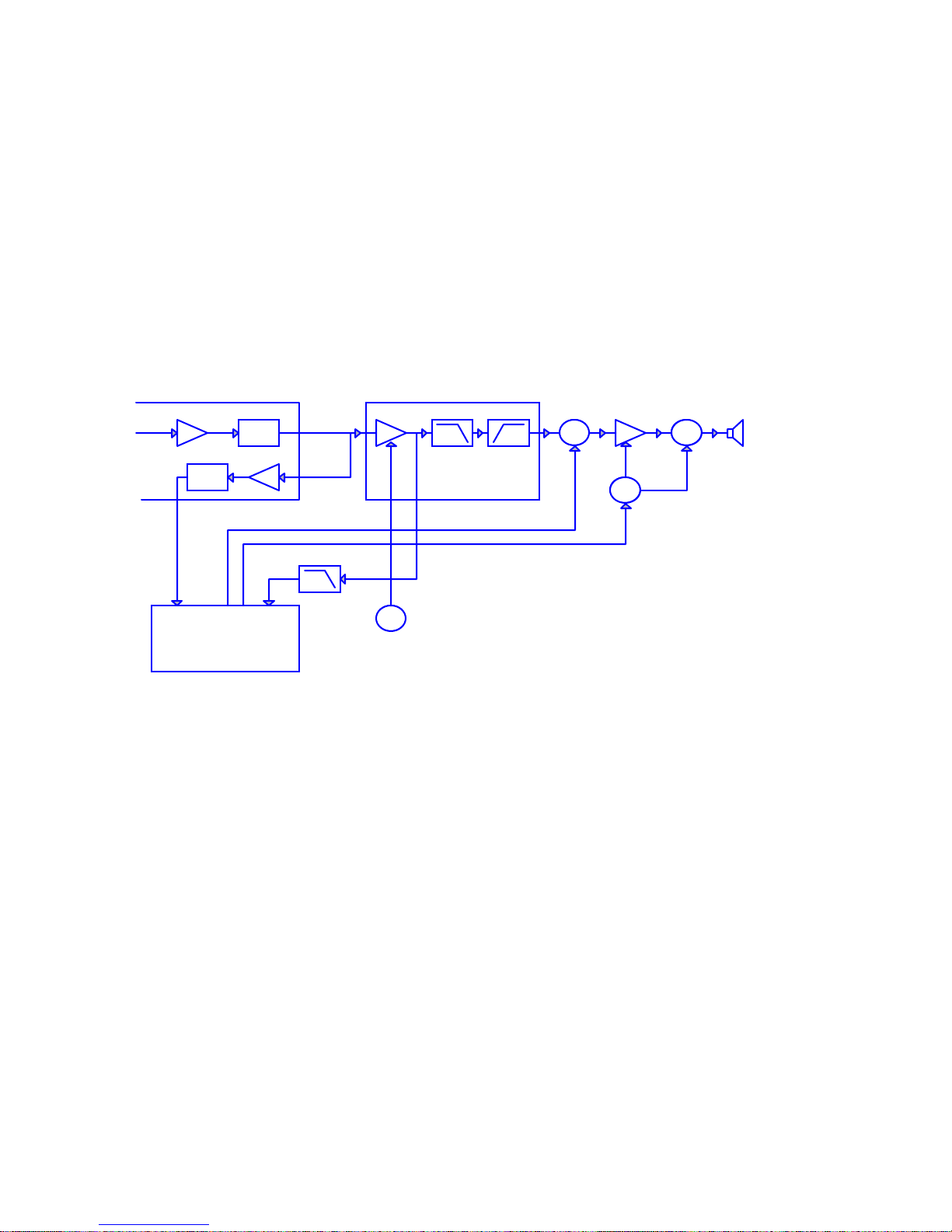
RPU416A Circuit Description
signal. The second IF signal is then fed through a 450kHz ceramic filter (CF200) to further eliminate
unwanted
4) AF
The recovered AF signal obtai ned from IC200 is amplified by I C300 (1/4), filtered by the I C300 low-pass
filter (2/4) and IC300 high-pass filter (3/4) and (4/4), and de-emphasized by R303 and C306. The AF
signal is then passed through a WIDE/NARROW switc h ( Q 303) . The processed AF signal passes t hro ugh
an AF volume control and is amplified to a sufficient level to drive a loud speaker by an AF pow er amplifier
(IC302).
5) Squelch
Part of the AF signal from the IC enter s the FM IC agai n, and t he noise c ompone nt is amplif ied and
rectif ied by a filter and an amplifier to produce a DC voltage corresponding to the noise level.
The DC signal from the FM IC goes t o the ana log por t of the microprocessor (I C403). IC403 deter mines
whether to output sounds fr om the speaker, IC403 sends a high sig nal to the MUTE and AFCO lines and
turns IC302 on through Q302, Q304, Q305, Q306 and Q307. (See Fig.3)
signals befor e it is amplified and FM det ected in IC200.
amplifier
FM IF IC200
IF AMP DET
DET HPF
AMP
IC 300
AF AMP LPF HPF
Q302SWIC302
AF/PF AMP
Q307
SW
Q304.Q305.Q306
SW
SP
IC301
LPF
IC403
MPU
MUTE
AFCO
562676
TI
Q303
W/N SW
BUSY
Fig. 3. AF Amplifier and squelch
6) Receiving signaling
QT/DQT
300 Hz and higher audio frequencies of the output signal from IF IC are cut by a low-pass filter (I C301).
The resulting signal enters the microprocessor (IC403). IC403 determines whether the QT or DQT
matches the preset value, a nd controls t he M UTE and AFCO and t he s peaker o utp ut sounds according to
t he s quel ch r esults.
3. PLL frequency synthesizer
The PLL circuit generates the first local oscillat or signal for r ec ept ion and the RF signal for tr ansmission.
1) PLL
The frequency step of t he PLL circuit is 5 or 6.25kHz. A 12.8MHz reference oscillator s ignal is divided at
IC1 by a fixed counter to produce the 5 or 6.25kHz reference fr equency. The voltage controlled oscil lator
(VCO) output signal is buffer amplified by Q 6, then divided in IC1 by a dual-mod ule
RPU416A Circuit Description
programmable counter. The divided signal is compared i n phase with the 5 or 6.25kHz reference signal in
the phase comparator i n IC1. The output signal from the phase comparator is filter ed t hrough a low- pass
filter and passed to t he VCO to control the oscillator f r equency. (See Fig. 4 of Next Page)
5
Page 6

C
PLL DATA
REF OSC
I/N
I/M
PLL IC IC1
5KHz/6.25KHz
PHASE
COMPARATOR
5KHz/6.25KHz
CHARGE
PUMP
LPF
D2.4Q4TX VCO
D1.3Q3RX VCO
Q6
BUFF AMP
Q5.7
T/R SW
Q2
RF AMP
DD
C
B
12.8MHz
B
Fig. 4. PLL circuit
2) VCO
The operati ng frequency is generated by Q4 in transmit mode and Q3 in receive mode. The oscillator
frequency is controlled by apply ing the VCO control volt age, obtained from the phase comparator, to t he
varactor diodes (D2 and D4 in transmit mode and D1 and D3 in receive mode) . The T/R pi n is set hig h i n
receive mode causing Q5 and Q7 to turn Q4 off, and turn Q3 on. T he T/R pin is set low in transmit mode.
The outputs fr om Q3 and Q4 are amplified by Q6 and sent to the buffer amplifiers.
3) UNLOCK DETECT OR
If a pulse signal appears at t he LD pin of I C1, an unlock conditio n occurs, and the DC voltage obtai ned
from D7, R6, and C1 causes t he voltage applied to t he UL pin of t he microprocessor to go low. When the
microprocessor detects this condition, the transmitter is disabled, ignoring the push-to-talk switch input
signal. (See Fig. 5)
5C
R6
IC1
PLL IC
D7
LD
C1
IC403
UL
MPU
4. Transmitter
1) Transmit audio
The modulatio n signal from the microphone is amplified by IC500 (1/ 2), passes through a pr eemphasis
circuit, and amplified by the ot her IC500 (1/2) to perform IDC operation. The sig nal then passes thro ugh a
low-pass f ilter (splatt er filter) (Q501 and Q502) and cuts 3kHz and higher frequencies.
6
Fig. 5. Unlock detector circ uit
Page 7
RPU416A Circuit Description
ANT
The resulting sig nal goes to the VCO through the VCO mod ulation terminal for direct FM modulation. ( See
Fig. 6)
2) QT/ DQT encoder
A necessary signal for QT/DQT encoding is generated by IC403 and FM-modulated to the PLL
refer ence signal. Since the refer ence OSC does not mod ulate the loop characterist ic frequency or higher,
modulatio n is perfor med at t he VCO side by adjusting the balance. ( See Fig. 6)
IC500(1/2)
MIC
AMP PREEMPHASIS
IC500(1/2)
IDC
Q501.502
LPF
(SPLATTER FILTER)
VR501
MAX
DEV D5.Q4
MIC
Q503
SW
MUTE
IC403
TO
QT/DQT
VR500
BALANCE
VCO
X1.IC1
REFERENCE
OSC
Fig. 6. Transmit audio QT/DQT
3) RF amplifier
The transmit signal obtai ned from the VCO buffer amplifier Q100, is amplified by Q101 and
Q102. This amplified signal is passed to the power amplifier, Q105 and Q107, w hich consists of a 2-stage
FET amplifier a nd is capable of produci ng up to 4W of RF power (See Fig. 7-b)
AMP
D
C
Q101.102
5T
DET
Q103.Q104
B SW
DRIVE AMP
Q105
APC
IC100
Q109
SW
FINAL AMP
Q107
ANT SW
D101 LPF
B
B
APC
TH102
5T
A
SW
Q110
4) ANT switch and LPF
The RF amplifier output signal is passed t hro ugh a low-pass filter networ k and a transmit/receive
5T
Q108
SW
5T
Fig. 7 APC system
Q106
SW
ANT SW
D102.103
RX
Title
Number RevisionSize
7
Page 8

RPU416A Circuit Description
switching circuit before it is passed to the antenna terminal. The transmit/receive switching circuit is
comprised of D101, D102 and D103. D102 and D103 turned on (conductive ) in transmit mode and off
(isolated) in receive mode.
5) APC
The automatic power control (APC) circuit stabilizes the transmitter output power at a predetermined
level by sensing the drai n curre nt of the final amplifier Field Effect Transistor (FET). The voltage obtai ned
from the above drain current with a reference voltage which is set using the microprocessor. An APC
voltage proport ional to t he difference betw een the sensed voltage and the reference voltage appears at
the o utput of IC100 (1/ 2). This output voltage co ntrols t he gate of t he FET power amplifier, which keeps
the transmitter output power can be varied by the microprocessor which in turn changes the reference
voltage and hence , the output pow er.
6) Terminal protect io n circuit
When the thermistor (TH102) reaches about 80", the protection circuit turns on Q110 to protect
transmitt ing final amplifier ( Q 107) .
5. Power supply
A 5V reference power supply [5M] for the control circuit is derived from an internal battery. This
refer ence is used to provide a 5V supply in transmit mode [5T] ,a 5V supply in receive mode [5R] , and a
5V, supply common in both modes [5C] based on the control signal sent
from the microprocessor.
6. Control system
The IC403 CPU operates at 7.37MHZ. This osc illator has a circuit t hat shift s the frequency accordi ng to
the EEPROM data.
8
Page 9

RPU416A Software Specifications
.Specifications:
1. Use mechanical knob to choose fr om 16 channels.
Frequency ra nge: UHF: 450~470MHz
2. Monitor
3. Auto power saving
4. Audio alarm
5. Aut o s quelc h control ( 0~9 level)
6. Timing
7. Channel space 25kHz/12.5kHz(Wide/ Narrow )
8. CTCSS & DQT enc ode
9. CTCSS & DQT decode
10.Two Tone Signal decode
11.Two Tone Signal encode
12.Busy channel lock
13.Clock frequency de viat io n
14.Scan
15.PC mode
16.PC modifying mode
17.Wire clone
18.Manual modifying mode
.Description:
1. User mode: general radio mode
2. PC mode:
Make settings through external programmer or PC progr am soft ware:
(1) Receive frequency & Transmit frequency
(2) Receive signaling & Transmit signaling
(3) Lock busy cha nnel
(4) Clock frequency deviation
(5) Timing
(6) Squelch leve l s e le c tivit y
(7) Power saving
(8) Audio Alarm
(9) Channel space 25kHz/12.5kHz(Wide/Narr ow)
(10) Monitor mode
(11) Scan mode
(12) Reset scan mode
(13) Scan priority
3. PC mod ify mode:
Make settings through external programmer or PC progr am soft ware:
RPU416A Software Specifications
(1) Frequency stability
(2) RF power
(3) Low power alarm
(4) Squelch (level 9&3)
(5) CTCSS deviation (Wide/Narrow).
(6) DQT devi ation (Wide/ Narrow).
(7) Receive sensitivity(low"medium"high)
4. Wire Clone:
Press MO NI to turn on the power , enter wir e clone mode 2 seconds later, press PTT,
Begin cloning while red lights, f inis h while light goes out.
5. Mode setting:
(1) Shor t cut t he SELF on PCB, and tur n o n the power till “BEEP” .
(2) Set c hannel selector knob to corr esponding place according to the model(1-16)
9
Page 10

(3) Press [MONI],then press [PTT], to set the cha nnel, channel data and initial data.
(4) Turn off the power, disconnect SELF on PCB to end mode sett ings.
(5) Remarks:
The old data(frequency, CTCSS/DQT, channel function) will be deleted once set the new
mode by pressing MONI AND PTT , part of the function also would be changed. Therefore, do
not set this operation unless change the EEPROM, etc.
10
Page 11

11
RPU416A Software Specifications
(6) TC- 368(2) channel freque ncy diagra m (af ter setting):
1CH 2CH(Central) 3CH(L) 4CH(H)
No Model Frequency(MHz)
Initial
(MHz)
IF(MHz)
Tx(MHz) Rx(MHz) Tx(MHz) Rx(MHz) Tx(MHz) Rx(MHz) Tx(MHz) Rx(MHz)
1 136.000~149.995 140.000 +38.85 143.100 143.100 143.000 143.100 136.000 136.100 149.975 149.900
2 150.000~173.995 150.000 +38.85 162.100 162.100 162.000 162.100 150.000 150.100 173.975 173.900
3 400.000~419.995 410.000 -38.85 410.100 410.100 410.000 410.100 400.000 400.100 419.975 419.900
4 RPU416A 450.000~469.995 450.000 -38.85 460.100 460.100 460.000 460.100 450.000 450.100 469.975 469.900
5 350.000~369.995 360.000 -38.85 360.100 360.100 360.000 360.100 350.000 350.100 369.975 369.900
6 370.000~389.995 380.000 -38.85 380.100 380.100 380.000 380.100 370.000 370.100 389.975 389.900
7 220.000~239.995 230.000 -38.85 230.100 230.100 230.000 230.100 220.000 220.100 239.975 239.900
8 240.000~259.995 250.000 -38.85 250.100 250.100 250.000 250.100 240.000 240.100 259.975 259.900
9 406.000~429.995 410.000 -38.85 418.100 418.100 418.000 418.100 406.000 406.100 429.975 429.900
10 144.000~147.995 145.000 +38.85 146.100 146.100 146.000 146.100 144.000 144.100 147.975 147.900
11 336.000~367.995 350.000 -38.85 352.100 352.100 352.000 352.100 336.000 336.100 367.975 367.900
12 268.000~395.995 380.000 -38.85 382.100 382.100 382.000 382.100 268.000 268.100 395.975 395.900
13 430.000~439.995 430.000 -38.85 435.100 435.100 435.000 435.100 430.000 430.100 439.975 439.900
14 438.000~449.995 440.000 -38.85 444.100 444.100 444.000 444.100 438.000 438.100 449.975 449.900
15 465.000~494.995 480.000 -38.85 480.100 480.100 480.000 480.100 465.000 465.100 494.975 494.900
16 490.000~519.995 500.000 -38.85 505.100 505.100 505.000 505.100 490.000 490.100 519.975 519.900
Initialization data of channel ar e in the above diagram CH1-CH4, the modify f requency is reset t o initial data. Frequency of C H5~CH14 are the same with CH1.
The sig naling of CH5 and CH10 is 67.0Hz; the signaling of CH6 and CH11 is 151.4 Hz; the signaling of CH7, CH12 is 250.3Hz; the signaling of CH8 and CH13 is
423(DQT); t he signaling of CH9 and CH14 is -423(DQT). CH1~CH9 are Wide, CH10~C H14 are Narrow.
RPU416A
Page 12

RPU416A Software Specifications
6. Manual Adjust Mode:
Press PTT and MONI simultaneously to turn on the power"enter manual Adjust mode out 3
seconds later. Choose the settings by turning the channel selector knob 1-12CH, use PTT
(upward) or MONI (downward) to adjust (Notice: MIC shouldn’t be connected w ith exter nal cable
while modifying), 1~ 12CH are define d as f ollows :
(1) Frequency stabilit y
(2) RF power
(3) Low power alarm
(4) Receiver sensitivity (center f r equency adjust)
(5) Receiver sensitivity (low frequency adjust)
(6) Receiver sensitivity (high frequency adjust)
(7) Squelch (level 9)
(8) Squelch (level 3)
(9) CTCSS deviation (Wide)
(10) CTCSS dev iation ( Narrow )
(11) DQT deviatio n (Wide)
(12) DQT deviatio n (Narr o w)
13~16CH are used for adjusti ng trans mitter and recei ver. Press PTT to transmit; Pr ess MO NI
to choose: Wide/Narr ow, one Beep sound is Narrow, two Beep sound is W ide. 13~16CH are
defined as follows:
(13) center f r equency (discr epancy of tr ansmissio n and recei ve frequency is 0.1MHz).
(14) Low est f r equency (discrepancy of t r ansmission and recei ve frequency is 0.1MHz).
(15) Highest f r equency (discrepancy of tr ansmission and recei ve frequenc y is -0.075MHz).
(16) center f requency: sends 250.3 Hz CTCSS sig nals (discrepancy of t ransmission and receive
frequency is 0.1MHz).
Note:
To enter and shut off manual adjust mode by short cut the SELF. Turn on the power, and enter
settings mode, the manual function is automati call y on. Press [PTT] to disable manual modif y. Once
this function is disabled, this mode is not accessibl e, kindly suggest di sable this mode after adjust.
. CPU:
CPU control M38034M 4
Pin No. Port
name
1 TI I Input QT/DQT signal
2 BUSY I Input busy signal
3 BATT I Detect battery voltage
4NCINC
5 TO O Output QT/DQT
6 BEEP O Beep output
7NCINC
8 ENC0 I Input encode
9 ENC1 I Input encode
10 ENC2 I Input encode
11 ENC3 I Input encode
12 NC I NC
13 PTT I [PTT] input ,connect RXD
14 TXD O RS-232C output
RPU416A Software Specifications
15 RXD I RS-232C input
x16 MONI I [MONI] input
17 SELF I Program L: set up mode
18 CNVSS I Connect VSS
19 RST I Reset
20 INT0 I Power detection
21 NC I NC
22 XIN I Oscillator(7.3728MHz)
I/O Function
12
Page 13

23 XOUT O Oscillator
24 VSS I Grounding
25 SHIFT O Clock frequency deviation H: unlock
26 PABC O MOS FET power H: unlock
27 WNRC O Audio referential sensitivity L: narrow
28 WNTC O Max deviation H: narrow
29 NC I NC
30 SDA I/O EEPROM data cable
31 SCL O EEPROM clock cable
32 UL I Lock circuit detector L: unlock
33 DT O Common data output
34 CK O Common clock output
35 LE O PLL IC H: lock up
36 5MC O Power control except CPU and EEPROM L: unlock
37 AFCO O AF amplifier H: unlock
38 RX O TX/RX VCO H: receive
39 GLED O Green light control H: light
40 RLED O Red light control H: light
41 SAVE O Power saving control H: power saving OFF
42 MUTE O Squelch control H: mic squelch L:AF squelch
43 5RC O Receiver power control L: unlock
44 5TC O Transmitter power control H: unlock
45 NC I NC
46 NC I NC
47 NC I NC
48 NC I NC
49 NC I NC
50 NC I NC
51 NC I NC
52 NC I NC
53 NC I NC
54 NC I NC
55 VCCN O Frequency output
56 APC O TX:auto frequency output RX:BPF tune output
57 VCC I CPU input power 5V
58 VREF I Connect with VCC
59 AVSS I Connect with VSS
60 NC I NC
61 NC I NC
62 NC I NC
63 NC I NC
64 TIBI I QT/DQT exterior circuit central point input
13
Page 14

RPU416 A Adjust Descriptio n
Use programmer or PC software to program RPU416A, or by manual program, refer to”RPU416A
software description ” for the manual program and mode settings.
. Instrument:
1. Synthesized test instrume nt 1 set
2. Scanner 1 set
3. 3A/10V power 1 set
4. Digital Voltmeter 1 set
5. 3A DC Ammeter 1 set
. Adjust:
1. Initiali zat ion
It is necessary to init ialize the t ranscei ver because there is useless data in EEPROM . Short cut the
SELF o n PCB, t urn on the pow er till there comes t he sound ”BEEP”, place the channel selector
knob, press [M O NI], then press [PTT], to begin initializing the channel and other data. Please r ef er
to the outcome of initialization at”RP U416A sof t w are description”.
2.Adjustment:
The adj ustment of RPU416A, some are conducted in normal mode, some are i n manual program
mode. Turn on the power and ent er the normal mode., at t he same time, pr ess the PTT and MONI
to turn on the transceiver"enter the manual program mode 3seconds later.(refer to”RPU416A
software description” manual program mode).
VCO SECT ION:
measurement Adjustment
ITEM CONDITION
Test equip terminal part Method
Specifications/
Remarks
1.Setting 1.power 7.5V
2.Transmit
VCO lock
voltage
3.Receive
VCO lock
voltage
1.CH: TX HIGH 3.7V±0.1V
2.CH: TX LOW check RPU416A >1V
1.CH: RX HIGH 3.7V±0.1V
2.CH: RX LOW
Digital
Volt meter
CV TC1
check
RPU416A>1V
Note:
If unlock VCO, check adjustment is enabled in manual mode.( signal c ould be transmitted regardl es s of the
lock of VCO in manual mode).
14
Page 15

RPU416 A Adjust Descriptio n
Adjust the r eceiver sect ion:
Item Condition
1:CH:RX center
turn to channel 4 in
manual mode
4.Bandpass
filter
5.Sensitivity
(Wide)
2. CH: RX LOW
turn to channel 5 in
manual mode
3.CH:RX HIGH
turn to channel 6 in
manual mode
1. CH:RX center
Turn to channel 13 in
manual mode
Dev : Wide
2. CH: RX center
Turn to channel 14 in
manual mode
Dev : Wide
3. CH: RX center
Turn to channel 15 in
manual mode
Dev : Wide
(enter manual mode)
Measurement Adjustment
Test equip Terminal parts Method
Adjust the undee to the top,
the bandwidth is about
10MHz, the sign of central
frequency is in the middle of
the undee
Adjust the undee to the top to
receive
Low frequency , the sign is on
the left of the top of the undee
Adjust the undee to the top to
receive
High frequency , the sign is on
the right of the top of the
undee
check
Spectrum
analyzer
Synthetical
test
SSG output :
-118dBm
MOD:1kHz
DEV:±3kHz
FILER: 0.3-
3.4kHz
ANT . TP2
ANT
SP
TC202
TC203
PTT(up)
MONI
(down)
PTT(up)
MONI
(down)
Specifications
/Remarks
SINAD: 12dB
or higher
6.Sensitivity
(Narrow)
7.Squelch
1. CH: RX center
Turn to channel 13 in
manual mode
Dev : narrow
2. CH: RX center
Turn to channel 14 in
manual mode
Dev : narrow
3. CH: RX center
Turn to channel 15 in
manual mode
dev : narrow
1.CH: RX center
Turn to channel 7 in
manual mode
2.CH:RX center
Turn to channel 8 in
manual mode
Synthetical
test
SSG output :
-116dBm
MOD:1kHz
DEV:±1.5kH
z FILER:
0.3-3.4kHz
Synthetical
test SSG
output : -
117dBm
Synthetical
test SSG
output : -
125dBm
ANT
SP
ANT
SP
PTT(up)
MONI
(down)
check
Level 9
Adjust to close the squelch.
Level 3
Adjust to close the squelch.
SINAD: 12dB
or higher
The squelch
must be closed
The squelch
must be closed
15
Page 16

RPU416 A Adjust Descriptio n
3
3
3
3
6
Adjust the t r ansmitter sect ion:
Item Condition
Test equip Terminal Parts Method
Measurement Adjustment
Specifications
/Remarks
8.Transmit
frequency
9.Power
10.MAX
DEV
CH: TX center
Turn to channel 1 in
manual mode
1.CH:TX center
Turn to channel 2 in
manual mode
2.CH: TX LOW
Turn to channel 3
Press PTT
3.CH:TX HIGH
Turn to channel 4
Press PTT
1.CH: TX center,
turn to channel 1
in manual mode,
dev: wide
Press PTT
2.CH: TX center,
turn to channel 1
in manual mode,
dev: narrow
Press PTT
Synthetical
test
Synthetical
test
Ammeter
Synthetical
test LPF:
15kHz
AF:1kHz
120mV
ANT
ANT
ANT
MIC
PTT(up)M
ONI(down)
PTT(up)M
ONI(down)
VR501 Adjust it to:4.2kHz±100Hz Wide
Adjust it to center frequency Error<150Hz
Adjust it to:
3.7<Po<
3.7<Po<
3.7<Po<
Check:1.8kHz-2.2kHz Narrow
4.5W
I<1.6A
Adjust it to:
4.5 W
I<1.6A
Adjust it to:
4.5W
I<1.6A
11.MIC
SENS
12.DQT/QT
13.QT DEV
1.CH: TX center,
turn to channel 1
in manual mode,
dev: wide
Press PTT
2.CH: TX center,
turn to channel 1
in manual mode,
dev: narrow
Press PTT
1.CH: TX center,
turn to channel 9 in
manual mode
2.CH: TX center,
turn to channel 1
in manual mode,
press PTT
1.CH: TX center,
turn to channel 9 in
manual mode
Synthetical
test
FILER:
0.3-3.4kHz
AF:1kHz
12mV
Synthetical
test LPF:
300Hz
Synthetical
test
LPF:300Hz
VR501 Check:2.2kHz-3.6kHz Wide
ANT
MIC
ANT VR500
ANT
PTT"up"M
ONI"down
"
Check:1.1kHz-1.8kHz Narrow
Adjust VR500,the test value of
on condition 1 & condition 2 is
consistent, the difference
value<20Hz
Adjust it to:0.75kHz±50Hz Wide
67.0Hz
CTCSS
250.3Hz
CTCSS
16
Page 17

RPU416 A Adjust Descriptio n
0
2
3
A
y
14.DQT DEV
15.Low
Battery level
2.CH: TX center,
turn to channel 1
in manual mode
1.CH: TX center,
turn to channel 11
in manual mode
2.CH:TX center,
turn to channel 1
in manual mode
Turn to channel
in manual mode,
djust the batter
to 5.8V
Synthetical
test
LPF:300H
Digital
voltmeter
ANT
"
PTT"up"M
ONI"down
"
PTT"up"M
ONI"down"Adjust so that the LED flashes
Adjust it to:0.35kHz±50Hz Narrow
Adjust it to:0.75kHz±50Hz Wide
Adjust it to:0.35kHz±50Hz Narrow
"
Note:
In manual mode , channel selector 1-12, MIC can’t connect li ne, after adjust compl ete, short SELF, enter
mode settingpress PTT, disable m anual adjust.
17
Page 18

Disassembly for Repair
Separating the case assembly from the chassis
1. Remove the two knobs # and three round nuts $.
2. Remove the two screws %.
3. Expand the right and left sides of the bottom of the case asse mbly"lift the chassis, and remove it from the case
assembly.
4. Taking care not to cut the speaker lead, open the chassis and case assembly.
Removi ng the le ver
Raise the lever on the lower case, insert a small flat screwdriver into the space between the case and lever , open the
case carefully and lift the lever off .
Note: Do not force to separate the case from the lever.
18
Page 19

Exploded View
Packing
19
Page 20

20
Page 21

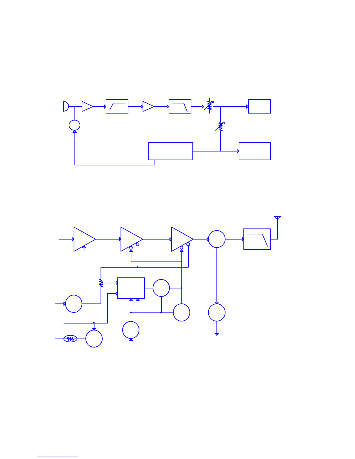
RPU416A Level Diagram
Rx Section
SG output level for obtaining 12Db/SINAD when injected to each point Modulate the AF level with a frequency of 1kHz and deviation of 1.5kHz
through a 470pF coupling capacitor. (Narrow), 3kHz(Wide) . Then take the signal form the signal generator
Measure the 1
st
Local level on a RF VTVM. when the AF output has been adjusted to 0.63Vrms with the AF vo l .
Tx Section
Measure the audio frequency on an AFVTVM and radio frequency on a RF VTVM at high impedance . Set t he MIC input to obtain a modulatio n factor of 60%
with the transmit frequency at center and a modulatio n frequency of 1kHz .
ANT
L112
C145
R22 4
5R
L20 3, L21 4
1st Local
0.1Vrms
IC200
C212
Q201
R21 0
SP
Q307
IC302
VR
IC300
-116.5dBm -113dBm -98dBm -103dBm -104dBm -106.5dBm -103dBm 1018mVrms 175mVr ms 23. 5mVrms 0.63Vrms
L20 8
RF cen ter IF 38.85MHz
AF 1kHz
Q202
R21 1
R21 7
XF200
Q203
VR50 1
IC500
MIC
Q4
Q6
Q100
Q101 Q102
AF VTVM RF VTVM
Q107
Q105
C114C108C106
C100
C40
D5
ANT
4W
16mVrms 430mVrms 310mVrms 0.15Vrms 0.44Vrms
0.8Vrms
0.62Vrms
Page 22

Main Technical Specific ations
Frequency range 450 MHz ~470 MHz
Channel 16
Channel space 25kHz / 12.5kHz
Antenna impedance 50
Transmitter
impedance
Input voltage 7.2V DC
Frequency stability ±2.5×10
Frequency stability ±2.5×10
Output power 4.0±0.5W
Operating sensitivity 12±3mV
Audio distortion 5%
Modulation limiting 5kHz / 2.5kHz
2K&
-6
Transmitter
-6
Bandwidth 16 kHz/8kHz
Modulate specialty '3dB
Spurious RF 7.5(W
Adjacent power -65 d B / -55dB
Receiver
Reference sensitivity Precede 0.28(V / 0.35(V
Squelch turnon
sensitivity
Audio frequency 500mW
Audio deviation 7%
Operating bandwidth "±7 kHz"/"±3.5 kHz"
Audio response +2dB -8dB
Channel restrain -8 d B
Obstruct 85d B
Selectivity 65 d B / 60dB
0.4(V
Spurious response 60 d B
Intermodulation 60 d B
22
 Loading...