Page 1

8
8G
t
Memory Module Specifications
HX434C19FW2/8
HX434C19FW2/
8GB 1G x 64-Bit
B 1G x 64-Bi
DDR4-3466 CL19 288-Pin DIMM
SPECIFICATIONS
DESCRIPTION
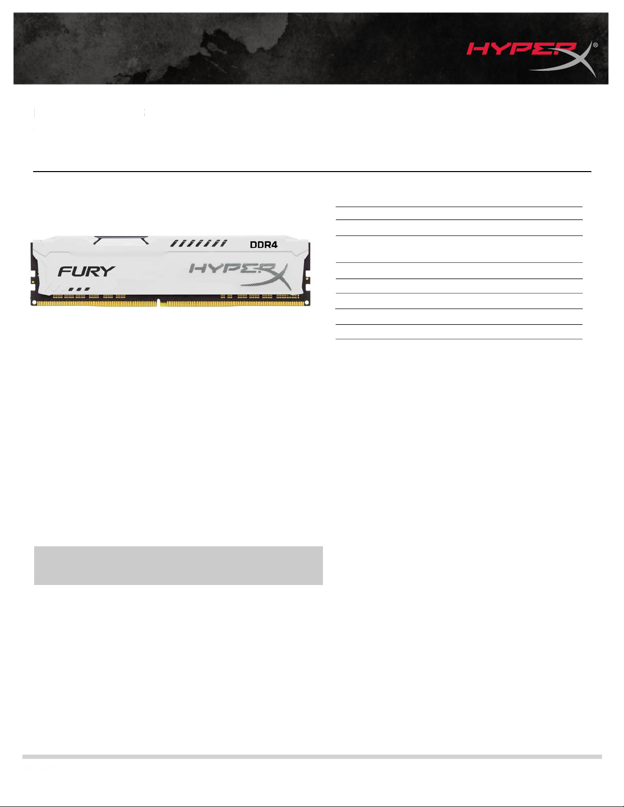
HyperX HX434C19FW2/8 is a 1G x 64-bit (8GB) DDR4-3466 CL19
SDRAM (Synchronous DRAM) 1Rx8, memory module, based on
eight 1G x 8-bit FBGA components per module.
supports Intel® Extreme Memory Profiles (Intel® XMP) 2.0.
Each module has been tested to run at DDR4-3466 at a low latency
timing of 19-23-23 at 1.2V.
shown in the Plug-N-Play (PnP) Timing Parameters section
below. The JEDEC standard electrical and mechanical
specifications are as follows:
Additional timing parameters are
Each module
CL(IDD)
Row Cycle Time (tRCmin)
Refresh to Active/Refresh
Command Time (tRFCmin)
Row Active Time (tRASmin)
Maximum Operating Power
UL Rating
Operating Temperature
Storage Temperature
*Power will vary depending on the SDRAM used.
19 cycles
45.75ns(min.)
350ns(min.)
24.234ns(min.)
TBD W*
94 V - 0
o
C to +85o C
0
o
C to +100o C
-55
FEATURES
• Power Supply: VDD = 1.2V Typical
• VDDQ = 1.2V Typical
• VPP = 2.5V Typical
• VDDSPD = 2.2V to 3.6V
• On-Die termination (ODT)
• 16 internal banks; 4 groups of 4 banks each
• Bi-Directional Differential Data Strobe
• 8 bit pre-fetch
kingston.com/hyperx
hyperxgaming.com
Note: The PnP feature offers a range of speed and timing options to support
the widest variety of processors and chipsets. Your maximum speed will
be determined by your BIOS.
JEDEC/XMP TIMING PARAMETERS
• JEDEC/PnP: DDR4-3466 CL19-23-23 @1.2V
•XMP Profile #1: DDR4-3466 CL19-23-23 @1.2V
•XMP Profile #2: DDR4-2933 CL17-19-19 @1.2V
• Burst Length (BL) switch on-the-fly BL8 or BC4(Burst Chop)
• Height 1.340” (34.04mm), w/heatsink
Continued >>
Document No. 4808607A 02/15/18 Page 1
Page 2

±
continued
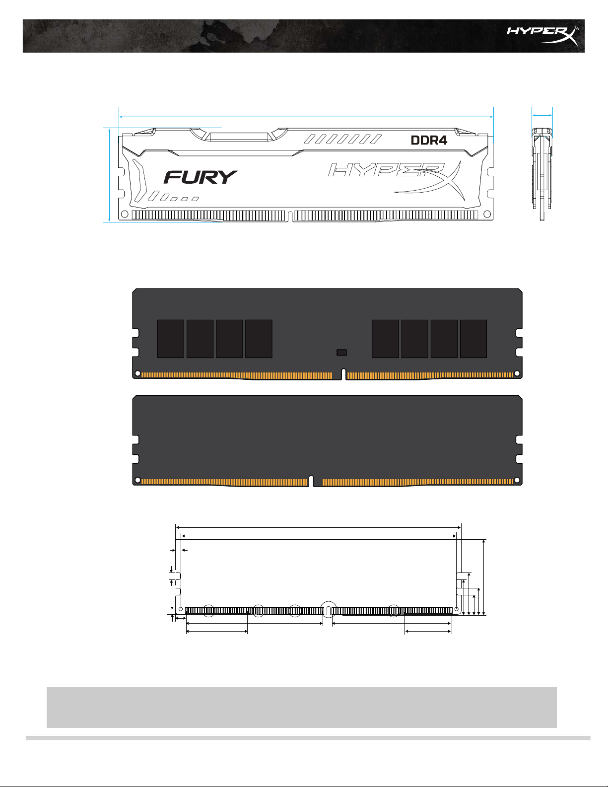
MODULE WITH HEAT SPREADER
7.08 mm
133.35 mm
34.04 mm
MODULE DIMENSIONS
All measurements are in millimeters.
(Tolerances on all dimensions are ±0.12 unless otherwise specified)
133.35
129.55
2.10±0.15
3.00
Detail A
Pin 1
0.15
3.35
2.70
The product images shown are for illustration purposes only and may not be an exact representation of the product.
Kingston reserves the right to change any information at anytime without notice.
28.90
Detail B Detail D Detail C
Pin 35 Pin 47
64.60
Detail E
FOR MORE INFORMATION, GO TO HYPERXGAMING.COM
All Kingston products are tested to meet our published specifications. Some motherboards or system configurations may not operate at
the published HyperX memory speeds and timing settings. Kingston does not recommend that any user attempt to run their computers
the published HyperX memory speeds and timing settings. Kingston does not recommend that any user attempt to run their computers
faster than the published speed. Overclocking or modifying your system timing may result in damage to computer components.
faster than the published speed. Overclocking or modifying your system timing may result in damage to computer components.
HyperX is a division of Kingston.
©2018 Kingston Technology Corporation, 17600 Newhope Street, Fountain Valley, CA 92708 USA.
All rights reserved. All trademarks and registered trademarks are the property of their respective owners.
Pin 105 Pin 117
56.10
22.95
31.25
11.00
8.00
17.60
14.60
Document No. 4808607A Page 2
hyperxgaming.com
 Loading...