Page 1

8
8G
t
Memory Module Specifications
HX424C15FB2/8
HX424C15FB2/
8GB 1G x 64-Bit
B 1G x 64-Bi
DDR4-2400 CL15 288-Pin DIMM
SPECIFICATIONS
DESCRIPTION
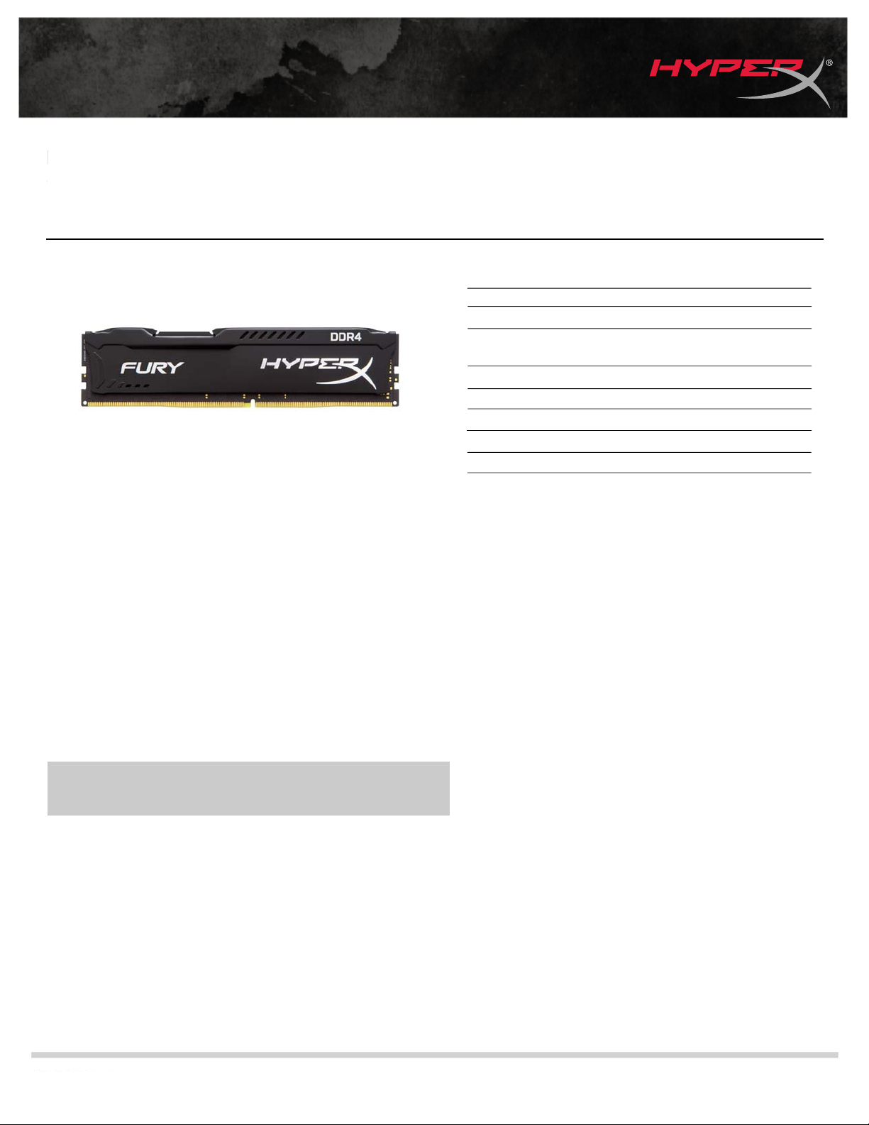
HyperX HX424C15FB2/8 is a 1G x 64-bit (8GB) DDR4-2400 CL15
SDRAM (Synchronous DRAM) 1Rx8, memory module, based on
eight 1G x 8-bit FBGA components per module.
supports Intel® Extreme Memory Profiles (Intel® XMP) 2.0.
Each module has been tested to run at DDR4-2400 at a low latency
timing of 15-15-15 at 1.2V.
shown in the Plug-N-Play (PnP) Timing Parameters section
below. The JEDEC standard electrical and mechanical
specifications are as follows:
Note: The PnP feature offers a range of speed and timing options to support
the widest variety of processors and chipsets. Your maximum speed will
be determined by your BIOS.
Additional timing parameters are
Each module kit
JEDEC/XMP TIMING PARAMETERS
• JEDEC/PnP: DDR4-2400 CL15-15-15 @1.2V
DDR4-2133 CL14-14-14 @1.2V
•XMP Profile #1: DDR4-2400 CL15-15-15 @1.2V
CL(IDD)
Row Cycle Time (tRCmin)
Refresh to Active/Refresh
Command Time (tRFCmin)
Row Active Time (tRASmin)
Maximum Operating Power
UL Rating
Operating Temperature
Storage Temperature
*Power will vary depending on the SDRAM used.
15 cycles
46.75ns(min.)
350ns(min.)
29.125ns(min.)
TBD W*
94 V - 0
o
C to +85o C
0
o
C to +100o C
-55
FEATURES
• Power Supply: VDD = 1.2V Typical
• VDDQ = 1.2V Typical
• VPP - 2.5V Typical
• VDDSPD = 2.2V to 3.6V
• Nominal and dynamic on-die termination (ODT) for
data, strobe, and mask signals
• Low-power auto self refresh (LPASR)
• Data bus inversion (DBI) for data bus
• On-die VREFDQ generation and calibration
• Single-rank
• On-board I2 serial presence-detect (SPD) EEPROM
• 16 internal banks; 4 groups of 4 banks each
• Fixed burst chop (BC) of 4 and burst length (BL) of 8
via the mode register set (MRS)
• Selectable BC4 or BL8 on-the-fly (OTF)
• Fly-by topology
• Terminated control command and address bus
• Height 1.340” (34.04mm), w/o heatsink
kingston.com/hyperx
hyperxgaming.com
Continued >>
Document No. 4807667-001.A00 03/18/16 Page 1
Document No. 4807667-001.A00 03/18/16 Page 1
Page 2

±
continued
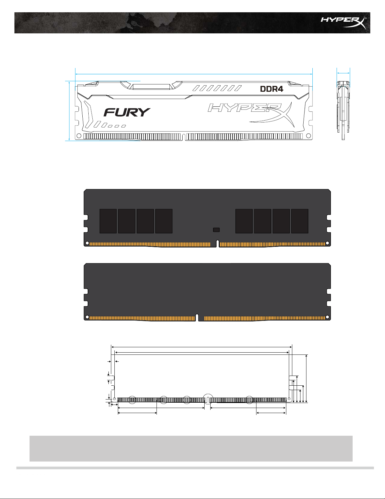
MODULE WITH HEAT SPREADER
7.08 mm
133.35 mm
34.04 mm
MODULE DIMENSIONS
133.35
129.55
2.10
±±0.15
3.00
Detail A
Pin 1
0.15
3.35
2.70
28.90
Detail B Detail D Detail C
Pin 35 Pin 47
64.60
Detail E
FOR MORE INFORMATION, GO TO HYPERXGAMING.COM
All Kingston products are tested to meet our published specifications. Some motherboards or system configurations may not operate at
the published HyperX memory speeds and timing settings. Kingston does not recommend that any user attempt to run their computers
the published HyperX memory speeds and timing settings. Kingston does not recommend that any user attempt to run their computers
faster than the published speed. Overclocking or modifying your system timing may result in damage to computer components.
faster than the published speed. Overclocking or modifying your system timing may result in damage to computer components.
HyperX is a division of Kingston.
©2016 Kingston Technology Corporation, 17600 Newhope Street, Fountain Valley, CA 92708 USA.
All rights reserved. All trademarks and registered trademarks are the property of their respective owners.
Pin 105 Pin 117
56.10
31.25
11.00
8.00
17.60
14.60
22.95
Document No. 4807667-001.A00 Page 2
hyperxgaming.com
 Loading...