


hyper
stone
32-Bit-RISC/DSP Microprocessor
E1-32XS / E1-16XS
User's Manual

Specifications and information in this document are subject to change
without notice and do not represent a commitment on the part of
Hyperstone AG. Hyperstone AG reserves the right to make changes to
improve functioning. Although the information in this document has been
carefully reviewed, Hyperstone AG does not assume any liability arising
out of the use of the product or circuit described herein.
Hyperstone AG does not authorize the use of the Hyperstone
microprocessor in life support applications wherein a failure or
malfunction of the microprocessor may directly threaten life or cause
injury. The user of the Hyperstone microprocessor in life support
applications assumes all risks of such use and indemnifies Hyperstone
AG against all damages.
No part of this manual may be reproduced or transmitted in any form or
by any means, electronic or mechanical, including photo-copying and
recording, for any purpose without the permission of Hyperstone AG.
Hyperstone is a registered trademark of Hyperstone AG
For further information please contact:
Hyperstone AG
Line-Eid-Strasse 3
D-78467 Konstanz
Germany
Phone (+49) 7531 / 9803-0
Fax (+49) 7531 / 51725
E-Mail info@hyperstone.de
www.hyperstone.com
Copyright 1990..2004 Hyperstone AG
Revision 02/2004

Table of Contents
Table of Contents
1. ARCHITECTURE...................................................................................................... 1-1
1.1. INTRODUCTION ....................................................................................................... 1-1
1.1.1. Compatibility:................................................................................................. 1-2
1.1.2. Phased Locked Loop: ..................................................................................... 1-2
1.1.3. Registers:........................................................................................................ 1-2
1.1.4. Flags:.............................................................................................................. 1-2
1.1.5. Register Data Types: ...................................................................................... 1-3
1.1.6. External Memory:........................................................................................... 1-3
1.1.7. On-Chip Memory (IRAM): ............................................................................. 1-3
1.1.8. Memory Data Types: ...................................................................................... 1-3
1.1.9. Runtime Stack:................................................................................................ 1-3
1.1.10. Instruction Cache: ........................................................................................ 1-3
1.1.11. Instructions General:.................................................................................... 1-3
1.1.12. Instruction Summary: ................................................................................... 1-4
1.1.13. Exceptions: ................................................................................................... 1-5
1.1.14. Timer: ........................................................................................................... 1-6
1.1.15. Bus Interface: ............................................................................................... 1-6
1.1.16. Power Management: .................................................................................... 1-6
1.2. B
LOCK DIAGRAM ................................................................................................... 1-7
1.3. G
LOBAL REGISTER SET .......................................................................................... 1-8
1.3.1. Program Counter PC ..................................................................................... 1-9
1.3.2. Status Register SR......................................................................................... 1-10
1.3.3. Floating-Point Exception Register FER....................................................... 1-13
1.3.4. Stack Pointer SP ........................................................................................... 1-13
1.3.5. Upper Stack Bound UB ................................................................................ 1-13
1.3.6. Bus Control Register BCR............................................................................ 1-13
1.3.7. Timer Prescaler Register TPR...................................................................... 1-14
1.3.8. Timer Compare Register TCR ...................................................................... 1-14
1.3.9. Timer Register TR......................................................................................... 1-14
1.3.10. Watchdog Compare Register WCR ............................................................ 1-14
1.3.11. Input Status Register ISR............................................................................ 1-14
1.3.12. Function Control Register FCR ................................................................. 1-14
1.3.13. Memory Control Register MCR.................................................................. 1-14
1.4. LOCAL REGISTER SET........................................................................................... 1-15
1.5. P
RIVILEGE STATES ............................................................................................... 1-16
1.6. R
EGISTER DATA TYPES ........................................................................................ 1-17
1.7. M
1.8. S
1.9. I
1.10. O
EMORY ORGANIZATION..................................................................................... 1-18
TACK .................................................................................................................. 1-20
NSTRUCTION CACHE............................................................................................ 1-25
N-CHIP MEMORY (IRAM) ............................................................................... 1-27
2. INSTRUCTIONS GENERAL ................................................................................... 2-1
2.1. I
NSTRUCTION NOTATION ........................................................................................ 2-1
2.2. I
NSTRUCTION EXECUTION ...................................................................................... 2-2
2.3. I
NSTRUCTION FORMATS.......................................................................................... 2-3
2.3.1. Table of Immediate Values ............................................................................. 2-5
2.3.2. Table of Instruction Codes ............................................................................. 2-6
2.3.3. Table of Extended DSP Instruction Codes ..................................................... 2-7

Table of Contents
2.4. ENTRY TABLES....................................................................................................... 2-8
2.5. I
NSTRUCTION TIMING........................................................................................... 2-12
3. INSTRUCTION SET ................................................................................................. 3-1
3.1. M
EMORY INSTRUCTIONS ........................................................................................ 3-1
3.1.1. Address Modes ............................................................................................... 3-2
3.1.1.1. Register Address Mode:.......................................................................... 3-2
3.1.1.2. Postincrement Address Mode: ................................................................ 3-2
3.1.1.3. Displacement Address Mode: ................................................................. 3-2
3.1.1.4. Absolute Address Mode:......................................................................... 3-2
3.1.1.5. I/O Displacement Address Mode:........................................................... 3-3
3.1.1.6. I/O Absolute Address Mode: .................................................................. 3-3
3.1.1.7. Next Address Mode:................................................................................ 3-4
3.1.1.8. Stack Address Mode: .............................................................................. 3-4
3.1.1.9. Address Mode Encoding:........................................................................ 3-5
3.1.2. Load Instructions ........................................................................................... 3-6
3.1.3. Store Instructions ........................................................................................... 3-8
3.2. M
3.3. M
3.4. L
3.5. I
3.6. M
3.7. A
3.8. S
3.9. S
3.10. N
3.11. M
3.12. M
3.13. D
3.14. S
OVE WORD INSTRUCTIONS................................................................................ 3-10
OVE DOUBLE-WORD INSTRUCTION................................................................... 3-10
OGICAL INSTRUCTIONS....................................................................................... 3-11
NVERT INSTRUCTION........................................................................................... 3-12
ASK INSTRUCTION............................................................................................. 3-12
DD INSTRUCTIONS.............................................................................................. 3-13
UM INSTRUCTIONS.............................................................................................. 3-15
UBTRACT INSTRUCTIONS .................................................................................... 3-16
EGATE INSTRUCTIONS...................................................................................... 3-17
ULTIPLY WORD INSTRUCTION......................................................................... 3-18
ULTIPLY DOUBLE-WORD INSTRUCTIONS ........................................................ 3-18
IVIDE INSTRUCTIONS ....................................................................................... 3-19
HIFT LEFT INSTRUCTIONS................................................................................. 3-20
3.15. SHIFT RIGHT INSTRUCTIONS............................................................................... 3-21
3.16. R
3.17. I
OTATE LEFT INSTRUCTION............................................................................... 3-22
NDEX MOVE INSTRUCTIONS .............................................................................. 3-23
3.18. CHECK INSTRUCTIONS........................................................................................ 3-24
3.19. N
3.20. C
O OPERATION INSTRUCTION ............................................................................ 3-24
OMPARE INSTRUCTIONS ................................................................................... 3-25
3.21. COMPARE BIT INSTRUCTIONS............................................................................. 3-26
3.22. T
3.23. S
3.24. S
3.25. B
3.26. D
3.27. C
3.28. T
3.29. F
3.30. R
3.31. F
3.32. E
3.33. S
EST LEADING ZEROS INSTRUCTION .................................................................. 3-26
ET STACK ADDRESS INSTRUCTION ................................................................... 3-27
ET CONDITIONAL INSTRUCTIONS...................................................................... 3-27
RANCH INSTRUCTIONS ..................................................................................... 3-29
ELAYED BRANCH INSTRUCTIONS ..................................................................... 3-30
ALL INSTRUCTION ............................................................................................ 3-32
RAP INSTRUCTIONS .......................................................................................... 3-33
RAME INSTRUCTION ......................................................................................... 3-35
ETURN INSTRUCTION........................................................................................ 3-37
ETCH INSTRUCTION .......................................................................................... 3-39
XTENDED DSP INSTRUCTIONS ......................................................................... 3-40
OFTWARE INSTRUCTIONS ................................................................................. 3-42
3.33.1. Do Instruction ............................................................................................ 3-43
3.33.2. Floating-Point Instructions........................................................................ 3-44

Table of Contents
4. EXCEPTIONS ............................................................................................................ 4-1
4.1. EXCEPTION PROCESSING ........................................................................................ 4-1
4.2. E
XCEPTION TYPES .................................................................................................. 4-2
4.2.1. Reset ............................................................................................................... 4-2
4.2.2. Range, Pointer, Frame and Privilege Error .................................................. 4-2
4.2.3. Extended Overflow ......................................................................................... 4-3
4.2.4. Parity Error .................................................................................................... 4-3
4.2.5. Interrupt.......................................................................................................... 4-3
4.2.6. Trace Exception.............................................................................................. 4-4
4.3. EXCEPTION BACKTRACKING................................................................................... 4-4
5. TIMER AND CPU CLOCK MODES ...................................................................... 5-1
5.1. OVERVIEW.............................................................................................................. 5-1
5.1.1. Timer Prescaler Register TPR........................................................................ 5-1
5.1.2. Timer Register TR........................................................................................... 5-2
5.1.3. Timer Compare Register TCR ........................................................................ 5-3
5.1.4. Power-Down Mode......................................................................................... 5-3
5.1.5. Additional Power Saving................................................................................ 5-4
5.1.6. Sleep Mode ..................................................................................................... 5-5
6. BUS INTERFACE...................................................................................................... 6-1
6.1. B
US CONTROL GENERAL ........................................................................................ 6-1
6.1.1. Boot Width Selection ...................................................................................... 6-2
6.1.2. SRAM and ROM Bus Access .......................................................................... 6-2
6.1.3. DRAM Bus Access, Fast Page Mode or EDO DRAM.................................... 6-2
6.1.3.1. DRAM Row Address Bits Multiplexing ................................................. 6-3
6.1.4. SDRAM Bus Access ........................................................................................ 6-4
6.1.4.1. SDRAM Row Address Bits Multiplexing............................................... 6-4
6.1.4.2. SDRAM Mode Register Setting.............................................................. 6-5
6.1.4.3. SDRAM Connection ............................................................................... 6-5
6.2. I/O B
US ACCESS..................................................................................................... 6-6
6.3. BUS CONTROL REGISTER BCR............................................................................... 6-8
6.4. M
EMORY CONTROL REGISTER MCR.................................................................... 6-12
6.4.1. MEMx Parity Disable................................................................................... 6-14
6.4.2. MEM2 Wait Disable ..................................................................................... 6-14
6.4.3. DRAMType and DRAMType2 ...................................................................... 6-15
6.4.4. Entry Table Map........................................................................................... 6-15
6.4.5. MEMx Bus Hold Break................................................................................. 6-15
6.4.6. MEMx Bus Size............................................................................................. 6-15
6.5. SDRAM CONTROL REGISTER SDCR................................................................... 6-16
6.5.1. BankAddrEnable........................................................................................... 6-16
6.5.2. CS1Enable .................................................................................................... 6-16
6.5.3. CS1Select...................................................................................................... 6-17
6.5.4. CASLatency .................................................................................................. 6-17
6.5.5. SDCLKSelect ................................................................................................ 6-17
6.5.6. SDRAM Connection Example....................................................................... 6-17
6.6. INPUT STATUS REGISTER ISR............................................................................... 6-18
6.7. F
UNCTION CONTROL REGISTER FCR.................................................................... 6-19
6.7.1. CLKOUTControl and CLKOUTControl2 .................................................... 6-21
6.8. W
6.9. IO3 C
ATCHDOG COMPARE REGISTER WCR............................................................... 6-21
ONTROL MODES.......................................................................................... 6-21

Table of Contents
6.9.1. IO3Standard Mode....................................................................................... 6-21
6.9.2. Watchdog Mode............................................................................................ 6-21
6.9.3. IO3Timing Mode .......................................................................................... 6-21
6.9.3.1. On IO3Direction = Input:...................................................................... 6-22
6.9.3.2. IO3Direction = Output: ......................................................................... 6-22
6.9.4. IO3TimerInterrupt Mode ............................................................................. 6-22
6.10. B
US SIGNALS...................................................................................................... 6-23
6.10.1. Bus Signals for the E1-32XS Processor ..................................................... 6-23
6.10.2. Bus Signals for the E1-16XS Processor ..................................................... 6-24
6.10.3. Bus Signal Description............................................................................... 6-25
6.11. B
US CYCLES....................................................................................................... 6-30
6.11.1. SRAM and ROM Accesses.......................................................................... 6-30
6.11.1.1. SRAM and ROM Single-Cycle Read Access ..................................... 6-30
6.11.1.2. SRAM Single-Cycle Write Access ..................................................... 6-30
6.11.1.3. SRAM and ROM Multi-Cycle Read Access....................................... 6-31
6.11.1.4. SRAM Multi-Cycle Write Access....................................................... 6-31
6.11.2. MEM2 Read Access with WAIT Pin........................................................... 6-32
6.11.3. I/O Read Access ......................................................................................... 6-33
6.11.4. I/O Read Access with WAIT Pin................................................................. 6-34
6.11.5. I/O Write Access......................................................................................... 6-35
6.11.6. DRAM......................................................................................................... 6-36
6.11.6.1. Fast Page Mode DRAM Access.......................................................... 6-36
6.11.6.2. EDO DRAM Single-Cycle Access ..................................................... 6-37
6.11.6.3. EDO DRAM Multi-Cycle Access....................................................... 6-38
6.11.6.4. Fast Page Mode or EDO DRAM Refresh ........................................... 6-39
6.11.6.5. SDRAM Access .................................................................................. 6-40
6.12. DC C
HARACTERISTICS ....................................................................................... 6-41
6.12.1. Absolute Maximum Ratings........................................................................ 6-41
6.12.2. D.C. Parameters......................................................................................... 6-41
6.13. AC C
HARACTERISTICS ....................................................................................... 6-42
6.13.1. Processor Clock and CLKIN...................................................................... 6-42
6.13.2. GRANT# response time .............................................................................. 6-42
7. MECHANICAL DATA ............................................................................................. 7-1
HYPERSTONE E1-32XS, 144-PIN LQFP PACKAGE.................................................. 7-1
7.1.
7.1.1. Pin Configuration - View from Top Side........................................................ 7-1
7.1.2. Pin Cross Reference by Pin Name ................................................................. 7-2
7.1.3. Pin Cross Reference by Location................................................................... 7-3
7.2. HYPERSTONE E1-16XS, 100-PIN LQFP PACKAGE.................................................. 7-4
7.2.1. Pin Configuration - View from Top Side........................................................ 7-4
7.2.2. Pin Cross Reference by Pin Name ................................................................. 7-5
7.2.3. Pin Cross Reference by Location................................................................... 7-6
HYPERSTONE E1-32XSB, 144-PIN TFBGA PACKAGE............................................ 7-7
7.3.
7.3.1. Pin Configuration – View from Top Side....................................................... 7-7
7.3.2. Pin Cross Reference by Pin Name ................................................................. 7-8
7.3.3. Pin Cross Rreference by Location ................................................................. 7-9
HYPERSTONE E1-16XSB, 100-PIN TFBGA PACKAGE.......................................... 7-10
7.4.
7.4.1. Pin Configuration – View from Top Side..................................................... 7-10
7.4.2. Pin Cross Reference by Pin Name ............................................................... 7-11
7.4.3. Pin Cross Rreference by Location ............................................................... 7-12
ACKAGE DIMENSIONS......................................................................................... 7-13
7.5. P

Table of Contents
7.5.1. Package Dimensions LQFP ......................................................................... 7-13
7.5.2. Package Dimensions TFBGA ....................................................................... 7-15


E1-32XS User’s Manual Page 1-1
1. Architecture
1.1. Introduction
The hyperstone E1-32XS and hyperstone E1-16XS microprocessors represent a further
development of the hyperstone E1-32X and hyperstone E1-16X processors. Using a
sophisticated 0.25 µm CMOS process, the maximum clock rate of the processor could be
further improved. Being pin-compatible to their predecessors these new processors can be
used as a direct replacement in existing designs, given that the changed voltage supply
requirements are considered.
This combination of a high-performance RISC microprocessor with an additional powerful
DSP instruction set and on-chip microcontroller functions offers a high throughput. The
speed is obtained by an optimized combination of the following features:
❒ The most recent stack frames are kept in a register stack, thereby reducing data memory
accesses to a minimum by keeping almost all local data in registers.
❒ Pipelined memory access allows overlapping of memory accesses with execution.
❒ 16 KByte fully static On-Chip Memory (IRAM).
❒ On-chip Instruction Cache omits instruction fetch in inner loops and provides prefetch.
❒ Variable-length instructions of 16, 32 or 48 bits provide a large, powerful instruction
set, thereby reducing the number of instructions to be executed.
❒ Primarily used 16-bit instructions halve the memory bandwidth required for instruction
fetch in comparison to conventional RISC architectures with fixed-length 32-bit
instructions, yielding also even better code economy than conventional CISC
architectures.
❒ Orthogonal instruction set.
❒ Most instructions execute in one cycle.
❒ Pipelined DSP instructions.
❒ Parallel execution of ALU, DSP, and load/store instructions.
❒ Single-cycle half-word multiply-accumulate operation.
❒ Fast Call and Return by parameter passing via registers.
❒ An instruction pipeline depth of just two stages — decode/execute — provides
branching without insertion of wait cycles in combination with Delayed Branch
instructions.
❒ Range and pointer checks are performed without speed penalty, thus, these checks need
no longer be turned off, thereby providing higher runtime reliability.
❒ Separate address and data buses provide a throughput of one 32-bit word each cycle.
The features noted above contribute to reduce the number of idle wait cycles to a bare
minimum. The processor is designed to sustain its execution rate with a standard SDRAM
memory.
The low power consumption is of advantage for mobile (portable) applications or in
temperature-sensitive environments.

Page 1-2 Architecture
Most of the transistors are used for the on-chip memory, the instruction cache, the register
stack and the multiplier, whereas only a small number is required for the control logic.
Due to their low manufacturing costs, the
hyperstone E1-32XS and E1-16XS
microprocessors are very well suited for embedded systems applications requiring high
performance and lowest cost. To simplify board design as well as to reduce system costs,
the hyperstone E1-32XS and E1-16XS already come with integrated peripherals, such as a
timer and memory and bus control logic. Therefore, complete systems using hyperstone
microprocessors can be designed with a minimum of external components. To connect any
kind of memory or I/O, no glue logic is necessary. It is even suitable for systems where up
to now microprocessors with 16-bit architecture have been used for cost reasons. Its
improved performance compared to conventional microcontrollers can be used to
software-substitute many external peripherals like graphics controllers or DSPs. Using the
hyperstone E1-32XS as a core for ASICs or ASSPs is particularly advantageous because the
total gate count of the entire logic is just about 35k gates without the on-chip memory.
The software development tools include an optimizing C compiler, assembler, source-level
debugger with profiler as well as a runtime kernel and a sophisticated DSP library. Using
the runtime kernel, up to 31 tasks, each with its own virtual timer, can be developed
independently of each other. The synchronization of these tasks is effected almost
automatically by the runtime kernel. For the system designer, it seems as if he has up to 31
hyperstone microprocessors to which he can allocate his programs accordingly. Real-time
debugging of multiple tasks is assisted in an optimized way. The DSP library provides a
powerful set of DSP related functions and is taking care of all parallelism between ALU,
DSP, and Load/Store unit.
The following description gives a brief architectural overview:
1.1.1. Compatibility:
❒ Pin compatible to hyperstone E1-32X and hyperstone E1-16X.
1.1.2. Phased Locked Loop:
❒ An internal phased locked loop circuit (PLL) provides clock rate multiplication by a
factor ½, 1, 2, 4, or 8. For example, only an external crystal of 12 MHz is required to
achieve an internal clock rate of 96 MHz.
1.1.3. Registers:
❒ 32 global and 64 local registers of 32 bits each
❒ 16 global and up to 16 local registers are addressable directly
1.1.4. Flags:
❒ Zero(Z), negative(N), carry(C) and overflow(V) flag
❒ Interrupt-mode, interrupt-lock, trace-mode, trace-pending, supervisor state, cache-mode
and high global flag

E1-32XS User’s Manual Page 1-3
1.1.5. Register Data Types:
❒ Unsigned integer, signed integer, single or double signed short, signed complex short,
single or double 16-bit fixed-point, bit string, IEEE-754 floating-point, each either 32 or
64 bits
1.1.6. External Memory:
❒ Address space of 4 Gbytes, divided into five areas
❒ Separate I/O address space
❒ Load/Store architecture
❒ Pipelined memory and I/O accesses
❒ High-order data located and addressed at lower address (big endian)
❒ Instructions and double-word data may cross DRAM page boundaries
1.1.7. On-Chip Memory (IRAM):
❒ 16 KByte fully static internal memory, 32 bit wide, single cycle access
1.1.8. Memory Data Types:
❒ Unsigned and signed byte (8 bit)
❒ Unsigned and signed half-word (16 bit), located on half-word boundary
❒ Undedicated word (32 bit), located on word boundary
❒ Undedicated double-word (64 bit), located on word boundary
1.1.9. Runtime Stack:
❒ Runtime Stack is divided into memory part and register part
❒ Register part is implemented by the 64 local registers holding the most recent stack
frame(s)
❒ Current stack frame (maximum 16 registers) is always kept in register part of the stack
❒ Data transfer between memory and register part of the stack is automatic
❒ Upper stack bound is guarded
1.1.10. Instruction Cache:
❒ An on-chip Instruction Cache reduces instruction memory access substantially
1.1.11. Instructions General:
❒ Variable-length instructions of one, two or three half-words halve required memory
bandwidth
❒ Pipeline depth of only two stages, assures immediate refill after branches
❒ Register instructions of type "source operator destination ⇒ destination" or

Page 1-4 Architecture
"source operator immediate ⇒ destination"
❒ All register bits participate in an operation
❒ Immediate operands of 5, 16 and 32 bits, zero- or sign-expanded
❒ Large address displacement of up to 28 bits
❒ Two sets of signed arithmetical instructions: instructions set or clear either only the
overflow flag or trap additionally to a Range Error routine on overflow
❒ DSP instructions operate on 16-bit integer, real and complex fixed-point data and 32-bit
integer data into 32-bit and 64-bit hardware accumulators
1.1.12. Instruction Summary:
❒ Memory instructions pipelined to a depth of two stages, trap on address register equal to
zero (check for invalid pointers)
❒ Memory address modes: register address, register post-increment, register + dis-
placement (including PC relative), register post-increment by displacement (next
address), absolute, stack address, I/O absolute and I/O displacement
❒ Load, all data types, bytes and half-words right adjusted and zero- or sign-expanded,
execution proceeds after Load until data is needed
❒ Store, all data types, trap when range of signed byte or half-word is exceeded
❒ Move, Move immediate, Move double-word
❒ Logical instructions AND, AND not, OR, XOR, NOT, AND not immediate, OR
immediate, XOR immediate
❒ Mask source and immediate ⇒ destination
❒ Add unsigned/signed, Add signed with trap on overflow, Add with carry
❒ Add unsigned/signed immediate, Add signed immediate with trap on overflow
❒ Sum source + immediate ⇒ destination, unsigned/signed and signed with trap on
overflow
❒ Subtract unsigned/signed, Subtract signed with trap on overflow, Subtract with carry
❒ Negate unsigned/signed, Negate signed with trap on overflow
❒ Multiply word ∗ word ⇒ low-order word unsigned or signed, Multiply word ∗ word ⇒
double-word unsigned and signed
❒ Divide double-word by word ⇒ quotient and remainder, unsigned and signed
❒ Shift left unsigned/signed, single and double-word, by constant and by content of
register
❒ Shift right unsigned and signed, single and double-word, by constant and by content of
register
❒ Rotate left single word by content of register
❒ Index Move, move an index value scaled by 1, 2, 4 or 8, optionally with bounds check
❒ Check a value for an upper bound specified in a register or check for zero
❒ Compare unsigned/signed, Compare unsigned/signed immediate

E1-32XS User’s Manual Page 1-5
❒ Compare bits, Compare bits immediate, Compare any byte zero
❒ Test number of leading zeros
❒ Set Conditional, save conditions in a register
❒ Branch unconditional and conditional (12 conditions)
❒ Delayed Branch unconditional and conditional (12 conditions)
❒ Call subprogram, unconditional and on overflow
❒ Trap to supervisor subprogram, unconditional and conditional (11 conditions)
❒ Frame, structure a new stack frame, include parameters in frame addressing, set frame
length, restore reserve frame length and check for upper stack bound
❒ Return from subprogram, restore program counter, status register and return-frame
❒ Software instructions, call an associated subprogram and pass a source operand and the
address of a destination operand to it
❒ DSP Multiply instructions:
signed and/or unsigned multiplication ⇒ single and double word product
❒ DSP Multiply-Accumulate instructions:
signed multiply-add and multiply-subtract ⇒ single and double word product sum and
difference
❒ DSP Half-word Multiply-Accumulate instructions:
signed multiply-add operating on four half-word operands ⇒ single and double word
product sum
❒ DSP Complex Half-word Multiply instruction:
signed complex half-word multiplication ⇒ real and imaginary single word product
❒ DSP Complex Half-word Multiply-Accumulate instruction:
signed complex half-word multiply-add ⇒ real and imaginary single word product sum
❒ DSP Add and Subtract instructions:
signed half-word add and subtract with and without fixed-point adjustment ⇒ single
word sum and difference
❒ Floating-point instructions are architecturally fully integrated, they are executed as
Software instructions by the present version. Floating-point Add, Subtract, Multiply,
Divide, Compare and Compare unordered for single and double-precision, and Convert
single ⇔ double are provided.
1.1.13. Exceptions:
❒ Pointer, Privilege, Frame and Range Error, Extended Overflow, Parity Error, Interrupt
and Trace mode exception
❒ Watchdog function
❒ Error-causing instructions can be identified by backtracking, thus allowing a very
detailed error analysis

Page 1-6 Architecture
1.1.14. Timer:
❒ Two multi-functional timers
1.1.15. Bus Interface:
❒ Separate address bus of 26 (E1-32XS) or 22 (E1-16XS) bits and data bus of up to 32 (E1-
32XS
) or 16 bits (E1-16XS) provide a throughput of up to four or two bytes at each clock
cycle, respectively.
❒ Data bus width of 32, 16 or 8 bits, individually selectable for each external memory
area.
❒ 8-bit, 16-bit, and 32-bit boot width selectable via two external pins.
❒ Configurable I/O pins
❒ Internal generation of all memory and I/O control signals
❒ Wait pin function for I/O accesses to peripheral devices.
❒ Wait pin function for memory accesses to address space MEM2.
❒ On-chip DRAM controller supporting Fast-Page-Mode DRAMs, EDO DRAMs, and
synchronous DRAMs (SDRAM).
❒ Up to seven vectored interrupts.
❒ Control function for CLKOUT pin.
1.1.16. Power Management:
❒ Lower power supply current in power-down mode.
❒ Clock-Off function to further reduce power dissipation (Sleep Mode).
❒ PLL settings controllable by software, providing a “gear-up” or “gear-down” within one
clock cycle.
E1-32XS User’s Manual Page 1-7
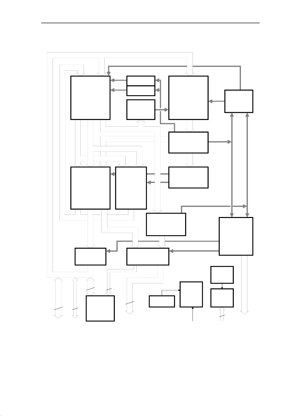
1.2. Block Diagram
Register Set
64 Local
26 Global
X Y PC
X Y I Instruction
ALU
Barrel Shifter
Z W A
X Decode
Y Decode
Instruction
Cache
Control
X Y
DSP
Execution
Unit
Instruction
Cache
Instruction
Decode
Execution
Control
Instruction
Prefetch Control
Load
Decode
Bus Interface
Control
Store Data
Pipeline
32
32
(16)
Data Bus Parity
Figure 1.1: Block Diagram
4
(2)
16 KByte
SRAM
14
Memory Address
Pipeline
26
(22)
Address
Bus
Watchdog
PLL
Power
Reset
Control
Bus Pipeline
Internal
Timer
I/O and
Interrupt
Control
7
Control
Control
Bus

Page 1-8 Architecture
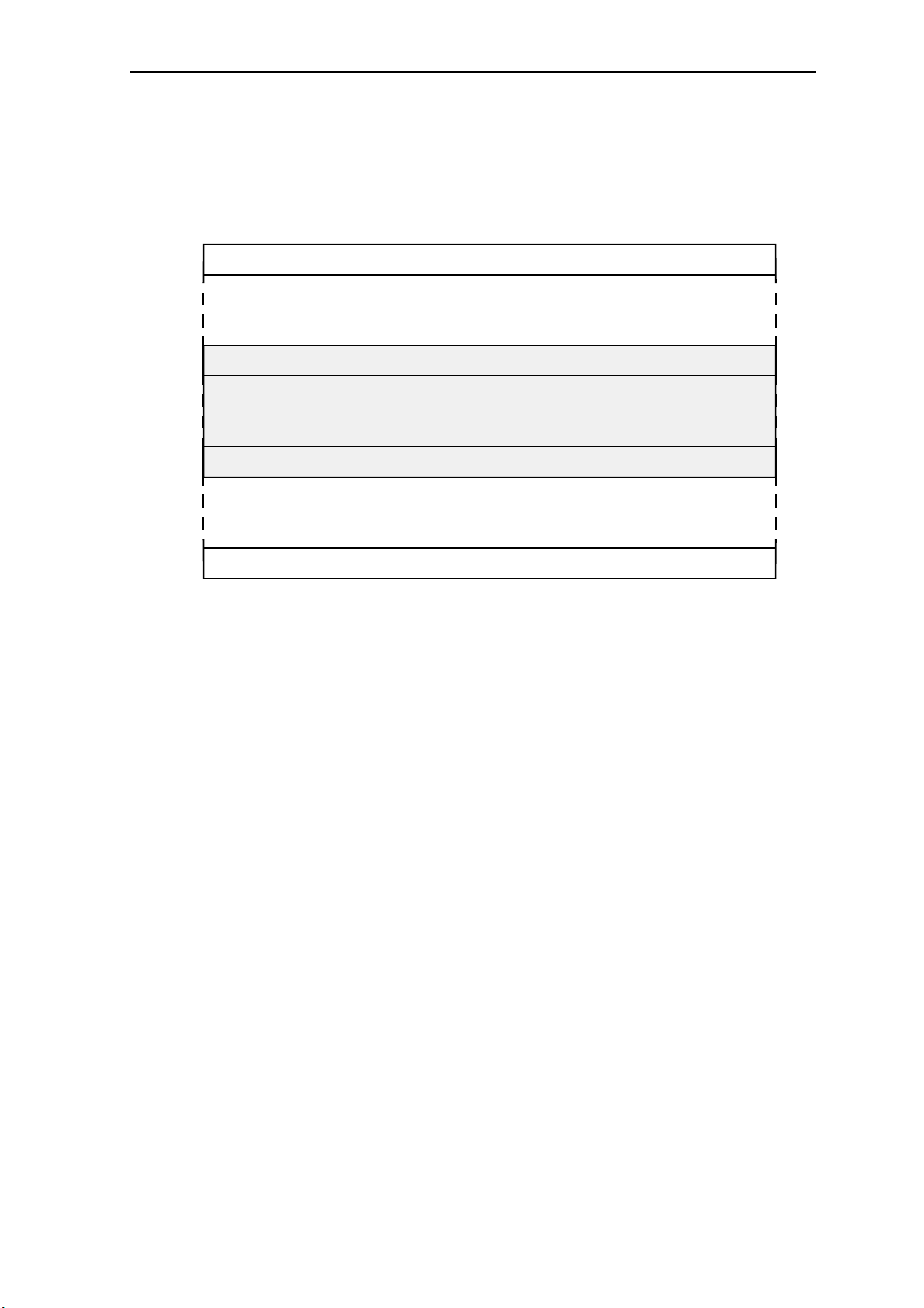
1.3. Global Register Set
The architecture provides 32 global registers of 32 bits each. These are:
G0 Program Counter PC
G1 Status Register SR
G2 Floating-Point Exception Register FER
G3..G15 General purpose registers
G16..G17 Reserved
G18 Stack Pointer SP
G19 Upper Stack Bound UB
G20 Bus Control Register BCR (see section 6. Bus Interface)
G21 Timer Prescaler Register TPR (see section 5. Timer)
G22 Timer Compare Register TCR (see section 5. Timer and CPU Clock
Modes)
G23 Timer Register TR (see section 5. Timer and CPU Clock Modes)
G24 Watchdog Compare Register WCR (see section 6. Bus Interface)
G25 Input Status Register ISR (see section 6. Bus Interface)
G26 Function Control Register FCR (see section 6. Bus Interface)
G27 Memory Control Register MCR (see section 6. Bus Interface)
G28..G31 Reserved
Registers G0..G15 can be addressed directly by the register code (0..15) of an instruction.
Registers G18..G27 can be addressed only by a MOV or MOVI instruction with the high
global flag H set to 1.
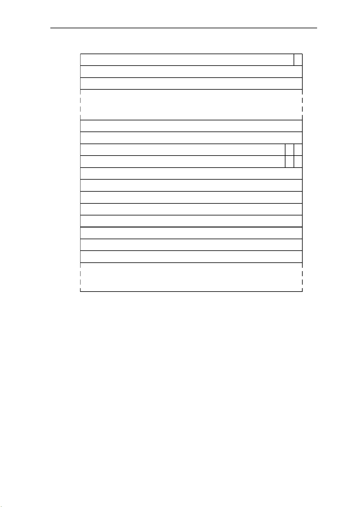
E1-32XS User’s Manual Page 1-9
031
G0
G1
G2
G3
G15
G16
G17
G18
G19
G20
G21
G22
G23
G24
G25
Program Counter PC
Status Register SR
Floating-Point Exception Register FER
General Purpose Registers G3..G15
Reserved
Reserved
Stack Pointer SP
Upper Stack Bound UB
Bus Control Register BCR
Timer Prescaler Register TPR
Timer Compare Register TCR
Timer Register TR
Watchdog Compare Register WCR
Input Status Register ISR
0
0000
G26
G27
G28
G31
Figure 1.2: Global Register Set
Function Control Register FCR
Memory Control Register MCR
G28..G31 Reserved
1.3.1. Program Counter PC
G0 is the program counter PC. It is updated to the address of the next instruction through
instruction execution. Besides this implicit updating, the PC can also be addressed like a
regular source or destination register. When the PC is referenced as an operand, the value
supplied is the address of the first byte after the instruction which references it, except
when referenced by a delay instruction with a preceding delayed branch taken (see section
3.26. Delayed Branch Instructions).
Placing a result in the PC has the effect of a branch taken. Bit zero of the PC is always
zero, regardless of any value placed in the PC.
Page 1-10 Architecture
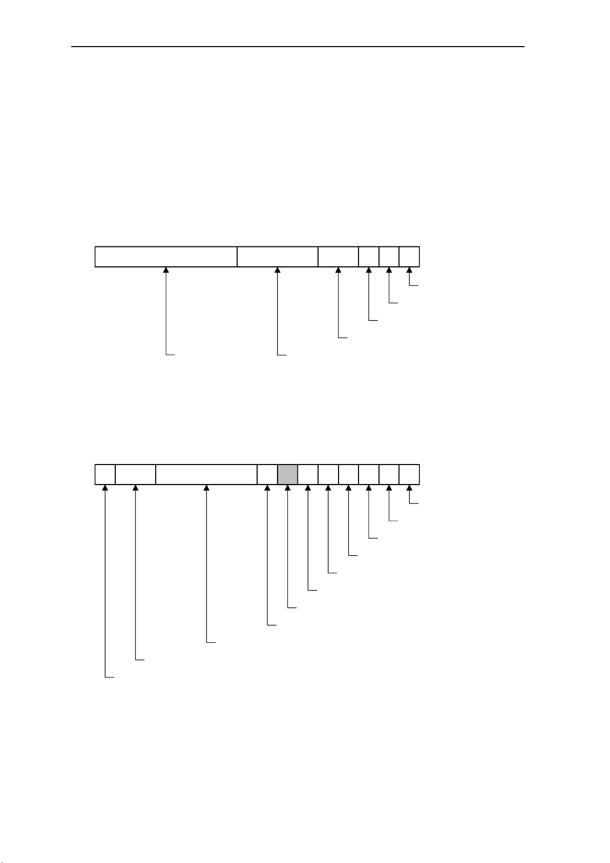
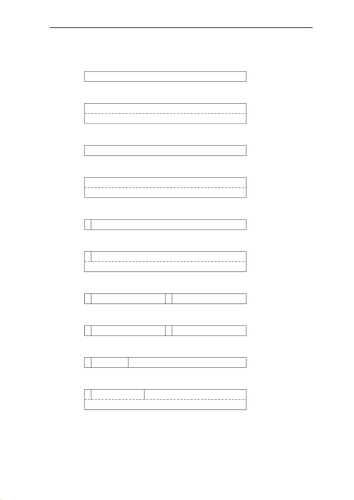
1.3.2. Status Register SR
G1 is the status register SR. Its content is updated by instruction execution. Besides this
implicit updating, the SR can also be addressed like a regular register. When addressed as
source or destination operand, all 32 bits are used as an operand. However, only bits 15..0
of a result can be placed in bits 15..0 of the SR, bits 31..16 of the result are discarded and
bits 31..16 of the SR remain unchanged. The full content of the SR is replaced only by the
Return Instruction. A result placed in the SR overrules any setting or clearing of the
condition flags as a result of an instruction.
31 30 27 26 25 24 23 22 21 20 19 18 17 16
Figure 1.3: Status Register SR (bits 31..16)
1514 11109876543210
L I
FRM
2829
FP
Frame Pointer Frame Length
1213
FTE V N
FL S
ILC
Instruction-Length Code
MH
P
Supervisor State Flag
Z
T
Trace Pending Flag
C
Zero Flag
Trace-Mode Flag
Carry Flag
Floating-Point Trap Enable
Floating-Point Rounding Mode
Interrupt-Lock Flag
Figure 1.4: Status Register SR (bits 15..0)
Negative Flag
Overflow Flag
Cache-Mode Flag
High Global Flag
Reserved
Interrupt-Mode Flag

E1-32XS User’s Manual Page 1-11
The status register SR contains the following status information:
C Bit zero is the carry condition flag C. In general, when set it indicates that the
unsigned integer range has been exceeded. At add operations, it indicates a
carry out of bit 31 of the result. At subtract operations, it indicates a borrow
(inverse carry) into bit 31 of the result.
Z Bit one is the zero condition flag Z. When set, it indicates that all 32 or 64
result bits are equal to zero regardless of any carry, borrow or overflow.
N Bit two is the negative condition flag N. On compare instructions, it indicates
the arithmetic correct (true) sign of the result regardless of an overflow. On all
other instructions, it is derived from result bit 31, which is the true sign bit
when no overflow occurs. In the case of overflow, result bit 31 and N reflect
the inversion of the true sign.
V Bit three is the overflow condition flag V. In general, when set it indicates a
signed overflow.
M Bit four is the cache-mode flag M. Besides being set or cleared under program
control, it is also automatically cleared by a Frame instruction and by any
branch taken except a delayed branch. See section 1.9. Instruction Cache for
details.
H Bit five is the high global flag H. When H is set, denotation of G0..G15 addres-
ses G16..G31 instead. Thus, the registers G18..G27 may be addressed by denoting G2..G11 respectively.
The H flag is effective only in the first cycle of the next instruction after it was
set; then it is cleared automatically.
Only the MOV or MOVI instruction issued as the next instructions can be used
to copy the content of a local register or an immediate value to one of the high
global registers. The MOV instruction can also be used to copy the content of a
high global register (except the BCR, TPR, FCR and MCR register, which are
write-only) to a local register. With all other instructions, the result may be
invalid.
If one of the high global registers is addressed as the destination register in user
state (S = 0), the condition flags are undefined, the destination register remains
unchanged and a trap to Privilege Error occurs.
Reserved Bit six is reserved for future use. It must always be zero.
I Bit seven is the interrupt-mode flag I. It is set automatically on interrupt entry
and reset to its old value by a Return instruction. The I flag is used by the
operating system; it must be never changed by any user program, regardless of
user or supervisor state.
FTE Bits 12..8 are the floating-point trap enable flags (see section 3.33.2. Floating-
Point Instructions).
FRM Bits 14..13 are the floating-point rounding modes (see section 3.33.2. Floating-
Point Instructions).

Page 1-12 Architecture
L Bit 15 is the interrupt-lock flag L. When the L flag is one, all Interrupt, Parity
Error and Extended Overflow exceptions regardless of individual mode bits are
inhibited. The state of the L flag is effective immediately after any instruction
which changed it. The L flag is set to one by any exception.
The L flag can be cleared or kept set in any or on return to any privilege state
(user or supervisor). Changing the L flag from zero to one is privileged to
supervisor or return from supervisor to supervisor state. A trap to Privilege
Error occurs if the L flag is set under program control from zero to one in user
or on return to user state.
The following status information cannot be changed by addressing the SR:
T Bit 16 is the trace-mode flag T. When both the T flag and the trace pending
flag P are one, a trace exception occurs after every instruction except after a
Delayed Branch instruction. The T flag is cleared by any exception.
Note: The T flag can only be changed in the saved return SR and is then
effective after execution of a Return instruction.
P Bit 17 is the trace pending flag P. It is automatically set to one by all in-
structions except by the Return instruction, which restores the P flag from bit
17 of the saved return SR.
Since for a Trace exception both the P and the T flag must be one, the P flag
determines whether a trace exception occurs (P = 1) or does not occur (P = 0)
immediately after a Return instruction which restored the T flag to one.
Note: The P flag can only be changed in the saved SR. No program except the
trace exception handler should affect the saved P flag. The trace exception
handler must clear the saved P flag to prevent a trace exception on return, in
order to avoid tracing the same instruction in an endless loop.
S Bit 18 is the supervisor state flag S (see section 1.5. Privilege States). It is set
to one by any exception.
ILC Bits 20 and 19 represent the instruction-length code ILC. It is updated by
instruction execution. The ILC holds (in general) the length of the last instruction: ILC values of one, two or three represent an instruction length of
one, two or three half-words respectively. After a branch taken, the ILC is
invalid. The Return instruction clears the ILC.
Note: Since a Return instruction following an exception clears the ILC, a
program must not rely on the current value of the ILC.
FL Bits 24..21 represent the frame length FL. The FL holds the number of usable
local registers (maximum 16) assigned to the current stack frame.
FL = 0 is always interpreted as FL = 16.
FP Bits 31..25 represent the frame pointer FP. The least significant six bits of the
FP point to the beginning of the current stack frame in the local register set,
that is, they point to L0.
The FP contains bit 8..2 of the address at which the content of L0 would be
stored if pushed onto the memory part of the stack.
E1-32XS User’s Manual Page 1-13
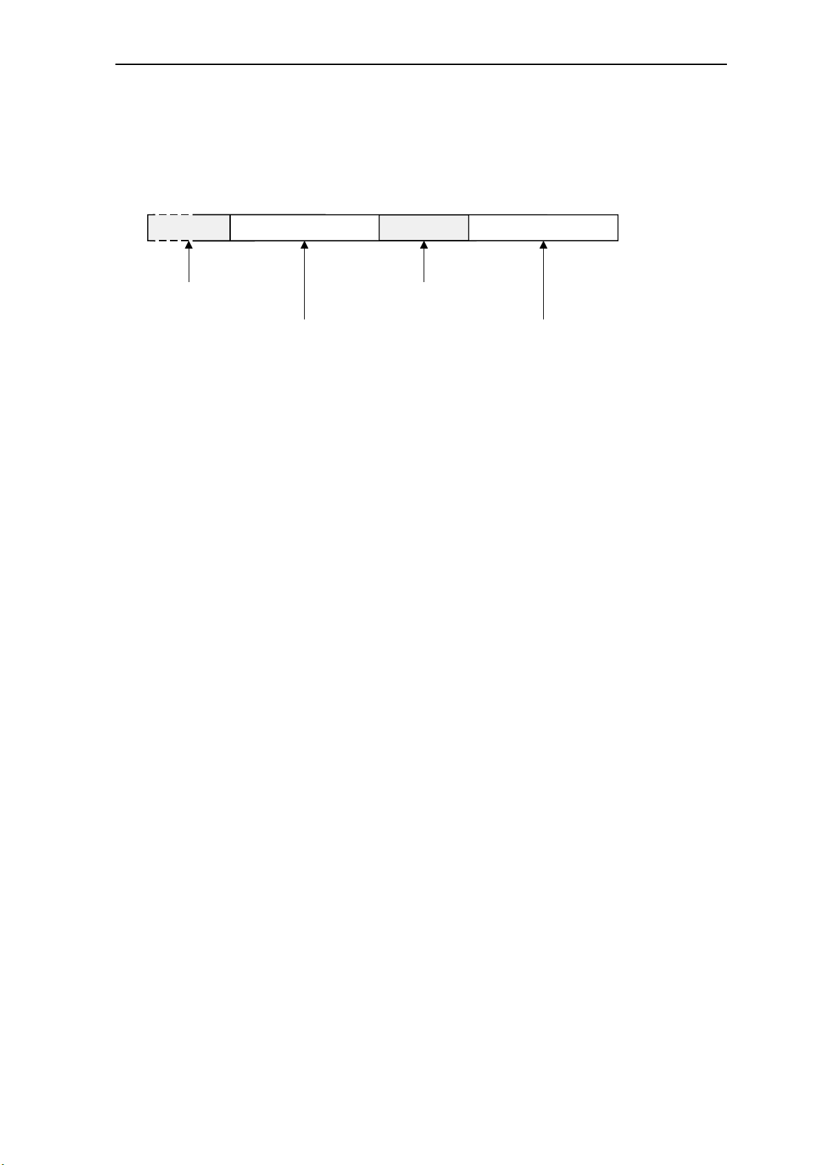
1.3.3. Floating-Point Exception Register FER
G2 is the floating-point exception register. Only bits 12..8 and 4..0 may be changed by a
user program, all other bits must remain unchanged.
31
Reserved
Figure 1.5: Floating-Point Exception Register
1.3.4. Stack Pointer SP
1213 11 10 9 876 5 4
Reserved for Operating System
Floating-Point Actual Exceptions
3
Floating-Point Accrued Exceptions
1 0
2
G18 is the stack pointer SP. The SP contains the top address + 4 of the memory part of the
stack, that is the address of the first free memory location in which the first local register
would be saved by a push operation (see section 3.29. Frame Instruction for details). Stack
growth is from low to high address.
When the SP is set, bits one and zero must always be zero. The SP can be addressed only
via the high global flag H being set. Copying an operand to the SP is a privileged
operation.
1.3.5. Upper Stack Bound UB
G19 is the upper stack bound UB. The UB contains the address beyond the highest legal
memory stack location. It is used by the Frame instruction to inhibit stack overflow.
When the UB is set, bits one and zero must always be zero. The UB can be addressed only
via the high global flag H being set. Copying an operand to the UB is a privileged
operation.
1.3.6. Bus Control Register BCR
G20 is the write-only bus control register BCR. Its content defines the options possible for
bus cycle, parity and refresh control. The BCR can be addressed only via the high global
flag H being set. Copying an operand to the BCR is a privileged operation. The BCR
register is described in detail in the bus interface description in section 6.

Page 1-14 Architecture
1.3.7. Timer Prescaler Register TPR
G21 is the write-only timer prescaler register TPR. It adapts the timer clock to different
processor clock frequencies and controls the processor clock generation by the PLL circuit.
The TPR can be addressed only via the high global flag H being set. Copying an operand
to the TPR is a privileged operation. The TPR is described in the timer description in
section 5. Updating TPR with amended values for the PLL multiplication factor in
conjunction with corresponding updated values for the timer prescaler changes the internal
clock frequency while keeping all timer settings correct.
1.3.8. Timer Compare Register TCR
G22 is the timer compare register TCR. Its content is compared continuously with the
content of the timer register TR. The TCR can be addressed only via the high global flag H
being set. Copying an operand to the TCR is a privileged operation. The TCR is described
in the timer description in section 5.
1.3.9. Timer Register TR
G23 is the timer register TR. Its content is incremented by one on each time unit. The TR
can be addressed only via the high global flag H being set. Copying an operand to the TR
is a privileged operation. The TR is described in the timer description in section 5.
1.3.10. Watchdog Compare Register WCR
G24 is the watchdog compare register WCR. The WCR can be addressed only via the high
global flag H being set. Copying an operand to the WCR is a privileged operation. The
WCR is described in the bus interface description in section 6.
1.3.11. Input Status Register ISR
G25 is the read-only input status register ISR. The ISR can be addressed only via the high
global flag H being set. The ISR is described in the bus interface description in section 6.
1.3.12. Function Control Register FCR
G26 is the write-only function control register FCR. The FCR can be addressed only via
the high global flag H being set. Copying an operand to the FCR is a privileged operation.
The FCR is described in the bus interface description in section 6.
1.3.13. Memory Control Register MCR
G27 is the write-only memory control register MCR. The MCR can be addressed only via
the high global flag H being set. Copying an operand to the MCR is a privileged operation.
The MCR is described in the bus interface description in section 6.
E1-32XS User’s Manual Page 1-15
1.4. Local Register Set
The architecture provides a set of 64 local registers of 32 bits each. The local registers
0..63 represent the register part of the stack, containing the most recent stack frame(s).
0
L0
L15
63
31
0
Local Register L0
Local Register L15
Figure 1.6: Local Register Set 0..63
The local registers can be addressed by the register code (0..15) of an instruction as
L0..L15 only relative to the frame pointer FP; they can also be addressed absolutely as part
of the stack in the stack address mode (see section 3.1.1. Address Modes).
The absolute local register address is calculated from the register code as:
absolute local register address := (FP + register code) modulo 64.
That is, only the least significant six bits of the sum FP + register code are used and thus,
the absolute local register addresses for L0..L15 wrap around modulo 64.
The absolute local register addresses for FP + register code + 1 or FP + FL + offset are
calculated accordingly.

Page 1-16 Architecture
1.5. Privilege States
The architecture provides two privilege states, determined by the supervisor state flag S:
user state (S = 0) and supervisor state (S = 1).
The runtime kernel hyRTK is executed in the higher privileged supervisor state, thereby
restricting access to all sensitive data to a highly reliable system program. The following
operations are also privileged to be executed only in the supervisor or on return from
supervisor to supervisor state:
❒ Copying an operand to any of the high global registers
❒ Changing the interrupt-lock flag L from zero to one
❒ Returning through a Return instruction to supervisor state
Any illegal attempt causes a trap to Privilege Error.
The S flag is also saved in bit zero of the saved return PC by the Call, Trap and Software
instructions and by an exception. A Return instruction restores it from this bit position to
the S flag in bit position 18 of the SR (thereby overwriting the bit 18 returned from the
saved return SR).
If a Return instruction attempts a return from user to supervisor state, a trap to Privilege
Error occurs (S = 1 is saved).
Returning from supervisor to user state is achieved by clearing the S flag in bit zero of the
saved return PC before return. Switching from user to supervisor state is only possible by
executing a Trap instruction or by exception processing through one of the 64 supervisor
subprogram entries (see section 2.4. Entry Tables).
E1-32XS User’s Manual Page 1-17
1.6. Register Data Types
31
MSB
31 0
MSB
Double-Word Bitstring
31
MSB LSB
31
MSB
31
MSB LSB
S
High-Order 32-Bit Magnitude
Unsigned Double-Word Integer
Signed Integer, Two's Complement
32 Bits
Bitstring
High-Order 32-Bits
32-Bit Magnitude
Unsigned Integer
31-Bit Magnitude
LSB
LSBLow-Order 32-Bits
LSBLow-Order 32-Bit Magnitude
0
0
0
0
Register:
n
n
n+1
n
n
n+1
n
31
MSB
S
Signed Double-Word Integer, Two's Complement
31
S MSB LSB S
31
S MSB LSB S
31
S 8-Bit Exponent
31
11-Bit Exponent
S MSB
High-Order 31-Bit Magnitude
15
MSB LSB
Two Signed Shorts
15
Real Part Imaginary Part
Complex Signed Short
MSB LSB
Single Precision Floating-Point Number
Low-Order 32-Bit Fraction
Double Precision Floating-Point Number
MSB LSB
23-Bit Fraction
High-Order 20-Bit Fraction
LSBLow-Order 32-Bit Magnitude
LSB
0
n
n+1
0
n
0
n
0
n
0
n
n+1
S = sign bit, MSB = most significant bit, LSB = least significant bit
Figure 1.7: Register Data Types

Page 1-18 Architecture
1.7. Memory Organization
The architecture provides a memory address space in the range of 0..232 - 1
(0..4 294 967 295) 8-bit bytes. Memory is implied to be organized as 32-bit words. The
following memory data types are available (see figure 1.8)
❒ Byte unsigned (unsigned 8-bit integer, bit string or character)
❒ Byte signed (signed 8-bit integer, two's complement)
❒ Half-word unsigned (unsigned 16-bit integer or bit string)
❒ Half-word signed (signed 16-bit integer, two's complement)
❒ Word (32-bit undedicated word)
❒ Double-word (64-bit undedicated double-word)
Besides the memory address space, a separate I/O address space is provided. In the I/O
address space, only word and double-word data types are available.
Words and double-words must be located at word boundaries, that is, their most significant
byte must be located at an address whose two least significant bits are zero. Half-words
must be located at half-word boundaries, their most significant byte being located at an
address whose least significant bit is zero. Bytes may be located at any address.
The variable-length instructions are located as contiguous sequences of one, two or three
half-words at half-word boundaries.
Memory- and I/O-accesses are pipelined to a depth of two words.
Note: All data is located high to low order at addresses ascending from low to high, that is,
the high order part of all data is located at the lower address (big-endian).
E1-32XS User’s Manual Page 1-19
Figure 1.8 shows the location of data and instructions in memory relative to a binary
address n = ...xxx00 (x = 0 or 1). The memory organization is big-endian.
31
Byte n Byte n + 1 Byte n + 2 Byte n + 3
Halfword n Halfword n + 2
Byte n Byte n + 1 Halfword n + 2
Halfword n Byte n + 2 Byte n + 3
Word n
High-Order Word n of Double-Word
Low-Order Word n + 4 of Double-Word
0
1st Instruction Halfword 2nd Instruction Halfword (opt.)
3rd Instruction Halfword (opt.)
Preceding Instruction 1st Instruction Halfword
2nd Instruction Halfword (opt.) 3rd Instruction Halfword (opt.)
Figure 1.8: Memory Organization
At all data types, the most significant bit is located at the higher and the least significant
bit at the lower bit position.

Page 1-20 Architecture
1.8. Stack
A runtime stack, called stack here, holds generations of local variables in last-in-first-out
order. A generation of local variables, called stack frame or activation record, is created
upon subprogram entry and released upon subprogram return.
The runtime stack provided by the architecture is divided into a memory part and a register
part. The register part of the stack, implemented by a set of 64 local registers organized as
a circular buffer, holds the most recent stack frame(s). The current stack frame is always
kept in the register part of the stack. The frame pointer FP points to the beginning of the
current stack frame (addressed as register L0). The frame length FL indicates the number
of registers (maximum 16) assigned to the current stack frame. The stack grows from low
to high address. It is guarded by the upper stack bound UB.
The stack is maintained as follows:
❒ A Call, Trap or Software instruction increments the FP and sets FL to six, thus creating
a new stack frame with a length of six registers (including the return PC and the return
SR).
❒ An exception increments the FP by the value of FL and then sets FL to two.
❒ A Frame instruction restructures a stack frame to include (optionally) passed parameters
by decrementing the FP and by resetting the FL to the desired length, and restores a reserve of 10 local registers for the next subprogram call. If the required number of
registers + 10 do not fit in the register part of the stack, the contents of the differential
(required + 10 - available) number of local registers are pushed onto the memory part of
the stack. A trap to Frame Error occurs after the push operation when the old value of
the stack pointer SP exceeded the upper stack bound UB.
❒ A Return instruction releases the current stack frame and restores the preceding stack
frame. If the restored stack frame is not fully contained in the register part of the stack,
the content of the missing part of the stack frame is pulled from the memory part of the
stack.
For more details see the descriptions of the specific instructions.
When the number of local registers required for a stack frame exceeds its maximum length
of 16 (in rare cases), a second runtime stack in memory may be used. This second stack is
also required to hold local record or array data.
The stack is used by routines in user or supervisor state, that is, supervisor stack frames are
appended to user stack frames, and thus, parameters can be passed between user and
supervisor state. A small stack space must be reserved above UB. UB can then be set to a
higher value by the Frame Error handler to free stack space for error handling.

E1-32XS User’s Manual Page 1-21
Because the complete stack management is accomplished automatically by the hardware,
programming the stack handling instructions is easy and does not require any knowledge
of the internal working of the stack.
The following example demonstrates how the Call, Frame and Return instructions are
applied to achieve the stack behavior of the register part of the stack shown in the figures
1.9 and 1.10.
A currently activated function A has a frame length of FL = 13. Registers L0..L6 are to be
retained through a subsequent call, registers L7..L12 are temporaries. A call to function B
needs 2 parameters to be passed. The parameters are placed by function A in registers L7
and L8 before calling B. The Call instruction addresses L9 as destination for the return PC
and return SR register pair to be used by function B on return to function A.
On entry of function B, the new frame of B has an implicit length of FL = 6. It starts
physically at the former register L9 of frame A. However, since the frame pointer FP has
been incremented by 9 by the Call instruction, this register location is now being addressed
as L0 of frame B. The passed parameters cannot be addressed because they are located
below the new register L0 of frame B. To make them addressable, a Frame instruction
decrements the frame pointer FP by 2. Then, parameter 1 and 2 passed to B can be
addressed as registers L0 and L1 respectively. Note that the return PC is now to be
addressed as L2!
The Frame instruction in B specifies also the new, complete frame length FL = 11
(including the passed parameters as well as the return PC and return SR pair). Besides, a
new reserve of 10 registers for subsequent function calls and traps is provided in the
register stack. A possible overflow of the register stack is checked and handled
automatically by the Frame instruction. A program needs not and must not pay attention to
register stack overflow.
At the end of function B, a Return instruction returns control to function A and restores the
frame A. A possible underflow of the register stack is handled also automatically; thus, the
frame A is always completely restored, regardless whether it was wholly or partly pushed
into the memory part of the stack before (in the case when B called other functions).
In the present example with the frame length of FL = 13, any suitable destination register
up to L13 could be specified in the Call instruction. The parameters to be passed to the
function B would then be placed in L11 and L12. It is even possible to append a new frame
to a frame with a length of FL = 16 (coded as FL = 0 in the status register SR): the
destination register in the Call instruction is then coded as L0, but interpreted as the
register past L15.
See also sections 3.27. Call instruction, 3.29. Frame instruction and 3.30. Return
instruction for further details.
Note: With an average frame length of 8 registers, ca. 7..8 Frame instructions succeed a
pulling Return instruction until a push occurs and 7..8 Return instructions succeed a
pushing Frame instruction until a pull occurs. Thus, the built-in hysteresis makes pushing
and pulling a rare event in regular programs.

Page 1-22 Architecture
Program Example:
A: FRAME L13, L3 ; set frame length FL = 13, decrement FP by 3
: ; parameters passed to A can be addressed
: ; in L0, L1, L2
:
:
code of function A
:
:
MOV L7, L5 ; copy L5 to L7 for use as parameter1
MOVI L8, 4 ; set L8 = 4 for use as parameter2
CALL L9, 0, B ; call function B,
: ; save return PC, return SR in L9, L10
:
:
MOVI L0, 20 ; set L0 = 20 as return parameter for caller
RET PC, L3 ; return to function calling A,
; restore frame of caller
B: FRAME L11, L2 ; set frame length FL = 11, decrement FP by 2
: ; passed parameter1 can now be addressed in L0
: ; passed parameter2 can now be addressed in L1
:
:
code of function B
:
:
RET PC, L2 ; return to function A, frame A is restored by
; copying return PC and return SR in L2 and L3
; of frame B to PC and SR

E1-32XS User’s Manual Page 1-23
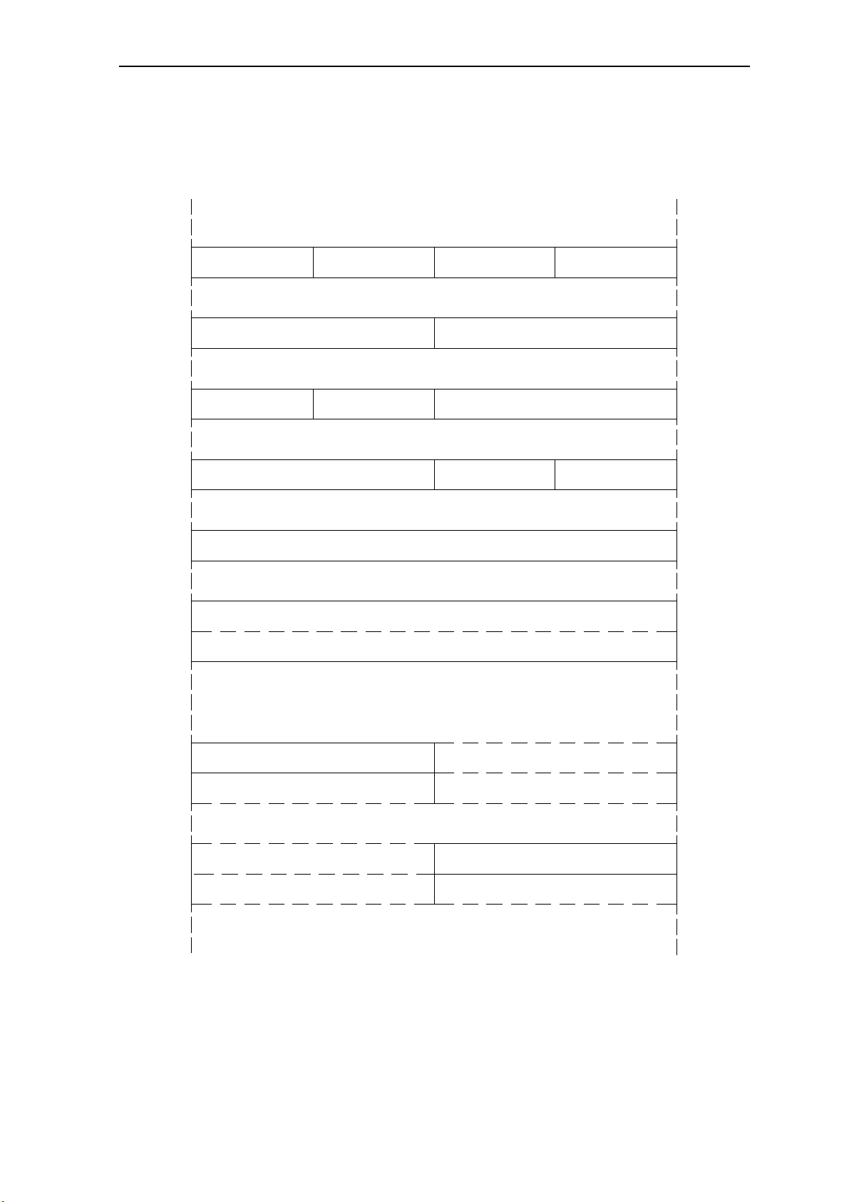
Figure 1.9 shows the creation and release of stack frames in the register part of the stack.
Return from B Call B Frame in B
PC := ret. PC for B; PC := branch address; FP := FP - code of source reg.;
SR := ret. SR for B; ret. PC for B := old PC; FL := code of dest.reg.;
-- returns preceding stack frame ret. SR for B := old SR; if available registers ≥
if stack frame contained FP := FP + reg.code (required + 10) registers then
in local registers then of ret. PC; next instruction
next instruction; FL := 6; else
else -- reg.code of ret. PC = 9 push contents of
pull contents of differential words differential number of
from memory part of the stack; registers to memory
part of stack;
-- code of source reg. = 2
-- code of dest.reg. = 11
Frame
Pointer
(FP)
FP+FL
parameters
for
frame A frame A frame A
ret. PC for A
ret. SR for A
reserved
for
maximum
number of
variables
in frame A
L0
L1
L2
L3
L4
L5
L6
L7
L8
L9
L10
L11
L12
L13
L14
L15
current
length
of
frame A
FL = 13
New
FP
must not
be used
FP+FL
parameters
for
ret. PC for A
ret. SR for A
parameters
for frame B
ret. PC for B
ret. SR for B
reserved for
max. number
of variables
in frame B
L0
L1
L2
L3
L4
L5
current
length
of
frame B
FL = 6
New
FP
FP+FL
parameters
ret. PC for A
ret. SR for A
parameters
for frame B
ret. PC for B
ret. SR for B
reserved
maximum
number of
variables
in frame B
for
for
L0
L1
L2
L3
L4
L5
L6
L7
L8
L9
L10
current
length
of
frame B
FL = 11
before Call and after CALL L9, 0, dest; after FRAME L11, L2
after Return
Figure 1.9: Stack frame handling (register part)

Page 1-24 Architecture
before Frame Instruction for frame X after Frame Instruction for frame X
register part
of the stack
overlap modulo 64
A
rest of frame A
FP
available for X
space for X
X
A and X
words
to be
pushed
various
frames
space
additional
required
memory part
of the stack
stack
space
required
pushed number
of words
according to
space required
for frame X
SP
FP
register part
of the stack
rest of frame A
various
frames
additional
space for X
available
memory part
of the stack
stack
space
appended
SP
FP
before Return Instruction to frame A after Return Instruction to frame A
words for A
A
rest of frame A
X
overwritten
frame
required
various
frames
words
to be
= available part of a frame
words
to be
pulled
pulled number
of words
completes
stack frame A!
SP
A
rest of frame A
frame
words
pulled
various
frames
stack
space
freed
SPFP
Figure 1.10: Stack frame pushing and popping

E1-32XS User’s Manual Page 1-25
1.9. Instruction Cache
The instruction cache is transparent to programs. A program executes correctly even if it
ignores the cache, whereby it is assumed that a program does not modify the instruction
code in the local range contained in the cache.
The instruction cache holds a total of up to 128 bytes (32 unstructured 32-bit words of
instructions). It is implemented as a circular buffer which is guarded by a look-ahead
counter and a look-back counter. The look-ahead counter holds the highest and the lookback counter the lowest address of the instruction words available in the cache. The cachemode flag M is used to optimize special cases in loops (see details below). The cache can
be regarded as a temporary local window into the instruction sequence, moving along with
instruction execution and being halted by the execution of a program loop.
Its function is as follows:
The prefetch control loads unstructured 32-bit instruction words (without regard to instruction boundaries) from memory into the cache. The load operation is pipelined to a depth of
two stages (see section 3.1. Memory Instructions for details of the load pipeline). The
look-ahead counter is incremented by four at each prefetch cycle. It always contains the
address of the last instruction word for which an address bus cycle is initiated, regardless
of whether the addressed instruction word is in the load pipeline or already loaded into the
instruction cache.
The prefetched instruction word is placed in the cache word location addressed by bits 6..2
of the look-ahead counter. The look-back counter remains unchanged during prefetch
unless the cache word location it addresses with its bits 6..2 is overwritten by a prefetched
instruction word. In this case, it is incremented by four to point to the then lowestaddressed usable instruction word in the cache. Since the cache is implemented as a
circular buffer, the cache word addresses derived from bits 6..2 of the look-ahead and lookback counter wrap around modulo 32.
The prefetch is halted:
❒ When eight words are prefetched, that is, eight words are available (including those
pending in the load pipeline) in the prefetch sequence succeeding the instruction word
addressed by the program counter PC through the instruction word addressed by the
look-ahead counter. Prefetch is resumed when the PC is advanced by instruction
execution.
❒ In the cycle preceding the execution cycle of an instruction accessing memory or I/O or
any potentially branch-causing instruction (regardless of whether the branch is taken)
except a forward Branch or Delayed Branch instruction with an instruction length of
one half-word and a branch target contained in the cache. Halting the prefetch in these
cases avoids filling the load pipeline with demands for potentially unnecessary
instruction words. The prefetch is also halted during the execution cycle of any
instruction accessing memory or I/O.

Page 1-26 Architecture
The cache is read in the decode cycle by using bits 6..1 of the PC as an address to the first
half-word of the instruction presently being decoded. The instruction decode needs and
uses only the number (1, 2 or 3) of instruction half-words defined by the instruction
format. Since only the bits 6..1 of the PC are used for addressing, the half-word addresses
wrap around modulo 64. Idle wait cycles are inserted when the instruction is not or not
fully available in the cache.
At an explicit Branch or Delayed Branch instruction (except when placed as delay
instruction) with an instruction length of one half-word, the location of the branch target is
checked. The branch target is treated as being in the cache when the target address of a
backward branch is not lower than the address in the look-back counter and the target
address of a forward branch is not higher than two words above the address in the lookahead counter. That is, the two instruction words succeeding the instruction word
addressed by the content of the look-ahead counter are treated by a forward branch as
being in the cache. Their actual fetch overlaps in most cases with the execution of the
branch instruction and thus, no cycles are wasted. When the branch target is in the cache,
the look-back counter and the look-ahead counter remain unchanged.
When a branch is taken by a Delayed Branch instruction with an instruction length of one
half-word to a forward branch target not in the cache and the cache mode flag M is enabled
(1), the look-back counter and the look-ahead counter remain unchanged. Wait cycles are
then inserted until the ongoing prefetch has loaded the branch target instruction into the
cache.
Any other branch taken flushes the cache by placing the branch address in the look-back
and the look-ahead counter. Prefetch then starts immediately at the branch address.
Instruction decoding waits until the branch target instruction is fully available in the cache.
The cache mode flag M (bit four of the SR) can be set or cleared by logical instructions. It
is automatically cleared by a Frame instruction and by any branch taken except a branch
caused by a Delayed Branch or Return instruction; a Delayed Branch instruction leaves the
M flag unchanged and a Return instruction restores the M flag from the saved status
register SR.
Note: Since up to eight instruction words can be loaded into the cache by the prefetch, only
24 instruction words are left to be contained in a program loop. Thus, a program loop can
have a maximum length of 96 or 94 bytes including the branch instruction closing the loop,
depending on the even or odd half-word address location of the first instruction of the loop
respectively.
A forward Branch or Delayed Branch instruction with an instruction length of one halfword into up to two instruction words succeeding the word addressed by the look-ahead
counter treats the branch target as being in the cache and does not flush the cache. Thus,
three or four instruction half-words, depending on the odd or even half-word address
location of the branch instruction respectively, can always be skipped without flushing the
cache.

E1-32XS User’s Manual Page 1-27
Enabling the cache-mode flag M is only required when a program loop to be contained in
the cache contains a forward branch to a branch target in the program loop and more than
three (or four, see above) instruction half-words are to be skipped. In this case, the enabled
M flag in combination with a Delayed Branch instruction with an instruction length of one
half-word inhibits flushing the cache when the branch target is not yet prefetched.
Since a single-word memory instruction halts the prefetch for two cycles, any sequence of
memory instructions, even with interspersed one-cycle non-memory instructions, halts the
prefetch during its execution. Thus, alternating between instruction and data memory
pages is avoided. If the number of instruction half-words required by such a sequence is
not guaranteed to be in the cache at the beginning of the sequence, a Fetch instruction
enforcing the prefetch of the sequence may be used. A Fetch instruction may also be used
preceding a branch into a program loop; thus, flushing the cache by the first branch
repeating the loop can be avoided.
A branch taken caused by a Branch or Delayed Branch instruction with an instruction
length of two half-words always flushes the instruction cache, even if the branch target is
in the cache. Thus, branches can be forced to bypass the cache, thereby reducing the cache
to a prefetch buffer. This reduced function can be used for testing.
1.10. On-Chip Memory (IRAM)
16 KBytes of memory are provided on-chip. The on-chip memory (IRAM) is mapped to
the hex address C000 0000 of the memory address space and wraps around modulo 16K up
to DFFF FFFF. The IRAM is implemented as a fully static memory block.
An access to the IRAM bypasses the access pipeline of the external memory. Thus, pending external memory accesses do not delay accesses to the IRAM. The IRAM can hold
data as well as instructions. Instruction words from the IRAM are automatically transferred
to the instruction cache on demand; these transfers do not interfere with external memory
accesses. Besides bypassing of the external memory pipeline, memory instructions accessing the IRAM behave exactly alike those accessing external memory. The minimum delay
for a load access is one cycle; that is, the data is not available in the cycle after the load
instruction. One or more wait cycles are automatically inserted if the target register of the
load is addressed before the data is loaded into the target register.
Attention: For selection between an internal and external memory access, bits 31..29 of the
specified address register are used before calculation of the effective address. Therefore,
the content of the specified address register must point into the IRAM address range. The
IRAM address range boundary must not be crossed when the effective memory address is
calculated in the displacement address mode.


E1-32XS User’s manual Page 2-1
2. Instructions General
2.1. Instruction Notation
In the following instruction-set presentation, an informal description of an instruction is
followed by a formal description in the form:
Format Notation Operation
Format denotes the instruction format.
Notation gives the assembler notation of the instruction.
Operation describes the operation with the following symbols:
Ls denotes any of the local registers L0..L15 used as source register or as source
operand. At memory Load instructions, Ls denotes the load destination register.
Ld denotes any of the local registers L0..L15 used as destination register or as
destination operand.
Rs denotes any of the local registers L0..L15 or any of the global registers G0..G15
used as source register or as source operand. At memory Load instructions, Rs
denotes the load destination register.
Rd denotes any of the local registers L0..L15 or any of the global registers G0..G15
used as destination register or as destination operand.
Lsf, Ldf, Rsf and Rdf denote the register or operand following after (with a register address
one higher than) Ls, Ld, Rs and Rd respectively.
imm, const, dis, lim, rel, adr and n denote immediate operands (constants) of various
formats and ranges.
Operand(x) denotes a single bit at the bit position x of an operand.
Example: Ld(31) denotes bit 31 of Ld.
Operand(x..y) denotes bits x through y of an operand.
Example: Ls(4..0) denotes bits 4 through 0 of Ls.
Expression^ denotes an operand at a location addressed by the value of the expression.
Depending on the context, the expression addresses a memory location or a local
register.
Example: Ld^ denotes a memory operand whose memory address is the operand
Ld. (FP + FL)^ denotes a local register operand whose register address is FP + FL.
:= signifies the assignment symbol, read as "is replaced by".
// signifies the concatenation symbol. It denotes concatenation of two operand words
to a double-word operand or concatenation of bits and bitstrings.
Examples: Ld//Ldf denotes a double-word operand, 16 zeros//imm1 denotes
expanding of an immediate half-word by 16 leading zeros.
=, ≠, > and < denote the equal, unequal, greater than and less than relations.
Example: The relation Ld = 0 evaluates to one if Ld is equal to zero, otherwise it
evaluates to zero.

Page 2-2 Instructions General
2.2. Instruction Execution
On instruction execution, all bits of the operands participate in the operations, except on
the Shift and Rotate instructions (whereat only the 5 least significant bits of the source
operand are used) and except on the byte and half-word Store instructions.
Instructions are executed by a two-stage pipeline. In the first stage, the instruction is
fetched from the instruction cache and decoded. In the second stage, the instruction is
executed while the next instruction in the first stage is already decoded.
On register instructions executing in one or two cycles, the corresponding source and
destination operand words are read from their registers and evaluated in each cycle in
which they are used. Then the result word is placed in the corresponding destination
register in the same cycle. Thus, on all single-word register instructions executing in one
cycle, the source operand register and the destination operand register may coincide
without changing the effect of the instruction. On all other instructions, the effect of a
register coincidence depends on execution order and must be examined specifically for
each such instruction.
The content of a source register remains unchanged unless it is used coincidentally as a
destination register (except on memory Load instructions).
Some instructions set or clear condition flags according to the result and special conditions
occuring during their execution. The conditions may be expressed by single bits, relations
or logical combinations of these. If a condition evaluates to one (true), the corresponding
condition flag is set to one, if it evaluates to zero (false), the corresponding condition flag
is cleared to zero. If the conditions for a Range Error are met, a trap to Range Error occurs
after the flags and the destination are updated.
All instructions may use the result and any flags updated by the preceding instruction. A
time penalty occurs only if the result of a memory Load instruction is not yet available
when needed as destination or source operand. In this case one or more (depending on the
memory access time) idle wait cycles are enforced by a hardware interlock.
An instruction must not use any local register of the register sequence beginning with L0
beyond the number of usable registers specified by the current value of the frame length
FL (FL = 0 is interpreted as FL = 16). That is, the value of the corresponding register code
(0..15) addressing a local register must be lower than the interpreted value of the FL
(except with a Call or Frame instruction or some restricted cases). Otherwise, an exception
could overwrite the contents of such a register or the beginning of the register part of the
stack at the SP could be overwritten without any warning when a result is placed in such a
register.
Double-word instructions denote the high-order word (at the lower address). The low-order
word adjacently following it (at the higher address) is implied.
"Old" denotes the state before the execution of an instruction.

E1-32XS User’s manual Page 2-3
2.3. Instruction Formats
Instructions have a length of one, two or three half-words and must be located on halfword boundaries. The following formats are provided:
Format
15 87 43 0
LL
LLext OP-code
LR
RR
Ln
OP-code Ld-code Ls-code
15 8
OP-code s Ld-code Rs-code
OP-Code d s Rd-code Rs-code
OP-code n Ld-code n
Configuration
7430
Ld-code Ls-code
OP-code extension
915 87 43 0
10 915 87 43 0
915 87 43 0
s = 0:
s = 1:
s = 0:
s = 1:
d = 0:
d = 1:
n:
Ls-code encodes L0..L15 for Ls
Ld-code encodes L0..L15 for Ld
Ls-code encodes L0..L15 for Ls
Ld-code encodes L0..L15 for Ld
OP-code extension encodes the
EXTEND instructions
Rs-code encodes G0..G15 for Rs
Rs-code encodes L0..L15 for Rs
Ld-code encosed L0..L15 for Ld
Rs-code encodes G0..G15 for Rs
Rs-code encodes L0..L15 for Rs
Rd-code encodes G0..G15 for Rd
Rd-code encodes L0..L15 for Rd
Ld-code encodes L0..L15 for Ld
Bit 8//bits 3..0 encode n = 0..31
10 915 87 43 0
Rn
PCadr
PCrel
PCrel
OP-Code d n Rd-code n
15 8 7 0
OP-code adr-byte
15 8 7 061
OP-code 0 low-rel S
15 8 7 061
OP-code 1 high-rel
low-rel S
Table 2.1: Instruction Formats, Part 1
d = 0:
d = 1:
n:
S:
S:
Rd-code encodes G0..G15 for Rd
Rd-code encodes L0..L15 for Rd
Bit 8//bits 3..0 encode n = 0..31
adr = 24 ones's//adr-byte(7..2)//00
sign bit of rel
rel = 25 S//low-rel//0
range -128..126
sign bit of rel
rel = 9 S//high-rel//low-rel//0
range -8 388 608..8 388 606

Page 2-4 Instructions General
2
2
Format
LRconst
RRconst
RRdis
Configuration
14
OP-code s Ld-code Rs-code
e S const1
14
OP-code s Rd-code Rs-code
e const1
14
OP-code s Rd-code Rs-code
eSSD D dis1
915 8 7 4 3 0 Rs-code encodes G0..G15 for Rs
const2
10 915 8 7 4 3 0
d
const2
10 915 8 7 4 3 0
d
dis2
s = 0:
s = 1:
S:
e = 0:
e = 1:
s = 0:
s = 1:
d = 0:
d = 1:
S:
e = 0:
e = 1:
s = 0:
s = 1:
d = 0:
d = 1:
S:
e = 0:
e = 1:
DD:
Rs-code encodes L0..L15 for Rs
Ld-code encodes L0..L15 for Ld
Sign bit of const
const = 18 S//const1
range -16 384..16 383
const = 2 S//const1//const2
range -1 073 741 824..1 073 741 8
Rs-code encodes G0..G15 for Rs
Rs-code encodes L0..L15 for Rs
Rd-code encodes G0..G15 for Rd
Rd-code encodes L0..L15 for Rd
Sign bit of const
const = 18 S//const 1
range -16 384..16 383
const = 2 S//const1//const2
range -1 073 741 824..1 073 741 8
Rs-code encodes G0..G15 for Rs
Rs-code encodes L0..L15 for Rs
Rd-code encodes G0..G15 for Rd
Rd-code encodes L0..L15 for Rd
Sign bit of dis
dis = 20 S//dis1
range -4 096..4 095
dis = 4 S//dis1//dis2
range -268 435 456..268 435 455
D-code, D13..D12 encode data
types at memory instructions
10 915 8 7 4 3 0
Rimm
RRlim
OP-code n Rd-code n
14
OP-code s Rd-code Rs-code
e X X X lim1
d
imm1
imm2
10 915 8 7 4 3 0
d
lim2
Table 2.2: Instruction Formats, Part 2
d = 0:
d = 1:
n:
s = 0:
s = 1:
d = 0:
d = 1:
XXX:
e = 0:
e = 1:
Rd-code encodes G0..G15 for Rd
Rd-code encodes L0..L15 for Rd
Bit 8//bits 3..0 encode n = 0..31
see Table 2.3. Encoding of
Immediate Values for encoding of
imm
Rs-code encodes G0..G15 for Rs
Rs-code encodes L0..L15 for Rs
Rd-code encodes G0..G15 for Rd
Rd-code encodes L0..L15 for Rd
X-code, X14..X12 encode Index
instructions
lim = 20 zeros//lim1
range 0..4 095
lim = 4 zeros//lim1//lim2
range 0..268 435 455

E1-32XS User’s manual Page 2-5
2.3.1. Table of Immediate Values
n immediate value imm Comment
0..16 0..16 at CMPBI, n = 0 encodes ANYBZ
at ADDI and ADDSI n = 0 encodes CZ
17 imm1//imm2 range = 0..232-1 or -231..231-1
18 16 zeros//imm1 range = 0..65 535
19 16 ones//imm1 range = -65 536..-1
20 32 bit 5 = 1, all other bits = 0
21 64 bit 6 = 1, all other bits = 0
22 128 bit 7 = 1, all other bits = 0
23 231 bit 31 = 1, all other bits = 0
24 -8
25 -7
26 -6
27 -5
28 -4
29 -3
30 -2
31 231-1 at CMPBI and ANDNI
bit 31 = 0, all other bits = 1
31 -1 at all other instructions using imm
Table 2.3: Encoding of Immediate Values
Note: 231 provides clear, set and invert of the floating-point sign bit at ANDNI, ORI and
XORI respectively.
31
2
-1 provides a test for floating-point zero at CMPBI and extraction of the sign bit at
ANDNI.
See CMPBI for ANYBZ and ADDI, ADDSI for CZ.

Page 2-6 Instructions General
2.3.2. Table of Instruction Codes
CALL
EXTEND DO
DIV S
SUMS
SUM
DIV U
XOR
OR
SUBS
SUB
NEGS
NEG
ADDS
ADD
XORI
ADDSI
ORI
ADDI
STxx.N/S
RESERVED TESTLZ ROL
MUL
RESERVED
FCVTDFCVT
STW.P STD. P
FCMPU FCMPUD
SHLI
TRAPxx, TRAP
FRAMEDBR
BR
BGT
DBGT
BLE
DBLE
BNNBN
STxx .D/ A/ IOD/ IOA
SHL DI SHL D SHL
FCMPDFCMP
SETxx, SETADR, FETCH
DBNNDBN
STW.R STD.R
BHT
DBHT
OP-code Bits 11..8
FDIV FDIVD
NOT
MOV
MASK
MOVD, RET
ANDN
AND
MOV I
ANDNI
SARDI SARD SAR
SARI
LDxx.N/S
MUL S
FMULDFMUL
LDW. P LDD.P
23106754AB98DCFE
FSUB FSUBD
DBSE
DBNCDBC
DBNE
DBE
BSE
BNCBC
BNE
BE
CMP
XMx, XXx
CHK, CHKZ, NOP
SUBC
CMPB
OP-code Bits 15..12
0
1
2
3
4
Table 2.4: Table of Instruction Codes
CMPI
ADDC
5
CMPBI
SHRDI SHRD SHR
6
7
8
SHRI
MUL U
BNVBV
LDxx .D/ A/ IOD/ IOA
9
A
FADDDFADD
B
C
DBNVDBV
LDW. R LDD. R
F
E
D

E1-32XS User’s manual Page 2-7
2.3.3. Table of Extended DSP Instruction Codes
The Extended DSP instructions are specified by a 16-bit OP-code extension succeeding the
instruction op-code for the EXTEND instruction. See section 3.32. Extended DSP
Instructions.
Instruction OP-code
extension (hex)
EMUL 0102
EMULU 0104
EMULS 0106
EMAC 010A
EMACD 010E
EMSUB 011A
EMSUBD 011E
EHMAC 002A
EHMACD 002E
EHCMULD 0046
EHCMACD 004E
EHCSUMD 0086
EHCFFTD 0096
EHCFFTSD 0296
Table 2.5: Extended DSP Instruction Codes

Page 2-8 Instructions General
2.4. Entry Tables
Spacing of the entries for the Trap instructions and exceptions is four bytes. These entries
are intended to each contain an instruction branching to the associated function. The
entries for the TRAPxx instructions are the same as for TRAP. Table 2.6 shows the trap
entries when the entry table is mapped to the end of memory area MEM3 (default after
Reset):
Address (Hex) Entry Description
FFFF FF00 TRAP 0
FFFF FF04 TRAP 1
: :
FFFF FFC0 TRAP 48 IO2 Interrupt -- priority 15
FFFF FFC4 TRAP 49 IO1 Interrupt -- priority 14
FFFF FFC8 TRAP 50 INT4 Interrupt -- priority 13
FFFF FFCC TRAP 51 INT3 Interrupt -- priority 11
FFFF FFD0 TRAP 52 INT2 Interrupt -- priority 9
FFFF FFD4 TRAP 53 INT1 Interrupt -- priority 7
FFFF FFD8 TRAP 54 IO3 Interrupt -- priority 5
FFFF FFDC TRAP 55 Timer Interrupt -- priority selectable as 6, 8, 10, 12
FFFF FFE0 TRAP 56 Reserved -- priority 17 (lowest)
FFFF FFE4 TRAP 57 Trace Exception -- priority 16
FFFF FFE8 TRAP 58 Parity Error -- priority 4
FFFF FFEC TRAP 59 Extended Overflow -- priority 3
FFFF FFF0 TRAP 60 Range, Pointer, Frame and Privilege Error -- priority 2
FFFF FFF4 TRAP 61 Reserved -- priority 1
FFFF FFF8 TRAP 62 Reset -- priority 0 (highest)
FFFF FFFC TRAP 63 Error entry for instruction code of all ones
Table 2.6: Trap entry table mapped to the end of MEM3

E1-32XS User’s manual Page 2-9
Table 2.7 shows the trap entries when the entry table is mapped to the beginning of
memory areas MEM0, MEM1, MEM2 or IRAM. x is 0, 4, 8 or C corresponding to the
mapping to MEM0, MEM1, MEM2 or IRAM respectively.
Address (Hex) Entry Description
x000 0000 TRAP 63 Error entry for instruction code of all ones
x000 0004 TRAP 62 Reserved -- priority 0 (highest)
x000 0008 TRAP 61 Reserved -- priority 1
x000 000C TRAP 60 Range, Pointer, Frame and Privilege Error -- priority 2
x000 0010 TRAP 59 Extended Overflow -- priority 3
x000 0014 TRAP 58 Parity Error -- priority 4
x000 0018 TRAP 57 Trace Exception -- priority 16
x000 001C TRAP 56 Reserved -- priority 17 (lowest)
x000 0020 TRAP 55 Timer Interrupt -- priority selectable as 6, 8, 10, 12
x000 0024 TRAP 54 IO3 Interrupt -- priority 5
x000 0028 TRAP 53 INT1 Interrupt -- priority 7
x000 002C TRAP 52 INT2 Interrupt -- priority 9
x000 0030 TRAP 51 INT3 Interrupt -- priority 11
x000 0034 TRAP 50 INT4 Interrupt -- priority 13
x000 0038 TRAP 49 IO1 Interrupt -- priority 14
x000 003C TRAP 48 IO2 Interrupt -- priority 15
: :
x000 00F8 TRAP 1
x000 00FC TRAP 0
Table 2.7: Trap entry table mapped to the beginning of MEM0, MEM1, MEM2 or IRAM

Page 2-10 Instructions General
Table 2.8 below shows the addresses of the first instruction of the emulator code
associated with the floating-point instructions when the trap entry tables are mapped to the
end of memory area MEM3. Spacing of the entries for the Software instructions
FADD..DO is 16 bytes.
Address (Hex) Entry Description
FFFF FE00 FADD Floating-point Add, single word
FFFF FE10 FADDD Floating-point Add, double-word
FFFF FE20 FSUB Floating-point Subtract, single word
FFFF FE30 FSUBD Floating-point Subtract, double-word
FFFF FE40 FMUL Floating-point Multiply, single word
FFFF FE50 FMULD Floating-point Multiply, double-word
FFFF FE60 FDIV Floating-point Divide, single word
FFFF FE70 FDIVD Floating-point Divide, double-word
FFFF FE80 FCMP Floating-point Compare, single word
FFFF FE90 FCMPD Floating-point Compare, double-word
FFFF FEA0 FCMPU Floating-point Compare Unordered, single word
FFFF FEB0 FCMPUD Floating-point Compare Unordered, double-word
FFFF FEC0 FCVT
FFFF FED0 FCVTD
FFFF FEE0 Reserved
FFFF FEF0 DO Do instruction
Table 2.8: Floating-Point entry table mapped to the end of MEM3
Floating-point Convert single word ⇒ double-word
Floating-point Convert double-word ⇒ single word

E1-32XS User’s manual Page 2-11
Table 2.9 below shows the addresses of the first instruction of the emulator code
associated with the floating-point instructions when the trap entry tables are mapped to the
beginning of memory areas MEM0, MEM1, MEM2 or IRAM. x is 0, 4, 8 or C
corresponding to the mapping to MEM0, MEM1, MEM2 or IRAM respectively.
Address (Hex) Entry Description
x000 010C DO Do instruction
x000 011C Reserved
x000 012C FCVTD
x000 013C FCVT
x000 014C FCMPUD Floating-point Compare Unordered, double-word
x000 015C FCMPU Floating-point Compare Unordered, single word
x000 016C FCMPD Floating-point Compare, double-word
x000 017C FCMP Floating-point Compare, single word
x000 018C FDIVD Floating-point Divide, double-word
x000 019C FDIV Floating-point Divide, single word
x000 01AC FMULD Floating-point Multiply, double-word
x000 01BC FMUL Floating-point Multiply, single word
x000 01CC FSUBD Floating-point Subtract, double-word
x000 01DC FSUB Floating-point Subtract, single word
x000 01EC FADDD Floating-point Add, double-word
x000 01FC FADD Floating-point Add, single word
Table 2.9: Floating-Point entry table mapped to the beginning of MEM0, MEM1, MEM2 or IRAM
Floating-point Convert double-word ⇒ single word
Floating-point Convert single word ⇒ double-word

Page 2-12 Instructions General
2.5. Instruction Timing
The following execution times are given in number of processor clock cycles.
All instructions not shown below: 1 cycle
Move double-word: 2 cycles
Shift double-word: 2 cycles
Test Leading Zeros: 2 cycles
Multiply word:
when both operands are in the range of -2
15
..215-1: 3 cycles
all other cases: 5 cycles
Multiply double-word signed:
when both operands are in the range of -2
15
..215-1: 4 cycles
all other cases: 6 cycles
Multiply double-word unsigned:
when both operands are in the range of 0..2
16
-1: 4 cycles
all other cases: 6 cycles
Divide unsigned and signed: 36 cycles
Branch instructions when branch not taken: 1 cycle
when branch taken and target in on-chip cache: 2 cycles
when branch taken and target in memory : 2 + memory read latency cycles
(see next page)
Delayed Branch instructions when branch not taken: 1 cycle
when branch taken and target in on-chip cache: 1 cycle
when branch taken and target in memory: 1 + memory read latency cycles exceeding
(delay instruction cycles - 1)
Call and Trap instructions when branch not taken: 1 cycle
when branch taken: 2 + memory read latency cycles
Software instructions: 6 + memory read latency cycles exceeding 4 cycles
Frame when not pushing words on the stack: 3 cycles
additionally when pushing n words on the stack: memory write latency cycles
+ n * bus cycles per access
-- write latency = cycles elapsed until write access cycle of first word stored
(minimum = 1 at a non-RAS access and no pipeline congestion)
Return:
4 + memory read latency cycles exceeding 2 cycles
additionally when pulling n words from the stack: memory RAS latency
+ n * bus cycles per access
(RAS latency applies only at n > 2, otherwise RAS latency is always 0)
-- RAS latency = RAS precharge cycles + RAS to CAS delay cycles

E1-32XS User’s manual Page 2-13
Fetch instruction:
when the required number of instruction half-words are already prefetched in the
instruction cache: 1 cycle
otherwise
1 + (required number of half-words - number of half-words already prefetched)/2
* bus cycles per access
Memory word instructions, non-stack address mode:
1 cycle
Memory word instructions, stack address mode:
3 cycles
Memory double-word instructions:
2 cycles
For timing calculations, double-word memory instructions are treated like a sequence of
two single-word memory instructions.
Idle wait cycles are transparently inserted when a memory instruction has to wait for
execution because the two-stage address pipeline is full.
Instruction execution proceeds after the execution of a Load instruction until the data
requested is needed (that is, the register into which the data is to be loaded is addressed) by
a further instruction.
The cycles executed between the memory instruction cycle requesting the data and the first
cycle at which the data are available are called read latency cycles. These read latency
cycles can be filled with instructions which do not need the requested data. When, after the
execution of these optional fill instruction cycles, the data is still not available in the cycle
needing it, idle wait cycles are inserted until the data is available. The idle wait cycles are
inserted transparently to the program by an on-chip hardware interlock. The read latency
is:
On an IRAM access:
read latency = 1 cycle
On a non-RAS external memory or I/O access:
read latency = address setup cycles + access cycles + 1
On a RAS memory access:
read latency = RAS precharge cycles + RAS to CAS delay cycles +
access cycles + 1
Additional cycles are also inserted and add to the latency when the address pipeline is
congested, these cycles must then also be taken into calculation.
A switch from an external memory or I/O read access to an immediately succeeding write
access inserts one additional bus cycle.
Extended DSP instructions:
The instruction issue time is always 1 cycle. After the issue of an Extended DSP
instruction, execution of non-Extended-DSP instructions proceeds while the Extended DSP
instruction is executed in the multiply/accumulate unit.

Page 2-14 Instructions General
Latency cycles are defined as the time that the multiply-accumulate execution unit is busy
executing the Extended DSP instruction. In the last latency cycle of an Extended DSP
instruction that is currently executed, the issue cycle of the next Extended DSP instruction
may take place. An Extended DSP instruction succeeding a currently running Extended
DSP instruction after less than the latency cycles for the running instructions is delayed
until the last latency cycle of the running instruction is reached.
One additional latency cycle passes until the instruction result is available in the register
G15 or register pair G14//G15 to an ALU instruction referencing that result. Any
instruction referencing the Extended DSP instruction result earlier is delayed until the
result is available in G15 or G14//G15.
The latency cycles are as follows:
EMUL instruction:
when both operands are in the range of -2
15
..215-1: 1 cycle
all other cases: 3 cycles
EMULU instruction:
when both operands are in the range of 0..2
16
-1: 1 cycle
all other cases: 4 cycles
EMULS instruction:
when both operands are in the range of -2
all other cases: 4 cycles
EMAC instruction:
when both operands are in the range of -2
all other cases: 3 cycles
EMACD instruction:
when both operands are in the range of -2
all other cases: 4 cycles
EMSUB instruction:
when both operands are in the range of -2
all other cases: 3 cycles
EMSUBD instruction:
when both operands are in the range of -2
all other cases: 4 cycles
EHMAC, EHMACD instructions: 2 cycles
EHCMULD, EHCMACD instructions: 4 cycles
EHCSUMD instruction: 1 cycles
15
..215-1: 1 cycle
15
..215-1: 1 cycle
15
..215-1: 1 cycle
15
..215-1: 1 cycle
15
..215-1: 1 cycle
EHCFFTD, EHCFFTSD instructions: 1 cycles
Thus, after issue of for example a EHCMULD instruction, there are three clock cycles
available for the issue of ALU instructions until the next Extended DSP instruction can be
issued, and the result of the EHCMULD instruction is available in G14//G15 five clock
cycles after instruction issue.

E1-32XS User’s manual Page 3-1
3. Instruction Set
3.1. Memory Instructions
The memory instructions load data from memory in a register Rs (or a register pair
Rs//Rsf) or store data from Rs (or Rs//Rsf) to memory using the data types byte
unsigned/signed, half-word unsigned/signed, word or double-word. Since I/O devices are
also addressed by memory instructions, "memory" stands here interchangeably also for I/O
unless memory or I/O address space is specifically denoted.
The memory address is either specified by the operand Rd or Ld, by the sum Rd plus a
signed displacement or by the displacement alone, depending on the address mode.
Memory accesses to words and double-words ignore bits one and zero of the address,
memory accesses to half-words ignore bit zero of the address, (since these operands are
located at word or half-word boundaries respectively, these address bits are redundant).
If the content of any register Rd except SR is zero, the memory is not accessed and a trap
to Pointer Error occurs (see section 4. Exceptions). Thus, uninitialized pointers are
automatically checked.
Load and Store instructions are pipelined to a total depth of two word entries for Load and
Store, thus, a double-word Load or a double-word Store instruction can be executed
without halting the processor in a wait state. (The address pipeline provides a depth of two
addresses common to load and store).
Double-word memory instructions insert two separate word and address entries into the
pipeline and start two independent memory cycles. The first memory cycle, loading or
storing the high-order word, uses the address specified by the address mode, the second
cycle uses this address incremented by four and also places it on the address bus.
Accessing data in the same DRAM memory page by any number of succeeding memory
cycles is performed in page mode.
Memory instructions leave all condition flags unchanged.

Page 3-2 Instruction Set
3.1.1. Address Modes
3.1.1.1. Register Address Mode:
Notation: LDxx.R, STxx.R -- xx: word or double-word data type
The content of the destination register Ld is used as an address into memory address space.
3.1.1.2. Postincrement Address Mode:
Notation: LDxx.P, STxx.P -- xx: word or double-word data type
The content of the destination register Ld is used as an address into memory address space,
then Ld is incremented according to the specified data size of a word or double-word
memory instruction by 4 or 8 respectively, regardless of any exception occuring. In the
case of a double-word data type, Ld is incremented by 8 at the first memory cycle.
3.1.1.3. Displacement Address Mode:
Notation: LDxx.D, STxx.D -- xx: any data type
The sum of the contents of the destination register Rd plus a signed displacement dis is
used as an address into memory address space.
Rd may denote any register except the SR; Rd not denoting the SR differentiates this mode
from the absolute address mode.
In the case of all data types except byte, bit zero of dis is treated as zero for the calculation
of Rd + dis.
Note: Specification of the PC for Rd provides addressing relative to the address of the first
byte after the memory instruction.
3.1.1.4. Absolute Address Mode:
Notation: LDxx.A, STxx.A -- xx: any data type
The displacement dis is used as an address into memory address space. Rd must denote the
SR to differentiate this mode from the displacement address mode; the content of the SR is
not used.
In the case of all data types except byte, address bit zero is supplied as zero.
Note: The displacement provides absolute addressing at the beginning and the end (MEM3
area) of the memory.

E1-32XS User’s manual Page 3-3
3.1.1.5. I/O Displacement Address Mode:
Notation: LDxx.IOD, STxx.IOD -- xx: word or double-word data type
The sum of the contents of the destination register Rd plus a signed displacement dis is
used as an address into I/O address space.
Rd may denote any register except the SR; Rd not denoting the SR differentiates this mode
from the I/O absolute address mode.
Bits one and zero of dis are treated as zero for the calculation of Rd + dis.
Execution of a memory instruction with I/O displacement address mode does not disrupt
any page mode sequence.
Note: The I/O displacement address mode provides dynamic addressing of peripheral
devices.
When on a load instruction only a byte or half-word is placed on the (lower part) of the
data bus, the higher-order bits are undefined and must be masked out before the loaded
operand is used further.
3.1.1.6. I/O Absolute Address Mode:
Notation: LDxx.IOA, STxx.IOA -- xx: word or double-word data type
The displacement dis is used as an address into I/O address space.
Rd must denote the SR to differentiate this mode from the I/O displacement address mode;
the content of the SR is not used.
Address bits one and zero are supplied as zero.
Execution of a memory instruction with I/O address mode does not disrupt any page mode
sequence.
Note: The I/O absolute address mode provides code efficient absolute addressing of
peripheral devices and allows simple decoding of I/O addresses.
When on a load instruction only a byte or a half-word is placed on the (lower part) of the
data bus, the higher-order bits are undefined and must be masked out before the loaded
operand is used further.

Page 3-4 Instruction Set
3.1.1.7. Next Address Mode:
Notation: LDxx.N, STxx.N -- xx: any data type
The content of the destination register Rd is used as an address into memory address space,
then Rd is incremented by the signed displacement dis regardless of any exception
occurring. At a double-word data type, Rd is incremented at the first memory cycle.
Rd must not denote the PC or the SR.
In the case of all data types except byte, bit zero of dis is treated as zero for the calculation
of Rd + dis.
3.1.1.8. Stack Address Mode:
Notation: LDW.S, STW.S -- only word data type
The content of the destination register Rd is used as stack address, then Rd is incremented
by dis regardless of any exception occurred.
A stack address addresses memory address space if it is lower than the stack pointer SP;
otherwise bits 7..2 of it (higher bits are ignored) address a register in the register part of the
stack absolutely (not relative to the frame pointer FP).
Bits one and zero of dis are treated as zero for the calculation of Rd + dis.
Rd must not denote the PC or the SR.
Note: The stack address mode must be used to address an operand in the stack regardless
of its present location either in the memory part or in the register part of the stack. Rd may
be set by the Set Stack Address instruction.

E1-32XS User’s manual Page 3-5
3.1.1.9. Address Mode Encoding:
The encoding of the displacement and absolute address mode types of memory instructions
is shown in table 3.1:
D-code dis(1) dis(0) Rd does not
0 X X LDBS.D LDBS.A STBS.D STBS.A
1 X X LDBU.D LDBU.A STBU.D STBU.A
2 X 0 LDHU.D LDHU.A STHU.D STHU.A
2 X 1 LDHS.D LDHS.A STHS.D STHS.A
3 0 0 LDW.D LDW.A STW.D STW.A
3 0 1 LDD.D LDD.A STD.D STD.A
3 1 0 LDW.IOD LDW.IOA STW.IOD STW.IOA
3 1 1 LDD.IOD LDD.IOA STD.IOD STD.IOA
Table 3.1: Encoding of Displacement and Absolute Address Mode
LDxx.D/A/IOD/IOA STxx.D/A/IOD/IOA
Rd denotes SR Rd does not
denote SR
denote SR
Rd denotes SR
The encoding of the next and stack address mode types of memory instructions is shown in
table 3.2:
D-code dis(1) dis(0) LDxx.N/S STxx.N/S
0 X X LDBS.N STBS.N
1 X X LDBU.N STBU.N
2 X 0 LDHU.N STHU.N
2 X 1 LDHS.N STHS.N
3 0 0 LDW.N STW.N
3 0 1 LDD.N STD.N
3 1 0 Reserved Reserved
3 1 1 LDW.S STW.S
Table 3.2: Encoding of Next and Stack Address Mode
With the instructions below, Rd must not denote the PC or the SR

Page 3-6 Instruction Set
3.1.2. Load Instructions
The Load instructions transfer data from the addressed memory location into a register Rs
or a register pair Rs//Rsf.
In the case of data types word and double-word, one or two words are read from memory
and transferred unchanged into Rs or Rs//Rsf respectively.
In the case of byte and half-word data types, up to one word (depending on bus size) is
read from memory, the byte or half-word addressed by bits one and zero or bit one of the
memory address respectively is extracted, right adjusted, expanded to 32 bits and placed in
Rs. Unsigned bytes and half-words are expanded by leading zeros; signed bytes and halfwords are expanded by leading sign bits.
Execution of a Load instruction enters the register address of Rs, memory address bits one
and zero and a code for the data type into the load pipeline, places the memory address
onto the address bus and starts a memory cycle. A double-word Load instruction enters the
register address of Rsf and the same control information into the load pipeline as a second
entry, places the memory address incremented by four onto the address bus and starts a
second memory cycle.
After execution of a Load instruction, the next instructions are executed without waiting
for the data to be loaded. A wait is enforced only if an instruction uses a register whose
register address is still in the load pipeline. The data read from memory is placed in the
register whose register address is at the head of the load pipeline, its pipeline entry is then
deleted.
Rs must not denote the PC, the SR, G14 or G15; these registers cannot be loaded
from memory.

E1-32XS User’s manual Page 3-7
Format Notation Operation Data Type xx
LR LDxx.R Ld, Rs Rs := Ld^; W,D
[Rsf := (Ld + 4)^;]
-- register address mode
LR LDxx.P Ld, Rs Rs := Ld^; Ld := Ld + size; -- size = 4 or 8 W,D
[Rsf := (old Ld + 4)^;]
-- post-increment address mode
RRdis LDxx.D Rd, Rs, dis Rs := (Rd + dis)^; BU,BS,HU,HS,W,D
[Rsf := (Rd + dis + 4)^;]
-- displacement address mode
RRdis LDxx.A 0, Rs, dis Rs := dis^; BU,BS,HU,HS,W,D
[Rsf := (dis + 4)^;]
-- absolute address mode
RRdis LDxx.IOD Rd, Rs, dis Rs := (Rd + dis)^; W,D
[Rsf := (Rd + dis + 4)^;]
-- I/O displacement address mode
RRdis LDxx.IOA 0, Rs, dis Rs := dis^; W,D
[Rsf := (dis + 4)^;]
-- I/O absolute address mode
RRdis LDxx.N Rd, Rs, dis Rs := Rd^; Rd := Rd + dis; BU,BS,HU,HS,W,D
[Rsf := (old Rd + 4)^;]
-- next address mode
RRdis LDxx.S Rd, Rs, dis Rs := Rd^; Rd := Rd + dis; W
-- stack address mode
The expressions in brackets are only executed at double-word data types.
Data Type xx is with:
BU: byte unsigned; HU: half-word unsigned; W: word;
BS: byte signed; HS: half-word signed; D: double-word;

Page 3-8 Instruction Set
3.1.3. Store Instructions
The Store instructions transfer data from the register Rs or the register pair Rs//Rsf to the
addressed memory location.
In the case of data types word or double-word, one or two words are placed unchanged
from Rs or Rs//Rsf respectively onto the data bus to be stored in the memory.
In the case of byte and half-word data types, the low-order byte or half-word is placed onto
the data bus at the byte or half-word position addressed by bits one and zero or bit one of
the memory address respectively; it is implied to be merged (via byte write enable) with
the other data in the same memory word.
In the case of signed byte and signed half-word data types, any content of Rs exceeding the
value range of the specified data type causes a trap to Range Error. The byte or half-word
is stored regardless of a Range Error.
If Rs denotes the SR, zero is stored regardless of the content of SR (or of SR//G2 at
double-word).
Execution of a Store instruction enters the contents of Rs, memory address bits one and
zero and a code for the data type into the store pipeline, places the memory address onto
the address bus and starts a memory cycle. A double-word Store instruction enters the
contents of Rsf and the same control information into the store pipeline as a second entry,
places the memory address incremented by four onto the address bus and starts a second
memory cycle.
After execution of a Store instruction, the next instructions are executed without waiting
for the store memory cycle to finish. The data at the head of the store pipeline is put on the
data bus on demand from the on-chip memory control logic and its pipeline entry is
deleted.
When Rsf denotes the same register as Rd (or Ld) at double-word instructions with next
address or post-increment address mode, the incremented content of Rsf is stored in the
second memory cycle; in all other cases, the unchanged content of Rs or Rsf is stored.

E1-32XS User’s manual Page 3-9
Format Notation Operation Data Type xx
LR STxx.R Ld, Rs Ld^ := Rs; W,D
[(Ld + 4)^ := Rsf;]
-- register address mode
LR STxx.P Ld, Rs Ld^ := Rs; Ld := Ld + size; -- size = 4 or 8 W,D
[(old Ld + 4)^ := Rsf;]
-- post-increment address mode
RRdis STxx.D Rd, Rs, dis (Rd + dis)^ := Rs; BU,BS,HU,HS,W,D
[(Rd + dis + 4)^ := Rsf;]
-- displacement address mode
RRdis STxx.A 0, Rs, dis dis^ := Rs; BU,BS,HU,HS,W,D
[(dis + 4)^ := Rsf;]
-- absolute address mode
RRdis STxx.IOD Rd, Rs, dis (Rd + dis)^ := Rs; W,D
[(Rd + dis + 4)^ := Rsf;]
-- I/O displacement address mode
RRdis STxx.IOA 0, Rs, dis dis^ := Rs; W,D
[(dis + 4)^ := Rsf;]
-- I/O absolute address mode
RRdis STxx.N Rd, Rs, dis Rd^ := Rs; Rd := Rd + dis; BU,BS,HU,HS,W,D
[(old Rd + 4)^ := Rsf;]
-- next address mode
RRdis STxx.S Rd, Rs, dis Rd^ := Rs; Rd := Rd + dis; W
-- stack address mode
The expressions in brackets are only executed at double-word data types.
In the case of signed byte and half-word data types, a trap to Range Error occurs when the
value of the operand to be stored exceeds the value range of the specified data type; the
byte or half-word is stored regardless of a Range Error.
Data Type xx is with:
BU: byte unsigned; HU: half-word unsigned; W: word;
BS: byte signed; HS: half-word signed; D: double-word;

Page 3-10 Instruction Set
3.2. Move Word Instructions
The source operand or the immediate operand is copied to the destination register and the
condition flags are set or cleared accordingly.
Format Notation Operation
RR MOV Rd, Rs Rd := Rs;
Z := Rd = 0;
N := Rd(31);
V := undefined;
Rimm MOVI Rd, imm Rd := imm;
Z := Rd = 0;
N := Rd(31);
V := undefined;
3.3. Move Double-Word Instruction
The double-word source operand is copied to the double-word destination register pair and
the condition flags are set or cleared accordingly. The high-order word in Rs is copied
first.
When the SR is denoted as a source operand, the source operand is supplied as zero
regardless of the content of SR//G2. When the PC is denoted as destination, the Return
instruction RET is executed instead of the Move Double-Word instruction.
Format Notation Operation
RR MOVD Rd, Rs if Rd does not denote PC and Rs does not denote SR then
Rd := Rs;
Rdf := Rsf;
Z := Rd//Rdf = 0;
N := Rd(31);
V := undefined;
RR MOVD Rd, 0 if Rd does not denote PC and Rs denotes SR then
Rd := 0;
Rdf := 0;
Z := 1;
N := 0;
V := undefined;
RR RET PC, Rs if Rd denotes PC then
execute the RET instruction;

E1-32XS User’s manual Page 3-11
3.4. Logical Instructions
The result of a bitwise logical AND, AND not (ANDN), OR or exclusive OR (XOR) of the
source or immediate operand and the destination operand is placed in the destination
register and the Z flag is set or cleared accordingly. At ANDN, the source operand is used
inverted (itself remaining unchanged).
All operands and the result are interpreted as bit strings of 32 bits each.
Format Notation Operation
RR AND Rd, Rs Rd := Rd and Rs; -- logical AND
Z := Rd = 0;
RR ANDN Rd, Rs Rd := Rd and not Rs; -- logical AND with source
Z := Rd = 0; used inverted
RR OR Rd, Rs Rd := Rd or Rs; -- logical OR
Z := Rd = 0;
RR XOR Rd, Rs Rd := Rd xor Rs; -- logical exclusive OR
Z := Rd = 0;
Rimm ANDNI Rd, imm Rd := Rd and not imm; -- logical AND with imm
Z := Rd = 0; used inverted
Rimm ORI Rd, imm Rd := Rd or imm; -- logical OR
Z := Rd = 0;
Rimm XORI Rd, imm Rd := Rd xor imm; -- logical exclusive OR
Z := Rd = 0;
Note: ANDN and ANDNI are the instructions complementary to OR and ORI: Where OR
and ORI set bits, ANDN and ANDNI clear bits at bit positions with a "one" bit in the
source or immediate operand, thus obviating the need for an inverted mask in most cases.

Page 3-12 Instruction Set
3.5. Invert Instruction
The source operand is placed bitwise inverted in the destination register and the Z flag is
set or cleared accordingly.
The source operand and the result are interpreted as bit strings of 32 bits each.
Format Notation Operation
RR NOT Rd, Rs Rd := not Rs;
Z := Rd = 0;
3.6. Mask Instruction
The result of a bitwise logical AND of the source operand and the immediate operand is
placed in the destination register and the Z flag is set or cleared accordingly.
All operands and the result are interpreted as bit strings of 32 bits each.
Format Notation Operation
RRconst MASK Rd, Rs, const Rd := Rs and const;
Z := Rd = 0;
Note: The Mask instruction may be used to move a source operand with bits partly masked
out by an immediate operand used as mask. The immediate operand const is constrained in
its range by bits 31 and 30 being either both zero or both one (see format RRconst). If
these bits are required to be different, the instruction pair MOVI, AND may be used
instead of MASK.

E1-32XS User’s manual Page 3-13
3.7. Add Instructions
The source operand, the source operand + C or the immediate operand is added to the
destination operand, the result is placed in the destination register and the condition flags
are set or cleared accordingly.
At ADD, ADDC and ADDI, both operands and the result are interpreted as either all
signed or all unsigned integers. At ADDS and ADDSI, both operands and the result are
signed integers and a trap to Range Error occurs at overflow.
Format Notation Operation
RR ADD Rd, Rs Rd := Rd + Rs; -- signed or unsigned Add
Z := Rd = 0;
N := Rd(31); -- sign
V := overflow;
C := carry;
RR ADDS Rd, Rs Rd := Rd + Rs; -- signed Add with trap
Z := Rd = 0;
N := Rd(31); -- sign
V := overflow;
if overflow then
trap ⇒ Range Error;
RR ADDC Rd, Rs Rd := Rd + Rs + C; -- signed or unsigned Add
Z := Z and (Rd = 0); with carry
N := Rd(31); -- sign
V := overflow;
C := carry;
When the SR is denoted as a source operand at ADD, ADDS and ADDC, C is added
instead of the SR. The notation is then:
Format Notation Operation
RR ADD Rd, C Rd := Rd + C; -- signed or unsigned Add C
RR ADDS Rd, C Rd := Rd + C; -- signed Add C with trap
RR ADDC Rd, C Rd := Rd + C;
The flags and the trap condition are treated as defined by ADD, ADDS or ADDC.

Page 3-14 Instruction Set
Format Notation Operation
Rimm ADDI Rd, imm Rd := Rd + imm; -- signed or unsigned Add
Z := Rd = 0;
N := Rd(31); -- sign
V := overflow;
C := carry;
Rimm ADDSI Rd, imm Rd := Rd + imm; -- signed Add with trap
Z := Rd = 0;
N := Rd(31); -- sign
V := overflow;
if overflow then
trap ⇒ Range Error;
The following instructions are special cases of ADDI and ADDSI differentiated by n = 0
(see section 2.3.1. Table of Immediate Values):
Format Notation Operation
Rimm ADDI Rd, CZ Rd := Rd + (C and (Z = 0 or Rd(0))); -- round to
even
Rimm ADDSI Rd, CZ Rd := Rd + (C and (Z = 0 or Rd(0))); -- round to
even
The flags and the trap condition are treated as defined by ADDI or ADDSI.
Note: At ADDC, Z is cleared if Rd ≠ 0, otherwise left unchanged; thus, Z is evaluated
correctly for multi-precision operands.
The effect of a Subtract immediate instruction can be obtained by using the negated 32-bit
value of the immediate operand to be subtracted (except zero). At unsigned, C = 0
indicates then a borrow (the unsigned number range is exceeded below zero).
At "round to even", C is only added to the destination operand if Z = 0 or Rd(0) is one. The
Z flag is assumed to be set or cleared by a preceding Shift Left instruction. "Round to
even" provides a better averaging of rounding errors than "add carry".
"Round to even" is equivalent to the "round to nearest" Floating-Point rounding mode and
may be used to implement it efficiently.

E1-32XS User’s manual Page 3-15
3.8. Sum Instructions
The sum of the source operand and the immediate operand is placed in the destination
register and the condition flags are set or cleared accordingly. At SUM, both operands and
the result are interpreted as either all signed or all unsigned integers. At SUMS, both
operands and the result are signed integers and a trap to Range Error occurs at overflow.
Format Notation Operation
RRconst SUM Rd, Rs, const Rd := Rs + const; -- signed or unsigned Sum
Z := Rd = 0;
N := Rd(31); -- sign
V := overflow;
C := carry;
RRconst SUMS Rd, Rs, const Rd := Rs + const; -- signed Sum with trap
Z := Rd = 0;
N := Rd(31); -- sign
V := overflow;
if overflow then
trap ⇒ Range Error;
When the SR is denoted as a source operand at SUM and SUMS, C is added instead of the
SR. The notation is then:
Format Notation Operation
RRconst SUM Rd, C, const Rd := C + const; -- signed or unsigned Sum C
RRconst SUMS Rd, C, const Rd := C + const; -- signed Sum C
The flags are treated as defined by SUM or SUMS. A trap cannot occur.
Note: The effect of a Subtract immediate instruction can be obtained by using the negated
32-bit value of the immediate operand to be subtracted (except zero). At unsigned, C = 0
indicates then a borrow (the unsigned number range is exceeded below zero).
The immediate operand is constrained to the range of const. The instruction pair MOV,
ADDI or MOV, ADDSI may be used where the full integer range is required.

Page 3-16 Instruction Set
3.9. Subtract Instructions
The source operand or the source operand + C is subtracted from the destination operand,
the result is placed in the destination register and the condition flags are set or cleared
accordingly.
At SUB and SUBC, both operands and the result are interpreted as either all signed or all
unsigned integers. At SUBS, both operands and the result are signed integers and a trap to
Range Error occurs at overflow.
Format Notation Operation
RR SUB Rd, Rs Rd := Rd - Rs; -- signed or unsigned Subtract
Z := Rd = 0;
N := Rd(31); -- sign
V := overflow;
C := borrow;
RR SUBS Rd, Rs Rd := Rd - Rs; -- signed Subtract with trap
Z := Rd = 0;
N := Rd(31); -- sign
V := overflow;
if overflow then
trap ⇒ Range Error;
RR SUBC Rd, Rs Rd := Rd - (Rs + C); -- signed or unsigned Subtract
Z := Z and (Rd = 0); with borrow
N := Rd(31); -- sign
V := overflow;
C := borrow;
When the SR is denoted as a source operand at SUB, SUBS and SUBC, C is subtracted
instead of the SR. The notation is then:
Format Notation Operation
RR SUB Rd, C Rd := Rd - C; -- signed or unsigned Subtract
C
RR SUBS Rd, C Rd := Rd - C; -- signed Subtract C with trap
RR SUBC Rd, C Rd := Rd - C;
The flags and the trap condition are treated as defined by SUB, SUBS or SUBC.
Note: At SUBC, Z is cleared if Rd ≠ 0, otherwise left unchanged; thus, Z is evaluated
correctly for multi-precision operands.

E1-32XS User’s manual Page 3-17
3.10. Negate Instructions
The source operand is subtracted from zero, the result is placed in the destination register
and the condition flags are set or cleared accordingly.
At NEG and NEGS, the source operand and the result are interpreted as either both signed
or both unsigned integers. At NEGS, the source operand and the result are signed integers
and a trap to Range Error occurs at overflow.
Format Notation Operation
RR NEG Rd, Rs Rd := - Rs; -- signed or unsigned Negate
Z := Rd = 0;
N := Rd(31); -- sign
V := overflow;
C := borrow;
RR NEGS Rd, Rs Rd := - Rs; -- signed Negate with trap
Z := Rd = 0;
N := Rd(31); -- sign
V := overflow;
if overflow then
trap ⇒ Range Error;
When the SR is denoted as a source operand at NEG and NEGS, C is negated instead of
the SR. The notation is then:
Format Notation Operation
RR NEG Rd, C Rd := - C; -- signed or unsigned Negate C
if C is set then
Rd := -1;
else
Rd := 0;
RR NEGS Rd, C Rd := - C; -- signed Negate C
if C is set then
Rd := -1;
else
Rd := 0;
The flags are treated as defined by NEG or NEGS. A trap cannot occur.

Page 3-18 Instruction Set
3.11. Multiply Word Instruction
The source operand and the destination operand are multiplied, the low-order word of the
product is placed in the destination register (the high-order product word is not evaluated)
and the condition flags are set or cleared according to the single-word product.
Both operands are either signed or unsigned integers, the product is a single-word integer.
Note that the low-order word of the product is identical regardless of whether the operands
are signed or unsigned.
The result is undefined if the PC or the SR is denoted.
Format Notation Operation
RR MUL Rd, Rs Rd := low order word of product Rd ∗ Rs;
Z := single-word product = 0;
N := Rd(31);
-- sign of single-word product;
-- valid for signed operands;
V := undefined;
C := undefined;
3.12. Multiply Double-Word Instructions
The source operand and the destination operand are multiplied, the double-word product is
placed in the destination register pair (the destination register expanded by the register
following it) and the condition flags are set or cleared according to the double-word
product.
At MULS, both operands are signed integers and the product is a signed double-word
integer. At MULU, both operands are unsigned integers and the product is an unsigned
double-word integer.
The result is undefined if the PC or the SR is denoted.
Format Notation Operation
RR MULS Rd, Rs Rd//Rdf := signed double-word product of Rd ∗ Rs;
Z := Rd//Rdf = 0;
-- double-word product is zero
N := Rd(31);
-- double-word product is negative
V := undefined;
C := undefined;
RR MULU Rd, Rs Rd//Rdf := unsigned double-word product of Rd ∗ Rs;
Z := Rd//Rdf = 0;
-- double-word product is zero
N := Rd(31);
V := undefined;
C := undefined;

E1-32XS User’s manual Page 3-19
3.13. Divide Instructions
The double-word destination operand (dividend) is divided by the single-word source
operand (divisor), the quotient is placed in the low-order destination register (Rdf), the
remainder is placed in the high-order destination register (Rd) and the condition flags are
set or cleared according to the quotient.
A trap to Range Error occurs if the divisor is zero or the value of the quotient exceeds the
integer value range (quotient overflow). The result (in Rd//Rdf) is then undefined. At
DIVS, a trap to Range Error also occurs and the result is undefined if the dividend is
negative.
At DIVS, the dividend is a non-negative signed double-word integer, the divisor, the
quotient and the remainder are signed integers; a non-zero remainder has the sign of the
dividend.
At DIVU, the dividend is an unsigned double-word integer, the divisor, the quotient and
the remainder are unsigned integers.
The result is undefined if Rs denotes the same register as Rd or Rdf or if the PC or the SR
is denoted.
Format Notation Operation
RR DIVS Rd, Rs if Rs = 0 or quotient overflow or Rd(31) = 1 then
-- dividend is negative
Rd//Rdf := undefined;
Z := undefined;
N := undefined;
V := 1;
trap ⇒ Range Error;
else
remainder Rd, quotient Rdf := (Rd//Rdf) / Rs;
Z := Rdf = 0; -- quotient is zero
N := Rdf(31); -- quotient is negative
V := 0;
RR DIVU Rd, Rs if Rs = 0 or quotient overflow then
Rd//Rdf := undefined;
Z := undefined;
N := undefined;
V := 1;
trap ⇒ Range Error;
else
remainder Rd, quotient Rdf := (Rd//Rdf) / Rs;
Z := Rdf = 0; -- quotient is zero
N := Rdf(31);
V := 0;

Page 3-20 Instruction Set
3.14. Shift Left Instructions
The destination operand is shifted left by a number of bit positions specified
at SHLI, SHLDI by n = 0..31 as a shift by 0..31;
at SHL, SHLD by bits 4..0 of the source operand as a shift by 0..31.
The higher-order bits of the source operand are ignored.
The destination operand is interpreted
at SHL and SHLI as a bit string of 32 bits or as a signed or unsigned integer;
at SHLD and SHLDI as a double-word bit string of 64 bits or as a signed or
unsigned double-word integer.
All Shift Left instructions insert zeros in the vacated bit positions at the right.
The double-word Shift Left instructions execute in two cycles. The low-order operand in
Ldf is shifted first. At SHLD, the result is undefined if Ls denotes the same register as Ld
or Ldf.
Format Notation Operation insert
Rn SHLI Rd, n Rd := Rd << by n; -- 0..31 zeros
Ln SHLDI Ld, n Ld//Ldf := Ld//Ldf << by n; -- 0..31 zeros
LL SHL Ld, Ls Ld := Ld << by Ls(4..0); -- 0..31 zeros
LL SHLD Ld, Ls Ld//Ldf := Ld//Ldf << by Ls(4..0); -- 0..31 zeros
The condition flags are set or cleared by all Shift Left instructions as follows:
Z := Ld = 0 or Rd = 0 on single-word;
Z := Ld//Ldf = 0 on double-word;
N := Ld(31) or Rd(31);
V := any bit ≠ new Ld(31) or Rd(31) is shifted out; -- significant bits lost
C := undefined;
Note: The symbol << signifies "shifted left".

E1-32XS User’s manual Page 3-21
3.15. Shift Right Instructions
The destination operand is shifted right by a number of bit positions specified
at SARI, SARDI, SHRI, SHRDI by n = 0..31 as a shift by 0..31.
at SAR, SARD, SHR, SHRD by bits 4..0 of the source operand as a shift by 0..31.
The higher-order bits of the source operand are ignored.
The destination operand is interpreted
at SAR and SARI as a signed integer;
at SARD and SARDI as a signed double-word integer;
at SHR and SHRI as a bit string of 32 bits or as an unsigned integer;
at SHRD and SHRDI as a double-word bit string of 64 bits or as an unsigned
double-word integer.
All Shift Right instructions which interpret the destination operand as signed insert sign
bits, all others insert zeros in the vacated bit positions at the left.
The double-word Shift Right instructions execute in two cycles. The high-order operand in
Ld is shifted first. At SARD and SHRD, the result is undefined if Ls denotes the same
register as Ld or Ldf.
Format Notation Operation insert
Rn SARI Rd, n Rd := Rd >> by n; -- 0..31 sign bits
Ln SARDI Ld, n Ld//Ldf := Ld//Ldf >> by n; -- 0..31 sign bits
LL SAR Ld, Ls Ld := Ld >> by Ls(4..0); -- 0..31 sign bits
LL SARD Ld, Ls Ld//Ldf := Ld//Ldf >> by Ls(4..0); -- 0..31 sign bits
Rn SHRI Rd, n Rd := Rd >> by n; -- 0..31 zeros
Ln SHRDI Ld, n Ld//Ldf := Ld//Ldf >> by n; -- 0..31 zeros
LL SHR Ld, Ls Ld := Ld >> by Ls(4..0); -- 0..31 zeros
LL SHRD Ld, Ls Ld//Ldf := Ld//Ldf >> by Ls(4..0); -- 0..31 zeros
The condition flags are set or cleared by all Shift Right instructions as follows:
Z := Ld = 0 or Rd = 0 on single-word;
Z := Ld//Ldf = 0 on double-word;
N := Ld(31) or Rd(31);
C := last bit shifted out is "one";
Note: The symbol >> signifies "shifted right".

Page 3-22 Instruction Set
3.16. Rotate Left Instruction
The destination operand is shifted left by a number of bit positions and the bits shifted out
are inserted in the vacated bit positions; thus, the destination operand is rotated. The
condition flags are set or cleared accordingly. Bits 4..0 of the source operand specify a
rotation by 0..31 bit positions; bits 31..5 of the source operand are ignored.
The destination operand is interpreted as a bit string of 32 bits.
Format Notation Operation
LL ROL Ld, Ls Ld := Ld rotated left by Ls(4..0);
Z := Ld = 0;
N := Ld(31);
V := undefined;
C := undefined;

E1-32XS User’s manual Page 3-23
3.17. Index Move Instructions
The source operand is placed shifted left by 0, 1, 2 or 3 bit positions in the destination
register, corresponding to a multiplication by 1, 2, 4 or 8. At XM1..XM8, a trap to Range
Error occurs if the source operand is higher than the immediate operand lim (upper bound).
All condition flags remain unchanged. All operands and the result are interpreted as
unsigned integers.
The SR must not be denoted as a source nor as a destination, nor the PC as a destination
operand; these notations are reserved for future expansion. When the PC is denoted as a
source operand, a trap to Range Error occurs if PC ≥ lim.
X-code Format Notation Operation
0 RRlim XM1 Rd, Rs, lim Rd := Rs ∗ 1;
if Rs > lim then
trap ⇒ Range Error;
1 RRlim XM2 Rd, Rs, lim Rd := Rs ∗ 2;
if Rs > lim then
trap ⇒ Range Error;
2 RRlim XM4 Rd, Rs, lim Rd := Rs ∗ 4;
if Rs > lim then
trap ⇒ Range Error;
3 RRlim XM8 Rd, Rs, lim Rd := Rs ∗ 8;
if Rs > lim then
trap ⇒ Range Error;
4 RRlim XX1 Rd, Rs, 0 Rd := Rs ∗ 1; -- Move without flag change
5 RRlim XX2 Rd, Rs, 0 Rd := Rs ∗ 2;
6 RRlim XX4 Rd, Rs, 0 Rd := Rs ∗ 4;
7 RRlim XX8 Rd, Rs, 0 Rd := Rs ∗ 8;
Note: The Index Move instructions move an index value scaled (multiplied by 1, 2, 4 or 8).
XM1..XM8 check also the unscaled value for an upper bound, optionally also excluding
zero. If the lower bound is not zero, it may be mapped to zero by subtracting it from the
index value before applying an Index Move instruction.

Page 3-24 Instruction Set
3.18. Check Instructions
The destination operand is checked and a trap to Range Error occurs
at CHK if the destination operand is higher than the source operand,
at CHKZ if the destination operand is zero.
All registers and all condition flags remain unchanged. All operands are interpreted as
unsigned integers.
CHKZ shares its basic OP-code with CHK, it is differentiated by denoting the SR as
source operand.
Format Notation Operation
RR CHK Rd, Rs if Rs does not denote SR and Rd > Rs then
trap ⇒ Range Error;
RR CHKZ Rd, 0 if Rs denotes SR and Rd = 0 then
trap ⇒ Range Error;
When Rs denotes the PC, CHK traps if Rd ≥ PC. Thus, CHK, PC, PC always traps. Since
CHK, PC, PC is encoded as 16 zeros, an erroneous jump into a string of zeros causes a trap
to Range Error, thus trapping some address errors.
Note: CHK checks the upper bound of an unsigned value range, implying a lower bound of
zero. If the lower bound is not zero, it can be mapped to zero by subtracting it from the
value to be checked and then checking against a corrected upper bound (lower bound also
subtracted). When the upper bound is a constant not exceeding the range of lim, the Index
instructions may be used for bounds checks.
CHKZ may be used to trap on uninitialized pointers with the value zero.
3.19. No Operation Instruction
The instruction CHK, L0, L0 cannot cause any trap. Since CHK leaves all registers and
condition flags unchanged, it can be used as a No Operation instruction with the notation:
Format Notation Operation
RR NOP no operation;
Note: The NOP instruction may be used as a fill instruction.

E1-32XS User’s manual Page 3-25
3.20. Compare Instructions
Two operands are compared by subtracting the source operand or the immediate operand
from the destination operand. The condition flags are set or cleared according to the result;
the result itself is not retained. Note that the N flag indicates the correct compare result
even in the case of an overflow.
All operands and the result are interpreted as either all signed or all unsigned integers.
Format Notation Operation
RR CMP Rd, Rs result := Rd - Rs;
Z := Rd = Rs; -- result is zero
N := Rd < Rs signed; -- result is true negative
V := overflow;
C := Rd < Rs unsigned; -- borrow
Rimm CMPI Rd, imm result := Rd - imm;
Z := Rd = imm; -- result is zero
N := Rd < imm signed; -- result is true negative
V := overflow;
C := Rd < imm unsigned; -- borrow
When the SR is denoted as a source operand at CMP, C is subtracted instead of SR. The
notation is then:
Format Notation Operation
RR CMP, Rd, C result := Rd - C;
Z := Rd = C; -- result is zero
N := Rd < C signed; -- result is true negative
V := overflow;
C := Rd < C unsigned; -- borrow

Page 3-26 Instruction Set
3.21. Compare Bit Instructions
The result of a bitwise logical AND of the source or immediate operand and the destination
operand is used to set or clear the Z flag accordingly; the result itself is not retained.
All operands and the result are interpreted as bit strings of 32 bits each.
Format Notation Operation
RR CMPB Rd, Rs Z := (Rd and Rs) = 0;
Rimm CMPBI Rd, imm Z := (Rd and imm) = 0;
The following instruction is a special case of CMPBI differentiated by n = 0 (see section
2.3.1. Table of Immediate Values):
Format Notation Operation
Rimm CMPBI Rd, ANYBZ Z := Rd(31..24) = 0 or Rd(23..16) = 0 or
Rd(15..8) = 0 or Rd(7..0) = 0;
-- any Byte of Rd = 0
3.22. Test Leading Zeros Instruction
The number of leading zeros in the source operand is tested and placed in the destination
register. A source operand equal to zero yields 32 as a result. All condition flags remain
unchanged.
Format Notation Operation
LL TESTLZ Ld, Ls Ld := number of leading zeros in Ls;

E1-32XS User’s manual Page 3-27
3.23. Set Stack Address Instruction
The frame pointer FP is placed, expanded to the stack address, in the destination register.
The FP itself and all condition flags remain unchanged. The expanded FP address is the
address at which the content of L0 would be stored if pushed onto the memory part of the
stack.
The Set Stack Address instruction shares the basic OP-code SETxx, it is differentiated by
n = 0 and not denoting the SR or the PC.
n Format Notation Operation
0 Rn SETADR Rd Rd := SP(31..9)//SR(31..25)//00 + carry into bit 9
-- SR(31..25) is FP
-- carry into bit 9 := (SP(8) = 1 and SR(31) = 0)
Note: The Set Stack Address instruction calculates the stack address of the beginning of
the current stack frame. L0..L15 of this frame can then be addressed relative to this stack
address in the stack address mode with displacement values of 0..60 respectively.
Provided the stack address of a stack frame has been saved, for example in a global
register, any data in this stack frame can then be addressed also from within all younger
generations of stack frames by using the saved stack address. (Addressing of local
variables in older generations of stack frames is required by all block oriented
programming languages like Pascal, Modula-2 and Ada.)
The basic OP-code SETxx is shared as indicated:
❒ n = 0 while not denoting the SR or the PC differentiates the Set Stack Address
instruction.
❒ n = 1..31 while not denoting the SR or the PC differentiates the Set Conditional
instructions.
❒ Denoting the SR differentiates the Fetch instruction.
❒ Denoting the PC is reserved for future use.
3.24. Set Conditional Instructions
The destination register is set or cleared according to the states of the condition flags
specified by n. The condition flags themselves remain unchanged.
The Set Conditional instructions share the basic OP-code SETxx, they are differentiated by
n = 1..31 and not denoting the SR or the PC.

Page 3-28 Instruction Set
Format is Rn
n Notation or Alternative Operation
1 Reserved
2 SET1 Rd Rd := 1;
3 SET0 Rd Rd := 0;
4 SETLE Rd if N = 1 or Z = 1 then Rd := 1 else Rd := 0;
5 SETGT Rd if N = 0 and Z = 0 then Rd := 1 else Rd := 0;
6 SETLT Rd SETN Rd if N = 1 then Rd := 1 else Rd := 0;
7 SETGE Rd SETNN Rd if N = 0 then Rd := 1 else Rd := 0;
8 SETSE Rd if C = 1 or Z = 1 then Rd := 1 else Rd := 0;
9 SETHT Rd if C = 0 and Z = 0 then Rd := 1 else Rd := 0;
10 SETST Rd SETC Rd if C = 1 then Rd := 1 else Rd := 0;
11 SETHE Rd SETNC Rd if C = 0 then Rd := 1 else Rd := 0;
12 SETE SETZ if Z = 1 then Rd := 1 else Rd := 0;
13 SETNE SETNZ if Z = 0 then Rd := 1 else Rd := 0;
14 SETV Rd if V = 1 then Rd := 1 else Rd := 0;
15 SETNV Rd if V = 0 then Rd := 1 else Rd := 0;
16 Reserved
17 Reserved
18 SET1M Rd Rd := -1;
19 Reserved
20 SETLEM Rd if N = 1 or Z = 1 then Rd := -1 else Rd := 0;
21 SETGTM Rd if N = 0 and Z = 0 then Rd := -1 else Rd := 0;
22 SETLTM Rd SETNM Rd if N = 1 then Rd := -1 else Rd := 0;
23 SETGEM Rd SETNNM Rd if N = 0 then Rd := -1 else Rd := 0;
24 SETSEM Rd if C = 1 or Z = 1 then Rd := -1 else Rd := 0;
25 SETHTM Rd if C = 0 and Z = 0 then Rd := -1 else Rd := 0;
26 SETSTM Rd SETCM Rd if C = 1 then Rd := -1 else Rd := 0;
27 SETHEM Rd SETNCM Rd if C = 0 then Rd := -1 else Rd := 0;
28 SETEM SETZM if Z = 1 then Rd := -1 else Rd := 0;
29 SETNEM SETNZM if Z = 0 then Rd := -1 else Rd := 0;
30 SETVM Rd if V = 1 then Rd := -1 else Rd := 0;
31 SETNVM Rd if V = 0 then Rd := -1 else Rd := 0;

E1-32XS User’s manual Page 3-29
3.25. Branch Instructions
The Branch instruction BR, and any of the conditional Branch instructions when the
branch condition is met, place the branch address PC + rel (relative to the address of the
first byte after the Branch instruction) in the program counter PC and clear the cache-mode
flag M; all condition flags remain unchanged. Then instruction execution proceeds at the
branch address placed in the PC.
When the branch condition is not met, the M flag and the condition flags remain unchanged and instruction execution proceeds sequentially.
Besides these explicit Branch instructions, the instructions MOV, MOVI, ADD, ADDI,
SUM, SUB may denote the PC as a destination register and thus be executed as an implicit
branch; the M flag is cleared and the condition flags are set or cleared according to the
specified instruction. All other instructions, except Compare instructions, must not be used
with the PC as destination, otherwise possible Range Errors caused by these instructions
would lead to ambiguous results on backtracking.
Format is PCrel
Notation or alternative Operation Comment
BLE rel if N = 1 or Z = 1 then BR; -- Less or Equal signed
BGT rel if N = 0 and Z = 0 then BR; -- Greater Than signed
BLT rel BN rel if N = 1 then BR; -- Less Than signed
BGE rel BNN rel if N = 0 then BR; -- Greater or Equal signed
BSE rel if C = 1 or Z = 1 then BR; -- Smaller or Equal unsigned
BHT rel if C = 0 and Z = 0 then BR; -- Higher Than unsigned
BST rel BC rel if C = 1 then BR; -- Smaller Than unsigned
BHE rel BNC rel if C = 0 then BR; -- Higher or Equal unsigned
BE rel BZ rel if Z = 1 then BR; -- Equal
BNE rel BNZ rel if Z = 0 then BR; -- Not Equal
BV rel if V = 1 then BR; -- oVerflow
BNV rel if V = 0 then BR; -- Not oVerflow
BR rel PC := PC + rel; M := 0;
Note: rel is signed to allow forward or backward branches.

Page 3-30 Instruction Set
3.26. Delayed Branch Instructions
The Delayed Branch instruction DBR, and any of the conditional Delayed Branch instructions when the branch condition is met, place the branch address PC + rel (relative to
the address of the first byte after the Delayed Branch instruction) in the program counter
PC. All condition flags and the cache mode flag M remain unchanged.
Then the instruction after the Delayed Branch instruction, called the delay instruction, is
executed regardless of whether the delayed branch is taken or not taken.
When the delayed branch is not taken, the delay instruction is executed like a regular
instruction. The PC and the ILC are updated accordingly and instruction execution
proceeds sequentially.
When the delayed branch is taken, the delay instruction is executed before execution
proceeds at the branch target. The PC (containing the delayed-branch target address) is not
updated by the delay instruction. Any reference to the PC by the delay instruction
references the delayed-branch target address.
In the case of an Error exception caused by a delay instruction succeeding a delayed
branch taken, the location of the saved return PC contains the address of the first byte of
the delay instruction. The saved ILC contains the length (1 or 2 half-words) of the Delayed
Branch instruction. In the case of all other exceptions following a delay instruction
succeeding a delayed branch taken, the location of the saved return PC contains the branch
target address of the delayed branch and the saved ILC is invalid.
The following restrictions apply to delay instructions:
The sum of the length of the Delayed Branch instruction and the delay instruction must not
exceed three half-words, otherwise an arbitrary bit pattern may be supplied and
erroneously used for the second or third half-word of the delay instruction without any
warning.
Only a Reset exception can occur between a Delayed Branch instruction and a delay
instruction, all other exceptions are locked out.
A Fetch or any branching instruction must not be placed as a delay instruction. A
misplaced Delayed Branch instruction would be executed like the corresponding nondelayed Branch instruction to inhibit a permanent exception lock-out.

E1-32XS User’s manual Page 3-31
Format is PCrel
Notation or alternative Operation Comment
DBLE rel if N = 1 or Z = 1 then DBR; -- Less or Equal signed
DBGT rel if N = 0 and Z = 0 then DBR; -- Greater Than signed
DBLT rel DBN rel if N = 1 then DBR; -- Less Than signed
DBGE rel DBNN rel if N = 0 then DBR; -- Greater or Equal signed
DBSE rel if C = 1 or Z = 1 then DBR; -- Smaller or Equal unsigned
DBHT rel if C = 0 and Z = 0 then DBR; -- Higher Than unsigned
DBST rel DBC rel if C = 1 then DBR; -- Smaller Than unsigned
DBHE rel DBNC rel if C = 0 then DBR; -- Higher or Equal unsigned
DBE rel DBZ rel if Z = 1 then DBR; -- Equal
DBNE rel DBNZ rel if Z = 0 then DBR; -- Not Equal
DBV rel if V = 1 then DBR; -- oVerflow
DBNV rel if V = 0 then DBR; -- Not oVerflow
DBR rel PC := PC + rel;
Note: rel is signed to allow forward or backward branches.
Attention: Since the PC seen by the delay instruction depends on the delayed branch
taken or not taken, a delay instruction after a conditional Delayed Branch instruction
must not reference the PC.

Page 3-32 Instruction Set
3.27. Call Instruction
The Call instruction causes a branch to a subprogram.
The branch address Rs + const, or const alone if Rs denotes the SR, is placed in the
program counter PC. The old PC containing the return address is saved in Ld; the old
supervisor-state flag S is also saved in bit zero of Ld. The old status register SR is saved in
Ldf; the saved instruction-length code ILC contains the length (2 or 3) of the Call
instruction.
Then the frame pointer FP is incremented by the value of the Ld-code (Ld-code = 0 is
interpreted as Ld-code = 16) and the frame length FL is set to six, thus creating a new
stack frame. The cache-mode flag M is cleared. All condition flags remain unchanged.
Then instruction execution proceeds at the branch address placed in the PC.
The value of the Ld-code must not exceed the value of the old FL (FL = 0 is interpreted as
FL = 16), otherwise the beginning of the register part of the stack at the SP could be
overwritten without any warning. Bit zero of const must be 0.
Rs and Ld may denote the same register.
Format Notation Operation
LRconst CALL Ld, Rs, const if Rs denotes not SR then
or CALL Ld, 0, const PC := Rs + const;
else
PC := const;
Ld := old PC(31..1)//old S;
-- Ld-code 0 selects L16
Ldf := old SR;
FP := FP + Ld code;
-- Ld-code 0 is treated as 16
FL := 6;
M := 0;
Note: At the new stack frame, the saved PC is located in L0 and the saved SR is located in
L1.
A Frame instruction must be executed immediately after a Call instruction, otherwise an
Interrupt, Parity Error, Extended Overflow or Trace exception could separate the Call from
the corresponding Frame instruction before the frame pointer FP is decremented to include
(optionally) passed parameters. After a Call instruction, an Interrupt, Parity Error,
Extended Overflow or Trace exception is locked out for one instruction regardless of the
interrupt lock flag L.

E1-32XS User’s manual Page 3-33
3.28. Trap Instructions
The Trap instructions TRAP and any of the conditional Trap instructions when the trap
condition is met, cause a branch to one out of 64 supervisor subprogram entries (see
section 2.4. Entry Tables).
When the trap condition is not met, instruction execution proceeds sequentially.
When the subprogram branch is taken, the subprogram entry address adr is placed in the
program counter PC and the supervisor-state flag S is set to one. The old PC containing the
return address is saved in the register addressed by FP + FL; the old S flag is also saved in
bit zero of this register. The old status register SR is saved in the register addressed by
FP + FL + 1 (FL = 0 is interpreted as FL = 16); the saved instruction-length code ILC
contains the length (1) of the Trap instruction.
Then the frame pointer FP is incremented by the old frame length FL and FL is set to six,
thus creating a new stack frame. The cache-mode flag M and the trace-mode flag T are
cleared, the interrupt-lock flag L is set to one. All condition flags remain unchanged. Then
instruction execution proceeds at the entry address placed in the PC.
The trap instructions are differentiated by the 12 code values given by the bits 9 and 8 of
the OP-code and bits 1 and 0 of the adr-byte (code = OP(9..8)//adr-byte(1..0)). Since
OP(9..8) = 0 does not denote Trap instructions (the code is occupied by the BR
instruction), trap codes 0..3 are not available.

Page 3-34 Instruction Set
Format is PCadr
Code Notation Operation
4 TRAPLE trapno if N = 1 or Z = 1 then execute TRAP else execute next instruction;
5 TRAPGT trapno if N = 0 and Z = 0 then execute TRAP else execute next
instruction;
6 TRAPLT trapno if N = 1 then execute TRAP else execute next instruction;
7 TRAPGE trapno if N = 0 then execute TRAP else execute next instruction;
8 TRAPSE trapno if C = 1 or Z = 1 then execute TRAP else execute next instruction;
9 TRAPHT trapno if C = 0 and Z = 0 then execute TRAP else execute next
instruction;
10 TRAPST trapno if C = 1 then execute TRAP else execute next instruction;
11 TRAPHE trapno if C = 0 then execute TRAP else execute next instruction;
12 TRAPE trapno if Z = 1 then execute TRAP else execute next instruction;
13 TRAPNE trapno if Z = 0 then execute TRAP else execute next instruction;
14 TRAPV trapno if V = 1 then execute TRAP else execute next instruction;
15 TRAP trapno PC := adr;
S := 1;
(FP + FL)^ := old PC(31..1)//old S;
(FP + FL + 1)^ := old SR;
FP := FP + FL; -- FL = 0 is treated as FL = 16
FL := 6;
M := 0;
T := 0;
L := 1;
indicates one of the traps 0..63.
trapno
Note: At the new stack frame, the saved PC is located in L0 and the saved SR is located in
L1; L2..L5 are free for use as required.
A Frame instruction must be executed before executing any other Trap, Call or Software
instruction or before the interrupt-lock flag L is being cleared, otherwise the beginning of
the register part of the stack at the SP could be overwritten without any warning.

E1-32XS User’s manual Page 3-35
3.29. Frame Instruction
A Frame instruction restructures the current stack frame by
❒ decrementing the frame pointer FP to include (optionally) passed parameters in the local
register addressing range; the first parameter passed is then addressable as L0;
❒ resetting the frame length FL to the actual number of registers needed for the current
stack frame.
It also restores the reserve number of 10 registers in the register part of the stack to allow
any further Call, Trap or Software instructions and clears the cache mode flag M.
The frame pointer FP is decremented by the value of the Ls-code and the Ld-code is placed
in the frame length FL (FL = 0 is always interpreted as FL = 16). Then the difference
(available number of registers) - (required number of registers + 10) is evaluated and
interpreted as a signed 7-bit integer.
If the difference is not negative, all the registers required plus the reserve of 10 fit into the
register part of the stack; no further action is needed and the Frame instruction is finished.
If the difference is negative, the content of the old stack pointer SP is compared with the
address in the upper stack bound UB. If the value in the SP is equal or higher than the
value in the UB, a temporary flag is set. Then the contents of the number of local registers
equal to the negative difference evaluated are pushed onto the memory part of the stack,
beginning with the content of the local register addressed absolutely by SP(7..2) being
pushed onto the location addressed by the SP. After each memory cycle, the SP is
incremented by four until the difference is eliminated. A trap to Frame Error occurs after
completion of the push operation when the temporary flag is set.
All condition flags remain unchanged.

Page 3-36 Instruction Set
Format Notation Operation
LL FRAME Ld, Ls FP := FP - Ls code;
FL := Ld code;
M := 0;
difference(6..0) := SP(8..2) + (64 - 10) - (FP + FL);
-- FL = 0 is treated as FL = 16
-- difference is signed, difference(6) = sign bit
-- 64 = number of local registers
-- 10 = number of reserve registers
if difference ≥ 0 then
continue at next instruction;
-- Frame is finished
else
temporary flag := SP ≥ UB;
repeat
memory SP^ := register SP(7..2)^;
-- local register ⇒ memory
SP := SP + 4;
difference := difference + 1;
until difference = 0;
if temporary flag = 1 then
trap ⇒ Frame Error;
Note: Ls also identifies the same source operand which must be denoted by the Return
instruction to address the saved return PC.
Ld (L0 is interpreted as L16) also identifies the register in which the return PC is being
saved by a Trap or Software instruction or by an exception; therefore only local registers
with a lower register code than the interpreted Ld-code of the Frame instruction may be
used after execution of a Frame instruction.
The reserve of 10 registers is to be used as follows:
❒ A Call, Trap or Software instruction uses six registers.
❒ A subsequent exception, occurring before a Frame instruction is executed, uses another
two registers.
❒ Two registers remain in reserve.
Note that the Frame instruction can write into the memory stack at address locations up to
37 words higher than indicated by the address in the UB. This is due to the fact that the
upper bound is checked before the execution of the Frame instruction.
Attention: The Frame instruction must always be the first instruction executed in a
function entered by a Call instruction, otherwise the Frame instruction could be separated
from the preceding Call instruction by an Interrupt, Parity Error, Extended Overflow or
Trace exception (see section 3.27. Call instruction).

E1-32XS User’s manual Page 3-37
3.30. Return Instruction
The Return instruction returns control from a subprogram entered through a Call, Trap or
Software instruction or an exception to the instruction located at the return address and
restores the status from the saved return status.
The source operand pair Rs//Rsf is placed in the register pair PC//SR. The program counter
PC is restored first from Rs. Then all bits of the status register SR are replaced by Rsf,
except the supervisor flag S, which is restored from bit zero of Rs and except the
instruction length code ILC, which is cleared to zero.
If the return occurred from user to supervisor state or if the interrupt-lock flag L was
changed from zero to one on return from any state to user state, a trap to Privilege Error
occurs. Exception processing saves the restored contents of the register pair PC//SR; an
illegally set S or L flag is also saved.
Then the difference between frame pointer FP - stack pointer SP(8..2) is evaluated and
interpreted as a signed 7-bit integer. If the difference is not negative, the register pointed to
by FP(5..0) is in the register part of the stack; no further action is then required and the
Return instruction is completed.
If the difference is negative, the number of words equal to the negative difference are
pulled from the memory part of the stack and transferred to the register part of the stack,
beginning with the contents of the memory location SP - 4 being transferred to the local
register addressed absolutely by bits 7..2 of SP - 4. After each memory cycle, the SP is
decremented by four until the difference is eliminated.
The Return instruction shares its basic OP-code with the Move Double-Word instruction.
It is differentiated from it by denoting the PC as destination register Rd.
The PC or the SR must not be denoted as a source operand; these notations are reserved for
future expansion.

Page 3-38 Instruction Set
Format Notation Operation
RR RET PC, Rs old S := S;
old L := L;
PC := Rs(31..1)//0;
SR := Rsf(31..21)//00//Rs(0)//Rsf(17..0);
-- ILC := 0;
-- S := Rs(0);
if old S = 0 and S = 1 or
S = 0 and old L = 0 and L = 1 then
trap ⇒ Privilege Error;
difference(6..0) := FP - SP(8..2);
-- difference is signed, difference(6) = sign bit
if difference ≥ 0 then
continue at next instruction;
-- RET is finished
else
repeat
SP := SP - 4;
register SP(7..2)^ := memory SP^;
-- memory ⇒ local register
difference := difference + 1;
until difference = 0;

E1-32XS User’s manual Page 3-39
3.31. Fetch Instruction
The instruction execution is halted until a number of at least n/2 + 1 (n = 0, 2, 4..30)
instruction half-words succeeding the Fetch instruction are prefetched in the instruction
cache. Since instruction words are fetched, one more half-word may be fetched. The
number n/2 is derived by using bits 4..1 of n, bit 0 of n must be zero.
The Fetch instruction must not be placed as a delay instruction; when the preceding branch
is taken, the prefetch is undefined.
The Fetch instruction shares the basic OP-code SETxx, it is differentiated by denoting the
SR for the Rd-code (see section 2.3. Instruction Formats).
n Format Notation Operation
0 Rn FETCH 1 Wait until 1 instruction half-word is fetched;
. . .
. . .
. . .
30 Rn FETCH 16 Wait until 16 instruction half-words are fetched
Note: The Fetch instruction supplements the standard prefetch of instruction words. It may
be used to speed up the execution of a sequence of memory instructions by avoiding
alternating between instruction and data memory pages. By executing a Fetch instruction
preceding a sequence of memory instructions addressing the same data memory page, the
memory accesses can be constrained to the data memory page by prefetching all required
instructions in advance.
A Fetch instruction may also be used preceding a branch into a program loop; thus,
flushing the cache by the first branch repeating the loop can be avoided.

Page 3-40 Instruction Set
3.32. Extended DSP Instructions
The Extended DSP instructions use the on-chip multiply-accumulate unit. Single word
results always use register G15 as destination register, while double-word results are
always placed in G14 and G15. The condition flags remain unchanged.
Format Notation Operation
LLext EMUL Ld, Ls G15 := Ld * Ls;
-- signed or unsigned multiplication, single word product
LLext EMULU Ld, Ls G14//G15 := Ld * Ls;
-- unsigned multiplication, double word product
LLext EMULS Ld, Ls G14//G15 := Ld * Ls;
-- signed multiplication, double word product
LLext EMAC Ld, Ls G15 := G15 + Ld * Ls;
-- signed multiply/add, single word product sum
LLext EMACD Ld, Ls G14//G15 := G14//G15 + Ld * Ls;
-- signed multiply/add, double word product sum
LLext EMSUB Ld, Ls G15 := G15 - Ld * Ls;
-- signed multiply/subtract, single word product difference
LLext EMSUBD Ld, Ls G14//G15 := G14//G15 - Ld * Ls;
-- signed multiply/subtract, double word product difference
LLext EHMAC Ld, Ls G15 := G15 + Ld(31..16) * Ls(31..16) + Ld(15..0) * Ls(15..0);
-- signed half-word multiply/add, single word product sum
LLext EHMACD Ld, Ls G14//G15 := G14//G15 + Ld(31..16) * Ls(31..16) +
Ld(15..0) * Ls(15..0);
-- signed half-word multiply/add, double word product sum
LLext EHCMULD Ld, Ls G14 := Ld(31..16) * Ls(31..16) - Ld(15..0) * Ls(15..0);
G15 := Ld(31..16) * Ls(15..0) + Ld(15..0) * Ls(31..16);
-- half-word complex multiply
LLext EHCMACD Ld, Ls G14 := G14 + Ld(31..16) * Ls(31..16) - Ld(15..0) * Ls(15..0);
G15 := G15 + Ld(31..16) * Ls(15..0) + Ld(15..0) * Ls(31..16);
-- half-word complex multiply/add
LLext EHCSUMD Ld, Ls G14(31..16) := Ld(31..16) + G14;
G14(15..0) := Ld(15..0) + G15;
G15(31..16) := Ld(31..16) - G14;
G15(15..0) := Ld(15..0) - G15;
-- half-word (complex) add/subtract
-- Ls is not used and should denote the same register as Ld
LLext EHCFFTD Ld, Ls G14(31..16) := Ld(31..16) + (G14 >> 15);
G14(15..0) := Ld(15..0) + (G15 >> 15);
G15(31..16) := Ld(31..16) - (G14 >> 15);
G15(15..0) := Ld(15..0) - (G15 >> 15);
-- half-word (complex) add/subtract with fixed-point
adjustment
-- Ls is not used and should denote the same register as Ld

E1-32XS User’s manual Page 3-41
Format Notation Operation
LLext EHCFFTSD Ld, Ls G14(31..16) := (Ld(31..16) + (G14 >> 15)) >> 1;
G14(15..0) := (Ld(15..0) + (G15 >> 15)) >> 1;
G15(31..16) := (Ld(31..16) - (G14 >> 15)) >> 1;
G15(15..0) := (Ld(15..0) - (G15 >> 15)) >> 1;
-- half-word (complex) add/subtract with fixed-point
adjustment and shift
-- Ls is not used and should denote the same register as Ld
The instructions EMAC through EHCFFTSD can cause an Extended Overflow exception
when the Extended Overflow Exception flag is enabled (FCR(16) = 0). Note that this
overflow occurs asynchronously to the execution of the Extended DSP instruction and any
succeeding instructions.
Attention: A new Extended DSP instruction can be started before the Extended Overflow
exception trap is executed!
An Extended DSP instruction is issued in one cycle; the processor starts execution of the
next instructions before the Extended DSP instruction is finished. The execution of
succeeding non-Extended-DSP instructions is only stopped and wait cycles are inserted
when an instruction addresses G15 or G14//G15 respectively before a preceding Extended
DSP instruction placed its result into G15 or G14//G15. Thus, DSP programs can place
Load/Store or loop administration instructions into the slot cycles between issue of an
Extended DSP instruction and availability of its result. See also section 2.5. Instruction
Timing.

Page 3-42 Instruction Set
3.33. Software Instructions
The Software instructions cause a branch to the subprogram associated with each Software
instruction. Its entry address (see section 2.4. Entry Tables), deduced from the OP-code of
the Software instruction, is placed in the program counter PC. Data is saved in the register
sequence beginning at register address FP + FL (FL = 0 is interpreted as FL = 16) in
ascending order as follows:
❒ Stack address of the destination operand
❒ High-order word of the source operand
❒ Low-order word of the source operand
❒ Old program counter PC, containing the return address and the old S flag in bit zero
❒ Old status Register SR, ILC contains the instruction-length code (ILC = 1) of the
software instruction
Then the frame pointer FP is incremented by the old frame length FL and FL is set to six,
thus creating a new stack frame. The cache-mode flag M and the trace-mode flag T are
cleared, the interrupt-lock flag L is set to one. All condition flags remain unchanged.
Instruction execution then proceeds at the entry address placed in the PC.
Ls or Lsf and Ld may denote the same register.
Format Notation Operation
LL see specific if (trap table in Mem3) then
instructions PC := 23 ones//0//OP(11..8)//4 zeros;
else
PC = MCR(13..12)//21 zeros//1//~OP(11..8)//1100;
(FP + FL)^ := stack address of Ld;
(FP + FL + 1)^ := Ls;
(FP + FL + 2)^ := Lsf;
(FP + FL + 3)^ := old PC(31..1)//old S;
(FP + FL + 4)^ := old SR;
FP := FP + FL; -- FL = 0 is treated as FL = 16
FL := 6;
M := 0;
T := 0;
L := 1;
Note: At the new stack frame, the stack address of the destination operand can be
addressed as L0, the source operand as L1//L2, the saved PC as L3 and the saved SR as
L4; L5 is free for use as required.
A Frame instruction must be executed before executing any other Software instruction,
Trap or Call instruction or before the interrupt-lock flag L is being cleared, otherwise the
beginning of the register part of the stack at SP could be overwritten without any warning.

E1-32XS User’s manual Page 3-43
3.33.1. Do Instruction
The Do instruction is executed as a Software instruction. The associated subprogram is
entered, the stack address of the destination operand and one double-word source operand
are passed to it (see section 3.33. Software Instructions for details).
The half-word succeeding the Do instruction will be used by the associated subprogram to
differentiate branches to subordinate routines; the associated subprogram must increment
the saved return program counter PC by two.
Format Notation Operation
LL DO xx... Ld, Ls execute Software instruction;
"xx..." stands for the mnemonic of the differentiating half-word after the OP-code of the
Do instruction.
The Do instruction must not be placed as delay instruction since then xx... cannot be
located.
Note: The Do instruction provides very code efficient passing of parameters to routines
executing software implemented extensions of the instruction set.
Branching to unimplemented subordinate routines with the interrupt-lock flag L set to one
must be excluded by bounds checks of the differentiating half-word at runtime; out-ofrange values cannot be securely excluded at the assembly level.
The L flag must be cleared when the execution of a subordinate routine exceeds the regular
interrupt latency time.
Application Note: The definition of subprograms entered via the Do instruction is reserved
for system implementations. The values assigned to the differentiating half-word xx... after
the OP-code of the Do instruction must be in ascending and contiguous order, starting with
zero. This order enables fast range checking for an upper bound and also avoids unused
space in the differentiating branch table.

Page 3-44 Instruction Set
3.33.2. Floating-Point Instructions
The Floating-Point instructions comply with the ANSI/IEEE standard 754-1985. In the
present version, they are executed as Software instructions. The following description
provides a general overview of the architectural integration.
The basic instructions use single-precision (single-word) and double-precision (doubleword) operands. Floating-Point instructions must not be placed as delay instructions (see
3.26. Delayed Branch Instructions).
Except at the Floating-Point Compare instructions, all condition flags remain unchanged to
allow future concurrent execution.
The rounding modes FRM are encoded as:
SR(14) SR(13) Description
0 0 Round to nearest
0 1 Round toward zero
1 0 Round toward - infinity
1 1 Round toward + infinity
The floating-point trap enable flags FTE and the exception flags are assigned as:
floating-point
trap enable FTE
SR(12) G2(4) G2(12) Invalid Operation
SR(11) G2(3) G2(11) Division by Zero
SR(10) G2(2) G2(10) Overflow
SR(9) G2(1) G2(9) Underflow
SR(8) G2(0) G2(8) Inexact
accrued
exceptions
actual
exceptions
exception type
The reserved bits G2(31..13) and G2(7..5) must be zero.
A floating-point Not a Number (NaN) is encoded by bits 30..19 = all ones in the operand
word containing the exponent; all other bits of the operand are ignored for differentiating a
NaN from a non-NaN.
In the case of an operand word containing a NaN, bit zero = 0 differentiates a quiet NaN,
bit zero = 1 differentiates a signalling NaN; the bits 18..1 may be used to encode further
information.

E1-32XS User’s manual Page 3-45
Format Notation Operation
LL FADD Ld, Ls Ld := Ld + Ls;
LL FADDD Ld, Ls Ld//Ldf := (Ld//Ldf) + (Ls//Lsf);
LL FSUB Ld, Ls Ld := Ld - Ls;
LL FSUBD Ld, Ls Ld//Ldf := (Ld//Ldf) - (Ls//Lsf);
LL FMUL Ld, Ls Ld := Ld ∗ Ls;
LL FMULD Ld, Ls Ld//Ldf := (Ld//Ldf) ∗ (Ls//Lsf);
LL FDIV Ld, Ls Ld := Ld / Ls;
LL FDIVD Ld, Ls Ld//Ldf := (Ld//Ldf) / (Ls//Lsf);
LL FCVT Ld, Ls Ld := Ls//Lsf; -- Convert double ⇒ single
LL FCVTD Ld, Ls Ld//Ldf := Ls; -- Convert single ⇒ double
LL FCMP Ld, Ls result := Ld - Ls;
Z := Ld = Ls and not unordered;
N := Ld < Ls or unordered;
C := Ld < Ls and not unordered;
V := unordered;
if unordered then
Invalid Operation exception;
LL FCMPD Ld, Ls result := (Ld//Ldf) - (Ls//Lsf);
Z := (Ld//Ldf) = (Ls//Lsf) and not unordered;
N := (Ld//Ldf) < (Ls//Lsf) or unordered;
C := (Ld//Ldf) < (Ls//Lsf) and not unordered;
V := unordered;
if unordered then
Invalid Operation exception;
LL FCMPU Ld, Ls result := Ld - Ls;
Z := Ld = Ls and not unordered;
N := Ld < Ls or unordered;
C := Ld < Ls and not unordered;
V := unordered; -- no exception
LL FCMPUD Ld, Ls result := (Ld//Ldf) - (Ls//Lsf);
Z := (Ld//Ldf) = (Ls//Lsf) and not unordered;
N := (Ld//Ldf) < (Ls//Lsf) or unordered;
C := (Ld//Ldf) < (Ls//Lsf) and not unordered;
V := unordered; -- no exception

Page 3-46 Instruction Set
A floating-point instruction, except a Floating-point Compare, can raise any of the
exceptions Invalid Operation, Division by Zero, Overflow, Underflow or Inexact. FCMP
and FCMPD can raise only the Invalid Operation exception (at unordered). FCMPU and
FCMPUD cannot raise any exception.
At an exception, the following additional action is performed:
❒ Any corresponding accrued-exception flag whose corresponding trap-enable flag is zero
(not enabled) is set to one; all other accrued-exception flags remain unchanged.
❒ If a corresponding trap-enable flag is one (enabled), any corresponding actual-exception
flag is set to one; all other actual-exception flags are cleared. The destination remains
unchanged.
In the present software version, the software emulation routine must branch to the
corresponding user-supplied exception trap handler. The (modified) result, the source
operand, the stack address of the destination operand and the address of the floatingpoint instruction are passed to the trap handler. In the future hardware version, a trap to
Range Error will occur; the Range Error handler will then initiate re-execution of the
floating-point instruction by branching to the entry of the corresponding software
emulation routine, which will then act as described before.
The only exceptions that can coincide are Inexact with Overflow and Inexact with
Underflow. An Overflow or Underflow trap, if enabled, takes precedence over an Inexact
trap; the Inexact accrued-exception flag G2(0) must then be set as well.

E1-32XS User’s manual Page 3-47
The table below shows the combinations of Floating-Point Compare and Branch instructions to test all 14 floating-point relations:
relation Compare Branch
on true
=
?≠
>
≥
<
≤
? FCMPU BV BNV --
≠
<=>
?>
?≥
?<
?≤
?=
FCMPU BE BNE --
FCMPU BNE BE --
FCMP BGT BLE x
FCMP BGE BLT x
FCMP BLT BGE x
FCMP BLE BGT x
FCMP BNE BE x
FCMP -- -- x
FCMPU BHT BSE --
FCMPU BHE BST --
FCMPU BLT BGE --
FCMPU BLE BGT --
FCMPU BE, BV BST, BGT --
Branch
on false
exception
if unordered
The symbol ? signifies unordered.
Note: At the test <=> (ordered), no branch after FCMP is required since the result of the
test is an Invalid Operation exception occurred or not occurred.


E1-32XS User’s manual Page 4-1
4. Exceptions
4.1. Exception Processing
Exceptions are events which redirect the flow of control to a supervisor subprogram
associated with the type of exception, that is, a trap occurs as a response to the exception.
(See a detailed description of exceptions further below.) If exceptions coincide, the
exception with the highest priority takes precedence over all exceptions with lower
priority.
Processing of an exception proceeds as follows:
The entry address (see section 2.4. Entry Tables) of the associated subprogram is placed in
the program counter PC and the supervisor-state flag S is set to one. The old PC is saved in
the register addressed by FP + FL; the old S flag is also saved in bit zero of this register.
The old status register SR is saved in the register addressed by FP + FL + 1 (FL = 0 is
interpreted as FL = 16); the saved instruction-length code ILC contains (in general, see
section 4.3. Exception Backtracking). the instruction-length code of the preceding
instruction.
Then the frame pointer FP is incremented by the old frame length FL and FL is set to two,
thus creating a new stack frame. The cache-mode flag M and the trace-mode flag T are
cleared, the interrupt-lock flag L is set to one. All condition flags remain unchanged.
Operation
PC := entry address of exception subprogram;
S := 1;
(FP + FL)^ := old PC(31..1)//old S;
(FP + FL + 1)^ := old SR;
FP := FP + FL; -- FL = 0 is treated as FL = 16
FL := 2;
M := 0;
T := 0;
L := 1;
Note: At the new stack frame, the saved PC can be addressed as L0 and the saved SR as
L1. Since FL = 2, no other local registers are free for use.
A Frame instruction must be executed before the interrupt-lock flag L is cleared, before
any Call, Trap, Software instruction or any instruction with the potential to cause an
exception is executed. Otherwise, the beginning of the register part of the stack at the SP
could be overwritten without any warning.
An entry caused by an exception can be differentiated from an entry caused by a Trap
instruction by the value of FL: FL is set to two by an exception and set to six by a Trap
instruction.

Page 4-2 Exceptions
4.2. Exception Types
The following exception are types ordered by priorities, Reset has the highest priority. In
case of coincidental exceptions, higher-priority exceptions overrule lower-priority
exceptions.
4.2.1. Reset
A Reset exception occurs on a transition of the RESET# signal from low to high or as a
result of a watchdog overrun in IO3 Watchdog mode or after a reset following a clockdown command. The Reset exception overrules all other exceptions and is used to start
execution at the Reset entry.
The load and store pipelines are cleared. The BCR, MCR, FCR and TPR initialization in
the three reset cases is specified in the table 4.11; all other registers and flags, except those
set or cleared explicitly by the exception processing itself, remain undefined and must be
initialized by software.
In the reset handler, ISR bits 9 and 10 can be used to discriminate between the three reset
sources.
Reset source BCR MCR FCR TPR
RESET# initialized initialized initialized initialized
Watchdog initialized initialized initialized preserved
Clock-Down initialized initialized preserved initialized
Table 4.11: BCR, MCR, FCR, TPR initialization on Reset
The FCR is preserved on a clock-down reset in order to have the correct interrupt mask
and polarity for the wakeup from clock-down. TPR is preserved on a watchdog reset to
allow the use of the watchdog reset as a controlled time-out without losing the time base.
The other registers are initialized to their specific reset value.
Note: The frame pointer FP can only be set to a defined value by restoring it from the FP in
the return SR through a Return instruction.
4.2.2. Range, Pointer, Frame and Privilege Error
These exceptions share a common entry since they cannot occur coincidentally at the same
instruction. The error-causing instruction can be identified by backtracking.
A Range Error exception occurs when an operand or result exceeds its value range.
A Pointer Error is caused by an attempted memory access using an address register (Rd or
Ld) with the content zero. The memory is not accessed, but the content of the address
register is updated in case of a post-increment or next address mode.
A Frame Error occurs when the restructuring of the stack frame reaches or exceeds the
upper bound UB of the memory part of the stack. No further Frame instruction must be
executed by the error routine for Pointer, Frame and Privilege Error before the UB is set to
a higher value and thus, an expanded stack frame fits into the higher stack bound.
A Privilege Error occurs when a privileged operation is executed in user or on return to
user state (see section 1.5. Privilege States for details).
 Loading...