

HYNIX HYMP532S646-E3-C4, HYMP564S648-E3-C4, HYMP564S646-E3-C4, HYMP112S64M8-E3-C4, HYMP532S64P6-E3-C4 User Manual
...Page 1
200pin Unbuffered DDR2 SDRAM SO-DIMMs based on 512 Mb 1st ver.
This Hynix unbuffered Slim Outline Dual In-Line Memory Module(DIMM) series consists of 512Mb 1st ver. DDR2
SDRAMs in Fine Ball Grid Array(FBGA) packages on a 200pin glass-epoxy substrate. This Hynix 512Mb 1st ver. based
Unbuffered DDR2 SO-DIMM series provide a high performance 8 byte interf ace in 67.60mm width form factor of industry standard. It is suitable for easy interchange and addition.
FEATURES
• JEDEC standard Double Data Rate2 Synchronous
DRAMs (DDR2 SDRAMs) with 1.8V +/- 0.1V Power
Supply
• All inputs and outputs are compatible with SSTL_1.8
interface
•Posted CAS
• Programmable CAS Latency 3 ,4 ,5
• OCD (Off-Chip Driver Impedance Adjustment) and
ODT (On-Die Termination)
• Fully differential clock operations (CK & CK
)
• Programmable Burst Length 4 / 8 with both sequential and interleave mode
• Auto refresh and self refresh supported
• 8192 refresh cycles / 64ms
• Serial presence detect with EEPROM
• DDR2 SDRAM Package: 60ball(x8), 84ball(x16)
FBGA
• 67.60 x 30.00 mm form factor
• Lead-free Products are RoHS compliant
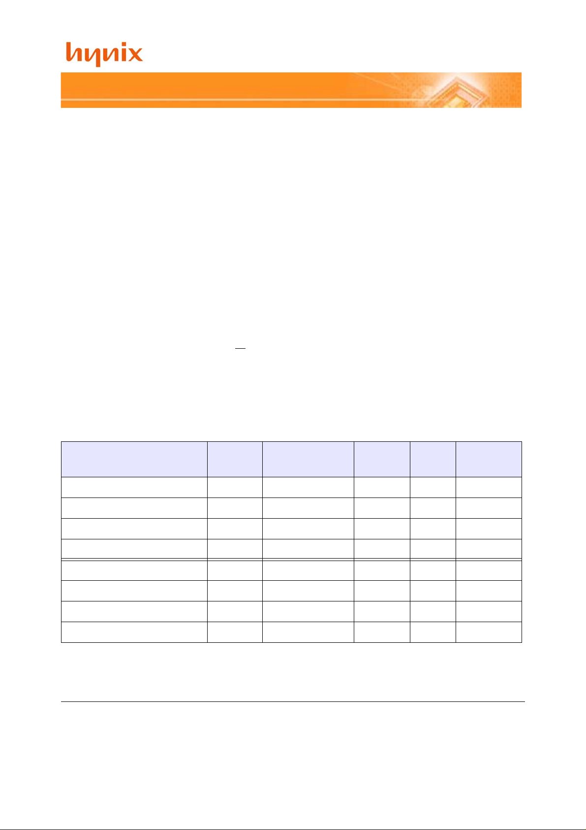
ORDERING INFORMATION
Part Name Density Organization
HYMP532S646-E3/C4 256MB 32Mx64 4 1 Leaded
HYMP564S648-E3/C4 512MB 64Mx64 8 1 Leaded
HYMP564S646-E3/C4 512MB 64Mx64 8 2 Leaded
HYMP112S64M8-E3/C4 1GB 128Mx64 16 2 Leaded
HYMP532S64P6-E3/C4 256MB 32Mx64 4 1 Lead free
HYMP564S64P8-E3/C4 512MB 64Mx64 8 1 Lead free
HYMP564S64P6-E3/C4 512MB 64Mx64 8 2 Lead free
HYMP112S64MP8-E3/C4 1GB 128Mx64 16 2 Lead free
# of
DRAMs
# of
ranks
Materials
This document is a general product description and is subject to change without notice. Hynix Semiconductor does not assume any
responsibility for use of circuits described. No patent licenses are implied.
Rev. 1.0 / Feb. 2005 1
Page 2
1200pin Unbuffered DDR2 SDRAM SO-DIMMs
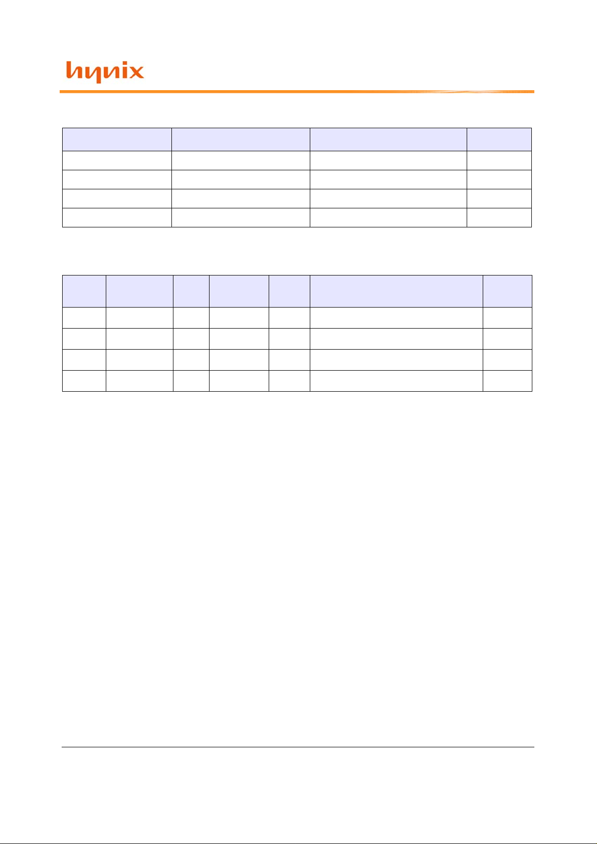
SPEED GRADE & KEY PARAMETERS
E3 (DDR2-400) C4 (DDR2-533) Unit
Speed@CL3 400 400 Mbps
Speed@CL4 400 533 Mbps
Speed@CL5 - - Mbps
CL-tRCD-tRP 3-3-3 4-4-4 tCK
ADDRESS TABLE
Density Organization Ranks SDRAMs
256MB 32M x 64 1 32Mb x 16 4 13(A0~A12)/2(BA0~BA1)/10(A0~A9) 8K / 64ms
512MB 64M x 64 2 64Mb x 8 8 14(A0~A13)/2(BA0~BA1)/10(A0~A9) 8K / 64ms
512MB 64M x 64 1 32Mb x 16 8 13(A0~A12)/2(BA0~BA1)/10(A0~A9) 8K / 64ms
1GB 128M x 64 2 64Mb x 8 16 14(A0~A13)/2(BA0~BA1)/10(A0~A9) 8K / 64ms
# of
DRAMs
# of row/bank/column Address
Refresh
Method
Rev. 1.0 / Feb. 2005 2
Page 3
1200pin Unbuffered DDR2 SDRAM SO-DIMMs
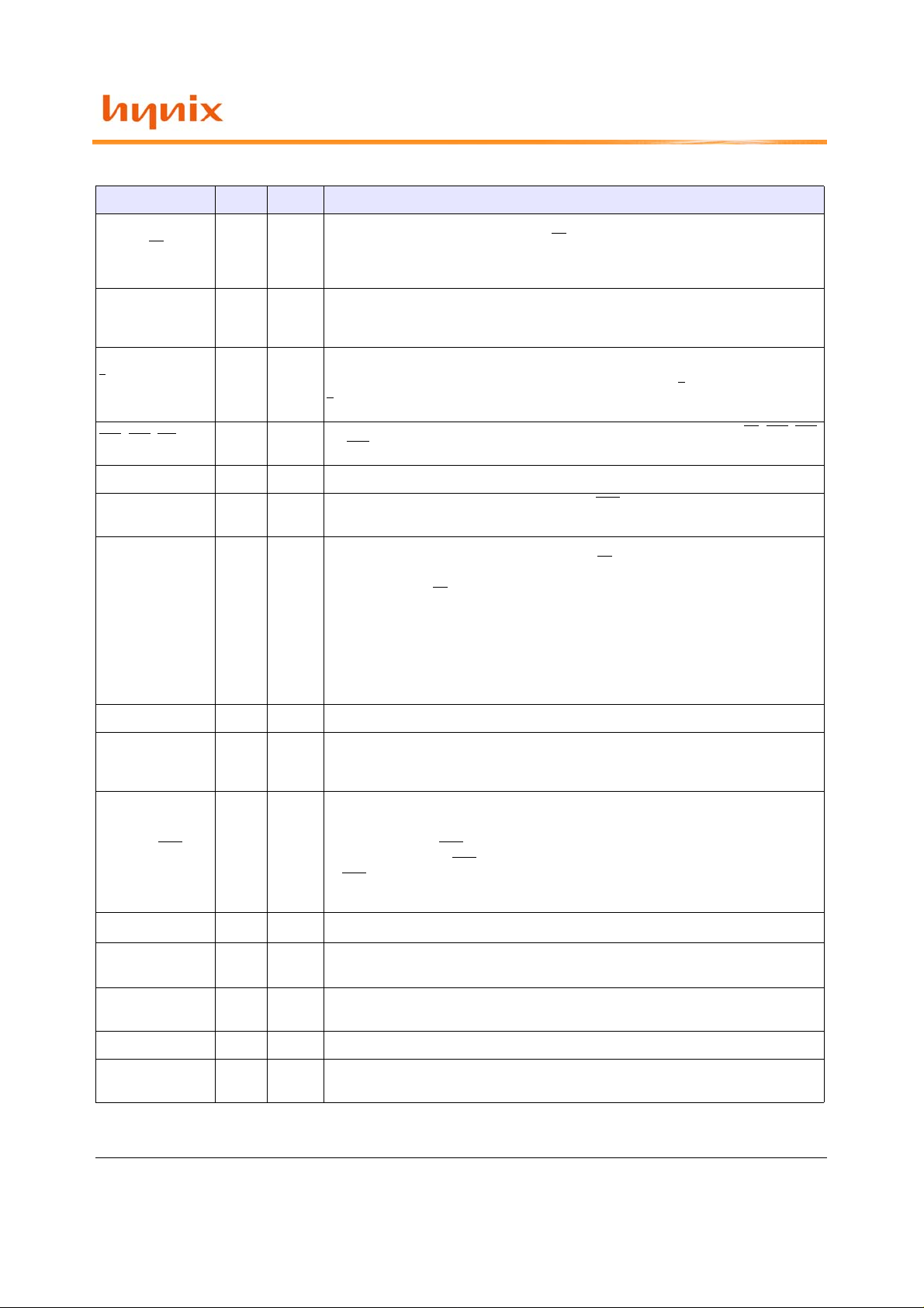
PIN DESCRIPTION
Symbol Type Polarity Pin Description
The system clock inputs. All adress an commands lines are sampled on the cross point of
CK[1:0], CK
[1:0] Input
Cross
Point
the rising edge of CK and falling edge of CK
from the clock inputs and output tim ing for read operations is synchronized to the input
clock.
. A Delay Locked Loop(DLL) circuit is driven
CKE[1:0] Input
S
[1:0] Input
RAS
, CAS, WE Input
BA[1:0] Input Selects which DDR2 SDRAM internal bank of four is activated.
ODT[1:0] Input
A[9:0], A10/AP,
A[15:11]
DQ[63:0] In/Out Data Input/Output pins.
DM[7:0] Input
Input
Active
High
Active
Low
Active
Low
Active
High
Active
High
Activates the DDR2 SDRAM CK signal when high and deactivates the CK signal when low.
By deactivating the clocks, CKE low initiates the Power Down mode or the Self Refresh
mode.
Enables the associated DDR2 SDRAM command decoder when low and disables the command decoder when high. When the command decoder is disabled, new commands are
ignored but previous operations continue. Rank 0 is selected by S
S
1
When sampled at the cross point of the ris ing edge of CK and falling ed ge of CK
and WE
define the operation to be excecuted by the SDRAM.
Asserts on-die termination for DQ, DM, DQS and DQS
SDRAM mode register.
During a Bank Activate command cycle, difines the row address when sampled at the cross
point of the rising edge of CK and falling edge of CK
cycle, defines the column address when sampled at the cr oss point of the rising edge of CK
and falling edge of CK
charge operation at the end of the burst read or write cycle. If AP is high., autoprecharge
is selected and BA0-BAn defines the bank to be precharged. If AP is low, autoprecharge is
disabled. During a Precharge command cycle., AP is used in conjunction with BA0-BAn to
control which bank(s) to precharge. If AP is high, all banks will be precharged regardless
of the state of BA0-BAn inputs. If AP is low, then BA0-BAn are used to define which bank
to precharge.
The data write masks, associated with one data byte. In Write mode , DM operates as a
byte mask by allowing input data to be written if it is low but blocks the write operation if
it is high. In Read mode, DM lines have no effect.
. In addition to the column address, AP is used to invoke autopre-
signals if enabled via the DDR2
. During a Read or Write command
0; Rank 1 is selected by
, CAS, RAS
The data strobe, associated with one data byte, sourced whit data transfers. In Write
mode, the data strobe is sourc ed by the c ontro ller and is cent ered in t he data w indo w. In
DQS[7:0], DQS
V
, VDDSPD,V
DD
SDA In/Out
SCL Input
SA[1:0] Input Address pins used to select the Serial Presence Detect base address.
TEST In/Out
Rev. 1.0 / Feb. 2005 3
[7:0] In/Out
Supply Power supplies for core, I/O, Serial Presense Detect, and ground for the module.
SS
Cross
point
Read mode, the data strobe is sourced by the DDR2 SDRAMs and is sent at leading edge
of the data window. DQS
of respective DQS and DQS
all DQS
signals must be tied on the system boar d to VS S and DDR2 SDRAM mode regis ters
programmed approriately.
This is a bidirectional pin used to transfer data int o or out of the SPD EEPROM. A resister
must be connected to V
This signals is used to clock data into and out of the SPD EEPROM. A resistor may be connected from SCL to VDD to act as a pull up.
The TEST pin is reserved for bus analysis tools and is not connected on normal memory
modules(SODIMMs).
signals are complements, and timing is relative to the crosspo int
. If the module is to be operated in single ended strobe mode,
o act as a pull up.
DD t
Page 4
1200pin Unbuffered DDR2 SDRAM SO-DIMMs
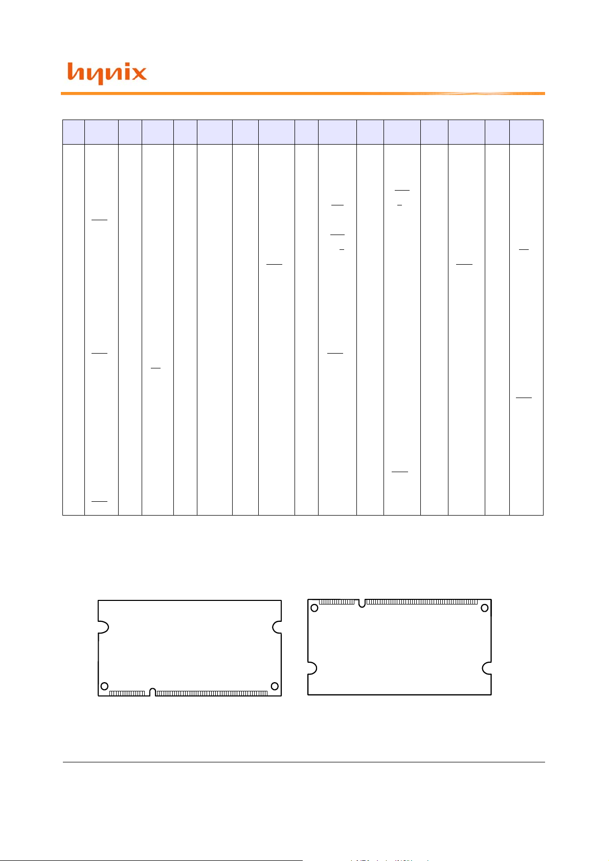
PIN ASSIGNMENT
Pin
Front
NO.
Side
1 VREF 2 VSS 51 DQS2 52 DM2 101 A1 102 A0 151 DQ42 152 DQ46
3 VSS 4 DQ4 53 VSS 54 VSS 103 VDD 104 VDD 153 DQ43 154 DQ47
5 DQ0 6 DQ5 55 DQ18 56 DQ22 105 A10/AP 106 BA1 155 VSS 156 VSS
7 DQ1 8 VSS 57 DQ19 58 DQ23 107 BA0 108 R AS
9 VSS 10 DM0 59 VSS 60 VSS 109 WE
11 DQS
13 DQS0 14 DQ6 63 DQ25 64 DQ29 113 CAS
15 VSS 16 DQ7 65 VSS 66 VSS 115 NC/S
17 DQ2 18 VSS 67 DM3 68 DQS
19 DQ3 20 DQ12 69 NC 70 DQS3 119 NC/ODT1 120 NC 169 DQS6 170 DM6
21 VSS 22 DQ13 71 VSS 72 VSS 121 VSS 122 VSS 171 VSS 172 VSS
23 DQ8 24 VSS 73 DQ26 74 DQ30 123 DQ32 124 DQ36 173 DQ50 174 DQ54
25 DQ9 26 DM1 75 DQ27 76 DQ31 125 DQ33 126 DQ37 175 DQ51 176 DQ55
27 VSS 28 VSS 77 VSS 78 VSS 127 VSS 128 VSS 177 VSS 178 VSS
29 DQS
31 DQS1 32 CK
33 VSS 34 VSS 83 NC 84 NC/A15 133 VSS 134 DQ38 183 VSS 184 VSS
35 DQ10 36 DQ14 85 BA2 86 NC/A14 135 DQ34 136 DQ39 185 DM7 186 DQS
37 DQ11 38 DQ15 87 VDD 88 VDD 137 DQ35 138 VSS 187 VSS 188 DQS7
39 VSS 40 VSS 89 A12 90 A11 139 VSS 140 DQ44 189 DQ58 190 VSS
41 VSS 42 VSS 91 A9 92 A7 141 DQ40 142 DQ45 191 DQ59 192 DQ62
43 DQ16 44 DQ20 93 A8 94 A6 143 DQ41 144 VSS 193 VSS 194 DQ63
45 DQ17 46 DQ21 95 VDD 96 VDD 145 VSS 146 DQS
47 VSS 48 VSS 97 A5 98 A4 147 DM5 148 DQS5 197 SCL 198 SA0
49 DQS
Pin
Back
Pin
Front
NO.
Side
NO.
Side
0 12 VSS 61 DQ24 62 DQ28 111 VDD 112 VDD 161 VSS 162 VSS
1 30 CK0 79 CKE0 80 NC/CKE1 129 DQS4 130 DM4 179 DQ56 180 DQ60
0 81 VDD 82 VDD 131 DQS4 132 VSS 181 DQ57 182 DQ61
2 50 NC 99 A3 100 A2 149 VSS 150 VSS 199 VDDSPD 200 SA1
Pin
NO.
Back
Side
Pin
Front
NO.
Side
3 117 VDD 118 VDD 167 DQS6 168 VSS
Pin
Back
NO.
Side
110 S0 159 DQ49 160 DQ53
114 ODT0 163 NC,TEST 164 CK1
1 116 A13 165 VSS 166 CK1
Pin
Front
NO.
5 195 SDA 196 VSS
Side
157 DQ48 158 DQ52
Pin
NO.
Back
Side
7
Pin Location
40
42
Back
2
Front
1
39
41
Rev. 1.0 / Feb. 2005 4
199
200
Page 5
1200pin Unbuffered DDR2 SDRAM SO-DIMMs
FUNCTIONAL BLOCK DIAGRAM
256MB(32Mbx64) : HYMP532S646-E3/C4
3
5%
Ω+/−
CKE0
ODT0
/S0
DQS0
/D Q S 0
DM0
DQ0
DQ1
DQ2
DQ3
DQ4
DQ5
DQ6
DQ7
DQS1
/D Q S 1
DM1
DQ8
DQ8
DQ10
DQ11
DQ12
DQ13
DQ14
DQ15
LDQS
/U D Q S
LDM
I/O 0
I/O 1
I/O 2
I/O 3
I/O 4
I/O 5
I/O 6
I/O 7
UDQS
/U D Q S
UDM
I/O 8
I/O 9
I/O 1 0
I/O 1 1
I/O 1 2
I/O 1 3
I/O 1 4
I/O 1 5
DQS2 LDQS
/D Q S 2 /LD Q S
DM2 LDM
DQ16
DQ17
DQ18
DQ19
DQ20
DQ21
DQ22
DQ23
DQS3
I/O 0
I/O 1
I/O 2
I/O 3
I/O 4
I/O 5
I/O 6
I/O 7
UDQS
/D Q S 3 /UD Q S
DM3 UD M
DQ24
DQ25
DQ26
DQ27
DQ28
DQ29
DQ30
DQ31
I/O 8
I/O 9
I/O 1 0
I/O 1 1
I/O 1 2
I/O 1 3
I/O 1 4
I/O 15
/C S O D T C K E
D0
/C S O D T C K E
D1
ODT1
CKE1
/S1
N.C.
N.C.
N.C.
DQS4
/D Q S 4
DM4
DQS5
/D Q S 5
DM5
DQS6
DQ32
DQ33
DQ34
DQ35
DQ36
DQ37
DQ38
DQ39
DQ40
DQ41
DQ42
DQ43
DQ44
DQ45
DQ46
DQ47
LDQS
/LD Q S
LDM
I/O 0
I/O 1
I/O 2
I/O 3
I/O 4
I/O 5
I/O 6
I/O 7
UDQS
/U D Q S
UDM
I/O 8
I/O 9
I/O 10
I/O 11
I/O 12
I/O 13
I/O 14
I/O 1 5
LDQS
/D Q S 6 /LD Q S
DM6 LDM
DQ48
DQ49
DQ50
DQ51
DQ52
DQ53
DQ54
DQ55
I/O 0
I/O 1
I/O 2
I/O 3
I/O 4
I/O 5
I/O 6
I/O 7
DQS7 UDQS
/D Q S 7 /U D Q S
DM7 UDM
DQ56
DQ57
DQ58
DQ59
DQ60
DQ61
DQ62
DQ63
I/O 8
I/O 9
I/O 10
I/O 11
I/O 12
I/O 13
I/O 14
I/O 1 5
/C S O D T C K E
D2
/C S O D T C K E
D3
BA0-BA1
A0-AN
/RAS
/CAS
/W E
CK0
/CK0
CK1
/CK1
3Ω +/- 5%
SDRAMS D0-3
SDRAMS D0-3
SDRAMS D0-3
SDRAMS D0-3
SDRAMS D0-3
2 loads
2 loads
SCL
SA0
SA1
VDD SPD
V
SCL
A0
Serial PD
A1
A2
REF
V
DD
V
SS
Notes :
1. Resistor values are 22 Ohm +/- 5%
SDA
WP
Serial PD
SDRAMS DO-D3
SDRAMS DO-D3, VDD and VDDQ
SDRAMS D O-D3, SPD
SDA
Rev. 1.0 / Feb. 2005 5
Page 6
1200pin Unbuffered DDR2 SDRAM SO-DIMMs
FUNCTIONAL BLOCK DIAGRAM
512MB(64Mbx64) : HYMP564S648-E3/C4
DQS0
/D Q S 0
DM0
DQS1
/D Q S 1
DM1
DQS2
/D Q S 2
DM2
DQS3
/D Q S 3
DM3
CKE0
ODT0
DQS0
DQ0
DQ1
DQ2
DQ3
DQ4
DQ5
DQ6
DQ7
DQ8
DQ8
DQ10
DQ11
DQ12
DQ13
DQ14
DQ15
DQ16
DQ17
DQ18
DQ19
DQ20
DQ21
DQ22
DQ23
DQ24
DQ25
DQ26
DQ27
DQ28
DQ29
DQ30
DQ31
3
Ω+/−
5%
DQS
/DQ S
DM
I/O 0
I/O 1
I/O 2
I/O 3
I/O 4
I/O 5
I/O 6
I/O 7
DQS
/DQ S
DM
I/O 0
I/O 1
I/O 2
I/O 3
I/O 4
I/O 5
I/O 6
I/O 7
DQS
/DQ S
DM
I/O 0
I/O 1
I/O 2
I/O 3
I/O 4
I/O 5
I/O 6
I/O 7
DQS
/DQ S
DM
I/O 0
I/O 1
I/O 2
I/O 3
I/O 4
I/O 5
I/O 6
I/O 7
/C S O D T C K E
D0
/CS O D T C K E
D1
/CS O D T C K E
D2
/CS O D T C K E
D3
/S1
ODT1
CKE1
DQS4
/DQ S4
DM4
DQS5
/D Q S 5
DM5
DQS6
/D Q S 6
DM6
DQS0
/D Q S 0
DM0
N.C.
N.C.
N.C.
DQ32
DQ33
DQ34
DQ35
DQ36
DQ37
DQ38
DQ39
DQ40
DQ41
DQ42
DQ43
DQ44
DQ45
DQ46
DQ47
DQ48
DQ49
DQ50
DQ51
DQ52
DQ53
DQ54
DQ55
DQ56
DQ57
DQ58
DQ59
DQ60
DQ61
DQ62
DQ63
DQS
/DQ S
DM
I/O 0
I/O 1
I/O 2
I/O 3
I/O 4
I/O 5
I/O 6
I/O 7
DQS
/DQ S
DM
I/O 0
I/O 1
I/O 2
I/O 3
I/O 4
I/O 5
I/O 6
I/O 7
DQS
/DQ S
DM
I/O 0
I/O 1
I/O 2
I/O 3
I/O 4
I/O 5
I/O 6
I/O 7
DQS
/DQ S
DM
I/O 0
I/O 1
I/O 2
I/O 3
I/O 4
I/O 5
I/O 6
I/O 7
/CS O D T C K E
D4
/C S O D T C K E
D5
/C S O D T C K E
D6
/C S O D T C K E
D7
BA0-BA1
A0-AN
/R A S
/C A S
/W E
CK0
/CK 0
CK1
/CK 1
3Ω +/- 5%
SDRAMS D 0-7
SDRAMS D 0-7
SDRAMS D 0-7
SDRAMS D 0-7
SDRAMS D 0-7
4 loads
4 loads
SCL
SA0
SA1
VDD SPD
SCL
A0
Serial PD
A1
A2
V
REF
V
DD
V
SS
Notes :
1. Resistor values are 22 Ohm +/- 5%
WP
SDA
SDA
Serial PD
SDRAMS DO-D7
SDRAMS DO-D7, VDD and VDDQ
SDRAMS DO -D7, SPD
Rev. 1.0 / Feb. 2005 6
Page 7
1200pin Unbuffered DDR2 SDRAM SO-DIMMs
FUNCTIONAL BLOCK DIAGRAM
512MB(64Mbx64): HYMP564S646-E3/C4
DQS0
/DQS0
DM0
DQS1
/DQS1
DM1
DQS2
/DQS2
DM2
DQS3
/DQS3
DM3
ODT1
ODT0
CKE1
CKE0
/S1
/S0
DQ0
DQ1
DQ2
DQ3
DQ4
DQ5
DQ6
DQ7
DQ8
DQ8
DQ10
DQ11
DQ12
DQ13
DQ14
DQ15
DQ16
DQ17
DQ18
DQ19
DQ20
DQ21
DQ22
DQ23
DQ24
DQ25
DQ26
DQ27
DQ28
DQ29
DQ30
DQ31
3 Ω+/− 5%
LDQS
/ UDQS
LDM
I/ O 0
I/ O 1
I/ O 2
I/ O 3
I/ O 4
I/ O 5
I/ O 6
I/O 7
UDQS
/ UDQS
UDM
I/ O 8
I/ O 9
I/ O 10
I/ O 11
I/ O 12
I/ O 13
I/ O 14
I/ O 15
LDQS
/LDQS
LDM
I/ O 0
I/ O 1
I/ O 2
I/ O 3
I/ O 4
I/ O 5
I/ O 6
I/ O 7
UDQS
/UDQS
UDM
I/ O 8
I/ O 9
I/ O 10
I/ O 11
I/ O 12
I/ O 13
I/ O 14
I/ O 15
/CS
/CS
D0
D1
CKE
CKE
CKE
ODT
LDQS
/UDQS
LDM
I/ O 0
I/ O 1
I/ O 2
I/ O 3
I/ O 4
I/ O 5
I/ O 6
I/ O 7
UDQS
/UDQS
UDM
I/ O 8
I/ O 9
I/ O 10
I/ O 11
I/ O 12
I/ O 13
I/ O 14
I/ O 15
ODT
LDQS
/UDQS
LDM
I/ O 0
I/ O 1
I/ O 2
I/ O 3
I/ O 4
I/ O 5
I/ O 6
I/ O 7
UDQS
/UDQS
UDM
I/ O 8
I/ O 9
I/ O 10
I/ O 11
I/ O 12
I/ O 13
I/ O 14
I/ O 15
/CS
/CS
D4
D5
ODT
CKE
ODT
DQS4
/DQS4
DM4
DQS5
/DQS5
DM5
DQS6
/DQS6
DM6
DQS7
/DQS7
DM7
DQ32
DQ33
DQ34
DQ35
DQ36
DQ37
DQ38
DQ39
DQ40
DQ41
DQ42
DQ43
DQ44
DQ45
DQ46
DQ47
DQ48
DQ49
DQ50
DQ51
DQ52
DQ53
DQ54
DQ55
DQ56
DQ57
DQ58
DQ59
DQ60
DQ61
DQ62
DQ63
LDQS
/UDQS
LDM
I/ O 0
I/ O 1
I/ O 2
I/ O 3
I/ O 4
I/ O 5
I/ O 6
I/ O 7
UDQS
/UDQS
UDM
I/ O 8
I/ O 9
I/ O 10
I/ O 11
I/ O 12
I/ O 13
I/ O 14
I/ O 15
LDQS
/LDQS
LDM
I/ O 0
I/ O 1
I/ O 2
I/ O 3
I/ O 4
I/ O 5
I/ O 6
I/ O 7
UDQS
/UDQS
UDM
I/ O 8
I/ O 9
I/ O 10
I/ O 11
I/ O 12
I/ O 13
I/ O 14
I/ O 15
/CS
/CS
D2
D3
CKE
CKE
ODT
LDQS
/ UDQS
LDM
I/ O 0
I/ O 1
I/ O 2
I/ O 3
I/ O 4
I/ O 5
I/ O 6
I/ O 7
UDQS
/ UDQS
UDM
I/ O 8
I/ O 9
I/ O 10
I/ O 11
I/ O 12
I/ O 13
I/ O 14
I/ O 15
ODT
LDQS
/ UDQS
LDM
I/ O 0
I/ O 1
I/ O 2
I/ O 3
I/ O 4
I/ O 5
I/ O 6
I/ O 7
UDQS
/ UDQS
UDM
I/ O 8
I/ O 9
I/ O 10
I/ O 11
I/ O 12
I/ O 13
I/ O 14
I/ O 15
/CS
/CS
D6
D7
CKE
ODT
CKE
ODT
BA0 - BA1
A0-AN
/RAS
/CAS
/WE
CK0
/CK0
CK1
/CK1
3Ω +/- 5%
SDRAMS D0-7
SDRAMS D0-7
SDRAMS D0-7
SDRAMS D0-7
SDRAMS D0-7
4 loads
4 loads
SCL
SA0
SA1
VDD SPD
V
REF
V
V
SCL
A0
Serial PD
A1
A2
DD
SS
WP
SDA
SDA
Serial PD
SDRAMS DO-D3
SDRAMS DO-D3, VDD and VDDQ
SDRAMS DO
-D3, SPD
Notes :
1. Resistor values are 22 Ohm +/- 5%
Rev. 1.0 / Feb. 2005 7
Page 8

1200pin Unbuffered DDR2 SDRAM SO-DIMMs
FUNCTIONAL BLOCK DIAGRAM
1GB(128Mbx64) : HYMP112S64M8-E3/C4
3 Ω+/− 5%
CKE1
ODT1
/S1
CKE0
ODT0
/S0
DQS0
/DQS0
DM0
DQS1
/DQS1
DM1
DQS2
/DQS2
DM2
DQS3
/DQS3
DM3
DQ0
DQ1
DQ2
DQ3
DQ4
DQ5
DQ6
DQ7
DQ8
DQ8
DQ 10
DQ 11
DQ 12
DQ 13
DQ 14
DQ 15
DQ 16
DQ 17
DQ 18
DQ 19
DQ 20
DQ 21
DQ 22
DQ 23
DQ 24
DQ 25
DQ 26
DQ 27
DQ 28
DQ 29
DQ 30
DQ 31
DQS
/DQS
DM
I/O 0
I/O 1
I/O 2
I/O 3
I/O 4
I/O 5
I/O 6
I/O 7
DQS
/DQS
DM
I/ O 0
I/ O 1
I/ O 2
I/ O 3
I/ O 4
I/ O 5
I/ O 6
I/O 7
DQS
/DQS
DM
I/ O 0
I/ O 1
I/ O 2
I/ O 3
I/ O 4
I/ O 5
I/ O 6
I/O 7
DQS
/DQS
DM
I/ O 0
I/ O 1
I/ O 2
I/ O 3
I/ O 4
I/ O 5
I/ O 6
I/O 7
D0,D8(DDP)
/CS 0 ODT 0 CKE0 /CS 1 ODT 1 CKE1
D1,D9(DDP)
/CS 0 ODT 0 CKE0 /CS 1 ODT 1 CKE1
D2,D10( DDP)
/CS 0 ODT 0 CKE0 /CS 1 ODT 1 CKE1
D3,D11( DDP) D7,D15(DDP)
DQS 4
/DQS4
DM4
DQS 5
/DQS5
DM5
DQS 6
/DQS6
DM6
DQS 7
/DQS7
DM7
DQ 32
DQ 33
DQ 34
DQ 35
DQ 36
DQ 37
DQ 38
DQ 39
DQ 40
DQ 41
DQ 42
DQ 43
DQ 44
DQ 45
DQ 46
DQ 47
DQ 48
DQ 49
DQ 50
DQ 51
DQ 52
DQ 53
DQ 54
DQ 55
DQ 56
DQ 57
DQ 58
DQ 59
DQ 60
DQ 61
DQ 62
DQ 63
DQS
/CS 0 ODT 0 CKE0 /CS 1 ODT 1 CKE1/CS 0 ODT 0 CKE 0 /CS 1 ODT 1 CKE1
/DQS
DM
I/ O 0
I/ O 1
I/ O 2
I/ O 3
I/ O 4
I/ O 5
I/ O 6
I/ O 7
DQS
/DQS
DM
I/ O 0
I/ O 1
I/ O 2
I/ O 3
I/ O 4
I/ O 5
I/ O 6
I/ O 7
DQS
/DQS
DM
I/ O 0
I/ O 1
I/ O 2
I/ O 3
I/ O 4
I/ O 5
I/ O 6
I/ O 7
DQS
/DQS
DM
I/ O 0
I/ O 1
I/ O 2
I/ O 3
I/ O 4
I/ O 5
I/ O 6
I/ O 7
D4,D12(DDP)
/CS 0 ODT 0 CKE0 /CS 1 ODT 1 CKE1
D5,D13(DDP)
/CS 0 ODT 0 CKE0 /CS 1 ODT 1 CKE1
D6,D14(DDP)
/CS 0 ODT 0 CKE0 /CS 1 ODT 1 CKE1
BA0 - BA1
A0-AN
CK0
/CK 0
CK1
/CK1
/RAS
/ CAS
/WE
9.1 pF
9.1 pF
10Ω+/-5 %
8 loads
8 loads
8 loads
8 loads
SDRAMS D 0-15
SDRAMS D 0-15
SDRAMS D 0-15
SDRAMS D 0-15
SDRAMS D 0-15
VDD SPD
SCL
SA0
SA1
:
V
REF
V
DD
V
SS
SCL
A0
Serial PD
A1
A2
Serial PD
SDRAMS DO-D15
SDRAMS DO-D15 , VDD and VDDQ
SDRAMS DO-D15 , SPD
WP
SDA
SDA
Notes :
1. Resistor values are 22 Ohm +/- 5%
Rev. 1.0 / Feb. 2005 8
Page 9

ABSOLUTE MAXIMUM RATINGS
Parameter Symbol Value Unit Note
1200pin Unbuffered DDR2 SDRAM SO-DIMMs
Voltage on V
Voltage on V
pin relative to Vss
DD
pin relative to Vss
DDQ
Voltage on any pin relative to Vss
Storage Temperature
Storage Humidity(without condensation)
V
DD
V
- 0.5 V ~ 2.3 V V 1
DDQ
V
IN, VOUT
T
STG
H
STG
- 1.0 V ~ 2.3 V V 1
- 0.5 V ~ 2.3 V V 1
-50 ~ +100
o
C
5 to 95 % 1
1
Notes:
1. Stress greater than those listed may cause permanent damage to the device. This is a stress r ating only, and device
functional operation at or above the conditions indicated is not implied. Expousure to absolute maximum rating con
ditions for extended periods may affect reliablility.
OPERATING CONDITIONS
Parameter Symbol Rating Units Notes
DIMM Operating temperature(ambient)
DIMM Barometric Pressure(operating & storage)
DRAM Component Case Temperature Range
Notes:
1. Up to 9850 ft.
o
2. If the DRAM case temperature is Above 85
C, the Auto-Refresh command interval has to be reduced to
tREFI=3.9us. For Measurement conditions of T
T
OPR
BAR
P
T
CASE
, please refer to the JEDEC document JESD51-2.
CASE
0 ~ +55
105 to 69 K Pascal 1
0 ~+95
o
C
o
C 2
DC OPERATING CONDITIONS (SSTL_1.8)
Parameter Symbol Min Max Unit Note
V
Power Supply Voltage
Input Reference Voltage V
EEPROM Supply Voltage V
Termination Voltage
DD
V
DDQ
REF
DDSPD
V
TT
Notes:
must be less than or equal to VDD.
1. V
DDQ
2. Peak to peak ac noise on V
may not exeed +/-2% V
REF
3. VTT of transmitting device must track VREF of receiving device.
Rev. 1.0 / Feb. 2005 9
1.7 1.9 V
1.7 1.9 V 1
0.49 x V
DDQ
0.51 x V
DDQ
V2
1.7 3.6 V
V
V
-0.04
REF
(dc)
REF
+0.04 V 3
REF
Page 10

INPUT DC LOGIC LEVEL
Parameter Symbol Min Max Unit Note
1200pin Unbuffered DDR2 SDRAM SO-DIMMs
Input High Voltage V
Input Low Voltage V
(DC) V
IH
(DC) -0.30 V
IL
+ 0.125 V
REF
+ 0.3 V
DDQ
- 0.125 V
REF
INPUT AC LOGIC LEVEL
Parameter Symbol Min Max Unit Note
AC Input logic High V
AC Input logic Low V
IH
IL
(AC)
(AC)
+ 0.250 -
V
REF
-V
REF
- 0.250
V
V
AC INPUT TEST CONDITIONS
Symbol Condition Value Units Notes
V
REF
V
SWING(MAX)
SLEW Input signal minimum slew rate 1.0 V/ns 2, 3
Notes:
1. Input waveform timing is referenced to the input signal crossing through the V
under test.
2. The input signal minimum slew rate is to be maintained over the range from V
and the range from V
3. AC timings are referenced with input waveforms switching from VIL(ac) to VIH(ac) on the positive transitions
and VIH(ac) to VIL(ac) on the negative transitions.
Input reference voltage 0.5 * V
Input signal maximum peak to peak swing 1.0 V 1
REF
to V
IL(ac) max
for falling edges as shown in the below figure.
DDQ
REF
REF
V1
level applied to the device
to V
IH(ac) min
for rising edges
V
DDQ
V
SWING(MAX)
V
V
V
V
V
V
IH(ac)
IH(dc)
REF
IL(dc)
IL(ac)
SS
min
min
max
max
delta TRdelta TF
V
min
V
-
V
Falling Slew = Rising Slew =
REF
delta TF
max
IL
(ac)
IH
delta TR
(ac)
- V
REF
< Figure : AC Input Test Signal Waveform>
Rev. 1.0 / Feb. 2005 10
Page 11

1200pin Unbuffered DDR2 SDRAM SO-DIMMs
Differential Input AC logic Level
Symbol Parameter Min. Max. Units Note
(ac)
V
ID
V
(ac)
IX
ac differential input voltage
ac differential cross point voltage
0.5 * V
1. VIN(DC) specifies the allowable DC execution of each input of differential pair such as CK, CK, DQS, DQS, LDQS,
LDQS
2. V
(such as CK, DQS, LDQS or UDQS) level and V
The minimum value is equal to V
, UDQS and UDQS.
(DC) specifies the input differential voltage |VTR -VCP | required for switching, where VTR is the true input
ID
is the complementary input (such as CK, DQS, LDQS or UDQS) level.
CP
(DC) - VIL(DC).
IH
V
V
TR
V
CP
0.5 V
- 0.175 0.5 * V
DDQ
DDQ
V
ID
DDQ
Crossing point
V
IX or VOX
+ 0.6 V 1
+ 0.175 V 2
DDQ
V
SSQ
< Differential signal levels >
Notes:
1. V
(AC) specifies the input differential voltage |VTR -VCP | required for switching, where VTR is the true input signal
ID
(such as CK, DQS, LDQS or UDQS) and V
The minimum value is equal to V
2. The typical value of V
track variations in V
(AC) is expected to be about 0.5 * V
IX
. VIX(AC) indicates the voltage at whitch differential input signals must cross.
DDQ
(AC) - VIL(AC).
IH
is the complementary input signal (such as CK, DQS, LDQS or UDQS).
CP
of the transmitting device and VIX(AC) is expected to
DDQ
DIFFERENTIAL AC OUTPUT PARAMETERS
Symbol Parameter Min. Max. Units Note
(ac)
V
OX
ac differential cross point voltage
Notes:
1. The typical value of V
track variations in V
(AC) is expected to be about 0.5 * V
OX
. VOX(AC) indicates the voltage at whitch differential output signals must cross.
DDQ
0.5 * V
- 0.125 0.5 * V
DDQ
of the transmitting device and VOX(AC) is expected to
DDQ
+ 0.125 V 1
DDQ
Rev. 1.0 / Feb. 2005 11
Page 12

1200pin Unbuffered DDR2 SDRAM SO-DIMMs
OUTPUT BUFFER LEVELS
OUTPUT AC TEST CONDITIONS
Symbol Parameter SSTL_18 Units Notes
V
OTR
Output Timing Measurement Reference Level 0.5 * V
DDQ
V1
Notes:
1. The VDDQ of the device under test is referenced.
OUTPUT DC CURRENT DRIVE
Symbol Parameter SSTl_18 Units Notes
I
OH(dc)
I
OL(dc)
Notes:
1. V
V
2. V
= 1.7 V; V
DDQ
- 280 mV.
DDQ
= 1.7 V; V
DDQ
3. The dc value of V
4. The values of IOH(dc) and IOL(dc) are based on the conditions given in Notes 1 and 2. They are used to test device
drive current capability to ensure V
SSTL_18 receiver.
The actual current values are derived by shifting the desired driver operating point along a 21 ohm load line to define
a convenient driver current for measurement.
Output Minimum Source DC Current - 13.4 mA 1, 3, 4
Output Minimum Sink DC Current 13.4 mA 2, 3, 4
= 1420 mV. (V
OUT
= 280 mV. V
OUT
applied to the receiving device is set to V
REF
- V
OUT
OUT/IOL
min plus a noise margin and VIL max minus a noise margin are delivered to an
IH
)/IOH must be less than 21 ohm for values of V
DDQ
must be less than 21 ohm for values of V
TT
between 0 V and 280 mV.
OUT
between V
OUT
DDQ
and
Rev. 1.0 / Feb. 2005 12
Page 13

1200pin Unbuffered DDR2 SDRAM SO-DIMMs
PIN Capacitance (VDD=1.8V,VDDQ=1.8V, TA=25℃. f=1MHz )
256MB : HYMP532S64[P]6
Pin Symbol Min Max Unit
CK, CK
CKE, ODT,CS CI1 27 30 pF
Address, RAS
DQ, DM, DQS, DQS
, CAS, WE CI2 25 32 pF
CCK 12 15 pF
CIO 6.0 7.5 pF
512MB : HYMP564S64[P]8
Pin Symbol Min Max Unit
CK, CK
CKE, ODT, CS CI1 24 38 pF
Address, RAS
DQ, DM, DQS, DQS
, CAS, WE CI2 23 40 pF
CCK 13 21 pF
CIO 5 8 pF
512MB : HYMP564S64[P]6
Pin Symbol Min Max Unit
CK, CK
CKE, ODT,CS CI1 22 25 pF
Address, RAS
DQ, DM, DQS, DQS
, CAS, WE CI2 28.5 37.0 pF
CCK 17 20 pF
CIO 10.0 12.0 pF
1GB : HYMP512S64M[P]8
Pin Symbol Min Max Unit
CK, CK
CKE, ODT,CS CI1 32 58 pF
Address, RAS
DQ, DM, DQS, DQS
Notes:
1. Pins not under test are tied to GND.
2. These value are guaranteed by design and tested on a sample basis only.
Rev. 1.0 / Feb. 2005 13
, CAS, WE CI2 47 96 pF
CCK 25 49 pF
CIO 16 20 pF
Page 14

1200pin Unbuffered DDR2 SDRAM SO-DIMMs
IDD SPECIFICATIONS (T
: 0 to 95oC)
CASE
256MB, 32M x 64 SO- DIMM : HYMP532S64[P]6
Symbol E3(DDR2 400@CL 3) C4(DDR2 533@CL 4) Unit note
IDD0 500 520 mA
IDD1 540 560 mA
IDD2P 24 28 mA
IDD2Q 140 160 mA
IDD2N 160 180 mA
IDD3P(F) 80 100 mA
IDD3P(S) 20 24 mA
IDD3N 260 300 mA
IDD4R 600 760 mA
IDD4W 720 880 mA
IDD5B 660 700 mA
IDD6 22 22 mA 1
IDD6(L) 12 12 mA 1
IDD7 1320 1320 mA
512MB, 64M x 64 SO- DIMM : HYMP564S64[P]8
Symbol E3(DDR2 400@CL3) C4(DDR2 533@CL 4) Unit note
IDD0 640 720 mA
IDD1 720 800 mA
IDD2P 48 56 mA
IDD2Q 280 320 mA
IDD2N 320 360 mA
IDD3P(F) 160 200 mA
IDD3P(S) 40 48 mA
IDD3N 440 520 mA
IDD4R 1040 1280 mA
IDD4W 1200 1440 mA
IDD5B 1320 1400 mA
IDD6 44 44 mA 1
IDD6(L) 32 32 mA 1
IDD7 1760 1760 mA
Notes:
1. IDD6 current values are guaranted up to Tcase of 85℃ max.
Rev. 1.0 / Feb. 2005 14
Page 15

1200pin Unbuffered DDR2 SDRAM SO-DIMMs
512MB, 64M x 64 SO - DIMM : HYMP564S64[P]6
Symbol E3(DDR2 400@CL 3) C4(DDR2 533@CL 4) Unit note
IDD0 760 820 mA
IDD1 800 860 mA
IDD2P 48 56 mA
IDD2Q 280 320 mA
IDD2N 320 360 mA
IDD3P(F) 160 200 mA
IDD3P(S) 40 48 mA
IDD3N 520 600 mA
IDD4R 860 1060 mA
IDD4W 980 1180 mA
IDD5B 920 1000 mA
IDD6 44 44 mA 1
IDD6(L) 32 32 mA 1
IDD7 1580 1620 mA
1GB, 128M x 64 SO - DIMM : HYMP112S64M[P]8
Symbol E3(DDR2 400@CL 3) C4(DDR2 533@CL 4) Unit note
IDD0 1080 1240 mA
IDD1 1160 1320 mA
IDD2P 96 112 mA
IDD2Q 560 640 mA
IDD2N 640 720 mA
IDD3P(F) 320 400 mA
IDD3P(S) 80 96 mA
IDD3N 880 1040 mA
IDD4R 1480 1800 mA
IDD4W 1640 1960 mA
IDD5B 1760 1920 mA
IDD6 88 88 mA 1
IDD6(L) 64 64 mA 1
IDD7 2200 2280 mA
Notes:
1. IDD6 current values are guaranted up to Tcase of 85℃ max.
Rev. 1.0 / Feb. 2005 15
Page 16

1200pin Unbuffered DDR2 SDRAM SO-DIMMs
IDD Meauarement Conditions
Symbol Conditions
IDD0
IDD1
IDD2P
IDD2Q
IDD2N
IDD3P
IDD3N
IDD4W
IDD4R
IDD5B
IDD6
IDD7
Operating one bank active-precharge current; tCK = tCK(IDD), tRC = tRC(IDD), tRAS = tRAS-
min(IDD);CKE is HIGH, CS
inputs are SWITCHING
Operating one bank active-read-precharge curren ; IOUT = 0mA;BL = 4, CL = CL(IDD), AL = 0;
t
CK = tCK(IDD), tRC = tRC (IDD), tRAS = tRASmin(IDD), tRCD = tRCD(IDD) ; CKE is HIGH, CS
between valid commands ; Address bus inputs are SWITCHING ; Data pattern is same as IDD4W
Precharge power-down current ; All banks idle ; tCK = tCK(IDD) ; CKE is LOW ; Other control and address
bus inputs are STABLE; Data bus inputs are FLOATING
Precharge quiet standby current;All banks idle; tCK = tCK(IDD);CKE is HIGH, CS
address bus inputs are STABLE; Data bus inputs are FLOATING
Precharge standby current; All banks idle; tCK = tCK(IDD); CKE is HIGH, CS
address bus inputs are SWITCHING; Data bus inputs are SWITCHING
Active power-down current; All banks open; tCK = tCK(IDD); CKE is LOW;
Other control and address bus inputs are STABLE; Data bus inputs are FLOATING
Active standby current; All banks open; tCK = tCK(IDD), tRAS = tRASmax(IDD), tRP =tRP(IDD); CKE is
HIGH, CS
inputs are SWITCHING
Operating burst write current; All banks open, Continuous burst writes; BL = 4, CL = CL(IDD), AL = 0; tCK
= tCK(IDD), tRAS = tRASmax(IDD), tRP = tRP(IDD); CKE is HIGH, CS
Address bus inputs are SWITCHING; Data bus inputs are SWITCHING
Operating burst read current; All banks open, Continuous burst r eads, IOU T = 0mA; BL = 4, CL = CL(IDD ),
AL = 0; tCK = tCK(IDD), tRAS = tRASmax(IDD), tRP = tRP(IDD); CKE is HIGH, CS
mands; Address bus inputs are SWITCHING;; Data pattern is same as IDD4W
Burst refresh current; tCK = tCK(IDD); Refresh command at every tRFC(IDD) interval; CKE is HIGH, CS
HIGH between valid commands; Other control and address bus inputs are SWITCHING; Data bus inputs are
SWITCHING
Self refresh current; CK and CK
bus inputs are FLOATING. IDD6 current values are guaranted up to Tcase of 85℃ max.
Operating bank interleave read current; All bank interleaving reads, IOUT = 0mA; BL = 4, CL = CL(IDD),
AL = tRCD(IDD)-1*tCK(IDD); tCK = tCK(IDD), tRC = tRC(IDD), tRRD = tRRD(IDD), tRCD = 1*tCK(IDD); CKE is
HIGH, CS
same as IDD4R; - Refer to the following page for detailed timing conditions
is HIGH between valid commands; Other control and address bus inputs are SWITCHING; Data bus
is HIGH between valid commands; Addres s bus inputs are STABLE during DESELECTs; Data pattern is
is HIGH between valid commands;Address bus inputs are SWITCHING;Data bus
at 0V; CKE ≤ 0.2V; Other control and address bus input s are FLOATING; Data
is HIGH
is HIGH; Other control and
is HIGH; Other control and
Fast PDN Exit MRS(12) = 0
Slow PDN Exit MRS(12) = 1
is HIGH between valid commands;
is HIGH between valid com-
Units
mA
mA
mA
mA
mA
mA
mA
mA
mA
mA
is
mA
mA
mA
Notes:
1. IDD specifications are tested after the device is properly initialized
2. Input slew rate is specified by AC Parametric Test Condition
3. IDD parameters are specified with ODT disabled.
4. Data bus consists of DQ, DM, DQS, DQS
of EMRS bits 10 and 11.
5. Definitions for IDD
LOW is defined as Vin ≤ VILAC(max)
HIGH is defined as Vin ≥ VIHAC(min)
STABLE is defined as inputs stable at a HIGH or LOW level
FLOATING is defined as inputs at VREF = VDDQ/2
SWITCHING is defined as: inputs changing between HIGH and LOW every other clock cycle (once per two clocks) for address and
control signals, and inputs changing between HIGH and LOW every other data transfer (once per clock)
for DQ signals not including masks or strobes.
Rev. 1.0 / Feb. 2005 16
, RDQS, RDQS, LDQS, LDQS, UDQS, and UDQS. IDD values must be met with all combinations
Page 17

1200pin Unbuffered DDR2 SDRAM SO-DIMMs
Electrical Characteristics & AC Timings
Speed Bins and CL,tRCD,tRP,tRC and tRAS for Corresponding Bin
Speed DDR2-533 (C4) DDR2-400 (E3) Unit
Bin(CL-tRCD-tRP) 4-4-4 3-3-3
Parameter min min
CAS Latency 4 3 ns
tRCD 15 15 ns
tRP 15 15 ns
tRC 60 55 ns
tRAS 45 40 ns
AC Timing Parameters by Speed Grade
Parameter Symbol
Data-Out edge to Clock edge Skew tAC -600 600 -500 500 ps
DQS-Out edge to Clock edge Skew tDQSCK -500 500 -450 450 ns
Clock High Level Width tCH 0.45 0.55 0.45 0.55 CK
Clock Low Level Width tCL 0.45 0.55 0.45 0.55 CK
Clock Half Period tHP
System Clock Cycle Time tCK 5000 800 0 3750 8000 ps
DQ and DM input setup time tDS 275 - 225 - ps 1
DQ and DM input hold time tDH 150 - 100 - ps 1
DQ and DM input setup time(single-ended strobe) tDS1
DQ and DM input hold time(single-ended strobe) tDH1
Control & Address input Pulse Width for each input tIPW 0.6 - 0.6 - tCK
DQ and DM input pulse witdth for each input pulse
width for each input
Data-out high-impedance window from CK, /CK tHZ
DQS low-impedance time from CK/CK tLZ(DQS) tAC min tAC max tAC min tAC max ps
DQ low-impedance time from CK/CK tLZ(DQ) 2*tAC min tAC max 2*tAC min tAC max ps
DQS-DQ skew for DQS and associated DQ signals tDQSQ - 350 - 300 ps
DQ hold skew factor tQHS - 450 - 400 ps
DQ/DQS output hold time from DQS tQH tHP - tQHS - tHP - tQHS - ps
First DQS latching transition to associated clock edge tDQSS -0.25 +0.25 -0.25 +0.25 tCK
DQS input high pulse width tDQSH 0.35 - 0.35 - tCK
DQS input low pulse width tDQSL 0.35 - 0.35 - tCK
DQS falling edge to CK setup time tDSS 0.2 - 0.2 - tCK
DQS falling edge hold time from CK tDSH 0.2 - 0.2 - tCK
Mode register set command cycle time tMRD 2 - 2 - tCK
Write postamble tWPST 0.4 0.6 0.4 0.6 tCK
Write pr eamble tWPRE 0.35 - 0.35 - tCK
tDIPW 0.35 - 0.35 - tCK
DDR2-400 DDR2-533
Min Max Min Max
min
(tCL,tCH)
-tAC max-tAC max
-
min
(tCL,tCH)
-ns
Unit Note
ps
Rev. 1.0 / Feb. 2005 17
Page 18

1200pin Unbuffered DDR2 SDRAM SO-DIMMs
- Continued -
Parameter Symbol
DDR2-400 DDR2-533
Min Max Min Max
Unit Note
Address and control input setup time tIS 350 -250- ps
Address and control input hold time tIH 475 -375- ps
Read preamble tRPRE 0.9 1.1 0.9 1.1 tCK
Read postamble tRPST 0.4 0.6 0.4 0.6 tCK
Auto-Refresh to Active/Auto-Refresh command
period
tRFC 105 - 105 - ns
Row Active to Row Active Delay for 1KB page size tRRD 7.5 - 7.5 - ns
Row Active to Row Active Delay for 2KB page size tRRD 10 - 10 - ns
Four Activate Window for 1KB page size tFAW 37.5 - 37.5 - ns
Four Activate Window for 2KB page size tFAW 50 - 50 - ns
CAS to CAS command delay tCCD 2 2 tCK
Write recovery time tWR 15 -15- ns
Auto Precharge Write Recovery + Precharge Time tDAL tWR+tRP - tWR+tRP - tCK
Write to Read Command Delay tWTR 10 -
7.5
-
ns
Internal read to precharge command delay tRTP 7.5 7.5 ns
Exit self refresh to a non-read command tXSNR tRFC + 10 tRFC + 10 ns
Exit self refresh to a read command tXSRD 200 - 200 - tCK
Exit precharge power down to any non-read
command
tXP 2 - 2 - tCK
Exit active power down to read command tXARD 2 2 tCK
Exit active power down to read command
(Slow exit, Lower power)
CKE minimum pulse width
(high and low pulse width)
ODT turn-on delay
ODT turn-on
ODT turn-on(Power-Down mode)
ODT turn-off delay
ODT turn-off
ODT turn-off (Power-Down mode)
tXARDS 6 - AL 6 - AL tCK
t
CKE
t
AOND
t
AON
t
AONPD
t
AOFD
t
AOF
t
AOFPD
3
2222tCK
tAC(min)
tAC(min)+2
tAC(max)+
1
2tCK+tAC(
max)+1
2.5 2.5 2.5 2.5 tCK
tAC(min)
tAC(min)+2
tAC(max)+
0.6
2.5tCK+tA
C(max)+1
3 tCK
tAC(min)
tAC(min)+2
tAC(min)
tAC(min)+2
tAC(max)+
2tCK+tAC(
max)+1
tAC(max)+
0.6
2.5tCK+tA
C(max)+1
1
ns
ns
ns
ns
ODT to power down entry latency tANPD 3 3 tCK
ODT power down exit latency tAXPD 8 8 tCK
OCD drive mode output delay tOIT 0 12 0 12 ns
Minimum time clocks remains ON after CKE
asynchronously drops LOW
Average periodic Refresh Interval
tDelay tIS+tCK+tIH tIS+tCK+tIH ns
tREFI - 7.8 - 7.8 us 2
tREFI - 3.9 - 3.9 us 3
Notes:
1. For details and notes, please refer to the relevant Hyni x component datasheet(HY5PS12[8/16]21(L)F).
2. 0°C ≤ TCASE ≤ 85°C
3. 85°C < TCASE ≤ 95°C
Rev. 1.0 / Feb. 2005 18
Page 19

PACKAGE OUTLINE
32Mx64 - HYMP532S64[P]6
20.00 Min
4.00 +/-0.10
1200pin Unbuffered DDR2 SDRAM SO-DIMMs
Front
67.60
Side
3.80 max
30.00
20.00
2.45
PIN
PIN
1
11.40
2.70
4.20
11.40
2.40
2
PIN
PIN
40
39
4.20
PIN
PIN
41
47.40
Back
42
47.40
PIN
199
PIN
200
6.00
note:
1. all d imens io n U n it s are m illimeters.
2. all ou t lin e d imensions a nd tole rance s match up to th e JEDEC sta n dard .
(Front)
1.00 ± 0.10
Rev. 1.0 / Feb. 2005 19
Page 20

PACKAGE OUTLINE
64Mx64 - HYMP564S64[P]8
20.00 Min
4.00 +/-0.10
1200pin Unbuffered DDR2 SDRAM SO-DIMMs
Front
67.60
Side
3.8 max
30.00
20.00
PIN
1
11.40
2.70
4.20
2.45
note:
note:
1. all dimension Units are millimeters.
1. all d imens io n U nits are millimeters.
2. all outline dimensions and tolerances match up to the JEDEC standard.
2. all ou t lin e d imensions a nd tole rance s match up to th e JEDEC sta n dard .
PIN
11.40
2.40
2
PIN
PIN
40
39
4.20
PIN
PIN
41
Back
42
47.40
PIN
199
PIN
200
6.00
(Front)
1.00 ± 0.10
Rev. 1.0 / Feb. 2005 20
Page 21

PACKAGE OUTLINE
64Mx64 - HYMP564S64[P]6
20.00 Min
4.00 +/-0.10
1200pin Unbuffered DDR2 SDRAM SO-DIMMs
Front
67.60
Side
3.80 max
30.00
20.00
2.45
PIN
PIN
1
11.40
2.70
4.20
11.40
2.40
2
PIN
PIN
40
39
4.20
PIN
PIN
41
47.40
Back
42
47.40
PIN
199
PIN
200
6.00
note:
1. all d imens io n units a re millimeter s .
2. all ou tline dimens io n s a nd tole r a n c e s match u p to the J E D EC sta n d ard.
(Front)
1.00 ± 0.10
Rev. 1.0 / Feb. 2005 21
Page 22

PACKAGE OUTLINE
128Mx64 - HYMP112S64M[P]8
1200pin Unbuffered DDR2 SDRAM SO-DIMMs
20.00 Min
4.00 +/-0.10
2.45
PIN
1
PIN
2
11.40
2.70
4.20
11.40
2.40
PIN
PIN
40
39
4.20
PIN
PIN
41
42
67.60
Front
Back
47.40
PIN
199
PIN
200
Side
3.8 max
30.00
20.00
1.00 +/- 0.10
6.00
note:
1. all d imens io n U n its are m illimeters.
2. all ou t lin e d imensions a nd tole rances match up to th e JEDEC sta n dard.
Rev. 1.0 / Feb. 2005 22
Page 23

1200pin Unbuffered DDR2 SDRAM SO-DIMMs
REVISION HISTORY
Revision History Date Remark
1.0
First Version Release - Data sheet coverage is changed from an individual
module part to a component based module family.
Feb.2005
Rev. 1.0 / Feb. 2005 23
 Loading...