

Page 1
查询HY29LV320供应商查询HY29LV320供应商
KEY FEATURES
HY29LV320
32 Mbit (2M x 16) Low Voltage Flash Memory
n Single Power Supply Operation
– Read, program and erase operations from
2.7 to 3.6 volts
– Ideal for battery-powered applications
n High Performance
– 70, 80, 90 and 120 ns access time
versions for full voltage range operation
n Ultra-low Power Consumption (Typical/
Maximum Values)
– Automatic sleep/standby current: 0.5/5.0
µA
– Read current: 9/16 mA (@ 5 MHz)
– Program/erase current: 20/30 mA
n Top and Bottom Boot Block Versions
– Provide one 8 KW, two 4 KW, one 16 KW
and sixty-three 32 KW sectors
n Secured Sector
– An extra 128-word, factory-lockable
sector available for an Electronic Serial
Number and/or additional secured data
n Sector Protection
– Allows locking of a sector or sectors to
prevent program or erase operations
within that sector
– Temporary Sector Unprotect allows
changes in locked sectors
n Fast Program and Erase Times (typicals)
– Sector erase time: 0.5 sec per sector
– Chip erase time: 32 sec
– Word program time: 11 µs
– Accelerated program time per word: 7 µs
n Automatic Erase Algorithm Preprograms
and Erases Any Combination of Sectors
or the Entire Chip
n Automatic Program Algorithm Writes and
Verifies Data at Specified Addresses
n Compliant With Common Flash Memory
Interface (CFI) Specification
– Flash device parameters stored directly
on the device
– Allows software driver to identify and use a
variety of current and future Flash products
n Minimum 100,000 Write Cycles per Sector
n Compatible With JEDEC standards
– Pinout and software compatible with
single-power supply Flash devices
– Superior inadvertent write protection
n Data# Polling and Toggle Bits
– Provide software confirmation of
completion of program and erase
operations
n Ready/Busy (RY/BY#) Pin
– Provides hardware confirmation of
completion of program and erase
operations
n Write Protect Function (WP#/ACC pin)
− Allows hardware protection of the first or
last 32 KW of the array, regardless of sector
protect status
n Acceleration Function (WP#/ACC pin)
− Provides accelerated program times
n Erase Suspend/Erase Resume
– Suspends an erase operation to allow
reading data from, or programming data
to, a sector that is not being erased
– Erase Resume can then be invoked to
complete suspended erasure
n Hardware Reset Pin (RESET#) Resets the
Device to Reading Array Data
n Space Efficient Packaging
– 48-pin TSOP and 63-ball FBGA packages
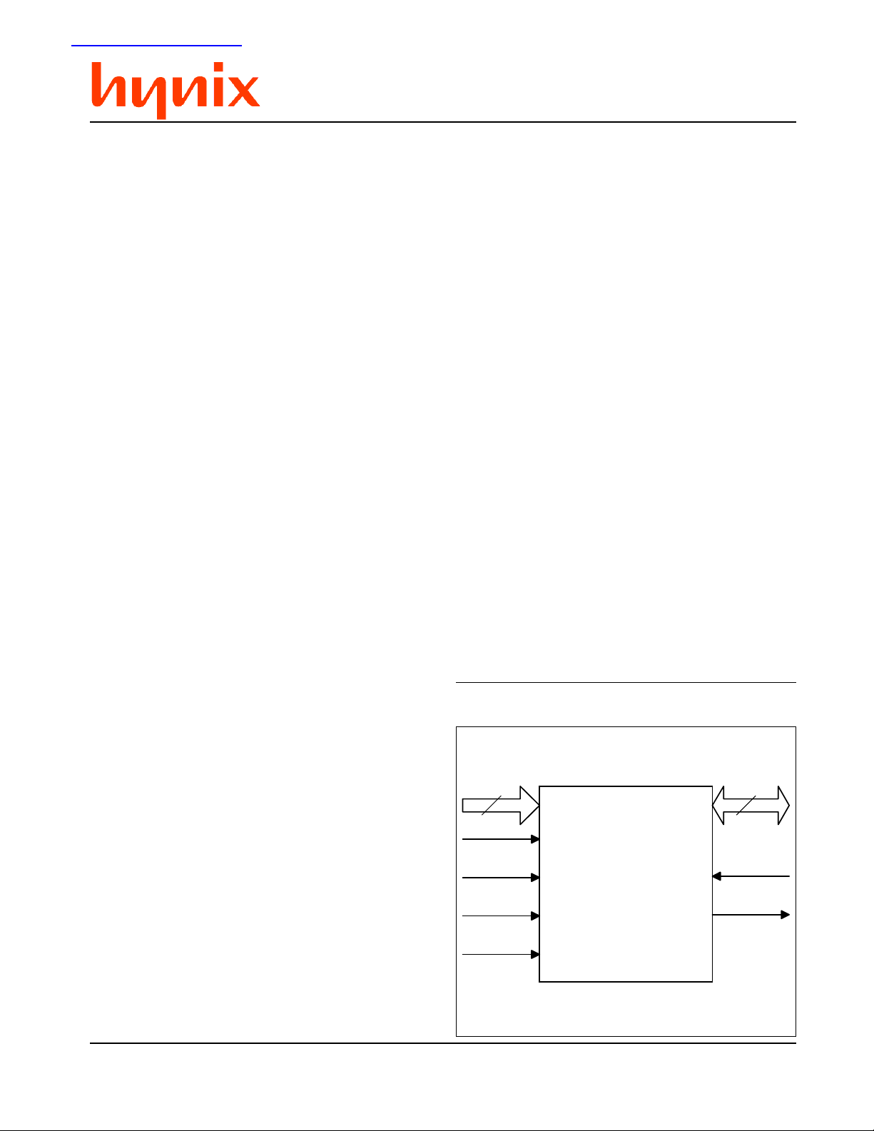
LOGIC DIAGRAM
21
A[20:0]
CE#
OE#
WE#
DQ[15:0]
WP#/ACC
RY/BY#
16
Revision 1.3, May 2002
RESET#
Page 2

HY29LV320
GENERAL DESCRIPTION
The HY29LV320 is a 32 Mbit, 3 volt-only CMOS
Flash memory organized as 2,097,152 (2M) words.
The device is available in 48-pin TSOP and 63ball FBGA packages. Word-wide data (x16) appears on DQ[15:0].
The HY29L V320 can be programmed and erased
in-system with a single 3 volt V
supply. Inter-
CC
nally generated and regulated voltages are provided for program and erase operations, so that
the device does not require a higher voltage V
PP
power supply to perform those functions. The device can also be programmed in standard EPROM
programmers. Access times as fast as 70ns over
the full operating voltage range of 2.7 - 3.6 volts
are offered for timing compatibility with the zero
wait state requirements of high speed microprocessors. To eliminate bus contention, the
HY29L V320 has separate chip enable (CE#), write
enable (WE#) and output enable (OE#) controls.
The device is compatible with the JEDEC singlepower-supply Flash command set standard. Commands are written to the command register using
standard microprocessor write timings, from where
they are routed to an internal state-machine that
controls the erase and programming circuits.
Device programming is performed a word at a time
by executing the four-cycle Program Command
write sequence. This initiates an internal algorithm
that automatically times the program pulse widths
and verifies proper cell margin. Faster programming times are achieved by placing the
HY29LV320 in the Unlock Bypass mode, which
requires only two write cycles to program data instead of four.
The HY29LV320 features a sector architecture and
is offered in two versions:
n HY29LV320B - a device with boot-sector archi-
tecture with the boot sectors at the bottom of the
address range, containing one 8KW, two 4KW,
one 16KW and sixty-three 32KW sectors.
n HY29LV320T - a device with boot-sector archi-
tecture with the boot sectors at the top of the
address range, containing one 8KW, two 4KW,
one 16KW and sixty-three 32KW sectors.
The HY29L V320’s sector erase architecture allows
any number of array sectors to be erased and reprogrammed without affecting the data contents
of other sectors. Device erasure is initiated by
executing the Erase Command sequence. This
initiates an internal algorithm that automatically
preprograms the array (if it is not already programmed) before executing the erase operation.
As during programming cycles, the device automatically times the erase pulse widths and verifies proper cell margin. Sectors are arranged into
designated groups for purposes of protection and
unprotection. Sector Group Protection optionally
disables both program and erase operations in any
combination of the sector groups of the memory
array, while Temporary Sector Group Unprotect
allows in-system erasure and code changes in
previously protected sector groups. Erase Suspend enables the user to put erase on hold for
any period of time to read data from, or program
data to, any sector that is not selected for erasure. True background erase can thus be
achieved. The device is fully erased when shipped
from the factory.
Addresses and data needed for the programming
and erase operations are internally latched during
write cycles, and the host system can detect
completion of a program or erase operation by
observing the RY/BY# pin, or by reading the DQ[7]
(Data# Polling) and DQ[6] (Toggle) status bits.
Hardware data protection measures include a low
V
detector that automatically inhibits write op-
CC
erations during power transitions.
After a program or erase cycle has been com-
pleted, or after assertion of the RESET# pin (which
terminates any operation in progress), the device
is ready to read data or to accept another command. Reading data out of the device is similar to
reading from other Flash or EPROM devices.
The Secured Sector is an extra 128 word sector
capable of being permanently locked at the factory or by customers. The Secured Indicator Bit
(accessed via the Electronic ID mode) is permanently set to a ‘1’ if the part is factory locked, and
permanently set to a ‘0’ if customer lockable. This
way, customer lockable parts can never be used
to replace a factory locked part. Factory locked
parts provide several options. The Secured Sector may store a secure, random 8-word ESN (Electronic Serial Number), customer code programmed at the factory, or both. Customer Lock-
2
r1.3/May 02
Page 3
HY29LV320
able parts may utilize the Secured Sector as bonus space, reading and writing like any other Flash
sector, or may permanently lock their own code
there.
The WP#/ACC pin provides two functions. The
Write Protect function provides a hardware method
of protecting the boot sectors without using a high
voltage. The Accelerate function speeds up programming operations, and is intended primarily to
allow faster manufacturing throughput.
Two power-saving features are embodied in the
HY29LV320. When addresses have been stable
for a specified amount of time, the device enters
the automatic sleep mode. The host can also place
the device into the standby mode. Power consumption is greatly reduced in both these modes.
Common Flash Memory Interface (CFI)
To make Flash memories interchangeable and to
encourage adoption of new Flash technologies,
major Flash memory suppliers developed a flexible method of identifying Flash memory sizes and
configurations in which all necessary Flash device
parameters are stored directly on the device.
Parameters stored include memory size, byte/word
configuration, sector configuration, necessary voltages and timing information. This allows one set
of software drivers to identify and use a variety of
different, current and future Flash products. The
standard which details the software interface necessary to access the device to identify it and to
determine its characteristics is the Common Flash
Memory Interface (CFI) Specification. The
HY29LV320 is fully compliant with this specification.
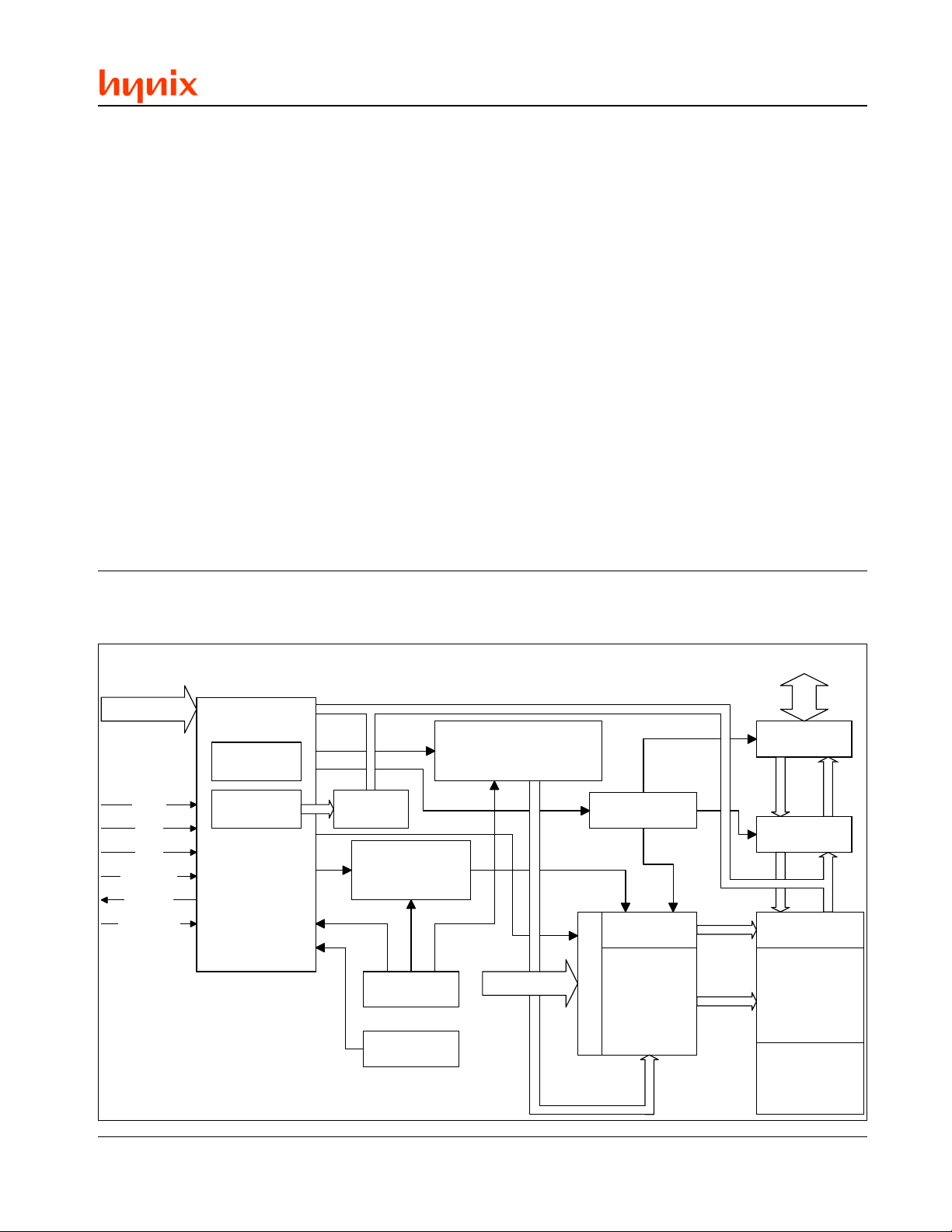
BLOCK DIAGRAM
A[20:0]
CONTROL
COMMAND
REGISTER
WE#
CE#
OE#
RESET#
RY/BY#
WP#/ACC
CONTROL
STATE
CFI
CFI DATA
MEMORY
PROGRAM
VOLTAGE
GENERATOR
TIMER
V
DETECTOR
ERASE VOLTAGE
GENERATOR AND
SECTOR SWITCHES
A[20:0]
CC
I/O CONTROL
Y-DECODER
X-DECODER
ADDRESS LATCH
DQ[15:0]
I/O BUFFERS
DATA LATCH
Y-GATING
32 Mb FLASH
MEMORY
ARRAY
(67 Sectors)
128-word
FLASH
Security Sector
r1.3/May 02
3
Page 4
HY29LV320
SIGNAL DESCRIPTIONS
emaN epyT noitpircseD
]0:02[AstupnI
]0:51[QD
#ECtupnI
#EOtupnI
#EWtupnI
#TESERtupnI
#YB/YR
CCA/#PWtupnI
V
HI
V
CC
V
SS
tupnI
--
--
.hgiHevitca,sserddA sdrow)M2(251,790,2foenotcelesstupni12esehT
.snoitarepoetirwrodaerrofyarraehtnihtiw
stuptuO/stupnI
etats-irT
hgiHevitca,suBataD dnadaerrofhtapatadtib-61aedivorpsnipesehT.
.snoitarepoetirw
.woLevitca,elbanEpihC romorfataddaerotdetressaebtsumtupnisihT
ehtdnadetats-irtsisubatadeht,hgiHnehW.023VL92YHehtotatadetirw
.edomybdnatSehtnidecalpsiecived
woLevitca,elbanEtuptuO snoitarepodaerrofdetressaebtsumtupnisihT.
eraecivedehtmorfstuptuoatad,hgiHnehW.snoitarepoetirwrofdetagendna
.etatsecnadepmihgihehtnidecalperasnipsubatadehtdnadelbasid
.woLevitca,elbanEetirW dnammocrosdnammocfognitirwslortnoC
nehwecalpsekatnoitarepoetirwA.snoitarepoecivedsuoiravrofsecneuqes
.hgiHsi#EOdnawoLoslasi#ECelihwdetressasi#EW
.woLevitca,teseRerawdraH ehtgnitteserfodohtemerawdrahasedivorP
yletaidemmiti,tesersiecivedehtnehW.etatsyarradaerehtot023VL92YH
etirw/daerlladnadetats-irtsisubatadehT.ssergorpninoitarepoynasetanimret
detressasi#TESERelihW.detressasitupniehtelihwderongierasdnammoc
.edomybdnatSehtnieblliwecivedeht
.sutatSysuB/ydaeR nisidnammocesareroetirwarehtehwsetacidnI
tuptuO
niarDnepO
#EWlanifehtfoegdegnisirehtretfadilaV.detelpmocneebsahrossergorp
ylevitcasiecivedehtelihwwoLsniameR.ecneuqesdnammocafoeslup
.atadyarradaerotydaersitinehwhgiHseogdna,gnisareroatadgnimmargorp
/woLevitca,tcetorPetirWV(etareleccA
VtanipsihtgnicalP
LI
.)
HH
mottobropotehtnisnoitarepoesarednamargorpselbasid
ehtrof3S-0SsrotceserasrotcesdetceffaehT.yarraehtfosdrowK23
.T023VL92YHehtrof66S-36SsrotcesdnaB023VL92YH
VtadecalpsinipehtfI
HI
otstreversrotcesowtesohtfoetatsnoitcetorpeht,
puorGrotceSehtgnisudetcetorpnurodetcetorpebottestsalerewyehtrehtehw
.023VL92YHehtfoytilibapacnoitcetorpnUdnanoitcetorP
VfI
HH
,edomssapyBkcolnUehtsretneecivedeht,tupnisihtotdeilppasi
ehtnoegatlovrehgihehtsesudna,srotcesdetcetorpynastcetorpnuyliraropmet
nehtdluowmetsysehT(.snoitarepomargorprofderiuqeremitehtecuderotnip
kcolnUehtybderiuqersaecneuqesdnammocmargorpelcyc-owtehtesu
VgnivomeR).edomssapyB
HH
lamronotecivedehtsnruternipehtmorf
.noitarepo
VtaebtontsumnipsihT
HH
,gnimmargorpdetareleccanahtrehtosnoitareporof
tluseryamdetcennocnurognitaolfnipehtgnivaeL.tluseryamegamadecivedro
.noitarepoecivedtnetsisnocnini
.tupnIhgiH VottcennoC
Votro
HI
CC
61x/8xralimishtiwytilibitapmocedivorpot
.secived
.ylppusrewop)lanimon(tlov-3
.dnuorglangisdnarewoP
4
r1.3/May 02
Page 5
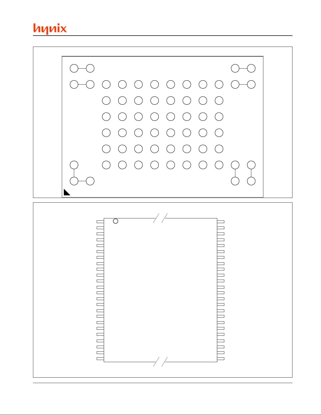
PIN CONFIGURATIONS
HY29LV320
63- B a ll l F B G A - T op Vp V ie w , B alls Facing D ow n
A8
NC
A7
NC
A2
NC
A1
NC
B8
NC
B7
NC
B1
NC
C7
A[13]D7A[12]E7A[14]F7A[15]G7A[16]H7V
C6
A[9]D6A[8]E6A[10]F6A[11]G6DQ[7]H6DQ[14]J6DQ[13]K6DQ[6]
C5
WE#D5RESET#E5NCF5A[19]G5DQ[5]H5DQ[12]J5V
C4
RY/BY#
C3
A[7]D3A[17]E3A[6]F3A[5]G3DQ[0]H3DQ[8]J3DQ[9]K3DQ[1]
C2
A[3]D2A[4]E2A[2]F2A[1]G2A[0]H2CE#J2OE#K2V
D4
WP#/ACC
E4
A[18]F4A[20]G4DQ[2]H4DQ[10]J4DQ[11]K4DQ[3]
10
J7
DQ[15]K7V
DQ[4]
++
K5
L8
M8
NC
NC
55
NC
55
NC
L7
L2
L1
NC
M7
NC
M2
NC
M1
NC
A[15]
A[14]
A[13]
A[12]
A[11]
A[10]
A[9]
A[8]
A[19]
A[20]910
WE#
RESET#1112
NC
WP#/ACC1314
RY/BY#
A[18]1516
A[17]
A[7]1718
A[6]
A[5]1920
A[4]
A[3]2122
A[2]
A[1]2324
1
2
3
4
5
6
7
8
TSOP48
48
47
46
45
44
43
42
41
40
39
38
37
36
35
34
33
32
31
30
29
28
27
26
25
A[16]
V
IH
V
SS
DQ[15]
DQ[7]
DQ[14]
DQ[6]
DQ[13]
DQ[5]
DQ[12]
DQ[4]
V
CC
DQ[11]
DQ[3]
DQ[10]
DQ[2]
DQ[9]
DQ[1]
DQ[8]
DQ[0]
OE#
V
SS
CE#
A[0]
r1.3/May 02
5
Page 6

HY29LV320
CONVENTIONS
Unless otherwise noted, a positive logic (active
High) convention is assumed throughout this document, whereby the presence at a pin of a higher,
more positive voltage (V
) causes assertion of the
IH
signal. A ‘#’ symbol following the signal name,
e.g., RESET#, indicates that the signal is asserted
in the Low state (V
V
and VIL values.
IH
). See DC specifications for
IL
MEMORY ARRA Y ORGANIZATION
The 32 Mbit Flash memory array is organized into
67 blocks called sectors (S0, S1, . . . , S66). A
sector or several contiguous sectors are defined
as a sector group. A sector is the smallest unit
that can be erased and a sector group is the smallest unit that can be protected to prevent accidental or unauthorized erasure.
In the HY29L V320, four of the sectors, which comprise the boot block, are sized as follows: one of
eight Kwords, two of four Kwords and one of
sixteen Kwords. The remaining 63 sectors are
sized at 32 Kwords. The boot block can be located at the bottom of the address range
(HY29L V320B) or at the top of the address range
(HY29LV320T).
Tables 1 and 2 define the sector addresses and
corresponding array address ranges for the top
and bottom boot block versions of the HY29L V320.
See Tables 6 and 7 for sector group definitions.
Secured Sector Flash Memory Region
The Secured Sector (Sec
2
) feature provides a 128
word Flash memory region that enables permanent part identification through an Electronic Serial Number (ESN). An associated ‘Sec
2
Indicator’ bit, which is permanently set at the factory and
cannot be changed, indicates whether or not the
2
Sec
is locked when shipped from the factory.
The device is offered with the Sec2 either factory
locked or customer lockable. The factory-locked
version is always protected when shipped from
the factory, and has the Sec
2
Indicator bit permanently set to a ‘1’. The customer-lockable version
is shipped with the Sec2 unprotected, allowing
customers to utilize the sector in any manner they
choose, and has the Sec
set to a ‘0’. Thus, the Sec
2
Indicator bit permanently
2
Indicator bit prevents
Whenever a signal is separated into numbered
bits, e.g., DQ[7], DQ[6], ..., DQ[0], the family of
bits may also be shown collectively, e.g., as
DQ[7:0].
The designation 0xNNNN (N = 0, 1, 2, . . . , 9, A, .
. . , E, F) indicates a number expressed in hexadecimal notation. The designation 0bXXXX indicates a
number expressed in binary notation (X = 0, 1).
customer-lockable devices from being used to replace devices that are factory locked. The bit prevents cloning of a factory locked part and thus
ensures the security of the ESN once the product
is shipped to the field.
The system accesses the Sec
2
through a command sequence (see “Enter/Exit Secured Sector
Command Sequence”). After the system has written the Enter Secured Sector command sequence,
it may read the Sec
2
by using the addresses specified in Table 3. This mode of operation continues
until the system issues the Exit Secured Sector
command sequence, or until power is removed
from the device. On power-up, or following a hardware reset, the device reverts to addressing the
Flash array.
Note: While in the Sec2 Read mode, only the reading of
the ‘Replaced Sector ’ (Table 3) is affected. Accesses
within the specified sector, but outside the address range
specified in the table, may produce indeterminate results.
Reading of all other sectors in the device continues normally while in this mode.
Sec2 Programmed and Protected At the Factory
In a factory-locked device, the Sec2 is protected
when the device is shipped from the factory and
cannot be modified in any way . The device is available preprogrammed with one of the following:
n A random, secure ESN only
n Customer code
n Both a random, secure ESN and customer
code
In devices that have an ESN, it will be located at
the bottom of the sector: starting at word address
0x000000 and ending at 0x000007 for a Bottom
Boot device, and starting at word address
0x1FE000 and ending at 0x1FE007 for a T op Boot
device. See Table 3.
6
r1.3/May 02
Page 7
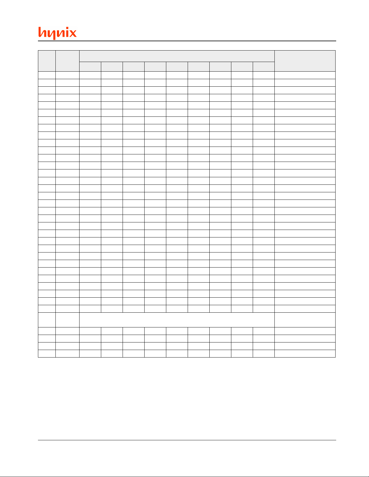
Table 1. HY29LV320T (Top Boot Block) Memory Array Organization
1
-tceS
ro
eziS
)droWK(
]02[A ]91[A ]81[A ]71[A ]61[A ]51[A ]41[A ]31[A ]21[A
0S23 000000XXX FFF700x0-000000x0
1S23 000001XXX FFFF00x0-000800x0
2S23 000010XXX FFF710x0-000010x0
3S23 000011XXX FFFF10x0-000810x0
4S23 000100XXX FFF720x0-000020x0
5S23 000101XXX FFFF20x0-000820x0
6S23 000110XXX FFF730x0-000030x0
7S23 000111XXX FFFF30x0-000830x0
8S23 001000XXX FFF740x0-000040x0
9S23 00 100 1XXX FFFF40x0-000840x0
01S23 001010XXX FFF750x0-000050x0
11S23 001011XXX FFFF50x0-000850x0
21S23 00 1100XXX FFF760x0-000060x0
31S23 00 1101XXX FFFF60x0-000860x0
41S23 001110XXX FFF770x0-000070x0
51S23 001111XXX FFFF70x0-000870x0
61S23 010000XXX FFF780x0-000080x0
71S23 010001XXX FFFF80x0-000880x0
81S23 0100 10XXX FFF790x0-000090x0
91S23 0100 11XXX FFFF90x0-000890x0
02S23 010100XXX FFF7A0x0-0000A0x0
12S23 0 10 101XXX FFFFA0x0-0008A0x0
22S23 010 110XXX FFF7B0x0-0000B0x0
32S23 010111XXX FFFFB0x0-0008B0x0
42S23 011000XXX FFF7C0x0-0000C0x0
52S23 011001XXX FFFFC0x0-0008C0x0
62S23 0110 10XXX FFF7D0x0-0000D0x0
72S23 0110 11XXX FFFFD0x0-0008D0x0
82S23 011100XXX FFF7E0x0-0000E0x0
92S23 011101XXX FFFFE0x0-0008E0x0
03S23 011110XXX FFF7F0x0-0000F0x0
13S23 011111XXX FFFFF0x0-0008F0x0
-23S
26S
231=]02[Atpecxe03S-0SsaemaS
36S61 1111110XX FFFBF1x0-0008F1x0
46S 4 111111100 FFFCF1x0-000CF1x0
56S 4 111111101 FFFDF1x0-000DF1x0
66S 8 11111111X FFFFF1x0-000EF1x0
Notes:
1. ‘X’ indicates don’t care.
2. ‘0xN. . . N’ indicates an address in hexadecimal notation.
3. The address range is A[20:0].
sserddArotceS
HY29LV320
3,2
egnaRsserddA
03S-0SsaemaS
1=DSMtpecxe
r1.3/May 02
7
Page 8
HY29LV320
Table 2. HY29LV320B (Bottom Boot Block) Memory Array Organization
1
-tceS
ro
0S800000000X FFF100x0-000000x0
1S4 000000010 FFF200x0-000200x0
2S4 000000011 FFF300x0-000300x0
3S61 0000001XX FFF700x0-000400x0
4S23 000001XXX FFFF00x0-000800x0
5S23 000010XXX FFF710x0-000010x0
6S23 000011XXX FFFF10x0-000810x0
7S23 000100XXX FFF720x0-000020x0
8S23 000101XXX FFFF20x0-000820x0
9S23 000110XXX FFF730x0-000030x0
01S23 000111XXX FFFF30x0-000830x0
11S23 001000XXX FFF740x0-000040x0
21S23 00 1001XXX FFFF40x0-000840x0
31S23 001010XXX FFF750x0-000050x0
41S23 001011XXX FFFF50x0-000850x0
51S23 00 1100XXX FFF760x0-000060x0
61S23 00 110 1XXX FFFF60x0-000860x0
71S23 001110XXX FFF770x0-000070x0
81S23 001111XXX FFFF70x0-000870x0
91S23 010000XXX FFF780x0-000080x0
02S23 010001XXX FFFF80x0-000880x0
12S23 0 10010XXX FFF790x0-000090x0
22S23 0100 11XXX FFFF90x0-000890x0
32S23 010100XXX FFF7A0x0-0000A0x0
42S23 010101XXX FFFFA0x0-0008A0x0
52S23 010 110XXX FFF7B0x0-0000B0x0
62S23 010111XXX FFFFB0x0-0008B0x0
72S23 011000XXX FFF7C0x0-0000C0x0
82S23 011001XXX FFFFC0x0-0008C0x0
92S23 0110 10XXX FFF7D0x0-0000D0x0
03S23 0110 11XXX FFFFD0x0-0008D0x0
13S23 011100XXX FFF7E0x0-0000E0x0
23S23 011101XXX FFFFE0x0-0008E0x0
33S23 011110XXX FFF7F0x0-0000F0x0
43S23 011111XXX FFFFF0x0-0008F0x0
53S23 100000XXX FFF701x0-000001x0
-63S
66S
Notes:
1. ‘X’ indicates don’t care.
2. ‘0xN. . . N’ indicates an address in hexadecimal notation.
3. The address range is A[20:0].
eziS
)droWK(
23
]02[A ]91[A ]81[A ]71[A ]61[A ]51[A ]41[A ]31[A ]21[A
sserddArotceS
1=]02[Atpecxe43S-4SsaemaS
3,2
egnaRsserddA
43S-4SsaemaS
1=DSMtpecxe
8
r1.3/May 02
Page 9

HY29LV320
Table 3. HY29LV320 Secure Sector Addressing
eciveD
T023VL92YH821)1elbaT(66SF70EF1x0-000EF1x0700EF1x0-000EF1x0
B023VL92YH821)2elbaT(0SF70000x0-000000x0700000x0-000000x0
Notes:
1. Accesses within the specified sector, but outside the specified address range, may produce indeterminate results.
2. ‘0xN. . . N’ indicates an address in hexadecimal notation. The address range is A[20:0].
eziSrotceS
)sdroW(
1
rotceSdecalpeR
2
egnaRsserddA
egnaRsserddA
rebmuNlaireScinortcelE
2
Sec2 NOT Programmed or Protected at the Factory
If the security feature is not required, the Sec2 can
be treated as an additional Flash memory space
of 128 words. The Sec
and erased as often as required. The Sec
2
can be read, programmed,
2
area
can be protected using the following procedure:
n Write the three-cycle Enter Secure Sector Re-
gion command sequence.
n Follow the in-system sector protect algorithm
as shown in Figure 3, except that RESET# may
be at either V
BUS OPERA TIONS
Device bus operations are initiated through the
internal command register, which consists of sets
of latches that store the commands, along with
the address and data information, if any, needed
to execute the specific command. The command
register itself does not occupy any addressable
memory location. The contents of the command
register serve as inputs to an internal state machine whose outputs control the operation of the
device.
Table 4 lists the normal bus operations, the inputs
and control levels they require, and the resulting
outputs. Certain bus operations require a high
voltage on one or more device pins. Those are
described in Table 5.
Data is read from the HY29LV320 by using standard microprocessor read cycles while placing the
word address on the device’s address inputs. The
host system must drive the CE# and OE# pins
LOW and drive WE# high for a valid read operation to take place. See Figure 1.
The HY29LV320 is automatically set for reading
array data after device power-up and after a hardware reset to ensure that no spurious alteration of
or VID. This allows in-system pro-
IH
tection of the Secure Sector without raising any
device pin to a high voltage. Note that this
method is only applicable to the Secure Sector.
n Once the Secure Sector is locked and verified,
the system must write the Exit Secure Sector
command sequence to return to reading and
writing the remainder of the array.
2
Sec
protection must be used with caution since,
once protected, there is no procedure available
for unprotecting the Sec
bits in the Sec
2
memory space can be modified in
any way .
the memory content occurs during the power transition. No command is necessary in this mode to
obtain array data, and the device remains enabled
for read accesses until the command register contents are altered.
This device features an Erase Suspend mode.
While in this mode, the host may read the array
data from any sector of memory that is not marked
for erasure. If the host reads from an address
within an erase-suspended (or erasing) sector, or
while the device is performing a program operation, the device outputs status data instead of array data. After completing an Automatic Program
or Erase algorithm within a sector, that sector automatically returns to the read array data mode.
After completing a programming operation in the
Erase Suspend mode, the system may once again
read array data with the same exception noted
above.
The host must issue a hardware reset or the software reset command to return a sector to the read
array data mode if DQ[5] goes high during a program or erase cycle, or to return the device to the
read array data mode while it is in the Electronic
ID mode.
2
area and none of the
r1.3/May 02
9
Page 10
HY29LV320
Table 4. HY29LV320 Normal Bus Operations
noitarepO #EC #EO #EW #TESER CCA/#PW ]0:02[A ]0:51[QD
1
daeRLLHHH/LA
NI
etirWLHLH3,2setoNANID
D
TUO
NI
elbasiDtuptuOLHHHH/LX Z-hgiH
ybdnatSlamroN#ECHXXHH/LX Z-hgiH
ybdnatSpeeD#ECV
V3.0±XXVCCV3.0±H/LX Z-hgiH
CC
)ybdnatSlamroN(teseRerawdraHXXXLH/LX Z-hgiH
)ybdnatSpeeD(teseRerawdraHXXXV
Notes:
1. L = V
2. If WP#/ACC = VIL, the boot sectors are protected. If WP#/ACC = VIH, the protection state of the boot sectors depends on
, H = VIH, X = Don’t Care (L or H), D
IL
= Data Out, DIN = Data In. See DC Characteristics for voltage levels.
OUT
whether they were last protected or unprotected using the method described in “Sector Group Protection and Unprotection”.
If WP#/ACC = V
3. See Table 5 for Accelerated Program function with WP#/ACC = V
, all sectors will be unprotected.
HH
HH
Table 5. HY29LV320 Bus Operations Requiring High Voltage
noitarepO #EC #EO #EW #TESER
margorPdetareleccALHLHV
tcetorPpuorGrotceSLHLV
tcetorpnUrotceSLHLV
rotceSyraropmeT
6
tcetorpnU
------V
DI
DI
DI
edoCrerutcafunaMLLHHH/LXV
eciveD
edoC
rotceS
tcetorP
4
etatS
eruceS
rotceS
rotacidnI
tiB
Notes:
1. L = VIL, H = VIH, X = Don’t Care (L or H), VID = 12V nominal. See DC Characteristics for voltage specifications.
2. Address bits not specified are Don’t Care.
3. SA = Sector Address, SGA = Sector Group Address. See Tables 1, 2, 6, and 7. A
4. If WP#/ACC = V
5. Protected sectors are temporarily unprotected when VHH is applied to the WP#/ACC pin.
6. Normal read, write and output disable operations are used in this mode. See Table 4.
7. D
= input data, CMDIN = Command input.
IN
B023VL92YH
LLH H H/LXVDILLH
T023VL92YH
detcetorpnU
LLH H H/LASV
detcetorP 10XXx0
yrotcaF
dekcoL
LLH H H/LXV
yrotcaFtoN
dekcoL
, the boot sectors remain protected.
IL
/#PW
CCA
5
HH
HAGSXLHLDMC
HXXHHLD
4etoN------------
V3.0±H/LX Z-hgiH
SS
.
1, 2
3
]21:02[A
A
NI
]9[A ]6[A ]1[A ]0[A ]0:51[QD
A
A
NI
DI
DI
DI
NI
LLL DA00x0
LHL
LHH
= address input.
IN
A
A
NI
NI
DMC
NI
NI
NI
D722x0
E722x0
00XXx0
08XXx0
00XXx0
7
10
r1.3/May 02
Page 11
WE#
WE#
ADR
ADR
CE#
CE#
OE#
OE#
DATA
DATA
OUT
OUT
t
t
ACC
ACC
t
t
CE
CE
t
t
OE
OE
Figure 1. Read Operation
Figure 1. Read Operation
Write Operation
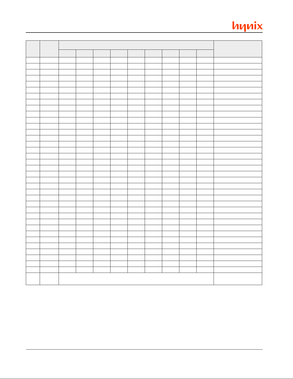
Certain operations, including programming data
and erasing sectors of memory, require the host
to write a command or command sequence to the
HY29LV320. Writes to the device are performed
by placing the word address on the device’s address inputs while the data to be written is input
on DQ[15:0]. The host system must drive the CE#
and WE# pins Low and drive OE# High for a valid
write operation to take place. All addresses are
latched on the falling edge of WE# or CE#, whichever happens later. All data is latched on the rising edge of WE# or CE#, whichever happens first.
See Figure 2.
.The “Device Commands ” section of this specification provides details on the specific device commands implemented in the HY29LV320.
HY29LV320
OE#
OE#
ADR
ADR
CE#
CE#
t
t
AH
AH
WE#
WE#
t
t
DS
DS
DATA
DATA
IN
IN
t
t
AS
AS
Figure 2. Write Operation
Figure 2. Write Operation
Note: WP# sector protection cannot be used while WP#/
ACC = VHH. Thus, all sectors are unprotected and can
be erased and programmed while in Accelerated Programming mode.
Note: The Accelerate function does not affect the time
required for Erase operations.
See the description of the WP#/ACC pin in the
Pin Descriptions table for additional information
on this function.
Write Protect Function
The Write Protect function provides a hardware
method of protecting the boot sectors without using V
. This function is a second function pro-
ID
vided by the WP#/ACC pin.
Placing this pin at V
disables program and erase
IL
operations in the bottom or top 32K words of the
array (the boot sectors). The affected sectors are
as follows (see Tables 1 and 2):
n HY29LV320B: S0 – S3
t
t
DH
DH
Accelerated Program Operation
This device offers accelerated program operations
through the “Accelerate” function provided by the
WP#/ACC pin. This function is intended primarily
for faster programming throughput at the factory.
If V
is applied to the WP#/ACC input, the device
HH
enters the Unlock Bypass mode, temporarily
unprotects any protected sectors, and uses the
higher voltage on the pin to reduce the time required for program operations. The system would
then use the two-cycle program command sequence as required by the Unlock Bypass mode.
Removing V
from the pin returns the device to
HH
normal operation.
r1.3/May 02
n HY29LV320T: S63 – S66
If the pin is placed at V
, the protection state of
IH
those sectors reverts to whether they were last
set to be protected or unprotected using the
method described in the Sector Group Protection
and Unprotection sections.
Note: Sectors protected by WP#/ACC = VIL remain pro-
tected during Temporary Sector Unprotect and cannot
be erased or programmed. Also see note under Accelerate Program Operation above.
Standby Operation
When the system is not reading or writing to the
device, it can place the device in the Standby
11
Page 12

HY29LV320
mode. In this mode, current consumption is greatly
reduced, and the data bus outputs are placed in
the high impedance state, independent of the OE#
input. The Standby mode can invoked using two
methods.
The device enters the CE# Controlled Deep
Standby mode when the CE# and RESET# pins
are both held at V
more restricted voltage range than V
CE# and RESET# are held at V
± 0.3V , the device will be in the Normal Standby
V
CC
± 0.3V. Note that this is a
CC
. If both
IH
, but not within
IH
mode, but the standby current will be greater.
Note: If the device is deselected during erasure or
programming, it continues to draw active current until
the operation is completed.
The device enters the RESET# Controlled Deep
Standby mode when the RESET# pin is held at
V
± 0.3V. If RESET# is held at VIL but not within
SS
V
± 0.3V , the standby current will be greater . See
SS
RESET# section for additional information on the
reset operation.
The device requires standard access time (t
CE
for read access when the device is in any of the
standby modes before it is ready to read data.
Sleep Mode
The sleep mode automatically minimizes device
power consumption. This mode is automatically
entered when addresses remain stable for t
ACC
+
30 ns (typical) and is independent of the state of
the CE#, WE#, and OE# control signals. Standard
address access timings provide new data when
addresses are changed. While in sleep mode,
output data is latched and always available to the
system. The device does not enter sleep mode if
an automatic program or automatic erase algorithm is in progress.
Output Disable Operation
When the OE# input is at V
, output data from
IH
the device is disabled and the data bus pins are
placed in the high impedance state.
Reset Operation
The RESET# pin provides a hardware method of
resetting the device to reading array data. When
the RESET# pin is driven low for the minimum
specified period, the device immediately terminates any operation in progress, tri-states the data
bus pins, and ignores all read/write commands for
the duration of the RESET# pulse. The device also
resets the internal state machine to reading array
data. If an operation was interrupted by the assertion of RESET#, it should be reinitiated once
the device is ready to accept another command
sequence to ensure data integrity.
Current is reduced for the duration of the RESET#
pulse as described in the Standby Operation section.
If RESET# is asserted during a program or erase
operation (RY/BY# pin is Low), the RY/BY# pin
remains Low (busy) until the internal reset operation is complete, which requires a time of t
(during Automatic Algorithms). The system can
thus monitor RY/BY# to determine when the reset
operation completes, and can perform a read or
write operation t
after RY/BY# goes High. If
RB
RESET# is asserted when a program or erase
operation is not executing (RY/BY# pin is High),
the reset operation is completed within a time of
t
. In this case, the host can perform a read or
RP
)
write operation t
after the RESET# pin returns
RH
High.
The RESET# pin may be tied to the system reset
signal. Thus, a system reset would also reset the
device, enabling the system to read the boot-up
firmware from the Flash memory.
Sector Group Protect Operation
The hardware sector group protection feature disables both program and erase operations in any
combination of sector groups. A sector group consists of a single sector or a group of adjacent sectors, as specified in Tables 6 and 7. This function
can be implemented either in-system or by using
programming equipment. It requires a high voltage (V
) on the RESET# pin and uses standard
ID
microprocessor bus cycle timing to implement
sector protection. The flow chart in Figure 3 illustrates the algorithm.
The HY29LV320 is shipped with all sectors unprotected. It is possible to determine whether a
sector is protected or unprotected. See the Electronic ID Mode section for details.
Sector Unprotect Operation
The hardware sector unprotection feature re-enables both program and erase operations in pre-
READY
12
r1.3/May 02
Page 13
HY29LV320
T able 6. Sector Groups - Top Boot Version T able 7. Sector Groups - Bottom Boot Version
puorG
0GS0S 000000XXX 23
1GS3S-1S
2GS7S-4S 000 1XXXXX 821
3GS11S-8S 00 10XXXXX 821
4GS51S-21S 00 11XXXXX 821
5GS91S-61S 0100XXXXX 821
6GS32S-02S 010 1XXXXX 821
7GS72S-42S 0110XXXXX 821
8GS13S-82S 0111XXXXX 821
9GS53S-23S 1000XXXXX 821
01GS93S-63S 100 1XXXXX 821
11GS34S-04S 1010XXXXX 821
21GS74S-44S 10 11XXXXX 821
31GS15S-84S 1100XXXXX 821
41GS55S-25S 110 1XXXXX 821
51GS95S-65S 1110XXXXX 821
61GS26S-06S
71GS36S 1111110XX 61
81GS46S 111111100 4
91GS56S 111111101 4
02GS66S 11111111X 8
srotceS
)1elbaT(
000001XXX
000011XXX
111100XXX
111110XXX
sserddApuorG
]21:02[A
eziSkcolB
)sdroWK(
69000010XXX
69111101XXX
puorG
0GS0S 00000000X 8
1GS1S 000000010 4
2GS2S 000000011 4
3GS3S 0000001XX 61
4GS6S-4S
5GS01S-7S 000 1XXXXX 821
6GS41S-11S 00 10XXXXX 821
7GS81S-51S 00 11XXXXX 821
8GS22S-91S 0100XXXXX 821
9GS62S-32S 010 1XXXXX 821
01GS03S-72S 0110XXXXX 821
11GS43S-13S 0111XXXXX 821
21GS83S-53S 1000XXXXX 821
31GS24S-93S 100 1XXXXX 821
41GS64S-34S 10 10XXXXX 821
51GS05S-74S 10 11XXXXX 821
61GS45S-15S 1100XXXXX 821
71GS85S-55S 110 1XXXXX 821
81GS26S-95S 1110XXXXX 821
91GS56S-36S
02GS66S 111111XXX 23
srotceS
)2elbaT(
000001XXX
000011XXX
111100XXX
111110XXX
sserddApuorG
]21:02[A
69000010XXX
69111101XXX
eziSkcolB
)sdroWK(
viously protected sector groups. This function can
be implemented either in-system or by using programming equipment. Note that to unprotect any
sector, all unprotected sector groups must first be
protected prior to the first sector unprotect write
cycle. Also, the unprotect procedure will cause
all sectors to become unprotected, thus, sector
groups that require protection must be protected
again after the unprotect procedure is run.
This procedure requires V
on the RESET# pin
ID
and uses standard microprocessor bus cycle timing to implement sector unprotection. The flow
chart in Figure 4 illustrates the algorithm.
Temporary Sector Unprotect Operation
This feature allows temporary unprotection of previously protected sector groups to allow changing
the data in-system. Temporary Sector Unprotect
mode is activated by setting the RESET# pin to
V
. While in this mode, formerly protected sec-
ID
r1.3/May 02
tors can be programmed or erased by invoking
the appropriate commands (see Device Commands section). Once V
is removed from RE-
ID
SET#, all the previously protected sector groups
are protected again. Figure 5 illustrates the algorithm.
NOTE: If WP#/ACC = VIL, the boot sectors remain pro-
tected.
Electronic ID Operation (High V oltage Method)
The Electronic ID mode provides manufacturer
and device identification, sector protection verification and Sec
2
region protection status through
identifier codes output on DQ[15:0]. This mode is
intended primarily for programming equipment to
automatically match a device to be programmed
with its corresponding programming algorithm.
Two methods are provided for accessing the Electronic ID data. The first requires V
on address
ID
pin A[9], with additional requirements for obtain-
13
Page 14
HY29LV320
START
RESET# = V
WP#/ACC = V
Wait 1 us
First Write Cycle:
Write 0x60 to device
TRYCNT = 1
Set Address:
A[20:12] = Address of Sector
Group to be Protected
A[6] = 0, A[1] = 1, A[0] = 0
Sector Group Protect:
Write 0x60 to Address
ID
IH
Wait 150 us
Verify Sector Group Protect:
Write 0x40 to Address
Read from Address
Data = 0x01?
YES
Protect Another
Sector Group?
YES
NO
NO
TRYCNT = 25?
NO
Increment TRYCNT
Figure 3. Sector Group Protect Algorithm
YES
RESET# = V
Write Reset Command
SECTOR GROUP
PROTECT COMPLETE
DEVICE FAILURE
IH
START
All sector groups
Note:
must be protected prior to
sector unprotection
TRYCNT = 1
SNUM = 0
RESET# = V
WP#/ACC = V
Wait 1 us
First Write Cycle:
Write 0x60 to device
Set Address:
A[6] = 1, A[1] = 1, A[0] = 0
Sector Unprotect:
Write 0x60 to Address
ID
IH
Set Address:
A[20:12] = Address of
Sector Group SNUM
A[6] = 1, A[1] = 1, A[0] = 0
Verify Unprotect:
Write 0x40 to Address
Read from Address
Data = 0x00?
YES
SNUM = 20?
NO
SNUM = SNUM + 1Wait 15 ms
NO
YES
TRYCNT = 1000?
NO
Increment TRYCNT
Figure 4. Sector Unprotect Algorithm
YES
RESET# = V
Write Reset Command
SECTOR UNPROTECT
COMPLETE
DEVICE FAILURE
IH
14
r1.3/May 02
Page 15

ing specific data items listed in T able 5. The Elec-
tronic ID data can also be obtained by the host
through specific commands issued via the command register, as described later in the ‘Device
Commands’ section of this data sheet.
While in the high-voltage Electronic ID mode, the
system may read at specific addresses to obtain
certain device identification and status information:
START
RESET# = V
(All protected sectors
become unprotected)
Perform Program or Erase
Operations
ID
HY29LV320
n A read cycle at address 0xXXX00 retrieves the
manufacturer code.
n A read cycle at address 0xXXX01 returns the
device code.
n A read cycle containing a sector address (SA)
in A[20:12] and the address 0x04 in A[7:0] returns 0x01 if that sector is protected, or 0x00 if
it is unprotected.
n A read cycle at address 0xXXX03 returns 0x80
if the Sec
the factory and 0x00 if it is not.
DEVICE COMMANDS
Device operations are initiated by writing designated address and data command sequences into
the device. Commands are routed to the command register for execution. This register is automatically selected as the destination for all write
operations and does not need to be explicitly addressed. Addresses are latched on the falling
edge of WE# or CE#, whichever happens later.
Data is latched on the rising edge of WE# or CE#,
whichever happens first.
A command sequence is composed of one, two
or three of the following sub-segments: an unlock
cycle, a command cycle and a data cycle. Table
8 summarizes the composition of the valid command sequences implemented in the HY29L V320,
and these sequences are fully described in Table
9 and in the sections that follow.
Writing incorrect address and data values or writing them in the improper sequence resets the device to the Read mode.
Reading Data
The device automatically enters the read array
mode after device power-up, after the RESET#
input is asserted and upon the completion of certain commands. Commands are not required to
2
region is protected and locked at
RESET# = V
(All previously protected
sectors return to protected
TEMPORARY SECTOR
UNPROTECT COMPLETE
IH
state)
Figure 5. Temporary Sector Unprotect
Algorithm
T able 8. Composition of Command Sequences
dnammoC
ecneuqeS
kcolnU dnammoC ataD
daeR001etoN
teseR010
2
ceSretnE
2
ceStixE
noigeR210
noigeR211
margorP211
ssapyBkcolnU210
ssapyBkcolnU
teseR
ssapyBkcolnU
margorP
01 1
01 1
esarEpihC411
esarErotceS41)2etoN(1
dnepsuSesarE010
emuseResarE010
DIcinortcelE213etoN
yreuQIFC014etoN
Notes:
1. Any number of Flash array read cycles are permitted.
2. Additional data cycles may follow. See text.
3. Any number of Electronic ID read cycles are permitted.
4. Any number of CFI data read cycles are permitted.
selcyCsuBforebmuN
r1.3/May 02
15
Page 16

HY29LV320
retrieve data in this mode. See Read Operation
section for additional information.
After the device accepts an Erase Suspend command, the HY29L V320 enters the erase-suspendread mode, after which the system can read data
from any non-erase-suspended sector . After completing a programming operation in the Erase
Suspend mode, the system may once again read
array data with the same exception. See the Erase
Suspend/Erase Resume Commands section for
more information.
Reset Command
Writing the Reset command resets the sectors to
the Read or Erase-Suspend mode. Address bits
are don’t cares for this command.
As described above, a Reset command is not normally required to begin reading array data. However, a Reset command must be issued in order
to read array data in the following cases:
n If the device is in the Electronic ID mode, a
Reset command must be written to return to
the Read array mode. If the device was in the
Erase Suspend mode when the device entered
the Electronic ID mode, writing the Reset command returns the device to the Erase Suspend
mode.
Note: When in the Electronic ID bus operation mode,
the device returns to the Read array mode when V
removed from the A[9] pin. The Reset command is not
required in this case.
is
ID
n If the device is in the CFI Query mode, a Reset
command must be written to return to the array Read mode.
n If DQ[5] (Exceeded T ime Limit) goes High dur-
ing a program or erase operation, a Reset command must be invoked to return the sectors to
the Read mode (or to the Erase Suspend mode
if the device was in Erase Suspend when the
Program command was issued).
The Reset command may also be used to abort
certain command sequences:
n In a Sector Erase or Chip Erase command se-
quence, the Reset command may be written
at any time before erasing actually begins, including, for the Sector Erase command, between the cycles that specify the sectors to be
erased (see Sector Erase command descrip-
tion). This aborts the command and resets the
device to the Read mode. Once erasure begins, however, the device ignores the Reset
command until the operation is complete.
n In a Program command sequence, the Reset
command may be written between the sequence cycles before programming actually begins. This aborts the command and resets the
device to the Read mode, or to the Erase Suspend mode if the Program command sequence
is written while the device is in the Erase Suspend mode. Once programming begins, however, the device ignores the Reset command
until the operation is complete.
n The Reset command may be written between
the cycles in an Electronic ID command sequence to abort that command. As described
above, once in the Electronic ID mode, the
Reset command must be written to return to
the array Read mode.
Note: The Reset command does not return the device
from Sec2 Region access to normal array access. See
descriptions of Enter/Exit Sec2 Region commands for
additional information.
Enter/Exit Sec2 Region Command Sequences
The system can access the Sec
device by issuing the Enter Sec
sequence. The device continues to access the
2
Sec
region until the system issues the Exit Sec
Region Command sequence, which returns the
device to normal operation.
Note that a hardware reset will reset the device to
the Read Array mode.
Program Command Sequence
The system programs the device a word at a time
by issuing the appropriate four-cycle Program
Command sequence as shown in Table 9. The
sequence begins by writing two unlock cycles, followed by the program setup command and, lastly ,
the program address and data. This initiates the
Automatic Program algorithm that automatically
provides internally generated program pulses and
verifies the programmed cell margin. The host is
not required to provide further controls or timings
during this operation. When the Automatic Program algorithm is complete, the device returns to
the reading array data mode. Several methods
are provided to allow the host to determine the
2
region of the
2
Region Command
2
16
r1.3/May 02
Page 17

HY29LV320
yrotcaftadekcoldnadetcetorpTON=00XX
yrotcaftadekcoldnadetcetorP=08XX
rotceSdetcetorpnU=00XX
rotceSdetcetorP=10XX
00
4,3,2,1
XXX
30XXX
selcyCsuB
02
09
555
55
89
tsriF dnoceS drihT htruoF htfiF htxiS
55XXX
1
3555AAAA2
etirW
ddA ataD ddA ataD ddA ataD ddA ataD ddA ataD ddA ataD
selcyC
1XXX0F
2XXX09XXX00
2XXX0AAPDP
1XXX0B
1XXX03
6555AAAA25555508555AAAA255AS03
ecneuqeSdnammoC
noigeR3555AAAA25555588
noigeR4555AAAA25555509
margorPlamroN4555AAAA2555550AAPDP
2
ceSretnE
2
ceStixE
7
teseR
daeR0ARDR
Table 9. HY29LV320 Command Sequences
r1.3/May 02
01
yreuQ)IFC(ecafretnIhsalFnommoC
tiBrotacidnInoigeR
5
margorPssapyBkcolnU
6
teseRssapyBkcolnU
ssapyBkcolnU3555AAAA255555
9
esarErotceS
esarEpihC6555AAAA25555508555AAAA25555501
edoCrerutcafunaM3555AAAA2555550900XXXDA00
7
8
dnepsuSesarE
emuseResarE
yfireVtcetorProtceS3555AAAA2555550920X)AS(
edoCeciveD3555AAAA2555550910XXXE722=tooBpoT,D722=tooBmottoB
2
ceS
11
Electronic ID
Legend:
X = Don’t Care RA/RD = Memory address/data for the read operation
PA/PD = Memory address/data for the program operation SA = A[20:12], sector address of the sector to be erased or verified (see Tables 1 and 2).
Notes:
1. All values are in hexadecimal.
2. All bus cycles are write operations except all cycles of the Read command and the fourth cycle of Electronic ID command.
3. Data bits DQ[15:8] are don’t cares except for ‘PD’ in program cycles.
4. Address is A[10:0]. Other (upper) address bits are don’t cares except when ‘SA’ or ‘PA’ is required.
5. The Unlock Bypass command is required prior to the Unlock Bypass Program command.
ID mode, while in the Erase Suspend mode.
8. The Erase Resume command is valid only during the Erase Suspend mode.
9. Multiple sectors may be specified for erasure. See command description.
10.See CFI section of specification for additional information.
6. The Unlock Bypass Reset command is valid only while the device is in the Unlock Bypass mode.
7. The Erase Suspend command is valid only during a sector erase operation. The system may read and program in non-erasing sectors, or enter the Electronic
11. See Electronic ID section of specification for additional information.
17
Page 18

HY29LV320
status of the programming operation, as described
in the Write Operation Status section.
Commands written to the device during execution
of the Automatic Program algorithm are ignored.
Note that a hardware reset immediately terminates
the programming operation (see Reset Operation
Timings). To ensure data integrity, the user should
reinitiate the aborted Program Command sequence after the reset operation is complete.
Programming is allowed in any sequence. Only
erase operations can convert a stored “0” to a “1”.
Thus, a bit cannot be programmed from a “0” back
to a “1”. Attempting to do so will cause the
HY29L V320 to halt the operation and set DQ[5] to
“1”, or cause the Data# Polling algorithm to indicate the operation was successful. However, a
succeeding read will show that the data is still “0”.
Figure 6 illustrates the programming operation.
Unlock Bypass Command Sequence
Unlock bypass provides a faster method than the
normal Program Command for the host system to
program the array. As shown in Table 9, the Unlock Bypass Command sequence consists of two
unlock write cycles followed by a third write cycle
containing the unlock bypass command, 0x20.
The device then enters Unlock Bypass mode. In
this mode, a two-cycle Unlock Bypass Program
Command sequence is used instead of the standard four-cycle sequence to invoke a programming operation. The first cycle in this sequence
contains the unlock bypass program command,
0xA0, and the second cycle specifies the program
address and data, thus eliminating the initial two
unlock cycles required in the standard Program
Command sequence. Additional data is programmed in the same manner. The unlock bypass mode does not affect normal read operations.
During the unlock bypass mode, only the Unlock
Bypass Program and the Unlock Bypass Reset
commands are valid. To exit the Unlock Bypass
mode, the host must issue the two-cycle Unlock
Bypass Reset command sequence shown in T able
9.
Figure 6 illustrates the procedures for the normal
and unlock bypass program operations.
The device automatically enters the unlock bypass
mode when it is placed in Accelerate mode via
the ACC pin.
Issue NORMAL PROGRAM
Command
Figure 6. Normal and Unlock Bypass Programming Procedures
START
NO
NO
Enable Fast
Programming?
YES
Issue UNLOCK BYPASS
Command
Setup Next Address/Data for
Program Operation
Unlock Bypass
Mode?
YES
Issue UNLOCK BYPASS
PROGRAM Command
Check Programming Status
(See Write Operation Status
Section)
Programming Verified
NO
Last Word/Byte
Done?
YES
NO
Unlock Bypass
Mode?
YES
Issue UNLOCK BYPASS
RESET Command
PROGRAMMING
COMPLETE
DQ[5] Error Exit
GO TO ERROR
RECOVERY PROCEDURE
18
r1.3/May 02
Page 19

HY29LV320
Chip Erase Command Sequence
The Chip Erase Command sequence consists of
two unlock cycles, followed by a set-up command,
two additional unlock cycles and then the Chip
Erase Command. This sequence invokes the
Automatic Chip Erase algorithm which automatically preprograms (if necessary) and verifies the
entire memory for an all zero data pattern before
electrical erase. The host system is not required
to provide any controls or timings during these
operations.
If all sectors in the device are protected, the device returns to reading array data after approximately 100 µs. If at least one sector is unprotected, the erase operation erases the unprotected
sectors, and ignores the command for the sectors
that are protected. Reads from the device during
operation of the Automatic Chip Erase Algorithm
return status data. See Write Operation Status
section of this specification.
Commands written to the device during execution
of the Automatic Chip Erase algorithm are ignored.
Note that a hardware reset immediately terminates
the chip erase operation (see Hardware Reset Timings). To ensure data integrity, the user should
reinitiate the aborted Chip Erase Command sequence after the reset operation is complete.
When the Automatic Chip Erase algorithm is complete, the device returns to the reading array data
mode. Several methods are provided to allow the
host to determine the status of the erase operation, as described in the Write Operation Status
section.
Figure 7 illustrates the chip erase procedure.
Sector Erase Command Sequence
The Sector Erase Command sequence consists
of two unlock cycles, followed by a set-up command, two additional unlock cycles and then the
Sector Erase Command, which specifies which
sector is to be erased. This sequence invokes
the Automatic Sector Erase algorithm which automatically preprograms (if necessary) and verifies
the specified sector for an all zero data pattern
before electrical erase. The host system is not
required to provide any controls or timings during
these operations.
After the sector erase command cycle (sixth cycle)
of the command sequence is issued, a sector
erase time-out of 50 µs (min) begins, measured
from the rising edge of the final WE# pulse in the
command sequence. During this time, an additional sector address and Sector Erase Command
may be written into an internal sector erase buffer .
This buffer may be loaded in any sequence, and
the number of sectors designated for erasure may
be from one sector to all sectors. The only restriction is that the time between these additional
cycles must be less than 50 µs, otherwise erasure may begin before the last address and command are accepted. T o ensure that all commands
are accepted, it is recommended that host processor interrupts be disabled during the time that
the additional sector erase commands are being
issued and then be re-enabled afterwards.
The system can monitor DQ[3] to determine if the
50 µs sector erase time-out has expired, as described in the Write Operation Status section. If
the time between additional sector erase commands can be assured to be less than the timeout, the system need not monitor the timeout.
START
Issue CHIP ERASE
Command Sequence
Check Erase Status
(See Write Operation Status
Section)
Normal Exit
CHIP ERASE COMPLETE
Figure 7. Chip Erase Procedure
r1.3/May 02
DQ[5] Error Exit
GO TO
ERROR RECOVERY
Note: Any command other than Sector Erase or Erase
Suspend during the time-out period resets the device to
reading array data. The system must then rewrite the
command sequence, including any additional sector
addresses and commands. Once the sector erase operation itself has begun, only the Erase Suspend command is valid. All other commands are ignored.
As for the chip erase command, note that a hardware reset immediately terminates the erase operation (see Hardware Reset Timings). To ensure
data integrity , the aborted sector erase command
sequence should be reissued once the reset operation is complete.
19
Page 20

HY29LV320
If all sectors designated for erasing are protected,
the device returns to reading array data after approximately 100 µs. If at least one designated
sector is unprotected, the erase operation erases
the unprotected sectors, and ignores the command
for the sectors that are protected. Read array
operations cannot take place until the Automatic
Erase algorithm terminates, or until the erase operation is suspended. Read operations while the
algorithm is in progress provide status data. When
the Automatic Erase algorithm is complete, the
device returns the erased sector(s) to the Read
(array data) mode.
Several methods are provided to allow the host to
determine the status of the erase operation, as
described in the Write Operation Status section.
Figure 8 illustrates the sector erase procedure.
Erase Suspend/Erase Resume Commands
The erase suspend command allows the system
to interrupt a sector erase operation to program
data into, or to read data from, any sector not
designated for erasure. The command causes
the erase operation to be suspended in all sectors designated for erasure. This command is valid
only during the sector erase operation, including
during the 50 µs time-out period at the end of the
command sequence, and is ignored if it is issued
during chip erase or programming operations.
The HY29LV320 requires a maximum of 20 µs to
suspend the erase operation if the erase suspend
command is issued during active sector erasure.
However, if the command is written during the
sector erase time-out, the time-out is terminated
and the erase operation is suspended immediately .
Once the erase operation has been suspended,
the system can read array data from or program
data into any sector that is not designated for erasure (protected sectors cannot be programmed).
Normal read and write timings and command definitions apply . Reading at any address within erasesuspended sectors produces status data on
DQ[7:0]. The host can use DQ[7], or DQ[6] and
DQ[2] together, to determine if a sector is actively
erasing or is erase-suspended. See “Write Operation Status” for information on these status bits.
After an erase-suspended program operation is
complete, the device returns to the erase-suspended read state and the host can initiate another programming operation (or read operation)
within non-suspended sectors. The host can determine the status of a program operation during
the erase-suspended state just as in the standard
programming operation.
START
Write First Five Cycles of
SECTOR ERASE
Command Sequence
Setup First (or Next) Sector
Address for Erase Operation
Write Last Cycle (SA/0x30)
of SECTOR ERASE
Command Sequence
Erase An
Additional Sector?
NO
20
YES
Check Erase Status
(See Write Operation Status
ERASE COMPLETE
Sectors that require erasure but
which were not specified in this
erase cycle must be erased later
using a new command sequence
NO
Sector Erase
Time-out (DQ[3])
Expired?
YES
Figure 8. Sector Erase Procedure
DQ[5] Error Exit
Section)
Normal Exit
GO TO
ERROR RECOVERY
r1.3/May 02
Page 21

HY29LV320
The host may also write the Electronic ID Command sequence when the chip is in the Erase
Suspend mode. The device allows reading Electronic ID codes even at addresses within erasing
sectors, since the codes are not stored in the
memory array. When the device exits the Electronic ID mode, the device reverts to the Erase
Suspend mode, and is ready for another valid
operation. See Electronic ID Mode section for
more information.
The system must write the Erase Resume command to exit the Erase Suspend mode and continue the sector erase operation. Further writes of
the Resume command are ignored. Another Erase
Suspend command can be written after the device has resumed erasing.
Note: If an erase operation is started while in the Sec
region and then suspended to do other operations, the
host must return the device to the Sec2 region before
issuing the Erase Resume command. Failure to do this
may result in the wrong sector being erased.
Electronic ID Command
n A read cycle at address 0xXXX00 retrieves the
manufacturer code.
n A read cycle at address 0xXXX01 in returns
the device code.
n A read cycle containing a sector address (SA)
in A[20:12] and the address 0x02 in A[7:0] returns 0x01 if that sector is protected, or 0x00 if
it is unprotected.
n A read cycle at address 0xXXX03 returns 0x80
if the Sec
the factory and returns 0x00 if it is not.
The system must write the Reset command to exit
the Electronic ID mode and return the bank to the
normal Read mode, or to the Erase-Suspended
read mode if the device was in that mode when
2
the Electronic ID command was invoked. In the
latter case, an Erase Resume command to that
bank will continue the suspended erase operation.
Query Command and Common Flash Interface (CFI) Mode
2
region is protected and locked at
The Electronic ID mode provides manufacturer
and device identification and sector protection verification through identifier codes output on
DQ[15:0]. This mode is intended primarily for programming equipment to automatically match a
device to be programmed with its corresponding
programming algorithm.
Two methods are provided for accessing the Electronic ID data. The first requires V
on address
ID
pin A[9], as described previously in the Device
Operations section.
The Electronic ID data can also be obtained by the
host through specific commands issued via the command register, as shown in Table 9. This method
does not require V
. The Electronic ID command
ID
sequence may be issued while the device is in the
Read mode or in the Erase Suspend Read mode.
The command may not be written while the device
is actively programming or erasing.
The Electronic ID command sequence is initiated
by writing two unlock cycles, followed by a third
write cycle that contains the Electronic ID command. The device then enters the Electronic ID
mode, and the system may read at any address
any number of times without initiating another command sequence.
The HY29LV320 is capable of operating in the
Common Flash Interface (CFI) mode. This mode
allows the host system to determine the manufacturer of the device, its operating parameters, its
configuration and any special command codes that
the device may accept. With this knowledge, the
system can optimize its use of the chip by using
appropriate timeout values, optimal voltages and
commands necessary to use the chip to its full
advantage.
Two commands are employed in association with
CFI mode. The first places the device in CFI mode
(Query command) and the second takes it out of
CFI mode (Reset command). These are described
in Table 10.
The single cycle Query command is valid only
when the device is in the Read mode, including
during Erase Suspend and Standby states and
while in Electronic ID command mode, but is ignored otherwise. The command is not valid while
the HY29L V320 is in the Electronic ID bus operation mode. Read cycles at appropriate addresses
while in the Query mode provide CFI data as described later in this section. Write cycles are ignored, except for the Reset command.
The Reset command returns the device from the
CFI mode to the array Read mode (even if it was
r1.3/May 02
21
Page 22

HY29LV320
in the Electronic ID mode when the Query command was issued), or to the Erase Suspend mode
if the device was in that mode prior to entering
CFI mode. The Reset command is valid only when
the device is in the CFI mode and as otherwise
described for the normal Reset command.
Table 10. CFI Mode: Identification Data Values
noitpircseD sserddA ataD
"YRQ"gnirtsIICSAeuqinu-yreuQ
elbatyreuqdednetxemhtiroglayramirprofsserddA
Tables 10 - 13 specify the data provided by the
HY29LV320 during CFI mode. Data at unspecified addresses reads out as 0x00. Note that a
value of 0x00 for a data item normally indicates
that the function is not supported. All values in
these tables are in hexadecimal notation.
01
11
21
edocDIecafretnilortnocdnatesdnammocrodnevyramirP
)enon(edocDIecafretnilortnocdnatesdnammocrodnevetanretlA
)enon(elbatyreuqdednetxemhtiroglayradnocesrofsserddA
31
41
51
61
71
81
91
A1
1500
2500
9500
2000
0000
0400
0000
0000
0000
0000
0000
22
r1.3/May 02
Page 23

Table 11. CFI Mode: System Interface Data Values
noitpircseD sserddA ataD
V
CC
V
CC
V
PP
V
PP
)V7.2(muminim,ylppus B17200
)V6.3(mumixam,ylppus C16300
)enon(muminim,ylppus D10000
)enon(mumixam,ylppus E10000
N
)sµF14000
2(etirwetyb/drowelgnisroftuoemitlacipyT
N
)sµ020000
2(etirwreffubezismumixamroftuoemitlacipyT
N
)sm129000
2(esarekcolblaudividniroftuoemitlacipyT
N
)sm22F000
2(esarepihcllufroftuoemitlacipyT
N
2(etirwetyb/drowelgnisroftuoemitmumixaM
2(esarekcolblaudividniroftuoemitmumixaM
)pyTx325000
N
2(etirwreffubezismumixamroftuoemitmumixaM
N
)pyTx420000
)pyTx524000
)detroppuston(esarepihcllufroftuoemitmumixaM 620000
Table 12. CFI Mode: Device Geometry Data Values
noitpircseD sserddA ataD
N
2(eziseciveD
)setyb726100
edocecafretniecivedhsalF
)61xsuonorhcnysa=10(
snoigerkcolbesareforebmuN C24000
noitamrofni1noigerkcolbesarE
1-noigerniskcolbfo#=]D2,E2[
setyb-652foselpitlumniezis=]F2,03[
noitamrofni2noigerkcolbesarE
noitamrofni3noigerkcolbesarE
noitamrofni4noigerkcolbesarE
HY29LV320
82
92
)detroppuston(etirwetyb-itlumnisetybforebmunmumixaM
A2
B2
D2
E2
F2
03
13
23
33
43
53
63
73
83
93
A3
B3
C3
1000
0000
0000
0000
0000
0000
0400
0000
1000
0000
0200
0000
0000
0000
0800
0000
E300
0000
0000
1000
r1.3/May 02
23
Page 24

HY29LV320
Table 13. CFI Mode: Vendor-Specific Extended Query Data Values
noitpircseD sserddA ataD
"IRP"gnirtsIICSAeuqinu-yreuQ
IICSA,rebmunnoisrevrojaM 341300
IICSA,rebmunnoisrevroniM 440300
kcolnuevitisnessserddA)deriuqerton=1,deriuqer=0(540000
)etirwdnadaerot=2(dnepsusesarE 642000
)puorg/srotcesfo#=N(tcetorprotceS 741000
tcetorpnurotcesyraropmeT)detroppus=1(841000
emehcstcetorpnu/tcetorprotceS)dohtemA008VL92mA=4(944000
noitarepoW/RsuoenatlumiS
)detroppuston=0:2knaBnisrotcesforebmun=xx(
)detroppuston=0(epytedomtsruB B40000
epytedomegaP)detroppuston=0(C40000
)V5.11(muminimylppuSCCA D45B00
)V5.21(mumixamylppuSCCA E45C00
)tooBpoT=BT,tooBmottoB=BB(noisrevtoobmottob/poT F4
WRITE OPERA TION ST A TUS
04
14
24
A40000
0500
2500
9400
)BB(2000
)BT(3000
The HY29L V320 provides a number of facilities to
determine the status of a program or erase operation. These are the RY/BY# (Ready/Busy#)
pin and certain bits of a status word which can be
read from the device during the programming and
erase operations. Table 11 summarizes the status indications and further detail is provided in the
subsections which follow.
RY/BY# - Ready/Busy#
RY/BY# is an open-drain output pin that indicates
whether a programming or erase Automatic Algorithm is in progress or has completed. A pull-up
resistor to V
is required for proper operation. RY/
CC
BY# is valid after the rising edge of the final WE#
pulse in the corresponding command sequence.
If the output is Low (busy), the device is actively
erasing or programming, including programming
while in the Erase Suspend mode. If the output is
High (ready), the device has completed the operation and is ready to read array data in the normal or
Erase Suspend modes, or it is in the Standby mode.
DQ[7] - Data# Polling
The Data# (“Data Bar”) Polling bit, DQ[7], indicates
to the host system whether an Automatic Algo-
rithm is in progress or completed, or whether the
device is in Erase Suspend mode. Data# Polling
is valid after the rising edge of the final WE# pulse
in the Program or Erase command sequence.
The system must do a read at the program address to obtain valid programming status information on this bit. While a programming operation is
in progress, the device outputs the complement
of the value programmed to DQ[7]. When the programming operation is complete, the device outputs the value programmed to DQ[7]. If a program operation is attempted within a protected
sector, Data# Polling on DQ[7] is active for approximately 1 µs, then the device returns to reading array data.
The host must read at an address within any nonprotected sector specified for erasure to obtain
valid erase status information on DQ[7]. During
an erase operation, Data# Polling produces a “0”
on DQ[7]. When the erase operation is complete,
or if the device enters the Erase Suspend mode,
Data# Polling produces a “1” on DQ[7]. If all sectors selected for erasing are protected, Data#
Polling on DQ[7] is active for approximately 100
µs, then the device returns to reading array data.
If at least one selected sector is not protected, the
erase operation erases the unprotected sectors,
24
r1.3/May 02
Page 25

HY29LV320
Table 14. Write and Erase Operation Status Summary
1
edoM noitarepO ]7[QD ]6[QD ]5[QD ]3[QD ]2[QD #YB/YR
ssergorpnignimmargorP#]7[QDelggoT1/0
lamroN
detelpmocesarE
rotces
esarE
dnepsuS
Notes:
1. A valid address is required when reading status information (except RY/BY#). For a programming operation, the address used for the read cycle should be the program address. For an erase operation, the address used for the read
cycle should be any address within a non-protected sector marked for erasure (any address within a non-protected
sector for the chip erase operation).
2. DQ[5] status switches to a ‘1’ when a program or erase operation exceeds the maximum timing limit.
3. A ‘1’ during sector erase indicates that the 50 µs time-out has expired and active erasure is in progress. DQ[3] is not
applicable to the chip erase operation.
4. Equivalent to ‘No Toggle’ because data is obtained in this state.
5. Data (DQ[7:0]) = 0xFF immediately after erasure.
6. Programming can be done only in a non-suspended sector (a sector not specified for erasure).
detelpmocgnimmargorPataDataD
ssergorpniesarE0elggoT1/0
5
dednepsusesarenihtiwdaeR
esare-nonnihtiwdaeR
rotcesdednepsus
6
ssergorpnignimmargorP
6
detelpmocgnimmargorP
ataDataD
1elggotoN0A/NelggoT1
ataDataDataDataDataD1
#]7[QDelggoT1/0
ataDataD
and ignores the command for the specified sectors that are protected.
When the system detects that DQ[7] has changed
from the complement to true data (or “0” to “1” for
erase), it should do an additional read cycle to read
valid data from DQ[7:0]. This is because DQ[7]
may change asynchronously with respect to the
other data bits while Output Enable (OE#) is asserted low.
Figure 9 illustrates the Data# Polling test algorithm.
DQ[6] - Toggle Bit I
Toggle Bit I on DQ[6] indicates whether an Automatic Program or Erase algorithm is in progress
or complete, or whether the device has entered
the Erase Suspend mode. T oggle Bit I may be read
4
4
4
a protected sector, DQ[6] toggles for approximately
1 µs after the program command sequence is written, then returns to reading array data.
While the Automatic Erase algorithm is operating,
successive read cycles at any address cause
DQ[6] to toggle. DQ[6] stops toggling when the
erase operation is complete or when the device is
placed in the Erase Suspend mode. The host may
use DQ[2] to determine which sectors are erasing
or erase-suspended (see below). After an Erase
command sequence is written, if all sectors selected for erasing are protected, DQ[6] toggles for
approximately 100 µs, then returns to reading array data. If at least one selected sector is not
protected, the Automatic Erase algorithm erases
the unprotected sectors, and ignores the selected
sectors that are protected.
2
A/NA/N0
ataDataDataD1
2
ataDataDataD
2
3
1
elggoT0
4
1
A/NA/N0
ataDataDataD1
at any address, and is valid after the rising edge
of the final WE# pulse in the Program or Erase
command sequence, including during the sector
erase time-out. The system may use either OE#
or CE# to control the read cycles.
Successive read cycles at any address during an
Automatic Program algorithm operation (including
programming while in Erase Suspend mode) cause
DQ[6] to toggle. DQ[6] stops toggling when the op-
DQ[2] - Toggle Bit II
Toggle Bit II, DQ[2], when used with DQ[6], indicates whether a particular sector is actively erasing or whether that sector is erase-suspended.
Toggle Bit II is valid after the rising edge of the
final WE# pulse in the command sequence. The
device toggles DQ[2] with each OE# or CE# read
cycle.
eration is complete. If a program address falls within
r1.3/May 02
25
Page 26

HY29LV320
START
the program or erase cycle was not successfully
completed. DQ[5] status is valid only while DQ[7]
limit. This is a failure condition that indicates that
Read DQ[7:0]
at Valid Address (Note 1)
DQ[7] = Data?
YES
Test for DQ[7] = 1?
for Erase Operation
or DQ[6] indicate that the Automatic Algorithm is
in progress.
The DQ[5] failure condition will also be signaled if
the host tries to program a ‘1’ to a location that is
previously programmed to ‘0’, since only an erase
operation can change a ‘0’ to a ‘1’.
NO
For both of these conditions, the host must issue
NO
Notes:
1. During programming , the program address. During sector erase , an
address within any non-protected sector specified for erasure. During
chip erase , an address within any non-protected sector.
2. Recheck DQ[7] since it may change asynchronously to DQ[5].
DQ[5] = 1?
YES
Read DQ[7:0]
at Valid Address (Note 1)
Test for DQ[7] = 1?
for Erase Operation
DQ[7] = Data?
(Note 2)
NO
PROGRAM/ERASE
EXCEEDED TIME ERROR
YES
PROGRAM/ERASE
COMPLETE
a Reset command to return the device to the Read
mode.
DQ[3] - Sector Erase Timer
After writing a Sector Erase command sequence,
the host may read DQ[3] to determine whether or
not an erase operation has begun. When the
sector erase time-out expires and the sector erase
operation commences, DQ[3] switches from a ‘0’
to a ‘1’. Refer to the “Sector Erase Command”
section for additional information. Note that the
sector erase timer does not apply to the Chip Erase
Figure 9. Data# Polling Test Algorithm
command.
Note: While DQ[5] indicates an error condition, no commands (except Reads) will be accepted by the device. If
the device receives a command while DQ[5] is high, the
first write cycle of that command will reset the error condition and the remaining write cycles of that command
sequence will be ignored
DQ[2] toggles when the host reads at addresses
within sectors that have been specified for erasure, but cannot distinguish whether the sector is
actively erasing or is erase-suspended. DQ[6],
by comparison, indicates whether the device is actively erasing or is in Erase Suspend, but cannot
distinguish which sectors are specified for erasure.
Thus, both status bits are required for sector and
mode information.
Figure 10 illustrates the operation of Toggle Bits I
and II.
DQ[5] - Exceeded Timing Limits
DQ[5] is set to a ‘1’ when the program or erase
time has exceeded a specified internal pulse count
26
After the initial Sector Erase command sequence
is issued, the system should read the status on
DQ[7] (Data# Polling) or DQ[6] (Toggle Bit I) to
ensure that the device has accepted the command
sequence, and then read DQ[3]. If DQ[3] is a ‘1’,
the internally controlled erase cycle has begun and
all further sector erase data cycles or commands
(other than Erase Suspend) are ignored until the
erase operation is complete. If DQ[3] is a ‘0’, the
device will accept a sector erase data cycle to mark
an additional sector for erasure. To ensure that
the data cycles have been accepted, the system
software should check the status of DQ[3] prior to
and following each subsequent sector erase data
cycle. If DQ[3] is high on the second status check,
the last data cycle might not have been accepted.
r1.3/May 02
Page 27

START
HY29LV320
Read DQ[7:0]
at Valid Address (Note 1)
Read DQ[7:0]
at Valid Address (Note 1)
DQ[6] Toggled?
NO
(Note 4)
NO
(Note 3)
PROGRAM/ERASE
COMPLETE
:
Notes
1. During programming, the program address.
During sector erase, an address within any sector scheduled for erasure.
2. Recheck DQ[6] since toggling may stop at the same time as DQ[5] changes from 0 to 1.
3. Use this path if testing for Program/Erase status.
4. Use this path to test whether sector is in Erase Suspend mode.
YES
NO
NO
DQ[5] = 1?
YES
Read DQ[7:0]
at Valid Address (Note 1)
DQ[6] Toggled?
(Note 2)
YES
PROGRAM/ERASE
EXCEEDED TIME ERROR
Read DQ[7:0]
Read DQ[7:0]
DQ[2] Toggled?
SECTOR BEING READ
IS IN ERASE SUSPEND
Figure 10. Toggle Bit I and II Test Algorithm
HARDWARE DA T A PROTECTION
The HY29L V320 provides several methods of protection to prevent accidental erasure or programming which might otherwise be caused by spurious system level signals during V
power-up and
CC
power-down transitions, or from system noise.
These methods are described in the sections that
follow.
Write Pulse “Glitch” Protection
Noise pulses of less than 5 ns (typical) on OE#,
CE# or WE# do not initiate a write cycle.
Logical Inhibit
Write cycles are inhibited by asserting any one of
the following conditions: OE# = V
Command Sequences
Commands that may alter array data require a
sequence of cycles as described in Table 9. This
provides data protection against inadvertent writes.
WE# = V
must be a logical zero while OE# is a logical one.
Power-Up Write Inhibit
. T o initiate a write cycle, CE# and WE#
IH
If WE# = CE# = V
Low V
To protect data during V
Write Inhibit
CC
power-up and power-
CC
down, the device does not accept write cycles
when V
is less than V
CC
(typically 2.4 volts). The
LKO
command register and all internal program/erase
circuits are disabled, and the device resets to the
Read mode. Writes are ignored until V
than V
. The system must provide the proper
LKO
is greater
CC
signals to the control pins to prevent unintentional
writes when V
is greater than V
CC
LKO
.
the device does not accept commands on the rising
edge of WE#. The internal state machine is automatically reset to the Read mode on power-up.
Sector Protection
Additional data protection is provided by the
HY29LV320’s sector protect feature, described
previously , which can be used to protect sensitive
areas of the Flash array from accidental or unauthorized attempts to alter the data.
NO
YES
SECTOR BEING READ
IS NOT IN ERASE SUSPEND
, CE# = VIH, or
IL
and OE# = VIH during power up,
IL
r1.3/May 02
27
Page 28

HY29LV320
ABSOLUTE MAXIMUM RA TINGS
4
lobmyS retemaraP eulaV tinU
T
GTS
T
SAIB
1
V
V
2NI
I
SO
CC
Notes:
1. Minimum DC voltage on input or I/O pins is –0.5 V. During voltage transitions, input or I/O pins may undershoot V
-2.0V for periods of up to 20 ns. See Figure 1 1. Maximum DC voltage on input or I/O pins is V
transitions, input or I/O pins may overshoot to V
2. Minimum DC input voltage on pins A[9], WP#/ACC, OE#, and RESET# is -0.5 V. During voltage transitions, A[9], WP#/
ACC, OE#, and RESET# may undershoot V
voltage on pins A[9], WP#/ACC, OE# and RESET# is +12.5 V which may overshoot to 14.0 V for periods up to 20 ns.
3. No more than one output at a time may be shorted to V
4. Stresses above those listed under “Absolute Maximum Ratings” may cause permanent damage to the device. This is a
stress rating only; functional operation of the device at these or any other conditions above those indicated in the
operational sections of this data sheet is not implied. Exposure of the device to absolute maximum rating conditions for
extended periods may affect device reliability.
RECOMMENDED OPERA TING CONDITIONS
erutarepmeTegarotS051+ot56-Cº
deilppArewoPhtiwerutarepmeTtneibmA521+ot56-Cº
VottcepseRhtiwniPnoegatloV
:
SS
0.4+ot5.0-
2
1
sniPrehtOllA
3
tnerruCtiucriCtrohStuptuO
+2.0 V for periods up to 20 ns. See Figure 12.
CC
to –2.0 V for periods of up to 20 ns. See Figure 11. Maximum DC input
SS
#TESER,CCA/#PW,#EO,]9[A
. Duration of the short circuit should be less than one second.
SS
1
5.21+ot5.0-
V(ot5.0-
)5.0+
CC
002Am
+ 0.5 V. During voltage
CC
V
V
V
to
SS
lobmyS retemaraP eulaV tinU
:erutarepmeTgnitarepOtneibmA
T
A
seciveDerutarepmeTlaicremmoC
seciveDerutarepmeTlairtsudnI
V
CC
Notes:
1. Recommended Operating Conditions define those limits between which the functionality of the device is guaranteed.
2. See Valid Combinations table, page 43.
egatloVylppuSgnitarepO2etoNV
20 ns 20 ns
0.8 V
VCC + 2.0 V
07+ot0
58+ot04-
20 ns
Cº
Cº
- 0.5 V
V
+ 0.5 V
CC
- 2.0 V
20 ns
2.0 V
20 ns 20 ns
Figure 11. Maximum Undershoot Waveform Figure 12. Maximum Overshoot Waveform
28
r1.3/May 02
Page 29

DC CHARACTERISTICS
retemaraP noitpircseD puteStseT
I
IL
I
TIL
I
OL
I
I
I
I
I
I
V
V
V
V
V
V
V
1CC
2CC
3CC
4CC
5CC
CCA
LI
HI
DI
HH
LO
1HO
CC
V
CC
V
CC
V
CC
,5
tnerruC
4
tnerruC
tnerruCdaoLtupnIV
tnerruCdaoLtupnI,]9[AV5.21=]9[A53Aµ
tnerruCegakaeLtuptuOV
1
tnerruCdaeRevitcA
4,3
tnerruCetirWevitcA
peeDdellortnoC#EC
tnerruCybdnatS
dellortnoC#TESER
tnerruCybdnatSpeeD
edoMpeelScitamotuA
margorPdetareleccA
egatloVwoLtupnI5.0-8.0V
egatloVhgiHtupnIx7.0V
dnaDIcinortcelErofegatloV
tcetorpnUrotceSyraropmeT
margorProfegatloV
noitareleccA
egatloVwoLtuptuO
egatloVhgiHtuptuO
V
2HO
V
OKL
VwoL
CC
Notes:
1. The I
2. All maximum current specifications are tested with VCC = VCC Max unless otherwise noted.
3. I
4. Not 100% tested.
current is listed is typically less than 2 mA/MHz with OE# at VIH. Typical VCC is 3.0 V.
CC
active while the Automatic Erase or Automatic Program algorithm is in progress.
CC
5. Automatic sleep mode is enabled when addresses remain stable for t
4
egatloVtuokcoL
NI
VHIV=
V
LI
V
CC
V
CC
V
CC
I
LO
V
CC
I
HO
V
CC
I
HO
V=
SS
V=
TUO
SS
V=#EC
,
LI
,
V=#EO
HI
V=#EC
,V=#EO
LI
V=#EC
CC
V=#TESER
Vro
SS
V=#TESER
Vro
SS
CC
V=
SS
V=#EC
LI
V=#EO
HI
V0.3=%01±5.115.21V
V0.3=%01±5.115.21V
V=
CC
Am0.4=
V=
CC
Am0.2-=
V=
CC
001-=Aµ
2
Vot
CC
Vot
CC
niM pyT xaM tinU
zHM5961Am
zHM124Am
HI
,V3.0±
CC
V=CCA/#PW
CC
,V3.0±
V3.0±
V3.0±
SS
V=CCA/#PW
,V3.0±
CC
V3.0±
V3.0±
,V3.0±
V3.0±
V
HH
V
CC
CC
,niM
,niM
,niM
Vx58.0
CC
V
4.0-V
CC
3.25.2V
+ 50 ns (typical).
ACC
HY29LV320
0.1±Aµ
0.1±Aµ
0203Am
5.05Aµ
5.05Aµ
5.05Aµ
501Am
5103Am
V
3.0+V
CC
54.0V
V
r1.3/May 02
29
Page 30

HY29LV320
DC CHARACTERISTICS
Zero Power Flash
20
15
10
Supply Current in mA
5
0
0 500 1000 1500 2000 2500 3000 3500 4000
Note: Addresses are switching at 1 MHz.
Time in ns
Figure 13. I
10
8
6
4
Supply Current in mA
2
0
123456
Note: TA = 25 °C.
Current vs. Time (Showing Active and Automatic Sleep Currents)
CC1
3.6 V
2.7 V
Frequency in MHz
Figure 14. Typical I
Current vs. Frequency
CC1
30
r1.3/May 02
Page 31

KEY TO SWITCHING WAVEFORMS
MROFEVAW STUPNI STUPTUO
HY29LV320
ydaetS
LotHmorfgnignahC
HotLmorfgnignahC
dettimrePegnahCynA,eraCt'noDnwonknUetatS,gnignahC
TEST CONDITIONS
DEVICE
UNDER
TEST
C
L
Figure 15. Test Setup
6.2
KOhm
+ 3.3V
2.7
KOhm
All diodes
are
1N3064
or
equivalent
ylppAtoNseoD
)ZhgiH(
Table 15. Test Specifications
tseT
noitidnoC
daoLtuptuOetaGLTT1
C(ecnaticapaCdaoLtuptuO
L
semiTllaFdnaesiRtupnI5sn
leveLwoLlangiStupnI0.0V
leveLhgiHlangiStupnI0.3V
tnemerusaeMgnimiTwoL
leveLlangiS
tnemerusaeMgnimiThgiH
leveLlangiS
Note: Timing measurements are made at the reference
levels specified above regardless of where the illustrations
in the timing diagrams appear to indicate the measurements
are made.
07-
)03001Fp
080921-
5.1V
5.1V
etatSecnadepmIhgiHsienilretneC
tinU
3.0 V
0.0 V
r1.3/May 02
I
nput
1.5 V
Measurement Level
Figure 16. Input Waveforms and Measurement Levels
1.5 V
Output
31
Page 32

HY29LV320
AC CHARACTERISTICS
Read Operations
retemaraP
CEDEJ dtS 07- 08- 09- 21-
t
t
t
t
t
t
t
t
VAVA
VQVA
VQLE
ZQHE
VQLG
ZQHG
XQXA
CR
t
CCA
t
EC
t
FD
t
EO
t
FD
t
HEO
t
HO
1
emiTdloH
Notes:
1. Not 100% tested.
2. See Figure 15 and Table 15 for test conditions.
1
emiTelcyCdaeR
elbanEtuptuO
noitpircseD puteStseT
yaleDtuptuOotsserddA
noitpOdeepS
niM070809021sn
V=#EC
LI
xaM070809021sn
LI
xaM070809021sn
LI
xaM52520303sn
xaM03035305sn
LI
xaM52030303sn
yaleDtuptuOotelbanEpihCV=#EO
1
ZhgiHtuptuOotelbanEpihC
yaleDtuptuOotelbanEtuptuOV=#EC
1
ZhgiHtuptuOotelbanEtuptuO
V=#EO
daeRniM0sn
dnaelggoT
gnilloP#ataD
#EC,sesserddAmorfemiTdloHtuptuO
1
tsriFsruccOrevehcihW,#EOro
niM01sn
niM0sn
tinU
Addresses
CE#
OE#
WE#
Outputs
RESET#
t
OEH
t
RC
Addresses Stable
t
ACC
t
OE
t
CE
t
OH
Output Valid
t
DF
32
RY/BY#
0 V
Figure 17. Read Operation Timings
r1.3/May 02
Page 33

AC CHARACTERISTICS
Hardware Reset (RESET#)
retemaraP
CEDEJ dtS 07- 08- 09- 21-
t
YDAER
t
YDAER
t
PR
t
HR
t
DPR
t
BR
Notes:
1. Not 100% tested.
2. See Figure 15 and Table 15 for test conditions.
noitpircseD puteStseT
htdiWesluP#TESERniM005sn
emiTyrevoceR#YB/YRniM0sn
HY29LV320
noitpOdeepS
citamotuAgniruD(woLniP#TESER
1
etirWrodaeRot)smhtiroglA
citamotuAgniruDTON(woLniP#TESER
1
etirWrodaeRot)smhtiroglA
1
daeRerofeBemiThgiH#TESER
edoMybdnatSotwoL#TESERxaM02sµ
xaM02sµ
xaM005sn
niM05sn
tinU
RY/BY#
CE#, OE#
RESET#
RY/BY#
CE#, OE#
RESET#
0 V
t
RH
t
RP
t
Ready
Reset Timings NOT During Automatic Algorithms
t
Ready
t
t
RP
RB
r1.3/May 02
Reset Timings During Automatic Algorithms
Figure 18. RESET# Timings
33
Page 34

HY29LV320
AC CHARACTERISTICS
Program and Erase Operations
retemaraP
CEDEJ dtS 07- 08- 09- 21-
t
t
t
t
t
t
t
t
t
t
t
t
t
t
t
VAVA
LWVA
XALW
HWVD
XDHW
LWHG
LWLE
HEHW
HWLW
LWHW
1HWHW
1HWHW
2HWHW
3HWHW
CW
t
SA
t
HA
t
TSA
t
THA
t
HPEC
t
HPEO
t
SD
t
HD
t
LWHG
t
SC
t
HC
t
PW
t
HPW
t
1HWHW
t
1HWHW
t
2HWHW
t
3HWHW
V
t
SCV
CC
V
t
HHV
HH
t
BR
t
YSUB
1
emiTelcyCetirW
emiTputeSsserddAniM0sn
emiTdloHsserddAniM54545405sn
tseTtiBelggoT
tseTtiBelggoT
emiTputeSataDniM54545405sn
emiTdloHataDniM0 sn
emiTputeS#ECniM0 sn
emiTdloH#ECniM0 sn
htdiWesluPetirWniM53535305sn
hgiHhtdiWesluPetirWniM03sn
noitarepOesarErotceS
noitarepOesarEpihC
1
emiTputeS
1
emiTllaFdnaesiR
noitpircseD
niM070809021sn
rofwoL#ECro#EOotemiTputeSsserddA
rofhgiH#ECro#EOmorfemiTdloHsserddA
niM51sn
niM0 sn
tseTtiBelggoTrofemiThgiHelbanEpihCniM02sn
tseTtiBelggoTrofemiThgiHelbanEtuptuOniM02sn
etirWerofeBemiTyrevoceRdaeRniM0sn
3,2,1
noitarepOgnimmargorPdroW
5,3,2,1
noitarepOgnimmargorPpihC
3,2,1
noitarepOgnimmargorPdroWdetareleccA
4,2,1
pyT11sµ
xaM003sµ
pyT32ces
xaM07ces
pyT7sµ
xaM012sµ
pyT5.0ces
xaM5.7ces
4,2,1
1
ecnarudnEelcyCmargorPdnaesarE
pyT23ces
niM000,001selcyc
pyT000,000,1selcyc
niM05sµ
niM052sn
#YB/YRmorfemiTyrevoceRniM0 sn
yaleD#YB/YRothgiH#EWniM09sn
Notes:
1. Not 100% tested.
2. Typical program and erase times assume the following conditions: 25 °C, V
programming typicals assume a checkerboard pattern. Maximum program and erase times are under worst case condi-
= 3.0 volts, 100,000 cycles. In addition,
CC
tions of 90 °C, VCC = 2.7 volts (3.0 volts for - 70 version), 100,000 cycles.
3. Excludes system-level overhead, which is the time required to execute the four-bus-cycle sequence for the program
command. See Table 9 for further information on command sequences.
4. Excludes 0x00 programming prior to erasure. In the preprogramming step of the Automatic Erase algorithm, all bytes
are programmed to 0x00 before erasure.
5. The typical chip programming time is considerably less than the maximum chip programming time listed since most
words program faster than the maximum programming times specified. The device sets DQ[5] = 1 only If the maximum
word program time specified is exceeded. See Write Operation Status section for additional information.
noitpOdeepS
tinU
34
r1.3/May 02
Page 35

HY29LV320
Program Command Sequence (last two cycles) Read Status Data (last two cycles)
Addresses
CE#
OE#
WE#
Data
RY/BY#
V
CC
t
VCS
t
WC
t
AS
0x555 PA PA PA
t
GHWL
t
CH
t
WP
t
CS
t
DS
t
WPH
t
DH
0xA0 PD Status
t
AH
t
BUSY
t
WHWH1
D
OUT
t
RB
Notes:
1. PA = Program Address, PD = Program Data, D
2. VCC shown only to illustrate t
measurement references. It cannot occur as shown during a valid command sequence.
VCS
Figure 19. Program Operation Timings
V
HH
ACC
VIL or V
IH
t
VHH
Figure 20. Accelerated Programming Voltage Timings
r1.3/May 02
is the true data at the program address.
OUT
t
VHH
VIL or V
IH
35
Page 36

HY29LV320
AC CHARACTERISTICS
Erase Command Sequence (last two cycles) Read Status Data (last two cycles)
Addresses
CE#
OE#
WE#
Data
RY/BY#
V
CC
t
VCS
t
WC
t
AS
0x2AA VA VA SA
t
GHWL
t
CH
t
WP
t
CS
t
DS
t
WPH
t
DH
0x55 0x30 Status D
t
AH
Address = 0x555
for chip erase
Data = 0x10
for chip erase
t
BUSY
t
WHWH2
t
WHWH3
or
OUT
t
RB
Notes:
1. SA =Sector Address (for sector erase), VA = Valid Address for reading status data (see Write Operation Status section),
D
is the true data at the read address.(0xFF after an erase operation).
OUT
2. V
shown only to illustrate t
CC
measurement references. It cannot occur as shown during a valid command sequence.
VCS
Figure 21. Sector/Chip Erase Operation Timings
36
r1.3/May 02
Page 37

AC CHARACTERISTICS
Addresses
t
RC
VA VA VA
HY29LV320
t
CH
t
ACC
CE#
t
CE
OE#
t
DF
t
OH
Complement Complement True Valid Data
Status Data Status Data Data Valid Data
WE#
DQ[7]
DQ[6:0]
t
BUSY
t
OEH
t
OE
RY/BY#
Notes:
1. VA = Valid Address for reading Data# Polling status data (see Write Operation Status section).
2. Illustration shows first status cycle after command sequence, last status read cycle and array data read cycle.
Figure 22. Data# Polling Timings (During Automatic Algorithms)
t
ACC
t
RC
Addresses
CE#
OE#
t
AST
t
OEH
t
CH
VA VA VA
t
AHT
t
CE
t
t
OE
CEPH
t
OEPH
t
DF
VA
WE#
t
OH
DQ[6], [2]
t
BUSY
Valid Status Valid Status Valid Status
(second read)(first read) (stops toggling)
Valid Data
RY/BY#
Notes:
1. VA = Valid Address for reading Toggle Bits (DQ[2], DQ[6]) status data (see Write Operation Status section).
2. Illustration shows first two status read cycles after command sequence, last status read cycle and array data read cycle.
Figure 23. Toggle Bit Timings (During Automatic Algorithms)
r1.3/May 02
37
Page 38

HY29LV320
AC CHARACTERISTICS
Enter Erase
Suspend
Program
Erase
Suspend
Program
Erase
Resume
Erase
Suspend
Read
Erase
Erase
Complete
WE#
Enter Automatic
Erase
Erase
Erase
Suspend
Erase
Suspend
Read
DQ[6]
DQ[2]
Notes:
1. The system may use CE# or OE# to toggle DQ[2] and DQ[6]. DQ[2] toggles only when read at an address within an
erase-suspended sector.
Figure 24. DQ[2] and DQ[6] Operation
Sector Protect and Unprotect, Temporary Sector Unprotect
retemaraP
CEDEJ dtS 07- 08- 09- 21-
t
RDIV
t
PSR
t
TSRV
t
TORP
t
RPNU
Notes:
1. Not 100% tested.
V
ID
RESET#
0 or 3V
t
VIDR
CE#
WE#
noitpircseD
V
DI
1
tcetorpnUrotceSyraropmeTrofemiTnoitisnarT
niM005sn
noitpOdeepS
tinU
tcetorpnUrotceSyraropmeTrofemiTputeS#TESERniM4 sµ
dnatcetorPpuorGrotceSrofemiTputeS#TESER
tcetorpnUrotceS
niM1sµ
emiTtcetorPpuorGrotceSxaM051sµ
emiTtcetorpnUrotceSxaM51sm
0 or 3V
t
VIDR
t
RSP
RY/BY#
38
Figure 25. Temporary Sector Unprotect Timings
r1.3/May 02
Page 39

AC CHARACTERISTICS
V
ID
V
RESET#
IH
HY29LV320
SGA, A[6],
A[1], A[0]
Data
Don't Care Valid * Valid * Valid *
Sector Group Protect/
Sector Unprotect
0x60 0x60 0x40 Status
t
t
VRST
PROT
or t
UNPR
Verify
CE#
WE#
OE#
Note: For Sector Group Protect, A[6] = 0, A[1] = 1, A[0] = 0. For Sector Unprotect, A[6] = 1, A[1] = 1, A[0] = 0.
Figure 26. Sector Group Protect and Sector Unprotect Timings
AC CHARACTERISTICS
Alternate CE# Controlled Erase/Program Operations
retemaraP
CEDEJ dtS 07- 08- 09- 21-
t
t
t
t
t
t
t
t
t
t
t
VAVA
LEVA
XALE
HEVD
XDHE
LEHG
LELW
HWHE
HELE
LEHE
CW
t
SA
t
HA
t
SD
t
HD
t
LEHG
t
SW
t
HW
t
PC
t
HPC
t
YSUB
1
emiTelcyCetirW
emiTputeSsserddAniM0 sn
emiTdloHsserddAniM54545405sn
emiTputeSataDniM54545405sn
emiTdloHataDniM0 sn
)woL#ECothgiH#EO(
emiTputeS#EWniM0 sn
emiTdloH#EWniM0 sn
htdiWesluP#ECniM53535305sn
hgiHhtdiWesluP#ECniM03sn
noitpircseD
niM070809021sn
etirWerofeBemiTyrevoceRdaeR
niM0 sn
yaleD#YB/YRothgiH#ECniM09sn
Notes:
1. Not 100% tested.
2. See Programming and Erase Operations table for Erase, Program and Endurance characterisitics.
noitpOdeepS
tinU
r1.3/May 02
39
Page 40

HY29LV320
AC CHARACTERISTICS
Addresses
WE#
OE#
CE#
Data
RY/BY#
RESET#
0x555 for Program
0x2AA for Erase
t
WC
t
GHEL
t
WS
t
DS
t
RH
SA for Sector Erase
0x555 for Chip Erase
t
t
WH
t
CP
0xA0 for Program
0x55 for Erase
t
CPH
t
DH
PA for Program
AS
t
AH
PD for Program
0x30 for Sector Erase
0x10 for Chip Erase
t
WHWH1
or t
t
BUSY
WHWH2
or t
WHWH3
Status D
VA
OUT
Notes:
1. PA = program address, PD = program data, VA = Valid Address for reading program or erase status (see Write
Operation Status section), D
= array data read at VA.
OUT
2. Illustration shows the last two cycles of the program or erase command sequence and the last status read cycle.
3. RESET# shown only to illustrate t
sequence.
measurement references. It cannot occur as shown during a valid command
RH
Figure 27. Alternate CE# Controlled Write Operation Timings
40
r1.3/May 02
Page 41

Latchup Characteristics
noitpircseD muminiM mumixaM tinU
VottcepserhtiwegatlovtupnI
SS
snipO/Itpecxesnipllano
)#TESERdna#EO,]9[A,CCA/#PWgnidulcni(
VottcepserhtiwegatlovtupnI
SS
V
CC
tnerruC001-001Am
Notes:
1. Includes all pins except VCC. Test conditions: VCC = 3.0V, one pin at a time.
snipO/Illano0.1-V
TSOP Pin Capacitance
lobmyS retemaraP puteStseT pyT xaM tinU
C
NI
C
TUO
C
2NI
Notes:
1. Sampled, not 100% tested.
2. Test conditions: T
= 25 ºC, f = 1.0 MHz.
A
ecnaticapaCtupnIV
ecnaticapaCtuptuOV
ecnaticapaCniPlortnoCV
0=65.7Fp
NI
0=5.821Fp
TUO
0=5.79 Fp
NI
Data Retention
retemaraP snoitidnoCtseT muminiM tinU
emiTnoitneteRataDnrettaPmuminiM
HY29LV320
0.1-5.21V
0.1+V
CC
Cº05101sraeY
Cº52102sraeY
P ACKAGE DRAWINGS
Physical Dimensions
TSOP48 - 48-pin Thin Small Outline Package (measurements in millimeters)
0.95
1.05
Pin 1 ID
1.20
MAX
1
24
0.25MM (0.0098") BSC
18.30
18.50
19.80
20.20
o
0
o
5
48
11.90
12.10
25
0.08
0.20
0.10
0.21
0.50 BSC
0.05
0.15
r1.3/May 02
0.50
0.70
41
Page 42

HY29LV320
P ACKAGE DRAWINGS
Physical Dimensions
FBGA63 - 63-Ball Fine-Pitch Ball Grid Array, 7.0 x 11 mm (measurements in millimeters)
0.10
C
Note: Unless otherwise specified, tolerance = ± 0.05
(4 x )
1.20
MAX
11.00 ?0.1
1.60
?0.10
A 1 C O R N E R
INDE X A R E A
2.80 ?0.10
+
B
7.0 ?0.1
A
+
0.1
C
0
Seating
Plane
C0.1
0.35
?0.05
0.74
?0.06
C
8.80 B SC
42
A
IJKL
8
7
6
5
+
4
3
2
1
0.45 ?0.05¨ª
?0.15 MC A B
?0.08 MC
+
BCDEFGH
5.60 B SC
0.80
TYP
Pin A 1
In d e x M a r k
r1.3/May 02
Page 43

HY29LV320
ORDERING INFORMATION
Hynix products are available in several speeds, packages and operating temperature ranges. The
ordering part number is formed by combining a number of fields, as indicated below. Refer to the ‘Valid
Combinations’ table, which lists the configurations that are planned to be supported in volume. Please
contact your local Hynix representative or distributor to confirm current availability of specific configurations and to determine if additional configurations have been released.
023VL92YH XX-XXX
SNOITCURTSNILAICEPS
EGNARERUTAREPMET
=knalB
=I
NOITPODEEPS
=07
=08
=09
=21
sn07
sn08
sn09
sn021
)C°07+ot0(laicremmoC
)C°58+ot04-(lairtsudnI
EPYTEGAKCAP
=T
=F
=T
=B
REBMUNECIVED
=023VL92YHesarErotceSylnO-tloV3SOMC)61xM2(tibageM23
NOITACOLKCOLBTOOB
noitpOkcolBtooBpoT
noitpOkcolBtooBmottoB
yromeMhsalF
)POST(egakcaPeniltuOllamSnihTniP-84
mm11x0.7,)AGBF(yarrAdirGllaBhctiP-eniFllaB-36
V ALID COMBINA TIONS
deepSdnaegakcaP
AGBF POST
erutarepmeT sn07 sn08 sn09 sn021 sn07 sn08 sn09 sn021
stloV6.3-7.2:egatloVgnitarepO
laicremmoC--08-F09-F21-F--08-T09-T21-T
lairtsudnII07-FI08-FI09-FI21-FI07-TI08-TI09-TI21-T
stloV6.3-0.3:egatloVgnitarepO
laicremmoC07-F------07-T------
Note:
1. The complete part number is formed by appending the suffix shown in the table to the Device Number. For example, the
part number for a 90 ns, Industrial temperature range device in the TSOP package with the top boot block option is
HY29LV320TT-90I.
r1.3/May 02
43
Page 44

HY29LV320
Important Notice
© 2001 by Hynix Semiconductor America. All rights reserved.
No part of this document may be copied or reproduced in any
form or by any means without the prior written consent of Hynix
Semiconductor Inc. or Hynix Semiconductor America (collectively “Hynix”).
The information in this document is subject to change without
notice. Hynix shall not be responsible for any errors that may
appear in this document and makes no commitment to update
or keep current the information contained in this document.
Hynix advises its customers to obtain the latest version of the
device specification to verify, before placing orders, that the
information being relied upon by the customer is current.
Devices sold by Hynix are covered by warranty and patent indemnification provisions appearing in Hynix Terms and Condi-
.veR etaD sliateD
0.110/4.eussilanigirO
VottnemeriuqrtupniCCA/#PWdegnahC
1.110/7
3.120/5
I
TIL
.ytilibailerrettebrofretemaid
HI
.9elbaTnirorredna22erugiFdetcerroC
tions of Sale only. Hynix makes no warranty, express, statutory, implied or by description, regarding the information set
forth herein or regarding the freedom of the described devices
from intellectual property infringement. Hynix makes no warranty of merchantability or fitness for any purpose.
Hynix’s products are not authorized for use as critical components in life support devices or systems unless a specific written agreement pertaining to such intended use is executed
between the customer and Hynix prior to use. Life support
devices or systems are those which are intended for surgical
implantation into the body , or which sustain life whose failure to
perform, when properly used in accordance with instructions
for use provided in the labeling, can be reasonably expected to
result in significant injury to the user.
droceRnoisiveR
.edargerutarepmetlairtsudnIrofV6.3-7.2otdegnahcnoitacificepsegatlovgnitarepo07-
tcetorpnu/tcetorppuorgrotcesgnirud.snoitarepo
.atadIFCgnidnopserrocdnasretemarapesarepihcdnarotcesdegnahC
.detanimilenipCCA/#PWrofceps)tnerruCdaoLtupnI(
llab54.0htiw)2mm7x11(llab36otretemaidllab3.0htiw)mm52.7x21(llab84morfdegnahccepsegakcapAGBF
Memory Sales and Marketing Division Flash Memory Business Unit
Hynix Semiconductor Inc. Hynix Semiconductor America Inc.
10 Fl., Hynix Y oungdong Building 3101 North First Street
891, Daechi-dong, Kangnam-gu San Jose, CA 95134
Seoul, Korea USA
T elephone: +82-2-3459-5980 T elephone: (408) 232-8800
Fax: +82-2-3459-5988 Fax: (408) 232-8805
http://www .hynix.com http://www .us.hynix.com
44
r1.3/May 02
 Loading...